1
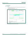
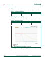
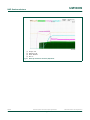
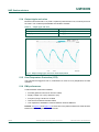
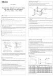
UM10899 TEA1833DB1361 45 W demo board Rev. 1 — 26 August 2015 User manual Document information Info Content Keywords TEA1833DB1361, TEA1833TS, TEA1833LTS, notebook adapter Abstract This user manual provides the specification, schematics and PCB layout of the TEA1833DB1361 45 W (90 W peak) demo board. See the data sheet and application note for more information on the TEA1833TS/LTS IC. UM10899 NXP Semiconductors TEA1833DB1361 45 W demo board Revision history Rev Date Description v.1 20150826 first issue Contact information For more information, please visit: http://www.nxp.com For sales office addresses, please send an email to: [email protected] UM10899 User manual All information provided in this document is subject to legal disclaimers. Rev. 1 — 26 August 2015 © NXP Semiconductors N.V. 2015. All rights reserved. 2 of 27 UM10899 NXP Semiconductors TEA1833DB1361 45 W demo board 1. Introduction WARNING Lethal voltage and fire ignition hazard The non-insulated high voltages that are present when operating this product, constitute a risk of electric shock, personal injury, death and/or ignition of fire. This product is intended for evaluation purposes only. It shall be operated in a designated test area by personnel qualified according to local requirements and labor laws to work with non-insulated mains voltages and high-voltage circuits. This product shall never be operated unattended. The TEA1833DB1361 demo board demonstrates the capabilities of the low-cost 6-pin TEA1833TS/LTS Switched-Mode Power Supply (SMPS) controller. This user manual describes the specification, the schematics, and the PCB layout of the TEA1833DB1361 45 W demo board. See the data sheet and application note for more information on the TEA1833TS/LTS IC. Remark: Unless otherwise specified, all values are typical values. 1.1 Features • • • • • • • • • • • • • • • UM10899 User manual Low no-load power (< 55 mW at 230 V (AC), output still in regulation) 200 % peak power Universal mains supply operation Low ripple and noise Small form factor Low-cost design Frequency reduction at low load to improve efficiency Efficiency DoE 2016 and COC 2014 compliant EMI CISPR22 compliant Brownin and brownout protection Output OverVoltage Protection (OVP) OverTemperature Protection (OTP) OverPower Protection with high/low compensation OverCurrent Protection (OCP) Output Short Circuit Protection (OSCP) All information provided in this document is subject to legal disclaimers. Rev. 1 — 26 August 2015 © NXP Semiconductors N.V. 2015. All rights reserved. 3 of 27 UM10899 NXP Semiconductors TEA1833DB1361 45 W demo board 2. Safety warning The TEA1833DB1361 demo board input is connected to the mains voltage. Avoid touching the board while it is connected to the mains voltage and when it is in operation. An isolated housing is obligatory when used in uncontrolled, non-laboratory environments. Galvanic isolation from the mains phase using a fixed or variable transformer is always recommended. Figure 1 shows the symbols on how to recognize these devices. 019aab174 019aab173 a. Isolated Fig 1. UM10899 User manual b. Not isolated Isolation symbols All information provided in this document is subject to legal disclaimers. Rev. 1 — 26 August 2015 © NXP Semiconductors N.V. 2015. All rights reserved. 4 of 27 UM10899 NXP Semiconductors TEA1833DB1361 45 W demo board 3. Power supply specification Table 1 lists the specification of the TEA1833DB1361 demo board. Table 1. TEA1833DB1361 specifications Symbol Parameter Value Vi input voltage 90 V to 264 V fi input frequency 47 Hz to 64 Hz Pi input power < 55 mW; no-load Vo output voltage 19.5 V Vo(ripple)(p-p) ripple output voltage < 150 mV (p-p); full load; 20 MHz bandwidth; 10 F capacitor at end of cable Po(nom) nominal output power 45 W Po(peak) peak output power > 90 W; 2 ms peak load during 50 % continuous load; 100 V (AC); 50 Hz; measured at end of cable Vo(peak) output voltage during peak load > 18 V; 2 ms 200 % peak load during 50 % continuous load; 100 V (AC); 50 Hz; measured at end of cable tholdup hold-up time > 5 ms; 115 V (AC); 60 Hz; full load tstartup start-up time < 2 s; 115 V (AC); 60 Hz < 3 s; 90 V (AC); 60 Hz efficiency > 89 %; average; measured at end of cable > 88 %; at 10 % load > 60 %; at 0.6 % load (= at 270 mW load) UM10899 User manual Vline(reg) line voltage regulation < 1 %; 90 V (AC) to 264 V (AC); measured at the PCB Vload(reg) load voltage regulation < 1 %; no-load to full load (2.3 A); measured at the PCB EMI conducted EMI > 5 dB margin; according to CISPR22 Po(opp) OPP trigger level 55 W to 65 W; over full input voltage range VO(ovp) overvoltage protection output voltage < 24 V (DC) Vbi brownin voltage 75 V (AC) to 85 V (AC) Vbo brownout voltage 65 V (AC) to 75 V (AC); over full load range Pi(shorted_output) average input power at continuously shorted output < 1 W; 264 V (AC) Totp overtemperature protection temperature 105 C; ±5 C; diode and NTC same temperature All information provided in this document is subject to legal disclaimers. Rev. 1 — 26 August 2015 © NXP Semiconductors N.V. 2015. All rights reserved. 5 of 27 UM10899 NXP Semiconductors TEA1833DB1361 45 W demo board 4. Board photographs Fig 2. UM10899 User manual TEA1833DB1361 demo board photograph - Top view All information provided in this document is subject to legal disclaimers. Rev. 1 — 26 August 2015 © NXP Semiconductors N.V. 2015. All rights reserved. 6 of 27 UM10899 NXP Semiconductors TEA1833DB1361 45 W demo board 5. Performance Performance figures are based on PCB design: • Schematic version: v.3 (see Figure 15) 5.1 Efficiency Efficiency measurements are taken using an automated test program containing a temperature stability detection algorithm. The output voltage and output current are measured using a 4-wire current sense configuration directly at the PCB connector. Measurements are performed for: • 115 V/60 Hz • 230 V/50 Hz Table 2. High load efficiency Measured directly at the PCB; see Section 5.1.1 for more information about how to calculate efficiency at end of cable. Condition Efficiency at specified load 10 %; 4.5 W 25 %; 11.25 W 50 %; 22.5 W 75 %; 33.75 W 100 %; 45 W 4-point average 115 V (AC)/60 Hz 89.21 % 90.61 % 90.36 % 90.01 % 89.21 % 90.05 % 230 V (AC)/50 Hz 88.41 % 90.61 % 90.57 % 90.70 % 90.64 % 90.63 % Table 3. Low load efficiency Measured directly at the PCB Condition Efficiency at specified load 0.2 W; 0.44 % 0.5 W; 1.11 % 1 W; 2.22 % 2 W; 4.44 % 115 V (AC)/60 Hz 78.44 % 86.00 % 88.30 % 89.48 % 230 V (AC)/50 Hz 70.21 % 81.31 % 84.93 % 86.91 % After subtracting 0.975 % from the 4-point average efficiency result for cable losses, the board complies with all efficiency standards listed below. Table 4. Efficiency standards Standard 10 % load 4-point average (25 %; 50 %; 75 %; 100 %) COC 2014 78.43 % 88.43 % COC 2016 78.85 % 88.85 % DoE 2008 - 84.26 % DoE 2016 - 87.73 % Energy Star 2.0 - 86.03 % 5.1.1 Cable loss At full load, the cable loss reduces the efficiency by: 2 2 I nom R cable 2.3 A R cable P cable = -------------------- 100 % = -------------------------------- 100 % = ---------------------------------------- 100 % P nom P nom 0.9 45 W (1) = R cable 13 % UM10899 User manual All information provided in this document is subject to legal disclaimers. Rev. 1 — 26 August 2015 © NXP Semiconductors N.V. 2015. All rights reserved. 7 of 27 UM10899 NXP Semiconductors TEA1833DB1361 45 W demo board • The resistance of a 1.8 m 20 AWG cable is approximately 120 m which reduces the efficiency at full load by 13 % 120 m = 1.56 % . • For the 4-point average, the result of the formula above must be multiplied by 0.6251 so for the 4-point average the efficiency is reduced by 0.97 %. • At a 10 % load, the influence of the cable can already be neglected. Table 5. Cable loss for different types of cable Cable thickness (AWG) Cable length (m) Resistance at 20 C (m) Efficiency loss (4-point average) (%) 16 1.2 32 0.26 1.8 47 0.39 1.2 50 0.41 1.8 75 0.71 1.2 80 0.65 1.8 120 0.97 18 20 5.1.2 Output diode Replacing the 20 A Schottky diode (D5 in Figure 15) by a 40 A Schottky diode, for example, the Vishay V40100C can improve the efficiency about 0.5 %. 5.2 No-load power consumption Measurement details: • • • • Power meter Yokogawa WT210 Integrated over 36 s AC source Agilent 6812B No probes or ground clips connected to board Table 6. Input condition No-load power 90 V (AC)/60 Hz 25.7 mW 115 V (AC)/60 Hz 28.5 mW 230 V (AC)/50 Hz 51.3 mW 264 V (AC)/50 Hz 62.0 mW Table 7. 1. No-load power measurements No-load power requirements Standard No-load power COC 2014 150 mW COC 2016 75 mW DoE 2008 300 mW DoE 2016 100 mW Energy Star 2.0 300 mW At low output current, the cable losses rapidly decrease: reducing the output current by a factor 2 decreases the cable losses by a factor 4. UM10899 User manual All information provided in this document is subject to legal disclaimers. Rev. 1 — 26 August 2015 © NXP Semiconductors N.V. 2015. All rights reserved. 8 of 27 UM10899 NXP Semiconductors TEA1833DB1361 45 W demo board 5.3 Load regulation The output voltage as a function of load current is measured directly at the PCB and at the end of the cable at 115 V (AC)/60 Hz. DDD 9R 9 ,2$ (1) Measured at the PCB. (2) Measured at the end of the cable. Fig 3. Output voltage as a function of output current 5.4 Line regulation The output voltage as a function of mains input voltage is measured directly at the PCB at full load (2.3 A) and at 60 Hz. DDD 9R 9 Fig 4. UM10899 User manual 9PDLQV9$& Output voltage as a function of mains voltage All information provided in this document is subject to legal disclaimers. Rev. 1 — 26 August 2015 © NXP Semiconductors N.V. 2015. All rights reserved. 9 of 27 UM10899 NXP Semiconductors TEA1833DB1361 45 W demo board 5.5 High/low line compensation The maximum continuous output power is measured at the PCB as function of the mains voltage at 60 Hz. DDD 3R : Fig 5. 9PDLQV$&9 Overpower protection threshold as a function of mains voltage If necessary, the OPP level can be increased by decreasing resistors R11 and R12 to 0.47 and increasing capacitor C1 to 82 F. In that case resistor R13 must be increased to limit the output power at high input voltages. See the TEA1833 application note (Ref. 3) for more information about how to tune R13 and R27. UM10899 User manual All information provided in this document is subject to legal disclaimers. Rev. 1 — 26 August 2015 © NXP Semiconductors N.V. 2015. All rights reserved. 10 of 27 UM10899 NXP Semiconductors TEA1833DB1361 45 W demo board 5.6 Peak power 5.6.1 Example 1 • Load: 200 % peak (4.6 A) for 2 ms when continuously running at 50 % load (10 ms) • Input voltage: 100 V (AC); 47 Hz • Output voltage: remains above 18 V (18.55 V) Green: Output current Blue: Output voltage (bottom of screen is 15 V) Fig 6. 200 % peak load for 2 ms when continuously running at 50 % load (accumulated over 30 s) The output voltage was measured at end of the cable. UM10899 User manual All information provided in this document is subject to legal disclaimers. Rev. 1 — 26 August 2015 © NXP Semiconductors N.V. 2015. All rights reserved. 11 of 27 UM10899 NXP Semiconductors TEA1833DB1361 45 W demo board 5.6.2 Example 2 • Load: 200 % peak (4.6 A) for 1 ms when continuously running at 100 % load (10 ms) • Input voltage: 90 V (AC); 47 Hz • Output voltage: remains above 17 V (17.66 V) Green: Output current Blue: Output voltage (bottom of screen is 15 V) Fig 7. 200 % peak load for 1 ms when continuously running at 100 % load (accumulated over 30 s) The output voltage was measured at end of the cable. For an even higher or longer peak load, decrease current sense resistor and increase bulk capacitor (also increases the maximum continuous output power) or increase the output capacitor. 5.7 VCC voltage The VCC voltage is measured at different input and loading conditions. It is within a safe margin of the UVLO level and the OVP level. Table 8. VCC voltage The two voltages are the minimum and the maximum value of the VCC ripple. UM10899 User manual Condition 90 V (AC)/60 Hz 264 V (AC)/50 Hz no-load 13.55 V to 18.05 V 13.85 V to 18.30 V 90 W peak load 27.10 V to 27.85 V 26.05 V to 26.75 V All information provided in this document is subject to legal disclaimers. Rev. 1 — 26 August 2015 © NXP Semiconductors N.V. 2015. All rights reserved. 12 of 27 UM10899 NXP Semiconductors TEA1833DB1361 45 W demo board 5.8 Brownout and start-up level Brownout and start-up level were measured at no-load and at full load in 0.5 V steps. Table 9. Brownout and start-up level Condition Start-up voltage Brownout voltage no-load 83.5 V (AC) 73.5 V (AC) full load (2.3 A) 83.5 V (AC) 75.0 V (AC) 5.9 OverVoltage Protection (OVP) Applying a short circuit across the LED of the photocoupler (U2) creates an output overvoltage condition. The output voltage is measured directly at the PCB. Table 10. Maximum output voltage Condition 115 V (AC)/60 Hz 230 V (AC)/50 Hz no-load 23.7 V 23.7 V full load (2.3 A) 23.7 V 23.7 V (1) Orange: VCC (2) Blue: Vo Fig 8. Overvoltage protection (230 V (AC)/50 Hz; full load) The OVP trigger level can be adjusted by changing resistor R27. For example, decreasing R27 to 68 k decreases the OVP trigger level to 21.8 V. UM10899 User manual All information provided in this document is subject to legal disclaimers. Rev. 1 — 26 August 2015 © NXP Semiconductors N.V. 2015. All rights reserved. 13 of 27 UM10899 NXP Semiconductors TEA1833DB1361 45 W demo board 5.10 Start-up time The start-up time was measured without connecting any voltage probes. All capacitors were fully discharged before starting up. Table 11. Start-up time measured at three input voltages Input voltage Start-up time 90 V (AC)/60 Hz 2.35 s 115 V (AC)/60 Hz 1.56 s 230 V (AC)/50 Hz 0.64 s 5.11 Start-up sequence Figure 9 and Figure 10 show waveforms of some essential voltages. These waveforms were captured during start-up at full load. (1) Orange: VCC (2) Magenta: CTRL (3) Green: DRIVER (4) Blue: Vo Fig 9. UM10899 User manual Start-up waveforms at 115 V (AC)/60 Hz All information provided in this document is subject to legal disclaimers. Rev. 1 — 26 August 2015 © NXP Semiconductors N.V. 2015. All rights reserved. 14 of 27 UM10899 NXP Semiconductors TEA1833DB1361 45 W demo board (1) Orange: VCC (2) Magenta: CTRL (3) Green: DRIVER (4) Blue: Vo Fig 10. Start-up waveforms at 230 V (AC)/50 Hz UM10899 User manual All information provided in this document is subject to legal disclaimers. Rev. 1 — 26 August 2015 © NXP Semiconductors N.V. 2015. All rights reserved. 15 of 27 UM10899 NXP Semiconductors TEA1833DB1361 45 W demo board 5.12 Hold-up time The hold-up time at 115 V (AC)/50 Hz is 9.5 ms. (1) Orange: VCC (2) Green: DRIVER (3) Magenta: CTRL (4) Blue: Bulk capacitor voltage Fig 11. Hold-up time at 115 V (AC)/50 Hz The hold-up time was measured from the last valley of the bulk capacitor ripple (worst case moment for mains interruption) until the output voltage starts to drop (drops to below 18.5 V). 5.13 Average input power at continuously shorted output Measurement details: • • • • Output was shorted at the end of the cable Power meter Yokogawa WT210 Current range 5 A Integration time 36 s Table 12. UM10899 User manual Input power at continuously shorted output Condition Input power 90 V (AC)/60 Hz 167 mW 115 V (AC)/60 Hz 179 mW 230 V (AC)/50 Hz 596 mW 264 V (AC)/50 Hz 721 mW All information provided in this document is subject to legal disclaimers. Rev. 1 — 26 August 2015 © NXP Semiconductors N.V. 2015. All rights reserved. 16 of 27 UM10899 NXP Semiconductors TEA1833DB1361 45 W demo board 5.14 Output ripple and noise Measured at full load with a 10 F/50 V capacitor (United Chemi Con; KY series) at end of the cable. The oscilloscope bandwidth was limited to 20 MHz. Table 13. Output ripple and noise Condition Vo(ripple)(p-p) 90 V (AC) 81 mV (p-p) 264 V (AC) 81 mV (p-p) Fig 12. Output voltage ripple and noise at 264 V (AC)/50 Hz 5.15 OverTemperature Protection (OTP) The external OTP triggers at 105 C, measured in an oven at 115 V (AC)/60 Hz at no-load operation. 5.16 EMI performance Conducted EMI measurement details: • • • • • Full load (passive load 8.33 at end of cable) Supply voltage 115 V (AC) and 230 V (AC) Frequency range 150 kHz to 30 MHz Test receiver Rohde & Schwarz ESPI3 Line impedance stabilization network Rohde & Schwarz ENV216 Remark: In Figure 13 and Figure 14, the blue line is the peak measurement result and the black line is the average measurement result. UM10899 User manual All information provided in this document is subject to legal disclaimers. Rev. 1 — 26 August 2015 © NXP Semiconductors N.V. 2015. All rights reserved. 17 of 27 UM10899 NXP Semiconductors TEA1833DB1361 45 W demo board a. Line b. Neutral Fig 13. Conducted EMI performance at 115 V (AC)/60 Hz a. Line b. Neutral Fig 14. Conducted EMI performance at 230 V (AC)/50 Hz UM10899 User manual All information provided in this document is subject to legal disclaimers. Rev. 1 — 26 August 2015 © NXP Semiconductors N.V. 2015. All rights reserved. 18 of 27 UM10899 NXP Semiconductors TEA1833DB1361 45 W demo board 6. Schematic ; PDLQVLQOHW 5 ȍ ) $ 9 %' .30* / ' 1;36+&; 5 ȍ %'G %'E &; Q) 9 %'D & ) 9 %'F :% ZLUHEULGJH & Q) 9 :% ' 5 0ȍ 5 0ȍ 5 0ȍ 5 0ȍ %$9: 'D ' ' %$6+ 8 *1' 3527(&7 7($76 7623 '5,9(5 ' %$6 5 ȍ 5 ,6(16( &75/ 7 50 /S+ W /) RSWLRQDO ; 287387 &$%/( *1' 5 Nȍ 8 92/$;7 & Q) & Q) RSWLRQDO & S)N9 KHDWVLQN IRU4 5 ȍ & Q) 9 $ ZLUHEULGJH Nȍ 8 92/$;7 & Q) 4 7.$ 5 ȍ & Q) ' %$6 RSWLRQDO 5 ȍ & ) 9 )O\BWRS W )O\BERWWRP RSWLRQDO & S)9 ' %$6+ / + 5 Nȍ W $ & Q) W 9 ' 6$0 & ) 9 9&& 5 Nȍ [%=;& 'E 5 0ȍ & Q) 9 KHDWVLQN IRU' /) 1 5 0ȍ & S) 5 Nȍ 5 Nȍ 5 0ȍ 8 1&3$& 5 Nȍ 5 ȍ &< Q) 5 ȍ 57 Nȍ#& Nȍ#& DDD Fig 15. TEA1833DB1361 schematic UM10899 User manual All information provided in this document is subject to legal disclaimers. Rev. 1 — 26 August 2015 © NXP Semiconductors N.V. 2015. All rights reserved. 19 of 27 UM10899 NXP Semiconductors TEA1833DB1361 45 W demo board 7. Bill Of Materials (BOM) Table 14. TEA1833DB1361 bill of materials Reference Description and values Part number Manufacturer BC1 not mounted; ferrite core; on pin CY1 74270073 Würth Elektronik BD1 bridge diode; 2 A; 600 V KBP206G Diodes Inc. C1 capacitor; 68 F; 400 V; 105 C 400BXW68MEFC18X20 Rubycon C2 capacitor; 3.3 nF; 1 kV; X7R; 1206 - - C3 capacitor; 2.2 nF; 630 V; X7R; 1206 - - C4 capacitor; not mounted; 100 pF; 1 kV; X7R; 1206 - - C7 capacitor; 100 nF; 50 V; X7R; 0603 - - C9; C10; C15 capacitor; 1 nF; 50 V; X7R; 0603 - - C11 capacitor; 2.2 F; 50 V; 105 C; 5 mm 11 mm 50YXJ2R2MTA5X11 Rubycon C13 capacitor; 680 F; 25 V; 105 C; 10 mm 20 mm EKZE250ELL681MJ20S United Chemi Con C16 capacitor; 10 nF; 50 V; X7R; 0603 - - C18 capacitor; 220 pF; 100 V; NPO; 0805 - - C19 capacitor; 100 nF; 50 V; X7R; 1206 - - C20 capacitor; not mounted; 220 pF; 50 V; X7R; 0603 - - CX1 capacitor; 220 nF; 275 V (AC); X2 - HJC CY1 capacitor; 1.5 nF; 250 V (AC); Y1 DE1E3KX152MA5BA01 Murata D1 diode; 1 kV; 2 A SA2M-E3/61T Vishay D2 diode; 100 V; 250 mA BAS316 NXP Semiconductors D3; D8 diode; 200 V; 200 mA BAS21H NXP Semiconductors D5 diode; Schottky; 100 V; 2 10 A; TO220 NXPS20H100CX NXP Semiconductors D6 diode; 85 V; 200 mA BAS416 NXP Semiconductors D7 diode; dual; common cathode; 85 V; 100 mA BAV70W NXP Semiconductors D9; D10 diode; Zener; 75 V; 250 mW; SOD323F BZX84J-B75 NXP Semiconductors F1 fuse; slow blow; 3.15 A; 250 V (AC) MST 3.15A 250V Multicomp HS1 heat sink for Q1 - - HS2 heat sink for D5 - - L1 inductor; 3.3 H; 1.2 A LQM2HPN3R3MG0L Murata LF1 choke; common mode; not mounted; shorted by wire bridge; diameter = 0.8 mm; pitch 5.08 mm - - LF2 choke; common mode; 2 6.8 mH B82721K2122N20 EPCOS M1; M2 screw; M3 8; for mounting Q1 and D5 - - M3; M4 spring washer; M3; for mounting Q1 and D5 - - M5; M6 nut; M3; for mounting Q1 and D5 - - Q1 MOSFET; N-channel; 600 V; 10 A TK10A60D Toshiba UM10899 User manual All information provided in this document is subject to legal disclaimers. Rev. 1 — 26 August 2015 © NXP Semiconductors N.V. 2015. All rights reserved. 20 of 27 UM10899 NXP Semiconductors TEA1833DB1361 45 W demo board Table 14. TEA1833DB1361 bill of materials …continued Reference Description and values Part number Manufacturer R1; R2; R3; R8 resistor; 1.2 M; 1206 - - R5; R6 resistor; 10 M; 1 %; 1206 - - R11; R12 resistor; 0.51 ; 1 %; 500 mW; 1206 - - R13 resistor; 9.1 k; 1 %; 0603 - - R14 resistor; 150 ; 0805 - - R15 resistor; 4.7 ; 0805 - - R17 resistor; 2.7 k; 1 %; 0603 - - R20 resistor; 1.0 k; 0805 - - R22 resistor; 10 k; 0603 - - R23 resistor; 180 k; 1 %; 0603 - - R24 resistor; 24 k; 1 %; 0603 - - R25 resistor; 2.2 M; 0603 - - R26 resistor; 47 ; 0805 - - R27 resistor; 75 k; 1 %; 0603 - - R28 resistor; 0 ; 2512 - - R29 resistor; 0 ; 0603 - - R30 resistor; not mounted; 47 ; 0603 - - RT1 resistor; NTC; 100 k NTCLE100E3104JB0 Vishay T1 transformer; RM8 (see Section 9) TF-RM080-207R Shenzhen Belta U1 flyback controller TEA1833TS NXP Semiconductors U2 photocoupler; CTR = 100 % to 200 % at IF = 1 mA VOL618A-3X001T Vishay U3 shunt regulator; 2.5 V NCP431ACSNT1G ON Semiconductor WB1; WB2 wire bridge; diameter = 0.8 mm; pitch = 5.08 mm - - X1 mains inlet 770W-X2/10 Qualtek X2 output cable; 20 AWG; 1.8 m - - UM10899 User manual All information provided in this document is subject to legal disclaimers. Rev. 1 — 26 August 2015 © NXP Semiconductors N.V. 2015. All rights reserved. 21 of 27 UM10899 NXP Semiconductors TEA1833DB1361 45 W demo board 8. PCB layout Fig 16. Copper layout bottom side (top view) a. Top b. Bottom Fig 17. Component placing (top view) UM10899 User manual All information provided in this document is subject to legal disclaimers. Rev. 1 — 26 August 2015 © NXP Semiconductors N.V. 2015. All rights reserved. 22 of 27 UM10899 NXP Semiconductors TEA1833DB1361 45 W demo board 9. Transformer specification • Manufacturer: Shenzhen Belta Technology Co. Ltd. • Shenzhen Belta part number: TF-RM080-207R PP PD[ PP PD[ EXON )O\BWRS9RXW 1 SULPDU\ ZLQGLQJ W W $ 1 1 VHFRQGDU\ ZLQGLQJ W )O\BERWWRPVHFJQG GUDLQ 9DX[ DX[LOLDU\ ZLQGLQJ 1 PP PP W SULPJQG SULPJQG PP VKLHOG ZLQGLQJ 1 PP W QF SULPJQG FRUHFRQQHFWLRQWR SLQSULPJQG KROHDUUDQJHPHQW YLHZLQPRXQWLQJGLUHFWLRQ DDD Fig 18. Transformer specification UM10899 User manual All information provided in this document is subject to legal disclaimers. Rev. 1 — 26 August 2015 © NXP Semiconductors N.V. 2015. All rights reserved. 23 of 27 UM10899 NXP Semiconductors TEA1833DB1361 45 W demo board Table 15. Electrical characteristics Parameter Value Conditions DC resistance 1110 m primary 45 m secondary 527 m auxiliary 650 H 10 kHz 5.8 H 100 kHz; 100 mV (RMS) prim:sec:auxiliary 5.67:1.0:1.0 primary inductance leakage inductance[1] winding ratio [1] Secondary and auxiliary winding shorted Table 16. UM10899 User manual Winding specification Winding[1] Wire N1 1 0.224 mm N2 4 0.18 mm 10 pin 10 - shield N3 1 0.5 mm TEX-E 12 fly top fly bottom secondary N4 1 0.224 mm 34 A[2] pin 1 primary N5 1 0.15 mm 12 pin 10 pin 11 auxiliary Turns 34 Start Finish Purpose pin 3 A[2] primary [1] 1 layer of mylar tape after each winding. [2] Intermediate connection A is not connected to a pin. All information provided in this document is subject to legal disclaimers. Rev. 1 — 26 August 2015 © NXP Semiconductors N.V. 2015. All rights reserved. 24 of 27 UM10899 NXP Semiconductors TEA1833DB1361 45 W demo board 10. Abbreviations Table 17. Abbreviations Acronym Description SMPS Switched-Mode Power Supply OCP OverCurrent Protection OPP OverPower Protection OTP OverTemperature Protection UVLO UnderVoltage LockOut LED Light-Emitting Diode OVP OverVoltage Protection EMI ElectroMagnetic Interference 11. References UM10899 User manual [1] TEA1833TS data sheet — GreenChip SMPS control IC [2] TEA1833LTS data sheet — GreenChip SMPS control IC [3] AN11675 application note — GreenChip TEA1833(L)TS fixed frequency flyback controller All information provided in this document is subject to legal disclaimers. Rev. 1 — 26 August 2015 © NXP Semiconductors N.V. 2015. All rights reserved. 25 of 27 UM10899 NXP Semiconductors TEA1833DB1361 45 W demo board 12. Legal information 12.1 Definitions Draft — The document is a draft version only. The content is still under internal review and subject to formal approval, which may result in modifications or additions. NXP Semiconductors does not give any representations or warranties as to the accuracy or completeness of information included herein and shall have no liability for the consequences of use of such information. NXP Semiconductors does not accept any liability related to any default, damage, costs or problem which is based on any weakness or default in the customer’s applications or products, or the application or use by customer’s third party customer(s). Customer is responsible for doing all necessary testing for the customer’s applications and products using NXP Semiconductors products in order to avoid a default of the applications and the products or of the application or use by customer’s third party customer(s). NXP does not accept any liability in this respect. Export control — This document as well as the item(s) described herein may be subject to export control regulations. Export might require a prior authorization from competent authorities. 12.2 Disclaimers Limited warranty and liability — Information in this document is believed to be accurate and reliable. However, NXP Semiconductors does not give any representations or warranties, expressed or implied, as to the accuracy or completeness of such information and shall have no liability for the consequences of use of such information. NXP Semiconductors takes no responsibility for the content in this document if provided by an information source outside of NXP Semiconductors. In no event shall NXP Semiconductors be liable for any indirect, incidental, punitive, special or consequential damages (including - without limitation - lost profits, lost savings, business interruption, costs related to the removal or replacement of any products or rework charges) whether or not such damages are based on tort (including negligence), warranty, breach of contract or any other legal theory. Notwithstanding any damages that customer might incur for any reason whatsoever, NXP Semiconductors’ aggregate and cumulative liability towards customer for the products described herein shall be limited in accordance with the Terms and conditions of commercial sale of NXP Semiconductors. Right to make changes — NXP Semiconductors reserves the right to make changes to information published in this document, including without limitation specifications and product descriptions, at any time and without notice. This document supersedes and replaces all information supplied prior to the publication hereof. Suitability for use — NXP Semiconductors products are not designed, authorized or warranted to be suitable for use in life support, life-critical or safety-critical systems or equipment, nor in applications where failure or malfunction of an NXP Semiconductors product can reasonably be expected to result in personal injury, death or severe property or environmental damage. NXP Semiconductors and its suppliers accept no liability for inclusion and/or use of NXP Semiconductors products in such equipment or applications and therefore such inclusion and/or use is at the customer’s own risk. Applications — Applications that are described herein for any of these products are for illustrative purposes only. NXP Semiconductors makes no representation or warranty that such applications will be suitable for the specified use without further testing or modification. Customers are responsible for the design and operation of their applications and products using NXP Semiconductors products, and NXP Semiconductors accepts no liability for any assistance with applications or customer product design. It is customer’s sole responsibility to determine whether the NXP Semiconductors product is suitable and fit for the customer’s applications and products planned, as well as for the planned application and use of customer’s third party customer(s). Customers should provide appropriate design and operating safeguards to minimize the risks associated with their applications and products. Evaluation products — This product is provided on an “as is” and “with all faults” basis for evaluation purposes only. NXP Semiconductors, its affiliates and their suppliers expressly disclaim all warranties, whether express, implied or statutory, including but not limited to the implied warranties of non-infringement, merchantability and fitness for a particular purpose. The entire risk as to the quality, or arising out of the use or performance, of this product remains with customer. In no event shall NXP Semiconductors, its affiliates or their suppliers be liable to customer for any special, indirect, consequential, punitive or incidental damages (including without limitation damages for loss of business, business interruption, loss of use, loss of data or information, and the like) arising out the use of or inability to use the product, whether or not based on tort (including negligence), strict liability, breach of contract, breach of warranty or any other theory, even if advised of the possibility of such damages. Notwithstanding any damages that customer might incur for any reason whatsoever (including without limitation, all damages referenced above and all direct or general damages), the entire liability of NXP Semiconductors, its affiliates and their suppliers and customer’s exclusive remedy for all of the foregoing shall be limited to actual damages incurred by customer based on reasonable reliance up to the greater of the amount actually paid by customer for the product or five dollars (US$5.00). The foregoing limitations, exclusions and disclaimers shall apply to the maximum extent permitted by applicable law, even if any remedy fails of its essential purpose. Safety of high-voltage evaluation products — The non-insulated high voltages that are present when operating this product, constitute a risk of electric shock, personal injury, death and/or ignition of fire. This product is intended for evaluation purposes only. It shall be operated in a designated test area by personnel that is qualified according to local requirements and labor laws to work with non-insulated mains voltages and high-voltage circuits. The product does not comply with IEC 60950 based national or regional safety standards. NXP Semiconductors does not accept any liability for damages incurred due to inappropriate use of this product or related to non-insulated high voltages. Any use of this product is at customer’s own risk and liability. The customer shall fully indemnify and hold harmless NXP Semiconductors from any liability, damages and claims resulting from the use of the product. Translations — A non-English (translated) version of a document is for reference only. The English version shall prevail in case of any discrepancy between the translated and English versions. 12.3 Trademarks Notice: All referenced brands, product names, service names and trademarks are the property of their respective owners. GreenChip — is a trademark of NXP Semiconductors N.V. UM10899 User manual All information provided in this document is subject to legal disclaimers. Rev. 1 — 26 August 2015 © NXP Semiconductors N.V. 2015. All rights reserved. 26 of 27 UM10899 NXP Semiconductors TEA1833DB1361 45 W demo board 13. Contents 1 1.1 2 3 4 5 5.1 5.1.1 5.1.2 5.2 5.3 5.4 5.5 5.6 5.6.1 5.6.2 5.7 5.8 5.9 5.10 5.11 5.12 5.13 5.14 5.15 5.16 6 7 8 9 10 11 12 12.1 12.2 12.3 13 Introduction . . . . . . . . . . . . . . . . . . . . . . . . . . . . 3 Features . . . . . . . . . . . . . . . . . . . . . . . . . . . . . . 3 Safety warning . . . . . . . . . . . . . . . . . . . . . . . . . . 4 Power supply specification. . . . . . . . . . . . . . . . 5 Board photographs . . . . . . . . . . . . . . . . . . . . . . 6 Performance . . . . . . . . . . . . . . . . . . . . . . . . . . . . 7 Efficiency . . . . . . . . . . . . . . . . . . . . . . . . . . . . . 7 Cable loss . . . . . . . . . . . . . . . . . . . . . . . . . . . . . 7 Output diode . . . . . . . . . . . . . . . . . . . . . . . . . . . 8 No-load power consumption . . . . . . . . . . . . . . . 8 Load regulation . . . . . . . . . . . . . . . . . . . . . . . . . 9 Line regulation . . . . . . . . . . . . . . . . . . . . . . . . . 9 High/low line compensation . . . . . . . . . . . . . . 10 Peak power. . . . . . . . . . . . . . . . . . . . . . . . . . . 11 Example 1. . . . . . . . . . . . . . . . . . . . . . . . . . . . 11 Example 2. . . . . . . . . . . . . . . . . . . . . . . . . . . . 12 VCC voltage . . . . . . . . . . . . . . . . . . . . . . . . . . 12 Brownout and start-up level . . . . . . . . . . . . . . 13 OverVoltage Protection (OVP) . . . . . . . . . . . . 13 Start-up time . . . . . . . . . . . . . . . . . . . . . . . . . . 14 Start-up sequence. . . . . . . . . . . . . . . . . . . . . . 14 Hold-up time . . . . . . . . . . . . . . . . . . . . . . . . . . 16 Average input power at continuously shorted output . . . . . . . . . . . . . . . . . . . . . . . . . . . . . . . 16 Output ripple and noise . . . . . . . . . . . . . . . . . 17 OverTemperature Protection (OTP) . . . . . . . . 17 EMI performance . . . . . . . . . . . . . . . . . . . . . . 17 Schematic . . . . . . . . . . . . . . . . . . . . . . . . . . . . . 19 Bill Of Materials (BOM) . . . . . . . . . . . . . . . . . . 20 PCB layout . . . . . . . . . . . . . . . . . . . . . . . . . . . . 22 Transformer specification . . . . . . . . . . . . . . . . 23 Abbreviations . . . . . . . . . . . . . . . . . . . . . . . . . . 25 References . . . . . . . . . . . . . . . . . . . . . . . . . . . . 25 Legal information. . . . . . . . . . . . . . . . . . . . . . . 26 Definitions . . . . . . . . . . . . . . . . . . . . . . . . . . . . 26 Disclaimers . . . . . . . . . . . . . . . . . . . . . . . . . . . 26 Trademarks. . . . . . . . . . . . . . . . . . . . . . . . . . . 26 Contents . . . . . . . . . . . . . . . . . . . . . . . . . . . . . . 27 Please be aware that important notices concerning this document and the product(s) described herein, have been included in section ‘Legal information’. © NXP Semiconductors N.V. 2015. All rights reserved. For more information, please visit: http://www.nxp.com For sales office addresses, please send an email to: [email protected] Date of release: 26 August 2015 Document identifier: UM10899