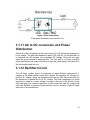
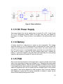
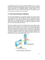
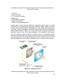
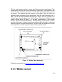
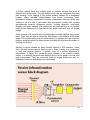
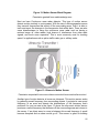
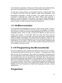
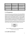
1
The A.U.M. Device
(pronounced “Ohm”)
By
B. Löwen Gruseck
Gardy Lacombe
Michael Sriprashad
1
Table of Contents
1. Executive Summary ...................................................................................................... 1
2. Project Description ........................................................................................................ 2
2.1 Project Motivation .................................................................................................... 2
2.2 Goals and Objectives .............................................................................................. 3
2.2.1 Cost Efficiency .................................................................................................. 4
2.2.2 Energy Saving................................................................................................... 4
2.2.3 Touch Screen Interface..................................................................................... 4
2.2.4 Android Interface............................................................................................... 5
2.2.5 Motion Sensor ................................................................................................... 5
2.3 Scope of work.......................................................................................................... 5
2.3.1 Objectives ......................................................................................................... 6
2.3.2 Schedule ........................................................................................................... 6
2.3.3 Tasks ................................................................................................................ 6
2.4 Significance ............................................................................................................. 7
2.5 Specifications .......................................................................................................... 7
2.5.1 Main Features ................................................................................................... 7
2.5.2 AC To DC Conversion ...................................................................................... 8
2.5.3 Current Sensor Circuit ...................................................................................... 8
2.5.4 Power Relay...................................................................................................... 8
2.5.5 Automatic Utility and Device Control................................................................. 9
2.5.6 Wireless Control................................................................................................ 9
2.5.7 LCD Specification ............................................................................................. 9
2.5.8 Motion Sensor Specifications.......................................................................... 10
3. Research ..................................................................................................................... 11
3.1 Methods................................................................................................................. 11
3.1.1 Project Management ....................................................................................... 11
3.1.3 Current Sensor................................................................................................ 13
3.1.4 Shunt Resistor ................................................................................................ 13
3.1.5 Current Transformer ....................................................................................... 14
3.1.6 Hall Effect Current Sensor Transducer ........................................................... 15
3.1.7 Current Sensor................................................................................................ 17
3.1.8 Relay System .................................................................................................. 18
3.1.9 Electromechanical Relay ................................................................................ 18
3.1.10 Solid State Relay .......................................................................................... 18
i
3.1.11 AC to DC conversion and Power Distribution ............................................... 19
3.1.12 Rectifier Circuit.............................................................................................. 19
3.1.13 DC Power Supply.......................................................................................... 20
3.1.14 Battery........................................................................................................... 20
3.1.15 PCB............................................................................................................... 20
3.1.16 Touch Screen interface .................................................................................... 21
3.1.17 Motion sensor ............................................................................................... 23
3.1.18 Microcontroller .............................................................................................. 26
3.1.19 Programming the Microcontroller .................................................................. 26
3.1.20 Software ........................................................................................................ 27
3.1.21 Wireless Control............................................................................................ 29
3.2 Components .......................................................................................................... 30
3.2.1 ACS712........................................................................................................... 30
3.2.2 CSLT6B100 .................................................................................................... 31
3.2.3 Relay System Chosen .................................................................................... 32
3.2.4 LCD Screens................................................................................................... 33
3.2.5 Motion Sensor ................................................................................................. 34
3.2.6 Microcontroller ................................................................................................ 35
3.2.7 Programmer .................................................................................................... 37
3.2.8 Software .......................................................................................................... 39
3.2.9 Wireless Control.............................................................................................. 40
3.2.10 Wireless App Programming Software ........................................................... 43
3.2.11 Relevant Technologies ................................................................................. 45
4. Designs ....................................................................................................................... 48
4.1 Hardware ............................................................................................................... 48
4.1.1 Microcontroller ................................................................................................ 48
4.1.2 Programmer .................................................................................................... 50
4.1.3 LCD Touch Screen ......................................................................................... 50
4.1.4 Motion sensor ................................................................................................. 52
4.1.5 Power Supply .................................................................................................. 53
4.1.6 Current Sensor................................................................................................ 54
4.1.7 Solid State Relay ............................................................................................ 54
4.2 Circuit Design ........................................................................................................ 54
4.2.1 Solid State Relay Circuit ................................................................................. 54
4.2.2 Overall Device................................................................................................. 55
ii
4.2.3 Microcontroller Pin Configuration .................................................................... 56
4.2.4 Schematics ..................................................................................................... 58
4.3 Software ............................................................................................................. 59
4.3.1 Touch screen programming ............................................................................ 59
4.3.4 Value Calculations .......................................................................................... 71
4.3.5 Wireless Control.............................................................................................. 71
5. Prototype ..................................................................................................................... 73
6. Testing ........................................................................................................................ 76
6.1 Hardware ............................................................................................................... 76
6.1.1 Power Supply .................................................................................................. 76
6.1.2 Current Sensor circuit ..................................................................................... 76
6.1.3 Solid State Relay ............................................................................................ 76
6.1.4 Entire A.U.M. Device....................................................................................... 77
6.1.5 LCD ................................................................................................................. 78
6.1.6 Motion Sensor ................................................................................................. 78
6.2 Software Testing ................................................................................................... 78
6.2.1 Menu Testing...................................................................................................... 79
6.2.2 Home Screen .................................................................................................. 79
6.2.3 Leader/Follower mode .................................................................................... 79
6.2.4 Motion sense mode......................................................................................... 79
6.2.5 Standby mode ................................................................................................. 80
6.2.5 ON/OFF mode ................................................................................................ 80
6.2.6 Timed mode .................................................................................................... 81
6.2.7 Power mode .................................................................................................... 81
6.2.8 Estimated cost and power used ...................................................................... 81
6.2.9 Microcontroller Testing.................................................................................... 81
6.2.10 Microcontroller Accuracy............................................................................... 82
7. User Manual ................................................................................................................ 84
8. Administrative Content ................................................................................................ 90
8.1 Budget projection and financing ............................................................................ 90
8.2 Milestones ............................................................................................................. 91
8.3 Conclusion ................................................................................................................ 92
iii
Figures and Table
Figure 1: Power ratings ..................................................................................................... 3
Figure 2: Project Management Block Diagram ............................................................... 11
Figure 3: Complex Power ................................................................................................ 12
Figure 4: Shunt Resistor ................................................................................................. 14
Figure 5: Open loop Hall Effect ....................................................................................... 16
Figure 6: Closed Loop Hall Effect ................................................................................... 17
Figure 7:Solid State Relay .............................................................................................. 19
Figure 8: Made in Multisim .............................................................................................. 20
Figure 9: Resistive Touch Screen ................................................................................... 21
Figure 10: Capacitive Screen .......................................................................................... 22
Figure 11: Surface Wave Acoustics ................................................................................ 23
Figure 12: Motion Sensor Block Diagram ....................................................................... 25
Figure 13: Ultrasonic Motion Sensor ............................................................................... 25
Figure 14: Closed Loop Current Sensor ......................................................................... 31
Figure 15: MSP430 pin layout ......................................................................................... 36
Figure 16: BlueSMiRF RP-SMA pin layout ..................................................................... 42
Figure 17: Bluetooth Mate Gold pin layout ..................................................................... 43
Figure 18: LCG3 10-outlets power strip .......................................................................... 46
Figure 19: AVRISPmkII Serial connection cable header pin layout ................................ 50
Figure 20: LCD Touch Screen ........................................................................................ 51
Figure 21: PIR motion sensor ......................................................................................... 52
Figure 22: Flyback Converter .......................................................................................... 53
Figure 23: Solid State relay control ................................................................................. 55
Figure 24: Overall Device Block Diagram ....................................................................... 56
Figure 25: Pin Layout for the Atmega324p ..................................................................... 57
Figure 26: Overall Schematic Circuit ................................. Error! Bookmark not defined.
Figure 27: Printed Circuit Board ...................................................................................... 59
Figure 28: Final Printed Circuit Board ............................................................................. 59
Figure 29: Home Screen Block Diagram ......................................................................... 60
Figure 30: Leader Follower Block Diagram ..................................................................... 61
Figure 31: Motion sensing Block Diagram ...................................................................... 62
Figure 32: ON/OFF mode ............................................................................................... 63
Figure 33: Stand-by mode ............................................................................................... 64
Figure 34: Timer Mode Block Diagram ........................................................................... 65
Figure 35: Power mode block diagram ........................................................................... 66
Figure 36: Estimated cost and power used ..................................................................... 67
Figure 37: Algorithm Flowchart for automatic outlet control ............................................ 69
Figure 38: Prototype of the A.U.M. Device ...................................................................... 73
Figure 39: Home Menu ................................................................................................... 74
Figure 40: Outlet 1 .......................................................................................................... 74
Figure 41: Peripherals ..................................................................................................... 75
iv
Figure 42: A.U.M Device menu screen ........................................................................... 84
Figure 43: Standby Menu Screen ................................................................................... 85
Figure 44: Leader-Follower Screen ................................................................................. 85
Figure 45: Motion Sensing Screen .................................................................................. 86
Figure 46: On/Off Screen ................................................................................................ 86
Figure 47: Energy Saved Screen .................................................................................... 87
Figure 48: Timed Mode Screen ....................................................................................... 87
Figure 49: Power Screen ................................................................................................ 88
Figure 50: Wireless App Screen ..................................................................................... 89
v
1. Executive Summary
Vampire draw, Phantom load, or most commonly know as Standby power
accommodates about 10% of the total amount of wasted electricity in the world
and in your electricity bill. Devices such as the VCRs, all-in-one printers, and
laptops are all examples of the largest culprits. Using 50% of the power as if the
device was on while in standby mode. Even though in some cases being
necessary such as remote controls, observing temperatures, and digital displays,
these devices add up in the modern home and can also add a hefty tax to your
electricity bill. The solution to this would be to regulate which devices are left in
stand by mode and which devices should be completely unplugged or power cut.
Saving energy is important with the depletion of fuels. Alternative sources must
be created to be able to sustain our lifestyle and by saving energy this allows us
more time to be able to fabricate these sources.
We have created a device that is low power, user friendly and reduces the
amount of power wasted in stand by mode. By cutting all power to a device when
not in use this will eliminate standby power. The A.U.M. Device (pronounced
“Ohm”) or also known as the automated utility management device is similar to a
power strip but carries an LCD touch screen display for user interaction. This
device allows the user to regulate devices plugged in to be set on, completely off
or depending on surrounding devices. For example say we have the Computer,
monitor, and printer plugged in to the A.U.M. Device. The device can be set that
when the computer enters sleep or standby mode all power will be cut from the
surrounding devices therefore eliminating standby power.
This device also carries Bluetooth technology, which allows a user to link their
android device via Bluetooth to the A.U.M. Device. This will allow the user to
control the device up the 50 feet away. Being able to turn devices on and off from
anywhere in your home making the device easily accessible to the user that is
out of reach of the A.U.M. Device. It also carries an infrared motion sensor
located on the front of the A.U.M. Device that will be used to detect primarily if a
user has entered or exited the room. This allows for the A.U.M. Device to power
down all devices once a user has been gone for a period of time. The A.U.M.
Device also displays the in the menu of the LCD an average monthly power cost
for the devices connected to A.U.M. Device and your average electricity bill.
With Similar devices to the A.U.M. Device available we noticed that they did not
behold many features at all. They were mainly basic power strips with switches to
kill power to one of the outlet. The A.U.M. Device is designed to go above and
beyond these designs to create a product with useful features easily accessible
and user friendly to people of all ages. With wireless capabilities, infrared motion
fail-safe, and monthly power consumption to ensure that the most power is saved
even from rooms away.
1
2. Project Description
2.1 Project Motivation
Most people believe when they turn their device off, it’s not wasting any power.
That simply isn’t true because even when a device isn’t being used or in the ‘off’
mode, it’s still draining energy from the outlet. The United States department of
energy has defined standby power or phantom load as “The power consumed by
a product when in the lowest power consuming mode, which typically occurs
when the product is switched to “off” or not preforming it primary function or
purpose. An extreme number of electronics on the market today cannot be
completely turned off unless being unplugged from the outlet.
According to Forbes “A typical United States home has forty products constantly
drawing power, together these amount to almost 10% for residential electricity
use”. On average Standby power consumes about five percent to around fifteen
percent of electricity used in a modern residential home. This can add up to over
five hundred million dollars a year globally. Standby power is turning into a
growing epidemic for most households across the globe with the depletion of
fuels to produce electricity. Corresponding to the Lawrence Berkley national
laboratory (standy.lbl.gov), standby power contributes to one about percent of
global carbon dioxide emissions in our earth’s atmosphere, which is about 5
million tons of carbon dioxide per year. This is equivalent to impact on the
atmosphere of more than 1 million cars.
For some equipment such as fire alarms, security systems or thermostats require
the use of stand by power to stay powered throughout the day for daily and
emergency purposes. In turn we need to regulate which device should remain in
stand by mode and which should be completely turned off. As seen in figure 1.1
on the next page having theses device plugged in when not in use or idle will
cost you a considerable amount of money in the long run. Averaging up about
five hundred dollars just for the devices listed below in figure 1 table.
With the constant rise of cost of electricity we need to be more aware of where
our power is going and preserve as much of it as we can for future use. Our
group sought out to manufacture a device that eliminates standby power with
convenience. With a number of features for accessibility and an energy sufficient
design that will not only help with energy sustainability, it will also become
beneficiary to the entire planet. Along with saving money and retaining our
depleting fuel supply.
2
Figure 1: Power ratings
Permission granted from choice.au
2.2 Goals and Objectives
The main goal of our overall project was to create a device that improves energy
efficiency, demonstrate energy sustainability and can be completely monitored by
the user. We also aspire for the user to have minimal day-to-day interactions with
the device. With people always on the go we aimed at having at type of “worry
3
free” device. This design entails a total of three outlets. The A.U.M. Device is
comparable to a power strip in design but with an LCD touch screen. The A.U.M.
Device also informs you how much energy your appliances are drawing as well
as calculate your monthly electric bill.
2.2.1 Cost Efficiency
A major goal of ours was to fabricate a design that was low cost and effective.
This played a huge part in the project when choosing parts and design
methodology. We examined our situation and tried to find ways of breaking the
cost down little by little. For example with the microcontroller we researched over
twenty different kinds and compared specs to be able to choose a microcontroller
that was low power, low cost, and able to support all the features that are
currently available on our device. We also found ways to cut cost by buying in
bulk, and shopping around for parts through different vendors
2.2.2 Energy Saving
Considerably the most important goal of our project was to conserve the use of
energy of devices while a device is in stand by mode. Our device carries three
outlets similar to a household power surge and a Liquid Crystal Display (LCD)
touch screen interface. The device gives the user the capability to set outlets on
or completely off (unplugged) preventing standby power. It also detect when a
Leader device enters standby mode and kills the power to the surrounding
devices that are also plugged into the A.U.M. Device. We have also designed it
to obtain the capability to turn off once a user has left the area for a certain
amount of time to maximize energy saving potential.
2.2.3 Touch Screen Interface
The touch screen interface is the main brain of the overall system constantly
communicating with the microcontroller to turn devices on and off. The screen
displays a menu like screen with toggle switches to enter different modes and
apply different features. The first mode that the A.U.M. Device offers is called
“Leader/follower mode”. This mode allows the user to choose one or more
devices and set them to either Leader or follower. When leader is selected for a
device it will remain on and unaffected by the A.U.M. Device. While when the
follower mode is chosen for a device it will set the device to remain on unless the
leader device enters standby mode or is turned off. Therefore when the leader
device is not being used all power will be cut to the follower devices saving
usually wasted power. Another mode is called “on/off mode”. This will allow the
user to set device on or unplugged without actually unplugging the device from
the A.U.M. Device. The next mode is called “Motion Sense”. This mode lets the
4
user select if they would like an infrared motion sensor to decide that if no one is
present in the room the A.U.M. Device will turn off turn off the selected device.
This is great when constantly moving from room to room or running out of the
house for an emergency. The next mode is called “Estimated Savings”. The
following mode will allow the user to see how much power the A.U.M. Device is
using. It will also allow the user to view how much power is being saved. These
figures will also be converted to show the dollar amount versus watts for easy
comprehension. The next mode is called “timed mode”, which allows the user to
set a time limit for an outlet certain outlet. This is useful for when charging your
device or cooking devices. The last mode is known as “Power”, which allows the
user to view the current amps, voltage, and power coming out of each outlet.
2.2.4 Android Interface
An application was designed to work on the Android operating system platform.
This application worked similarly to the LCD touch screen interface on the A.U.M.
Device. Which gave the user all the abilities and functions of fully controlling the
device without being in the same room. The Android device will connect to the
A.U.M. Device though Bluetooth technology, which is a wireless connection and
will be able to have a range from zero to 100m away. We felt that this would work
well with the major increase in popularity of Android devices on the market today.
Making the A.U.M. Device more versatile and allowing users to power up and off
their devices from a fairly far distance.
2.2.5 Motion Sensor
An infrared motion sensor was placed on the front of the A.U.M. Device at an
elevated angle. The elevated angle will give the motion sensor a better field of
view to detect presences. The motion sensor detects when a user has left the
room for a certain amount of time, which can be pre set by the user and will shut
down all selected devices for motion control. The motion controller will also help
minimize the day to day interactions with A.U.M. Device and be a major
contributor of energy and power saving of the A.U.M. Device.
2.3 Scope of work
A Power surge is a device that allows a user to plug multiple devices in order to
increase number of outlets available and protects the peripherals plugged in.
With the increase in technology today we sought out to magnify its potential to a
whole new device. Which carries more up to date feature such as wireless
Bluetooth technology for distance. Motion sensor for when the device is
unattended for a certain period of time. It will displays the estimated power
consumption and savings in watts versus dollars per outlet.
5
2.3.1 Objectives
The A.U.M. Device was aimed at being a device that would virtually pay for it self
over time. Its money saving potential shows it can save some users up to 150$ a
year in the average home if we can eliminate standby power. By adding features
such as the android application and the motion sensor we felt would give the
A.U.M. Device an edge on a normal house hold power surge. The motion sensor
helps with low maintenance allows the device to shut down if no user is present
for a certain amount of time. With the development of the android application we
felt would make the device more user friendly and accessible to a broader range
of users. According to Theregister.co.uk the android platform controls about
seventy five percent of the global smartphone market.
2.3.2 Schedule
To completely finish the A.U.M. Device the project took approximately four
months. We hoped to get an early jump on it and have all parts ordered by the
last day of finals in the Fall 2012 semester. This couldn’t happen due to funding
process complications with being reimbursed by the Progress Energy senior
design fund. We ended up getting most of the parts in January and the project
was finished and presentation ready by April 2013.
2.3.3 Tasks
Table 1 shown below shows all the hardware components for the A.U.M. Device
design and the group member who was responsible for it.
Tasks
Power
Group member
Gardy Lacombe
LCD
Michael Sriprashad
Bluetooth
Michael Sriprashad
Microcontroller
Benjamin Gruseck
Embedded System Circuits
Benjamin Gruseck
Motion sensor
Michael Sriprashad
Current sensor
Gardy Lacombe
Relay
Gardy Lacombe
Table 1: Hardware Components
Table 2 shown below list the software components and the group member
responsible for it.
6
Tasks
Group member
Mobile application
Michael Sriprashad
Display programming
Michael Sriprashad
Touch interface
Michael Sriprashad
Wireless communication
Microcontroller programming
Benjamin Gruseck
Benjamin Gruseck
Table 2: Software components
2.4 Significance
The main significance of the A.U.M. Device is to promote energy and money
saving through out the United States and hopefully the rest of the world. Stand by
power uses about ten percent of your monthly electricity consumption adding a
nice ten percent increase in your electricity bill. Nothing is permanent and with
that said neither is the resources we have obtained on earth. With the depletion
of fossil fuel rising every day we need to invest in alternative sources or most
modern equipment will not be able to operate any longer. Saving energy helps
allow us more time to research and develop alternative fuels for use in the future.
The more people that we can get to use the A.U.M. Device the better for the
planet they will be saving both the earth and on there electricity bill.
We also felt that user accessibility was a huge factor when creating the A.U.M.
Device in order to reach a more broad variety of users. If users are unable to
walk to a certain room in the house or if they are not too technology savvy we
wanted to solve this problem. We have implemented this by creating an android
application that will work with a smartphone platform enabled device though
Bluetooth. This application is almost an exact replica of what the LCD display
would read, but will control the A.U.M. Device wirelessly from anywhere inside or
directly outside the user’s home. This also gives the user full access to all
capabilities and functions on the A.U.M. Device as if you were standing directly in
front of the device. It also has a connection encryption to protect the user from
unwarranted changes to the A.U.M. Devices modes. This was designated to
protect the user’s appliances, data, and sanity from outside intrusions.
2.5 Specifications
2.5.1 Main Features
The main goal and purpose of the A.U.M. Device is to save the user energy by
keeping the outlets under its control from wasting stand by power. It also should
7
allow the user to control how the A.U.M. Device actually functions. The A.U.M.
Device should;
•
•
•
•
•
•
•
•
•
•
•
Have a user interface for customization
Also be controlled wirelessly
Have a motion detector
Display options and make changes using an LCD touch screen
Switch outlets off based on user specified time
Have a standby power shutdown mode
Be able to calculate the power used by the system
Be able to estimate the energy bill on the outlet used
Allow each outlet to be closed or open separately
Allow each outlet to be designated as either a leader or a follower outlet
Be able to calculate power saved by the system
2.5.2 AC To DC Conversion
The device has many smaller components that have to be powered by an AC
source. So the unit must have a system that can transform voltage, both from AC
to DC and from wall voltage to circuit voltage.
•
•
Convert 120 volt to a small DC value
Supply voltage to all the inner components
2.5.3 Current Sensor Circuit
For the device to actually calculate any type of power the current and the voltage
have to be calculated. The current in each outlet must be measured and
averaged, as well as multiplied by the voltage to calculate power.
•
•
•
•
Sense current
Send current signal to microcontroller
Have accurate readings
Measure values rapidly
2.5.4 Power Relay
The device has to be able to actually halt and allow current flow when the user or
microcontroller requests it to. Also, it must be able to react to microcontroller
signals and control power to the outlets rapidly.
• Must be able to receive digital communication
• Has to respond to microcontroller signals quickly
8
• Must fit on the printed circuit board
2.5.5 Automatic Utility and Device Control
The A.U.M. Device needed to control three outlets based on user preferences for
Leader-Follower, motion sensing, and automated control. It also needed to be
able to calculate present current, power consumption, and energy saved as well
as current power bill and money saved. It needed to link the timer with the
motion sensor so that the timer only starts counting down when there is no one in
the room. It also needed to be able to change the timer countdown value based
on user specifications.
•
•
•
•
•
•
•
•
•
•
•
Read current based on input voltages from the relay
Calculate average power
Calculate average current
Control Outlets automatically
Calculate power bill from last billing period
Calculate power saved, and thus, money saved since last power bill
Set Leader and control followers accordingly
Change follower state based on Leader outlet state
Control outlets based on motion sensing
Control outlets based on a timer
Control timer based on motion sensor
2.5.6 Wireless Control
Our project needed to communicate wirelessly with a smartphone to control or
output power from the A.U.M. Device. There was a user interface program
application on a mobile platform for processing this signal and receiving and
transmitting data.
•
•
•
•
•
•
•
Good Range
Strong signal strength
Password protection
Input/output values and control signals
User interface that’s easy to understand
Smartphone application
Wireless reprogramming
2.5.7 LCD Specification
9
The LCD touch screen is based on the top center of the A.U.M. Device above the
outlets ports. It is an imperative component of our device and permits the user
the ability to directly interact with the unit. It also allows users to select different
features, functions and modes depending on their digression or needs. The touch
screen helps eliminate the need for extra-unneeded parts such as buttons,
switches, or directional pad.
•
•
•
•
•
•
•
•
Must be able to display current voltage
Display current power use
Display Calculated monthly electric cost
Display power saved and similarly money saved
Select functions
Turn on or off device
Sleep function to save power
User friendly
2.5.8 Motion Sensor Specifications
The motion sensor placed on the top front of the A.U.M. Device at and elevated
angle. It was placed so that it covers a wide radius being able to tell whether
someone has left or entered the room. The sensor can be set to turn off certain
devices selected by the user after a period of time chosen by the user.
•
•
•
•
Cover a radius of 20ft
Sense heat
Check change in infrared levels constantly
Communicate with microcontroller
10
3. Research
3.1 Methods
3.1.1 Project Management
Each member of the group were given specific topic related to this project based
on their knowledge in that particular area. This project was separated into two
parts. Hardware and software. The hardware research portion covers all of the
circuit design, motion detecting system, and even the touch screen and
microcontroller configuration. The software research side of the project included
the programming the microcontroller, Bluetooth, power calculation and the menu
design on the touchscreen and the android application.
Figure 2: Project Management Block Diagram
The hardware side researched the methods of obtaining current and voltage
values, stopping and starting the flow of current. The component side of that
research, will observe and survey the different touch screen options available,
the datasheets of different key parts in the project. The software side will check
the different program obtains available to programming the microcontroller and
the touch screen. Also finding key formulas and algorithms that are essential to
calculating the power of each device that’s plugged in the A.U.M. Device.
11
3.1.2 Power Calculations
The main core of this project was to find the average power that’s being
dissipated at an average time. The goal here is to find a simple and useful
formula to give an accurate measure of the power that’s being used and give an
approximation of the user’s electrical bill for the month. The values on the
electrical bill won’t be too precise nor does it include the energy being used
outside of the A.U.M. Device. Also it will display on the screen, the amount of
dollars saved by using the A.U.M. Device. Once data has been collected the
user will be able to view the power usage for each individual outlet. From there
the user can make a conscious decision on if they want to keep or switch it in a
certain mode that’s more suitable to them.
When current runs through a conductor, a magnetic field is created. When that
happens the A.U.M. Device power calculation will be affected and turn out wrong
and completely useless. To eliminate this dilemma, we must research how power
actually will work. Power is the rate of energy being used to complete work.
There is DC power and AC power. Since The United States supplies 120 volts
AC at 60 Hz. This project must focus on the AC version of power. Having AC
voltage also translates into having AC current. There now lies the issue of
whether the voltage and the current are in phase with one another. The objective
of the inner circuits focus is to minimize the effect of the AC power in the overall
power which is called complex power. Complex power has two major
components. Active power and reactive power. Active Power is measured in
Watts. The electric utility bill is based on active power used at a rate of time (kW
per hour). Reactive Power is measured in vars. Combine both the reactive and
active power and it is called complex power, which is measured in volt-amps.
Figure 3: Complex Power
12
As stated before, the electric utility bill will only bill the consumer for active power,
which is in watts. Then they will take the average of that energy of the total
amount of hours in a month. The A.U.M. Device will just check the total hours
used instead. It is absolutely essential that the power calculations reflect that the
total energy used in watts. To do that the circuit in the device must minimalize the
reactive power it produces, which also means that the phase angle in the power
triangle above decreases. With the help of the power triangle above in figure 3,
the complex power can be broken down to this equation below.
𝐶𝑜𝑚𝑝𝑙𝑒𝑥 𝑝𝑜𝑤𝑒𝑟 = 𝐴𝑐𝑡𝑖𝑣𝑒 𝑃𝑜𝑤𝑒𝑟 ∗ cos(𝑃ℎ𝑎𝑠𝑒 𝐴𝑛𝑔𝑙𝑒).
When the phase angle is zero then
𝐶𝑜𝑚𝑝𝑙𝑒𝑥 𝑝𝑜𝑤𝑒𝑟 = 𝐴𝑐𝑡𝑖𝑣𝑒 𝑃𝑜𝑤𝑒𝑟
Getting that approximation is the exact goal and purpose for this project. The
easiest way to fix this certain problem is to place special filters around the circuit
to reduce the effects of the magnetic field. Also, the last detail of the equation
above is that the Active power is equal to the RMS voltage multiplied by the RMS
current since both the current are being averaged.
3.1.3 Current Sensor
The root equation for AC power is
𝑃 = 𝑉(𝑅𝑀𝑆) ∗ 𝐼(𝑅𝑀𝑆) ∗ 𝑐𝑜𝑠(𝜃).
Through research it was found that by using a current sensor the value of the
current being used can be revealed. However, there was many different options
to use for this project. The method that didn’t disturb the overall balance of the
current lines, and proves to be the most efficient and cost effective, was chosen.
There were three options to use.
•
•
•
Shunt Resistor
Current transformer
Hall Effect transducer
3.1.4 Shunt Resistor
The Shunt resistor can prove very useful as a means to getting the current
values through a certain device that is hooked up to the A.U.M. Device. They
come in many different varieties that base their rating on how much input current
they can handle. The figure 4 below displays a shunt resistor that max current
rating is 150 amps. The setup process for this component is fairly simple. It
13
would be placed in the middle of the circuit just like a regular resistor. The figure
below shows the two nodes where the wire will connect to. To calculate the
current from this setup, basic ohms law is required,
𝑉
I= .
𝑅
Each shunt resistor comes is essentially what the title says, a resistor. So each
one of them carry their own resistance values. One major reason it would be
great to use the shunt resistors, is the fact the component doesn’t need outside
power to operate. This means less power loss because that makes it one less
thing to power unlike all the other alternatives.
Figure 4: Shunt Resistor
Permission Granted from digikey.com
Even though it requires no outside power. There are many major drawbacks with
using shunt resistors. For starters, the voltage that it would transmit to the
microcontroller to read is way too high for them to handle and will certainly
destroy the microcontroller. There would definitely need to be a voltage divider if
it was implemented in the circuit and that would complicate the circuit and
introduce more noise and magnetic hysteresis. Second, they are relatively
expensive when buying them in bulk. Third, they are essentially resistors and
they will create noise and dissipate power at a certain rate, which means they will
definitely get hot. When the temperature changes on the shunt resistor the
overall resistance will start to slightly vary. This can be very problematic because
it would result in an error in the overall power calculations. Also leaving them
exposed to high changing current can destroy the shunt resistor itself.
3.1.5 Current Transformer
The current transformer was also another viable option as a current sensor for
this project since it measures AC and DC. It works just like a voltage transformer
where there is a primary circuit and a secondary circuit. The current in the
secondary circuit will be proportional to the primary depending on how many
turns each of them have around a magnetic core. They are pretty affordable for
14
low volume input but for bigger volume projects like this on they have a much
higher cost than the other methods listed in this project. The biggest advantage
current transformers have are they protect the overall circuit from high voltage
since the secondary side will have a much smaller voltage than the primary side.
Their size is its largest disadvantage since one of the many goals of this project
was to make it as small as possible.
3.1.6 Hall Effect Current Sensor Transducer
The Hall Effect current transducer measures the current due to the magnetic field
that’s being created through current flow. The higher the current, the greater the
magnetic field’s strength. The output voltage is proportional to the strength of the
magnetic field as well since it’s based on the device that is plugged in the A.U M.
Device. The most attractive advantage the Hall Effect current transducer have
over the other available options is the fact that it’s non-intrusive. The component
does not need to make electrical contact with the main current lines at all. This
means the high voltage/current won’t destroy it nor will the part heat up, unlike
the shunt resistor, which in effect makes this current sensor the most ideal
candidate since the current and the voltage coming from the wall can spike to
high levels randomly. The disadvantage however is that they have an offset
voltage and that will throw off the calculation and must be put into consideration.
Also unlike the shunt resistor it must be powered by a DC source which would
makes it another variable that increases the wattage of the A.U.M. Device.
There are two versions of the Hall Effect current sensors, open loop and closed
loop. The open loop sensors best feature is the high current rating it possesses.
The reason it the rating is so high is because the main current line is not
attached. The figure 5 below show the wire goes straight through a ring and not
having any contact whatsoever. Using the magnetic field sensor it detects the
strength of the magnetic field and outputs a proportional voltage. The
disadvantage they have are there low sensitivity and they are definitely affected
by temperature.
15
Figure 5: Open loop Hall Effect
Permission Granted fwbell.com
The closed loop is pretty similar to the open loop version. The main difference as
shown in the figure 6 below is the fact it has a coil that’s rapped around the wire.
It doesn’t have many advantages over the open loop except they have higher
sensitivity. One of the advantages are they are more accurate at higher
temperatures. The disadvantage is that they can’t handle too much current. The
reason for this is shown in the picture below. The have an amplifier hooked
directly to the core and it cannot receive excessive current.. To compensate for
there are bigger and cost higher than the loop version.
16
Figure 6: Closed Loop Hall Effect
Permission Granted form fwbell.com
It must be noted that the output voltage from a Hall Effect current sensor will be
very small. The microcontroller will hardly be able to read it. To remedy this
situation an operational amplifier must be used to amplify the voltage.
3.1.7 Current Sensor
The Hall Effect transducer is the best way for finding the current values in this
project. They’re compact unlike the current transformers and they don’t heat up
as hot as the shunt resistors. There are two major decisions now, open loop or
closed loop and high how should the can the current flow through the sensor
V out, will be a proportional voltage based on the current that flows through it.
The whole system is based on the sensitivity value from the figure above. In this
example the current sensor is in a loop circuit were in circuit a 10 colt source and
a 5 ohm resister.
𝑉𝑜𝑢𝑡 = (𝑆𝑒𝑛𝑠𝑖𝑡𝑖𝑣𝑖𝑡𝑦) ∗ 𝐼𝑖𝑛
With a sensitivity of 185 mV/A
17
𝐼𝑖𝑛 = 2 𝐴
𝑉𝑜𝑢𝑡 = 370 𝑚𝑉
3.1.8 Relay System
The job for the relay is pretty simple. It needs to be fast and very responsive
when the microcontroller communicates with it. It also must be able to withstand
large amounts of current and not interfere with the current that runs through it
whatsoever. There are two kinds of relay functions. First one is always on till it
receives a signal to close. The second one is always off till it will receive a signal
to open. For this project it would be beneficial if the relay was always on. That
way when the user wants to disable a socket. There are many versions of relays
but best two types of relays that for this project are electromechanical and solid
state. Below we investigate the advantages and disadvantages of each of these
types of relays
3.1.9 Electromechanical Relay
These relays have a magnetic core inside the system. They have a movable arm
ready to close or open depending if the relay is always on or off. After an
electrical signal flows through the system and a magnetic field moves the arm.
They have a huge disadvantage in the timing of arm to revert back to its original
position. The advantages the have are they need a heat sink since most of the
work being done inside the relay is mechanical.
3.1.10 Solid State Relay
There many different solid state relays that have different mechanisms on how
they dictate the flow of current in the circuit. The most noted feature solid state
relays have are no moveable parts inside of the device. The way that the relay
works in the figure 7 below is an LED turns on and it dictates whether the relay
should turn or off instead of a magnetic field like the electromechanical relay.
18
Figure 7:Solid State Relay
Permission Granted from pc.control.co.uk
3.1.11 AC to DC conversion and Power
Distribution
Almost all of the components in the inner circuit of A.U.M. Device are powered on
by dc voltage. The wall input however is about 120 volts AC. So the goal here is
to transform the AC voltages into a reusable DC voltage. There are two main
ways the group wanted to approach this. The first way is to create a rectifier
circuit and the second solution would be to just use power supply that does all of
the conversion inside the box.
3.1.12 Rectifier Circuit
The full wave rectifier circuit is comprised of many different components. It
contains a full wave rectifier inside that converts the negative AC voltage into
positive AC voltage. There are capacitors that acts as filter that will smooth out
the waveform to appear like it’s a DC voltage. The final component is a linear
regulator to create a constant voltage to supply to the rest of the circuits. At the
very beginning is a current transformer to tone down the high AC current that
runs from the wall. A typical full wave rectifier circuit is shown in Figure 8 below
with a ten to one transformer.
19
Figure 8: Made in Multisim
3.1.13 DC Power Supply
The power supply is by far the easiest way to convert AC to DC. It has its own
AC to DC conversation system inside of the part. Also they can handle an
abundance of voltage. They just have to be installed in the main printed circuit
board.
3.1.14 Battery
A battery would be a solid choice to power up the components. The voltage
would be perfect for our PCB because many components will need a small DC
value to run including the microcontroller, current sensor, the motion sensor, and
the LCD touch screen. A rechargeable battery would be even more fitting so the
user would not have to open up the high voltage power strip to replace the
battery. It could be charged by the wall outlet and essentially be a long lasting
capacitor that supplies a constant DC value for the circuit.
3.1.15 PCB
One of the main requirements of this project was to create a printed circuit board
with all the components housed and soldiered on it. Designing the board would
require schematic software. There are many programs out there for this utility but
it was EagleCad that was chosen for this project. This program has many tutorial
videos for beginners who are not familiar with the software which is the number
one reason it was chosen against the other programs. One of the neat features
with Eaglecad is right after the design schematic is finished it opens up the
second functionality allowing users to print
20
The EagleCad software comes with schematic drawings of many electronic
devices that engineers are still designing with today. This is good for our project
because we are using current technology to build our prototype which is almost
always represented in the EagleCad schematic building software. If the
component we are using is not in the software however, we can readily draw it in
the schematic with the draw feature of the program.
3.1.16 Touch Screen interface
With the growing demand of a user-friendlier interface touch screens became
very popular in mid-2005. With the release of all touch screen phones such as
the Apple IPhone, HTC HD2, and Motorola droid the demand has grown
exponentially. This is why we felt that a touch screen would best suite our project
design better than old-fashioned buttons, or switches. Today there are three
types of touch screen readily available to the public. Each with their own set of
pros and cons and how they can be utilized.
The first to be released is known as the Resistive touch screen, which is a glass
panel that has been overlaid with a conductive and a resistive metallic layer.
These two layers are placed on top one another and separated by spacers
following a top layer which is scratch- resistant. A current is run between the
conductive and resistive layers when the screen is touching the two layers make
contact in an exact spot. A computer then notes the change in the electric field at
the certain coordinates and converts the change into machine language to be
processed into a “click” or “enter” type operation. As seen below in figure 9 is an
example of the layer setup of a resistive touch screen.
Figure 9: Resistive Touch Screen
21
Permission requested from http://mobilephones.pk/reviews/what-are-capacitive-andresistive-touch-screens/
1. PET film
2. Top circuit layer
3. ITO conductive coating
4. Spacer dot
5. ITO conductive coating
6. Bottom Circuit layer
7. Glass or acrylic backing panel
Another type of touch screen is called the capacitive system, which is a glass
panel that has a single overlay that stores electrical charge. When your finger
touches the screen electricity is discharged from the overlay and transferred to
your finger. Then the decrease in electricity is measured at the exact coordinates
where it was touched. In figure 10 you can see how the touch is processed in a
capacitive screen setup. One huge advantage of the capacitive touch screen
over the resistive screen would be a clearer picture. A capacitive system
transmits about 90 percent of the light from the screen versus the resistive, which
only transmits about 75 percent of the light from the screen. But on the other
hand the capacitive system is almost twice the price of a resistive touch screen.
Figure 10: Capacitive Screen
Permission requested from http://mobilephones.pk/reviews/what-are-capacitive-andresistive-touch-screens/
22
The last touch screen system is known as Surface acoustic wave system. This
system works with the use of two transducers, a glass panel, and reflectors. One
of the transducers is placed along the x and the other placed along the y-axes of
the screen. The reflectors are also placed on the glass. They will reflect the
electrical signal produced by the transducers. Now the other transducer will to
able to tell if the wave has been distorted by a touch. This set up calls for no
metallic layers just the glass panel, which allows 100 percent of light from the
screen. Shown below in figure 11 is a basic representation of the surface
acoustic wave touchscreen breakdown. A disadvantage of this system would be
the size of the touch. A finger is about the smallest it would be able to read small
objects like a pen tip have been proven to not work. Also this system is by far the
most expensive out of all the previously mentioned systems by far.
Figure 11: Surface Wave Acoustics
Permission requested from www.norteng.com/pages/tselgd1.html
3.1.17 Motion sensor
23
In todays market there are multiple types of motions sensors that work in
different and similar ways. They are broken down into two categories local and
area sensing. Local sensing is the motion sensing referred at a designated
location, which includes Visible/infrared light beam, continuous wave,
piezoelectric sensors, piezoresistive sensors, piezoelectric sensors. While area
sensing is set at a field of view rather than one specific location and includes
active/passive infrared, ultrasound motion, footstep detection, microwave
Doppler, and video sensing. We researched and narrowed the list of possible
useful motion detectors to a few that we felt would work best with our project
design.
Active infrared or IR sensors work by producing an invisible light that may contain
radar. Then they are able to detect the differences in the radiation within there
range. This includes body heat and radar waves. For example this type of motion
detector would be perfect for public places controlling the front door movement of
opening and closing.
Similarly to active infrared we have Passive Infrared or PIR detectors. Unlike
active infrared sensors passive does not emit a beam it works on a combination
of heat and infrared sensors. It detects more of a sudden difference in
temperature. In figure 12 it shows the block diagram of the passive infrared
sensor. It is definitely the most used detector due to its low power, low cost, and
easy maintenance. They are commonly used for burglar alarms and also for
detecting if people or animals are in a certain area.
24
Figure 12: Motion Sensor Block Diagram
Permission granted from machinedesign.com
Next we have Continuous wave radar detector. This type of motion sensor
detects motion similarly to a microwave. With the use of electromagnetics waves
they transmit frequencies that reflect off the surrounding area. Then it is able to
track and report the changes in the frequencies that reflect back. There are also
some disadvantages to using the continuous wave radar such as having a
reduced range vs. other radars, high chance of interference from other radio
signals, and much more expensive. This is most commonly used for tracking
speed. In applications such as police traffic radar gun or military radar.
Figure 13: Ultrasonic Motion Sensor
Permission requested from www.euclidres.com/motionSensors/motionSensors.html
Another type of motion detector is known as ultrasonic. This motion sensor works
by gathering sound frequency from surrounding objects. It projects its own sound
frequency in an area and detects the disturbances of the frequency that’s
produced. As you can see in the figure 13 above the ultra sonic motion sensor
produces a sound frequency that bounces off the surrounding area and returns to
the sensor. If an object were to come in between this sound frequency it would
become disrupted and an alarm would go off. This sensor is great for building
25
and construction applications. Things like checking water levels, detecting leaks,
and to tell if sensing parking lots are full are uses of ultrasonic detectors.
The last type of motion detector is a call vibration detector. Created in the 1800s
by Jacques and Pierre curie this detector works using piezoelectric, and
piezoresistive technology to sense movement. The system relies heavier on
piezoelectric technology that creates and electric charge when pressure is
applied to a crystal material in the device. This type of motion detecting is
extremely useful to engineers it is used on guitars, break in protection, and as a
pressure sensor in many touch pads made for mobile phones.
3.1.18 Microcontroller
The Automated Utility Management Device is a smart control system. It takes in
information from the circuit and controls the system accordingly to save power.
The only way to do this is by using a central processing unit (CPU) as in a PC or
embedded system. There’s no way to have all the features we want using an
analog circuit design. It would have taken too long, have been way too
complicated, used much more power, and would have been incomprehensibly
difficult to design user interface. This means that the method of control for our
project had to be an embedded system with a microcontroller programmed to the
specifications of our project. It had to read in current values, calculate power
used, transmit data to and from the LCD screen as well as interface with the user
and a wireless connection as well.
3.1.19 Programming the Microcontroller
Once the embedded system approach was realized as the only fit for our project,
the programming method was next in line for selection. The programmer is what
gets the code onto the microchip. This includes the hardware for interfacing with
the microcontroller as well as the software for coding the programs and functions,
and uploading them onto the microcontroller. We looked into a few options for
each category, hardware and software. For the hardware, the two methods were
similar but fundamentally different in functionality after first time programming.
The software decision was based on programming language complexity and
programmer skill level, since every project group member was an Electrical
Engineer with limited experience in higher level languages and object oriented
programming.
Programmer
26
In this approach, a development board or In-system programmer is used to
upload the program onto the microcontroller. Once the program is uploaded, the
program can’t be changed unless plugged back into the hardware programmer
and reprogrammed over the existing code. This method is used for designs that
only need to be programmed once before being integrated into the circuit. The
program can’t be upgraded, but it takes up less space and programs faster. The
microcontroller receives the program through serial input pins once powered on.
This would have been good for our project because it saves space. However, if
the microcontroller has to be reprogrammed, it would have been a chore to take
out of the circuit and put back into the hardware programming circuit just to
change the code. There was also a chance that the microcontroller will burn out if
it was completely reprogrammed over and over again in this manner.
Bootloader
For this method, a hardware programmer is still needed, but only once at the
beginning. The hardware programmer loads the bootloader which is a selfprogramming code file that is used to reprogram the microcontroller without
having to use a hardware programmer. This is useful for field upgrades such as
mobile devices that are updated with new programs or operating systems by the
bootloader. The microcontroller receives the bootloader through the serial input
pins, and then it can be reprogrammed using the UART (Universally
Asynchronous Receiver/Transmitter), or receiver (Rx) and transmission (Tx) pins.
This means it can receive new programs through the wireless receiver, and it
doesn’t need to be taken out of the integrated circuit. This method would have
been great for our project in case we had to update the program once the
prototype was already installed. We could have loaded the new program via
UART through the Bluetooth module.
3.1.20 Software
There is essentially one way to program a microcontroller, and that’s writing
code. How the code is written is completely up to the programmer, however.
Code is the file that contains the instructions that tells the machine what to do.
The language that the microcontroller reads is called machine instruction code,
which is just a string of 1s and 0s representing everything in code that humans
can’t read. The programmer writes the code in a higher level language that is
translated to machine code. The three most popular ways to code a program that
is to be used in an embedded system are Assembly, C, and C++ programming
languages.
Assembly Language
27
The original language for programming embedded systems is Assembly
Language. It’s the lowest level above machine instruction code. Assembly
Language is translated into machine code by an assembler. It only represents
machine code using words so human programmers can read it. It is the simplest
in complexity and can only do one operation per clock cycle. It works with
registers and memory locations directly and has a limited amount of processes to
work with. All higher level code is based on this language, each function just
being a long and complicated program in assembly language.
The advantage of this language to our project was the simplicity and experience
of our group members. The language was not hard to understand because the
instructions don’t do more than move, add, subtract, divide, shift and a few more.
Also, all of our members had experience in this language, having taken
embedded systems, one of us more than once.
The disadvantage of this level was that the simplicity of the instruction language
increases the length and complexity of the program code. Implementing simple
algorithms would have taken an unnecessary amount of instructions to write. This
would have made the code way too long and take up too much time to write.
C
The next highest language level is Compiler Language. One example of this is C
programming code. This is a tried and true language that is taught to every entry
level engineer because many higher languages are based off this older
language. All members in our project group had also taken Intro to C
programming and were well versed in the syntax of this language, arguably the
hardest part of programming. This method was an option for our project because
most AVR programmers also come with a C programming option. This method
would have been quicker than assembly language because it has a much larger
instruction set in its library as well as multiple libraries. It would have had less
than half the code because each instruction would represent several lines of
assembly language code. This language would have required a compiler to
translate to assembly language for the microcontroller to convert to machine
code, that’s why it’s called a compiler language.
C++
Another language also offered as an optional coding method is the C++
language. This is similar too and based off the C programming language, but also
utilizes computer science approaches such as object oriented programming to
create more complex programs that can be written with even less code. This
would have been beneficial to our project because programs could be written
more efficiently and in less time. The problem with this method is that no one in
28
our project group was qualified in object oriented programming because we were
all Electrical Engineering majors and haven’t taken that class, which is a required
course for Computer Engineers.
3.1.21 Wireless Control
One of the original features we decided to add to our project was wireless
control. This was useful for controlling the A.U.M. Device without having to bend
down to the actual outlet to control the options or read the power consumption.
This was important for user interfacing because our product couldn’t be difficult to
use or it wouldn’t be accepted in market. Wireless control was also useful for
controlling or reading the outlet from another room, and potentially from another
house. Two options we looked at for wireless control were Bluetooth and an
Internet connection.
Internet
The world-wide web is the most versatile method to wirelessly control the A.U.M.
Device. The user would have been able to control the function, options and read
out of the power strip from anywhere on or off the globe. Users could have
controlled the power strip from their smart phone or computer at a personalized
website with login and password specific to their house. The website would have
contained a dashboard where the user could have controlled multiple A.U.M.
Devices all in one spot. This would have been useful for our project because the
user would have been able to turn any outlet on or off, chosen which to be leader
or follower, or set the kill switch timer motion sensor from inside or outside the
house. This means that if an appliance was left on when the user left, they could
have turned it off from any Wifi connection they would have been near so nothing
happens when their were gone, overconsumption nor electrical hazard. This
would have been doubly beneficial if they were going on a vacation and had no
one to turn off their outlet until they came back. This would have saved a
surprising amount of energy depending on what appliance is plugged into the
smart strip, A.U.M. Device.
The downside to this approach was complexity of design. WLAN is very
complicated to interface with routers, especially for embedded systems. A
network cable might be simple but it would have required the A.U.M. Device to be
near a wall outlet. The website would also have had to be programmed and
designed which would have been difficult for our project group because of our
limited experience in web design. The website would have to had its own server,
hosting a large number of users with any number of A.U.M. Devices in their
home.
29
Bluetooth
Another approach to wireless control was Bluetooth technology. This is radio
frequency technology that operates inside a specific bandwidth called the
Industrial Scientific and Medical band (I.S.M.). This frequency is 2.4 GHz with a
max data rate of 720Kb per second. It uses Gaussian-shaped binary Frequency
Shift Keying (GSFK), which is a form of frequency modulation.
This method would have been useful for our project because it’s a very simple
way to send a wireless signal. It’s similar to radio technology but at such a high
frequency it isn’t affected by other radios or structures in the area. Because of
this, a lower power design could go about 100m in range, all directions. This
would have been great for our project because a typical household is 2,700
square feet or about 250 square meters. A 100m radius equates to 31,425
square meters, much larger than the average household. That’s over 100 times
the size of your house, so even if you were down the road you’d still have been
able to interface with your A.U.M. Device at home. This method would have also
been fitting for our project because the user interface for the Bluetooth would
have been an android app or other smart phone application which would have
been easier to design and program than an entire website with username and
password login information. To connect to the Bluetooth on the A.U.M. Device, a
Bluetooth ready phone would have needed to be near the power strip when using
the app to find smart strips in the area.
The downside to this would be range. You would have to physically be close
enough to connect with the Bluetooth signal to be able to control the A.U.M.
Device. The user wouldn’t have been able to turn the outlet off while on vacation.
The alternative to this would have been that anyone they knew and trusted with a
smart phone that has Bluetooth application would have been able to turn off the
outlet just by driving by the house. The user would have still needed a neighbor
or close friend to help, but at least they wouldn’t had to break in or even have a
spare key to protect the user’s house from overconsumption or electrical hazard.
3.2 Components
3.2.1 ACS712
The ACS712 comes in three forms based on three tolerance of their input
current. There are the x05b, x20A and the x30A version. We realized that having
the x30 version has the highest current input threshold however it does have the
lowest sensitivity at 30 mV/A. Also due to the shape of the part it is way more
tedious to implement it inside the printed circuit board. The figure 14 below is the
x05b version and its chip form is the perfect shape to have for this project.
30
Part
Sensitivity
Supply Voltage
Supply Current
Optimized
Accuracy
Range
Sensor Output
ACs712 x05B
185
5
10
-5 to 5
ACs712 x20A
100
5
10
-20 to 20
ACs712 x30A
30
5
10
-30 to 30
Closed loop
Closed loop
Closed loop
Table 3: Current sensors
Units
mV/A
V
mA
A
Closed loop
Figure 14: Closed Loop Current Sensor
Permission Requested from atmel.com
3.2.2 CSLT6B100
The CSLB6B100 is an open loop Hall Effect transducer. That would mean that
the current line will pass through the donut shape magnet core. There are the
spec listed below. It has an impressive current range compared to the 5 volts in
the ACS712. Its three pin configuration makes it easily fit the printed circuit
board. The biggest disadvantage is the really low sensitivity. To make up for it an
amplifier will have to be equipped
Item
Current range
Supply voltage
Supply current
Sensitivity
Hysteresis
Connecter type
Sensor Output
Offset voltage
Specification
-100 to 100 A
5V
7A
16 mV/A
.5 %
3 pins
Open loop
2.5 V
Table 4: CSLT6B100
31
3.2.3 Relay System Chosen
The solid state relay was an easy choice in deciding which method we want to
impede the current. The electromechanical way was slower, vibrated and didn’t
last as long due to the moving inside of it.
•
•
•
•
•
•
•
•
•
•
Long life and reliability
High switching frequency
No contact arcing and bounce
Maximum switching capacity
Vibration and shock resistance
No electrical mechanical noise
Phase angle control mode
High switching speed
Logic compatibility
Low input current
Here’s a list from a tech newsletter that was very beneficial to our project. The
link
is
as
follows:
http://www.crydom.com/en/Tech/Newsletters/Solid%20Statements%20%20SSRs
%20vs%20EMRs.pdf
Now to investigate two different solid state relays the Sharp S108T01F and
S116S01
S108T01F
Forward current
50 mA
Reverse Voltage
6V
RMS On-State current
8A
Peak one cycle stage 80 A
current
Repetitive peak OFF-state 400 V
voltage
Non-Repetitive peak OFF- 400V
state voltage
Critical rate of On-state 50 A/us
current
Operating temperature
-25 to 100 C
On-state voltage
1.5 V
Turn-on time
1 ms
Turn off time
10 ms
Forward voltage
1.4 V
Table 5: Sharp S108T01F
S116S01
50 mA
6V
16 A
160 A
400 V
400V
50 A/us
-25 to 100 C
1.5 V
1 ms
10 ms
1.4 V
32
Both tables show the similarities of both parts. The only difference between the
two parts is the S116S01 has a higher RMS on state current cycle stage current.
3.2.4 LCD Screens
After careful consideration and plenty of LCD research we decided to go with
resistive touchscreens. The pros vs. cons ratio definitely outweighed the other
choices. We found them to be cheaper then the rest of the competition and also
more versatile being able to function using a finger, pen, or any pointed object,
which cannot be done with the other choices. It also doesn’t need a specific
humidity to operate and can function at any temperature. It can also be used with
gloves or any other hand wear. The only disadvantage found was poor visibility in
the sunlight but then again we have created a power strip for indoor use only so it
will not cause an issue at all. We have narrowed it down to three different
resistive touch screens.
After searching the web for a LCD touchscreen we narrowed it down to three
different products. The first is a 3.2-inch ulcd-32pt (GFX) by 4d systems it carries
an Active Matrix LCD (TFT) with and embedded PICASO-GFX2 controller, which
allows the device to have stood alone function capabilities. The next touchscreen
we are considering is the 4.3-inch HDA430-3H by Hantronix. This screen also
contains TFT technology, low cost, and high bright optical characteristics to help
user use the application in the dark with ease. The last touchscreen is the 3.8inch DTS408-0380-00, which has analog resistive touch technology and film to
glass technology. As seen in Table 343 below it shows the specifications of each
individual touch screen.
Touch Screen
DTS408-0380-00
HAD430-3H
ULCD-32PT
Screen Size
3.8 inches
4.2 inches
3.2 inches
Dimensions
91 x 72 x 0.95 mm
105.5 x 67.2 x 3.9 55.1 × 77.0 × 13.8
mm
mm
View Area
81 x 63mm
95.04 x 53.85mm
47.87 x 63.84mm
Type of resistive 4 wire
4 wire
4 wire
screen
Resolution
280 x 340 TFT 480 x 272 TFT 240 x 320 QVGA
screen
Screen
resolution
TFT
screen
33
Package mode
Film to glass
Film to glass
Film to glass
Screen treatment
Antiglare
Antiglare
Antiglare
Transparency
80%
83%
82%
Hardness
3 Mohs
5 Mohs
7 Mohs
Connection
FPC
FPC
FPC
500 NIT
500 NIT
650 NIT
Brightness
Table 6: Touch Screen options
3.2.5 Motion Sensor
The type of motion sensor we decided on was passive infrared sensor. We
believed that this one would best fit out design due to its ability to detect infrared
light from a distance. The distance is dependent on if the device is properly
calibrated or not. This would help because for the A.U.M. Device we would like it
to have a motion sensor feature that detects if a user is present in the room and
have it shut down devices if no users are present for a pre settable amount of
time. They are also a lot smaller than the other motion sensors and can pretty
much be place anywhere on the device. Another advantage would be that they
do not require an external power source due to the fact that they create electricity
as they absorb infrared light. One disadvantage that we did find was that passive
infrared sensors can only receive infrared light and cannot emit and beams or
light. We chose to further research three passive infrared sensors to determine
which one would fit out deign perfectly.
We have selected three possible choices for the passive infrared motion sensor
for the A.U.M. Device. The first is the Panasonic EKMB Standard detection type,
which has a range up to five meters and is super low power. The next is the
Parallax PIR sensor his has a great feature which allows you to set the sensitivity
of the sensor to either short range which is zero to fifth teen feet or long range
which is anywhere from fifth teen to about thirty feet. The last motion sensor we
research is the Hanse SE-10 after power up its active after 1-2 seconds it takes a
picture of the room and senses even the smallest of movements. Taking a look at
table 9898 you can see the different specifications of the three passive infrared
motion sensors we have considered for our design.
34
Motion
Sensor
Sensor type
Noise
Operating
voltage
Operating
Temperature
Storage
Temperature
Range
Dimensions
Hanse SE10
Dual
Element
Typ-20uVpp
12V
EKMB(standard Parallax
detection type) PIR sensor
Dual Element
Dual
Element
N/A
N/A
-10 - 40
degrees C
-40 – 80
degrees C
14 mm
-20
–
Degrees C
-20
–
degrees C
5 meters
3.3-5 V
3.3-5 V
60 0
–
50
degrees C
70 -10 – 60
degrees C
30 ft.
30.6 x 35.4 .748 x .433 x 1.21 x 1.0 x
x 20.3 mm
.374 in
0.8 in
Table 7: Motion sensors
3.2.6 Microcontroller
When choosing a microcontroller, there were a few main things our group was
looking for specifically. These was low power consumption, ease of interfacing,
and programming simplicity. The overall motivation of The A.U.M. Device was to
lower overall power consumption of the appliances plugged into it. The most
readily accessible way to do this was by monitoring and controlling the outlets
using an embedded system. Therefore, the microcontroller we chose must use
low power, but it must also have had the computing power and versatility to
control multiple outlets, a touch screen, Bluetooth and a motion detector all at
once. It also needed to be an advanced reduced instruction set computer (RISC)
architecture so that the processor could run faster at a higher clock speed, and
calculate average power used more accurately. The more often the
microcontroller could read the present current, the closer it could get to a true
instantaneous power reading and control of the power an outlet uses.
There were a few different models we looked into and researched. Based on an
experienced mentor’s advice, we decided to look into Texas Instruments (T.I.)
and Atmel microcontrollers. Both of these companies had a lot of experience in
manufacturing as well as offered a wide array of supplemental reading materials
and tutorials to help program the microcontroller. T.I. had a large selection of
versatile, low power designs that are very efficient, while Atmel models were very
readily programmable with their student friendly Arduino designs that come with
C programming language software and simple boot loading procedures.
35
MSP430
The first microcontroller we looked at was the MSP430 because of its popularity
and its large selection of low power versions. The MSP430F673x runs on a low
supply voltage range of 1.8V to 3.6V D.C., which is much lower than our desired
range of 3.3V to 5V. It’s also available in 80-pin and 100-pin packages, so
interfacing with as many outside I/O devices as we had would not have been a
problem at all. It even comes with an integrated LCD driver with contrast control
for up to 320 segments in 8-Mux mode, so running the LCD screen would have
been more readily programmable than other microcontrollers. The multitude of
pins is shown below in the pin layout diagram.
Figure 15: MSP430 pin layout
Permission granted by TI
Atmel Atmega Series
36
Then we looked at the Atmel controllers. The ones used in the Arduino
development boards are the Atmega328 and the Atmega328p. The ‘p’ in the
latter model stands for pico-power, so it uses considerably less power than the
former. Other than that and having more machine instructions, the 328p is
identical to the 328. They both have 28 pins with 23 programmable I/O lines, and
can run on a supply voltage range of 1.8V to 5.5V D.C.. They also have Atmel®
QTouch® library support for running capacitive touch buttons, sliders and wheels
on touch screens, which is exactly what we need for our touch screen user
interface system. It even has a top clock speed of 20MHz which is higher than
the usual 16MHz for 5V microcontrollers. This would have made calculating the
average power and controlling the state of the outlets more accurate and
efficient, both in magnitude and timing. If the controller was checking the state of
the outlet more often in one second, it would have been able to respond to a
change in current due to the user turning the appliance on at a faster more
responsive rate.
3.2.7 Programmer
The method we chose for programming our microcontroller was the bootloading
method. This was the best option for our project because of the field
programmability of the bootloader. This means that once the bootloader was
uploaded using the hardware programmer, the microcontroller could reprogram
itself through any UART connection. For our project, this would have been the
Bluetooth wireless connection. This was not done however, due to complications
with the Bluetooth module such as blowing up during testing. In any event, the
program had to be loaded onto the microcontroller. To do this, our project group
selected a component for interfacing the program with the microcontroller. The
two most popular choices for doing this were the development board, and the InSystem Programmer.
Development Board
One component available for programming a microcontroller is by using a
prefabricated development board. This method is safe and effective but it costs
more. Development boards range in price and complexity, but it’s good to buy
your board from the same place you got your chip. The board has its own
embedded system circuit on it complete with regulator and easy to interface pin
layout so the microcontroller can readily be inserted and removed from the
circuit.
The upside to using a prefabricated development board is that it’s already been
tested and designed by professionals to run the microcontroller the project is
using. It would have also come with a debugging circuit to fix problems with the
37
microcontroller program. This is an easy way to program a microcontroller, but is
also safe and effective.
The downside to this is the price and variability. It’s a little more expensive
because more of the board is built for you and it comes with a debugging circuit.
This calls for more parts and more design and manufacturing by the producer.
You also cannot change the circuit at all if you need custom circuit design to
program your microcontroller.
Feature
Availability
AVR compatibility
Most Atmel Microcontrollers
Breakpoints
3 hardware,
32software
Symbolic debug
Yes
SRAM
128kB
USB 2.0
12MB/s
Voltage
1.8-5.5V
Upload speed
256Kb code in 60seconds
1
maskable
data,
Table 8: AVR Dragon
One example of this component is the AVR Dragon. Some useful features are
shown in the table above. It’s a full package made by Atmel specifically for
programming its advanced AVR microcontrollers. It has a USB port for computer
interfacing as well as serial input/output and UART. It can debug symbolic
variables on devices with OCD and uploads 256kB of code in about 60 seconds.
It’s versatile and powerful, while not being the most expensive hardware
programmer you can buy. This would have fit our project because it works with a
large number of microcontrollers and would have been faster than building our
own programming circuit.
In-System Programming
Another method for programming a microcontroller is by using a serial
connection. In this method, a cable is run from the computer to the
microcontroller, and a simple circuit is built on a bread board to power the
microcontroller and control its reset switch. The cable can be USB, RS232, or
any bus that plugs into your computer, as long as it plugs into the serial
transmission pins of the microcontroller. This requires an In-System Programmer
or I.S.P. This is cheaper than the previous method because the development
38
board is not included, and one will have to be built on a bread board to power it
for programming and controlling the reset.
This method would have been good for our project because it’s simple and
cheap. All it requires is a USB connection and a way to plug the serial pins into
the microcontroller. This could readily be made on a bread board temporarily for
programming. Each female hole on the header cable corresponds to a male pin
on the microcontroller. The pins are not arranged in the same structure as the
cable but with a few wires an interface can be readily made. This was a lot
cheaper than using a pre-fabricated development board because the group
would have been doing the labor ourselves and we wouldn’t have had to pay
someone else to do it. We only needed to pay for the I.S.P., USB cable to plug
into the computer, and pin connectors to hook the serial input/output up to the
bread board in the design lab.
One I.S.P. offered by Atmel was the AVRISP mkII. It’s USB compatible and
interfaces with all AVR microcontrollers that support I.S.P. or P.D.I. connections.
This makes it even more versatile than the AVR Dragon described above. It also
supports all AVR Studio programming software versions 4.12 or later. All our
project would have needed for this method would have been a bread board,
connectors, USB cable, and programming software. This component would have
been the inexpensive and versatile choice for our project.
3.2.8 Software
The software programming method we chose for our project was the C
programming language. This language was fitting for our project group because
of the specific complexity and programming skill level of the language and the
group members respectively. The C programming language is a higher level than
assembly. This was good because it shortened the time it takes for programming
and physically typing the code, as well as the size of the code based on number
of instructions that must be physically typed. It was also fitting for our project
members’ skill level because it’s not C++ which is a higher level language than
we could understand, as none of us have taken object oriented programming. It
would have been more readily programmable to use a lower level language that
we were already familiar with than to learn a new language in the time we had for
the project, on top of the classes we were already taking.
After the programming language was chosen, the microcontroller programming
software was selected. There were many programs and an increasing amount of
upgrades for AVR programming software available on the internet. This kind of
software is called a toolchain because they are a set of programming tools used
to make a product. Some are open source and many are specially made for
certain microcontrollers by the company that produces them. A couple free
39
options were interesting in respect to our project so we looked into them both
before choosing.
WinAVR
One programmer we researched was the WinAVR program (pronounced
“whenever”). This is an open source AVR programmer made for Windows
operating system, specifically designed for Atmel series microcontrollers. This
software is compatible with assembly language, C and C++ programming
languages. It contains avr-gcc, a compiler, avrdude, a programmer, and avr-gdb,
a debugger. The installation file is available free on sourceforge.net and comes
with volunteers that are always welcome to help fix bugs, add features, port, or
write documentation. It also comes in a smaller version called Portable WinAVR
which can fit on a USB and be taken to any computer or laptop needed if the
project has to be programmed anywhere or in field.
Atmel Studio 6
The other program we looked into was the Atmel Studio 6. This toolchain was
made by Atmel so it interfaces readily with all of the microcontrollers on its
product line. It also comes with advanced support from the company. Atmel
Studio 6 (A.S.6) comes with Atmel Gallery which is an app tool for purchasing
and downloading any software or compiler from Atmel or any third party
companies through the A.S.6 software. It also comes with Atmel Spaces which is
a special, new, community based cloud space for sharing code with other
developers safely over the internet.
This software would have been great for our project because it comes with
specific support that would have helped us as beginning embedded system
programmers. It could program in assembly language, C, or C++ programming
language. The app store would have made any software needed readily
accessible and the cloud space would have made troubleshooting a breeze
compared to surfing the internet hoping for a forum that already had your specific
problem, or creating our own hoping someone qualified saw it in time.
3.2.9 Wireless Control
The wireless control method that we found was most fitting for our project was
the Bluetooth approach. This option was best for the A.U.M. Device because of
design complexity. The internet based approach would have taken a lot more
coding, interfacing and web design which was beyond the scope of our
engineering skills so far in our careers as electrical engineering students. The
world-wide web would have been an excellent choice if we had a computer
40
engineer in our project group, but since we didn’t, we had to go about designing
our project in a different manner. In light of this, we looked at two different
Bluetooth modules that would both be compatible with our circuit design.
Bluetooth Mate Gold
The first Bluetooth modem we looked at was the Bluetooth Mate Gold. This is a
basic Bluetooth modem using the RN-41 Bluetooth module. This is a class 1
Bluetooth module that is well documented and readily accessible to use. The
class 1 module has more range than the class 2 module, which is found in the
Bluetooth Mate Silver. The added range was good for our project because we
wanted the wireless control to be able to reach beyond the walls of the house the
A.U.M. Device was in. This modem comes with UART connection lines Rx and
Tx for interfacing with the microcontroller.
The Bluetooth Mate Gold was specifically designed for Arduino boards because
the pins are configured in a layout so that the modem can plug directly into the
Arduino Pro or LilyPad development boards without any added wires for
rearranging the pin placement. All that is need for connecting to the Arduino
board is a 6-pin right angle female header. The modem reaches over 100m and
runs on low power consumption at an average of 25mA. It is also connection
encrypted, so only the user or trusted individuals could access the Bluetooth
modem and control the A.U.M. Device wirelessly.
This component was good for our project because it’s very versatile and strong
for the power used. It’s readily compatible with any microcontroller that has a
UART connection. The low power aspect was directly applicable to the goals of
our project, which was to save the household energy. The fact that the
connection was encrypted was also very valuable for our project. This feature
would allow protection from other people having unwarranted control over the
outlets in the user’s home. Outdoor control of the house would only be safe if
wireless devices required a password to send a signal to the device. This module
would allow the user to give the password
BlueSMiRF RP-SMA
Another component we examined was the BlueSMiRF RP-SMA Bluetooth
modem. This part also uses the RN-41 Bluetooth module. Because of this, many
specifications are exactly the same. As you can see from the table below, the
range, power consumption, number of pin connections, operating voltage and
temperature are all the same.
Feature
Bluetooth Mate Gold
BlueSMiRF RP-SMA
41
Class
1
1
UART connection
Yes
Yes
FCC certified
Yes
No
Power consumption
25mA
25mA
Operating Voltage
3.3-6V
3.3-6V
Operating Temperature
-40 to 70˚C
-40 to 70˚C
Antenna
Built-in
Compatible
Hopping Scheme
Hardy
Hardy
Serial communications
2400-115200bps
2400-115200bps
Connection Encrypted
Yes
No
Serial Connection
6-pin Arduino layout
6-pin FTDI layout
Table 9:Bluetooth Mate Gold vs BlueSMiRF RP-SMA
The main differences were the Arduino compatibility, connection encryption, and
antenna situation which affects the FCC certification. Both modems had a UART
serial connection for transmitting data from module to microcontroller. The
Bluetooth Mate Gold had its pins rearranged specifically to fit straight into the
UART connection on an Arduino board. The BlueSMiRF RP-SMA does not have
this, although it has all the same pins. This means that interfacing with one of
these boards would require wires to rearrange the physical placement of the pins
before connecting to a 6-pin right angle female header. This is no problem
because our project wouldn’t be using an Arduino board, but the connection
encryption was another story. The pin layouts for each modem are shown below.
Figure 16: BlueSMiRF RP-SMA pin layout
Permission Requested from sparkfun.com
42
Figure 17: Bluetooth Mate Gold pin layout
Permission Requested from sparkfun.com
Not having an encrypted connection would have allowed any user with the
Bluetooth application to be able to connect to the wireless control and switch the
settings on the outlets in your home. This could have been very dangerous if
your A.U.M. Device was connected to your computer. The user could have lost
important data, or lost control to a prankster with a smartphone who decided to
simulate a poltergeist by switching outlets on and off from outside the house.
These are just some of the problems that could have risen from not having an
encrypted connection on the wireless control of something powering appliances
in your home. In addition to these two differences, the BlueSMiRF RP-SMA is not
FCC certified because the distributors added an antenna connector before
putting the product on the market. This was not a big issue other than an added
step in safety certification if the product was to go to market.
3.2.10 Wireless App Programming Software
After we chose the wireless technology method for our project, we chose the
programming software we wanted to use to code the smartphone application.
Google, the makers of the Android smartphone have released two open source
software coding programs on their website for Android development. This is
because they are a modern company and are staying relevant with free software
for up and coming developers to play with and explore their products, under the
hood. They are a true programmer’s company. The two main choices they
offered for programming their Android smartphone technology was the Android
43
Development Tools Software Development Kit (ADT SDK) and the ADT Native
Development Kit (NDK) which each have their specific uses and drawbacks.
The ADT SDK
The ADT SDK is an open source programming software that is downloadable
free from the Android website. It has a lot of good incentives including support to
build, test, and debug apps. A list of included features is shown below.
•
•
•
•
•
Eclipse + ADT plugin
Android SDK Tools
Android Platform-tools
The latest Android platform
The latest Android system image for the emulator
This is a very powerful development tool for something as light weight as an app
for a smartphone, so this is very exciting to find for such a relevant product. This
software would have been good for our project because it has all the tools we
needed including help from Google’s wide community of programmers and
developers.
The only downside was that the SDK uses Java to code on the app programming
software. This was not good for our project because of the same reason C++
was not good for our project. No one in our group had any experience in
programming with this language. We could have taught our selves the syntax,
but there was no time to learn a whole language as well as code it, make it work,
and make it work with all the other features we had to be working on.
The ADT NDK
The other option presented by Google was just what our project needed. NDK
stands for Native Development Kit which means it programs in C or C++. This
version is specifically warned against using unless programming specific designs
because it doesn’t necessarily benefit most apps. The native code is warned
against using just because C programming is preferred. This was our original
reason for finding this platform, but then we read on and were encouraged even
more than before. Apparently the C code version doesn’t improve performance
because it enhances complexity. However, the ADT NDK is made specifically for
self-contained, CPU intensive operations that don’t allocate much memory such
as digital signal processing.
Frankly, this was exactly what our project was based upon. All we need the app
to do was process the digital signal sent to it from the wireless signal and display
the menu onto the smartphone. Then it had to interface with the user for any
44
changes made to the A.U.M. Device, and send it back through the wireless
Bluetooth connection where the microcontroller would take it from there. This
would have been a completely viable option for programming the app software
for the Android smartphone.
3.2.11 Relevant Technologies
BITS LCG3 10-Outlets Power Strip has 10 inputs that work in unison with each
other. This device can auto switch device on or off to save power. Shown below
is a picture of the LCG3 10-outlets power strip, which is color-coded, based on
which appliances should be plugged into them. The main Idea unlike ours is to
build an efficient power surge. Our projects are similar in the sense of being
energy efficient but have major differences. Ours has a touch screen user
interface, which we felt would make the product more users friendly and easier to
use. This device was built with the intention in being in high power usage areas
such as entertainment systems or desktops setups. We also added more
features like wireless Bluetooth control, and motion detection control in other
hopes of saving energy when the user is away and not in the same room as the
device.
Another commercial device, which we found relevant to our A.U.M. device, was
called the kill a watt. Which is a device that was created to keep track of what
devices should remain plugged in and which devices should be unplugged. It
looks similarly to a single plug outlet with a large LCD display. This device shows
the cumulative kilowatt per hour, month, or year based on user preference. This
device can also test the power of a single outlet to check for efficiency. This
product shows similarly what we show in our estimated power and cost used
mode. Our design differs due to the touchscreen interface located on the power
strip, and also the motion sensor which is also used to save energy by turning a
device on and off as users may enter or exit the room or area where the power
strip is located.
45
Figure 18: LCG3 10-outlets power strip
Permission requested from http://catalog.bitsltd.us/power_strips/#LCG3
Group 13 from the fall 09- spring 10 is similar to our A.U.M. device. Their project
was called “Home Energy Management System”. They built an energy saving
power strip similar to ours except no LCD screens located directly on the power
strip. Instead they used an external wireless touchscreen to interface with their
device. Their project much like ours was built to save power lost by vampire
draws and detects the power used by devices plugged in. We used similar
methods such as a solid-state relay and current sensors to detect the draw of
power from the outlets. What makes our project stand apart from the home
energy management system is the LCD screen located on the power strip, a
motion sensor, and Bluetooth technology. Our project also uses an android
application to access the Bluetooth to connect wirelessly with the A.U.M. device
from any android enabled device and gives the user full functionality of the
device being able to control almost every single feature from up to fifty feet away.
In the Summer11- Fall 11 semester group 6 created the Power-Aid. This device
was built with the intent to monitor the energy consumption of individual
appliances in their household. There project similar to group thirteen from the
fall09-spring 10 built a power strip that communicated with an external LCD touch
screen. This allowed users to monitor the voltage and current applied to the
individual appliances. Also information regarding the power and current draw is
then reported back to the user and calculated into a kilo per hour, month, or year
and then into the dollar amount cost of each appliance. Our A.U.M. device differs
since our LCD screen is located directly on the device. We have also
implemented the means of an Android operating system application which allows
any Android device to display all functions and features as if you were standing
46
right in front of the device interfacing with the LCD touch screen. Our project also
carries a motion sensor to report when a user presence has been detected, stays
in the room or area, or leaves the area. We felt that there idea of calculating the
kilowatt per hour, month, or year and then converting it a dollar amount. Then
reporting it back to the user was great. We decided to have this implemented in
our own device as well.
After looking at all these commercial device and previous senior design projects
we decided on what we can and can’t do when it comes to the design of our
A.U.M. device. We felt that adding Bluetooth wireless was an excellent feature to
be able to control the device from any point in the house makes it easily
accessible. With the development of Android Application we will be able to link
practically any Android enabled device to the A.U.M. Device using the Bluetooth
technology. We want the application to almost be a replica of what is on the
touch screen LCD to give it full functionality as if you were standing in front of the
device. Another feature we thought would be great from saving power was a
motion controller. We could use this to tell whether a user has entered, exited, or
stand in the room and turn off or on devices accordingly.
47
4. Designs
4.1 Hardware
4.1.1 Microcontroller
Based on our research, we decided to go with the Atmega series AVR
microcontrollers. Below is a table of the most important factors that led us to this
decision.
Feature
MSP430
Atmega328
Clock Speed
0-25MHz
0-20MHz
Touch Support
N/A
Q-Touch Library
Pin number
80-100
32
Programming support
TI E2E community
Spaces, avrfreaks
Programming Language
Assembly, C, C++
Assembly, C, C++
Low power
.265mA Active
.2mA Active
UART
3
1
Table 10: MSP430 vs ATmega328
The clock speed of the MSP430 is 25MHz, which is more than the Atmega328’s
maximum speed. This would have meant it would check the state of the outlet
more times each second, making the measurements more accurate, and the
response time of the relays slower. Controlling the outlets faster also means we
could have monitored and controlled the power usage more accurately, and
attenuate the current drawn that much faster as well.
However, Atmel’s AVR microcontrollers are also well trusted and come with their
own forum for projects and designers called AVRfreaks.net as well as Atmel’s
new Spaces community. With this, the Atmega series had more programming
support available online for their microcontroller software. Although both
microcontrollers are programmable in C, there would have been a lot of
processes to control, devices to interface, and software to run so we wanted to
make programming as simple as possible. This was especially relevant because
we did not have a computer engineer in our senior design group. As a trio of
electrical engineers we knew how to program and were skilled in assembly
language, but the simpler it is to program the overall control system, the more
time we could devote to adding features and user friendly design to the device as
48
a whole. The more readily accessible tutorials were for developing the embedded
systems code, the more we could focus on extra features, interfacing, prototyping
and testing. Atmel's microcontroller even comes with Q-touch library support,
which was especially relevant to our touch screen application. Also, the Atmega’s
additional machine instructions would have also required less lines of code
because its higher level coding language could account for processes that may
have taken more instructions to implement using more simple language. The
most important line, however, was the one concerning power usage. Atmega’s
unbeatable power consumption is really what drew us to this set of
microcontrollers.
The next decision then was to pick from the large selection of models the Atmega
series were available in. The Atmega328 series was a very versatile and popular
set of microcontrollers, and many other families of chips were based around this
model. We initially went with the Atmega328p because it is almost identical to the
328 version only better in two very important ways; power usage and machine
instructions. The pico-power aspect was extremely relevant to the motivation and
goals of the project which were to reduce a household’s energy usage and in turn
their power bill. The project was not about the money saved so much as it was
about the energy that won’t be lost as phantom power in standby modes. This
was more important than saving money because it was saving resources. You
can buy all the coal you need, but if it runs out in the Earth, no amount of money
will bring it back. Until all of our energy is produced by renewable resources,
we’re going to have to cut back on our power usage, and even then, a growing
population equates to a growing need for power. Anything that can contribute to
saving America from throwing away 25% of the energy it produces each year to
power laziness the better. That’s why the fact that the Atmega328p is a low
power version outweighed anything like cost or number of pins. It almost has
enough pins for the entire project at a fourth the count of the MSP430, and works
at a lower power rating than its sister microcontroller, the Atmega328, probably
because of the simplicity in design and computer organization.
We ran into a design problem however when attempting to interface both a
motion detector for added automation and advanced smart management control,
and a Bluetooth unit for android applications. We needed two sets of
transmission lines instead of one as in the case of the 328 series. So we
researched a little more into the Atmega family and found a similar cousin with
twice the amount of transmission lines in the Atmega324 series. We then looked
to find a pico-power version of this microcontroller and it was there. Therefore,
the Atmega324p was the obvious choice of microchip for our project. With all the
features of the Atmega328p as well as 40 pins with 32 Programmable I/O Lines,
it was the perfect chip for this project as shown by the values in the table below.
Feature
Atmega328p
Atmega324p
Clock Speed
0-20MHz
0-20MHz
49
Touch Support
Q-touch library
Q-touch library
Pin number
28
40
Programming support
Avrfreaks, Spaces
Avrfreaks, Spaces
Programming Language
Assembly, C, C++
Assembly, C, C++
Pico-power
Yes
Yes
UART
1
2
Table 11: Atmega328p vs Atmega324p
4.1.2 Programmer
The component that we chose for programming our project was the AVRISPmkII
from Atmel. This was the best part for our project for a few important reasons.
The first reason was it’s cheaper than buying a development board. This was
important to our project because we were being funded by Progress Energy. If
something breaks we can’t necessarily buy another if it’s not in the budget,
because we were all college students working on a starvation stipend of
scholarships and grants. Another reason was the versatility. The AVRISPmkII can
interface and program any Atmel AVR microcontroller available due to its
universal serial connection. It would be hard to find a microcontroller from any
company that wouldn’t be compatible with this I.S.P.. The only thing we had to do
was build a simple bread board for interfacing the I.S.P. with the microcontroller.
This was done by using wires to rearranging the physical placement of the serial
input/output pins on the microcontroller to fit the shape of the serial connection
on the I.S.P. cable. The pin layout for the serial connection is shown below.
Figure 19: AVRISPmkII Serial connection cable header pin layout
Permission requested from Atmel
4.1.3 LCD Touch Screen
50
For our project we chose to go with the uLCD-32pt (GFX) touch screen. We
found that this one would be best for our project. As seen in the figure above this
display has high graphic and brightness capabilities a perfect component to be
used in the dark if necessary. This screen is a low-cost screen with a diagonal
diameter of about 3.2 inches. It boasts a resolution of 240x320 QVGA and RGB
65k true to life colors. It is a 4-wire resistive touch screen.
Figure 20: LCD Touch Screen
Permission granted from 4dsystems.com
The 4D-labs PICASO-GFX2 processor also powers this touch panel. Which has
a total of 15k bytes of flash memory used for user input and code storage for
programming the touch panel. The touch screen also comes with an extensive
graphics and system library functions to better help the user program. Another
great function of this board is the on-board audio amplifier with a tiny speaker.
This can be used to add sounds to further enhance the touch screen user
experience.
The screens quick response time and visual display seemed to be perfect for our
application. We use this screen to change features, view options, and show an
estimation of the total power used and the cost in dollars. This screen also
communicates with the microcontroller to activate or deactivate these features
such as Leader/follower mode, Motion sensing, and or estimated power and cost
modes.
51
4.1.4 Motion sensor
For the passive infrared motion sensor we decided to select the Parallax PIR
Sensor (Rev B). Seen above in the figure is an image of the sensor we felt that
because of the low voltage draw and its high range of visibility it would work best
with our design. The voltage in take of this device can be any where from three to
six VDC. This device also carries a jumper to be set to either standard mode
which detects up to thirty feet or in reduced sensitivity mode which changes the
range to about fifth teen feet away. The sensor has a sight of about forty-seven
degrees from the top to the base.
Figure 21: PIR motion sensor
Permission requested from www.parallax.com/tabid/768/productid/83/default.aspx
This sensor also contains an LED light for quick visual response to acknowledge
if motion has been detected in its range. Another factor was the size of the
device. We sought to minimize the motion sensor to entail more space for other
larger components such as the Bluetooth mate, and the LCD screen display. This
motion sensor also offers a high range of compatibility being able to interface
easily with practically any microcontroller in the world.
The passive infrared motion detector main purpose is to decipher weather a user
has entered the room left the room or remains in the room. When the user enters
the room the motion controller sends a signal to the microcontroller to wake the
52
touchscreen display. When a user has left the room for a period of time, which
can be set by the user the motion controller, will send signals to turn down all
devices in use. The passive infrared sensor constantly searches to ensure that
when the user is in the room no device are shut down un willingly to prevent error
or undesired outcome.
4.1.5 Power Supply
As stated before the majority of the inner components of the project requires a
small DC voltage applied to them. The group decided on a flyback converter by
ON semiconductor. The flyback was chosen out of because it’s more efficient
than all of the other options. The datasheet reads about 70 percent efficiency
rating. The flyback is essentially a switching regulator using the proportional
voltage from an onboard transformer. In figure shows the printed circuit board of
the flyback converter. The transformer will interfere with the Hall Effect
transformers so the flyback will be encased separately from the device. Below is
some bullet points detailing some specifications. It will take 120V AC from the
wall and converts it to 5V DC for the microchip, current sensor, solid state relay,
and touch screen too.
•
•
•
•
Output voltage 5V DC
Output current 2 A
Output power 1W
Input voltage 100 ≈ 230 V AC
Figure 22: Flyback Converter
53
4.1.6 Current Sensor
The current sensor model ACS712 (5A version) was chosen out of all the other
options from the research section. It is a hall based so that makes it a nonintrusive to the overall circuit and that helps the overall power calculation. It has
eight ports.
•
•
•
•
•
•
Current range of -5 to 5 A
Supply voltage of 5 volt
Closed loop sensor
Sensitivity 185 mV/A
Offset voltage of 2.5 V
Supply current 7mA
4.1.7 Solid State Relay
There was not much competition since both parts were pretty similar in rating and
from the same manufacturer. This is always closed relay which means that it
require a voltage to turn it on. The relay will be through hole designed and
contain 4 pins. Two of the input pins are current pins where the wall AC current
will connect to and the second pin lead to the current sensor. The other two pins
are input positive and negative. The microcontroller digital I/O pins will connect to
them and send the voltage to turn the relay on. Below are some key numbers
from the datasheet
•
•
•
•
Forward current is 50 mA
RMS on state current 8 A
On state voltage 1.5 V
Repetitive peak OFF-state voltage 400 A
4.2 Circuit Design
4.2.1 Solid State Relay Circuit
The relay that was chosen for this device requires an input from the
microcontroller. That input value given to the relay is either a digital signal of 1 or
0. At its root core that is how that system works but the microcontroller only acts
as a gateway for the other devices to control the status of the relay. As shown in
figure 23, the android phone that access the app for Bluetooth communication
will allow the user to wirelessly control if each out is on or off or the mode they
want it in. The motion detector will be configured through the digital I/O pins on
the microcontroller. When the motion detector doesn’t sense there is a person in
the room for an allotted time it will communicate with microcontroller. Once the
54
microcontroller has received that signal the relay will turn off and power is loss for
the device that is plugged in the A.U.M. Device. The same configuration goes for
the onboard touch screen. Its pins are on the Rx and Tx pins of the
microcontroller. Just like the Bluetooth control this is a user interface that the
user decide which mode to keep the device in. Once it receives its user
commands it interacts with the microcontroller to decide the state of the relay
Figure 23: Solid State relay control
The suggested high input voltage for the S116S01 is 1.5 volts. This is a slight
problem because the microcontroller has a high output voltage. According to the
Atmega324p datasheet is about 4.2 volts this is definitely a problem for the relay.
To remedy this, a resistor will be put in place to drop the voltage of the
microcontroller output. Also to help with the relay power dissipation when it’s off,
so a diode is going to be placed in parallel with it.
Turning off the power suddenly in devices can lead to high voltage spikes in
certain devices. To fight against transient voltage, there would need to be design
of a circuit that can limit these voltage spikes. After much research the snubber
circuit was designed especially for this case. The snubber circuit can be a simple
RC circuit.
4.2.2 Overall Device
55
The overall block diagram of the final circuit is shown below. It encompasses the
whole internal hardware system of the device. The A.U.M. Device is plugged to
the wall to receive 120 volts. That voltage is going to be split into two different
paths. The first path is straight to the power system where it is converted from
120 volt AC to 5 DC. That 5 volt DC is used to power the motion controller, solid
state relay, Hall Effect current sensor, Bluetooth peripheral, microcontroller and
the motion detecting unit. The second line connects to the solid state relay to
control the flow of current to the outlet. From the relay it will go through the open
loop in the sensor. The sensor will output a voltage that is proportional to the
strength of the magnetic field due to the flow of current through the wire. Once it
passes through the conductor it will be turned into an outlet for a device to plug in
to.
Figure 24: Overall Device Block Diagram
4.2.3 Microcontroller Pin Configuration
The Atmega324p has 40 pins and is the dual in line version with the vertical
leads. The reason this version of the ship was selected was for ease of
breadboard configuration and printed circuit board placement. The majority of the
pins will go unused.
56
Figure 25: Pin Layout for the Atmega324p
Permission Requested from Atmel
Pin Number
Function
1-8
Digital
9
Reset
10,30
VCC
11,31
GND
14-17
RX TX
18-20
Digital
21-29
Digital
32
AREF
33-40
Analog
Table 12: Pin design for the Atmega324p
The current sensor circuit would be outputting an analog signal that would be
measured by the microcontroller analog pins. These analog signals would then
be converted to a digital form inside the microcontroller, proportional to the
57
analog signal, where they would be used for power calculation and to be shown
on a display. Pins thirty three to forty were reserved just for this type of function.
Unlike the analog ports, the digital pins only send a high or low signal. The relays
require a digital signal to turn on, so they would be assigned to any of the digital
pins one through eight. Pins 14-17 are called RX and TX pins. Their purpose is to
receive and transmit data through UART serial communication. The LCD touch
screen and the Bluetooth wireless modem would use these ports to transmit
information to and from the microcontroller. The VCC pin would receive 5 volts
from the power supply to power the microcontroller.
4.2.4 Schematics
Figure 26: Overall Schematic Circuit
58
Figure 27: Printed Circuit Board
Figure 28: Final Printed Circuit Board
4.3 Software
4.3.1 Touch screen programming
59
For our project we set up a menu type screen to be shown and operated on our
touch screen LCD. The menu consists of a main Home Screen and seven
feature modes, which can be selected from the main screen. The home screen
will show the current date, time, and list the seven different modes giving the
user the ability to go straight to the desired mode without having the toggle thru
to the desired mode to save time. Shown below in figure 30 is a block diagram of
the home screen and its functionality.
Figure 29: Home Screen Block Diagram
There are seven modes available on this device for user customization. They are
Leader/Follower, Motion Sense, On/off, Timer, Power, Stand-by and Estimated
power savings. Each having their own specific function.
The first mode is known as Leader/follower. In this mode the user can select out
lets to be set as either leader or follower. What happens is when a device is
selected as leader when it is turned off or in stand by mode it cuts power to all
devices selected to be in follower mode. For example say we have a Computer,
Monitor, and a printer. We would set the computer to leader mode and the other
two peripherals to follower mode. When the computer has entered sleep mode or
turned off this cuts the power of the other two devices in follower mode practically
eliminated the stand by power consumption of the monitor and printer. As seen in
the block diagram below is the set up of how the Leader/Follower mode will
operate. We first select the mode and one this screen it then shows all three
outlets and below the outlets it then display weather the outlet has been set to
leader follower or off.
60
Figure 30: Leader Follower Block Diagram
The next mode is known as motion sense. We wanted to give the user full
capabilities of this mode. This mode allows the user to do a few things first say
you walk into the living room and the only reason you go there is to watch
television. The A.U.M. Device allows you to select this device to automatically be
turned on when a user has entered the room and their presence has been
sensed by the passive infrared motion sensor. It also allow you to do the
complete opposite if you left the room for a certain amount of time in which you
could set this mode to turn off the device when you leave the room for an
extended amount of time. As seen below in figure 98 the Motion sensor menu
much like the leader/follower will display all three outlets. Below the outlets it
displays either on, off, or motion sense off. On allows for the device to turn on
when motion has been sensed. Off lets the user to set a time when they would
like their device to be turned off when no presence has been detected. Lastly
motion sense off will do neither unplaying the sensor to the outlet or outlets.
61
Figure 31: Motion sensing Block Diagram
The following mode is known as ON/OFF mode, shown on the following page.
This mode probably the simplest out of the others. This mode will allow the users
to have a device remain on or in stand by mode. It also allows the user to select
the out let to be off as in completely off (unplugged) allowing for no stand by
energy to be used. This is good for some device which it is unsafe and can
damage your equipment going from standby mode to completely off such as your
desktop or laptop computer
62
Figure 32: ON/OFF mode
The next mode is known as Stand-by mode the block diagram is shown below in
figure 34. This mode allows users to set there outlets to stand-by mode. Standby
mode allows for no power to be consumed when a device enters its
sleep(standby) mode. This is where most energy is wasted in modern homes. If a
device is not in use we must conserve as much energy as we can to save energy
and money.
63
Figure 33: Stand-by mode
The following mode is known as Timer mode. This mode mainly for charging your
devices allows you to set an outlet to be turned off after the user selected time
frame has elapsed. When your device reaches a one hundred percent of full
charge the energy consumed goes to waste. This mode is excellent for
preventing that common household bad habit .
64
Figure 34: Timer Mode Block Diagram
The Another mode featured on our device is known as Power mode. Shown on
the following page in figure 36. This mode will display the instantaneous Current
draw, Voltage consumption, and power usage per outlet of the A.U.M. device.
This will be a reference to the user to show in fact which devices consumes the
most power. So that in turn the device can be properly set to ensure the most
power, energy, and money are saved while using the A.U.M. device.
65
Figure 35: Power mode block diagram
The last and final mode of our A.U.M. Device is called estimated cost and
savings. In this mode it displays to the user the amount of power in volts that
each outlet has consumed on a monthly basis. This gives the user an Idea of
how much money they are saving every month when using the A.U.M. Device in
comparison to the standard household outlet or power strip. The amount in volts
is then converted and calculated to a dollar amount showing exactly how much
money it costs to operate certain devices on a monthly basis. This is great to give
the user the ability to test products both energy efficient and not and see how
they can have a serious Impact on your monthly electric bill. We felt that this was
considerable the most important mode give the user actual proof that the A.U.M.
Device will save you money and overall after time be able to compensate for
itself.
66
Figure 36: Estimated cost and power used
4.3.2 Algorithms
The microcontroller would be programmed to handle all of the automated control
and calculation of the A.U.M. Device. This includes the Leader-follower function,
the motion sensing mode, and the automated on-off mode, as well as the present
current, average current, power usage, power savings, and power bill values. All
of these could be implemented using algorithms, or procedures. These
algorithms were then programmed into code for the microcontroller.
4.3.3 Outlet Control
This mode was for automatically turning an outlet on or off, depending on
whether it was in standby mode or not. The Auto mode was first selected by the
user, then the microcontroller went through a series of steps to determine
whether or not the outlet was in standby mode, and if it was, whether or not the
appliance was being turned on. This algorithm is best described in a flowchart.
The oval is the start of the program, the rectangles are calculations or actions,
the lines indicate logic flow, and the diamonds represent input/output operations.
The flowchart for Auto mode is shown on the following page.
This algorithm first initialized all values to 0. Then it proceeded to turn the outlet
on so it could get a current reading. After getting 31,500 current readings and
adding them together, it divided this value by 31,500 to get the new average
current. Once the new average current was read, the microcontroller compared
this value to the old average. At first start up, the old average was 0 Amps, so the
67
new current average was automatically larger. The microcontroller checked to
see if the new average was less than ¾ the old average. Since it was the first run
through, we knew it was not, so the logic went to the next question. This was the
check to see if the new average was ¼ higher than the old average. It would be
the first time, so it proceeded to set the average current equal to this new current,
and reset the new current value back to zero.
On the second pass, if the appliance is still off, the new current will be the same
as the average current. This means it won’t be ¾ the old average, and it won’t ¼
greater, so it will remain the average, and the new current value will again be set
to zero, and the outlet will remain on. If the outlet turns on, current will be drawn
and a new current value will be more than ¼ larger than the average current.
This will set the new average current high, and keep the outlet on. Then it will
stay on until the user turns the appliance off for the first time. When this happens,
the new average will be less than ¾ the old average, and the outlet will turn off.
The change value will be set to one and the average current will be set low. If the
appliance is still off next time the current is checked, the new current will be the
same as the average current, and the outlet will switch back to off when not
being checked for current. If it’s turned on, the new current will be more than ¼
greater than the old low average, and the new current will set the average current
high, and switch the change value back to zero. The new average is then reset
again, and the outlet will remain on through the next check until the appliance is
turned off again, and the outlet is turned off.
68
Figure 37: Algorithm Flowchart for automatic outlet control
The above flowchart will be used whenever the automatic outlet control mode is
enabled. This mode can be active while the Leader-follower and the Motion
sensing algorithms are also enabled, because they are each three different
states. They are all independent and potentially overlapping, so the user much
69
choose which state each mode is in separately. Each outlet can be on automatic
mode, or always on or always off. Similarly, each outlet can be either a Leader, a
follower, or an independent outlet. Each outlet can also be controlled by motion
sensor timing. In this mode, motion sensing is turned on, or off, and the timer for
kill switch is chosen based on how long you’d like the A.U.M. Device to wait
before turning the outlets off. A table of possible outlet states is shown in the
table below.
Outlet 1
Leader-Follower
Motion(timer)
Auto/On-Off
Motion on
M
X:XX countdown
Auto and motion
Motion off
M
N/A
Auto, On, or Off
Motion on
S
Leader based
Auto, Motion, and
Leader
Motion off
S
N/A
Auto and Leader
Motion on
I
X:XX countdown
Auto and Motion
Motion off
I
N/A
Auto, On, or Off
Table 13: Possible Outlet states
When motion sensing is on, the automatic control is based on the motion
detector, so the automated control based on reading the current and detecting
stand by modes will be overridden if the motion sensor timer trips zero. This is
because the appliance should be turned off, even when not in standby mode if
the user has left the room for longer than the set time, specified by the user. The
automated standby control will still be active if the user is in the room, so it will
still turn outlets off if the appliance goes into standby. This is the same for the
Leader-follower option. If a Leader turns off, either by going into standby via the
user, or motion detection, the follower outlets will turn off, overriding the
automated standby outlet control. Furthermore, a follower outlet can be
programmed to be timed out if there is no one in the room at a different value
than another outlet. It can also turn itself off if entering standby mode while the
Leader is still on, but if the Leader turns off, all follower outlets will turn off as
well. The hierarchy of automation Modes is outlined in the table below.
High Priority
Leader, Motion
Leader, On-Off
Leader, Auto
Follower, Motion
70
Follower, On-Off
Follower, Auto
Motion
On-Off
Low Priority
Auto
Table 14: Priority of Mode Control
This means that a Leader outlet with Motion control enabled is the highest priority
and a regular outlet with Automated standby mode is lowest. A leader outlet with
motion doesn’t care if the outlet is technically in On, Off, or Automatic mode,
because the motion sensing overrides it. Similarly, the Follower outlet doesn’t
care if the Automated standby is on, as long as the Leader is controlling it, or the
On mode is overriding the automated control.
4.3.4 Value Calculations
The microcontroller also had to calculate values based on current readings it
made while the outlets were on. The current sensors would output voltage
measurements proportional to the amount of current going through them to the
outlets. This value would be scaled to match the true current flowing into that
outlet. It was then translated to a digital value the microcontroller could use.
Average current was calculated using iterations to add up many readings and
divide by the number of readings it made. Using this value, the microcontroller
would find the average power by multiplying average current by 120V, based on
the wall AC voltage. This would be the average power usage value which would
be used to calculate total power bill. To do this, the user would indicate when the
billing period begins, and the microcontroller adds-up the power used each day
and displays the total power used since the last billing period started next to the
current average power rating and the estimated power bill so far. To calculate the
power saved we would pay attention to the current reading when the appliance is
turned off, also known as stand by power, and save it for that outlet. The amount
of time the outlet was in off mode would then be used with the stand by power to
calculate the total power saved since last billing period.
Initially the values for power saved would be smaller than expected, but as the
user started to be more conscious of their habits, they would learn how to work
with the A.U.M. Device
4.3.5 Wireless Control
71
The wireless control application for smartphone would be exactly the same as
the on device LCD touch screen, except for the fact that it would be an app which
also had password encryption. This meant that variable values would be edited
through the wireless app and must be applied throughout the microcontroller and
be reflected on the device screen accordingly. This would be done by having both
the wireless app, and the touch screen only hold temporary values based on the
values saved in the microcontroller. If a value was changed, that value would be
sent to the microcontroller and saved as the new value. The temporary value on
the respective menu screen would then be reset or voided, and would display
whatever value it read from the microcontroller when prompted to display
anything.
This was so that the values on the separate screens weren’t competing with each
other and displaying incorrect values. The microcontroller value for each variable
will be whatever was changed last, and the value that is printed to screen will be
whatever is on the microcontroller, not the menu screen’s general working
register. This was relevant for our project in case the application could not
connect to the wireless modem and therefore could not change the state of the
device. The smartphone app would then read whatever the last reading was from
the A.U.M. Device, and the LCD touchscreen would continue to update itself
based on what‘s right there on the smart strip’s microcontroller.
72
5. Prototype
The plan for this project is to have two testing printed circuit boards and then an
overall project circuit board. The first board will contain the current sensor circuit
and the microcontroller. It is designed this way so we can check and test how the
microcontroller reacts to the current sensor. Also to check if having too many
current sensors on one board would affect the overall current calculations. The
second printed circuit board will have the microcontroller, relay, screen and the
motion detector. Its purpose is to use it for testing the relay functionality, insert
code into the microcontroller as well as the motion sensor. Also, it will help us
check the screen compatibility with the microcontroller by having several ports to
calibrate the menus. The final printed circuit board will have all of the
components and the 5V DC power supply included. And should be the finished
and final circuit board created for this project.
Figure 38: Prototype of the A.U.M. Device
Up above in figure is the final prototype of the A.U.M. Device. We decided to use
a PVC as a overall case instead of metal because it was much cheaper. On the
top of the PVC is the touchscreen . Under the touchscreen is six LED lights. They
are aligned to be in two rows of threes. The first row contains three green LEDs
and the second has red LED’s. On the side of th PVC box is the motion sensor.
The motion senor will be perched on a stick facing the user. There are four holes
drilled into the PVC the first three holes are for the red outlet cords. These cords
will be connected to the printed circuit board vi terminal blocks. On the other side
73
is the standard three hole plug for appliances to connect to. The fourth cord will
connected to a separate box. That box will house the flyback converter. The
reason for the separation is due to the Hall Effect current sensors sensitivity to
magnetic fields. That box will also have a plug that connect it to the wall.
Figure 39: Home Menu
Figure 40: Outlet 1
74
The outlet plug that is assigned to outlet one will have the hall effect sensor
taped underneath it. The two outlet perihirals will have magnets taped on them
except the magnets. One will have the positive side, the other will have the
negative side. When the user wants to use on of the pre-set modes they can
interact with
Figure 41: Peripherals
75
6. Testing
6.1 Hardware
6.1.1 Flyback Converter
The first test was making sure the power supply outputs a steady 5 volts from an
AC power source. The power supply will be in series with a voltage source and
nothing else in the circuit. The voltage source will output a low voltage then
gradually increase the voltage to measure any difference in the power supply
outlet voltage.
•
•
•
•
•
Measured the output voltage-It was 5V
Measured the output current –It was .35A
Calculated the power used-It was 1.8W
Measured the minimum voltage- 100V
Measured the maximum voltage-240V
6.1.2 Current Sensor circuit
The current sensor circuit comprised of a Hall Effect open loop transducer. There
was one part to this testing section. The first, is hooking up the current sensor
with nothing else in the circuit but a current source or a voltage source.
•
•
•
•
Measured the current sensor with a controlled DC voltage source attached
Measured the current sensor with a control DC current source attached
Measured the sensor with a controlled AC voltage attached
Measured the sensor .with a controlled AC current source attaches
6.1.3 Solid State Relay
First part of this test included a relay in a loop with a resister and an AC current
source. There was a voltage applied to its input pins
•
•
•
Checked the min voltage amount for the relay to open-Found out that it
depends more on the current.
Checked the min voltage amount for the relay to open
Measured how long it take-Too fast to count
This test came after the microcontroller was tested and all of the parts are in a
printed circuit board. The microcontroller sends a small voltage to the relay and
then a voltmeter will check if there is a voltage on the output after the signal has
been sent. Then the controller will send a 0 signal.
76
•
•
Measured the voltage and current output when the relay is off
Measured the voltage and current when the relay is on
6.1.4 Entire A.U.M. Device
This was the final round of testing. This section comes after all the other
components after they have been tested, configured and proved to be functional
and in the printed circuit board. There will be 4 rounds of testing each of the
available modes offered by the device and the power calculations.
Step One
The first round will cover the leader/follower mode of the device. This is when a
leader device has entered sleep mode all the other outlets turn off. So a device
that’s plugged in the leader outlet must have a sleep mode. The device in
follower mode will be a lamp
• Checked if the lamp actually closes-Worked
• Measured the time it took for the lamp to close-About 5 seconds
Step Two
The second round of testing the unit is based on the motion sensing mode. There
was one lamps plugged in the unit. Everyone left the range of the motion sensor
and after 10 minutes the lamp checked the following parameters.
• Checked if the lamp actually closes-Worked
• Measured the time it took for the lamp to close-About 5 seconds
Step Three
The third round of testing involved the Bluetooth mode of the unit. The app on the
phone should be able to turn off each outlet and be capable to change the outlet
function as well. There was a lamp on each of the outlet.
•
•
•
•
•
Turned off outlet one see if the lamp closes-Worked
Turned off outlet two see if the lamp closes-Worked
Turned off outlet three see if the lamp closes-Worked
Switched to motion sensor mode (through the phone) and repeat step 2Worked
Switched to leader/follower mode (through the phone) and repeat step 1Worked
77
Step four
The fourth and final round of testing will checked the power measurements of the
device. There was a device plugged into one of the sockets and also a wattmeter
was used to see the actual power
•
•
•
Plugged in device-Device instanty turns on
Measured the actual power using the wattmeter-1.8W
Compared with the power reading on micro controller-About 10 percent
error
6.1.5 LCD
The main user interface to our A.U.M. Device is the LCD displaying information
and allow the user to input give total control to the touchscreen making it one of
the most significant component on our device we now give a test plan of the
Touch screen LCD.
•
•
•
•
•
•
Connect to microcontroller
Connect to power supply
Turn on screen
Program the LCD
Test touch screen
Apply
6.1.6 Motion Sensor
A key component in the A.U.M. Device is the passive infrared motion sensor. It
is used to detect weather a user has entered a room, left a room, or remains in
the room. We will now show how we will test this device.
•
•
•
•
•
•
•
Program microcontroller
Connect to PCB
Connect to microcontroller
Power up motion controller
Calibrate motion sensor
Place motion sensor properly on A.U.M. Device
Using LED status light determines whether the sensor is working or not.
6.2 Software Testing
78
6.2.1 Menu Testing
A menu program has been developed and then programed on the LCD display
touchscreen for used on the A.U.M. Device. This menu will allow users to select
different features and functionality of the A.U.M. Device such as motion sensing,
leader/follower, or Estimated power savings. This is a test plan for the menu
6.2.2 Home Screen
The home screen give a quick overview showing the user useful information such
as the time and date and also allow for a programmable message to be
displayed in the home screen.
•
•
•
•
•
•
Check date
Check time
Use toggle arrow buttons on bottom corners
Use home button located between toggle arrows
Input customize message to be displayed on home screen
Show that the customized message is been displayed on home menu
6.2.3 Leader/Follower mode
This mode allows user to select either Leader or Follower for each outlet. Then
depending on the leader device the follower devices will remain on if leader is on
and turn off when the leader device has been powered down.
•
•
•
•
•
•
•
•
•
•
Toggle from home menu to Leader/Follower mode
Set out let one to Leader
Set other outlets to Follower
Plug in devices
Turn on all devices
Turn off device plugged into outlet one
Other devices should shortly follow automatically
Retest using outlet two as leader and others as follower
Retest using outlet three as leader and others as follower
For all test similar results should occur
6.2.4 Motion sense mode
In this mode it allows the user to select either on, off, or motion off for each
outlet. If an outlet is set to on when motion is detected the device will turn on and
remain on unless turned off by the user. When the outlet is set to off a desired off
time is entered then after the period of time it turns the device off as long as no
79
motion is detected. Motion off will give the motion sensor no authority over the
outlet.
•
•
•
•
•
•
•
•
•
•
•
•
•
•
Toggle from home menu to motion sense mode
Set outlet one to on
Plug in device to outlet one
Exit room for two minutes
Enter room
Device one should turn on
Set outlet one to off
Set desired time before shut down
Turn on device on
Leave for more than desired time
Upon retiring the device should be shut down
Retest all steps using outlet two
Retest all steps using outlet three
Verify all results are similar
6.2.5 Standby mode
•
•
•
•
•
•
•
•
•
•
Toggle from home menu to Standby mode
Set outlet one to Standby
Verify device in outlet one turns off after entering standby mode
Set outlet two to on
Verify device in outlet two turns off after entering standby mode
Set outlet three to on
Verify device in outlet three turns off after entering standby mode
Retest with one and two
Retest with two and three
Retest with one and three
6.2.5 ON/OFF mode
•
•
•
•
•
•
•
Toggle from home menu to on off mode
Set outlet one to off
Verify device in outlet one cannot turn on
Set outlet on to on
Plug device into outlet one
Verify device in outlet can turn on
Verify when device in outlet one is turned off it remains in stand by mode
80
•
•
Retest using only outlet two
Retest using only outlet three
6.2.6 Timed mode
•
•
•
•
•
Toggle from home menu to on off mode
Set outlet one to on
Verify device turns off after set time
Retest using only outlet two
Retest using only outlet three
6.2.7 Power mode
•
•
•
•
•
•
•
•
•
Toggle from home menu to on off mode
Observe current
Verify with multi-meter
Observe Voltage
Verify with multi-meter
Observed Power used
Verify with multi-meter
Retest for outlet two
Retest for outlet three
6.2.8 Estimated cost and power used
•
•
•
•
•
•
•
•
•
Toggle from home menu to Estimated cost and power used mode
Plug in device to outlet one
Turn on device
Observe the estimated cost and power used mode
Outlet one power used should be constantly going up
With the increase in voltage the dollar amount should rise as well
Verify result is accurate based on device and amount of time plugged in
Retest using only outlet two
Retest using only outlet three
6.2.9 Microcontroller Testing
First thing to do once our group got the microcontroller was to build the
programing board and start using the I.S.P. to upload programs. We started with
81
simple programs to test I/O ports and UART communication and then moved on
to interrupts, ADC and writing all the mode algorithms and putting them together.
•
•
•
•
•
•
•
•
•
•
•
•
•
•
•
•
•
•
•
•
•
•
•
•
Programming board works
LED turn on and off
UART communication with computer
UART communication with Touch Screen
Accurate ADC
Interrupts reactive
Successful current value read
Successful power consumption calculated
Power bill value correct
Algorithm actually saves power
Power saved value correct
Relay switches controlled properly
Automatic control of relays based on current readings
Motion sensor state variable reading
Timer countdown in real time
Timer kill switch successfully turns outlet off
Motion detector successfully reset timer
Leader-follower algorithm successfully implemented
Function mode hierarchy in correct order
Successful interface with wireless Bluetooth
Successful operation of android application
Successful display of the A.U.M. Device variables and outlet function
states on wireless app
Android app changes values on microcontroller
Wireless
connection
encryption
safe
and
effective
Once the microcontroller was successfully programmed, other parts of the entire
code could be uploaded and implemented one by one. The first feature we coded
and tested was the current sensor readings. To do this, we built a small bread
board circuit, similar to the one on the hardware program, except with the
addition of a current sensor hooked up to a current generator and a
microcontroller analog input pin. The test code for this circuit read values of
current and saved the values into the current variable. This worked so we moved
on to calculating average current by adding a shift right function after summing all
the current readings together inside the microcontroller. Once all the hardware
was physically connected, the microcontroller was successfully tested for correct
interfacing and control, we started testing the wireless control aspect of the
software with the android application. The app worked just like the LCD touch
screen only wirelessly.
6.2.10 Microcontroller Accuracy
82
Once the microcontroller circuit was set up to be programmed, there was an
initial testing procedure that was necessary for knowing how accurate the
microcontroller actually was.
To do this, a test circuit was set up on a bread board to read in values from a
current sensor that would be reading a current that would be slowly incremented
to see how small a difference the microcontroller can detect. The microcontroller
would contain first the basic current reading program that would be used
throughout the life of the product. The analog voltage would be increased in as
small increments as possible and the microcontroller would save the value and
output it onto the computer screen.
The microcontroller’s ADC was 10 bit with a 5V reference. This meant that the
voltage sensitivity was only accurate to .005V. With a current reading conversion
of 185mV/A, that’s only accurate to 26mA. This was confirmed with the testing
we did.
83
7. User Manual
1.
2.
3.
4.
To start the device plug it in to your standard 120 Volt outlet
Touch the LCD screen to wake the Interface
First to Pop up is the home screen
In this screen you can select which mode you would like go to or toggle
thru to find the desired mode
Figure 42: A.U.M Device menu screen
Different Modes
This device has been programed with seven different modes. The modes are
known as Leader/follower, Motions Sense, On/Off, Timed, Standby, Power and
Estimated savings.
Standby
1. To initialize Standby mode select it in the home screen or toggle thru to
desired mode.
2. If On is selected the device will remain on or in standby mode
3. If Off is selected the device will remain unaffected.
4. If the Outlet is in Standby, the green LED on the A.U.M. Device will blink.
84
Figure 43: Standby Menu Screen
Leader/Follower
1.
2.
3.
4.
5.
6.
To initialize leader/follower mode select it in the home screen or toggle
thru to desired mode
Set outlets to desired task( Leader, Follower, or off)
The leader device will now control the follower device or devices
When the leader device enters a sleep mode or is turned off, the follower
devices will be turned off cutting all power to them.
When the leader device is powered on, follower devices will be turned on
as well.
If Off is selected this mode will not be applied to the outlet.
Figure 44: Leader-Follower Screen
Motion Sense
1. To initialize motion sense mode select it in the home screen or toggle thru
to desired mode
2. Set outlets to desired task( On, Off, no motion)
85
3. If On is selected when a presence detected the selected device or devices
will turn on
4. If Off is selected a box will pop up and ask how long you would like there
to be no presence
5. After the time has been selected the chosen device will turn off after the
selected time has passed and there has been no presence detected
6. If no motion is selected this mode will not be applied to the outlet
7. While no motion is detected, the red LED will blink every second signifying
the countdown of the motion sensing timer. When the timer runs out, the
LED will go off.
Figure 45: Motion Sensing Screen
On/Off
1. To initialize On/off mode select it in the home screen or toggle thru to
desired mode.
2. If On is selected the device will remain on or in standby mode
3. If Off is selected the device will have no power and be completely off.
4. When the device is On, the green LED will be on, and when it is Off, the
green LED will also be off.
Figure 46: On/Off Screen
86
Energy Saved
1. In this mode you are able to view the estimated power used by all outlets
2. This mode will also display the energy the outlets would have used without
the A.U.M. Device.
3. The Energy Saved is also displayed here.
4. The total bill period is also displayed and can be reset by pressing the
“Reset Bill Period” button.
Figure 47: Energy Saved Screen
Timed
1. To initialize Timed mode select it in the home screen or toggle thru to
desired mode.
2. If On is selected the device will remain on until time set has elapsed
3. If Off is selected no effect
4. When timed mode is on, the red LED will be on. When the timer runs out,
the red LED will flash.
Figure 48: Timed Mode Screen
87
Power
1. In this mode you are able to view the estimated power, current, and
voltage used per outlet.
2. To refresh the values, press the “Refresh” button.
Figure 49: Power Screen
Android Application
1.
2.
3.
4.
5.
6.
7.
Android application has Limited Functionality
You will be able to toggle functions and modes on and off
You will not be able to view “Power” and “Energy Saved”, Modes
Open the Application on your Android Powered device.
Press the menu button and select “Connect”.
Enter Aum device Pairing Code.
Once Connected the bottom of your screen will say “Connected to: Aum
Device.
8. Now you are able to toggle thru and select which modes and features you
would like to apply
88
Figure 50: Wireless App Screen
Preset
1. Plug a device into one of the two peripherals
2. Plug that into automated utility device outlet one. This mode will not work
on any other outlet
3. Depending on which of the two peripherals plugged in the device will
automatically go to stand by mode or timer mode
89
8. Administrative Content
8.1 Budget projection and financing
This project was financed by progress energy. They gave us the budget amount
that we requested and it was enough to fund the project. The goal for this project
was not to spend over eight hundred dollars. If the resources were used correctly
then this would not have been an issue and there would be enough to purchase
all the parts and components. However, we did not calculate the shipping costs
and some parts blew up in the testing phase, so we had to order more. We
ended going over budget just a little bit. The extra was funded out of the group’s
pocket.
Item
Quantity Cost(in dollars)
Atmega324p
3
$21.48
Programming Board
2
$36
CSLT Honeywell open loop current 5
sensor
Sharp S116S01 solid state relay
5
$25.56
VSK-S1 Power Supply
2
$34.90
Printed Circuit Board
3
$75.00
uLCD32pt resistive touch screen
2
$160
Parallax motion sensor
2
$24.12
Watt meter
1
$26.90
EagleCad Software
1
$50
Bluetooth mate gold
2
$133.90
PCB components
2
$100
Misc. components
1
$200
$27.75
Sub Total
$915.61
Shipping
$156.27
90
Grand Total
$1071.94
Table 15: Budget
Prototype and Test
Research and Design
8.2 Milestones
9/4/2012 Group Identification worksheet due
9/11/2012 Senior design one initial abstract Due
10/18/2012 Table of contents due
10/19/2012 Complete progress energy proposal for funding
10/21/2012 Complete Researching phase
10/22/2012 Complete parts list and order materials
23-Oct Begin designing project and writing paper
11/1/2012 Finish project motivation and Goals
11/15/2012 Finish writing research and Design sections
11/22/2012 Thanksgiving, destress before crunch time
11/23/2012 Crunch time
27-Nov Finish writing individually assigned sections
28-Nov Start integration and formatting of paper
11/30/2012 Have draft ready to be proof read and finalized
6-Dec Submit senior design 1 paper
7-Jan Start Building Device
9-Jan Start uploading bootloader and testing PCB 1
1/11/2013 Start testing microcontroller accuracey
1/18/2013 Confirm successful calculation software
1/25/2013 Have circuit two running on bread board
2/1/2013 Start testing PCB 2
2/8/2013 Have touch screen menu up and running
2/22/2013 Have relays controlled by auto mode
3/1/2013 Have motion sensor control working
3/15/2013 Start testing final PCB
3/22/2013 Start interfacing with wireless Bluetooth
3/29/2013 Start running the Android App
4/5/2013 Assemble final protoype
6-Apr Have Device finalized leaving plenty of time for debugging
25-Apr Submit Final project and Presentation
Table 16: Milestones
91
8.3 Conclusion
The Automated Utility Management device is not a new concept. There have
been smart outlets and home management systems that range from a surge
protector with a simple Leader-follower circuit, to robot houses that control every
detail of lighting, air-conditioning, security and more. We chose our project
because we wanted to create a device that could be used in every home in
America to help reduce phantom power, not just for the user, but for the country
as a whole.
In a post-peak oil world, any energy saved is important. It doesn’t matter how
much money is in the world because money means nothing if there aren’t any
resources to buy. The money supply is constantly increasing, while the
distribution of money is being continually funneled into the hands of the rich.
Eventually there won’t be enough to share and we will be forced to use
renewable energy such as wind and solar. Until then, we need to be the change
we want to see in the world and start saving energy wherever we can, and being
more energy conscious and efficient in general throughout our daily lives.
To do this we had to have all the features of past products and more, as well as
modern interfacing and smart automatic control to inspire interest from
conscientious consumers of all ages. We chose to keep the leader-follower circuit
as well as the motion detection, as in previous similar designs for smart power
strips, but also added our own features. Our smart strip has an LCD Touch
Screen, power calculations that show you how much energy, and in turn money,
that your saving, and even a wireless interface app for the Android smartphone. It
has a sleep mode timer for when the user leaves the room, and even has a
stylish prototype design with PCB window to stimulate interest into what goes
into the engineering of electrical systems.
Hopefully our work in this project will inspire others to be more conservative with
their resources, and smarter with their technology. It was the industrial revolution
that started the snowball effect of dirty oil and coal industries, but it will be up to
us and our kids to jump off of it. We can’t just keep following the bandwagon or
else nothing will get done. The world is going in circles in more ways than one,
and we’ve got to break the circuit. The Automated Utility Management Device is
our offered circuit to do that.
8.4 Reflections
92
8.4.1Features excluded
The group had many ideas for features and functions for the A.U.M. Device.
Many features were removed due to the heavy amount of research and cost. It
and was decide it wasn’t worth the time or effort to include them in the final
project. The group would have liked to create a web interface for the project. The
web interface would just basically be the same menu interface that’s included on
the touchscreen but available on the internet. This would be extremely useful in
case a person wanted to know the amount of the bill if they were in another
location or to disable an outlet to save power. Voice command was also removed
but if it was implemented to the device it perform commands to the A.U.M.
Device. A person could say “outlet one off” and that outlet would shut off. Another
feature that we chose to exclude was the inclusion of a capacitive touch screen.
Due to its pricing we would have had to up our budget to another 1/3 to be able
to accommodate it.
8.4.2 Future Improvements
With the technology growing every day there will always be ways to improve on
something. I felt a huge improvement we could make in the future would be more
outlets. The A.U.M. device only has three outlets that in turn does not save you
much power or money, but it will get the job accomplished. If we increase the
number of outlets that would mean the increase in power saving and cost. With
more devices being regulated there is less chance for standby power to occur in
the household. Maybe even incorporated in future designs for a more central
house unit. Also with the growing amount of mobile phone owners every day we
felt our device could definitely benefit from a having a couple universal serial bus
ports for charging them. Not only that, but an iOS app would also increase the
number of compatible phones that can control the A.U.M. Device making it more
versatile so that it appeals to a larger variety of users. A fuse protection system
could help prevent many appliances from getting killed by a surge. Also more
communication between android application and device. Unfortunately we were
only able to send signals to the device we were unable to receive information
from the device due to lack of coding knowledge.
As previously mentioned before a website to monitor the device would
tremendously improve the project. This would allow users to have full control
over the device practically anywhere in the world that has an internet connection.
The website would also serve as a way for users to keep up with the amount of
power and cost of the A.U.M. device per hour, per month, or per year all based
on the digression of the user. Having this feature would also allow users to look
back at previous months to see what appliances were used and when. Another
feature we could add to our A.U.M. Device would be Wi-Fi capabilities which
would enable the device to be able to connect to the internet by itself (stand93
alone). An Internet browser that would also be very useful on our device this
would enable the user to surf the Internet all from the A.U.M. device. It would
also be useful if we could program the New A.U.M. device to save files straight
from the device to one of the new USB ports saving files such as monthly power
bill, or total cost to a universal serial thumb drive.
94
Work Cited
"AC to DC Power Supply." Cui Inc. N.p., n.d. Web.
<http://www.cui.com/Product/Resource/DigiKeyPDF/VSK-S1_Series.pdf>.
"ACS712: Fully Integrated, Hall-Effect-Based Linear Current Sensor IC with 2.1
KVRMS Voltage Isolation and a Low-Resistance Current Conductor." Allegro
MicroSystems. N.p., n.d. Web. 05 Dec. 2012.
<http://www.allegromicro.com/Products/Current-Sensor-ICs/Zero-To-Fifty-AmpIntegrated-Conductor-Sensor-ICs/ACS712.aspx>.
"Application Development for Bluetooth Embedded Systems." Depparfment of
Computer Science and Engineering, North South Univevsiiy. N.p., n.d. Web. 04
Dec. 2012.
<http://networks.cs.ucdavis.edu/~sayeem/Pub/bluetooth_inmic_04.pdf>.
Asay, Matt. "Android Users: More of Them Then Fanbois, but They Don't Use the
Web." The Register. N.p., 28 Nov. 2012. Web. 04 Dec. 2012.
<www.theregister.co.uk/2012/11/28/open_and_shut/>.
"Atmega 324p." Atmel. N.p., n.d. Web. 04 Dec. 2012.
<http://www.atmel.com/Images/8011S.pdf>.
"Atmega 328." Atmel. N.p., n.d. Web. 04 Dec. 2012.
<http://www.atmel.com/Images/doc8271.pdf>.
"ATMEGA BOOTLOADER TUTORIAL." Society of Robots. N.p., n.d. Web. 04
Dec. 2012. <http://www.societyofrobots.com/bootloader_50_robot.shtml>.
"Atmel AVR Dragon." Atmel. N.p., n.d. Web. 02 Dec. 2012.
<http://store.atmel.com/PartDetail.aspx?q=p:10500053>.
"Atmel AVRISP MkII In-System Programmer." Atmel. N.p., n.d. Web. 02 Dec.
2012. <http://store.atmel.com/PartDetail.aspx?q=p:10500054;c:100115>.
"Bluetooth Mate Gold." Spark Fun Electronics. N.p., n.d. Web. 04 Dec. 2012.
<https://www.sparkfun.com/products/9358>.
"Current Sensor Line Guide." Honey Well. N.p., n.d. Web. 05 Dec. 2012.
<http://sensing.honeywell.com/current%20sensors%20line%20guide_done.pdf>.
"Current Sensor Selection for Demanding Applications." Www.raztec.co.nz. N.p.,
95
n.d. Web. 04 Dec. 2012. <http://www.powermag.com/pdf/feature_pdf/1222952752_PEE_Issue_2_208_Current_SensingCurrent_Sensor_Selection_for_Demanding_Applications.pdf>.
"Get the Android SDK." Android SDK. N.p., n.d. Web. 04 Dec. 2012.
<http://developer.android.com/sdk/index.html>.
"Hall-effect Open-loop Current Sensor Application." Honey Well. N.p., n.d. Web.
04 Dec. 2012. <http://sensing.honeywell.com/index.php?ci_id=51431>.
"Improving Energy Efficiency in the Home." International Electotechnical
Commission. N.p., n.d. Web. 02 Dec. 2012.
<www.iec.ch/etech/2011/etech_0511/tc-1.htm>.
"Interfacing with Hardware." Arduino Playground. N.p., n.d. Web. 04 Dec. 2012.
<http://arduino.cc/playground/Main/InterfacingWithHardware>.
Johnson, Patrick A. "Types of Motion Dectectors." Ezine Articles. N.p., 16 Aug.
2012. Web. 05 Dec. 2012. <ezinearticles.com/?Types-of-motiondectectors&id=7238345>.
"Levels of Programming Languages." Levels of Programming Languages. N.p.,
n.d. Web. 04 Dec. 2012. <http://www.playhookey.com/computers/language_levels.html>.
"MICROCONTROLLER UART TUTORIAL." Society of Robots. N.p., n.d. Web.
04 Dec. 2012. <http://societyofrobots.com/microcontroller_uart.shtml#ttl_usb>.
"Motion Detectors or Motion Sensors." Engineers Garage. N.p., n.d. Web. 02
Dec. 2012. <www.engineersgarage.com/articles/motion-dectectionsensors?page=2>.
"MSP-430 SPECS." Texas Instrument. N.p., Oct. 2012. Web. 04 Dec. 2012.
<http://www.ti.com/lit/ds/slas731b/slas731b.pdf>.
Pentland, William. "Top 26 Stealth Home Energy Hogs." Forbes. Forbes
Magazine, 03 Sept. 2011. Web. 05 Dec. 2012.
<http://www.forbes.com/sites/williampentland/2011/09/03/top-26-home-energyhogs-turned-off/>.
"PIR Motion Sensors." Ladyada.net. N.p., 27 Apr. 2012. Web. 02 Dec. 2012.
<www.ladyada.net/learn/sensors/pir.html>.
Qazi, Saad. "What Are Capacitive and Resistive Touch Screens." Mobile
Phones.pk. N.p., 29 July 2011. Web. 02 Dec. 2012.
<mobilephones.pk/reviews/what-are-capacitive-and-resistive-touch-screens/>.
96
"Relays: Principles of Operation and Application Choices." Relays: Principles of
Operation and Application Choices. N.p., n.d. Web. 05 Dec. 2012.
<http://www.pc-control.co.uk/relays.htm>.
"Rugged Circuits - GATOR Plus." Rugged Circuits - GATOR Plus. N.p., n.d.
Web. 04 Dec. 2012. <http://www.ruggedcircuits.com/html/mb324p.html>.
"S116S01 Series." Sharp. N.p., n.d. Web. 04 Dec. 2012. <http://sharpworld.com/products/device/lineup/data/pdf/datasheet/s116s01_e.pdf>.
"S208T01 Series." Sharp. N.p., n.d. Web. 04 Dec. 2012. <http://sharpworld.com/products/device/lineup/data/pdf/datasheet/s108t01_e.pdf>.
"Standby Power Data Center." U.S. Department of Energy. N.p., May 2012. Web.
05 Dec. 2012. <www1.eere.energy.gov/femp/technologies/standby_faq.html>.
"Standby Power." Standby Power. Lawrence Berkeley National Laboratory, n.d.
Web. 05 Dec. 2012. <http://www.standby.lbl.gov/>.
"ULcd-32pt(gfx)." 4d Systems. N.p., n.d. Web. 04 Dec. 2012.
<www.4dsystems.com.au/prod.php?id=114>.
Vantol, Dave. "Learn How to Choose the Right Type of Motion Sensor." Hovey
Electric. N.p., 31 May 2011. Web. 02 Dec. 2012. <www.hoveyelectric.com/hoveyelectric-power-blog/bid/62167/learn-how-to-choose-the-right-type-of-motionsensors>.
Copyright Permissions
97
Dear Michael,
Sure, you can use them with references.
Regards
Muhammad Bilal | Technical Support Manager
Australia Headquarters
4D Systems Pty. Ltd |
Unit 3/51 York Road, Penrith, NSW 2750, Australia
Ph:
61
(0)+ 2 4721-7786 |
Fax: +61 (0) 2 88340747
Em
[email protected]|
ail:
www.4dsystems.com.au
This email from 4D Systems Pty Ltd and any attachments transmitted with it are
confidential and may be privileged. If you are not the intended recipient, you must not
review, store, copy, disseminate, disclose to others or take action in reliance on, any
material contained within this email. If you have received this email in error, please
notify the sender by reply email and delete all copies from your computer system. Any
views or opinions expressed in this email are not necessarily those of 4D Systems.
4D Systems accepts no responsibility for any viruses this email and any attachments
to it may contain.
From: [email protected] [mailto:[email protected]]
Sent: Thursday, 6 December 2012 4:59 AMTo:
[email protected]
Subject: Contact message
You have received a message from 4D Systems Website:
Contact type: Support Contact name: Michael
Sriprashad Country: United States Email:
[email protected]
Description:
Michael Hello my name
is Micheal Sriprashad and im an eletrical engineering student at the
university of central florida. I would like to request permission to
use the following pictures of the ULCD-32PT GFX for my Senior
design paper located on www.4dsystems.com.au/prod.php?id=114
----------------
End of message.
Hello my name is Micheal Sriprashad and im an eletrical engineering student at the
university of central florida. I would like to request premission to use the following table
in my Senior design paper located on http://www.choice.com.au/reviews-andtests/computers-and-online/computers-parts-and-accessories/computer-parts-andaccessories-guides/computer-energy-costs/page/power%20usage.aspx
98
Thank you
Dear Michael,
Thank you for your email.
Permission to reproduce the table is granted providing it is for educational
purposes, and includes the attribution 'Reproduced with permission
from choice.com.au.'
If you have any further queries do not hesitate to contact CHOICE on 1800 069
552 or 02 9577 3399.
Regards
Linda Magee
Manager Awards & Partnerships
CHOICE
A not for profit company limited by guarantee
ACN 000 281 925
57 Carrington Rd Marrickville NSW 2204
p: 02 9577 3399
f: 02 9577 3355
[email protected]
Dude, you don’t need permission to use it in a design paper. If you
were publishing it in a book or another magazine article, that would be
different. Just include a credit line saying where you got it. That should
be enough.
Good luck with your paper.
Lee Teschler
From: Michael Sawh [ mailto:[email protected]] Sent:
Monday,
December 03, 2012 3:57 AM
To: Teschler, LelandSubject:
Permission for
image use
99
Hello my name is Micheal Sriprashad and im an eletrical
engineering student at the university of central florida. I would like
to request premission to use the following pictures of the block
diagram of passive infrared sensor for my Senior design paper
located on http://machinedesign.com/article/sensor-sense-passiveinfrared-motion-sensors-0710
Thank you
Michael
Hello my name is Micheal Sriprashad and im an eletrical engineering student at the
university of central florida. I would like to request premission to use the following
pictures for resistive and capacitive touchscreens in my Senior design paper located on
http://mobilephones.pk/reviews/what-are-capacitive-and-resistive-touch-screens/
Thank you
Michael
Hello my name is Micheal Sriprashad and im an eletrical engineering student at the
university of central florida. I would like to request premission to use the following
pictures of the ultrasonic motion sensor for my Senior design paper located on
www.euclidres.com/motionSensors/motionSensors.html
100
Thank you
Michael
Hello my name is Micheal Sriprashad and im an electrical engineering student at
the university of central florida. I would like to request permission to use the
following pictures of the LCG3 10-Outlets Power Strip my Senior design paper
located on http://catalog.bitsltd.us/power_strips/#LCG3
Thank you
Michael
101
102
103
http://www-k.ext.ti.com/sc/technical-support/email-tech-support.asp
Thank you for your interest in Texas Instruments Semiconductor products and services.
Your request has been sent to:
Texas Instruments Semiconductor
Product Information Center - Americas.
Prefix: Mr.
First Name: Benjamin
Last Name: Gruseck
Job Title: Electrical Engineering Student
Company: University of Central Florida
E-Mail: [email protected]
Phone: 321-890-7786
FAX:
Country: USA
Address1: 1854 Grinnell Terrace
Address2:
City: Winter Park
State: FL
Postal Code: 32789
Part Number: MSP430
End Category: Access and Licensing
Application: Consumer Electronics
Design Stage: New design
Production
1 units
Quanities:
Production Date: April 2012
104
Preferred Distributor
Microcontroller Development & Tools
Hardware Tool
Software Tool
Software Tool Version
Operating System
Was problem verified using proven code example?
Is this solution battery powered?
MSP430 VCC, or TMS470 Vcore & VCCIO (Volts)
Which clock is sourcing the CPU?
Operating Frequency (Hz)
Do you use a 32.768kHz crystal?
What other crystal frequencies are used?
Severity
Problem:
To whom it may concern,
I am an electrical engineering student at the University of
Central Florida in a design group of three people for our
Senior Design course requirement. We would like to ask
permission to use a few screenshots of TI products and
datasheets we found online such as the MSP430 pin
layout and data table in our research paper which
describes our research, design, prototyping and testing of
our project. All pictures we are planning to use are found
online on your website.
Thank you in advance,
B. Lowen Gruseck
105
Steps Needed to Recreate the Problem:
106
[email protected]
To whom it may concern,
I am an electrical engineering student at the University of Central Florida in a design group of
three people for our Senior Design course requirement. We would like to ask permission to use a
few screenshots of Atmel products and datasheets we found online such as the AVR Dragon, and
Atmega324 pin layouts in our research paper which describes our research, design, prototyping
and testing of our project. All pictures we are planning to use are attached in this email.
Thank you in advance,
B. Lowen Gruseck
SoR - permission request
Wednesday, December 05, 2012 4:12 PMlowengruseck
To:
[email protected]
To whom it may concern,
I am an electrical engineering student at the University of Central Florida in a design
group of three people for our Senior Design course requirement. We would like to ask
permission to use a few screenshots of and products we found online such as the
bootloader verification screen in our research paper which describes our research,
design, prototyping and testing of our project. All pictures we are planning to use are
found online on your website.
Thank you in advance,
107
Sparkfun.com request
B. Lowen Gruseck
To whom it may concern,
I am an electrical engineering student at the University of Central Florida in a design group of
three people for our Senior Design course requirement. We would like to ask permission to use a
few screenshots of sparkfun products and datasheets we found online such as the Bluetooth
Mate Gold and the BlueSMiRF RP-SMA in our research paper which describes our research,
design, prototyping and testing of our project. All pictures we are planning to use are attached in
this email.
Thank you in advance,
B. Lowen Gruseck
108