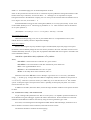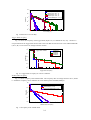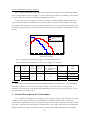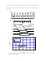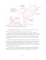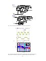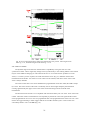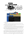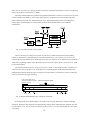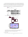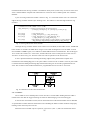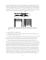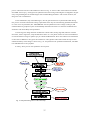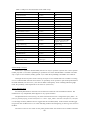
1
Production Readiness Review
ATLAS MDT TDC Chip (AMT)
Review Date : June. 20, 2002
V1.0c June. 27, 2002
V1.1 Feb. 14, 2004
Yasuo Arai
KEK, National High Energy Accelerator Research Organization
Institute of Particle and Nuclear Studies
[email protected], http://atlas.kek.jp/tdc/
1
Contents
1.
INTRODUCTION
3
2.
REQUIREMENTS AND SPECIFICATIONS
4
2.1
2.2
2.3
2.4
3.
MDT Front-end S y s t e m
Requirements to the AMT
Radiation tolerance requirements
Architecture Study with Simulations
4
5
9
10
CIRCUIT DESCRIPTION & PERFORMANCE
15
3.1
3.2
3.3
3.4
3.5
3.6
3.7
3.8
3.9
3.10
3.11
3.12
3.13
3.14
4.
DESIGN VERIFICATION & TEST
4.1
4.2
4.3
4.4
4.5
5.
Design Flow & Design F i l e s
Function Tests
Time Resolution and Non-Linearity
P o w er Consumption
Summary of Tests and Known Problems
36
39
40
41
41
46
Gamma-ray Irradiation (TID)
Neutron Irradiati o n
Proton Irradiation (SEE)
46
46
48
QUALITY CONTROL AND PRODUCTION SCHEDULE
6.1
6.2
16
21
22
24
25
26
27
29
29
30
31
32
33
34
36
RADIATION TEST
5.1
5.2
5.3
6.
Fine Time Measurement
Coarse Counter
Channel Buffer.
Vernier Encoder
L1 Buffer.
Trigger Interface & Trigger FIFO
Trigger Matching.
Encoded trigger and resets signal
Serial Readout
Error monitoring.
CSR Registers
JTAG Port.
ASD control through JTAG
LVDS Receiver/Driver
Quality Control
Procurement and Production Schedule
48
48
48
7.
SUMMARY
49
8.
REFERENCES
50
2
1 . Introduction
A TDC with sub-nano second resolution is required to obtain the necessary spatial resolution of the
Monitored Drift Tubes (MDT). The high rates expected in the ATLAS detector requires that the TDC is
capable of continuously accepting new hits while selectively extracting hits related to a trigger after the first
level trigger latency. To do this several levels of data buffering is required to keep up with the trigger rates and
hit rates expected in the experiment. In addition, high density and low-cost, low power consumption are
required in the TDC.
The TDC was named as AMT (ATLAS Muon TDC), and brief summary of the development history is
shown in Table. 1.
Table. 1. Brief summary of the history of TDC LSI development
Year
Activities
1990
First TDC LSI was developed (TMC1004, CMOS 0.8 µm) at KEK.
1994
TDC for the SSC exp. was developed (TMC304, CMOS 0.5 µm) at KEK
1996
Collaboration with CERN microelectronics group on the architecture study for the ATLAS TDC, and
requirements document were written [1].
1998
A quick test chip (AMT-0, CMOS 0.7 µm) was developed and produced at CERN.
1999
A test element chip (AMT-TEG, CMOS 0.3 µm) was developed at KEK.
PLL and radiation torelance of the process were tested.
2000
A first prototype chip (AMT-1, CMOS 0.3 µm) was developed。
2001
Muon front end electronics Preliminary Design Review.
Mezzanine boards with ASD-Lite and AMT-1 are developed and used in H8 beam test.
Second prototype chip (AMT-2, CMOS 0.3 µm) was developed.
2002
Mezzanine board with ASD-8 and AMT-2 are developed and tested at Univ. of Michigan.
Production Readiness Review.
In 1996, architecture study was done in collaboration with CERN microelectronics group, and intensive
Verilog simulations were done. Basic requirements on the AMT chip were documented in ATLAS note
(MUON-NO-179 [1]) and presented at LEB97 workshop[2]. In 1998, AMT-0 [3] was designed in a 0.7 µm
full custom CMOS process based on the 32 channel TDC designed at CERN for the quick test of front-end
electronics and MDT chambers.
On the other hand, it was decided to use a 0.3 µm CMOS Gate-Array process (Toshiba Co.) for a final
production. To develop and test many critical elements in the 0.3 µm process, a TEG (Test Element Group)
chip (AMT-TEG) was designed, fabricated and tested successfully at KEK [4, 5]. Then AMT-1 chip was
developed. AMT-1 chip mainly consists of analog part of the AMT-TEG and logical part of the AMT-0. In
February, 2001, Preliminary Design Review of the MDT front-end electronics was held and the AMT design
was approved for final design with a few recommendations [6].
Mezzanine boards which implement AMT-1 and ASD-Lite chips are produced for 10k channel (~400
boards) test of MDT detector in 2001. They are used in the H8 beam test in September 2001. Although there
were several troubles with electrical noise, DAQ hang up etc., more than 13 M events were acquired[7].
In parallel with the AMT-1 test, next version of the AMT chip (AMT-2) was designed and developed. It
implements new low-power LVDS receivers to reduce power consumption. In addition, minor bugs were
3
fixed, testability is increased, and a JTAG control circuit for the ASD. Furthermore, clock timing within the
chip was carefully adjusted. Recently a new mezzanine board which implements AMT-2 and ASD-8 chips are
produced and being tested at Univ. of Michigan and many other places.
During these development, preliminary radiation test had been done to the AMT-TEG, AMT-1, and we
got a feeling that the gate-array process has adequate radiation tolerance. Then we have done gamma and
proton irradiation test to the AMT-2 chip following ATLAS standard test method.
2 . Requirements and Specifications
2.1 MDT Front-end S y s t e m
Block diagram of the MDT front-end electronics is shown in Fig. 1. Three ASD (Amp-Shaper-Discri)
chips [8] and one AMT chip are mounted on a small multi-layer printed circuit board (mezzanine board, Fig.
2), which plugs into a MDT end plug PCB (signal hedgehog board).
Two modes of operation will be provided in MDT measurement. In one mode the ASD output gives the
time over threshold information, i.e. signal leading and trailing edge timing. The other mode measures
leading edge time and charge (pulse width). The Wilkinson ADC serves as a time slew correction and also
provides diagnostics for monitoring chamber gas gain. It operates by creating a gate of ~20ns width at the
leading edge of the signal, integrating charge onto a holding capacitor during the gate, and then running
down the hold capacitor at constant current (the maximum rundown time is of order 200ns). The
discriminator also generates artificial dead time of ~800 ns to avoid multiple hits.
Fig. 1 MDT front-end electronics. AMT chip receives timing signal from three ASD chips and sends data to a
CSM.
4
Fig. 2. Mezzanine-Lite Board Layout. The TDC chip will be mounted with 3 ASD chips.
2.2 Requirements to the AMT
We summarize the requirements to the AMT in this section. Although some parameters were changed
in past 6 years, most of the requirements discussed in reference [1] are still valid.
Number of channels per chip
There are about 370,000 MDT tubes in total. Since the number of tube layers is 3 and 4, and the ASD
chip will have 8 channels per chip, a 24 channel TDC matches well this configuration. In total 16,000 chips
and some spare chips are required for the MDT.
TDC Clock
A TDC clock with the same frequency as the bunch crossing rate must be used. In this way the coarse
time count can be correlated directly with the bunch count. In some internal parts of the TDC, such as the
PLL or the serial interface, a 2 times higher clock frequency (80 MHz) is used to improve performance. A
high speed clock in this case is phase locked to the beam clock.
Time Resolution
The resolution of one single MDT has to be better than 80 µm. During the development of the AMT
chip, the baseline gas of the MDT was changed to Ar/CO2 93/7. This gas causes the non-linearity of the rtrelation and a longer drift time (tmax ~ 800 ns). Although the requirements to the time resolution was a little
bit relieved, a timing resolution of better than 1 ns is sustained and ~300 ps resolution is foreseen in the
AMT.
Detection of Masked Hits and Shared Hits
The signal from a round drift tube has a long tail. A second track might therefore be masked by the
signal tail of a preceding track. The existence of a preceding hit can be detected by checking the data before the
trigger matching region. This masked hit information can be sent out with one word per event using a flag bit
for each channel.
5
Since the drift time of the MDT tubes is longer than the minimum interval between two triggers, some
hits may be shared by several triggers. This is illustrated in Fig. 3 where some hits are shared for event N and
N+1. Randomly accessed memory is therefore required instead of a FIFO for the first level buffer to handle
shared data.
Fig. 3. Mask & Matching window and a shared hit.
Time Measurement and Pipeline Processing
The maximum hit rate in a wire is estimated to be 400 kHz while most of wire has less than 100 kHz
hit rate. Inefficiency due to the buffer overflow of the AMT must be negligible compared with detector
inefficiency.
The timing of both leading and trailing edge of the hit signal can be stored as a pair to enable a pulse
width measurement to be performed. Optionally the leading edge only or the trailing edge only (or both
independently) time measurement can be performed in case the pulse width measurement is not required.
The signal path from the trigger and hit inputs to the readout contains several buffers so multiple events
can be processed at the same time as shown in Fig. 4. One trigger in the process of being received, One event
in the process of being trigger matched and a third event in the process of being read out.
Fig. 4. Processing of several events in parallel.
6
Bunch Counter and Coarse Counter
There are 3,564 clock periods per LHC beam revolution. Bunch crossings are identified with a 12 bit
Bunch Crossing Identifier (BCID) [9]. To correctly identify hits within the bunch structure a 12 bit coarse
time counter is required in the TDC.
Trigger Interface
When a trigger signal is given to the first level buffers, measurements related to that event must be
extracted from the buffer and sent to the data acquisition system. Main trigger conditions given from ATLAS
group are following;
• maximum level 1 trigger rate is 75 kHz (100 kHz in future upgrade)
• level 1 trigger latency is around 2.5 µs
• minimum interval between two triggers is 125 ns
Each event accepted by the first level trigger is identified by a 24 bit event ID at the system level. At the TDC
a reduced event ID of 12 bits is used.
Input and Output Signal Level
It is of vital importance that noise from digital signals on the front-end board is kept to an absolute
minimum so the small analog signal from the tubes are not corrupted. LVDS (Low Voltage Differential
Signaling, IEEE 1596.3) signals are used for all connections to/from the TDC which are actively running
while taking data.
Data Packet and Output Band width
Data packets of 32 bit are used in the serial data stream. The first four bits of the packet are allocated to
a type identifier which specifies the type of data. The following four bits are allocated for a TDC chip
identifier. This ID is used just for confirmation of the connection. Since maximum number of TDC per
chamber is 18, actual TDC ID is added to data at the CSM. Event data from different events can be separated
by the optional use of a header and a trailer.
The header contains the event ID and bunch ID of the event being readout. The trailer contains the event
ID and a word count. All required information from a hit: type identifier, TDC ID, channel ID, leading edge
time plus pulse width are contained in one 32 bit word. The conditional mask flags for the 24 TDC channels
are also contained in a single 32 bit word. In case a TDC have detected an internal error condition (e.g. buffer
overflow) it sends a special error status packet for all events which may have been affected by the error.
Hit data selected by a trigger is transferred from the TDC to the CSM (Chamber Service Module) located
outside the detector. The distance from the TDCs to the CSM is of the order of 10 meters. The connection
from the TDCs to the CSM is performed on serial links of 40 Mbits/s (optionally 80 Mbits/s is selectable
for future upgrade).
At a 400 kHz hit rate per TDC channel and a trigger matching window of 800 ns, an average of 6 hits
per TDC is expected at highest rate locations. For each hit, 36 bits (32 bits data + start bit + 2 stop bit +
parity) must be transferred from a TDC to the CSM. With a trigger rate of 100 kHz this requires an average
serial bandwidth of 32 Mbits/s per TDC including the header, trailer and a mask word.
7
Serial Link Protocol
A coding scheme of the serial data is the two wire signaling scheme. Two protocols and two clocking
schemes are prepared. One protocol is the DS protocol ( IEEE P1355 ) which keeps the required bandwidth to
an absolute minimum. Another one is simple data and clock pair (data is latched at clock edge). This requires
higher bandwidth in the link but simplify the receiving circuit. Present CSM module (CSM-0) are using this
simple data and clock pair mode. As for the clocking, there are two options; continuous clock and gated clock.
To limit the number of cables in the detector it is not considered to have a back propagation signal from
the DAQ to the TDC telling it to stop sending data in case buffers in the DAQ system are running full.
Instead buffer full flag is added to data if the buffer overflow occurs and the TDC must be capable of
recovering event synchronization locally without any higher level intervention from the DAQ system.
System setting and debugging.
The fact that the TDC is going to be embedded inside the detector requires special attention on
monitoring and in system testing capabilities. The cause and place of hardware failures must be detectable
without opening the detector such that the effect of a hardware failure can be minimized and such that a repair
can be performed fast and effectively. A relatively slow bi-directional communication path is also necessary to
be capable of loading setup and calibration parameters before data taking and to monitor the system during
operation.
The standard IEEE 1149.1 JTAG protocol is used for this purpose. The use of full boundary scan
enables efficient testing of TDC module failures while located in the system. Testing the functionality of the
chips themselves are also supported by JTAG. To insure fast and effective testing of embedded memory and
data path structures in the TDC chip special scan path registers is implemented for this.
Power Consumption
The chip will be mounted in a Farady cage at the end of MDT chamber. Therefore low power
consumption is required. Power consumption around 10 mW/ch is a target value.
Specification Summary
Specifications of AMT chip is summarized in Table. 2.
8
Table. 2 AMT Specifications (System clock frequency is 40 MHz)
• Least Time Count
• Time Resolution
• Dynamic range
0.78125 ns/bit (leading and trailing edges)
0.78-100ns/bit (width)
RMS = 300 ps (leading and trailing edges)
RMS = 300ps ~ 29ns (width)
17 bit (leading and trailing edges)
8 bit (width)
• Max. Trigger Latency
16 bit (51 µsec)
• Int./Diff. Non Linearity
• Difference between channels
• Stability
• Ring oscillator frequency
• No. of Input Channels
• Level 1Buffer depth
• Read-out Buffer depth
• Trigger Buffer depth
• Data output
Max = +/-80 p s
Maximum one time bin
< 0.1 LSB (3.0 - 3.6 V. 0 - 70 ˚C)
Input clock frequency x 2
24 Channels
256 words
64 words
8 words
LVDS Serial (10 - 80 Mbps)
or 32 bit parallel.
10, 20, 40, and 80 Mbps with DS or edge strobe.
3 bit serial control line
~5 n s
400 kHz per channel
100 kHz
Low Voltage Differential Signaling (LVDS)
Internal 100 Ohm termination.
16 control and 6 status registers.
accessed through JTAG or 12 bit control bus.
116 pins.
13 VDD pins and 14 VSS pins
3.3+-0.3V (~360 mW)
0 - 85 Deg. Cent
• Serial Output
• Serial Control (trigger and resets)
• Double Hit Resolution
• Max. Hit rate
• Max. trigger rate
• Hit Input Level
• CSR registers
•Number of I/O pins
• Number of Power/GND pins
• Supply Voltage
• Temperature range
• Process
• Number of Gate
• Package
0.3 µm CMOS Sea-of-Gate (Toshiba TC220G)
die size: 6 mm x 6 mm
110 k gates (36.2 % usage)
0.5 mm lead pitch, 144 pin plastic QFP
2.3 Radiation tolerance requirements
AMT chip is used at the end of MDT chamber, so the chip must have adequate radiation tolerance.
ATLAS group determined the policy on radiation tolerant electronics [10]. Below we briefly describe the
required radiation tolerance level to AMT.
Total Ionizing Dose
Radiation Tolerance Criteria (RTC) is calculated from Simulated Radiation Level (SRL) as following
equations.
RTC = SRL•SFsim•SFldr•SFlot
Here,
SFsim : Represents safety factor for SRL inaccuracies.
SFldr : Represents safety factor for low dose rate effects.
SFlot : Represents safety factor for the variation of radiation tolerance from lot to lot and within a lot.
9
SFldr is '1' if accelerated aging tests at elevated temperature are done.
SFlot for the pre-selection of COTS will be '2' if the final chips are produced in homogeneous batches. If the
batches of the chip is unknown, we must use SFlot = 4. Although it is not impossible to request
homogeneous batch to the fabrication company, the cost of chip will be increased. Since the radiation level is
not so high in our case, we use SFlot = 4.
Simulated Radiation Levels for total ionizing doze (SRLtid) is 0.75 Gray/year (accuracy 1%) for worst
location MDT (Endcap 2) at 1034 luminosity[10], and SFsim is '3.5'. Thus maximum value of the RTCtid
for 10 years operation is;
(RTCtid)max = 0.75 (Gray) x 3.5 x 1 x 4 x 10 (years) = 105 Gray = 10.5 krad
Non-Ionizing Energy Loss
NIEL(Non-Ionizing Energy Loss) test on pure CMOS devices is not required from ATLAS, since
CMOS devices are naturally tolerant to displacement damage.
Single Event Effects
Particles traversing the chip may introduce single event effect (SEE). Especially single event upsets
(Soft SEUs) will accidentally change the state of a memory element in the TDC. The effect of such an event
should be detected by the TDC, so parity bits are prepared in data buffers and control registers. Soft SEUs rate
can be calculated as follows;
Soft SEUf = (Soft SEUm / ARL) x (SRLsee / 108 s) x SFsim
Where,
"Soft SEUf" is the foreseen rate of soft SEU in a given location.
"Soft SEUm" is the total number of soft SEU measured in proton beam tests.
"ARL" is the Applied Radiation Level.
"SRLsee" is the simulated Radiation Level in 10 years.
"SFsim" is the safety factor of the simulation, and is '5'.
Maximum value of the SRLsee is seen in Endcap 1 region and is 8.31 x 10⁹ h/cm2/y (for hadrons
energy > 21 MeV) [11]. Average value of the SRLsee weighted by number of channels in each position is
2 x 10⁹ h/cm2/y. There are 11,360 bits memory in a AMT chip, so in total there are 2 x 108 bits in MDT
system. To keep the single event upset rate less than 1 upset/day (or 200 upsets/year), SEU cross section
must be less than 10-15 cm-2.
In addition to the SEU, destructive SEEs (such as latch up) should be avoided or some special care must
be taken.
2.4 Architecture Study with Simulations
To get a feeling of the performance of a TDC in a real system, it is required to perform simulations of
the architecture using hits and trigger signals with realistic characteristics. Several simulations of the TDC
architecture under different conditions were done by using the Verilog simulator [2] in 1996.
Since then, several changes have been happened in MDT detector and AMT design, simulations are redone to check the correctness of the architecture, and results are shown below.
The baseline simulation conditions are the following:
10
•
•
•
•
•
•
•
•
•
•
•
•
•
•
100 and 400 kHz hit rate (2/3 random hits and 1/3 correlated hits (4 hits))
100 kHz trigger rate (minimum separation is 125 ns)
drift time = 0 ~ 800 ns
pair (leading edge and width) mode measurement.
pulse width = 10 ~ 200 ns
dead time = 800 ns (generated by ASD)
trigger latency = 2.5 µs
mask & matching windows = 800 ns
search window = 1000 ns
reject offset = 3.5 µs
both header and trailer words are read out (enable_header=1, enable_trailer=1)
a mask word is read out if exist (enable_mask=1)
Speed of the serial readout is 40Mbps.
disable data rejection when trigger fifo is full (enable_trfull_reject=0)
The distribution of the hit and the trigger has exponential distributions, and one third of the hit generate
4 channel hits at a same time to emulate a jet. Block diagram of the AMT buffers are shown in Fig. 5.
Detailed explanation of the AMT circuit is available in next chapter.
We have done simulations for 3 cases of buffer control.
Case A : No hit rejection when the readout FIFO become full (enable_rofull_reject = 0)
Case B : Hit rejection when the readout FIFO become full (enable_rofull_reject = 1) and L1 buffer
occupancy become nearly full (enable_l1full_reject =1).
Case C : Hit rejection as soon as the readout FIFO become full (enable_rofull_reject = 1,
enable_l1full_reject =0).
Simulation for 80 Mbps serial speed was also done in some case.
Fig. 5 Block diagram of the AMT buffers.
11
Channel buffer occupancy
There are two locations (4 words) to store a pair measurement in a channel buffer. If the two locations
are full when new hit arrives, the new hit will not be saved in the channel buffer. However, in the MDT
condition, 800 ns dead time are introduced by the ASD. Since it takes only 650 ns (2 + 24 clock cycles) to
move all pair measurements to the L1 buffer, there is no possibility for the hit rejection at the channel buffer.
This is also confirmed with several millions of hit simulations. We never observed channel buffer occupancy
more than one.
To see the channel buffer occupancy, we have also done simulation for leading and trailing edge mode.
This will double the data rate inside the AMT chip. Fig. 6 shows the channel buffer occupancy at 400 kHz hit
rate (that is 800 kHz edge rate). Occupancy in the figure means number of remaining hits in the channel buffer
when a new hit arrives. Occupancy equal 4 means the new hit can not be written and rejected. For 1 million
simulated hits, the average occupancy is 0.25 and we have not yet seen hit with occupancy equal 4.
10
10
Probability
10
10
10
10
10
10
0
400kHz (ave.=0.25)
-1
-2
-3
-4
-5
-6
-7
0
1
2
3
Channel buffer occupancy
4
Fig. 6 Channel buffer occupancy in leading and trailing edge mode at 400 kHz hit rate.
First level buffer occupancy
The average level 1 buffer occupancy when not taking into account the processing time of trigger
matching and ASD dead-time can be calculated as:
24 ×
TriggerLatency (2.5µs) + Mask Window (800 ns)
= 7.9 ( @100KHz)
Hit Interval (10 µs)
The simulated first level buffer occupancy is shown in Fig. 7. Average occupancy at 100 kHz hit rate is 7.5
and agrees well in the expected value. At 400 kHz hit rate buffer overflow will occur due to the bandwidth
limit of the serial output. When the hit rejection at matching circuit is enabled, the buffer occupancy drops
from above 192 words where the data rejection will start in case B. The buffer occupancy drops around 50
words in case C.
12
10
10
Probability
10
10
10
10
10
0
100kHz Hit(ave.=7.5)
400kHz A(ave.=27.4)
400kHz B(ave.=26.6)
400kHz C(ave.=24.6)
-1
-2
-3
-4
-5
-6
0
50
100
150
200
250
Level 1 buffer occupancy
Fig. 7. Occupancy of the level 1 buffer. Level 1 buffer length of the AMT chip is 256.
Trigger Search time
Fig. 8 shows the time needed to search for all hits corresponding to a trigger. At the 100 kHz hit rate,
the average search time is 0.18 µs. However the maximum time will increase to around 16 µs when the hit
rate goes up to 400 kHz due to the buffer overflow (case A, B). Since the maximum time range of the AMT
is 51.2 µsec, care must be taken not to cross this limit. In case C, the trigger search time is greatly reduced to
less than 3 µsec..
10
Probability
10
10
10
10
10
0
100kHz Hit(ave.= 0.18)
400kHz A,B(ave.=0.62)
400kHz C(ave.=0.45)
-1
-2
-3
-4
-5
0
2
4
6
8
10
Trigger search time[
12
14
16
µs]
Fig. 8. Trigger search time for 100 kHz and 400 kHz hit rates.
Event Delay
Time needed from the trigger to the readout (event delay) is shown in Fig. 9.Maximum event delay will
be more than 100 µs if the hit rejection at the matching circuit is disabled (case A). The distribution will drop
at 90 µs in case B. In case C, the event delay is drops at near 70 µsec.
13
10
100kHz(ave.=5.1 µs)
400kHz A(ave.=28.6 µs)
400kHz B(ave.=21.6 µs)
400kHz C(ave.=20.4 µs)
400kHz,80Mbps(ave.=4.8 µs)
-1
10
Probability
0
10
-2
10
-3
-4
10
-5
10
0
20
40
60
80
100
120
140
Event Delay[ µs]
Fig. 9 Distribution of event delay.
Trigger FIFO occupancy
Fig. 10 shows the occupancy of the trigger FIFO (depth is 8). At 100kHz hit rate, only 1 location is
occupied. However the trigger FIFO become full if the event data rate become close to the readout bandwidth
(case A, B). In case C there are enough locations remains.
10
Probability
10
10
10
10
10
0
Trigger Rate=100kHz
100kHz Hit
400kHz A
400kHz B
400kHz C
-1
-2
-3
-4
-5
0
1
2
3
4
5
6
7
8
Trigger FIFO occupancy
Fig. 10. Trigger FIFO occupancy for various conditions.
Readout FIFO occupancy
Fig. 11 shows occupancy of the readout FIFO. The occupancy does not change much for case A, B and
C. Instead the occupancy can be reduced if the serial readout speed is doubled (80Mbps).
10
Probability
10
10
10
10
0
100kHz Hit(ave.=1.49)
400kHz Hit(ave.=13.7)
400kHz Hit,80Mbps(ave.=2.54)
-1
-2
-3
-4
0
10
20
30
40
Readout FIFO occupancy
Fig. 11 Occupancy of the readout FIFO.
14
50
60
Number of Matched Hit and Rejection Ratio
Fig. 12 shows the distribution of number of hits matched with a trigger. For 100 kHz and 400 kHz hit
rate, an average number of hits per trigger is 1.77 and 5.8 hits/trigger respectively. Probability of the masked
hit word existed is 0.77 and 0.99 for 100 kHz and 400kHz respectively.
In total, there are 4.54 words and 8.79 words per a trigger in average including a header, a trailer and a
mask words for 100 kHz and 400 kHz hit rate respectively. Table. 3 summarize these numbers. The column
of rejected hit ratio indicates the ratio of rejected hit to matched hit. Case A will minimize the rejected hit but
has relatively long event delay. On the other hand case C has shortest event delay but the rejected hit ratio will
increase.
10
Probability
10
10
10
10
10
0
100kHz
(ave.=1.77, mask=0.77)
400kHz
(ave.=5.80, mask=0.99)
-1
-2
-3
-4
-5
0
5
10
15
20
25
Number of hits per trigger
Fig. 12. Number of matched hits per trigger for 100 and 400 kHz hit rate.
Table. 3 Summary of simulation for 1 million hits (trigger rate = 100 kHz)
Hit Rate
Buffer
Control
Case
100 kHz
No. of
Hits
per trig
No. of
Mask word
per trig
1.77
0.77
No. of words per
trig
(incl. header, trailer
and mask)
4.54
A
400 kHz
B
5.80
0.99
8.79
C
Rejected Hit
ratio
Maximum
Even
Delay
0%
40 µsec
0.2%
130 µsec
0.4%
90 µsec
0.6%
70 µsec
Summary
We see AMT has enough buffer length and readout bandwidth for 100 kHz hit rate. As for 400 kHz hit
rate, buffer overflow will occur occasionally and event delay will increase if there is no hit rejection
mechanism. By rejecting very small fraction of the data when many hits comes in a very short time, we can
keep event delay to less than 70 µsec.
3 . Circuit Description & Performance
Fig. 13 shows a block diagram of the AMT chip. The hit signal coming from the ASD chip via LVDS
is used to store the fine time and coarse time measurement in individual channel buffers. The fine time
measurement is obtained from 16 taps of a asymmetric ring oscillator which is stabilized with a Phase Locked
Loop (PLL). The coarse time measurement is obtained from a 13 bit counter. The timing of both leading and
trailing edge of the hit signal can be stored as a pair to enable a pulse width measurement to be performed.
15
The time measurements from the channel buffers are stored during the first level trigger latency in a
common level 1 buffer. First level triggers converted into trigger time tags and a corresponding event ID are
stored temporarily in a trigger FIFO waiting to be matched with the hit measurements from the first level
buffer. Hits matching triggers are written into a readout FIFO waiting to be transferred to the DAQ system
via a serial link.
The architecture of the AMT is also described in several documents [12, 13] in detail.
Fig. 13 Block Diagram of the AMT chip.
3.1 Fine Time Measurement
Asymmetric Ring Oscillator
An asymmetric ring oscillator is used to obtain sub-ns timing resolution. Fig. 14 shows a simplified
schematics and its timing diagram of the asymmetric ring oscillator. It only shows 8 stages but the actual
chip implements 16 stages. The asymmetric ring oscillator creates equally spaced even number (16) of timing
16
signals. To keep the equally spacing, each buffers are located in a circular (rectangular) shape as shown in Fig.
15.
Actual signal was observed with oscilloscope and shown in Fig. 16. We see the rising edge timing is
aligned in a line.
(c)
250
f_PLL(MHz)
200
Sim (worst)
Sim (typ)
Sim (best)
measurement
150
100
80MHz
50
0
0.0
0.5
1.0
1.5
2.0
2.5
3.0
Vg[V]
Fig. 14 (a) Asymmetric ring oscillator, (b) timing signal in each nodes, (c) Oscillation
frequency vs. Control voltage (Vg).
17
Fig. 15 Layout of the asymmetric ring oscillator. Signals propagate as shown in arrow. The
size is about 300 µm by 100 µm.
Fig. 16. Output waveform of the asymmetric ring oscillator.
Phase Locked Loop
Schematics around the Phase Locked Loop (PLL) circuit is shown in Fig. 17. Main parts are a
frequency divider, a phase frequency detector (PFD), a charge pump, a loop filter (LPF), and a voltagecontrolled oscillator (VCO; asymmetric ring oscillator in this case). An external capacitor (Cvg) is required in
the loop filter.
18
Fig. 17 Schematics of PLL and Ring Oscillator in AMT-2.
The frequency divider is selected from 1:1, 1:2, 1:4 and 1:8, and 1:2 is used in ATLAS. The control
voltage is split into 2 lines (VGN1 and VGN2) to control oscillation start and stop.
Fig. 18 shows relation between internal clock and external clock for both AMT-1 and AMT-2. In
AMT-1, there are two flip flops (F1 and F2) to divide the 80 MHz clock to 40 MHz clock, each output is used
in the PFD and internal clock generation respectively. We occasionally experienced half cycle (12.5 ns) phase
shift between external clock and the internal clock. It is caused when reset is not asserted after power on or
external clock is disappeared temporally. To avoid this shift, only 1 flip flop is used to divide the 80 MHz
clock in AMT-2.
Although the chip is designed in a gate-array technology, layout of the time critical parts such as PLL
and the asymmetric ring oscillator were designed manually to achieve high accuracy. We measured the jitter of
the PLL circuit by measuring the oscillation period of each cycle (Fig. 19 (a)). RMS values of the jitter
versus frequency and power supply voltage are plotted in Fig. 19 (b). The jitter of the PLL is small (~ 150 ps)
and stable for the 40-120 MHz frequency range and for supply voltages between 2.6 - 3.6 V (normal operating
condition is 80 MHz and 3.3V respectively).
We observed PLL lock process in AMT-TEG. Fig. 20 show the output of ring oscillator and control
voltage during lock process. An external capacitor of 6800 pF is connected to the Vg pin. Time constant of
the charge up and down is relatively long and it will take several hundreds micro sec to become stable.
19
Fig. 18 PLL and Internal clock generation in (a) AMT-1 and (2) AMT-2.
(a)
(b)
Vdd[V]
2.5
300
2.7
2.9
3.1
3.3
3.5
250
3.7
3.9
vs Fosc
vs Vdd
Jitter[ps]
200
150
100
Operating Point
50
0
0
20
40
60
80
Fosc[MHz]
100
120
140
Fig. 19 Waveform of the input clock and PLL oscillation. PLL jitter is measured relative to
the input clock. (b) Stability of the PLL vs. oscillation frequency and supply voltage.
20
Fig. 20 VCO output and control voltage (Vg) during PLL lock process. Above figure starts
from Vg = 0 V, and bottom figure starts from Vg = 3.3 V.
3.2 Coarse Counter
The dynamic range of the fine time measurement is expanded by storing the state of a clock
synchronous counter. The hit signal may though arrive asynchronously to the clocking and the coarse counter
may be in the middle of changing its value when the hit arrives. To circumvent this problem two count
values, 1/2 a clock cycle out of phase, are stored when the hit arrives (Fig. 21). Based on the fine time
measurement from the PLL one of the two count values will be selected, such that a correct coarse count
value is always obtained.
The coarse counter has 13 bits and is loaded with a programmable coarse time offset (the LSB is always
0) at reset. The coarse counter of the TDC is clocked by the two times higher frequency than the bunch
crossing signal thereby the upper 12 bit of the coarse counter becoming a bunch count ID of the
measurement.
The bunch structure of LHC is not compatible with the natural binary roll over of the 12 bit coarse time
counter. The bunch counter can therefore be reset separately by the bunch count reset signal and the counter
can be programmed to roll-over to zero at a programmed value. The programmed value of this roll-over is also
used in the trigger matching to match triggers and hits across LHC machine cycles. Coarse counter was
successfully tested to run at 120 MHz (Fig. 22).
21
Fig. 21 Phase shifted coarse counters loaded at hit.
Fig. 22. Coarse Counter test at 120 MHz.
3.3 Channel Buffer.
Each channel has a small buffer where measurements are stored until they can be written into the
common on-chip level 1 buffer. The channel buffer is implemented as a FIFO and can contain two complete
time measurements (leading and trailing edge) as show in Fig. 23.
The channel buffer is controlled such that it is capable to measure the minimum pulse width of ~10 ns.
To measure the pulse width of the hit signal a time measurement pair consisting of a leading and a trailing
edge is assembled. The leading and trailing edge measurements can be performed as separate measurements
written into a common buffer and then paired at the output of the channel buffer. The channel buffer also
works as 4 word buffer for leading and trailing edge measurement mode.
If a hit occurs when the channel buffer is full, it will be not be saved and no time measurement will be
performed, although the loss of hits due to overflow of the channel buffer is extremely small as shown in
section 2.4 . The information of the rejected hit should be transferred to next valid hit ('enable_rejected' = 0).
Instead the information of the rejected hit can be transferred as soon as the channel buffer is available
('enable_rejected' = 1).
In this case the time of the data is the time when the buffer is available and not
actual data. The information of the rejected hit is reported by 'E' flag of a data word in edge measurement.
22
Since there is no location of 'E' flag in the data word of pair (combined) measurement, an error word insertion
will be used if the error information is needed.
When the channel buffer have performed the required measurements a request to be written into the clock
synchronous first level buffer is issued. This request signal is synchronized to avoid possible meta-stable
states and then processed by the channel arbitration logic. When paired measurements of a leading and a
trailing edge is performed the two measurements are taken off the channel buffer as one combined
measurement.
Fig. 23 The channel buffer control scheme.
When several hits are waiting to be written into the level 1 buffer an arbitration between pending
requests is performed. A registered arbitration scheme illustrated in Fig. 24 is used to give service to all
channels equally. Each channel have a hardwired priority but new requests are only allowed into the arbitration
queue when all pending requests in the queue have been serviced. The request queue is serviced at a rate equal
to the clock frequency.
The time measurements are not written into the level 1 buffer in strict temporal order. A request to be
written into the first level buffer is not made before the corresponding pulse width measurement has been
finalized and the channel arbitration does not take into account which hit occurred first. This have important
effects on the following trigger matching.
Load request register when
all previous requests in register
have been serviced
Highest priority
Channel to write into buffer
Hardwired priority encoder
Lowest priority
Request register
Ch. 0 Ch. 1
• • •
Ch.22 Ch.23
Fig. 24 Registered hardwired priority arbitration of channels.
Recording speed of the channel buffer is important to have a good double pulse resolution and edge
separation. Minimum edge separation was determined by reducing pulse width and pulse separation until the
hit information is lost. Fig. 25 shows an example of short pulses. Two pulses are measured in a pair mode
successfully.
23
The data transfer speed from the channel buffer to the L1 buffer is measured by changing the number of
simultaneous hit channels and determining the minimum hit interval where all hits are accepted. In Fig. 26
minimum hit interval for N channel simultaneous inputs are plotted. Above the data point all hit information
is recorded, but if the hit interval is reduced less than the data point, a part of the hit information become lost
due to the lack of the transfer capability. The line in the figure shows expected speed from the circuit. We
confirmed the overhead for arbitration is only 2 cycle and successive data transfer occurs at each cycle.
Fig. 25 Waveform and data display of short pulses recorded in the AMT chip.
T
Channel Buffer
50ns + 25ns x Nch
Ch 1
Level 1 Buffer
Ch 2
•••
Ch N
Hit Interval T [ns]
600
All hit accepted
400
T = 50ns + 25ns x Nch
200
Part of hit lost
0
0
4
8
12
16
20
24
No. of Hit Channels N
Fig. 26 Minimum hit interval for simultaneous hit inputs. System clock cycle is 25 ns. The
data points show minimum hit intervals and the straight line indicates the expected
performance from the 2 cycles plus N cycles required by the design.
3.4 Vernier Encoder
When a hit has been detected on a channel the corresponding channel buffer is selected, the time
24
measurement done with the ring oscillator is encoded into binary form (vernier time), the correct coarse count
value is selected and the complete time measurement is written into the L1 buffer together with a channel
identifier.
A part of Verilog code for the encoder is shown in Fig. 27. The encoder checks 4 bits set to find clock
edge of the ring oscillator instead of just checking 2 bits. This reduces to catch false edge within the ring
oscillator.
assign # 1
// minimum 4 bit width, (MSB) ---0011--- (LSB)
edge_detect[15:0] = {vernier[14:0],vernier[15]} & vernier[15:0] &
~{vernier[0], vernier[15:1]} & ~{vernier[1:0], vernier[15:2]},
fine_bin[3]
fine_bin[2]
fine_bin[1]
fine_bin[0]
= | edge_detect[15:8],
= ( | edge_detect[15:12] ) | ( | edge_detect[7:4] ),
= ( | edge_detect[15:14] ) | ( | edge_detect[11:10] ) |
( | edge_detect[7:6] ) | ( | edge_detect[3:2] ),
= edge_detect[15] | edge_detect[13] | edge_detect[11] | edge_detect[9] |
edge_detect[7] | edge_detect[5] | edge_detect[3] | edge_detect[1];
Fig. 27 Verilog code for the vernier encoder.
Although the ring oscillator and the coarse counter runs at 80 MHz, the base LHC clock is 40 MHz and
bunch number is counted at 40 MHz. Most of logics in the AMT are designed to run at 40 MHz. To shift
from 80 MHz to 40MHz regime, we would like to define different name to measured time. We call the upper
12 bit of the coarse counter as a ‘coarse time’, and the LSB of the coarse counter plus the vernier time as a
‘fine time’ as shown in Fig. 28. Thus the coarse time will be equivalent to the bunch count.
In case a paired measurement of leading and trailing edge has been performed the complete time
measurement of the leading edge plus a 8 bit pulse width is written into the L1 buffer. The 8 bit pulse width
is extracted from the leading and trailing edge measurement taking into account the programmed roll-over
value. The resolution of the width measurement is programmable from 0.78 ns/bit to 100 ns/bit.
Fig. 28. Definition of coarse time and fine time.
3.5 L1 Buffer.
The L1 buffer is 256 words deep and is written into like a circular buffer. Reading from the buffer is
random access such that the trigger matching can search for data belonging to the received triggers.
In case the first level buffer runs full, the hit measurements from the channel buffers will be discarded.
A special buffer overflow detection scheme takes care of handling the buffer overflow condition and properly
marking events which may have lost hits.
When the first level buffer only have space for one more hit ( full -1 ) and a hit measurement arrives
25
from the channel buffers, the hit is written into the buffer together with a special buffer full flag. After this
the buffer is considered full and following hits are discarded. When 4 measurements have been removed from
the buffer by the trigger matching ( full - 4) and a new hit arrives, the buffer full status is cleared and the hit is
written into the buffer with the buffer full flag set. This situation is illustrated in Fig. 29 where the two hits
with the buffer full flag set is shown. These two hits define a time window where all hits have been discarded
and this is used in the trigger matching to detect if an event potentially have lost some hits.
(a)
full T
recover T
Time
Events
Events with overflow data
overflow flag
(b)
1
0
(c)
full T
coarse time
0
coarse time
1
recover T
1
full T
0
coarse time
Fig. 29 First level buffer overflow handling. (a) Events of which matching time overlap with
the period of overflow are marked. (b) Full time mark in the first level buffer. (c) Recover time
mark.
3.6 Trigger Interface & Trigger FIFO
The trigger interface takes care of receiving the trigger signal and generate the required trigger time tag
and event number to load into the trigger FIFO.
The basis for the trigger matching is a trigger time tag locating in time where hits belong to an event of
interest. The trigger time tag is generated from a counter with a programmable offset. When a trigger is
signaled the value of the bunch counter (trigger time tag) is loaded into the trigger FIFO (see Fig. 30).
In case the trigger FIFO runs full, triggers are rejected and complete events from the TDC are
potentially lost. This would have serious consequences for the synchronization of events in the readout of the
TDC. A full flag in the trigger FIFO together with the event number of the triggers are used to detect the loss
of triggers and to make sure that the event synchronization in the readout is never lost. If a positive trigger is
signaled when the trigger FIFO is full the trigger interface stores the fact that one ( or several ) triggers have
been lost. As soon as the trigger FIFO is not any more full the event number of the latest lost trigger is
written to the FIFO together with a trigger lost flag. The trigger matching can then detect that triggers have
been lost when it sees the trigger lost flag. The trigger matching can also in this case determine how many
triggers have been lost by comparing the event number of the previous trigger and the current event number
stored together with the trigger FIFO full flag. This scheme is illustrated in Fig. 30 where it can be seen that
triggers for event 11,12,13,14 have been lost. For each lost trigger the trigger matching will generate
“empty” events ( header + trailer ) marked with the fact that it contains no hits because the trigger was lost.
26
Fig. 30. Trigger FIFO and overflow handling.
3.7 Trigger Matching.
Trigger matching is performed as a time match between a trigger time tag and the time measurements
them selves. The trigger time tag is taken from the trigger FIFO and the time measurements are taken from
the L1 buffer. Hits matching the trigger are passed to the read-out FIFO.
Fig. 31. Trigger latency and trigger window related to hits on channels. There are 3 time
counters ; coarse time, trigger time and reject time counters.
A match between the trigger and a hit is detected within a programmable time window (Fig. 31). The
trigger is defined as the coarse time count (bunch count ID) when the event of interest occurred. All hits from
this trigger time until the trigger time plus the matching window will be considered as matching the trigger.
The trigger matching being based on the coarse time means that the “resolution” of the trigger matching is
one clock cycle (25 ns) and that the trigger matching window is also specified in steps of clock cycles.
The search for hits matching a trigger is performed within an extended search window to guarantee that
all matching hits are found even when the hits have not been written into the L1 buffer in strict temporal
order.
To prevent buffer overflow and to speed up the search time an automatic reject function can reject hits
older than a specified limit when no triggers are waiting in the trigger FIFO. A separate reject counter runs
with a programmable offset to detect hits to reject.
The trigger matching can optionally search a time window before the trigger for hits which may have
masked hits in the match window. A channel having a hit within the specified mask window will set its mask
flag. The mask flags for all channels are in the end of the trigger matching process written into the read-out
27
FIFO if one or more mask flags have been set.
In case an error condition (L1 buffer overflow, Trigger FIFO overflow, etc.) has been detected during the
trigger matching a special word with error flags is generated. All data belonging to an event is written into the
read-out FIFO with a header and a trailer. The header contains an event id and a bunch id. The event trailer
contains the same event id.
The search for hits in the first level buffer, matching a trigger, can not be performed in a simple
sequential manner for several reasons. As previously mentioned the hits are not guaranteed to be written into
the first level buffer in strict temporal order. In addition a hit may belong to several closely spaced triggers. A
fast and efficient search mechanism which takes these facts into consideration is implemented using a set of
memory pointers and a set of programmable time windows;
Write pointer:
Memory address where new hit data is written.
Read pointer:
Memory address being accessed to look for a time match.
Start pointer:
Memory address where search shall start for next trigger.
Mask window:
Time window before trigger time where masking hits are to be found.
Matching window:
Time window after trigger time where matching hits are to be found.
Search window:
Time window specifying how far the search shall look for matching hits.
(extends searching range to compensate for the fact that hit data are not perfectly
time ordered in the first level buffer).
The pointers are memory addresses being used during the search as illustrated in Fig. 32 and the
windows are measures of time differences from the trigger time to the time of the leading edge of the hit
signal.
The trigger matching search starts from the location pointed to by the start pointer. When the first
masked hit or matched hit is found the start pointer is set to the new location. The search continues until a hit
with a coarse time younger than the search limit has been found or there is no data in the buffer. The start
pointer is also incremented while data rejection is being done.
The trigger matching can optionally be programmed to reject matched hits when the read-out FIFO is
full. This rejection can be made conditional on the fact that the first level buffer is more than 3/4 full. This
option will prevent event data to pile up inside the TDC. Event data that have piled up inside the TDC will
take very long time before arriving to the second level buffers in the DAQ system. Here they will probably be
discarded as they arrive to late. In case the TDC is not programmed to reject matched hits, the trigger
matching function will stop when the readout FIFO is full and the l1 buffer and the trigger FIFO will start to
fill up.
28
Fig. 32 First level buffer pointers and time windows.
3.8 Encoded trigger and resets signal
Four basic signals are encoded using three clock periods (Table 1). The simple coding scheme is
restricted to only distribute one command in each period of three clock periods. A command is signaled with a
start bit followed by two bits determining the command. When using encoded trigger and resets an additional
latency of three clock periods is introduced by the decoding compared to the use of the direct individual trigger
and resets.
Table 1 Encoded signal bit pattern.
Meaning
Trigger
Bunch count reset
Global reset
Event count reset
bit|
210
100
110
101
111
3.9 Serial Readout
All accepted data from the TDC can be read out via a serial read-out interface in words of 32 bits. The
event data from a chip typically consists of a event header, accepted time measurements, mask flags, error
flags (if any error detected for event being read out) and finally a event trailer.
The accepted TDC data can be transmitted serially over twisted pairs using LVDS signals. Data is
transmitted in words of 32 bits with a start bit set to one and followed by a parity bit and 2 stop bit (Fig. 33).
The serialization speed is programmable from 80 to 10 Mbits/s. In addition to the serialized data an LVDS
pair can carry strobe information in a programmable format.
Leading Strobe: Direct serializing clock to strobe data on rising edge.
DS Strobe :
DS strobe only changes value when no change of serial data is observed.
Fig. 33 Serial frame format with start bit and parity bit (leading strobe mode).
29
Fig. 34 LVDS Serial output waveform for DS strobe mode at 40 Mbps.
Data read out from the TDC is contained in 32 bits data packets. The first four bits of a packet are used
to define the type of data packet. The following 4 bits are used to identify the ID of the TDC chip
(programmable) generating the data. Only 7 out of the possible 16 packet types are defined for TDC data. The
remaining 9 packet types are available for data packets added by higher levels of the DAQ system. Some of
the data format are shown in Fig. 35. Full description is available in the Users Manual [12]
TDC header: Event header from TDC
31 30 29 28 27 26 25 24 23 22 21 20 19 18 17 16 15 14 13 12 11 10 9
1 0 1 0
TDC ID
Event ID
8
7
6 5 4
Bunch ID
3
2
1 0
TDC trailer: Event trailer from TDC
31 30 29 28 27 26 25 24 23 22 21 20 19 18 17 16 15 14 13 12 11 10 9
1 1 0 0
TDC ID
Event ID
8
7 6 5 4
Word Count
3
2
1 0
Mask flags: Channel flags for channels having hits with in mask window
31 30 29 28 27 26 25 24 23 22 21 20 19 18 17 16 15 14 13 12 11 10 9
0 0 1 0
TDC ID
Mask flags
8
7
6
5
4
3
2
1 0
7
6
5
4
3 2 1 0
Fine Time
Combined measurement: Combined measurement of leading and trailing edge
31 30 29 28 27 26 25 24 23 22 21 20 19 18 17 16 15 14 13 12 11 10 9 8 7 6
0 1 0 0
TDC ID
Channel
Width
Coarse Time
5
4
3 2 1 0
Fine Time
Single measurement: Single edge time measurement
31 30 29 28 27 26 25 24 23 22 21 20 19 18 17 16 15 14 13 12 11 10 9 8
0 0 1 1
TDC ID
Channel
T E
Coarse Time
T: Edge type. E: Hit error.
Fig. 35 Data format of the output data packet.
3.10 Error monitoring.
There are two kinds of error; hard errors and temporal errors. Hard errors are enabled with enable_error
bits (CSR12[8:0]) and read through error_flags (CSR16[8:0]). Temporal errors are not a real error but
represent information of buffer overflows.
30
Hardware Errors
All functional blocks in the TDC are continuously monitored for error conditions. Memories are
continuously checked with parity on all data. All internal state machines have been implemented with a “one
hot” encoding scheme and is checked continuously for any illegal state.
The JTAG instruction register have a parity check to detect if any of the bits have been corrupted during
down load. The CSR control registers also have a parity check to detect if any of the bits have been corrupted
by a Single Event Upset (SEU). The error status of the individual parts can be accessed via the CSR status
registers (Table. 4) or reported in a error word.
Table. 4. Hardware Errors
Error flag
bit#
Description
Coarse count error
0
A parity error in the coarse count has been detected in a channel
buffer.
Channel select error
1
A synchronization error has been detected in the priority logic used
to select the channel being written into the L1 buffer. (more than 1
channel are selected)
L1 buffer error
2
Parity error detected in L1 buffer.
Trigger FIFO error
3
Parity error detected on trigger FIFO.
Matching state error
4
Illegal state detected in trigger matching logic.
Read-out FIFO error
5
Parity error detected in read-out FIFO.
Read-out state error
6
Illegal state detected in read-out logic.
Control parity error
7
Parity error detected in control registers.
JTAG error
8
Parity error in JTAG instruction.
Temporal Errors
Temporal errors are embedded in data and available only through an error word and shown in Table. 5
Table. 5. Temporary Errors
Error flag
bit#
Description
L1 buffer overflow
9
L1 buffer becomes full and hit data have been lost
Trigger FIFO overflow
10
Trigger fifo becomes full and events have been lost
Readout FIFO overflow
11
Readout fifo becomes full and hit data have been lost
Hit error
12
A hit measurement have been corrupted (channel select error or
coarse count error)
3.11 CSR Registers
There are two kinds of 12 bits registers, "CONTROL" and "STATUS" registers. The "CONTROL"
registers are readable and writable registers which control the chip functionality. The "STATUS" registers are
read only registers which shows chip statuses.
There are 16 Control registers (CSR0-15) and 6 Status registers (CSR16-21). These registers are
accessible through 12bits bus and JTAG interface (Fig. 36). Bit assignments for the "CONTROL and
"STATUS" registers are shown in Table. 6 and Table. 7 respectively. Detailed explanation of these bits are
available in AMT User's manual [12].
31
Table. 6. Bit assignment of the control registers.
11
10
9
8
CSR0 global_re error_ disable_ enable_
set
reset
encode errrst_
bcrevr
CSR1
CSR2
CSR3
CSR4
CSR5
CSR6
CSR7
CSR8
CSR9
strobe_select
readout_speed
CSR10
CSR11
CSR12
enable_
auto_
reject
enable_
rofull_
reject
enable_
sepa_
readout
CSR13
CSR14
CSR15
7
test_
mode
BIT
6
test_
invert
5
4
enable_ disable_
direct ringosc
3
2
clkout_mode
mask_window
search_window
match_window
reject_count_offset
event_count_offset
bunch_count_offset
coarse_time_offset
count_roll_over
width_select
error_
tdc_id
test
enable_ enable_ enable_ enable_ enable_ enable_ enable_ enable_ enable_
l1occup match
mask relative serial
header
trailer rejected
pair
_readout
enable_ enable_ enable_ inclk_ enable_ enable_ enable_ enable_ enable_
l1full_ trfull_ errmark boost ermark_ errmark l1ovr mreset_ resetcb_
sepa
code
_detect
rejected _ovr
reject
reject
enable_ enable_
enable_
sepa_
sepa_
error
bcrst
evrst
enable_channel[11:0]
enable_channel[23:12]
general_out[11:0]
1
0
pll_multi
enable_ enable_
trailing leading
enable_ enable_
mreset_ setcount
_bcrst
evrst
Table. 7. Bit assignment of the status registers (read only).
CSR16
CSR17
11
rfifo_
empty
l1_
empty
CSR18
tfifo_
empty
CSR19
coarse_
counter
[0]
10
9
8
rfifo_ control_
full
parity
l1_
l1_
l1_
nearly_ over_
over
full
recover
flow
tfifo_ running
tfifo_
full
nearly_
full
tfifo_
occupancy
CSR20
CSR21
7
6
5
4
3
error_
flags
l1_
write_address
2
1
l1_
read_address
l1_
start_address
coarse_counter[12:1]
general_in
0
0
rfifo_
occupancy[5:0]
3.12 JTAG Port.
JTAG (Joint Test Action Group, IEEE 1149.1 standard) boundary scan is supported to be capable of
performing extensive testing of TDC modules while located in the system. Testing the functionality of the
chip itself is also supported by the JTAG INTEST and BIST capability. In addition special JTAG registers
have been included in the data path of the chip to be capable of performing effective testing of registers and
embedded memory structures. Furthermore, it is also possible to access the CSR registers from the JTAG
port.
Structure of JTAG circuit within the AMT chip is shown in Fig. 36, and implemented commands are
shown in Table. 8.
32
0
Fig. 36. Structure of JTAG - CSR registers.
Table. 8 JTAG Instructions.
Instruction Code
Name Description
0000:
EXTEST. Boundary scan for test of inter-chip connections on module.
0001:
IDCODE. Scan out of chip identification code.
0010:
SAMPLE. Sample of all chip pins via boundary scan registers.
0011:
INTEST. Using boundary scan registers to test chip itself.
0100 - 0111:
(not used)
1000:
CONTROL. Read/Write of control data.
1001:
ASD control. (AMT-2 only)
1010:
STATUS. Read out of status register information.
1011:
CORETEST. Read/Write internal registers for debugging.
1100:
BIST. Built In Self Test for Memories.
1101:
General purpose output port (AMT-2 only)
1110:
(not used)
1111
BYPASS. Select BYPASS register.
3.13 ASD control through JTAG
Design of the ASD requires an external JTAG to serial controller [14] to access internal registers of the
ASD. Original plan is to use a FPGA device in the mezzanine board. Since the AMT already have JTAG
controller, we decided to include the interface in the AMT-2 chip (Fig. 37).
Simulated timing diagram is shown in Fig. 38. Unfortunately both chip has TDO register, so 2 TDO
registers are connected serially at the end of the scan chain. Thus the scan chain looks 1 additional scan
register.
33
ASD1
D
Q
C
ASD0
dac[3]
Scan Cell
dac[2]
Scan Cell
dac[1]
Scan Cell
AMT-2
shadow reg
ASDOUT
tdi
load
TDO reg
tdo
Q
D
Scan Cell
Q
dac[0]
C
ASDLOAD
ASDIN
D
TDO reg
data_in
C
shift reg
1
0
Q
D
data_out
Q
D
Q
S
tms
tck
trstb
ASDDOWN
down
ASDCLK
clk
C
C
Fig. 37. AMT-2 - ASD control simulation model. There are 2 TDO registers at the end of scan
chain. Therefore there looks 1 additional scan register exist in the chain.
ASDOUT
ASDDOWN
ASDCLK
ASDLOAD
ASDIN
Fig. 38. Simulated timing diagram of the ASD control signals. There is one additional bit is
seen in yellow circle location.
3.14 LVDS Receiver/Driver
LVDS receivers are used in clock receiver, encoded control signals and hit input receivers. Required
speed of the receiver in the clock and the encoded signals are 40 MHz. As for the hit inputs, higher than 100
MHz bandwidth is required to receive less than 5 ns pulse. Fig. 39 shows pulse measurement for 100 MHz
clock in the LVDS receiver. Clock of 100 MHz are successfully received in the receiver.
Power consumption of LVDS receiver used in the AMT-1 was rather large (15.5 mW), but this was
very much reduced in AMT-2 (4.5 mW) by designing a new LVDS receiver. Simulation results of DC current
and propagation delay are shown in Fig. 40. The power consumption is reduced to less than 1/3 of previous
34
design. Furthermore the propagation delay is also reduced a factor of 3.
The specification of the LVDS receiver and driver are shown in Fig. 41.
Fig. 39 LVDS receiver waveform measurement at 100 MHz. Change of duty factor of the
output is mainly caused by the boundary scan registers and the output driver.
7
6
(a)
∆Vin=100mV
Old
Idd[mA]
5
4
3
2
New
1
0
0.0
0.5
1.0
1.5
Vicm[V]
2.0
2.5
6
Tpd[ns]
5
(b)
Old
4
Tpd(LH)
Tpd(HL)
3
New
2
1
0
0.0
0.5
1.0
1.5
Vicm[V]
2.0
2.5
Fig. 40 (a) DC current comparison between old and new LVDS receiver. (b) Propagation delay
comparison between old and new LVDS receiver.
35
Fig. 41 LVDS Receiver and Drivers specifications.
4 . Design Verification & Test
4.1 Design Flow & Design F i l e s
Simplified design flow of the AMT chip is shown in Fig. 42. Analog Simulations of macro cells such
as PLL circuits and LVDS driver/receiver are studied with HSPICE simulator. Then Verilog models of the
macro cells are built to incorporate the simulation results into Verilog environment. Created user macros and
Mega cells used in the design are summarized in Table. 9.
Table. 9 User Macro and Mega Cells used in the AMT.
Cell Kind
Cell Name
Comment
User Macro
WMMP16
16 bit channel buffer
User Macro
WMND4P
4 inputs symmetric NAND for PLL circuit
User Macro
WMRTMC
Asymmetric Ring Oscillator
User Macro
WLVDSINR1
LVDS receiver with 100 ohm resister
User Macro
WLVDSOUT
LVDS driver
Mega Cell
AI8036A
36 bit x 256 words dual port memory (L1 buffer)
Mega Cell
FI3028A
28 bit x 8 words FIFO (trigger FIFO)
Mega Cell
FI6030A
30 bit x 64 words FIFO (readout FIFO)
Then register transfer level modules are ported from AMT-0 [3] design and modified to fit to our design.
To understand the Verilog code of the AMT-0, many block diagrams and state diagrams are created in this
36
process. The block structure of the modules are shown in Fig. 43. Source codes of the AMT-2 are available
from PRR web site [15]. Actual gates are synthesized from the Verilog codes and gates are mapped to the gate
array. The generated gates are simulated again with estimated delay parameters. After several iterations, the
design was sent to manufacture.
At the manufacture, they insert BIST logics, then all gates and macro's are placed and routed. During
this process clock trees which meets timing requirements of the chip are automatically generated and inserted
in to the circuit. In placement, PLL and WMRTMC cells are placed near control voltage (VGN) pin, and
channel buffers are grouped in a place. Extracted delay information are back to us from the manufacture and
simulation with actual delays were performed.
At final stage, the design has been verified with Toshiba VSO (Verilog Sign-Off) software. It checks
drive limit, electro migrations, setup and hold times and so on. Test pattern used in IC testers at manufacture
are converted from Verilog test patterns [16] to Toshiba standard format. Worst case and best case simulations
are also done in addition to the typical case simulations. Then glitches and conflict within the chip are also
checked. Summary of the design is shown in Fig. 44. Test pattern for DC parameter measurement, I/O buffer
tests and BIST test are also prepared.
In reality, above process were repeated in various points.
Fig. 42 Simplified design flow of the AMT chip.
37
Fig. 43 AMT-2 chip Verilog module structure.
Module name
:
amt2_chip
Series name
:
TC220G
TC220G Library date : 991008
User's id
:
arai
Array type
:
T3S47
TC220G Library version : 2.14
Number of input pins
(excluding bidirectional pins) --------:
Number of output pins
(excluding bidirectional pins) --------:
Number of bidirectional pins -----------------------------------:
----Total number of I/O signal pins used ---------------------------:
Number of pad locations used for input pins -------------------:
Number of pad locations used for output pins -------------------:
Number of pad locations used for bidirectional pins ------------:
----Total number of pad locations used for above -------------------:
Total number of pad locations available for above --------------:
Number of I/O slots
Number of I/O slots
Number of I/O slots
Number of I/O slots
----Total number of I/O
Total number of I/O
for
for
for
for
116
74
26
16
116
160
input buffers --------------------:
output buffers --------------------:
bidirectional buffers -------------:
internal buffers ------------------:
126
30
16
14
slots used for above -----------------------:
slots available ----------------------------:
186
316
Number of redundant cells ( deleted ) --------------------------:
62
Normal
cell
-----Number
Number
Number
Number
used
used
used
used
74
26
16
Normal
IO
SMC
block block block
Total
------ ------ ------ -----of cell types used -----------:
of cell used -----------------:
of transistor pairs used -----:
of gates used ----------------:
117
5
11637
7
69615 112990
37854 69700
15
95
216
143
0
0
0
0
137
11739
182821
107697
Number of gates in master chip ---------------------------------:
Array gate usage (%) -------------------------------------------:
Array gate usage excluding blocks (%) --------------------------:
297680
36.18
16.61
Maximum number of pins per net ---------------------------------:
Average number of pins per net ---------------------------------:
Number of nets with 10 < pins/net <= 20 ------------------------:
Number of nets with pins/net > 20 ------------------------------:
Number of signal nets ------------------------------------------:
181
3.117
231
77
12773
Fig. 44 Summary of AMT-2 chip.
38
4.2 Function Tests
Many test patterns are created during the design. Purpose of the test patterns can be classified into 3
categories.
(1) Check logical design : test patterns in this category are created in early stage. Logical function of the
design are checked.
(2) Check gate timings : test patterns in this category are used to verify the logic synthesis, place and
rout result. Any glitch, conflict, and setup/hold timing violations are checked.
(3) Chip production check : test patterns in this category are used mainly in LSI testers at the
manufacture. The purpose of this test is verifying the wafer process and the chip was produces as
designed. Therefore test pattern should activate all nodes and gates. IDDS, I/O buffer and BIST
tests are also classified in this category.
Prepared test patterns of category (3) is summarized in Table. 10 and summary of test pattern coverage
is shown in Fig. 45. Those patterns are available from PRR web site [16]. Toggle check coverage is 99.06%.
Most of non-activated nets belongs to un-used gates.
Table. 10 Summary of test patters for production test.
Name
Contents
fn1
CSR read/write test and coarse counter test.
fn2
Hit test 1
fn3
Hit test with serial readout
fn4
Hit test with parallel readout
fn5
JTAG test 1
fn6
Hit test with no trigger matching
fn7
Encoded control input test
fn8
Error Test。
fn9
Internal test with Core registers
fn10
Channel buffer full test
fn11
Level 1 buffer full test
fn12
JTAG Test 2 and boundary scan test
fn13
Hit Test 2
pll
PLL oscillator stability test
idds
I/O buffer DC test and IDDS measurement
hiz
Output buffer Hi impedance test.
st
bist
Toshiba standard test circuit test for input buffers.
BIST test for memories.
39
SELECTED TOGGLE FILES AND RESULTS
Top module name
: amt2_chip
Input toggle check results file(s)
AMT2.tg.fn1
AMT2.tg.fn2
AMT2.tg.fn3
AMT2.tg.fn4
AMT2.tg.fn5
AMT2.tg.fn6
AMT2.tg.fn7
AMT2.tg.fn8
AMT2.tg.fn9
AMT2.tg.fn10
AMT2.tg.fn11
AMT2.tg.fn12
AMT2.tg.fn13
AMT2.tg.idds
AMT2.tg.hiz
AMT2.tg.pll
AMT2.tg.st
AMT2.tg.bist
Number of total nets
= 12921
Number of toggle
= 25842
'0' and '1' activated nets = 12677
'0' activated nets
= 108
'1' activated nets
= 136
Non-activated nets
= 0
Toggle check coverage
= 99.06 (%)
Fig. 45 Summary of Test pattern coverage.
4.3 Time Resolution and Non-Linearity
Time resolution was measured by supplying a clock synchronous hit signal to the input and varying the
delay time of the signal. The result is shown in Fig. 46. The RMS value of 300 ps is obtained.
Non-linearity of the time measurement was measured by applying a hit signal for which the delay time
is uniformly distributed, and counting the number of hits recorded in each bin. The Differential Non-Linearity
(DNL) and Integral Non-Linearity (INL) are shown in Fig. 47 (a) and (b) respectively. Both are small enough
(RMS < 70 ps) for our purpose.
400
RMS=300 ps
Counts
300
200
100
0
-2
-1
0
1
2
∆t[ns]
Fig. 46 Time resolution measurement. Input clock frequency is 40 MHz and time bin is
781.25 ps/bit. The data contains digitization error of 225 ps.
40
DNL[ns]
0.4
(a)
Max=+/-0.14ns, RMS=0.06ns
0.2
0.0
-0.2
INL[ns]
0.4
(b)
Max=+/-0.13ns, RMS=0.07ns
0.2
0.0
-0.2
0
5
10
15
TDC count
Fig. 47 (a) Differential non-linearity, and (b) Integral non-linearity measurement.
4.4 Power Consumption
Power consumption of the AMT-1 and AMT-2 chip was measured at 100 kHz hit rate for 24 channels
and 100 kHz trigger rate. The results are;
AMT-1 : 3.3V x 240 mA = 800 mW/chip (~33mW/chan)
AMT-2 : 3.3V x 110 mA =360 mW/chip (~15mW/chan)
Power consumption in different conditions are shown in Fig. 48.
40
-18mW
20
AMT-2
100kHz Trig
100kHz Hit
Start
40MHz Clk
30MHz Clk
20MHz Clk
10MHz Clk
0
100 Ohm T
10
LVDS Only
Power(mW/ch)
AMT-1
30
Fig. 48 Power consumption of the AMT-1 and AMT-2 for various conditions.
4.5 S ummary of Tests and Known Problems
Although it is difficult to list all the test items done, major test items are summarized in Table. 11. We
found several bugs in AMT-2. Detail of each error is described in following sections. These bugs will be fixed
before the mass production.
41
Table. 11 Major test item and results of the AMT-2 chip.
Test Item
Status
Result
Time Resolution
Tested
OK
Double Pulse Resolution
Tested
OK
Leading and/or Trailing edge mode
Tested
OK
Pair mode measurement
Tested
OK
Channel buffer overflow
Tested
minor bug
L1 buffer overflow
Tested
OK
Trigger FIFO overflow
Tested
OK
Readout FIFO overflow
Tested
OK
Encoded Control Circuit
Tested
OK
Serial I/O
Tested
OK
JTAG I/F
Tested
OK
ASD Control
Tested
minor bug (an extra TDO
register, section 3.13 )
Trigger Matching
Tested
major b u g
Mask Readout
Tested
OK
Error Reporting
Tested
minor bug
Power Consumption
Tested
OK
CSR Read/Write
Tested
OK
PLL
Tested
OK
Mezzanine board test
(Cosmic Ray Test)
Tested at Univ. of
Michigan
see Tiesheng Dai's Report
Beam Test
This Summer
Channel Buffer Overflow
When a hit is rejected in channel buffer, there are two way to report the rejection. One is force rejection
('enable_rejected' =1) in which a rejected flag is reported as soon as the channel buffer is available. The other
way is report in next valid hit ('enable_rejected' =0) in which the rejected flag is attached to next valid hit.
Although the force rejection works correctly, the report in next valid hit does not work due to a timing
error in a channel buffer controller. Since there is no possibility of hit rejection in pair mode operation due to
the ASD dead-time (see section 2.4 ), this does not affect to data quality. Even in leading and trailing edge
mode, the possibility of the rejected hit is less than 10-6 (section 2.4 ).
Trigger Matching Error
We found a phenomena in which hits will be missed or a false hit will be matched in AMT-2. The
mechanism is very complicated, and it happens in very special situation.
The phenomena will occur (see Fig. 49) if the time between two hits is longer than 'reject_offset + 52
µsec' (or precisely saying, 52 usec+104 µsec x N < Time - reject_offset < 104 usec+104 µsec x N, 104 µsec
is a full range of AMT), and there are two triggers after the second hit (Hit2). In this situation second trigger
(Trig2) will miss the Hit2 even if it is within matching window. Interesting thing is that Trig1 will not miss
the Hit2.
The source of error is miss-count of start pointer and an old hit will remain in the L1 buffer. Sometime
42
this old hit will change to young hit if half cycle of time range passes, and blocks actual hits. In another time,
this old hit accidentally match to the next trigger, and appear as a false hit.
Fig. 49 Timing relation when the hit miss occur. Waveforms at point A, B, C and D are
shown in following figures.
Fig. 50 shows the registers around L1 buffer and trigger matching circuit. Read address counter gives
address of the L1 buffer. The contents of the addressed data is latched in data register and the read address is
stored in output address register. The data is checked in trigger matching circuit. There are 2 functions in the
trigger matching circuit. One is matched hit search which is functional when a trigger arrives from trigger
FIFO. Another function is old hit rejection. This function is always enabled except the matched hit search
period.
If the trigger matching circuit find an old hit, the address is stored in start address counter, and the read
address counter is loaded with the start address at the end of the triggered event. We follow the signals from
Fig. 51 to Fig. 54. In these figure 'n742' signal indicate 'load_data*' signal.
Fig. 50 Block diagram around L1 buffer and Trigger matching circuit.
43
Fig. 51 Signal timings around the point A (matching hit search) .
In this Fig. 51, address '0' contains an old hit, and address '1' contains a matched hit. After this process,
start_address has a correct value of '1'.
Fig. 52 Signal timings around the point B (old hit rejection).
Then after some time (Fig. 52), the data in address '1' become old, so output_data_address (out_data_adr)
is incremented to '2'. However the start_address still points address '1'. Here the start_address should also be
incremented to '2'.
Although the start_address points wrong address, the trigger matching proceeds correctly if next hit
comes within 52 µsec, since the data in address '1' is rejected anyway.
44
Fig. 53 Signal timings around the point C (Trig 1).
Then assume there is no hit in more than 52 µsec and a first trigger (Trig1) arrives (Fig. 53). Since the
out_data_adr is pointing new hit address of '2', this trigger can find correct hit (Hit2). However, at the end of
the process, the read address and out_data_adr is backed to '1'. The reason why the hit miss does not occur for
Trig1 is that the read_address is loaded at the end of matching process.
Fig. 54 Signal Timings around the point D (Trig 2).
At second trigger (Trig2), the out_data_adr points address '1' which has a data more than half cycle ago.
Trigger matching circuit subtract reject_count from the data (hit_tag) and judge from the sign bit, so the
judgment of the address '1' data is 'too young'. Thus the search will stop and could not find a hit in address '2'.
Fixing this error is very simple, jus 1 flip-flop is needed in the load_start_address signal.
45
Error Reporting
Hardware error reporting within event data does not function as expected. When the reporting is enabled
(enable_errmark = 1), an error word is inserted to events occasionally. Since the hardware error will seldom
occur, and it can be checked through JTAG at the beginning and end of run. This function is not mandatory.
The reason of the malfunction is still under investigation.
5 . Radiation Test
Radiation test results are documented in different material; " AMT-2 TID Test Report" [17] and
"AMT-2 SEE Test Report" [18]. These tests were done following the ATLAS standard test method, and there
was no severe effects in the AMT chip under estimated conditions. Some other results obtained in other test
are shown below.
5.1 Gamma-ray Irradiation (TID)
In ATLAS standard test method, we have not seen any damage to the AMT-2 up to 20 krad, while total
dose expected for worst location of the MDT electronics is 10.5 krad(Si) for 10 years LHC operation. Here we
show other test results especially on the effect to the transistor parameter with gamma irradiation.
Gamma-ray irradiation test was done at Tokyo Metropolitan University with a Co60 source. The
irradiation rate was about 90 rad(Si)/sec, and total dose irradiated was 100 krad(Si). During the irradiation so
called worst bias conditions for MOS transistors ( 3.3 V is applied to NMOS gate, and no voltage is applied
to PMOS gate), were used. To study post-radiation effects, parametric measurements were also done after
annealing (1 week at 100 degree C) following the MIL-STD-883 method [19].
In a sub-micron process, most severe damage from the ionization process is an increase of leakage
current. Fig. 55 shows drain leak current for NMOS and PMOS transistors. An increase of NMOS drain leak
current above 25 krad(Si) was seen while no increase is seen in PMOS. Recovery of the pre-radiation
condition is seen after the annealing in NMOS.
Threshold voltage shifts of transistors are shown in Fig. 56. There is no shift seen in PMOS transistors
and a NMOS transistor while small shifts (~100 mV) are seen in two NMOS transistors. Since these
transistors do not have any protection circuit, the transistors are susceptible to damage. More samples are
needed to confirm whether the shift is due to the irradiation or not.
Fig. 57 shows variation of oscillating frequency of a ring oscillator and supply current. The ring
oscillator is composed of 33 NAND gates. The oscillating frequency becomes lower above 50 krad(Si). The
total chip current was also increased above 50 krad(Si).
5.2 Neutron Irradiation
Although NIEL test is not required for CMOS chip, we have done a neutron irradiation test at the
PROSPERO reactor facility in France on April 1999. Eight chips were exposed to neutron flux of 1.0 x 10¹³
46
-5
10
-6
10
(a) NMOS
-7
10
-8
Id[A]
10
-9
10
-10
10
-11
Id[A]
10
-10
(b) PMOS
10
-11
10
-12
10
10
before Irrad.
Dose[krad]
100
after anneal.
Fig. 55 Drain leakage current of (a)NMOS and (b)PMOS transistors. Left-most and right-most
points show the value before irradiation and after 1 week at 100°C annealing respectively
(a) NMOS
Vth[V]
0.8
0.6
0.4
Vth[V]
-1.0
(b) PMOS
-0.8
-0.6
before Irrad.
10
100
Dose[krad]
after anneal.
150
Chip 1
Chip 2
100
Idd[A]
Osc. Freq.[MHz]
Fig. 56 Threshold voltage shifts of (a)NMOS and (b)PMOS transistors.
Chip 1+2
1.0
0.5
0.0
1
before irradiation
10
100
Dose[krad]
Fig. 57 (a) Oscillation frequency of a ring oscillator, (b) Total current of two chips. Left-most
points show the value before irradiation.
47
and four chips were exposed to 1.6 x 10¹³ n/cm2 (1 MeV neutron equivalent). During the neutron exposure,
chips are placed in a conductive plastic case. The expected neutron flux at MDT front-end electronics for 10
years of LHC operation is less than 1012 n/cm2.
After cooling of the radioactivity (~ 2 months), we measured transistor parameters and ring oscillator
frequency. We have not observed any apparent change in all sample chips.
5.3 Proton Irradiation (SEE)
Please see "AMT-2 SEE Test Report" [20]. Foreseen soft SEU rate is 6.8 x 10⁻⁶ upset/sec/MDT, and no
latch-up was observed.
6 . Quality Control and Production Schedule
6.1 Quality Control
Fig. 58 shows quality control of the gate-array process of Toshiba Co. Since AMT-2 is produced in
commercial gate-array technology, high quality is expected in general. In addition, test patterns and electrical
check will be done in the manufacture, and they provide us only good ICs which pass all the test.
Fig. 58 Quality Controll of the gate-array Process.
6.2 Procurement and Production Schedule
During a preparation for this PRR, we found a few bugs in the AMT-2, one of which is serious
although the error occurs in very limited case. On the other hand, we had to proceed procurement procedure to
get the chip until March 2003 (end of Japanese fiscal year 2002), since the procurement procedure will take
about 9 months.
Therefore we propose AMT procurement and development schedule as shown in Fig. 59. We will
proceed procurement procedure as scheduled. In parallel we will make the correction to the AMT-2 chip and
produce AMT-3 chip as soon as possible. We would like to fix all the known bugs but also try to minimize
the corrections. We may use ECO (Engineering Change Order) in which present placement and routing are
kept, and corrections are made using spare gates around the error location. We think we can get AMT-3 chips
around October. We also prepare all the necessary tools and mezzanine board until this time, so we can
quickly move to the test.
After the successful test of the AMT-3, we permit the mass production of the AMT-3 to the
manufacture. This may be possible since the date of delivery is next March, and time needed for mass
production is about 3 months. If further modifications are required to the AMT-3, we postpone the date of
delivery after March 2002 as a final means.
48
Fig. 59 Schedule of the AMT development and production.
7 . Summary
AMT LSI has been developed for the time measurement of the MDT detector. Radiation test of the chip
was done for TID and SEE, and the chip showed adequate tolerance. Many tests were done in laboratories, on
chamber and in beam test, and showed good performance. Unfortunately (or fortunately) a serious bug was
found in trigger matching circuit recently, so we need one more iteration. However, we think this iteration
can be done in parallel with procurement procedure, so mass production in next spring is still possible.
49
8 . References
[1] Y.Arai and J. Christiansen, "Requirements and Specifications of the TDC for the ATLAS Precision
Muon Tracker", ATLAS Internal Note, MUON-NO-179, 14 May 1997.
[2] Y.Arai and J. Christiansen, "TDC Architecture Study for the ATLAS Muon Tracker", Proceedings of the
Third Workshop on Electronics for LHC Experiments, London, Sep. 1997. CERN/LHC/97-60, pp315319.
[3] J. Christiansen, "AMT-0 manual", http://micdigital.web.cern.ch/micdigital/amt.htm.
[4] Y. Arai, "Performance and Irradiation Tests of the 0.3 µm CMOS TDC for the ATLAS MDT",
Proceedings of the Fifth Workshop on Electronics for LHC Experiments, Snowmass, 1999.
CERN/LHCC/99-33, pp 462-466.
[5] Y. Arai, "Development of Frontend Electronics and TDC LSI for the ATLAS MDT", 7th International
Conference on Instrumentation for Colliding Beam Physics Hamamatsu, November 15-19, 1999, Nucl.
Instr. Meth. A. Vol. 453, pp. 365-371 (2000).
[6] Report of the Preliminary Design Review on ATLAS MDT Electronics, ATC-RM-ER-0012, Feb.,
2001.
[7] Avolio, G et al., "First results of the 2001 MDT chambers beam test", ATL-COM-MUON-2001-022
[8] John Huth, John Oliver, Werner Riegler, Eric Hazen, Christoph Posch, Jim Shank, " Development of an
Octal CMOS ASD for the ATLAS Muon Detector", Proceedings of the Fifth Workshop on Electronics
for LHC Experiments, Snowmass, 1999. CERN/LHCC/99-33, pp. 436-442.
[9] Trigger and DAQ Interfaces with Front-End Systems: Requirement Document, Version 1.0, Atlas
Trigger-DAQ Steering Group, January, 1996.
[10] Atlas policy on radiation tolerant electronics, ATLAS Radiation Tolerance Criteria (Rev 2). Radiation
tables were revised on Nov. 2001. http://www.cern.ch/Atlas/GROUPS/FRONTEND/radhard.htm
[11] "ATLAS Policy on Radiation Tolerant Electronics", ATC-TE-QA-0001, July 2001, and ATLAS
Radiation Tolerance Criteria (Rev 2). Radiation tables were revised on Nov. 2001.
http://www.cern.ch/Atlas/GROUPS/FRONTEND/radhard.htm
[12] AMT-1&2 User's Manual, http://atlas.kek.jp/tdc/amt2/
[13] AMT-2 Data Sheets, http://atlas.kek.jp/tdc/amt2/
[14] Christoph Posch, "MDT-ASD: Serial data I/O and programmable parameters",
http://bmc.bu.edu/bmc/asd/octal/spec/ASD00A_Prog.PDF.
[15] AMT-2 Verilog source code, available from http://atlas.kek.jp/tdc/PRR/Verilog/.
[16] AMT-2 Verilog test patterns, available from http://atlas.kek.jp/tdc/PRR/TestPattern/.
[17] Y. Arai " AMT-2 TID Test Report", June 1, 2002, http://atlas.kek.jp/tdc/PRR/ .
[18] Y. Arai, "AMT-2 SEE Test Report", June 6, 2002, http://atlas.kek.jp/tdc/PRR/ .
[19] Test Method and Procedures for Microelectronics, MIL-STD-833, Method 1019.4.
[20] Y. Arai, "AMT-2 SEE Test Report", June 6, 2002, http://atlas.kek.jp/tdc/PRR/ .
50