1
SERBIAN JOURNAL OF ELECTRICAL ENGINEERING
Vol. 8, No. 2, 2011
FPGA implementation of a hybrid on-line process
monitoring in PC based Real-Time systems*
Bojan Jovanović1, Milun Jevtić 1
Abstract: This paper presents one way of FPGA implementation of hybrid
(hardware-software based) on-line process monitoring in Real-Time systems
(RTS). The reasons for RTS monitoring are presented at the beginning. The
summary of different RTS monitoring approaches along with its advantages and
drawbacks are also exposed. Finally, monitoring module is described in details.
Also, FPGA implementation results and some useful monitoring system
applications are mentioned.
Keywords: On-line hybrid monitoring, Real-Time systems, VHDL, FPGA.
1
Introduction
Monitoring system is the process or set of possible distributed processes
whose main function is dynamic acquisition, interpretation and participation in
information concerning application, during the application execution [1].
Therefore can be said that monitoring system improve vitality, security, fault
tolerance and adaptability of RTS. For proper functionality of RTS it is
necessary not only to give the correct results on the outputs, but to give them in
exactly defined time interval. This is especially true for hard real-time systems
(HRTS), because untimely execution of the tasks can lead to disaster. Tracking
the course of events in RTS while it running we can make conclusions about
meeting the timing requirements. Therefore, can be said with good reason that
on-line monitoring (monitoring while system is running) of processes and events
in HRTS is of enormous importance because it provides its predictable behavior.
Implementing on-line monitoring we can check the execution time of every
process/task or defined program code segments, both from upper (maximum
execution time) and lower (minimum execution time) side.
1
University of Niš, Faculty of Electronic Engineering, E-mail: {bojan,milun.jevtic}@elfak.ni.ac.rs
*Award for the best paper presented in section Electronics, at Conference ETRAN 2010, June 07-11, Donji
Milanovac, Serbia
1
B. Jovanović, M. Jevtić
2
RTS monitoring strategies
Monitoring system is intrusive if it requires the use of application resources
(CPU time, I/O devices, communication channels etc.). Monitoring systems are
mainly intrusive in some level. Completely non-invasive monitoring system use
specialized hardware designed for monitoring. Ideal monitoring system which is
completely transparent to the target system is very difficult to achieve in
practice. There are three basic approaches in implementation of RTS monitoring:
Software, Hardware and Hybrid.
Software implementation of RTS monitoring is flexible, but largely
intrusive and therefore significantly disturb RTS timing characteristics.
Hardware based approach in implementation of RTS monitoring is noninvasive in some level but requires specialized hardware. Whereas the target
system must support the possibility of its installation, the use of this approach is
inflexible and clumsy. It should be planned during the design of the target
system.
Hybrid monitoring enables both, non-invasive nature of a hardware
approach and the flexibility of a software approach. That’s why the hybrid
monitoring system is some kind of trade-off between pure hardware and pure
software monitoring approaches.
3
RT tasks and events
Total correctness of an RTS operation depends not only upon its logical
correctness, but also upon the time in which it is performed. This is especially
true for HRTS where the completion of a task after its deadline is considered
useless. Ultimately, this may cause a critical failure of the complete system.
Dasarathy gave a classification of timing constraints for a RTS [2]. In general,
there are two categories of timing constraints:
Performance constraints that set limits on the response time of a system
and
Behavior constraints that make demands on the rates at which users apply
stimuli to the system.
Checking the timing parameters of RT task and events, on-line monitoring
checks correctness of their execution.
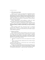
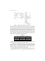
RT task τi can be characterized with the following timing parameters (Fig.
1): r – moment of occurence of the request for task execution; B – maximum
delay to the start of task execution; C – task execution time (needed CPU time);
D – time limit for task execution; T – period of occurence of periodic tasks.
2
FPGA implementation of a hybrid on-line process monitoring in PC based RT systems
Fig. 1 – Timing parameters of RT task
3.1. RT task monitoring scenarios
According to importance they have in RTS as well as according to their
timing parameters, RT tasks can be divided into pre-emptive and non preemptive tasks.
Concerning its execution time, pre-emptive tasks, unlike the non preemptive ones, do not have strict limits. Also, their possible failure in execution
would not affect significantly the proper functioning of RTS. Therefore,
scheduler can pause the execution of such tasks when receiving execution
request from some higher priority RT task. After the execution of high priority
task scheduler continues the execution of previously paused task. On the other
hand, non pre-emptive tasks execution failure, or execution outside given time
limits can lead to whole RTS failure. Because of this, high priorities are assigned
to these tasks. Furthermore, they can not be paused while running.
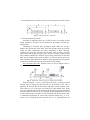
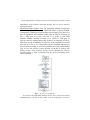
Non pre-emptive RT tasks: Possible course of non pre-emptive task (τi)
execution is shown on Fig. 2.
Fig. 2 – Monitoring scenario of non pre-emptive task execution
From the moment – event rk when request for task τi execution occured,
allowed delay to starting the task execution can be checked at first. This is
important for the tasks that do not initiate with some external interrupt event.
These tasks are „set“ in the queue for execution by some internal event. In the
case of exceeding the interval Bi , monitoring timer-counter generates a hardware
interrupt request, and error Error_B is detected. Another monitored time interval
is task execution time (CPU time). For task execution time which is shorter than
Ci (minimum required time for correct task execution), marker Error_C- is set.
In the case of exceeding the task execution time Ci + Δi (maximum time for
3
B. Jovanović, M. Jevtić
correct task execution) monitoring module generates interrupt request to detect
error Error_C+.
Such monitor performs over each RT task. Upon detection of any of these
errors, it is the policy of the planner and available time what will be taken.
Restarting of the same task or starting some alternative task (λi) execution which
will overcome given situation can be done. For each task, deadline Di for his
execution should also be monitored. Special counter-timer is most suitable for
this purpose. In the case of his exceeding, interrupt request is generated and
hardware-software security task (τsi) is started. This security task should recover
RTS or place it in a safe condition.
Pre-emptive RT tasks: Monitoring of pre-emptive tasks τi (Fig. 3) differs
from the previous monitoring scenario. While his execution is stopped because
of higher priority task τj, its monitoring timer-counter should be stopped (during
Cj).
Fig. 3 – Monitoring scenario of pre-emptive task execution
4
Hybrid on-line process monitoring module
Depending on the application and environment, timing constraints imposed
on a RTS vary widely. Here presented FPGA based monitoring module would
be applicable to each RTS determined to meet strict timing constraints imposed
by the real-world processes. FPGAs are chosen because of their low cost and
ability of reconfiguration.
4.1. General descriptions
Posing the demand that on-line monitoring do not require significant CPU
time and clumsy additional specialized hardware, this paper presents one way of
FPGA implementation of hybrid on-line RTS monitoring. It is intended for RTS
based on an industrial PC and Linux operating system which is widely accepted
and available open source system in RTS.
Implemented system monitors up to 32 processes i.e. RT tasks and events
that execute in parallel. The number of monitored processes is relatively small,
but it should be said that HRTS in industrial applications do not have a lot of
processes. However, since our monitoring module for 32 processes requires only
4
FPGA implementation of a hybrid on-line process monitoring in PC based RT systems
23% of FPGA resources, as will be seen later, number of monitored processes
can be easily expanded up to 150. The system is based on additional hardware
module with 32 programmable timer-counters and interrupt logic [3]. Each
monitored process has assigned his own timer-counter. Timers-counters are used
as devices for defining the moments of events’ time occurrence as well as
watchdog i.e. monitoring timers for checking the correct timing execution of the
processes. For minimal intrusion and using of CPU time during monitoring,
hardware module for PCs PCI slot is realized as shown on Fig. 4.
clock
FPGA device
Clr
CmdReg
OE
Data
Load
...
Data
TC
IRQ31
Load
OE
OE
Sl 3
INTR
1
1/4
1/16
1/64
Divider
INTA
1MHz
Load
16bCOUNTER
16bCOUNTER
EN
Clk
MUX
1
1/4
1/16
1/64
EN
Clk
MUX
CmdReg
Write
Read
16
DataBus
TC
INTERRUPT CONTROLLER
IRQ0 Data
INTR
INTA
Fig. 4 – PCI card with hybrid on-line monitoring module
From Fig. 4 can be seen that the interface from monitoring module to RTS
consists of the following signals: Data Bus, Read, Write, INTR, INTA, sl and clr.
DataBus is a 16 bit bidirectional bus. It transmits the data from RTS to
monitoring module and vice versa. RTS activates Read (Write) signals each time
when need to read data from (write data to) monitoring module.
Monitoring module sets INTR (Interrupt request) signal each time when any
of currently executing tasks do not execute properly or execute outside of
required time interval. As a response, RTS reads the message from Data Bus and
sets INTA (Interrupt Acknowledge) signal. Message contains information about
the interrupt nature and the ID of the task that caused interrupt. It is now
scheduler policy to determine the actions that will be taken. When receiving
Interrupt Acknowledge, monitoring module resets INTR signal and continues to
monitor RTS.
5
B. Jovanović, M. Jevtić
Sl signal is 3 bit select used by RTS when selecting the register from which
want to read data (or selecting the register to write data to). The use of this signal
will be later explained with more details.
Clr signal has a function of clear signal and it is used by RTS to reset
monitoring module.
Monitoring module is controlled by software primitives from RTS and has
the following functions:
Setting the working mode of the timers-counters,
Setting the time constraints,
Enabling the timers-counters,
Disabling the timers-counters,
Reading the timers-counters,
Timers-counters interrupt processing and
Comparison of the timers-counters state with time constraints.
During the system verification phase monitoring system provides
information about system timing characteristics and creates a log file. During the
system operation it should detect deviations from predicted timing behaviour.
These deviations could be the possible consequence of a failure in RTS.
Thereby, monitoring system has two working modes. First mode refers to the
system analysis. It performs with the purpose to measure the execution time of
every RT task. Obtained information can be used for the future control of the
RTS. In the second mode monitoring module has the function of built-in selftesting based on a watchdog function. It checks the upper and lower time limit at
the tasks and periodic and quasi-periodic events level. The activation of each
task initiates the procedure of starting his assigned timer-counter. Monitoring
timer-counter sets to previously defined maximum task execution time and starts
its countdown. If excess of the time interval happens, monitoring module sets
interrupt request. If the task is complete before time excess, timer-counter stops
its countdown with the end of task execution. Monitoring module reads its state
and checks whether the task is executed before the minimum needed execution
time. If the task is executed in regular time intervals RTS continues to work.
Otherwise, scheduler starts provided procedure for system recovery from
detected error. In this way, predicted behaviour of HRTS is ensured.
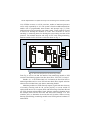
4.2. Monitoring module architecture
In monitoring module architecture we can clearly distinguish Data-path and
Control Unit. But before we describe them both separately, let’s still consider
communication interface between monitoring module and RTS. From Fig. 5 can
6
FPGA implementation of a hybrid on-line process monitoring in PC based RT systems
be seen that monitoring module communicates with RTS using four different 16
bits registers: DataRegRead, DataRegWrite, CommandReg and StatusReg. All
four registers have enable (EN) signals for activation.
Fig. 5 – Communication interface between monitoring module and RTS
DataRegRead and DataRegWrite are registers for data storage. Using
DataRegRead RTS reads data from monitoring module while using
DataRegWrite register RTS sends data to monitoring module. For sending
command to monitoring module CommandReg is used. Monitoring module
status can be read from StatusReg. To access any of these registers RTS uses
Read, Write and sl signals as shown in Table 1.
Table 1
RTS – Monitoring module communication
sl
Read
Write
Selected
register
Action
000
001
010
011
1
0
0
1
0
1
1
0
DataRegRead
DataRegWrite
CommandReg
StatusReg
Reg to DataBus
DataBus to Reg
DataBus to Reg
Reg to DataBus
Fig. 6 shows bit-level structure of CommandReg and StatusReg registers.
10 MSB bits of StatusReg are not used. StatusReg(5) stores TCmin bit.
This bit is set to 1 each time when RT task is executed faster than
minimal required time for proper task execution. The meaning of this bit
will be explained with more details when considering monitoring module
Data-path. Since module monitors up to 32 processes it is necessary
minimum 5 bits for indentify each of them. So, 5 LSB bits of StatusReg
store the identification of the RT task (process) which caused the interrupt
– Interrupt ID. Concerning CommandReg, his 5 MSB bit are not used.
7
B. Jovanović, M. Jevtić
CommandReg(10..9) bits store information about the time quantum which is
used when measuring different time intervals. This two pace bits will be
considered later. CommandReg(8..5) bits contain the code of the command while
5 LSB bits of this register address the task the command applies to.
Fig. 6 – Bit-level structures of Status and Command registers
Monitoring module Data-path: To show the whole monitoring module Data-path
on a single figure would be complicated. Therefore, Fig. 7 shows the part of the
Data-path needed for a single RT process. Each of 32 processes has the same
architecture. Data-paths of all processes are wired to 16 bits wide DataIn and
DataOut buses so they could communicate with RTS. All wires attached to
DataIn and DataOut buses are in high-impedance state except one which in this
moment uses the bus for communication. 1MHz clock and frequency divider are
common for Data-paths of all processes.
Fig. 7 – The part of the data-path needed for a single RT task
8
FPGA implementation of a hybrid on-line process monitoring in PC based RT systems
As shown on Fig. 7, single process Data-path consists of one 3 bits wide
CmdReg, one 4in1 multiplexer, one 16 bit counting-down counter, two 16 bits
wide registers for storing constants Cmax and Cmin and one RS flip-flop.
CmdReg MSB bit is used to enable/disable counter while 2 LSB bits are
attached to multiplexer select signal in order to determine counter clock
frequency (pace bits). By setting Lr to 1 CmdReg can be loaded from DataIn
bus. Similarly, by setting OEr his content is available through DataOut bus.
After reset, CmdReg content is 000. Using 1MHz clock source time quantum for
time measuring can be 1, 4, 16 or 64 µs. Accordingly, maximum time for task
execution can be 65.5, 262, 1048 or 4194 ms. It should be noted that by
changing clock source we can obtain different time quantum and different
maximum task execution times.
CmaxReg and CminReg are 16 bits registers intended for storing the
constants that determine maximum and minimum task execution time,
respectively. They are also wired to DataIn and DataOut buses so they can be
loaded through DataIn bus by setting Lmax (Lmin) or its content can be read
through DataOut bus by setting OEmax (OEmin). They are also connected to
counter.
Counter is 16 bit and of counting-down type. Its starting value can be set
either from DataIn bus (by setting Lc to 1) or from CmaxReg (by setting LCmax
to 1). Through DataOut bus his current state can be read (by setting OEc to 1).
TC bit is set to 1 when counter, counting backward, reach the zero. This means
that maximum allowed task execution time has expired. In all other counter
states TC bit is 0. Being S input of RS flip-flop, TC bit controls his TCreq
output. When TC=1, TCreq which, as will be seen later, has a direct impact to
INTR bit, is also set to 1. TCmin counter output gives us the information whether
or not minimum task execution time has expired. Since the counter can monitor
both CmaxReg and CminReg registers, it can measure time expired from task
execution beginning (Eq. 1) and compare it with minimum needed one stored in
CminReg.
expired_time=CmaxReg – counter_state
(1)
While expired time is less than minimum required task execution time
(expired_time<CminReg value), TCmin is set to 1, else to 0. After reset,
counter is in 111...111 state. The part of the monitoring module Data-path
which is common to all tasks is shown on Fig. 8. Decoder which is on the
right-hand part of the Fig. 8 is used to decode the way in which the inputs (Load,
OE, INTA and R) are connected to the outputs. This is all done using 8 bits wide
SEL signal. Load input signal can be connected on the following outputs: one of
32 different Lr signals, one of 32 different Lc signals, one of 32 different LCmax
signals, one of 32 different Lmax signals or on one of 32 different Lmin signals.
9
B. Jovanović, M. Jevtić
Fig. 8 – The part of the Data-path common to all RT tasks
OE input signal can be connected on the following outputs: one of 32 different
OEr signals, one of 32 different OEc signals, one of 32 different OEmax signals
or one of 32 different OEmin signals. INTA input signal can be connected on one
of 32 different INTAx outputs while input R can be connected on one of 32
different Rc output signals. To select which of the 32 different outputs will be
connected with the input 5 LSB bits of SEL signal are used. In the case of Load
and OE signals, since they can be connected on different types of Load and OE
outputs, 3 MSB bits of SEL signal are used to determine its connection to the
output. The way of determination is shown in Table 2.
Table 2
Load and OE signal connection protocol
SEL(7..5) bits
Load connects to
OE connects to
000
001
010
011
100
Lc
LCmax
Lr
Lmax
Lmin
OEc
OEr
OEmax
OEmin
With 32in1 multiplexer and using 5 LSB bits of SEL signal, one of the 32
different TCmin bits is connected to unique TCmin output.
32 different TCreq signals are connected to the priority coder inputs.
Priority coder gives 5 bits identification of the process that caused the interrupt.
In the case when two or more processes require interrupt, priority coder will
identify the process with the highest priority. 32 TCreq signals are also
connected to 32 inputs of OR logic gate with INTR output.
So, if maximum allowed task execution time has expired, TCreg is set to 1.
Consequently, INTR is also set to 1, and priority coder gives us the 5 bits
10
FPGA implementation of a hybrid on-line process monitoring in PC based RT systems
identification of the task that caused the interrupt. These 5 bits are stored in
Interrupt ID register.
Monitoring module Control Unit: For monitoring module Control Unit
finite state machine (FSM) is used. FSM clock source is equal to 50MHz.
Consequently, FSM moves from current to the next state every 20ns. First
part of algorithmic state mashine (ASM) chart of FSM is presented on
Fig. 9. After reset in s0 state, next state is s1. In the s1 state FSM
monitors whether interrupt occurred. If so (INTR=1) FSM goes to
Interrupt state for interrupt processing. If there is no interrupt (INTR=0),
FSM waits for the command to be received. If the command is received
next state is s2, else s1. In s2 state FSM reads the command and moves to
the next state according to received command stored into CommandReg
(Fig. 6). Pace bits from this register determine 2 LSB bits of CmdReg, thus
defining counter clock frequency. Process ID bits determine RT task the
command applies to, while 4 Command Code bits from CommandReg define
desired command.
Fig. 9 – The first part of ASM chart
In interrupt state FSM loads Interrupt ID (En ID=1) and status registers
(LoadStatusReg=1) as well as reset counter. Also, by writing 0xx (xx are pace
11
B. Jovanović, M. Jevtić
bits) into CmdReg counter is disabled. From interrupt state FSM goes to s1 state
after receiving interrupt acknowledge (INTA) from RTS. Depending on the
received command, FSM can move from s2 to any state shown on Fig. 10.
Fig. 10 – The rest of the ASM chart
When Command Code is 0000, FSM moves to Start Process state. In this
state FSM loads the counter with Cmax value from CmaxReg (LCmax=1)
and enables counter to start counting down (CmdReg=1xx). For 0001
Command Code FSM is in Pause state. Here, FSM disables counter by
writing 0xx to CmdReg. In End Process state (Command Code=0010)
counter is disabled and the value of TCmin bit is stored to StatusReg. If
TCmin=1 RTS knows that task was executed faster than minimum
required time for correct task execution. When in Start Measuring Time
state (0011), FSM resets the counter (Rc=1) and enables its counting
down. Continue state (0100) is opposite with Pause state. Here, FSM
enables previously disabled counter. Similarly, Stop Measuring Time
(0101) state is opposite with Start Measuring Time. Here, counter is
disabled and its current state is loaded to DataRegRead
(LoadDataRegR=1) register through DataOut bus (OEc=1). From here, it
is available to RTS. In Load Counter state (0110) data is loaded from DataIn
bus to counter, in LoadRegMax (0111) from DataIn to CmaxReg, while in
LoadRegMin state (1000) from DataIn to CminReg register. FSM in Read
Counter state (1001) stores counter state through DataOut bus to DataRegRead
12
FPGA implementation of a hybrid on-line process monitoring in PC based RT systems
register. When in ReadRegMax (1010) or ReadRegMin (1011) state, FSM stores
data from CmaxReg or CminReg to DataRegRead register.
5
FPGA implementation
Each part of monitoring module communication interface as well as of
Data-path and Control Unit is described in VHDL programming language and
implemented in EP2C35F672C6N FPGA chip on Altera DE2 board [4]. The
results of implementation are shown in Table 3.
Table 3
FPGA implementation results
Total logic elem.
Interface
Data-path
FSM
Σ
165/33216
7169/33216
172/33216
7506/33216
% FPGA
< 1%
22%
< 1%
23%
Clock setup
241.25MHz
78.47MHz
280.50MHz
From the Table can be seen that Data-path is the most critical part of FPGA
implementation. It requires the most of FPGA resources and also determines
maximal operating frequency.
In order to prove its correct functionality monitoring module was tested
using DE2 board. From the board commands were sent to the module and its
response was observed using registers of monitoring module communication
interface. For all possible commands monitoring module responded as expected.
Since monitoring module was successsfully tested it is now needed to choose
one of many possible development boards with PCI interface to implement it in.
As a low cost solution authors propose some of the Raggedstone1 PCI
development boards [5]. PCI core for communication can be additionaly ordered
or found as an open core on [6].
6
Monitoring module applications
Some possible monitoring module applications were not mentioned so far.
That is because the monitoring module was not developed for some particular
applications. Author’s intention was to make it appropriate, with less or more
changes, to as much different RTS applications as possible.
The online monitor realization as quite independent system of the objective
HRTS, may result in very complex and expensive real-time system (whose
affect to the system reliability would be very interesting for considering), or in
system that would have a weak access to the events inside the HRTS. Here, the
realization of the event monitoring in time is considered, and the attention is
paid on monitoring realization and application as a system for checking the
HRTS behavior in time. Through the monitoring of the running tasks, faults in
13
B. Jovanović, M. Jevtić
software running can be detected and predictive behavior of HRTS can be
provided.
Much greater number (up to one thousand) of timers can be placed on a
single FPGA integrated circuit. On that way, even one thousand processes
(internet links) in some server computer, can be monitored.
7
Conclusion
The need for an effective RTS monitoring is obvious, especially in the case
of HRTS. In order to be as less intrusive as possible and as much flexible as
possible, one hybrid approach on RTS monitoring is proposed. Intended for PC
based RTS, monitoring module uses PCI slot. Monitoring module is described in
details, along with its FPGA implementation and some possible applications. It
should be said that with PCI Express standard emerging proposed monitoring
module can be less intrusive and more efficient.
8
Acknowledgement
This paper is supported by Project Grant III44004 (2011-2014) financed by
Ministry of Education and Science, Republic of Serbia.
9
References
[1]
[2]
W. Jane, S. Liu: Real-Time Systems, Prentice-Hall, New York, 2000.
B. Desarathy: Timing constraints of Real-Time Systems, IEEE Transaction on Software
Engineering, Vol. 11, No. 1, September 1985., pp. 80-86.
B. Jovanovic, M. Jevtic: Module for run time monitoring in PC hardware based real-time
systems, 9th Int. Scientific Conference – UNITECH, Gabrovo, Bulgaria, 2009, pp. 657-660.
Altera DE2 user’s manual: ftp://ftp.altera.com/up/pub/Webdocs/DE2_UserManual.pdf
Raggedstone1 user’s manual: http://www.enterpoint.co.uk/moelbryn/raggedstone1.html
Opencores PCI core: http://www.opencores.org/projects,pci32tlite_oc,overview
[3]
[4]
[5]
[6]
14