1
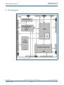
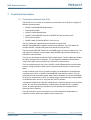
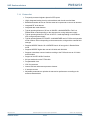
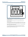
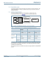
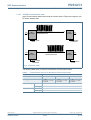
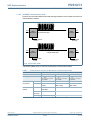
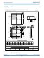
PN532/C1 Near Field Communication (NFC) controller Rev. 3.0 — 10 November 2011 120130 Product short data sheet COMPANY PUBLIC 1. General description The PN532 is a highly integrated transceiver module for contactless communication at 13.56 MHz based on the 80C51 microcontroller core. It supports 6 different operating modes: • • • • ISO/IEC 14443A/MIFARE Reader/Writer FeliCa Reader/Writer ISO/IEC 14443B Reader/Writer ISO/IEC 14443A/MIFARE Card MIFARE Classic 1K or MIFARE Classic 4K card emulation mode • FeliCa Card emulation • ISO/IEC 18092, ECMA 340 Peer-to-Peer The PN532 implements a demodulator and decoder for signals from ISO/IEC 14443A/MIFARE compatible cards and transponders. The PN532 handles the complete ISO/IEC 14443A framing and error detection (Parity & CRC). The PN532 supports MIFARE Classic 1K or MIFARE Classic 4K card emulation mode. The PN532 supports contactless communication using MIFARE Higher transfer speeds up to 424 kbit/s in both directions. The PN532 can demodulate and decode FeliCa coded signals. The PN532 handles the FeliCa framing and error detection. The PN532 supports contactless communication using FeliCa Higher transfer speeds up to 424 kbit/s in both directions. The PN532 supports layers 2 and 3 of the ISO/IEC 14443 B Reader/Writer communication scheme, except anticollision. This must be implemented in firmware as well as upper layers. In card emulation mode, the PN532 is able to answer to a Reader/Writer command either according to the FeliCa or ISO/IEC 14443A/MIFARE card interface scheme. The PN532 generates the load modulation signals, either from its transmitter or from the LOADMOD pin driving an external active circuit. A complete secure card functionality is only possible in combination with a secure IC using the NFC-WI/S2C interface. Compliant to ECMA 340 and ISO/IEC 18092 NFCIP-1 Passive and Active communication modes, the PN532 offers the possibility to communicate to another NFCIP-1 compliant device, at transfer speeds up to 424 kbit/s.The PN532 handles the complete NFCIP-1 framing and error detection. The PN532 transceiver can be connected to an external antenna for Reader/Writer or Card/PICC modes, without any additional active component. PN532/C1 NXP Semiconductors Near Field Communication (NFC) controller The PN532 supports the following host interfaces: • SPI • I2C • High Speed UART (HSU) An embedded low-dropout voltage regulator allows the device to be connected directly to a battery. In addition, a power switch is included to supply power to a secure IC. 2. Features and benefits 80C51 microcontroller core with 40 KB ROM and 1 KB RAM Highly integrated demodulator and decoder Buffered output drivers to connect an antenna with minimum number of external components Integrated RF level detector Integrated data mode detector Supports ISO/IEC 14443A/MIFARE Supports ISO/IEC 14443B (Reader/Writer mode only) Typical operating distance in Reader/Writer mode for communication to ISO/IEC 14443A/MIFARE, ISO/IEC 14443B or FeliCa cards up to 50 mm depending on antenna size and tuning Typical operating distance in NFCIP-1 mode up to 50 mm depending on antenna size, tuning and power supply Typical operating distance in ISO/IEC 14443A/MIFARE or FeliCa card emulation mode of approximately 100 mm depending on antenna size, tuning and external field strength Supports MIFARE Classic 1K or MIFARE Classic 4K encryption in Reader/Writer mode and MIFARE higher transfer speed communication at 212 kbit/s and 424 kbit/s Supports contactless communication according to the FeliCa protocol at 212 kbit/s and 424 kbit/s Integrated RF interface for NFCIP-1 up to 424 kbit/s Possibility to communicate on the RF interface above 424 kbit/s using external analog components Supported host interfaces SPI interface I2C interface High-speed UART Dedicated host interrupts Low power modes Hard-Power-Down mode (1 A typical) Soft-Power-Down mode (22A typical) Automatic wake-up on I2C, HSU and SPI interfaces when device is in Power-down mode Programmable timers Crystal oscillator 2.7 to 5.5 V power supply operating range PN512_SDS_120130 Product short data sheet COMPANY PUBLIC All information provided in this document is subject to legal disclaimers. Rev. 3.0 — 10 November 2011 120130 © NXP B.V. 2011. All rights reserved. 2 of 27 PN532/C1 NXP Semiconductors Near Field Communication (NFC) controller Power switch for external secure companion chip Dedicated IO ports for external device control Integrated antenna detector for production tests ECMA 373 NFC-WI interface to connect an external secure IC 3. Applications Mobile and portable devices Consumer applications 4. Quick reference data Table 1. Quick reference data Symbol Parameter PN512_SDS_120130 Product short data sheet COMPANY PUBLIC Conditions VBAT Battery supply voltage ICVDD LDO output voltage VBAT > 3.4 V VSS = 0 V PVDD Supply voltage for host interface SVDD Min Typ Max 2.7 Unit 5.5 V 2.7 3 3.4 V VSS = 0 V 1.6 - 3.6 V Output voltage for secure IC interface VSS = 0 V (SVDD Switch Enabled) DVDD -0.5 - DVDD V IHPD Hard-Power-Down current consumption VBAT = 5 V - - 2 A ISPD Soft-Power-Down current consumption VBAT = 5 V, RF level detector on - - 45 A IDVDD Digital supply current VBAT = 5 V, SVDD switch off - 25 - mA ISVDD SVDD load current VBAT = 5 V, SVDD switch on - - 30 mA IAVDD Analog supply current VBAT = 5 V - 6 - mA - 60[3] 150[4] mA - - 0.5 W -30 - +85 C ITVDD Transmitter supply current During RF transmission, VBAT = 5 V Ptot Continuous total power dissipation Tamb Operating temperature range Tamb = -30 to +85 C [1] [1] [2] [1] DVDD, AVDD and TVDD must always be at the same supply voltage. [2] The total current consumption depends on the firmware version (different internal IC clock speed) [3] With an antenna tuned at 50 at 13.56 MHz [4] The antenna should be tuned not to exceed this current limit (the detuning effect when coupling with another device must be taken into account) All information provided in this document is subject to legal disclaimers. Rev. 3.0 — 10 November 2011 120130 © NXP B.V. 2011. All rights reserved. 3 of 27 PN532/C1 NXP Semiconductors Near Field Communication (NFC) controller 5. Ordering information Table 2. Ordering information Type number Package Name PN512_SDS_120130 Product short data sheet COMPANY PUBLIC Description Version PN5320A3HN/C1xx[1][4] HVQFN40 Heatsink Very thin Quad Flat package; 40 pins, plastic, body 6 x 6 x 0.85 mm; leadless; MSL level 2[3]. SOT618-1 PN5321A3HN/C1xx[1][2][4] HVQFN40 Heatsink Very thin Quad Flat package; 40 pins, plastic, body 6 x 6 x 0.85 mm; leadless; MSL level 2[3]. SOT618-1 [1] xx refers to the ROM code version. The ROM code functionalities are described in the User-Manual document. Each ROM code has its own User-Manual. [2] This NXP IC is licensed under Innovatron’s ISO/IEC 14443 Type B patent license. [3] This is tested according the joint IPC/JEDEC standard J-STD-020C of July 2004. [4] Purchase of an NXP Semiconductors IC that complies with one of the NFC Standards (ISO/IEC18.092; ISO/IEC21.481) does not convey an implied license under any patent right on that standards. A license for the portfolio of the NFC Standards patents of NXP B.V. needs to be obtained at Via Licensing, the pool agent of the NFC Patent Pool, e-mail: [email protected]. All information provided in this document is subject to legal disclaimers. Rev. 3.0 — 10 November 2011 120130 © NXP B.V. 2011. All rights reserved. 4 of 27 PN532/C1 NXP Semiconductors Near Field Communication (NFC) controller 6. Block diagram Fig 1. Block diagram of PN532 PN512_SDS_120130 Product short data sheet COMPANY PUBLIC All information provided in this document is subject to legal disclaimers. Rev. 3.0 — 10 November 2011 120130 © NXP B.V. 2011. All rights reserved. 5 of 27 PN532/C1 NXP Semiconductors Near Field Communication (NFC) controller 7. Functional description 7.1 Contactless Interface Unit (CIU) The PN532 CIU is a modem for contactless communication at 13.56 MHz. It supports 6 different operating modes • • • • • • ISO/IEC 14443A/MIFARE Reader/Writer. FeliCa Reader/Writer. ISO/IEC 14443B Reader/Writer ISO/IEC 14443A/MIFARE Card 1K or MIFARE 4K card emulation mode FeliCa Card emulation ISO/IEC 18092, ECMA 340 NFCIP-1 Peer-to-Peer The CIU implements a demodulator and decoder for signals from ISO/IEC 14443A/MIFARE compatible cards and transponders. The CIU handles the complete ISO/IEC 14443A framing and error detection (Parity & CRC). The CIU supports MIFARE Classic 1K or MIFARE Classic 4K card emulation mode. The CIU supports contactless communication using MIFARE Higher transfer speeds up to 424 kbit/s in both directions. The CIU can demodulate and decode FeliCa coded signals. The CIU digital part handles the FeliCa framing and error detection. The CIU supports contactless communication using FeliCa Higher transfer speeds up to 424 kbit/s in both directions. The CIU supports layers 2 and 3 of the ISO/IEC 14443 B Reader/Writer communication scheme, except anticollision which must be implemented in firmware as well as upper layers. In card emulation mode, the CIU is able to answer to a Reader/Writer command either according to the FeliCa or ISO/IEC 14443A/MIFARE card interface scheme. The CIU generates the load modulation signals, either from its transmitter or from the LOADMOD pin driving an external active circuit. A complete secure card functionality is only possible in combination with a secure IC using the NFC-WI/S2C interface. Compliant to ECMA 340 and ISO/IEC 18092 NFCIP-1 Passive and Active communication modes, the CIU offers the possibility to communicate to another NFCIP-1 compliant device, at transfer speeds up to 424 kbit/s.The CIU handles the complete NFCIP-1 framing and error detection. The CIU transceiver can be connected to an external antenna for Reader/Writer or Card/PICC modes, without any additional active component. PN512_SDS_120130 Product short data sheet COMPANY PUBLIC All information provided in this document is subject to legal disclaimers. Rev. 3.0 — 10 November 2011 120130 © NXP B.V. 2011. All rights reserved. 6 of 27 PN532/C1 NXP Semiconductors Near Field Communication (NFC) controller 7.1.1 Feature list • • • • • • Frequently accessed registers placed in SFR space Highly integrated analog circuitry to demodulate and decode received data Buffered transmitter drivers to minimize external components to connect an antenna. Integrated RF level detector Integrated data mode detector Typical operating distance of 50 mm in ISO/IEC 14443A/MIFARE or FeliCa in Reader/Writer mode depending on the antenna size, tuning and power supply • Typical operating distance of 50 mm in NFCIP-1 mode depending on the antenna size, tuning and power supply • Typical operating distance in ISO/IEC 14443A/MIFARE card or FeliCa card operation mode of about 100 mm depending on the antenna size, tuning and the external field strength • Supports MIFARE Classic 1K or MIFARE Classic 4K encryption in Reader/Writer mode • Supports MIFARE higher data rate at 212 kbit/s and 424 kbit/s • Supports contactless communication according to the FeliCa scheme at 212 kbit/s and 424 kbit/s • • • • • • • PN512_SDS_120130 Product short data sheet COMPANY PUBLIC Support of the NFC-WI/S2C interface 64 byte send and receive FIFO-buffer Programmable timer CRC Co-processor Internal self test and antenna presence detector 2 interrupt sources Adjustable parameters to optimize the transceiver performance according to the antenna characteristics All information provided in this document is subject to legal disclaimers. Rev. 3.0 — 10 November 2011 120130 © NXP B.V. 2011. All rights reserved. 7 of 27 PN532/C1 NXP Semiconductors Near Field Communication (NFC) controller 7.1.2 Simplified block diagram PN532 80C51 Data Mode Detector Serial Data Switch CL UART RF Level Detector Analog Interface Antenna FIFO Contactless Interface Unit Fig 2. Simplify Contactless Interface Unit (CIU) block diagram The Analog Interface handles the modulation and demodulation of the analog signals according to the Card emulation mode, Reader/Writer mode and NFCIP-1 mode communication scheme. The RF level detector detects the presence of an external RF-field delivered by the antenna to the RX pin. The data mode detector detects a ISO/IEC 14443-A MIFARE, FeliCa or NFCIP-1 mode in order to prepare the internal receiver to demodulate signals, which are sent to the PN532. The NFC-WI/S2C interface supports communication to secure IC. It also supports digital signals for transfer speeds above 424 kbit/s. The CL UART handles the protocol requirements for the communication schemes in co-operation with the appropriate firmware. The FIFO buffer allows a convenient data transfer from the 80C51 to the CIU and vice versa. PN512_SDS_120130 Product short data sheet COMPANY PUBLIC All information provided in this document is subject to legal disclaimers. Rev. 3.0 — 10 November 2011 120130 © NXP B.V. 2011. All rights reserved. 8 of 27 PN532/C1 NXP Semiconductors Near Field Communication (NFC) controller 7.1.3 Reader/Writer modes All indicated modulation indices and modes in this chapter are system parameters. This means that beside the IC settings a suitable antenna tuning is required to achieve the optimal performance. 7.1.3.1 ISO/IEC 14443A Reader/Writer The following diagram describes the communication on a physical level, the communication overview in the Table 145 describes the physical parameters. 1. PCD to PICC 100% ASK, Miller Coded, Transfer speed 106 to 424 kbit/s Battery ISO/IEC 14443A Card / PICC PN532 HOST 2. PICC to PCD, Subcarrier Load modulation, Manchester Coded or BPSK, Transfer speed 106 to 424 kbit/s Reader/Writer Fig 3. ISO/IEC 14443A/MIFARE Reader/Writer communication diagram Table 3. Communication overview for ISO/IEC 14443A/MIFARE Reader/Writer Communication scheme ISO/IEC 14443A MIFARE MIFARE Higher Baud Rate Baud rate 106 kbit/s 212 kbit/s Bit length 128 -------------------------- 9,44s 13,56MHz 64 -------------------------- 4,72s 13,56MHz 424 kbit/s 32 -------------------------- 2,36s 13,56MHz PN532 to PICC/Card Modulation 100% ASK 100% ASK 100% ASK Bit coding Modified Miller coding Modified Miller coding Modified Miller coding PICC/Card to PN532 Modulation Subcarrier load modulation Subcarrier load modulation Subcarrier load modulation Subcarrier frequency 13.56 MHz⁄ 13.56 MHz⁄ 13.56 MHz⁄ 16 Bit coding Manchester coding 16 BPSK 16 BPSK The internal CRC co-processor calculates the CRC value according the data coding and framing defined in the ISO/IEC 14443A part 3, and handles parity generation internally according to the transfer speed. With appropriate firmware, the PN532 can handle the complete ISO/IEC 14443A/MIFARE protocol. PN512_SDS_120130 Product short data sheet COMPANY PUBLIC All information provided in this document is subject to legal disclaimers. Rev. 3.0 — 10 November 2011 120130 © NXP B.V. 2011. All rights reserved. 9 of 27 PN532/C1 NXP Semiconductors Near Field Communication (NFC) controller Fig 4. Data coding and framing according to ISO/IEC 14443A PN512_SDS_120130 Product short data sheet COMPANY PUBLIC All information provided in this document is subject to legal disclaimers. Rev. 3.0 — 10 November 2011 120130 © NXP B.V. 2011. All rights reserved. 10 of 27 PN532/C1 NXP Semiconductors Near Field Communication (NFC) controller 7.1.3.2 FeliCa Reader/Writer The following diagram describes the communication at the physical level. Table 146 describes the physical parameters. 1. Reader/Writer to Card 8 - 30% ASK, Manchester Coded, Baud rate 212 to 424 kbit/s Battery FeliCa Card PN532 HOST 2. Card to Reader/Writer, >12% ASK load modulation, Manchester Coded, Baud rate 212 to 424 kbit/s Reader/Writer Fig 5. FeliCa Reader/Writer communication diagram Table 4. Communication overview for FeliCa Reader/Writer Communication scheme FeliCa FeliCa higher baud rate Baud rate 212 kbit/s 424 kbit/s Bit length 64 -------------------------- 4,72s 13,56MHz PN532 to PICC/Card Modulation PICC/Card to PN532 32 -------------------------- 2,36s 13,56MHz 8 - 30% ASK 8 - 30% ASK Bit coding Manchester coding Manchester coding Modulation >12% ASK >12% ASK Bit coding Manchester coding Manchester coding With appropriate firmware, the PN532 can handle the FeliCa protocol. The FeliCa Framing and coding must comply with the following table: Table 5. FeliCa Framing and Coding Preamble 00h 00h SYNC 00h 00h 00h 00h B2h LEN n-Data CRC 4Dh To enable the FeliCa communication a 6-byte preamble (00h, 00h, 00h, 00h, 00h, 00h) and 2-byte SYNC bytes (B2h, 4Dh) are sent to synchronize the receiver. The following LEN byte indicates the length of the sent data bytes plus the LEN byte itself. The CRC calculation is done according to the FeliCa definitions with the MSB first. To transmit data on the RF interface, the 80C51 has to send the LEN and data bytes to the CIU. The Preamble and SYNC bytes are generated by the CIU automatically and must not be written to the FIFO. The CIU performs internally the CRC calculation and adds the result to the frame. The starting value for the CRC Polynomial is 2 null bytes: (00h), (00h) Example of frame: Table 6. FeliCa framing and coding Preamble 00 PN512_SDS_120130 Product short data sheet COMPANY PUBLIC 00 SYNC 00 00 00 00 B2 4D All information provided in this document is subject to legal disclaimers. Rev. 3.0 — 10 November 2011 120130 LEN 2 Data Bytes CRC 03 AB 90 CD 35 © NXP B.V. 2011. All rights reserved. 11 of 27 PN532/C1 NXP Semiconductors Near Field Communication (NFC) controller 7.1.3.3 ISO/IEC 14443B Reader/Writer The CIU supports layers 2 and 3 of the ISO/IEC 14443 B Reader/Writer communication scheme, except anticollision which must be implemented in firmware as well as upper layers. The following diagram describes the communication at the physical level. Table 149 describes the physical parameters. 1. PCD to PICC, 8 - 14% ASK, NRZ-L Coded, Transfer speed 106 to 424 kbit/s Battery ISO/IEC 14443B Card / PICC PN532 HOST 2. PICC to PCD, Subcarrier Load modulation, BPSK, Transfer speed 106 to 424kbit/s Reader/Writer Fig 6. ISO/IEC 14443B Reader/Writer communication diagram With appropriate firmware, the PN532 can handle the ISO/IEC 14443B protocol. Table 7. PN512_SDS_120130 Product short data sheet COMPANY PUBLIC Communication overview for ISO/IEC 14443B Reader/Writer Communication scheme ISO/IEC 14443B Type B higher baud rate Baud rate 106 kbit/s 212 kbit/s Bit length 128 -------------------------- 9,44s 13,56MHz PN532 to PICC/Card Modulation PICC/Card to PN532 64 -------------------------- 4,72s 13,56MHz 424 kbit/s 32 -------------------------- 2,36s 13,56MHz 8 -14% ASK 8 -14% ASK 8 -14% ASK Bit coding NRZ-L NRZ-L NRZ-L Modulation Subcarrier load modulation Subcarrier load modulation Subcarrier load modulation Subcarrier frequency 13.56 MHz⁄ 16 13.56 MHz⁄ 16 13.56 MHz⁄ Bit coding BPSK BPSK BPSK All information provided in this document is subject to legal disclaimers. Rev. 3.0 — 10 November 2011 120130 16 © NXP B.V. 2011. All rights reserved. 12 of 27 PN532/C1 NXP Semiconductors Near Field Communication (NFC) controller 7.1.4 ISO/IEC 18092, ECMA 340 NFCIP-1 operating mode A NFCIP-1 communication takes place between 2 devices: • Initiator: generates RF field at 13.56 MHz and starts the NFCIP-1 communication. • Target: responds to initiator command either in a load modulation scheme in Passive Communication mode or using a self generated and self modulated RF field for Active Communication mode. The NFCIP-1 communication differentiates between Active and Passive communication modes. • Active Communication mode means both the initiator and the target are using their own RF field to transmit data • Passive Communication mode means that the Target answers to an Initiator command in a load modulation scheme. The Initiator is active in terms of generating the RF field. In order to fully support the NFCIP-1 standard the PN532 supports the Active and Passive Communications mode at the transfer speeds 106 kbit/s, 212 kbit/s and 424 kbit/s as defined in the NFCIP-1 standard Battery Battery PN532 PN532 HOST HOST Initiator: Active Target: Passive or Active Fig 7. NFCIP-1 mode With appropriate firmware, the PN532 can handle the NFCIP-1 protocol, for all communication modes and data rates, for both Initiator and Target. PN512_SDS_120130 Product short data sheet COMPANY PUBLIC All information provided in this document is subject to legal disclaimers. Rev. 3.0 — 10 November 2011 120130 © NXP B.V. 2011. All rights reserved. 13 of 27 PN532/C1 NXP Semiconductors Near Field Communication (NFC) controller 7.1.4.1 ACTIVE Communication mode Active Communication Mode means both the Initiator and the Target are using their own RF field to transmit data. Host PN532 NFC Initiator 1. Initiator starts the communication at selected transfer speed PN532 NFC Target Power to generate the field Host Powered for Digital Communication 2. Target answers at the same transfer speed PN532 NFC Initiator Host PN532 NFC Target Powered for Digital Communication Host Power to generate the field Fig 8. Active NFC mode The following table gives an overview of the active communication modes: Table 8. Communication overview for NFC Active Communication mode Communication scheme ISO/IEC 18092, ECMA 340, NFCIP-1 Baud rate 106 kbit/s Bit length 128 -------------------------- 9,44s 13,56MHz Initiator to Target Modulation 100% ASK Bit coding Miller Coded Target to Initiator Modulation 100% ASK Bit coding PN512_SDS_120130 Product short data sheet COMPANY PUBLIC Miller Coded 212 kbit/s 64 -------------------------- 4,72s 13,56MHz 32 -------------------------- 2,36s 13,56MHz 8-30%ASK 8-30%ASK Manchester Coded Manchester Coded 8-30%ASK 8-30%ASK Manchester Coded Manchester Coded All information provided in this document is subject to legal disclaimers. Rev. 3.0 — 10 November 2011 120130 424 kbit/s © NXP B.V. 2011. All rights reserved. 14 of 27 PN532/C1 NXP Semiconductors Near Field Communication (NFC) controller 7.1.4.2 PASSIVE Communication mode Passive Communication Mode means that the target answers to an Initiator command in a load modulation scheme. Host PN532 NFC Initiator 1. Initiator starts communication at selected transfer speed PN532 NFC Target Power for digital processing Power to generate the field Host 2. Targets answers using load modulation at the same transfer speed PN532 NFC Initiator Host Power to generate the field PN532 NFC Target Host Power for digital processing Fig 9. Passive NFC mode The following table gives an overview of the active communication modes: Table 9. PN512_SDS_120130 Product short data sheet COMPANY PUBLIC Communication overview for NFC Passive Communication mode Communication scheme ISO/IEC 18092, ECMA 340, NFCIP-1 Baud rate 106 kbit/s Bit length 128 -------------------------- 9,44s 13,56MHz 212 kbit/s 64 -------------------------- 4,72s 13,56MHz 424 kbit/s 32 -------------------------- 2,36s 13,56MHz PN532 to PICC/Card Modulation 100% ASK 100% ASK 100% ASK Bit coding Modified Miller coding Modified Miller coding PICC/Card to PN532 Modulation Subcarrier load modulation >12% ASK >12% ASK Modified Miller coding Subcarrier frequency 13.56 MHz⁄ 16 No subcarrier No subcarrier Bit coding Manchester coding Manchester coding Manchester coding All information provided in this document is subject to legal disclaimers. Rev. 3.0 — 10 November 2011 120130 © NXP B.V. 2011. All rights reserved. 15 of 27 PN532/C1 NXP Semiconductors Near Field Communication (NFC) controller 7.1.4.3 NFCIP-1 framing and coding The NFCIP-1 framing and coding in Active and Passive communication modes are defined in the NFCIP-1 standard: ISO/IEC 18092 or ECMA 340. 7.1.4.4 NFCIP-1 protocol support The NFCIP-1 protocol is not completely described in this document. For detailed explanation of the protocol refer to the ISO/IEC 18092 / ECMA340 NFCIP-1 standard. However the datalink layer is according to the following policy: • Transaction includes initialization, anticollision methods and data transfer. This sequence must not be interrupted by another transaction. • Speed should not be changed during a data transfer In order not to disturb current infrastructure based on 13.56 MHz general rules to start NFC communication are defined in the following way: • • • • Per default NFCIP-1 device is in target mode, meaning its RF field is switched off. The RF level detector is active. Only if application requires the NFCIP-1 device shall switch to Initiator mode. Initiator shall only switch on its RF field if no external RF field is detected by RF Level detector during a time of TIDT. • The initiator performs initialization according to the selected mode. PN512_SDS_120130 Product short data sheet COMPANY PUBLIC All information provided in this document is subject to legal disclaimers. Rev. 3.0 — 10 November 2011 120130 © NXP B.V. 2011. All rights reserved. 16 of 27 PN532/C1 NXP Semiconductors Near Field Communication (NFC) controller 7.1.5 Card operating modes The PN532 can be addressed like a FeliCa or ISO/IEC 14443A/MIFARE card. This means that the PN532 can generate an answer in a load modulation scheme according to the ISO/IEC 14443A/MIFARE or FeliCa interface description. Remark: The PN532 does not support a secure storage of data. This has to be handled by a dedicated secure IC or a host. The secure IC is optional. Remark: The PN532 can not be powered by the field in this mode and needs a power supply. 7.1.5.1 ISO/IEC 14443A/MIFARE card operating mode With appropriate firmware, the PN532 can handle the ISO/IEC 14443A including the level 4, and the MIFARE protocols. The following diagram describes the communication at the physical level. Table 152 describes the physical parameters. 1. PCD to PICC, 100% ASK, Modified Miller Coded, Transfer speed 106 to 424 kbit/s ISO/IEC 14443A Reader/Writer Battery PN532 HOST 2. PICC to PCD, Subcarrier Load modulation, Manchester Coded or BPSK, Transfer speed 106 to 424kbit/s Card operating mode Fig 10. ISO/IEC 14443A/MIFARE card operating mode communication diagram Table 10. PN512_SDS_120130 Product short data sheet COMPANY PUBLIC Communication overview for ISO/IEC 14443A/MIFARE Card operating mode Communication scheme ISO/IEC 14443A MIFARE MIFARE higher baud rate Baud rate 106 kbit/s 212 kbit/s Bit length 128 -------------------------- 9,44s 13,56MHz 64 -------------------------- 4,72s 13,56MHz 424 kbit/s 32 -------------------------- 2,36s 13,56MHz Reader/Writer to PN532 Modulation 100% ASK 100% ASK 100% ASK Bit coding Modified Miller coding Modified Miller coding Modified Miller coding PN532 to Reader/Writer Modulation Subcarrier load modulation Subcarrier load modulation Subcarrier load modulation Subcarrier frequency 13.56 MHz⁄ 16 13.56 MHz⁄ 16 13.56 MHz⁄ 16 Bit coding Manchester coding BPSK BPSK All information provided in this document is subject to legal disclaimers. Rev. 3.0 — 10 November 2011 120130 © NXP B.V. 2011. All rights reserved. 17 of 27 PN532/C1 NXP Semiconductors Near Field Communication (NFC) controller 7.1.5.2 FeliCa Card operating mode With appropriate firmware, the PN532 can handle the FeliCa protocol. The following diagram describes the communication at the physical level. Table 153 describes the physical parameters. 1. Reader/Writer to Card 8 - 30% ASK, Manchester Coded, Baud rate 212 to 424 kbit/s FeliCa Reader/Writer Battery PN532 HOST 2. Card to Reader/Writer, >12% ASK load modulation, Manchester Coded, Baud rate 212 to 424 kbit/s Card operating mode Fig 11. FeliCa card operating mode communication diagram Table 11. Communication overview for FeliCa Card operating mode Communication scheme FeliCa FeliCa higher baud rate Baud rate 212 kbit/s 424 kbit/s Bit length 64 -------------------------- 4,72s 13,56MHz 32 -------------------------- 2,36s 13,56MHz Reader/Writer to PN532 Modulation 8 - 30% ASK 8 - 30% ASK Bit coding Manchester coding Manchester coding PN532 to Reader/Writer Modulation >12% ASK >12% ASK Bit coding Manchester coding Manchester coding 7.1.6 Overall CIU block diagram The PN532 supports different contactless communication modes. The CIU supports the internal 80C51 for the different selected communication schemes such as Card Operation mode, Reader/Writer Operating mode or NFCIP-1 mode up to 424 kbit/s. The CIU generates bit- and byte-oriented framing and handles error detection according to these different contactless protocols. Higher transfer speeds up to 3.39 Mbit/s can be handled by the digital part of the CIU. To modulate and demodulate the data an external circuit has to be connected to the communication interface pins SIGIN/SIGOUT. Remark: The size and tuning of the antenna have an important impact on the achievable operating distance. PN512_SDS_120130 Product short data sheet COMPANY PUBLIC All information provided in this document is subject to legal disclaimers. Rev. 3.0 — 10 November 2011 120130 © NXP B.V. 2011. All rights reserved. 18 of 27 PN532/C1 NXP Semiconductors Near Field Communication (NFC) controller PN532 80C51 CIU State Machine CIU_Command register Control Register bank Programmable timer CIU FIFO control CIU FIFO control CIU interrupt control CIU 64-byte FIFO CRC16 generation & check MIFARE Classic unit Parallel/Serial Converter Random Number Generator Bit Counter Antenna presence Self Test Parity Generation & Check Frame Generation & Check Bit Bit decoding decoding Card Mode Detector Clock generation Filtering Distribution Amplitude Amplitude Rating rating LOADMOD SIGIN Serial Data Switch Analog-to-Digital Converter Reference Voltage VMID Bit coding Temperature sensor RF clock recovery I-channel Amplifier(LNA) Q-channel Amplifier(LNA) I-channel Demodulator Q-channel Demodulator RF level Detector RX SIGOUT Transmitter control TX1 driver TX2 driver TX1 TX2 Fig 12. CIU detailed block diagram PN512_SDS_120130 Product short data sheet COMPANY PUBLIC All information provided in this document is subject to legal disclaimers. Rev. 3.0 — 10 November 2011 120130 © NXP B.V. 2011. All rights reserved. 19 of 27 PN532/C1 NXP Semiconductors Near Field Communication (NFC) controller 8. Limiting values Table 12. Limiting values In accordance with the Absolute Maximum Rating System (IEC 60134). Symbol Parameter Product short data sheet COMPANY PUBLIC Min Max Unit PVDD Supply Voltage -0.5 4 V VBAT Power Supply Voltage -0.5 6.0 V Ptot Total power dissipation - 500 mW - 150 mA - 30 mA [1] ITVDD Maximum current in TVDD ISVDD Maximum current in SVDD switch VESD Electrostatic discharge voltage VESDH ESD Susceptibility (Human Body model) 1500 , 100pF; EIA/JESD22-A114-D - 2.0 kV VESDM ESD Susceptibility (Machine model) 0.75 mH, 200 pF; EIA/JESD22-A115-A - 200 VESDC ESD Susceptibility (Charge Device Field induced model; model) EIA/JESC22-C101-C - 1.0 kV Tstg Storage temperature -55 150 C Tj Junction temperature -40 125 C [1] PN512_SDS_120130 Conditions V The antenna should be tuned not to exceed this current limit (the detuning effect when coupling with another device must be taken into account) All information provided in this document is subject to legal disclaimers. Rev. 3.0 — 10 November 2011 120130 © NXP B.V. 2011. All rights reserved. 20 of 27 PN532/C1 NXP Semiconductors Near Field Communication (NFC) controller 9. Application information Battery SVDD PMU Secure SIGOUT VBAT Core SIGIN DVDD 4.7uF P34 / SIC_CLK X7R or X5R PN532 100nF CRx 1nF 100nF RX AVDD R1 1 k 100nF R2 2.7 k VMID 4.7uF X7R Cvmid 100nF TVDD 100nF 560nH or L0 X5R C1 RQ TX1 100nF 220pF PVDD TVSS1 TVSS2 RTSPD_N Host - Processor C1 and C2 are matching cap (10 to 300pF) Rq is the damping resistor (several ohms) C0 C2 C0 C2 Antenna 220pF Host Interface TX2 L0 P70_IRQ 560nH C1 RQ Optional LOADMOD TESTEN AVSS DVSS OSCIN 22pF OSCOUT 27.12 MHz R3 1 k R4 1 k 22 pF Fig 13. Application diagram of PN532 In the example the 27.12MHz quartz is a TAS-3225A, SMD PN512_SDS_120130 Product short data sheet COMPANY PUBLIC All information provided in this document is subject to legal disclaimers. Rev. 3.0 — 10 November 2011 120130 © NXP B.V. 2011. All rights reserved. 21 of 27 PN532/C1 NXP Semiconductors Near Field Communication (NFC) controller 10. Package outline HVQFN40: plastic thermal enhanced very thin quad flat package; no leads; 40 terminals; body 6 x 6 x 0.85 mm A B D SOT618-1 terminal 1 index area A E A1 c detail X C e1 e 1/2 e 20 y y1 C v M C A B w M C b 11 L 21 10 e e2 Eh 1/2 1 e 30 terminal 1 index area 40 31 Dh X 0 2.5 DIMENSIONS (mm are the original dimensions) UNIT mm A(1) max. A1 b 1 0.05 0.00 0.30 0.18 5 mm scale c D(1) Dh E(1) Eh 0.2 6.1 5.9 4.25 3.95 6.1 5.9 4.25 3.95 e e1 4.5 0.5 e2 L v w y y1 4.5 0.5 0.3 0.1 0.05 0.05 0.1 Note 1. Plastic or metal protrusions of 0.075 mm maximum per side are not included. REFERENCES OUTLINE VERSION IEC JEDEC JEITA SOT618-1 --- MO-220 --- EUROPEAN PROJECTION ISSUE DATE 01-08-08 02-10-22 Fig 14. Package outline HVQFN40 (SOT618-1) This package is MSL level 2. PN512_SDS_120130 Product short data sheet COMPANY PUBLIC All information provided in this document is subject to legal disclaimers. Rev. 3.0 — 10 November 2011 120130 © NXP B.V. 2011. All rights reserved. 22 of 27 PN532/C1 NXP Semiconductors Near Field Communication (NFC) controller 11. Abbreviations Table 13. PN512_SDS_120130 Product short data sheet COMPANY PUBLIC Abbreviations Acronym Description ASK Amplitude Shift keying BPSK Bit Phase Shift Keying CRC Cyclic Redundancy Check ECMA European Computer Manufacturers Association organization HPD Hard Power Down HSU High Speed UART Initiator Generates RF field at 13.56 MHz and starts the NFCIP-1 communication. LDO Low Drop-Out regulator MSL Moisture Sensitivity Level NFCIP NFC Interface and Protocol NFC-WI NFC Wired Interface to connect NFC front end to a SIC PCD Proximity Coupling Device. Definition for a Card Reader/ Writer according to the ISO/IEC 14443 Specification PICC Proximity Cards. Definition for a contactless Smart Card according to the ISO/IEC 14443 specification SIC Secure Integrated Circuit (can be a Smart Card IC, a Secure Access Module (SAM),...) SPI Serial Parallel Interface SPD Soft Power Down mode Target Responds to initiator command either using load modulation scheme (RF field generated by Initiator) or using modulation of self-generated RF field (no RF field generated by initiator during target answer). UART Universal Asynchronous Receive Transmit All information provided in this document is subject to legal disclaimers. Rev. 3.0 — 10 November 2011 120130 © NXP B.V. 2011. All rights reserved. 23 of 27 PN532/C1 NXP Semiconductors Near Field Communication (NFC) controller 12. Revision history Table 14. Revision history Document ID Release date Data sheet status Change notice Supersedes PN532_SDS_120130 20111110 Product short data sheet - 120112 Modifications: 120112 PN512_SDS_120130 Product short data sheet COMPANY PUBLIC • The format of this data sheet has been redesigned to comply with the new identity guidelines of NXP Semiconductors. • • Legal texts have been adapted to the new company name where appropriate. General update 20060112 Short form data sheet - All information provided in this document is subject to legal disclaimers. Rev. 3.0 — 10 November 2011 120130 - © NXP B.V. 2011. All rights reserved. 24 of 27 PN532/C1 NXP Semiconductors Near Field Communication (NFC) controller 13. Legal information 13.1 Data sheet status Document status[1][2] Product status[3] Definition Objective [short] data sheet Development This document contains data from the objective specification for product development. Preliminary [short] data sheet Qualification This document contains data from the preliminary specification. Product [short] data sheet Production This document contains the product specification. [1] Please consult the most recently issued document before initiating or completing a design. [2] The term ‘short data sheet’ is explained in section “Definitions”. [3] The product status of device(s) described in this document may have changed since this document was published and may differ in case of multiple devices. The latest product status information is available on the Internet at URL http://www.nxp.com. 13.2 Definitions Draft — The document is a draft version only. The content is still under internal review and subject to formal approval, which may result in modifications or additions. NXP Semiconductors does not give any representations or warranties as to the accuracy or completeness of information included herein and shall have no liability for the consequences of use of such information. Short data sheet — A short data sheet is an extract from a full data sheet with the same product type number(s) and title. A short data sheet is intended for quick reference only and should not be relied upon to contain detailed and full information. For detailed and full information see the relevant full data sheet, which is available on request via the local NXP Semiconductors sales office. In case of any inconsistency or conflict with the short data sheet, the full data sheet shall prevail. Product specification — The information and data provided in a Product data sheet shall define the specification of the product as agreed between NXP Semiconductors and its customer, unless NXP Semiconductors and customer have explicitly agreed otherwise in writing. In no event however, shall an agreement be valid in which the NXP Semiconductors product is deemed to offer functions and qualities beyond those described in the Product data sheet. 13.3 Disclaimers Limited warranty and liability — Information in this document is believed to be accurate and reliable. However, NXP Semiconductors does not give any representations or warranties, expressed or implied, as to the accuracy or completeness of such information and shall have no liability for the consequences of use of such information. In no event shall NXP Semiconductors be liable for any indirect, incidental, punitive, special or consequential damages (including - without limitation - lost profits, lost savings, business interruption, costs related to the removal or replacement of any products or rework charges) whether or not such damages are based on tort (including negligence), warranty, breach of contract or any other legal theory. Notwithstanding any damages that customer might incur for any reason whatsoever, NXP Semiconductors’ aggregate and cumulative liability towards customer for the products described herein shall be limited in accordance with the Terms and conditions of commercial sale of NXP Semiconductors. Right to make changes — NXP Semiconductors reserves the right to make changes to information published in this document, including without limitation specifications and product descriptions, at any time and without notice. This document supersedes and replaces all information supplied prior to the publication hereof. Suitability for use — NXP Semiconductors products are not designed, authorized or warranted to be suitable for use in life support, life-critical or safety-critical systems or equipment, nor in applications where failure or PN512_SDS_120130 Product short data sheet COMPANY PUBLIC malfunction of an NXP Semiconductors product can reasonably be expected to result in personal injury, death or severe property or environmental damage. NXP Semiconductors accepts no liability for inclusion and/or use of NXP Semiconductors products in such equipment or applications and therefore such inclusion and/or use is at the customer’s own risk. Applications — Applications that are described herein for any of these products are for illustrative purposes only. NXP Semiconductors makes no representation or warranty that such applications will be suitable for the specified use without further testing or modification. Customers are responsible for the design and operation of their applications and products using NXP Semiconductors products, and NXP Semiconductors accepts no liability for any assistance with applications or customer product design. It is customer’s sole responsibility to determine whether the NXP Semiconductors product is suitable and fit for the customer’s applications and products planned, as well as for the planned application and use of customer’s third party customer(s). Customers should provide appropriate design and operating safeguards to minimize the risks associated with their applications and products. NXP Semiconductors does not accept any liability related to any default, damage, costs or problem which is based on any weakness or default in the customer’s applications or products, or the application or use by customer’s third party customer(s). Customer is responsible for doing all necessary testing for the customer’s applications and products using NXP Semiconductors products in order to avoid a default of the applications and the products or of the application or use by customer’s third party customer(s). NXP does not accept any liability in this respect. Limiting values — Stress above one or more limiting values (as defined in the Absolute Maximum Ratings System of IEC 60134) will cause permanent damage to the device. Limiting values are stress ratings only and (proper) operation of the device at these or any other conditions above those given in the Recommended operating conditions section (if present) or the Characteristics sections of this document is not warranted. Constant or repeated exposure to limiting values will permanently and irreversibly affect the quality and reliability of the device. Terms and conditions of commercial sale — NXP Semiconductors products are sold subject to the general terms and conditions of commercial sale, as published at http://www.nxp.com/profile/terms, unless otherwise agreed in a valid written individual agreement. In case an individual agreement is concluded only the terms and conditions of the respective agreement shall apply. NXP Semiconductors hereby expressly objects to applying the customer’s general terms and conditions with regard to the purchase of NXP Semiconductors products by customer. No offer to sell or license — Nothing in this document may be interpreted or construed as an offer to sell products that is open for acceptance or the grant, conveyance or implication of any license under any copyrights, patents or other industrial or intellectual property rights. Export control — This document as well as the item(s) described herein may be subject to export control regulations. Export might require a prior authorization from competent authorities. All information provided in this document is subject to legal disclaimers. Rev. 3.0 — 10 November 2011 120130 © NXP B.V. 2011. All rights reserved. 25 of 27 PN532/C1 NXP Semiconductors Near Field Communication (NFC) controller Quick reference data — The Quick reference data is an extract of the product data given in the Limiting values and Characteristics sections of this document, and as such is not complete, exhaustive or legally binding. Non-automotive qualified products — Unless this data sheet expressly states that this specific NXP Semiconductors product is automotive qualified, the product is not suitable for automotive use. It is neither qualified nor tested in accordance with automotive testing or application requirements. NXP Semiconductors accepts no liability for inclusion and/or use of non-automotive qualified products in automotive equipment or applications. In the event that customer uses the product for design-in and use in automotive applications to automotive specifications and standards, customer (a) shall use the product without NXP Semiconductors’ warranty of the product for such automotive applications, use and specifications, and (b) whenever customer uses the product for automotive applications beyond NXP Semiconductors’ specifications such use shall be solely at customer’s own risk, and (c) customer fully indemnifies NXP Semiconductors for any liability, damages or failed product claims resulting from customer design and use of the product for automotive applications beyond NXP Semiconductors’ standard warranty and NXP Semiconductors’ product specifications. 13.4 Licenses Purchase of NXP ICs with NFC technology Purchase of an NXP Semiconductors IC that complies with one of the Near Field Communication (NFC) standards ISO/IEC 18092 and ISO/IEC 21481 does not convey an implied license under any patent right infringed by implementation of any of those standards. A license for the patents portfolio of NXP B.V. for the NFC standards needs to be obtained at Via Licensing, the pool agent of the NFC Patent Pool, e-mail: [email protected]. Purchase of NXP ICs with ISO/IEC 14443 type B functionality This NXP Semiconductors IC is ISO/IEC 14443 Type B software enabled and is licensed under Innovatron’s Contactless Card patents license for ISO/IEC 14443 B. The license includes the right to use the IC in systems and/or end-user equipment. RATP/Innovatron Technology 13.5 Trademarks Notice: All referenced brands, product names, service names and trademarks are the property of their respective owners. I2C-bus — logo is a trademark of NXP B.V. MIFARE — is a trademark of NXP B.V. 14. Contact information For more information, please visit: http://www.nxp.com For sales office addresses, please send an email to: [email protected] PN512_SDS_120130 Product short data sheet COMPANY PUBLIC All information provided in this document is subject to legal disclaimers. Rev. 3.0 — 10 November 2011 120130 © NXP B.V. 2011. All rights reserved. 26 of 27 PN532/C1 NXP Semiconductors Near Field Communication (NFC) controller 15. Contents 1 2 3 4 5 6 7 7.1 7.1.1 7.1.2 7.1.3 7.1.3.1 7.1.3.2 7.1.3.3 7.1.4 7.1.4.1 7.1.4.2 7.1.4.3 7.1.4.4 7.1.5 7.1.5.1 7.1.5.2 7.1.6 8 9 10 11 12 13 13.1 13.2 13.3 13.4 13.5 14 15 General description . . . . . . . . . . . . . . . . . . . . . . 1 Features and benefits . . . . . . . . . . . . . . . . . . . . 2 Applications . . . . . . . . . . . . . . . . . . . . . . . . . . . . 3 Quick reference data . . . . . . . . . . . . . . . . . . . . . 3 Ordering information . . . . . . . . . . . . . . . . . . . . . 4 Block diagram . . . . . . . . . . . . . . . . . . . . . . . . . . 5 Functional description . . . . . . . . . . . . . . . . . . . 6 Contactless Interface Unit (CIU) . . . . . . . . . . . . 6 Feature list . . . . . . . . . . . . . . . . . . . . . . . . . . . . 7 Simplified block diagram. . . . . . . . . . . . . . . . . . 8 Reader/Writer modes . . . . . . . . . . . . . . . . . . . . 9 ISO/IEC 14443A Reader/Writer . . . . . . . . . . . . 9 FeliCa Reader/Writer . . . . . . . . . . . . . . . . . . . 11 ISO/IEC 14443B Reader/Writer . . . . . . . . . . . 12 ISO/IEC 18092, ECMA 340 NFCIP-1 operating mode. . . . . . . . . . . . . . . . . . . . . . . . 13 ACTIVE Communication mode. . . . . . . . . . . . 14 PASSIVE Communication mode . . . . . . . . . . 15 NFCIP-1 framing and coding . . . . . . . . . . . . . 16 NFCIP-1 protocol support . . . . . . . . . . . . . . . . 16 Card operating modes . . . . . . . . . . . . . . . . . . 17 ISO/IEC 14443A/MIFARE card operating mode. . . . . . . . . . . . . . . . . . . . . . . . 17 FeliCa Card operating mode. . . . . . . . . . . . . . 18 Overall CIU block diagram . . . . . . . . . . . . . . . 18 Limiting values. . . . . . . . . . . . . . . . . . . . . . . . . 20 Application information. . . . . . . . . . . . . . . . . . 21 Package outline . . . . . . . . . . . . . . . . . . . . . . . . 22 Abbreviations . . . . . . . . . . . . . . . . . . . . . . . . . . 23 Revision history . . . . . . . . . . . . . . . . . . . . . . . . 24 Legal information. . . . . . . . . . . . . . . . . . . . . . . 25 Data sheet status . . . . . . . . . . . . . . . . . . . . . . 25 Definitions . . . . . . . . . . . . . . . . . . . . . . . . . . . . 25 Disclaimers . . . . . . . . . . . . . . . . . . . . . . . . . . . 25 Licenses . . . . . . . . . . . . . . . . . . . . . . . . . . . . . 26 Trademarks. . . . . . . . . . . . . . . . . . . . . . . . . . . 26 Contact information. . . . . . . . . . . . . . . . . . . . . 26 Contents . . . . . . . . . . . . . . . . . . . . . . . . . . . . . . 27 Please be aware that important notices concerning this document and the product(s) described herein, have been included in section ‘Legal information’. © NXP B.V. 2011. All rights reserved. For more information, please visit: http://www.nxp.com For sales office addresses, please send an email to: [email protected] Date of release: 10 November 2011 120130