1
ELE800 Design Project Report
Enhancing a 68HC11 Processor Board
Shawn D’Alimonte 951-652-742
Department of Electrical and Computer Engineering
Ryerson Polytechnic University
Faculty Supervisor: Prof. P. D. Hiscocks
March 2000
Abstract
This report details some improvements made to the 68HC11 based MPP processor board used in several classes at Ryerson Polytechnic University.
Since the students assembling the board may not have access to device programmers, the EPROM and GAL were replaced with easier-to-program parts.
An EEPROM was substituted for the EPROM and an in-system programmable
GAL was used to replace the MPP board’s GAL. These devices can be quickly
and easily programmed from a PC with only simple cables.
The LCD panel interface was also changed to remain within rated specifications even when the 68HC11 was run at 2MHz or 3MHz. This was accomplished
by generating the LCD panel control signals and data lines from an output port.
Since software determined the timing of the signals, proper operation could be
guaranteed at any clock speed simply by changing the software.
The monitor was also updated to make it easier to use. When an unhandled
interrupt occurs the monitor now displays a suitable error message and the
register contents as an aid to debugging.
To allow the user to test the operation and configuration of the RAM a
routine to test and count the memory was added to the monitor.
ii
Acknowledgements
Thanks to my faculty advisor Prof. P. D. Hiscocks for providing help and
suggestions with this project.
iii
Contents
1 Introduction
2
2 Objectives
3
3 Replacing the MPP Board EPROM with EEPROM
3.1 EEPROM Theory . . . . . . . . . . . . . . . . . . . . . . .
3.1.1 EEPROM Description . . . . . . . . . . . . . . . . .
3.2 EEPROM Bootstrapping . . . . . . . . . . . . . . . . . . .
3.3 EEPROM Design Issues . . . . . . . . . . . . . . . . . . . .
3.4 EEPROM Hardware Design . . . . . . . . . . . . . . . . . .
3.5 EEPROM Software Design . . . . . . . . . . . . . . . . . .
3.5.1 68HC11 Bootstrap Portion of the EEPROM Loader
3.5.2 PC Portion of 68HC11 EEPROM Loader . . . . . .
3.6 EEPROM Operation Overview . . . . . . . . . . . . . . . .
3.7 Challenges in Implementing EEPROM . . . . . . . . . . . .
3.8 Performance of EEPROM . . . . . . . . . . . . . . . . . . .
.
.
.
.
.
.
.
.
.
.
.
.
.
.
.
.
.
.
.
.
.
.
.
.
.
.
.
.
.
.
.
.
.
4
4
4
5
7
7
10
10
12
13
13
13
4 Replacing the Address Decoder GAL with an In-system Programmable Device
4.1 Theory of the ISP GAL . . . . . . . . . . . . . . . . . . . . . . .
4.2 ISP GAL Design Issues . . . . . . . . . . . . . . . . . . . . . . .
4.3 ISP GAL Hardware Design . . . . . . . . . . . . . . . . . . . . .
4.3.1 ispGAL Socket Adapter for MPP Board Address Decoder
4.3.2 ispGAL Programming Cable . . . . . . . . . . . . . . . .
4.3.3 GAL Address Decoder Design Equations . . . . . . . . . .
4.4 ISP GAL Software Design . . . . . . . . . . . . . . . . . . . . . .
4.5 Challenges in implementing ISP GAL . . . . . . . . . . . . . . .
4.6 Performance of ISP GAL . . . . . . . . . . . . . . . . . . . . . .
15
15
16
16
16
16
18
18
18
19
5 LCD Interface Changes to Allow Higher E-Clock
5.1 LCD Module Interface Theory . . . . . . . . . . .
5.2 LCD Module Interface Design Issues . . . . . . . .
5.3 LCD Module Interface Hardware Design . . . . . .
5.4 LCD Module Interface Software Design . . . . . .
20
20
22
22
23
iv
Rates
. . . .
. . . .
. . . .
. . . .
.
.
.
.
.
.
.
.
.
.
.
.
.
.
.
.
5.5
5.6
5.4.1 LCD Panel Initialization for 4 bit Operation
5.4.2 Timing for the LCD Display Interface . . . .
5.4.3 LCD Module Interface Operation Overview .
Challenges in implementing LCD Module Interface .
Performance of LCD Module Interface . . . . . . . .
.
.
.
.
.
.
.
.
.
.
.
.
.
.
.
.
.
.
.
.
.
.
.
.
.
.
.
.
.
.
.
.
.
.
.
6 Improvements to the Buffalo Monitor used on the 68HC11 Processor Module
6.1 Memory Counting and Testing . . . . . . . . . . . . . . . . . . .
6.1.1 Memory Counting Design Issues . . . . . . . . . . . . . .
6.1.2 Memory Counting and Testing Software Design . . . . . .
6.1.3 Memory Counter and Tester Operation Overview . . . . .
6.1.4 Challenges in implementing the Memory Count and Test
6.1.5 Performance of Memory Count and Test Routines . . . .
6.2 Improving the Buffalo Monitor Handling of Unhandled Interrupts
6.2.1 Unhandled Interrupt Handler Design Issues . . . . . . . .
6.2.2 Unhandled Interrupt Handler Software Design . . . . . .
6.2.3 Interrupt Handler Operation Overview . . . . . . . . . . .
6.2.4 Challenges in implementing the Unhandled Interrupt Handler . . . . . . . . . . . . . . . . . . . . . . . . . . . . . .
6.2.5 Performance of the Unhandled Interrupt Handler . . . . .
6.3 New LCD Driver Routines for Buffalo Monitor . . . . . . . . . .
6.4 Other Improvements Made to the Buffalo Monitor . . . . . . . .
6.4.1 Removing Excess I/O Code from the Buffalo Monitor . .
6.4.2 Adding More Functions to the Jump Table . . . . . . . .
7 Conclusions
24
24
24
25
25
26
27
27
27
27
28
28
29
29
29
30
30
30
30
30
30
31
32
8 Recommendations for Implementing Improvements
33
8.1 Recommendations for Use of EEPROM on the MPP Board . . . 33
8.2 Recommendations for Implementing the ISP GAL on the MPP
Board . . . . . . . . . . . . . . . . . . . . . . . . . . . . . . . . . 33
8.3 Recommendations for Updated LCD Display Interface on MPP
Board . . . . . . . . . . . . . . . . . . . . . . . . . . . . . . . . . 34
8.4 Recommendations for Monitor Updates for MPP Board . . . . . 35
References
37
A Bootstrapping the 68HC11 Processor Board
39
A.1 Programming the ispGAL . . . . . . . . . . . . . . . . . . . . . . 39
A.2 Programming the EEPROM . . . . . . . . . . . . . . . . . . . . . 39
B Buffalo Monitor Subroutine Descriptions and Addresses
v
41
C Description of the 68HC11 Operating Modes
C.1 Single-Chip Mode . . . . . . . . . . . . . . . . .
C.2 Expanded Mode . . . . . . . . . . . . . . . . .
C.3 Bootstrap Mode . . . . . . . . . . . . . . . . .
C.4 Special Test Mode . . . . . . . . . . . . . . . .
.
.
.
.
.
.
.
.
.
.
.
.
.
.
.
.
.
.
.
.
.
.
.
.
.
.
.
.
.
.
.
.
.
.
.
.
.
.
.
.
42
42
42
43
43
D LCD Module Information
44
D.1 LCD Module Command List . . . . . . . . . . . . . . . . . . . . 44
D.2 LCD Module Initialization for 4-bit Mode Operation . . . . . . . 45
E ABEL Source Code for MPP Board Address Decoder GAL
46
E.1 ABEL Source Code . . . . . . . . . . . . . . . . . . . . . . . . . . 46
E.2 ABEL Test Vectors for MPP Address Decoder GAL . . . . . . . 48
E.3 ispEXPERT Compiler Report for MPP Address Decoder GAL . 50
F LCD Module Interface
F.1 LCDINIT . . . . . .
F.2 LCDDAT . . . . . .
F.3 LCDCTL . . . . . .
F.4 WCTRL . . . . . . .
F.5 WDAT . . . . . . . .
F.6 Delay Routines . . .
Software
. . . . . .
. . . . . .
. . . . . .
. . . . . .
. . . . . .
. . . . . .
G EEPROM Loader Software for
G.1 PC Portion of Loader . . . .
G.1.1 eeload.c . . . . . . . .
G.1.2 serial.c . . . . . . . . .
G.1.3 serial.h . . . . . . . .
G.2 68HC11 Bootstrap Loader . .
for MPP
. . . . . .
. . . . . .
. . . . . .
. . . . . .
. . . . . .
. . . . . .
MPP
. . . .
. . . .
. . . .
. . . .
. . . .
Board
. . . . .
. . . . .
. . . . .
. . . . .
. . . . .
. . . . .
Board
. . . . .
. . . . .
. . . . .
. . . . .
. . . . .
.
.
.
.
.
.
.
.
.
.
.
.
.
.
.
.
.
.
.
.
.
.
.
.
.
.
.
.
.
.
.
.
.
.
.
.
.
.
.
.
.
.
.
.
.
.
.
.
.
.
.
.
.
.
.
.
.
.
.
.
.
.
.
55
55
57
57
58
59
59
.
.
.
.
.
.
.
.
.
.
.
.
.
.
.
.
.
.
.
.
.
.
.
.
.
.
.
.
.
.
.
.
.
.
.
.
.
.
.
.
61
61
61
66
69
71
H Source Code for Routines Added to the MPP Board Buffalo
Monitor
76
H.1 Memory Counting and Testing Routine . . . . . . . . . . . . . . 76
H.2 Modified Unhandled Interrupt Handler . . . . . . . . . . . . . . . 79
I
Parts Lists
I.1 EEPROM Adapter Parts List
I.2 ispGAL Adapter Parts List .
I.3 LCD Interface Parts List . . .
I.4 Suppliers . . . . . . . . . . .
.
.
.
.
.
.
.
.
.
.
.
.
.
.
.
.
.
.
.
.
.
.
.
.
.
.
.
.
.
.
.
.
83
83
83
83
84
J Schematics
J.1 Schematic for the EEPROM Socket Adapter . . . .
J.2 Schematic for the ispGAL Socket Adapter . . . . . .
J.2.1 ispGAL Socket Adapter . . . . . . . . . . . .
J.2.2 Schematic of the ispGAL Programming Cable
J.3 LCD Interface Schematics . . . . . . . . . . . . . . .
.
.
.
.
.
.
.
.
.
.
.
.
.
.
.
.
.
.
.
.
.
.
.
.
.
.
.
.
.
.
.
.
.
.
.
85
85
86
86
87
88
.
.
.
.
vi
.
.
.
.
.
.
.
.
.
.
.
.
.
.
.
.
.
.
.
.
.
.
.
.
.
.
.
.
.
.
.
.
.
.
.
.
.
.
.
.
.
.
.
.
List of Figures
3.1
3.2
3.3
3.4
3.5
Timing Diagram of EEPROM Read Cycle . . . . . . . . . . . .
Timing Diagram of EEPROM Write Cycle . . . . . . . . . . . .
Timing Diagram of EEPROM Data Polling . . . . . . . . . . .
Photographs of the EEPROM Socket Adapter . . . . . . . . . .
Pseudocode for 68HC11 Bootstrap Portion of EEPROM Loader
.
.
.
.
.
5
6
6
9
11
4.1
4.2
Photograph of the ispGAL Socket Adapter . . . . . . . . . . . .
Photograph of Author’s Lattice ISP Programming Cable . . . . .
17
17
5.1
5.2
Timing Diagram for Sharp LCD Module Interface . . . . . . . .
Photographs of the LCD Interface Board . . . . . . . . . . . . . .
22
23
6.1
6.2
Algorithm to Determine MPP Board RAM Size . . . . . . . . . .
Step-by-step Operation of the RAM Counting Algorithm . . . . .
27
28
8.1
Recommendations for EPROM/EEPROM Configuration Jumpers for MPP Board . . . . . . . . . . . . . . . . . . . . . . . . . .
34
vii
List of Tables
3.1
3.2
3.3
3.4
EPROM and EEPROM pinouts . . . . . . . . . . . . . . . . . . .
8
Memory Access Time Requirements for 68HC11 . . . . . . . . . .
9
EEPROM Loader PC program command line options . . . . . . 12
EEPROM Loading and Verification Time Using BootStrap Loader 14
4.1
MPP Board Memory Map and Chip Selects . . . . . . . . . . . .
18
5.1
5.2
LCD Module Interface Signal Descriptions . . . . . . . . . . . . .
LCD Module Interface Timing Requirements . . . . . . . . . . .
21
21
6.1
68HC11 Stack Contents After an Interrupt has Occurred . . . . .
29
C.1 68HC11 Operating Modes . . . . . . . . . . . . . . . . . . . . . .
42
viii
Authorship
I, Shawn D’Alimonte, certify that this report is my own work. All work done
by others has been properly referenced.
1
Chapter 1
Introduction
Currently many students assemble the 68HC11 MPP processor board (See [7]
and [12]) for use in several courses at Ryerson. This involves soldering the components in place and then using a device programmer to configure the address
decoder GAL and EPROM.
The current design is very flexible, but has a few drawbacks. The EPROM
and GAL require a device programmer to configure, which requires the student
to come into the lab or purchase an expensive programmer. Also any changes
to the EPROM contents require a rather long erase time under a UV light.
The current LCD panel interface is only rated for a 1MHz clock. Although
many people have reported it working at 2MHz or higher it would be better to
properly support higher clocks.
The monitor’s handling of unexpected interrupts was poor. When something
unexpected happened the monitor simply locked up the system. A proper error
message would be much more helpful to the user.
The user also has no way to know if the RAM is correctly installed, configured
and functional. A simple RAM test would verify the amount and operation of
the memory.
2
Chapter 2
Objectives
The objective of the project was to make the 68HC11 MPP board easier to
construct and use. Specifically, the following improvements were made:
• Use of an in-system programmable replacement for the address decoder
GAL.
• Replaced the EPROM with an EEPROM that could be programmed insystem and easily changed or updated.
• Provided a method to program and verify the address decoder GAL and
EEPROM.
• Allowed more flexibility for the clock rate by changing the LCD interface.
• Added the ability to detect the amount of RAM installed and to test it.
• Handle unexpected interrupts by displaying an error message and restarting.
3
Chapter 3
Replacing the MPP Board
EPROM with EEPROM
Currently the MPP board uses an EPROM to hold the monitor program and
any subroutine libraries that the user needs. This works fine, except that a
programmer is required to store the programs in the EPROM and it can only be
erased by exposure to strong UV light for several minutes. The need for special
equipment, along with the long erase time make the EPROM inconvenient for
many people.
To solve this problem the EPROM can be replaced by another type of nonvolatile memory that can be programmed in-system. In this case the monitor
and libraries can be loaded from a PC over the serial port. This allows anyone
to assemble the board with minimal equipment and to quickly make changes
and updates to the ROM contents. This could also allow user programs to be
stored in EEPROM so they do not have to be reloaded after a power loss.
3.1
3.1.1
EEPROM Theory
EEPROM Description
In this project a 28C64 or 28C256 EEPROM was substituted for the EPROM
to provide 8k or 32k of ROM respectively. The EEPROM has a simple programming algorithm compared to other memory technologies such as FLASH.
The EEPROM allows single bytes to be written and no separate erase cycle is
needed. On the other hand, a FLASH memory must be erased and programmed
in blocks.
EEPROM Operations
The control signals used by the EEPROM are very similar to those of an
SRAM. The control signals are Chip Enable(CE), Output Enable(OE) and
4
Address
CE
OE
WE
Data Out
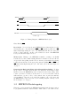
Source: [3]
Figure 3.1: Timing Diagram of EEPROM Read Cycle
Write Enable(W E).
Read Cycle To read a byte from the EEPROM the address is placed on the
address pins (A0 to A14 ) and then the CE and OE signals are pulled low. W E
must remain high during the cycle. The EEPROM will drive the data pins
(I/O0 to I/O7 ) with the contents of the addressed location. The EEPROM
read cycle is shown in figure 3.1 above.
Write Cycle Writing to the EEPROM is similar to writing to an SRAM
but takes about 5ms to finish. During this time no further accesses are allowed
except for the data polling described below. A write cycle is initiated by placing
a valid address and data on the appropriate pins and pulling CE and W E low.
OE must remain high during the cycle. The write cycle is shown in figure 3.2
on page 6.
Detecting the End of the Write Cycle Through Data Polling To allow
the processor to determine when the write cycle has ended, and it is safe to make
further accesses, the EEPROM provides a feature known as data polling. After
a write cycle has been started, as shown above, a read of the same address
will return the opposite of bit 7 of the written data on pin I/O7 until the
cycle is finished. Once the cycle ends I/O7 returns to the correct state and
the EEPROM is ready for the next access. A timing diagram of this process is
shown in figure 3.3 on page 6.
3.2
EEPROM Bootstrapping
When the board is assembled the EEPROM is initially blank. It must somehow
be programmed with the desired software. This could be done with a device
5
Address
CE
OE
WE
Data In
Write Cycle Time
5ms
Source: [3]
Figure 3.2: Timing Diagram of EEPROM Write Cycle
Address
CE
OE
WE
I/O 7
D
7
D
7
D
7
D
7
Write Cycle Starts
D
7
D
7
Write Finished
Data Polling
Source: [3]
Figure 3.3: Timing Diagram of EEPROM Data Polling
6
programmer, but that would defeat the purpose of using EEPROM in the first
place. The 68HC11 provides a bootstrap mode that allows a small program to
be loaded over the serial port. This program can be sent by a PC and used to
program the EEPROM. This allows the 68HC11 to bootstrap itself. For more
information about the 68HC11 bootstrap mode see sections 2.2.3 and 2.2.4 of
the 68HC11 Technical Reference Manual[15] or appendix C on page 42 of this
report.
3.3
EEPROM Design Issues
This portion of the project required determining how to interface an EEPROM
to the 68HC11’s external expansion bus and how to program it from a PC
without any special hardware. The similarity of the control signals to those
of an SRAM or EPROM simplified this. A simple adapter to match the pinouts of the EEPROM to the EPROM socket was needed, but other than that
the EEPROM hardware was straightforward. See section 3.4 for a detailed
description of the adapter.
To load the EEPROM, software was needed for both the PC doing the loading and for the 68HC11 to run during the load. The software for the 68HC11
is sent from the PC using the 68HC11 bootstrap mode. An example of such a
program is given in Motorola Application Note AN1010[2]. This software was
sufficient to load the EEPROM from bootstrap mode while needing no additional hardware. However, the PC program given was written in GWBASIC. Not
having a copy of GWBASIC, or even the more modern QBASIC, the author
was forced to rewrite the PC portion of the program in C. See section 3.5 on
page 10 for more information about the EEPROM loading software.
3.4
EEPROM Hardware Design
The EEPROM has a very similar interface to the EPROM, but some of the pins
are located in different locations. The pin-outs of 8k and 32k EPROMs and
EEPROMs are compared in table 3.1 on page 8. These differences mean that
a socket adapter had to be constructed to fit the EEPROM into the EPROM
socket. The adapter consisted of a small circuit board with the EEPROM socket
attached to it. A wire-wrap socket was placed on the board to form a connector
that fit into the MPP board’s EPROM socket. The schematic for the socket
adapter is in shown in section J.1, page 85. A photograph of the board is shown
in figure 3.4 on page 9. Since the EPROM socket does not provide a write
enable signal it was necessary to connect a wire from the adapter board to the
W E signal on the MPP board expansion connector. A jumper must also be
provided to allow setting the 68HC11 to bootstrap mode. See appendix C or
the 68HC11 manual[15] for details of bootstrap mode.
The only other hardware needed for the EEPROM to function properly was
a small change to the address decoder. According to section 2.2.2 on page
7
Pin No.
1
2
3
4
5
6
7
8
9
10
11
12
13
14
15
16
17
18
19
20
21
22
23
24
25
26
27
28
EPROM
EEPROM
27C256 27C64 28C256 28C64
Vpp
Vpp
A14
RDY /BSY
A12
A12
A12
A12
A7
A7
A7
A7
A6
A6
A6
A6
A5
A5
A5
A5
A4
A4
A4
A4
A3
A3
A3
A3
A2
A2
A2
A2
A1
A1
A1
A1
A0
A0
A0
A0
D0
D0
D0
D0
D1
D1
D1
D1
D2
D2
D2
D2
Vss
Vss
Vss
Vss
D3
D3
D3
D3
D4
D4
D4
D4
D5
D5
D5
D5
D6
D6
D6
D6
D7
D7
D7
D7
CE
CE
CE
CE
A10
A10
A10
A10
OE
OE
OE
OE
A11
A11
A11
A11
A9
A9
A9
A9
A8
A8
A8
A8
A13
NC
A13
NC
A14
P
WE
WE
Vcc
Vcc
Vcc
Vcc
Sources: [14], [13], [1], [3]
Table 3.1: EPROM and EEPROM pinouts
8
U1
J1
J2
J1
R1
R1
Figure 3.4: Photographs of the EEPROM Socket Adapter
E Clock
1MHz
2MHz
3MHz
68HC11 Min. Memory Max.
Access Time
Access Time
442ns
427ns
192ns
177ns
111ns
96ns
Source: [15]
Table 3.2: Memory Access Time Requirements for 68HC11
2-6 of the 68HC11 technical Reference[15] during accesses to internal address
space the 68HC11 still generates address and bus control signals. Since a 32k
EEPROM will overlap the addresses of the internal EEPROM any accesses to
the internal EEPROM will also activate the external EEPROM. When a write
to the 68HC11 internal EEPROM occurred then the external EEPROM would
also enter its write cycle. This would crash the system if the program was
running in EEPROM (Such as the monitor) since the processor will be unable
to fetch the next instruction once the write cycle has started. Also the write
would corrupt the EEPROM. Therefore it was necessary to exclude the internal
EEPROM address range from the external EEPROM chip select range. This
problem did not exist in the EPROM based system since writes to the EPROM
have no effect. A jumper was also provided to disconnect the W E signal when
the EEPROM was not being updated to prevent other unintentional corruption.
The speed of the EEPROM needed depends on the clock speed of the 68HC11
and the speed of the address decoder GAL. The limiting factor is the memory
access time. A summary of the requirements for 1, 2 and 3MHz E clocks is
shown in table 3.2 above. The memory access times determined above assume a
15ns delay from the address decoder GAL. They should be adjusted if a different
speed GAL is used.
9
3.5
EEPROM Software Design
The software to load the EEPROM consists of two parts. One runs on the PC
and sends the second part to the 68HC11 running in bootstrap mode. The first
part, running on the PC, then tells the second part, running on the 68HC11
what action it is to perform. The action can be one of:
• Program 68HC11 Internal EEPROM
• Program External EEPROM or RAM
• Verify Memory
The PC then sends the S19 file containing the program to be loaded or verified.
The 68HC11 echos each received character so that communications errors can be
detected. No other error checking is done. If problems are suspected the loader,
or another program (such as PCBUG11) should be used to verify the memory
contents. Details of the two parts of the loader are given below. Listings of the
software can be found in appendix G and on the enclosed disk.
3.5.1
68HC11 Bootstrap Portion of the EEPROM Loader
This is the program sent to the 68HC11 by the PC. It was published by Motorola
in Application Note AN1010[2], and was used with only minimal modifications.
The bootstrap program first enables the external bus. Then it waits for a
character to indicate the mode. If it receives an ‘X’, ‘I’ or ‘V’ it sets the flags
to indicate the mode. ‘X’ is for programming external EEPROM or RAM, ‘I’
is for programming internal EEPROM and ‘V’ is for verifying either one. The
program then waits for the S19 file to be sent.
For program modes the correct programming algorithm is performed depending on the memory type indicated by the mode flags. For external EEPROM the
data polling method described in section 3.1.1 on page 5 is used. For internal
EEPROM the programming algorithm described in section 3.5.1 of the 68HC11
manual[15] is used.
If verify mode is selected then no writing occurs. Instead the received bytes
are compared to the current memory contents. If they are different then the byte
from memory is sent back to the PC. When finished (as indicated by receiving
an S9 record from the PC) the loader just goes into an endless loop of returning
received characters.
The original version would stop echoing characters when it was done. This
often confused the PC part of the program when there were some blank lines at
the end of the S19 file. The Motorola assembler leaves a blank line at the end
of the S19 files it generates so it was necessary to correct this problem.
The pseudocode for the program described above is presented in figure 3.5
on page 11.
10
1. Wait for character from SCI
X? - Set External EEPROM mode
I? - Set Internal EEPROM mode
V? - Set Verify Mode
other? - Goto 1
2. Wait for character from SCI
not S? - Goto 2
3. Wait for character from SCI
1? - S Record received
- call 4
9? - End of S19 file
- Echo received characters forever
other - Goto 3
4. Get length of record and start address
5. for each byte in record
Get two characters
convert to binary
mode == I? Program to internal EEPROM
mode == X? Program to external EEPROM
Data poll until done
mode == V? Compare received byte to memory
If different send byte in memory back to PC
Skip over checksum
return
Figure 3.5: Pseudocode for 68HC11 Bootstrap Portion of EEPROM Loader
11
Flag
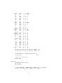
-i
-e
-v
-l loaderfile
-c n
-f n
Last Argument
Description
Load 68HC11 internal EEPROM
Load external EEPROM
Verify memory
bootstrap loader file
Select COM port (1-4)
68HC11 E Clock NOT IMPLEMENTED!
S19 filename
Default
-e
-e
-e
-l EEPROGIX.B00
-c 1
-f 2000000
none
Table 3.3: EEPROM Loader PC program command line options
3.5.2
PC Portion of 68HC11 EEPROM Loader
The PC portion of the loader is responsible for sending the bootloader portion
to the 68HC11. It then sends a single character to indicate the mode and
sends the S19 file containing the program to be loaded or verified. Since all
of the characters sent to the 68HC11 are echoed it is possible to check for
communication errors. A timeout on the receiver is also implemented as an
error check. If no character is received within 5 seconds the program reports
an error and terminates. In verify mode the program waits 10ms after each
character is sent to see if a byte is returned. If so it is displayed to alert the
user to the error. In any mode the characters of the S19 file that are echoed
back are displayed on the screen.
The program was loosely based on the one in AN1010[2], but was rewritten
in C. This was done to improve the performance and readability of the code
and to allow the program to run without a BASIC interpreter present. The
C version of the program was developed using the free DJGPP compiler and
development tools available from [4]. DJGPP is a port of the GNU gcc compiler
to the MS-DOS environment. The EEPROM loader runs under DOS, including
a Windows 98 DOS window and the Linux DOS emulator. Under Windows
the program does not seem to release the serial port until the window is closed.
This means that other programs cannot use the port until the DOS window is
closed. The reason for this behavior is unknown.
The program should be fairly portable to other operating systems. The
only non-portable code should be in serial.c where the serial port is accessed.
These routines could be replaced with the appropriate ones for whatever OS
was needed.
To shorten development time, but still have a useful program, it was developed as a simple DOS command line tool. It understands the command line
arguments shown in table 3.3.
The bootloader program that is sent to the 68HC11 is stored as a straight
binary file. Tools are available on the Internet (See references [8] and [18]) to
convert the S19 output of the assembler into straight binary. This file must be
at least 256 bytes long and the code and data must fit in the first 256 bytes. This
12
is a restriction of the 68HC11 bootstrap mode. The listing of the bootloader
can be found in appendix G on page 61.
3.6
EEPROM Operation Overview
To load the monitor program into the EEPROM the user installs the bootstrap
mode jumpers, to set the MODA and MODB signals low, and resets the 68HC11.
This puts it into bootstrap mode. Then the user ensures the serial cable is
connected between the MPP board and the PC. The program can now be run.
The bootload program is run to load the program into the EEPROM. When it is
finished the program can be run again in verify mode to ensure the programming
was successful. The 68HC11 must be reset between runs of the program. If
multiple non-overlapping S19 files need to be loaded they can be sent one at a
time, remembering to reset the processor between runs. After all the files are
programmed, and optionally verified, the bootstrap jumpers can be removed
and the 68HC11 again reset to begin normal operation.
Appendix A on page 39 contains detailed instructions for using the loader.
3.7
Challenges in Implementing EEPROM
It took much work to determine why writing to the 68HC11 internal EEPROM
was crashing the system and corrupting the monitor. It was not obvious that the
68HC11 would show write cycles on the external bus during internal accesses.
Once that was determined and the address decoder corrected there were no
further problems.
The DOS part of the loader took the most time on this portion of the project.
Most of the work was in figuring out exactly what the 68HC11 portion of the
loader was expecting. The main problem was the poor commenting and structure of the code in the application note.
3.8
Performance of EEPROM
The performance of the loader is based on many factors including reliability, ease
of use and speed. No reliability problems have been noticed with the loader
in many uses. The author doesn’t even bother verifying the loaded program
anymore. The program is easy to use, but the argument parsing is a little weird
if the defaults are not suitable. However there would be very little reason to
change any of the default settings except possibly for the serial port used. The
time it takes the loader to run in various situations is shown in table 3.4 on page
14. The loader speed is good compared to the whole erase-program cycle of a
standard EPROM. Verify performance is so poor as to make the feature next
to useless. Verifying the monitor took a little less than 20 minutes. PCBUG11
or a similar program would make more sense for verifying memory contents.
13
Action OS
Time (mm:ss)
Load
Win98
0:53
Load
Linux/DosEmu/DRDOS
3:20
Verify
Win98
18:08
All time were measured using the Buffalo monitor S19 file. It is 19436 bytes
long. The 68HC11 was running at a 2MHz E clock (8MHz crystal). The PC
was a 366MHz AMD K6-2 with 32MB of RAM running Microsoft Windows 98
or Mandrake Linux 6.0 with DOSEmu 1.0 and Caldera DRDOS 7.02.
Table 3.4: EEPROM Loading and Verification Time Using BootStrap Loader
14
Chapter 4
Replacing the Address
Decoder GAL with an
In-system Programmable
Device
On the current MPP board the address decoding was done by a GAL16V8.
This worked well, but required a programmer to program the device. Many
companies are now making in-system programmable (ISP) logic devices which
are much more convenient. They can be programmed using a simple 4 or 5 wire
serial connection from a PC or microcontroller. This makes programming much
easier.
In this project the Lattice ispGAL22V10C was selected for its small size
and similarity to the GAL16V8 previously used. The ispGAL22V10 comes in
a 28 pin PLCC package and has the same pin-out as a normal GAL22V10.
Programming is done using pins that are not used on the standard 22V10.
4.1
Theory of the ISP GAL
The ispGAL has the same architecture as a normal 22V10 GAL. Each output
can be registered or combinatorial, inverted or not. Switches connect the inputs
and feedbacks to AND arrays that are ORed before going to the output blocks.
See the datasheet[11] for a detailed description of the architecture.
Each switch and control bit in the GAL is referred to as a fuse. Each fuse
is assigned an address and can be set or reset during programming. The design
software creates a JEDEC file that tells the device programmer the state of all of
the fuses. For the ispGAL the device programmer software converts the JEDEC
file to a serial bitstream and sends it to the ispGAL. This is usually done over
a parallel port cable from a PC, but it can also be done from a microcontroller.
15
The JEDEC file can be created with any PAL or GAL design system, such
as PALASM, that supports 22V10 devices. Lattice provides a package called
ispEXPERT which includes schematic and ABEL design entry as well as a
simulator.
4.2
ISP GAL Design Issues
The GAL provides an address decoder. The inputs are the upper 8 bits of the
address bus (A8 to A15 ), the E clock and RW . It generates the R and W read
and write strobes and the chip selects shown in table 4.1 on page 18.
The ispGAL had to function equivalently to the original GAL, but be programmable with minimal hardware. Programming had to be a reasonably simple
and quick procedure.
4.3
4.3.1
ISP GAL Hardware Design
ispGAL Socket Adapter for MPP Board Address
Decoder
The ispGAL is only available in a PLCC28 or SSOP28 package. Since an SSOP
package would be difficult for a student who may not be experienced at soldering
to assemble, the PLCC28 version was chosen. The original GAL16V8 was a DIP
packaged device. Therefore the GAL was mounted on an adapter board which
also provided the connector for the programming cable. The construction of the
adapter was similar to the EEPROM adapter discussed in section 3.4 on page
7. The pinout of the programming connector on the adapter is compatible with
the Lattice ispDOWNLOAD cable described in reference [10]. A photograph of
the adapter is shown in figure 4.1 on page 17. The schematic of the adapter is
shown in section J.2 on page 86.
4.3.2
ispGAL Programming Cable
The ispGAL is usually programmed using a cable from the parallel port of a
PC. Lattice sells the ispDOWNLOAD cable which will program any Lattice
ISP device (See the cable datasheet[10] for more details). Schematics for the
cable were not included in the datasheet so details had to be found elsewhere.
After some searching on the Internet some examples of do-it-yourself cables were
found at references [16] and [17].
Both of these designs were too complicated for the needs of this project.
They have additional logic to support JTAG or 3.3V devices and provide buffering for long cables or programming multiple devices. It turns out that for a short
cable no buffering was required. The cable used is shown in the photograph in
figure 4.2. The schematic is shown in section J.2 on page 86. This cable is only
suitable for the ispGAL device as others need JTAG or the ispEN signal. The
cable must be kept short since no buffering is used.
16
J2
C2
U1
C1
C3
J1
Figure 4.1: Photograph of the ispGAL Socket Adapter
Figure 4.2: Photograph of Author’s Lattice ISP Programming Cable
17
Address Range
$0000-$00FF
$1000-$103F
$1100-$11FF
$1400-$14FF
$1500-$15FF
$1800-$7FFF
$B600-$B7FF
$8000-$FFFF
Chip Select
none
none
IN, OUT
LCD
SEL0
RAM
none
EPROM
Description
68HC11 Internal RAM
68HC11 Internal Registers
Input and Output Ports
LCD Output Port (Write Only)
Spare Chip Select
External RAM
68HC11 Internal EEPROM
External (E)EPROM (Do not activate for $B600-$B7FF)
Table 4.1: MPP Board Memory Map and Chip Selects
4.3.3
GAL Address Decoder Design Equations
The design of the address decoder was largely based on the design of the original
MPP board GAL. The decoder generates the various chip select signals for the
(E)EPROM, RAM, IO Ports and LCD. It also generates a spare chip select
along with read and write strobes. The memory map was not changed, but the
logic was changed slightly for the EEPROM and the new LCD interface. See
sections 3.4 (page 7) and 5.3 (page 23) for what needed to be changed. The
memory map and details for each chip select are shown in table 4.1 above.
The GAL also generates read and write strobes to simplify interfacing with
various peripherals. The strobes go low when the E clock is high and the RW
signal from the 68HC11 is in the appropriate state.
The implementation of this memory map was done in ABEL. ABEL is similar
to equation based GAL/PAL assemblers, but has many more advanced features.
ABEL also supports test vectors that made simulation easy. When the ABEL
source was simulated the results were automatically checked as well as displayed.
The ABEL equation and test vector files are in appendix E on page 46.
4.4
ISP GAL Software Design
All of the software used in this portion of the project was downloaded from Lattice Semiconductors web page(http://www.latticesemi.com). The ispEXPERT
package was used for the design entry, simulation and compilation. The ispDCD
package was used to download the design into the ispGAL. Only ispDCD is needed to program the GAL with the JEDEC file on the included disk. ispEXPERT
or another GAL development system is needed to generate a JEDEC file if
changes are to be made.
4.5
Challenges in implementing ISP GAL
The main challenge with this part of the project was finding the details of
the programmer cable. Lattice have not published the schematic for their
18
ispDOWNLOAD cable for several years. It took some research using Internet search engines to find some suitable schematics for compatible cables. After
reviewing these it was fairly simple to make a simplified cable for the ispGAL.
4.6
Performance of ISP GAL
The ispGAL performed as well as the original GAL. The part used has a 15ns
propagation delay, which is better than the original GAL’s 25ns.
The ease of reprogramming the ispGAL greatly aided the development of the
EEPROM and LCD interface, as the address decoder logic could be changed
quickly and easily. Programming took only a few seconds.
19
Chapter 5
LCD Interface Changes to
Allow Higher E-Clock Rates
Most projects involving the MPP board involve the LCD display. In the original
design the LCD was connected to the 68HC11’s expansion bus. This worked fine
when the board was run with a 1MHz E-Clock, but at higher clock frequencies
the LCD panel’s timing specifications are no longer met by the 68HC11 bus.
Although several people report the display functioning correctly at clock rates as
high as 4MHz the interface was changed to guarantee the timing specifications
at any clock rate.
5.1
LCD Module Interface Theory
The Sharp LM162 LCD module has a simple interface with flexible interfacing
requirements. The signals are shown in table 5.1 on page 21. The timing requirements for the interface are given in table 5.2 on page 21. These specifications
must be met to guarantee the proper operation of the panel.
The operation of the interface is shown in figure 5.1 on page 22. First RS
and R/W are set to the appropriate values. After the setup time E is set to
high. For a write cycle the data is then placed on the data bus and after another
setup time E is set to low. For a read cycle the data appears on the data bus
following the data delay time after E is raised and stays for the data hold time
after E is lowered.
The interface can operate with either an 8 bit or a 4 bit data bus. In 4 bit
mode the 8 bits of each byte of data or command are sent in two cycle, first the
high order bits, then the low order bits. This reduces the number of interface
signals by four.
Although the interface is bidirectional, it is not necessary to implement reading from the LCD. The module provides a read mode so that the busy flag may
be checked to see if the panel has completed the last command. The datasheet
also lists the maximum time for each operation, so that a delay can be used
20
Pin
1
2
3
4
5
6
11-14
7-10
Pin
Signal
VSS
VCC
VO
RS
Description
Ground
Power (5V)
Contrast Voltage
Register Select
High to select data register
Low to select instruction register
R/W
Read/Write
High to read, Low to write
E
Enable - High to initiate access
DB4 -DB7 High order bits of data bus
Used for 4 bit interface
DB7 is also the busy flag
DB0 -DB3 Low order bits of data bus
Not used in 4 bit interface
numbers are given for MPP LCD connector.
Sources: [5], [7]
Table 5.1: LCD Module Interface Signal Descriptions
Value
Parameter
Min. Max.
Enable Cycle Time
1000
Enable Pulse Width(high)
450
Enable Rise/Fall Time
25
Setup Time (RS, RW-E)
140
Hold Time (RS, RW-E)
10
Write Setup Time (Data)
195
Write Hold Time (Data)
10
Read Data Delay Time
320
Read Data Hold Time
20
Source: [5]
Unit
ns
ns
ns
ns
ns
ns
ns
ns
ns
Table 5.2: LCD Module Interface Timing Requirements
21
RS
R/W
E
Data (Write)
Valid Data
Data (Read)
Valid Data
Data Delay Time
Data
Setup
Time
RS,R/W
Setup Time
Hold Times
Source: [5]
Figure 5.1: Timing Diagram for Sharp LCD Module Interface
instead of the busy flag. The other use for a read cycle is to read back the
contents of the display RAM or the character RAM.
5.2
LCD Module Interface Design Issues
The major goal of this part of the project was to redesign the LCD interface to
operate at higher clock frequencies while still keeping the interface simple. The
minimum cycle time for the LCD module is 1000ns as shown in table 5.2, which
limits the direct bus interface to a 1MHz clock. Also the setup and hold times
are not met for higher frequencies. Therefore a different approach was needed.
The method selected was to replace the previous bus version of the LCD
interface with a general purpose output latch. This would allow the 68HC11 to
generate the control signals in software, ensuring that the timing requirements
of the module can be met.
5.3
LCD Module Interface Hardware Design
To keep the interface as simple as possible a four bit write only interface was
used. This allowed the hardware to be kept very simple, while adding slightly
to the software requirements. The 4 bit mode was used to reduce the pin count
so that a single 8 bit port would suffice. An 8 bit interface would require more
complicated hardware, while in 4 bit mode the 4 data bits and 3 control signals
fit in an 8 bit IO port. After selecting 4 bit mode during initialization the
22
J1
U1
J2
Figure 5.2: Photographs of the LCD Interface Board
processor can send each 8 bit command or data byte by first sending the upper
4 bits and then the lower 4 bits.
Reading back from the LCD panel was not supported since it would greatly
complicate the interface to support the bidirectional data bus. The R/W signal
to the LCD was tied low to prevent it from driving the data bus and causing
contention. The disadvantage of the write only interface is that the busy flag can
no longer be read. Instead a delay must be inserted between operations to the
LCD. The delay time is specified in the datasheet[5] and can be implemented as
a simple software loop. A bidirectional interface would also allow the contents
of the display and character RAM to be read, but this feature would rarely be
used.
The interface consists of a latch identical to the output port of the MPP
board. However it was connected to the LCD chip select of the address decoder. The decoder was modified to only latch the data on a write to the port
since it was a unidirectional interface. The prototype of the interface board
was connected to the LCD connector on the MPP and the LCD module was
connected to the interface board. A photo of the board is shown in figure 5.2
and the schematic is in section J.3 on page 88.
5.4
LCD Module Interface Software Design
Since the LCD module interface was changed to an output latch the LCD driver
in the monitor needed to be changed to generate the control signals with the
correct timing as shown above in figure 5.1 above. Since the interface used
was write only, a software delay loop was used for the delay after each LCD
23
operation. The use of a 4 bit interface meant that for each 8 bit command or
data byte the software had to generate the 2 cycles needed to send the byte.
The WDAT and WCTRL routines in the MPP monitor were replaced with
ones implementing the correct 4 bit protocol. WDAT sends a data byte to the
LCD module, while WCTRL sends a command byte. These are the subroutines
used by user programs to access the LCD. Low level routines were also created to
implement the low level accesses. LCDDAT sends a nybble to the LCD as data.
This is called twice by WDAT to send the full byte. A similar routine, LCDCTL,
was created to send one nybble of a command. Listings of the routines can be
found in appendix F on page 55.
5.4.1
LCD Panel Initialization for 4 bit Operation
The LCDINIT routine properly configures the LCD display for 4 bit operation.
It follows the sequence of operations shown in the datasheet[5] and repeated in
section D.2 on page 45. After finishing this sequence the LCD module is ready
for access.
5.4.2
Timing for the LCD Display Interface
The LCD module takes some time to complete an operation. The maximum
time for each operation is listed in the datasheet[5] and in the command list
in section D.1 on page 44. During this time no further operations can occur.
The LCD also provides a busy flag that is available by reading the command
register. When the flag is set the LCD is busy and the processor must wait
before the next operation.
Since the interface constructed did not support reading from the LCD the
busy flag could not be checked. Therefore, delays were inserted after each
operation. Command operations require at most 1.64ms to complete, while
data writes require at most 40µs to finish. The routines WAIT5ms, WAIT2ms
and WAIT50us were written to provide the correct delay. These routines were
written for a 2MHz E clock, but could easily be rewritten to provide sufficient
delay for any clock speed.
Proper setup and hold time is assured by the amount of time the 68HC11
takes between write to the output port. Since it is impossible to change the
output port state in less than 4 cycles the minimum cycle time would be 1µs
at 4MHz, which is the minimum cycle time. Therefore all setup, hold and cycle
times are guaranteed up to an E clock rate of 4MHz.
5.4.3
LCD Module Interface Operation Overview
When the user wished to send a data character to the LCD they would place
the character in register A and call the WDAT function of the monitor. WDAT
will split the data byte into its 2 nybbles and call LCDDAT to send each nybble
to the display. LCDDATA manipulates the output port to generate the control
24
signals necessary to write the nybble. After writing both nybbles WDAT calls
WAIT50us to wait 50µs for the operation to complete.
Writing a control byte follows the same procedure, except that WCTRL is
called by the user. It uses LCDCTL instead of LCDDAT. Since some commands
take 1.64ms a 2ms delay occurs by calling WAIT2ms after a command.
5.5
Challenges in implementing LCD Module
Interface
The LCD interface requires a somewhat strange initialization sequence to operate in 4 bit mode. An error in the initialization instructions on the datasheet
resulted in some confusion. Once the correct command was used the display
worked properly. As well the timing of the control signals is critical for proper
operation of the interface. Because of this, several attempts were needed before
working initialization and communications routines were developed.
5.6
Performance of LCD Module Interface
The LCD will take longer to access with this interface. It takes twice as many
cycles to send each byte as with the 8 bit interface, not counting the overhead
of separating each byte into the two nybbles. The lack of read capability means
that the system must wait the maximum possible delay after each operation.
This means accessing the display will take longer on the interface as implemented.
This slowdown would be counteracted by the higher clock rates possible.
Although it takes more cycles to perform each LCD access the cycle time is
reduced. Therefore the time required to perform an access was not increased as
much as one would expect.
The interface was fast enough for a continuously updating ADC reading
with a bar graph. This application required many LCD operations to update
the display as well as a fair amount of calculation and the display update rate
was far more than sufficient.
25
Chapter 6
Improvements to the
Buffalo Monitor used on the
68HC11 Processor Module
The monitor is a program running on the processor that allows the user to load
and debug programs. The MPP board uses a modified version of Motorola’s
Buffalo monitor. The features of this monitor are:
• Load S19 files from host PC
• Display and Modify memory and registers
• Set breakpoints
• Single step using the timer and the XIRQ interrupt
• Simple interactive assembler
• Many useful IO routines for the serial port
The changes to the monitor were intended to make it more useful. The
changes made were:
• Added memory count and test routine
• Improved interrupt handling. Unhandled interrupts cause a message to
be displayed
• Added support for the new LCD interface (See sections 5.4 (page 23) and
appendix F)
• Removed support for a second serial port since the MPP board does not
have one and likely never will. This was an attempt to reduce the size
of Buffalo to make room for the other additions while still using an 8k
(E)EPROM.
26
1.
2.
3.
4.
Write $FFFF→$7FFE
Write $55AA→$3FFE
Write $AA55→$5FFE
Read $7FFE
$FFFF? - 32k Installed
$55AA? - 16k Installed
$AA55? - 8k Installed
$Other? - Error
Figure 6.1: Algorithm to Determine MPP Board RAM Size
• Added LCD subroutines to jump table and made sure all useful Buffalo
subroutines were in the jump table.
6.1
6.1.1
Memory Counting and Testing
Memory Counting Design Issues
To determine how much memory was installed a series of writes were made to
various locations in RAM. The partial decoding of the addresses leave ‘mirrors’
of the RAM in the memory map if less than 32k is installed which means that
by picking the order and locations of the writes the amount of memory could
be determined by the result left in one of the addresses.
6.1.2
Memory Counting and Testing Software Design
The algorithm used is shown in figure 6.1. This process relies on the fact that
for an 8k system all three addresses are the same memory location. For a 16k
system $FFFE and $3FFE are the same location, but $5FFE is different. Figure
6.2 on page 28 shows the contents of each of the memory locations after each
step of the process.
After determining how much RAM is present it is tested by writing values to
each location and reading them back. The values used for testing are $00, $55,
$AA and $FF. If an error was detected a message was printed on the terminal
including the address and data of the failure.
The subroutine that performs this operation is included in section H.1 on
page 76.
6.1.3
Memory Counter and Tester Operation Overview
When the user wishes to test the RAM they would type RAMTEST at the
Buffalo prompt. The subroutine would then run and the results were displayed
on the terminal. All of the RAM is cleared by this routine.
27
$FFFF
ROM
8k
$8000
8k
16k
$6000
8k
32k
$4000
8k
16k
Step 1 Step 2
16k
Step 3
Step 1
$7FFE
$FFFF $55AA $AA55 $FFFF
$5FFE
$FFFF $55AA $AA55
$3FFE
$FFFF $55AA $AA55 $FFFF
Step 2
32k
Step 3
Step 1
Step 2
Step 3
$55AA $55AA $FFFF
$FFFF
$FFFF
$AA55
$55AA
$AA55
$55AA $55AA
$2000
$1800
$0000
Figure 6.2: Step-by-step Operation of the RAM Counting Algorithm
6.1.4
Challenges in implementing the Memory Count and
Test
Figuring out the way to detect how much RAM is installed was tricky. The
partial decoding creates mirrors in the memory map so that all of the RAM will
test good, even past the end of real RAM. The solution was to use the differences
in the mirroring between different RAM sizes to determine the amount of RAM
installed.
6.1.5
Performance of Memory Count and Test Routines
The RAM counter was tested with 8k and 32k RAM chips installed and worked
perfectly. Since a 16k RAM chip was not available detecting 16k was tested
by installing the 32k RAM chip with the A14 address line disconnected. In all
cases the amount of installed RAM was properly detected.
To verify that the RAM test worked properly a RAM chip with a data pin
bent up so it was not touching the socket contact was used. The test showed
an appropriate error.
28
Address
Stack Pointer(SP)
SP+1
SP+2
SP+3
SP+4
SP+5
SP+6
SP+7
SP+8
SP+9
Contents
—
CCR
ACCB
ACCA
IXH
IXL
IYH
IYL
PCH
PCL
Table 6.1: 68HC11 Stack Contents After an Interrupt has Occurred
6.2
6.2.1
Improving the Buffalo Monitor Handling of
Unhandled Interrupts
Unhandled Interrupt Handler Design Issues
Before running a user program Buffalo calls the VECINIT subroutine to set
all of the unused interrupt soft vectors to point to a routine called STOPIT.
This causes control to return to the monitor if an unhandled interrupt occurs.
The most common causes of unhandled interrupts are illegal instructions and
enabling interrupts before setting the soft vector. The original STOPIT routine
simply stopped the system by using the STOP instruction in an endless loop.
The goal of the updated routine was to provide a useful response to these
interrupts. In this case a message and the register contents are displayed and
an attempt is made to restart the monitor.
6.2.2
Unhandled Interrupt Handler Software Design
The monitor assumes a soft vector is unused if it does not contain a JMP
instruction to transfer control to the interrupt service routine. Before starting
the user program it sets all unused vectors to point to the STOPIT routine. To
provide a better response the STOPIT routine was replaced by a more advanced
one that displays a message and the register contents. Each soft vector is set
to a different address that prints the correct message for the interrupt received.
The register contents are then displayed by reading them from the stack. The
stack after an interrupt is shown in table 6.1 above. At this point the monitor
attempts to restart the system by jumping to the start of the monitor program.
A listing of the routine is in section H.2 on page 79.
29
6.2.3
Interrupt Handler Operation Overview
When a user program causes an interrupt, but has not set the soft vector to
point to the service routine the STOPIT routine will be called. This will print
the cause of the interrupt and the register contents to help debug the program.
After printing the information Buffalo is restarted.
6.2.4
Challenges in implementing the Unhandled Interrupt Handler
The interrupt handler was fairly straightforward and presented little difficulty
in implementation.
6.2.5
Performance of the Unhandled Interrupt Handler
The interrupt handler was tested with a variety of small programs that generated
various interrupts. The external IRQ and XIRQ pins were also activated. In
each case the correct interrupt was identified and reasonable register contents
were displayed. In each case Buffalo successfully restarted itself without needing
a manual reset.
6.3
New LCD Driver Routines for Buffalo Monitor
These routines were added and modified to support the new LCD interface
described in section 5 on page 20. They are described in detail in section 5.4 on
page 23. The code used is in section F on page 55.
6.4
Other Improvements Made to the Buffalo
Monitor
6.4.1
Removing Excess I/O Code from the Buffalo Monitor
The monitor contained a lot of code detect and use certain kinds of auxiliary
serial ports found on some Motorola evaluation boards. It allowed Buffalo to
use two serial ports: one for the terminal and one for the host. This was
unnecessary for the MPP board which only has one port. The extra code was
just taking up extra ROM space that was put to better use for other features.
Another advantage of this change was the the Buffalo LOAD command no longer
required the T argument. The code was removed to make room for the other
monitor changes while keeping the code under 8k.
30
6.4.2
Adding More Functions to the Jump Table
Users calling Buffalo routines do so through a jump table store at the top of
ROM, just below the vector table. The routines described in the MPP manual
do not cover all of the Buffalo I/O routine, and the LCD routines were missing
altogether. A new jump table is shown in section B on page 41.
31
Chapter 7
Conclusions
The improvements made to the MPP board will make it easier for a student
with limited equipment to program the parts. The ease of programming the
parts also makes the board more flexible. The user can quickly update the
monitor or store programs in the EEPROM. The ease of programming the GAL
makes changing the memory map easier. The unused pins on the GAL could be
used for another purpose simply by reprogramming it. Verifying the EEPROM
contents with the EEPROM loader program is very slow, but programs like
PCBUG11 provide a quick way to verify the memory contents.
The LCD interface update allows the user more flexibility to choose a higher
clock speed for applications that need more processing power without having
to worry about the timing of the LCD panel. The only other change needed to
operate at higher clocks is to change the baud rate of the PC.
The better handling of unexpected interrupts is a big help to debugging. If
the user had forgotten to set the interrupt vector they would receive a useful
error message instead of the system crashing. Since illegal instructions also
generate interrupts, a program that is executing garbage will quickly be stopped
and again a message will be displayed. This would hopefully provide a useful
clue to the problem so it can be quickly located and corrected.
The RAM test functionality added to the monitor is useful to a person who
has just assembled an MPP board and wanted to be sure the RAM was working
properly. The test will verify that the RAM is installed correctly, the chip is
working and the jumpers are set correctly.
These changes will hopefully make the MPP board more useful for the users.
32
Chapter 8
Recommendations for
Implementing
Improvements
8.1
Recommendations for Use of EEPROM on
the MPP Board
For a new version of the MPP board supporting the EEPROM would not require
that much change. The addition of a few jumpers would permit either EPROM
or EEPROM to be used in the same socket. This would make the design very
flexible.
Jumpers would have to be provided to put the 68HC11 into bootstrap mode.
Two jumpers, one from MODA to ground and one from MODB to ground would
suffice for this. The jumpers required to adapt the socket for both EPROMs
and EEPROMs are shown in figure 8.1 on page 34
The loader program is adequate, but some improvements could be made.
The EEPROM supports a block write mode where a group of bytes can be
written during one cycle (See datasheets [1] and [3] for details). This would
speed up the programming, but would need modifications to the loader. Another
useful feature would be to improve the verify mode so that it runs in a reasonable
time.
8.2
Recommendations for Implementing the ISP
GAL on the MPP Board
Switching to the ISP GAL would be fairly simple. A PLCC socket would replace
the current DIP socket and an 8 pin header would be provided for programming.
33
+5V
To (E)EPROM Socket
1
A14
+5V
27
WE
26
Installed Jumper
A13
Possibly Installed Jumper
EPROM
5V
5V
1
5V
1
A14
27
27
WE
5V
A14
5V
A14
A13
1
A14
5V 27
WE
26
27C256
32k
5V
1
27
WE
A13 26
27C128
16k
5V
1
27
WE
A13 26
27C64
8k
5V
1
A14
5V
26
EEPROM Write Protect
EEPROM
5V
WE
A13 26
28C64
8k
A14
27
5V
WE
A13
26
A13
28C256
32k
Figure 8.1: Recommendations for EPROM/EEPROM Configuration Jumpers
for MPP Board
A DOS based GAL loader program would be useful for the Ryerson project
lab which has mostly DOS based PCs. Lattice has some example code, known
as ispCODE[9], that looks like it would be a good start.
If the ispEXPERT software is not available, any PAL or GAL assembler
capable of generating JEDEC files for 22V10 devices can be used. The equations
are shown in the ispEXPERT report file in section E.3 on page 50.
If the ispGAL22V10 is not available a standard GAL22V10 could be substituted since they are pin compatible. However a normal GAL would have to
programmed on a device programmer and then inserted into the socket on the
board. The parallel port programming cable could not be used with a standard
GAL.
8.3
Recommendations for Updated LCD Display Interface on MPP Board
The updated LCD interface guarantees the timing specifications for the LCD
panel by handling the control signals in software. This is adds extra complexity
to the software, but does give the user more flexibility about the clock speed.
If an LCD panel is not needed the interface as presented could be used as 6
general purpose outputs.
34
8.4
Recommendations for Monitor Updates for
MPP Board
The addition of the interrupt handler to the monitor is a big help in debugging
programs, especially if they use interrupts. The error message given is a lot
more helpful than the previous behavior of crashing. The feature would be very
useful.
The RAM test feature, although useful, does take up a lot of ROM space.
Most people are only likely to use it once after assembling the board. It might
be better off as a user program that can be loaded when needed.
35
36
References
[1] 28C64A Datasheet. Microchip, 1998. Doc. No. DS11109J.
http://www.microchip.com/Download/Lit/Memory/Parallel/peeprom/11109j.pdf
[2] AN1010: MC68HC11 EEPROM Programming from a Personal
Computer. Motorola, Inc., 1988. Doc. No AN1010/D.
http://www.mot-sps.com/mcu/documentation/pdf/an1010.pdf
[3] CAT28C256 Datasheet. Catalyst Semiconductor, 1998. Doc. No.
25020-0A 2/98. http://www.catsemi.com/pdf/SPIBus/25C256.pdf
[4] Delorie, DJ. DJGPP Homepage. Internet Website.
http://www.delorie.com/djgpp/
[5] Display Unit User’s Manual. Dot-Matrix LCD Units (With built-in
controllers). Sharp.
http://www.sharpsma.com/datasheets/displays/scm/book1.pdf
[6] HC11: MC68HC11A8 Programming Reference Guide. Motorola, 1990.
Motorola document number MC68HC11A8RG/AD REV. 1
[7] Hiscocks, P. D. 68HC11 Microcontroller Construction and Technical
Manual. Ryerson Polytechnic University.
http://www.ee.ryerson.ca:8080/~jkoch/mppv2/ps files/mpp manual V7.ps
[8] IC Book: HEX/BIN Utility. http://ic.doma.kiev.ua/bios/soft/hex.htm.
[9] ispCODE v.7.1 In-Depth. Lattice Semiconductor, July 1999.
http://www.latticesemi.com/ftp-cgi/nphoasdl.cgi?P AM ID=1152&P CONTACT METHOD=WF
[10] ispDOWNLOAD Cable: Download Cable for In-System Programming of
Lattice ISP Device Families. Lattice Semiconductor, Sept. 1999.
http://www.latticesemi.com/ftp-cgi/nphoasdl.cgi?P AM ID=143&P CONTACT METHOD=W
[11] ispGAL22V10: In-System Programmable E2 CMOS PLD Generic Array
Logic. Lattice Semiconductor Corporation, July 1997.
http://www.latticesemi.com/ftp-cgi/nphoasdl.cgi?P AM ID=100&P CONTACT METHOD=WF
37
[12] Koch, J. The MPP V2 Support Page.
http://www.ee.ryerson.ca:8080/~jkoch/mppv2.htm.
[13] M27C256B Datasheet. ST Microelectronics, 1998.
http://eu.st.com/stonline/books/pdf/docs/2384.pdf
[14] M27C64A Datasheet. ST Microelectronics, March 1998.
http://us.st.com/stonline/books/pdf/docs/2388.pdf
[15] MC68HC11A8 Technical Data. Motorola Inc., 1991. Doc. no.
MC68H11A8/D. http://mot-sps.com/mcu/documentation/pdf/a8.pdf
[16] No Title.
http://www.hszk.bme.hu/~fa218/Download/Lattice download cable.zip
[17] Programmable Logic Devices: Lattice Semiconductor.
http://www.teleport.com/~thandley/Wilbure.htm
[18] Utility Software. SUNSHINE Electronics co. Ltd., Taiwan.
http://danbbs.dk/~rmadrm/utility.htm.
38
Appendix A
Bootstrapping the 68HC11
Processor Board
After assembling the board it will be necessary to first program the GAL and
then the EEPROM. Instructions for doing this are below.
A.1
Programming the ispGAL
1. Connect the programmer cable between the PC’s parallel port and the
programming header on the board.
2. Connect power to the MPP board.
3. Run the ispDCD software.
4. Click on the ‘SCAN’ button on the toolbar.
5. Verify the display shows a single ispGAL22V10.
6. Click on browse and select the JEDEC file to program (Eg. DECODE.JED).
7. Make sure the operation is set to ‘PV’ (Program and Verify)
8. Click the ‘RUN’ gadget.
9. The GAL will now be programmed.
A.2
Programming the EEPROM
1. Ensure an 8MHz crystal is installed on the MPP board (or modify the
baud rate in the DOS software).
2. Connect a serial cable between the MPP boards serial port and the PC.
39
3. Install the MODA and MODB jumpers to select bootstrap mode.
4. Ensure the jumpers are correctly set for the EEPROM. The pin 27 jumper
should be set to WE.
5. Power up or reset the MPP board. The TX LED should now be on.
6. Change the DOS current directory to the location of the bootloader file
(Default EEPROGIX.B00)
7. Type ‘eeload <options> <S19 File>. <options> can be any of the options
show in table 3.3 on page 12.
8. The status will be displayed as the program runs.
9. To write protect the EEPROM move the pin 27 jumper to 5V.
10. Remove the MODA and MODB jumpers and reset the MPP board.
40
Appendix B
Buffalo Monitor Subroutine
Descriptions and Addresses
Routine
LCDPOS
CLRLCD
LCDTEXT
WCTRL
WDAT
WAIT5ms
WAIT2ms
WAIT50us
UPCASE
WCHEK
DCHEK
INPUT
OUTPUT
OUTLHLF
OUTRHLF
OUTA
OUT1BYT
OUT1BSP
OUT2BSP
OUTCRLF
OUTSTRG
OUTSTRG0
INCHAR
Address
$ff64
$ff67
$ff6a
$ff6d
$ff70
$ff73
$ff76
$ff79
$ffa0
$ffa3
$ffa6
$ffac
$ffaf
$ffb2
$ffb5
$ffb8
$ffbb
$ffbe
$ffc1
$ffc4
$ffc7
$ffc7
$ffcd
Description
Set LCD cursor A=Col., B=Line
Clear the LCD display
Print string at X to LCD
Send A to LCD control register
Send A to LCD data register
5ms delay @ E=2Mhz
2ms delay @ E=2MHz
50us delay @ E=2MHz
convert A to upper case
check A for white space (space, tab, comma) Set Z if true
check A for delimiter (WCHEK + EOL) Set Z if true
low level input routine, A=recvd char or 0 if no char
low level output routine. Transmit A
display top 4 bits of A as hex digit
display bottom 4 bits of A as hex digit
output ascii character in A
display the hex value of byte at X
out1byt followed by space
display 2 hex bytes at X and a space
carriage return, line feed to terminal
display string at X (term with $04 or $00)
outstrg with no initial carr ret
wait for and input a char from terminal to A
41
Appendix C
Description of the 68HC11
Operating Modes
The 68HC11 has four operating modes. The mode is selected by the state of
the MODA and MODB pins at reset. Table C.1 shows the various modes and
the MODA and MODB settings that select them.
C.1
Single-Chip Mode
This operating mode is used when the external bus is not required. The pins
used for the bus become parallel ports B and C. Programs are run from internal
EPROM, EEPROM or mask ROM depending on the specific version of the
68HC11.
C.2
Expanded Mode
This is the normal operating mode of the MPP board. The port B and C pins
become external address and data busses. This allows connection to external
Mode
Single-Chip
Expanded
Special Bootstrap
MODA
0
1
0
Special Test
1
MODB
1
1
0
0
Source: [6]
Description
No external bus
External bus enabled
Run program loaded over
serial port
Factory testing mode
Table C.1: 68HC11 Operating Modes
42
memories and peripherals.
C.3
Bootstrap Mode
Bootstrap mode is very useful feature of the 68HC11. It allows the processor
to load a small program over the serial port. This is useful for bootstrapping a
system and for testing. For example, Motorola provides a monitor that runs on
the PC called PCBUG11 that uses bootstrap mode to send a small program to
the 68HC11 that allows the monitor to control the 68HC11.
Bootstrap mode is selected by having the MODA and MODB pins of the
68HC11 low during reset. After resetting in bootstrap mode the 68HC11 sends
a continuous break on the SCI transmitter. The PC then sends the character
$FF. This can occur at 2 baud rates: either E/16 or E/104. This corresponds
to 7812 baud or 1200 baud for a 2MHz E clock. After transmitting the $FF
the PC sends 256 bytes that are stored in the internal RAM of the 68HC11.
Each received character is echoed back to the PC to allow for error checking.
When all 256 bytes are received the 68HC11 jumps to address $0000 to start
the downloaded program.
The external bus is not enabled by default in bootstrap mode. However by
modifying the HPRIO register the program can switch to expanded mode or
special test mode.
C.4
Special Test Mode
This mode is intended for factory testing. It is similar to expanded mode, but
the normal register protection mechanism is disabled to allow testing. Some
additional registers are available, but their function is not useful outside of
testing. This mode has limited use for the user although it could be useful to
allow a monitor to change write-once registers several times.
43
Appendix D
LCD Module Information
D.1
LCD Module Command List
This is the command summary from the LCD module datasheet[5]. For more
details see the datasheet.
Source: [5]
44
D.2
LCD Module Initialization for 4-bit Mode
Operation
The LCD needs to be properly initialized for 4 bit mode. This is the procedure
given in the datasheet[5].
All commands are given in binary and are sent on the upper nybble of the
data bus. When an 8 bit number is shown it is assumed it will be sent over 2
cycles using the 4 bit mode. RS and R/W remain low throughout the process.
1. Wait 15ms from power on
2. Send command nybble 0011
3. Wait 4.1ms
4. Send command nybble 0011
5. Wait 100µs
6. Send command nybble 0011
7. Check Busy Flag or wait 40µs
8. Send command nybble 0010 (Function Set 4bit)
9. Check Busy Flag or wait 40µs
10. Send command byte 00101000 (Function Set)
11. Check Busy Flag or wait 40µs
12. Send command byte 00001000 (Display Off)
13. Check Busy Flag or wait 40µs
14. Send command byte 00000001 (Clear Display)
15. Check Busy Flag or wait 40µs
16. Send command byte 00000110 (Entry Mode Set)
17. Check Busy Flag or wait 40µs
18. Display is now initialized
Source: [5]
Note that there is an error in the initialization sequence shown in the datasheet.
The Function Set command shown is incorrect. Refer to the sequence shown
above or the command summary in the datasheet for the correct command.
45
Appendix E
ABEL Source Code for
MPP Board Address
Decoder GAL
E.1
//
//
//
//
//
//
//
//
//
//
//
//
//
//
//
//
ABEL Source Code
MPP Board Address decoder
Shawn D’Alimonte
Jan 2000
Addresses
EPROM
$8000-$FFFF (Except $B600-$B7FF)
RAM
$1800-$7FFF
IN/OUT $1100-$11FF
LCD
$1400-$14FF
SELECT0 $1500-$15FF
It also generates the /R and /W strobes
This is targeted for the Lattice ispGAL22V10-15J. Other
PLDs should work if you change the pinouts to match and
construct the appropriate socket adapter.
MODULE decode
TITLE ’MPP Board Address Decoder’
Declarations
// Pins
// Pin numbers
46
//sclk
a8
a9
a10
a11
a12
a13
//mode
a14
a15
e
rw
//spare1
//gnd
//sdi
//spare2
//spare3
//spare4
r
w
select0
//sdo
lcd
outp
inp
ram
eprom
//vcc
PIN
PIN
PIN
PIN
PIN
PIN
PIN
PIN
PIN
PIN
PIN
PIN
PIN
PIN
PIN
PIN
PIN
PIN
PIN
PIN
PIN
PIN
PIN
PIN
PIN
PIN
PIN
PIN
1;
2;
3;
4;
5;
6;
7;
8;
9;
10;
11;
12;
13;
14;
15;
16;
17;
18;
19;
20;
21;
22;
23;
24;
25;
26;
27;
28;
//
//
//
//
//
//
//
//
//
//
//
//
//
//
//
//
//
//
//
//
//
//
//
//
//
//
//
//
SCLK
I/CLK
I
I
I
I
I
MODE
I
I
I
I
I
GND
SDI
I
IO
IO
IO
IO
IO
SDO
IO
IO
IO
IO
IO
VCC
a8,a9,a10,a11,a12,a13,a14,a15,rw,e ISTYPE ’com’;
r,w,select0,lcd,outp,inp,ram,eprom ISTYPE ’com’;
// Internal node - hopefully optimized out
//int_eeprom
NODE;
// Alias for address bus
A=[a15..a8];
Equations
// Read and write strobes
!r = rw & e;
!w = !rw & e;
// External EPROM or EEPROM ($8000-$FFFF except int_eeprom)
!eprom = (A >= ^H80) & (A !=^HB6) & (A != ^HB7);
47
// External RAM ($1800-$7FFF)
!ram = (A >= ^H18) & (A <= ^H7F);
// LCD Port ($1400) (Now activates D bus latch on write only)
!lcd = (A == ^H14) & !rw & e;
// IO Port ($1100)
!inp = (A == ^H11) & rw & e;
!outp = (A == ^H11) & !rw & e;
// Spare CS ($1500)
!select0 = (A == ^H15) & e;
END
E.2
ABEL Test Vectors for MPP Address Decoder GAL
// Test vectors for MPP Address decoder
// Shawn D’Alimonte
// Feb 24, 2000
MODULE decode
TITLE ’MPP Board Address Decoder’
Declarations
// Pins
//sclk
a8
a9
a10
a11
a12
a13
//mode
a14
a15
e
rw
//spare1
// Pin numbers
PIN
PIN
PIN
PIN
PIN
PIN
PIN
PIN
PIN
PIN
PIN
PIN
PIN
1;
2;
3;
4;
5;
6;
7;
8;
9;
10;
11;
12;
13;
//
//
//
//
//
//
//
//
//
//
//
//
//
SCLK
I/CLK
I
I
I
I
I
MODE
I
I
I
I
I
48
//gnd
//sdi
//spare2
//spare3
//spare4
r
w
select0
//sdo
lcd
outp
inp
ram
eprom
//vcc
PIN
PIN
PIN
PIN
PIN
PIN
PIN
PIN
PIN
PIN
PIN
PIN
PIN
PIN
PIN
14;
15;
16;
17;
18;
19;
20;
21;
22;
23;
24;
25;
26;
27;
28;
//
//
//
//
//
//
//
//
//
//
//
//
//
//
//
GND
SDI
I
IO
IO
IO
IO
IO
SDO
IO
IO
IO
IO
IO
VCC
a8,a9,a10,a11,a12,a13,a14,a15,rw,e ISTYPE ’com’;
r,w,select0,lcd,outp,inp,ram,eprom ISTYPE ’com’;
// Alias for address bus
A=[a15..a8];
Test_Vectors
( [e, rw, A] -> [r, w, eprom, ram, lcd, inp, outp, select0] )
//
R W EPROM RAM LCD INP OUTP SELECT0
// Read and write strobes
[.C., 1, ^h00] -> [!.C., 1,
1, 1, 1, 1,
1,
[.C., 0, ^h00] -> [1, !.C.,
1, 1, 1, 1,
1,
1];
1];
// External RAM ($1800-$7FFF) reads and
^h18] -> [!.C., 1,
1, 0, 1, 1,
^h18] -> [1, !.C.,
1, 0, 1, 1,
^h7f] -> [!.C., 1,
1, 0, 1, 1,
^h40] -> [!.C., 1,
1, 0, 1, 1,
writes
1,
1,
1,
1,
1];
1];
1];
1];
1,
1,
1,
1];
1];
1];
[.C.,
[.C.,
[.C.,
[.C.,
1,
0,
1,
1,
// External EPROM/EEPROM ($8000-$FFFF)
[.C., 1, ^h80] -> [!.C., 1,
0, 1, 1, 1,
[.C., 1, ^hc0] -> [!.C., 1,
0, 1, 1, 1,
[.C., 1, ^hff] -> [!.C., 1,
0, 1, 1, 1,
// Internal EEPROM ($B600-$B7FF) (EPROM should
// not activate for this case since external EEPROM
// will be corrupted during writes
[.C., 1, ^hb6] -> [!.C., 1,
1, 1, 1, 1,
1,
1];
[.C., 1, ^hb7] -> [!.C., 1,
1, 1, !.C., 1,
1,
1];
49
// LCD Port ($1400)
[.C., 1, ^h14] -> [!.C., 1,
[.C., 0, ^h14] -> [1, !.C.,
1,
1,
1,
1,
1, 1,
1,
.C., 1,
1,
// IO Ports ($1100)
[.C., 1, ^h11] -> [!.C., 1,
[.C., 0, ^h11] -> [1, !.C.,
1,
1,
1,
1,
1,
1,
!.C.,
1,
1,
!.C.,
// Spare ($1500)
[.C., 1, ^h15] -> [!.C., 1,
1,
1,
1,
1,
1,
1];
1];
1];
1];
!.C.];
END
E.3
ispEXPERT Compiler Report for MPP Address Decoder GAL
ispEXPERT 7.1
-
Device Utilization Chart
Page 1
Fri Feb 25 23:31:41 2000
MPP Board Address Decoder
-------------------------------------------------------------------------------Module
: ’decode’
-------------------------------------------------------------------------------Input files:
ABEL PLA file
Device library
: decode.tt3
: P22V10C.dev
Output files:
Report file
: decode.rep
Programmer load file : decode.jed
50
--------------------------------------------------------------------------------
ispEXPERT 7.1
-
Device Utilization Chart
Page 2
Fri Feb 25 23:31:41 2000
MPP Board Address Decoder
P22V10C Programmed Logic:
--------------------------------------------------------------------------------
r
= !(
rw & e );
w
= !(
!rw & e );
select0
lcd
outp
= !(
= !(
= !(
ram
= (
#
#
eprom
!rw & e & !a15 & !a14 & !a13 & a12 & !a11 & a10 & !a9 & !a8 );
= !(
inp
e & !a15 & !a14 & !a13 & a12 & !a11 & a10 & !a9 & a8 );
!rw & e & !a15 & !a14 & !a13 & a12 & !a11 & !a10 & !a9 & a8 );
rw & e & !a15 & !a14 & !a13 & a12 & !a11 & !a10 & !a9 & a8 );
a15
!a14 & !a13 & !a12
!a14 & !a13 & !a11 );
= (
#
ispEXPERT 7.1
!a15
!a14 & a13 & a12 & !a11 & a10 & a9 );
-
Device Utilization Chart
Page 3
Fri Feb 25 23:31:41 2000
MPP Board Address Decoder
P22V10C Chip Diagram:
--------------------------------------------------------------------------------
P22V10C
51
a11
a12
a13
a14
a15
e
e
p
a
r r
1 a a
o a
0 9 8
m m
/---------------------/ 4 3 2 1 28 27 26 |
|
|
| 5
25 |
|
|
| 6
24 |
|
|
| 7
23 |
|
|
| 8
22 |
|
|
| 9
21 |
|
|
| 10
20 |
|
|
| 11
19 |
|
|
| 12 13 14 15 16 17 18 |
-----------------------r
w
!inp
!outp
!lcd
!select0
!w
!r
SIGNATURE: N/A
ispEXPERT 7.1
-
Device Utilization Chart
Page 4
Fri Feb 25 23:31:41 2000
MPP Board Address Decoder
P22V10C Resource Allocations:
--------------------------------------------------------------------------------
Device
| Resource |
Design
|
Resources
| Available | Requirement | Unused
======================|===========|=============|==============
|
|
|
Input Pins:
|
|
|
52
|
|
|
Output Pins:
|
|
In/Out:
|
Output:
|
|
Buried Nodes:
|
|
Input Reg: |
Pin Reg:
|
Buried Reg: |
Input:
ispEXPERT 7.1
-
|
|
|
|
|
|
|
|
|
|
|
|
|
12
10
-
10
-
10
8
-
0
-
Device Utilization Chart
|
|
|
|
|
|
|
|
|
|
|
|
|
2 ( 16 %)
2 ( 20 %)
-
10 (100 %)
-
Page 5
Fri Feb 25 23:31:41 2000
MPP Board Address Decoder
P22V10C Product Terms Distribution:
--------------------------------------------------------------------------------
Signal
|
Pin
| Terms | Terms | Terms
Name
| Assigned | Used | Max | Unused
=========================================|==========|=======|=======|=======
r
|
19
|
1
| 12
| 11
w
|
20
|
1
| 14
| 13
select0
|
21
|
1
| 16
| 15
lcd
|
23
|
1
| 16
| 15
outp
|
24
|
1
| 14
| 13
inp
|
25
|
1
| 12
| 11
ram
|
26
|
3
| 10
|
7
eprom
|
27
|
2
|
8
|
6
==== List of Inputs/Feedbacks ====
Signal Name
| Pin
| Pin Type
=========================================|==========|=========
rw
|
12
| INPUT
e
|
11
| INPUT
a15
|
10
| INPUT
a14
|
9
| INPUT
53
a13
a12
a11
a10
a9
a8
ispEXPERT 7.1
|
|
|
|
|
|
-
Device Utilization Chart
7
6
5
4
3
2
|
|
|
|
|
|
INPUT
INPUT
INPUT
INPUT
INPUT
CLK/IN
Page 6
Fri Feb 25 23:31:41 2000
MPP Board Address Decoder
P22V10C Unused Resources:
--------------------------------------------------------------------------------
Pin
| Pin
|
Product
| Flip-flop
Number | Type |
Terms
|
Type
=======|========|=============|==========
13 | INPUT |
|
16 | INPUT |
|
17 | BIDIR | NORMAL 8
|
D
18 | BIDIR | NORMAL 10
|
D
54
Appendix F
LCD Module Interface
Software for MPP Board
F.1
LCDINIT
*********
* LCDINIT - Initialize LCD display and configure for 4 bit operation
* See pg 14 Fig 4 in datasheet
* Complete the following writes to the command register
* (DB3-DB0 are don’t cares, since they are not connected)
*
* DB7 DB6 DB5 DB4
* 0 0 1 1
Wait 4.1ms
* 0 0 1 1
Wait 100us
* 0 0 1 1
*
* Can now use busy flag
*
* I Function Set
* 0 0 1 0
*
* II Function Set
* 0 0 1 0
* 1 0 0 0
*
* III Display Off
* 0 0 0 0
* 1 0 0 0
*
* IV Display Clear
* 0 0 0 0
* 0 0 0 1
*
* V Entry Mode Set
* 0 0 0 0
* 0 1 1 0
*
55
10
20
30
* At this point we turn on the display
*********
LCDINIT psha
; Init procedure from datasheet
;Wait 15ms
jsr WAIT5ms
jsr WAIT5ms
jsr WAIT5ms
40
ldaa #$03
jsr LCDCTL
jsr WAIT5ms
ldaa #$03
jsr LCDCTL
jsr WAIT5ms
50
ldaa #$03
jsr LCDCTL
jsr WAIT5ms
; Step I
ldaa #$02
jsr LCDCTL
jsr WAIT5ms
60
; Step II
ldaa #$28
jsr WCTRL
; Step III
ldaa #$08
jsr WCTRL
; Step IV
ldaa #$01
jsr WCTRL
70
; Step V
ldaa #$06
jsr WCTRL
; Turn on display
ldaa #$0c
jsr WCTRL
80
pula
rts
56
F.2
LCDDAT
*********
* LCDDAT - Sends lower nibble of A to LCD data reg. (in 4 bit mode)
* Procedure (From the timing diagram pp19 Fig 5 of Datasheet):
* - Set RS, RW
* - Raise E
* - Set data
* - Lower E
* RS=1 RW=0
*
* LCDPORT is the address of the LCD port. For the MPP board it is $1400
*********
10
LCDPORT equ $1400
LCDDAT
pshb
anda #$0f
;Lower nibble only
; For data register RS = 1
oraa #$10
20
; Writing so RW=0
; Set RS=1 and RW=0
ldab #$10
stab LCDPORT
; Raise LCD panel E signal
orab #$40
oraa #$40
stab LCDPORT
30
; Set data
staa LCDPORT
; Lower LCD panel E
anda #$bf
staa LCDPORT
40
pulb
rts
F.3
LCDCTL
*********
* LCDCTL - Sends lower nibble of A to LCD control reg. (in 4 bit mode)
* Procedure (From timing diagram pp19 Fig 5 of Datasheet):
* - Set RS, RW
* - Raise E
* - Set data
* - Lower E
57
* RS=0 RW=0
*********
LCDCTL
pshb
anda #$0f
10
;Lower nibble only
; For inst register RS = 0
; Writing so RW=0
; Set RS=0 and RW=0
clrb
stab LCDPORT
20
; Raise E
orab #$40
oraa #$40
stab LCDPORT
; Set data
staa LCDPORT
30
; Lower E
anda #$bf
staa LCDPORT
pulb
rts
F.4
WCTRL
*********
* WCTRL - Write the byte in A to the LCD Control register
* Use 4 bit protocol - Send high byte first.
* Waits 2ms to allow display time to operate
*********
WCTRL
pshb
tab
;Save A
10
; Send high nibble
lsra
lsra
lsra
lsra
jsr LCDCTL
; Send low nibble
tba
anda #$0f
jsr LCDCTL
20
; Wait for display to finish
58
jsr WAIT2ms
pulb
rts
F.5
WDAT
*********
* WDAT - Write the byte in A to the LCD Data register
* Use 4 bit protocol - Send high byte first.
* Waits 50us to allow display time to operate
*********
WDAT
pshb
tab
;Save A
10
; Send high nibble
lsra
lsra
lsra
lsra
jsr LCDDAT
; Send low nibble
tba
anda #$0f
jsr LCDDAT
20
; Wait for display to finish
jsr WAIT50us
pulb
rts
F.6
Delay Routines
*********
* WAIT5ms - 5ms delay @ E=2MHz
* Used in initialization routine
* 10000˜ (5ms)
* 10000 = 6+4+3+x*(3+3)+5+5
* 10000 = 13 + 6x
* x=1664.5 (1665)
*********
WAIT5ms ;jsr WAIT5ms ; 6˜
pshx
; 4˜
ldx #1665 ; 3˜
W5LOOP dex
; 3˜ Repeats x times
bne W5LOOP ; 3˜ Repeats x times
pulx
; 5˜
rts
; 5˜
10
59
*********
* WAIT2ms - 5ms delay @ E=2MHz
* Used in initialization routine
* 4000˜ (2ms)
* 4000 = 6+4+3+x*(3+3)+5+5
* 4000 = 13 + 6x
* x=664.5 (665)
*********
WAIT2ms ;jsr WAIT5ms ; 6˜
pshx
; 4˜
; 3˜
ldx #665
; 3˜ Repeats x times
W2LOOP dex
bne W2LOOP ; 3˜ Repeats x times
; 5˜
pulx
rts
; 5˜
*********
* WAIT50us - 5ms delay @ E=2MHz
* Used in initialization routine
* 100˜ (50us)
* 100 = 6+4+3+x*(3+3)+5+5
* 100 = 13 + 6x
* x=14.5 (15)
*********
WAIT50us ;jsr WAIT5ms ; 6˜
pshx
; 4˜
ldx #15
; 3˜
; 3˜ Repeats x times
W50LOOP dex
bne W50LOOP ; 3˜ Repeats x times
; 5˜
pulx
; 5˜
rts
20
30
40
60
Appendix G
EEPROM Loader Software
for MPP Board
G.1
PC Portion of Loader
G.1.1
eeload.c
/* EELOAD
* Version 0.1
* Shawn D’Alimonte
* December 29, 1999
*
* Based on EELOAD.BAS by R. Soja, Motorola East Kilbride
* from appnote AN1010
*
* I have rewritten it using TurboC for DOS
* Jan 3, 2000 - Switched to DJGPP
*
* This program loads an S19 file into internal EEPROM or
* external EEPROM or RAM
*
* The 6811 runs in bootstrap mode. After coming out of reset a 256
* byte loader program is sent to it. The loader then reads an S19
* file and writes it to memory
*
*
* The program should be fairly portable to other systems. The system
* specific stuff is in serial.c. To use with another system just
* replace the functions in that file with the correct ones to access
* the serial port on your system.
*
* CHANGELOG
* 0.1 Dec 29, 1999 Init. rewrite of BASIC loader
* 0.2 Jan 3, 2000 Changed to DJGPP, seems to have fewer bugs
*
than ancient version of TurboC I was using
* 0.5 Feb 13, 2000 Added verify option
*
Fixed hang at end - Bootstrap loader problem
61
10
20
30
* 0.6 Feb 22, 2000
*
*
* 1.0 Apr 13, 2000
*/
#include
#include
#include
#include
#include
Changed to use cmd line args
Allow different E Clocks (Didn’t work :-(
Looks like rounding errors in baud rate calcs)
Final clean up for report
<stdlib.h>
<stddef.h>
<stdio.h>
<string.h>
<ctype.h>
40
/* Prototypes for serial port accesss */
#include "serial.h"
/* Prototypes */
void DisplayIntro(void);
int SendBin(char *name, int ComPort, int baud);
/* Default values for various options */
#define DEF LOADER "EEPROGIX.B00" /* Name of bootloader binary */
/* Serial port (1-4)
*/
#define DEF PORT 1
#define DEF MODE ’X’
/* Mode (X, I or V)
*/
*/
#define DEF EFREQ 2000000L /* 68HC11 E Clock
50
/* Buad rate calculations */
/* THESE DO NOT WORK!!!!! */
#define BOOTBAUD(e) ((e)/(16*104))
#define LOADBAUD(e) ((e)/(16*13))
60
/* SendBin()
* Send a binary file to the serial port at a given baud rate
* Returns 0 on failure, anything else on success
* The original BASIC program used SHELL “COPY LOADER.BIN COM1”!!!
* Sends the initial $FF to the 68HC11 before sending file
*
* Arguments
* name - Name of file to send
* ComPort - Which COM port to use (1-4)
* baud - Baud rate to send the file at
*/
int SendBin(char *name, int ComPort, int baud)
{
FILE *f=NULL;
int c;
int rc;
int ByteCount;
/* Open input file */
f=fopen(name, "rb");
if (!f) {
printf("%s not found\n", name);
return 0;
}
70
80
/* Open serial port */
if (InitSerial(ComPort)==0) {
62
printf("Could not open COM%1.1d\n", ComPort);
fclose(f);
return 0;
90
}
/* Set baud rate */
SetBaud(baud);
printf("Sending file %s\n", name);
SendChar(0xff); /* Initalize bootstrap and set 68HC11 baud rate */
/* Send loader binary to 68HC11 */
for(ByteCount=0;ByteCount < 256; ByteCount++) {
c=fgetc(f);
if (c == EOF) {
puts("loader file too short!\n Must be 256 bytes");
CloseSerial();
return 0;
}
SendChar(c);
putchar(’.’);fflush(stdout);
if (RecvChar() == −1) {
puts("Error sending loader");
CloseSerial();
return 0;
}
}
CloseSerial();
return 1;
100
/* Send an S19 file to the serial port at a given baud rate
* Returns 0 on failure, anything else on success
*
* Arguments
* name - name of file to send
* Type contains a character that indicates what to do
* I - program internal EEPROM
* X - program external EEPROM/RAM
* V - Verify memory contents
* ComPort - Which COM port to use (1-4)
* baud - Baud rate
* VERIFY IS VERY SLOW!!!!!!
*/
int SendS19(char *name, int Type, int ComPort, int baud)
{
FILE *f=NULL;
int c;
int rc;
int ErrCount=0;
120
110
}
/* Open input file */
f=fopen(name, "r");
if (!f) {
printf("\n%s not found\n", name);
return 0;
130
140
63
}
/* Open serial port */
if (InitSerial(ComPort)==0) {
printf("\nCould not open COM%1.1d\n", ComPort);
fclose(f);
return 0;
}
150
SetBaud(baud);
printf("Sending file %s\n", name);
/* Send command byte Internal, External or Verify */
SendChar(Type);
RecvChar();
160
/* Clear UART buffers, else we receive \n[Type]. . . */
ClearFIFO();
/* Send file */
while( (c=fgetc(f)) != EOF ) {
SendChar(c);
rc=RecvChar();
printf("%c", rc);
if (c != rc ) {
printf("\nTransmission error - ABORTING!\n");
CloseSerial();
fclose(f);
return 0;
}
}
/* Do the verify step */
if (Type==’V’) {
usleep(11500); /* Wait for 68HC11 to respond */
if (CharAvail()!=0) { /* 6811 sends back bad byte */
printf("***%2.2x***", RecvChar()); /* Display byte returned */
ErrCount++;
}
}
170
180
CloseSerial();
/* Display error count for verify mode */
if (Type==’V’)
printf("\n%ld errors detected\n", ErrCount);
190
return 1;
}
/* Main program */
int main(int argc, char *argv[ ])
{
int comport=DEF PORT; /* COM port to use */
char mode=DEF MODE; /* Type of xfer */
/* Input S19 filename */
char *Filename;
64
200
char *loader=DEF LOADER; /* Bootstrap loader */
long EFreq=DEF EFREQ; /* 68HC11 E clock frequency */
int i;
/* Parse Arguments */
for(i=1;i<argc−1;i++) {
}
if (strcmp(argv[i], "-i")==0) {
mode=’I’;
}
else if (strcmp(argv[i], "-e")==0) {
mode=’X’;
}
else if (strcmp(argv[i], "-v")==0) {
mode=’V’;
}
else if (strcmp(argv[i], "-l")==0) {
loader=argv[i+1];
i++;
}
else if (strcmp(argv[i], "-c")==0) {
comport=atoi(argv[i+1]);
if (comport==0) {
printf("Invalid COM port: %s\nAborting\n", argv[i]);
exit(EXIT FAILURE);
}
i++;
}
else if (strcmp(argv[i], "-f")==0) {
EFreq=atol(argv[i+1]);
if (EFreq==0) {
printf("Invalid EClock: %s\nAborting\n", argv[i]);
exit(EXIT FAILURE);
}
i++;
}
else {
printf("Unrecognized argument: %s\nAborting\n", argv[i]);
exit(EXIT FAILURE);
}
210
220
230
240
if (i>=argc) {
printf("Did you give a filename?\n");
exit(EXIT FAILURE);
}
Filename=argv[i];
250
printf("Filename: %s\nMode: %c\n", Filename, mode);
printf("Port: %ld\nFreq %ld\n", comport, EFreq);
printf("Loader: %s\n", loader);
printf("\nSending loader\n");
/* Send Loader */
65
if (!SendBin(loader, comport, 1200)) {
puts("Sending bootloader failed!");
return EXIT FAILURE;
}
260
printf("\nSending S19 file\n");
/* Send file */
if (!SendS19(Filename, mode, comport, 9600)) {
puts("Sending S19 failed!");
return EXIT FAILURE;
}
270
puts("Done");
/* Indicate success success to OS */
return EXIT SUCCESS;
}
G.1.2
serial.c
/* MSDOS serial routines
* Shawn D’Alimonte
* December 30, 1999
* Version 0.1
*
* Provides low level access to the COM port hardware
* Supports COM1 - 3f8h
*
COM2 - 2f8h
*
COM3 - 3e8h
*
COM4 - 2e8h
* All IO is polled - NO INTERRUPTS ARE USED
* 8250, 16540, 16550 and compatible UARTS are suppported.
* IF you have a PC compatible it is compatible.
*
* This could be easily rewritten for other OS/Hardware
*
* CHANGELOG
* 0.1 Dec 30, 1999 Initial version
* 0.2 Jan 01, 2000 Added ClearFIFO()
* 0.3 Feb 13, 2000 Added timeout to RecvChar()
* 1.0 Apr 13, 2000 Final clean up for report
*/
10
20
#include <stdlib.h>
#include <stdio.h>
#include <time.h>
#include <dos.h>
#include "serial.h"
30
/* RecvChar() Timeout in seconds */
#define RX TIMEOUT 5
66
/* UART portbase */
int portbase=0;
/* PortBase - Returns base address of a given COM port
* Returns 0 for a bad or unknown port number
*/
int PortBase(int port)
{
switch(port){
case 1:return COM1;
case 2:return COM2;
case 3:return COM3;
case 4:return COM4;
default:return 0;
}
}
/* InitSerial - Configure the UART
* Setups up the specified COM port for polled operation
* Returns 0 on failure
* This function will not set the baud rate. Use SetBaud() for that
* The argument port is a number from 1 to 4 indictaing which serial
* serial port to use
*/
int InitSerial(int port)
{
portbase=PortBase(port);
40
50
60
/* Bad port?*/
if (portbase==0) return 0;
atexit(CloseSerial);
/* Turn off UART interrupts */
outportb(portbase+IER, 0);
70
/* Setup FIFOs on UARTS that support them (16550A+) */
outportb(portbase+FCR, FCR T14 | FCR CLRTx | FCR CLRRx | FCR FIFOENB);
/* Setup line 8N1 */
outportb(portbase+LCR, LCR PARN | LCR LEN8);
/* Raise DTR, RTS - Not needed for MPP board, but still
* good idea, just incase it is used with something that
* needs it
*/
outportb(portbase+MCR, MCR RTS | MCR DTR);
80
return 1;
}
/* CloseSerial - Finished up serial action
* Wait for last character to be sent, drop DTR, RTS
*/
void CloseSerial(void)
{
if (portbase != 0) {
67
90
/* Wait for last character to be sent */
while(!(inportb(portbase+LSR) & LSR EDHR));
ClearFIFO();
/* Turn off DSR, RTS */
outportb(portbase+MCR, 0);
portbase=0;
}
100
}
/* SetBaud - sets the baud rate of the COM port */
void SetBaud(unsigned long baud)
{
unsigned int div=BAUD2DIV(baud);
/* Write to divisor register */
/* Set DLAB */
outportb(portbase+LCR, inportb(portbase+LCR) | LCR DLAB);
110
/* Write divisor */
outportb(portbase+DIVH, DIV2DIVH(div));
outportb(portbase+DIVL, DIV2DIVL(div));
/* Clear DLAB */
outportb(portbase+LCR, inportb(portbase+LCR) & ˜LCR DLAB);
}
120
/* ClearFIFO - clears FIFO and any waiting recvd chars */
void ClearFIFO(void)
{
while( (inportb(portbase+LSR)&LSR DATA) != 0)
putchar(RecvChar());
}
/* SendChar - transmits a character over the serial port */
void SendChar(char c)
{
/*
fprintf(stderr, “>%2.2x ”, c);*/
while( (inportb(portbase+LSR) & LSR ETHR) == 0); /* UART busy? */
outportb(portbase+DAT, c);
}
/* CharAvail - Checks if a character is avaible to be read
* Returns 0 if none, anything if a char is avaiable
*/
int CharAvail(void)
{
if ( (inportb(portbase+LSR)&LSR DATA) ==0)
return 0; /* No char available */
else
return −1; /* Char avail */
}
68
130
140
/* RecvChar - Reads a caharcter from the port
* If a character is waiting we fetch it. If not wait for one
* Errors are signaled by returning -1
* Should implement a timeout
*/
int RecvChar(void)
{
unsigned char lsr;
unsigned char c;
time t StartTime=time(NULL);
150
160
/* Wait for a character */
while(((lsr=inportb(portbase+LSR))&LSR DATA) == 0) {
/* Check for timeout */
if (difftime(time(NULL), StartTime) >= RX TIMEOUT) {
printf("\nRecv Timeout\n");
return −1;
}
}
if (lsr & (LSR EFRAME | LSR EPAR | LSR EOVR)) { /* Rx Error */
printf("Receiver error - %x\n", lsr);
return −1;
}
170
c=inportb(portbase+DAT);
/*
fprintf(stderr, “<%2.2x”, c);*/
return c;
180
}
G.1.3
/*
/*
/*
/*
serial.h
serial.h - Definitions for serial port */
Shawn D’Alimonte */
Dec 30, 1999 */
Version 1 */
/* Baud rate -> Divisor macros */
#define BAUDBASE 115200
#define BAUD2DIV(baud) (BAUDBASE/(baud))
#define DIV2DIVL(div) ((div)%256)
#define DIV2DIVH(div) ((div)/256)
/* Port
#define
#define
#define
#define
base addresses */
COM1 0x3f8
COM2 0x2f8
COM3 0x3e8
COM4 0x2e8
/* UART registers */
69
10
/* DLAB == 0 */
#define DAT 0x00
#define IER 0x01
#define IIR 0x02
#define FCR 0x02
#define LCR 0x03
#define MCR 0x04
#define LSR 0x05
#define MSR 0x06
/*
/*
/*
/*
/*
/*
/*
/*
Data register
(R/W) */
Interrupt Enable Reg.
(R/W) */
Interrupt Identification Register (R) */
FIFO Control register
(W) */
Line Control register
(R/W) */
Modem Control register
(R/W) */
Line Status register
(R) */
Modem Status Register
(R) */
/* DLAB == 1 */
#define DIVL 0x00 /* Divisor Low
#define DIVH 0x01 /* Divisor High
(R/W) */
(R/W) */
20
30
/* UART Register Bit definitions */
/* IER */
#define IER
#define IER
#define IER
#define IER
#define IER
#define IER
/* IIR */
#define IIR
#define IIR
#define IIR
#define IIR
#define IIR
#define IIR
LPOW 0x20 /* Low power mode (16750) */
SLP 0x10 /* Sleep mode (16750) */
MSI 0x08 /* Modem status int. */
RLSI 0x04 /* Rx Line statis int. */
THRE 0x02 /* Tx Holding buffer empty int. */
RDA 0x01 /* Rx Data available int. */
40
FIFOEN 0x80 /* FIFO enabled */
FIFOUSE 0x40 /* FIFO usable? */
FIFO64 0x20 /* 64 bit FIFO */
TIME 0x08 /* Time out pending (16550) */
STAT 0x06 /* Type of pending IRQ */
IPEND 0x01 /* IRQ pending? */
50
/* FCR
#define
#define
#define
#define
#define
#define
#define
#define
#define
*/
FCR
FCR
FCR
FCR
FCR
FCR
FCR
FCR
FCR
T1 0x00 /* IRQ trigger level - 1 byte */
T4 0x40 /* IRQ trigger level - 4 byte */
T8 0x80 /* IRQ trigger level - 8 byte */
T14 0xc0 /* IRQ trigger level - 14 byte */
FIFO64 0x20 /* 64 byte FIFO enable (16750) */
DMAMODE 0x08 /* DMA Mode */
CLRTx 0x04 /* Clear Tx FIFO */
CLRRx 0x02 /* Clear Rx FIFO */
FIFOENB 0x01 /* FIFO enable */
/* LCR
#define
#define
#define
#define
#define
#define
#define
#define
#define
#define
#define
#define
*/
LCR
LCR
LCR
LCR
LCR
LCR
LCR
LCR
LCR
LCR
LCR
LCR
DLAB 0x80 /* Divisro access latch */
BREAK 0x40 /* Send break */
PARN 0x00 /* No parity */
PARO 0x08 /* Odd parity */
PARE 0x18 /* Even parity */
PARM 0x28 /* Mark parity */
PARS 0x38 /* Space parity */
STOP 0x04 /* Stop bits (0=1bit, 1=2bit) */
LEN5 0x00 /* Word length - 5 bits */
LEN6 0x01 /* Word length - 6 bits */
LEN7 0x02 /* Word length - 7 bits */
LEN8 0x03 /* Word length - 8 bits */
70
60
70
/* MCR */
#define MCR
#define MCR
#define MCR
#define MCR
#define MCR
#define MCR
/* LSR
#define
#define
#define
#define
#define
#define
#define
#define
*/
LSR
LSR
LSR
LSR
LSR
LSR
LSR
LSR
/* MSR */
#define MSR
#define MSR
#define MSR
#define MSR
#define MSR
#define MSR
#define MSR
#define MSR
AUTOF 0x20 /* Auto flow control (16750) */
LOOP 0x10 /* Loopback enable */
AUX1 0x08 /* AUX1 Output */
AUX2 0x04 /* AUX2 Output */
RTS 0x02 /* Request to send - 1=active */
DTR 0x01 /* Data terminal read - 1=active */
EFIFO 0x80 /* Error in Rx FIFO */
EDHR 0x40 /* Empty Data holding register */
ETHR 0x20 /* Empty transmit holding register */
BREAK 0x10 /* Break interrupt */
EFRAME 0x08 /* Framing error */
EPAR 0x04 /* Parity Error */
EOVR 0x02 /* Overrun */
DATA 0x01 /* Data ready */
DCD 0x80 /* Carrier detect */
RI 0x40 /* Ring Indicate */
DSR 0x20 /* Data Set Ready */
CTS 0X10 /* Clear to Send */
DDCD 0x08 /* Delta Clear to Send */
TERI 0x04 /* Trailing edge RI */
DDSR 0x02 /* Delta DSR */
DCTS 0x01 /* Delta CTS */
/* Prototypes */
int PortBase(int port);
int InitSerial(int port);
void CloseSerial(void);
void SetBaud(unsigned long baud);
void SendChar(char c);
int RecvChar(void);
void ClearFIFO(void);
int CharAvail(void);
G.2
80
90
100
110
68HC11 Bootstrap Loader
****************************************************************************
*
EEPROGIX.ASC 19/3/87 Revision 1.1s
*
*
*
* Written by R. Soja, Motorola, East Kilbride
* Motorola Copyright 1987.
*
*
* This program loads S records from the host to internal or external
* EEPROM or RAM.
*
*******************************************
* For rest of original comments see AN1010*
*******************************************
71
10
*
* CHANGELOG
*
* 1.1s Feb 13, 2000 ShawnD -Changed action at end of load.
*
Now when an S9 record is seen without an
*
excution address the program just starts echoing
*
characters. This is so the loader on the PC
*
will get the EOLs at the end of the S19 file
*
echoed back to it so it won’t hang.
*
Apr 13, 2000 ShawnD -Final clean up for report
********************************************
* Constants
TDRE EQU $80
RDRF EQU $20
MDA EQU $20
SMOD EQU $40
mS10 EQU 10000/3 10mS delay w/ 8MHz xtal.
uS500 EQU 500/3 500uS delay
* Registers
BAUD EQU $2B
SCCR1 EQU $2C
SCCR2 EQU $2D
SCSR EQU $2E
SCDR EQU $2F
PPROG EQU $3B
HPRIO EQU $3C
CONFIG EQU $103F
20
30
40
* Variables - Note that they overwrite the initialization code!!!!
ORG $0
EEOPT RMB 1
MASK RMB 1
TEMP RMB 1
LASTBYTE RMB 1
* Program
ORG
LDS
LDX
CLR
LDD
STAA
STAB
BSET
*
*
ldaa
*
staa
50
$0
#$FF
#$1000
Offset for control registers
SCCR1,X Initialize SCI for 8 bits, 9600bps
#$300C
BAUD,X
SCCR2,X
HPRIO,X #MDA Special test mode
BCLR HPRIO,X #SMOD Expanded mode
#$E5
HPRIO,X
ReadOpt STS <EEOPT
BSR READC
CMPB #’I’
BEQ LOAD
CMPB #’X’
BNE OptVerf
INC EEOPT
LDAA #$80
60
Default to internal EEPROM EEOPT=0 MASK=$FF
Then check control byte for external or internal
EEPROM selection
If external EEPROM requested
then change option to 1
70
72
STAA <MASK
BRA LOAD
OptVerf CMPB #’V’
BNE ReadOpt
DEC EEOPT
and select mask for data polling mode
If not verify then
get next character else
make EEOPT flag −ve
LOAD EQU *
BSR READC
CMPB #’S
Wait until S1 or S9 received
BNE LOAD discarding checksum of previous S1 record
BSR READC
CMPB #’1
BEQ LOAD1
CMPB #’9
BNE LOAD
BSR RDBYTE Complete reading S9 record before terminating
TBA
# of bytes to read including checksum
SUBA #2
BSR GETADR Get execution address in Y
LOAD9 BSR RDBYTE Now discard remaining bytes
DECA
Including checksum
BNE LOAD9
If execution address =0 then
CPY #0
BNE RUNIT Hang ip else
JMP ALLDONE ; Go echo chars
jump to it!
RUNIT JMP ,Y
LOAD1 EQU *
BSR RDBYTE Read byte count of S1 record into B
TBA
And store in A
SUBA #3
Rmove load address * cksum bytes from count
BSR GETADR Get load addr in Y
DEY
Adjust it for first time thru LOAD2 loop
BRA LOAD1B
LOAD1A LDAB EEOPT
Update CC register
BMI VERIFY
If not verifying EEPROM then
BEQ DATAPOLL If programming external EEPROM
LDAB #uS500
WAIT1 DECB
BNE WAIT1
DATAPOLL
Now either wat for completion of programming
LDAB ,Y
EORB <LASTBYTE cycle bye testing MS bit of last data written to
ANDB <MASK
memory or just verify internal programmed data.
BNE DATAPOLL
LOAD1E DECA
When all bytes done,
BEQ LOAD
get nextr record (Discarding cksum)
LOAD1B BSR RDBYTE
read next data byte
INY
Advance to next load addr
TST EEOPT
If verifying, then don’t program bytes!
BMI LOAD1D
BEQ PROG
If internal EEPROM then program
STAB ,Y
else just store at address
LOAD1D STAB <LASTBYTE Save it for data polling operation
BRA LOAD1A
73
80
90
100
110
120
VERIFY LDAB ,Y
If programmed byte
CMPB <LASTBYTE is correct then
BEQ LOAD1E
read next byte
BSR WRITEC
else send back to host
BRA LOAD1E
before reading next byte
READC EQU *
A, X, Y unchanged
BRCLR SCSR,X #RDRF *
LDAB SCDR,X
Read next char
WRITEC BRCLR SCSR,X #TDRE *
STAB SCDR,X
and echo it back to host
RTS
Return with char in B
RDBYTE BSR READC
BSR HEXBIN
LSLB
LSLB
LSLB
LSLB
STAB <TEMP
BSR READC
BSR HEXBIN
ORAB <TEMP
RTS
GETADR EQU *
PSHA
BSR RDBYTE
TBA
BSR RDBYTE
XGDY
PULA
RTS
HEXBIN EQU *
CMPB #’9
BLS HEXNUM
ADDB #9
HEXNUM ANDB #$F
RTS
PROG EQU *
PSHA
LDAA #$16
CPY #CONFIG
BNE PROGA
LDAA #$06
PROGA BSR PROGRAM
LDAA #2
BSR PROGRAM
CPY #CONFIG
BNE PROGX
LDAB ,Y
PROGX PULA
BRA LOAD1D
130
140
1st read MS nibble
convert to binary
and move to upper nibble
Get ASCII char in ACCB
150
Return with byte in B
Save byte counter
Read MS byte of addr
and put it in MS of D
Now read LS into LS of D
Put it in Y
160
If B>9 assume A-F
170
Default to byte erase
If byte is CONFIG then use
Blue erase to allow for A1, A8 as well as A2
Now erase byte or entire memory + CONFIG
Now program byte
if byte was CONFIG register then
180
load A w/ old value, to prevent hang−up later
74
PROGRAM EQU *
STAA PPROG,X
STAB ,Y
INC PPROG,X
PSHX
LDX #mS10
WAIT2 DEX
BNE WAIT2
PULX
DEC PPROG,X
CLR PPROG,X
RTS
Enable internal addr/data latches
Write required address
Enable internal programming voltage
and wait 10mS
190
Disable programming voltage
Release addr/data latches
; Echo chars when done to keep loader program from locking up
; The EOLs at the end of the S19 file need to be echoed.
ALLDONE bsr READC
bra ALLDONE
* 9 bytes of filler to make it at least 256 bytes for 68HC11
* bootloader mode
junk fcc
"FILLFILLFILL"
END
75
200
Appendix H
Source Code for Routines
Added to the MPP Board
Buffalo Monitor
H.1
Memory Counting and Testing Routine
************
* RAMTEST - Test and count external RAM’
*
- External RAM assumed to exist from $1800-$7fff
*
- Supports 8k, 16k or 32k RAMs
*
* Explaination:
* When a 16k or 8k RAM is installed it appears at several ’mirror’
* locations in the memory map. For example an 8k RAM will appear
* at $6000-$7fff, $4000-$5fff, $2000-$3fff and $1800-$1fff
*
* We use this to determine the amount by writing values to various
* memory locations ($7fff, $5fff and $3fff )
* Procedure
* 1. Write $ffff -> $7ffe
* 2. Write $55aa -> $3ffe
* 3. Write $aa55 -> $5ffe
* Read $7ffe If it is:
* $ffff - 32k $1800-$7fff
* $55aa - 16k $4000-$7fff
* $aa55 - 8k $8000-$7fff
* Other - ???? Assume 8k for testing
*
* For an 8k memory all three addresses are actually the same location
* so the last write ($aa55) will be read
*
* For 16k memory $7ffe and $5ffe are the same, but $3ffe is not (it is also
* $5ffe). Therefore the second write will overwrite $7ffe with $55aa
*
76
10
20
* For 32k memory $7ffe is independant of the other two locations. Therefore
* the origional $ffff will be read.
*
* After this the memory is tested by writing $00, $55, $aa, $ff to each
* location and reading it back. If there is a failure display the address
* along with the read and written data. This is an aid to debuging faulty
* memory connections.
************
RAMTEST
; Determine amount of RAM
ldd #$ffff
; Step 1
std $7ffe
; Step 2
ldd #$55aa
std $3ffe
; Step 3
ldd #$aa55
std $5ffe
30
40
ldx #FOUNDMSG
jsr OUTSTRG0
ldd $7ffe
; Read back value
cpd #$ffff
beq FOUND32k ; Found 32k
cpd #$55aa
beq FOUND16k ; Found 16k
cpd #$aa55
beq FOUND8k ; Found 8k
bra FOUNDHUH ; Else error
50
; Select correct message and set lower address to test
FOUND32k
; Lower RAM address $1800-$7fff
ldy #$1800
ldx #FOUND32MSG
bra FOUNDDISP
FOUND16k
ldy #$4000
; Lower RAM Addr $4000-$7fff
ldx #FOUND16MSG
bra FOUNDDISP
FOUND8k
ldy #$6000
; Lower RAM Addr $6000-$7fff
ldx #FOUND8MSG
bra FOUNDDISP
FOUNDHUH
; Assume 8k
ldy #$6000
ldx #FOUNDHUHMSG
; Display amount of RAM found
FOUNDDISP
jsr OUTSTRG0
ldaa #$6b
;k
jsr OUTPUT
jsr OUTCRLF
60
70
80
; Test memory
; y contains low address, $7fff is the high addr
ldx #TSTMSG
jsr OUTSTRG
77
xgdy
xgdx
; Low addr into X
; Write $FF, $AA, $55 and $00 to each memory location
; After each write read back the contents to be sure they match.
; If there is any difference the RAM has failed. Stop the test
; and print an error message.
TSTLOOP
ldaa #$FF
staa 0,x
ldab 0,x
cba
bne TSTFAIL
ldaa #$AA
staa 0,x
ldab 0,x
cba
bne TSTFAIL
ldaa #$55
staa 0,x
ldab 0,x
cba
bne TSTFAIL
ldaa #$00
staa 0,x
ldab 0,x
cba
bne TSTFAIL
; Stop test if last memory location reached.
cpx #$7fff
beq TSTOK
inx
; Go to next address
bra TSTLOOP ; and test it
90
100
110
120
TSTOK ldx #TSTOKMSG ; Print OK message
jsr OUTSTRG0
jsr OUTCRLF
bra TSTDONE ; Done
; Print out address/data at failure
TSTFAIL
; Save address of failure
stx PTR1
staa TMP1 ; Save written data
stab TMP2 ; Save read back data
ldx #TSTFAILMSG ; Print message about failure
jsr OUTSTRG0
; Print address of failure
ldx #PTR1
jsr OUT2BSP
jsr OUTCRLF
ldx #TSTFAIL2MSG
jsr OUTSTRG0
ldx #TMP1 ; Print written data
jsr OUT1BSP
ldx #TSTFAIL3MSG
jsr OUTSTRG0
78
130
140
ldx #TMP2 ; Print read back data
jsr OUT1BSP
jsr OUTCRLF
TSTDONE
rts
150
; Memory test messages
FOUNDMSG fcc "Found "
fcb 4
FOUND32MSG fcc "32"
fcb 4
FOUND16MSG fcc "16"
fcb 4
FOUND8MSG fcc "8"
fcb 4
FOUNDHUHMSG fcc "Error"
fcb 4
TSTMSG
fcc "Testing. . ."
fcb 4
TSTFAILMSG fcc "FAIL at $"
fcb 4
TSTFAIL2MSG fcc "W/R: $"
fcb 4
TSTFAIL3MSG fcc "/ $"
fcb 4
TSTOKMSG fcc "Ok."
fcb 0
H.2
160
170
Modified Unhandled Interrupt Handler
**********
*
*
VECINIT - This routine checks for
*
vectors in the RAM table. All
*
uninitialized vectors are programmed
*
to JMP STOPIT
*
**********
*
VECINIT LDX #JSCI Point to First RAM Vector
LDY #UIJSCI Pointer to STOPIT routine
LDD #$7E06 A=JMP opcode; B=offset
VECLOOP CMPA 0,X
BEQ VECNEXT If vector already in
STAA 0,X install JMP
STY 1,X
to STOPIT routine
VECNEXT INX
Add 3 to point at next vector
INX
INX
; Handlers are 6 bytes apart
aby
CPX #JCLM+3 Done?
BNE VECLOOP If not, continue loop
79
10
20
RTS
*
**************************************************************************
; Unhandled interrupt handler
; Print name of interrupt, display registers, and return to monitor
; VECINIT fills in all blank soft vectors with these addresses before
; the users program is started. SoftVecs are assumed entries are
; assumed empty if the first byte is not a JMP instruction. This is
; how Buffalo worked before, but the handler just hung up the machine
;
; For printing the machine state the stack frame is:
;
; SP+1 CCR
; SP+2 ACCB
; SP+3 ACCA
; SP+4 IXh
; SP+5 IXl
; SP+6 IYh
; SP+7 IYl
; SP+8 PCh
; SP+9 PCl
;
; After displaying the source of the interrupt and the register
; contents a jump back to BUFFALO will restart the machine
**************************************************************************
UIJSCI
ldy #JSCIMSG
bra STOPIT
UIJSPI
ldy #JSPIMSG
bra STOPIT
UIJPAIE
ldy #JPAIEMSG
bra STOPIT
UIJPAO
ldy #JPAOMSG
bra STOPIT
UIJTOF
ldy #JTOFMSG
bra STOPIT
UIJTOC5
ldy #JTOC5MSG
bra STOPIT
UIJTOC4
ldy #JTOC4MSG
bra STOPIT
UIJTOC3
ldy #JTOC3MSG
bra STOPIT
UIJTOC2
ldy #JTOC2MSG
bra STOPIT
UIJTOC1
ldy #JTOC1MSG
bra STOPIT
UIJTIC3
80
30
40
50
60
70
ldy
bra
UIJTIC2
ldy
bra
UIJTIC1
ldy
bra
UIJRTI
ldy
bra
UIJIRQ
ldy
bra
UIJXIRQ
ldy
bra
UIJSWI
ldy
bra
UIJILLOP
ldy
bra
UIJCOP
ldy
bra
UIJCLM
ldy
#JTIC3MSG
STOPIT
80
#JTIC2MSG
STOPIT
#JTIC1MSG
STOPIT
#JRTIMSG
STOPIT
90
#JIRQMSG
STOPIT
#JXIRQMSG
STOPIT
#JSWIMSG
STOPIT
100
#JILLOPMSG
STOPIT
#JCOPMSG
STOPIT
#JCLMMSG
STOPIT
;Save stack pointer
sts PTR0
jsr OUTCRLF
ldx #UIMSG
jsr OUTSTRG0
xgdy
;Y<>D
xgdx
;D<>X
jsr OUTSTRG0
jsr OUTCRLF
110
; Print register contents from stack
jsr OUTCRLF
ldx #UIREGS
jsr OUTSTRG0
jsr OUTCRLF
ldx PTR0
; SP+1 -> X
inx
jsr OUT1BSP ; CCR (OUT1BSP automatically advances X)
jsr OUT1BSP ; ACCA
jsr OUT1BSP ; ACCB
jsr OUT2BSP ; IX
jsr OUT2BSP ; IY
jsr OUT2BSP ; PC
jsr OUTCRLF
; Restart Buffalo
ldx #UIRSTRT
81
120
130
jsr OUTSTRG0
jsr OUTCRLF
jmp BUFFALO ;Re-init system and restart BUFFALO
140
;Messages
UIREGS
UIRSTRT
UIMSG
JSCIMSG
JSPIMSG
JPAIEMSG
JPAOMSG
JTOFMSG
JTOC5MSG
JTOC4MSG
JTOC3MSG
JTOC2MSG
JTOC1MSG
JTIC3MSG
JTIC2MSG
JTIC1MSG
JRTIMSG
JIRQMSG
JXIRQMSG
JSWIMSG
JILLOPMSG
JCOPMSG
JCLMMSG
FCC "CC A B IX IY PC"
fcb 4
fcc "Restarting. . ."
fcb 4
fcc "Unhandled interrupt - "
fcb 4
fcc "SCI"
fcb 4
fcc "SPI"
fcb 4
fcc "PAE"
fcb 4
fcc "PAO"
fcb 4
fcc "TOF"
fcb 4
fcc "TOC5"
fcb 4
fcc "TOC4"
fcb 4
fcc "TOC3"
fcb 4
fcc "TOC2"
fcb 4
fcc "TOC1"
fcb 4
fcc "TIC3"
fcb 4
fcc "TIC2"
fcb 4
fcc "TIC1"
fcb 4
fcc "RTI"
fcb 4
fcc "IRQ"
fcb 4
fcc "XIRQ"
fcb 4
fcc "SWI"
fcb 4
fcc "ILLOP"
fcb 4
fcc "COP"
fcb 4
fcc "CLM"
fcb 4
82
150
160
170
180
Appendix I
Parts Lists
I.1
Qty
1
1
1
1
1
1
1
I.2
Qty
1
1
1
1
3
1
1
I.3
Qty
1
1
1
1
1
EEPROM Adapter Parts List
Manufacturer
Microchip
Catalyst
Part Num
28C64-150PC
CAT28C256-150
Desc
8kx8 EEPROM 150nS
32kx8 EEPROM
10k 1% resistor
DIP28 Socket
DIP28 wirewrap socket
Vectorboard
0.1” SIP socket strip
Supplier
Active
Tech. Arts.
Active
Active
Active
Active
Active
Price
$5.22
$0.29
ispGAL Adapter Parts List
Manufacturer
Lattice
Part Num
ispGAL22V10C-15J
Desc
ISP PLD 22V10
PLCC28 Socket
DIP20 wirewrap socket
8 pin header
0.22µF cap.
Vectorboard
0.1” SIP socket strip
Supplier
Active
Active
Active
Active
Active
Active
Active
LCD Interface Parts List
Manufacturer
Part Num
74HC244
Desc
Octal Latch
DIP20 socket
2x7 male connector
2x7 femal connector
Vectorboard
83
Supplier
Active
Active
Active
Active
Active
Price
$0.80
Price
$4
$0.30
I.4
Suppliers
Active Electronics http://www.active-stores.com/
1350 Matheson Blvd.
Unit 2
Mississauga, Ontario
L4W 4M1
Tel: (905) 238-8825
Fax: (905) 238-2817
Offers a large selection of electronic components, supplies and tools.
Technological Arts http://www.technologicalarts.com/
26 Scollard St.
Toronto, Ontario
M5R 1E9
Email: [email protected]
Tel: (416) 963-8996
Fax: (416) 963-9179
Offers several 68HC11 and 68HC12 based single-board computers along with
some components.
84
Appendix J
Schematics
J.1
Schematic for the EEPROM Socket Adapter
1Vpp
Vcc 28
2 A12
A14 27
3 A7
A13 26
4 A6
A8 25
5 A5
A9 24
6 A4
A11 23
7 A3
OE 22
8 A2
A10 21
9 A1
CE 20
10 A0
D7 19
11 D0
D6 18
12 D1
D5 17
13 D2
D4 16
14 Vss
D3 15
R1 10k
J1
Connects to MPP board
EPROM socket
1 A14
Vcc 28
2 A12
WE 27
3 A7
A13 26
4 A6
A8 25
5 A5
A9 24
6 A4
A11 23
7 A3
OE 22
8 A2
A10 21
9 A1
CE 20
10 A0
D7 19
11 D0
D6 18
12 D1
D5 17
13 D2
D4 16
14 Vss
D3 15
U1
28C64 or 28C256 EEPROM
85
J2
To WE pin
of MPP board
expansion header
Vcc
SDO
SDI
ispEN
NC
MODE
GND
SCLK
ispGAL Socket Adapter
1
2
3
4
5
6
7
8
J1 - Programmer Cable
Connector
(To PC parallel port)
Note: C3 is recommended by Lattice in
ispDOWNLOAD cable datasheet. However it
is probably not needed in this case since the
ispEN signal is not used.
Vcc
c1, C2
0.22uF
3
4
5
6
7
9
10
11
12
Spare 13
Spare 16
SDO
SDI 15
MODE 8
SCLK 1
2
22
C3
0.22uF
Vcc 28
J.2.1
Schematic for the ispGAL Socket Adapter
I/CLK
I
I
ispGAL22V10C
I
I
I
I
I
I
I
I
I
IO
IO
IO
IO
IO
IO
IO
IO
IO
IO
Spare
Spare
17
18
19
20
21
23
24
25
26
27
Vss
J.2
14
U1
Vcc
1
2
3
4
5
6
7
8
9
10
A8
Vcc
A9 EPROM
A10
RAM
A11
IN
A12
OUT
A13
LCD
A14
SEL0
A15
W
E
R
GND
RW
20
19
18
17
16
15
14
13
12
11
J2-Connects to MPP
GAL Socket
86
J.2.2
Schematic of the ispGAL Programming Cable
J1
1
14
J1
2
1
Vcc Sense
2
SDO
3
SDI
4
ispEN
5
Key
6
MOD
7
GND
8
SCLK
15
3
16
4
17
5
18
6
19
7
20
ISP Programming
Connector
8
21
9
22
10
23
11
24
12
25
13
Parallel Port
Connector
Signal Descriptions
Vcc Sense Software uses this to see if board
power is on.
SDO
Serial Data Out
SDI
Serial Data In
ispEN
JTAG/Lattice ISP select
(Not used by ispGAL22V10)
Key
Connector Key - fill in hole
MOD
Selects programming mode
GND
Ground
SCLK
Serial Clock
87
J.3
LCD Interface Schematics
J1
J2
1
GND
Vcc 2
1
Vo 3
A0 4
W 5
3
Vo
RS
5
R/W
20
11
1
17
4
3
18
14
7
13
D6
D1
D0
D7
D5
D2
D4
D3
6
7
Q6
Q1
Q0
Q7
Q5
Q2
Q4
Q3
GND
8
CLK
CLR
74HC273
To MPP
LCD Connector
GND
Vcc
4
Vcc
LCD6
D0 7
D1 8
D2 9
D3 10
D4 11
D5 12
D6 13
D7 14
2
10
88
16
5
2
19
15
6
12
9
8
9
10
11
12
13
14
E
D0
D1
D2
D3
D4
D5
D6
D7
To LCD Module