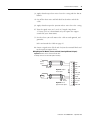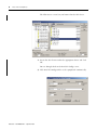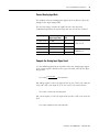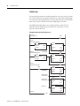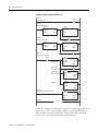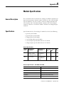
1
SLC 500 Fast Analog
I/O Module
Catalog Numbers 1746-FIO4I and
1746-FIO4V
User Manual
Important User Information
Solid state equipment has operational characteristics differing from those of
electromechanical equipment. Safety Guidelines for the Application,
Installation and Maintenance of Solid State Controls (publication SGI-1.1
available from your local Rockwell Automation sales office or online at
http://literature.rockwellautomation.com) describes some important
differences between solid state equipment and hard-wired electromechanical
devices. Because of this difference, and also because of the wide variety of
uses for solid state equipment, all persons responsible for applying this
equipment must satisfy themselves that each intended application of this
equipment is acceptable.
In no event will Rockwell Automation, Inc. be responsible or liable for
indirect or consequential damages resulting from the use or application of
this equipment.
The examples and diagrams in this manual are included solely for illustrative
purposes. Because of the many variables and requirements associated with
any particular installation, Rockwell Automation, Inc. cannot assume
responsibility or liability for actual use based on the examples and diagrams.
No patent liability is assumed by Rockwell Automation, Inc. with respect to
use of information, circuits, equipment, or software described in this manual.
Reproduction of the contents of this manual, in whole or in part, without
written permission of Rockwell Automation, Inc., is prohibited.
Throughout this manual, when necessary, we use notes to make you aware
of safety considerations.
WARNING
IMPORTANT
ATTENTION
Identifies information about practices or circumstances that can cause
an explosion in a hazardous environment, which may lead to personal
injury or death, property damage, or economic loss.
Identifies information that is critical for successful application and
understanding of the product.
Identifies information about practices or circumstances that can lead
to personal injury or death, property damage, or economic loss.
Attentions help you identify a hazard, avoid a hazard, and recognize
the consequence
SHOCK HAZARD
Labels may be on or inside the equipment, for example, a drive or
motor, to alert people that dangerous voltage may be present.
BURN HAZARD
Labels may be on or inside the equipment, for example, a drive or
motor, to alert people that surfaces may reach dangerous
temperatures.
Rockwell Automation, Allen-Bradley, TechConnect, RSLogix500, SLC, SLC 500, and SLC 5/02 are trademarks of Rockwell
Automation, Inc.
Trademarks not belonging to Rockwell Automation are property of their respective companies.
Table of Contents
Preface
About This Publication . . . . .
Who Should Use This Manual
Additional Resources. . . . . . .
Conventions . . . . . . . . . . . . .
.
.
.
.
.
.
.
.
.
.
.
.
.
.
.
.
.
.
.
.
.
.
.
.
.
.
.
.
.
.
.
.
.
.
.
.
.
.
.
.
.
.
.
.
.
.
.
.
.
.
.
.
.
.
.
.
.
.
.
.
.
.
.
.
.
.
.
.
.
.
.
.
.
.
.
.
.
.
.
.
.
.
.
.
.
.
.
.
.
.
.
.
.
.
.
.
5
5
6
6
Chapter 1
Quick Start
Required Tools and Equipment . . . . . . . . . . . . . . . . . . . . . . . 7
Procedures . . . . . . . . . . . . . . . . . . . . . . . . . . . . . . . . . . . . . . 8
Chapter 2
Install and Wire the Modules
Determine the Module’s Power Requirements . . .
Determine Compatibility with Other I/O Modules.
Configure Input Channels . . . . . . . . . . . . . . . . . .
Select the I/O Rack Slot. . . . . . . . . . . . . . . . . . . .
Install the Module . . . . . . . . . . . . . . . . . . . . . . . .
Considerations When Wiring . . . . . . . . . . . . . . . .
Minimize Electrical Noise Interference . . . . . . . . .
Wire the Module . . . . . . . . . . . . . . . . . . . . . . . . .
Minimize Ground Loops . . . . . . . . . . . . . . . . . . .
Label the Terminal Block. . . . . . . . . . . . . . . . . . .
.
.
.
.
.
.
.
.
.
.
.
.
.
.
.
.
.
.
.
.
.
.
.
.
.
.
.
.
.
.
.
.
.
.
.
.
.
.
.
.
.
.
.
.
.
.
.
.
.
.
.
.
.
.
.
.
.
.
.
.
.
.
.
.
.
.
.
.
.
.
.
.
.
.
.
.
.
.
.
.
11
12
13
14
14
16
18
18
20
21
Chapter 3
Access Files to Configure I/O
Click and Drag Configuration . . . . . . . . . . . . . . . . . . . . . . . 23
Read IO Config Method. . . . . . . . . . . . . . . . . . . . . . . . . . . . 24
Chapter 4
Processor and Module
Considerations
Processor Considerations. . . . . . . . . . . . . . . . . . . . . . . . . . . 30
Module Considerations . . . . . . . . . . . . . . . . . . . . . . . . . . . . 32
Chapter 5
Write Ladder Logic
3
Retentive and Non-retentive Programming . . . . . . . . . . . . . .
Detect an Out-of-range Input. . . . . . . . . . . . . . . . . . . . . . . .
Overview of Scaling Inputs and Outputs . . . . . . . . . . . . . . .
Scale an Analog Input and Detect an Out-of-range Condition
Scale an Analog Output. . . . . . . . . . . . . . . . . . . . . . . . . . . .
Scale Offsets When >32,767 or <32,768. . . . . . . . . . . . . . . .
Range-check an Analog Input and Scale It for an Output . . .
PID Control with Analog I/O Scaling . . . . . . . . . . . . . . . . . .
39
41
42
44
47
49
52
56
Publication 1746-UM009B-EN-P - September 2007
4
Table of Contents
Chapter 6
Calibrate the Module
Calibration Tradeoffs . . . . . . . . . . . . . . . . . . . . . . . . . . . . . . 61
Calibrate an Analog Input Channel . . . . . . . . . . . . . . . . . . . 62
Chapter 7
Test Module Operation
Test the SLC 500 System . . . . . . . . . . . . . . . . . . . . . . . . . . . 67
Test the Module . . . . . . . . . . . . . . . . . . . . . . . . . . . . . . . . . 67
Chapter 8
Maintenance and Safety
Preventive Maintenance. . . . . . . . . . . . . . . . . . . . . . . . . . . . 75
Safety Considerations When Troubleshooting . . . . . . . . . . . . 76
Appendix A
Module Specifications
General Description . . . . . . . . . . . . . . . . . . . . . . . . . . . . . . 77
Specifications . . . . . . . . . . . . . . . . . . . . . . . . . . . . . . . . . . . 77
Appendix B
2’s-complement Binary Numbers
Use 2’s-complement Binary Numbers. . . . . . . . . . . . . . . . . . 83
Appendix C
Module Input and Output Circuits
. . . . . . . . . . . . . . . . . . . . . . . . . . . . . . . . . . . . . . . . . . . . . 87
Index
Publication 1746-UM009B-EN-P - September 2007
Preface
About This Publication
Read this preface to familiarize yourself with the rest of the manual.
This preface covers the following topics:
•
•
•
•
•
Who should use this manual
The purpose of this manual
Terms and abbreviations
Conventions used in this manual
Allen-Bradley support
This manual is a reference guide for the 1746-NR4 RTD/Resistance
Input Module. The manual:
• gives you an overview of system operation.
• explains the procedures you need to install and wire the module
at the customer site.
• provides ladder programming examples.
• provides an application example of how this input module can
be used to control a process.
Who Should Use This
Manual
Use this manual if you are responsible for designing, installing,
programming, or troubleshooting control systems that use
Allen-Bradley small logic controllers.
You should have a basic understanding of SLC 500 products. You
should understand programmable controllers and be able to interpret
the ladder logic instructions required to control your application. If
you do not, contact your local Allen-Bradley representative for
information on available training courses before using this product.
5
Publication 1746-UM009B-EN-P - September 2007
6
Preface
Additional Resources
The following documents contain information that may be helpful to
you as you use Allen-Bradley SLC products.
Resource
Description
SLC 500 Systems Selection Guide, publication 1747-SG001
An overview of the SLC 500 family of products
SLC 500 Module Hardware Style User Manual, publication
1747-UM011
A description on how to install and use your modular SLC 500
programmable controller
Installation & Operation Manual for Fixed Hardware Style
Programmable Controllers, publication 1747-6.21
A description on how to install and use your fixed SLC 500
programmable controller
SLC 500 Instruction Set Reference Manual, publication
1747-RM001
A reference manual that contains status file data, instruction set,
and troubleshooting information about the software
SLC 500 4-Channel Analog I/O Modules User’s Manual, publication
1746-UM005
A resource manual and user’s guide containing information about
the analog modules used in your SLC 500 system.
Industrial Automation Wiring and Grounding Guidelines, publication In-depth information on grounding and wiring Allen-Bradley
1770-4.1
programmable controllers
Application Considerations for Solid-State Controls. publication
SGI-1.1
A description of important differences between solid-state
programmable controller products and hard-wired
electromechanical devices
National Electrical Code, published by the National Fire Protection
Association of Boston, MA
An article on wire sizes and types for grounding electrical
equipment
You can view or download publications at
http://literature.rockwellautomation.com. To order paper copies of
technical documentation, contact your local Rockwell Automation
distributor or sales representative.
Conventions
The following conventions are used throughout this manual:
• Bulleted lists such as this one provide information, not
procedural steps.
• Numbered lists provide sequential steps or hierarchical
information.
Publication 1746-UM009B-EN-P - September 2007
Chapter
1
Quick Start
This chapter presents an overview of installation and start-up
procedures to help you get the module working quickly.
It refers to full procedures in corresponding chapters of this manual or
in other SLC documentation that may be helpful if you are unfamiliar
with programming techniques or system installation.
We recommend that you use this chapter in either of two ways.
• Use as a fast installation and start-up guide for the experienced
users.
• Use as an overview for using the entire manual for the first-time
user.
IMPORTANT
Required Tools and
Equipment
7
If you have any questions about the abbreviated procedures
presented in this chapter, always read the referenced chapters
and other recommended documentation before trying to apply
the information.
Have the following tools and equipment ready.
•
•
•
•
•
•
•
•
•
•
Medium flat-head screwdriver
Medium Phillips-head screwdriver
Wire strippers
Utility knife
Hot-air blower
Shrink wrap
Belden 8761 cable or equivalent
Analog I/O devices for your application
I/O modules (1746-FIO4I and/or 1746-FIO4V)
Programming software
Publication 1746-UM009B-EN-P - September 2007
8
Quick Start
Procedures
Follow these steps to get your module running in your SLC system.
1. Plan the inclusion of analog I/O modules in your SLC system.
If a new system, specify the type of processor, number of I/O
racks, I/O modules, and power supply. If adding to an existing
system:
• assign modules to slot locations in the I/O rack.
• verify that the power supply for the I/O rack can handle the
increased load.
See SLC 500 Systems Selection Guide, publication 1747-SG001,
for more information.
2. Configure module input channels for current or voltage
operation.
Locate the 2-switch assembly on the module’s circuit board, and
set each channel as follows.
Current (ON)
O
N
12
Switch 1 = Channel 0
Switch 2 = Channel 1
Voltage (OFF)
3. Connect I/O devices with cables.
IMPORTANT
• Connect only one end of the cable shield to earth ground.
• Channels are not isolated from each other. All analog commons are
connected together internally.
• The module does not provide loop power for analog inputs.
• Use a power supply that matches the transmitter (sensor)
specifications.
Refer to Install and Wire the Modules on page 11.
Publication 1746-UM009B-EN-P - September 2007
Quick Start
9
For Differential Inputs
Module
Analog +
Sensor –
Earth
Ground
Important: Jumper
unused inputs.
Load
Earth
Ground
Important: Do not
jumper unused outputs.
For Single-ended Input
with 3-wire Transmitter
Transmitter
Supply
Signal
GND
0
1
2
IN 0 +
IN 0 –
ANL COM
3
4
5
IN 1 +
IN 1 –
ANL COM
6
7
8
Not Used
OUT 0
ANL COM
9
10
11
Not Used
OUT 1
ANL COM
Module
Power +
Supply –
3
4
5
IN +
IN –
ANL COM
4. Configure the system I/O and module ID.
With the software, configure the processor, I/O racks, slots, and
I/O modules.
When assigning an I/O module to a slot location, select the
module from the displayed list. If not listed, select OTHER at the
bottom of the list and enter the module’s ID code at the prompt.
ID code for 1746-FIO4I is 3224
ID code for 1746-FIO4V is 3218
5. Understand A/D & D/A converter resolution on input and
output words.
The module’s I/O channel converters limit bit usage to less than
a full 16-bit word.
The input channel converter resolution is 12 bits, where the
highest four bits are always zero.
The output channel converter resolution is 14 bits, where the
lowest two bits are never used.
Publication 1746-UM009B-EN-P - September 2007
10
Quick Start
The lowest two bits have no effect on the output value.
Refer to Processor and Module Considerations on page 29 for
more information.
SLC 500 Processor
Data Files
Input Image
(2 words)
Address
Channel 0 Input Word
I:1.0
Channel 1 Input Word
I:1.1
Output Image
(2 words)
lsb
msb (variable input data)
0 0 0 0
Bit 15
Bit 11
Bit 0
Address
O:1.0
Channel 0 Output Word
Channel 1 Output Word
O:1.1
msb
variable output data)
lsb
X X
Bit 2 Bit 0
Bit 15
X = not used
6. Write ladder logic to process the module’s analog data.
We provide several programming examples that include the
following:
•
•
•
•
•
•
Clear the output when changing mode or cycling power
Detect an out-of-range input
Scale analog outputs
Scale offsets
Scale and range-check analog inputs and outputs
PID control with analog I/O scaling
Study these examples to understand how to program the
module.
Refer to Write Ladder Logic on page 39.
7. (Optional) Write ladder logic to maintain calibrated inputs.
We show you how to write ladder logic that provides a
calibrated input reference during runtime, and lets you
periodically calibrate module inputs. We suggest that you modify
the logic examples to suit your application and add them to your
application program.
Refer to Calibrate the Module on page 61 for more information.
Publication 1746-UM009B-EN-P - September 2007
Chapter
2
Install and Wire the Modules
This chapter describes procedures to install fast analog I/O modules in
an SLC 500 system. The procedures include the following tasks.
•
•
•
•
•
•
•
•
•
•
Determine the Module’s
Power Requirements
determine the module’s power requirements
determine compatibility with other I/O modules
configure input channels
select the I/O rack slot
install the module
consider when wiring
– using system wiring guidelines
– grounding the cable
– determining cable length
minimize electrical noise interference
wire the module
minimize ground loops
label the terminal block
Analog modules require power from the 5V dc and 24V dc backplane
power supplies of the SLC 500 system. This table shows the backplane
power requirements for fast analog I/O modules.
Current Load
Catalog Number
Current at 5V dc
Current at 24V dc
1746-FIO4I
55 mA
150 mA
1746-FIO4V
55 mA
120 mA
Use this table to compute the module’s portion of total load on the
modular system power supply.
For more information, refer to SLC 500 Systems Selection Guide,
publication 1747-SG001.
11
Publication 1746-UM009B-EN-P - September 2007
12
Install and Wire the Modules
Determine Compatibility
with Other I/O Modules
Use the I/O Compatibility chart when using the expansion rack of a
fixed controller (1747-L20, 1747-L30, and 1747-L40). The chart
determines compatibility of other I/O modules with fast analog
modules. Compatibility is solely based on current drawn from the
backplane.
For more information, refer to the SLC 500 Fixed Hardware Style
Installation and Operation Manual, publication 1747-6.21.
I/O Compatibility
1746-FIO4I
1746-FIO4V
1746 Module
FIO4I
FIO4V
• (1)
•
IA4, IA8, IA16
•
•
IB8, IB16
•
•
IB32
•
•
IG16
•
•
IM4, IM8, IM16
•
•
IN16
•
•
IO4
•
IO8
IO12
•
•
ITB16, ITV16
•
•
IV8, IV16, IV32
NIO4I, NIO4V
∇ (2)
∇
NO4I, NO4V
NI4
•
•
NR4
•
•
NT4
•
•
OA8
OA16
•
•
OB8
OB16, OB32
•
OBP16
•
•
OG16
•
•
OV8
•
OV16
OV32
Publication 1746-UM009B-EN-P - September 2007
Install and Wire the Modules
13
I/O Compatibility
1746-FIO4I
1746-FIO4V
1746 Module
•
OW4
OW8, OW16
OX8
•
BASIC
BASn
DCM
HS
•
KE
KEn
Configure Input Channels
(1)
The • symbol indicates an allowable combination of 1746 I/O modules.
(2)
The ∇ symbol indicates an auxiliary 24V dc power supply may be needed.
Your fast analog I/O modules have a two-switch assembly to
configure the input channels for either current or voltage operation.
The switches are on the module’s circuit board. Switch orientation is
shown on the nameplate of the module.
Switch Orientation
ON – Configures channel for current input
OFF – Configures channel for voltage input
Switches labeled 1 and 2 control the input mode of channels 0 and 1
respectively.
Channels 0 and 1 Input Mode
Current (ON)
O
N
12
Switch 1 = Channel 0
Switch 2 = Channel 1
Voltage (OFF)
Publication 1746-UM009B-EN-P - September 2007
14
Install and Wire the Modules
Select the I/O Rack Slot
Two factors determine where you should locate the module in the
I/O rack: ambient temperature and electrical noise. Consider the
following conditions when selecting an I/O rack slot for the module.
Position the module:
• in a slot away from ac or high voltage dc modules.
• away from the rack power supply if installed in a modular system.
• in the I/O rack lowest in the enclosure for a cooler ambient.
Install the Module
When installing the module in an I/O rack, you do not need to remove
the terminal block from the module. However, if the terminal block is
removed, use the write-on label located on the side of the terminal
block to identify the module location and type. To remove the terminal
block, grasp it on the top and bottom and pull outward and down.
ATTENTION
IMPORTANT
Never install, remove, or wire modules with power applied to
the I/O rack. Rid yourself of electrostatic charge before
handling the module. Electrostatic discharge can degrade
module performance or destroy analog circuitry.
Do not tamper with the module’s factory-sealed potentiometer.
It does not require any adjustments.
Follow these steps when installing or removing the module.
1. Verify that input configuration switches 1 and 2 are set correctly.
ATTENTION
Take care to avoid connecting a voltage source to a channel
configured for current input. This could result in improper
module operation or damage to the module.
2. Align the module’s circuit board with the rack’s card guide.
See Installing the Module on page 15.
3. Slide the module in until top and bottom retaining clips are
secured.
Publication 1746-UM009B-EN-P - September 2007
Install and Wire the Modules
15
4. To remove the module, press the retaining clips at the top and
bottom of the module and slide the module out.
Installing the Module
Card Guide
Self-locking tabs secure the
module in the I/O rack.
Publication 1746-UM009B-EN-P - September 2007
16
Install and Wire the Modules
Considerations When
Wiring
This section provides guidelines on wiring the system, grounding the
cables, determining cable length.
ATTENTION
Before wiring the module, disconnect SLC system power, I/O
rack power, and module power.
System Wiring Guidelines
Use the following guidelines in planning the system wiring to the
module.
• Analog common terminals (ANL COM) are electrically
interconnected inside the module, but not internally connected
to earth.
• Voltages on IN+ and IN– terminals must be within 0…20V with
respect to ANL COM to ensure proper input channel operation.
This is true for current and voltage input channel operation.
• Voltage outputs (OUT 0 and OUT 1) of the 1746-FIO4V module
are referenced to ANL COM. Load resistance (R1) for a voltage
output channel must be equal to or greater than 1 KΩ.
• Current output channels (OUT 0 and OUT 1) of the 1746-FIO4I
module source current that returns to ANL COM. Load resistance
(R1) for a current output channel must be within 0…500 Ω.
• Input connections for single-ended or differential input are the
same.
Publication 1746-UM009B-EN-P - September 2007
Install and Wire the Modules
17
Ground the Cable
Signal cable such as Belden cable #8761 (or equivalent) has two signal
wires (black and clear), one drain wire, and a foil shield. The drain
wire and foil shield must be grounded at only one end of the cable,
not at both ends.
Typical Signal Cable
Foil Shield
Shrink Wrap
Black Wire
Insulation
Clear Wire
IMPORTANT
Drain Wire
Ground the cable shield at one end having a good earth-ground
connection, such as at an I/O chassis mounting bolt or nearest
ground bus in the I/O enclosure. Make this connection as short
as possible. Do not ground the cable at the module’s terminal
block.
Determine Cable Length
When you determine the length of cable required to connect an I/O
device, remember to include additional length to route the drain wire
and foil shield to earth ground. Route your cable long enough to
avoid areas of high radiated electrical noise, but short enough to avoid
signal attenuation.
Publication 1746-UM009B-EN-P - September 2007
18
Install and Wire the Modules
Minimize Electrical Noise
Interference
Because high-speed analog signals are particularly vulnerable to
electrical noise, take precautions when routing your signal cables. To
help reduce the effects of electrical noise on analog signals, we
recommend that you do the following:
•
•
•
•
•
Install the SLC 500 system in a NEMA rated enclosure.
Make sure that the SLC 500 system is properly grounded.
Use Belden cable #8761 (or equivalent) for signal wiring.
Ground the cable properly.
Route signal cables away from other wiring or in grounded
conduit.
• Group these modules away from ac or high-voltage dc modules.
We recommend re-checking system operation after installing new
machinery or other sources of electrical noise near the system.
For additional information on this subject, refer to Industrial
Automation Wiring and Grounding Guidelines, publication 1770-4.1.
Wire the Module
Follow this procedure when wiring your modules.
ATTENTION
Before wiring a module, disconnect power from the SLC 500
system and from any other source to the module.
1. Strip about 7.6 cm (3 in.) of casing to expose the wires at each
end of the cable.
2. Twist the drain wire and foil shield together and bend them
away from the cable at the grounded end of the cable.
Grounded End
Twisted Foil Shield and Drain Wire
Black Wire
Casing
Shrink Wrap
Clear Wire
Ungrounded End
Black Wire
Casing
Publication 1746-UM009B-EN-P - September 2007
Shrink Wrap
Clear Wire
Install and Wire the Modules
19
3. Apply shrink wrap where wires leave the casing with the hot-air
blower.
4. Cut off the drain wire and foil shield at the other end of the
cable.
5. Apply shrink wrap to the junction where wires leave the casing.
6. Trim the signal wires to 5 cm (2 in.) lengths. Strip about
4.76 mm (3/16 in.) of insulation away to expose the copper
strands for your connections.
7. Decide where you will connect the cable to earth ground, and
ground it.
Refer to Ground the Cable on page 17.
8. Connect signal wires (black and clear) to the terminal block and
to the input or output device.
Wiring Diagram for Module, Sensor, and Load (showing differential inputs)
Important: Channels are not isolated from each other.
All analog commons are connected together internally.
+
Analog
Sensor
–
Earth
Ground
Important: Jumper
unused inputs.
Load
Earth
Ground
Important: Do not
jumper unused outputs.
0
1
2
IN 0 +
IN 0 –
ANL COM
3
4
5
IN 1 +
IN 1 –
ANL COM
6
7
8
not used
OUT 0
ANL COM
9
10
11
not used
OUT 1
ANL COM
Publication 1746-UM009B-EN-P - September 2007
20
Install and Wire the Modules
IMPORTANT
Single-ended inputs are less immune to noise than are
differential inputs.
Wiring Schematic for Single-ended Current-loop Analog Input Connections
Important: The module does not provide loop power for analog inputs.
Use a power supply that matches the transmitter specifications.
2-wire Transmitter
Transmitter
+
–
Power +
Supply –
3-wire Transmitter
Transmitter
Supply
Signal
GND
Power +
Supply –
4-wire Transmitter
Power +
Supply –
Transmitter
Supply
Signal
+
+
–
–
Module
IN +
IN –
ANL COM
Module
IN +
IN –
ANL COM
Module
IN +
IN –
ANL COM
9. Repeat steps 1…6 for each channel. For each unused input
channel, jumper together the plus (+), minus (–), and common
(ANL COM) terminals. For each unused output channel, do not
connect terminals.
Minimize Ground Loops
To keep the ground-loop currents of input circuits to a minimum, we
recommend that you:
• use the same power supply to power both input channels of a
module.
• otherwise, tie together the grounds of separate power supplies.
See Wiring Schematic for Single-ended Current-loop Analog Input
Connections for more information.
Publication 1746-UM009B-EN-P - September 2007
Install and Wire the Modules
Label the Terminal Block
21
The terminal block has a write-on label. Use it to ensure that you
install the correct terminal block on the corresponding module.
Terminal Block
Note: The black dot on the label
indicates the position of terminal 0.
SLOT ____ RACK ____
MODULE _____
Publication 1746-UM009B-EN-P - September 2007
22
Install and Wire the Modules
Publication 1746-UM009B-EN-P - September 2007
Chapter
3
Access Files to Configure I/O
There are two ways to configure the SLC Chassis for a 1746-FIO4I/V
module. You can either click and drag items from the list or you can
use the Read IO Config method.
Click and Drag
Configuration
Follow these steps to configure the SLC chassis by clicking and
dragging modules.
1. Double-click the menu item to open the IO Configuration menu
in RSLogix500 software.
2. Place the 1746-FIO4I/V module into the correct slot by clicking
and dragging from the list.
23
Publication 1746-UM009B-EN-P - September 2007
24
Access Files to Configure I/O
The I/O Configuration is now complete. Each slot shows the
corresponding module that is located on the rack. In this
example the 1746-FIO4V is in slot 1.
Read IO Config Method
Follow these steps to configure the SLC chassis by using the Read IO
configuration method.
1. Double-click the menu item to open the IO Configuration menu
in RSLogix500 software.
Publication 1746-UM009B-EN-P - September 2007
Access Files to Configure I/O
25
2. Place the 1746-FIO4I/V module into the correct slot by clicking
Read IO Config.
The following screen appears.
3. Select either the driver and processor node number or use the
Who Active button to browse for the device.
• If you selected the driver and node number, proceed to step 5.
• If you clicked Who Active, the following screen appears.
Publication 1746-UM009B-EN-P - September 2007
26
Access Files to Configure I/O
The Who Active screen lets you browse for the SLC device.
4. Locate the SLC Chassis under the appropriate driver and click
OK.
You are brought back to the Read IO Config screen.
5. Click Read IO Config and the rack is populated automatically.
Publication 1746-UM009B-EN-P - September 2007
Access Files to Configure I/O
27
The I/O Configuration is now complete. Each slot shows the
corresponding module on the rack. In this example the
1746-FIO4V is in slot 1.
Publication 1746-UM009B-EN-P - September 2007
28
Access Files to Configure I/O
Publication 1746-UM009B-EN-P - September 2007
Chapter
4
Processor and Module Considerations
This chapter describes concepts that you need to understand to
program the fast analog I/O module in an SLC 500 system.
The following are processor considerations.
• Update processor analog I/O data
• Monitor analog I/O data
• Address I/O image words
The following are module considerations.
•
•
•
•
•
•
•
•
•
•
29
Resolve data of the module’s I/O channel converters
Convert analog input data
Compute the analog input signal level
Convert analog output data
Compute the analog output
Filter input channel
Compute time delay for A/D conversion
Determine response to slot disable
Determine safe state for outputs
Enter module ID code
Publication 1746-UM009B-EN-P - September 2007
30
Processor and Module Considerations
Processor Considerations
Knowing how the processor works helps you program it more
effectively.
Processor Update of Analog I/O Data
Analog input and output image words are updated by the processor
once every processor scan when the processor scans data and
program files in succession.
Processor scan time depends largely on the size of your program files:
the greater the number of programming instructions, the longer the
time to scan the file. Some instructions take longer to scan than
others.
For information on processor scan time and instruction execution
time, refer to the SLC 500 Instruction Set Reference Manual,
publication 1747-RM001.
If an application requires processor updates of analog data more
frequently than once per scan, use Immediate Input or Immediate
Output instructions. These instructions typically update an analog
channel in 1 ms, but also increase the overall scan time by the same
amount.
Typical update times for SLC processors are:
• ~
– 10 ms for a typical 1K program.
• 1 ms per analog channel when using immediate I/O instructions.
Monitor Analog I/O Data
You can monitor analog input and output data in binary or decimal
format. You select the format by its radix. The default radix is binary.
Binary data is presented in 2’s-complement format. Changing the radix
to decimal lets you view analog I/O data as decimal representations of
integer words.
Refer to 2’s-complement Binary Numbers on page 83 for more
information.
Publication 1746-UM009B-EN-P - September 2007
Processor and Module Considerations
31
Address I/O Image Words
Each module input channel is addressed as a single word in the
processor’s input image table and each module output channel is
addressed as a single word in the processor’s output image table. The
module uses a total of two input words and two output words.
Processor I/O Image Words Used by the Module
Word Addresses
in I/O Image File
Bit 15
Output Image
Analog Input
Sensors
Bit 15
Output
Scan
O:e.0
O:e.1
Input Module’s
A/D Converter
Bit 0
Analog Output
Devices
Output Channel 0
Output 0
Output Channel 1
Output 1
Bit 0
Input 0
Input Channel 0
Input 1
Input Channel 1
Input
Scan
Input Image
I:e.0
I:e.1
e = module’s slot number in I/O rack
The converted input values from input channels 0 and 1 are addressed
as words 0 and 1 of the slot where the module resides. The output
values for the output channels 0 and 1 are addressed as output words
0 and 1 of the slot where the module resides.
EXAMPLE
You would address the output image word for output O, word 0,
in slot 3 as: O:3.0 where delimiters : and . must be placed as
shown.
module’s I/O rack slot location
Capital Letter
I = Input, or
O = Output
I/O image table word
O:e.0-4
delimiters
Publication 1746-UM009B-EN-P - September 2007
32
Processor and Module Considerations
Module Considerations
The module’s I/O channel converters affect resolution of I/O data and
bit usage in I/O image words. We show you how to compute I/O
signal levels. Input filtering and input A/D conversion affect input
response time.
Data Resolution of the Module’s I/O Channel Converters
The module’s I/O channel converters limit bit usage to less than a full
16-bit word when converting analog to digital input data and digital to
analog output data. Bit maps show resulting digital data storage in
input and output image words.
Bit Usage for I/O Channel Converters
msb
I:e.0
I:e.1
0
0
0
0
15
14
13
12
0
0
0
0
15
14
13
12
Isb
CH 0 INPUT
11
10
9
11
10
9
8
7
6
5
4
3
2
1
0
6
5
4
3
2
1
0
CH 1 INPUT
8
7
Isb
msb
O:e.0
Bits not used
CH 0 OUTPUT
15
14
13
12
11
10
9
15
14
13
12
11
10
9
O:e.1
8
7
6
5
4
3
2
6
5
4
3
2
7
0
Bits not used
CH 1 OUTPUT
8
1
1
0
e = module’s slot number
The input channel converter resolution is 12 bits, where the highest
four bits are always zero. The usable range of the channel word is
0…4095.
The output channel converter resolution is 14 bits, where the lowest
two bits are not used. They have no effect on the output value.
IMPORTANT
The module left-justifies the 14-bit data (lsb at bit 2) in the
output channel word. This reduces the output resolution to:
• 2.56348 µA/LSB for current outputs
• 1.22070 mV/SLB for voltage outputs
Publication 1746-UM009B-EN-P - September 2007
Processor and Module Considerations
33
Convert Analog Input Data
The module converts analog input signals to 12-bit binary values for
storage in the input image table.
The decimal range, number of significant bits, and converter
resolution depend on the input range that you use for the channel.
Input Range
Decimal Range
(input image table)
Significant
Bits
0…10V – 1LSB
0…4095
12
0…5V
0…2047
11
1…5V
409…2047
10
0…20 mA
0…2047
11
4…20 mA
409…2047
10
Nominal Resolution
2.4414 mV/LSB
9.7656 µA/LSB
Compute the Analog Input Signal Level
Use the following formula to determine what the analog input signal
level (sensor signal) should be for a given decimal value in the input
image table.
Full Scale Input
Sensor Signal =
Full Scale Count
x Input Image Value
For voltage inputs, a full scale input of 10V dc has a full scale count of
4095 and a full scale input of 5V dc has a full scale count of 2047.
Sensor Signal = 2.44 mV/count x Input Image Value
For current inputs, a full scale input of 20 mA has a full scale count of
2047.
Sensor Signal = 0.00977 mA/count x Input Image Value
Publication 1746-UM009B-EN-P - September 2007
34
Processor and Module Considerations
For example, if the input image table value is 409 from a 4…20
mA sensor.
EXAMPLE
Full Scale Input
Sensor Signal =
Full Scale Count
x Input Image Value = 0.00977 x 409 = 4 mA
Convert Analog Output Data
The module converts 16-bit binary values from the output image table
to 14-bit analog output signals and left-justifies the bit code in the
channel word. The output range, decimal representation for the
output range, number of significant bits, and converter resolution are
as shown in the following table.
Analog Output Data
Module Output Range
Decimal
Significant
Representation
Bits
(output image table)
FIO4I
0…21 mA – 1LSB
0…+32,764
13 bits
0…20 mA
0…+31,208
12.92 bits
4…20 mA
6242…31,208
12.6 bits
–10…+10V dc –
1LSB
–32,768…+32,764
14 bits
0…10V dc – 1LSB
0…32,764
13 bits
0…5V dc
0…16,384
12 bits
1…5V dc
3277…16,384
11.67 bits
FIO4V
Resolution
2.56348 µA/LSB
1,22070 mV/LSB
Compute the Analog Output
Use the following formula to compute the output image-table value
(decimal representation) required for a desired analog-output signal
level (to the output device).
Output Image Value =
Publication 1746-UM009B-EN-P - September 2007
Full-scale Decimal Representation
x Desired Signal Level
Full-scale Output
Processor and Module Considerations
If the module’s output range is 4…20 mA and you want to set
the output to 4 mA, compute the output image value as follows.
EXAMPLE
Output Image Value =
31,208
~
20 mA x 4 mA – 6242
The actual resolution for analog current outputs is 2.56348
µA/LSB, where the 14-bit decimal representation is left
justified as follows.
IMPORTANT
msb
Isb
CHANNEL OUTPUT WORD
15
14
13
12
11
10
9
8
7
6
Bits not
5
4
3
2
1
0
Use the following formula to compute the output image value if
the module’s output range is 1…5V dc and you want to set the
output to 1V dc.
EXAMPLE
Output Image Value =
16,384
~
5V dc x 1V dc – 3277
The actual resolution for analog voltage outputs is 1.22070
mV/LSB, where the 14-bit decimal representation is left
justified as follows.
IMPORTANT
msb
Isb
Bits not used
Channel Output Word
15
35
14
13
12
11
10
9
8
7
6
5
4
3
2
1
0
Publication 1746-UM009B-EN-P - September 2007
36
Processor and Module Considerations
Input Channel Filtering
The module’s input filters are designed to attenuate less than 1% of
the input signal in the 0…1000 Hz range.
Percent of Signal Passed
100
99.9
99.8
Percent of Signal
99.7
99.6
99.5
99.4
99.3
99.2
99.1
99
0
100
300
500
1000
The –3dB point is approximately 7000 Hz. The input filter causes a
signal delay of approximately 100 µs. The module’s A/D converter
sees a 95% step change of an input signal in that time.
Input Channel Frequency Response
0
Attenuation in dB
–4
–8
–12
–16
–20
–24
–28
–32
–36
–40
103
Publication 1746-UM009B-EN-P - September 2007
104
Frequency in Hz
105
Processor and Module Considerations
37
Time Delay for A/D Conversion
The A/D converter uses 7.5 µs for data conversion, 248.5 µs for data
settling, and 256 µs for data transfer to the backplane. New data is
available in 512 µs cycles.
Response Time of A/D Converter
Start
Data
conversion
Data
settling
7.5 µs
248.5 µs
Data transfer to
the backplane
Data ready for
processor read
256 µs
512 µs
Worst case point for a change of input to occur.
This results in a 1.1ms delay for the processor to read a step change.
The worst-case specification for the SLC processor to read a step
change is 1.1ms between readings. This is true for a step change
occurring just after data conversion (first 7.5 µs of the 512 µs cycle). In
this case, the read cycle cannot begin until the next data conversion.
IMPORTANT
Do not attempt to read data from the module more often than
once every 512 µs. If you do, the module may not be able to
update new data.
Response to Slot Disable
You can disable any I/O rack slot by means of a processor function.
Before disabling a slot containing an analog I/O module, be aware of
the implications.
ATTENTION
Clearly understand the safety implications of disabling an
analog module slot before doing it.
Publication 1746-UM009B-EN-P - September 2007
38
Processor and Module Considerations
Input Response to Slot Disable
The module continues to update its inputs for transfer to the
processor, but the processor:
• does not read inputs from the module in a disabled slot.
• retains the last-state input image table values.
• upon re-enabling the slot, reads current inputs in the subsequent
scan.
Output Response to Slot Disable
While the module holds its outputs in their last state, the processor:
• may update its output image table.
• does NOT transfer output image table values to the module.
• upon re-enabling, transfers the current output image in the
subsequent scan.
Safe State for Outputs
Whenever an SLC 500 system is not in RUN mode, the analog
module’s outputs are automatically forced to 0V or 0 mA by the
SLC 500 system. This occurs when the processor is in one of the
following modes:
• Fault
• Program
• Test
ATTENTION
When designing and installing the SLC 500 system, place
devices connected to analog output channels in a safe state
whenever the analog output is zero (± the offset error).
Determine which output conditions must be held ON for a safe
state.
Module ID Code
You must enter the ID code if your programming software does not
include the subject I/O module in its list of modules.
ID code for FIO4I is 3224
ID code for FIO4V is 3218
Publication 1746-UM009B-EN-P - September 2007
Chapter
5
Write Ladder Logic
This chapter presents these programming examples.
•
•
•
•
•
•
Retentive and non-retentive programming
Detect an out-of-range input
Scale analog inputs and detect an out-of-range condition
Scale analog outputs
Scale offsets when > 32,767 or < –32,768
Scale and range-check analog inputs and outputs
• PID xontrol with analog I/O scaling
IMPORTANT
Retentive and Non-retentive
Programming
We present programming examples for instructional purposes
only. Because of the many variables and requirements
associated with any application, Rockwell Automation cannot
assume responsibility or liability for actual use based on these
examples.
The processor’s automatic response for scanning the I/O image table
is described below.
Processor Automatic Response
Conditions
• Mode is switched to Program
• Power is turned OFF
• Mode is switched to Run
• Power is turned ON
39
Processor Response
Retains the last values in the I/O image
table
Transfers output image data to the module
and input image data from the module
• Processor detects a minor fault
Resets analog outputs to zero, but retains
output image values
• Fault condition is corrected
Transfers output image data to the module
Publication 1746-UM009B-EN-P - September 2007
40
Write Ladder Logic
We give you the following examples for programming a different
response.
• Retentive analog output
• Non-retentive analog output
• Clear the output for changing mode or cycling power
Retentive Analog Output
This example loads a program constant into an analog output
channel. Consider a digital I/O module in slot 1, and an analog I/O
module in slot 2. When bit 0 of the digital I/O module is set, the rung
is true, and the full-scale value of 32,764 is moved into the output
image table location corresponding to slot 2, analog output channel 0.
At the end of the scan, the value is transferred to the module and
converted to a corresponding full-scale voltage or current output.
Retentive Example
I:1.0
][
0
MOV
MOVE
Source
Dest
32764
O:2.0
Non-retentive Analog Output
This example loads a program constant into an analog output channel
and clears it, based on logical conditions. Consider a digital I/O
module in slot 1, and an analog I/O module in slot 2. When bit 0 is set
in word 0 of the digital I/O module, the first rung is true and the
full-scale value of 32,764 is transferred to channel 0. When the bit is
reset to zero, the second rung is true, and the value of zero is
transferred to the channel.
Non-retentive Example
I:1.0
][
0
I:1.0
] /[
0
Publication 1746-UM009B-EN-P - September 2007
MOV
MOVE
Source
Dest
32764
O:2.0
MOVE
Source
Dest
0
O:2.0
Write Ladder Logic
41
Clear the Output for Changing Mode or Cycling Power
This example clears analog output channel 0 during the initialization
scan (first processor scan). The first pass bit, S2:1/15, in the Status File
is used to initialize the analog output when you apply power in the
RUN mode or upon setting the processor to the RUN or TEST mode.
This bit goes ON automatically only for the first-pass scan. To clear
another analog output channel, use another rung with a different
MOV destination address. The analog module is in slot 2.
S2:1/15
][
Detect an Out-of-range
Input
MOV
MOVE
Source
Dest
0
O:2.0
Analog modules do not provide an input out-of-range signal to the
processor. However, if this feature is critical to a specific application,
you can program the processor to provide this function.
The following program applies to all SLC 500 processors. It uses
comparison instructions (LES and GRT) to check for analog input
values which exceed low and high limits respectively. Whenever this
happens, the program latches a bit that could serve to trigger an alarm
elsewhere in your ladder program. In this example, the input range is
1…5V dc (decimal range of 409…2047).
MAIN
B3/0
(U)
B3/1
(U)
LES
LESS THAN
Source A
Source B
GRT
GREATER THAN
Source A
Source B
B3/0
(L)
I:1.0
409
B3/1
(L)
I:1.0
2047
Turn OFF Alarms
Turn ON Alarm,
Low Limit Exceeded
Turn ON Alarm,
High Limit Exceeded
Remainder of Program
END
Publication 1746-UM009B-EN-P - September 2007
42
Write Ladder Logic
We present an alternative program for SLC 5/02 (and later) processors.
It uses a single Limit Test instruction that checks low and high limits.
Whenever the input value exceeds a limit, this program latches a bit
that could trigger an alarm elsewhere in your ladder program. In this
example, the input range is 0…10V dc (decimal range of 0…4095). If
the input range were 4…20 mA, the low and high limits would be
2047 and 408, respectively.
MAIN
B3/0
(U)
LIM
LIMIT TEST (CIRC)
Low Lim
Test
High Lim
4095
I:1.0
408
B3/0
(L)
Turn OFF Alarm
Turn ON Alarm,
Limit Exceeded
Remainder of Program
END
In both examples, the analog input value is in word 0 of slot 1 (I:1.0).
Overview of Scaling Inputs
and Outputs
Scaling is the application of a ratio on the variable to be scaled, where
the ratio is the scaled range (Δy) to the input range (Δx).
The purpose for scaling values when programming analog I/O
modules is to change data format.
Scaling Inputs and Outputs
Publication 1746-UM009B-EN-P - September 2007
When you scale
You start with this data
format
And typically change the
format to
Inputs
Decimal input range in raw
counts (from the module’s A/D
converter)
Engineering units such as PSI
(stored in the data table)
Outputs
Integer values from the data
table (or from the input image
table)
Decimal output range in raw
counts to match the module’s
output range
On a linear graph
Δx
Δy
Write Ladder Logic
43
We illustrate input and output scaling, the source and type of data to
be scaled, and the type and destination of the scaled data.
Data Scaling
Input Scaling
Scaled Values
in Engineering
Units for Data
Table (Δy)
Output Scaling
Scaled Values
to Match
Module’s Raw
Counts
Module’s Input in
Raw Counts (Δx)
Sensor
Module
Input A/D
Input Raw
Signal
Counts
Range
from A/D
0…5V dc
0…2047
1…5V dc
409…2047
0…10V dc
0…4095
0…20 mA
0…2047
4…20 mA
409…2047
Integer Values (from Data
Table or Input Image)
Input Data Output
Image Table Image
Table
Table
Module
Input Raw D/A
Output
Counts to
Signal
D/A
Range
0…16,384
0…5V dc
3277…16,384
1…5V dc
0…32,764
0…10V dc
-32,768…32,764
-10 …10V
0…31,208
0…20 mA
6242…31,208
4…20 mA
0…32,764
0…21 mA
Output
Device
You scale data with ladder logic using arithmetic instructions such as
add, multiply, and double divide; or by using the scaling instruction
available with SLC 5/02 (or later) processors. The scaling computation
is as follows:
Scaled value = (input value x slope) + offset
Slope = Δy/Δx = scaled range / input range
= (scaled max. – scaled min.) / (input max. – input min.)
Offset = scaled min. – (input min. x slope)
In this context, the input value and input range are inputs to the
scaling function, not necessarily inputs associated with the sensor
input.
Publication 1746-UM009B-EN-P - September 2007
44
Write Ladder Logic
Scale an Analog Input and
Detect an Out-of-range
Condition
The following example shows input range checking and scaling the
analog input to engineering units for a 1746-FIO4V analog input
module.
We are making the following assumptions:
• The 1746-FIO4V module is located in slot 3 of a modular system.
• A pressure sensor with a 0…10V dc output is wired to input
channel 1.
• The sensor signal voltage is proportional to a range of
100…500 PSI.
• The process pressure must stay between 275…300 PSI.
(If the pressure deviates from this range, your logic sets an alarm
bit.)
• Data is presented in PSI for monitoring and display purposes.
Input Scaling
The scaling operation is displayed in the following graph. It displays
the linear relationship between the input and the resulting scaled
values.
Input Scaling
500 PSI
(scaled max)
Scaled
Value 300 PSI
275 PSI
Process operating range
100 PSI
(scaled min)
0 = 0V dc Low
(input min)
Limit
High
Limit
Input Value
Publication 1746-UM009B-EN-P - September 2007
4095 = 10V dc
(input max)
Write Ladder Logic
45
Calculate the Linear Relationship
Use the following equations to express the linear relationship between
the input value and the resulting scaled value.
Scaled value = (input value x slope) + offset
Slope = (scaled max – scaled min) / (input max – input min)
(500 – 100) / (4095 – 0) = 400/4095 = 0.0977
Offset = scaled min – (input min x slope)
(100 – (0 x [400/4095]) = 100
Scaled value = (input value x [0.0977]) + 100
Calculate the Out-of-range Limits
Use the following equation to compute low and high out-of-range
limits.
Input value = (scaled value – offset) / slope
~
– 1750 counts
high limit: (300 – 100) / (0.0977) ~
– 2750 counts
low limit: (275 – 100) / (0.0977)
Ladder Logic
We present two examples for programming the processor.
The first example uses standard math instructions available in any
SLC 500 processor. This ladder logic prevents a processor fault by
unlatching the mathematical overflow bit S2:5/0 before the end of the
scan.
The second example uses the scaling instruction (SCL) available in
SLC 5/02 (and later) processors. The rate parameter is calculated by
multiplying the slope by 10,000. If the slope exceeds 3.2767, you
cannot use the SCL instruction.
rate = (400/4095) x 10,000 = 977
(The slope is 0.0977 so you can use the SCL instruction.)
Publication 1746-UM009B-EN-P - September 2007
46
Write Ladder Logic
Standard Math Example
Rung 2:0
Check for below range
Rung 2:1
Check for above range
LES
LESS THAN
Source A
Source B
MUL
MULTIPLY
Source A
Source
Dest
Multiply by the
scaled range
Clear fault bit
from overflow
DDV
DOUBLE DIVIDE
Source A
Dest
Divide result
by input range
Rung 2:3
I:3.1
1750
GRT
GREATER THAN
Source A
I:3.1
Source B
2750
Rung 2:2
Scale the analog input
Add offset
Below-range
flag
B3/0
(L)
ADD
ADD
Source A
N7:0 contains
process pressure Source B
Dest
Above-range
flag
B3/1
(L)
I:3.1
400
N7:0
S2:5/0
(U)
4095
N7:0
N7:0
100
N7:0
END
Example Program Using the Scaling Instruction (SCL)
Rung 2:0
Check for below range
Rung 2:1
Check for above range
Rung 2:2
Scale the analog input
N7:0 contains
process
temperature
Below-range
flag
B3/0
(L)
LES
LESS THAN
Source A
Source B
I:3.1
1750
GRT
GREATER THAN
Source A
Source B
I:3.1
2750
SCL
SCALE
Source
Rate (/10000)
Offset
Dest
I:3.1
977
100
N7:0
Rung 2:3
END
Publication 1746-UM009B-EN-P - September 2007
Above-range
flag
B3/1
(L)
Write Ladder Logic
Scale an Analog Output
47
This example shows the scaling of analog output values to
engineering units for monitoring or controlling purposes.
We are making these assumptions.
• The FIO4I module is located in slot 2 of an SLC 500 system.
• An actuator of a flow control valve is wired to output channel 0.
• The actuator accepts a 4…20 mA signal for a 0…100% of valve
opening.
• The actuator can not receive a signal out of the 4…20 mA range.
• The percentage of valve opening is manually input to the SLC
processor.
This graph displays the linear relationship.
20mA = 31208
(scaled max.)
Scaled
Value
4mA = 6242
(scaled min.)
0%
(input min.)
Input Value
(from data table)
100%
(input max.)
Calculate the Linear Relationship
Use these equations to compute the scaled output value:
Scaled value = (input value x slope) + offset
Slope = (scaled range) / (input range)
= (scaled max – scaled min) / (input max – input min)
= (31208 – 6242) / (100 – 0) = 24966/100
The slope is greater than 3.2767 so you cannot use SCL instruction.
Offset = scaled min – (input min x slope)
= 6242 – [0 x (24966 / 100)] = 6242
Scaled value = [input value x 24966 / 100] + 6242
Publication 1746-UM009B-EN-P - September 2007
48
Write Ladder Logic
Ladder Logic
The out-of-range limits are predetermined because any value less than
0% is 6242 and any value greater than 100% is 31,208. The ladder logic
checks for out-of-range limits to verify that not less than 4 mA and not
more than 20 mA is delivered to the analog output channel.
The following ladder logic uses standard math. It unlatches the
mathematical overflow bit S2:5/0 before the end of the scan to
prevent a processor fault.
Example Program for Any SLC Processor
Rung 2:0
Set in-range bit
B3/0
(L)
Rung 2:1
Check for below range
LES
LESS THAN
Source A
Source B
MOV
MOVE
N7:0
0
N7:0 contains
% valve open
Rung 2:2
Check for above range
GRT
GREATER THAN
Source A
N7:0
Source B
100
Source A
Dest
B3/0
(U)
MOV
MOVE
Source A
Dest
B3/0
Multiply by the
scaled range
MUL
MULTIPLY
Source A
Source B
Dest
Clear fault bit
from overflow
Divide result
by input range
Add offset
Rung 2:4
END
Publication 1746-UM009B-EN-P - September 2007
31208
0:2.0
B3/0
(U)
Rung 2:3
Scale the analog input
] [
6242
0:2.0
N7:0
24966
N7:1
S2:5/0
(U)
DDV
DOUBLE DIVIDE
Source A
Dest
100
N7:1
ADD
ADD
Source A
Source B
Dest
N7:1
6242
0:2.0
Write Ladder Logic
Scale Offsets When
>32,767 or <32,768
49
Some applications may produce an offset greater than 32,767 or less
than –32,768, the largest value that can be stored in a 16-bit integer or
processed by an SLC processor. If so, you may reduce the magnitude
of the offset by shifting the linear relationship along the input value
axis. When you compute linear relationships, you will see how the
offset is reduced in this manner. The following example applies to a
0.5…9.5V dc output scaled from a narrow input range of 90…100%.
1. First we compute linear relationships and observe that the offset
is beyond –32,768.
9.5 V = 3890
(scaled max)
Scaled
Value
0.5 V = 205
(scaled min)
Input Value
90%
(from data table) (input min)
100%
(input max)
Use the following equations to compute linear relationships:
Scaled value = (input value x slope) + offset
Slope = (scaled max – scaled min) / (input max – input min)
(3890 – 205) / (100 – 90) = 3685/10 ~
– 369 (> 3.2767 so you cannot use SCL)
Offset = scaled min – (input min x slope)
205 – [90 x (368.5)] = 205 – 33165 = –32,960
Scaled value = (input value) x (368.5) – 32,960
Notice the offset is beyond –32,768.
Publication 1746-UM009B-EN-P - September 2007
50
Write Ladder Logic
2. Then we shift the linear relationship along the input value axis.
9.5 V = 3890
(scaled max)
Scaled
Value
0.5 V = 205
(scaled min)
90%
(input min)
100%
(input max)
Input Value
3. Now we compute the offset for the shifted linear relationship.
Offset = scaled min – (input min x slope)
= 205 – [0 x (368.5)] = 205
The offset is 205, well below 32,767. The slope remains 3685/10
(> 3.2767), so you cannot use the SCL instruction for scaling.
Slope = (scaled range) / (input range) = (3890 – 205) / 10 = 3685/10
Scaled value = (input value x slope) + offset = [input value x 3685 /10] + 205
Publication 1746-UM009B-EN-P - September 2007
Write Ladder Logic
51
Ladder Logic
The following ladder logic uses standard math. It unlatches the
mathematical overflow bit S2:5/0 before the end of the scan to
prevent a processor fault. The module is located in slot 2, and the
output device is wired to channel 0.
Scale Offset
Rung 2:0
Set in-range bit
Rung 2:1
Check for below range
LES
LESS THAN
Source A
Source B
Rung 2:2
Check for above range
GRT
GREATER THAN
Source A
Source B
B3/0
(L)
MOV
MOVE
N7:0
0
Source A
Dest
MOV
MOVE
N7:0
100
Source A
Dest
Rung 2:3
Scale the analog input
B3/0
] [
205
0:2.0
B3/0
(U)
Subtract the
input minimum.
Multiply by the
scaled range
Clear fault bit
from overflow
Divide result
by input range
Add offset
SUB
SUBTRACT
Source A
Source B
Dest
MUL
MULTIPLY
Source A
Source B
Dest
3890
0:2.0
B3/0
(U)
N7:0
90
N7:1
N7:1
3685
N7:1
S2:5/0
(U)
DDV
DOUBLE DIVIDE
Source A
Dest
10
N7:1
ADD
ADD
Source A
Source B
Dest
N7:1
205
0:2.0
Publication 1746-UM009B-EN-P - September 2007
52
Write Ladder Logic
Range-check an Analog
Input and Scale It for an
Output
This example checks the range of an analog input and scales it for use
as an output. An 1746-FIO4V module is placed in slot 1 of an SLC 500
system. A 4…20 mA signal representing 0…200 PSI from a pressure
sensor is delivered to input channel 0. The input value is checked to
ensure it remains within range. If the ladder logic detects an
out-of-range condition, it sets a flag bit.
The input signal is then scaled and delivered as a 0…1.0V output
signal to a panel pressure meter connected to output channel 0.
The graph displays the linear relationship between the analog input
signal and the 0…1.0 output signal delivered to the panel pressure
meter.
1.0 volt = 3276
(scaled max)
Scaled
Value
0 volt = 0
(scaled min)
409
(input min)
2047
(input max)
Input Value
(from data table)
Calculate the Linear Relationship
Use the following equations to compute the linear relationship
between the input values (from the input image table) and resulting
scaled values for the 0…1V output:
Scaled value = (input value x slope) + offset
Slope = (scaled max – scaled min) / (input max – input min)
(3276 – 0) / (2047 – 409) = 3276 / 1638 = 2.0
Since the slope is less than 3.2767, you can use the SCL instruction.
Offset = scaled min – (input min x slope)
0 – (409 x 2) = –818
Scaled value = (input value x 2) – 818
Publication 1746-UM009B-EN-P - September 2007
Write Ladder Logic
53
Ladder Logic
We present two examples. The first runs on any SLC 500 processor.
The second uses the scaling instruction available on SLC 5/02 (and
later) processors.
In the first example, the analog input value is checked against the
minimum and maximum input limits. B3:0/0 is the in-range flag bit.
If the input is out of range, the in-range flag bit is reset and the output
is set to its minimum or maximum limit. If the input is in range, the
output value is determined by scaling the input.
Follow these steps to scale an analog input for this example.
1. Multiply the input by the scaled range
Scale range = (scaled max – scaled min) = 3276 – 0 = 3276
2. Divide the 32 bit result by the input range
Input range = (input max – input min) = 2047 – 409 = 1638
3. Add the offset value (in this case negative) = –818
Move the final value to the analog output channel 0.
In this example, the multiply operation generates an overflow bit and
minor error flag whenever the result exceeds 16 bits. Since the divide
operation uses a 32-bit result in the math register, the overflow is no
problem. The minor error flag has to be cleared before the end of the
program scan to avoid a system error.
Refer to the ladder program on the next page.
Publication 1746-UM009B-EN-P - September 2007
54
Write Ladder Logic
Example Program for Any SLC Processor
Rung 2:0
Set in-range bit
B3/0
(L)
Rung 2:1
Check for below range
LES
LESS THAN
Source A
Source B
MOV
MOVE
I:1.0
409
Rung 2:2
Check for above range
GRT
GREATER THAN
Source A
Source B
Source
Dest
B3/0
(U)
MOV
MOVE
I:1.0
2047
Source A
Dest
3276
N7:0
B3/0
(U)
Rung 2:3
Scale the analog input
B3/0
] [
0
N7:0
Multiply by the
scaled range
Clear fault bit
from overflow
Divide result
by input range
Add offset
Rung 2:4
Move value to output channel 0
MUL
MULTIPLY
Source A
Source B
Dest
I:1.0
3276
N7:0
S2:5/0
(U)
DDV
DOUBLE DIVIDE
Source A
Dest
1638
N7:0
ADD
ADD
Source A
Source B
Dest
N7:0
–818
N7:0
MOV
MOVE
Source A
Dest
N7:0
0:1.0
Rung 2:5
END
Using the scaling instruction (SCL) requires less ladder logic. The SCL
instruction uses the same multiply, divide, and add algorithm but it
does so with a single rate instead of using scaled range and input
range values. The rate is determined by this formula.
Publication 1746-UM009B-EN-P - September 2007
Write Ladder Logic
Rate
Rate
Rate
Rate
Rate
=
=
=
=
=
55
slope x 10,000
(scale range / input range) x 10,000
3276 / 1638 x 10,000
2 x 10,000
20,000
If the slope was greater than 3.2767, you could not use the SCL
instruction because the rate would exceed 32,767, a value too large to
handle.
Example Program for SLC 5/02 (or later) Processors
Rung 2:0
Set in-range bit
B3/0
(L)
Rung 2:1
Check for below range
LES
LESS THAN
Source A
Source B
Rung 2:2
Check for above range
GRT
GREATER THAN
Source A
Source B
MO
MOVE
I:1.0
409
Source
Dest
B3/0
(U)
MOV
MOVE
I:1.0
2047
Source A
Dest
3276
N7:0
B3/0
(U)
Rung 2:3
Scale the analog input
B3/0
SCL
SCALE
Source
Rate (/10,000)
Offset
Dest
] [
Rung 2:4
Move value to output channel 0
I:1.0
20,000
–818
N7:0
MOV
MOVE
Source A
Dest
Rung 2:5
0
N7:0
N7:0
0:1.0
END
Publication 1746-UM009B-EN-P - September 2007
56
Write Ladder Logic
PID Control with Analog I/O
Scaling
With the combination of PID and SCL (scale) instructions or PID and
standard math instructions, you can write and display ladder logic in
engineering units such as PSI or °C.
Follow these steps to display ladder logic in engineering units.
1. Scale the analog input PV by calculating the slope (or rate) of
the analog input range.
For example, an input range such as 1…5V dc has a
corresponding scaled range of 409…2047. You would scale the
409…2047 against 0…16383 for a slope of 10 (SCL rate of
100,000).
IMPORTANT
You cannot use the SCL instruction for scaling inputs if input
rates (slope x 10,000) are too large (exceed 32,767). You must
use standard math instructions instead.
2. Scale the analog output CV by calculating the slope (or rate) of
the analog output range.
For example, an output range such as 4…20 mA has a
corresponding decimal (scaled) range of 6242…31,208. You
would scale the 6242…31,208 against 0…16,383.
For this output Compute the slope as follows
range
Compute offset as follows
4…20 mA
scaled max – scaled min
input max – input min
scaled min – [input min x slope]
31208 – 6242 = 24966 = 1.5238
16383 – 0
16383
= 6242 – [0 x 1.5238]
= 6242
Here are some useful rate and offset parameters for the SCL
instruction when scaling analog output ranges.
Publication 1746-UM009B-EN-P - September 2007
SCL Parameter
0…20 mA
4…20 mA
0…5V dc
1…5V dc
0…10V dc
Rate
(slope x 10,000)
19,049
15,239
10,000
8,000
19,999
Offset
0
6242
0
3277
0
Write Ladder Logic
57
3. Enter PID parameters in engineering units into the PID
instruction.
For example, if the 4…20 mA analog input range represents
0…300 PSI, enter 0 as the minimum (Smin) and 300 as the
maximum (Smax). You can also enter setpoints and deadband in
engineering units. The data monitor screen for PID displays its
parameters in the same engineering units.
Ladder Logic
We present two examples of PID control logic with analog I/O scaling
for use on an SLC 5/02 (or later) processor.
• Scaled voltage input and output, 0…10V dc
• Scaled current input and output, 4…20 mA
Publication 1746-UM009B-EN-P - September 2007
58
Write Ladder Logic
Example Program for SLC 5/02 (or later) Processors (scaled voltage input and
output)
IIM
IMMEDIATE INPUT w MASK
Slot
I:1.0
Mask
FFFF
Length
1
Rung 2:0
MUL
MULTIPLY
Source A
Source B
Dest
Rung 2:1
Rung 2:2
PID
PID
Control Block
Process Variable
Control Variable
Control Block Length
Rung 2:3
SCL
SCALE
Source
Rate (/10000)
Offset
Dest
Rung 2:4
Rung 2:5
Publication 1746-UM009B-EN-P - September 2007
I:1.0
4
N7:0
0
N10:0
N7:0
N10:29
23
N10:29
0
19999
0
O:1.0
IOM
IMMEDIATE OUT w MASK
O:1.0
Slot
FFFF
Mask
Length
1
+END+
Write Ladder Logic
59
Example Program for SLC 5/02 (or later) Processors (scaled current input and
output)
Rung 2:0
IIM
IMMEDIATE INPUT w MASK
I:1.0
Slot
Mask
FFFF
Length
1
Rung 2:1
Scale the analog input with math instructions.
Multiply by scaled range
MUL
MULTIPLY
Source A
Source B
Dest
S2:5
(U)
0
Clear overflow fault bit
Divide by input range
Add offset
I:1.0
16383
N7:0
DDV
DBL DIVIDE
Source A
Dest
1638
N7:0
ADD
ADD
Source A
N7:0
Source B
–4091
Publication 1746-UM009B-EN-P - September 2007
60
Write Ladder Logic
Brake Monitor Example Program for SLC 5/02 (or later) Processors
Rung 2:2
The next 2 rungs ensure that the analog input value to be scaled remains within the limits of 409 and 2047. This
prevents out-of-range conversion errors in the SCL and PID instructions. The latch bits can be used elsewhere in the
program to identify the particular out-of-range error which occurred.
LES
LESS THAN
Source A
Source B
Under
RangeB3
(L)
0
MOV
MOVE
Source A
N7:0
0
409
Dest
Rung 2:3
GRT
GREATER THAN
Source A
Source B
409
N7:0
0
Over
Range
B3
(L)
1
N7:0
0
2047
MOV
MOVE
Source
Dest
Rung 2:4
2047
N7:0
0
PID
PID
Control Block
N10:0
Process Variable
N7:0
Control Variable
N10:29
Control Block Length
Rung 2:5
The PID control variable is the input for the scale instruction. The PID instruction guarantees that the CV remains
within the range of 16383. The CV is scaled to 6242–31208, the numeric range required for a 4–20 mA output signal.
SCL
SCALE
Source
Rung 2:6
This rung immediately updates the analog output card driven by the PID’s CV.
Rung 2:7
+END+
Publication 1746-UM009B-EN-P - September 2007
Rate (1/10000)
N10:29
0
15239
Offset
6242
Dest
O:1.0
IOM
IMMEDIATE OUT w MASK
Slot
O:1.0
Mask
FFFF
Length
Chapter
6
Calibrate the Module
This chapter helps you calibrate the module’s analog input channels
to increase the expected accuracy from ± 21 LSB of error to ± 6 LSB.
The combination of calibration program and procedure is designed to
reduce offset and gain errors by:
• scaling the values read during calibration.
• applying them during runtime.
We provide example computations and ladder logic for your
reference.
Calibration Tradeoffs
61
Operating a calibrated module requires the addition of the calibration
program for each calibrated input channel. Scanning the calibration
program increases the program scan time during runtime, slowing the
module’s response. If the overall channel error of ± 0.510% of full
scale at 25 °C (77 °F) is acceptable to your application, you need not
calibrate. If you require a calibrated input channel, consider
recalibrating every time you change the input sensor and/or the
analog module.
Publication 1746-UM009B-EN-P - September 2007
62
Calibrate the Module
Calibrate an Analog Input
Channel
We provide an example calibration program and a calibration
procedure to show you how to calibrate an analog input channel.
This example assumes an analog output of 4…20 mA from a
transducer. The corresponding decimal code that the module would
write into the processor’s input image table would be 409 at 4 mA and
2047 at 20 mA if the overall error of an input channel were zero.
However, the overall error of ± 0.510% at 20 mA equates to ± 21 LSB
of error, or a code range of 2026…2068. In other words, the value that
the module transfers to the data table for a full scale sensor signal of
20 mA could be any value within the range of 2026…2068. Calibration
should reduce the overall error to less than ± 6 LSB, or a code range
of 2041…2053 for the error of the 20 mA signal.
Code Ranges
With this
full-scale
sensor output
For an uncalibrated channel,
the corresponding output
would have this range of error
For a calibrated channel,
the corresponding output
would have this range of error
2068
2053
20 mA > >
> > > 2047 > > > >
> > > 2047> > >
2041
2026
Example Calibration Program
Complete these tasks to maintain calibrated inputs for each channel.
• Add a calibration program for each channel to your application
logic.
• Calibrate each channel.
• Enable the Convert Enable rung (rung 2:4) during runtime.
The calibration program requires three external inputs to calibrate
each channel.
• Lo captures the low calibration value (calibration procedure,
step 3).
• Hi captures the high calibration value (calibration procedure,
step 4).
• Cal scales the Hi and Lo values to provide the slope and offset
(step 5).
Publication 1746-UM009B-EN-P - September 2007
Calibrate the Module
63
These addresses are used in the example program.
(Each channel requires its own program and separate addresses.)
Example Program Addresses
Bit or Value
Address
Cal_Lo
I:1.0/0 and N10:0/0 (You set these bits in step 3.)
Cal_Hi
I:1.0/1 and N10:0/1 (You set these bits in step 4.)
Calibrate
I:1.0/2 and N10:0/2 (You set these bits in step 5.)
Convert Enable
N10:10/4 (Runtime enable)
Analog_In
I:2.0
Lo_Value
N10:1
Hi_Value
N10:2
Scale_Hi
N10:3
Scale_Lo
N10:4
Scale_Span
N10:7
Span
N10:9
Slope_x10K
N10:18
Offset
N10:21
Analog Scale
N10:22
Compute values required for the calibration program as follows:
Scaled value = (input value x slope) + offset
Slope = (scaled max. – scaled min.) / (input max. – input min.)
= (2047 – 409) / (2055 – 400)1 = 1638 / 1655 = .9897
1 The values of 2055 and 400 are from the calibration procedure steps 3 and 4, respectively.
Offset = scaled min. – (input min. x slope)
= 409 – (400 x .9897) = 409 – 395.88 = 13.12
20 mA = 2047
(scale high)
Scaled
Value
4 mA = 409
(scale low)
400
(Low Input)
Input Value
2055
(High Input)
Publication 1746-UM009B-EN-P - September 2007
64
Calibrate the Module
Rung 2:0
Cal_Lo
I:1.0
] [
0
N10:0
[OSR]
0
MOV
MOVE
Source
Dest
Rung 2:1
Cal_Hi
I:1.0
] [
1
N10:0
[OSR]
1
MOV
MOVE
Source
Dest
Rung 2:2
Calibrate
I:1.0
] [
2
N10:0
[OSR]
2
Analog_In
1000
Lo_Value
400
Analog_In
1000
Hi_Value
2055
SUB
SUBTRACT
Source A
Source B
Dest
Hi_Value
2055
Lo_Value
400
Span
1655
SUB
SUBTRACT
Source A
Source B
Dest
Scale_Hi
2047
Scale_Lo
409
Scale_Span
1638
MUL
MULTIPLY
Source A
Source B
Dest
Scale_Span
1638
10000
N10:16
32767
DDV
DOUBLE DIVIDE
Source
Dest
Publication 1746-UM009B-EN-P - September 2007
Span
1655
Slope_x 10K
9897
Calibrate the Module
65
MUL
MULTIPLY
Source A
Source B
Dest
Lo_Value
400
Slope_x10K
9897
N10:5
32767
DDV
DOUBLE DIVIDE
Source
Dest
10000
N10:6
396
SUB
SUBTRACT
Source A
Source B
Dest
Scale_Lo
409
N10:6
396
Offset
13
S:5
(U)
Rung 2:4
Convert Enable During Runtime
0
MUL
N10:10
] [
4
MULTIPLY
Source A
Source B
Dest
Analog_In
1000
Slope_x10K
9897
N10:8
32767
S:5
(U)
0
DDV
DOUBLE DIVIDE
Source
Dest
10000
N10:12
990
ADD
ADD
Source A
Source B
Dest
N10:12
990
Offset
13
Analog_Scl
1003
Rung 2:5
END
Publication 1746-UM009B-EN-P - September 2007
66
Calibrate the Module
Calibration Procedure
Recalibrate every six months, or as necessary.
1. Let the module warm up under power for at least 20 minutes at
ambient operating temperature.
2. Determine the scaled high and low values you wish to use in
your application.
In this example, scaled high is 2047 (20 mA) and scaled low is
409 (4 mA).
3. Capture the Lo calibration value.
a. Place the input sensor (or input source) at the low (4 mA)
position.
b. Set the Cal Lo bit (I:1.0/0) and OSR bit (N10:0/0).
Your low value must be within the analog input’s conversion
range. For this example, it is 400.
4. Capture the Hi calibration value.
a. Place the input sensor (or input source) at the high (20 mA)
position.
b. Set the Cal Hi bit (I:1.0/1) and OSR bit (N10:0/1).
Your high value must be within the analog input’s conversion
range. For this example, it is 2055.
5. Set the Calibrate bit (I:1.0/2) and OSR bit (N10:0/2) to energize
the calibration input.
This causes the SCL instruction to compute and store the slope
and offset values used to perform the error correction to the
analog input.
IMPORTANT
Publication 1746-UM009B-EN-P - September 2007
To apply calibration values to the input channel during normal
operation, enable rung 2.4 during runtime.
Chapter
7
Test Module Operation
This chapter helps you test the operation of the module’s I/O
channels.
Test the SLC 500 System
Testing the SLC 500 system is beyond the scope of this manual. We
mention it here only because you should test and debug at the system
level before testing and debugging the module in the system.
If your module is installed in the expansion rack of a fixed system, test
your SLC 500 system using procedures described in the Fixed
Hardware Installation & Operation Manual, publication 1747-6.21,
before testing the analog module.
If your analog module is installed in a modular system, test your
SLC 500 system using procedures described in the SLC 500 Modular
Hardware Style User Manual, publication 1747-UM011, before testing
the analog module.
Test the Module
Once you have tested your SLC 500 system, follow this procedure to
test the module at start up. We describe each of the steps in detail.
1. Inspect module switches and wiring.
2. Disconnect analog process control devices.
3. Apply power to the I/O rack.
4. Test analog inputs.
5. Test analog outputs.
67
Publication 1746-UM009B-EN-P - September 2007
68
Test Module Operation
Inspect Module Switches and Wiring
Inspect the module as follows before installing it.
1. Set the input configuration switches 1 and 2 correctly.
2. Check that wiring connections are OK and no wires are missing
or broken.
3. Tighten terminal connections to secure the wires.
ATTENTION
Care should be taken to avoid connecting a voltage source to a
channel configured for a current input. Improper module
operation or damage to the module can occur.
4. Ground the cable shields properly.
ATTENTION
Do not attempt to ground the cable at the module’s terminal
block. It does not connect to earth ground. Ground the cable at
one end only, as described in chapter 2.
5. Securely connect the module’s terminal block.
6. Install the module in its addressed I/O rack slot.
Disconnect Analog Process Control Devices
During the following test procedures, you need to operate the
processor in Run mode. Make sure that analog process control devices
are inoperative as a safety precaution. These devices include the
following:
•
•
•
•
Publication 1746-UM009B-EN-P - September 2007
proportional valves.
proportional drives.
servo amplifiers.
other analog signal amplifiers that drive analog output devices.
Test Module Operation
69
Leave the module connected to the output device to serve as the
output load where possible, but inhibit its affect on controlling the
process. Substitute a passive load for the active device as an
alternative.
ATTENTION
Process operation during system checkout can be hazardous to
personnel. During checkout procedures, disconnect, inhibit, or
substitute a passive load for all devices which, when energized,
might cause the process to operate.
Apply Power to the I/O Rack
Apply power to the fixed or modular system. The module’s LED
indicator should be illuminated (red), indicating that the module is
receiving power. If not, troubleshoot the non-illuminated LED
indicator. Check the following:
• The SLC 500 system is not receiving power from its power
supply. For an SLC processor in the fixed system, check the
processor’s POWER LED indicator. For the modular system,
check the power supply LED indicator.
If the LED indicator is not illuminated, refer to the Installation &
Operation Manual of the system.
• System power is not being received by the remainder of the
SLC 500 system. Test this by attempting to go online with the
programming device.
• The module’s slot in the I/O rack is not operational. Remove
power from the SLC 500 system, move the module to another
slot, and restore power. Replace the I/O rack if power
distribution is faulty.
• The module is defective.
Publication 1746-UM009B-EN-P - September 2007
70
Test Module Operation
Test Analog Inputs
Before testing the module’s input channels, the SLC 500 system must
be installed and tested according to the SLC 500 Modular Hardware
Style User Manual, publication 1747-UM011.
The processor must be connected to a programming device, properly
configured, and must have no rungs in its ladder program. The
module’s LED indicator must also be illuminated.
ATTENTION
Do not attempt to test the module’s input channels unless its
process control output devices have been disconnected,
inhibited, or replaced by a passive load.
If your input sensors can be manually varied over their normal
operating range, use them to test the input channels. If not, use a
replacement voltage or current source after disconnecting the sensor.
IMPORTANT
If a current source is not available to test a current input
channel, carefully apply a substitute input voltage instead.
Determine the substitute input voltage using this formula.
Voltage Input (V) = Current Input (mA) x 0.25
For example, substitute input voltages for 1 mA, 5 mA, and 20 mA
inputs would be 0.25, 1.25, and 5.0V, respectively. Do not exceed 5V.
In normal operation, a voltage source should not be connected to an
analog input channel in the current mode.
1. Determine the limits of the sensor’s signal range for the channel.
For example, if the sensor has an output range of 1…5 mA, the
lower limit is 1 mA and the upper limit is 5 mA.
2. Compute the decimal value that should appear in the
processor’s input image table for the sensor’s lower and upper
signal limits at the input channel.
For example, limits of 1 mA and 5 mA would have typical
decimal values of 407 and 2047, respectively. If necessary, refer
to the section, Converting Analog Input Data, in chapter 4.
Publication 1746-UM009B-EN-P - September 2007
Test Module Operation
71
3. With the programming device on-line, select the processor’s
Test- Continuous scan mode.
This provides a safer testing mode because outputs are not
energized.
4. Display the data in File 2 (Input Image table).
5. Select the Data Monitor mode of your programming device
when viewing I/O point I:1.0.
6. Change the radix of the display to decimal.
7. If the sensor is connected, set it to its lower limit.
If the sensor was disconnected from the module’s input channel,
attach the replacement voltage or current source and set the
source to the lower limit.
8. Locate the channel’s signal in the input image table.
The signal should be approximately equal to the lower limit
computed in step B.
The value of the input image word is affected by the accuracy of
the module and sensor.
Any error should be within the sum of their tolerances.
9. If the sensor is connected, set it to the upper limit.
If the sensor was disconnected from the module’s input channel,
set the replacement voltage or current source to the upper limit.
10. Repeat step 7, this time for the upper limit.
11. Repeat steps 1…10 for the other analog input channel.
If either of the analog input channels does not pass this start-up
procedure, check for the following potential causes.
• The analog sensor (voltage or current source) is not operating
properly.
• The processor is not in the Test/Continuous scan mode.
• The terminal block is not secured on the module.
• The terminal block is not wired properly or wires are broken.
Publication 1746-UM009B-EN-P - September 2007
72
Test Module Operation
Test Analog Outputs
Before testing the module’s output channels, the SLC 500 system must
be installed and tested according to the SLC 500 Modular Hardware
Style User Manual, publication 1747-UM011. The processor must be
connected to a programming device, properly configured, and must
have no rungs in its ladder program. The module’s LED indicator must
also be illuminated.
ATTENTION
Do not attempt to test the module’s output channels unless its
process control output devices have been disconnected,
inhibited, or replaced by a passive load.
If the output device controls a potentially dangerous operation or a
prime mover, use a voltmeter to test voltage outputs or an ammeter to
test current outputs. Note that these meters have some inherent error
of their own.
If using a meter, disconnect the output device and/or use a substitute
load.
1. Determine the lower and upper limits of the module’s output
channel.
For example, if connected to a signal amplifier with an input
range of 1…5 volts, the signal limits are 1 volt (lower) and 5
volts (upper).
2. Compute the decimal value that should appear in the
processor’s output image table for the channel’s lower and
upper signal limits.
For example, limits of 1 and 5 volts would have decimal values
of 3277 and 16384, respectively. If you need help, refer to the
section, Converting Analog Output Data, in chapter 4.
3. With the programming device on-line, select Program mode.
4. Create and save the test rung shown below.
MOV
MOVE
Source
Dest
N7:0
O:e.0-1
e is the module’s I/O rack slot number
0-1 is the number of the module’s output channel being tested
Publication 1746-UM009B-EN-P - September 2007
Test Module Operation
73
5. Download the test rung to the processor and select RUN mode.
6. Display the data in address N7:0.
7. Enter the lower limit in N7:0.
For example, if the lower limit is 1 volt, enter 3277 into N7:0.
8. Check that the output device is connected to the output channel
and that the device assumes its lower limit condition.
If the output device is disconnected, read the replacement
meter. Do not overlook module and meter errors.
9. Enter the upper limit in N7:0.
For example, if the upper limit is 5 volts, enter 16384 into N7:0.
10. Repeat step 7, this time for the upper limit.
11. Repeat steps 1…10 for the other output channel.
If either output channel does not pass this startup procedure, check
that the:
•
•
•
•
actuator or test meter is operating properly.
processor is in RUN mode.
terminal block is secured to the module.
terminal block is wired properly or wires are not broken.
Publication 1746-UM009B-EN-P - September 2007
74
Test Module Operation
Publication 1746-UM009B-EN-P - September 2007
Chapter
8
Maintenance and Safety
This chapter provides preventive maintenance information and safety
considerations when troubleshooting your SLC 500 system.
Preventive Maintenance
The printed circuit boards of the analog modules must be protected
from dirt, oil, moisture, and other airborne contaminants. To protect
these boards, the SLC 500 system must be installed in an enclosure
suitable for the environment. The interior of the enclosure should be
kept clean and the enclosure door should be kept closed whenever
possible.
Regularly inspect your terminal connections for tightness. Loose
connections may cause improper functioning of the SLC 500 system or
damage the components of the system.
ATTENTION
To ensure personal safety and to guard against damaging
equipment, inspect connections with incoming power turned
OFF.
The National Fire Protection Association (NFPA) recommends
maintenance procedures for electrical equipment. Refer to article 70B
of the NFPA for general requirements regarding safety related work
practices.
75
Publication 1746-UM009B-EN-P - September 2007
76
Maintenance and Safety
Safety Considerations
When Troubleshooting
Safety considerations are an important element of proper
troubleshooting procedures. Actively thinking about the safety of
yourself and others, as well as the condition of your equipment, is of
primary importance.
Refer to the Installation and Operation Manual for Fixed Hardware
Style Programmable Controllers, publication 1747-6.21, or SLC 500
Module Hardware Style User Manual, publication 1747-UM011, for
additional information on troubleshooting.
Follow these suggestions when troubleshooting your SLC 500 system.
Indicator Lights – When the red LED indicator on the analog module
is illuminated it indicates that 24V dc power is applied to the module.
Activating Devices When Troubleshooting – When
troubleshooting, never reach into the machine to actuate a device.
Unexpected machine motion could occur. Use a wooden stick.
Stand Clear of Machine – When troubleshooting any SLC 500 system
problem, have all personnel remain clear of the machine. The
problem could be intermittent, and sudden unexpected machine
motion could occur. Have someone ready to operate an emergency
stop switch in case it becomes necessary to shut off power to the
machine.
When troubleshooting, pay careful attention to this general warning.
WARNING
Never reach into a machine to actuate a switch since
unexpected machine motion can occur and cause injury.
Remove all electrical power at the main power disconnect
switch before checking electrical connections or inputs/outputs
that cause process actuation or machine motion.
Program Alteration – There are several causes of alteration to the
user program, including extreme environmental conditions,
Electromagnetic Interference (EMI), improper grounding, improper
wiring, and unauthorized tampering. If you suspect the program has
been altered, check it against a previously saved program on an
EEPROM or UVPROM memory module.
Safety Circuits – Circuits installed on the machine for safety reasons,
like over-travel limit switches, stop pushbuttons, and interlocks,
should always be hard-wired to the master control relay. These
devices must be wired in series so that when any one device opens,
the master control relay is de-energized thereby removing power to
the machine. Never alter these circuits to defeat their function. Serious
injury or machine damage could result.
Publication 1746-UM009B-EN-P - September 2007
Appendix
A
Module Specifications
General Description
The 1746-FIO4I and 1746-FIO4V fast analog I/O modules provide two
input and two output channels. Input channels are the same for both
types of modules: you select either current or voltage operation for
each channel. The 1746-FIO4I module contains two current-output
channels, while the 1746-FIO4V module contains two voltage-output
channels.
Specifications
Specifications for the fast analog I/O modules include the following:
•
•
•
•
•
•
general specifications.
general input specifications.
voltage input specifications.
current-loop input specifications.
current output specifications for the 1746-FIO4I.
voltage output specifications for the 1746-FIO4V.
General Specifications
Catalog Input Channels
1746per Module
Output Channels
per Module
Backplane Current ID
Code
5V
24 V
FIO4I
Two differential,
voltage or current,
selectable per channel
Two current outputs,
not individually
isolated
55 mA
150 mA
3224
FIO4V
Same as FIO4I
Two voltage outputs,
not individually
isolated
55 mA
120 mA
3218
Electrical Specifications - 1746-FIO4I, 1746-FIO4V
77
Attribute
Value
Cable
Shielded, Belden #8761 (recommended)
Wire Size
2.5 mm2 (14 AWG) max
Terminal Block
Removable
Installation
Single slot in the 1746 I/O Rack
Calibration
Every six months or as necessary
Publication 1746-UM009B-EN-P - September 2007
78
Module Specifications
Electrical Specifications - 1746-FIO4I, 1746-FIO4V
Attribute
Value
Noise Immunity
NEMA standard ICS 2-230
Temperature, Operating
0… 60 °C (32…140 °F)
Temperature, Storage
–40…85 °C (–40…185 °F)
Relative Humidity
5 … 95% (noncondensing)
General Input Specifications - 1746-FIO4I, 1746-FIO4V
Attribute
Value
Converter Resolution
12 bits
Converter Type
Successive approximation
Track and Hold Time to Acquire the Analog
Signal Before Conversion
1.5 µs (nom)
Signal Convert from Hold
6.0 µs (nom)
Conversion Time (sum of above two specs)
7.5 µs every 512 µs (nom)
Non-linearity
±0.073% of full scale (max)
Location of LSB in I/O image word
0000 0000 0000 0001
Image Format (HEX)
0FFF
Common Mode Voltage Range
0 …20V (max)
Common Mode Rejection at 60 Hz
50 dB (min with 1 kΩ imbalance)
Channel Bandwidth
7.0 kHz (min @ 3 dB point)
Module Throughput
1.10 ms (max(1))
512 µs (typical)
Step Response (5…95%)
100 µs
Impedance to ANL COM
500 kΩ
Impedance Channel-to-channel
1 MΩ
Field Wiring to Backplane Isolation
500V dc
(1)
Worst case throughput occurs when the module just misses seeing an event occur.
Voltage Input Specifications - 1746-FIO4I, 1746-FIO4V
Publication 1746-UM009B-EN-P - September 2007
Attribute
Value
Input Operating Range
0…10V dc (max)
Input Impedance
1 MΩ (nom)
Resolution
2.4414 mV per LSB (nom)
Voltage Input Coding (0…10V dc – 1 LSB)
0…4095 counts
Module Specifications
79
Voltage Input Specifications - 1746-FIO4I, 1746-FIO4V
Attribute
Value
Overall Accuracy at 25 °C (77 °F)
±0.440% of full scale
Overall Accuracy at 60 °C (140 °F)
±0.750% of full scale
Overall Accuracy Drift
±88 ppm/°C (max)
Gain Error at 25 °C (77 °F)
±0.323% of full scale
Gain Error at 0…60 °C (32…140 °F)
±0.530% of full scale
Gain Error Drift
±79 ppm/°C (max)
Offset Error at 0…60 °C (32…140 °F)
±4 LSB (max)
Offset Error at 25 ° C (77 °F)
±2 LSB (typical)
Offset Error Drift
±0.14 LSB/°C (max(1))
Overvoltage Protection (IN+ to IN–)
220V dc or ac RMS, continuously
(1)
Computed by box method: 2 [max offset error] / 60 °C
Current-loop Input Specifications - 1746-FIO4I, 1746-FIO4V
Description
Specification
Input Operating Range
0…20 mA (nom)
0…30 mA (max)
Input Voltage
±7.5V dc or ac RMS (max)
Current Input Coding Range (0…20 mA)
0…2047 counts
Input Impedance
250 Ω (nom)
Resolution
9.7656 µA per bit
Overall Accuracy at 25 °C (77 °F)
±0.510% of full scale
Overall Accuracy at 60 °C (140 °F)
±0.850% of full scale
Overall Accuracy Drift
±98 ppm/°C of full scale (max)
Gain Error at 25 °C (77 °F)
±0.400% of full scale
Gain Error at 0…60 °C (32…140 °F)
±0.707% of full scale
Gain Error Drift
±89 ppm/°C (max)
Offset Error at 0…60 °C (32…140 °F)
±4 LSB
Offset Error at 25 °C (77 °F)
±2 LSB (typical)
Offset Error Drift
±0.14 LSB/°C (max(1))
Overvoltage Protection
7.5V ac RMS (max)
(1)
Computed by box method: 2 [max offset error] / 60 °C
Publication 1746-UM009B-EN-P - September 2007
80
Module Specifications
Current Output Specifications for 1746-FIO4I
Publication 1746-UM009B-EN-P - September 2007
Attribute
Value
Converter Resolution
14 bit
Location of LSB in I/O Image Word
0000 0000 0000 01XX
Non-linearity
0.05% of full scale (max)
Conversion Method
R–2R ladder
Step Response
2.5 ms (at 95%)
Load Range
0 … 500 Ω
Load Reactance
100 µH (max)
Current Output Coding (0…+21 mA – 1 LSB)
0 …32,764
Output Range
0…20 mA –1 LSB (normal)
Overrange Capability
5% (0…21 mA – 1 LSB)
Resolution
2.56348 mA per LSB
Full Scale
21 mA
Overall Accuracy at +25 °C (77 °F)
±0.298% of full scale
Overall Accuracy at 0…60 °C (32…140 °F)
±0.541% of full scale
Overall Accuracy Drift
±70 ppm/°C of full scale (max)
Gain Error at 25 °C (77 °F)
±0.298% of full scale
Gain Error at 0…60 °C (32…140 °F)
±0.516% of full scale
Gain Error Drift
±62 ppm/°C (max)
Offset Error at 25 °C (77 °F)
±10 LSB (typical)
Offset Error at 0…60 °C (32…140 °F)
±12 LSB
Offset Error Drift
±0.06 LSB/°C (max)
Module Specifications
81
Voltage Output Specifications for 1746-FIO4V
Attribute
Value
Converter Resolution
14 bit
Location of LSB in I/O Image Word
0000 0000 0000 01XX
Non-linearity
0.05% of full scale
Conversion Method
R–2R ladder
Step Response (to 95%)
2.5 ms (normal)
Load Range
1 k…∞Ω
Load Current
10 mA (max)
Load Reactance
1 µF (max)
Voltage Output Coding (–10…10V dc –
1 LSB)
–32,768 … +32,764
Output Range
–10 … 10V – 1 LSB (normal)
Resolution
1.22070 mV per LSB
Full Scale
10V dc
Overall Accuracy at 25 °C (77 °F)
±0.208% of full scale
Overall Accuracy at 0…60 °C (32…140 °F)
±0.384% of full scale
Overall Accuracy Drift
±54 ppm/°C of full scale (max)
Gain Error at 25 °C (77 °F)
±0.208% of full scale
Gain Error at 0…60 °C (32…140 °F)
±0.374% of full scale
Gain Error Drift
±47 ppm/°C (max)
Offset Error at 25 °C (77 °F)
±9 LSB (typical)
Offset Error at 0…60 °C (32…140 °F)
±11 LSB
Offset Error Drift
±0.05 LSB/°C (max)
Publication 1746-UM009B-EN-P - September 2007
82
Module Specifications
Publication 1746-UM009B-EN-P - September 2007
Appendix
B
2’s-complement Binary Numbers
Use 2’s-complement Binary
Numbers
The SLC 500 processor stores data as 16-bit binary numbers. The
processor uses 2’s-complement binary format when making
mathematical computations and when storing analog values in the I/O
image table.
As indicated in the figure on next page, the equivalent decimal value
of the 2’s-complement binary number is the sum of corresponding
position values. The corresponding position value is equal to 2 raised
to the power designated by the position, beginning at the right with 20
and ending at the left with 215. The bit value in each position can be 0
or 1, where 0 excludes the corresponding position value from the sum
and 1 includes it.
83
Publication 1746-UM009B-EN-P - September 2007
84
2’s-complement Binary Numbers
Positive Decimal Values
The far left position is always 0 for positive values. Binary notation
and 2’s-complement binary notation are identical for positive values.
This format limits the maximum positive value to 32767 when all
positions are 1 except for the far left position (see figure below).
Study these examples.
0000 1001 0000 1110 = 211 + 28 + 23 + 22 + 21
= 2048 + 256 + 8 + 4 + 2 = 2318
0000 0011 0010 1000 = 29 + 28 + 25 + 23
= 512 + 256 + 32 + 8 = 808
0
1x214=16,384
0
1x213 = 8192
0
1x212 = 4096
2048
1x211 = 2048
1024
1x210 = 1024
512
1x29 = 512
256
1x28 = 256
128
1x27 = 128
64
1x26 = 64
32
1x25 = 32
16
1x24 = 16
8
1x23 = 8
4
1x22 = 4
1x21 = 2
1x20 = 1
0
1
1
1
1
1
1
1
1
1
1
0x215 = 0 This position is always zero for positive numbers
Publication 1746-UM009B-EN-P - September 2007
1
1
1
1
1S
2
1
4095
2’s-complement Binary Numbers
85
Negative Decimal Values
The far left position is always 1 for negative values. The equivalent
decimal value of a negative 2’s-complement binary number is
obtained by subtracting 32768 from the sum of the other position
values. In the figure below, all positions are 1 and the value is 32767 –
32768 = –1. Study this example:
1111 1000 0010 0011 =
(214 + 213 + 212 + 211+ 25 + 21 + 20) – 215 =
(16384 + 8192 + 4096 + 2048 + 32 + 2 + 1) – 32768 =
30755 – 32768 = –2013
16,384
1x214=16,384
8192
1x213 = 8192
1x212
= 4096
4096
1x211 = 2048
2048
1024
1x210 = 1024
512
1x29 = 512
256
1x28 = 256
128
1x27 = 128
64
1x26 = 64
32
1x25 = 32
16
1x24 = 16
8
1x23 = 8
4
1x22 = 4
1x21 = 2
1x20 = 1
1
1
1
1
1
1
1
1
1
1
1
1
1
1
1
1S
2
1
32,767
This position is always 1 for negative numbers (1x215 = 32,768)
Publication 1746-UM009B-EN-P - September 2007
86
2’s-complement Binary Numbers
Publication 1746-UM009B-EN-P - September 2007
Appendix
C
Module Input and Output Circuits
These wiring diagrams show the input circuit, voltage output, and
current output for the fast analog modules.
Input Circuit for 1746-FIO4V and 1746-FIO4I Modules
500K
33pF
IN – >
IN + >
ANL
COM >
500K
S1, S2
–
Filter
500K
250 Ω
> A to D
+
33pF
500K
Switches S1 and S2 control
whether the input circuit is for
current (closed) or voltage (open).
Voltage Output Circuit for 1746-FIO4V Modules
Positive Voltage Supply
0.022 µF
R1
from >
DAC
–
R2
30K
0.022 µF
120
+
> OUT
1 µF
> ANL
COM
Negative Voltage Supply
87
Publication 1746-UM009B-EN-P - September 2007
88
Module Input and Output Circuits
Current Output Circuit for 1746-FIO4I Modules
Positive Voltage Supply
Ref
ANL
> COM
R2
0.1 µF
R1
–
from >
DAC
Publication 1746-UM009B-EN-P - September 2007
Amp
+
4.99K
1 µF
> OUT
Index
Numerics
2’s complement binary numbers 83
negative decimal values 85
positive decimal values 84
A
address I/O image words 31
analog output scale 47
C
calculate linear relationship 45, 47
calculate out of range limits 45
calibrate analog input channel 62
calibration procedure 66
example program 62
calibrate the module 61
calibration tradeoffs 61
clear output 41
compatibility with other I/O modules 12
compute analog input signal level 33
compute analog output 34
configure I/O
access 23
configure input channels 13
consideration when wiring 16
determine cable length 17
ground the cable 17
system wiring guidelines 16
convert analog input data 33
convert analog output data 34
current loop input specifications 79
current output specifications FIO4I 80
D
detect out of range condition 44
detect out of range input 41
determine cable length 17
determine module power requirements
11
disconnect analog process control
devices 68
E
electrical noise
minimize 18
G
general description 77
general input specifications 78
ground loops
minimize 20
ground the cable 17
I
input channel filtering 36
input channels
configure 13
inspect module switches and wiring 68
install module 11, 14
L
label terminal block 21
ladder logic 39
M
maintenance and safety 75
minimize ground loops 20
minimize noise 18
module
test 67
module considerations 29
channel converters data resolution 32
compute analog input signal level 33
compute analog output 34
convert analog input data 33
convert analog output data 34
input channel filtering 36
module ID code 38
response to slot disable 37
safe state for outputs 38
time delay for A/D conversion 37
module I/O channel converters data
resolution 32
module ID code 38
module input circuits 87
module installation 14
module operation
test 67
module output circuits 87
module specifications 77
monitor analog I/O data 30
Publication 1746-UM009B-EN-P - September 2007
90
Index
N
non-retentive analog output 40
non-retentive programming 39
P
PID control with analog I/O scaling 56
ladder logic 57
power requirements
determine 11
power up the I/O rack 69
preventive maintenance 75
processor considerations 29
address I/O image words 31
monitor analog I/O data 30
update of analog I/O data 30
processor update of analog I/O data 30
S
safe state for outputs 38
safety considerations when
troubleshooting 76
scale analog input 44
calculate linear relationship 47
ladder logic 48
scale analog output 47
scale offsets 49
ladder logic 51
scaling inputs and outputs 42
select I/O rack slot 14
slot disable 37
specifications 77
system wiring guidelines 16
T
Q
quick start 7
procedures 8
R
range check and scale analog input for
an output 52
calculate linear relationship 52
ladder logic 53
required equipment 7
required tools 7
response to slot disable 37
retain an analog output 40
retentive programming 39
retain an analog output 40
terminal block
label 21
test analog inputs 70
test analog outputs 72
test module operation 67
test SLC 500 system 67
test the module
disconnect analog process control
devices 68
inspect module switches and wiring 68
power up the I/O rack 69
test analog inputs 70
test analog outputs 72
time delay for A/D conversion 37
V
voltage input specifications 78
voltage output specifications FIO4V 81
W
wire module 11, 18
write ladder logic 39
Publication 1746-UM009B-EN-P - September 2007
How Are We Doing?
Your comments on our technical publications will help us serve you better in the future.
Thank you for taking the time to provide us feedback.
You can complete this form and mail (or fax) it back to us or email us at
[email protected]
Pub. Title/Type SLC 500 Fast Analog I/O Module
Cat. No.
1746-FIO4I and
1746-FIO4V
Pub. No.
1746-UM009B-EN-P
Pub. Date September 2007
Part No.
XXXXXX-XX
Please complete the sections below. Where applicable, rank the feature (1=needs improvement, 2=satisfactory, and 3=outstanding).
Overall Usefulness
Completeness
(all necessary information
is provided)
Technical Accuracy
(all provided information
is correct)
1
2
3
How can we make this publication more useful for you?
1
2
3
Can we add more information to help you?
1
Clarity
1
(all provided information is
easy to understand)
2
3
procedure/step
illustration
feature
example
guideline
other
explanation
definition
Can we be more accurate?
text
2
Other Comments
3
illustration
How can we make things clearer?
You can add additional comments on the back of this form.
Your Name
Your Title/Function
Location/Phone
Would you like us to contact you regarding your comments?
___No, there is no need to contact me
___Yes, please call me
___Yes, please email me at _______________________
___Yes, please contact me via _____________________
Return this form to:
Rockwell Automation Technical Communications, 1 Allen-Bradley Dr., Mayfield Hts., OH 44124-9705
Fax: 440-646-3525
Publication CIG-CO521C-EN-P- May 2003
Email: [email protected]
PNXXXXXX-XX957782-91
PLEASE FASTEN HERE (DO NOT STAPLE)
PLEASE FOLD HERE
NO POSTAGE
NECESSARY
IF MAILED
IN THE
UNITED STATES
BUSINESS REPLY MAIL
FIRST-CLASS MAIL PERMIT NO. 18235 CLEVELAND OH
POSTAGE WILL BE PAID BY THE ADDRESSEE
1 ALLEN-BRADLEY DR
MAYFIELD HEIGHTS OH 44124-9705
PLEASE REMOVE
Other Comments
Rockwell Automation
Support
Rockwell Automation provides technical information on the Web to assist
you in using its products. At http://support.rockwellautomation.com, you can
find technical manuals, a knowledge base of FAQs, technical and application
notes, sample code and links to software service packs, and a MySupport
feature that you can customize to make the best use of these tools.
For an additional level of technical phone support for installation,
configuration, and troubleshooting, we offer TechConnect Support programs.
For more information, contact your local distributor or Rockwell Automation
representative, or visit http://support.rockwellautomation.com.
Installation Assistance
If you experience a problem with a hardware module within the first 24
hours of installation, please review the information that's contained in this
manual. You can also contact a special Customer Support number for initial
help in getting your module up and running.
United States
1.440.646.3223
Monday – Friday, 8am – 5pm EST
Outside United
States
Please contact your local Rockwell Automation representative for any
technical support issues.
New Product Satisfaction Return
Rockwell tests all of its products to ensure that they are fully operational
when shipped from the manufacturing facility. However, if your product is
not functioning, it may need to be returned.
Publication 1746-UM009B-EN-P - September 2007 94
Supersedes Publication 1746-6.9 - May 1995
United States
Contact your distributor. You must provide a Customer Support case
number (see phone number above to obtain one) to your distributor in
order to complete the return process.
Outside United
States
Please contact your local Rockwell Automation representative for
return procedure.
PN XXXXXX-XX
Copyright © 2007 Rockwell Automation, Inc. All rights reserved. Printed in the U.S.A.