1
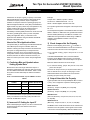
Ten Tips for Successful HSP50110/210EVAL
Board Operation
TM
Application Note
Listed below are ten tips to guide you quickly to successful
HSP50110/210EVAL board operation. While these tips do
not address complex problems, simple configuration
mistakes can keep the board from operating properly. The
HSP50110 Digital Quadrature Tuner (DQT) and HSP50210
Digital Costas Loop (DCL) demod chip set implement a very
capable, flexible PSK receiver. By reading this list of
solutions to common mistakes, you can proceed
immediately to obtaining BER performance of less than 1dB
from theory (0.5dB typical). When you have completed
reading this Application Note, you will want to read
Application Note AN9659: Using the HSP50110/210EVAL
Example Configuration Files.
How to Use This Application Note
It is important that you read through the HSP50110/210EVAL
User’s Manual prior using the evaluation board and
software. Following the setup instructions will minimize the
time spent on configuration/setup so that performance
evaluation can begin. Once you have entered your first
configuration and are ready to download that configuration to
the board, take time to read the list below and see if you
made one of the top ten most common setup/configuration
errors.
1) Confusing Bits and Symbols when
Setting Symbol Rate
Bit Rate is the rate of the single data stream input to a
modulator. Symbol Rate is the rate that I and Q are output
from the HSP50110/210EVAL Demodulator. Table 1 shows
the symbol to bit rate relationship for different modulation
formats.
May 1999
AN9715.1
Example:
Sample clock = 40MHz; Input RF = 70MHz.
Set the LO to 10MHz because 80 - 70 = 10;
2fS-RF = aliased digital IF desired in this case.
For input RF signals below the Nyquist of the sample clock,
RF = LO.
The example files supplied on the distribution disk use either
5MHz or 10MHz LO. 5MHz files were generated and tested
with the NCOM (HSP45116) as a 5MHz IF modulator. The
10MHz files were generated and tested using a 70MHz IF
modulator. (See AN9659 for details of the two test
configurations).
3) Clock Jumpers Not Set Properly
Determine if the sampling clock source, fS, is onboard or
external. The HSP50110/210EVAL can be sourced with an
external clock from the A/D or from test equipment.
a) For onboard clocking, jumper JP2 pins 29 to 31 and
30 to 32.
In the Data Path/Modulation menu, enter the Oscillator
Frequency as the Master Clock Frequency. The onboard
crystal oscillator is 40MHz. The clock is output on P1 pin 20.
Make sure that the A/D does not source this pin.
b) For external clocking, jumper JP2 pins 29 to 30, leave
pins 31 and 32 open.
The clock can be input on P1C pin 20 (sourced from A/D), or
from an external source, JP2 pin 30. See page 7 of the
HSP50110/210EVAL User’s Manual for clock inversion
jumpering (JP2 pins 25/26; pins 27/28).
NOTE: The HSP50110/210EVAL outputs SYMBOLS not BITS.
4) Output Select Not Set Properly
TABLE 1.
MODULATION
FORMAT
BIT RATE
SYMBOL (BAUD) RATE
BPSK
R
R
QPSK
R
R/2
8-PSK
R
R/3
16-PSK
R
R/4
Typical operation sets the Output Multiplexer Mux Control to
7 (0111). This configuration outputs the following signals:
ISOFT Decisions
(AOUT9-7): P2 pins C19 (MSB), A19, C18(LSB).
QSOFT Decisions
(AOUT6-4): P2 pins A18 (MSB), C17, A17(LSB).
The HSP50110/210EVAL outputs symbols, which enables a
variety of Forward Error Correcting (FEC) decoders to be
used with the DQT/DCL chip set.
IEND Decisions
(AOUT3-0; BOUT9-7): P2 pins C16, A16, A15, C14, A10,
C9, A9(LSB).
2) Incorrect LO Setting for Input IF
QEND Decisions
(BOUT6-0): P2 pins C8, A8, C7, A7, C6, C5, A5(LSB).
When undersampling the input IF, one has to remember that
the desired signal set in the software screen is the
downconverted IF.
1
The MSB's of the I and Q soft decisions can be used as hard
decisions for the I/Q symbols. These signals can be routed
to the bit error rate tester (BERT). IEND and QEND can be
1-888-INTERSIL or 321-724-7143
|
Intersil (and design) is a trademark of Intersil Americas Inc.
Copyright © Intersil Americas Inc. 2002. All Rights Reserved
Application Note 9715
sent to D/A convertors for displaying constellation and
transient responses on an oscilloscope.
5) Not Selecting SymbCLK as the
Data Clock
The DQT/DCL demod chip set outputs symbols. The clock
accompanying these symbols is SMBLCLK (PIN 70 of the
DCL) and GPOUT (P2-C21) of the EVAL board. JP5 pins
29-30 must be jumpered together.
The evaluation board clock CLKOUT on P2-C20 is a
reference clock derivative. DO NOT USE CLOCKOUT FOR
TYPICAL DATA OUTPUT.
The evaluation board clock CLKIN on P1-C20 is a reference
clock derivative/input. DO NOT USE CLKIN FOR TYPICAL
DATA OUTPUT.
The SLOCLK is brought to JP4-20 for use in outputting data
from the loop filters. DO NOT USE SLOCLK FOR DATA
OUTPUT (not used with DQT).
6) A/D Eval Board Not Properly Set
Identify the A/D board properly. Intersil offers a HI5702EV,
HI5702EV2, and an HI5703EV. Use the appropriate
alignment procedure for that board. Determine which input,
Video or RF, to use and jumper the board accordingly. The
fundamental difference is that Video assumes a single
ended input while RF is differential.
Either works fine for most of SATCOM Applications. The RF
input is needed for wideband high rate applications. If using
the RF input, verify that the RF transformer is installed. Intersil
does not supply transformers with all of the evaluation boards.
On all Intersil A/D Evaluation Boards, begin the setup by
aligning the reference voltages. This is usually accomplished
by adjusting several potentiometers. Follow the alignment
sequence recommended by the Evaluation Board User’s
Manuals, since one adjustment/alignment may actually
influence another.
Next align the clock reference to get 50% duty cycle using its
DC offset pot. Jumper for the evaluation boards for correct
Data Format. Jumper for the correct Clock polarity.
Application Notes AN9412 and AN9534 are supplied with
the converter evaluation boards and are instructive in the
alignment procedure.
7) Unused Input MSB Not Pulled High
Typical use of the DQT has a “real” signal as the input. A real
signal can be input on either the I or Q input pins. When
operating in the offset binary mode, pull MSB of the unused
input signal high to set the input bus to midscale.
2
The A/D Evaluation Boards that mate directly to the
HSP50110/210EVAL use the Q input pins for the RF input
signals, so pull IIN9 (the MSB) high.
Do not tie unused output bits to ground or VCC.
Do not tie input bits together if they are to be supplied by
different sources.
8) Input to A/D Not Set to a Proper Level
After complete alignment, the A/D input level should be less
than 1VPP input. Typically, the input level is 500mVPP.
Having an A/D input that is too low can degrade the
demodulator performance because insufficient bits are
available for processing.
The evaluation boards do not have an AGC circuit for setting
the optimal level into the A/D. The input level should be set
using total power (signal plus noise) for the maximum signal
density in the input band. Do not consider the signal alone.
Failure to do this may cause clipping of the A/D under these
full power conditions.
9) Modulator Configuration Does Not
Match Demod Configuration
This common error is related to Item #1 of this list. When setting
the modulator data input rate, know whether you are setting the
bit or symbol rate. On the Tx BERT it is usually bit rate.
On SATCOM modem equipment, it may be either bit rate or
symbol rate, so find out which it is.
One clue is whether the device has an integrated encoder. If
it does, than it can be assumed that the modulator is
adjusted by symbol rate. Remember that the symbol rate is
lower than the bit rate for higher order modulations of PSK.
10) Incorrect COM Port Selected
The primary symptom is that the computer is not talking to
the eval board. The typical cause of this error is having mistaken the identification of the PC serial port to which the
evaluation board cable is connected (COM1 or COM2).
Thus, the software is sending information to the wrong COM
port on the PC. The software menu will allow users to set the
COM port to 1 or 2. Be sure that the selected port is not
already allocated to some other device.
Application Note 9715
Other Common Problems
Data Path/Modulation, Menu Item 9.
The question is usually:
“What should I set the DQT output rate to, relative to the
baud rate (item 8)?”
• Typical operation sets this value to twice the baud
(symbol) rate. Set the DQT output rate to:
- 2 times the baud rate with the DCL RRC filters
- N times the baud rate with the DCL I&D filters,
where N is the number of samples integrated.
• With external FIR filters:
- Twice the baud rate, if not decimating
- Four times the baud rate, if decimating by 2
- Eight times the baud rate, if decimating by 4
Data Modulation = 0
There are the two characteristics of this setting:
1. No modulation expected on input (CW).
2. Output will be 1 on the I channel, 0 on the Q channel.
The NCOM As A Modulator
A common question when using an NCOM Evaluation Board
as a modulator, is how do I set the carrier frequency?
The answer is that you need to run both the NCOM and
DQT/DCL software packages on the same computer. One
will use the parallel port (DB25 connector) and the other will
use the serial (DB9) port.
External Filtering with an NCOM
Modulator
A common question is: “When using an NCOM Evaluation
Board as a modulator, do I need any external filters?”
“Amplifiers?”
It is always a good idea to employ a filter after the D/A
converter. A low pass filter will do just fine, but a bandpass
with sufficient bandwidth will also do.
The need for an amplifier is application specific. In general
you wish to set the signal output level high enough to
properly match the noise power to yield the SNR desired. A
filter is required when adding wideband noise to keep from
aliasing the out of band noise into the band of interest and
reducing the SNR.
Keep in mind that the NCOM allows programming of the
output signal amplitude in binary increments. This can be
helpful in finely setting the signal power. Do not use
amplitudes so low that the resolution of the output is
compromised, however.
D/A Considerations When Using the
NCOM Evaluation Board
The HI5721EV D/A Board can be readily used with the
NCOM Evaluation Board to generate an analog, modulated
IF. The HI5721 is a 10-bit, 125MHz D/A converter.
Application Note AN9410.1 is instructive in the proper use of
this converter.
Configure the NCOM first and then run the DEMODEVB
software for the demod chip set. It is always a good idea to
run NCOM_CHK to verify proper operation of the NCOM
Evaluation Board.
To set the carrier frequency of the NCOM, type the following
hexadecimal value into the “Center Frequency” window:
NCOM FC Parameter = [(Desired FC (Hz)/Sampling
frequency (Hz)) 232]HEX = [(FC/FXO) 232]HEX
NOTE: The evaluation boards can have a number of different
oscillators, so check the frequency of the one on your particular
board. Write the frequency, FXO , on the daughter board for
future reference. 40MHz is a common value for FXO , of the
onboard oscillator, for the HSPEVAL/HSP45116 and the
HSP50110/210EVAL.
BPSK data input is SB-24; QPSK data inputs are SB-24, 25.
Grounds are JB-24, 25. Set the PM select to zero.
All Intersil U.S. products are manufactured, assembled and tested utilizing ISO9000 quality systems.
Intersil Corporation’s quality certifications can be viewed at www.intersil.com/design/quality
Intersil products are sold by description only. Intersil Corporation reserves the right to make changes in circuit design, software and/or specifications at any time without
notice. Accordingly, the reader is cautioned to verify that data sheets are current before placing orders. Information furnished by Intersil is believed to be accurate and
reliable. However, no responsibility is assumed by Intersil or its subsidiaries for its use; nor for any infringements of patents or other rights of third parties which may result
from its use. No license is granted by implication or otherwise under any patent or patent rights of Intersil or its subsidiaries.
For information regarding Intersil Corporation and its products, see www.intersil.com
3