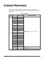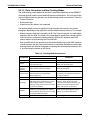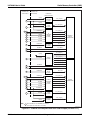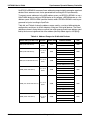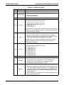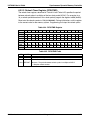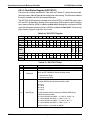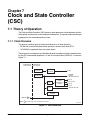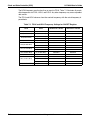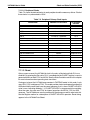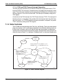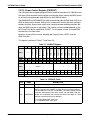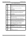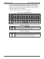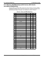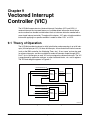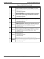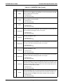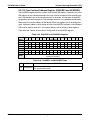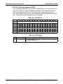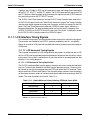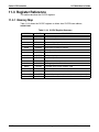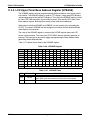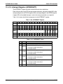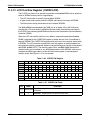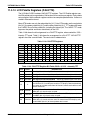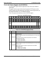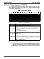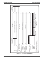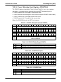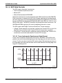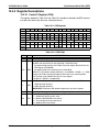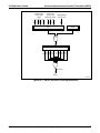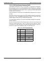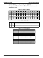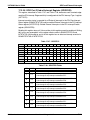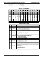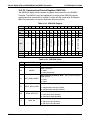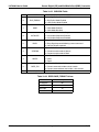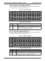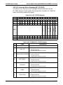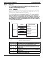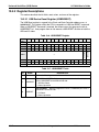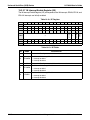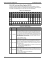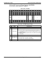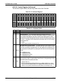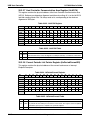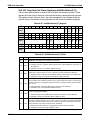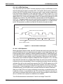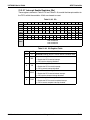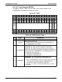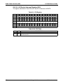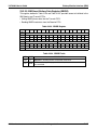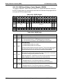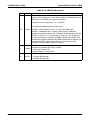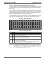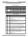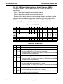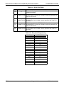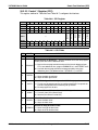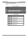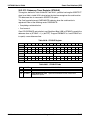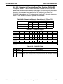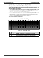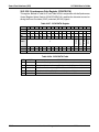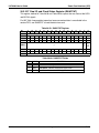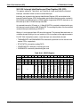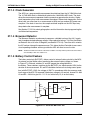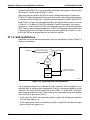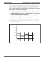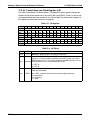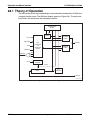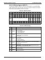
1
LH7A404
User’s Guide
2007 August 27
Content Revisions
This document contains the following changes to content, causing it to differ from
previous versions. Minor typographical changes, where they do not affect content, are not
tracked here.
Record of Revisions
DATE
5-17-04
PAGE
NO.
xl
Text
3-6
Text
6-6
Text
7-7 – 7-9
Text
8-2 – 8-4
Tables 8-1, 8-2, 8-3
8-7
Table 8-6
8-8
Tables 8-7, 8-8, and
text
12-8
Table 12-13
15-1
Text
15-3
Text
16-11
Text
17-6
Table 17-4
17-15
Tables 17-17, 17-18,
and text
17-16
Text, Table 17-20
19-14
Table 19-11
22-1
Text
23-1
Text
24-3
Text
24-6
Table 24-4
24-7
Table 24-7
25-1
Text
25-8
Table 25-13
26-2 – 26-5
26-8
Text
Table 26-64
28-7
Text
xxxix
SUMMARY OF CHANGES
References to pin numbers corrected within text
and register tables.
Text
26-45
Throughout
NXP Semiconductors
SECTION, TABLE,
OR ILLUSTRATION
Text, Tables, Figures
Bootwidth[1:0] changed to Width[1:0] for consistency
with LH7A400.
Text
Corrected package listing to 325 pin CABGA.
Ver. 1.3 — 27 August 2007
i
Content Revisions
LH7A404 User’s Guide
Record of Revisions (Cont’d)
DATE
PAGE
NO.
1-3
5-17-04
Table 1-1
SUMMARY OF CHANGES
INTBOOT, pin Y20 added.
Chapter 3
Text
Minor reorganization.
4-1
Text
‘Reset’ clarified to ‘rising edge of nPOR’.
4-4, 4-5
Text, Table 4-3
Clarified ‘logging’ during boot to ‘logged into the Boot
Status memory area’. Also added ‘Contents’ column to
Table 4-3.
9-2
Text, Table 9-1
Corrected to state that both VIC1 and VIC2 FIQ interrupts have equal priority.
9-9
Table 9-5
Bit 6, CODECIN description clarified.
9-40
Tables 9-49, 9-50,
and text
Description of ITOP2 register added.
11-4
Figure 11-3
LCDCLKIN added to Panel CLock Generation Block.
11-12
Figure 11-5
LCDCLKIN instead of 14.7456 MHz used label for input
to Clock Source Select.
11-23
Table 11-14
Bit 5, CSEL corrected from ‘Reserved’.
11-24
Table 11-15
Description of Bit 5, CSEL added.
18-5, 18-6
Text
MMC operation clarified.
18-15
Text
‘Busy Sequence’ corrected.
18-25, 18-26
Table 18-9
Definitions of the CLK_DIS, FIFO_FULL, and
FIFO_EMPTY bits corrected to reflect observed behavior.
18-27
Table 18-10
RATE register definitions and text corrected to reflect
observed behavior.
18-32
Text
Example added.
20-22
Text
Recommendation to add delay added.
20-28
Table 20-27
20-33
Table 20-37
20-37
Table 20-47
20-38
Table 20-49
20-39
Table 20-51
Book
All
2-4
Description corrected to reflect observed behavior.
Rolled revision from Preliminary to Version 1.0
Text
Highest priority interrupt corrected to Brownout.
5-19
Table 5-9
Made requirement to program RBLE to 1 for Writes
more explicit.
6-8
Section 6.1.3.3
Pin references deleted.
6-16, 6-29
Section 6.1.4.7,
Table 6-22
Clarified that programming the GBLCNFG:CKSD bit to 1
causes the SCKEx clock to free-run only when the
SDMC controls the EBI, and that it stops when the SMC
controls the EBI.
6-23
Section 6.1.6
Synchronous Flash section removed.
7-5
Table 7-2
Corrected divisors for the Timers.
11-20
Table 11-12
Removed “TIMING3” register from description; register
does not exist.
11-46
Figure 11-10
Replaced with correct figure.
11-48
Figure 11-12
Replaced with correct figure.
1-14-05
ii
SECTION, TABLE,
OR ILLUSTRATION
Ver. 1.3 — 27 August 2007
NXP Semiconductors
LH7A404 User’s Guide
Content Revisions
Record of Revisions (Cont’d)
DATE
PAGE
NO.
Corrected Port E to default to Output after reset.
18-22
Table 18-5
Corrected typographical errors.
18-34
Table 18-27,
Table 18-28
Reserved bits 3 and 4 (They do not function as interrupt
clear bits).
19-5
Numbered steps
Steps 1 and 3 corrected; 0 enables pull up; 1 disables
pull up.
19-14
Table 19-10
Corrrected DCP_CTRL from RO to RW.
20-19
Table 20-13
Corrected definition of the IR bit; description of 1 and 0
states reversed (bit should always be 0).
All
Corrected register name errors.
Table 23-26
Corrected definition of DIVFACT field.
Chapter 23
23-38
Corrected minor typographical errors; rolled revision
number to Version 1.1.
Throughout
4-5
Table 4-3
Corrected order of bits at address 0xB0013FFC.
Throughout
Corrected minor typos.
5-15
Section 5.1.7.3
Added section and illustration to clarify nWAIT; clarified
nPCWAIT description .
6-2
Text
Description of SDRAM memory banks corrected.
Table 7-1 &
Table 7-19
Corrected values for FCLK=132 MHz/HCLK=66 MHz
and FCLK=166 MHz/HCLK=83 MHz.
7-7
Section 7.1.2.1.1
and Section
7.1.2.1.2
Clarified that Standby and Halt will not be exited by the
TICK interrupt.
7-7
Section 7.1.2.2.1
Added “Because of ARM922T pipelining, five NOP instructions must follow this read.”
7-13
Table 7-8
Corrected example for PGMCLK bit.
8-3
Section 8.1.2
Corrected pin number reference for UART1.
8-7
Text
Added sentence that in 4-bit mono mode, Ports D and E
can be used for GPIO.
10-34
Table 10-34
Interrupt servicing information added to NFBINT.
10-35
Table 10-36
DONE definition corrected for 0 state; interrupt servicing
information added to NFB.
10-39
Table 10-40
10-41
Table 10-42
11-22
Table 11-16
Corrected STN behavior of VBP, VFP, VSW.
11-29
LCD Control Register (CONTROL)
Clarified how to change operating modes.
11-30
Table 11-27
Corrected definition of the WATERMARK bit.
11-41
Table 11-47
Corrected definition of the REVDEL field.
13-1
Text
Added statement that WDT inactive in STANDBY and
HALT Modes.
Chapter 4
7-4 &
7-19
3-30-06
NXP Semiconductors
SUMMARY OF CHANGES
Table 17-2,
Table 17-10 –
Table 17-13, text
17-2,
17-11 – 17-13
1-14-05
SECTION, TABLE,
OR ILLUSTRATION
Corrected size of register (32-bits).
Ver. 1.3 — 27 August 2007
iii
Content Revisions
LH7A404 User’s Guide
Record of Revisions (Cont’d)
DATE
PAGE
NO.
iv
SUMMARY OF CHANGES
13-2
Section 13.1.1.2
Added section.
13-7
Section 13.2.2.4
Corrected reset value of COUNT2 Register.
14-2
Text
Slight rewording of text.
Table 16-2 &
Table 16-12
Corrected divisor values for: 28800, 38400, 57600,
76800, 115200, 153600, and 230400.
16-13
Section 16.1.4.1
Corrected pin number references.
17-11
Table 17-10
Corrected ‘1’ state for Port E.
19-1, 19-2,
19-3
Figure 19-1,
Table 19-2,
Figure 19-2
Corrected EP0 FIFO size (16 Bytes) and
MAXP (16 Bytes).
19-12
Section 19.2.2
Corrected register name to USBDRESET.
19-11
Text
Minor rewording of text.
19-24
Table 19-33
Reworded definition of FIFO_NE bit.
19-30
Table 19-40
Added missing reset states for bits [3:2].
20-19
Table 20-13
Corrected BLE (bit 3) definition.
20-28
Table 20-33
Corrected definition of BCED field.
20-33
Table 20-47
Corrected order of bits: Bit 9 = NPS, Bit 8 = PSM.
20-36
Table 20-52
Corrected bit 31 to RW and reset to 0.
21-35
Table 21-53,
Table 21-54
Added inadvertently-omitted bit SLOT2TXCMP (bit 6) to
RIS register description.
23-27
Section 23.2.1
Corrected Base Address from 0x80000.0F00 to
0x8000.0F00
23-38
Table 23-25
Corrrected PEF and BRF bits to ‘RW’.
25-8
Table 25-12
Corrected table name to “SYNC2 Register”.
26-7
Section 26.1.5
Minor rewording.
27-2
Figure 27-1
27-4
Figure 27-2
27-12
Table 27-3
Minor correction to HW example.
27-17
Table 27-12
Minor rewording of NOC description.
16-9 &16-23
3-30-06
SECTION, TABLE,
OR ILLUSTRATION
References to AN5 removed.
27-19
Table 27-15
Corrected “...wait one A2DCLK periods” to “...wait two...”
27-23
Section 27.2.2.10
Corrected URL for Touch Screen Application Note.
Ver. 1.3 — 27 August 2007
NXP Semiconductors
LH7A404 User’s Guide
Content Revisions
Record of Revisions (Cont’d)
DATE
PAGE
NO.
SECTION, TABLE,
OR ILLUSTRATION
Corrected minor typographical errors; rolled revision
number to Version 1.2.
Throughout
5-19
Table 5-9
RBLE definition clarified.
5-20 - 5-21
Table 5-10 and
Figure 5-6
Added text, Table, and Figure to clarify use of IDCY bit.
6-16
Section 6.1.4.7
Corrected description of clock shutdown description.
6-29
Table 6-22
Corrected description of the CKSD bit.
Table 7-1, Table 719
Added value for 266/133 MHz operation.
7-11
Table 7-6
Corrected values for CHIPID field.
7-17
Section 7.2.2.5
Corrected time in Standby state to “2 to 4 32-kHz clock
periods.”
19-13
Section 19.2.2.2
Clarified the description of this register.
19-14
Table 19-11
Definition of the UC_RESUME bit corrected to “USB Device generates RESUME signalling in SUSPEND mode
when this bit is 1.”
19-20
Table 19-23
SUSINTEN definition corrected; “This bit also enables
and disables the RESUME interrupt.” removed.
19-23
Section 19.2.3.2
EP0 maximum packet size corrected to 16 bits.
23-19
Figure 23-12
Figure corrected.
23-18
Section 23.1.2.5.6
Text corrected to explain that PEC must be calculated
by software and provides the formula.
Table 23-4,
Table 23-32,
Table 23-34
Clarified condition that asserts the MTCI interrupt.
7-4, 7-19
6-15-07
23-26, 23-43,
23-46
8-27-07
NXP Semiconductors
SUMMARY OF CHANGES
All
—
All references to Sharp replaced with NXP. Revision
number rolled to Version 1.3.
Ver. 1.3 — 27 August 2007
v
Content Revisions
vi
LH7A404 User’s Guide
Ver. 1.3 — 27 August 2007
NXP Semiconductors
Table of Contents
Preface
Conventions and Terms ..........................................................................................xli
Unconnected (Floating) Inputs ............................................................................xli
Multiplexed Pins ..................................................................................................xli
Pin Names .......................................................................................................... xlii
Peripheral Devices ............................................................................................. xlii
Register Addresses ............................................................................................ xlii
Register Tables ................................................................................................. xliii
Chapter 1 – Introduction
1.1 Description ....................................................................................................... 1-1
1.2 Power Supply Sequencing ............................................................................... 1-2
1.3 Functional Pin List ............................................................................................ 1-2
Chapter 2 – System Overview
2.1 Introduction....................................................................................................... 2-1
2.2 Features ........................................................................................................... 2-1
2.3 Block Diagram .................................................................................................. 2-3
2.4 Power Supply Sequencing ............................................................................... 2-4
Chapter 3 – Core and Data Paths
3.1 Theory of Operation ......................................................................................... 3-1
3.1.1 Operating States ....................................................................................... 3-2
3.1.2 Instruction and Data Cache ....................................................................... 3-3
3.1.3 Memory Management Unit ........................................................................ 3-4
3.1.4 Internal and External Memory ................................................................... 3-4
3.1.4.1 Memory Map....................................................................................... 3-5
3.1.5 Boot Modes ............................................................................................... 3-6
3.1.5.1 Internal Boot ROM.............................................................................. 3-6
3.2 Buses ............................................................................................................... 3-7
3.2.1 Advanced High-Performance Bus (AHB) .................................................. 3-7
3.2.1.1 Arbitration ........................................................................................... 3-7
3.2.1.2 Clock Generation and Bus Clocking Modes ..................................... 3-11
3.2.1.3 Standard Bus Clocking Modes ......................................................... 3-12
3.2.1.4 Fastbus Extension Bus Clocking Mode ............................................ 3-13
3.2.2 Advanced Peripheral Bus (APB) ............................................................. 3-14
3.2.3 The AHB-to-APB Bridge .......................................................................... 3-15
3.3 The DMA Controller........................................................................................ 3-15
NXP Semiconductors
Ver. 1.3 — 27 August 2007
iii
Table of Contents
LH7A404 User’s Guide
Chapter 4 – Boot ROM
4.1 Theory of Operation ......................................................................................... 4-1
4.1.1 Compatible External Boot Devices ............................................................ 4-1
4.1.2 Boot Device Selection ............................................................................... 4-1
4.1.3 Booting From NAND Flash ........................................................................ 4-3
4.1.4 Booting From an I2C Device ..................................................................... 4-4
4.1.5 Booting From UART2 Using XMODEM..................................................... 4-4
4.1.6 Logging and Error Handling ...................................................................... 4-5
4.2 Register Reference .......................................................................................... 4-6
4.2.1 Memory Map ............................................................................................. 4-6
4.2.2 Register Descriptions ................................................................................ 4-6
4.2.2.1 Boot ROM Clear Register (BOOTCLR) .............................................. 4-6
Chapter 5 – Static Memory Controller (SMC)
5.1 Theory of Operation ......................................................................................... 5-1
5.1.1 Operation Overview................................................................................... 5-2
5.1.1.1 Configuring the Multiplexed Pins ........................................................ 5-2
5.1.1.2 Using External Memory ...................................................................... 5-3
5.1.2 Using PCMCIA and CompactFlash ........................................................... 5-3
5.1.3 Pin Multiplexing ......................................................................................... 5-4
5.1.3.1 Non-SMC Systems ............................................................................. 5-5
5.1.3.2 General Purpose I/O and SMC PC Card Multiplexing........................ 5-5
5.1.4 Memory Bank Selection ............................................................................ 5-9
5.1.4.1 PC Card Address Space .................................................................. 5-10
5.1.5 Byte Lane Write Control .......................................................................... 5-11
5.1.6 Access Sequencing ................................................................................. 5-13
5.1.7 Wait State Generation ............................................................................. 5-13
5.1.7.1 Memory Bank Timing........................................................................ 5-13
5.1.7.2 PC Card Timing ................................................................................ 5-14
5.1.7.3 nWAIT Signalling .............................................................................. 5-15
5.1.8 Write Protection....................................................................................... 5-16
5.1.9 External Bus Interface ............................................................................. 5-16
5.2 Register Reference ........................................................................................ 5-17
5.2.1 Memory Map ........................................................................................... 5-17
5.2.2 Register Descriptions .............................................................................. 5-18
5.2.2.1 Bank Configuration Registers (BCRx) .............................................. 5-18
5.2.2.2 PC Card Attribute Space Registers (PCxATTRIB) ........................... 5-20
5.2.2.3 PC Card Common Memory Space Registers (PCxCOM) ................ 5-21
5.2.2.4 PC Card I/O Space Registers (PCxIO)............................................. 5-22
5.2.2.5 PCMCIA Control Register (PCMCIACON) ....................................... 5-23
iv
Ver. 1.3 — 27 August 2007
NXP Semiconductors
LH7A404 User’s Guide
Table of Contents
Chapter 6 – Synchronous Dynamic Memory Controller
6.1 Theory of Operation ......................................................................................... 6-1
6.1.1 Memory Banks .......................................................................................... 6-2
6.1.2 Operational Overview ................................................................................ 6-3
6.1.2.1 SDMC Operation ................................................................................ 6-3
6.1.2.2 Designing an SDRAM System............................................................ 6-4
6.1.2.3 Read and Write Operation.................................................................. 6-4
6.1.2.4 Other Functions .................................................................................. 6-5
6.1.3 External Hardware System Design ........................................................... 6-5
6.1.3.1 Control Signals ................................................................................... 6-5
6.1.3.2 Pin Multiplexing .................................................................................. 6-6
6.1.3.3 Chip Select Decoding ......................................................................... 6-8
6.1.3.4 Address, Data, and Control Requirements......................................... 6-8
6.1.4 Programming the SDMC ......................................................................... 6-14
6.1.4.1 Determining Parameter Values ........................................................ 6-14
6.1.4.2 Auto Precharge................................................................................. 6-14
6.1.4.3 RAS to CAS Latency ........................................................................ 6-15
6.1.4.4 CAS Latency..................................................................................... 6-15
6.1.4.5 External Bus Width ........................................................................... 6-15
6.1.4.6 Burst Length ..................................................................................... 6-15
6.1.4.7 Clock Enable and Clock Shutdown .................................................. 6-16
6.1.4.8 Configuring the SDRAM device Load Mode Register ...................... 6-16
6.1.4.9 Configuring the Refresh Timer Register ........................................... 6-20
6.1.5 Initializing the SDRAM Devices ............................................................... 6-21
6.1.5.1 Initialization When Debugging .......................................................... 6-21
6.1.5.2 General Initialization Sequence........................................................ 6-21
6.1.5.3 JEDEC General SDRAM Initialization Sequence ............................. 6-22
6.1.5.4 Micron SDRAM Initialization Sequence............................................ 6-22
6.1.6 Self Refresh............................................................................................. 6-23
6.2 Boot Modes .................................................................................................... 6-23
6.2.1 Synchronous Memory Boot Interrupt Behavior ....................................... 6-24
6.3 Register Reference ........................................................................................ 6-25
6.3.1 Memory Map ........................................................................................... 6-25
6.3.2 Register Descriptions .............................................................................. 6-26
6.3.2.1 Synchronous Domain Chip Select Configuration
Registers (SDCSC) .................................................................................. 6-26
6.3.2.2 SDRAM Global Configuration Register (GBLCNFG)........................ 6-29
6.3.2.3 Refresh Timer Register (RFSHTMR) ............................................... 6-31
6.3.2.4 Boot Status Register (BOOTSTAT).................................................. 6-32
NXP Semiconductors
Ver. 1.3 — 27 August 2007
v
Table of Contents
LH7A404 User’s Guide
Chapter 7 – Clock and State Controller (CSC)
7.1 Theory of Operation ......................................................................................... 7-1
7.1.1 Clock Domains .......................................................................................... 7-1
7.1.1.1 32.768 kHz Clock ............................................................................... 7-2
7.1.1.2 14.7456 MHz Clock ............................................................................ 7-2
7.1.1.3 Reset .................................................................................................. 7-5
7.1.1.4 TICK and TICK Timeout Interrupt Generation .................................... 7-6
7.1.2 State Controller ......................................................................................... 7-6
7.1.2.1 Run State............................................................................................ 7-7
7.1.2.2 Halt State............................................................................................ 7-7
7.1.2.3 Standby State ..................................................................................... 7-8
7.2 Register Reference ........................................................................................ 7-10
7.2.1 Memory Map ........................................................................................... 7-10
7.2.2 Register Descriptions .............................................................................. 7-11
7.2.2.1 Power Reset Register (PWRSR)...................................................... 7-11
7.2.2.2 Power Control Register (PWRCNT) ................................................. 7-13
7.2.2.3 Halt and Standby Read-to-Enter Registers (HALT) (STBY)............. 7-15
7.2.2.4 Interrupt and Flag Clearing Registers
(BLEOI, MCEOI, TEOI, STFCLR) ............................................................ 7-16
7.2.2.5 Clock Set Register (CLKSET) .......................................................... 7-17
7.2.2.6 General Purpose Storage Registers (SCRREGx) ............................ 7-20
7.2.2.7 USB Device Reset Register (USBDRESET) .................................... 7-21
7.2.2.8 Bus Master Arbitration Register (BMAR).......................................... 7-22
7.2.2.9 Boot ROM Clear Register (BOOTCLR) ............................................ 7-23
Chapter 8 – Pin and Signal Multiplexing
8.1 Theory of Operation ......................................................................................... 8-1
8.1.1 External Interrupt and GPIO Port F Multiplexing ....................................... 8-2
8.1.2 UART and GPIO Port B and Port C Multiplexing ...................................... 8-3
8.1.3 Memory, MultiMediaCard, GPIO Port G, GPIO Port H,
and Address Multiplexing ............................................................................... 8-4
8.1.3.1 PCMCIA/Compact Flash Multiplexing ................................................ 8-5
8.1.3.2 Synchronous and Asynchronous Memory Controller External Address
Bus Multiplexing ......................................................................................... 8-5
8.1.4 LCD and GPIO Multiplexing ...................................................................... 8-6
8.1.4.1 Reset State......................................................................................... 8-7
8.1.5 AC97, ACI, and GPIO Multiplexing ........................................................... 8-7
8.1.6 Smart Card Interface, GPIO, and Address Multiplexing ............................ 8-8
8.1.7 Battery Monitor Interface and GPIO Multiplexing ...................................... 8-8
vi
Ver. 1.3 — 27 August 2007
NXP Semiconductors
LH7A404 User’s Guide
Table of Contents
Chapter 9 – Vectored Interrupt Controller (VIC)
9.1 Theory of Operation ......................................................................................... 9-1
9.1.1 Interrupt Priority ......................................................................................... 9-2
9.1.2 Interrupt Assignment ................................................................................. 9-3
9.2 Register Reference .......................................................................................... 9-5
9.2.1 Memory Map ............................................................................................. 9-5
9.2.2 Register Descriptions ................................................................................ 9-7
9.2.2.1 IRQ Status Register (IRQSTATUS1 and IRQSTATUS2) ................... 9-7
9.2.2.2 FIQ Status Register (FIQSTATUS1 and FIQSTATUS2) .................. 9-13
9.2.2.3 Raw Interrupt Status Register (RAWINTR1 and RAWINTR2) ......... 9-19
9.2.2.4 Interrupt Select Register (INTSEL1 and INTSEL2) .......................... 9-25
9.2.2.5 Interrupt Enable Register (INTEN1 and INTEN2)............................. 9-26
9.2.2.6 Interrupt Enable Clear Register (INTENCLR1 and INTENCLR2)..... 9-27
9.2.2.7 Software Interrupt Register (SOFTINT1 and SOFTINT2) ................ 9-28
9.2.2.8 Software Interrupt Clear Register (SOFTINTCLR1 and SOFTINTCLR2)
9-29
9.2.2.9 Vector Address Register (VECTADDR1 and VECTADDR2)............ 9-30
9.2.2.10 Non-Vectored Address Register (NVADDR1 and NVADDR2) ....... 9-31
9.2.2.11 Vector Address Registers (VAD1[15:0] and VAD2[15:0])............... 9-32
9.2.2.12 Vector Control Registers (VECTCNTL1[15:0] and VECTCNTL2[15:0])
9-34
9.2.2.13 Test Control Register (ITCR1 and ITCR2) ..................................... 9-36
9.2.2.14 Test Input Register (ITIP1) ............................................................. 9-37
9.2.2.15 Test Input Register (ITIP2) ............................................................. 9-38
9.2.2.16 Test Output Register (ITOP1)......................................................... 9-39
9.2.2.17 Test Output Register ITOP2 ........................................................... 9-40
Chapter 10 – Direct Memory Access (DMA) Controller
10.1 Theory of Operation ..................................................................................... 10-1
10.1.1 DMA External Interface Signals ............................................................ 10-2
10.1.1.1 Interrupt Interface ........................................................................... 10-5
10.1.1.2 Internal M2P/P2M Data Unpacker/Packer Description................... 10-5
10.1.2 M2M DMA Functional Description ......................................................... 10-6
10.1.2.1 Data Transfer Initiation ................................................................... 10-6
10.1.2.2 Data Transfer Termination.............................................................. 10-7
10.1.2.3 Memory Block Transfer .................................................................. 10-8
10.1.2.4 Bandwidth Control .......................................................................... 10-8
10.1.2.5 External Peripheral DMA Request (DREQ) Mode.......................... 10-8
10.1.3 DMA Data Transfer Size Determination ................................................ 10-9
10.1.3.1 Internal Peripheral and Software Initiated M2M Transfers ............. 10-9
10.1.3.2 External M2P/P2M Transfers ....................................................... 10-10
10.1.4 Buffer Descriptors................................................................................ 10-10
10.1.4.1 Internal M2P/P2M Channel RX Buffer.......................................... 10-10
10.1.4.2 Internal M2P/P2M Channel TX Buffer .......................................... 10-10
10.2 Memory Map .............................................................................................. 10-13
10.2.1 Global DMA Register Map................................................................... 10-14
10.2.1.1 Global Channel Arbitration Register (GCA).................................. 10-14
10.2.1.2 Global Interrupt Register (GIR)..................................................... 10-15
NXP Semiconductors
Ver. 1.3 — 27 August 2007
vii
Table of Contents
LH7A404 User’s Guide
10.2.2 Memory-to-Peripheral/Peripheral-to-Memory
Channel Register Map................................................................................ 10-17
10.2.2.1 Control Register (PCONTROL) .................................................... 10-18
10.2.2.2 Interrupt Status Register (PINTERRUPT) .................................... 10-20
10.2.2.3 Peripheral Port Allocation Register (PPALLOC)........................... 10-21
10.2.2.4 Channel Status Register (PSTATUS)........................................... 10-23
10.2.2.5 Bytes Remaining Register (REMAIN)........................................... 10-25
10.2.2.6 Maximum Buffer Count Register (MAXCNT0 and MAXCNT1)..... 10-26
10.2.2.7 Base Address Registers (BASE0 and BASE1) ............................ 10-27
10.2.2.8 Current Address Registers (CURRENT0 and CURRENT1)......... 10-28
10.2.3 Memory-to-Memory Channel Register Map ........................................ 10-29
10.2.3.1 Control Register (MCONTROL).................................................... 10-30
10.2.3.2 Interrupt Status Register (MINTERRUPT).................................... 10-34
10.2.3.3 Channel Status Register (MSTATUS) .......................................... 10-35
10.2.3.4 Byte Count Remaining Registers (BCRx)..................................... 10-38
10.2.3.5 Source Address Base Registers (SAR_BASEx) .......................... 10-39
10.2.3.6 Current Source Address Base Registers (SAR_CURRENTx) ..... 10-40
10.2.3.7 Destination Address Base Registers (DAR_BASEx).................... 10-41
10.2.3.8 Current Destination Address Base Register (DAR_CURRENTx) 10-42
Chapter 11 – Color LCD Controller
11.1 Introduction................................................................................................... 11-1
11.1.1 LCD Panel Architecture ......................................................................... 11-2
11.1.2 Features ................................................................................................ 11-3
11.1.3 Theory of Operation .............................................................................. 11-3
11.1.3.1 Memory Management Unit ............................................................. 11-5
11.1.3.2 Dual-panel Color STN Operation.................................................... 11-6
11.1.3.3 Dual-panel Monochrome STN Operation ....................................... 11-6
11.1.3.4 Single-panel Color STN Operation ................................................. 11-7
11.1.3.5 Single-panel Monochrome STN Operation..................................... 11-7
11.1.3.6 TFT Operation ................................................................................ 11-7
11.1.3.7 Storing Pixels in the Frame Buffer.................................................. 11-8
11.1.3.8 Pixel Serializer................................................................................ 11-8
11.1.3.9 How Pixels are Stored in Memory .................................................. 11-8
11.1.4 LCD Panel Resolution ......................................................................... 11-10
11.1.4.1 Color and Gray Scale Selection ................................................... 11-10
11.1.5 LCD Data Multiplexing......................................................................... 11-12
11.1.6 CLCDC Clock Generation ................................................................... 11-13
11.1.7 LCD Interface Timing Signals.............................................................. 11-14
11.1.7.1 LCD Horizontal Timing Signals..................................................... 11-14
11.1.7.2 LCD Vertical Timing Signals......................................................... 11-15
11.1.8 LCD Power Sequencing at Turn-On and Turn-Off .............................. 11-15
11.1.8.1 Minimizing a Retained Image on the LCD .................................... 11-15
11.1.9 CLCDC Interrupts ................................................................................ 11-16
11.1.9.1 Master Bus Error Interrupt — MBEI.............................................. 11-17
11.1.9.2 Vertical Compare Interrupt — CVCI ............................................. 11-17
11.1.9.3 LCD Next Base Address Update Interrupt — BUI ........................ 11-17
11.1.9.4 LCD FIFO Underflow Interrupt — FUI .......................................... 11-17
viii
Ver. 1.3 — 27 August 2007
NXP Semiconductors
LH7A404 User’s Guide
Table of Contents
11.2 Advanced LCD Interface ............................................................................ 11-18
11.2.1 Theory of Operation ............................................................................ 11-18
11.2.1.1 Bypass Mode................................................................................ 11-19
11.2.1.2 Active Mode.................................................................................. 11-19
11.2.1.3 CLCDC Setup for AD-TFT or HR-TFT Operation......................... 11-19
11.3 Register Reference .................................................................................... 11-20
11.3.1 Memory Map ....................................................................................... 11-20
11.3.2 CLCDC Register Descriptions ............................................................. 11-21
11.3.2.1 LCD Timing 0 Register (TIMING0) ............................................... 11-21
11.3.3 LCD Timing 1 Register (TIMING1) ...................................................... 11-22
11.3.4 LCD Timing 2 Register (TIMING2) ...................................................... 11-24
11.3.5 LCD Upper Panel Base Address Register (UPBASE) ........................ 11-26
11.3.6 LCD Lower Panel Base Address Register (LPBASE) ......................... 11-27
11.3.7 LCD Interrupt Enable Register (INTREN) ........................................... 11-28
11.3.8 LCD Control Register (CONTROL) ..................................................... 11-29
11.3.9 Interrupt Status Register (STATUS) .................................................... 11-32
11.3.10 Interrupt Register (INTERRUPT)....................................................... 11-33
11.3.11 LCD Upper Panel Current Address Register (UPCUR)..................... 11-34
11.3.12 LCD Lower Panel Current Address Register (LPCUR) ..................... 11-35
11.3.13 LCD Overflow Register (OVERFLOW).............................................. 11-36
11.3.14 LCD Palette Registers (PALETTE) ................................................... 11-37
11.4 ALI Register Reference .............................................................................. 11-38
11.4.1 ALI Memory Map ................................................................................. 11-38
11.4.2 ALI Register Descriptions .................................................................... 11-38
11.4.3 ALI Setup Register (ALISETUP) ......................................................... 11-39
11.4.4 ALI Control Register (ALICONTROL).................................................. 11-40
11.4.5 ALI Timing 1 Register (ALITIMING1) .................................................. 11-41
11.4.6 ALI Timing 2 Register (ALITIMING2) .................................................. 11-42
11.5 Color LCD System Timing Waveforms....................................................... 11-43
11.5.1 STN Horizontal Timing ........................................................................ 11-43
11.5.2 TFT Horizontal Timing ......................................................................... 11-43
11.5.3 TFT Vertical Timing ............................................................................. 11-43
11.5.4 AD-TFT and HR-TFT Horizontal Timing Waveforms........................... 11-48
11.5.5 AD-TFT and HR-TFT Vertical Timing .................................................. 11-49
Chapter 12 – Timers
12.1 Theory of Operation ..................................................................................... 12-1
12.2 Register Reference ...................................................................................... 12-2
12.2.1 Memory Map ......................................................................................... 12-2
12.2.2 Register Descriptions ............................................................................ 12-3
12.2.2.1 Timer Load Registers (LOADx) ...................................................... 12-3
12.2.2.2 Timer Value Registers (VALUEx) ................................................... 12-4
12.2.2.3 Timer End-of-Interrupt Registers (TCEOIx).................................... 12-5
12.2.2.4 Timer Control Registers (CONTROLx)........................................... 12-6
12.2.2.5 Timer Buzzer Count Register (BZCON) ......................................... 12-8
NXP Semiconductors
Ver. 1.3 — 27 August 2007
ix
Table of Contents
LH7A404 User’s Guide
Chapter 13 – Watchdog Timer (WDT)
13.1 Theory of Operation ..................................................................................... 13-1
13.1.1 WDT Configuration ................................................................................ 13-1
13.1.1.1 Interrupt Generation ....................................................................... 13-2
13.1.1.2 Initialization Following Reset .......................................................... 13-2
13.2 Register Reference ...................................................................................... 13-3
13.2.1 Memory Map ......................................................................................... 13-3
13.2.2 Register Descriptions ............................................................................ 13-4
13.2.2.1 Control Register (CTL) ................................................................... 13-4
13.2.2.2 Counter Reset Register (RST) ....................................................... 13-5
13.2.2.3 Status Register (STATUS) ............................................................. 13-6
13.2.2.4 Current Watchdog Count Registers (COUNT[3:0]) ........................ 13-7
Chapter 14 – Real Time Clock (RTC)
14.1 Theory of Operation ..................................................................................... 14-1
14.1.1 RTC Interrupt......................................................................................... 14-1
14.1.2 Configuring the RTC for Use ................................................................. 14-1
14.2 Register Reference ...................................................................................... 14-2
14.2.1 Memory Map ......................................................................................... 14-2
14.2.2 Register Descriptions ............................................................................ 14-3
14.2.2.1 RTC Data Register (RTCDR) ......................................................... 14-3
14.2.2.2 RTC Load Register (RTCLR) ......................................................... 14-4
14.2.2.3 RTC Match Register (RTCMR)....................................................... 14-5
14.2.2.4 RTC Interrupt Status and Interrupt Clear Register
(RTCSTAT and RTCEOI) ......................................................................... 14-6
14.2.2.5 RTC Control Register (RTCCR) ..................................................... 14-8
Chapter 15 – Synchronous Serial Port (SSP)
15.1 Theory of Operation ..................................................................................... 15-1
15.1.1 Clocking................................................................................................. 15-1
15.1.2 FIFOs .................................................................................................... 15-1
15.1.3 Interrupts ............................................................................................... 15-2
15.1.4 SSP Data Formats ................................................................................ 15-3
15.1.4.1 Texas Instruments Synchronous Serial Format ............................. 15-3
15.1.4.2 Motorola SPI Format ...................................................................... 15-4
15.1.4.3 National Semiconductor MICROWIRE Format............................... 15-7
15.2 Register Reference ...................................................................................... 15-8
15.2.1 Memory Map ......................................................................................... 15-8
15.2.2 Register Descriptions ............................................................................ 15-9
15.2.2.1 Control 0 Register (CR0) ................................................................ 15-9
15.2.2.2 Control 1 Register (CR1) .............................................................. 15-11
15.2.2.3 Interrupt Identification Register (IIR)............................................. 15-13
15.2.2.4 Receive Overrun End-of-Interrupt Register (RXEOI) ................... 15-14
15.2.2.5 Data Register (DR) ....................................................................... 15-15
15.2.2.6 Clock Prescale Register (CPR) .................................................... 15-16
15.2.2.7 SSP Status Register (SR) ............................................................ 15-17
x
Ver. 1.3 — 27 August 2007
NXP Semiconductors
LH7A404 User’s Guide
Table of Contents
Chapter 16 – Universal Asynchronous Receiver/Transmitter (UART)
16.1 Theory of Operation ..................................................................................... 16-1
16.1.1 UART Overview..................................................................................... 16-1
16.1.1.1 Data Protocol.................................................................................. 16-5
16.1.1.2 Operation Summary ....................................................................... 16-6
16.1.2 Configuring the UARTs ......................................................................... 16-8
16.1.2.1 Selecting FIFO or Non-FIFO Operation.......................................... 16-8
16.1.2.2 Specifying the Data Size ................................................................ 16-8
16.1.2.3 Enabling and Specifying Parity....................................................... 16-8
16.1.2.4 Specifying the Baud Rate ............................................................... 16-8
16.1.2.5 Setting Low Power Mode for Infrared Operation .......................... 16-10
16.1.2.6 Selecting Signal Polarity............................................................... 16-10
16.1.2.7 Configuring the UART3 Multiplexed Pins ..................................... 16-10
16.1.2.8 Configuring UART1 for Infrared Operation ................................... 16-10
16.1.3 Managing the Receive Operation ........................................................ 16-10
16.1.3.1 UART Input Pins........................................................................... 16-11
16.1.3.2 Framing ........................................................................................ 16-11
16.1.3.3 Data Handling............................................................................... 16-11
16.1.3.4 Checking Parity ............................................................................ 16-12
16.1.3.5 Identifying a Break........................................................................ 16-12
16.1.4 Managing the Transmit Operation ....................................................... 16-13
16.1.4.1 Configuring the Output Pins ......................................................... 16-13
16.1.4.2 Framing and Generating Parity .................................................... 16-13
16.1.4.3 Entering a Break State ................................................................. 16-13
16.1.4.4 Handling the Data......................................................................... 16-13
16.1.5 Using the External Modem Control Signals......................................... 16-14
16.1.6 Configuring and Handling Interrupts.................................................... 16-15
16.1.7 Configuring Loopback Mode ............................................................... 16-18
16.2 Register Reference .................................................................................... 16-19
16.2.1 Memory Map ....................................................................................... 16-19
16.2.2 Register Descriptions .......................................................................... 16-20
16.2.2.1 Data Register (DATA)................................................................... 16-20
16.2.2.2 FIFO and Framing Control Register (FCON)................................ 16-22
16.2.2.3 Baud Rate Control Register (BRCON) ......................................... 16-23
16.2.2.4 Control Register (CONx) .............................................................. 16-24
16.2.2.5 Status Register (STATUS) ........................................................... 16-26
16.2.2.6 Raw Interrupt Register (RAWISR)................................................ 16-27
16.2.2.7 Interrupt Enable Register (INTEN) ............................................... 16-29
16.2.2.8 Masked Interrupt Status Register (MISR)..................................... 16-30
16.2.2.9 Read Error Status and Clear Register (RES) ............................... 16-31
16.2.2.10 Error Interrupt Clear Register (EIC)............................................ 16-32
16.2.2.11 DMA Control Register (DMACR) ................................................ 16-33
NXP Semiconductors
Ver. 1.3 — 27 August 2007
xi
Table of Contents
LH7A404 User’s Guide
Chapter 17 – GPIO and External Interrupts
17.1 Theory of Operation ..................................................................................... 17-1
17.1.1 GPIO Nomenclature .............................................................................. 17-1
17.1.2 GPIO Port Usage .................................................................................. 17-2
17.1.2.1 Programming GPIO Pins ................................................................ 17-2
17.1.2.2 Input/Output Data ........................................................................... 17-2
17.1.3 Port F External Interrupts ...................................................................... 17-3
17.1.3.1 Configuring the Interrupts ............................................................... 17-4
17.1.3.2 Enabling and Clearing Interrupts .................................................... 17-6
17.2 Register Reference ...................................................................................... 17-7
17.2.1 Memory Map ......................................................................................... 17-7
17.2.2 Register Descriptions ............................................................................ 17-9
17.2.2.1 GPIO Data Registers (PyD)............................................................ 17-9
17.2.2.2 GPIO Pin Data Registers (PyPD) ................................................. 17-10
17.2.2.3 GPIO Data Direction Registers (PyDD)........................................ 17-11
17.2.2.4 GPIO Keyboard Control Register (KBDCTL)................................ 17-15
17.2.2.5 GPIO Pin Multiplexing Register (PINMUX)................................... 17-16
17.2.2.6 Interrupt Type 1 Register (INTTYPE1) ......................................... 17-18
17.2.2.7 Interrupt Type 2 Register (INTTYPE2) ......................................... 17-20
17.2.2.8 GPIO Port F End-of-Interrupt Register (GPIOFEOI) .................... 17-21
17.2.2.9 GPIO Port F Interrupt Enable Register (GPIOINTEN).................. 17-22
17.2.2.10 GPIO Port F Interrupt Status Register (INTSTATUS) ................ 17-23
17.2.2.11 GPIO Port F Raw Interrupt Status Register (RAWINSTATUS) .. 17-24
17.2.2.12 GPIO Port F Debounce Register (GPIODB)............................... 17-25
Chapter 18 – Secure Digital (SD) and MultiMediaCard (MMC) Controller
18.1 Theory of Operation ..................................................................................... 18-1
18.1.1 Interface ................................................................................................ 18-2
18.1.1.1 SD/MMC Card Registers ................................................................ 18-2
18.1.2 SD/MMC Memory Organization ............................................................ 18-3
18.1.3 Reset ..................................................................................................... 18-4
18.1.4 Clock Generation and Control ............................................................... 18-4
18.1.5 DMA Operation...................................................................................... 18-5
18.1.6 SD/MMC Card Communication Overview ............................................. 18-6
18.1.6.1 Identification Mode ......................................................................... 18-6
18.1.6.2 Data Transfer Mode........................................................................ 18-7
18.1.7 Command Operation and Protocols .................................................... 18-10
18.1.7.1 Basic, No Data, Command-Response Sequence ........................ 18-10
18.1.7.2 Data Transfer................................................................................ 18-11
18.1.7.3 Busy Sequence ............................................................................ 18-14
18.1.8 Error Detection .................................................................................... 18-15
18.1.9 Interrupts ............................................................................................. 18-15
18.1.10 Transaction Examples ....................................................................... 18-16
18.1.10.1 Initialize....................................................................................... 18-16
18.1.10.2 No Data Command and Response Transaction......................... 18-17
18.1.10.3 Erase .......................................................................................... 18-17
18.1.10.4 Single Block Write ...................................................................... 18-17
18.1.10.5 Single Block Read ...................................................................... 18-18
xii
Ver. 1.3 — 27 August 2007
NXP Semiconductors
LH7A404 User’s Guide
Table of Contents
18.1.10.6 Multiple Block Write .................................................................... 18-19
18.1.10.7 Multiple Block Read.................................................................... 18-20
18.1.10.8 Stream Write............................................................................... 18-20
18.1.10.9 Stream Read .............................................................................. 18-21
18.2 Register Reference .................................................................................... 18-22
18.2.1 Memory Map ....................................................................................... 18-22
18.2.2 Register Descriptions .......................................................................... 18-23
18.2.2.1 Clock Control Register (CLKC)..................................................... 18-23
18.2.2.2 Status Register (STATUS) ........................................................... 18-24
18.2.2.3 Clock Rate Divisor Register (RATE)............................................. 18-26
18.2.2.4 Clock Predivide Register (PREDIV) ............................................. 18-27
18.2.2.5 Command and Control Register (CMDCON) ............................... 18-28
18.2.2.6 Response Timeout Register (RES_TO) ....................................... 18-30
18.2.2.7 Read Timeout Register (READ_TO) ............................................ 18-30
18.2.2.8 Block Length Register (BLK_LEN) ............................................... 18-31
18.2.2.9 Number of Blocks Register (NOB)................................................ 18-32
18.2.2.10 Interrupt Status Register (INT_STATUS) ................................... 18-33
18.2.2.11 End of Interrupt Register (EOI)................................................... 18-34
18.2.2.12 Interrupt Mask Register (INT_MASK)......................................... 18-35
18.2.2.13 Command Register (CMD) ......................................................... 18-36
18.2.2.14 Argument Register (ARGUMENT).............................................. 18-36
18.2.2.15 Response FIFO Register (RES_FIFO)....................................... 18-37
18.2.2.16 Data FIFO Register (DATA_FIFO) ............................................. 18-38
Chapter 19 – Universal Serial Bus (USB) Device
19.1 Theory of Operation ..................................................................................... 19-1
19.1.1 Architecture ........................................................................................... 19-2
19.1.1.1 Endpoints........................................................................................ 19-2
19.1.1.2 FIFOs.............................................................................................. 19-3
19.1.1.3 Serial Interface ............................................................................... 19-3
19.1.1.4 DMA Channels ............................................................................... 19-3
19.1.2 Programming the USB Device .............................................................. 19-4
19.1.2.1 USB Transactions........................................................................... 19-4
19.1.2.2 AHB Transactions........................................................................... 19-4
19.1.2.3 USB Reset...................................................................................... 19-5
19.1.3 Operational Details ................................................................................ 19-6
19.1.3.1 Initializing the USB ......................................................................... 19-6
19.1.3.2 Interrupt Servicing .......................................................................... 19-6
19.1.3.3 Using DMA for BULK Data Transfers ............................................. 19-8
19.1.3.4 Using Double-Buffered Mode ......................................................... 19-9
19.1.3.5 Example of Processing a Chapter 9 Command ............................. 19-9
19.1.3.6 Important Sent Stall Interrupt Issues ............................................ 19-10
19.2 Register Reference .................................................................................... 19-10
19.2.1 Memory Map ....................................................................................... 19-10
19.2.1.1 Indexed Register Addressing ....................................................... 19-11
19.2.2 Register Descriptions .......................................................................... 19-12
19.2.2.1 USB Device Reset Register (USBDRESET) ................................ 19-12
19.2.2.2 Function Address Register (FAR)................................................. 19-13
NXP Semiconductors
Ver. 1.3 — 27 August 2007
xiii
Table of Contents
LH7A404 User’s Guide
19.2.2.3 Power Management Register (PMR)............................................ 19-14
19.2.2.4 IN Interrupt Register (IIR) ............................................................. 19-15
19.2.2.5 OUT Interrupt Register (OIR) ....................................................... 19-16
19.2.2.6 USB Interrupt Register (UIR)........................................................ 19-17
19.2.2.7 IN Interrupt Enable Register (IIE) ................................................. 19-18
19.2.2.8 OUT Interrupt Enable Register (OIE) ........................................... 19-19
19.2.2.9 USB Interrupt Enable Register (UIE)............................................ 19-20
19.2.2.10 Frame Number Registers (FRAME1 and FRAME2)................... 19-21
19.2.3 Indexed Registers ............................................................................... 19-22
19.2.3.1 Index Register (INDEX) ................................................................ 19-22
19.2.3.2 Maximum Packet Size Register (INMAXP/OUTMAXP)................ 19-23
19.2.3.3 IN Control and Status Register (INCSR1) .................................... 19-24
19.2.3.4 IN Control and Status Register (INCSR2) .................................... 19-26
19.2.3.5 OUT Control and Status Register 1 (OUTCSR1) ......................... 19-27
19.2.3.6 OUT Control and Status Register 2 (OUTCSR2) ......................... 19-29
19.2.3.7 Endpoint 0 Control and Status Register (EP0CSR) ..................... 19-30
19.2.3.8 Out FIFO Write Count Register (COUNT1) .................................. 19-32
Chapter 20 – USB Host Controller
20.1 Theory of Operation ..................................................................................... 20-2
20.1.1 USB Host Controller Block Descriptions ............................................... 20-2
20.1.1.1 AHB Master and Slave ................................................................... 20-2
20.1.1.2 Host Controller................................................................................ 20-2
20.1.1.3 Root Hub and Host Serial Interface Engine.................................... 20-4
20.1.1.4 Differential Output Transceivers ..................................................... 20-4
20.1.2 Host Controller Driver Software............................................................. 20-5
20.1.2.1 USB Access Scheduling................................................................. 20-5
20.1.2.2 List Management ............................................................................ 20-6
20.1.2.3 Root Hub ........................................................................................ 20-6
20.1.3 Endpoint Descriptors and Transfer Descriptors .................................... 20-6
20.1.3.1 Endpoint Descriptors ...................................................................... 20-8
20.1.3.2 Transfer Descriptors ..................................................................... 20-10
20.1.4 Data Transfer Types............................................................................ 20-15
20.1.5 Host Controller Communications Area (HCCA)................................... 20-16
20.1.6 Protected Power Switch Technology................................................... 20-16
20.1.7 Interrupts ............................................................................................. 20-16
20.2 Register Reference .................................................................................... 20-17
20.2.1 Memory Map ....................................................................................... 20-17
20.2.2 Register Descriptions .......................................................................... 20-18
20.2.2.1 Revision Register (HcRevision).................................................... 20-18
20.2.2.2 Control Register (HcControl) ........................................................ 20-19
20.2.2.3 Command and Status Register (HcCommandStatus).................. 20-21
20.2.2.4 Interrupt Status Register (HcInterruptStatus) ............................... 20-22
20.2.2.5 Interrupt Enable Register (HcInterruptEnable) ............................. 20-24
20.2.2.6 Interrupt Disable Register (HcInterruptDisable)............................ 20-25
20.2.2.7 Host Controller Communication Area Register (HcHCCA)........... 20-26
20.2.2.8 Current Periodic List Pointer Register (HcPeriodCurrentED) ....... 20-26
xiv
Ver. 1.3 — 27 August 2007
NXP Semiconductors
LH7A404 User’s Guide
Table of Contents
20.2.2.9 Control List First Endpoint Address Register
(HcControlHeadED)................................................................................ 20-27
20.2.2.10 Control List Current Endpoint Address Register
(HcControlCurrentED) ............................................................................ 20-27
20.2.2.11 Bulk List First Endpoint Address Register (HcBulkHeadED)...... 20-28
20.2.2.12 Bulk List Current Endpoint Address Register
(HcBulkCurrentED)................................................................................. 20-28
20.2.2.13 Last Completed Transfer Descriptor Register (HcDoneHead) ... 20-29
20.2.2.14 Frame Bit Time Interval Register (HcFmInterval) ....................... 20-30
20.2.2.15 Current Frame Remaining Time Register (HcFmRemaining) .... 20-31
20.2.2.16 Frame Number Register (HcFmNumber) ................................... 20-31
20.2.2.17 Periodic Start Register (HcPeriodicStart) ................................... 20-32
20.2.2.18 Low Speed Threshold Register (HcLSThreshold) ...................... 20-32
20.2.2.19 Root Hub Descriptor A Register (HcRhDescriptorA) .................. 20-33
20.2.2.20 Root Hub Descriptor B Register (HcRhDescriptorB) .................. 20-34
20.2.2.21 Root Hub Status Register (HcRhStatus) .................................... 20-35
20.2.2.22 Root Hub Port Status Registers (HcRhPortStatus[2:1]) ............. 20-36
Chapter 21 – AC97 Controller
21.1 Theory of Operation ..................................................................................... 21-1
21.1.1 Data Protocol......................................................................................... 21-2
21.1.2 AC97 Architecture ................................................................................. 21-3
21.1.2.1 Channels and FIFOs ...................................................................... 21-4
21.1.2.2 FIFOs.............................................................................................. 21-6
21.1.2.3 Unpackers and Resizers ................................................................ 21-6
21.1.3 DMA Interface Bus Protocol .................................................................. 21-7
21.1.4 Serial Interface Protocol ........................................................................ 21-8
21.1.4.1 ACOUT Slot Data ........................................................................... 21-8
21.1.4.2 ACIN Slot Data ............................................................................. 21-14
21.1.5 External Reset Modes ......................................................................... 21-18
21.1.5.1 Cold Reset.................................................................................... 21-18
21.1.5.2 Warm Reset.................................................................................. 21-18
21.1.5.3 Register Reset.............................................................................. 21-19
21.1.6 Power Considerations ......................................................................... 21-19
21.1.6.1 Low Power Mode.......................................................................... 21-19
21.1.7 Clock Gating ........................................................................................ 21-19
21.1.8 Interrupts ............................................................................................. 21-20
21.1.8.1 Important Note on Global Interrupt Timing ................................... 21-20
21.1.9 System Loopback Testing ................................................................... 21-20
21.2 Register Reference .................................................................................... 21-21
21.2.1 Memory Map ....................................................................................... 21-21
21.2.2 Register Descriptions .......................................................................... 21-22
21.2.2.1 Data Registers (DRx) ................................................................... 21-22
21.2.2.2 Receive Control Registers (RXCRx) ............................................ 21-23
21.2.2.3 Transmit Control Registers (TXCRx)............................................ 21-25
21.2.2.4 Controller Status Registers (SRx) ................................................ 21-27
21.2.2.5 Raw Interrupt Status Registers (RISRx)....................................... 21-28
21.2.2.6 Interrupt Status Registers (ISRx).................................................. 21-30
NXP Semiconductors
Ver. 1.3 — 27 August 2007
xv
Table of Contents
LH7A404 User’s Guide
21.2.2.7 Interrupt Enable Registers (IEx) ................................................... 21-31
21.2.2.8 Slot 1 Data Register (S1DATA) .................................................... 21-32
21.2.2.9 Slot 2 Data Register (S2DATA) .................................................... 21-33
21.2.2.10 Slot 12 Data Register (S12DATA) .............................................. 21-34
21.2.2.11 Raw Global Interrupt Status Register (RGIS)............................ 21-35
21.2.2.12 Global Interrupt Status Register (GIS)....................................... 21-37
21.2.2.13 Global Interrupt Enable Register (GIEN) ................................... 21-38
21.2.2.14 Global End-of-Interrupt Register (GEOI) .................................... 21-39
21.2.2.15 Global Control Register (GCR).................................................. 21-40
21.2.2.16 Reset Register (RESET) ............................................................ 21-41
21.2.2.17 SYNC Port Register (SYNC) ..................................................... 21-42
21.2.2.18 Global Control Interrupt Status Register (GCIS) ....................... 21-43
Chapter 22 – Audio Codec Interface (ACI)
22.1 Theory of Operation ..................................................................................... 22-1
22.1.1 Transmit and Receive Mode Control ..................................................... 22-1
22.1.2 Multiplexing ........................................................................................... 22-1
22.1.3 Clocking................................................................................................. 22-2
22.1.4 Receive FIFO ........................................................................................ 22-2
22.1.5 Transmit FIFO ....................................................................................... 22-3
22.1.6 Interrupts ............................................................................................... 22-3
22.1.7 Loopback ............................................................................................... 22-4
22.2 Register Reference ...................................................................................... 22-4
22.2.1 Memory Map ......................................................................................... 22-4
22.2.2 Register Descriptions ............................................................................ 22-5
22.2.2.1 ACI Data Register (DATA).............................................................. 22-5
22.2.2.2 ACI Control Register (CTL) ............................................................ 22-6
22.2.2.3 ACI Status Register (STATUS) ...................................................... 22-7
22.2.2.4 ACI End-of-Interrupt Register (EOI) ............................................... 22-8
22.2.2.5 ACI Clock Divisor Register (CLKDIV)............................................. 22-9
Chapter 23 – Battery Monitor Interface (BMI)
23.1 Theory of Operation ..................................................................................... 23-1
23.1.1 Single Wire Interface ............................................................................. 23-1
23.1.1.1 SWI Overview................................................................................. 23-2
23.1.1.2 Protocol .......................................................................................... 23-2
23.1.1.3 Configuration .................................................................................. 23-4
23.1.1.4 Writes and Reads ........................................................................... 23-4
23.1.1.5 Timeout and Break ......................................................................... 23-5
23.1.2 Smart Battery Interface ......................................................................... 23-5
23.1.2.1 SBI Overview.................................................................................. 23-5
23.1.2.2 FIFOs.............................................................................................. 23-6
23.1.2.3 System Management Bus .............................................................. 23-7
23.1.2.4 Using the SMBus.......................................................................... 23-11
23.1.2.5 Smart Battery Interface Master and Slave Modes........................ 23-13
23.1.2.6 Command Protocol Summary ...................................................... 23-19
23.1.3 BMI Interrupts ...................................................................................... 23-25
23.2 Register Reference .................................................................................... 23-27
xvi
Ver. 1.3 — 27 August 2007
NXP Semiconductors
LH7A404 User’s Guide
Table of Contents
23.2.1 Memory Map ....................................................................................... 23-27
23.2.2 Register Descriptions .......................................................................... 23-28
23.2.2.1 Single Wire Interface Data Register (SWIDR).............................. 23-28
23.2.2.2 Single Wire Interface Control Register (SWICR).......................... 23-29
23.2.2.3 BMI Single Wire Interface Status Register (SWISR) .................... 23-30
23.2.2.4 BMI Single Wire Interface Raw Interrupt Status and Clear
Register (SWIRSR and SWIEOI) ........................................................... 23-32
23.2.2.5 BMI Single Wire Interface Interrupt Status Register (SWIISR)..... 23-33
23.2.2.6 BMI Single Wire Interface Interrupt Enable Register (SWIIER).... 23-34
23.2.2.7 BMI Single Wire Interface Timing Register (SWITR).................... 23-35
23.2.2.8 BMI Single Wire Interface Break Register (SWIBR)..................... 23-36
23.2.2.9 BMI Smart Battery Data Register (SBIDR)................................... 23-37
23.2.2.10 BMI Smart Battery Control Register (SBICR)............................. 23-38
23.2.2.11 BMI Smart Battery Count Register (SBICOUNT) ....................... 23-40
23.2.2.12 IBMI Smart Battery Status Register (SBISR) ............................. 23-41
23.2.2.13 BMI Smart Battery Raw Interrupt Status Register and
End-of-Interrupt Register (SBIRISR and SBIEOI) .................................. 23-43
23.2.2.14 BMI Smart Battery Interrupt Status Register (SBIISR) ............... 23-45
23.2.2.15 BMI Smart Battery Interrupt Enable Register (SBIIER) .............. 23-47
Chapter 24 – Direct Current to Direct Current (DC-DC) Converter Interface
24.1 Theory of Operation ..................................................................................... 24-1
24.1.1 Operation Summary .............................................................................. 24-3
24.1.1.1 Hardware Setup.............................................................................. 24-3
24.1.1.2 Programming .................................................................................. 24-4
24.2 Register Reference ...................................................................................... 24-5
24.2.1 Memory Map ......................................................................................... 24-5
24.2.2 Register Descriptions ............................................................................ 24-5
24.2.2.1 DC-DC Duty Cycle Configuration Register (DCDCCON) ............... 24-5
24.2.2.2 DC-DC Frequency Configuration Register (DCDCFREQ) ............. 24-7
Chapter 25 – Pulse Width Modulator (PWM)
25.1 Theory of Operation ..................................................................................... 25-1
25.1.1 Output Programming ............................................................................. 25-2
25.2 Register Reference ...................................................................................... 25-3
25.2.1 Memory Map ......................................................................................... 25-3
25.2.2 Register Descriptions ............................................................................ 25-4
25.2.2.1 Terminal Count Registers (TC2 and TC3)...................................... 25-4
25.2.2.2 Duty Cycle Register (DC2 and DC3) .............................................. 25-5
25.2.2.3 PWM Enable Register (EN2 and EN3)........................................... 25-6
25.2.2.4 Output Invert Registers (INV2 and INV3) ....................................... 25-7
25.2.2.5 Synchronous Mode Registers (SYNC2) ......................................... 25-8
25.3 PWM Programming Examples ..................................................................... 25-9
25.3.1 Static Programming (PWM not running) Example................................. 25-9
25.3.2 Dynamic Programming (PWM Running) Example ................................ 25-9
25.3.3 Programming Rules............................................................................... 25-9
NXP Semiconductors
Ver. 1.3 — 27 August 2007
xvii
Table of Contents
LH7A404 User’s Guide
Chapter 26 – Smart Card Interface (SCI)
26.1 Theory of Operation ..................................................................................... 26-1
26.1.1 SCI Operation Summary ....................................................................... 26-2
26.1.1.1 Card Insertion and Detection.......................................................... 26-2
26.1.1.2 Activation and Answer-to-Reset (ATR)........................................... 26-2
26.1.1.3 Transaction Execution .................................................................... 26-2
26.1.1.4 Deactivation and Card Removal..................................................... 26-3
26.1.1.5 Warm Reset.................................................................................... 26-3
26.1.2 Enabling the SCI and Card Signals ....................................................... 26-3
26.1.3 Clocking and Timing SCI Operations .................................................... 26-3
26.1.3.1 Supplying the Smart Card Clock Signal ......................................... 26-4
26.1.3.2 Specifying the etu ........................................................................... 26-4
26.1.4 Detecting, Activating, and Deactivating a Card ..................................... 26-5
26.1.4.1 Detecting the Card.......................................................................... 26-5
26.1.4.2 Activating the Card ......................................................................... 26-5
26.1.4.3 Deactivating the Card ..................................................................... 26-6
26.1.5 Handling Answer-to-Reset (ATR) .......................................................... 26-7
26.1.6 Receiving and Transmitting Data .......................................................... 26-8
26.1.7 SCI In Standby Mode .......................................................................... 26-11
26.1.8 Boundary Scan Mode.......................................................................... 26-11
26.2 Register Reference .................................................................................... 26-12
26.2.1 Memory Map ....................................................................................... 26-12
26.2.2 Register Descriptions .......................................................................... 26-13
26.2.2.1 Data Register (DATA)................................................................... 26-13
26.2.2.2 Control 0 Register (CR0) .............................................................. 26-14
26.2.2.3 Control 1 Register (CR1) .............................................................. 26-15
26.2.2.4 Control 2 Register (CR2) .............................................................. 26-16
26.2.2.5 Interrupt Enable Register (IER) .................................................... 26-17
26.2.2.6 Retry Limit Register (RETRY) ...................................................... 26-19
26.2.2.7 Watermark Register (WMARK) .................................................... 26-20
26.2.2.8 Transmit FIFO Count and Clear Register (TXCOUNT) ................ 26-21
26.2.2.9 Receive FIFO Count and Clear Register (RXCOUNT)................. 26-22
26.2.2.10 FIFO Status Register (FR).......................................................... 26-23
26.2.2.11 Receive Read Time-Out Register (RXTIME).............................. 26-24
26.2.2.12 Direct Status Register (DSTAT) ................................................. 26-25
26.2.2.13 Debounce Timer Register (STABLE) ......................................... 26-27
26.2.2.14 Activation Time Register (ATIME) .............................................. 26-28
26.2.2.15 Deactivation Event Time Register (DTIME)................................ 26-28
26.2.2.16 ATR Reception Start Time Register (ATRSTIME)...................... 26-29
26.2.2.17 ATR Duration Register (ATRDTIME).......................................... 26-29
26.2.2.18 Receive Block Time-Out Register (BLKTIME)............................ 26-30
26.2.2.19 Character-to-Character Time-Out Register (CHTIME) ............... 26-31
26.2.2.20 Clock Frequency Register (CLKDIV).......................................... 26-32
26.2.2.21 Baud Rate Register (BAUD)....................................................... 26-33
26.2.2.22 Baud Cycles Register (CYCLES) ............................................... 26-34
26.2.2.23 Character-to-Character Guard Time Register (CHGUARD)....... 26-35
26.2.2.24 Block Guard Time Register (BLKGUARD) ................................. 26-36
xviii
Ver. 1.3 — 27 August 2007
NXP Semiconductors
LH7A404 User’s Guide
Table of Contents
26.2.2.25 Asynchronous and Synchronous Multiplexing Register
(SYNCCR) .............................................................................................. 26-37
26.2.2.26 Synchronous Data Register (SYNCDATA)................................. 26-38
26.2.2.27 Raw I/O and Clock Status Register (RAWSTAT) ....................... 26-39
26.2.2.28 Interrupt Identification and Clear Register (IIR) (ICR) ................ 26-40
26.2.2.29 Control Register (CONTROL)..................................................... 26-43
Chapter 27 – Analog-to-Digital Converter/Brownout Detector
27.1 Theory of Operation ..................................................................................... 27-1
27.1.1 Operational Summary ........................................................................... 27-1
27.1.2 Bias-and-Control Network ..................................................................... 27-3
27.1.3 Clock Generator .................................................................................... 27-5
27.1.4 Brownout Detector................................................................................. 27-5
27.1.5 Battery Control Feature ......................................................................... 27-5
27.1.6 SAR Architecture ................................................................................... 27-6
27.1.7 Control Bank State Machine.................................................................. 27-8
27.1.8 Timing Formulas.................................................................................... 27-9
27.1.9 Interrupts ............................................................................................... 27-9
27.1.9.1 Brownout Interrupt ........................................................................ 27-10
27.1.9.2 Pen Interrupt................................................................................. 27-10
27.1.9.3 End-of-Sequence Interrupt ........................................................... 27-10
27.1.9.4 FIFO Watermark Interrupt ............................................................ 27-10
27.1.9.5 FIFO Overrun Interrupt ................................................................. 27-10
27.1.10 Application Details ............................................................................. 27-10
27.2 Register Reference .................................................................................... 27-11
27.2.1 Memory Map ....................................................................................... 27-11
27.2.2 Register Descriptions .......................................................................... 27-12
27.2.2.1 High Word Register (HW)............................................................. 27-12
27.2.2.2 Control Bank Low Word Register (LW) ........................................ 27-14
27.2.2.3 Results Register (RR)................................................................... 27-15
27.2.2.4 Interrupt Mask Register (IM)......................................................... 27-16
27.2.2.5 Power Configuration Register (PC) .............................................. 27-17
27.2.2.6 General Configuration Register (GC) ........................................... 27-19
27.2.2.7 General Status Register (GS)....................................................... 27-20
27.2.2.8 Raw Interrupt Status Register (IS)................................................ 27-21
27.2.2.9 FIFO Status Register (FS)............................................................ 27-22
27.2.2.10 Control Bank Registers............................................................... 27-23
27.2.2.11 Idle High Word Register (IHWCTRL).......................................... 27-24
27.2.2.12 Idle Low Word Register (ILWCTRL) ........................................... 27-25
27.2.2.13 Masked Interrupt Status Register (MIS) ..................................... 27-26
27.2.2.14 Interrupt Clear Register (IC) ....................................................... 27-27
NXP Semiconductors
Ver. 1.3 — 27 August 2007
xix
Table of Contents
LH7A404 User’s Guide
Chapter 28 – Keyboard and Mouse Interface
28.1 Theory of Operation ..................................................................................... 28-2
28.1.1 Keyboard Clock and Data Signals......................................................... 28-3
28.1.1.1 Data Sent from the Keyboard/Mouse ............................................. 28-3
28.1.1.2 Data Sent to the Keyboard ............................................................. 28-4
28.2 Register Reference ...................................................................................... 28-4
28.2.1 Memory Map ......................................................................................... 28-4
28.2.2 Register Descriptions ............................................................................ 28-5
28.2.2.1 KMI Control Register (KMICR) ....................................................... 28-5
28.2.2.2 KMI Status Register (KMISTAT)..................................................... 28-6
28.2.2.3 KMI Data Register (KMIDATA)....................................................... 28-7
28.2.2.4 Clock Divisor Register (CLKDIV).................................................... 28-8
28.2.2.5 KMI Interrupt Status Register (ISR)................................................ 28-9
Chapter 29 – Glossary
xx
Ver. 1.3 — 27 August 2007
NXP Semiconductors
List of Figures
Preface
Figure 1. Multiplexer................................................................................................... xliv
Figure 2. Register with Bit-Field Named......................................................................xlv
Figure 3. Register with Multiple Bit-Fields Named ......................................................xlv
Figure 4. Register with Bit-Field Numbered ................................................................xlv
Chapter 2 – System Overview
Figure 2-1. LH7A404 Block Diagram.......................................................................... 2-3
Chapter 3 – Core and Data Paths
Figure 3-1. LH7A404 ARM Core and Memory Interfaces .......................................... 3-1
Figure 3-2. ARM9TDMI Core Organization ................................................................ 3-3
Figure 3-3. Memory Controller Address Range.......................................................... 3-5
Figure 3-4. AHB Masters and Slaves ......................................................................... 3-9
Figure 3-5. LH7A404 External Memory Interface..................................................... 3-10
Figure 3-6. Standard Mode Clocking........................................................................ 3-12
Figure 3-7. Fastbus Mode Clocking ......................................................................... 3-13
Chapter 4 – Boot ROM
Figure 4-1. Recommended Connection to NAND Flash ............................................ 4-3
Chapter 5 – Static Memory Controller (SMC)
Figure 5-1. SMC Block Diagram................................................................................. 5-1
Figure 5-2. CompactFlash Single Card Example (PC12EN = 01) ............................. 5-6
Figure 5-3. PCMCIA and CompactFlash Dual Card Example (PC12EN = 11) .......... 5-7
Figure 5-4. Memory Banks Constructed from 8-bit Memory .................................... 5-12
Figure 5-5. SMC Timing Showing nWAIT Delay ...................................................... 5-16
Chapter 6 – Synchronous Dynamic Memory Controller
Figure 6-1. SDMC and EBI Block Diagram ................................................................ 6-1
Figure 6-2. SDRAM Device Interfacing ...................................................................... 6-7
Figure 6-3. Memory Mapping for nSCS3 and nCS0 Boot Sources .......................... 6-33
Chapter 7 – Clock and State Controller (CSC)
Figure 7-1. Clock Generation ..................................................................................... 7-1
Figure 7-2. Clock Signal Derivation............................................................................ 7-3
Figure 7-3. State Transition Diagram ......................................................................... 7-6
Chapter 8 – Pin and Signal Multiplexing
Figure 8-1. LH7A404 Multiplexing Block Diagram...................................................... 8-1
Chapter 9 – Vectored Interrupt Controller (VIC)
Figure 9-1. VIC System Block Diagram...................................................................... 9-1
NXP Semiconductors
Ver. 1.3 — 27 August 2007
xxi
List of Figures
LH7A404 User’s Guide
Chapter 10 – Direct Memory Access (DMA) Controller
Figure 10-1. DMA Controller Block Diagram ............................................................ 10-3
Figure 10-2. Peripheral DMA Interface Receive Timing........................................... 10-4
Figure 10-3. Peripheral DMA Interface Transmit Timing.......................................... 10-5
Figure 10-4. Edge-Triggered DREQ Mode............................................................... 10-9
Figure 10-5. DMA M2P Finite State Machine......................................................... 10-11
Chapter 11 – Color LCD Controller
Figure 11-1. LCD Controller Block Diagram............................................................. 11-1
Figure 11-2. Block Diagram of a Typical Advanced LCD Panel............................... 11-2
Figure 11-3. Color LCD Controller Simplified Block Diagram................................... 11-4
Figure 11-4. Large Frame Buffer Overflow Example................................................ 11-5
Figure 11-5. LCDDCLK Clock Generation ............................................................. 11-13
Figure 11-6. LCD Panel Power Sequencing .......................................................... 11-16
Figure 11-7. ALI Simplified Block Diagram............................................................. 11-18
Figure 11-8. STN Horizontal Timing Diagram ........................................................ 11-44
Figure 11-9. STN Vertical Timing Diagram ............................................................ 11-45
Figure 11-10. TFT Horizontal Timing Diagram....................................................... 11-46
Figure 11-11. TFT Vertical Timing Diagram ........................................................... 11-47
Figure 11-12. AD-TFT and HR-TFT Horizontal Timing Diagram............................ 11-48
Figure 11-13. AD-TFT and HR-TFT Vertical Timing Diagram................................ 11-49
Chapter 14 – Real Time Clock (RTC)
Figure 14-1. RTC Interrupt Timing ........................................................................... 14-2
Chapter 15 – Synchronous Serial Port (SSP)
Figure 15-1. Texas Instruments Synchronous Serial Frame Format
(Single Transfer)................................................................................................... 15-3
Figure 15-2. Texas Instruments Synchronous Serial Frame Format
(Continuous Transfer) .......................................................................................... 15-4
Figure 15-3. Motorola SPI Frame Format (Single Transfer)
with SPO = 0 and SPH = 0................................................................................... 15-4
Figure 15-4. Motorola SPI Frame Format (Continuous Transfer)
with SPO = 0 and SPH = 0................................................................................... 15-5
Figure 15-5. Motorola SPI Frame Format (Single Transfer)
with SPO = 0 and SPH = 1................................................................................... 15-5
Figure 15-6. Motorola SPI Frame Format (Continuous Transfer)
with SPO = 0 and SPH = 1................................................................................... 15-5
Figure 15-7. Motorola SPI Frame Format (Continuous Transfer)
with SPO = 1 and SPH = 1................................................................................... 15-5
Figure 15-8. Motorola SPI Frame Format (Single Transfer)
with SPO = 1 and SPH = 0................................................................................... 15-6
Figure 15-9. Motorola SPI Frame Format (Continuous Transfer)
with SPO = 1 and SPH = 0................................................................................... 15-6
Figure 15-10. Motorola SPI Frame Format (Single Transfer)
with SPO = 1 And SPH = 1 .................................................................................. 15-6
Figure 15-11. National Semiconductor MICROWIRE Format (Single Transfer) ...... 15-7
Figure 15-12. National Semiconductor MICROWIRE Format
(Continuous Transfer) .......................................................................................... 15-7
xxii
Ver. 1.3 — 27 August 2007
NXP Semiconductors
LH7A404 User’s Guide
List of Figures
Chapter 16 – Universal Asynchronous Receiver/Transmitter (UART)
Figure 16-1. UART1 Block Diagram......................................................................... 16-2
Figure 16-2. UART2 Modem Operation ................................................................... 16-3
Figure 16-3. UART3 Modem Operation ................................................................... 16-4
Figure 16-4. UART Data Frame ............................................................................... 16-5
Figure 16-5. Infrared Pulse Timing........................................................................... 16-9
Figure 16-6. UART1 Interrupt Generation .............................................................. 16-16
Figure 16-7. UART2 and UART3 Interrupt Generation .......................................... 16-17
Chapter 17 – GPIO and External Interrupts
Figure 17-1. External Interrupt Configuration ........................................................... 17-4
Chapter 18 – Secure Digital (SD) and MultiMediaCard (MMC) Controller
Figure 18-1. Stream Mode Data Transfer ................................................................ 18-8
Figure 18-2. Single Block Mode Data Transfers ...................................................... 18-8
Figure 18-3. Multiple Block Mode Data Transfer...................................................... 18-9
Figure 18-4. Byte Order For the Response FIFO Register .................................... 18-37
Chapter 19 – Universal Serial Bus (USB) Device
Figure 19-1. USB Device Block Diagram ................................................................. 19-1
Figure 19-2. USB Communication Endpoints........................................................... 19-2
Figure 19-3. Host-Device Application Circuit............................................................ 19-5
Chapter 20 – USB Host Controller
Figure 20-1. USB Host Controller Block Diagram .................................................... 20-1
Figure 20-2. USB Host Controller State Diagram..................................................... 20-3
Figure 20-3. Frame Bandwidth Allocation ................................................................ 20-5
Figure 20-4. USB Communication Endpoints........................................................... 20-6
Figure 20-5. Endpoint Descriptor Logic.................................................................... 20-7
Chapter 21 – AC97 Controller
Figure 21-1. AC97 Block Diagram............................................................................ 21-1
Figure 21-2. AC-Link Data Stream ........................................................................... 21-2
Figure 21-3. Block Diagram of One Channel ........................................................... 21-4
Figure 21-4. AC97 Link Connections ....................................................................... 21-8
Figure 21-5. AC97 Bidirectional Audio Frame.......................................................... 21-9
Figure 21-6. Start of Audio Frame Output ............................................................... 21-9
Figure 21-7. Start of Audio Frame Input................................................................. 21-14
Figure 21-8. Cold Reset Timing ............................................................................. 21-18
Figure 21-9. Warm Reset Timing ........................................................................... 21-19
Chapter 23 – Battery Monitor Interface (BMI)
Figure 23-1. SWI Data Bit Frame Protocol............................................................... 23-2
Figure 23-2. SWI Data Bit Frame for a 0 Data Value ............................................... 23-3
Figure 23-3. SWI Data Bit Frame for a 1 Data Value ............................................... 23-3
Figure 23-4. SWI Three Bit Data Bit Frame for a 010 Data Stream ......................... 23-3
Figure 23-5. SMBus Arbitration ................................................................................ 23-8
Figure 23-6. SMBus Start and Stop Conditions ..................................................... 23-10
Figure 23-7. SMBus Data Transfer ........................................................................ 23-10
Figure 23-8. Start-Data-Stop Sequence................................................................. 23-10
Figure 23-9. SMBus ACK and NACK ..................................................................... 23-15
NXP Semiconductors
Ver. 1.3 — 27 August 2007
xxiii
List of Figures
LH7A404 User’s Guide
Figure 23-10. SMBus Clock LOW Extending ......................................................... 23-16
Figure 23-11. SMBus Synchronization................................................................... 23-17
Figure 23-12. Quick Command Protocol ................................................................ 23-19
Figure 23-13. Send Byte Protocols ........................................................................ 23-19
Figure 23-14. Receive Byte Protocols.................................................................... 23-20
Figure 23-15. Write Byte and Write Word Protocols .............................................. 23-21
Figure 23-16. Read Byte and Read Word Protocols .............................................. 23-22
Figure 23-17. Process Call Protocols..................................................................... 23-23
Figure 23-18. Block Read Protocol ........................................................................ 23-24
Figure 23-19. Block Write Protocol......................................................................... 23-24
Figure 23-20. Modified Write Word Protocol .......................................................... 23-25
Chapter 24 – Direct Current to Direct Current (DC-DC) Converter Interface
Figure 24-1. DC-DC Converter Interface Functional Diagram ................................. 24-2
Figure 24-2. Complete DC-DC Converter ................................................................ 24-4
Chapter 25 – Pulse Width Modulator (PWM)
Figure 25-1. Functional Block Diagram .................................................................... 25-2
Figure 25-2. INVx Example ...................................................................................... 25-7
Chapter 27 – Analog-to-Digital Converter/Brownout Detector
Figure 27-1. ADC Block Diagram ............................................................................. 27-2
Figure 27-2. Bias-and-Control Network Block Diagram ........................................... 27-4
Figure 27-3. Use of the BATCNTL Pin ..................................................................... 27-5
Figure 27-4. Simplified N-bit SAR Architecture ........................................................ 27-6
Figure 27-5. Example of a 4-bit SAR ADC Operation .............................................. 27-7
Chapter 28 – Keyboard and Mouse Interface
Figure 28-1. KMI Block Diagram .............................................................................. 28-2
xxiv
Ver. 1.3 — 27 August 2007
NXP Semiconductors
List of Tables
Preface
Table 1. Register Name .......................................................................................... 0-xliii
Table 2. Bit Fields.................................................................................................... 0-xliii
Chapter 3 – Core and Data Paths
Table 3-1. Boot Mode Signals .................................................................................... 3-6
Table 3-2. AHB Blocks ............................................................................................... 3-9
Table 3-3. Clocking Mode Comparisons .................................................................. 3-11
Table 3-4. APB Peripheral Address Map ................................................................. 3-14
Chapter 4 – Boot ROM
Table 4-1. Boot Modes ............................................................................................... 4-2
Table 4-2. NAND Flash Electrical Connections.......................................................... 4-3
Table 4-3. Boot Log Memory Map.............................................................................. 4-5
Table 4-4. BOOTCLR Register .................................................................................. 4-6
Table 4-5. BOOTCLR Bit Fields ................................................................................. 4-6
Chapter 5 – Static Memory Controller (SMC)
Table 5-1. SMC Multiplexing ...................................................................................... 5-4
Table 5-2. PC Card Signal Multiplexing ..................................................................... 5-8
Table 5-3. SMC Memory Bank Selection ................................................................... 5-9
Table 5-4. PC Card Address Space ......................................................................... 5-10
Table 5-5. SMC Byte Lane Write Control ................................................................. 5-11
Table 5-6. PC Card Access Enable.......................................................................... 5-11
Table 5-7. SMC Memory Map .................................................................................. 5-17
Table 5-8. BCRx Registers....................................................................................... 5-18
Table 5-9. BCRx Fields ............................................................................................ 5-19
Table 5-10. PCxATTRIB Registers .......................................................................... 5-20
Table 5-11. PCxATTRIB Fields ................................................................................ 5-20
Table 5-12. PCxCOM Registers............................................................................... 5-21
Table 5-13. PCxCOM Fields .................................................................................... 5-21
Table 5-14. PCxIO Registers ................................................................................... 5-22
Table 5-15. PCxIO Fields ......................................................................................... 5-22
Table 5-16. PCMCIACON Register.......................................................................... 5-23
Table 5-17. PCMCIACON Fields.............................................................................. 5-23
Chapter 6 – Synchronous Dynamic Memory Controller
Table 6-1. SDMC Control Signals .............................................................................. 6-5
Table 6-2. SDRAM Clock Enable Multiplexing ........................................................... 6-6
Table 6-3. Address Line Multiplexing ......................................................................... 6-6
Table 6-4. Chip Select Address Coding ..................................................................... 6-8
Table 6-5. Memory System Examples ....................................................................... 6-9
Table 6-7. Address Mapping for 256 Mbit SDRAM .................................................. 6-10
Table 6-6. Synchronous Memory Address Decoding............................................... 6-10
Table 6-8. Address Ranges for 32-bit-wide Devices ................................................ 6-11
Table 6-9. Address Ranges for 16-bit-wide Devices ................................................ 6-13
NXP Semiconductors
Ver. 1.3 — 27 August 2007
xxv
List of Tables
LH7A404 User’s Guide
Table 6-10. Mode Register Command Coding for 32-bit External Systems............. 6-18
Table 6-11. Synchronous Memory Command Word CAS Coding
and SDCSCx CAS Latency Programming ........................................................... 6-18
Table 6-12. Synchronous Memory RAS and Write Burst Length Coding................. 6-19
Table 6-13. Burst Length for SDRAM and SFLASH................................................. 6-19
Table 6-14. Burst Length for SROM......................................................................... 6-19
Table 6-15. Read Addresses and Parameters for 32-bit External Devices.............. 6-19
Table 6-16. Read Addresses and Parameters for 16-bit External Devices.............. 6-20
Table 6-17. Boot Mode Signal Values...................................................................... 6-24
Table 6-18. SDRAM Controller Memory Map........................................................... 6-25
Table 6-19. SDCSC[3:0] Registers .......................................................................... 6-26
Table 6-20. SDCSC[3:0] Fields ................................................................................ 6-27
Table 6-21. GBLCNFG Register .............................................................................. 6-29
Table 6-22. GBLCNFG Fields .................................................................................. 6-29
Table 6-23. Synchronous Memory Command Encoding.......................................... 6-30
Table 6-24. RFSHTMR Register .............................................................................. 6-31
Table 6-25. RFSHTMR Fields .................................................................................. 6-31
Table 6-26. BOOTSTAT Register ............................................................................ 6-32
Table 6-27. BOOTSTAT Fields ................................................................................ 6-32
Chapter 7 – Clock and State Controller (CSC)
Table 7-1. FCLK and HCLK Frequency Settings for CLKSET Register..................... 7-4
Table 7-2. Peripheral Primary Clock Inputs................................................................ 7-5
Table 7-3. Effect of nEXTPWR and BATOK on Standby to Run Transition............... 7-8
Table 7-4. Clock and State Controller Memory Map ................................................ 7-10
Table 7-5. PWRSR Register .................................................................................... 7-11
Table 7-6. PWRSR Bit Fields ................................................................................... 7-11
Table 7-7. PWRCNT Register .................................................................................. 7-13
Table 7-8. PWRCNT Fields...................................................................................... 7-13
Table 7-9. HALT and STBY Registers ..................................................................... 7-15
Table 7-10. HALT Field ............................................................................................ 7-15
Table 7-11. STBY Field ............................................................................................ 7-15
Table 7-12. BLEOI, MCEOI, TEOI and STRCLR Registers..................................... 7-16
Table 7-13. BLEOI Fields ......................................................................................... 7-16
Table 7-14. MCEOI Fields........................................................................................ 7-16
Table 7-15. TEOI Fields ........................................................................................... 7-16
Table 7-16. STFCLR Fields...................................................................................... 7-16
Table 7-17. CLKSET Register.................................................................................. 7-17
Table 7-18. CLKSET Fields...................................................................................... 7-17
Table 7-19. FCLK and HCLK Frequency Settings for CLKSET Register................. 7-19
Table 7-20. SCRREG[1:0] Registers........................................................................ 7-20
Table 7-21. SCRREG[1:0] Fields ............................................................................. 7-20
Table 7-22. USBDRESET Register Description....................................................... 7-21
Table 7-23. USBDRESET Fields.............................................................................. 7-21
Table 7-24. BMAR Register ..................................................................................... 7-22
Table 7-25. BMAR Fields ......................................................................................... 7-22
Table 7-26. PRIORITY Field Definition .................................................................... 7-22
Table 7-27. BOOTCLR Register .............................................................................. 7-23
Table 7-28. BOOTCLR Fields .................................................................................. 7-23
xxvi
Ver. 1.3 — 27 August 2007
NXP Semiconductors
LH7A404 User’s Guide
List of Tables
Chapter 8 – Pin and Signal Multiplexing
Table 8-1. GPIO Port F External Interrupt Multiplexing.............................................. 8-2
Table 8-2. UART Multiplexing .................................................................................... 8-3
Table 8-3. Memory and MMC Multiplexing................................................................. 8-4
Table 8-4. PC Card Enable Fields.............................................................................. 8-5
Table 8-5. LCD Controller Pins .................................................................................. 8-6
Table 8-6. CLCDC Mode Configuration ..................................................................... 8-7
Table 8-7. SCI Multiplexing ........................................................................................ 8-8
Table 8-8. BMI Multiplexing....................................................................................... 8-8
Chapter 9 – Vectored Interrupt Controller (VIC)
Table 9-1. LH7A404 Interrupt Hierarchy, Ordered by Priority .................................... 9-2
Table 9-2. VIC Interrupt Assignments ........................................................................ 9-3
Table 9-3. VIC Register Memory Map........................................................................ 9-5
Table 9-4. IRQSTATUS1 Register ............................................................................. 9-7
Table 9-5. IRQSTATUS1 Fields ................................................................................. 9-7
Table 9-6. IRQSTATUS2 Register ........................................................................... 9-10
Table 9-7. IRQSTATUS2 Fields ............................................................................... 9-10
Table 9-8. FIQSTATUS1 Register............................................................................ 9-13
Table 9-9. FIQSTATUS1 Fields ............................................................................... 9-13
Table 9-10. FIQSTATUS2 Register.......................................................................... 9-16
Table 9-11. FIQSTATUS2 Fields ............................................................................. 9-16
Table 9-12. RAWINTR1 Register ............................................................................. 9-19
Table 9-13. RAWINTR1 Fields................................................................................. 9-19
Table 9-14. RAWINTR2 Register ............................................................................. 9-21
Table 9-15. RAWINTR2 Fields................................................................................. 9-22
Table 9-16. INTSEL1 Register ................................................................................. 9-25
Table 9-17. INTSEL2 Register ................................................................................. 9-25
Table 9-18. INTSEL1 and INTSEL2 Fields .............................................................. 9-25
Table 9-19. INTEN1 Register ................................................................................... 9-26
Table 9-20. INTEN2 Register ................................................................................... 9-26
Table 9-21. INTEN1 and INTEN2 Fields .................................................................. 9-26
Table 9-22. INTENCLR1 Register............................................................................ 9-27
Table 9-23. INTENCLR2 Register............................................................................ 9-27
Table 9-24. INTENCLR1 and INTENCLR2 Fields.................................................... 9-27
Table 9-25. SOFTINT1 Register .............................................................................. 9-28
Table 9-26. SOFTINT2 Register .............................................................................. 9-28
Table 9-27. SOFTINT1 and SOFTINT2 Fields......................................................... 9-28
Table 9-28. SOFTINTCLR1 Register ....................................................................... 9-29
Table 9-29. SOFTINTCLR2 Register ....................................................................... 9-29
Table 9-30. SOFTINTCLR1 and SOFTINTCLR2 Fields .......................................... 9-29
Table 9-31. VECTADDR1 and VECTADDR2 Registers .......................................... 9-30
Table 9-32. VECTADDR1 and VECTADDR2 Fields ................................................ 9-30
Table 9-33. NVADDR1 and NVADDR2 Registers.................................................... 9-31
Table 9-34. NVADDR1 and NVADDR2 Fields ......................................................... 9-31
Table 9-35. VAD1[15:0] and VAD2[15:0] Registers ................................................. 9-32
Table 9-36. VAD1[15:0] and VAD2[15:0] Fields....................................................... 9-32
Table 9-37. VAD1[15:0] and VAD2[15:0] Register Addresses ................................. 9-33
NXP Semiconductors
Ver. 1.3 — 27 August 2007
xxvii
List of Tables
LH7A404 User’s Guide
Table 9-38. VECTCNTL1[15:0] and VECTCNTL2[15:0] Registers .......................... 9-34
Table 9-39. VECTCNTL1[15:0] and VECTCNTL2[15:0] Fields................................ 9-34
Table 9-40. VECTCNTL1[15:0] and VECTCNTL2[15:0] Addresses ........................ 9-35
Table 9-41. ITCR1 and ITCR2 Registers ................................................................. 9-36
Table 9-42. ITCR1 and ITCR2 Fields....................................................................... 9-36
Table 9-43. ITIP1 Register ....................................................................................... 9-37
Table 9-44. ITIP1 Fields ........................................................................................... 9-37
Table 9-45. ITIP2 Register ....................................................................................... 9-38
Table 9-46. ITIP2 Fields ........................................................................................... 9-38
Table 9-47. ITOP1 Register ..................................................................................... 9-39
Table 9-48. ITOP1 Fields ......................................................................................... 9-39
Table 9-49. ITOP2 Register ..................................................................................... 9-40
Table 9-50. ITOP2 Fields ......................................................................................... 9-40
Chapter 10 – Direct Memory Access (DMA) Controller
Table 10-1. Data Transfer Size .............................................................................. 10-10
Table 10-2. DMA Memory Map .............................................................................. 10-13
Table 10-3. Internal M2P/P2M Channel Register Map........................................... 10-14
Table 10-4. GCA Register ...................................................................................... 10-14
Table 10-5. GCA Fields.......................................................................................... 10-14
Table 10-6. GIR Register ....................................................................................... 10-15
Table 10-7. GIR Fields ........................................................................................... 10-15
Table 10-8. Internal M2P/P2M Channel Register Map........................................... 10-17
Table 10-9. PCONTROL Registers ........................................................................ 10-18
Table 10-10. PCONTROL Fields............................................................................ 10-18
Table 10-11. PINTERRUPT Register..................................................................... 10-20
Table 10-12. PINTERRUPT Fields......................................................................... 10-20
Table 10-13. PPALLOC Register ........................................................................... 10-21
Table 10-14. PPALLOC Fields ............................................................................... 10-21
Table 10-15. IPPALLOC Register Bits for Transmit Channels (0, 2, 4, 6, and 8) .. 10-22
Table 10-16. PCONTROL Register PPALLOC Bits for Receive Channels
(1, 3, 5, 7, 9) ....................................................................................................... 10-22
Table 10-17. PPALLOC Register Reset Values..................................................... 10-22
Table 10-18. PSTATUS Register ........................................................................... 10-23
Table 10-19. PSTATUS Fields ............................................................................... 10-23
Table 10-20. REMAIN Register.............................................................................. 10-25
Table 10-21. REMAIN Fields.................................................................................. 10-25
Table 10-22. MAXCNTx Registers ......................................................................... 10-26
Table 10-23. MAXCNTx Fields............................................................................... 10-26
Table 10-24. BASEx Registers............................................................................... 10-27
Table 10-25. BASEx Fields .................................................................................... 10-27
Table 10-26. CURRENTx Registers....................................................................... 10-28
Table 10-27. CURRENTx Fields ............................................................................ 10-28
Table 10-28. M2M Channel Register Map ............................................................. 10-29
Table 10-29. M2M Channel Register Base Addresses .......................................... 10-29
Table 10-30. MCONTROL Register ....................................................................... 10-30
Table 10-31. MCONTROL Fields ........................................................................... 10-30
Table 10-32. BWC Values...................................................................................... 10-33
xxviii
Ver. 1.3 — 27 August 2007
NXP Semiconductors
LH7A404 User’s Guide
List of Tables
Table 10-33. MINTERRUPT Register .................................................................... 10-34
Table 10-34. MINTERRUPT Fields ........................................................................ 10-34
Table 10-35. MSTATUS Register........................................................................... 10-35
Table 10-36. MSTATUS Fields .............................................................................. 10-35
Table 10-37. BCRx Registers................................................................................. 10-38
Table 10-38. BCRx Fields ...................................................................................... 10-38
Table 10-39. SAR_BASEx Registers ..................................................................... 10-39
Table 10-40. SAR_BASEx Fields........................................................................... 10-39
Table 10-41. SAR_CURRENTx Registers ............................................................. 10-40
Table 10-42. SAR_CURRENTx Fields................................................................... 10-40
Table 10-43. DAR_BASEx Registers ..................................................................... 10-41
Table 10-44. DAR_BASEx Fields........................................................................... 10-41
Table 10-45. DAR_CURRENTx Registers ............................................................. 10-42
Table 10-46. DAR_CURRENTx Fields................................................................... 10-42
Chapter 11 – Color LCD Controller
Table 11-1. 16 BPP Direct, 5:5:5 + Intensity, BGR = 0 ............................................ 11-8
Table 11-2. 16 BPP Direct, 5:6:5, BGR = 0
(TFT Only; includes AD-TFT and HR-TFT) .......................................................... 11-8
Table 11-3. Pixel Display Arrangement.................................................................... 11-9
Table 11-4. Frame Buffer Pixel Storage Format, Bits [31:16] .................................. 11-9
Table 11-5. Frame Buffer Pixel Storage Format, Bits [15:0] .................................... 11-9
Table 11-6. Supported TFT, AD-TFT, and HR-TFT LCD Panels ........................... 11-10
Table 11-7. Supported Color STN LCD Panels...................................................... 11-11
Table 11-8. Supported Mono-STN LCD Panels ..................................................... 11-11
Table 11-9. Color STN Intensities From Grayscale Modulation ............................. 11-11
Table 11-10. LCD Controller Pins .......................................................................... 11-12
Table 11-11. Usable Minimum Values Affecting STN Back Porch Width............... 11-14
Table 11-12. CLCDC Register Summary ............................................................... 11-20
Table 11-13. TIMING0 Register ............................................................................. 11-21
Table 11-14. TIMING0 Fields ................................................................................. 11-21
Table 11-15. TIMING1 Register ............................................................................. 11-22
Table 11-16. TIMING1 Fields ................................................................................. 11-22
Table 11-17. TIMING2 Register ............................................................................. 11-24
Table 11-18. TIMING2 Fields ................................................................................. 11-24
Table 11-19. TIMING2:PCD Restrictions in STN Modes ....................................... 11-25
Table 11-20. UPBASE Register ............................................................................. 11-26
Table 11-21. UPBASE Fields ................................................................................. 11-26
Table 11-22. LPBASE Register.............................................................................. 11-27
Table 11-23. LPBASE Register Bit Fields .............................................................. 11-27
Table 11-24. INTREN Register .............................................................................. 11-28
Table 11-25. INTREN Fields .................................................................................. 11-28
Table 11-26. CONTROL Register .......................................................................... 11-29
Table 11-27. CONTROL Fields .............................................................................. 11-30
Table 11-28. STATUS Register.............................................................................. 11-32
Table 11-29. STATUS Fields ................................................................................. 11-32
Table 11-30. INTERRUPT Register ....................................................................... 11-33
Table 11-31. INTERRUPT Fields ........................................................................... 11-33
NXP Semiconductors
Ver. 1.3 — 27 August 2007
xxix
List of Tables
LH7A404 User’s Guide
Table 11-32. UPCUR Register ............................................................................... 11-34
Table 11-33. UPCUR Register Bit Fields ............................................................... 11-34
Table 11-34. LPCUR Register................................................................................ 11-35
Table 11-35. LPCUR Fields ................................................................................... 11-35
Table 11-36. OVERFLOW Register ....................................................................... 11-36
Table 11-37. OVERFLOW Fields ........................................................................... 11-36
Table 11-38. PALETTE Registers .......................................................................... 11-37
Table 11-39. PALETTE Register Bit Fields, BGR = 0, 5:5:5 + Intensity TFT ......... 11-37
Table 11-40. PALETTE Register Bit Fields, BGR = 0, 5:6:5 TFT .......................... 11-38
Table 11-41. Register Summary ............................................................................ 11-38
Table 11-42. ALISETUP Register .......................................................................... 11-39
Table 11-43. ALISETUP Register Bits ................................................................... 11-39
Table 11-44. ALICONTROL Register..................................................................... 11-40
Table 11-45. ALICONTROL Register Bit Fields ..................................................... 11-40
Table 11-46. ALITIMING1 Register........................................................................ 11-41
Table 11-47. ALITIMING1 Bits ............................................................................... 11-41
Table 11-48. ALITIMING2 Register........................................................................ 11-42
Table 11-49. ALITIMING2 Fields............................................................................ 11-42
Chapter 12 – Timers
Table 12-1. Timers Memory Map ............................................................................. 12-2
Table 12-2. LOADx Registers .................................................................................. 12-3
Table 12-3. LOADx Fields ........................................................................................ 12-3
Table 12-4. VALUEx Registers ................................................................................ 12-4
Table 12-5. VALUEx Fields ...................................................................................... 12-4
Table 12-6. TCEOIx Registers ................................................................................. 12-5
Table 12-7. TCEOIx Fields....................................................................................... 12-5
Table 12-8. CONTROL[2:1] Registers ..................................................................... 12-6
Table 12-9. CONTROL[2:1] Fields ........................................................................... 12-6
Table 12-10. CONTROL3 Register .......................................................................... 12-7
Table 12-11. CONTROL3 Fields .............................................................................. 12-7
Table 12-12. BZCON Register ................................................................................. 12-8
Table 12-13. BZCON Fields ..................................................................................... 12-8
Table 12-14. BUZ Operation .................................................................................... 12-8
Chapter 13 – Watchdog Timer (WDT)
Table 13-1. Watchdog Timer Memory Map.............................................................. 13-3
Table 13-2. CTL Register ......................................................................................... 13-4
Table 13-3. CTL Fields............................................................................................. 13-4
Table 13-4. RST Description .................................................................................... 13-5
Table 13-5. RST Field .............................................................................................. 13-5
Table 13-6. STATUS Description ............................................................................. 13-6
Table 13-7. STATUS Fields ..................................................................................... 13-6
Table 13-8. COUNTx Description (Except COUNT2) .............................................. 13-7
Table 13-9. COUNTx Fields (Except COUNT2)....................................................... 13-7
Table 13-10. COUNT2 Description .......................................................................... 13-7
Table 13-11. COUNT2 Fields................................................................................... 13-7
xxx
Ver. 1.3 — 27 August 2007
NXP Semiconductors
LH7A404 User’s Guide
List of Tables
Chapter 14 – Real Time Clock (RTC)
Table 14-1. RTC Register Summary ........................................................................ 14-2
Table 14-2. RTCDR Register ................................................................................... 14-3
Table 14-3. RTCDR Field......................................................................................... 14-3
Table 14-4. RTCLR Register.................................................................................... 14-4
Table 14-5. RTCLR Field ......................................................................................... 14-4
Table 14-6. RTCMR Register................................................................................... 14-5
Table 14-7. RTCMR Field ........................................................................................ 14-5
Table 14-8. RTCSTAT Register ............................................................................... 14-6
Table 14-9. RTCSTAT Fields ................................................................................... 14-6
Table 14-10. RTCEOI Register ................................................................................ 14-7
Table 14-11. RTCEOI Fields .................................................................................... 14-7
Table 14-12. RTCCR Register ................................................................................. 14-8
Table 14-13. RTCCR Fields ..................................................................................... 14-8
Chapter 15 – Synchronous Serial Port (SSP)
Table 15-1. SSP Interrupts....................................................................................... 15-2
Table 15-2. SSP Register Memory Map................................................................... 15-8
Table 15-3. CR0 Register......................................................................................... 15-9
Table 15-4. CR0 Fields ............................................................................................ 15-9
Table 15-5. CR1 Register....................................................................................... 15-11
Table 15-6. CR1 Fields .......................................................................................... 15-11
Table 15-7. SPO and SPH Definition ..................................................................... 15-12
Table 15-8. IIR Register ......................................................................................... 15-13
Table 15-9. IIR Fields ............................................................................................. 15-13
Table 15-10. RXEOI Register................................................................................. 15-14
Table 15-11. RXEOI Fields .................................................................................... 15-14
Table 15-12. DR Register....................................................................................... 15-15
Table 15-13. DR Fields .......................................................................................... 15-15
Table 15-14. CPR Register .................................................................................... 15-16
Table 15-15. CPR Fields ........................................................................................ 15-16
Table 15-16. SR Register....................................................................................... 15-17
Table 15-17. SR Register description .................................................................... 15-17
Chapter 16 – Universal Asynchronous Receiver/Transmitter (UART)
Table 16-1. Data Size and Location ......................................................................... 16-8
Table 16-2. Example Baud Rates and BAUDDIV Values ........................................ 16-9
Table 16-3. Modem Status Inputs .......................................................................... 16-14
Table 16-4. UART Register Memory Map .............................................................. 16-19
Table 16-5. DATA Register as Used for Receive Operation .................................. 16-20
Table 16-6. DATA Register as Used for Transmit Operation ................................. 16-20
Table 16-7. DATA Fields ........................................................................................ 16-21
Table 16-8. FCON Register.................................................................................... 16-22
Table 16-9. FCON Fields ....................................................................................... 16-22
Table 16-10. BRCON Register............................................................................... 16-23
Table 16-11. BRCON Fields................................................................................... 16-23
Table 16-12. Example Baud Rates and BAUDDIV Values .................................... 16-23
Table 16-13. CONx Register .................................................................................. 16-24
NXP Semiconductors
Ver. 1.3 — 27 August 2007
xxxi
List of Tables
LH7A404 User’s Guide
Table 16-14. CONx Fields...................................................................................... 16-24
Table 16-15. STATUS Register.............................................................................. 16-26
Table 16-16. STATUS Fields ................................................................................. 16-26
Table 16-17. RAWISR Register, Write ................................................................... 16-27
Table 16-18. RAWISR Register, Read................................................................... 16-27
Table 16-19. RAWISR Fields ................................................................................. 16-28
Table 16-20. INTEN Register ................................................................................. 16-29
Table 16-21. INTEN Fields..................................................................................... 16-29
Table 16-22. MISR Register................................................................................... 16-30
Table 16-23. MISR Fields....................................................................................... 16-30
Table 16-24. RES Register .................................................................................... 16-31
Table 16-25. RES Fields ........................................................................................ 16-31
Table 16-26. EIC Register...................................................................................... 16-32
Table 16-27. EIC Fields.......................................................................................... 16-32
Table 16-28. DMACR Register............................................................................... 16-33
Table 16-29. DMACR Fields .................................................................................. 16-33
Chapter 17 – GPIO and External Interrupts
Table 17-1. GPIO Multiplexing by Function.............................................................. 17-1
Table 17-2. GPIO Port Configuration after Reset..................................................... 17-2
Table 17-3. External Interrupt and Interrupt Controller Correspondence ................. 17-3
Table 17-4. GPIO Port F Pin Names, Numbers, and Register Bit Positions ............ 17-6
Table 17-5. GPIO Register Memory Map................................................................. 17-8
Table 17-6. P[A:H]D ................................................................................................. 17-9
Table 17-7. P[A:H]D ................................................................................................. 17-9
Table 17-8. P[A:H]PD............................................................................................. 17-10
Table 17-9. P[A:H]PD............................................................................................. 17-10
Table 17-10. GPIO Pin Data Directions ................................................................. 17-11
Table 17-11. P[A:H]DD Registers (except for PEDD) ............................................ 17-12
Table 17-12. PyDD Fields for Ports A, B, F, and H ................................................ 17-12
Table 17-13. PyDD Fields for Ports C, D, and G.................................................... 17-13
Table 17-14. PEDD Register.................................................................................. 17-14
Table 17-15. PEDD Fields...................................................................................... 17-14
Table 17-16. KBDCTL Register.............................................................................. 17-15
Table 17-17. KBDCTL Fields ................................................................................. 17-15
Table 17-18. CSTATE VALUES............................................................................. 17-15
Table 17-19. PINMUX Multiplexing Control............................................................ 17-16
Table 17-20. UART Multiplexing ............................................................................ 17-16
Table 17-21. PINMUX Register.............................................................................. 17-17
Table 17-22. PINMUX Fields.................................................................................. 17-17
Table 17-23. INTTYPE1 ......................................................................................... 17-18
Table 17-24. INTTYPE1 Fields .............................................................................. 17-19
Table 17-25. INTTYPE2 ......................................................................................... 17-20
Table 17-26. INTTYPE2 Fields .............................................................................. 17-20
Table 17-27. GPIOFEOI......................................................................................... 17-21
Table 17-28. GPIOFEOI Fields .............................................................................. 17-21
Table 17-29. GPIOINTEN ...................................................................................... 17-22
Table 17-30. GPIOINTEN Fields............................................................................ 17-22
xxxii
Ver. 1.3 — 27 August 2007
NXP Semiconductors
LH7A404 User’s Guide
List of Tables
Table 17-31. INTSTATUS ...................................................................................... 17-23
Table 17-32. INTSTATUS Fields............................................................................ 17-23
Table 17-33. RAWINTSTATUS.............................................................................. 17-24
Table 17-34. RAWINTSTATUS Fields ................................................................... 17-24
Table 17-35. GPIODB ............................................................................................ 17-25
Table 17-36. GPIODB Fields.................................................................................. 17-25
Chapter 18 – Secure Digital (SD) and MultiMediaCard (MMC) Controller
Table 18-1. MMCCLK_PREDIV ............................................................................... 18-5
Table 18-2. MMCCLK Frequency............................................................................. 18-5
Table 18-3. Error Detection .................................................................................... 18-15
Table 18-4. MMC Interrupts ................................................................................... 18-16
Table 18-5. SD/MMC Memory Map........................................................................ 18-22
Table 18-6. CLKC Register .................................................................................... 18-23
Table 18-7. CLKC Fields ........................................................................................ 18-23
Table 18-8. STATUS Register................................................................................ 18-24
Table 18-9. STATUS Fields ................................................................................... 18-24
Table 18-10. RATE Register .................................................................................. 18-26
Table 18-11. RATE Fields ...................................................................................... 18-26
Table 18-12. PREDIV Register .............................................................................. 18-27
Table 18-13. PREDIV Fields .................................................................................. 18-27
Table 18-14. CMDCON Register............................................................................ 18-28
Table 18-15. CMDCON Fields ............................................................................... 18-28
Table 18-16. RESPONSE_FORMAT Values ......................................................... 18-29
Table 18-17. RES_TO Register ............................................................................. 18-30
Table 18-18. RES_TO Fields ................................................................................. 18-30
Table 18-19. READ_TO Register........................................................................... 18-30
Table 18-20. READ_TO Fields............................................................................... 18-30
Table 18-21. BLK_LEN Register ............................................................................ 18-31
Table 18-22. BLK_LEN Fields................................................................................ 18-31
Table 18-23. NOB Register .................................................................................... 18-32
Table 18-24. NOB Fields........................................................................................ 18-32
Table 18-25. INT_STATUS Register...................................................................... 18-33
Table 18-26. SD/MMC INT_STATUS Register ...................................................... 18-33
Table 18-27. EOI Register...................................................................................... 18-34
Table 18-28. SD/MMC EOI Fields.......................................................................... 18-34
Table 18-29. INT_MASK Register.......................................................................... 18-35
Table 18-30. INT_MASK Fields.............................................................................. 18-35
Table 18-31. CMD Register.................................................................................... 18-36
Table 18-32. CMD Fields ....................................................................................... 18-36
Table 18-33. ARGUMENT Register ....................................................................... 18-36
Table 18-34. ARGUMENT Fields ........................................................................... 18-36
Table 18-35. RES_FIFO Register .......................................................................... 18-37
Table 18-36. RES_FIFO Fields .............................................................................. 18-37
Table 18-37. Data FIFO Register ........................................................................... 18-38
Table 18-38. Data FIFO Fields............................................................................... 18-38
NXP Semiconductors
Ver. 1.3 — 27 August 2007
xxxiii
List of Tables
LH7A404 User’s Guide
Chapter 19 – Universal Serial Bus (USB) Device
Table 19-1. Endpoint Function ................................................................................. 19-2
Table 19-2. Endpoint FIFO Characteristics .............................................................. 19-3
Table 19-3. USB Non-indexed Control Register Memory Map .............................. 19-10
Table 19-4. USB Indexed Control Register Memory Map ...................................... 19-11
Table 19-5. USB FIFO Register Memory Map ....................................................... 19-11
Table 19-6. USBDRESET Register........................................................................ 19-12
Table 19-7. USBDRESET Fields............................................................................ 19-12
Table 19-8. FAR Register....................................................................................... 19-13
Table 19-9. FAR Fields .......................................................................................... 19-13
Table 19-10. PMR Register.................................................................................... 19-14
Table 19-11. PMR Bit Fields .................................................................................. 19-14
Table 19-12. IIR Register ....................................................................................... 19-15
Table 19-13. IIR Fields ........................................................................................... 19-15
Table 19-14. OIR Register ..................................................................................... 19-16
Table 19-15. OIR Fields ......................................................................................... 19-16
Table 19-16. UIR Register...................................................................................... 19-17
Table 19-17. UIR Fields ......................................................................................... 19-17
Table 19-18. IIE Register ....................................................................................... 19-18
Table 19-19. IIE Fields ........................................................................................... 19-18
Table 19-20. OIE Register...................................................................................... 19-19
Table 19-21. OIE Fields ......................................................................................... 19-19
Table 19-22. UIE Register...................................................................................... 19-20
Table 19-23. UIE Fields.......................................................................................... 19-20
Table 19-24. FRAME1 Register ............................................................................. 19-21
Table 19-25. FRAME2 Register ............................................................................. 19-21
Table 19-26. FRAME1 Fields ................................................................................. 19-21
Table 19-27. FRAME2 Fields ................................................................................. 19-21
Table 19-28. INDEX Register................................................................................. 19-22
Table 19-29. INDEX Fields..................................................................................... 19-22
Table 19-30. INMAXP/OUTMAXP Register ........................................................... 19-23
Table 19-31. INMAXP/OUTMAXP Fields ............................................................... 19-23
Table 19-32. INCSR1 Register............................................................................... 19-24
Table 19-33. INCSR1 Fields .................................................................................. 19-24
Table 19-34. INCSR2 ............................................................................................. 19-26
Table 19-35. INCSR2 Register Fields .................................................................... 19-26
Table 19-36. OUTCSR1 ......................................................................................... 19-27
Table 19-37. OUTCSR1 Register Fields ................................................................ 19-27
Table 19-38. OUTCSR2 ......................................................................................... 19-29
Table 19-39. OUTCSR2 Register Fields ................................................................ 19-29
Table 19-40. EP0CSR Register ............................................................................. 19-30
Table 19-41. EP0CSR Fields ................................................................................. 19-30
Table 19-42. COUNT1 Registers ........................................................................... 19-32
Table 19-43. COUNT1 Fields................................................................................. 19-32
xxxiv
Ver. 1.3 — 27 August 2007
NXP Semiconductors
LH7A404 User’s Guide
List of Tables
Chapter 20 – USB Host Controller
Table 20-1. Endpoint Descriptor Data Structure ...................................................... 20-8
Table 20-2. Endpoint Descriptor Fields .................................................................... 20-8
Table 20-3. General Transfer Descriptor Data Structure ....................................... 20-10
Table 20-4. General Transfer Descriptor Fields ..................................................... 20-11
Table 20-5. Isochronous Transfer Descriptor Data Structure................................. 20-12
Table 20-6. Isochronous Transfer Fields................................................................ 20-13
Table 20-7. Condition Code Values ....................................................................... 20-14
Table 20-8. HCCA Format...................................................................................... 20-16
Table 20-9. USB Host Controller Registers............................................................ 20-17
Table 20-10. HcRevision Register.......................................................................... 20-18
Table 20-11. HcRevision Fields ............................................................................. 20-18
Table 20-12. HcControl Register............................................................................ 20-19
Table 20-13. HcControl Fields................................................................................ 20-19
Table 20-14. HcCommandStatus Register............................................................. 20-21
Table 20-15. HcCommandStatus Fields ................................................................ 20-21
Table 20-16. HcInterruptStatus Register................................................................ 20-22
Table 20-17. HcInterruptStatus Fields.................................................................... 20-22
Table 20-18. HcInterruptEnable Register............................................................... 20-24
Table 20-19. HcInterruptEnable Fields................................................................... 20-24
Table 20-20. HcInterruptDisable Register .............................................................. 20-25
Table 20-21. HcInterruptDisable Fields.................................................................. 20-25
Table 20-22. HcHCCA Register ............................................................................. 20-26
Table 20-23. HcHCCA Fields ................................................................................. 20-26
Table 20-24. HcPeriodCurrent Register ................................................................. 20-26
Table 20-25. HcPeriodCurrent Fields..................................................................... 20-26
Table 20-26. HcControlHeadED Register .............................................................. 20-27
Table 20-27. HcControlHeadED Fields .................................................................. 20-27
Table 20-28. HcControlCurrentED Register........................................................... 20-27
Table 20-29. HcControlCurrentED Fields............................................................... 20-27
Table 20-30. HcBulkHeadED Register................................................................... 20-28
Table 20-31. HcBulkHeadED Fields....................................................................... 20-28
Table 20-32. HcBulkCurrentED Register ............................................................... 20-28
Table 20-33. HcBulkCurrentED Fields ................................................................... 20-28
Table 20-34. HcDoneHead Register ...................................................................... 20-29
Table 20-35. HcDoneHead Fields .......................................................................... 20-29
Table 20-36. HcFmInterval Register ...................................................................... 20-30
Table 20-37. HcFmInterval Fields .......................................................................... 20-30
Table 20-38. HcFmRemaining Register ................................................................. 20-31
Table 20-39. HcFmRemaining Fields..................................................................... 20-31
Table 20-40. HcFmNumber Register ..................................................................... 20-31
Table 20-41. HcFmNumber Fields ......................................................................... 20-31
Table 20-42. HcPeriodicStart Register................................................................... 20-32
Table 20-43. HcPeriodicStart Fields....................................................................... 20-32
Table 20-44. HcLSThreshold Register ................................................................... 20-32
Table 20-45. HcLSThreshold Fields....................................................................... 20-32
Table 20-46. HcRhDescriptorA Register ................................................................ 20-33
NXP Semiconductors
Ver. 1.3 — 27 August 2007
xxxv
List of Tables
LH7A404 User’s Guide
Table 20-47. HcRhDescriptorA Fields.................................................................... 20-33
Table 20-48. HcRhDescriptorB Register ................................................................ 20-34
Table 20-49. HcRhDescriptorB Fields.................................................................... 20-34
Table 20-50. HcRhStatus Register......................................................................... 20-35
Table 20-51. HcRhStatus Fields ............................................................................ 20-35
Table 20-52. HcRhPortStatus[2:1] Register ........................................................... 20-36
Table 20-53. HcRhPortStatus[2:1] Fields............................................................... 20-36
Chapter 21 – AC97 Controller
Table 21-1. Outgoing Slot Definitions....................................................................... 21-2
Table 21-2. Incoming Slot Definitions....................................................................... 21-3
Table 21-3. Slot 0 Output Bit Definitions ................................................................ 21-10
Table 21-4. Slot 1 Output Bit Definitions ................................................................ 21-10
Table 21-5. Slot 2 Output Bit Definitions ................................................................ 21-11
Table 21-6. Slot 3 Output Bit Definitions ................................................................ 21-11
Table 21-7. Slot 4 Output Bit Definitions ................................................................ 21-11
Table 21-8. Slot 5 Output Bit Definitions ................................................................ 21-11
Table 21-9. Slot 6 Output Bit Definitions ................................................................ 21-12
Table 21-10. Slot 7 Output Bit Definitions .............................................................. 21-12
Table 21-11. Slot 8 Output Bit Definitions .............................................................. 21-12
Table 21-12. Slot 9 Output Bit Definitions .............................................................. 21-12
Table 21-13. Slot 10 Output Bit Definitions ............................................................ 21-13
Table 21-14. Slot 11 Output Bit Definitions ............................................................ 21-13
Table 21-15. Slot 12 Output Bit Definitions ............................................................ 21-13
Table 21-16. Slot 0 Input Bit Definitions ................................................................. 21-15
Table 21-17. Slot 1 Input Bit Definitions ................................................................. 21-15
Table 21-18. Slot 2 Input Bit Definitions ................................................................. 21-16
Table 21-19. Slot 3 Input Bit Definitions ................................................................. 21-16
Table 21-20. Slot 4 Input Bit Definitions ................................................................. 21-16
Table 21-21. Slot 5 Input Bit Definitions ................................................................. 21-16
Table 21-22. Slot 6 Input Bit Definitions ................................................................. 21-17
Table 21-23. Slot 10 Input Bit Definitions ............................................................... 21-17
Table 21-24. Slot 11 Input Bit Definitions ............................................................... 21-17
Table 21-25. Slot 12 Input Bit Definitions ............................................................... 21-17
Table 21-26. AC97 Controller Memory Map........................................................... 21-21
Table 21-27. DRx, Standard Mode......................................................................... 21-22
Table 21-28. DRx Register Fields, Standard Mode................................................ 21-22
Table 21-31. RXCRx .............................................................................................. 21-23
Table 21-29. DRx, Compact Mode......................................................................... 21-23
Table 21-30. DRx Register Fields, Compact Mode................................................ 21-23
Table 21-32. RXCRx Register Fields ..................................................................... 21-24
Table 21-33. TXCRx............................................................................................... 21-25
Table 21-34. TXCRx Register Fields...................................................................... 21-25
Table 21-35. Compact Mode Programming ........................................................... 21-26
Table 21-36. SRx ................................................................................................... 21-27
Table 21-37. SRx Register Fields .......................................................................... 21-27
Table 21-38. RISRx................................................................................................ 21-28
Table 21-39. RISRx Register Fields....................................................................... 21-29
xxxvi
Ver. 1.3 — 27 August 2007
NXP Semiconductors
LH7A404 User’s Guide
List of Tables
Table 21-40. ISRx .................................................................................................. 21-30
Table 21-41. ISRx Register Fields ......................................................................... 21-30
Table 21-42. IEx ..................................................................................................... 21-31
Table 21-43. IEx Register Fields ............................................................................ 21-31
Table 21-44. S1DATA Receive .............................................................................. 21-32
Table 21-45. S1DATA Transmit ............................................................................. 21-32
Table 21-46. S1DATA Register Fields ................................................................... 21-32
Table 21-47. S2DATA Receive .............................................................................. 21-33
Table 21-48. S2DATA Transmit ............................................................................. 21-33
Table 21-49. S2DATA Register Fields ................................................................... 21-33
Table 21-50. S12DATA Receive ............................................................................ 21-34
Table 21-51. S12DATA Transmit ........................................................................... 21-34
Table 21-52. S12DATA Register Fields ................................................................. 21-34
Table 21-53. RGIS ................................................................................................. 21-35
Table 21-54. RGIS Register Fields ........................................................................ 21-35
Table 21-55. GIS .................................................................................................... 21-37
Table 21-56. GIS Register Fields ........................................................................... 21-37
Table 21-57. GIEN ................................................................................................. 21-38
Table 21-58. GIEN Register Fields ........................................................................ 21-38
Table 21-59. GEOI ................................................................................................. 21-39
Table 21-60. GEOI Register Fields ........................................................................ 21-39
Table 21-61. GCR .................................................................................................. 21-40
Table 21-62. GCR Register Fields ......................................................................... 21-40
Table 21-63. RESET .............................................................................................. 21-41
Table 21-64. RESET Register Fields ..................................................................... 21-41
Table 21-65. SYNC ................................................................................................ 21-42
Table 21-66. SYNC Register Fields ....................................................................... 21-42
Table 21-67. GCIS ................................................................................................. 21-43
Table 21-68. GCIS Register Fields ........................................................................ 21-43
Chapter 22 – Audio Codec Interface (ACI)
Table 22-1. SWI Interrupts ....................................................................................... 22-3
Table 22-2. ACI Register Summary ......................................................................... 22-4
Table 22-3. DATA Register ...................................................................................... 22-5
Table 22-4. DATA Fields .......................................................................................... 22-5
Table 22-5. CTL Register ......................................................................................... 22-6
Table 22-6. CTL Fields............................................................................................. 22-6
Table 22-7. STATUS Register.................................................................................. 22-7
Table 22-8. STATUS Fields ..................................................................................... 22-7
Table 22-9. EOI Register.......................................................................................... 22-8
Table 22-10. EOI Fields ........................................................................................... 22-8
Table 22-11. CLKDIV Register................................................................................. 22-9
Table 22-12. CLKDIV Fields..................................................................................... 22-9
NXP Semiconductors
Ver. 1.3 — 27 August 2007
xxxvii
List of Tables
LH7A404 User’s Guide
Chapter 23 – Battery Monitor Interface (BMI)
Table 23-1. Reserved Slave Addresses................................................................. 23-12
Table 23-2. Reserved SMBus Slave Addresses .................................................... 23-12
Table 23-3. SWI Interrupts ..................................................................................... 23-26
Table 23-4. SBI Interrupts ...................................................................................... 23-26
Table 23-5. BMI Single Wire Memory Map ............................................................ 23-27
Table 23-6. BMI Smart Battery Memory Map......................................................... 23-27
Table 23-7. SWIDR ................................................................................................ 23-28
Table 23-8. SWIDR Fields...................................................................................... 23-28
Table 23-9. SWICR Register.................................................................................. 23-29
Table 23-10. SWICR Fields.................................................................................... 23-29
Table 23-11. SWISR Register ................................................................................ 23-30
Table 23-12. SWISR Fields.................................................................................... 23-30
Table 23-13. SWIRISR and SWIEOI Register ....................................................... 23-32
Table 23-14. SWIRISR and SWIEOI Fields ........................................................... 23-32
Table 23-15. SWIISR Register ............................................................................... 23-33
Table 23-16. SWIISR Fields................................................................................... 23-33
Table 23-17. SWIIER ............................................................................................. 23-34
Table 23-18. Single Wire Interface Interrupt Enable Register Fields ..................... 23-34
Table 23-19. SWITR............................................................................................... 23-35
Table 23-20. Single Wire Interface Timing Register Fields .................................... 23-35
Table 23-21. SWIBR Register ................................................................................ 23-36
Table 23-22. SWIBR Fields.................................................................................... 23-36
Table 23-23. SBIDR Register................................................................................. 23-37
Table 23-24. SBIDR Fields..................................................................................... 23-37
Table 23-25. SBICR Register................................................................................. 23-38
Table 23-26. SBICR Fields..................................................................................... 23-38
Table 23-27. SBICOUNT Register ......................................................................... 23-40
Table 23-28. SBICOUNT Fields ............................................................................. 23-40
Table 23-29. SBISR Register ................................................................................. 23-41
Table 23-30. SBISR Fields..................................................................................... 23-41
Table 23-31. SBIRISR and SBIEOI Register ......................................................... 23-43
Table 23-32. SBIRISR and SBIEOI Fields ............................................................. 23-43
Table 23-33. SBIISR Register ................................................................................ 23-45
Table 23-34. SBIISR Fields.................................................................................... 23-45
Table 23-35. SBIIER Register ................................................................................ 23-47
Table 23-36. SBIIER Fields.................................................................................... 23-47
Chapter 24 – Direct Current to Direct Current (DC-DC) Converter Interface
Table 24-1. DC-DC Frequency and Duty Cycle Selection ....................................... 24-3
Table 24-2. DC-DC Converter Interface Memory Map............................................. 24-5
Table 24-3. DCDCCON Register ............................................................................. 24-5
Table 24-4. DCDCCON Fields ................................................................................. 24-6
Table 24-5. Duty Cycle Programming ...................................................................... 24-6
Table 24-6. DCDCFREQ Register ........................................................................... 24-7
Table 24-7. DCDCFREQ Fields ............................................................................... 24-7
Table 24-8. Prescale Frequency Selection .............................................................. 24-7
xxxviii
Ver. 1.3 — 27 August 2007
NXP Semiconductors
LH7A404 User’s Guide
List of Tables
Chapter 25 – Pulse Width Modulator (PWM)
Table 25-1. PWM Register Memory Map ................................................................. 25-3
Table 25-2. TC2 and TC3 Registers ........................................................................ 25-4
Table 25-3. PWMx_TC Fields .................................................................................. 25-4
Table 25-4. TCx Frequency Examples..................................................................... 25-4
Table 25-5. DC2 and DC3 Registers........................................................................ 25-5
Table 25-6. DC2 and DC3 Fields ............................................................................. 25-5
Table 25-7. Example Duty Cycle Values.................................................................. 25-5
Table 25-8. EN2 and EN3 Registers ........................................................................ 25-6
Table 25-9. EN2 and EN3 Fields.............................................................................. 25-6
Table 25-10. INV2 and INV3 Registers .................................................................... 25-7
Table 25-11. INV2 and INV3 Fields.......................................................................... 25-7
Table 25-12. SYNC2 Register.................................................................................. 25-8
Table 25-13. SYNC2 Fields...................................................................................... 25-8
Table 25-14. Static Programming Steps .................................................................. 25-9
Table 25-15. Dynamic Programming Steps ............................................................. 25-9
Chapter 26 – Smart Card Interface (SCI)
Table 26-1. Smart Card Interface Memory Map..................................................... 26-12
Table 26-2. DATA Register .................................................................................... 26-13
Table 26-3. DATA Fields ........................................................................................ 26-13
Table 26-4. CR0 Register....................................................................................... 26-14
Table 26-5. CR0 Fields .......................................................................................... 26-14
Table 26-6. CR1 Register....................................................................................... 26-15
Table 26-7. CR1 Fields .......................................................................................... 26-15
Table 26-8. CR2 Register....................................................................................... 26-16
Table 26-9. CR2 Fields .......................................................................................... 26-16
Table 26-10. IER Register...................................................................................... 26-17
Table 26-11. IER Fields.......................................................................................... 26-17
Table 26-12. RETRY Register................................................................................ 26-19
Table 26-13. RETRY Fields ................................................................................... 26-19
Table 26-14. WMARK Register .............................................................................. 26-20
Table 26-15. WMARK Fields.................................................................................. 26-20
Table 26-16. TXCOUNT Register .......................................................................... 26-21
Table 26-17. TXCOUNT Fields .............................................................................. 26-21
Table 26-18. TXCLEAR Register ........................................................................... 26-21
Table 26-19. TXCOUNT Fields .............................................................................. 26-21
Table 26-20. RXCOUNT Register .......................................................................... 26-22
Table 26-21. RXCOUNT Fields.............................................................................. 26-22
Table 26-22. RXCLEAR Register........................................................................... 26-22
Table 26-23. RXCLEAR Fields............................................................................... 26-22
Table 26-24. FR Register ....................................................................................... 26-23
Table 26-25. FR Field............................................................................................. 26-23
Table 26-26. RXTIME Register .............................................................................. 26-24
Table 26-27. RXTIME Fields .................................................................................. 26-24
Table 26-28. DSTAT Register ................................................................................ 26-25
Table 26-29. DSTAT Fields.................................................................................... 26-26
Table 26-30. STABLE Register .............................................................................. 26-27
NXP Semiconductors
Ver. 1.3 — 27 August 2007
xxxix
List of Tables
LH7A404 User’s Guide
Table 26-31. STABLE Fields.................................................................................. 26-27
Table 26-32. ATIME Register................................................................................. 26-28
Table 26-33. ATIME Fields..................................................................................... 26-28
Table 26-34. DTIME Register................................................................................. 26-28
Table 26-35. DTIME Fields .................................................................................... 26-28
Table 26-36. ATRSTIME Register.......................................................................... 26-29
Table 26-37. ATRSTIME Fields ............................................................................. 26-29
Table 26-38. ATRDTIME Register ......................................................................... 26-29
Table 26-39. ATRDTIME Fields ............................................................................. 26-29
Table 26-40. BLKTIME Register ............................................................................ 26-30
Table 26-41. BLKTIME Fields ................................................................................ 26-30
Table 26-42. CHTIME Register .............................................................................. 26-31
Table 26-43. CHTIME Fields.................................................................................. 26-31
Table 26-44. CLKDIV Register............................................................................... 26-32
Table 26-45. CLKDIV Fields................................................................................... 26-32
Table 26-46. BAUD Register.................................................................................. 26-33
Table 26-47. BAUD Fields...................................................................................... 26-33
Table 26-48. CYCLES Register ............................................................................. 26-34
Table 26-49. CYCLES Fields ................................................................................. 26-34
Table 26-50. Character-to-Character Guard Times for TC0 and TC1.................... 26-35
Table 26-51. CHGUARD Register.......................................................................... 26-35
Table 26-52. CHGUARD Fields ............................................................................. 26-35
Table 26-53. BLKGUARD Register ........................................................................ 26-36
Table 26-54. BLKGUARD Fields............................................................................ 26-36
Table 26-55. SYNCCR Register............................................................................. 26-37
Table 26-56. SYNCCR Fields ................................................................................ 26-37
Table 26-57. SYNCDATA Register ........................................................................ 26-38
Table 26-58. SYNCDATA Fields ............................................................................ 26-38
Table 26-59. RAWSTAT Register .......................................................................... 26-39
Table 26-60. RAWSTAT Fields .............................................................................. 26-39
Table 26-61. IIR/ICR Register ................................................................................ 26-40
Table 26-62. IIR/ICR Read/Write Register Bits ...................................................... 26-41
Table 26-63. CONTROL Register .......................................................................... 26-43
Table 26-64. CONTROL Fields .............................................................................. 26-43
Chapter 27 – Analog-to-Digital Converter/Brownout Detector
Table 27-1. ADC Register Summary...................................................................... 27-11
Table 27-2. HW Register........................................................................................ 27-12
Table 27-3. HW Fields............................................................................................ 27-12
Table 27-4. In + Mux Definition .............................................................................. 27-13
Table 27-5. LW Register ........................................................................................ 27-14
Table 27-6. LW Fields ............................................................................................ 27-14
Table 27-7. RR Register......................................................................................... 27-15
Table 27-8. RR Fields ............................................................................................ 27-15
Table 27-9. IM Register.......................................................................................... 27-16
Table 27-10. IM Fields............................................................................................ 27-16
Table 27-11. PC Register....................................................................................... 27-17
Table 27-12. PC Fields........................................................................................... 27-17
xl
Ver. 1.3 — 27 August 2007
NXP Semiconductors
LH7A404 User’s Guide
List of Tables
Table 27-13. Touch Screen Controller Power Modes ............................................ 27-18
Table 27-14. GC Register ...................................................................................... 27-19
Table 27-15. GC Fields .......................................................................................... 27-19
Table 27-16. GS Register....................................................................................... 27-20
Table 27-17. GS Fields .......................................................................................... 27-20
Table 27-18. IS Register ........................................................................................ 27-21
Table 27-19. IS Fields ............................................................................................ 27-21
Table 27-20. FS Register ....................................................................................... 27-22
Table 27-21. FS Fields ........................................................................................... 27-22
Table 27-22. IHWCTRL Register ........................................................................... 27-24
Table 27-23. IHWCTRL FIelds ............................................................................... 27-24
Table 27-24. ILWCTRL Register ............................................................................ 27-25
Table 27-25. ILWCTRL Fields................................................................................ 27-25
Table 27-26. MIS Register ..................................................................................... 27-26
Table 27-27. MIS Fields ......................................................................................... 27-26
Table 27-28. IC Register ........................................................................................ 27-27
Table 27-29. IC Fields ............................................................................................ 27-27
Chapter 28 – Keyboard and Mouse Interface
Table 28-1. KMI Logic .............................................................................................. 28-3
Table 28-2. KMI Memory Map.................................................................................. 28-4
Table 28-3. KMICR Register .................................................................................... 28-5
Table 28-4. KMICR Fields ........................................................................................ 28-5
Table 28-5. KMISTAT Register ................................................................................ 28-6
Table 28-6. KMISTAT Fields .................................................................................... 28-6
Table 28-7. KMIDATA Register................................................................................ 28-7
Table 28-8. KMIDATA Fields.................................................................................... 28-7
Table 28-9. CLKDIV Register................................................................................... 28-8
Table 28-10. CLKDIV Fields..................................................................................... 28-8
Table 28-11. ISR Register........................................................................................ 28-9
Table 28-12. ISR Fields............................................................................................ 28-9
NXP Semiconductors
Ver. 1.3 — 27 August 2007
xli
List of Tables
xlii
LH7A404 User’s Guide
Ver. 1.3 — 27 August 2007
NXP Semiconductors
Preface
The NXP LH7A404 is a complete MCU. This User’s Guide is the principal technical reference for this device. This document assumes the reader is familiar with ARM922T programming. For more information on programming the ARM922T core, see the library of
methods and downloads available from ARM Ltd., at
http://www.nxp.com/redirect/arm.com.
For an abridged version of this User’s Guide, consult the LH7A404 Data Sheet and the single page Product Brief. For details, contact a NXP representative or see the NXP Semiconductors website (http://www.nxp.com).
Application Notes and further information on connecting, programming and implementing
the LH7A404, along with suggestions for companion parts, can be found on NXP’s website
(http://www.nxp.com).
IMPORTANT: The following sections contain important design information about the LH7A404. Please take a
moment to read the ‘Conventions and Terms’ section in its entirety.
Conventions and Terms
For information on specific terms and acronyms see the Glossary in this User’s Guide.
Unconnected (Floating) Inputs
Many applications employing the LH7A404 require extremely low standby and operating
current consumption, especially in battery operated devices. To achieve minimum current,
unused inputs must never be left floating (unconnected). Each input must be pulled up or
pulled down with a 33 kΩ resistor (or smaller). In addition to terminating input pins, this also
allows the designer to specify the reset state of input pins by selecting pull up (logical 1 at
reset) or pull down (logical 0 at reset) resistors.
Multiplexed Pins
The LH7A404 is manufactured in a CABGA package with 325 pins. Some pins have only
one function, but others are multiplexed and may carry as many as three functions.
Designers must be aware that multiplexed pins cannot simultaneously support more than
one function; a choice is required prior to designing the MCU into an application.
NXP Semiconductors
Ver. 1.3 — 27 August 2007
xli
Preface
LH7A404 User’s Guide
Pin Names
Package pins are named to indicate the signal(s) or functionality available at the pin.
If the signal or function is active LOW, the name is prefixed with a lower-case ‘n’, such
as nSCS2. Multiplexed pins are named to indicate all available functions, such as Pin W10:
PE1/LCDVD5, which can function as either GPIO Port E bit 1, or LCD Data bit 5.
These naming conventions help designers recognize and avoid collisions between multiplexed functions but can complicate explanatory text, so this User’s Guide uses the name
appropriate to the context. A discussion about Port E bit 1 would use PE1, for example,
but information about LCD data would refer to signal LCDVD5. Readers must be aware
that these are separate signals, with distinctly different functionality, which happen to be
available on the same pin. Such signals are not simultaneously available at the pin.
Peripheral Devices
The LH7A404 is an MCU built using the ARM922T RISC core as a base. Objects within
the chip but external to the core processor and its support devices are referred to throughout this User’s Guide as ‘blocks’ or ‘Peripheral Devices’.
The LH7A404 includes two buses: an Advanced High-Performance Bus (AHB) and an
Advanced Peripheral Bus (APB). The devices shown on the APB in the block diagrams are
an example of Peripheral Devices in this document. Devices that are external to the chip
are referred to as ‘External Devices’.
Register Addresses
The LH7A404 is a memory-mapped device with programmable, internal registers that control its operation. Each internal register is located at a unique address in the memory map
and the registers are generally grouped in the map by subsystem.
In this User’s Guide, the addresses for all registers are expressed as a base address and
an offset from that base. The base address indicates where in the map a group of registers
begins and the offset locates a particular register, relative to its base address. Thus, any
register’s absolute address is the sum of its base address and its offset. Programmers will
find this base+offset representation convenient for creating software structures to access
the registers. The absolute addresses are also provided for convenient reference.
xlii
Ver. 1.3 — 27 August 2007
NXP Semiconductors
LH7A404 User’s Guide
Preface
Register Tables
All Registers are presented in tabular format. A primary table presents each register’s
name, address, permissions, bit-field names and the register’s contents at reset. Subsequent tables detail the specific names and function(s) of all bit fields in the register and
explain any important variations that may exist.
An important detail to note is that all registers are not perfectly writable and readable.
Some will exhibit different characteristics on a write, while a read may not return the
expected result. At the same time, there will be registers whose function on a write is to
clear a value or a set of stored values, while on a read will return a specific set of values.
This is particularly true in registers that handle interrupts. Writing to a specific register may
clear a set of interrupts, while reading that same register will yield which interrupts are set.
Similarly, not all bit fields in all registers can be written, nor can all register bit fields yield
useful information when read. These restricted register bit fields will be specifically called
out with three slashes (///) and the word ‘Reserved’, along with their special conditions in
the bit field tables. See Table 1 and Table 2 for examples of this practice.
Table 1. Register Name
BIT
31
30
29
28
27
26
0
0
0
0
0
0
RO
RO
RO
RO
RO
RO
FIELD
RESET
TYPE
///
25
24
23
22
21
0
0
0
0
0
RW
RO
RO
RO
RO
F25
TYPE
18
17
16
0
0
0
0
0
RO
RO
RO
RO
RO
—
15
14
13
12
FIELD
RESET
19
///
ADDR
BIT
20
11
10
9
8
///
7
6
5
4
3
2
1
0
F07
F06
F05
F04
F03
F02
F01
F00
0
0
0
0
0
0
0
0
0
0
0
0
0
0
0
0
RO
RO
RO
RO
RO
RO
RO
RO
RW
RW
RW
RW
RW
RW
RW
RW
ADDR
REGISTERBASE + 0x0004
Table 2. Bit Fields
BITS
FIELD NAME
31:26
///
25
F25
24:8
///
7:0
F7:F0
NXP Semiconductors
FUNCTION
Reserved
Reading returns 0. Values written cannot be read.
Field 25 A description of this bit’s functionality will be found in this space.
Reserved
Reading returns 0. Writing to this field will have no effect.
Field Bits [7:0]
this space.
A description of these bits’ functionality will be found in
Ver. 1.3 — 27 August 2007
xliii
Preface
LH7A404 User’s Guide
Numeric Values
Binary values are prefixed with 0b; for example, 0b00001000.
Hexadecimal values are expressed with UPPERCASE letters and prefixed with 0x; for
example, 0x0FBC.
All numeric values not specifically identified with the above prefixes as either binary or
hexadecimal are decimal values.
Registers and bit fields with 0b0 in all bits are referred to as ‘cleared’ or as 0. Registers and
bit fields with 0b1 values in all bits are referred to as ‘set’, or as the binary, hexadecimal,
or decimal value of the entire field or register. When truth tables are used, the ‘0b’ prefix is
omitted for textual clarity.
Block Diagrams
The functional descriptions in this User’s Guide include block diagrams with symbols representing logical or mathematical operations or selections, usually the result of writing a
value to a register. Figure 1 shows one such multiplexer with three inputs and one output
(the result).
CONTROL SIGNAL or
REGISTER:BITFIELD
INPUT
INPUT
FUNCTION
OUTPUT
INPUT
7A404-91
Figure 1. Multiplexer
xliv
Ver. 1.3 — 27 August 2007
NXP Semiconductors
LH7A404 User’s Guide
Preface
Block diagrams can include symbols representing Registers and the bit fields within them.
Figure 2 shows that the BITFIELDNAME bit field in the REGISTERNAME register enables
or disables the signal named OUTPUT.
REGISTERNAME:BITFIELDNAME
INPUT
OUTPUT
f()
LH7A404-92
Figure 2. Register with Bit-Field Named
Figure 3 is similar to Figure 2 except that Figure 3 references multiple (different)
BITFIELDS in the REGISTERNAME register.
REGISTERNAME: [BITFIELDNAME, BITFIELDNAME]
INPUT
f()
OUTPUT
7A404-94
Figure 3. Register with Multiple Bit-Fields Named
Not all bit fields are named. If a bit field has no name, the Register is shown with numbers
indicating the appropriate bit positions, with the least significant bit on the right, as in
Figure 4. This bit ordering matches that of the Register tables, shown in Table 1.
REGISTERNAME: 15:3
INPUT
f()
OUTPUT
LH7A404-93
Figure 4. Register with Bit-Field Numbered
NXP Semiconductors
Ver. 1.3 — 27 August 2007
xlv
Preface
LH7A404 User’s Guide
What’s in This User’s Guide
Chapter 1 – Introduction
This contains the complete LH7A404 BGA pinout is presented in tabular format. Included
is the pin description, reset state, standby state, and output drive current (for output pins).
Chapter 2 – System Overview
This Chapter lists the features of the LH7A404 MCU and presents a simplified block
diagram of the device, with the major architectural features identified.
Chapter 3 – Core and Memory Systems
This Chapter presents the theory of operation of the LH7A404 MCU, including an overview
of the ARM922T processor and MMU. The theory of operation covers bus architecture,
bus arbitration, and the base addresses for each of the Advanced High-Performance Bus
(AHB) and Advanced Peripheral Bus (APB) devices and the APB Bridge. Coverage of the
memory system includes memory mapping, memory remapping, and the External Bus
Interface (EBI). This Chapter provides programmer’s models, programmable parameters,
default memory widths, address mapping, and includes a register summary and register
descriptions for the core and memory map.
Chapter 4 – Boot ROM
The LH7A404 can be booted from either an external device, or from the internal Boot
ROM. Booting from the internal ROM results in the ROM code determining the type and
location of an external non-volatile device from which boot code will be loaded for
LH7A404 core execution. Using the internal Boot ROM allows multiple boot devices and
scenarios to be used in different applications. This Chapter describes programming,
address mapping for each type of device, and includes a register summary and register
descriptions.
Chapter 5 – Static Memory Controller
This Chapter presents the theory of operation of the LH7A404 Static Memory Controller
(SMC), including programmable parameters, default memory widths, and address mapping.
Also included in this chapter is operational description of the PCMCIA and CompactFlash
cards. This Chapter includes a register summary and register descriptions for the SMC.
Chapter 6 – SDRAM Controller
This Chapter presents the theory of operation of the LH7A404 Synchronous Dynamic
RAM Memory Controller (SDMC), including programmable parameters, device selection,
memory widths, and address mapping. This Chapter includes a register summary and
register descriptions for the SDRAM Controller.
Chapter 7 – Clock State Controller
This Chapter presents an overview of the LH7A404 Clock and State Controller (CSC),
including a block diagram, a list of clock signals, power control modes, programmer’s
model, register summaries, state diagram, and register descriptions.
xlvi
Ver. 1.3 — 27 August 2007
NXP Semiconductors
LH7A404 User’s Guide
Preface
Chapter 8 – I/O Control and Multiplexing
This Chapter is an overview of the LH7A404 I/O Controls and pin Multiplexing. The Chapter provides a block diagram, programmer’s model, register summary and descriptions.
Chapter 9 – Vectored Interrupt Controller
This Chapter describes the LH7A404 Vectored Interrupt Controller. The Chapter includes
a short overview, a block diagram, programmer’s model, interrupt channel list, register
summaries, and register descriptions.
Chapter 10 – DMA Controller
This Chapter describes the DMA operations available in the LH7A404 MCU, latencies from
one process to another, and the interrupts involved.
Chapter 11 – Color LCD Controller
This Chapter describes the Color LCD Controller (CLCDC) and the Advance LCD Interface
Controller (ALI) functional blocks within the LH7A404. The Chapter includes a brief overview,
lists the types of panels supported, and at what bit-depths. The Chapter also lists and explains
the programmable parameters and includes a register summary. Register descriptions, with
reset values, and horizontal timing restrictions are provided.
Chapter 12 – Timers
This Chapter describes the LH7A404 Timers. The Chapter includes a short overview and
block diagram, signal descriptions, operation sequences, register summaries, register
descriptions, and interface signals.
Chapter 13 – Watchdog Timer
This Chapter describes the LH7A404 Watchdog Timer (WDT). The Chapter includes a
short overview, block diagram, programmer’s model, signal descriptions, operating
sequences, register summaries and register descriptions.
Chapter 14 – Real Time Clock
This Chapter describes the LH7A404 Real Time Clock (RTC). The Chapter includes a short
overview, a block diagram, a list of clock signals, programmer’s model, signal descriptions,
operating sequences, register summaries, register descriptions and interface signals.
Chapter 15 – Synchronous Serial Ports
This Chapter presents an overview of the LH7A404 Synchronous Serial Ports, a block
diagram, programmer’s model, register summary, register descriptions, Interrupts, and
register locations.
Chapter 16 – UARTs
This Chapter presents the LH7A404 UART blocks. The Chapter includes a brief overview,
block diagram, programmer’s model, programmable parameters, register summary and
register descriptions.
NXP Semiconductors
Ver. 1.3 — 27 August 2007
xlvii
Preface
LH7A404 User’s Guide
Chapter 17 – General Purpose Input/Output
This Chapter presents the LH7A404 General Purpose Input/Output (GPIO) systems,
beginning with a brief overview, and including a block diagram, programmer’s model,
register summary, and register descriptions.
Chapter 18 – Secure Digital/MultiMediaCard Controller
This Chapter presents the LH7A404 MultiMediaCard (MMC) Controller and Secure Digital
(SD) Controller, beginning with a brief overview, and including a block diagram, programmer’s model, register summary, and register descriptions.
Chapter 19 – USB Device
This Chapter presents the LH7A404 USB Device, beginning with a brief overview,
and including a block diagram, programmer’s model, register summary, and register
descriptions.
Chapter 20 – USB Host
The USB Host port is described in this chapter along with register addresses and
descriptions.
Chapter 21 – AC97 Codec Controller
This Chapter presents the LH7A404 AC97 Codec Controller, beginning with a brief
overview, and including a block diagram, programmer’s model, register summary, and
register descriptions.
Chapter 22 – Audio Codec Controller
This Chapter presents the LH7A404 Audio Codec Controller, beginning with a brief
overview, and including a block diagram, programmer’s model, register summary, and
register descriptions.
Chapter 23 – Battery Monitor Interface
This Chapter presents the LH7A404 Battery Monitor Interface (BMI), beginning with a brief
overview, and including a block diagram, programmer’s model, register summary, and
register descriptions.
Chapter 24 – DC-DC Converter Interface
This Chapter presents the LH7A404 DC-DC Converter interface, beginning with a brief
overview, and including a block diagram, programmer’s model, register summary, and
register descriptions.
Chapter 25 – Pulse Width Modulator
The two Pulse Width Modulators (PWM) on board the LH7A404 are described in this
chapter. The theory of operation and register addresses and descriptions are provided.
xlviii
Ver. 1.3 — 27 August 2007
NXP Semiconductors
LH7A404 User’s Guide
Preface
Chapter 26 – Smart Card Interface
This Chapter presents the LH7A404 Smart Card Interface (SCI), beginning with a brief
overview, and including a block diagram, programmer’s model, register summary, and
register descriptions.
Chapter 27 – Analog-to-Digital Converter and
Touch Screen Controller
This chapter covers the Analog-to-Digital Converter (ADC). The ADC can also be
configured as a Touch Screen Controller (TSC). The chapter describes the operation
and presents the register memory map and descriptions.
Chapter 28 – Keyboard and Mouse Interface
The Keyboard and Mouse Interface (KMI) allows direct connection of a standard keyboard
and mouse to the LH7A404. Operation and registers are described in the chapter.
Appendix – Glossary
This appendix contains an alphabetical listing of common terminology appearing in the
LH7A404 User’s Guide.
NXP Semiconductors
Ver. 1.3 — 27 August 2007
xlix
Preface
l
LH7A404 User’s Guide
Ver. 1.3 — 27 August 2007
NXP Semiconductors
Chapter 1
Introduction
1.1 Description
The LH7A404 is a fully-integrated MCU based on the 32-bit ARM922T™ core. The core
comprises an ARM9TDMI™ RISC CPU, Cache RAM, a Write buffer, and Memory Management Unit (MMU). Complementing the core are a Direct Memory Access Controller,
Interrupt Controller, Color LCD Controller, 80KB of internal SRAM, and high performance
functional blocks that provide a glueless interface to external memory. A fully static design
provides low voltage operation and a complete set of power management features. Primary features include:
• Synchronous Memory Controller for SDRAM, SyncFlash, and Sync Masked ROM
• Asynchronous Memory Controller for SRAM and ROM
• Up to 64 bits of General Purpose Peripheral I/O
• Audio Codec interface
• AC97 Audio Codec Controller
• Color LCD Controller with support from sub 1/4 VGA to XGA at 1, 2, 4, 8, or 16 bits per
pixel, at a fully programmable refresh rate
• Advanced LCD Interface (ALI) provides AD-TFT and HR-TFT panel support
• USB Device interface with 12 Mbit/s bandwidth
• USB Host interface (2 ports)
• MultiMediaCard/Secure Digital interface with 20 Mbit/s bandwidth
• 3 Full duplex high speed UARTs, one with IrDA SIR support (up to 115 kbit/s)
• Three 16-bit general purpose Counter/Timers
• A 32-bit Real Time Clock and Comparator
• Four PWMs, two DC-DC converters, two high-resolution (16 bits)
• Synchronous Serial Port for Microwire™, and SPI peripherals
• Configurable PLL for selectable processor speeds up to 200 MHz
• PCMCIA/CompactFlash interface control for up to two cards
• Smart Card interface (ISO7816)
• Battery Monitor interfaces
• Touch Screen Controller (9-channel, 10-bit A/Ds) and brownout detector
• Programmable bus arbitration
• PS/2 Keyboard/Mouse interface (KMI)
• 64KB factory masked ROM
NXP Semiconductors
Ver. 1.3 — 27 August 2007
1-1
Introduction
LH7A404 User’s Guide
1.2 Power Supply Sequencing
NXP recommends that the 1.8 V power supply be energized before the 3.3 V supply. If this
is not possible, the 1.8 V supply may not lag the 3.3 V supply by more than 100 µs. Any
longer delay may cause latchup.
1.3 Functional Pin List
The current pin listings are located in the LH7A404 Data Sheet.
1-2
Ver. 1.3 — 27 August 2007
NXP Semiconductors
Chapter 2
System Overview
2.1 Introduction
This Chapter introduces the NXP LH7A404 Universal MCU, lists the features, and
describes the architecture and operation in general terms. Subsequent chapters explain
the major features and functions in more detail. This chapter and the Terms and Conventions in the Preface provide a foundation for the detailed chapters.
2.2 Features
The NXP LH7A404, powered by an ARM922T core, is a complete MCU designed with a
high level of integration to satisfy a wide range of requirements and expectations. This
design lowers overall system costs, reduces development cycle time, and accelerates
product introduction. The LH7A404 includes the following features:
• ARM922T Core
– 32-bit ARM9TDMI RISC Core
– 16KB Cache: 8KB Instruction Cache and
– 8KB Data Cache
– MMU (WinCE™ Enabled)
• High Performance (200 MHz)
• 80KB On-Chip Memory
• External Bus Interface
– 100 MHz
– Asynchronous SRAM/ROM/Flash
– Synchronous DRAM/Flash
– PCMCIA
– CompactFlash
• Clock and Power Management
– 32.768 kHz and 14.7456 MHz Oscillators
– Programmable System Clocks
– Programmable Clock Divider Output
• Low Power Modes
– Run (147 mA)
– Halt (41 mA)
– Standby (70 µA)
• 5 V Tolerant Digital Inputs
NXP Semiconductors
Ver. 1.3 — 27 August 2007
2-1
System Overview
LH7A404 User’s Guide
• Programmable LCD Controller
– Up to 1,024 × 768 Resolution
– Supports STN, Color STN, AD-TFT, HR-TFT, TFT
– Up to 64,000 Colors and 15 Gray Shades
• DMA (10 Channels)
– AC97
– MMC
– USB Host
– Off Chip DMA
• 10-bit Analog-to-Digital Converter (9 Channels)
• Touch Screen Controller (TSC)
• USB Device Interface (USB 2.0 Full Speed)
• USB Host Interface (USB 2.0 Full Speed)
• Synchronous Serial Port (SSP)
– Motorola SPI™
– Texas Instruments SSI
– National MICROWIRE™
• Three Programmable Timers
• Three UARTs
– Classic IrDA (115 kbit/s)
• Smart Card Interface (ISO7816)
• DC-to-DC Converters
• MultiMediaCard™ Interface
• Secure Digital Card Interface
• AC97 Codec Interface
• Smart Battery Monitor Interface
• Real Time Clock (RTC)
• Up to 64 General Purpose I/Os (GPIO)
• Vectored Interrupt Controller
• Watchdog Timer
• JTAG Debug Interface and Boundary Scan
• PS/2 Keyboard/Mouse Interface (KMI)
• Operating Voltage
– 1.8 V Core
– 3.3 V Input/Output
• Temperature
– 0°C to +70°C Commercial
– -40°C to +85°C Industrial
• 324-Ball CABGA 17mm × 17mm Package
2-2
Ver. 1.3 — 27 August 2007
NXP Semiconductors
LH7A404 User’s Guide
System Overview
2.3 Block Diagram
The LH7A404, shown in Figure 2-1, is organized around two 32-bit internal buses and
operates with two external crystals, as described below and shown in Figure 2-1:
• 32.768 kHz crystal to control power-down operations and the Real Time Clock (RTC)
• 14.7456 MHz crystal to generate the main system clock domains
LH7A404
14.7456 MHz 32.768 kHz
ARM 922T
OSCILLATOR, PLL1
and PLL2, POWER
MANAGEMENT, and
RESET CONTROL
REAL TIME
CLOCK
WATCHDOG
TIMER
BOOT
ROM
ASYNCHRONOUS
MEMORY
CONTROLLER
EXTERNAL
BUS
INTERFACE
PCMCIA/CF
CONTROLLER
VECTORED
INTERRUPT
CONTROLLER
TIMER (3)
GENERAL
PURPOSE I/O
(64)
BOOT
CONTROLLER
ADVANCED
PERIPHERAL
BUS BRIDGE
SYNCHRONOUS
SERIAL PORT
BATTERY
MONITOR
INTERFACE
SYNCHRONOUS
MEMORY
CONTROLLER
LCD AHB
BUS
UART (3)
IrDA
INTERFACE
80KB
SRAM
USB DEVICE
INTERFACE
COLOR LCD
CONTROLLER
DMA
CONTROLLER
MULTIMEDIACARD/
SECURE DIGITAL
INTERFACE
AC97
ADVANCED
LCD
INTERFACE (ALI)
CODEC
INTERFACE
USB HOST
INTERFACE
ADVANCED
HIGH-PERFORMANCE
BUS (AHB)
SMART CARD
INTERFACE
(ISO7816)
ADVANCED
PERPHERAL
BUS (APB)
PWM (2)
A/D
TOUCH SCREEN
CONTROLLER
PS2
KEYBOARD/MOUSE
INTERFACE
DC to DC
INTERFACE (2)
LH7A404-1
Figure 2-1. LH7A404 Block Diagram
NXP Semiconductors
Ver. 1.3 — 27 August 2007
2-3
System Overview
LH7A404 User’s Guide
The LH7A404 includes an ARM922T core, a 10-channel Direct Memory Access (DMA)
controller (DMAC) and a DMA-enabled Color LCD Controller (CLCDC) on a 32-bit
Advanced High-Performance Bus (AHB). This high level of integration promotes the concurrency of tasks such as LCD flat-panel refresh while the core is operating in cache.
The LH7A404 on-chip memory resources include 80KB of internal Static RAM (SRAM)
embedded memory, a Static (asynchronous) Memory Controller (SMC), and a Synchronous Dynamic RAM (SDRAM) Controller for interfacing to external memory devices. The
embedded memory is designed to be used for storing code, data, or LCD frame data and
to be contiguous with external SDRAM. The 80KB is large enough to store a QVGA panel
(320 × 240) at eight bits per pixel, equivalent to 70KB of information. Speed-critical memory interface control signals are pipelined to facilitate the use of the fast, local modes
offered by industry-standard dynamic RAM (DRAM) devices.
Essential on-chip peripherals are accessed via a 32-bit Advanced Peripheral Bus (APB)
connected to the Advanced High speed Bus (AHB) by a 32-bit Bridge. The AHB, APB, and
Bridge conform to the ARM Advanced Microcontroller Bus Architecture (AMBA) specification. The 10-channel DMAC can transfer data between memory and peripherals to promote efficient AHB bandwidth utilization.
The LH7A404 integrates two Vectored Interrupt Controllers (VICs). Each can handle 32
interrupt sources, with up to 16 of those configurable as vectored interrupts. The highest
priority is the Brownout interrupt.
The LH7A404 can be reset by external input or by an internal signal from the WDT. The
active LOW Power On Reset (nPOR), active LOW Power Failure (nPWRFL), and active
LOW User Reset (nURESET) external signals generate system resets. The nPOR signal
generates a full system reset. The nPWRFL and nURESET signals allow the system to
maintain the Real Time Clock and SDRAM contents.
The LH7A404 has three operational states for power efficiency:
• In Run State, all clocks can be active including the processor clock. Software can activate and deactivate individual clocks.
• In Halt State, the device is functioning but the processor clock is halted, waiting for an
event such as a key press.
• In Standby State, the main oscillator is shut down, shutting down all peripheral clocks,
and the LCD is disabled. Only the 32.768 kHz oscillator, the RTC, and the State Controller remain active. This is the lowest power state of the chip.
Additional information and documentation about AMBA, AHB, APB, and other ARM concepts is available from ARM at http://www.nxp.com/redirect/arm.com.
2.4 Power Supply Sequencing
NXP recommends that the 1.8 V power supply be energized before the 3.3 V supply. If this
is not possible, the 1.8 V supply may not lag the 3.3 V supply by more than 100 µs. Any
longer delay may cause latchup.
2-4
Ver. 1.3 — 27 August 2007
NXP Semiconductors
Chapter 3
Core and Data Paths
3.1 Theory of Operation
The LH7A404 includes an ARM922T Core, 80KB of embedded SRAM (eSRAM), and onchip memory controllers for a glueless interface to external memories. The Core and memory controllers use a 32-bit AHB for system interfaces and an External Bus Interface (EBI)
for external interfaces. On-chip peripherals are accessed via a 32-bit APB, connected to
the AHB through a 32-bit APB Bridge. Figure 3-1 shows the Core, buses, memory controllers, EBI, DMA paths, and eSRAM.
EXTERNAL
TO THE
LH7A404
INTERNAL
TO THE
LH7A404
BOOT
ROM
ASYNCHRONOUS
STATIC
MEMORY
CONTROL
EXTERNAL
BUS
INTERFACE
(EBI)
ADDRESS
and
DATA
ARM922T
SYNCHRONOUS
DYNAMIC
MEMORY
CONTROL
ASYNCHRONOUS
STATIC MEMORY
CONTROLLER
(SMC)
SUPPORT
FOR MMU,
USB, and
AC97
DMA
CONTROLLER
SYNCHRONOUS
DYNAMIC
MEMORY SDRAM
CONTROLLER
(SDMC)
80KB
SRAM
ADVANCED HIGH
PERFORMANCE
BUS (AHB)
32
32
LCD
AHB
ADVANCED
PERPHERAL
BUS (APB)
32
ADVANCED
PERIPHERAL
BUS BRIDGE
32
LCD MMU
COLOR LCD
and
CONTROLLER
LCD DMA
(CLCDC)
CONTROLLER
LH7A404-82
Figure 3-1. LH7A404 ARM Core and Memory Interfaces
The address bus is 32 bits wide. With this bus, the Core can address 4 banks of 256MB
synchronous memory, 6 banks of 256MB static memory and 80KB of internal memory. The
ARM core has a virtual address space of 4GB. This memory space is divided into banks
allocated to the Static Memory Controller (SMC) or to the Synchronous Dynamic Memory
Controller (SDMC). Multiple boot modes are available for booting from
NXP Semiconductors
Ver. 1.3 — 27 August 2007
3-1
Core and Data Paths
LH7A404 User’s Guide
SynchFlash, on-board ROM, or external Asynchronous ROM or Flash. Little-endian
storage is used throughout the LH7A404.
The LH7A404 includes two AHB Masters, the ARM922T Core and the on-chip DMA
Controller, with a fixed hardware priority. The DMA Controller supports streams from the
MultiMediaCard Adapter (MMC), AC97 Codec (AC97), and Universal Serial Bus (USB)
peripherals. The Color LCD Controller (CLCDC) includes a separate, dedicated LCD AHB
for specific CLCDC accesses to the 80KB of eSRAM and to the SDMC.
Because the ARM922T is a fully static design, the LH7A404 Core and bus clock signals
can be stopped indefinitely, with no loss of internal data.
3.1.1 Operating States
The LH7A404 operates in three possible states: Run, Standby, and Halt.
The Run state is the normal operation of the system. All clocks can be active; the CPU may
set some clocks to inactive in the Run state. All peripherals and controllers can also be
active in the Run state.
The Halt state provides a low-power option when the system is waiting for an event, such
as a keyboard input. In this mode, processor clocks are deactivated and other clocks may
be deactivated by software. The LCD and all other peripherals remain active.
The Halt state can only be entered from Run by the CPU reading the Halt memory location
0x8000.0408. Halt exit and return to Run is triggered by:
• IRQ
• FIQ
• User Reset
• Power Fail signal.
In the Standby state, only the clocks derived from the 32.768 kHz clock are active. With
these clocks enabled, only the Real Time Clock and state controller remain active.
Although the other clocks are disabled, the internal chip state is maintained so normal program flow can continue upon exiting Standby. This is the lowest power consumption state.
Standby can be entered by:
• Read from STBY location, 0x8000.040C
• LOW nPWRFL (Power Fail) signal
• LOW nURESET (User Reset) signal
• LOW nPOR (Power On Reset) signal
• Write to CLKSET register
Standby exits to Run when an interrupt occurs (except as described below), on a rising
edge on the Wakeup pin, or upon exit from a CLKSET Write. When transitioning from
Reset to Run, a delay of 8 - 16 ms occurs to allow the PLL to stabilize. If Standby was
entered due to a nPOR signal, interrupts will be disabled and cannot trigger an exit from
Standby to Run.
3-2
Ver. 1.3 — 27 August 2007
NXP Semiconductors
LH7A404 User’s Guide
Core and Data Paths
3.1.2 Instruction and Data Cache
The ARM922T Core includes separate 8KB Instruction and Data Caches, Cache Controllers, MMU, and a Write Buffer. These elements and the associated information flows are
shown in Figure 3-2.
The Cache is an important Core feature because the AHB carries all Core, DMA, SMC,
SDMC, and eSRAM traffic. For best bandwidth utilization, structure software to ensure the
Core runs from within cache whenever possible. When the MMU is used, software can
specify memory cachability by segment or by page.
At reset, the Write Buffer, Caches and MMUs are disabled and the MMU Translation
Lookaside Buffers (TLB) are flushed.
DATA
INSTRUCTIONS
INSTRUCTION
CACHE
DATA
CACHE
VIRTUAL
INSTRUCTION
ADDRESSES
VIRTUAL DATA
ADDRESSES
COPROCESSOR 15
INSTRUCTION
MMU
DATA
MMU
EmbeddedICE
and JTAG
AMBA INTERFACE
PHYSICAL
INSTRUCTION
ADDRESSES
PHYSICAL DATA
ADDRESSES
ARM922TDMI
PHYSICAL
ADDRESS TAG
WRITE
BUFFER
COPY-BACK
DATA ADDRESSES
AMBA
ADDRESS
AMBA
DATA
LH7A404-83
Figure 3-2. ARM9TDMI Core Organization
NXP Semiconductors
Ver. 1.3 — 27 August 2007
3-3
Core and Data Paths
LH7A404 User’s Guide
3.1.3 Memory Management Unit
The ARM922T Data and Instruction MMUs perform the following primary functions:
• Translate virtual addresses into physical addresses
• Enable cache and write buffering for particular ranges of virtual addresses
• Control memory access permissions.
The MMU is turned off at reset. When the MMU is turned off, all virtual addresses are output directly onto the physical address bus (the AHB).
Each MMU supports memory accesses based on the following memory block sizes:
• Sections are 1MB blocks of memory
• Tiny pages are 1KB blocks of memory
• Small pages are 4KB blocks of memory
• Large pages are 64KB blocks of memory.
Large pages allow mapping a large region with a single entry in the Translation Lookaside
Buffer (TLB). Additional access control mechanisms are extended to 16KB subpages.
For information on the ARM922T MMU, see the ARM922T Technical Reference Manual,
ARM DDI 0184B, available from ARM, Ltd. at http://www.nxp.com/redirect/arm.com.
3.1.4 Internal and External Memory
The LH7A404 can use both on-chip and external memory. The on-chip eSRAM is 80KB.
The amount and type of external memory depends on the application.
The LH7A404 External Bus Interface (EBI) and memory controllers provide access for the
following external memory technologies:
• The SDMC provides the Chip Selects and other interface signals for external SDRAM,
often the only external volatile memory used in a system. The SDMC also provides the
necessary signals for accessing synchronous ROM and SyncFlash.
• The SMC provides the chip selects and interface signals for other types of external
memory such as RAM, ROM, and Flash memory; and for external devices with similar
memory interfaces. The byte-lane signals interface with 8-, 16-, and 32-bit-wide devices.
Synchronous Banks can include memory of varying technologies and widths. However,
all devices within a Bank controlled by the LH7A404 SMC must have similar access
characteristics, such as bus width, access time, and number of wait states. The SMC
includes PCMCIA PC Card and CompactFlash (CF) support.
3-4
Ver. 1.3 — 27 August 2007
NXP Semiconductors
LH7A404 User’s Guide
Core and Data Paths
3.1.4.1 Memory Map
The 32-bit wide address bus can address up to 4GB of memory. This space is subdivided
into a number of memory banks and control registers (see Figure 3-3):
• Four 256MB banks are allocated to the SDMC.
• Eight 256MB banks are allocated to the SMC. Two of these banks support PCMCIA and
CF PC Card systems.
• Part of the remaining memory space is allocated to the eSRAM and the bus control registers.
• The remainder of the space is reserved.
Each Memory Controller and peripheral controller in the LH7A404 is assigned to a specific
range of the memory map, as shown in Figure 3-3. For external memory, this assignment
determines the range of addresses over which each chip select signal is valid. This assignment provides the following flexibility:
• Two versions of the memory map are available as default configurations after reset, to
support booting from synchronous or asynchronous memory. (See Section 3.1.5.)
• Software can reconfigure the virtual memory map via the ARM MMU. Designers can use
this flexibility to optimize system performance at low cost.
When memory is addressed on word (4 byte) boundaries, both the SMC and the SDMC
provide sequential Load and Store contiguity between the external memory banks. In addition to programmable wait states, the LH7A404 provides an nWAIT input for peripherals
with very long or indeterminate access times. When nWAIT is pulled LOW by an external
device, the SMC enters Wait Mode and suspends all operation until the nWAIT signal goes
back HIGH. If nWAIT is not used, it should be pulled HIGH with a 33 kΩ resistor.
F000.0000
E000.0000
D000.0000
C000.0000
B001.4000
B000.0000
8000.3800
8000.2000
8000.0000
7000.0000
6000.0000
5000.0000
4000.0000
3000.0000
2000.0000
1000.0000
ASYNC. MEM (nCS0)
SYNC. MEM (nSDCE3)
256MB
SYNC. MEM (nSDCE2)
SYNC. MEM (nSDCE2)
256MB
SYNC. MEM (nSDCE1)
SYNC. MEM (nSDCE1)
256MB
SYNC. MEM (nSDCE0)
SYNC. MEM (nSDCE0)
256 MB
NOT USED
NOT USED
EMBEDDED SRAM
EMBEDDED SRAM
NOT USED
NOT USED
AHB MAPPED REGISTERS
AHB MAPPED REGISTERS
APB MAPPED REGISTERS
APB MAPPED REGISTERS
ASYNC. MEM (nCS7)
ASYNC. MEM (nCS7)
256MB
ASYNC. MEM (nCS6)
ASYNC. MEM (nCS6)
256MB
PC CARD/CF (SLOT1)
PC CARD/CF (SLOT1)
256MB
PC CARD/CF (SLOT0)
PC CARD/CF (SLOT0)
256MB
ASYNC. MEM (nCS3)
ASYNC. MEM (nCS3)
256MB
ASYNC. MEM (nCS2)
ASYNC. MEM (nCS2)
256MB
ASYNC. MEM (nCS1)
ASYNC. MEM (nCS1)
256MB
SYNC. ROM (nSDCE3)
ASYNC. ROM (nCS0)
256MB
80KB
0000.0000
SYNC. MEMORY BOOT
ASYNC. MEMORY BOOT
LH7A404-7
Figure 3-3. Memory Controller Address Range
NXP Semiconductors
Ver. 1.3 — 27 August 2007
3-5
Core and Data Paths
LH7A404 User’s Guide
3.1.5 Boot Modes
The LH7A404 can boot from either SynchFlash, internal ROM, external Asynchronous
ROM, or external Flash memory. The boot mode is specified at power-on reset by the
Media Change signal (MEDCHG, pin E4) and the Boot Width signals (WIDTH[1:0], pins
W13 and Y13, respectively) and the Internal Boot pin (INTBOOT, pin Y20). The signal values for each boot mode are shown in Table 3-1.
The boot mode determines the memory mapping, as shown in Figure 3-3. To boot from
external Synchronous memory, configure the WIDTH and MEDCHG signals to map SDMC
Bank 3 (nSCS3) to memory location 0x0000.0000. To boot from external Asynchronous
memory, map SMC Bank 0 (nCS0) to memory location 0x0000.0000. Booting from the
internal ROM is described in the next section.
After the LH7A404 has booted, software can reconfigure the mapping.
Table 3-1. Boot Mode Signals
BOOT MODE
WIDTH [1:0]
MEDCHG
INTBOOT
8-bit ROM
00
0
0
16-bit ROM
01
0
0
32-bit ROM
10
0
0
Invalid: Do not allow this condition.
11
0
0
16-bit SynchFlash (Initializes device MODE Register)
00
1
0
16-bit SROM (Initializes device MODE Register)
01
1
0
32-bit SynchFlash (Initializes device MODE Register)
10
1
0
32-bit SROM (Initializes device MODE Register)
11
1
0
Boot from internal Boot ROM; see Chapter 4
xx
x
1
3.1.5.1 Internal Boot ROM
Booting from on-chip ROM can also be selected by tying the INTBOOT pin HIGH. See
Chapter 4 for details about using the internal Boot ROM.
3-6
Ver. 1.3 — 27 August 2007
NXP Semiconductors
LH7A404 User’s Guide
Core and Data Paths
3.2 Buses
The LH7A404 AMBA bus backbone is shown in Figure 3-1. The Color LCD Controller
(CLCDC), DMA controller, eSRAM, external Synchronous and Asynchronous Memory
Controllers (SDMC and SMC), and the ARM922T Core are connected to the AMBA AHB.
The other peripheral interface blocks are connected to the AMBA APB. The AHB and APB
are connected together via the Bridge. The EBI provides a 32-bit wide gateway to external
memory, supporting the Synchronous and Asynchronous external memories.
Additional data paths within the system include:
• The LCD AHB. This bus connects the CLCDC to the eSRAM and the SDMC, allowing
the CLCDC to automatically refresh the video screen from eSRAM, external DRAM, or
both without using the system AHB.
• The DMA controller provides AHB access for the higher speed USB, MMC, and AC97
peripherals. This allows data to be quickly and efficiently transferred to these blocks
without the intervention of the ARM922T Core.
3.2.1 Advanced High-Performance Bus (AHB)
The LH7A404 includes an AHB for high-performance, fast system modules. The AHB connects the Core and all other on-chip blocks capable of mastering the AHB with all memory
resources and peripherals. The main AHB data and address lines use a multiplexed bus,
removing the need for tristate buffers and bus holders and simplifying bus arbitration.
The AHB allows connection of CPUs, on-chip memory, and off-chip external memory interfaces with low-power peripherals. The APB Bridge transparently converts AHB access into
the slower speed APB accesses. All control registers for the APB peripherals are programmed using the AHB Bridge.
3.2.1.1 Arbitration
The LH7A404 has three system bus masters that control the movement of data over the
primary AHB:
• DMA Controller
• USB Host
• ARM922T Core (default master)
Since the ARM922T is the default master, it can access the bus without a mastership
change delay when the other masters are not active.
Except for the ARM922T, each master also has an AHB slave port that provides access to
its control and status registers. The other slaves are:
• Color LCD Controller (CLCDC)
• Two Vectored Interrupt Controllers (VIC1 and VIC2)
• Embedded SRAM (eSRAM)
• Synchronous Dynamic Memory Controller (SDMC)
• Static Memory Controller (SMC)
NXP Semiconductors
Ver. 1.3 — 27 August 2007
3-7
Core and Data Paths
LH7A404 User’s Guide
As Figure 2-1 and Figure 3-1 show, the Color LCD Controller has a separate AHB, the LCD
AHB, on which it is the only master. This allows the CLCDC to keep its pixel data FIFO full.
This design feature makes it possible for the LH7A404 to support larger displays easily by
preventing USB Host, DMA, or ARM922T activity from starving the display FIFO.
Table 3-2 and Figure 3-4 show the blocks residing on the AHB. Arbitration ensures only
one Master has access to the bus at any one time. The arbiters observe all concurrent bus
requests and identify the highest priority Master requesting the bus.
The priority order of bus mastership is:
• USB Host and DMA Controller (programmable)
• ARM922TDMI Core
• TIC Controller
• During normal operation, the masters are the USB Host, DMA Controller, and ARM
Core. Priority is controlled in the Bus Master Arbitration Register (BMAR) in the CSC.
BMAR allows priority of the USB Host and DMA Controller to be swapped. Also, the priority of the ARM Core can be exchanged with the USB Host/DMA Controller, or always
be lower priority. See the description of BMAR in the Clock an State Controller chapter.
The following comprise the LH7A404 arbitration scheme, as shown in Figure 3-4:
• The main AHB system bus arbiter controls system AHB access for the ARM922T Core
and the DMA controller. The ARM922T Core and the DMA Controller have the following
order of priority, corresponding to the system clocking and power states:
– In Halt and Standby, the arbiter grants bus mastery to the default bus Master, the
ARM922T Core.
– The DMA Controller Halt request has a higher priority than the ARM922T Core request. In normal operation, when the ARM922T has bus mastery and a Halt request
occurs, the ARM922T loses bus mastery. The DMA Controller bus can be used during Halt, but is shut down while the LH7A404 is entering Standby.
• The eSRAM Slave arbiter, controlling system AHB and LCD AHB access for the
eSRAM. The LCD AHB has priority.
• The SDMC Slave arbiter, controlling system AHB and LCD AHB access for the SDMC.
The LCD AHB has priority.
• The EBI arbiter, controlling SDMC and SMC access for the EBI. The SDMC has priority.
External Bus Interface
3-8
Ver. 1.3 — 27 August 2007
NXP Semiconductors
LH7A404 User’s Guide
Core and Data Paths
ARM922T
MASTER
MASTER
COLOR
LCD MMU
LCD
and
CONTROLLER
LCD DMA
(CLCDC)
CONTROLLER
SLAVE
VIC1
SLAVE
VIC2
SLAVE
MASTER
SLAVE
LCD
AHB
ARBITER
SLAVE
SLAVE
80KB
EMBEDDED
SRAM
USB
HOST
MASTER
DMA
SLAVE
SLAVE
ARBITER
SLAVE
SLAVE
SYNCHRONOUS
DYNAMIC
MEMORY
CONTROLLER
(SDMC)
EBI
ADVANCED
HIGH-PERFORMANCE
BUS (AHB)
ARBITER
ASYNCHRONOUS
STATIC MEMORY
CONTROLLER
(SMC)
APB
BRIDGE
SLAVE
LH7A404-81
Figure 3-4. AHB Masters and Slaves
Table 3-2. AHB Blocks
ADDRESS RANGE
REGISTER
WIDTH
0x8000.A000 - 0x8000.AFFC
32 bits
VIC2
0x8009.9000 - 0x8000.9FFC
32 bits
USB Host
0x8000.8000 - 0x8000.8FFC
32 bits
VIC1
0x8000.3000 - 0x8000.37FC
32 bits
Color LCD Controller (CLCDC), including palette
0x8000.2800 - 0x8000.2BFC
32 bits
DMA Controller (DMAC)
0x8000.2400 - 0x8000.27FC
32 bits
Synchronous DRAM Controller (SDMC)
0x8000.2000 - 0x8000.23FC
32 bits
Static (Asynchronous) Memory Controller (SMC)
NXP Semiconductors
BLOCK
Ver. 1.3 — 27 August 2007
3-9
Core and Data Paths
LH7A404 User’s Guide
The 32-bit-wide EBI, shown in Figure 3-5, provides external memory access for the
ARM922T Core, the CLCDC, USB Host DMA, and the DMA controller. Memory devices
supported:
• Asynchronous RAM, ROM, and Flash
• Synchronous DRAM and Flash
• PC Cards (PCMCIA and CompactFlash)
The SDMC and SMC use the EBI for activity involving the ARM922T Core, the DMA controller, and the CLCDC. The ARM922T Core, USB Host, and the DMA Controller share the
system AHB, providing access to eSRAM and via the SDMC and SMC to all external memory devices. The CLCDC can use an internal frame buffer in the eSRAM and an extension
buffer in external SDRAM, accessed via the SDMC, for dual panel or large displays. The
EBI arbiter grants control only when an existing access has been completed.
INTERNAL TO
THE LH7A404
ASYNCHRONOUS
MEMORY
CONTROLLER
(SMC)
DMA
CONTROLLER
ARBITER
ARM922T
EXTERNAL TO
THE LH7A404
SDRAM
SRAM
SDRAM
ROM
DATA
EXTERNAL
BUS
ADDRESS/
INTERFACE CONTROL
(EBI)
SYSTEM AHB BUS
LCD
CONTROLLER
LCD
MMU/DMA
EMBEDDED
SRAM
80KB
USB
HOST
SYNCHRONOUS
MEMORY
CONTROLLER
(SDMC)
LCD AHB BUS
LH7A404-8
Figure 3-5. LH7A404 External Memory Interface
3-10
Ver. 1.3 — 27 August 2007
NXP Semiconductors
LH7A404 User’s Guide
Core and Data Paths
3.2.1.2 Clock Generation and Bus Clocking Modes
The AHB clocking modes determine the relative operating frequencies of the ARM922T
Core and the AHB, and the associated AHB access considerations. The Core and Cache
and the AHB interface can operate in any of the clocking modes summarized in Table 3-3:
• Fastbus Extension
• Synchronous Bus
• Asynchronous Bus Mode is not supported
The clocking modes can have significant impact on power consumption and system
throughput, depending on the application and the speed of external memory. For example:
• Separate signals clock the Core and the AHB. The Core can operate at a much higher
frequency than the AHB. This higher Core speed benefits applications running from the
Cache more than applications needing frequent AHB access, because each AHB
access requires resynchronizing the Core and AHB.
• Core and AHB activity can operate in parallel with buffered writes to the AHB. However,
all read accesses stall the Core until bus access is completed. Software can use the bus
clocking modes to maximize throughput by reducing the resynchronization delays; that
is, by minimizing the number of wait states.
Table 3-3. Clocking Mode Comparisons
PARAMETER
STANDARD
FASTBUS
EXTENSION
SYNCHRONOUS BUS
Clock Signals
HCLK, FCLK
HCLK, HCLK_CPU
Function
HCLK clocks the AHB.
FCLK clocks the Core.
HCLK clocks the AHB.
HCLK_CPU clocks the Core.
Requires FCLK ≥ HCLK. FCLK must be an
integer multiple (harmonic) of HCLK.
The Core operating speed is limited by the
maximum AHB speed.
Clock Signal
Frequency
Limitations
The Core and the AHB are always
Synchronization synchronized, but can be operated at
different frequencies.
The Core and the AHB are inherently
synchronized. No additional synchronization logic is required.
AHB Access
1 wait state minimum.
No wait states.
Advantages
The Core can operate much faster than the
AHB, but the Core speed must be an even
integer multiple (harmonic) of the AHB
frequency. Using a slower HCLK can reduce
the power consumption.
The Core and the AHB operate at the same
frequency, driven by the same clock.
Inherent synchronization avoids the logic
required in the other two bus clocking
modes and requires no wait states.
Limitations
The Core operating speed is limited by the
maximum Core and AHB speeds. Memory
accesses impose delays when the Core and
bus operate at different speeds.
The Core operating speed is limited by the
maximum AHB speed. Memory access
imposes no synchronization delays.
Uses
For CPU-intensive applications
For memory-access intensive applications
NXP Semiconductors
Ver. 1.3 — 27 August 2007
3-11
Core and Data Paths
LH7A404 User’s Guide
3.2.1.3 Standard Bus Clocking Modes
The standard Synchronous bus clocking mode is useful for processor-intensive operations
that can operate out of cache for a relatively high percentage of the time. Standard bus
clocking uses two clocks: HCLK and FCLK.
For information on clock generation and clock domains, see the chapter in this User’s
Guide entitled Clock and State Controller.
The AHB interface is clocked by HCLK, qualified by a WAIT signal. Figure 3-6 shows the
Standard mode clocking. FCLK drives the Core and Cache, while HCLK drives the bus.
FCLK must always be ≥ HCLK, on a cycle-by-cycle basis.
In Synchronous Bus mode, the FCLK frequency must be programmed as an even,
integer multiple of the HCLK frequency (an even harmonic). Synchronous Bus mode
accesses require a re-synchronization delay of at least one wait state.
ARM922T
CORE
CACHE
FCLK
HCLK
WAIT SIGNAL
AHB
INTERFACE
ADVANCED
HIGH-PERFORMANCE
BUS (AHB)
LH7A404-89
Figure 3-6. Standard Mode Clocking
3-12
Ver. 1.3 — 27 August 2007
NXP Semiconductors
LH7A404 User’s Guide
Core and Data Paths
3.2.1.4 Fastbus Extension Bus Clocking Mode
Designs involving frequent high-speed memory accesses can benefit from the Fastbus
Extension mode. This inherently synchronous mode clocks the Core, Cache, and AHB
at the same frequency. In contrast to the Standard mode usage of two different clocks,
the Fastbus Extension mode operates the Core, Cache, and AHB interface using two
signals derived from the same source — essentially, the same clock. Figure 3-7 shows
the Fastbus Extension clocking. Fastbus Extension mode accesses require no
re-synchronization delays.
The Fastbus Extension mode is useful for applications involving frequent AHB accesses.
Although the Core frequency is limited by the AHB maximum frequency, the Fastbus
Extension mode avoids the wait state penalties imposed by the Standard modes.
ARM922T
CORE
CACHE
HCLK_CPU
COMMON CLOCK
SOURCE
WAIT SIGNAL
HCLK
AHB
INTERFACE
ADVANCED
HIGH-PERFORMANCE
BUS (AHB)
LH7A404-90
Figure 3-7. Fastbus Mode Clocking
3.2.1.4.1 Reset Condition
After reset, the LH7A400 is in Fastbus Extension mode, using only HCLK and not FCLK.
Switch to Synchronous Bus mode to use FCLK for internal cached operations and HCLK
for external (AHB) operations.
To switch modes, use Coprocessor 15 (CP15) Register 1, as described in the ARM documentation. The programming sequence depends on the switching direction:
• When switching from a divide ratio of 1 to 2 or more, change the bus mode to Synchronous Bus mode before writing the CLKSET register.
• When switching from a divide ratio of 2 or more to 1, change the bus mode to Fastbus
Extension mode after writing to the CLKSET register and returning out of Standby.
NXP Semiconductors
Ver. 1.3 — 27 August 2007
3-13
Core and Data Paths
LH7A404 User’s Guide
3.2.2 Advanced Peripheral Bus (APB)
The LH7A404 includes an APB for on-chip peripherals. The APB peripherals communicate
with the AHB through a Bridge. The APB is designed for low-speed peripherals requiring
lower performance than a pipelined interface such as the AHB. Table 3-4 shows the
addresses of the peripherals on the APB.
Table 3-4. APB Peripheral Address Map
ADDRESS RANGE
REGISTER
WIDTH
0x8000.2000 - 0x8FFF.FFFF
32 bits
0x8000.1500 - 0x8000.1FFC
AHB peripherals
Reserved
0x8000.1400 - 0x8000.14FC
16 bits
Watchdog Timer (WDT)
0x8000.1300 - 0x8000.13FC
16 bits
Touch Screen Controller (TSC)
0x8000.1200 - 0x8000.12FC
16 bits
PS/2 Keyboard/Mouse Interface (KMI)
0x8000.1100 - 0x8000.11FC
16 bits
Pulse Width Modulators (PWM3, PWM4)
0x8000.1000 - 0x8000.10FC
16 bits
Advanced LCD Interface (ALI)
0x8000.0F00 - 0x8000.0FFC
32 bits
Battery Monitor Interface (BMI)
0x8000.0E00 - 0x8000.0EFC
16 bits
General Purpose Input and Output
(GPIO Ports A through F)
0x8000.0D00 - 0x8000.0DFC
32 bits
Real Time Clock (RTC)
0x8000.0C00 - 0x8000.0CFC
16 bits
Timer Counters (TC1, TC2, TC3)
0x8000.0B00 - 0x8000.0BFC
16 bits
Synchronous Serial Port Controller (SSP)
0x8000.0A00 - 0x8000.0AFC
16 bits
Audio Codec Interface
0x8000.0900 - 0x8000.09FC
16 bits
DC-DC Converters (PWM0, PWM1)
0x8000.0800 - 0x8000.08FC
16 bits
UART3
0x8000.0700 - 0x8000.07FC
16 bits
UART2
0x8000.0600 - 0x8000.06FC
16 bits
UART1 and Infrared Interface
0x8000.0500 - 0x8000.05FC
3-14
PERIPHERAL
Reserved
0x8000.0400 - 0x8000.04FC
16 bits
Clock and State Controller (CSC)
0x8000.0300 - 0x8000.03FC
32 bits
Smart Card Interface (SCI)
0x8000.0200 - 0x8000.02FC
32 bits
USB Device
0x8000.0100 - 0x8000.01FC
32 bits
MultiMediaCard/SD Controller (MMC/SD)
0x8000.0000 - 0x8000.00FC
16 bits
AC97 Codec Interface (AC97)
Ver. 1.3 — 27 August 2007
NXP Semiconductors
LH7A404 User’s Guide
Core and Data Paths
3.2.3 The AHB-to-APB Bridge
The Bridge provides the ARM922T Core with transparent access to each peripheral on the
APB. The Bridge is an AHB slave, providing an interface between the high speed AHB and
the low power APB. Read and write transfers on the AHB are converted into equivalent
transfers on the APB. Because the APB is not pipelined, wait states are added during
transfers to and from the APB when the AHB must wait for the APB.
The Bridge includes the following blocks:
• AHB slave bus interface
• APB transfer state machine, independent of the device memory map
• APB output signal generation.
The APB bridge responds to transaction requests from the current AHB Master and converts AHB transactions into APB transactions. When an undefined location is accessed,
normal system operation continues, but no peripherals are selected.
Software can select the APB speed to be a 2, 4, or 8 division of the AHB speed.
3.3 The DMA Controller
The DMA Controller provides alternative Core access for the SD/MMC, USB Device,
UART, and AC97 peripheral blocks. The DMA controller can also perform memory-tomemory transfers between any device on the AHB, including external memory and external memory-mapped I/O devices.
Using a DMA operation to access a peripheral block can improve system performance,
when the software is structured to ensure the Core runs in Cache during the DMA operation. The DMA Controller can block Core AHB or APB access.
NXP Semiconductors
Ver. 1.3 — 27 August 2007
3-15
Core and Data Paths
3-16
LH7A404 User’s Guide
Ver. 1.3 — 27 August 2007
NXP Semiconductors
Chapter 4
Boot ROM
4.1 Theory of Operation
The LH7A404 can be booted from either an external device, or from the internal Boot
ROM. Booting from the internal ROM results in the ROM code determining the type and
location of an external non-volatile device from which boot code will be loaded for
LH7A404 core execution. Once the device and location is determined, the Boot ROM code
reads exactly 4KB of code from that location and stores it at physical address
0xB0000000. Finally, the Boot ROM transfers control to that code by setting the Program
Counter to 0xB0000000 and writes to the BOOTCLR register in the Clock and State Controller, removing the Boot ROM from the memory map. Using the internal Boot ROM allows
multiple boot devices and scenarios to be used in different applications.
The Boot ROM employs no error checking other than that specified by a protocol, if
applicable, and does not utilize the MMU or caches. The Boot ROM code assumes a
14.7456 MHz crystal is connected to the LH7A404. The system clock speeds are not
altered from the power-up default.
4.1.1 Compatible External Boot Devices
The Boot ROM code supports booting from these nonvolatile external memory devices:
• 3-, 4-, and 5-byte address NAND flash with an 8-bit or 16-bit interface
• I2C EEPROM with 2-byte addresses (4KB to 256KB)
• XMODEM over UART2 at 115kbits/s, no parity, 8 data bits, 1 stop bit.
4.1.2 Boot Device Selection
The device from which the LH7A404 will boot is selected by reading the state of five
pins: INTBOOT, MEDCHG, WIDTH0, WIDTH1 and GPIO PA7 pins. The state of these
pins is latched on the rising edge of nPOR. Table 4-1 shows the boot selections
with INTBOOT = 1. Refer to Chapter 3 for details regarding booting from an external
device (INTBOOT = 0).
NXP Semiconductors
Ver. 1.3 — 27 August 2007
4-1
Boot ROM
LH7A404 User’s Guide
Table 4-1. Boot Modes
GPIO
PA7
LATCHED
MEDCHG
LATCHED
WIDTH1
LATCHED
WIDTH0
LATCHED
INTBOOT
External device
x
x
x
x
0
8-bit interface, 3-byte address
NAND Flash
0
0
0
0
1
8-bit interface, 4-byte address
NAND Flash
0
0
0
1
1
8-bit interface, 5-byte address
NAND Flash
0
0
1
0
1
16-bit interface, 3-byte address
NAND Flash
1
0
0
0
1
16-bit interface, 4-byte address
NAND Flash
1
0
0
1
1
16-bit interface, 5-byte address
NAND Flash
1
0
1
0
1
XMODEM using UART2
0
1
0
0
1
I2C EEPROM
0
1
0
1
1
0
0
1
1
1
0
1
1
1
1
1
0
1
1
1
1
1
x
x
1
BOOT DEVICE
Undefined
NOTE: ‘x’ = Don’t Care
4-2
Ver. 1.3 — 27 August 2007
NXP Semiconductors
LH7A404 User’s Guide
Boot ROM
4.1.3 Booting From NAND Flash
The Boot ROM code supports 3-, 4-, and 5-byte address NAND Flash devices in both 8and 16-bit configurations. The Boot ROM assumes that the NAND Flash device is connected to the LH7A404 as shown in Table 4-2.
The Boot ROM code assumes that the nCS6 address space is reserved for NAND Flash.
System designers must ensure that there are no contending devices in this space. It is
highly recommended that the write-enable and read-enable signals be qualified with nCS6
as shown in the schematic in Figure 4-1.
Table 4-2. NAND Flash Electrical Connections
LH7A404 SIGNAL
NAND FLASH SIGNAL
D[7:0] or D[15:0]
I/O[7:0] or I/O[15:0]
PC6
nCE
nWE
nWE
nOE
nRE
A20
ALE
A21
CLE
nWE
LH7A404
nCS6
nOE
D[7:0] or D[15:0]
nWE
NAND FLASH
nRE
I/O[7:0] or I/O[15:0]
A20
ALE
A21
CLE
PC6
CE
LH7A404-181
Figure 4-1. Recommended Connection to NAND Flash
Following reset, GPIO Port C6 output is LOW. This is changed to output a HIGH by the
Boot ROM code. Boot ROM code reads the states of MEDCHG, WIDTH0, WIDTH1 and
GPIO PA7 to determine the type of NAND flash device (or other device) that is connected
to the LH7A404. This information is logged in the Boot Status memory area, defined in
Table 4-3, for debug purposes. If the state of the pins and the device connected do not
match, the boot process may be terminated unexpectedly (see Section 4.1.6). The Boot
ROM code will transfer 4KB starting at page 0 of the NAND flash device into internal RAM
starting at physical address 0xB0000000. The Boot ROM code will not perform any error
checking and will ignore the ECC blocks. Once 4KB has been transferred, the Boot ROM
code sets the program counter to 0xB0000000 and writes to the BOOTCLR register. This
removes the internal Boot ROM from the memory map and transfers control to the
LH7A404 operating software at address 0xB0000000.
NXP Semiconductors
Ver. 1.3 — 27 August 2007
4-3
Boot ROM
LH7A404 User’s Guide
4.1.4 Booting From an I2C Device
The Boot ROM code supports booting from I2C EEPROM devices. If the MEDCHG,
WIDTH0, WIDTH1 and GPIO PA7 pins are configured to indicate an I2C boot device,
the Boot ROM code assumes that the I2C EEPROM is connected to the SMB pins with
SMBCLK to I2C Clock and SMBD to I2C Data. The device address when booting from I2C
is 0xA0.
This information is logged in the Boot Status memory area, defined in Table 4-3, for debug
purposes. The Boot ROM code configures the BMI controller to SMB mode and attempts
to read 4KB from the device. The Boot ROM code assumes that the I2C device uses a twobyte addressing scheme. This restricts the I2C device size to be between 4KB and 256KB.
Data is transferred to internal SRAM at 0xB0000000. Once 4KB has been transferred, the
Boot ROM code sets the program counter to 0xB0000000 and writes to the BOOTCLR
register. This removes the internal Boot ROM from the memory map and transfers control
to the LH7A404 operating software at address 0xB0000000.
4.1.5 Booting From UART2 Using XMODEM
The Boot ROM code supports booting via XMODEM over UART2. If the MEDCHG,
WIDTH0, WIDTH1 and GPIO PA7 pins are configured to indicate that the boot device is
UART, the Boot ROM code logs this into the Boot Status memory area, defined in Table 43, for debug purposes.
The XMODEM checksum protocol is used to perform the file transfers. Only 128-byte data
packets are supported. XMODEM CRC and XMODEM 1K are not supported by the Boot
ROM code. Popular Windows-based terminal emulators like Hyperterminal and Tera-Term
Pro support the XMODEM protocol mode used by the Boot ROM code.
The Boot ROM code sends the XMODEM NACK character at 10-second intervals, waiting
for the transmitter to start. Characters other than the XMODEM Start of Header (SOH) are
echoed back. This allows users to bring up a terminal emulator and type characters to
ensure that the LH7A404 is alive and responsive. On receiving an XMODEM SOH character (0x01), the Boot ROM code switches to XMODEM transfer mode and receives data
according to the XMODEM protocol. The one departure from the XMODEM specification
is with regard to the one-second timeout per character during a packet transfer. The Boot
ROM code times out an entire packet in one second. This should not be an issue with modern terminal emulators operating at 115 kbits/s, where an entire packet should get transferred in less than 15 ms.
Once 4KB has been transferred, the Boot ROM code sets the program counter to
0xB0000000 and writes to the BOOTCLR register. This removes the internal Boot ROM
from the memory map and transfers control to the LH7A404 operating software at address
0xB0000000.
4-4
Ver. 1.3 — 27 August 2007
NXP Semiconductors
LH7A404 User’s Guide
Boot ROM
4.1.6 Logging and Error Handling
The top of internal RAM is used for logging useful information for debugging. The highest
word address in internal RAM, 0xB0013FFC, is used to log the boot mode pins state.
Below that is a 32-word area used to log boot-device-specific information. For example, if
the boot device is NAND flash, the manufacturer ID and device ID are logged in this area.
A 32-word area below this is used to log error debug information.
If, during the boot process, an error occurs that causes the processor to enter any of the
error exception modes, a default handler traps the exception and logs processor state —
the CPSR, SPSR, and all registers — to the error log area. It then waits in a loop, allowing
a debugger to break in and examine the memory contents to determine the error state.
The memory map of high internal memory is shown in Table 4-3.
The Boot Device Log Area contains information read from the boot device as well as the
ARM9, and is different for each boot device. For NAND flash, it contains the Manufacturer
ID and the Device ID. The Log Area is unused for I2C EEPROM and UART.
Table 4-3. Boot Log Memory Map
ADDRESS
CONTENTS
0xB0013FFF
Top of Internal SRAM
0xB0013FFC
Latched state of pins GPIO PA7, MEDCHG, WIDTH1, and WIDTH0, in that order, right
justified.
0xB0013FF0
Top of Save Status Store address
0xB0013FEC
ARM9 Exception Mode Link Register
0xB0013FE8
ARM9 Exception Mode Stack Pointer
0xB0013FE4
ARM9 Exception Mode Current Processor Status Register
0xB0013FE0
ARM9 Exception Mode Saved Processor Status Register
0xB0013FDC –
ARM9 Registers R12 through R0 (in that order)
0xB0013FAC
0xB0013FA8
ARM9 MMU Control Register Value
0xB0013FA4
ARM9 MMU Translation Table Register
0xB0013FA0
ARM9 MMU Fault Status Register
0xB0013F9C
ARM9 MMU Fault Address Register
0xB0013F98
ARM9 MMU Domain Access Control Register
0xB0013F94
ARM9 Faulting Mode Link Register
0xB0013F90
ARM9 Faulting Mode Stack Pointer
0xB0013F8C
ARM9 Faulting Mode Saved Processor Status Register
(if Fault Mode is not User or System)
0xB0013F70
Top of Boot Status Log Area
0xB0013FF0
Bottom of Boot Status Log Area
0xB0013EF1
NAND Flash Manufacturer ID
0xB0013EF0
NAND Flash Device ID
NXP Semiconductors
Ver. 1.3 — 27 August 2007
4-5
Boot ROM
LH7A404 User’s Guide
4.2 Register Reference
This section describes the Boot ROM register.
4.2.1 Memory Map
The Boot ROM register offset is relative to the Clock and State Controller base address
(CSCBase), 0x8000.0400.
4.2.2 Register Descriptions
The following section describes the contents and use of the register bit fields.
4.2.2.1 Boot ROM Clear Register (BOOTCLR)
This register is a write-only register that, when written to, removes the Boot ROM from the
memory map.
Table 4-4. BOOTCLR Register
BIT
31
30
29
28
27
26
25
FIELD
RESET
TYPE
BIT
TYPE
23
22
21
20
19
18
17
16
0
0
0
0
0
0
0
0
0
0
0
0
0
0
0
0
WO
WO
WO
WO
WO
WO
WO
WO
WO
WO
WO
WO
WO
WO
WO
WO
15
14
13
12
11
10
9
8
7
6
5
4
3
2
1
0
FIELD
RESET
24
BOOTCLR
BOOTCLR
0
0
0
0
0
0
0
0
0
0
0
0
0
0
0
0
WO
WO
WO
WO
WO
WO
WO
WO
WO
WO
WO
WO
WO
WO
WO
WO
ADDR
0x8000.0458
Table 4-5. BOOTCLR Bit Fields
4-6
BITS
NAME
31:0
BOOTCLR
DESCRIPTION
Boot ROM Clear This field always reads as 0. Writing any value to this
field causes the Boot ROM to be removed from the memory map.
Ver. 1.3 — 27 August 2007
NXP Semiconductors
Chapter 5
Static Memory Controller
(SMC)
5.1 Theory of Operation
The Static Memory Controller (SMC) is an AHB slave device, providing an interface
between the LH7A404 Advanced High-Speed Bus (AHB) and external memory devices.
Figure 5-1 shows a block diagram of the LH7A404 SMC.
EXTERNAL TO
THE LH7A404
INTERNAL TO
THE LH7A404
P18 nWAIT
W8
Y6 nPCWAITx
R17 R18 R19 R20
STATIC
MEMORY
CONTROLLER
(SMC)
WITH PCMCIA
and
CompactFlash
SUPPORT
nCSx
P19 V18
C12 nOE
D12 nWE
A[27:0]
D[31:0]
NOTE:
32
EXTERNAL BUS
INTERFACE
(EBI)
ADVANCED HIGH
PERFORMANCE
BUS (AHB)
Circled numbers are LH7A404 pin numbers.
LH7A404-106
Figure 5-1. SMC Block Diagram
The SMC provides access to static memory devices on the external bus, and can be used
to interface to a wide variety of external device types, including SRAM, ROM, and PC
Cards. The LH7A404 includes separate memory controllers for SDRAM devices and for
the 80KB of embedded SRAM.
The SMC supports eight independently configurable memory banks:
• Two banks dedicated to PCMCIA and CompactFlash (CF) interfaces
• Six banks of external memory, each addresses up to 256MB using external chip
select signals.
Each memory bank can use devices with either 8-, 16-, or 32-bit external data paths. The
SMC supports asynchronous page mode and burst mode read operations and allows up
to 32 programmable wait states and programmable bus turnaround cycles.
NXP Semiconductors
Ver. 1.3 — 27 August 2007
5-1
Static Memory Controller (SMC)
LH7A404 User’s Guide
The following parameters are programmable for each bank of external memory controlled
by the SMC:
• Bus turnaround (idle) cycles
• Read and Write wait states, for static RAM devices
• Initial and subsequent burst read wait states
• Write protection
• Burst mode operation for burst ROM devices
• 8-, 16-, or 32-bit external memory width
• Byte lane enable controls
• nPCWAITx handshake for PCMCIA and CF; nWAIT for SRAM and other memory
mapped peripherals
The base address of each bank is hard-coded by the address decoder. A separate SMC
Chip Select signal (nCS[3:0] and nCS[7:6]) is provided for each bank of memory.
Byte-Lane Enable signals (nBLE[3:0]) are available for use with memory devices of varying widths. Each SMC memory bank has an associated configuration register specifying
memory width.
5.1.1 Operation Overview
The SMC performs six primary functions:
• Memory bank selection
• Access sequencing
• Wait state generation
• Byte lane write control
• External bus interface
• CF or PCMCIA interfacing.
Upon power-on reset, the software must configure the SMC for the external devices
connected to the system. Configuring and operating the SMC is outlined here.
5.1.1.1 Configuring the Multiplexed Pins
Many of the pins used by the SMC are multiplexed with other LH7A404 functional blocks.
Application design must take into account which functions will be used and the pins
required for those functions.
Upon reset, software must configure the pins used by the SMC by writing to the
PINMUX register.
5-2
Ver. 1.3 — 27 August 2007
NXP Semiconductors
LH7A404 User’s Guide
Static Memory Controller (SMC)
5.1.1.2 Using External Memory
After the pin multiplexing is complete, software must set up the memory bank registers to
be compatible with the hardware present. The SMC can interface with external static
memory of a variety of data widths and timing requirements. This is done by programming
the Bank Configuration registers (BCRx) for each bank with the memory width (8-, 16-, or
32-bit), wait states, read/write turnaround times, and specific SRAM and ROM parameters.
External memory is mapped into up to six banks, each with 256MB of addressable space.
Addressing within each bank takes place on the 28 external address pins of the LH7A404.
Bank selection is determined with active LOW chip select pins (nCS[3:0] and nCS[7:6]).
The hardware design determines memory bank addressing and memory device type.
Once set up, the SMC then handles all necessary timing, including the logic for making
transfers of disparate width data between the external memory bus and the internal AHB.
For example, if the external data path is 8 bits, when reading the SMC will assemble four
8-bit bytes into one 32-bit word for transfer on the AHB. When writing, the SMC parses a
32-bit word from the AHB into four 8-bit bytes to be sequentially sent over the external data
bus to the external memory devices.
5.1.2 Using PCMCIA and CompactFlash
Two of the eight addressable banks are configured to support PC Cards (PCMCIA and CF
devices). The two PC Card slots are selected by the CF and PCMCIA address pins
(CFA[10:8] and PCMCIA[25:24]). Three sets of parameters must be programmed by software for each of the two PC Card slots. These three registers contain parameters for the
PC Card Attribute address space, Common Memory address space, and I/O address
space. If a PCMCIA device is used in one or both slots, parameters specific to the PCMCIA
must be programmed by software writing to the PCMCIA Control register (PCMCIACON).
Once configured, the SMC handles all timing, data sequencing, and PC Card access logic.
NXP Semiconductors
Ver. 1.3 — 27 August 2007
5-3
Static Memory Controller (SMC)
LH7A404 User’s Guide
5.1.3 Pin Multiplexing
The SMC CABGA pin assignments and multiplexing are shown in Table 5-1.
Table 5-1. SMC Multiplexing
PIN
SIGNAL
CFA10
Y6
U6
Y5
MULTIPLEXING
CF address bit 10, in single card mode
PCMCIAA24 PCMCIA address bit 24, in single card mode
nPCWAIT2
CF and PCMCIA, in dual card mode, wait state extension
for Card 2
CFA9
CF address bit 9, in single card mode
PCMCIAA25 PCMCIA address bit 25, in single card mode
nPCSLOTE2
CF and PCMCIA Card 2 Enable, in dual card mode,
gating other control signals to the PC Card in Bank 5
CFA8
CF address bit 8, in single card mode
PCRESET2
CF and PCMCIA, in dual card mode, Reset Card 2
GPIO Port H5
GPIO Port H3
GPIO Port H1
W5 nPCCE1
CF and PCMCIA Card Enable 1, used with nPCCE2 by
both PC Cards for decoding low and high byte accesses
GPIO Port G5
Y4
CF and PCMCIA Card Enable 2, used with nPCCE1 by
both PC Cards for decoding low and high byte accesses
GPIO Port G6
nPCCE2
W7 nPCSLOTE1
CF and PCMCIA Card 1 Enable, in single or dual card
GPIO Port H2
mode, gating other control signals to the PC Card in Bank 4
Y2
nPCOE
CF and PCMCIA Output Enable Attribute and Common
Memory space read control
GPIO Port G0
U7
CF and PCMCIA Status Enable, for enabling a data bus
nPCSTATRE buffer to read the Battery Voltage Detect and Voltage
Sense card signals
GPIO Port H7
Y2
nPCWE
CF and PCMCIA Write Enable, Attribute and Common
Memory space write control
GPIO Port G1
A7
PCRDY1
CF and PCMCIA, in single or dual card mode, ready
for Card 1
GPIO Port F6 or
External IRQ Interrupt 5
A9
PCRDY2
CF and PCMCIA, in dual card mode, ready for Card 2
GPIO Port F7 or
External IRQ Interrupt 6
T5
nPCREG
CF and PCMCIA Attribute or Common Memory space
selection
GPIO Port G4
CF and PCMCIA, in single or dual card mode, wait state
extension for Card 1
GPIO Port H4
W8 nPCWAIT1
5-4
DESCRIPTION
Y3
nPCIOR
CF and PCMCIA I/O space read control
GPIO Port G2
U5
nPCIOW
CF and PCMCIA I/O space write control
GPIO Port G3
W6 PCDIR
CF and PCMCIA Data Direction
GPIO Port G7
V6
CF and PCMCIA, in single or dual card mode, Reset Card 1 GPIO Port H0
PCRESET1
Ver. 1.3 — 27 August 2007
NXP Semiconductors
LH7A404 User’s Guide
Static Memory Controller (SMC)
5.1.3.1 Non-SMC Systems
When the MultiMediaCard (MMC) adapter is enabled, the SMC Bank 3 Chip Select pin is
used by the MMC for the SPI Chip Select signal.
5.1.3.2 General Purpose I/O and SMC PC Card Multiplexing
The PCMCIA and CompactFlash (CF) signals are multiplexed with GPIO Ports G, H, F6,
and F7. To select between Card or GPIO operation, and to configure the system for one or
two cards (any combination of PCMCIA and CF Cards), set the PCMCIA Control register
PC Cards 1 and 2 Enable field (PCMCIACON:PC12EN[1:0]):
• 00 disables both cards, configuring ports G and H as GPIO.
• 01 enables one card in CF mode at 0x4000.0000 (Slot 0).
• 10 enables one card in PCMCIA mode at Slot 0.
• 11 enables two cards, with Card 1 at Slot 0 and Card 2 at 0x5000.0000 (Slot 1).
Either card can be CF or PCMCIA.
At reset, all pins default to GPIO, and Port G and H pin states at reset are:
• Port G Output LOW
• Port H Input
• No cards enabled; Ports G and H configured as GPIO (PC12EN = 00).
Figure 5-2 shows an example of a single card configuration with a CompactFlash card
(PC12EN = 01).
Figure 5-3 shows an example of a dual card configuration (PC12EN = 11) with a PCMCIA
card in Slot 0 (Card 1) and a CompactFlash card in Slot 1 (Card 2).
NXP Semiconductors
Ver. 1.3 — 27 August 2007
5-5
Static Memory Controller (SMC)
INTERNAL TO
THE LH7A404
LH7A404 User’s Guide
EXTERNAL TO
THE LH7A404
D[6:0]
STATUS
BUFFER
nPCSTATRE U7
D[15:0]
DATA
BUFFER
PCDIR W6
A[7:0]
nPCSLOTE1 W7
CFA10 Y6 , CFA8 Y5 , CFA9 U6
ADDR
BUFFER
COMPACT
FLASH
CONNECTOR
nPCWE W4
nPCOE Y2
nPCWAIT1 W8
nPCCE2 Y4
nPCCE1 W5
nPCIOR Y3
nPCIOW U5
nPCREG T5
PCRESET1 V6
PCRDY1 A7
NOTE:
Circled numbers are LH7A404 pin numbers.
LH7A404-110
Figure 5-2. CompactFlash Single Card Example (PC12EN = 01)
5-6
Ver. 1.3 — 27 August 2007
NXP Semiconductors
LH7A404 User’s Guide
Static Memory Controller (SMC)
INTERNAL TO
THE LH7A404
EXTERNAL TO
THE LH7A404
PCMCIA/CF
TWO CARD SLOT
A[10:0]
W7
nPCSLOTE1
CF
ADDRESS
BUFFER
PC1_A [10:0]
D[15:0]
W6
Y4 W5
T5
W4
U5
Y2
Y3
V6
W8
A7
PCDIR
CF
DATA
BUFFER
nPCCE[2:1]
PC1_nCE [2:1]
nPCREG
nPCWE
nPCIOW
PC1_DQ [15:0]
PC1_nREG
CF
CONTROL
SIGNAL
BUFFER
PC1_nWE
PC1_nIOW
nPCOE
PC1_nOE
nPCIOR
PC1_nIOR
PCRESET1
CF RESET
BUFFER
COMPACT
FLASH
CONNECTOR
PC1_RST
nPCWAIT1
PC_nWAIT
PCRDY1
PC_nIRQ/RDY
PC1_BVD[2:1]
D[15:0]
PC1_VS[2:1]
PC1_nCD[2:1]
U7
nPCSTATRE
STATUS
BUFFER
PC2_BVD[2:1]
PC2_VS[2:1]
PC2_nCD[2:1]
Y6
E8
Y5
Y4 W5
T5
W4
U5
Y2
Y3
U6
nPCWAIT2
PC_nWAIT
PCRDY2
PC_nIRQ/RDY
PCRESET2
PCMCIA
RESET
BUFFER
PC2_RST
nPCCE[2:1]
PC2_nCE [2:1]
nPCREG
PC2_nREG
nPCWE
nPCIOW
nPCOE
PCMCIA
CONTROL
SIGNAL
BUFFER
PC2_nWE
PC2_nIOW
PCMCIA
CONNECTOR
PC2_nOE
PC2_nIOR
nPCIOR
nPCSLOTE2
D[15:0]
W6
NOTE:
nPCDIR
PCMCIA
DATA
BUFFER
A[25:0]
PCMCIA
ADDRESS
BUFFER
Circled numbers are LH7A404 pin numbers.
Some pins are shown twice for clarity.
PC2_DQ [15:0]
PC2_A [25:0]
LH7A404-111
Figure 5-3. PCMCIA and CompactFlash Dual Card Example (PC12EN = 11)
NXP Semiconductors
Ver. 1.3 — 27 August 2007
5-7
Static Memory Controller (SMC)
LH7A404 User’s Guide
When selected by PCMCIACON programming for SMC use, the PC Card signals are
further multiplexed for PCMCIA or CF configuration and for one card or two card configuration, as shown in Table 5-2.
When two cards are present, the following control signals are gated for the appropriate card
by asserting nPCSLOTE1 (for the card in Bank 4) or nPCSLOTE2 (for the card in Bank 5):
• nPCOE
• nPCREG
• nPCWE
• nPCCE1
• nPCIOR
• nPCCE2
• nPCIOW
When only one card is present, the CompactFlash address lines CFA8, CFA9, and
CFA10 and the PCMCIA addresses PCMCIAA24 and PCMCIAA25 are also gated with
PCSLOTE1, based on whether the card is PCMCIA or CompactFlash. In a two card
system, buffer these signals from the main address bus.
The nPREG signal can be independently configured for GPIO or PCMCIA control of the
rest of the PCMCIA multiplexing configuration. Setting PCMCIACON:MPREG configures
nPREG for control via the GPIO interface.
Table 5-2. PC Card Signal Multiplexing
PIN
GPIO PORT ONE CARD, CF MODE
ONE CARD, PCMCIA MODE
TWO CARDS*
PCRDY2
PCRDY1
A7
F6
PCRDY1
E8
F7
Y2
G0
nPCOE
nPCOE
nPCOE
W4
G1
nPCWE
nPCWE
nPCWE
Y3
G2
nPCIOR
nPCIORD
nPCIORD
U5
G3
nPCIOW
nPCIOWR
nPCIOWR
T5
G4
nPCREG
nPCREG
nPCREG
W5
G5
nPCCE1
nPCCE1
nPCCE1
Y4
G6
nPCCE2
nPCCE2
nPCCE2
W6
G7
PCDIR
PCDIR
PCDIR
V6
H0
PCRESET1
PCRESET1
nPCRESET1
Y5
H1
CFA8
W7
H2
nPCSLOTE1
nPCSLOTE1
nPCSLOTE1
U6
H3
CFA9
PCMCIAA25
nPCSLOTE2
W8
H4
nPCWAIT1
nPCWAIT1
nPCWAIT1
Y6
H5
CFA10
PCMCIAA24
nPCWAIT2
U7
H7
nPCSTATRE
nPCSTATRE
nPCSTATRE
PCRDY2
PCRESET2
NOTE: *Any Combination of PCMCIA/CF
5-8
Ver. 1.3 — 27 August 2007
NXP Semiconductors
LH7A404 User’s Guide
Static Memory Controller (SMC)
5.1.4 Memory Bank Selection
Of the eight independently configurable memory banks, Chip Select outputs are available for
Banks 0 through 3, 6, and 7. These outputs are the Chip Select signals nCS[3:0] and nCS[7:6],
respectively. Instead of Chip Select signals, the PC card control uses Slot Select signals:
• nPCSLOTE1 gates control signals to Card 1 in Bank 4, in both single card and dual card
PCMCIA and CF configurations.
• nPCSLOTE2 gates control signals to Card 2 in Bank 5, in dual card PCMCIA and CF
configurations.
nCS[3:0] and nCS[7:6] are active LOW. Both nPCSLOTEx signals are active LOW (where x
is 1 for Card 1 and 2 for Card 2). The physical address ranges for each Chip Select and Slot
Select are fixed, as shown in Table 5-3. Table 5-4 shows the address spaces of PC cards.
Table 5-3. SMC Memory Bank Selection
ADDRESS RANGE
nCS[7:6] nCS[3:0] nPCSLOTE[1:0]
MEMORY
CONFIGURATION
0x0000.0000 - 0x0FFF.FFFF
11
1110
xx
Bank 0
0x1000.0000 - 0x1FFF.FFFF
11
1101
xx
Bank 1
0x2000.0000 - 0x2FFF.FFFF
11
1011
xx
Bank 2
0x3000.0000 - 0x3FFF.FFFF
11
0111
xx
Bank 3
0x4000.0000 - 0x4FFF.FFFF
11
1111
01
PC Card Slot 0 Select
(Bank 4)
0x5000.0000 - 0x5FFF.FFFF
11
1111
10
PC Card Slot 1 Select
(Bank 5)
0x6000.0000 - 0x6FFF.FFFF
10
1111
xx
Bank 6
0x7000.0000 - 0x7FFF.FFFF
01
1111
xx
Bank 7
NOTE: x = ‘don’t care’.
NXP Semiconductors
Ver. 1.3 — 27 August 2007
5-9
Static Memory Controller (SMC)
LH7A404 User’s Guide
5.1.4.1 PC Card Address Space
Table 4-6 shows the PC Card (PCMCIA card) address space. In addition to the linear
addressing, the status of PCMCIA signals may be read by asserting the nPCSTATRE
(PC Card Status Read Enable) pin. Software issues a Read command to the first location
in the reserved space for the appropriate card (0x4400.0000 for PC Card 0, or 0x5400.000
for PC Card 1). This asserts nPCSTATRE for five clock cycles and returns the current
value of the data bus. This may be used for sensing the Card Detect, and Voltage signals,
and to enable the correct application of power to the card.
Because the data I/O enables may not be configured for a read, software must first perform
a dummy read of either attribute memory, common memory, or I/O memory, then execute a
status read. This dummy read must be inserted before every status read for proper operation.
The number of status signals depends on the board design. If eight or fewer status signals
are used, AHB byte-reads may be used. If more than eight status signals are used, a
16-bit AHB read must be used.
CAUTION
With wait states enabled, an attempt to read a
slot without a card present will result in the
CPU hanging (continuing to wait for data).
Table 5-4. PC Card Address Space
ADDRESS
5-10
SPACE
0X5C00.0000
Socket 2 common memory space
0X5800.0000
Socket 2 attribute space
0X5400.0004
Reserved
0X5400.0000
nPCSTATRE
0X5000.0000
Socket 2 I/O space
0X4C00.0000
Socket 1 common memory space
0X4800.0000
Socket 1 attribute space
0X4400.0004
Reserved
0X4400.0000
nPCSTATRE
0X4000.0000
Socket 1 I/O space
Ver. 1.3 — 27 August 2007
NXP Semiconductors
LH7A404 User’s Guide
Static Memory Controller (SMC)
5.1.5 Byte Lane Write Control
Since each bank of external memory must be configured according to the hardware
design, the LH7A404 accommodates this through the use of the SMC Bank Configuration
Register (BCRx, where x is 0 through 3, 6, or 7). This register allows programming the Chip
Select signals (nCS[3:0] and nCS[7:6]) and the Byte Lane Enable signals (nBLE[3:0]) for
each bank. The Byte Lane Enable signal operation depends on:
• The bank width programmed in the Bank Configuration Register
• The required transfer width (an 8-bit, 16-bit, or 32-bit access)
Table 5-5 shows the signal coding for 8-bit, 16-bit, and 32-bit little-endian external memory
systems. For a PC Card, the two Card Enable signals (nPCCE[2:1]) select the access as
high or low byte, as shown in Table 5-6.
Table 5-5. SMC Byte Lane Write Control
EXTERNAL DEVICE WIDTH
ACCESS
8-BIT
16-BIT
32-BIT
A[1:0]
nBLE[0]
A[1]
nBLWE[1:0]
nBLE[3:0]
Word
xx
0
x
00
0000
Half Word
1x
0
1
00
0011
Half Word
0x
0
0
00
1100
Byte
11
0
1
10
0111
Byte
10
0
1
01
1011
Byte
01
0
0
10
1101
Byte
00
0
0
01
1110
Table 5-6. PC Card Access Enable
nPCCE2
nPCCE1
A[0]
D[15:8]
D[7:0]
MODE
1
1
x
High-Z
High-Z
Standby
No Access
1
0
0
High-Z
Even Byte
8- or 16-bit
Even Byte
1
0
1
High-Z
Odd Byte
8- or 16-bit
Odd Byte
0
1
x
Odd Byte
High-Z
16-bit
Odd Byte
0
0
x
Odd Byte
Even byte
16-bit
Even and Odd Byte
NXP Semiconductors
Ver. 1.3 — 27 August 2007
ACCESS
5-11
Static Memory Controller (SMC)
LH7A404 User’s Guide
External memory can be composed of 8-bit devices or devices partitioned into multiples of
a byte. The type of memory devices used for each bank determine how the interface
signals must be connected in order to provide byte, half-word or word-wide accesses. For
example, Figure 5-4 shows 8-bit wide memory devices connected to the LH7A404 in
three different width bank configurations.
The SMC uses the programmed width of each bank (BCRx:MW) to determine how many
bytes of the external bus to drive. For example, a byte write to a bank of external memory
programmed to be 16 bits wide drives only the lower 16 external interface lines. To ensure
the external bus never floats, tie the pins for unused lines either HIGH or LOW through
a resistor.
nCSx
nOE
nBLE3
D[31:24]
nCE
nCE
nCE
nOE
nOE
nOE
nWE
IO[7:0]
nBLE2
D[23:16]
nWE
nBLE1
nWE
IO[7:0]
D[15:8]
IO[7:0]
nCE
nOE
nBLE0
D[7:0]
nWE
IO[7:0]
A[27:2]
A. 32-Bit Bank Consisting of Four 8-Bit Devices
nCSx
nOE
nCE
nCE
nOE
nBLE1
D[15:8]
nWE
IO[7:0]
nOE
nBLE0
D[7:0]
nWE
IO[7:0]
A[27:1]
B. 16-Bit Bank Consisting of Two 8-Bit Devices
nCSx
nCE
nOE
nOE
nBLE0
nWE
D[7:0]
IO[7:0]
A[27:0]
C. 8-Bit Bank Consisting of One 8-Bit Device
LH7A404-105
Figure 5-4. Memory Banks Constructed from 8-bit Memory
5-12
Ver. 1.3 — 27 August 2007
NXP Semiconductors
LH7A404 User’s Guide
Static Memory Controller (SMC)
5.1.6 Access Sequencing
The number of cycles required to complete an AMBA transfer depends on the access
width and the external memory width. To configure the external memory device data
widths, program the SMC Bank Configuration Registers (BCR[3:0] and BCR[7:6]).
An internal bus transfer can require several external bus transfers when the external memory bus is narrower than the transfer initiated from the SMC. For example, a 32-bit AMBA
transfer to an 8-bit external device requires four external accesses. When Bank 0 is configured as 8-bit wide memory, and a 32-bit read is initiated, the AHB stalls while the SMC
reads four consecutive bytes from memory and the four bytes are assembled into one
32-bit word. See Chapter 24 for a timing diagram of 32-bit access to an 8-bit device.
The access sequencing supports little-endian operation.
5.1.7 Wait State Generation
Wait State control refers to external bus transfer wait states. This section discusses timing
requirements and programming for the SMC Memory Banks 0 through 3, 6, 7, and
PCMCIA and CF Banks 4 and 5.
5.1.7.1 Memory Bank Timing
WST1 is used for both read and write wait state insertion, and results in identical numbers
of wait states for both operations. WST2 is only relevant for Page Mode operation. With
Page Mode enabled, burst read timing behaves as follows:
1.
The first transfer cycle duration is WST1 + 1 clocks
2.
The second and third transfer cycle durations are WST2 + 1 clocks
3.
The fourth transfer cycle is WST2 + 2 clocks
4.
For 16-bit accesses only:
– The fifth transfer is repeat of the address in the third transfer but for a duration of
WST1 + 1 clocks
– The sixth transfer is a repeat of the fourth transfer
– The seventh transfer is the one that should have occurred as the fifth, is the first of
a new burst and timed at WST1 + 1 clocks
5.
For 32-bit accesses only, the fourth transfer is timed at WST2 + 5 clocks
6.
For 8-bit accesses only, the third access is timed at WST2 + 2 clocks.
NXP Semiconductors
Ver. 1.3 — 27 August 2007
5-13
Static Memory Controller (SMC)
LH7A404 User’s Guide
5.1.7.2 PC Card Timing
For the PCMCIA interface, configure the Address Pre-Charge Times, the Read/Write
Access Times, and the Hold Times for the Attribute, Common Memory, and I/O Spaces for
each card as they may be different for different cards. These Pre-Charge, Access, and
Hold Times are configured in the Attribute, Common, and I/O registers for Bank 4, supporting Card 1, and for Bank 5, supporting Card 2:
• The Pre-Charge Delay Time determines the number of clock cycles for the PC card
address to be asserted before the PC card nOE or nWE is asserted. Program this
value in the PCxATTRIB register Pre-charge delay time for Attribute space field
(PCxATTRIB:PA), the PCxCOM register Pre-charge delay time for Common space field
(PCxCOM:PC), and the PCxIO register Pre-charge delay time for I/O space field
(PCxIO:PI). (Where x in each register name is 1 or 2, corresponding to Card 1 or Card 2.)
The time specified by the field value is (value + 1) × HCLK.
• External PC cards can extend the access cycles using wait states. Regardless of
external wait states, the Access Delay Time defines the minimum width, in clock cycles,
of the PC card nOE or nWE signal. Program this value in the PCxATTRIB register
Access time for Attribute space field (PCxATTRIB:AA), the PCxCOM register Access
time for Common space field (PCxCOM:AC), and the PCxIO register Access time for
I/O space field (PCxIO:AI). The time specified by the field value is (value + 1) × HCLK.
• The Hold Time defines the minimum number of clock cycles between releasing the nOE
or nWE signal and releasing the PC card chip select/data/address. Program this
value in the PCxATTRIB register, PCxCOM register, and PCxIO register Hold Time fields
(PCxATTRIB:HT, PCxCOM:HT, and PCxIO:HT). The time specified by the field value is
(HT + 1) × HCLK.
Support of nPCWAITx signaling in the controller allows slower cards to stretch the access
cycles to the maximum of 12 ms. To protect the system from malfunctioning cards, disable
the nPCWAITx signal while reading Attribute memory space, and explicitly re-enable
nPCWAITx once the card is verified as functioning correctly. The PCMCIA Control register
(PCMCIACON) Wait State Enable 1 (WEN1) and Wait State Enable 2 (WEN2) bits enable
and disable nPCWAITx signal acceptance:
• PCMCIACON:WEN1 controls wait states for Card 1.
• PCMCIACON:WEN2 controls wait states for Card 2.
The longest cycle time required by the PCMCIA specification is 600 ns. This cycle time is
the mandated access speed for initial reads to attribute memory of an unknown 3.3 VDC
card. A 5 VDC card attribute memory is initially read at 300 ns. In both cases, the maximum
required programmable delay is half the full cycle time: 300 ns or 150 ns, respectively.
The Card Information Structure (CIS), read from the Attribute space, provides the access
times for the remainder of the card structure. The SMC can be configured to generate the
appropriate delays. At the fastest expected bus speed of 100 MHz (a 10 ns cycle), the
longest output enable access time is 300 ns. The equivalent maximum required PreCharge time for the 600 ns cycle time cards is 100 ns.
5-14
Ver. 1.3 — 27 August 2007
NXP Semiconductors
LH7A404 User’s Guide
Static Memory Controller (SMC)
Care must be exercised when using the nPCWAITx signal in order to meet PCMCIA specification. The PCMCIA specification requires that an nPCWAITx assertion be ignored until
the bus cycle timing is complete. The LH7A404 allows the access time portion of the bus
cycle to be extended if nPCWAITx is asserted before that portion of the cycle is complete.
The length of the access time phase is controlled by nPCWAITx, so if that signal is deasserted early, the access time phase of the cycle will terminate early. This situation would
result in an out-of-compliance bus cycle time.
If this out-of-compliance bus cycle time cannot be tolerated by the system, program the
LH7A404 to deny PCMCIA card requests to use the nPCWAITx signal. This results in the
access time phase to be as specified in the LH7A404 setup, and in compliance with the
PCMCIA specification.
5.1.7.3 nWAIT Signalling
The nWAIT pin allows slower external memory and memory mapped peripherals to extend
a transaction to accommodate slower response times. Devices having nWAIT capability
assert this signal to extend the transaction in progress. Figure 5-5 shows how the transaction is extended — essentially suspended — until the nWAIT signal is deasserted. The
nWAIT signal is asynchronous; thus, the zero-wait-state condition shown in Figure 5-5
transpires in the normal two HCLK edges once nWAIT is deasserted.
NXP Semiconductors
Ver. 1.3 — 27 August 2007
5-15
Static Memory Controller (SMC)
'C'
LH7A404 User’s Guide
0
1
2
3
4
5
6
HCLK
A[27:0]
VALID ADDRESS
DATA
LATCHED
HERE
D[31:0]
VALID DATA
TRANSACTION
EXTENDED
nWAIT
nCSx
nOE/nWE
LH7A404-196
Figure 5-5. SMC Timing Showing nWAIT Delay
5.1.8 Write Protection
Each bank of external memory controlled by an SMC Chip Select can be configured for
write protection. Although external SRAM is normally unprotected, and ROM devices are
normally write-protected, the external SRAM devices can also be write protected. To
define a bank as ROM or write-protected RAM, program the corresponding BCR Write
Protect bit (BCR:WP) to 1. To define the bank as SRAM, program WP to 0. A write access
to a write-protected bank of memory asserts the corresponding BCR Write Protect Error
field (BCR:WPERR). A write access to unprotected ROM, for example, causes no error.
To clear WPERR, write any value to WPERR.
5.1.9 External Bus Interface
For low power operation, the external address bus transitions are minimized by enabling
the address bus transitions only during external memory accesses. The data-out path
allows conversion of 32-bit AMBA writes into several external memory half-word or byte
writes. The LH7A404 drives all bits of the data bus in accordance with the width programmed for that bank of memory, regardless of the requested width of a data write
operation. The data-in path can construct 32-bit AMBA data words from half-word-wide
and byte-wide external static memory devices.
5-16
Ver. 1.3 — 27 August 2007
NXP Semiconductors
LH7A404 User’s Guide
Static Memory Controller (SMC)
5.2 Register Reference
This section describes the SMC registers.
5.2.1 Memory Map
The register offsets shown in Table 5-7 are relative to the SMC base address, 0x8000.2000.
Table 5-7. SMC Memory Map
ADDRESS OFFSET
NAME
DESCRIPTION
0x00
BCR0
Bank 0 (0x0000.0000) Configuration
0x04
BCR1
Bank 1 (0x1000.0000) Configuration
0x08
BCR2
Bank 2 (0x2000.0000) Configuration
0x0C
BCR3
Bank 3 (0x3000.0000) Configuration
0x10 - 0x17
///
0x18
BCR6
Bank 6 (0x6000.0000) Configuration
0x1C
BCR7
Bank 7 (0x7000.0000) Configuration
0x20
PC1ATTIB
PC Card 1 (0x4000.0000) Attribute Space Configuration
0x24
PC1COM
PC Card 1 Common Memory Space Configuration
0x28
PC1IO
0x2C
///
0x30
PC2ATTIB
PC Card 2 (0x5000.000) Attribute Space Configuration
0x34
PC2COM
PC Card 2 Common Memory Space Configuration
0x38
PC2IO
0x3C
///
0x40
NXP Semiconductors
Reserved
PC Card 1 I/O Space Configuration
Reserved
PC Card 2 I/O Space Configuration
Reserved
PCMCIACON PCMCIA Control
Ver. 1.3 — 27 August 2007
5-17
Static Memory Controller (SMC)
LH7A404 User’s Guide
5.2.2 Register Descriptions
The following sections describe the contents and use of the registers.
5.2.2.1 Bank Configuration Registers (BCRx)
To program the parameters and timing for each memory bank, use the corresponding
Bank Configuration register, described in Table 5-8 and Table 5-9.
31
30
0
TYPE
BIT
MW
0
RO
15
14
FIELD
RESET
TYPE
ADDR
27
26
25
24
PME
WP
23
22
21
0
0
0
0
0
0
20
19
18
17
16
0
0
0
0
0
///
0
RW
RW
RW
RW
RO
RO
RO
RO
RO
RO
RO
RO
RO
RO
13
12
11
10
9
8
7
6
5
4
3
2
1
0
RBLE
RESET
///
28
WIDTH0
FIELD
29
WIDTH1
BIT
WPERR
Table 5-8. BCRx Registers
WST2
1
1
1
1
1
RW
RW
RW
RW
RW
WST1
///
IDCY
0/1*
1
1
1
1
1
0
0
0
0
0
RW
RW
RW
RW
RW
RW
RO
RW
RW
RW
RW
0x8000.2000 for BCR0, controlling nCS0
0x8000.2004 for BCR1, controlling nCS1
0x8000.2008 for BCR2, controlling nCS2
0x8000.200C for BCR3, controlling nCS3
0x8000.2018 for BCR6, controlling nCS6
0x8000.201C for BCR7, controlling nCS7
NOTE: *The RBLE bit (bit 10) resets to 1 for BCR0 and 0 for all other BCRx registers.
5-18
Ver. 1.3 — 27 August 2007
NXP Semiconductors
LH7A404 User’s Guide
Static Memory Controller (SMC)
Table 5-9. BCRx Fields
BITS
NAME
31:30
///
DESCRIPTION
Reserved
Reading returns 0. Values written cannot be read.
Memory Width Selects the external device memory width:
29:28
MW
00 = 8 bits
01 = 16 bits
10 = 32 bits
11 = Do not use this value; it can cause unpredictable operation.
To support different boot ROM widths, holding MEDCHG LOW after a power-on reset
automatically configures this field for nCS0. This configuration programs MW to the state
of the WIDTH1 and WIDTH0 pins. When booting from ROM via nCS0, ensure at least one
of WIDTH1 or WIDTH0 is LOW. The currently programmed value can be ascertained by
reading this field.
Page Mode Enable
27
PME
26
WP
1 = Enables page mode for burst ROM access, providing fast quad-word accesses in burst
mode by toggling the least two significant address bits on quad word boundaries.
0 = Disables page mode.
Write Protect
Selects the memory access protection level:
1 = ROM and write protected RAM
0 = SRAM
Write Protect Error
25
WPERR
1 = A write protect error has occurred.
0 = No write protect error.
Writing any value to this field clears an existing Write Protect error.
24:16
15:11
///
WST2
Reserved
Reading returns 0. Values written cannot be read.
Wait State 2 WST2 is only relevant for Page Mode operation. With Page Mode enabled,
burst read timing behaves as follows:
1. The first transfer cycle duration is WST1 + 1 clocks
2. The second and third transfer cycle durations are WST2 + 1 clocks
3. The fourth transfer cycle is WST2 + 2 clocks
4. For 16-bit accesses only:
– The fifth transfer is repeat of the address in the third transfer but for a duration of
WST1 + 1 clocks
– The sixth transfer is a repeat of the fourth transfer
– The seventh transfer is the one that should have occurred as the fifth, is the first of
a new burst and timed at WST1 + 1 clocks.
5. For 32-bit accesses only, the fourth transfer is timed at WST2 + 5 clocks
6. For 8-bit accesses only, the third access is timed at WST2 + 2 clocks
Read Byte Lane Enables
10
RBLE
9:5
WST1
4
///
NXP Semiconductors
This bit MUST be programmed to 1 for memory Writes.
1 = The appropriate nBLE[3:0] bits are driven LOW during external memory Reads or
Writes (Reset state for bank 0). nWE functions as a memory write signal as usual.
0 = The appropriate nBLE[3:0] bits are driven HIGH during external memory Reads and
LOW for memory Writes (Reset state for banks 1, 2, 3, 6, and 7). (nBLE[3:0] functions
as the memory write signals in this mode). nWE is always held high.
Wait State 1 Program this value to set the SRAM and ROM read and write access time,
and the first access for burst ROM accesses in Page Mode. Access Time = (WST1 + 1)
× HCLK. The currently programmed value can be ascertained by reading this field. After
reset, this value is 0x1F, to accommodate booting from ROM.
Reserved
Reading returns 0. Values written cannot be read.
Ver. 1.3 — 27 August 2007
5-19
Static Memory Controller (SMC)
LH7A404 User’s Guide
Table 5-9. BCRx Fields
BITS
NAME
DESCRIPTION
3:0
IDCY
Idle Cycle Program this value to set the memory data bus turnaround time, from a read
cycle to a write cycle: (IDCY + 1) × HCLK. The currently programmed value can be ascertained by reading this field.
The IDCY field allows the SMC to be configured for each memory bank to use external bus
turnaround cycles between Read and Write memory accesses. Values between 1 and 16
bus-turnaround wait states can be programmed. This avoids bus contention on the external memory data bus. The number of bus turnaround cycles that are generated between
external bus transfers are shown in Table 5-10 and a typical timing diagram is shown in
Figure 5-6.
Table 5-10. Bus Turnaround Cycles
EXTERNAL BUS TRANSFER
TURNAROUND CYCLES
Read to Write to same memory bank
Generated
Read to Write to different memory bank
Generated
Write to Write to same memory bank
Not generated
Write to Write to different memory bank
Generated1
Write to Read to same memory bank
Not Generated
Write to Read to different memory bank
Generated1
1. Although the SMC inserts turnaround cycles for these accesses, they are not strictly necessary
5-20
Ver. 1.3 — 27 August 2007
NXP Semiconductors
LH7A404 User’s Guide
Static Memory Controller (SMC)
EXTERNAL
MEMORY READ
BUS
TURNAROUND
EXTERNAL
CYCLE
MEMORY WRITE
HCLK
ADDR[25:0]
DATAIN[31:0]
DATA (A)
DATAOUT[31:0]
DATA (B)
nCS1
nCS0
nOEN
nBLS[3:0],
nWEN
nDATAEN[3:0]
LH7A404-213
Figure 5-6. Timing for Typical Bus Turnaround
NXP Semiconductors
Ver. 1.3 — 27 August 2007
5-21
Static Memory Controller (SMC)
LH7A404 User’s Guide
5.2.2.2 PC Card Attribute Space Registers (PCxATTRIB)
SMC Banks 4 and 5 support PCMCIA and CF PC Cards:
• Bank 4 supports Card 1, addressed at 0x4000.0000.
• Bank 5 supports Card 2, addressed at 0x5000.0000.
In each bank, PC Card Attribute, Common Memory, and I/O Configuration register set controls the wait state and device width for these address spaces. The PC card Attribute configuration registers, described in Table 5-11 and Table 5-12, allows programming the
attributes of the two PC Cards. PC1ATTRIB corresponds to Bank 4 and PC2ATTRIB
corresponds to Bank 5.
Table 5-11. PCxATTRIB Registers
BIT
31
FIELD
WA
RESET
30
29
28
27
26
25
24
23
22
21
20
///
19
18
17
16
AA
0
0
0
0
0
0
0
0
0
0
0
0
0
0
0
0
TYPE
RW
RO
RO
RO
RO
RO
RO
RO
RW
RW
RW
RW
RW
RW
RW
RW
BIT
15
14
13
12
11
10
9
8
7
6
5
4
3
2
1
0
FIELD
RESET
TYPE
///
HT
PA
0
0
0
0
0
0
0
0
0
0
0
0
0
0
0
0
RO
RO
RO
RO
RW
RW
RW
RW
RW
RW
RW
RW
RW
RW
RW
RW
0x8000.2020 for Card 1, controlling nPCSLOTE1
0x8000.2030 for Card 2, controlling nPCSLOTE2
ADDR
Table 5-12. PCxATTRIB Fields
BITS
NAME
DESCRIPTION
Width of Attribute Address Space
5-22
Selects the attribute address space width:
31
WA
1 = 16 bits
0 = 8 bits.
30:24
///
Reserved
23:16
AA
Access Time for Attribute Space Program this value to set the attribute
space access time: (AA+1) × HCLK. The currently programmed value can be ascertained by reading this field.
15:12
///
Reserved
11:8
HT
Hold Time Program this value to set the hold time between the nOE or nWE
signal release and the chip select/address/data signal release: (HT+1) × HCLK.
The currently programmed value can be ascertained by reading this field.
7:0
PA
Pre-charge Delay Time for Attribute Space Program this value to set the attribute space pre-charge delay time: (PA+1) × HCLK. The currently programmed
value can be ascertained by reading this field.
Reading returns 0. Values written cannot be read.
Reading returns 0. Values written cannot be read.
Ver. 1.3 — 27 August 2007
NXP Semiconductors
LH7A404 User’s Guide
Static Memory Controller (SMC)
5.2.2.3 PC Card Common Memory Space Registers (PCxCOM)
The PC card Common memory configuration register, described in Table 5-13 and
Table 5-14 allows programming the Common Memory space parameters and timing.
PC1COM corresponds to Bank 4 and PC2COM corresponds to Bank 5.
Table 5-13. PCxCOM Registers
BIT
31
FIELD
WC
RESET
30
29
28
27
26
25
24
23
22
21
20
///
19
18
17
16
AC
0
0
0
0
0
0
0
0
0
0
0
0
0
0
0
0
TYPE
RW
RO
RO
RO
RO
RO
RO
RO
RW
RW
RW
RW
RW
RW
RW
RW
BIT
15
14
13
12
11
10
9
8
7
6
5
4
3
2
1
0
FIELD
RESET
TYPE
///
HT
PC
0
0
0
0
0
0
0
0
0
0
0
0
0
0
0
0
RO
RO
RO
RO
RW
RW
RW
RW
RW
RW
RW
RW
RW
RW
RW
RW
0x8000.2024 for Card 1, controlling nPCSLOTE1
0x8000.2034 for Card 2, controlling nPCSLOTE2
ADDR
Table 5-14. PCxCOM Fields
BITS NAME
DESCRIPTION
Width of Common Memory Address Space
address space width:
Selects the common memory
31
WC
30:24
///
Reserved
23:16
AC
Access Time for Common Memory Program this value to set the common
memory space access time: (AC + 1) × HCLK. The currently programmed value
can be ascertained by reading this field.
15:12
///
Reserved
11:8
HT
Hold Time Program this value to set the hold time between the data signal release and the chip select signal release: HT × HCLK. The currently programmed
value can be ascertained by reading this field.
7:0
PC
Pre-charge Delay Time for Common Memory Program this value to set the
common memory space pre-charge delay time: (PC + 1) × HCLK. The currently
programmed value can be ascertained by reading this field.
NXP Semiconductors
1 = 16 bits
0 = 8 bits.
Reading returns 0. Values written cannot be read.
Reading returns 0. Values written cannot be read.
Ver. 1.3 — 27 August 2007
5-23
Static Memory Controller (SMC)
LH7A404 User’s Guide
5.2.2.4 PC Card I/O Space Registers (PCxIO)
The PC Card I/O Space Configuration registers, described in Table 5-15 and Table 5-16,
allow programming the I/O Space parameters and timing.
Table 5-15. PCxIO Registers
BIT
31
30
29
28
FIELD
WI
RESET
0
0
0
0
TYPE
RW
RO
RO
BIT
15
14
13
0
0
RO
RO
TYPE
26
25
24
23
22
21
20
19
18
17
16
0
0
0
0
0
0
0
0
0
0
0
0
RO
RO
RO
RO
RO
RW
RW
12
11
10
9
8
7
6
RW
RW
RW
RW
RW
RW
5
4
3
2
1
0
0
0
0
0
0
0
0
0
0
0
0
0
0
0
RO
RO
RW
RW
RW
RW
RW
RW
RW
RW
RW
RW
RW
RW
///
FIELD
RESET
27
AI
///
HT
PI
0x8000.2028 for Card 1, controlling nPCSLOTE1
0x8000.2038 for Card 2, controlling nPCSLOTE2
ADDR
Table 5-16. PCxIO Fields
BITS
NAME
DESCRIPTION
31
WI
0 = 8 bits
1 = 16 bits.
30:24
///
Reserved
23:16
AI
Access Time for I/O Space Program this value to set the I/O space
access time: (AI + 1) × HCLK. The currently programmed value can be ascertained by reading this field.
15:12
///
Reserved
11:8
HT
Hold Time Program this value to set the hold time between the data signal
release and the chip select signal release: HT × HCLK. The currently programmed value can be ascertained by reading this field.
7:0
PI
Pre-charge Delay Time for I/O Space Program this value to set the I/O
space pre-charge delay time: (PI + 1) × HCLK. The currently programmed
value can be ascertained by reading this field.
Width of I/O Address Space
5-24
Selects the I/O address space width:
Reading returns 0. Values written cannot be read.
Reading returns 0. Values written cannot be read.
Ver. 1.3 — 27 August 2007
NXP Semiconductors
LH7A404 User’s Guide
Static Memory Controller (SMC)
5.2.2.5 PCMCIA Control Register (PCMCIACON)
This register, described in Table 5-17 and Table 5-18, allows configuration of the PCMCIA
and CF parameters and timing.
Table 5-17. PCMCIACON Register
31
30
29
28
27
26
25
24
23
22
21
20
19
18
17
16
0
0
0
0
0
0
0
0
0
0
0
0
0
0
0
0
TYPE
RO
RO
RO
RO
RO
RO
BIT
15
14
13
12
11
10
RO
RO
RO
RO
RO
RO
RO
RO
RO
RO
9
8
7
6
5
4
3
2
1
0
TYPE
PC1RST
RESET
PC2RST
FIELD
WEN1
///
0
0
0
0
0
0
0
0
0
RW
RO
RO
RW
RW
RW
RW
RW
RW
MPREG
RESET
WEN2
FIELD
///
0
0
0
0
0
0
0
RO
RO
RO
RO
RO
RO
RO
ADDR
///
PC12EN
BIT
0x8000.2040
Table 5-18. PCMCIACON Fields
BITS
NAME
31:9
///
8
MPREG
7:6
///
5
WEN2
DESCRIPTION
Reserved
Reading returns 0. Values written cannot be read.
Manual Control of PCREG This value selects the source for nPCREG
signal generation when PCMCIA operation is enabled:
1 = Allow manual operation of nPCREG, via GPIO Port G4 programming.
0 = Automatically generate nPCREG.
Reserved
Reading returns 0. Values written cannot be read.
Wait State Enable for Card 2
1 = Enable external wait states for Card 2.
0 = Disable external wait states for Card 2.
Wait State Enable for Card 1
4
WEN1
1 = Enable external wait states for Card 1.
0 = Disable external wait states for Card 1.
PC Card 2 Reset
3
PC2RST 1 = Reset PCMCIA Card 2.
0 = No reset issued.
PC Card 1 Reset
2
PC1RST 1 = Reset PCMCIA Card 1.
0 = No reset issued.
PC Card 1 and 2 Enable
1:0
NXP Semiconductors
00 =
PC12EN 01 =
10 =
11 =
Enables or disables the PC Cards:
No cards enabled.
One card enabled in CF mode, addressed at 0x4000.0000
One card enabled in PCMCIA mode, addressed at 0x4000.0000
Two cards enabled, each in either CF or PCMCIA mode, addressed at
0x4000.0000 (Card 1) and 0x5000.0000 (Card 2).
Ver. 1.3 — 27 August 2007
5-25
Static Memory Controller (SMC)
5-26
LH7A404 User’s Guide
Ver. 1.3 — 27 August 2007
NXP Semiconductors
Chapter 6
Synchronous Dynamic
Memory Controller
6.1 Theory of Operation
SDRAM memory technology is very different from the simpler memory technologies interfaced by the LH7A404 SMC. The Synchronous Dynamic Memory Controller (SDMC) provides an interface between the AHB and external synchronous memory devices. The
LH7A404 includes an asynchronous Static Memory Controller (SMC) for all other external
memory devices and a separate memory controller for the 80KB of embedded SRAM.
The LH7A404 has one external address bus, shared by the SMC and the SDMC. This
sharing is automatically coordinated by the External Bus Interface (EBI) block shown in
Figure 6-1.
SA[13:0]
SB[1:0]
EXTERNAL BUS
INTERFACE
(EBI)
D[31:0]
nSCS[3:0]
nCAS
nRAS
SCLK
SDRAM
MEMORY
CONTROLLER
(SDMC)
SCKE0
SCKE1_2
32
SCKE3
ADVANCED HIGH
PERFORMANCE
BUS (AHB)
nSWE
DQM[3:0]
LH7A404-114
Figure 6-1. SDMC and EBI Block Diagram
NXP Semiconductors
Ver. 1.3 — 27 August 2007
6-1
Synchronous Dynamic Memory Controller
LH7A404 User’s Guide
The SDMC features include:
• An LCD DMA port for high bandwidth
• Up to four independently configurable, synchronous memory Banks
• Up to 256MB addressable per memory Bank
• Support for Synchronous ROM (SROM), Synchronous Flash (SFLASH), and
SDRAM operation
• Synchronous Flash device programming using write and erase commands
• Configuration sequences for booting from SROM or SFLASH, before releasing the
processor from reset
• 16-bit or 32-bit data bus
• Two reset domains to preserve SDRAM contents during a user reset (nURESET) or
power failure (nPWRFL)
• Power saving synchronous memory clock enable and external clock modes
• Read Buffer and a Merging Write buffer. The Read Buffer can be disabled in software.
Note that it is not possible to read the device ID or the device protect bit from a single
16-bit SyncFlash device.
6.1.1 Memory Banks
The SDMC can accommodate four banks of external SDRAM memory, each with up to
256MB of addressing space. The LH7A404 SDMC provides separate SDRAM Chip Select
signals (nSCS[3:0]) for each range of addresses accessed by the SDMC.
Note that the term ‘bank’, when referring to the LH7A404 bank select signals (SB[1:0]),
refers to selection of the particular bank within the SDRAM chip. The SDRAM chips have
corresponding Bank Address (BA[0:1]) pins.
For example, a 128Mb SDRAM may have, internally, four banks of 32Mb. The ACTIVE,
READ, WRITE, and PRECHARGE commands are applied only to the bank selected with
the Bank Address signals.
6-2
Ver. 1.3 — 27 August 2007
NXP Semiconductors
LH7A404 User’s Guide
Synchronous Dynamic Memory Controller
6.1.2 Operational Overview
There are many speed and power advantages to using SDRAM. However, the flexibility as
well as lack of complete device standardization, makes design and use more complicated
as well. This section provides an overview of designing and using SDRAM with the SDMC;
more detailed information appears in following sections.
6.1.2.1 SDMC Operation
Before normal operation can occur, the SDRAM devices must be initialized by the
LH7A404 software. The programming is handled by the SDMC writing to the SDRAM
Mode register using several address lines to carry the programming data.
SDRAM is addressed with row and column addresses, gated on Row Address Strobe
(nRAS) and Column Address Strobe (nCAS) signals. With SDRAM, the data is actually
clocked on the SCLK rising edge instead of nRAS and nCAS. Instead of edge-sensitive
‘strobes’ used for asynchronous DRAM, they actually function as level-sensitive signals.
This requires the linear, physical address transmitted by the CPU over the AHB to the
SDMC to be translated to the appropriate row and column address, and proper Bank
Select and Chip Select signals. The SDMC and the EBI automatically handle the logic,
address translation, and timing based on programming for the specific SDRAM devices
used. This includes nRAS and nCAS timing required for the specific SDRAM devices.
The total number of address bits necessary to address a specific SDRAM device depends
on its size and organization. The column address is contained in least significant bits on
the AHB, and the row address in the bits immediately more significant than the column
address. A detailed description of address translation appears later in this chapter.
The SDMC enables the row and bank component of the logical address onto the address
lines, usually coincident with the appropriate chip select signal (nSCSx) and the row
address (nRAS) signal. This is done by the SDMC prior to the next rising edge of SCLK,
early enough to allow the address lines time to settle before the SCLK rising edge causes
the device to become active and simultaneously latches the row and bank address into the
SDRAM device. The RAS-to-CAS delay commences, and then nSCSx and nRAS are
driven HIGH, nominally half a bus clock cycle after registration.
After the RAS-to-CAS-delay, the SDMC again drives nSCSx LOW, only this time the column address (nCAS) signal and the column and bank component of the logical address is
concurrently LOW. If the action is a READ from the SDRAM device, the nWE signal
remains HIGH; if the action is a WRITE to the SDRAM device, the nWE signal goes LOW
concurrently with nCSx and nCAS. When SDCLK registers the column address, the CAS
latency period commences and then the SDMC sets HIGH nSCSx, nRAS, nCAS, and
nWE (if applicable). After the CAS latency period has elapsed, data on the data lines is
valid, and is latched into the LH7A404 for a READ, or into the SDRAM device for a WRITE.
Both the RAS-to-CAS latency and the CAS latency values are established by the programmer during SDMC and SDRAM Initialization.
NXP Semiconductors
Ver. 1.3 — 27 August 2007
6-3
Synchronous Dynamic Memory Controller
LH7A404 User’s Guide
6.1.2.2 Designing an SDRAM System
More than any other functional block in the LH7A404, the SDMC requires careful coordination between the external hardware system design, programming of the SDMC, and
programming to initialize and use the external SDRAM. Because SDRAM devices are
available in a wide range of sizes and organizations (i.e. a 256Mb device could be
arranged as 16M × 4 × 4 banks, 8M × 8 × 4 banks, or 4M × 16 × 4), and they are not universally standardized in terms of programming, programming the SDMC and the SDRAM
is tightly coupled to the particular hardware implementation chosen. In addition, each chip
select can access a different memory configuration.
6.1.2.2.1 Hardware System Design
The hardware design depends heavily on the particular devices selected. While this
chapter provides documentation regarding the SDMC behavior and physical design, it is
impossible to cover all available SDRAM hardware configurations. It is up to the designer
to select the SDRAM and refer to the manufacturer’s data sheet to complete the interconnection between the LH7A404 and the SDRAM devices.
The major considerations during hardware design include the number of SDRAM devices,
specifications of the SDRAM devices, external bus width, and the bus clock frequency that
is used. Once the devices have been selected and connected, the addressing and programming become known and the SDMC and SDRAMs can be programmed.
6.1.2.2.2 Programming the SDMC
The SDMC, coupled with the EBI, provide a very intelligent interface to SDRAM once set
up. The first task upon power up is to configure the SDMC. The SDMC is programmed with
information regarding the external bus structure, bus speed, SDRAM device parameters
and specifications, SDMC operating configuration and power modes.
6.1.2.2.3 Initialization of the SDRAM Devices
Unlike conventional memory, SDRAM has onboard intelligence that must be programmed
prior to writing to or reading from the memory. Parameters that must be initialized include
the bus speed, device parameters (including burst length and type, CAS latency, refresh,
precharge, and operating mode), and SDRAM configuration.
6.1.2.3 Read and Write Operation
Once the SDMC and SDRAM have been programmed and initialized, normal read and
write operation can commence. Again unlike conventional memory, SDRAM is accessed
not only by simple hardware signals, but also by sending commands to the devices. Commands include Read and Write, of course, but also Burst commands, Precharge commands, Refresh, Power down, Clock suspend commands, and others, depending on the
particular SDRAM device.
Study of the device manufacturer’s data sheet will reveal which commands are compatible
with the device used and the optimum implementation. Typically, the ability to transact
burst writes and reads using the SDMC onboard buffers increases memory throughput
considerably. When running in full burst mode, data can be read or written on each rising
HCLK edge after the latency for the first data to appear.
6-4
Ver. 1.3 — 27 August 2007
NXP Semiconductors
LH7A404 User’s Guide
Synchronous Dynamic Memory Controller
6.1.2.4 Other Functions
The SDMC is also capable of controlling Synchronous Flash and Synchronous ROM memory. These require different setup programming of the SDMC than SDRAM does. This is
discussed in detail later in this chapter.
6.1.3 External Hardware System Design
This section describes hardware system design considerations, however, these design
factors directly effect SDMC and SDRAM programming as well. The actual SDRAM
devices used dictate many of the hardware decisions.
The SDRAM system addressing is decoded from the processor physical memory map into
four address domains, each being 256MB. The memory devices used within an address
domain must be all of the same type, but different domains can use different memory
devices and timing characteristics. Because all the memory devices share a common bus,
the total number of devices is limited by the maximum bus capacitance allowable by the
SDRAM device manufacturer’s specifications, regardless of the Chip Select domain.
6.1.3.1 Control Signals
In addition to the standard address and data signals, SDRAM requires several control signals, some of which have more than one purpose. Table 6-1 describes the control signals
and their function.
Table 6-1. SDMC Control Signals
SIGNAL
DESCRIPTION
nSCSx
When LOW, the Chip Select signal selects a given domain of SDRAM devices to which it
is connected.
nRAS
The Row Address Strobe is LOW concurrent with nSCSx, causing the device to become ‘Active’
and the Row Address to be latched on the next SCLK rising edge.
nCAS
The Column Address Strobe is LOW concurrent with nSCSx, causing the Column Address to be
latched on the next SCLK rising edge, beginning a Read or Write operation.
nSWE
The Synchronous Write Enable, when LOW concurrently with nSCSx and nCAS causes a Write
operation to begin. If it is HIGH concurrently with these two signals, a read operation commences.
DQMx
The Data Mask signals control the width of the Read or Write operation. When connected to an
SDRAM DQL input, it enables the LSB in a two-byte wide device, and when connected to the
SDRAM DQH input, it enables the MSB. For a word-width operation, both signals are LOW; for a
byte-width operation, only the appropriate signal is LOW. These are automatically controlled by
the SDMC based on its programming. See the example in Table 6-5.
SCKEx
These four Clock Enable signals allow control of the SDRAM clocks separately for each domain.
During normal operation, the SCKEx signal is continuously HIGH. WIth SCKEx LOW concurrently with
an Auto Refresh command causes the SDRAM to enter Self Refresh Mode. Note that because of pin
multiplexing (see Section 6.1.3.2), external hardware is required to uniquely decode all four SCKEx
signals; however, it may not be necessary in a particular system design to decode all four uniquely.
SCLK
The Synchronous Clock is based on the LH7A404 HCLK and provides the clock for synchronous
operation of all SDRAM devices (except when they are in Self Refresh mode).
SA10
The synchronous address bit SA10 on the LH7A404 is used during the Precharge command and
during Read and Write command. If SA10 is HIGH concurrently with a Read or Write command, it
causes an Auto Precharge command to be applied automatically at the end of the burst. If it is HIGH
during a Precharge command, the devices selected with the Bank Select (SB[1:0]) signal to be precharged. If it is LOW during a Precharge command, all banks are precharged.
NXP Semiconductors
Ver. 1.3 — 27 August 2007
6-5
Synchronous Dynamic Memory Controller
LH7A404 User’s Guide
6.1.3.2 Pin Multiplexing
Pin C14 multiplexes the SDMC clock signals SCKE1_2 and SCKE0. The SDMC signal
multiplexing is selected with the PINMUX register, as shown in Table 6-2. (See the Pin
Multiplexing chapter for more details.) Pin C14 should be configured based on the hardware design. External logic is necessary if the application requires four uniquely decoded
Clock Enable signals.
After reset, both CLK0EN and CLK12EN are LOW, resulting in all four SCKE[3:0] signals
being ORed together at pin C14.
Synchronous memory devices require multiplexed address signals for row-column-bank
addressing. The addresses placed on the external address bus during memory accesses
are automatically multiplexed from the address sent via the AHB by the SDMC. In addition,
the SDMC and the SMC share the LH7A404 external address bus. Because the LH7A404
A[1:0] signals are also used as SMC Memory Write Enable (nWE[2:1]) signals, the SDMC
Synchronous Address bus (SA[13:0]) and Bank Select (SB[1:0]) signals are multiplexed
with SMC pins used as A[17:2], as shown in Table 6-3.
Table 6-2. SDRAM Clock Enable Multiplexing
PINMUX
OUTPUT SIGNAL VALUES
ON PIN C14
CLK0EN
CLK12EN
0
0
SCKE0 <OR> SCKE1 <OR> SCKE2 <OR> SCKE3
0
1
SCKE0 <OR> SCKE3
1
0
SCKE1 <OR> SCKE2 <OR> SCKE3
1
1
SCKE3
Table 6-3. Address Line Multiplexing
6-6
PIN
SYNCHRONOUS
ADDRESS
H19
SB[1]
H22
SB[0]
J20
SA[13]
A[15]
J22
SA[12]
A[14]
K22
SA[11]
A[13]
L20
SA[10]
A[12]
L22
SA[9]
A[11]
M21
SA[8]
A[10]
N19
SA[7]
DESCRIPTION
Synchronous Bank Select
Synchronous Address Bus
ASYNCHRONOUS
ADDRESS
A[17]
A[16]
A[9]
N22
SA[6]
P22
SA[5]
A[7]
R20
SA[4]
A[6]
R22
SA[3]
A[5]
T19
SA[2]
A[4]
U19
SA[1]
A[3]
U21
SA[0]
A[2]
Ver. 1.3 — 27 August 2007
A[8]
NXP Semiconductors
LH7A404 User’s Guide
Synchronous Dynamic Memory Controller
To manage the address multiplexing for particular Synchronous memory devices, consult
the data sheets supplied by the device manufacturers. Connect the devices to the
LH7A404 and program the SDMC registers according to the device specifications in the
data sheets and the SDMC operation described in this chapter. Figure 6-2 shows an
example of connecting the LH7A404 SDMC to an external SDRAM memory array.
DQ[15:0]
DQM0
DQMH
DQM1
SCLK
nCS
nSCSx
nCAS
nWE
SCKEx
CLK
nRAS
BA1
A[13:0] *
16-BIT CLKE
SDRAM
BA0
D[15:0]
DQML
nRAS
LH7A404
nCAS
nSWE
SB1
SB0
BA1
BA0
A[13:0] *
SA[13:0]
DQML
DQM2
DQMH
DQM3
DQ[31:16]
D[31:16]
CLKE
16-BIT
SDRAM CLK
nCS
nRAS
nCAS
nWE
NOTE: * Depending on the SDRAM size and organization, some address lines may not be used.
LH7A404-115
Figure 6-2. SDRAM Device Interfacing
NXP Semiconductors
Ver. 1.3 — 27 August 2007
6-7
Synchronous Dynamic Memory Controller
LH7A404 User’s Guide
6.1.3.3 Chip Select Decoding
Each Synchronous Memory address domain is selected by one of the SDMC Chip Select
signals, nSCS[3:0]. The SDMC is configured to control each address domain by programming the Synchronous Domain Chip Select Configuration register (SDCSC[3:0], respectively) corresponding to the particular chip select signal. The nSCS[3:0] signals are
decoded from the most significant bits of the AHB address bus, as shown in Table 6-4.
Each Synchronous memory domain can be configured as either 16 or 32 bits wide, and to
support word, half word, and byte transfers from the AHB. When the external memory
system is 16 bits wide, two external bus cycles occur for each 32-bit operand.
Booting can be configured to use SROM located in the nSCS3 address domain. The
MEDCHG signal selects the boot source, as shown in the right-most columns in
Table 6-4. With MEDCHG programmed to 1, SDMC Bank 3 (nSCS3) becomes the boot
location from SROM or SFLASH, mapped to 0x0000.0000. Alternatively, with MEDCHG
programmed to 0, SMC Bank 0 (nCS0) becomes the boot location from asynchronous
memory, mapped to 0x0000.0000, with SDMC Bank 3 mapped to 0xF000.0000.
Table 6-4. Chip Select Address Coding
CHIP SELECT A31 A30 A29 A28 MEDCHG
Boot Option
nSCS3
0
0
0
0
1
SROM Bank 3
nSCS3
1
1
1
1
0
SMC Bank 0
nSCS2
1
1
1
0
x
x
nSCS1
1
1
0
1
x
x
nSCS0
1
1
0
0
x
x
6.1.3.4 Address, Data, and Control Requirements
The device type, bank count, and latency timing specifications can vary between the
SDMC Chip Select domains, to accommodate various memory devices in each domain.
The bank count refers to the number of banks within the SDRAM, addressed as a single
SDMC memory domain.
6-8
Ver. 1.3 — 27 August 2007
NXP Semiconductors
LH7A404 User’s Guide
Synchronous Dynamic Memory Controller
6.1.3.4.1 Data Mask Signals
Depending on the external memory system width and the operand size, one or two memory cycles may be required for operand transfer. The Data Mask signals (DQM[3:0]) select
the data phase for each cycle, as shown in Table 6-5.
• For 32-bit wide memory systems, only one memory cycle is required for any data transfer width, with the DQM bits configured on write cycles to disable bytes unaffected by
the transfer.
• For 16-bit wide memory systems, DQM[1] is used as the memory system upper data
mask (UDQM) and DQM[0] is used as the lower data mask (LDQM).
• For 32-bit transfers in 16-bit wide memory systems, two memory data phases are
required to complete the memory cycles. Half word (16-bit) and byte-width transfers
complete in one data phase.
Table 6-5. Memory System Examples
MEMORY SYSTEM
SIZE
DATA BUS
AHB PHYSICAL
ADDRESS
BYTE ENABLES
16M by 16-bit
32MB
D[15:0]
A[24:1]
DQM[1:0]
16M by 32-bit
64MB
D[31:0]
A[25:2]
DQM[3:0]
64M by 16-bit
128MB
D[15:0]
A[26:1]
DQM[1:0]
64M by 32-bit
256MB
D[31:0]
A[27:2]
DQM[3:0]
6.1.3.4.2 Address Pins
Each nSCS domain can be connected to a variety of device types, provided the total
device capacitance on any address, control, or data pin does not exceed the SDRAM
manufacturer’s specified operating limit.
Addresses from the LH7A404 CPU are presented to the SDMC via the AHB. The
addresses are parsed by the SDMC into Row Address, Column Address, Bank Select, and
Chip Select signals.
Because of the row-column-bank architecture of Synchronous memory devices, the
mapping of such devices into the LH7A404 memory space is not necessarily obvious. The
memory in an SDRAM system may appear non-contiguous to the LH7A404 chip. For
example, a 32MB SDRAM device can appear as eight blocks of 4MB each. This non-contiguous appearance is due to the LH7A404 address pin usage, as shown in Table 6-6. The
header row of this table shows the Synchronous Address signals (SAx) connected to the
SDRAM device. The remaining rows show how the linear address presented to the SDMC
on the AHB maps onto the external LH7A404 Synchronous Address pins.
NXP Semiconductors
Ver. 1.3 — 27 August 2007
6-9
Synchronous Dynamic Memory Controller
LH7A404 User’s Guide
Data Width 16
Data Width 32
2K Page
Mode, Data
Width 32
SA0
SA1
SA2
SA3
SA4
SA5
SA6
SA7
SA8
SA9
SA10
SA11
SA12
SA13
ADDRESS
SB0
MUXING
SCHEME
SB1
Table 6-6. Synchronous Memory Address Decoding
Row/Bank
A27 A26 A22 A21 A20 A19 A18 A17 A16 A15 A14 A13 A12 A11 A10
A9
Column
A27 A26
A1
Row/Bank
A27 A26 A23 A22 A21 A20 A19 A18 A17 A16 A15 A14 A13 A12 A11 A10
Column
A27 A26
Row/Bank
A27 A26 A24 A23 A22 A21 A20 A19 A18 A17 A16 A15 A14 A13 A12 A11
Column
A27 A26
Row/Bank
SROM512,
Data Width 32 Column
SROM
Row/Bank
Lookalike,
Data Width 16 Column
SROM
Row/Bank
Lookalike,
Data Width 32 Column
AP* A25 A24
AP* A25 A24
AP* A25 A24
A8
A9
A8
A7
A6
A5
A4
A3
A2
A3
A2
A9
A22 A21
A1
A8
A7
A6
A5
A5
A4
A2
A22 A21 A27 A26 A20 A19 A18 A17 A16 A15 A14 A13 A12 A11 A10
AP* A25 A24
A6
A5
A3
A9
A7
A6
A4
A27 A26 A22 A21 A20 A19 A18 A17 A16 A15 A14 A13 A12 A11 A10
A8
A7
A5
A2
A25 A24 A23
A8
A6
A3
A27 A26
A9
A7
A4
A4
A3
A2
A23 A22 A27 A26 A21 A20 A19 A18 A17 A16 A15 A14 A13 A12 A11 A10
A23 A22
A25 A24
A9
A8
A7
A6
A5
A4
A3
A2
NOTE: *AP = SA10 used to control Auto Precharge.
Each device configuration corresponds to a row and column, showing the addresses
presented to the synchronous memory device for row and column access. For the specific
address lines used in addressing a device, consult the data sheet from the device manufacturer. Because some address lines are unused, the memory appears non-contiguous.
Power consumption can be lowered by ensuring that multiple banks within a device are not
always activated. To take maximum advantage of this, use LH7A404 A[26] and A[27] to
ensure the memory map appears the same for both Flash and SROM devices and use the
‘SROM Lookalike’ mode.
The first two rows of Table 6-6 (reproduced in Table 6-7 for clarity) show the address mapping for an example of a 256Mb device:
• 16 bits wide
• 24 address lines: 13 row addresses, nine column addresses, and two bank signals
• Address lines A22, A23, and A25 are unused in this address, because the row and
column are 13 and 9, respectively. The non-use of these address lines results in the
non-continuous memory map of the SDRAM.
Data Width 16
6-10
SA0
SA1
SA2
SA3
SA4
SA5
SA6
SA7
SA8
SA9
SA10
SA11
SA12
SA13
ADDRESS
SB0
MUXING
SCHEME
SB1
Table 6-7. Address Mapping for 256 Mbit SDRAM
Row/Bank
A27 A26 A22 A21 A20 A19 A18 A17 A16 A15 A14 A13 A12 A11 A10
A9
Column
A27 A26
A1
Unused
AP
A25 A24
Ver. 1.3 — 27 August 2007
A8
A7
A6
A5
A4
A3
A2
NXP Semiconductors
LH7A404 User’s Guide
Synchronous Dynamic Memory Controller
Set SDCSCx:SROM512 to ensure a linear addressing range for highly rectangular organized
devices. Burst accesses must also be prevented from crossing the 512 byte boundary.
To prevent vacant addresses in the AHB address space, set SDCSCx:SROMLL to use a
SyncFLASH device to mimic an SROM device or to configure a SDRAM device as a flat
address space. SDCSCx:EBW specifies the data width. SDCSCx:SROMLL must be programmed to 0 prior to writing to SyncFlash.
Table 6-8 and Table 6-9 show the address ranges used by a variety of different device
configurations and sizes, for 32-bit wide data, using two 16-bit-wide devices. The Read
addresses shown in these tables are offset from each memory Bank base address specified by the four most significant bits of the address (the Chip Select signals, nSCS[3:0]).
Table 6-8. Address Ranges for 32-bit-wide Devices
DEVICE SIZE (SYSTEM TYPE)
ADDRESS
TOTAL
MATRIX DOMAIN SIZE
12 × 8 × 2
banks
64Mb (32-bit-wide device)
8MB
CONTIGUOUS
ADDRESS RANGE*
0xN000.0000-0xN03F.FFFF
0xN400.0000-0xN43F.FFFF
SEGMENT
SIZE
4MB
0xN000.0000-0xN01F.FFFF
11 × 8 × 4
banks
64Mb (32-bit-wide device)
8MB
0xN400.0000-0xN41F.FFFF
0xN800.0000-0xN81F.FFFF
2MB
0xNC00.0000-0xNC1F.FFFF
0xN000.0000-0xN03F.FFFF
64Mb (Two 16-bit-wide devices)
12 × 8 × 4
banks
16MB
0xN400.0000-0xN43F.FFFF
0xN800.0000-0xN83F.FFFF
4MB
0xNC00.0000-0xNC3F.FFFF
0xN000.0000-0xN03F.FFFF
12 × 8 × 4
banks
128Mb (32-bit-wide device)
16MB
0xN400.0000-0xN43F.FFFF
0xN800.0000-0xN83F.FFFF
4MB
0xNC00.0000-0xNC3F.FFFF
0xN000.0000-0xN03F.FFFF
0xN100.0000-0xN13F.FFFF
0xN400.0000-0xN43F.FFFF
128Mb (Two 16-bit-wide devices)
12 × 9 × 4
banks
32MB
0xN500.0000-0xN53F.FFFF
0xN800.0000-0xN83F.FFFF
4MB
0xN900.0000-0xN93F.FFFF
0xNC00.0000-0xNC3F.FFFF
0xND00.0000-0xND3F.FFFF
0xN000.0000-0xN07F.FFFF
256Mb (32-bit-wide device)
13 × 8 × 4
banks
32MB
0xN400.0000-0xN47F.FFFF
0xN800.0000-0xN87F.FFFF
8MB
0xNC00.0000-0xNC7F.FFFF
NXP Semiconductors
Ver. 1.3 — 27 August 2007
6-11
Synchronous Dynamic Memory Controller
LH7A404 User’s Guide
Table 6-8. Address Ranges for 32-bit-wide Devices (Cont’d)
DEVICE SIZE (SYSTEM TYPE)
ADDRESS
TOTAL
MATRIX DOMAIN SIZE
CONTIGUOUS
ADDRESS RANGE*
SEGMENT
SIZE
0xN000.0000-0xN07F.FFFF
0xN100.0000-0xN17F.FFFF
0xN400.0000-0xN47F.FFFF
256Mb (Two 16-bit-wide devices)
13 × 9 × 4
banks
64MB
0xN500.0000-0xN57F.FFFF
0xN800.0000-0xN87F.FFFF
8MB
0xN900.0000-0xN97F.FFFF
0xNC00.0000-0xNC7F.FFFF
0xND00.0000-0xND7F.FFFF
0xN000.0000-0xN07F.FFFF
0xN100.0000-0xN17F.FFFF
0xN200.0000-0xN27F.FFFF
0xN300.0000-0xN37F.FFFF
0xN400.0000-0xN47F.FFFF
0xN500.0000-0xN57F.FFFF
0xN600.0000-0xN67F.FFFF
512Mb (Two 16-bit-wide devices)
13 × 10 × 4
banks
128MB
0xN700.0000-0xN77F.FFFF
0xN800.0000-0xN87F.FFFF
8MB
0xN900.0000-0xN97F.FFFF
0xNA00.0000-0xNA7F.FFFF
0xNB00.0000-0xNB7F.FFFF
0xNC00.0000-0xNC7F.FFFF
0xND00.0000-0xND7F.FFFF
0xNE00.0000-0xNE7F.FFFF
0xNF00.0000-0xNF7F.FFFF
NOTE: *‘N’ = MSB of particular SDRAM Domain
6-12
Ver. 1.3 — 27 August 2007
NXP Semiconductors
LH7A404 User’s Guide
Synchronous Dynamic Memory Controller
Table 6-9. Address Ranges for 16-bit-wide Devices
DEVICE SIZE
(SYSTEM TYPE)
ADDRESS
MATRIX
TOTAL
BANK SIZE
CONTINUOUS
ADDRESS RANGE
SEGMENT
SIZE
0xN000.0000-0xN01F.FFFF
64MB (16-bit-wide device)
12 × 8 × 4
banks
8MB
0xN400.0000-0xN41F.FFFF
0xN800.0000-0xN81F.FFFF
2MB
0xNC00.0000-0xNC1F.FFFF
0xN000.0000-0xN01F.FFFF
0xN100.0000-0xN11F.FFFF
0xN400.0000-0xN41F.FFFF
128MB (16-bit-wide device)
12 × 9 × 4
banks
16MB
0xN500.0000-0xN51F.FFFF
0xN800.0000-0xN81F.FFFF
2MB
0xN900.0000-0xN91F.FFFF
0xNC00.0000-0xNC1F.FFFF
0xND00.0000-0xND1F.FFFF
0xN000.0000-0xN03F.FFFF
0xN100.0000-0xN13F.FFFF
0xN400.0000-0xN43F.FFFF
256Mb (16-bit-wide device)
13 × 9 × 4
banks
32MB
0xN500.0000-0xN53F.FFFF
0xN800.0000-0xN83F.FFFF
4MB
0xN900.0000-0xN93F.FFFF
0xNC00.0000-0xNC3F.FFFF
0xND00.0000-0xND3F.FFFF
0xN000.0000-0xN03F.FFFF
0xN100.0000-0xN13F.FFFF
0xN200.0000-0xN23F.FFFF
0xN300.0000-0xN33F.FFFF
0xN400.0000-0xN43F.FFFF
0xN500.0000-0xN53F.FFFF
0xN600.0000-0xN63F.FFFF
512Mb (16-bit-wide device)
13 × 10 × 4
banks
64MB
0xN700.0000-0xN73F.FFFF
0xN800.0000-0xN83F.FFFF
4MB
0xN900.0000-0xN93F.FFFF
0xNA00.0000-0xNA3F.FFFF
0xNB00.0000-0xNB3F.FFFF
0xNC00.0000-0xNC3F.FFFF
0xND00.0000-0xND3F.FFFF
0xNE00.0000-0xNE3F.FFFF
0xNF00.0000-0xNF3F.FFFF
NOTE: * ‘N’ = MSB of particular SDRAM Domain
NXP Semiconductors
Ver. 1.3 — 27 August 2007
6-13
Synchronous Dynamic Memory Controller
LH7A404 User’s Guide
6.1.4 Programming the SDMC
The SDMC is configured by entering the proper parameter values into its four Synchronous Domain Chip Select Configuration registers (SDCSC[3:0]), Global Configuration register (GBLCNFG), and Refresh Timer register (RFSHTMR), in the proper sequence during
initialization. This is done by writing the configuration data directly to their memory-mapped
location under program control.
The Global Configuration register is programmed with information common to all SDRAM
domains. The SDCSC registers contain information specific to each domain, based on the
Chip Select signal. Exact use of the registers is described in Section 6.3.2.
The SDRAM devices are configured by programming their onboard Mode Registers. This
is done by programming bits [1:0] in the GBLCNFG register to 1 to cause the SDMC to
generate the Load Mode Register command to the SDRAM, then performing a read operation to the SDRAM device. The value to be programmed is encoded onto the address signals during the read from the configuration data contained in the SDCSC register
associated with the particular SDRAM domain. The coded address is formed by combining
the base address of the applicable chip select with the bit pattern with the values to be
loaded into corresponding bits of the Mode Register.
6.1.4.1 Determining Parameter Values
For initialization, the user must:
• Decide whether or not to enable Auto Pre-charge.
• Determine the permitted RAS to CAS latency.
• Determine the permitted CAS latency.
• Define the external bus width.
• Determine the necessary burst length.
• Identify the specific type of SDRAM attached to each of the Chip Select signals, that is,
determine the number of internal banks in the respective SDRAM devices, and determine the address multiplexing scheme they use.
• Determine the Write Burst Mode: either programmed burst length or single location access
should be selected in conjunction with enabling or disabling the SDMC Write Buffers.
• Decide which of the four Clock Enable signals will be used.
6.1.4.2 Auto Precharge
During normal operation, it is desirable to use Auto Precharge, so Auto Precharge would
usually be enabled. In general, manual precharge is used for page size bursting transfers
under program control.
6-14
Ver. 1.3 — 27 August 2007
NXP Semiconductors
LH7A404 User’s Guide
Synchronous Dynamic Memory Controller
6.1.4.3 RAS to CAS Latency
The RAS to CAS latency is the number of SCLKs between the ACTIVE command and the
READ or WRITE command.
The LH7A404 only allows RAS to CAS latency (RCD) values of 2 or 3.
Of these two values, the RAS to CAS latency is selected by inspecting the SDRAM AC
operating conditions in the manufacturer’s data sheet.
The RAS-to-CAS setting is specified in integral counts of SCLK. The required count value
is the least integral number of SCLKs multiplied by the bus clock period that results in a
value greater than or equal to the minimum ACTIVE to READ or ACTIVE to WRITE delay.
That is, the following inequality must be satisfied:
Period(SCLK) × RCD Š tRCD
6.1.4.4 CAS Latency
The CAS latency identifies the number of SCLKs between incidence of the READ or
WRITE command and the presence of valid data. A CAS latency of 2 means that data is
valid on the second SCLK after the READ or WRITE SCLK.
Understanding CAS latency is somewhat confusing because the actual latency for a
WRITE is different than the actual latency for a READ for a specific configured value of
CAS latency. If CAS latency is set to 2, then the actual CAS latency for a READ is 2
SCLKs, while the actual CAS latency for a WRITE is 3 SCLKS.
The SDMC can accommodate CAS latencies of 2-8.
6.1.4.5 External Bus Width
External bus width is established by the physical hardware. The External Bus Width (EBW)
bit in the SDCSC registers establishes the external bus width from the LH7A404’s viewpoint. The value selected also determines which Burst Length must be programmed into
the SDRAM device.
6.1.4.6 Burst Length
The burst length is automatically determined by the value programmed for the
GBLCNFG[EBW] bit. If the bus width selected is 16 bits, the burst length is 8. If the bus
width selected is 32 bits, the burst length is 4.
NXP Semiconductors
Ver. 1.3 — 27 August 2007
6-15
Synchronous Dynamic Memory Controller
LH7A404 User’s Guide
6.1.4.7 Clock Enable and Clock Shutdown
Clock Enable and Clock Shutdown are configured using GBLCNFG[CKE] and
GBLCNFG[CKSD]. When Clock Enable is programmed to 0, the SDMC drives the SCKEx
signal LOW when all SDRAM devices are idle to conserve power. When Clock Enable is
programmed to 1, the SCKEx signal is set HIGH to all SDRAM devices continuously. Clock
Shutdown affects the SCLK signal. If Clock Shutdown is programmed to 0, SCLK is freerunning. If Clock Control is programmed to 1, SCLK runs continuously while either the
SDRAMC or the SMC is in control of the EBI. The clock is dynamically gated when no
accesses occur to any device.
Note that programming both Clock Control and Clock Enable to 1 is a forbidden condition.
That is, configuring SDCLK to stop when idle while configuring GBLCNFG[CKE] to HIGH
continuously must not be done.
6.1.4.8 Configuring the SDRAM device Load Mode Register
Using GBLCNFG under program control, the SDMC can generate one of four specific
commands, or resume normal operation. The commands are:
• Generate a NOP command
• Generate a PRECHARGE ALL command
• Generate an SDRAM LOAD MODE REGISTER command
• Generate a Synchronous Flash LOAD COMMAND REGISTER command
• Resume normal operation.
When GBLCNFG[MRS] and GBLCNFG[Initialize] are set, the subsequent Read
Instruction address on the AHB Address Bus A[23:10] is output on SA[13:0] as the
SYNCHRONOUS MODE command. The Read Address specifies the Command Word.
The four most significant address bits specify the memory Bank receiving this Command
Word. When the LH7A404 is configured to boot from SROM or SFLASH, the four most significant address bits are 0x0, corresponding to Bank 3 (nSDCS[3]).
For Mode register programming, the Command Word put onto the address lines depends
on whether the device is SROM, SDRAM, or SFLASH. Table 6-10 shows the Command
Word coding for various device types with a 32-bit external bus. After programming the
device Mode register for a Chip Select (nSCSx), program the corresponding SDMC
SDCSCx register:
6-16
Ver. 1.3 — 27 August 2007
NXP Semiconductors
LH7A404 User’s Guide
Synchronous Dynamic Memory Controller
• The read Burst Length (BL) shown in Table 6-10 is 4 because the device types covered
by this table are 32-bit. The smallest burst length supported by LH7A404 is a quad word.
Program the SDMC external device bus width to match the device BL:
– Program SDCSCx:EBW to 0, specifying a 32-bit external memory system with a BL
of 4. In the corresponding Command Word, code BL[2:0] = 0b010 for SDRAM and
SFLASH, or BL[1:0] = 0b01 for SROM.
– Program SDCSCx:EBW to 1, specifying a 16-bit memory system with a BL of 8. In the
corresponding Command Word, code BL[2:0] = 0b011 for SDRAM and SFLASH, or
BL[1:0] = 0b10 for SROM.
• Enable or disable Auto-Precharge in SDCSCx:AutoPrecharge, to match the Command
Word Auto Precharge (AP) coding.
• The Write Burst Length (WBL) varies by device type, as follows:
– For SDRAM devices, specify single location write accesses by programming
SDCSCx:WBL to 1. Specify write burst accesses the same length as BL by programming SDCSCx:WB to 0.
– SFLASH devices can be written to in only single word writes, not in bursts. For
SFLASH devices, program SDCSCx:WBL to 0.
– For SROM devices, program SDCSCx:WBL to 0, disabling burst write accesses.
• In the Command Word, the device Operating Mode (OPM[1:0]) is 0b00 for normal
operation, unless otherwise specified in the device data sheet. No corresponding programming is required for the SDMC.
• Program SDCSCx:CasLat[2:0] with a Column Access Strobe (CAS) latency
corresponding to CAS[2:0] in the Command Word, as shown in Table 6-11.
• In the Command Word, the Burst Access Type (BAT) specifies sequential (0) or interleaved (1) burst addressing. No corresponding programming is required for the SDMC.
• For SDRAM and SFLASH devices, program SDCSCx:RasToCas[1:0] for a latency
equal to or greater than the latency specified in the device data sheet. Only SROM
devices require Command Word RAS coding. For SROM devices, program
SDCSCx:RasToCas[1:0]:
– When Command Word RAS = 0b0, specifying a RAS of 2, program
SDCSCx:RasToCas[1:0] = 0b10.
– When Command Word RAS = 0b1, specifying a RAS of 3, program
SDCSCx:RasToCas[1:0] = 0b11.
• Example 1 is for a SDRAM device. The Command Word coding and corresponding
SDMC programming are:
– The Command Word specifies the Write Burst Length is the same as the Read Burst
Length (WBL = 0b0). Clear SDCSCx:WBL.
– The Command Word specifies the CAS latency is 3 (CAS[2:0] = 0b011). Program
SDCSCx:CasLat[2:0] = 0b010.
– The Command Word specifies sequential burst access (BAT = 0b0).
NXP Semiconductors
Ver. 1.3 — 27 August 2007
6-17
Synchronous Dynamic Memory Controller
LH7A404 User’s Guide
• Example 2 is for a SROM device. The Command Word coding and corresponding
SDMC programming are:
– The Command Word specifies the RAS latency is 2 (RAS = 1). Program
SDCSCx:RasToCas[1:0] = 0b10.
– The Command Word specifies the CAS latency is 5 (CAS[2:0] = 0b100). Program
SDCSCx:CasLat[2:0] = 0b100.
– The Command Word specifies sequential burst access (BAT = 0b0).
Table 6-11, Table 6-12, and Table 6-13 show the standard codings for CAS, RAS, BAT,
BL, and WBL. Table 6-15 and Table 6-16 show examples of the Read addresses to configure various parameters on 32-bit-wide and 16-bit-wide external devices. The Read
addresses shown in these tables are offset from each memory Bank base address specified by the four most significant bits of the address (the Chip Select signals, nSCS[3:0]).
Table 6-10. Mode Register Command Coding for 32-bit External Systems
SDRAM ADDRESS LINES
MEMORY TYPE
SA11
AP/SA10
SA9
SA8
SA7
SA6
SA5
SA4
SA3
SA2
SA1
SA0
A12
A11
A10
CORRESPONDING AHB ADDRESS LINES
A21
A20
A19
A18
A17
A16
A15
A14
A13
SDRAM or SFLASH
///
///
WBL
OPM[1:0]
CAS[2:0]
BAT
BL[2:0]
EXAMPLE 1
0
0
0
00
011
0
010
SROM
///
///
///
///
///
RAS
CAS[2:0]
BAT
BL[1:0] = 0b01
EXAMPLE 2
0
0
0
0
0
1
100
0
01
Table 6-11. Synchronous Memory Command Word CAS Coding
and SDCSCx CAS Latency Programming
COMMAND WORD
CAS[2:0]
SDRAM
CAS
SFLASH
CAS
000
SROM
CAS
000
001
6-18
SDRAM and SFLASH
SDCSCx:CasLat[2:0]
SROM
SDCSCx:CasLat[2:0]
000
1
Unsupported
2
001
010
2
2
001
3
010
011
3
3
010
4
011
100
5
100
101
6
101
110
7
110
111
8
111
Ver. 1.3 — 27 August 2007
NXP Semiconductors
LH7A404 User’s Guide
Synchronous Dynamic Memory Controller
Table 6-12. Synchronous Memory RAS and Write Burst Length Coding
COMMAND WORD
SDCSCx REGISTER
RAS = 0
RAS[1:0] = 0b10
RAS = 1
RAS[1:0] = 0b11
SDRAM
SFLASH
SROM
RAS = 2
RAS = 3
BAT = 0
Sequential
Sequential
Sequential
BAT = 1
Interleaved
Interleaved
Interleaved
As Initialized
WBL = 0
WBL = 0
WBL = BL
As Initialized
WBL = 1
WBL = 1
Single Location
Single Location
Table 6-13. Burst Length for SDRAM and SFLASH
SDCSCx:EBW
COMMAND
WORD
SDRAM (SDCSCx:WBL = 0b1)
BURST LENGTH (WORDS)
SFLASH (SDCSCx:WBL = 0b0)
BURST LENGTH (WORDS)
Unsupported
BL[2:0] = 000
1
1
Unsupported
BL[2:0] = 001
2
2
0 (32-bit)
BL[3:0] = 010
4
4
1 (16-bit)
BL[3:0] = 011
8
8
x
BL[3:0] = 111
Full Page or Reserved
Full Page or Reserved
Table 6-14. Burst Length for SROM
(SDCSCx:WBL = 0b1)
SDCSx:EBW COMMAND WORD SROM
BURST LENGTH (WORDS)
0 (32-bit)
BL[1:0] = 01
4
1 (16-bit)
BL[1:0] = 10
8
Table 6-15. Read Addresses and Parameters for 32-bit External Devices
READ ADDRESS OFFSET
SDRAM default Read Address
0x0000.C800
PARAMETERS
WBL = Same as BL
OPM = Normal mode
CAS = 3
BAT = Sequential
BL = 4
WBL = Single location access
OPM = Normal mode
SFLASH default Read Address
CAS = 3
0x0008.C800
BAT = Sequential
BL = 4
SROM default Read Address
0x0001.8400
NXP Semiconductors
RAS = 2
CAS = 5
BAT = Sequential
BL = 4
Ver. 1.3 — 27 August 2007
6-19
Synchronous Dynamic Memory Controller
LH7A404 User’s Guide
Table 6-16. Read Addresses and Parameters for 16-bit External Devices
READ ADDRESS OFFSET
SDRAM default Read Address
0x0000.6600
PARAMETERS
WBL = Same as BL
OPM = Normal mode
CAS = 3
BAT = Sequential
BL = 8
WBL = Single location access
OPM = Normal mode
SFLASH default Read Address
CAS = 3
0x0004.6600
BAT = Sequential
BL = 8
SROM default Read Address
0x0000.C400
RAS = 2
CAS = 5
BAT = Sequential
BL = 8
6.1.4.9 Configuring the Refresh Timer Register
As with any DRAM, Synchronous DRAM must be refreshed periodically to maintain its
data integrity. The number of SCLKs between Auto Refreshes is determined by the value
in RFSHTMR. This value is dependent upon the required SDRAM refresh rate and the
SCLK frequency.
6-20
Ver. 1.3 — 27 August 2007
NXP Semiconductors
LH7A404 User’s Guide
Synchronous Dynamic Memory Controller
6.1.5 Initializing the SDRAM Devices
After a power-on reset, software must first initialize the SDMC, then initialize each device
connected to the SDMC.
Synchronous memory devices must be powered-up and configured as specified by the
device manufacturers. The device initialization sequence varies by manufacturer.
Sequences other than as specified by the manufacturer can cause unpredictable operation. The initialization sequences in this section are presented as guidelines and examples.
6.1.5.1 Initialization When Debugging
SDRAM accesses attempted before initialization is complete cause an AHB error and the
LH7A404 must be reset to recover. This affects debugging if there is an open debugger
window for SDRAM space when the chip is reset. The debugger attempts to restore contents of the memory window after a reset, but before the SDRAM initialization has completed; and the resulting AHB conflict locks up the chip.
6.1.5.2 General Initialization Sequence
The following is a general initialization sequence, showing typical steps, times, and effects:
1.
Wait 100 ms to allow the device power and clocks to stabilize.
2.
Program the External Bus Width field (SDCSCx:EBW), for each memory Bank in use,
according to the device width.
3.
Program the SDMC Global Configuration register Initialize, MODE Register Select,
and Clock Enable bits to 1 (GBLCNFG:Initialize, GBLCNFG:MRS, and
GBLCNFG:CKE, respectively), to issue continuous NOP commands.
4.
Wait 200 ms, as required by the device.
5.
Program the device MODE register.
6.
Write 10 to the SDMC Refresh Timer register (RFSHTMR), specifying a refresh every
10 HCLK cycles.
7.
Wait at least 80 HCLK cycles, to provide 8 refresh cycles to all devices.
8.
Program RFSHTMR to specify normal refresh operation.
9.
Program each device MODE register. Clear Initialize and set MRS, to select the
MODE Register Update mode, and read each device. The read address specifies the
value written to the MODE register, as described in the device data sheet. This
address depends on the SDCSCx:EBW configuration (step 2), because the SDMC
address pin mapping differs between 16- and 32-bit wide memory systems.
10. Program each SDCSCx register according to the corresponding device Mode register
programming. This step initializes the SDMC timing.
11. Program Initialize and MRS to 0 and program other GBLCNFG fields to normal
operating values.
NXP Semiconductors
Ver. 1.3 — 27 August 2007
6-21
Synchronous Dynamic Memory Controller
LH7A404 User’s Guide
6.1.5.3 JEDEC General SDRAM Initialization Sequence
The following is a general JEDEC initialization sequence:
1.
Apply power. Apply VDD/VDDQ equally, and ensure the device clock is stable.
2.
Wait at least 200 ms.
3.
Select the device PRECHARGE ALL mode.
4.
Perform eight AUTO REFRESH commands.
5.
Issue a LOAD MODE register command to the SDRAM.
6.1.5.4 Micron SDRAM Initialization Sequence
A stable clock is defined as a signal cycling within the timing constraints specified by the
SDRAM device manufacturer for that device’s clock pin. When power has been applied
and the clock is stable, SDRAM devices usually require a delay prior to issuing any commands
other than a COMMAND INHIBIT or a NOP. The COMMAND INHIBIT or NOP commands
should be applied to the device throughout this delay.
When the delay has expired, a PRECHARGE ALL command should be issued. All SDRAM
banks must then be precharged, thereby placing the SDRAM device in the ALL BANKS
IDLE state.
Once the SDRAM device is in the IDLE state, 2 AUTO REFRESH cycles must be
performed. When the 2 AUTO REFRESH cycles are completed, the SDRAM device is
ready for MODE REGISTER programming. The SDRAM device’s MODE register powers
up in an unknown state, and should be programmed before any other operational
commands are issued to the SDRAM device.
Although Micron SDRAM devices can be initialized with a JEDEC sequence, Micron
devices also permit a faster initialization sequence:
1.
APPLY POWER (Apply VDD/VDDQ equally, and ensure that the CLK is stable.)
2.
Wait at least 100 ms (Begin and continue applying NOP or COMMAND INHIBITs during this delay.)
3.
Issue a PRECHARGE ALL command to the SDRAM device.
4.
Issue 2 (or more) AUTO REFRESH commands to the SDRAM device. (The order
of the AUTO REFRESH and LOAD MODE REGISTER commands can be reversed
if preferred.)
5.
Issue a LOAD MODE REGISTER to the SDRAM.
The SDRAM is ready for operation.
6-22
Ver. 1.3 — 27 August 2007
NXP Semiconductors
LH7A404 User’s Guide
Synchronous Dynamic Memory Controller
6.1.6 Self Refresh
When entering Low Power mode (Standby), the SDMC automatically does the following
before the processor is stopped:
• Pre-charge all active banks.
• Issue a NOP command.
• Drive Clock Enable (CLKE3, CLKE1_2, and CLKE0) LOW.
• Issue an AUTO REFRESH command.
• Enter SELF REFRESH Mode.
When exiting Standby, the SDMC automatically does the following before the processor
is started:
• Allow clock stabilization.
• Drive Clock Enable HIGH.
• Issue 10 NOP commands.
• Issue an AUTO REFRESH command.
• Enter AUTO REFRESH Mode.
6.2 Boot Modes
The LH7A404 can boot from SROM or from SFLASH on Chip Select 3, depending on the
WIDTH[1:0] and MEDCHG signals (pins N12, N11, and C3, respectively). Table 6-17
shows the boot mode control signals.
To support these boot modes, the SDMC Chip Select 3 register (SDCSC3) and GBLCNFG
have the following values after an LH7A404 reset:
• When booting from SROM, SDCSC3:CasLat[2:0] is reset to 0b100, specifying a CAS
latency of 5.
• When booting from SFLASH, SDCSC3:CasLat[2:0] is reset to 0b010, specifying a CAS
latency of 3.
• When booting from SROM or SFLASH, GBLCNFG:CKE is reset to 0b1, driving all clock
enable signals (CLKE0, CLKE12, and CLKE3, on pins G9, B10, and C10, respectively)
continuously HIGH.
When booting from SROM, a short configuration sequence occurs before the ARM922T
processor is released from RESET. This sequence ensures a known configuration, regardless of the device attached, to accommodate differences in SROM default Burst Lengths.
This configuration is:
• SDCSC3:RasToCas[1:0] = 0b10, specifying a RAS latency of 2.
• SDCSC3:CasLat[2:0] = 0b100, specifying a CAS latency of 5.
• SDCSC3:EBW = 0, specifying a 32-bit External Bus Width and Burst Length = 4.
NXP Semiconductors
Ver. 1.3 — 27 August 2007
6-23
Synchronous Dynamic Memory Controller
LH7A404 User’s Guide
The following automatic sequence occurs on booting from SFLASH:
• SDCSC3:WBL is set, specifying a single word write burst length. SFLASH devices cannot be written in bursts.
• SDCSC3:CasLat[2:0] = 0b010, specifying a CAS latency of 3.
• SDCSC3:EBW = 0, specifying a 32-bit External Bus Width and Burst Length = 4.
Table 6-17. Boot Mode Signal Values
BOOT MODE
WIDTH[1:0]
MEDCHG
8-bit ROM
00
0
16-bit ROM
01
0
32-bit ROM
10
0
Invalid: Do not allow this condition
11
0
16-bit SFLASH (Initializes Mode Register)
00
1
16-bit SROM (Initializes Mode Register)
01
1
32-bit SFLASH (Initializes Mode Register)
10
1
32-bit SROM (Initializes Mode Register)
11
1
This power-up sequence occurs after a power-on reset:
1.
Power is applied to the circuit, with the input signals SCKEx and DQM pulled HIGH to
rise with the supplies VDD and VDDQ.
2.
After power-up, the processor is held in the reset state while the clock runs. A NOP
command is put on the Command pins (SA[13:0]) for 200 ms by programming
GBLCNFG:Initialize and GBLCNFG:MRS to 1 and programming GBLCNFG:LCR
to 0, while the SROM device is clocked.
3.
The default configuration is written to the device MODE register, by programming
GBLCNFG:Initialize and GBLCNFG:LCR to 0, programming GBLCNFG:MRS to 1,
and reading the appropriate address.
4.
Three clock cycles after the MODE register configuration cycle, the device is ready for
power-up. All data outputs are in a high impedance state. The processor is released
from the reset state.
6.2.1 Synchronous Memory Boot Interrupt Behavior
Following a Synchronous Memory boot, the MEDCHG interrupt will be set and pending.
Therefore, prior to enabling interrupts, the MEDCHG interrupt should be cleared in the end
of interrupt register (EOI:MCEOI). See Chapter 8 for details on this register.
6-24
Ver. 1.3 — 27 August 2007
NXP Semiconductors
LH7A404 User’s Guide
Synchronous Dynamic Memory Controller
6.3 Register Reference
This section describes the SDRAM Controller registers.
6.3.1 Memory Map
The register offsets shown in Table 6-18 are relative to the SDMC base address,
0x8000.2400.
Table 6-18. SDRAM Controller Memory Map
ADDRESS
OFFSET
NAME
0x00
///
0x04
GBLCNFG
0x08
0x0C
Reserved
Do not access this location.
Global Configuration Controls SDMC operation and reports
SDMC status.
Specifies the time period between synchronous
memory refresh commands.
BOOTSTAT Boot Status Reports the boot configuration pin states.
RFSHTMR
0x10
SDCSC0
0x14
SDCSC1
0x18
SDCSC2
0x1C
SDCSC3
NXP Semiconductors
DESCRIPTION
Refresh Timer
Synchronous Domain Chip Select Configuration Each register
(SDCSC[3:0]) configures the SDMC for the specific memory device at
the corresponding chip select (nSCS[3:0]).
Ver. 1.3 — 27 August 2007
6-25
Synchronous Dynamic Memory Controller
LH7A404 User’s Guide
6.3.2 Register Descriptions
6.3.2.1 Synchronous Domain Chip Select Configuration
Registers (SDCSC)
The Synchronous Domain Chip Select Configuration registers (SDCSC[3:0]), described in
Table 6-19 and Table 6-20, configure the SDMC for the characteristics of the external synchronous memory devices connected to the Synchronous Chip Select signals (nSCS[3:0]). Each
signal corresponds to a memory Bank. Each Bank can be configured with different device
characteristics. The configuration must correspond to the device mode register programming.
Although this chapter describes the memory addressed by each SCS signal as a separate
memory Bank, avoid confusing these Banks with the banks of memory internal to Synchronous
devices. Each device can contain multiple banks, as specified by the device manufacturer.
In each SDCSC register, only one of the SROM512, SROMLL, and 2KPAGE fields can be
set at any one time. For correct SDMC operation, at least two of these fields must be
cleared. The SROM512 and 2KPAGE paging methods operate in multiples of 32-bit data
width regardless of the external bus width. The RAS latency has one additional clock cycle
over the programmed value when performing a write operation.
Changes to the SDCSCx registers take effect only when the SDMC is idle. Disable interrupts and DMA operations before changing these registers.
Table 6-19. SDCSC[3:0] Registers
26
25
24
23
21
20
18
17
16
0
0
0
0
0
0
0
1
0
0
1
0
0
*
*
0
TYPE
RO
RO
RO
RO
RO
RO
RO
RW
RW
RW
RW
RW
RW
RW
RW
RW
BIT
15
14
13
12
11
10
9
8
7
6
5
4
3
2
1
0
BankCount
EBW
///
19
SROM512
///
22
SROMLL
RESET
27
2KPAGE
FIELD
28
CasLat
29
WBL
30
RasToCas
31
AutoPrecharge
BIT
FIELD
RESET
TYPE
ADDR
///
///
0
0
0
0
0
0
0
0
0
0
0
0
1
0
0
0
RO
RO
RO
RO
RO
RO
RO
RO
RO
RW
RW
RW
RW
RW
RO
RO
0x8000.2410 for SDCSC0
0x8000.2414 for SDCSC1
0x8000.2418 for SDCSC2
0x8000.241C for SDCSC3
NOTE: *SDCSCx:CasLat[2:0] reset to 0b010. When the LH7A404 boots from SROM,
SDCSC3:CasLat[2:0] resets to 0b100.
6-26
Ver. 1.3 — 27 August 2007
NXP Semiconductors
LH7A404 User’s Guide
Synchronous Dynamic Memory Controller
Table 6-20. SDCSC[3:0] Fields
BIT
NAME
31:25
///
DESCRIPTION
Reserved
Reading returns 0. Values written cannot be read.
AutoPrecharge
24
23:22
Specifies the Auto-Precharge (AP) value.
AutoPrecharge 1 = Enable auto precharge.
0 = Disable auto precharge.
///
Reserved
Reading returns 0. Values written cannot be read.
Row Address Strobe To Column Address Strobe
synchronous memory RAS-to-CAS latency.
21:20
RasToCas
Selects the
00 = Reserved; do not program this value.
01 = Reserved; do not program this value.
10 = RAS latency is 2.
11 = RAS latency is 3.
The RAS latencies shown are for read operations. For write operations,
RAS latency has one additional clock cycle. This field value resets to 10,
to support booting from SROM.
Write Burst Length
19
WBL
Selects the write burst length.
1 = Writes are single location only, and write bursting is disabled.
0 = Write burst length is the same as the read burst length. The read
burst length is specified by the EBW bit of this register.
With WBL set to 1 for a device, the SDMC recognizes the device as
SFLASH or SROM and issues no auto-refresh command for the
corresponding Chip Select.
Column Address Strobe Latency
18:16
CasLat
15:7
///
Selects the CAS latency.
000 = Reserved; do not program this value.
001 = CAS latency is 2
010 = CAS latency is 3
011 = CAS latency is 4
100 = CAS latency is 5
101 = CAS latency is 6
110 = CAS latency is 7
111 = CAS latency is 8
Reserved
Reading returns 0. Values written cannot be read.
2K PAGE Depth
6
2KPAGE
1 = Synchronous memory page depth is 2K. The SROMLL and
SROM512 bits in this register must be programmed to 0.
0 = Synchronous memory page depth is not 2K.
SROM Lookalike
5
NXP Semiconductors
SROMLL
1 = Swap the multiplexed bank address SB0 and SB1 signals with the
synchronous address signals A12 and A13. In this configuration, the
synchronous flash can mimic a SROM device. The EBW bit must
specify the data width. The 2KPAGE and SROM512 bits must be
programmed to 0.
0 = Normal operation (no swapping). This bit must be programmed to 0
before writing to SyncFlash.
Ver. 1.3 — 27 August 2007
6-27
Synchronous Dynamic Memory Controller
LH7A404 User’s Guide
Table 6-20. SDCSC[3:0] Fields (Cont’d)
BIT
NAME
DESCRIPTION
SROM Page Depth 512 The SROM maximum burst size is 512 bytes.
This field selects the synchronous memory page.
4
SROM512
1 = Synchronous memory page depth is 512. The 2KPAGE and
SROMLL bits in this register must be programmed to 0.
0 = Synchronous memory page depth is not 512.
Bank Count Selects the number of banks within the external memory
connected to the corresponding Chip Select.
1 = Four bank devices.
0 = Two bank devices.
3
BankCount
Although this chapter describes the memory addressed by each
SDRAM Controller Chip Select signal (nSCS[3:0]) as a separate memory bank, avoid confusing these banks with the banks of memory internal to synchronous devices. The nSCSx signals address separate
memory banks. The SB[1:0] signals provide the bank address of the device row-column-bank addressing scheme within each nSCSx address
space. The BankCount field specifies how many banks are available to
be addressed by SB[1:0].
External Bus Width
6-28
2
EBW
1:0
///
Selects the external memory system width.
1 = Memory device bus widths are 16 bits. The read burst length is 8.
The page burst depth is 512 bytes.
0 = Memory device bus widths are 32 bits. The read burst length is 4.
Reserved
Reading returns 0. Values written cannot be read.
Ver. 1.3 — 27 August 2007
NXP Semiconductors
LH7A404 User’s Guide
Synchronous Dynamic Memory Controller
6.3.2.2 SDRAM Global Configuration Register (GBLCNFG)
The Global Memory Configuration register, described in Table 6-21 and Table 6-22,
contains additional control and status bits for use during configuration. The Initialize, MRS,
and LCR fields provide synchronous memory commands unavailable during normal read
and write cycles, as shown in Table 6-23.
Table 6-21. GBLCNFG Register
TYPE
BIT
TYPE
26
25
24
23
22
21
20
19
18
17
16
0
0
0
0
0
0
0
0
0
0
0
0
0
0
0
RW
RW
RO
RO
RO
RO
RO
RO
RO
RO
RO
RO
RO
RO
RO
RO
15
14
13
12
11
10
9
8
7
6
5
4
3
2
1
0
MRS
///
Initialize
///
FIELD
RESET
27
SMEMBust
RESET
28
LCR
FIELD
29
CKSD
30
CKE
31
0 unless booting from
SROM or SFLASH
BIT
///
0
0
0
0
0
0
0
0
0
0
0
0
0
0
0
0
RO
RO
RO
RO
RO
RO
RO
RO
RO
RW
RO
RO
RO
RO
RW
RW
ADDR
0x8000.2404
Table 6-22. GBLCNFG Fields
BIT
NAME
31
CKE
DESCRIPTION
Clock Enable
Controls the synchronous memory clock enables.
1 = Drive all clock enables HIGH.
0 = Set all idle device clock enables LOW, saving power.
Clock Shutdown
30
CKSD
29:7
///
Controls the synchronous memory clock shutdowns.
1 = CLK is free-running
0 = CLK is free running only if the SDRAMC or the SMC control the EBI. The
CLK is dynamically gated when no accesses occur to any device.
Before programming CKSD to 1, program the CKE bit to 0.
Reserved
Reading returns 0. Values written cannot be read.
Load Command Register
6
LCR
1 = Output subsequent read instruction addresses on lines A[23:10] as the
SFLASH LOAD Command Word on SA[13:0]. The four most significant
address bits determine the corresponding memory Bank.
0 = Normal operation.
Table 6-23 shows the action of the LCR, MRS, and Initialize bits.
NXP Semiconductors
Ver. 1.3 — 27 August 2007
6-29
Synchronous Dynamic Memory Controller
LH7A404 User’s Guide
Table 6-22. GBLCNFG Fields (Cont’d)
BIT
NAME
DESCRIPTION
Synchronous Memory Busy State
5
SMEMBust 1 = Synchronous Memory Engine busy
0 = Synchronous Memory Engine idle
4:2
///
Reserved
Reading returns 0. Values written cannot be read.
MODE Register in Synchronous device
1
1 = Next read instruction output as the MODE Command Word on SA[13:0].
The four most significant address bits determine the
corresponding memory bank.
0 = Normal operation.
MRS
Table 6-23 shows the action of the LCR, MRS, and Initialize bits.
Initialize
0
Initialize
1 = Issue a NOP or PRECHARGE ALL command to the Synchronous
device. The four most significant address bits determine the corresponding memory bank.
0 = Do not issue a NOP or PRECHARGE ALL command.
Table 6-23 shows the action of the LCR, MRS, and Initialize bits.
Table 6-23. Synchronous Memory Command Encoding
INITIALIZE MRS LCR
6-30
EFFECT
0
0
0
Normal operation
0
0
1
Reserved; do not program this value.
0
1
0
Enable access to Synchronous device MODE register
0
1
1
Enable access to SFLASH Memory devices LOAD COMMAND registers
1
0
0
Issue PRECHARGE ALL to Synchronous memory. Only the first
PRECHARGE ALL command is issued. No subsequent
PRECHARGE ALL commands are output.
1
0
1
Reserved; do not program this value.
1
1
0
Issue NOP to Synchronous memory
1
1
1
Reserved; do not program this value.
Ver. 1.3 — 27 August 2007
NXP Semiconductors
LH7A404 User’s Guide
Synchronous Dynamic Memory Controller
6.3.2.3 Refresh Timer Register (RFSHTMR)
The refresh timer register, described in Table 6-24 and Table 6-25, specifies the period
between refresh cycles in multiples of the bus clock period (HCLK). For example, for a
16 µs refresh period based on a 20 ns clock period, program the register to 800 (0x320).
Reset sets the refresh counter to 128 (0x10000000). During initialization, set this register
to the correct value for the memory system. Programming to 0 stops the refresh cycles.
Table 6-24. RFSHTMR Register
BIT
31
30
29
28
27
26
25
24
FIELD
RESET
23
22
21
20
19
18
17
16
///
0
0
0
0
0
0
0
0
0
0
0
0
0
0
0
0
TYPE
RO
RO
RO
RO
RO
RO
RO
RO
RO
RO
RO
RO
RO
RO
RO
RO
BIT
15
14
13
12
11
10
9
8
7
6
5
4
3
2
1
0
FIELD
RESET
TYPE
REFCNT
1
0
0
0
0
0
0
0
0
0
0
0
0
0
0
0
RW
RW
RW
RW
RW
RW
RW
RW
RW
RW
RW
RW
RW
RW
RW
RW
ADDR
0x8000.2408
Table 6-25. RFSHTMR Fields
BIT
NAME
31:16
///
DESCRIPTION
Reserved
Reading returns 0. Values written cannot be read.
Refresh Count
15:0
NXP Semiconductors
Controls the refresh counter.
REFCNT Nonzero = The period between refresh cycles in multiples of HCLK.
0 = Stop the refresh counter.
Ver. 1.3 — 27 August 2007
6-31
Synchronous Dynamic Memory Controller
LH7A404 User’s Guide
6.3.2.4 Boot Status Register (BOOTSTAT)
The boot status register, described in Table 6-26 and Table 6-27, reports the boot mode
option pin states, indicating the device configuration after booting. The field values indicate
the levels latched at reset for the corresponding pins.
The WIDTH[1:0] field reports the latched value of the WIDTH1 and WIDTH0 signals (pins
N12 and N11, respectively). Booting from asynchronous ROM maps the static (asynchronous) memory Bank 0 (nCS0) to address 0x0000.0000. Booting from synchronous ROM
maps the Synchronous memory Bank 3 (nSCS3) to address 0x0000.0000. The boot mapping, shown in Figure 6-3, persists until a reset.
Table 6-26. BOOTSTAT Register
31
30
29
28
27
26
25
24
23
22
21
20
19
18
17
16
0
0
0
0
0
0
0
0
0
0
0
0
0
0
0
0
RW
RO
RO
RO
RO
RO
RO
BIT
15
14
13
12
11
10
RO
RO
RO
RO
RO
RO
RO
RO
RO
RO
9
8
7
6
5
4
3
2
1
0
///
FIELD
RESET
RW
///
WIDTH[0]
RESET
MEDCHG
FIELD
WIDTH[1]
BIT
0
0
0
0
0
0
0
0
0
0
0
0
0
0
0
0
RO
RO
RO
RO
RO
RO
RO
RO
RO
RO
RO
RO
RO
RO
RO
RO
ADDR
0x8000.240C
Table 6-27. BOOTSTAT Fields
BIT
NAME
31:3
///
2
MEDCHG
DESCRIPTION
Reserved
Reading returns 0. Values written cannot be read.
Media Change This bit reports the latched value of the MEDCHG
signal (pin E4). MEDCHG controls the boot source.
1 = Synchronous ROM.
0 = Asynchronous ROM.
Boot Memory Width For static (asynchronous) external memory
on nCS0, WIDTH[1:0] indicate the memory width:
00 = 8-bit
01 = 16-bit
10 = 32-bit
11 = 32-bit
1:0
WIDTH[1:0]
For Synchronous external memory on nSCS3, WIDTH[1:0]
indicate the memory width:
00 = 16 bit SFLASH, with WBL = 1, CAS = 3, and BL = 8.
01 = 16 bit SROM, with RAS = 2, CAS = 5, BL = 8.
10 = 32 bit SFLASH, with WBL = 1, CAS = 3, BL = 4.
11 = 32 bit SROM, with RAS = 2, CAS = 5, BL = 4.
The 8-bit width is unavailable for SROM.
6-32
Ver. 1.3 — 27 August 2007
NXP Semiconductors
LH7A404 User’s Guide
Synchronous Dynamic Memory Controller
F000.0000
E000.0000
D000.0000
C000.0000
B001.4000
B000.0000
8000.3800
8000.2000
8000.0000
7000.0000
6000.0000
5000.0000
4000.0000
3000.0000
2000.0000
1000.0000
ASYNC. MEM (nCS0)
SYNC. MEM (nSDCE3)
256MB
SYNC. MEM (nSDCE2)
SYNC. MEM (nSDCE2)
256MB
SYNC. MEM (nSDCE1)
SYNC. MEM (nSDCE1)
256MB
SYNC. MEM (nSDCE0)
SYNC. MEM (nSDCE0)
256 MB
NOT USED
NOT USED
EMBEDDED SRAM
EMBEDDED SRAM
NOT USED
NOT USED
AHB MAPPED REGISTERS
AHB MAPPED REGISTERS
APB MAPPED REGISTERS
APB MAPPED REGISTERS
ASYNC. MEM (nCS7)
ASYNC. MEM (nCS7)
256MB
ASYNC. MEM (nCS6)
ASYNC. MEM (nCS6)
256MB
PC CARD/CF (SLOT1)
PC CARD/CF (SLOT1)
256MB
PC CARD/CF (SLOT0)
PC CARD/CF (SLOT0)
256MB
ASYNC. MEM (nCS3)
ASYNC. MEM (nCS3)
256MB
ASYNC. MEM (nCS2)
ASYNC. MEM (nCS2)
256MB
ASYNC. MEM (nCS1)
ASYNC. MEM (nCS1)
256MB
SYNC. ROM (nSDCE3)
ASYNC. ROM (nCS0)
256MB
80KB
0000.0000
SYNC. MEMORY BOOT
ASYNC. MEMORY BOOT
LH7A404-7
Figure 6-3. Memory Mapping for nSCS3 and nCS0 Boot Sources
NXP Semiconductors
Ver. 1.3 — 27 August 2007
6-33
Synchronous Dynamic Memory Controller
6-34
Ver. 1.3 — 27 August 2007
LH7A404 User’s Guide
NXP Semiconductors
Chapter 7
Clock and State Controller
(CSC)
7.1 Theory of Operation
The Clock and State Controller (CSC) performs clock generation, clock frequency division,
clock gating, and processor state and power mode control. The power mode and clock gating depend on the selected operational state.
7.1.1 Clock Domains
Two primary oscillator inputs provide the timebases for all clock domains:
• 32.768 kHz to control the power-down operations and real time clock (RTC).
• 14.7456 MHz to generate the main system clocks.
These two primary timebases are divided and gated to produce all other required clocks
for the CPU and onboard peripherals, as well as an output clock (PGMCLK), as shown in
Figure 7-1.
EXTERNAL TO
THE LH7A404
INTERNAL TO
THE LH7A404
32.768 kHz
RIPPLE
DIVIDER
RTC
PRIMARY
CLOCK
TO PERIPHERALS
14.7456 MHz
FCLK
PLL1
CLOCK
DIVISION and
GATING
HCLK_CPU
HCLK
PCLK
PLL2
48.0 MHz TO USB
PROGRAMMABLE
DIVIDER
PGMCLK L2
NOTE:
Circled numbers are LH7A404 pin numbers.
LH7A404-121
Figure 7-1. Clock Generation
NXP Semiconductors
Ver. 1.3 — 27 August 2007
7-1
Clock and State Controller (CSC)
LH7A404 User’s Guide
7.1.1.1 32.768 kHz Clock
The 32.768 kHz clock is the only permanently running clock in the LH7A404. In addition to providing the timebase for the RTC, it is used to condition the wakeup signals, control transition
between power saving states, and by other peripherals. The 32.768 kHz-derived clocks also
control interlocks to allow the two PLLs to obtain lock before their system clock is supplied.
The 32.768 kHz division uses a ripple divider to conserve power. This two-stage divider
produces the 1 Hz signal for the RTC as well as intermediate frequencies of 16 kHz and
8 kHz for the state controller and PLL interlocks (frequencies other than the primary oscillator frequency have been rounded for easier discussion in this chapter). A 64 Hz divided
signal provides the TICK interrupt used by wakeup control. See Section 7.1.1.4 for more
on the TICK interrupt.
7.1.1.2 14.7456 MHz Clock
The 14.7456 MHz clock provides the timebase for all other LH7A404 peripherals and functions. As shown in Figure 7-2, PLL1 generates an internal clock signal called GCLK, which
is the same frequency as FCLK. The clock controller divides GCLK as specified in the
CLKSET register, to generate:
• The Synchronous Bus Mode core clocking (FCLK)
• The FASTBUS Mode core clocking (HCLK_CPU)
• APB and peripheral clocking (PCLK) This is the main clock for:
– Watchdog Timer
– Synchronous Serial Port
• AHB and peripheral clocking (HCLK). HCLK is the main clock for:
– All memory interfaces, including the SDRAM used in the system
– Bus arbitration
– Keyboard/Mouse Interface
– All Advanced High-performance Bus (AHB) peripherals.
HCLK must be at least twice as fast as the fastest active peripheral clock frequency
(except the USB Host and USB Device). For example, if the UART is used at its highest
baud rate, HCLK must be greater then 29.49 MHz.
These clock signals are all generated as shown in Figure 7-2. Divisor values for Main
Divider 1, Main Divider 2, HCLKDIV, PCLKDIV, and the PS exponent are specified by
software in the Clock Set register (CLKSET).
7-2
Ver. 1.3 — 27 August 2007
NXP Semiconductors
LH7A404 User’s Guide
Clock and State Controller (CSC)
PLL1
14.7456 MHz
ƒIN
DIVIDE BY
PREDIV+2
MUST BE
BETWEEN
80 and 400 MHz
VCO
GATE
DIVIDE
BY 2PS
GCLK
FCLK
GATE
HCLKDIV
500 kHz
MIN.
32.768 kHz
RTC OSC
MAIN DIVIDER 1:
MAIN DIVIDER 2:
DIVIDE BY MAINDIV1+2 DIVIDE BY MAINDIV2+2
HCLK
PCLKDIV
RTC
HCLK_CPU
PCLK
32.768 kHz
LH7A404-6
Figure 7-2. Clock Signal Derivation
The equation governing the PLL1 output (GCLK), using the CLKSET register MAINDIV1,
MAINDIV2, PREDIV, and PS fields is:
MAINDIV1 + 2 ) × ( MAINDIV2 + 2 ) × 14.7456 MHzGCLK = (------------------------------------------------------------------------------------------------------------------------------------( PREDIV + 2 ) × ( 2 PS )
Software must specify the CLKSET field values such that the feedback frequency to the
PLL1 voltage controlled oscillator (VCO) is greater than 500 kHz and the VCO output frequency is within the range of 80 MHz to 400 MHz.
The system clocks generated from GCLK are:
• FCLK, which is the same as GCLK, with a maximum frequency of 266 MHz.
• HCLK, generated from FCLK using CLKSET:HCLKDIV
(maximum HCLK = 133 MHz), is:
FCLK HCLK = ---------------------------------HCLKDIV + 1
• PCLK, generated from HCLK using CLKSET:PCLKDIV is:
HCLK
PCLK = --------------------------PCLKDIV
NXP Semiconductors
Ver. 1.3 — 27 August 2007
7-3
Clock and State Controller (CSC)
LH7A404 User’s Guide
The HCLK frequency must be less than or equal to FCLK. Table 7-1 illustrates all permissible frequencies for FCKL, HCLK, and PCLK. Any other frequency may cause unpredictable results.
The FCLK and HCLK columns show the nominal frequency, with the actual frequency in
parenthesis.
Table 7-1. FCLK and HCLK Frequency Settings for CLKSET Register
FCLK
HCLK
CLKSET REGISTER
WITH PCLK = HCLK/2
CLKSET REGISTER
WITH PCLK = HCLK/4
33 (32.9836 MHz)
33 (32.9836 MHz)
000847C4
000947C4
50 (50.0068 MHz)
50 (50.0068 MHz)
000455D4
000555D4
33 (32.9836 MHz)
000447C5
000547C5
66 (65.9672 MHz)
000447C4
000547C4
75 (75.0102 MHz)
000485D4
000585D4
50 (49.9968 MHz)
0004EAB9
0005EAB9
100 (99.9936 MHz)
0004EAB8
0005EAB8
33 (33.1776 MHz)
00088513
00098513
66 (66.3552 MHz)
00088511
00098511
150 (150.0891 MHz)
75 (75.0446 MHz)
00048EB1
00058EB1
166 (165.8880 MHz)
83 (82.9440 MHz)
0004CEC1
0005CEC1
50 (49.9968 MHz)
0004EE3B
0005EE3B
66 (66.6624 MHz)
0004EE3A
0005EE3A
100 (99.9936 MHz)
0004EE39
0005EE39
133 (132.7104 MHz)
000BDC1
—
66 (65.9672 MHz)
75 (75.0102 MHz)
100 (99.9936 MHz)
132 (132.7104 MHz)
200 (199.9872 MHz)
266 (265.4208 MHz)
7-4
Ver. 1.3 — 27 August 2007
NXP Semiconductors
LH7A404 User’s Guide
Clock and State Controller (CSC)
7.1.1.2.1 Peripheral Clocks
Table 7-2 shows the derived clocks for each peripheral and the necessary divisor. Each of
these clocks is synchronized to HCLK.
Table 7-2. Peripheral Primary Clock Inputs
PRIMARY CLOCK INPUT
14.7456 MHz
DIVISOR
SSI
7.3728 MHz
2
BMI
7.3728 MHz
2
UART1
14.7456 or 7.3728 MHz
1 or 2
UART2
14.7456 or 7.3728 MHz
1 or 2
UART3
14.7456 or 7.3728 MHz
1 or 2
2.9491 MHz
5
PERIPHERAL
DC-DC Converters (PWM0 and PWM1)
PWM2 and PWM3
Derived from HCLK
ACI
128.2226 kHz
115
2.9491 MHz
5
508.4690 kHz and 1.9940 kHz
29 and 7,395
3.6864 MHz
4
48 MHz
Output of PLL2
AC97
Timers 1 and 2
Timer 3
USB Host/USB Device
MMC
Derived from HCLK
SCI
Derived from HCLK
ADC/TSC
KMI
LCD Controller
1.8432 MHz
8
Derived from HCLK
HCLK or External Source
7.1.1.3 Reset
After a power-on reset, the 32.768 kHz clock is the only valid clock and both PLLs are
disabled. On entering the Run state, PLL1 is enabled and the CLKSET register is reset to
generate 33 MHz on both FCLK and HCLK. See the State Controller section in this chapter
for more information about operating state transitions.
Coming out of reset, the LH7A404 core executes in FASTBUS mode. In this mode, it only
uses HCLK_CPU and ignores FCLK. This mode provides fastest code execution when the
AHB clock and the core clock have the same frequency, that is, when CLKSET:HCLKDIV
value is zero, indicating divide by 1. If CLKSET:HCLKDIV is programmed to be anything
other than zero, the core uses FCLK for internal operations and HCLK_CPU for AHB
accesses. The LH7A404 core must be switched to Synchronous mode in order to do this.
See the Register section for a description of CLKSET:HCLKDIV operation. Reset timing
appears in the LH7A404 Data Sheet.
NXP Semiconductors
Ver. 1.3 — 27 August 2007
7-5
Clock and State Controller (CSC)
LH7A404 User’s Guide
7.1.1.4 TICK and TICK Timeout Interrupt Generation
The clock and state controller also provide the functionality to generate the 64 Hz TICK
Interrupt (TINTR). This interrupt is asserted on every rising edge of the internal 64 Hz clock
signal. This 64 Hz clock is derived from the ripple counter that divides the 32.768 kHz oscillator input down to 1 Hz for the real time clock. This interrupt is cleared by writing to the
TEOI register.
An extension of the TICK Interrupt is the TICK Timeout Interrupt (TTINT). This interrupt will
become active on a rising edge of the periodic 64 Hz tick interrupt clock if the TICK Interrupt is still active. i.e. if a TICK Interrupt has not been serviced for a complete TICK period.
TTINT is cleared by writing to the TEOI register.
7.1.2 State Controller
The LH7A404 has three operating states: Run, Halt, and Standby. These are used to reduce
power consumption. In Halt, some clocks and peripherals are disabled, reducing power from
the Run state. In Standby, only the 32.768 kHz clock and state controller are operational,
resulting in the minimum power consumption possible. The operational states and state transitions are shown in Figure 7-3. In the figure, ‘Cold Boot Status’ is a short-term Standby state.
Cold Boot
Status
nPOR = 1
Power On
Wakeup (nPWRFL = 1 and nURESET = 1) and
(BATTOK must be = 1 or nEXTPWR must be = 0)
Apply
Power
Wakeup or Interrupt (if enabled)
or return from CLKSET
(nPWRFL = 1 and nURESET = 1)
and (BATTOK must be = 1)
or nEXTPWR must be = 0)
Read HALT register
RUN
Read STANDBY register,
or write to CLKSET register
Any Enabled
Interrupt
Interrupt if BATTOK = 0
(only if nEXTPWR = 1)
nURESET = 0 or nPWRFL = 0,
SDRAM and RTC registers
maintained. All other
registers reset
HALT
STANDBY
LH7A404-77
Figure 7-3. State Transition Diagram
7-6
Ver. 1.3 — 27 August 2007
NXP Semiconductors
LH7A404 User’s Guide
Clock and State Controller (CSC)
7.1.2.1 Run State
In Run state, both oscillator inputs and all clocks are hardware enabled. Software can
specify the other active and inactive clocks.
The Run state can be entered from Standby or Halt.
7.1.2.1.1 Standby to Run Transition
The Run state can be entered from Standby through any one of three ways.
• From Standby, Run is entered in response to a rising edge on WAKEUP (pin F3).
Because power-on reset disables interrupts, this signal is the only way to enter Run from
Standby after power-on reset. This condition is the ‘Cold Boot Status’ in Figure 7-3.
– Note that there is a delay of 1-2 seconds before Run is entered. This is to allow sampling the BATOK and nEXTPWR signals.
• From Standby, Run is entered following an exit from a clock set register (CLKSET) write.
Writing to the CLKSET register causes the LH7A404 to enter Standby for an interval
long enough for PLL1 to lock. Once the interval expires, the LH7A404 returns to Run.
• From Standby, with interrupts enabled, Run is entered in response to an interrupt (IRQ)
or fast interrupt (FIQ) falling edge (interrupts are active LOW). This takes approximately
10-15 ms. Note that Standby cannot be exited by the TICK interrupt or the PENIRQ.
7.1.2.1.2 Halt-to-Run Transition
The Run state can be entered from Halt:
• From Halt, with interrupts enabled, Run is entered in response to an interrupt (IRQ) or
fast interrupt (FIQ) falling edge (interrupts are active LOW). Note that Halt cannot be
exited by the TICK interrupt or the PENIRQ.
• If the interrupt is generated in response to BATOK = 0 (low battery condition), run is
entered only if nEXTPWR = 1 (i.e. battery only power). In this instance, BATOK must be
stable for at least 61 µs to generate an interrupt.
7.1.2.2 Halt State
The Halt state is designed to reduce system power consumption while the LH7A404 waits
for an event such as keyboard input. Although the 14.7456 MHz oscillator input is enabled,
the processor clock is halted; software can specify the other active and inactive clocks.
The LCD screen image is maintained. Power consumption is reduced from the Run state,
but since the 14.7456 MHz oscillator continues to run, Halt consumes more power than
when in the Standby state.
7.1.2.2.1 Run to Halt Transition
While in the Run state, reading the HALT register puts the LH7A404 in Halt state. This is
the only method to enter the Halt state. Because of ARM922T pipelining, five NOP instructions must follow this read.
NXP Semiconductors
Ver. 1.3 — 27 August 2007
7-7
Clock and State Controller (CSC)
LH7A404 User’s Guide
7.1.2.3 Standby State
Standby is the lowest power state. Only the 32.768 kHz oscillator is enabled in this state.
The RTC and state controller are the only active functional blocks. The 14.7456 MHz oscillator input is disabled and all associated clocks are halted, and the LCD controller is disabled. When Standby transition is initiated, the CLKEN signal goes LOW and can be used
to disable an external 14.7456 oscillator circuit.
The LH7A404 enters the Standby state from the Run state, a reset, at power on, and temporarily when software writes to the CLKSET register. The SDRAM Controller automatically places the SDRAM in self refresh before the clocks are disabled in Standby, allowing
their contents to be maintained.
IMPORTANT:
All pending interrupts must be cleared prior to entering Standby. Failure to do so can result in
unpredictable behavior.
7.1.2.3.1 Run to Standby Transition
Four conditions transition the LH7A404 from Run to Standby. Two of these are under software control, and two are independent of the LH7A404 software.
• From the Run state, a read of the STBY register allows software to program a transition
to the Standby state. Because of ARM922T pipelining, five NOP instructions must follow
this read.
• When in Run and the CLKSET register is written (new divisors set for the system clocks),
the LH7A404 enters Standby while the PLL stabilizes, then automatically returns to Run.
• From Run state, a valid LOW on nPWRFL changes to the Standby state. After this transition, the state controller will hold the Standby state for one to two 16.384 kHz clocks
(61 µs to 122 µs) before allowing any further state transitions, thus defining a minimum
Standby period (allowing clocks to stabilize). The external power (nEXTPWR) and battery supply (BATOK) signals can block any subsequent transition from Standby to Run,
as shown in Table 7-3. The signal sampling is delayed by one or two seconds, to avoid
any false good indication caused by alkaline battery recovery (voltage bounce) after a
battery low power-off. Note that Standby is entered immediately following the current
bus cycle without software cooperation.
• From Run state, a valid LOW level on nURESET (pin E1) changes to the Standby state.
After this transition, the state controller will hold the Standby state for one to two
16.384 kHz clocks (61 µs to 122 µs) before allowing any further state transitions, thus
defining a minimum Standby period (allowing clocks to stabilize).
From Standby, the system can enter only the Run state. After transitioning to the Run
state, software can read the PWRSR register to identify the reset nature and source.
Table 7-3. Effect of nEXTPWR and BATOK on Standby to Run Transition
nEXTPWR BATOK
7-8
EFFECT
0
0
0
1
1
0
Invalid
1
1
Using battery. Battery is OK. Transition is possible.
Using external power supply. Transition is possible.
Ver. 1.3 — 27 August 2007
NXP Semiconductors
LH7A404 User’s Guide
Clock and State Controller (CSC)
7.1.2.3.2 Halt to Standby Transition
Standby can also be entered from the Halt state. In the same way as Run-to-Standby transitions without software intervention, the same two hardware conditions cause a transition
from Halt to Standby.
• From Halt state, a valid LOW on nPWRFL (pin F4) changes to the Standby state. After
this transition, the state controller will hold the Standby state for one to two 16.384 kHz
clocks (61 µs to 122 µs) before allowing any further state transitions, thus defining a minimum Standby period (allowing clocks to stabilize). The external power (nEXTPWR) and
battery supply (BATOK) signals can block any subsequent transition from Standby to
Run, as shown in Table 7-3.
• From Halt state, a valid LOW level on nURESET (pin E1) changes to the Standby state.
After this transition, the state controller will hold the Standby state for one to two
16.384 kHz clocks (61 to 122 µs) before allowing any further state transitions,
thus defining a minimum Standby period (allowing clocks to stabilize).
NXP Semiconductors
Ver. 1.3 — 27 August 2007
7-9
Clock and State Controller (CSC)
LH7A404 User’s Guide
7.2 Register Reference
This section describes the CSC registers.
7.2.1 Memory Map
The CSC registers offsets shown in Table 7-4 are relative to the clock and state controller
base address (CSCBase), 0x8000.0400.
Table 7-4. Clock and State Controller Memory Map
ADDRESS
OFFSET
NAME
0x00
PWRSR
0x04
PWRCNT
0x08
HALT
Read to enter Halt.
0x0C
STBY
Read to enter Standby.
0x10
BLEOI
Write to clear a Low Battery interrupt (BLINT). See the Vectored
Interrupt Controller chapter in this book.
0x14
MCEOI
Write to clear a Media Changed interrupt (MCINT). See the Vectored
Interrupt Controller chapter in this book.
0x18
TEOI
Write to clear a Tick Interrupt (TINTR). See the Vectored Interrupt
Controller chapter in this book.
0x1C
STFCLR
Write to clear a New Battery (NBFLG), User Reset (RSTFLG), Power Fail (PFFLG) and Cold Start (CLDFLG) flags. These flags can be
read in the PWRSR register.
0x20
CLKSET
Write to specify or read to identify the clock speed.
0x40
SCRREG0
Use for general purpose storage.
0x44
SCRREG1
Use for general purpose storage.
0x48
///
0x4C
7-10
DESCRIPTION
Read to identify the current operational state.
Write to specify or read to identify the clock and debug control status.
Reserved. Reading returns unpredictable values. Do not write.
USBDRESET Write to reset the USB, APB, and I/O controls.
0x50
///
Reserved. Reading returns unpredictable values. Do not write.
0x54
BMAR
0x58
BOOTCLR
Bus Master Arbitration register.
Boot Mode Clear register.
Ver. 1.3 — 27 August 2007
NXP Semiconductors
LH7A404 User’s Guide
Clock and State Controller (CSC)
7.2.2 Register Descriptions
The following sections describe the contents and use of the register bit fields.
7.2.2.1 Power Reset Register (PWRSR)
From a reset or power-on, the LH7A404 enters the Standby state and can transition to the
Run state on events as described in the State Controller section of this Chapter. In the Run
state, read PWRSR to identify the cause of reset and related conditions.
This register is defined in Table 7-5 and Table 7-6.
26
25
24
23
22
21
20
0
0
1
1
*
*
*
*
RO
RO
RO
RO
RO
RO
RO
RO
12
11
10
9
8
7
6
5
PFFLG
RSTFLG
NBFLG
30
29
0
1
0
1
TYPE
RO
RO
RO
BIT
15
14
13
FIELD
LCKFLG
RESET
0
0
0
0
0
0
RO
RO
RO
RO
RO
RO
RO
18
17
16
*
*
*
*
RO
RO
RO
RO
RO
4
3
2
1
0
CHIPID
MCDR
TYPE
CHIPMAN
19
DCDET
RESET
27
WUDR
FIELD
28
WUON
BIT
CLDFLG
31
WDTFLG
Table 7-5. PWRSR Register
0
0
0
0
0
0
0
0
0
0
RO
RO
RO
RO
RO
RO
RO
RO
RO
ADDR
RTCDIV
0X8000.0400
Table 7-6. PWRSR Bit Fields
BITS
NAME
31:24
CHIPMAN
23:16
15
CHIPID
WDTFLG
DESCRIPTION
Chip Manufacturer ID
This field contains the ID code for NXP: 0x53.
Chip Identification This field contains the chip revision number. This
field changes with each revision.
Revision A.0 = 0x21
Revision B.0 = 0x22
Revision B.1A = 0x22
Revision B3 = 0x22
Watchdog Flag If the MCU is reset by an expiration of the WDT, this bit
is set to allow software to determine the cause of the reset.
1 = MCU has been reset by the WDT. Clear this bit by writing STFCLR.
0 = The WDT has not reset the MCU
PLL2 Lock Flag
14
LCKFLG
1 = PLL2 is locked and software enabled. The software enable signal is a
logical OR of all peripheral enable signals.
0 = PLL2 is unlocked.
Cold Start Status Flag
13
NXP Semiconductors
CLDFLG
1 = Power-on reset has occurred. Clear this bit by writing STFCLR.
0 = No power-on reset has occurred since this bit was last cleared.
Ver. 1.3 — 27 August 2007
7-11
Clock and State Controller (CSC)
LH7A404 User’s Guide
Table 7-6. PWRSR Bit Fields (Cont’d)
BITS
NAME
DESCRIPTION
Power Fail Status Flag
12
PFFLG
1 = A LOW on nPWRFL has caused a power-fail reset. Clear this bit by
writing STFCLR.
0 = No power-fail reset has occurred since this bit was last cleared.
User Reset Status Flag
11
RSTFLG
1 = A LOW on nURESET has caused a user reset. Clear this bit by
writing STFCLR.
0 = No user reset has occurred since this bit was last cleared.
New Battery Status Flag
10
NBFLG
1 = A rising edge on nBATCHG indicates a new battery has been
connected. Clear this bit by writing STFCLR.
0 = No battery change signal has occurred since this bit was last cleared.
Wake Up On
9
WUON
1 = A rising edge on Wakeup has brought the system out of Standby. Clear
this bit with a system reset or by writing HALT, STDBY, or STFCLR.
0 = The system has not entered Standby since this bit was last cleared.
8
WUDR
Wakeup Direct
This value is the non-latched state of the Wakeup signal.
Direct Current Detect
7
DCDET
6
MCDR
5:0
7-12
1 = External power is powering the system. DCDET is the inverted
nEXTPWR signal value.
0 = The system is being powered by a battery.
Media Change Direct Read
(MEDCHG) signal.
Non-latched value of the media changed
Real Time Clock Divisor This value is the number of 64 Hz ticks that have
elapsed since the last Real Time Clock Data Register (RTCDR) counter increment. Each bit of RTCDIV is a frequency output:
• Bit 5 is the 2 Hz output.
• Bit 4 is the 4 Hz output.
RTCDIV[5:0]
• Bit 3 is the 8 Hz output.
• Bit 2 is the 16 Hz output.
• Bit 1 is the 32 Hz output.
• Bit 0 is the 64 Hz output.
For a 38-bit counter, synchronize RTCDIV with RTCDR.
Ver. 1.3 — 27 August 2007
NXP Semiconductors
LH7A404 User’s Guide
Clock and State Controller (CSC)
7.2.2.2 Power Control Register (PWRCNT)
The CSC generates and gates peripheral clocks based on the external 14.7456 MHz oscillator input. Write the power control register to enable the clocks used by the DMA Controller and set the programmable clock divider for the PGMCLK output.
The DMAM2MCHx and DMAM2PCHx fields enable and disable the DMA clock (HCLK) for
DMA on the particular channel. Writing a 0 to a channel bit disables the clock; writing a 1
enables the clock. Several clock cycles must transpire between enabling the clock and
when the DMA Controller is operational. The number of cycles needed depends on the
HCLK and PCLK divisor specified in CLKSET. To save power, ensure all unused DMA
channel bits in this field are 0s.
Note that at reset all bits are zero, disabling the Program Clock, UARTs, and the
DMA Controller.
This register is defined in Table 7-7 and Table 7-8.
Table 7-7. PWRCNT Register
17
16
DMAM2PCH1
18
DMAM2PCH0
19
DMAM2PCH3
20
DMAM2PCH2
21
DMAM2PCH5
22
DMAM2PCH4
23
DMAM2PCH7
24
DMAM2PCH6
25
DMAM2PCH9
26
DMAM2PCH8
27
DMAM2MCH0
///
28
0
0
0
0
0
0
0
0
0
0
0
0
0
0
0
RO
RO
RW
RW
RW
RW
RW
RW
RW
RW
RW
RW
RW
RW
RW
RW
BIT
15
14
13
12
11
10
9
8
7
6
5
4
3
2
1
0
FIELD
RESET
TYPE
PGMCLK
///
WDTSEL
0
TYPE
WAKEDIS
RESET
29
DMAM2MCH1
FIELD
30
USHEN
31
UARTBAUD
BIT
0
0
0
0
0
0
0
0
0
0
0
0
0
0
0
0
RW
RW
RW
RW
RW
RW
RW
RW
RO
RO
RO
RO
RO
RO
RW
RW
ADDR
0x8000.0404
Table 7-8. PWRCNT Fields
BITS
NAME
31:30
///
29
UARTBAUD
DESCRIPTION
Reserved
Reading returns 0. Write the reset value.
UART Baud Clock Source This bit controls the clock frequency to the
UARTs. The input to the UARTs is either the main oscillator frequency
(14.7456 MHz) or 1/2 of that (7.3728 MHz). This allows control over the
maximum and minimum baud rates, arrived at by the UART baud rate
divider. At 14.7456 MHz, the maximum baud rate is 921 kbps; at 7.3728
MHz the maximum baud rate is 460 kbps.
1 = 14.7456 MHz UART clock input
0 = 7.3728 MHz UART clock input
NXP Semiconductors
Ver. 1.3 — 27 August 2007
7-13
Clock and State Controller (CSC)
LH7A404 User’s Guide
Table 7-8. PWRCNT Fields (Cont’d)
BITS
28
NAME
DESCRIPTION
USHEN
USB Host Clock Enable This bit can be used to save power by gating
the HCLK to the USB Host when it is inactive. At reset, it is 0. This bit
must be set to 1 prior to accessing any register in the USB Host. There
is a finite delay before the USB Host becomes active following writing a
1 to this bit.
The state of this bit is reflected on the USBHPWR pin.
1 = Clock enabled
0 = Clock disabled
DMA M2M Clock Enable These two bits enable the clock to the
respective DMA channel. The bit must be programmed to 1 before the
DMA controller can be read or written to. A delay of at least 10 clock
27:26 DMAM2MCHx cycles must be inserted before accessing the DMA Controller.
For lowest power consumption, ensure all unused bits are 0.
1 = Clock enabled
0 = Clock disabled
DMA M2P Clock Enable These bits enable the clocks to the individual
DMA controller channels. The particular channel’s enable bit must be
asserted before any register within the DMA Controller can be read or
written to. A delay of at least 10 clock cycles must be inserted before
25:16 DMAM2PCHx accessing the DMA Controller.
For lowest power consumption, ensure all unused bits are 0.
1 = Enables HCLK to the DMA Controller for selected DMA channel.
0 = Disables HCLK to the DMA Controller for selected DMA channel.
15:8
PGMCLK
Program Clock Divisor Specifies the PGMCLK clock divisor. The
PGMCLK output frequency is 14.7456 MHz divided by this field
value. Only even-numbered divisors and 1 may be used. The
following examples of the highest and lowest divider values show the
output frequency range (0xFF is not an allowable divisor):
0x02 = PGMCLK output is 14.7456/2 = 7.3728 MHz.
0xFE = PGMCLK output is 14.7456/254 = 58.053 kHz.
0 = Disable the PGMCLK output.
7:2
///
Reserved
Reading returns 0. Write the reset value.
Wakeup Disable
1
0
7-14
WAKEDIS
WDTSEL
1 = Disable waking-up from Standby via the WAKEUP.
0 = Enable waking-up from Standby via the WAKEUP.
Watchdog Timer Reset Select This bit must always be programmed
to 0.
1 = Invalid
0 = WDT generates a WDT reset.
Ver. 1.3 — 27 August 2007
NXP Semiconductors
LH7A404 User’s Guide
Clock and State Controller (CSC)
7.2.2.3 Halt and Standby Read-to-Enter Registers (HALT) (STBY)
Reading STBY or HALT puts the LH7A404 into the Standby or Halt power saving operational state. Five NOP instructions must immediately follow any read from STBY to
accommodate ARM922T instruction pipelining.
This register is defined in Table 7-9, Table 7-10, and Table 7-11.
Table 7-9. HALT and STBY Registers
BIT
31
30
29
28
27
26
25
0
0
0
0
0
0
0
0
TYPE
RO
RO
RO
RO
RO
RO
RO
BIT
15
14
13
12
11
10
9
0
0
0
0
0
0
0
0
RO
RO
RO
RO
RO
RO
RO
RO
FIELD
RESET
TYPE
23
22
21
20
19
18
17
16
0
0
0
0
0
0
0
0
RO
RO
RO
RO
RO
RO
RO
RO
RO
8
7
6
5
4
3
2
1
0
0
0
0
0
0
0
0
0
RO
RO
RO
RO
RO
RO
RO
RO
HALT or STBY
FIELD
RESET
24
HALT or STBY
0x8000.0408 HALT
0x8000.040C STBY
ADDR
Table 7-10. HALT Field
BITS
NAME
DESCRIPTION
31:0
HALT
Reading this field causes a transition to the Halt state. Writing this field has no
effect on the register contents or on the operational state.
Table 7-11. STBY Field
BITS
NAME
DESCRIPTION
31:0
STBY
Reading this field causes a transition to the Standby state. Writing this field has
no effect on the register contents or on the operational state. After a read, 5
NOP instructions must be executed to accommodate pipelining.
NXP Semiconductors
Ver. 1.3 — 27 August 2007
7-15
Clock and State Controller (CSC)
LH7A404 User’s Guide
7.2.2.4 Interrupt and Flag Clearing Registers
(BLEOI, MCEOI, TEOI, STFCLR)
Writing any value to one of these four registers causes the associated interrupt flag to be
cleared to 0. Reading these registers returns unusable data; do not read. The registers are
defined in Table 7-12 through Table 7-16.
Table 7-12. BLEOI, MCEOI, TEOI and STRCLR Registers
BIT
31
30
29
28
27
26
25
FIELD
24
RESET
TYPE
BIT
22
21
20
19
18
17
16
0
WO
WO
WO
WO
WO
WO
WO
15
14
13
12
11
10
9
FIELD
WO
WO
WO
WO
WO
WO
WO
WO
WO
8
7
6
5
4
3
2
1
0
WO
WO
WO
WO
WO
WO
WO
CLEAR FLAG
RESET
TYPE
23
CLEAR FLAG
0
WO
WO
WO
WO
WO
WO
WO
WO
WO
0x8000.0410 (BLEOI)
0x8000.0414 (MCEOI)
0x8000.0418 (TEOI)
0x8000.041C (STFCLR)
ADDR
Table 7-13. BLEOI Fields
BITS
NAME
31:0
BLEOI
DESCRIPTION
Writing any value clears the Battery Low interrupt (BLINT).
Table 7-14. MCEOI Fields
BITS
NAME
31:0
MCEOI
DESCRIPTION
Writing any value clears the Media Change interrupt (MCINT).
Table 7-15. TEOI Fields
BITS
NAME
31:0
TEOI
DESCRIPTION
Writing any value clears the TICK Interrupt (TINTR) and the
TICK Timeout Interrupt (TTINT).
Table 7-16. STFCLR Fields
BITS
NAME
DESCRIPTION
Writing any value clears the New Battery (NBFLG), User Reset (RSTFLG),
31:0 STFCLR Power Fail (PFFLG), Watchdog Timer Flag (WDTFLG) and Cold Start
(CLDFLG) flags in the PWRSR register.
7-16
Ver. 1.3 — 27 August 2007
NXP Semiconductors
LH7A404 User’s Guide
Clock and State Controller (CSC)
7.2.2.5 Clock Set Register (CLKSET)
The CLKSET register is defined in Table 7-17 and Table 7-18. Write this register to enable
and specify the divisors and gates used by PLL1 for providing the system and peripheral
clocks. Writing this register puts the LH7A404 in Standby state for 2 to 4 32-kHz clock periods, allowing time for any PLL1 changes to take effect.
The reset value for CLKSET is 0x000847C4, resulting in FCLK = HCLK = 33 MHz and
PCLK = 16.5 MHz. See Table 7-19 for example CLKSET values.
Table 7-17. CLKSET Register
31
30
29
28
FIELD
RESET
27
26
25
24
23
22
SMCROM
BIT
///
21
20
19
///
18
PS
17
16
PCLKDIV
0
0
0
0
0
0
0
0
0
0
0
0
1
0
0
0
TYPE
RO
RO
RO
RO
RO
RO
RO
RW
RW
RW
RW
RW
RW
RW
RW
RW
BIT
15
14
13
12
11
10
9
8
7
6
5
4
3
2
1
0
0
1
0
0
0
1
1
1
1
1
0
0
0
1
0
0
RW
RW
RW
RW
RW
RW
RW
RW
RW
RW
RW
RW
RW
RW
RW
RW
FIELD
RESET
TYPE
MAINDIV2
MAINDIV1
ADDR
PREDIV
HCLKDIV
0x8000.0420
Table 7-18. CLKSET Fields
BITS
NAME
31:25
///
DESCRIPTION
Reserved
Reading returns 0. Write the reset value.
SCM Clock Disable
24
SMCROM
23:20
///
1 = Disables the HCLK gate to the Static Memory Controller (SMC) in Halt to
save power. In Halt, no instruction code fetches occur. With no DMA
operations requiring the SMC, no SMC controller accesses need occur.
0 = HCLK gate to SMC is enabled.
Reserved
Reading returns 0. Write the reset value.
PS Divisor Specifies the divisor (2PS) for the output clock signal from PLL1:
19:18
NXP Semiconductors
PS
00 = divide-by-1
01 = divide-by-2
10 = divide-by-4
11 = divide-by-8
After a power-on reset, PS = 0b10 (divide-by-4).
Ver. 1.3 — 27 August 2007
7-17
Clock and State Controller (CSC)
LH7A404 User’s Guide
Table 7-18. CLKSET Fields (Cont’d)
BITS
NAME
DESCRIPTION
PCLK Divisor Specifies the divisor for the HCLK AHB clock to generate
the PCLK APB clock:
17:16
PCLKDIV
00 = divide-by-2
01 = divide-by-4
10 = divide-by-8
11 = divide-by-8
After power-on reset, PCKLKDIV = 00 (divide-by-2). When specifying
PCLKDIV, be sure to maintain the required minimum ratio between PCLK
and the peripheral clock.
Note that the SmartCard interface cannot be used with PCLKDIV set to 8.
15:11 MAINDIV2
Main Divisor 2 Specifies a divisor value used in PLL1. After a power-on
reset, MAINDIV2 = 0b01000. See Section 7.1.1.2 for the equation.
10:7
MAINDIV1
Main Divisor 1 Specifies a divisor value used in PLL1. After a power-on
reset, MAINDIV1 = 0b1111. See Section 7.1.1.2 for the equation.
6:2
PREDIV
Predivisor Specifies the pre-divisor value used in PLL1. After a power-on
reset, PREDIV = 0b10001.
HCLK Divisor Specifies the divisor value for HCLK to generate the FCLK
processor clock:
00 = divide-by-1. With FCLK = HCLK, the processor runs in FASTBUS mode
for maximum core-to-AHB efficiency.
01 = divide by 2
10 = divide by 3
11 = divide by 4
1:0
HCLKDIV
After a power-on reset, HCLKDIV = 00. For any selection other than divideby-1, configure LH7A404 in synchronous bus mode. (See the documentation
from ARM on coprocessor 15, register 1.) In this mode, the processor core
uses FCLK for internal operations, either between registers or within the
cache, but uses HCLK_CPU for all external operations involving the AHB
bus. This dual clock runs the processor core and cache at maximum speed
and the external peripherals at optimum speed.
Changing from FASTBUS mode to Synchronous Bus mode must be done:
• When switching from a divide ratio of 1 to 2 or more, change to
Synchronous Bus mode before writing the CLKSET register.
Changing from Synchronous Bus mode to FASTBUS mode must be done:
• When switching from a divide ratio of 2 or more to 1, change to FASTBUS
mode after writing the CLKSET register and the associated return from
Standby. Switching from FCLK to HCLK_CPU introduces a delay of
between 1/2 to 1 HCLK_CPU cycles. Switching back to FCLK introduces
a delay of between 1/2 to 1 FCLK cycles.
Switching from FCLK to HCLK_CPU introduces a delay of between 1/2 to 1
HCLK_CPU cycles. Switching back to FCLK introduces a delay of between
1/2 to 1 FCLK cycles.
7-18
Ver. 1.3 — 27 August 2007
NXP Semiconductors
LH7A404 User’s Guide
Clock and State Controller (CSC)
The equation governing the PLL1 output (GCLK), using the CLKSET register MAINDIV1,
MAINDIV2, PREDIV, and PS fields is:
MAINDIV1 + 2 ) × ( MAINDIV2 + 2 ) × 14.7456 MHzGCLK = (------------------------------------------------------------------------------------------------------------------------------------( PREDIV + 2 ) × ( 2 PS )
Software must specify the CLKSET field values such that the feedback frequency to the
PLL1 voltage controlled oscillator (VCO) is greater than 500 kHz and the VCO output frequency is within the range of 80 MHz to 400 MHz.
The system clocks generated from GCLK are:
• FCLK, which is the same as GCLK, with a maximum frequency of 200 MHz.
• HCLK, generated from FCLK using CLKSET:HCLKDIV
(maximum HCLK = 100 MHz), is:
FCLK HCLK = ---------------------------------HCLKDIV + 1
• PCLK, generated from HCLK using CLKSET:PCLKDIV is:
HCLK
PCLK = --------------------------PCLKDIV
The HCLK frequency must be less than or equal to FCLK.
Table 7-19. FCLK and HCLK Frequency Settings for CLKSET Register
FCLK
HCLK
CLKSET REGISTER
WITH PCLK = HCLK/2
CLKSET REGISTER
WITH PCLK = HCLK/4
33 (32.9836 MHz)
33 (32.9836 MHz)
000847C4*
000947C4
50 (50.0068 MHz)
50 (50.0068 MHz)
000455D4
000555D4
33 (32.9836 MHz)
000447C5
000547C5
66 (65.9672 MHz)
000447C4
000547C4
75 (75.0102 MHz)
000485D4
000585D4
50 (49.9968 MHz)
0004EAB9
0005EAB9
100 (99.9936 MHz)
0004EAB8
0005EAB8
33 (33.1776 MHz)
00088513
00098513
66 (66.3552 MHz)
00088511
00098511
150 (150.0891 MHz)
75 (75.0446 MHz)
00048EB1
00058EB1
166 (165.8880 MHz)
83 (82.9440 MHz)
0004CEC1
0005CEC1
50 (49.9968 MHz)
0004EE3B
0005EE3B
66 (66.6624 MHz)
0004EE3A
0005EE3A
100 (99.9936 MHz)
0004EE39
0005EE39
133 (132.7104 MHz)
0000BDC1
—
66 (65.9672 MHz)
75 (75.0102 MHz)
100 (99.9936 MHz)
132 (132.7104 MHz)
200 (199.9872 MHz)
266 (265.4208 MHz)
NOTE: *Value following reset
NXP Semiconductors
Ver. 1.3 — 27 August 2007
7-19
Clock and State Controller (CSC)
LH7A404 User’s Guide
7.2.2.6 General Purpose Storage Registers (SCRREGx)
SCRREG0 and SCRREG1 are 32-bit RW scratch registers for general purpose storage. A
power-on reset clears these registers. Other system resets have no effect on the contents
of these registers.
The register field bit positions, names, access types and reset values are shown
in Table 7-20.
Table 7-20. SCRREG[1:0] Registers
BIT
31
30
29
28
27
26
0
0
0
0
0
0
0
0
0
TYPE
RW
RW
RW
RW
RW
RW
RW
RW
BIT
15
14
13
12
11
10
9
8
0
0
0
0
0
0
0
0
0
RW
RW
RW
RW
RW
RW
RW
RW
RW
FIELD
RESET
TYPE
24
23
22
21
20
19
18
17
16
0
0
0
0
0
0
0
RW
RW
RW
RW
RW
RW
RW
RW
7
6
5
4
3
2
1
0
0
0
0
0
0
0
0
RW
RW
RW
RW
RW
RW
RW
SCRREG1 or SCRREG0
FIELD
RESET
25
SCRREG1 or SCRREG0
0x8000.0440 SCRREG0
0x8000.0444 SCRREG1
ADDR
Table 7-21. SCRREG[1:0] Fields
BITS
31:0
7-20
NAME
DESCRIPTION
SCRREG0 and Scratch Register 0 and 1 In both registers, this field and be used
SCRREG1
as temporary storage at the user’s discretion.
Ver. 1.3 — 27 August 2007
NXP Semiconductors
LH7A404 User’s Guide
Clock and State Controller (CSC)
7.2.2.7 USB Device Reset Register (USBDRESET)
This register puts the processor in control of resetting the USB Device controller. Because
a USB host controller can send a reset command to the USB peripheral, the LH7A404
must also be able to reset the APB registers in response.
The register is defined in Table 7-22 and Table 7-23.
Table 7-22. USBDRESET Register Description
31
30
29
28
27
26
25
24
23
22
21
20
19
18
17
16
0
0
0
0
0
0
0
0
0
0
0
0
0
0
0
0
TYPE
RO
RO
RO
RO
RO
RO
BIT
15
14
13
12
11
10
RO
RO
RO
RO
RO
RO
RO
RO
RO
RO
9
8
7
6
5
4
3
2
1
0
RESET
///
FIELD
RESET
TYPE
APRESETREG
FIELD
///
IORESETREG
BIT
0
0
0
0
0
0
0
0
0
0
0
0
0
0
0
0
RO
RO
RO
RO
RO
RO
RO
RO
RO
RO
RO
RO
RO
RO
RW
RW
ADDR
0x8000.044C
Table 7-23. USBDRESET Fields
BITS
NAME
31:2
///
DESCRIPTION
Reserved
Reading returns 0. Write the reset value.
APB Reset Register
1
APBRESETREG 1 = Reset the USB Device control side.
0 = No reset.
I/O Reset Register
0
NXP Semiconductors
IORESETREG
1 = Reset the USB Device I/O side.
0 = No Reset.
Ver. 1.3 — 27 August 2007
7-21
Clock and State Controller (CSC)
LH7A404 User’s Guide
7.2.2.8 Bus Master Arbitration Register (BMAR)
The BMAR register allows software to re-order the priority of the USB Host and the DMA
Controller, change DMA response to interrupt requests, and change the priority assigned
to the ARM core.
Table 7-24. BMAR Register
31
30
29
28
27
26
25
24
23
22
21
20
19
18
17
16
0
0
0
0
0
0
0
0
0
0
0
0
0
0
0
0
TYPE
RO
RO
RO
RO
RO
RO
BIT
15
14
13
12
11
10
RO
RO
RO
RO
RO
RO
RO
RO
RO
RO
9
8
7
6
5
4
3
2
1
0
///
RESET
TYPE
PRICORE
FIELD
DENFIQ
RESET
DENIRQ
FIELD
///
0
0
0
0
0
0
0
0
0
RO
RO
RO
RW
RW
RW
RO
RW
RW
///
0
0
0
0
0
0
0
RO
RO
RO
RO
RO
RO
RO
ADDR
PRIORITY
BIT
0x8000.0454
Table 7-25. BMAR Fields
BITS
NAME
31:6
///
5
DENIRQ
DESCRIPTION
Reserved
Reading returns 0. Write the reset value.
De-grant DMA IRQ This bit allows instructing the system to de-grant DMA from the
AHB bus and ignore subsequent requests from DMA when an IRQ is active. When the
IRQ is cleared, DMA requests are honored again.
1 = De-grand DMA requests if IRQ active
0 = Do not de-grant DMA
4
DENFIQ
De-grant DMA FIQ This bit allows instructing the system to de-grant DMA from the
AHB bus and ignore subsequent requests from DMA when an FIQ is active. When the
FIQ is cleared, DMA requests are honored again.
1 = De-grand DMA requests if FIQ active
0 = Do not de-grant DMA
ARM Core Priority
3
PRICORE
2
///
1:0
This bit changes priority of the ARM core.
1 = The priority given the ARM core is dependent on the previous granted master. If the
previous grant was to the USB Host or DMA, the core gets top priority. IF the previous grant was to the ARM, the priority is determined by the PRIORITY field.
0 = Normal core priority
Reserved
Reading returns 0. Write the reset value.
Priority Order This field allows re-ordering the priority of the USB Host and the DMA
PRIORITY Controller. The TIC remains the highest overall priority and the ARM Core the lowest.
Table 7-26 defines these bits.
Table 7-26. PRIORITY Field Definition
PRIORITY [1:0]
7-22
DESCRIPTION
00
Priority order: USB Host, DMA Controller
01
Priority order: DMA Controller, USB Host
10
Priority order: DMA Controller, USB Host
11
Priority order: USB Host, DMA Controller
Ver. 1.3 — 27 August 2007
NXP Semiconductors
LH7A404 User’s Guide
Clock and State Controller (CSC)
7.2.2.9 Boot ROM Clear Register (BOOTCLR)
This register is a write-only register that, when written to, removes the Boot ROM from the
memory map.
Table 7-27. BOOTCLR Register
BIT
31
30
29
28
27
26
25
0
0
0
0
0
0
0
0
WO
WO
WO
WO
WO
WO
WO
15
14
13
12
11
10
9
0
0
0
0
0
0
0
WO
WO
WO
WO
WO
WO
WO
FIELD
RESET
TYPE
BIT
TYPE
23
22
21
20
19
18
17
16
0
0
0
0
0
0
0
0
WO
WO
WO
WO
WO
WO
WO
WO
WO
8
7
6
5
4
3
2
1
0
BOOTCLR
FIELD
RESET
24
BOOTCLR
ADDR
0
0
0
0
0
0
0
0
0
WO
WO
WO
WO
WO
WO
WO
WO
WO
0x8000.0458
Table 7-28. BOOTCLR Fields
BITS
NAME
31:0
BOOTCLR
NXP Semiconductors
DESCRIPTION
Boot ROM Clear This field always reads as 0. Writing any value to this
field causes the Boot ROM to be removed from the memory map.
Ver. 1.3 — 27 August 2007
7-23
Clock and State Controller (CSC)
7-24
LH7A404 User’s Guide
Ver. 1.3 — 27 August 2007
NXP Semiconductors
Chapter 8
Pin and Signal Multiplexing
8.1 Theory of Operation
14.7456 MHz
32.768 kHz
KMI
ADC/TSC
OSCILLATOR,
PLL1 and PLL2, POWER
MANAGEMENT, and
RESET CONTROL
PWM (2)
REAL TIME
CLOCK
WATCHDOG
TIMER
ARM922T
TIMERS (3)
VIC
GENERAL
PURPOSE I/O
(64)
USB HOST
STATIC
MEMORY
CONTROLLER
(SMC)
EXTERNAL
BUS
INTERFACE
PCMCIA/CF
CONTROLLER
ADVANCED
PERIPHERAL
BUS BRIDGE
SYNCHRONOUS
DYNAMIC RAM
CONTROLLER
(SDMC)
LCD
AHB
BATTERY
MONITOR
INTERFACE
MUX
UART (3)
MUX
IrDA
INTERFACE
80KB
SRAM
COLOR LCD
CONTROLLER
SYNCHRONOUS
SERIAL PORT
USB DEVICE
INTERFACE
DMA
CONTROLLER
SD/MMC
INTERFACE
AC97
ALI LCD TIMING
CONTROLLER
ADVANCED
HIGH-PERFORMANCE
BUS (AHB)
MUX
AUDIO CODEC
INTERFACE
ADVANCED
PERPHERAL
BUS (APB)
SMART CARD
INTERFACE
(ISO7816)
MUX
DC to DC
INTERFACE (2)
MUX
MUX
LH7A404-122
Figure 8-1. LH7A404 Multiplexing Block Diagram
NXP Semiconductors
Ver. 1.3 — 27 August 2007
8-1
Pin and Signal Multiplexing
LH7A404 User’s Guide
Many pins on the LH7A404 PBGA package are multiplexed to support two or more
different signals. This chapter summarizes the multiplexing scheme and describes how to
activate each signal for each pin.
After power up or a reset, each multiplexed pin assumes a predetermined function. The
function following a reset is defined in Chapter 1. Particular function of a given pin can be
changed from the default setting by one of three methods:
• Setting the proper bits in one or more registers specifying the signal operation of the pin
• Enabling or disabling a specific LH7A404 subsystem
• Detection of an external connection on the pins.
All multiplexed signals are represented in the Multiplexing Block Diagram in Figure 8-1.
8.1.1 External Interrupt and GPIO Port F Multiplexing
After reset, the GPIO Port F[7:0] pins are configured as GPIO inputs. Software can
configure each pin of Port F independently as an external interrupt source to be handled
by the LH7A404 Interrupt Controller. To configure Port F pins as external interrupts, set
the corresponding fields in the GPIO Interrupt Enable register (GPIOINTEN), as described
in the GPIO chapter.
Port F Interrupt multiplexing and VIC assignment is shown in Table 8-1.
Table 8-1. GPIO Port F External Interrupt Multiplexing
PIN
INTERRUPT
NUMBER
NAME
8-2
VIC ASSIGNMENT
GPIO
E8
INT7
VIC 2, number 0x12
PF7
A7
INT6
VIC 2, number 0x11
PF6
D8
INT5
VIC 2, number 0x10
PF5
B8
INT4
VIC 2, number 0x0F
PF4
C8
INT3
VIC 1, number 0x16
PF3
A8
INT2
VIC 1, number 0x15
PF2
D9
INT1
VIC 1, number 0x14
PF1
A9
INT0
VIC 1, number 0x13
PF0
Ver. 1.3 — 27 August 2007
NXP Semiconductors
LH7A404 User’s Guide
Pin and Signal Multiplexing
8.1.2 UART and GPIO Port B and Port C Multiplexing
The UART1 and UART3 data signals along with the UART3 modem status signals are multiplexed with GPIO Ports B[5:0] and C0, as shown in Table 8-2.
To configure the pins for UART3 data and modem status signals:
• Set the UART3 Control register UART Enable field (CON3:UARTEN) to enable UART3
operation (See Chapter 16).
• Set the PINMUX register UART3 Configuration field (PINMUX:UART3CON)
(See Chapter 16).
Configure the pins for UART1 data signals by setting the UART1 Control register UART
Enable field (CON1:UARTEN). Enabling UART1 infrared operation does not automatically
reconfigure pins N4 (B0/UARTRX1) and P4 (C0/UARTTX1) as GPIO Ports. During infrared operation, UART1 continuously asserts UARTTX1 and ignores input on UARTRX1. To
reconfigure the pins as GPIO, both the UARTEN and SIRD bits in CON1 must be programmed to 0 (See Chapter 16).
Table 8-2. UART Multiplexing
NXP Semiconductors
PIN
UART
GPIO
N4
UARTRX1
Port B0
P3
UARTTX3
Port B1
P2
UARTRX3
Port B2
P1
UARTCTS3
Port B3
R3
UARTDCD3
Port B4
N5
UARTDSR3
Port B5
P4
UARTTX1
Port C0
Ver. 1.3 — 27 August 2007
8-3
Pin and Signal Multiplexing
LH7A404 User’s Guide
8.1.3 Memory, MultiMediaCard, GPIO Port G, GPIO Port H,
and Address Multiplexing
The Static Memory Controller (SMC), Synchronous Dynamic Memory Controller (SDMC),
MultiMediaCard (MMC) Interface, GPIO Port G and Port H, Asynchronous Address Line,
and Synchronous Address Line signals are multiplexed as shown in Table 8-3.
Table 8-3. Memory and MMC Multiplexing
8-4
PIN
SMC
MMC
SDMC
GPIO
Y2
nPCOE
Port G0
W4
nPCWE
Port G1
Y3
nPCIOR
Port G2
U5
nPCIOW
Port G3
T5
nPCREG
Port G4
W5
nPCCE1
Port G5
Y4
nPCCE2
Port G6
W6
PCDIR
Port G7
V6
PCRESET1
Port H0
Y5
CFA8/PCRESET2
Port H1
W7
nPCSLOTE1
Port H2
U6
CFA9/PCMCIAA25/nPCSLOTE2
Port H3
W8
nPCWAIT1
Port H4
Y6
CFA10/PCMCIAA24/nPCWAIT2
Port H5
U7
nPCSTATRE
Port H7
N17
A2
SA0
M19
A3
SA1
M20
A4
SA2
L20
A5
SA3
M17
A6
SA4
K18
A7
SA5
K20
A8
SA6
K19
A9
SA7
J20
A10
SA8
H20
A11
SA9
J17
A12
SA10
H18
A13
SA11
F20
A14
SA12
G18
A15
SA13
H16
A16
SB0
F18
A17
SB1
Ver. 1.3 — 27 August 2007
NXP Semiconductors
LH7A404 User’s Guide
Pin and Signal Multiplexing
8.1.3.1 PCMCIA/Compact Flash Multiplexing
The PCMCIA and CompactFlash (CF) PC Card support is multiplexed with the GPIO Ports
G and H. To select PC Card or GPIO operation, set the PCMCIA Control register PC Cards
1 and 2 Enable fields (PCMCIACON:PC12EN), shown in Table 8-4 (Also see Chapter 5
for more details):
The GPIO Port G and H pin states at reset are:
• Port G Output (all bits driven LOW)
• Port H Input
• No cards enabled; Ports G and H configured as GPIO (PCMCIACON:PC12EN = 0b00).
Table 8-4. PC Card Enable Fields
PC12EN
BIT 1 BIT 0
FUNCTION
0
0
Disables both cards, configuring Ports G and H as GPIO
0
1
Enables one card in CF mode at 0x4000.0000 (Slot 0)
1
0
Enables one card in PCMCIA mode at 0x4000.0000 (Slot 0)
1
1
Enables two cards, with the first card at 0x4000.0000 (Slot 0) and the second card
at 0x5000.0000 (Slot 1). Either card can be CF or PCMCIA.
8.1.3.2 Synchronous and Asynchronous Memory Controller External
Address Bus Multiplexing
The SDMC address signals SA[13:0] and the device bank select signals (SB[1:0]) are multiplexed with SMC address signals A[17:2], as shown in Table 8-3. The signals present on
the LH7A404 external pins depend entirely on whether the external memory being
accessed is in the Synchronous or Asynchronous memory space. For more information,
see the SDRAM Controller Chapter.
NXP Semiconductors
Ver. 1.3 — 27 August 2007
8-5
Pin and Signal Multiplexing
LH7A404 User’s Guide
8.1.4 LCD and GPIO Multiplexing
The Color LCD Controller (CLCDC) and the Advanced LCD Interface (ALI) signals are
multiplexed with some GPIO signals. Depending on the LCD in use, the interface signals
will be different for STN, TFT, HR-TFT, or AD-TFT panels. Table 8-5 summarizes the
signal multiplexing.
Table 8-5. LCD Controller Pins
STN
MONO 4-BIT
MONO 8-BIT
COLOR
AD-TFT/
HR-TFT
CABGA
PIN
RESET
STATE
LCD
SIGNAL
L4
PA1
LCDVD17
M2
PA0
LCDVD16
Y12
PD7
LCDVD15
MLSTN7
CLSTN7
Intensity
Intensity
SINGLE
PANEL
DUAL
PANEL
SINGLE
PANEL
DUAL
PANEL
SINGLE
PANEL
TFT
DUAL
PANEL
LOW
LOW
V12
PD6
LCDVD14
MLSTN6
CLSTN6
BLUE4
BLUE4
U11
PD5
LCDVD13
MLSTN5
CLSTN5
BLUE3
BLUE3
W11
PD4
LCDVD12
MLSTN4
CLSTN4
BLUE2
BLUE2
V11
PD3
LCDVD11
MLSTN3
CLSTN3
BLUE1
BLUE1
W12
PD2
LCDVD10
MLSTN2
CLSTN2
BLUE0
BLUE0
U10
PD1
LCDVD9
MLSTN1
CLSTN1
GREEN4
GREEN4
Y11
PD0
LCDVD8
CLSTN0
GREEN3
GREEN3
T9
PE3
LCDVD7
MLSTN3
MUSTN7
MUSTN7
CUSTN7
CUSTN7
GREEN2
GREEN2
MLSTN0
V10
PE2
LCDVD6
MLSTN2
MUSTN6
MUSTN6
CUSTN6
CUSTN6
GREEN1
GREEN1
W10
PE1
LCDVD5
MLSTN1
MUSTN5
MUSTN5
CUSTN5
CUSTN5
GREEN0
GREEN0
Y9
PE0
LCDVD4
MLSTN0
MUSTN4
MUSTN4
CUSTN4
CUSTN4
RED4
RED4
Y8
LCDVD3
LCDVD3
MUSTN3
MUSTN3
MUSTN3
CUSTN3
CUSTN3
RED3
RED3
MUSTN3
W9
LCDVD2
LCDVD2
MUSTN2
MUSTN2
MUSTN2
MUSTN2
CUSTN2
CUSTN2
RED2
RED2
T8
LCDVD1
LCDVD1
MUSTN1
MUSTN1
MUSTN1
MUSTN1
CUSTN1
CUSTN1
RED1
RED1
MUSTN0
MUSTN0
MUSTN0
MUSTN0
CUSTN0
CUSTN0
RED0
V8
LCDVD0
LCDVD0
U3
LCDCLS
LCDCLS
RED0
Y10
LCDDCLK
LCDDCLK
T4
LCDFP
LCDFP/
LCDSPS
LCDFP
LCDFP
LCDFP
LCDFP
LCDFP
LCDFP
LCDFP
LCDSPS
V2
LCDLP
LCDLP/
LCDHRLP
LCDLP
LCDLP
LCDLP
LCDLP
LCDLP
LCDLP
LCDLP
LCDHRLP
W2
LCDMOD
LCDMOD
LCDCLS
LCDDCLK LCDDCLK LCDDCLK LCDDCLK LCDDCLK LCDDCLK LCDDCLK
LCDDCLK
LCDMOD
V5
LCDPS
LCDPS
LCDPS
W3
LCDREV
LCDREV
LCDREV
V3
LCDSPL
LCDSPL
LCDSPL
V4
LCDLBR
LCDLBR
LCDLBR
W1
LCDSPR
LCDSPR
LCDSPR
U4
LCDUBL
LCDUBL
LCDUBL
Y1
LCDVDDEN LCDVDDEN
U8
LCDCLKIN
LCDCLKIN
V9
LCDENAB
LCDENAB/
LCDM
8-6
LCDVDDEN
LCDCLKIN LCDCLKIN LCDCLKIN LCDCLKIN LCDCLKIN LCDCLKIN LCDCLKIN LCDCLKIN
LCDM
LCDM
LCDM
LCDM
Ver. 1.3 — 27 August 2007
LCDM
LCDM
LCDENAB
NXP Semiconductors
LH7A404 User’s Guide
Pin and Signal Multiplexing
Table 8-6 shows how to configure the CLCDC multiplexed pins. Note that if the monochrome 4-bit interface is used, Ports D and E can be used as GPIO.
Table 8-6. CLCDC Mode Configuration
PIN
GPIO
CLCDC
M2
PA0
LCDVD16
L4
PA1
LCDVD17
Y11
PD0
LCDVD8
U10
PD1
LCDVD9
W12
PD2
LCDVD10
V11
PD3
LCDVD11
W11
PD4
LCDVD12
U11
PD5
LCDVD13
V12
PD6
LCDVD14
Y12
PD7
LCDVD15
Y9
PE0
LCDVD4
W10
PE1
LCDVD5
V10
PE2
LCDVD6
T9
PE3
LCDVD7
CONFIGURATION METHOD
Program the ALI Setup Register Conversion field
(ALISETUP:CR) with the value 0b01 to turn on the ALI.
To use these pins for LCD signals, program the PINMUX
register Port D Output Control field (PINMUX:PDOCON) to 1.
To use these pins for LCD signals, program PINMUX register
Port E Output Control field (PINMUX:PEOCON) to 1.
8.1.4.1 Reset State
Resetting the LH7A404 has the following effects and software must handle any necessary
reconfiguration after reset:
• Reset activates the GPIO signals and deactivates the LCD signals.
• Reset configures the ALI to Bypass mode, for use with STN or TFT panels.
8.1.5 AC97, ACI, and GPIO Multiplexing
The AC97 Codec Reset signal (nAC97RESET) is multiplexed with GPIO Port H6. To use
this pin for nAC97RESET, program the following registers:
• Set the AC97 General Control Register AC97 ‘Initialize FIFOs and Enable’ field
(GCR:IFE) to enable the AC97 Codec Interface.
• Clear the GPIO PINMUX register ‘Codec On’ field (PINMUX:CODECON) to disable the
non-AC97 Audio Codec Interface (ACI).
The other AC97 Codec signals are multiplexed on the following pins:
• AC97 or ACI Bit Clock (ACBITCLK) pin C7
• AC97 or ACI Output (ACOUT) pin B7
• AC97 or ACI Synchronize (ACSYNC) pin A6
• AC97 or ACI Input (ACIN) pin B6
To configure these pins for ACI use, program PINMUX:CODECON to 1. To
configure these pins for AC97 use, program PINMUX:CODECON to 0. After reset,
the PINMUX:CODECON is 0.
NXP Semiconductors
Ver. 1.3 — 27 August 2007
8-7
Pin and Signal Multiplexing
LH7A404 User’s Guide
8.1.6 Smart Card Interface, GPIO, and Address Multiplexing
The SCDETECT signal is multiplexed with Port F5 and INT5, as shown in Table 8-7.
Table 8-7. SCI Multiplexing
PIN
SCI
GPIO
INT
D8
SCDETECT
PF5
INT5
8.1.7 Battery Monitor Interface and GPIO Multiplexing
The following types of Battery Monitor Interfaces (BMI) can be configured under software
control on the LH7A404:
• Single Wire Interface (SWI)
• Smart Battery Interface (SBI), a two-wire interface.
The SWI and SBI signals are multiplexed with the GPIO Port B[7:6] signals on pins R1 and
R2, as shown in Table 8-8. Enabling either the SWI or the SBI automatically configures
these pins as needed for the BMI:
• To enable SWI, set the SWI Control Register SWI Enable field (SWICR:SWIEN). Pin R2
is configured as the SWI Data signal (SWID). Pin R1 is configured as PB7.
• To enable SBI, set the SBI Control Register SBI Enable field (SBICR:SBI_EN). Pin R2
is configured as the SBI System Management Bus Data signal (SMBD). Pin R1 is configured as the SBI System Management Bus Clock signal (SMBCLK).
When both SWI and SBI are enabled, SWI signals take priority on pin R2.
Table 8-8. BMI Multiplexing
PIN
SWI
SBI
GPIO
R2
SWID
SMBD
PB6
SMBCLK
PB7
R1
8-8
Ver. 1.3 — 27 August 2007
NXP Semiconductors
Chapter 9
Vectored Interrupt
Controller (VIC)
The LH7A404 incorporates two Vectored Interrupt Controllers (VIC1 and VIC2). A
vectored interrupt has improved latency as it provides direct information about where
service routines are located and eliminates levels of software arbitration needed with a
more simple interrupt controller. Throughout this chapter, ‘VIC’ refers to both controllers.
Information applying to a specific controller is noted as either ‘VIC1’ or ‘VIC2’.
9.1 Theory of Operation
The LH7A404 provides hardware for initial prioritization and processing of up to 64 interrupts (32 interrupts per VIC). Of these 64 interrupts, 40 are routed from internal sources
(such as the DMA controller, the Watchdog Timer, etc.); 16 are ‘spare’ and can be used
as software interrupts; and 8 are available for external interrupts routed through GPIO
Port F. Up to 16 interrupts on each VIC can be assigned as vectored interrupts. The VIC
is programmed by application software, as other functional blocks, via a set of registers.
The VIC block diagram appears in Figure 9-1.
VICINTSOURCE[31:0]
nVICIRQIN
VICVECTADDRIN[31:0]
VICVECTADDROUT[31:0]
nVICIRQ
DAISY
CHAIN
VIC1
DAISY
CHAIN
VIC2
nVICFIQ
ARM922T
nVICFIQIN
VICINTSOURCE[31:0]
nVICIRQIN
VICVECTADDRIN[31:0]
VICVECTADDROUT[31:0]
nVICIRQ
nVICIQ
nVICFIQIN
LH7A404-64
Figure 9-1. VIC System Block Diagram
NXP Semiconductors
Ver. 1.3 — 27 August 2007
9-1
Vectored Interrupt Controller (VIC)
LH7A404 User’s Guide
Registers in the VIC use a bit position for each different interrupt source. The bit position
is fixed but the handling of each interrupt is configurable by software. Software can control
each request line to generate software interrupts.
The VIC provides processing of three levels of interrupts:
• Fast Interrupt Requests (FIQ) for fast, low latency interrupt handling
• Vectored Interrupt Requests (IRQ) for prioritized general interrupts
• Non-vectored Interrupt Requests (IRQ) for non-prioritized general interrupts.
The Interrupt Service Routine (ISR) addresses for vectored and non-vectored IRQ interrupts are programmed into the VIC by software. Non-vectored interrupts are routed to a
single ISR; vectored interrupts have a separate ISR for each one.
The VIC priority hardware controls the order in which interrupts are processed. Unless an
ISR explicitly enables IRQ exceptions, only an FIQ can interrupt an in-process ISR. However, if the ISR enables IRQ exceptions, only higher priority interrupts interrupt an ISR.
Once an ISR completes, the VIC priority hardware determines the next-highest priority
pending interrupt and directs the CPU to its ISR address.
9.1.1 Interrupt Priority
Interrupts mapped as FIQ all have equal priority regardless of which VIC originated the
FIQ. All VIC1 IRQ interrupts are higher priority than any VIC2 IRQ interrupts. Table 9-1 lists
the interrupt priority hierarchy in order.
The FIQ interrupt has the highest priority, followed by interrupt vector 0 through interrupt
vector 15. Non-vectored IRQ interrupts have the lowest priority. Any of the non-vectored
Interrupts can be programmed to be either an FIQ or an IRQ by programming the INTSEL
register, and any 16 of the 32 interrupts per VIC can be programmed to be vectored or nonvectored. Interrupts are programmed to be vectored through the Vector Control registers.
The IRQ and FIQ request logic has an asynchronous path. This allows interrupts to be
asserted when the clock is disabled.
Table 9-1. LH7A404 Interrupt Hierarchy, Ordered by Priority
VIC
INTERRUPT TYPE
VIC1/VIC2
9-2
FIQ Interrupt(s)
VIC1
Vectored IRQ Interrupts 0-15 (in that order)
VIC1
Non-vectored IRQ Interrupts
VIC2
Vectored IRQ Interrupts 0-15 (in that order)
VIC2
Non-vectored IRQ Interrupts
Ver. 1.3 — 27 August 2007
NXP Semiconductors
LH7A404 User’s Guide
Vectored Interrupt Controller (VIC)
9.1.2 Interrupt Assignment
Hardware interrupts are permanently assigned to each VIC. In addition, several interrupt
inputs are ‘UNASSIGNED’. These may be used as software programmable interrupts.
They are set by software programming a 1 to an UNASSIGNED bit in the Interrupt Status
register. These are then processed as defined by software. The assignment of interrupts
is shown in Table 9-2. Actual bit positions of the interrupts within the registers can be found
in Table 9-5.
Table 9-2. VIC Interrupt Assignments
VIC
INTERRUPT
ASSIGNMENT
NUMBER
NAME
DESCRIPTION
VIC1
0x00
BROWN
Brownout Interrupt
VIC1
0x01
WDTIN
Watchdog Timer Interrupt
VIC1
0x02
COMMSRX
ARM Comm Rx for Debug
VIC1
0x03
COMMSTX
ARM Comm Tx for Debug
VIC1
0x04
T1UI
TC1 under flow Interrupt (Timer 1)
VIC1
0x05
T2UI
TC2 under flow Interrupt (Timer 2)
VIC1
0x06
CODECIN
CODEC sound interrupt/Advanced Audio
Codec Interrupt
VIC1
0x07
DMAPIN0
DMA Memory to Peripheral Interrupt 0
VIC1
0x08
DMAPIN1
DMA Memory to Peripheral Interrupt 1
VIC1
0x09
DMAPIN2
DMA Memory to Peripheral Interrupt 2
VIC1
0x0A
DMAPIN3
DMA Memory to Peripheral Interrupt 3
VIC1
0x0B
DMAPIN4
DMA Memory to Peripheral Interrupt 4
VIC1
0x0C
DMAPIN5
DMA Memory to Peripheral Interrupt 5
VIC1
0x0D
DMAPIN6
DMA Memory to Peripheral Interrupt 6
VIC1
0x0E
DMAPIN7
DMA Memory to Peripheral Interrupt 7
VIC1
0x0F
DMAPIN8
DMA Memory to Peripheral Interrupt 8
VIC1
0x10
DMAPIN9
DMA Memory to Peripheral Interrupt 9
VIC1
0x11
DMAMIN0
DMA Memory to Memory Interrupt 0
VIC1
0x12
DMAMIN1
DMA Memory to Memory Interrupt 1
VIC1
0x13
GPIO0IN
GPIO Port F Interrupt 0
VIC1
0x14
GPIO1IN
GPIO Port F Interrupt 1
VIC1
0x15
GPIO2IN
GPIO Port F Interrupt 2
VIC1
0x16
GPIO3IN
GPIO Port F Interrupt 3
VIC1
0x17
UNASSIGNED
Available as a software Interrupt
VIC1
0x18
UNASSIGNED
Available as a software Interrupt
VIC1
0x19
UNASSIGNED
Available as a software Interrupt
VIC1
0x1A
UNASSIGNED
Available as a software Interrupt
VIC1
0x1B
UNASSIGNED
Available as a software Interrupt
VIC1
0x1C
UNASSIGNED
Available as a software Interrupt
VIC1
0x1D
UNASSIGNED
Available as a software Interrupt
NXP Semiconductors
Ver. 1.3 — 27 August 2007
9-3
Vectored Interrupt Controller (VIC)
LH7A404 User’s Guide
Table 9-2. VIC Interrupt Assignments (Cont’d)
VIC
INTERRUPT
ASSIGNMENT
NUMBER
9-4
NAME
DESCRIPTION
VIC1
0x1E
UNASSIGNED
Available as a software Interrupt
VIC1
0x1F
UNASSIGNED
Available as a software Interrupt
VIC2
0x00
BLIN
Battery Low Interrupt
VIC2
0x01
BMIIN
BMI Interrupt (battery monitor interface)
VIC2
0x02
MCIN
Media Change Interrupt
VIC2
0x03
TIN
VIC2
0x04
TTIN
VIC2
0x05
RTCMI
VIC2
0x06
UART1IN
VIC2
0x07
UART1ERR
VIC2
0x08
UART2IN
VIC2
0x09
UART2ERR
VIC2
0x0A
UART3IN
VIC2
0x0B
UART3ERR
VIC2
0x0C
SCIIN
SCI interrupt (smart card interface)
VIC2
0x0D
TSCIN
Touchscreen Controller Interrupt
VIC2
0x0E
KMIIN
KMI Interrupt (keyboard and mouse interface)
VIC2
0x0F
GPIO4IN
GPIO Port F Interrupt 4
VIC2
0x10
GPIO5IN
GPIO Port F Interrupt 5
VIC2
0x11
GPIO6IN
GPIO Port F Interrupt 6
VIC2
0x12
GPIO7IN
GPIO Port F Interrupt 7
VIC2
0x13
T3UI
VIC2
0x14
LCDIN
LCD Interrupt
VIC2
0x15
SSPIN
Synchronous serial port Interrupt
VIC2
0x16
SDIN
VIC2
0x17
USBIN
USB Device Interrupt
VIC2
0x18
USHIN
USB Host Interrupt
VIC2
0x19
UNASSIGNED
Available as a software Interrupt
VIC2
0x1A
UNASSIGNED
Available as a software Interrupt
VIC2
0x1B
UNASSIGNED
Available as a software Interrupt
VIC2
0x1C
UNASSIGNED
Available as a software Interrupt
VIC2
0x1D
UNASSIGNED
Available as a software Interrupt
VIC2
0x1E
UNASSIGNED
Available as a software Interrupt
VIC2
0x1F
UNASSIGNED
Available as a software Interrupt
64 Hz tick Interrupt
TICK Timeout Interrupt
RTC compare match Interrupt
UART 1 Interrupt (including error)
UART 1 error Interrupt
UART 2 Interrupt (including error)
UART 2 error Interrupt
UART 3 Interrupt (including error)
UART 3 error Interrupt
TC3 Underflow Interrupt (Timer 3)
SD Interrupt
Ver. 1.3 — 27 August 2007
NXP Semiconductors
LH7A404 User’s Guide
Vectored Interrupt Controller (VIC)
9.2 Register Reference
This section provides the VIC register memory mapping and bit fields. Unless specified,
the registers are the same for both VIC1 and VIC2.
9.2.1 Memory Map
Except for the Test Input and Output registers, the two VIC blocks have identical register
definitions. The offset from the respective base address is the same:
• VIC1 Base address: 8000.8000
• VIC2 Base Address: 8000.A000
It is possible to remap the VIC base address to 0xFFFFF000 using the ARM MMU giving
an even better interrupt latency (one instruction to read VECTADDR instead of 3). See the
‘ARM 1026EJ-S Technical Reference Manual for details on remapping the ARM MMU.
Table 9-3 shows the register memory map for the VICs. Each listing has two registers; one
for VIC1 and one for VIC2. For example, the listing ‘FIQSTATUS’ actually defines two registers, FIQSTATUS1 and FIQSTATUS2. The default address offset for FIQSTATUS1 is
8000.8004 and the address offset for FIQSTATUS2 is 8000.A004.
Table 9-3. VIC Register Memory Map
ADDRESS
OFFSET
NAME
VIC base +0x000
IRQSTATUS
IRQ Status Register
VIC base +0x004
FIQSTATUS
FIQ Status Register
DESCRIPTION
VIC base +0x008
RAWINTR
VIC base +0x00C
INTSEL
Interrupt select Register
Raw Interrupt Status Register
VIC base +0x010
INTEN
Interrupt enable Register
VIC base +0x014
INTENCLR
Interrupt enable Clear Register
VIC base +0x018
SOFTINT
VIC base +0x01C
SOFTINTCLR
VIC base +0x020
///
Reserved Do not access
VIC base +0x030
VECTADDR
Vector Address Register
VIC base +0x034
NVADDR
VIC base +0x100
VAD0
Vector Address 0 Register
VIC base +0x104
VAD1
Vector Address 1 Register
VIC base +0x108
VAD2
Vector Address 2 Register
VIC base +0x10C
VAD3
Vector Address 3 Register
VIC base +0x110
VAD4
Vector Address 4 Register
VIC base +0x114
VAD5
Vector Address 5 Register
VIC base +0x118
VAD6
Vector Address 6 Register
VIC base +0x11C
VAD7
Vector Address 7 Register
VIC base +0x120
VAD8
Vector Address 8 Register
VIC base +0x124
VAD9
Vector Address 9 Register
VIC base +0x128
VAD10
Vector Address 10 Register
NXP Semiconductors
Software Interrupt Register
Software Interrupt Clear Register
Non-vectored Address Register
Ver. 1.3 — 27 August 2007
9-5
Vectored Interrupt Controller (VIC)
LH7A404 User’s Guide
Table 9-3. VIC Register Memory Map (Cont’d)
9-6
ADDRESS
OFFSET
NAME
VIC base +0x12C
VAD11
Vector Address 11 Register
VIC base +0x130
VAD12
Vector Address 12 Register
VIC base +0x134
VAD13
Vector Address 13 Register
VIC base +0x138
VAD14
Vector Address 14 Register
VIC base +0x13C
VAD15
Vector Address 15 Register
VIC base +0x200
VECTCNTL0
Vector Control 0 Register
VIC base +0x204
VECTCNTL1
Vector Control 1 Register
VIC base +0x208
VECTCNTL2
Vector Control 2 Register
VIC base +0x20C
VECTCNTL3
Vector Control Register
VIC base +0x210
VECTCNTL4
Vector Control 4 Register
VIC base +0x214
VECTCNTL5
Vector Control 5 Register
VIC base +0x218
VECTCNTL6
Vector Control 6 Register
VIC base +0x21C
VECTCNTL7
Vector Control 7 Register
VIC base +0x220
VECTCNTL8
Vector Control 8 Register
VIC base +0x224
VECTCNTL9
Vector Control 9 Register
VIC base +0x228
VECTCNTL10
Vector Control 10 Register
VIC base +0x22C
VECTCNTL11
Vector Control 11 Register
VIC base +0x230
VECTCNTL12
Vector Control 12 Register
VIC base +0x234
VECTCNTL13
Vector Control 13 Register
VIC base +0x238
VECTCNTL14
Vector Control 14 Register
VIC base +0x23C
VECTCNTL15
Vector Control 15 Register
DESCRIPTION
VIC base +0x300
ITCR
Test Control Register
VIC base +0x304
ITIP1
Test Input Register 1
VIC base +0x308
ITIP2
Test Input Register 2
VIC base +0x30C
ITOP1
Test Output Register 1
VIC base +0x310
ITOP2
VIC base +0xFE0 – 0xFFF
///
Test Output Register 2
Reserved Do not access
Ver. 1.3 — 27 August 2007
NXP Semiconductors
LH7A404 User’s Guide
Vectored Interrupt Controller (VIC)
9.2.2 Register Descriptions
This section describes the bit fields, reset values, and uses of the registers. For simplicity,
all of the following register tables indicate the default base addresses.
9.2.2.1 IRQ Status Register (IRQSTATUS1 and IRQSTATUS2)
The IRQSTATUSx register provides the status of interrupts [31:0] after IRQ masking. This
register is the result of a logical AND of the RAWINTRx register and the INTEN register.
Upon Reset, all interrupts are disabled and must be enabled by software. The status is
only valid for interrupts that have been configured as IRQ-type interrupts via the INTSEL
register. Table 9-4 through Table 9-7 define the IRQSTATUS registers.
Table 9-4. IRQSTATUS1 Register
20
19
18
17
16
DMAPIN9
21
DMAMIN0
22
DMAMIN1
23
GPIO0IN
24
GPIO1IN
25
GPIO2IN
26
GPIO3IN
27
0
0
0
0
0
0
0
0
0
0
0
0
0
0
0
0
TYPE
RO
RO
RO
RO
RO
RO
RO
RO
RO
RO
RO
RO
RO
RO
RO
RO
BIT
15
14
13
12
11
10
9
8
7
6
5
4
3
2
1
0
FIELD
DMAPIN4
28
DMAPIN5
29
DMAPIN6
30
DMAPIN7
31
DMAPIN8
BIT
RESET
0
0
0
0
0
RO
RO
RO
RO
RO
RO
ADDR
DMAPIN1
DMAPIN0
CODECIN
T2UI
T1UI
COMMSTX
COMMSRX
WDTIN
BROWN
TYPE
DMAPIN2
RESET
UNASSIGNED
DMAPIN3
FIELD
0
0
0
0
0
0
0
0
0
0
0
RO
RO
RO
RO
RO
RO
RO
RO
RO
RO
0x8000.8000 IRQSTATUS1
Table 9-5. IRQSTATUS1 Fields
BIT
NAME
DESCRIPTION
UNASSIGNED These interrupts are unassigned to hardware, but may be
assigned to application-specific software interrupts.
31:23 UNASSIGNED
1 = Interrupt active and enabled
0 = No interrupt pending
22
GPIO3IN
GPIO F3 INTERRUPT This bit reflects the status of an external interrupt on GPIO
Port F3. Port F must be configured for interrupt usage; see the GPIO chapter
for details.
1 = Interrupt active and enabled
0 = No interrupt pending
21
GPIO2IN
GPIO F2 INTERRUPT This bit reflects the status of an external interrupt on GPIO
Port F2. Port F must be configured for interrupt usage; see the GPIO chapter
for details.
1 = Interrupt active and enabled
0 = No interrupt pending
NXP Semiconductors
Ver. 1.3 — 27 August 2007
9-7
Vectored Interrupt Controller (VIC)
LH7A404 User’s Guide
Table 9-5. IRQSTATUS1 Fields (Cont’d)
BIT
20
NAME
DESCRIPTION
GPIO1IN
GPIO F1 INTERRUPT This bit reflects the status of an external interrupt on GPIO
Port F1. Port F must be configured for interrupt usage; see the GPIO chapter
for details.
1 = Interrupt active and enabled
0 = No interrupt pending
GPIO F0 INTERRUPT This bit reflects the status of an external interrupt on GPIO
Port F0. Port F must be configured for interrupt usage; see the GPIO chapter for details.
19
GPIO0IN
1 = Interrupt active and enabled
0 = No interrupt pending
DMA Memory-to-Memory Interrupt Channel 1 Refer to the DMA chapter for details.
18
DMAMIN1
1 = Interrupt active and enabled
0 = No interrupt pending
DMA Memory-to-Memory Interrupt Channel 0 Refer to the DMA chapter for details.
17
16
DMAMIN0
DMAPIN9
1 = Interrupt active and enabled
0 = No interrupt pending
DMA Memory-to-Peripheral Interrupt Channel 9 Refer to the DMA chapter
for details.
1 = Interrupt active and enabled
0 = No interrupt pending
DMA Memory-to-Peripheral Interrupt Channel 8 Refer to the DMA chapter
for details.
15
14
DMAPIN8
DMAPIN7
1 = Interrupt active and enabled
0 = No interrupt pending
DMA Memory-to-Peripheral Interrupt Channel 7 Refer to the DMA chapter for
details.
1 = Interrupt active and enabled
0 = No interrupt pending
DMA Memory-to-Peripheral Interrupt Channel 6 Refer to the DMA chapter for
details.
13
DMAPIN6
1 = Interrupt active and enabled
0 = No interrupt pending
DMA Memory-to-Peripheral Interrupt Channel 5 Refer to the DMA chapter for
details.
12
11
DMAPIN5
DMAPIN4
1 = Interrupt active and enabled
0 = No interrupt pending
DMA Memory-to-Peripheral Interrupt Channel 4 Refer to the DMA chapter for
details.
1 = Interrupt active and enabled
0 = No interrupt pending
DMA Memory-to-Peripheral Interrupt Channel 3 Refer to the DMA chapter
for details.
10
DMAPIN3
1 = Interrupt active and enabled
0 = No interrupt pending
DMA Memory-to-Peripheral Interrupt Channel 2 Refer to the DMA chapter
for details.
9
9-8
DMAPIN2
1 = Interrupt active and enabled
0 = No interrupt pending
Ver. 1.3 — 27 August 2007
NXP Semiconductors
LH7A404 User’s Guide
Vectored Interrupt Controller (VIC)
Table 9-5. IRQSTATUS1 Fields (Cont’d)
BIT
NAME
DESCRIPTION
DMA Memory-to-Peripheral Interrupt Channel 1 Refer to the DMA chapter
for details.
8
DMAPIN1
1 = Interrupt active and enabled
0 = No interrupt pending
DMA Memory-to-Peripheral Interrupt Channel 0 Refer to the DMA chapter for
details.
7
6
DMAPIN0
CODECIN
1 = Interrupt active and enabled
0 = No interrupt pending
Codec Interrupt This interrupt is the logical OR of the AC97 and ACI interrupt request signals. The interrupt indicates the CODEC interface is enabled and the CODEC data FIFO has reached half full or empty (depending on the interface
direction). It is cleared by writing to the EOI Register for the ACI or the GEOI
Register for the AC97. Both the ACI and AC97 peripherals should not be enabled at
the same time. See the appropriate chapter for more detail.
1 = Interrupt active and enabled
0 = No interrupt pending
5
T2UI
Timer 2 Underflow Interrupt This interrupt becomes active on the next falling
edge of the Timer 2 clock after the Timer has underflowed (counted past zero).
It is cleared by writing to the EOIx register (see the ‘Timers’ chapter).
1 = Interrupt active and enabled
0 = No interrupt pending
4
T1UI
Timer 1 Underflow Interrupt This interrupt becomes active on the next falling
edge of the Timer 1 clock after the Timer has underflowed (counted past zero).
It is cleared by writing to the EOIx register (see the ‘Timers’ chapter).
1 = Interrupt active and enabled
0 = No interrupt pending
3
COMMSTX
COMMS Transmit Interrupt This interrupt allows using a debugger connected
through the JTAG pin to the COMMS channel on the ARM 922T. For details on using
the COMMS channel, refer to the ARM 922T technical reference manual.
1 = COMMS transmit buffer is empty and this interrupt is enabled
0 = No interrupt pending
2
COMMSRX
COMMS Receive Interrupt This interrupt allows using a debugger connected
through the JTAG pin to the COMMS channel on the ARM 922T. For details on using
the COMMS channel, refer to the ARM 922T technical reference manual.
1 = COMMS receive buffer contains data and this interrupt is enabled
0 = No interrupt pending
Watchdog Timer Interrupt This interrupt is asserted if the timer in the watchdog
counter block times out.
1
WDTIN
1 = Interrupt active and enabled
0 = No interrupt pending
IMPORTANT: Failure to service this interrupt will cause a system reset.
Brownout Interrupt The brownout detector is an asynchronous voltage comparator. Once the +3.3 VDC supply dips below a trip point this interrupt is set.
0
BROWN
1 = Interrupt active and enabled
0 = No interrupt pending
NXP Semiconductors
Ver. 1.3 — 27 August 2007
9-9
Vectored Interrupt Controller (VIC)
LH7A404 User’s Guide
Table 9-6. IRQSTATUS2 Register
23
22
21
20
19
18
17
16
0
0
0
0
0
0
0
0
0
0
TYPE
RO
RO
RO
RO
RO
RO
RO
RO
RO
RO
RO
RO
RO
RO
RO
RO
BIT
15
14
13
12
11
10
9
8
7
6
5
4
3
2
1
0
RESET
TYPE
UART1IN
UART2IN
UART2ERR
UART3IN
UART3ERR
SCIIN
TSCIN
KMIIN
GPIO4IN
FIELD
BLIN
0
BMIIN
0
MCIN
0
TIN
0
TTIN
0
RESET
UNASSIGNED
RTCMI
0
FIELD
UART1ERR
GPIO5IN
24
GPIO6IN
25
GPIO7IN
26
T3UI
27
LCDIN
28
SSPIN
29
SDIN
30
USBIN
31
USHIN
BIT
0
0
0
0
0
0
0
0
0
0
0
0
0
0
0
0
RO
RO
RO
RO
RO
RO
RO
RO
RO
RO
RO
RO
RO
RO
RO
RO
ADDR
0x8000.A000
Table 9-7. IRQSTATUS2 Fields
BIT
NAME
DESCRIPTION
UNASSIGNED These interrupts are unassigned to hardware, but may be
assigned to application-specific software interrupts.
31:25 UNASSIGNED
1 = Interrupt active and enabled
0 = No interrupt pending
USB Host Interrupt Refer to the USB Host chapter for operation and interrupt
generation.
24
USHIN
1 = Interrupt active and enabled
0 = No interrupt pending
USB Device Interrupt
rupt generation.
23
Refer to the USB Device chapter for operation and inter-
USBIN
1 = Interrupt active and enabled
0 = No interrupt pending
Secure Digital Card Interrupt
22
SDIN
21
SSPIN
Refer to the SD/MMC chapter for details.
1 = Interrupt active and enabled
0 = No interrupt pending
Synchronous Serial Port Interrupt
1 = Interrupt active and enabled
0 = No interrupt pending
Refer to the SSP chapter for details.
LCD Interrupt Refer to the LCD Controller chapter for details.
20
19
LCDIN
T3UI
1 = Interrupt active and enabled
0 = No interrupt pending
Timer 3 Underflow Interrupt This interrupt becomes active on the next falling
edge of the Timer 3 clock after the timer counter has underflowed (counted past
zero). It is cleared by writing to the TC3EOI location.
1 = Interrupt active and enabled
0 = No interrupt pending
9-10
Ver. 1.3 — 27 August 2007
NXP Semiconductors
LH7A404 User’s Guide
Vectored Interrupt Controller (VIC)
Table 9-7. IRQSTATUS2 Fields (Cont’d)
BIT
18
NAME
GPIO7IN
DESCRIPTION
GPIO Port F Interrupt 7 This bit reflects the status of an external interrupt on
GPIO Port F7. Port F must be configured for interrupt usage. Refer to the GPIO
chapter for details.
1 = Interrupt active and enabled
0 = No interrupt pending
17
GPIO6IN
GPIO Port F Interrupt 6 This bit reflects the status of an external interrupt on
GPIO Port F6. Port F must be configured for interrupt usage. Refer to the GPIO
chapter for details.
1 = Interrupt active and enabled
0 = No interrupt pending
16
GPIO5IN
GPIO Port F Interrupt 5 This bit reflects the status of an external interrupt on
GPIO Port F5. Port F must be configured for interrupt usage. Refer to the GPIO
chapter for details.
1 = Interrupt active and enabled
0 = No interrupt pending
15
GPIO4IN
GPIO Port F Interrupt 4 This bit reflects the status of an external interrupt on
GPIO Port F4. Port F must be configured for interrupt usage. Refer to the GPIO
chapter for details.
1 = Interrupt active and enabled
0 = No interrupt pending
14
KMIIN
Keyboard & Mouse Interface Interrupt KMIIN is asserted if either
receive or transmit interrupts (KMIRXIN and KMITXIN) are active and
unmasked in the KMI. Refer to Chapter 28 for more details.
1 = Interrupt active and enabled
0 = No interrupt pending
Touchscreen Controller Interrupt
13
TSCIN
This is the general interrupt from the TSC.
1 = Interrupt active and enabled
0 = No interrupt pending
Smart Card Interface Interrupt Refer to the Smart Card Interface chapter for
operational details.
12
SCIIN
1 = Interrupt active and enabled
0 = No interrupt pending
11
UART3ERR
UART 3 Error Interrupt This interrupt is set if there is an error (break, overrun,
parity or framing) on the received data. This interrupt allows error-free data to be
processed without checking the status on every byte.
1 = Interrupt active and enabled
0 = No interrupt pending
UART 3 Interrupt (including error)
(including UARTEIN) is active.
10
This interrupt is active if any UART3 interrupt
UART3IN
1 = Interrupt active and enabled
0 = No interrupt pending
9
UART2ERR
UART 2 Error Interrupt This interrupt is set if there is an error (break, overrun,
parity or framing) on the received data. Use of this interrupt allows error-free data
to be processed without checking the status on every byte.
1 = Interrupt active and enabled
0 = No interrupt pending
NXP Semiconductors
Ver. 1.3 — 27 August 2007
9-11
Vectored Interrupt Controller (VIC)
LH7A404 User’s Guide
Table 9-7. IRQSTATUS2 Fields (Cont’d)
BIT
NAME
DESCRIPTION
UART 2 Interrupt (including error)
(including UARTEIN) is active.
8
This interrupt is active if any UART2 interrupt
UART2IN
1 = Interrupt active and enabled
0 = No interrupt pending
7
UART1ERR
UART 1 Error Interrupt This interrupt is set if there is an error (break, overrun,
parity or framing) on the received data. Use of this interrupt allows error-free data
to be processed without checking the status on every byte.
1 = Interrupt active and enabled
0 = No interrupt pending
6
UART1IN
UART 1 Interrupt (including error) This interrupt is active if any UART1 interrupt
(including UARTEIN) is active. See Chapter 16 for description of the interrupt
sources within the UART. Interrupt service routines must read the relevant status
bits within the UART to determine the source of the interrupt. All sources are individually maskable within the UART.
1 = Interrupt active and enabled
0 = No interrupt pending
5
RTCMI
Real Time Clock Compare Match Interrupt This interrupt becomes active on
the next rising edge of the 1 Hz real time clock after the 32-bit time written to the
real time clock match register exactly matches the current time in the RTC. It is
cleared by writing to the REOI location. Refer to Chapter 14 for more details.
1 = Interrupt active and enabled
0 = No interrupt pending
TICK Timeout Interrupt
4
3
TTIN
TIN
Refer to Chapter 7 for details of operation.
1 = Interrupt active and enabled
0 = No interrupt pending
64 Hz Tick Interrupt This interrupt becomes active on every rising edge of the
internal 64 Hz clock signal. This 64 Hz clock is derived from the counter that divides
the 32.768 kHz oscillator input down to 1 Hz for the real time clock. This interrupt
is cleared by writing to the TEOI location. Refer to Chapter 14 for more details.
1 = Interrupt active and enabled
0 = No interrupt pending
2
MCIN
Media Change Interrupt This interrupt will be active after a rising edge on the
MEDCHG input pin has been detected. This input is conditioned with a 16 kHz
clock so an interrupt is only generated if it is active for longer than 62.5 ms. It is
cleared by writing to the MCEOI location.
1 = Interrupt active and enabled
0 = No interrupt pending
Battery Monitor Interface Interrupt
1
0
BMIIN
BLIN
Refer to the BMI chapter for details.
1 = Interrupt active and enabled
0 = No interrupt pending
Battery Low Interrupt This interrupt occurs if no external supply is present
(NEXTPWR is HIGH) and the battery OK input pin [BATOK] is externally driven
LOW. This interrupt is conditioned with a 16 kHz clock so it only generates an interrupt if it is active for longer than 62.5 ms. It is cleared by writing to the BLEOI
location.
1 = Interrupt active and enabled
0 = No interrupt pending
9-12
Ver. 1.3 — 27 August 2007
NXP Semiconductors
LH7A404 User’s Guide
Vectored Interrupt Controller (VIC)
9.2.2.2 FIQ Status Register (FIQSTATUS1 and FIQSTATUS2)
The FIQSTATUSx register provides the status of the interrupts after FIQ masking. For
these bits to be valid, the interrupts must first be configured as FIQ interrupts using the
INTSEL register. For bits configured as FIQ interrupts, this register is the result of a logical
AND of the RAWINTRx register and the INTEN register. Table 9-8 through Table 9-11
define the FIQSTATUS registers.
Table 9-8. FIQSTATUS1 Register
19
18
17
16
DMAPIN9
20
DMAMIN0
21
DMAMIN1
22
GPIO0IN
23
GPIO1IN
24
GPIO2IN
25
GPIO3IN
26
0
0
0
0
0
0
0
0
0
0
0
0
0
0
0
0
TYPE
RO
RO
RO
RO
RO
RO
RO
RO
RO
RO
RO
RO
RO
RO
RO
RO
BIT
15
14
13
12
11
10
9
8
7
6
5
4
3
2
1
0
FIELD
DMAPIN3
27
DMAPIN4
28
DMAPIN5
29
DMAPIN6
30
DMAPIN7
31
DMAPIN8
BIT
RESET
0
0
0
0
0
0
RO
RO
RO
RO
RO
RO
RO
ADDR
DMAPIN0
CODECIN
T2UI
T1UI
COMMSTX
COMMSRX
WDTIN
BROWN
TYPE
DMAPIN1
RESET
UNASSIGNED
DMAPIN2
FIELD
0
0
0
0
0
0
0
0
0
0
RO
RO
RO
RO
RO
RO
RO
RO
RO
0x8000.8004
Table 9-9. FIQSTATUS1 Fields
BIT
NAME
DESCRIPTION
UNASSIGNED These interrupts are unassigned to hardware, but may be
assigned to application-specific software interrupts.
31:23 UNASSIGNED
1 = Interrupt active and enabled
0 = No interrupt pending
GPIO F3 INTERRUPT This bit reflects the status of an external interrupt on GPIO Port
F3. Port F must be configured for interrupt usage; see the GPIO chapter for details.
22
GPIO3IN
1 = Interrupt active and enabled
0 = No interrupt pending
GPIO F2 INTERRUPT This bit reflects the status of an external interrupt on GPIO Port
F2. Port F must be configured for interrupt usage; see the GPIO chapter for details.
21
GPIO2IN
1 = Interrupt active and enabled
0 = No interrupt pending
GPIO F1 INTERRUPT This bit reflects the status of an external interrupt on GPIO Port
F1. Port F must be configured for interrupt usage; see the GPIO chapter for details.
20
GPIO1IN
1 = Interrupt active and enabled
0 = No interrupt pending
GPIO F0 INTERRUPT This bit reflects the status of an external interrupt on GPIO Port
F0. Port F must be configured for interrupt usage; see the GPIO chapter for details.
19
GPIO0IN
1 = Interrupt active and enabled
0 = No interrupt pending
NXP Semiconductors
Ver. 1.3 — 27 August 2007
9-13
Vectored Interrupt Controller (VIC)
LH7A404 User’s Guide
Table 9-9. FIQSTATUS1 Fields (Cont’d)
BIT
NAME
18
DMAMIN1
17
DMAMIN0
DESCRIPTION
DMA Memory-to-Memory Interrupt Channel 1 Refer to the DMA chapter for details.
1 = Interrupt active and enabled
0 = No interrupt pending
DMA Memory-to-Memory Interrupt Channel 0 Refer to the DMA chapter for details.
1 = Interrupt active and enabled
0 = No interrupt pending
DMA Memory-to-Peripheral Interrupt Channel 9
details.
16
Refer to the DMA chapter for
DMAPIN9
1 = Interrupt active and enabled
0 = No interrupt pending
DMA Memory-to-Peripheral Interrupt Channel 8
details.
15
DMAPIN8
1 = Interrupt active and enabled
0 = No interrupt pending
DMA Memory-to-Peripheral Interrupt Channel 7
details.
14
DMAPIN7
Refer to the DMA chapter for
Refer to the DMA chapter for
1 = Interrupt active and enabled
0 = No interrupt pending
DMA Memory-to-Peripheral Interrupt Channel 6 Refer to the DMA chapter for
details.
13
12
DMAPIN6
DMAPIN5
1 = Interrupt active and enabled
0 = No interrupt pending
DMA Memory-to-Peripheral Interrupt Channel 5 Refer to the DMA chapter for
details.
1 = Interrupt active and enabled
0 = No interrupt pending
DMA Memory-to-Peripheral Interrupt Channel 4
details.
11
DMAPIN4
Refer to the DMA chapter for
1 = Interrupt active and enabled
0 = No interrupt pending
DMA Memory-to-Peripheral Interrupt Channel 3 Refer to the DMA chapter for
details.
10
DMAPIN3
1 = Interrupt active and enabled
0 = No interrupt pending
DMA Memory-to-Peripheral Interrupt Channel 2 Refer to the DMA chapter for
details.
9
DMAPIN2
1 = Interrupt active and enabled
0 = No interrupt pending
DMA Memory-to-Peripheral Interrupt Channel 1 Refer to the DMA chapter for
details.
8
DMAPIN1
1 = Interrupt active and enabled
0 = No interrupt pending
DMA Memory-to-Peripheral Interrupt Channel 0 Refer to the DMA chapter for
details.
7
9-14
DMAPIN0
1 = Interrupt active and enabled
0 = No interrupt pending
Ver. 1.3 — 27 August 2007
NXP Semiconductors
LH7A404 User’s Guide
Vectored Interrupt Controller (VIC)
Table 9-9. FIQSTATUS1 Fields (Cont’d)
BIT
6
NAME
DESCRIPTION
CODECIN
Codec Interrupt This interrupt indicates the CODEC interface is enabled and the
CODEC data FIFO has reached half full or empty (depending on the interface
direction). It is cleared by writing to the EOI Register for the Audio Codec or the GEOI
Register for the AC97.
1 = Interrupt active and enabled
0 = No interrupt pending
5
T2UI
Timer 2 Underflow Interrupt This interrupt becomes active on the next falling
edge of the Timer 2 clock after the Timer has underflowed (counted past zero).
It is cleared by writing to the EOIx register.
1 = Interrupt active and enabled
0 = No interrupt pending
4
T1UI
Timer 1 Underflow Interrupt This interrupt becomes active on the next falling
edge of the Timer 1 clock after the Timer has underflowed (counted past zero).
It is cleared by writing to the EOIx register.
1 = Interrupt active and enabled
0 = No interrupt pending
3
COMMSTX
COMMS Transmit Interrupt This interrupt allows using a debugger connected
through the JTAG pin to the COMMS channel on the ARM 922T. For details on
using the COMMS channel, refer to the ARM 922T technical reference manual.
1 = COMMS transmit buffer is empty and this interrupt is enabled
0 = No interrupt pending
2
COMMSRX
COMMS Receive Interrupt This interrupt allows using a debugger connected
through the JTAG pin to the COMMS channel on the ARM 922T. For details on
using the COMMS channel, refer to the ARM 922T technical reference manual.
1 = COMMS receive buffer contains data and this interrupt is enabled
0 = No interrupt pending
Watchdog Timer Interrupt
counter block times out.
1
WDTIN
This interrupt is asserted if the timer in the watchdog
1 = Interrupt active and enabled
0 = No interrupt pending
IMPORTANT: Failure to service this interrupt will cause a system reset.
Brownout Interrupt The brownout detector is an asynchronous voltage comparator. Once the +3.3 VDC supply dips below a trip point this interrupt is set.
0
BROWN
1 = Interrupt active and enabled
0 = No interrupt pending
NXP Semiconductors
Ver. 1.3 — 27 August 2007
9-15
Vectored Interrupt Controller (VIC)
LH7A404 User’s Guide
Table 9-10. FIQSTATUS2 Register
23
22
21
20
19
18
17
16
0
0
0
0
0
0
0
0
0
TYPE
RO
RO
RO
RO
RO
RO
RO
RO
RO
RO
RO
RO
RO
RO
RO
RO
BIT
15
14
13
12
11
10
9
8
7
6
5
4
3
2
1
0
RESET
TYPE
UART2IN
UART2ERR
UART3IN
UART3ERR
SCIIN
TSCIN
KMIIN
GPIO4IN
FIELD
BLIN
0
BMIIN
0
MCIN
0
TIN
0
TTIN
0
RTCMI
0
RESET
UNASSIGNED
UART1IN
0
FIELD
UART1ERR
GPIO5IN
24
GPIO6IN
25
GPIO7IN
26
T3UI
27
LCDIN
28
SSPIN
29
SDIN
30
USBIN
31
USHIN
BIT
0
0
0
0
0
0
0
0
0
0
0
0
0
0
0
0
RO
RO
RO
RO
RO
RO
RO
RO
RO
RO
RO
RO
RO
RO
RO
RO
ADDR
0x8000.A004
Table 9-11. FIQSTATUS2 Fields
BIT
NAME
DESCRIPTION
UNASSIGNED These interrupts are unassigned to hardware, but may be
assigned to application-specific software interrupts.
31:25 UNASSIGNED
1 = Interrupt active and enabled
0 = No interrupt pending
USB Host Interrupt Refer to Chapter 20 for USB Host operation and interrupt
generation.
24
USHIN
1 = Interrupt active and enabled
0 = No interrupt pending
USB Device Interrupt Refer to Chapter 19 for USB Device operation and interrupt generation.
23
USBIN
1 = Interrupt active and enabled
0 = No interrupt pending
Secure Digital Card Interrupt Refer to Chapter 18 for details of operation.
22
SDIN
21
SSPIN
1 = Interrupt active and enabled
0 = No interrupt pending
Synchronous Serial Port Interrupt Refer to Chapter 15 for details of operation.
1 = Interrupt active and enabled
0 = No interrupt pending
LCD Interrupt Refer to Chapter 11 for details of operation.
20
19
LCDIN
T3UI
1 = Interrupt active and enabled
0 = No interrupt pending
Timer 3 Underflow Interrupt This interrupt becomes active on the next falling
edge of the Timer 3 clock after the timer counter has underflowed (counted past
zero). It is cleared by writing to the T3EOI location. Refer to Chapter 12 for details.
1 = Interrupt active and enabled
0 = No interrupt pending
9-16
Ver. 1.3 — 27 August 2007
NXP Semiconductors
LH7A404 User’s Guide
Vectored Interrupt Controller (VIC)
Table 9-11. FIQSTATUS2 Fields (Cont’d)
BIT
18
NAME
DESCRIPTION
GPIO7IN
GPIO Port F Interrupt 7 This bit reflects the status of an external interrupt on
GPIO Port F7. Port F must be configured for interrupt usage. Refer to Chapter 17
for details.
1 = Interrupt active and enabled
0 = No interrupt pending
17
GPIO6IN
GPIO Port F Interrupt 6 This bit reflects the status of an external interrupt on
GPIO Port F6. Port F must be configured for interrupt usage. Refer to Chapter 17
for details.
1 = Interrupt active and enabled
0 = No interrupt pending
16
GPIO5IN
GPIO Port F Interrupt 5 This bit reflects the status of an external interrupt on
GPIO Port F5. Port F must be configured for interrupt usage. Refer to Chapter 17
for details.
1 = Interrupt active and enabled
0 = No interrupt pending
15
GPIO4IN
GPIO Port F Interrupt 4 This bit reflects the status of an external interrupt on
GPIO Port F4. Port F must be configured for interrupt usage. Refer to Chapter 17
for details.
1 = Interrupt active and enabled
0 = No interrupt pending
14
KMIIN
Keyboard & Mouse Interface Interrupt KMIIN is asserted if either receive or
transmit interrupts (KMIRXIN and KMITXIN) are active and unmasked in the KMI.
Refer to Chapter 28 for more details.
1 = Interrupt active and enabled
0 = No interrupt pending
Touchscreen Controller Interrupt This is the general interrupt from the TSC.
Refer to Chapter 27 for more details.
13
TSCIN
1 = Interrupt active and enabled
0 = No interrupt pending
Smart Card Interface Interrupt
12
11
SCIIN
UART3ERR
Refer to Chapter 26 for details of operation.
1 = Interrupt active and enabled
0 = No interrupt pending
UART 3 Error Interrupt This interrupt is set if there is an error (break, overrun,
parity or framing) on the received data. This interrupt allows error-free data to be
processed without checking the status on every byte.
1 = Interrupt active and enabled
0 = No interrupt pending
UART 3 Interrupt (including error)
(including UARTEIN) is active.
10
This interrupt is active if any UART3 interrupt
UART3IN
1 = Interrupt active and enabled
0 = No interrupt pending
9
UART2ERR
UART 2 Error Interrupt This interrupt is set if there is an error (break, overrun,
parity or framing) on the received data. Use of this interrupt allows error-free data
to be processed without checking the status on every byte.
1 = Interrupt active and enabled
0 = No interrupt pending
NXP Semiconductors
Ver. 1.3 — 27 August 2007
9-17
Vectored Interrupt Controller (VIC)
LH7A404 User’s Guide
Table 9-11. FIQSTATUS2 Fields (Cont’d)
BIT
NAME
DESCRIPTION
UART 2 Interrupt (including error)
(including UARTEIN) is active.
8
This interrupt is active if any UART2 interrupt
UART2IN
1 = Interrupt active and enabled
0 = No interrupt pending
7
UART1ERR
UART 1 Error Interrupt This interrupt is set if there is an error (break, overrun,
parity or framing) on the received data. Use of this interrupt allows error-free data
to be processed without checking the status on every byte.
1 = Interrupt active and enabled
0 = No interrupt pending
6
UART1IN
UART 1 Interrupt (including error) This interrupt is active if any UART1 interrupt
(including UARTEIN) is active. See the UART documentation for description of the
interrupt sources within the UART. Interrupt service routines must read the relevant
status bits within the UART to determine the source of the interrupt. All sources are
individually maskable within the UART.
1 = Interrupt active and enabled
0 = No interrupt pending
5
RTCMI
Real Time Clock Compare Match Interrupt This interrupt becomes active on
the next rising edge of the 1 Hz real time clock after the 32-bit time written to the
real time clock match register exactly matches the current time in the RTC. It is
cleared by writing to the REOI location. Refer to Chapter 14 for more details.
1 = Interrupt active and enabled
0 = No interrupt pending
TICK Timeout Interrupt Refer to Chapter 7 for details of operation.
4
3
TTIN
TIN
1 = Interrupt active and enabled
0 = No interrupt pending
64 Hz Tick Interrupt This interrupt becomes active on every rising edge of the
internal 64 Hz clock signal. This 64 Hz clock is derived from the counter that divides
the 32.768 kHz oscillator input down to 1 Hz for the real time clock. This interrupt
is cleared by writing to the TEOI location. Refer to Chapter 14 for more details.
1 = Interrupt active and enabled
0 = No interrupt pending
2
MCIN
Media Change Interrupt This interrupt will be active after a rising edge on the
MEDCHG input pin has been detected. This input is conditioned with a 16 kHz
clock so an interrupt is only generated if it is active for longer than 62.5 ms. It is
cleared by writing to the MCEOI location.
1 = Interrupt active and enabled
0 = No interrupt pending
Battery Monitor Interface Interrupt
1
0
BMIIN
BLIN
Refer to Chapter 23 for details of operation.
1 = Interrupt active and enabled
0 = No interrupt pending
Battery Low Interrupt This interrupt occurs if no external supply is present
(NEXTPWR is HIGH) and the battery OK input pin [BATOK] is externally driven
LOW. This interrupt is conditioned with a 16 kHz clock so it only generates an interrupt if it is active for longer than 62.5 ms. It is cleared by writing to the BLEOI location. Refer to Chapter 23 for more details.
1 = Interrupt active and enabled
0 = No interrupt pending
9-18
Ver. 1.3 — 27 August 2007
NXP Semiconductors
LH7A404 User’s Guide
Vectored Interrupt Controller (VIC)
9.2.2.3 Raw Interrupt Status Register (RAWINTR1 and RAWINTR2)
The RAWINTRx registers provides the status of all interrupts to the VIC. RAWINTR1 provides VIC1 status and RAWINTR2 provides VIC2 status. Table 9-12, through Table 9-15
define the RAWINTR registers.
Table 9-12. RAWINTR1 Register
19
18
17
16
DMAPIN9
20
DMAMIN0
21
DMAMIN1
22
GPIO0IN
23
GPIO1IN
24
GPIO2IN
25
GPIO3IN
26
0
0
0
0
0
0
0
0
0
0
0
0
0
0
0
0
TYPE
RO
RO
RO
RO
RO
RO
RO
RO
RO
RO
RO
RO
RO
RO
RO
RO
BIT
15
14
13
12
11
10
9
8
7
6
5
4
3
2
1
0
FIELD
DMAPIN3
27
DMAPIN4
28
DMAPIN5
29
DMAPIN6
30
DMAPIN7
31
DMAPIN8
BIT
RESET
0
0
0
0
0
0
RO
RO
RO
RO
RO
RO
RO
DMAPIN0
CODECIN
T2UI
T1UI
COMMSTX
COMMSRX
WDTIN
BROWN
TYPE
DMAPIN1
RESET
UNASSIGNED
DMAPIN2
FIELD
0
0
0
0
0
0
0
0
0
0
RO
RO
RO
RO
RO
RO
RO
RO
RO
ADDR
0x8000.8008
Table 9-13. RAWINTR1 Fields
BIT
NAME
DESCRIPTION
UNASSIGNED These interrupts are unassigned to hardware, but may be
assigned to application-specific software interrupts.
31:23 UNASSIGNED
1 = Interrupt active
0 = No interrupt pending
GPIO F3 INTERRUPT This bit reflects the status of an external interrupt on GPIO
Port F3. Port F must be configured for interrupt usage; see Chapter 17 for details.
22
GPIO3IN
1 = Interrupt active
0 = No interrupt pending
GPIO F2 INTERRUPT This bit reflects the status of an external interrupt on GPIO
Port F2. Port F must be configured for interrupt usage; see Chapter 17 for details.
21
GPIO2IN
1 = Interrupt active
0 = No interrupt pending
GPIO F1 INTERRUPT This bit reflects the status of an external interrupt on GPIO
Port F1. Port F must be configured for interrupt usage; see Chapter 17 for details.
20
GPIO1IN
1 = Interrupt active
0 = No interrupt pending
GPIO F0 INTERRUPT This bit reflects the status of an external interrupt on GPIO
Port F0. Port F must be configured for interrupt usage; see Chapter 17 for details.
19
GPIO0IN
1 = Interrupt active
0 = No interrupt pending
DMA Memory-to-Memory Interrupt Channel 1
18
NXP Semiconductors
DMAMIN1
Refer to Chapter 10 for details.
1 = Interrupt active
0 = No interrupt pending
Ver. 1.3 — 27 August 2007
9-19
Vectored Interrupt Controller (VIC)
LH7A404 User’s Guide
Table 9-13. RAWINTR1 Fields (Cont’d)
BIT
NAME
17
DMAMIN0
16
DMAPIN9
15
DMAPIN8
DESCRIPTION
DMA Memory-to-Memory Interrupt Channel 0 Refer to Chapter 10 for details.
1 = Interrupt active
0 = No interrupt pending
DMA Memory-to-Peripheral Interrupt Channel 9 Refer to Chapter 10 for details.
1 = Interrupt active
0 = No interrupt pending
DMA Memory-to-Peripheral Interrupt Channel 8 Refer to Chapter 10 for details.
1 = Interrupt active
0 = No interrupt pending
DMA Memory-to-Peripheral Interrupt Channel 7 Refer to Chapter 10 for details.
14
DMAPIN7
13
DMAPIN6
12
DMAPIN5
1 = Interrupt active
0 = No interrupt pending
DMA Memory-to-Peripheral Interrupt Channel 6 Refer to Chapter 10 for details.
1 = Interrupt active
0 = No interrupt pending
DMA Memory-to-Peripheral Interrupt Channel 5 Refer to Chapter 10 for details.
1 = Interrupt active
0 = No interrupt pending
DMA Memory-to-Peripheral Interrupt Channel 4 Refer to Chapter 10 for details.
11
DMAPIN4
1 = Interrupt active
0 = No interrupt pending
DMA Memory-to-Peripheral Interrupt Channel 3 Refer to Chapter 10 for details.
10
DMAPIN3
1 = Interrupt active
0 = No interrupt pending
DMA Memory-to-Peripheral Interrupt Channel 2 Refer to Chapter 10 for details.
9
DMAPIN2
8
DMAPIN1
7
DMAPIN0
1 = Interrupt active
0 = No interrupt pending
DMA Memory-to-Peripheral Interrupt Channel 1 Refer to Chapter 10 for details.
1 = Interrupt active
0 = No interrupt pending
DMA Memory-to-Peripheral Interrupt Channel 0 Refer to Chapter 10 for details.
6
CODECIN
1 = Interrupt active
0 = No interrupt pending
Codec Interrupt This interrupt indicates the CODEC interface is enabled and the
CODEC data FIFO has reached half full or empty (depending on the interface
direction). It is cleared by writing to the EOI Register for the Audio Codec or the
GEOI Register for the AC97.
1 = Interrupt active
0 = No interrupt pending
5
T2UI
Timer 2 Underflow Interrupt This interrupt becomes active on the next falling
edge of the Timer 2 clock after the Timer has underflowed (counted past zero). It
is cleared by writing to the EOIx register (see Chapter 12).
1 = Interrupt active
0 = No interrupt pending
9-20
Ver. 1.3 — 27 August 2007
NXP Semiconductors
LH7A404 User’s Guide
Vectored Interrupt Controller (VIC)
Table 9-13. RAWINTR1 Fields (Cont’d)
BIT
NAME
DESCRIPTION
T1UI
Timer 1 Underflow Interrupt This interrupt becomes active on the next falling
edge of the Timer 1 clock after the Timer has underflowed (counted past zero). It
is cleared by writing to the EOIx register (see Chapter 12).
4
1 = Interrupt active
0 = No interrupt pending
3
COMMS Transmit Interrupt This interrupt allows using a debugger connected
through the JTAG pin to the COMMS channel on the ARM 922T. For details on
using the COMMS channel, refer to the ARM 922T technical reference manual.
COMMSTX
1 = COMMS transmit buffer is empty
0 = No interrupt pending
2
COMMS Receive Interrupt This interrupt allows using a debugger connected
through the JTAG pin to the COMMS channel on the ARM 922T. For details on
using the COMMS channel, refer to the ARM 922T technical reference manual.
COMMSRX
1 = COMMS receive buffer contains data
0 = No interrupt pending
Watchdog Timer Interrupt This interrupt is asserted if the timer in the watchdog
counter block times out.
1
WDTIN
1 = Interrupt active
0 = No interrupt pending
IMPORTANT: Failure to service this interrupt will cause a system level reset
Brownout Interrupt The brownout detector is an asynchronous voltage comparator. Once the +3.3 VDC supply dips below a trip point this interrupt is set.
0
BROWN
1 = Interrupt active
0 = No interrupt pending
Table 9-14. RAWINTR2 Register
23
22
21
20
19
18
17
16
0
0
0
0
0
0
0
0
TYPE
RO
RO
RO
RO
RO
RO
RO
RO
RO
RO
RO
RO
RO
RO
RO
RO
BIT
15
14
13
12
11
10
9
8
7
6
5
4
3
2
1
0
RESET
TYPE
ADDR
NXP Semiconductors
UART2ERR
UART3IN
UART3ERR
SCIIN
TSCIN
KMIIN
GPIO4IN
FIELD
BLIN
0
BMIIN
0
MCIN
0
TIN
0
TTIN
0
RTCMI
0
UART1IN
0
RESET
UNASSIGNED
UART1ERR
0
FIELD
UART2IN
GPIO5IN
24
GPIO6IN
25
GPIO7IN
26
T3UI
27
LCDIN
28
SSPIN
29
SDIN
30
USBIN
31
USHIN
BIT
0
0
0
0
0
0
0
0
0
0
0
0
0
0
0
0
RO
RO
RO
RO
RO
RO
RO
RO
RO
RO
RO
RO
RO
RO
RO
RO
0x8000.A008
Ver. 1.3 — 27 August 2007
9-21
Vectored Interrupt Controller (VIC)
LH7A404 User’s Guide
Table 9-15. RAWINTR2 Fields
BIT
NAME
DESCRIPTION
UNASSIGNED These interrupts are unassigned to hardware, but may be
assigned to application-specific software interrupts.
31:25 UNASSIGNED
1 = Interrupt active
0 = No interrupt pending
USB Host Interrupt Refer to Chapter 20 for USB Host operation and interrupt
generation.
24
USHIN
1 = Interrupt active
0 = No interrupt pending
USB Device Interrupt
rupt generation.
23
Refer to Chapter 19 for USB Device operation and inter-
USBIN
1 = Interrupt active
0 = No interrupt pending
Secure Digital Card Interrupt Refer to Chapter 18 for details of operation.
22
SDIN
1 = Interrupt active
0 = No interrupt pending
Synchronous Serial Port Interrupt Refer to Chapter 15 for details of operation.
21
SSPIN
1 = Interrupt active
0 = No interrupt pending
LCD Interrupt Refer to Chapter 11 for details of operation.
20
19
LCDIN
T3UI
1 = Interrupt active
0 = No interrupt pending
Timer 3 Underflow Interrupt This interrupt becomes active on the next falling
edge of the Timer 3 clock after the timer counter has underflowed (counted past
zero). It is cleared by writing to the TC3EOI location. Refer to Chapter 12 for details).
1 = Interrupt active
0 = No interrupt pending
18
GPIO7IN
GPIO Port F Interrupt 7 This bit reflects the status of an external interrupt on
GPIO Port F7. Port F must be configured for interrupt usage. Refer to Chapter 17
for details.
1 = Interrupt active
0 = No interrupt pending
17
GPIO6IN
GPIO Port F Interrupt 6 This bit reflects the status of an external interrupt on
GPIO Port F6. Port F must be configured for interrupt usage. Refer to Chapter 17
for details.
1 = Interrupt active
0 = No interrupt pending
16
GPIO5IN
GPIO Port F Interrupt 5 This bit reflects the status of an external interrupt on
GPIO Port F5. Port F must be configured for interrupt usage. Refer to Chapter 17
for details.
1 = Interrupt active
0 = No interrupt pending
15
GPIO4IN
GPIO Port F Interrupt 4 This bit reflects the status of an external interrupt on
GPIO Port F4. Port F must be configured for interrupt usage. Refer to Chapter 17
for details.
1 = Interrupt active
0 = No interrupt pending
9-22
Ver. 1.3 — 27 August 2007
NXP Semiconductors
LH7A404 User’s Guide
Vectored Interrupt Controller (VIC)
Table 9-15. RAWINTR2 Fields (Cont’d)
BIT
14
NAME
DESCRIPTION
KMIIN
Keyboard & Mouse Interface Interrupt KMIIN is asserted if either receive or
transmit interrupts (KMIRXIN and KMITXIN) are active and unmasked in the KMI.
Refer to Chapter 28 for more details.
1 = Interrupt active
0 = No interrupt pending
Touchscreen Controller Interrupt This is the general interrupt from the TSC.
Refer to Chapter 27 for more details.
13
TSCIN
1 = Interrupt active
0 = No interrupt pending
Smart Card Interface Interrupt Refer to Chapter 26 for details of operation.
12
11
SCIIN
UART3ERR
1 = Interrupt active
0 = No interrupt pending
UART 3 Error Interrupt This interrupt is set if there is an error (break, overrun,
parity or framing) on the received data. This interrupt allows error-free data to be
processed without checking the status on every byte.
1 = Interrupt active
0 = No interrupt pending
UART 3 Interrupt (including error) This interrupt is active if any UART3 interrupt
(including UARTEIN) is active.
10
UART3IN
1 = Interrupt active
0 = No interrupt pending
9
UART2ERR
UART 2 Error Interrupt This interrupt is set if there is an error (break, overrun,
parity or framing) on the received data. Use of this interrupt allows error-free data
to be processed without checking the status on every byte.
1 = Interrupt active
0 = No interrupt pending
UART 2 Interrupt (including error) This interrupt is active if any UART2 interrupt
(including UARTEIN) is active.
8
UART2IN
1 = Interrupt active
0 = No interrupt pending
7
UART1ERR
UART 1 Error Interrupt This interrupt is set if there is an error (break, overrun,
parity or framing) on the received data. Use of this interrupt allows error-free data
to be processed without checking the status on every byte.
1 = Interrupt active
0 = No interrupt pending
6
UART1IN
UART 1 Interrupt (including error) This interrupt is active if any UART1 interrupt
(including UARTEIN) is active. See the UART documentation for description of the
interrupt sources within the UART. Interrupt service routines must read the relevant
status bits within the UART to determine the source of the interrupt. All sources are
individually maskable within the UART.
1 = Interrupt active
0 = No interrupt pending
5
RTCMI
Real Time Clock Compare Match Interrupt This interrupt becomes active on
the next rising edge of the 1 Hz real time clock after the 32-bit time written to the
real time clock match register exactly matches the current time in the RTC. It is
cleared by writing to the REOI location. Refer to Chapter 14 for more details.
1 = Interrupt active
0 = No interrupt pending
NXP Semiconductors
Ver. 1.3 — 27 August 2007
9-23
Vectored Interrupt Controller (VIC)
LH7A404 User’s Guide
Table 9-15. RAWINTR2 Fields (Cont’d)
BIT
NAME
4
TTIN
DESCRIPTION
TICK Timeout Interrupt Refer to Chapter 7 for details of operation.
3
TIN
1 = Interrupt active
0 = No interrupt pending
64 Hz Tick Interrupt This interrupt becomes active on every rising edge of the
internal 64 Hz clock signal. This 64 Hz clock is derived from the counter that divides
the 32.768 kHz oscillator input down to 1 Hz for the real time clock. This interrupt
is cleared by writing to the TEOI location. Refer to Chapter 14 for more details.
1 = Interrupt active
0 = No interrupt pending
2
MCIN
Media Change Interrupt This interrupt will be active after a rising edge on the
MEDCHG input pin has been detected. This input is conditioned with a 16 kHz
clock so an interrupt is only generated if it is active for longer than 62.5 ms. It is
cleared by writing to the MCEOI location.
1 = Interrupt active
0 = No interrupt pending
Battery Monitor Interface Interrupt Refer to Chapter 23 for details of operation.
1
0
BMIIN
BLIN
1 = Interrupt active
0 = No interrupt pending
Battery Low Interrupt This interrupt occurs if no external supply is present
(NEXTPWR is HIGH) and the battery OK input pin [BATOK] is externally driven
LOW. This interrupt is conditioned with a 16 kHz clock so it only generates an
interrupt if it is active for longer than 62.5 ms. It is cleared by writing to the BLEOI
location. Refer to Chapter 23 for more details.
1 = Interrupt active
0 = No interrupt pending
9-24
Ver. 1.3 — 27 August 2007
NXP Semiconductors
LH7A404 User’s Guide
Vectored Interrupt Controller (VIC)
9.2.2.4 Interrupt Select Register (INTSEL1 and INTSEL2)
The INTSELx register selects whether the corresponding interrupt source generates an
FIQ or IRQ interrupt. Table 9-16 through Table 9-18 define the INTSEL registers.
Table 9-16. INTSEL1 Register
24
23
22
21
20
19
18
17
16
DMAPIN9
25
DMAMIN0
26
UNASSIGNED
0
RW
RW
BIT
15
14
13
12
11
10
9
8
7
6
5
4
3
2
1
0
FIELD
RESET
TYPE
BROWN
0
RW
WDTIN
0
RW
COMMSRX
0
RW
COMMSTX
0
RW
T1UI
0
RW
T2UI
0
RW
CODECIN
0
RW
DMAPIN0
0
RW
DMAPIN1
0
RW
DMAPIN2
0
RW
DMAPIN3
0
RW
DMAPIN4
0
RW
DMAPIN5
0
RW
DMAPIN6
0
RW
DMAPIN7
0
TYPE
DMAPIN8
RESET
27
DMAMIN1
FIELD
28
GPIO0IN
29
GPIO1IN
30
GPIO2IN
31
GPIO3IN
BIT
0
0
0
0
0
0
0
0
0
0
0
0
0
0
0
0
RW
RW
RW
RW
RW
RW
RW
RW
RW
RW
RW
RW
RW
RW
RW
RW
20
19
18
17
16
ADDR
0x8000.800C
21
0
0
0
0
0
0
RW
RW
RW
RW
RW
RW
RW
BIT
15
14
13
12
11
10
9
8
7
6
5
4
3
2
1
0
FIELD
SCIIN
UART3ERR
UART3IN
RESET
0
0
0
0
0
0
RW
RW
RW
RW
RW
RW
RW
TYPE
BLIN
0
RW
BMIIN
0
RW
MCIN
0
RW
TIN
0
RW
TTIN
0
RW
RTCMI
0
RW
UART1IN
0
RW
UART1ERR
0
RW
UART2IN
0
RW
UART2ERR
0
TYPE
TSCIN
UNASSIGNED
22
GPIO5IN
23
GPIO6IN
24
GPIO7IN
25
LCDIN
26
KMIIN
RESET
27
GPIO4IN
FIELD
28
SSPIN
29
SDIN
30
USBIN
31
USHIN
BIT
T3UI
Table 9-17. INTSEL2 Register
0
0
0
0
0
0
0
0
0
0
RW
RW
RW
RW
RW
RW
RW
RW
RW
ADDR
0x8000.A00C
Table 9-18. INTSEL1 and INTSEL2 Fields
BIT
NAME
DESCRIPTION
Selects type of interrupt for each interrupt request:
31:0
*
1 = FIQ interrupt
0 = IRQ interrupt
NOTE: *See Table 9-16 and Table 9-17.
NXP Semiconductors
Ver. 1.3 — 27 August 2007
9-25
Vectored Interrupt Controller (VIC)
LH7A404 User’s Guide
9.2.2.5 Interrupt Enable Register (INTEN1 and INTEN2)
The INTENx register enables interrupts to be forwarded to the core for processing. The
INTEN registers are logically ANDed with the RAWINTR registers. Upon power up and
Reset, all interrupts are disabled (all bits 0). Table 9-19 through Table 9-21 define the
INTEN registers.
IMPORTANT: Interrupts can only be enabled by writing a 1 to the corresponding bit; a 0 cannot be written.
To disable an interrupt, use the INTENCLR register.
Table 9-19. INTEN1 Register
19
18
17
16
DMAPIN9
20
DMAMIN0
21
DMAMIN1
22
GPIO0IN
23
GPIO1IN
24
GPIO2IN
25
GPIO3IN
26
0
0
0
0
0
0
0
0
0
0
0
0
0
0
0
0
TYPE
RW
RW
RW
RW
RW
RW
RW
RW
RW
RW
RW
RW
RW
RW
RW
RW
BIT
15
14
13
12
11
10
9
8
7
6
5
4
3
2
1
0
FIELD
DMAPIN3
27
DMAPIN4
28
DMAPIN5
29
DMAPIN6
30
DMAPIN7
31
DMAPIN8
BIT
RESET
0
0
0
0
0
0
RW
RW
RW
RW
RW
RW
RW
DMAPIN0
CODECIN
T2UI
T1UI
COMMSTX
COMMSRX
WDTIN
BROWN
TYPE
DMAPIN1
RESET
UNASSIGNED
DMAPIN2
FIELD
0
0
0
0
0
0
0
0
0
0
RW
RW
RW
RW
RW
RW
RW
RW
RW
20
19
18
17
16
ADDR
0x8000.8010
21
0
0
0
0
0
0
RW
RW
RW
RW
RW
RW
RW
BIT
15
14
13
12
11
10
9
8
7
6
5
4
3
2
1
0
FIELD
SCIIN
UART3ERR
UART3IN
RESET
0
0
0
0
0
0
RW
RW
RW
RW
RW
RW
RW
TYPE
ADDR
BLIN
0
RW
BMIIN
0
RW
MCIN
0
RW
TIN
0
RW
TTIN
0
RW
RTCMI
0
RW
UART1IN
0
RW
UART1ERR
0
RW
UART2IN
0
RW
UART2ERR
0
TYPE
TSCIN
UNASSIGNED
22
GPIO5IN
23
GPIO6IN
24
GPIO7IN
25
LCDIN
26
SSPIN
27
KMIIN
RESET
28
GPIO4IN
FIELD
29
SDIN
30
USBIN
31
USHIN
BIT
T3UI
Table 9-20. INTEN2 Register
0
0
0
0
0
0
0
0
0
0
RW
RW
RW
RW
RW
RW
RW
RW
RW
0x8000.A010
Table 9-21. INTEN1 and INTEN2 Fields
BIT
NAME
DESCRIPTION
Enables and disables interrupt requests.
31:0
*
1 = Interrupt enabled
0 = Interrupt disabled (read only)
NOTE: *See Table 9-19 and Table 9-20
9-26
Ver. 1.3 — 27 August 2007
NXP Semiconductors
LH7A404 User’s Guide
Vectored Interrupt Controller (VIC)
9.2.2.6 Interrupt Enable Clear Register (INTENCLR1 and INTENCLR2)
The INTENCLR registers clear bits in the INTEN register and disables the interrupt
corresponding to that bit. These are write-only registers. Table 9-22 through Table 9-24
define the INTENCLR registers.
IMPORTANT: Interrupts are disabled by writing a 1 to the corresponding bit in this register; a 0 cannot be
written. To enable interrupts, use the INTEN register.
Table 9-22. INTENCLR1 Register
RESET
TYPE
20
19
18
17
16
DMAPIN9
21
DMAMIN0
22
DMAMIN1
23
—
—
—
—
—
—
WO
WO
WO
WO
WO
WO
15
14
13
12
11
10
9
8
7
6
5
4
3
2
1
0
COMMSTX
T1UI
BROWN
—
WO
WDTIN
—
WO
COMMSRX
—
WO
T2UI
—
WO
CODECIN
—
WO
DMAPIN0
—
WO
DMAPIN1
—
WO
DMAPIN2
—
WO
DMAPIN3
—
WO
DMAPIN4
FIELD
24
—
DMAPIN6
BIT
25
WO
DMAPIN7
TYPE
26
UNASSIGNED
DMAPIN8
RESET
27
GPIO0IN
FIELD
28
GPIO1IN
29
GPIO2IN
30
GPIO3IN
31
DMAPIN5
BIT
—
—
—
—
—
—
—
—
—
—
—
—
—
—
—
—
WO
WO
WO
WO
WO
WO
WO
WO
WO
WO
WO
WO
WO
WO
WO
WO
20
19
18
17
16
ADDR
0x8000.8014
GPIO5IN
21
GPIO6IN
22
GPIO7IN
23
T3UI
UNASSIGNED
—
—
—
—
WO
WO
WO
WO
15
14
13
12
11
10
9
8
7
6
5
4
3
2
1
0
RESET
—
—
—
—
—
—
WO
WO
WO
WO
WO
WO
WO
ADDR
BLIN
—
WO
BMIIN
—
WO
MCIN
—
WO
TIN
—
WO
TTIN
—
WO
RTCMI
—
WO
UART1IN
—
WO
UART3IN
—
WO
UART3ERR
—
WO
SCIIN
—
WO
TSCIN
—
WO
KMIIN
—
WO
FIELD
TYPE
24
SSPIN
25
GPIO4IN
BIT
26
UART1ERR
TYPE
27
UART2IN
RESET
28
SDIN
FIELD
29
USBIN
30
USHIN
31
UART2ERR
BIT
LCDIN
Table 9-23. INTENCLR2 Register
—
—
—
—
—
—
—
—
—
—
WO
WO
WO
WO
WO
WO
WO
WO
WO
0x8000.A014
Table 9-24. INTENCLR1 and INTENCLR2 Fields
BIT
NAME
31:0
*
DESCRIPTION
Clears corresponding bit to 0 in the INTEN register and disables that interrupt.
1 = Clears bit in INTEN register and disables the corresponding interrupt.
0 = Not valid
NOTE: *See Table 9-22 and Table 9-23.
NXP Semiconductors
Ver. 1.3 — 27 August 2007
9-27
Vectored Interrupt Controller (VIC)
LH7A404 User’s Guide
9.2.2.7 Software Interrupt Register (SOFTINT1 and SOFTINT2)
The SOFTINTx register can be used by the application software to generate interrupts.
Writing a 1 causes an interrupt to be generated, if enabled. A 0 cannot be written to this
register; to clear an interrupt, use the SOFTINTCLR registers. Table 9-25 through
Table 9-27 define the SOFTINT registers.
Note that any interrupt bit may be set by software through this register, including the
interrupt bits that are not assigned to an internal or external hardware interrupt
(UNASSIGNED). The application software can assign any meaning desired to those bits.
Table 9-25. SOFTINT1 Register
25
24
23
22
21
20
19
18
17
16
0
0
0
0
0
0
0
0
0
0
0
0
TYPE
RW
RW
RW
RW
RW
RW
RW
RW
RW
RW
RW
RW
RW
RW
RW
RW
BIT
15
14
13
12
11
10
9
8
7
6
5
4
3
2
1
0
RESET
TYPE
T1UI
CODECIN
DMAPIN0
DMAPIN1
DMAPIN2
DMAPIN3
DMAPIN4
DMAPIN5
DMAPIN6
DMAPIN7
DMAPIN8
FIELD
BROWN
0
WDTIN
0
COMMSRX
0
RESET
UNASSIGNED
COMMSTX
0
FIELD
T2UI
DMAPIN9
26
DMAMIN0
27
DMAMIN1
28
GPIO0IN
29
GPIO1IN
30
GPIO2IN
31
GPIO3IN
BIT
0
0
0
0
0
0
0
0
0
0
0
0
0
0
0
0
RW
RW
RW
RW
RW
RW
RW
RW
RW
RW
RW
RW
RW
RW
RW
RW
20
19
18
17
16
ADDR
0x8000.8018
23
22
21
GPIO5IN
24
GPIO6IN
25
T3UI
26
UNASSIGNED
0
0
0
0
0
0
RW
RW
RW
RW
RW
RW
RW
BIT
15
14
13
12
11
10
9
8
7
6
5
4
3
2
1
0
RESET
TYPE
TIN
TTIN
UART1IN
UART2IN
KMIIN
FIELD
BLIN
0
RW
BMIIN
0
RW
MCIN
0
RW
RTCMI
0
RW
UART1ERR
0
RW
UART2ERR
0
RW
UART3IN
0
RW
UART3ERR
0
RW
SCIIN
0
RW
TSCIN
0
TYPE
GPIO4IN
RESET
27
LCDIN
FIELD
28
SSPIN
29
SDIN
30
USBIN
31
USHIN
BIT
GPIO7IN
Table 9-26. SOFTINT2 Register
0
0
0
0
0
0
0
0
0
0
0
0
0
0
0
0
RW
RW
RW
RW
RW
RW
RW
RW
RW
RW
RW
RW
RW
RW
RW
RW
ADDR
0x8000.A018
Table 9-27. SOFTINT1 and SOFTINT2 Fields
BIT
NAME
31:0
*
DESCRIPTION
Interrupts can be set by application software.
1 = Generate an interrupt for the source defined by the bit position.
0 = No software interrupt (read only)
NOTE: *See Table 9-25 and Table 9-26
9-28
Ver. 1.3 — 27 August 2007
NXP Semiconductors
LH7A404 User’s Guide
Vectored Interrupt Controller (VIC)
9.2.2.8 Software Interrupt Clear Register (SOFTINTCLR1 and
SOFTINTCLR2)
The SOFTINTCLRx register clears bits in the SOFTINT registers. Writing a 1 to a bit in
SOFTINTCLRx clears the software interrupt associated with that bit and resets the
bit in the SOFTINT register to 0. Writing a 0 to SOFTINTCLRx has no effect. These are
write-only registers. Table 9-28 through Table 9-30 define the SOFTINTCLR registers.
Table 9-28. SOFTINTCLR1 Register
RESET
TYPE
20
19
18
17
16
—
—
—
—
—
—
—
—
WO
WO
WO
WO
WO
WO
WO
WO
WO
WO
WO
WO
WO
WO
WO
WO
15
14
13
12
11
10
9
8
7
6
5
4
3
2
1
0
CODECIN
DMAPIN0
DMAPIN1
DMAPIN2
DMAPIN3
DMAPIN4
BROWN
—
WDTIN
—
COMMSRX
—
COMMSTX
—
T1UI
—
T2UI
DMAPIN9
21
DMAMIN0
22
DMAMIN1
23
GPIO0IN
24
—
DMAPIN6
FIELD
25
—
DMAPIN7
BIT
26
UNASSIGNED
DMAPIN8
TYPE
27
—
FIELD
RESET
28
GPIO1IN
29
GPIO2IN
30
GPIO3IN
31
DMAPIN5
BIT
—
—
—
—
—
—
—
—
—
—
—
—
—
—
—
—
WO
WO
WO
WO
WO
WO
WO
WO
WO
WO
WO
WO
WO
WO
WO
WO
20
19
18
17
16
ADDR
0x8000.8014
GPIO5IN
21
GPIO6IN
22
GPIO7IN
23
LCDIN
UNASSIGNED
—
—
—
—
WO
WO
WO
WO
15
14
13
12
11
10
9
8
7
6
5
4
3
2
1
0
RESET
—
—
—
—
—
—
WO
WO
WO
WO
WO
WO
WO
ADDR
BLIN
—
WO
BMIIN
—
WO
MCIN
—
WO
TIN
—
WO
TTIN
—
WO
RTCMI
—
WO
UART1IN
—
WO
UART3IN
—
WO
UART3ERR
—
WO
SCIIN
—
WO
TSCIN
—
WO
KMIIN
—
WO
FIELD
TYPE
24
SSPIN
25
GPIO4IN
BIT
26
UART1ERR
TYPE
27
UART2IN
RESET
28
SDIN
FIELD
29
USBIN
30
USHIN
31
UART2ERR
BIT
T3UI
Table 9-29. SOFTINTCLR2 Register
—
—
—
—
—
—
—
—
—
—
WO
WO
WO
WO
WO
WO
WO
WO
WO
0x8000.A014
Table 9-30. SOFTINTCLR1 and SOFTINTCLR2 Fields
BIT
NAME
DESCRIPTION
Clears corresponding bit to 0 in the SOFTINT.
31:0
*
1 = Clears bit in SOFTINT register
0 = Not valid
NOTE: *See Table 9-28 and Table 9-29.
NXP Semiconductors
Ver. 1.3 — 27 August 2007
9-29
Vectored Interrupt Controller (VIC)
LH7A404 User’s Guide
9.2.2.9 Vector Address Register (VECTADDR1 and VECTADDR2)
The VECTADDRx register contains the Interrupt Service Routine (ISR) address of the
currently active interrupt. Table 9-31 and Table 9-32 define the VECTADDR registers.
Reading from this register provides the address of the ISR, and indicates to the priority
hardware that the interrupt is in the process of being serviced. Writing to this register indicates to the priority hardware that the interrupt service routine is complete. The register
should be used in this manner:
• The ISR reads the VECTADDR register when an IRQ interrupt is generated
• At the end of the ISR, software writes the VECTADDR register (with any value), to
update the priority hardware.
Software must read from, or write to the VECTADDR register for the VIC from which the
interrupt was generated.
IMPORTANT: An IRQ ISR always has to read the VIC1 vector address. Only and ISR that services a VIC2
interrupt should read from the VIC2 VECTADDR2 register. ISRs servicing VIC1 interrupts
should only write to VECTADDR1, and an ISR servicing VIC2 interrupts should only write to
VECTADDR2.
Table 9-31. VECTADDR1 and VECTADDR2 Registers
BIT
31
30
29
28
27
26
25
0
0
0
0
0
0
0
0
TYPE
RW
RW
RW
RW
RW
RW
RW
BIT
15
14
13
12
11
10
9
0
0
0
0
0
0
0
0
RW
RW
RW
RW
RW
RW
RW
RW
FIELD
RESET
TYPE
23
22
21
20
19
18
17
16
0
0
0
0
0
0
0
0
RW
RW
RW
RW
RW
RW
RW
RW
RW
8
7
6
5
4
3
2
1
0
0
0
0
0
0
0
0
0
RW
RW
RW
RW
RW
RW
RW
RW
VECTORADDR
FIELD
RESET
24
VECTORADDR
0x8000.8030 (VECTADDR1)
0x8000.A030 (VECTADDR2)
ADDR
Table 9-32. VECTADDR1 and VECTADDR2 Fields
BIT
NAME
DESCRIPTION
Current Vector Address Contains the address of the currently active
31:0 VECTORADDR ISR. Any writes to this register indicate to the priority hardware that the
interrupt service is complete and the interrupt has been cleared.
9-30
Ver. 1.3 — 27 August 2007
NXP Semiconductors
LH7A404 User’s Guide
Vectored Interrupt Controller (VIC)
9.2.2.10 Non-Vectored Address Register (NVADDR1 and NVADDR2)
The NVADDRx register contains a 32-bit value that the ISR requires. Generally, this is the
ISR address for non-vectored interrupts, but it can also be an index that the operating system’s IRQ handler uses to service the interrupt, for example. All interrupts not explicitly
assigned as vectored interrupts or FIQ interrupts default to non-vectored interrupt types.
Software must write the address of the default ISR to this register prior to enabling interrupts. A different address can be written to each of the NVADDR registers so that different
ISRs can be used for each VIC, or the same address can be written to both registers.
Table 9-33 and Table 9-34 show the bit assignment of the NVADDR registers.
Table 9-33. NVADDR1 and NVADDR2 Registers
BIT
31
30
29
28
27
26
25
FIELD
RESET
24
23
22
21
20
19
18
17
16
NVADDRESS
0
0
0
0
0
0
0
0
0
0
0
0
0
0
0
0
TYPE
RW
RW
RW
RW
RW
RW
RW
RW
RW
RW
RW
RW
RW
RW
RW
RW
BIT
15
14
13
12
11
10
9
8
7
6
5
4
3
2
1
0
FIELD
RESET
TYPE
NVADDRESS
0
0
0
0
0
0
0
0
0
0
0
0
0
0
0
0
RW
RW
RW
RW
RW
RW
RW
RW
RW
RW
RW
RW
RW
RW
RW
RW
0x8000.8034 (NVADDR1)
0x8000.A034 (NVADDR2)
ADDR
Table 9-34. NVADDR1 and NVADDR2 Fields
BIT
NAME
31:0 NVADDRESS
NXP Semiconductors
DESCRIPTION
Non-Vectored ISR Address
non-vectored ISR handler.
Ver. 1.3 — 27 August 2007
Contains the address of the default
9-31
Vectored Interrupt Controller (VIC)
LH7A404 User’s Guide
9.2.2.11 Vector Address Registers (VAD1[15:0] and VAD2[15:0])
The sixteen VADx[15:0] registers per VIC contain the ISR vector addresses. The registers
correlate to the 16 vectored addresses per VIC. For example, the highest priority vectored
interrupt in VIC1 has its ISR address contained in VAD1[1]. Table 9-35 through
Table 9-37 define the VADx registers.
The VADx register number provides the address for the corresponding VECTCNTLx register number. For example, the interrupt assigned to VECTCNTL1[3] has its ISR address
in VAD1[3]. Prior to enabling interrupts, software must assign the interrupts in each VIC
that are vectored (via the VECTCNTLx registers) and write the addresses of the ISR’s for
each vectored interrupt to the VADx registers.
If all 16 vectored interrupts are not assigned, leave the unassigned registers in their
reset state.
Table 9-35. VAD1[15:0] and VAD2[15:0] Registers
BIT
31
30
29
28
27
26
25
0
0
0
0
0
0
0
0
TYPE
RW
RW
RW
RW
RW
RW
RW
BIT
15
14
13
12
11
10
9
0
0
0
0
0
0
0
RW
RW
RW
RW
RW
RW
RW
FIELD
RESET
TYPE
23
22
21
20
19
18
17
16
0
0
0
0
0
0
0
0
RW
RW
RW
RW
RW
RW
RW
RW
RW
8
7
6
5
4
3
2
1
0
V_ISRAD
FIELD
RESET
24
V_ISRAD
ADDR
0
0
0
0
0
0
0
0
0
RW
RW
RW
RW
RW
RW
RW
RW
RW
See Table 9-37
Table 9-36. VAD1[15:0] and VAD2[15:0] Fields
BIT
NAME
DESCRIPTION
Vector ISR Address The address of the ISR assigned to the particular
31:0 V_ISRAD vectored interrupt is contained in this register. If all 16 vectored interrupts are
not assigned, leave in the reset state.
9-32
Ver. 1.3 — 27 August 2007
NXP Semiconductors
LH7A404 User’s Guide
Vectored Interrupt Controller (VIC)
Table 9-37. VAD1[15:0] and VAD2[15:0] Register Addresses
NXP Semiconductors
REGISTER
VAD1 ADDRESS
VAD2 ADDRESS
VADx[15]
0x8000.813C
0x8000.A13C
VADx[14]
0x8000.8138
0x8000.A138
VADx[13]
0x8000.8134
0x8000.A134
VADx[12]
0x8000.8130
0x8000.A130
VADx[11]
0x8000.812C
0x8000.A12C
VADx[10]
0x8000.8128
0x8000.A128
VADx[9]
0x8000.8124
0x8000.A124
VADx[8]
0x8000.8120
0x8000.A120
VADx[7]
0x8000.811C
0x8000.A11C
VADx[6]
0x8000.8118
0x8000.A118
VADx[5]
0x8000.8114
0x8000.A114
VADx[4]
0x8000.8110
0x8000.A110
VADx[3]
0x8000.810C
0x8000.A10C
VADx[2]
0x8000.8108
0x8000.A108
VADx[1]
0x8000.8104
0x8000.A104
VADx[0]
0x8000.8100
0x8000.A100
Ver. 1.3 — 27 August 2007
9-33
Vectored Interrupt Controller (VIC)
LH7A404 User’s Guide
9.2.2.12 Vector Control Registers (VECTCNTL1[15:0] and
VECTCNTL2[15:0])
The sixteen VECTCNTLx[15:0] registers select the interrupt source for each vectored
interrupt. Any of the 32 (per VIC) interrupts can be assigned to any of the vectored interrupts. The highest-priority vector is 0 and the lowest is 15. The INTSOURCE field is programmed with the interrupt number found in Table 9-2.
For example, to assign the highest vectored priority to the GPIO F1 interrupt (VIC1, interrupt 0x14), software writes 0x14 to bits 4:0 of VECTCNTL1[0]. The address of the GPIO
F1 ISR must be written to VAD1[0].
Table 9-38 through Table 9-40 define the VECTCNTL[0-15] registers. Note vectored interrupts are only generated if the interrupt is enabled.
Setting up vectored interrupts requires four steps:
• The interrupt is set to generate an IRQ interrupt in the INTSELx register.
• The interrupt is defined as vectored, enabled, and prioritized by programming the
VECTCNTLx register.
• The ISR address is programmed into the VADx register.
• The specific interrupt is enabled in the INTENx register. This step must be done last.
This prevents multiple interrupts being generated from a single request if the controller is
incorrectly programmed.
Table 9-38. VECTCNTL1[15:0] and VECTCNTL2[15:0] Registers
BIT
31
30
29
28
27
26
25
24
FIELD
RESET
23
22
21
20
19
18
17
16
///
0
0
0
0
0
0
0
0
0
0
0
0
0
0
0
0
TYPE
RO
RO
RO
RO
RO
RO
RO
RO
RO
RO
RO
RO
RO
RO
RO
RO
BIT
15
14
13
12
11
10
9
8
7
6
5
4
3
2
1
0
FIELD
RESET
TYPE
///
EN
INTSOURCE
0
0
0
0
0
0
0
0
0
0
0
0
0
0
0
0
RO
RO
RO
RO
RO
RO
RO
RO
RO
RO
RW
RW
RW
RW
RW
RW
ADDR
See Table 9-40
Table 9-39. VECTCNTL1[15:0] and VECTCNTL2[15:0] Fields
BIT
NAME
31:6
///
5
EN
DESCRIPTION
Reserved
Reading returns 0. Write the reset value.
Vector Interrupt Enable
4:0
9-34
Enables vector interrupt. This bit is 0 on reset.
1 = Vectored interrupt enabled
0 = Vectored interrupt disabled
Interrupt Source The 5-bit hexadecimal value selects which interrupt
source is assigned to this vector. Any of the interrupt sources that has not
INTSOURCE
already been assigned may be selected, including ‘UNASSIGNED’
sources (for software interrupts).
Ver. 1.3 — 27 August 2007
NXP Semiconductors
LH7A404 User’s Guide
Vectored Interrupt Controller (VIC)
Table 9-40. VECTCNTL1[15:0] and VECTCNTL2[15:0] Addresses
NXP Semiconductors
REGISTER
VECTCNTL1
ADDRESS
VECTCNTL2
ADDRESS
VECTCNTLx[15]
0x8000.823C
0x8000.A23C
VECTCNTLx[14]
0x8000.8238
0x8000.A238
VECTCNTLx[13]
0x8000.8234
0x8000.A234
VECTCNTLx[12]
0x8000.8230
0x8000.A230
VECTCNTLx[11]
0x8000.822C
0x8000.A22C
VECTCNTLx[10]
0x8000.8228
0x8000.A228
VECTCNTLx[9]
0x8000.8224
0x8000.A224
VECTCNTLx[8]
0x8000.8220
0x8000.A220
VECTCNTLx[7]
0x8000.821C
0x8000.A21C
VECTCNTLx[6]
0x8000.8218
0x8000.A218
VECTCNTLx[5]
0x8000.8214
0x8000.A214
VECTCNTLx[4]
0x8000.8210
0x8000.A210
VECTCNTLx[3]
0x8000.820C
0x8000.A20C
VECTCNTLx[2]
0x8000.8208
0x8000.A208
VECTCNTLx[1]
0x8000.8204
0x8000.A204
VECTCNTLx[0]
0x8000.8200
0x8000.A200
Ver. 1.3 — 27 August 2007
9-35
Vectored Interrupt Controller (VIC)
LH7A404 User’s Guide
9.2.2.13 Test Control Register (ITCR1 and ITCR2)
The ITCR registers select test mode, and are de-selected on reset. In test mode, the ITIP
registers become the inputs to the VICs instead of hardware (or programmed software)
inputs. This allows interrupt debugging. Table 9-41 and Table 9-42 define the ITCR registers.
Table 9-41. ITCR1 and ITCR2 Registers
BIT
31
30
29
28
27
26
25
24
FIELD
22
21
20
19
18
17
16
0
0
0
0
0
0
0
0
0
0
0
0
0
0
0
0
TYPE
RO
RO
RO
RO
RO
RO
RO
RO
RO
RO
RO
RO
RO
RO
RO
RO
BIT
15
14
13
12
11
10
9
8
7
6
5
4
3
2
1
0
FIELD
RESET
TYPE
ITEN
RESET
23
///
///
0
0
0
0
0
0
0
0
0
0
0
0
0
0
0
0
RO
RO
RO
RO
RO
RO
RO
RO
RO
RO
RO
RO
RO
RO
RO
RW
0x8000.8300 ITCR1
0x8000.A300 ITCR2
ADDR
Table 9-42. ITCR1 and ITCR2 Fields
BIT
NAME
31:1
///
0
9-36
ITEN
DESCRIPTION
Reserved
Reading returns 0. Write the reset value.
Interrupt Test Enable
input signals.
Selects test mode, to use ITIP test registers in place of
1 = Test mode enabled
0 = Test mode disabled (normal mode)
Ver. 1.3 — 27 August 2007
NXP Semiconductors
LH7A404 User’s Guide
Vectored Interrupt Controller (VIC)
9.2.2.14 Test Input Register (ITIP1)
The ITIP1 register indicates the status of the nVICIRQIN and nVICFIQIN daisy-chain VIC1
input lines from VIC2. Table 9-43 and Table 9-44 define the ITIP1 register.
Table 9-43. ITIP1 Register
BIT
31
30
29
28
27
26
25
24
23
22
21
20
19
18
17
16
0
0
0
0
0
0
0
0
0
0
0
0
0
0
0
0
TYPE
RO
RO
RO
RO
RO
RO
BIT
15
14
13
12
11
10
RO
RO
RO
RO
RO
RO
RO
RO
RO
RO
9
8
7
6
5
4
3
2
1
0
0
0
0
0
0
II
FI
0
0
0
0
0
0
0
0
0
0
0
RO
RO
RO
RO
RO
RO
RO
RO
RO
RO
RO
RO
RO
RO
RO
RO
FIELD
///
RESET
FIELD
///
RESET
TYPE
ADDR
///
0x8000.8304
Table 9-44. ITIP1 Fields
BIT
NAME
31:8
///
Reserved
7
II
IRQ In Status
Indicates status of nVICIRQIN when ITCR1:ITEN bit is 0
6
FI
FIQ In Status
Indicates status of nVICFIQIN when ITCR1:ITEN bit is 0
5:0
///
Reserved
NXP Semiconductors
DEFINITION
Reading returns 0. Write the reset value.
Reading returns 0. Values written cannot be read.
Ver. 1.3 — 27 August 2007
9-37
Vectored Interrupt Controller (VIC)
LH7A404 User’s Guide
9.2.2.15 Test Input Register (ITIP2)
The ITIP2 register indicates the status of the VECTADDRIN daisy-chain input lines to VIC1
from VIC2. One way for software to determine whether an IRQ originated from VIC1 or
VIC2 is to compare the value in the ITIP2 register with the value read from the VIC1
VECTADDR register. If the values are equal, the highest priority pending interrupt is from
VIC2. Table 9-45 and Table 9-46 defines the ITIP2 register.
Table 9-45. ITIP2 Register
BIT
31
30
29
28
27
26
25
FIELD
RESET
24
23
22
21
20
19
18
17
16
VECTORADDRIN
0
0
0
0
0
0
0
0
0
0
0
0
0
0
0
0
TYPE
RO
RO
RO
RO
RO
RO
RO
RO
RO
RO
RO
RO
RO
RO
RO
RO
BIT
15
14
13
12
11
10
9
8
7
6
5
4
3
2
1
0
FIELD
RESET
TYPE
VECTORADDRIN
0
0
0
0
0
0
0
0
0
0
0
0
0
0
0
0
RO
RO
RO
RO
RO
RO
RO
RO
RO
RO
RO
RO
RO
RO
RO
RO
ADDR
0x8000.8308
Table 9-46. ITIP2 Fields
BIT
NAME
31:0 VECTORADDRIN
9-38
DESCRIPTION
VECTORADDRIN Value on VIC2
when ITCR2:ITEN bit is 0.
Ver. 1.3 — 27 August 2007
Indicates status of VECTADDRIN
NXP Semiconductors
LH7A404 User’s Guide
Vectored Interrupt Controller (VIC)
9.2.2.16 Test Output Register (ITOP1)
The ITOP1 register indicates the status of the nVICIRQ and nVICFIQ interrupt
request lines from VIC 1 to the ARM922T CPU. Table 9-47 and Table 9-48 define the
ITOP1 register.
Table 9-47. ITOP1 Register
BIT
31
30
29
28
27
26
25
24
FIELD
RESET
23
22
21
20
19
18
17
16
///
0
0
0
0
0
0
0
0
0
0
0
0
0
0
0
0
TYPE
RO
RO
RO
RO
RO
RO
RO
RO
RO
RO
RO
RO
RO
RO
RO
RO
BIT
15
14
13
12
11
10
9
8
7
6
5
4
3
2
1
0
IO
FO
FIELD
RESET
TYPE
///
///
0
0
0
0
0
0
0
0
0
0
0
0
0
0
0
0
RO
RO
RO
RO
RO
RO
RO
RO
RO
RO
RO
RO
RO
RO
RO
RO
ADDR
0x8000.830C
Table 9-48. ITOP1 Fields
BIT
NAME
31:8
///
Reserved
7
IO
IRQ Out Status Status of nVICIRQ interrupt line. If 1, the interrupt request is active.
6
FO
FIQ Out Status Status of nVICFIQ interrupt line. If 1, the interrupt request is active.
5:0
///
Reserved
NXP Semiconductors
DESCRIPTION
Reading returns 0. Write the reset value.
Reading returns 0. Values written cannot be read.
Ver. 1.3 — 27 August 2007
9-39
Vectored Interrupt Controller (VIC)
LH7A404 User’s Guide
9.2.2.17 Test Output Register ITOP2
The ITOP2 register indicates the status of the VECTADDROUT lines from VIC2 to VIC1.
Table 9-49 and Table 9-50 define the ITOP2 register.
Table 9-49. ITOP2 Register
BIT
31
30
29
28
27
26
25
0
0
0
0
0
0
0
0
TYPE
RO
RO
RO
RO
RO
RO
RO
BIT
15
14
13
12
11
10
9
0
0
0
0
0
0
0
RO
RO
RO
RO
RO
RO
RO
FIELD
RESET
TYPE
23
22
21
20
19
18
17
16
0
0
0
0
0
0
0
0
RO
RO
RO
RO
RO
RO
RO
RO
RO
8
7
6
5
4
3
2
1
0
VECTORADDRIN
FIELD
RESET
24
VECTORADDRIN
ADDR
0
0
0
0
0
0
0
0
0
RO
RO
RO
RO
RO
RO
RO
RO
RO
0x8000.8310
Table 9-50. ITOP2 Fields
BIT
NAME
DESCRIPTION
31:0 VECTORADDROUT
9-40
VECTORADDRIN Value on VIC2 Indicates the value of
VECTADDROUT when ITCR2:ITEN bit is 0.
Ver. 1.3 — 27 August 2007
NXP Semiconductors
Chapter 10
Direct Memory Access (DMA)
Controller
The DMA Controller can interface streams from 20 internal peripherals to the system memory using 10 fully-independent programmable channels. These channels consist of five
Memory-to-Peripheral channels (M2P, transmit) and five Peripheral-to-Memory channels
(P2M, receive).
10.1 Theory of Operation
The following LH7A404 peripherals may be allocated to the 10 channels.
• USB Device (which contains 1 TX and 1 RX DMA Channel)
• SD/MMC (which contains 1 TX and 1 RX DMA Channel)
• AC97 (which contains 3 TX and 3 RX DMA Channels)
• UART1 (which contains 1 TX and 1 RX DMA Channel)
• UART2 (which contains 1 TX and 1 RX DMA Channel)
• UART3 (which contains 1 TX and 1 RX DMA Channel)
Each peripheral has its own bi-directional DMA bus capable of transferring data in both
directions simultaneously. All memory transfers take place via the main system AHB bus.
The DMA Controller can also be used to interface streams from Memory-to-Memory
(M2M) or Memory to External Peripheral (external M2P/P2M) using two dedicated M2M
channels. External handshake signals are available to support Memory to/from External
Peripheral transfers. A software trigger is available for Memory-to-Memory transfers only.
DMA Specific features include:
• Two dedicated channels for Memory-to-Memory and Memory-to-External Peripheral
Transfers.
• Ten independent, programmable internal M2P/P2M channels (5 Tx and 5 Rx).
• Programmable internal M2P/P2M channels for use on one of a number of different
peripherals.
• Independent source and destination address registers. Source and destination can be
programmed to auto-increment or not for Memory-to-Memory channels.
• Two Buffer Descriptors per M2P and M2M channel to avoid potential data under/over-flow
due to software-introduced latency. A Buffer refers to the system memory area characterized by a buffer descriptor, i.e., a start address and the length of the buffer in bytes.
• No AMBA wrapping bursts for DMA channels; only incrementing bursts are supported.
• For the internal M2P channels, buffer size is independent of the peripheral’s packet size.
Transfers can automatically switch between buffers.
NXP Semiconductors
Ver. 1.3 — 27 August 2007
10-1
Direct Memory Access (DMA) Controller
LH7A404 User’s Guide
• Maskable interrupt generation.
• Internal arbitration between DMA channels exists, plus support for an AHB bus arbiter.
• Byte, word and quad-word data transfers are supported.
A set of control and status registers are available to the system processor for setting up
DMA operations and monitoring their status, system interrupts being generated when any/
all of the DMA channels wish to inform the processor to update the buffer descriptor. The
DMA controller can service 10 out of 20 possible peripherals using the ten internal M2P/
P2M DMA channels, each with its own peripheral DMA bus capable of transferring data in
both directions simultaneously.
The SD/MMC, UART1/2/3 and USB Device peripherals can each use two DMA channels,
one for transmit and one for receive. The AC97 can use six DMA channels (three transmit
and three receive) to allow different sample frequency data queues to be handled with low
software overheads.
To perform block moves of data from one memory address space to another with minimum
of program effort and time the DMA controller includes a memory-to-memory transfer feature. A M2M s/w trigger capability is provided. It can also fill a block of memory with data
from a single location.
The DMA controller memory-to-memory channels can also be used in Memory to External
Peripheral mode. A set of external handshake signals DREQ, DACK and TC/DEOT are
provided for each of two memory-to-memory (M2M) channels.
DREQ (input) can be programmed edge or level active, and active HIGH or LOW. The
peripheral may hold DREQ active for the duration of the block transfers or may assert/
deassert on each transfer.
DACK (output) can be programmed active HIGH or LOW. DACK will cycle with each read
or write, the timing is to coincide with the nOE or nWE of the EBI.
TC/DEOT is a bidirectional signal, the direction and the active sense is programmable. When
configured as an output, the DMA will assert TC (Terminal Count) on the final transfer to coincide with the DACK, typically when the byte count has expired. When configured as an input,
the peripheral must assert DEOT concurrent with DREQ for the final transfer in the block.
Transfer is terminated on the sooner occurrence of DEOT being asserted by the external
peripheral or the byte count expiring. Status bits will indicate if the actual byte count is
equal to the programmed limit, and also if the count was terminated by peripheral asserting
DEOT. Termination of transfer will cause a DMA interrupt on that channel and rollover to
the ‘other’ buffer if configured.
10.1.1 DMA External Interface Signals
Each of the two M2M channels has three dedicated handshake control signals for transfers
involving an external peripheral device:
• DREQ input — DMA request which can be programmed edge or level sensitive as well
as active HIGH/LOW. The DREQ from the peripheral will be synchronized using 2 HCLK
flip-flops before being used internally in the DMA controller.
10-2
Ver. 1.3 — 27 August 2007
NXP Semiconductors
Ver. 1.3 — 27 August 2007
12
PERIPHERAL
PORT
ALLOCATION
PERIPHERAL
DMA BUS I/F
(BIDIR)
INTERRUPT
GENERATOR
STATUS and
CONTROL BLOCK
(12 × ChanStatRegs)
(12 × ChanContRegs)
10 BIDIRECTIONAL
PERIPHERAL DMA
CHANNELS
TO INTERRUPT
CONTROLLER
AHB
SLAVE
I/F
AHB
SYSTEM
BUS
1
2
3
4
5
1
DATA PACK/UNPACK
FORMATTING and
TRANSFER INITIATOR
12 ×
DMA BUFFER
CONTROL
FSM
2
DMA
FSM
ENGINE
3
4
5
M2M CH1
DATA BAY and
TRANSFER INITIATOR
M2M CH0
DATA BAY and
TRANSFER INITIATOR
INTERNAL
DMA
CHANNEL
ARBITER
DATA PATH
LOGIC
AHB BUS
ARBITRATION
AHB
MASTER
I/F
LH7A404-48
AHB
SYSTEM
BUS
BUFFER DESCRIPTOR #2
SAR Base 0
SAR Addr 1
DAR Base 0
DAR Addr 1
BUFFER DESCRIPTOR #1
Byte Count 0
Byte Count 1
SAR Base 0
SAR Base 1
DAR Base1 1
DAR Base 0
Byte Count 0
Byte Count 1
ADDR CNTR
and
CONTROL
TX BUFFER DESCRIPTOR #5
Base Addr 0
Base Addr 1
Current Addr 0 Current Addr 1
TX BUFFER DESCRIPTOR #1
Max Count 0
Max Count 1
Base Addr 0
Base Addr 1
Chan Bytes Remaining
Current Addr 0 Current Addr 1
Max Count 0
Max Count 1
Chan Bytes Remaining
RX BUFFER DESCRIPTOR #5
Base Addr 0
Base Addr 1
Current Addr 0 Current Addr 1
RX BUFFER DESCRIPTOR #1
Max Count 0
Max Count 1
Base Addr 0
Base Addr 1
Chan Bytes Remaining
Current Addr 0 Current Addr 1
Max Count 0
Max Count 1
Chan Bytes Remaining
2 M2P BUFFER DESCRIPTORS
DEOT1/TC1
DACK1
5 M2P RECEIVE BUFFER DESCRIPTORS
DACK0
5 M2P RECEIVE BUFFER DESCRIPTORS
DREQ0
NXP Semiconductors
DREQ1
DEOT0/TC0
LH7A404 User’s Guide
Direct Memory Access (DMA) Controller
• DACK output — DMA acknowledge which can be programmed active HIGH or LOW.
This DMA output will be re-timed to SMC/EBI before being output from the chip.
• DEOT/TC input/output — End-of-transfer/Terminal Count which marks the end of a
DMA transfer, and can be programmed active HIGH or LOW. TC is an output of the DMA
in the destination bus transaction if the byte transfer count is exhausted. DEOT may be
used as an input to the DMA to indicate that the device being serviced requires no
more transfers.
Figure 10-1. DMA Controller Block Diagram
10-3
Direct Memory Access (DMA) Controller
LH7A404 User’s Guide
These signals are used within the peripheral DMA bus protocol to transfer data between
the DMA Controller and a peripheral. Data is transferred using a REQ-ACK handshake,
transfers being synchronous to the rising edge of the system bus clock. Resynchronization
within the peripheral is required if it uses a different clock domain.
The DMA Controller memory access latency is taken up by FIFOs in the peripherals.
Timing diagrams for the Peripheral DMA Bus interface signals is shown in the following
diagrams. Note that the peripheral clock, PCLK and the AHB Clock, HCLK, are synchronously aligned, division of HCLK performed by removing pulses to form PCLK.
PCLK can be 2 to 8 times slower than HCLK. This fact is taken into account by the DMA
Controller which extends the appropriate signals to allow the slower peripheral to respond.
In the Receive direction, RxAck and RxTC are extended.
In the Transmit direction, TxReq, TxData[7:0], TxTC are extended.
HCLK
PCLK
RxREQ
RxACK
RxDATA
DATA VALID
RxEND
00
DATA VALID
01/10/11
RxTC
LH7A404-61
Figure 10-2. Peripheral DMA Interface Receive Timing
10-4
Ver. 1.3 — 27 August 2007
NXP Semiconductors
LH7A404 User’s Guide
Direct Memory Access (DMA) Controller
HCLK
PCLK
TxREQ
TxACK
TxDATA
DATA VALID
TxEND
00 or RESERVED
DATA VALID
01/11
TxTC
LH7A404-59
Figure 10-3. Peripheral DMA Interface Transmit Timing
10.1.1.1 Interrupt Interface
Each of the 12 DMA channels (10 M2P and 2 M2M) generates a single interrupt signal
which is a combination of the interrupt sources for that channel. All 12 interrupts are
passed to the interrupt controller.
10.1.1.2 Internal M2P/P2M Data Unpacker/Packer Description
The DMA controller transfers data to and from the system memory in four word bursts. The
peripheral DMA bus protocol is used to transfer data to and from the peripherals as single
bytes. In order to build the quad word bursts from the single bytes received from the peripheral, the DMA controller uses the Rx Burst Packers. To decompose the quad word bursts
into byte transfers to the peripherals the Tx Burst Un-Packers are used.
The data received on each of the five peripheral receive DMA Rxdata buses is transferred
into an internal receive packer unit. The packer unit is used to convert the byte-wide data
received from the peripheral into words to be transferred over the system bus to the memory. The packer unit stores 4 words (one quad-word) of data, which is the size of the burst
transfers to and from memory over the system bus. Provision for the memory access
latency is provided by FIFOs within the peripheral. The size of the FIFOs can be selected
as appropriate for the data rate generated by the peripheral.
NXP Semiconductors
Ver. 1.3 — 27 August 2007
10-5
Direct Memory Access (DMA) Controller
LH7A404 User’s Guide
Transmit data is fetched from system memory by the AHB master interface and placed into
the transmit un-packer. The transmit un-packer converts the quad-word burst of DMA data
into byte data for transmission over the transmit peripheral DMA bus. The transmit un-packer
contains 4 words (one quad-word) of storage. Additional latency is provided by FIFOs within
the peripheral, the size of which can be selected as appropriate for the peripheral.
The number of data transfers over the peripheral DMA bus (i.e. the number of bytes) are
counted by packer/un-packer unit. If the number of bytes transferred reaches the MaxTransfer count, the appropriate RxTC/TxTC signal is asserted causing the flush to memory
of data from a packer unit, and the invalidation of any data remaining in an un-packer unit.
10.1.2 M2M DMA Functional Description
10.1.2.1 Data Transfer Initiation
Memory-to-memory transfers require a memory read and write to complete each transfer.
The DMA Controller initiates memory-to-memory transfers in the receive direction (i.e.
from memory/peripheral to DMA) when:
• A channel has been triggered by software i.e. setting the START bit to ‘1’. Setting the
START bit causes the channel to request the bus, and when granted ownership it will
start transferring data immediately. The DMA controller drives the SAR_BASEx value
onto the internal AHB address bus. If MCONTROL[SCT] is not set, the SAR_BASEx
increments by the appropriate number of bytes upon a successful read cycle. The DMA
initiates the write portion of the transfer when the appropriate number of read cycles
complete, i.e. either when the 16-byte data bay has been filled, or when it contains the
number of bytes (less than 16) that remain to be transferred, or when it contains sufficient data for an unaligned byte/word access (dependent on the next address access).
• A channel receives a request from an external peripheral and the transfer mode is set to
either memory-to-external peripheral mode or external peripheral-to-memory mode (i.e.
MCONTROL[TM] = 01/10 respectively). DMA drives the SAR_BASEx value onto the
address bus and requests a transfer size equal to the programmed peripheral width. In the
case of MCONTROL[TM] = 10 where the external peripheral (which is the source for the
data) is FIFO-based, it is up to software to program the SAH bit correctly (Source Address
Hold), so that on successive transfers from the peripheral, the SAR_CURRENTx value will
not increment as it must remain pointed at the top entry in the FIFO.
• When the current transfer terminates the DMA will check if the BCR register for the
‘other’ buffer (of the double-buffer set) has been programmed. If BCR is non-zero and
MCONTROL[TM] = 00 i.e. software trigger mode, then the DMA will proceed to request
the AHB bus and begin a transfer from memory to DMA using the other buffer descriptor.
Software does not need to reprogram the START bit - it is enough to have the second
buffer descriptor set up while the first buffer transfer is in progress. In the case where
TM is such that external-peripheral mode is setup, then rollover to the other buffer will
also occur if the current transfer terminates, but the DMA will wait until it receives a
DREQ from the external peripheral before initiating a transfer.
10-6
Ver. 1.3 — 27 August 2007
NXP Semiconductors
LH7A404 User’s Guide
Direct Memory Access (DMA) Controller
The DMA Controller initiates memory-to-memory transfers in the transmit direction (i.e.
from DMA to memory/peripheral) when:
• For a software triggered M2M transfer, a memory-write is initiated when the 16-byte data
bay has been filled (in the case where 16 or more bytes remain to be transferred) or
when it contains the appropriate number of bytes (equal to BCR register value if BCR is
less than 16). The DMA controller drives the DAR_BASEx onto the address bus. This
address can be any aligned byte address. The BCR register decrements by the appropriate number of bytes. When BCR = 0 then the transfer is complete. If BCR is greater
than zero, another read/write transfer is initiated.
• For transfers involving external peripherals, the DMA memory-write phase is initiated
when the data bay contains the byte/halfword/word data, depending on PW value i.e.
peripheral width. The DMA will then drive the DAR_BASEx onto the address bus and
will set the AMBA HSIZE signal in accordance with the PW value. In the case of
MCONTROL[TM] = 01 and the external peripheral (which is the destination for the data)
is FIFO-based, it is up to software to program the DAH bit correctly (Destination Address
Hold), so that on successive transfers to the peripheral, the DAR_CURRENTx value will
not increment as it must remain pointed at the top entry in the FIFO.
10.1.2.2 Data Transfer Termination
The DMA Controller terminates a memory-to-memory channel transfer under the
following conditions:
• For s/w triggered transfers which use a single buffer, the transfer is terminated when the
BCR register of the active buffer has reached zero. The DONE status bit and corresponding interrupt (if enabled) will be set. In the case of double/multiple buffer transfers,
termination occurs when the BCR registers of both buffer descriptors has reached zero.
The DONE status bit and corresponding interrupt (if enabled) will be set. When the
DONE interrupt is set the processor can then write a one to clear the interrupt before
reprogramming the DMA to carry out another M2M transfer.
• For operations involving external peripherals, using a single buffer, the transfer is terminated on the sooner occurrence of DEOT being asserted by the peripheral or the byte
count expiring for the active buffer. In the case of the DMA receiving a DEOT from the
peripheral (which is aligned to DREQ) the DMA knows that this is the final transfer to be
performed. The DONE status bit and corresponding interrupt (if enabled) will be set. In
the case of double/multiple buffer transfers, termination occurs on the sooner occurrence
of the DMA receiving a DEOT from the peripheral while it is transferring to/from the last
buffer (i.e. no other buffer has been set up), or when the BCR registers of both buffer
descriptors has reached zero. When the DONE interrupt is set the processor can then
write a one to clear the interrupt before reprogramming the DMA to carry out another
external M2P/P2M transfer. If the DEOT_TC pin is configured as an output pin (TC), the
DMA asserts TC when each buffers byte count expires. It then rolls over to the other
buffer. If the DEOT_TC pin is configured as an input pin (DEOT), the DMA terminates
transfers from the active buffer when DEOT is asserted and rolls over to the other buffer.
The DONE interrupt is not asserted when the DMA has another buffer available to which
it can roll over. However the NFB interrupt is generated when the roll over occurs.
NXP Semiconductors
Ver. 1.3 — 27 August 2007
10-7
Direct Memory Access (DMA) Controller
LH7A404 User’s Guide
10.1.2.3 Memory Block Transfer
The DMA Controller M2M channels provide a feature whereby block moves of data from
one memory location can occur. If the PCONTROL[SCT] register bit is set for a channel
then its source address will not increment. In order to use this feature both the source and
destination addresses must be word-aligned, thus facilitating the transfer of a word of data
from 1 location to a a block of memory - the number of destination memory addresses written to will be determined by the byte count register e.g. to copy a word to 10 consecutive
destination addresses then BCR must be set to 40.
10.1.2.4 Bandwidth Control
The Bandwidth Control feature makes it possible to force the DMA off the bus during M2M
transfers, to allow access to another device/peripheral. MCONTROL:BWC register bits
provide 12 levels of block transfer sizes. If the BCR decrements to within 15 bytes of a multiple of the decode of BWC, then the DMA bus request is negated until the bus cycle terminates, to allow the AHB bus arbiter to switch masters. If BWC is equal to zero, then the
bus request stays asserted until BCR = zero (i.e. the transfer is finished).
If the initial value of BCR is equal to the BWC decode, the bus request will not be negated
straight away. Some data must first be transferred.
10.1.2.5 External Peripheral DMA Request (DREQ) Mode
When the external peripheral requires DMA service, it asserts DREQ, which may be configured as either edge or level sensitive (using bit DREQP[1] of the MCONTROL register).
• With level-sensitive mode the external peripheral requests service by asserting DREQ
and leaving it asserted as long as it needs service. The DMA synchronizes the DREQ
input using 2 HCLK flip-flops for metastability protection. To prevent another transfer
from taking place, the external peripheral must deassert the DREQ pin during the DACK
(DMA Acknowledge) cycle. The number of cycles that DACK is asserted is governed by
the number of wait states in the Static Memory Controller.
• For external peripherals that generate a pulsed signal for each transfer, edge-sensitive
mode should be used. When the DMA detects a rising/falling edge on DREQ (as configured by bit DREQP[0] of the MCONTROL register), a request becomes pending. The DMA
synchronizes the latched DREQ input using 2 HCLK flip-flops for metastability protection. The DREQS status bit is set to indicate that a request is pending. Subsequent
changes on DREQ are ignored until the pending request begins to be serviced. When
the pending request has begun to be serviced, the DREQS status bit is cleared and subsequent edge-triggered requests are again recognized (latched) by the DMA. The
DREQS status bit can be cleared by a software write to the channel PSTATUS register,
thus causing the DMA to ignore the request.
10-8
Ver. 1.3 — 27 August 2007
NXP Semiconductors
LH7A404 User’s Guide
Direct Memory Access (DMA) Controller
1
2
3
4
5
6
7
8
HCLK
DREQ
LATCH_DREQ
DREQ_SYNC1
DREQ_SYNC2
DREQS
DMA_STATE
DMA_STALL
DMA_MEM_RD
NOTES:
1. A DREQ rising edge (DREQ is active HIGH) is latched onto LATCH_DREQ during cycle 1.
2. This signal is synchronized using 2 HCLK flip-flops. The DREQS status bit indicates a
request is pending at start of cycle 3.
3. The DMA state machine moves into the DMA_MEM_RD state to begin servicing the first
request in cycle 4.
4. The DREQ latch is reset as a result of this state change and 2 cycles later the DREQS
status bit is cleared.
5. A second request cannot be recognized until DREQS is cleared. Hence the request
received during cycle 2 is ignored by the DMA.
6. A rising edge on DREQ during cycle 6 is latched and causes the DREQS status bit to be
set again, thus indicating that another external peripheral request is pending.
LH7A404-60
Figure 10-4. Edge-Triggered DREQ Mode
10.1.3 DMA Data Transfer Size Determination
10.1.3.1 Internal Peripheral and Software Initiated M2M Transfers
Data transfer size flexibility is guaranteed by aligning the start address of a DMA transfer
to any arbitrary byte boundary.
At the start of a receive or transmit data transfer, the AHB Master Interface uses the low
order 4 bits of the current DMA address to decide on the data transfer size to use. If the
low-order 4 bits are zero, the first transfer is a quad word access. If they are not all zero,
then if the low-order two bits are zero, the first transfer is a word transfer. Word transfers
will continue, and the current address incremented each time by one word, until the loworder address bits indicate that the address is quad-word aligned. If the start address is
not word aligned, then the first transfer is a byte transfer, and the current address is incremented by one byte each time, until the current address is word aligned. Transfers will then
be performed as word transfers until the address is quad-word aligned. (Unless the
address becomes quad-word aligned immediately, in which case quad word transfers are
used). Note that in the case of the M2M channels, source address alignment takes precedence over destination address alignment. This means that if the source is aligned on a
quad-word boundary and the destination address is aligned on a byte boundary, the channel will burst data into the FIFO and then perform byte transfers to the destination.
NXP Semiconductors
Ver. 1.3 — 27 August 2007
10-9
Direct Memory Access (DMA) Controller
LH7A404 User’s Guide
The maximum transfer count can be any arbitrary number of bytes.
The DMA Controller transfers data when it owns the AHB bus. Note that with byte/word/quadword scheme that the DMA Controller employs, it can never burst across a 1KB boundary.
Table 10-1. Data Transfer Size
CURRENT DMA
ADDRESS BITS
[3:0]
TRANSFER TYPE
0000
Quad-Word access (unless there are less than 4 word addresses remaining)
0100,1000,1100
Word access
xx01, xx10, xx11
Byte access
10.1.3.2 External M2P/P2M Transfers
The data transfer size for DMA transfers to/from external peripherals is dictated by the
peripheral width. For byte, half-word or word wide peripherals, the DMA is programmed,
using the PW bits of a channels control register, to request byte, half-word or word wide
transfers respectively. Each external peripheral request generates one peripheral width
DMA transfer. If the memory involved is narrower than the peripheral then multiple memory
accesses may be needed e.g. a word wide peripheral transferring to byte wide memory
requires 4 memory transfers. The memory controller handles the generation of multiple
memory accesses if necessary (and not the DMA).
10.1.4 Buffer Descriptors
A Buffer refers to the area in system memory that is characterized by a buffer descriptor,
i.e., a start address and the length of the buffer in bytes.
10.1.4.1 Internal M2P/P2M Channel RX Buffer
There are five RX Buffer descriptors - one for each of the five receive channels. Only one
RX Buffer Descriptor is allocated per transaction.
Each Buffer Descriptor allows channel double buffering scheme by containing programming for two buffers i.e. two system buffer base addresses and two buffer byte counts. This
ensures that there is always one free buffer available for transfers to avoid potential data
over/under-flow due to software introduced latency.
10.1.4.2 Internal M2P/P2M Channel TX Buffer
Only one TX Buffer Descriptor is allocated per transaction. There are five TX Buffer
descriptors — one for each of the five transmit channels.
Each Buffer Descriptor allows a channel double buffering scheme by containing programming for two buffers i.e. two system buffer base addresses and two buffer byte counts. This
ensures that there is always one free buffer available for transfers to avoid potential data
over/under-flow due to software introduced latency.
10-10
Ver. 1.3 — 27 August 2007
NXP Semiconductors
LH7A404 User’s Guide
Direct Memory Access (DMA) Controller
10.1.4.2.1 M2M Channel Buffer Descriptors
Only one M2M channel buffer descriptor is allocated per transaction.
There are two M2M Buffer descriptors - one for each of the 2 M2M channels.
Each Buffer Descriptor allows a channel double buffering scheme by containing programming for two buffers i.e. two source base addresses, two destination base addresses and
two buffer byte counts. This ensures that there is always one free buffer available for transfers to avoid potential data over/under-flow due to software introduced latency.
10.1.4.2.2 Internal M2P DMA Buffer Control State Machine
Each DMA internal M2P channel is controlled by a FSM which determines whether the
channel is transferring data and whether it is currently generating an interrupt.
• CE: Channel (Peripheral) Error
• ICE:Control Register.D6 - Ignore Channel Error. This bit may be set for data streams
whereby the end user can tolerate occasional bit errors. If it is not set then the DMA will
abort its transfer in receipt of a peripheral error.
• DMA_IDLE
• The DMA Channel FSM always reset to the DMA_IDLE state.
• The DMA Channel FSM always enter the DMA_IDLE state when channel is disabled
(MCONTROL Reg, D4).
• DMA_STALL
DMA_IDLE
ENABLE
DISABLE
CE.nICE
DISABLE
DMA_NEXT
DISABLE
BUFFER END
or CE.nICE
WRITE
BASE
ADDRESS
DMA_STALL
BUFFER END
or CE.nICE
WRITE BASE
ADDRESS
DMA_ON
LH7A404-49
Figure 10-5. DMA M2P Finite State Machine
NXP Semiconductors
Ver. 1.3 — 27 August 2007
10-11
Direct Memory Access (DMA) Controller
LH7A404 User’s Guide
• The DMA Channel FSM enters the DMA_STALL state when channel enabled, no
STALL interrupt generated for this condition.
– The DMA Channel FSM enters the DMA_STALL state if a memory buffer completes
in the ON state. A DMA_STALL interrupt is generated for this condition.
– The DMA Channel FSM enters the DMA_STALL state and terminate the current
memory buffer if there is a peripheral error (TxEnd/RxEnd indication) while in the
DMA_ON state and ICE is not active.
– The DMA Channel FSM enters the DMA_STALL state and terminates the current memory buffer if there is a peripheral error (TxEnd/RxEnd indication) while in the DMA_NEXT
state and the ICE bit is inactive. No STALL interrupt is generated for this condition.
– No data transfers occur in this state.
• DMA_ON
– The DMA Channel FSM enters this state when a base address is written in
the stall state.
– Data transfers occur in this state.
– The DMA Channel FSM enters this state when the current memory buffer expires, or
when a peripheral error occurs and the ICE bit is set, whilst in the DMA_NEXT state. The
transition from DMA_NEXT to DMA_ON state results in a NFB interrupt being generated.
• DMA_NEXT
– The DMA Channel FSM enters this state when a base address register is written in
the DMA_ON state (e.g. for buffer Y). The DMA will continue to transfer using the buffer (e.g. buffer X) that it began with in the DMA_ON state. When buffer X expires or
when a peripheral error occurs (and ICE bit is set), then the DMA will automatically
switch over to using the next buffer (buffer Y). It will generate an interrupt (NFBint) to
signal to the processor that it is switching over to a new buffer and hence the old buffer descriptor (buffer X) is available to be updated. If the ICE bit is not set then the DMA
will move to the STALL state.
– Data transfers occur in this state.
10-12
Ver. 1.3 — 27 August 2007
NXP Semiconductors
LH7A404 User’s Guide
Direct Memory Access (DMA) Controller
10.2 Memory Map
Table 10-2 defines the DMA Controller mapping for each of 10 memory-to-peripheral
channels (5 Tx and 5 Rx), plus 2 memory-to-memory channels.
For ease of understanding, even numbers are used to designate Tx channels and Tx ports.
Odd numbers are used to designate Rx channels and Rx ports. Thus, Port 3 is a receive
port, and likewise, Channel 2 is a transmit channel.
Before programming a channel, the clock for that channel must be turned on by setting the
appropriate bit in the PWRCNT register of the Clock and State Controller block (see the
Clock and State Controller chapter for details). The base address for each of these registers is defined in Table 10-2.
Table 10-2. DMA Memory Map
BASE ADDRESS
NXP Semiconductors
DESCRIPTION
0x8000.2800
M2P Channel 0 Registers (Tx)
0x8000.2840
M2P Channel 1 Registers (Rx)
0x8000.2880
M2P Channel 2 Registers (Tx)
0x8000.28C0
M2P Channel 3 Registers (Rx)
0x8000.2900
M2M Channel 0 Registers
0x8000.2940
M2M Channel 1 Registers
0x8000.2980
Reserved
0x8000.29C0
Reserved
0x8000.2A00
M2P Channel 5 Registers (Rx)
0x8000.2A40
M2P Channel 4 Registers (Tx)
0x8000.2A80
M2P Channel 7 Registers (Rx)
0x8000.2AC0
M2P Channel 6 Registers (Tx)
0x8000.2B00
M2P Channel 9 Registers (Rx)
0x8000.2B40
M2P Channel 8 Registers (Tx)
0x8000.2B80
Global Channel Arbitration Register
0x8000.2BC0
Global Interrupt Register
0x8000.2BC4
Reserved
Ver. 1.3 — 27 August 2007
10-13
Direct Memory Access (DMA) Controller
LH7A404 User’s Guide
10.2.1 Global DMA Register Map
The DMA Controller contains two global registers that are used for both M2P/P2M and
M2M transfers. Table 10-3 shows the registers’ address offset and descriptions.
Table 10-3. Internal M2P/P2M Channel Register Map
ADDRESS
NAME
DESCRIPTION
0x8000.2B80
GCA
Global Channel Arbitration Register This register
controls the DMA channel arbitration.
0x8000.2BC0
GIR
Global Interrupt Register This register indicates
which channels have an active interrupt.
10.2.1.1 Global Channel Arbitration Register (GCA)
The Global Channel Arbitration Register (GCA) allows software to configure the DMA Controller to prioritize either M2M or M2P/P2M transfers as the higher priority.
Table 10-4. GCA Register
31
30
29
28
27
26
25
24
23
22
21
20
19
18
17
16
0
0
0
0
0
0
0
0
0
0
0
0
0
0
0
0
TYPE
RO
RO
RO
RO
RO
RO
BIT
15
14
13
12
11
10
RO
RO
RO
RO
RO
RO
RO
RO
RO
RO
9
8
7
6
5
4
3
2
1
0
FIELD
RESET
///
FIELD
RESET
TYPE
CHARB
BIT
///
0
0
0
0
0
0
0
0
0
0
0
0
0
0
0
0
RO
RO
RO
RO
RO
RO
RO
RO
RO
RO
RO
RO
RO
RO
RO
RW
ADDR
0X8000.2B80
Table 10-5. GCA Fields
BIT
NAME
31:1
///
DESCRIPTION
Reserved
Reading returns 0. Write the reset value.
Channel Arbitration This bit controls the DMA channel arbitration.
0
CHARB
1 = M2M transfers are higher priority than M2P
0 = M2P/P2M transfers are higher priority than M2M
.
10-14
Ver. 1.3 — 27 August 2007
NXP Semiconductors
LH7A404 User’s Guide
Direct Memory Access (DMA) Controller
10.2.1.2 Global Interrupt Register (GIR)
This register returns the status of interrupts by channel. The M2M and M2P/P2M interrupts
are logically ORed together channel-by-channel to populate this register. Once each channel’s Interrupts are cleared to 0 (in the PINTERRUPT or MINTERRUPT register), the associated
channel interrupt bit in the GIR gets cleared to 0.
Table 10-6. GIR Register
31
30
29
28
27
26
25
24
23
22
21
20
19
18
17
16
0
0
0
0
0
0
0
0
0
0
0
0
0
0
0
0
TYPE
RO
RO
RO
RO
RO
RO
BIT
15
14
13
12
11
10
RO
RO
RO
RO
RO
RO
RO
RO
RO
RO
9
8
7
6
5
4
3
2
1
0
RESET
TYPE
MPI1
MPI0
MPI3
MPI2
MPI5
MPI4
MPI7
///
MPI9
FIELD
MPI8
///
MMI0
RESET
MMI1
FIELD
MPI6
BIT
0
0
0
0
0
0
0
0
0
0
0
0
0
0
0
0
RO
RO
RO
RO
RO
RO
RO
RO
RO
RO
RO
RO
RO
RO
RO
RO
ADDR
0X8000.2BC0
Table 10-7. GIR Fields
BIT
NAME
31:12
///
11
MMI1
DESCRIPTION
Reserved
Reading returns 0. Write the reset value.
M2M Channel 1 Interrupt
1 = Interrupt pending
0 = Interrupt cleared
M2M Channel 0 Interrupt
10
MMI0
9
MPI8
1 = Interrupt pending
0 = Interrupt cleared
M2P Channel 8 Interrupt
1 = Interrupt pending
0 = Interrupt cleared
M2P Channel 9 Interrupt
8
MPI9
7
MPI6
1 = Interrupt pending
0 = Interrupt cleared
M2P Channel 6 Interrupt
1 = Interrupt pending
0 = Interrupt cleared
M2P Channel 7 Interrupt
6
MPI7
5
MPI4
1 = Interrupt pending
0 = Interrupt cleared
M2P Channel 4 Interrupt
NXP Semiconductors
1 = Interrupt pending
0 = Interrupt cleared
Ver. 1.3 — 27 August 2007
10-15
Direct Memory Access (DMA) Controller
LH7A404 User’s Guide
Table 10-7. GIR Fields (Cont’d)
BIT
NAME
DESCRIPTION
M2P Channel 5 Interrupt
4
MPI5
1 = Interrupt pending
0 = Interrupt cleared
M2P Channel 2 Interrupt
3
MPI2
1 = Interrupt pending
0 = Interrupt cleared
M2P Channel 3 Interrupt
2
MPI3
1 = Interrupt pending
0 = Interrupt cleared
M2P Channel 0 Interrupt
1
MPI0
1 = Interrupt pending
0 = Interrupt cleared
M2P Channel 1 Interrupt
0
10-16
MPI1
1 = Interrupt pending
0 = Interrupt cleared
Ver. 1.3 — 27 August 2007
NXP Semiconductors
LH7A404 User’s Guide
Direct Memory Access (DMA) Controller
10.2.2 Memory-to-Peripheral/Peripheral-to-Memory
Channel Register Map
The DMA Memory Map in Table 10-2 includes the mapping for the channel registers for
each of the 10 M2P/P2M channels that are shown in Table 10-8, the Channel Register
Map. This mapping is identical for each DMA channel thus offset addresses from the
bases in Table 10-2 are shown.
Table 10-8. Internal M2P/P2M Channel Register Map
ADDRESS
OFFSET
NAME
0x00
PCONTROL
Control Allows control of several DMA functions as well as
enabling interrupts.
0x04
PINTERRUPT
Interrupt This register contains the status of the DMA
interrupts, after ANDing with the enable bits in CONTROL.
0x08
PPALLOC
Peripheral Port Allocation Port definition and peripheral
connections to the port are defined in this register.
0x0C
PSTATUS
Status The status of each interrupt, whether or not they are enabled, is contained in this register.
0x10
///
0x14
REMAIN
0X18
///
Reserved
Do not access this location.
0X1C
///
Reserved
Do not access this location.
0x20
MAXCNT0
Maximum Byte Count for Buffer 0 This register specifies the
maximum number of bytes to transfer to/from Buffer 0.
0x24
BASE0
Base Address 0 The address of the current and the next DMA
transfer.
0x28
CURRENT0
0x2C
///
0x30
MAXCNT1
Maximum Byte Count for Buffer 1 This register specifies the
maximum number of bytes to transfer to/from Buffer 0.
0x34
BASE1
Base Address 1 The address of the current and the next DMA
transfer.
0X38
CURRENT1
0X3C
///
NXP Semiconductors
DESCRIPTION
Reserved
Do not access this location.
Bytes Remaining This register indicates the number of bytes remaining in the current DMA transfer.
Current Address 0 This register contains the beginning
address of the current DMA transfer.
Reserved
Do not access this location.
Current Address 1 This register contains the beginning
address of the current DMA transfer.
Reserved
Do not access this location.
Ver. 1.3 — 27 August 2007
10-17
Direct Memory Access (DMA) Controller
LH7A404 User’s Guide
10.2.2.1 Control Register (PCONTROL)
The Control Register allows software to read and program the configuration of each DMA
Channel. It is important that PCONTROL be read immediately after being written. This
action allows the hardware state machines to complete transition and stabilize.
Each channel’s PCONTROL register address is offset 0x00 from the channel’s P2M/M2P
base addresses, shown in Table 10-2.
Table 10-9. PCONTROL Registers
BIT
31
30
29
28
27
26
25
24
22
21
20
19
18
17
16
0
0
0
0
0
0
0
0
0
0
0
0
0
0
RO
RO
RO
RO
RO
RO
RO
RO
RO
RO
RO
RO
RO
RO
RO
BIT
15
14
13
12
11
10
9
8
7
6
5
4
3
2
1
0
ENABLE
CERRIEN
///
FIELD
RESET
TYPE
///
STALLIEN
0
RO
NFBIEN
0
TYPE
ABORT
RESET
23
///
ICE
FIELD
0
0
0
0
0
0
0
0
0
0
0
0
0
0
0
0
RO
RO
RO
RO
RO
RO
RO
RO
RO
RW
RW
RW
RW
RO
RW
RW
ADDR
Channel Base + 0X00
Table 10-10. PCONTROL Fields
BIT
NAME
31:7
///
6
ICE
DESCRIPTION
Reserved
Reading returns 0. Write the reset value.
Ignore Channel Error This bit causes the Channel Error Interrupt to be
suppressed and does not result in Buffer termination. This bit can enable an
increased data rate for data streams, where the application can tolerate occasional bit errors.
1 = Ignore Channel Error; do not generate the Channel Error Interrupt
0 = Interrupt enabled and generated when Channel Error occurs
Abort This bit determines how the DMA Channel State Machine behaves
while in the NEXT state and in receipt of a peripheral error. This bit is ignored
when the ICE bit is set.
1 = Peripheral Error causes state transition from NEXT to STALL,
effectively disabling the channel. No STALL Interrupt is set.
5
ABORT
0 = Peripheral Error causes state transition from NEXT to ON, effectively
ignoring the error.
Note that this function can also be achieved using the ICE bit alone. If ICE = 1
and a peripheral error is received when the DMA is in the NEXT state, then the
DMA will move to the ON state. If ICE = 0 and a peripheral error is received
when the DMA is in the NEXT state, then the DMA will move to the STALL state.
10-18
Ver. 1.3 — 27 August 2007
NXP Semiconductors
LH7A404 User’s Guide
Direct Memory Access (DMA) Controller
Table 10-10. PCONTROL Fields (Cont’d)
BIT
4
NAME
DESCRIPTION
ENABLE
Enable Channel This bit enables the channel. When the channel is
disabled, the remaining unpacker/packer data is discarded. The channel must
always be enabled before writing the Base Address register.
1 = Channel enabled
0 = Channel disabled
3
CERRIEN
2
///
1
NFBIEN
Channel Error Interrupt Enable This bit enables the Channel Error Interrupt, which indicates that the buffer transfer occurred with an error.
1 = Interrupt enabled
0 = Interrupt disabled
Reserved
Reading returns 0. Write the reset value.
Next Frame Buffer Interrupt Enable This bit enables generating an NFB
(next frame buffer) interrupt in the ON State of the DMA Channel State Machine.
Normally when the channel is enabled, this bit reads as 1. However, when the
current buffer is the last buffer, this bit can be programmed to 0 to prevent
generating an interrupt while the DMA State machine is in the ON State.
1 = Interrupt enabled
0 = Interrupt disabled
0
NXP Semiconductors
STALLIEN
Stall Interrupt Enable This bit enables the STALL interrupt. The STALL interrupt is generated by the DMA State Machine when the Stall State is entered.
1 = Interrupt enabled
0 = Interrupt disabled
Ver. 1.3 — 27 August 2007
10-19
Direct Memory Access (DMA) Controller
LH7A404 User’s Guide
10.2.2.2 Interrupt Status Register (PINTERRUPT)
The status of each of the three DMA interrupts (if enabled) for each channel can be
obtained by reading this register. Interrupts are enabled by programming the corresponding bits in the PCONTROL register.
Each channel’s PINTERRUPT register address is offset 0x04 from the channel’s base
addresses, shown in Table 10-2.
Table 10-11. PINTERRUPT Register
BIT
31
30
29
28
27
26
25
24
22
21
20
19
18
17
16
0
0
0
0
0
0
0
0
0
0
0
0
0
0
0
RO
RO
RO
RO
RO
RO
RO
RO
RO
RO
RO
RO
RO
RO
RO
RO
BIT
15
14
13
12
11
10
9
8
7
6
5
4
3
2
1
0
///
FIELD
RESET
TYPE
///
0
0
0
0
0
0
0
0
0
0
0
0
RO
RO
RO
RO
RO
RO
RO
RO
RO
RO
RO
RO
ADDR
STALLINT
0
TYPE
NFBINT
RESET
23
///
CHEINT
FIELD
See Table 10-17
RW
RO
RW
RW
Channel Base + 0X04
Table 10-12. PINTERRUPT Fields
BIT
NAME
31:4
///
3
CHEINT
DESCRIPTION
Reserved Reading returns 0. Write the reset value.
Channel Error Interrupt This interrupt is generated when the peripheral attached to
the DMA Channel detects an error in the data stream. The peripherals signal this error
by ending the current transfer with a TxEnd/RxEnd Error Response. The interrupt is
cleared by writing any value to this bit.
1 = Interrupt pending
0 = No interrupt pending, or this interrupt is not enabled
2
///
Reserved Reading returns 0. Write the reset value.
Next Frame Buffer Interrupt An NFB (next frame buffer) Interrupt is generated in the
ON State of the DMA Channel State Machine, indicating that the next frame buffer contents can be written. This interrupt is cleared by either:
1. Disabling the channel or writing a new base address, which moves the state machine
to the ON state, or
1
NFBINT
2. An ‘end_buffer’ condition, e.g. the DMA is in the ON state and the current buffer finishes with no other buffer programmed. In the last instance, the DMA goes to STALL
state and the NFB interrupt is cleared.
1 = Interrupt pending
0 = No interrupt pending, or this interrupt is not enabled
0
Stall Interrupt This interrupt indicates that the channel has stalled. This interrupt is generated on a Channel State Machine transition from ON to STALL state. This is a critical
interrupt as it indicates that an over/underflow condition will occur as soon as the periphSTALLINT eral’s FIFO is full or empty. The interrupt is cleared by either disabling the channel or writing a new base address, which moves the state machine to the ON state.
1 = Interrupt pending
0 = No interrupt pending, or this interrupt is not enabled
10-20
Ver. 1.3 — 27 August 2007
NXP Semiconductors
LH7A404 User’s Guide
Direct Memory Access (DMA) Controller
10.2.2.3 Peripheral Port Allocation Register (PPALLOC)
The Peripheral Port Allocation register allows configuration of the internal M2P channel.
Each channel can be uniquely assigned to one port, shown in Table 10-15 and Table 10-16.
DMA can accommodate 20 external peripherals — 10 Tx and 10 Rx — connected to the 20
ports of the DMA. The 10 internal M2P DMA channels can serve 10 of these ports at one time.
Two or more channels cannot be programmed to serve the same port. If software should
attempt to program two or more channels to the same port, the lower channel number will
be given priority. For example, if 0x01 was programmed to both Channel 0 and Channel 2
Tx PPALLOC[3:0], Channel 0 Tx will be configured for Port 0 and Channel 2 will not function correctly.
This register must be programmed prior to enabling the channel in the PCONTROL register. Otherwise, the default port allocation defined in Table 10-17 will be used.
Each channel’s PPALLOC register address is offset 0x08 from the channel’s base
addresses, shown in Table 10-2.
Table 10-13. PPALLOC Register
BIT
31
30
29
28
27
26
25
24
FIELD
RESET
23
22
21
20
19
18
17
16
///
0
0
0
0
0
0
0
0
0
0
0
0
0
0
0
0
TYPE
RO
RO
RO
RO
RO
RO
RO
RO
RO
RO
RO
RO
RO
RO
RO
RO
BIT
15
14
13
12
11
10
9
8
7
6
5
4
3
2
1
0
FIELD
RESET
TYPE
///
PPALLOC
0
0
0
0
0
0
0
0
0
0
0
0
RO
RO
RO
RO
RO
RO
RO
RO
RO
RO
RO
RO
ADDR
See Table 10-17
RW
RW
RW
RW
Channel Base + 0X08
Table 10-14. PPALLOC Fields
BIT
NAME
31:4
///
3:0
PPALLOC
NXP Semiconductors
DESCRIPTION
Reserved
Reading returns 0. Write the reset value.
Peripheral Port Allocation This field allows configuration
and peripheral allocation for the 20 DMA channels. Refer to
Table 10-15 through Table 10-17 for programming information.
Ver. 1.3 — 27 August 2007
10-21
Direct Memory Access (DMA) Controller
LH7A404 User’s Guide
Table 10-15. IPPALLOC Register Bits for Transmit Channels (0, 2, 4, 6, and 8)
PPALLOC[3:0]
PORT ALLOCATED
PERIPHERAL ALLOCATED
0000
PORT 0
USB Device Tx
0001
PORT 2
SD/MMC Tx
0010
PORT 4
AC97-1 Tx
0011
PORT 6
AC97-2 Tx
0100
PORT 8
AC97-3 Tx
0101
PORT 10
None
0110
PORT 12
UART1 Tx
0111
PORT 14
UART2 Tx
1000
PORT 16
UART3 Tx
1001
PORT 18
None
Other Values
Not Used
None
Table 10-16. PCONTROL Register PPALLOC Bits for Receive Channels (1, 3, 5, 7, 9)
PPALLOC[3:0]
PORT ALLOCATED
PERIPHERAL ALLOCATED
0000
PORT 1
USB Device Rx
0001
PORT 3
SD/MMC Rx
0010
PORT 5
AC97-1 Rx
0011
PORT 7
AC97-2 Rx
0100
PORT 9
AC97-3 Rx
0101
PORT 11
None
0110
PORT 13
UART1 Rx
0111
PORT 15
UART2 Rx
1000
PORT 17
UART3 Rx
1001
PORT 19
None
Other Values
Not Used
None
Table 10-17. PPALLOC Register Reset Values
10-22
M2P CHANNEL
PPALLOC[3:0]
DEFAULT PORT
0
0000
PORT 0
1
0000
PORT 1
2
0001
PORT 2
3
0001
PORT 3
4
0010
PORT 4
5
0010
PORT 5
6
0011
PORT 6
7
0011
PORT 7
8
0100
PORT 8
9
0100
PORT 9
Ver. 1.3 — 27 August 2007
NXP Semiconductors
LH7A404 User’s Guide
Direct Memory Access (DMA) Controller
10.2.2.4 Channel Status Register (PSTATUS)
This is the channel status register, which provides status information with respect to the
DMA channel. This register also provides the raw (unmasked) status of the interrupts.
Each channel’s PSTATUS register address is offset 0x0C from the channel’s base
addresses, shown in Table 10-2.
Table 10-18. PSTATUS Register
31
30
29
28
27
26
25
24
23
22
21
20
19
18
17
16
0
0
0
0
0
0
0
0
0
0
0
0
0
0
0
0
TYPE
RO
RO
RO
RO
RO
RO
BIT
15
14
13
12
11
10
RO
RO
RO
RO
RO
RO
RO
RO
RO
RO
9
8
7
6
5
4
3
2
1
0
///
///
NFBRINT
STALLRINT
0
0
0
0
0
0
0
0
0
0
0
0
0
0
0
0
RO
RO
RO
RO
RO
RO
RO
RO
RO
RO
RO
RO
RO
RO
RO
RO
FIELD
RESET
TYPE
///
NEXTBUF
RESET
CHERINT
FIELD
CURRSTATE
BIT
BYTES
ADDR
Channel Base + 0X0C
Table 10-19. PSTATUS Fields
BIT
NAME
31:12
///
11:7
BYTES
DESCRIPTION
Reserved
Reading returns 0. Write the reset value.
Data Bytes This field contains the number of valid DMA data bytes currently stored by the channel in the packer or unpacker. This field is usually
used for test and debug.
Next Buffer This field supplies the NFB service routine, following an NFB
interrupt, which pair of BASEx/MAXCOUNTx registers is free for updating.
0 = Update MAXCNT0/BASE0
1 = Update MAXCNT1/BASE1
6
NEXTBUF
This bit is set to 1 when a write occurs to BASE0, and is reset to 0 when
a write occurs to BASE1. This bit alone cannot be used to determine
which of the two buffers is currently being accessed. For example, if
BASE0 is written to, NEXTBUF is set to 1 and transfers will occur using
Buffer0. If, during this transfer BASE1 gets written to, NextBuffer gets reset to 0, but the current transfer continues using Buffer0 until it terminates.
Then the DMA switches to using BUFFER1. At that time, the NFB Interrupt is generated and software reads the NEXTBUF status bit to determine what buffer descriptor is now free for update; in the example case,
it is Buffer0. The NEXTBUF status bit can be used in conjunction with the
CurrentState status bits to determine the active buffer.
If CurrentState = DMA_ON and NEXTBUF = 1, BUFFER0 is active.
If CurrentState = DMA_ON and NEXTBUF = 0, BUFFER1 is active.
If CurrentState = DMA_NEXT and NEXTBUF = 0, BUFFER0 is active.
If CurrentState = DMA_NEXT and NEXTBUF =1, BUFFER1 is active.
NXP Semiconductors
Ver. 1.3 — 27 August 2007
10-23
Direct Memory Access (DMA) Controller
LH7A404 User’s Guide
Table 10-19. PSTATUS Fields
BIT
NAME
DESCRIPTION
Current State
5:4
00 = IDLE
CURRSTATE 01 = STALL
10 = ON
11 = NEXT
3
CHERINT
2
///
1
Contains current state of the Channel State Machine:
NFBRINT
Channel Error Raw Interrupt Indicates the raw (without regard to the
enable bit in PCONTROL) status of the CHEINT:
1 = Interrupt pending
0 = No interrupt pending
Reserved
Reading returns 0. Write the reset value.
Next Frame Buffer Raw Interrupt This interrupt indicates the
Channel State Machine has moved from the NEXT State to the ON State.
This means that the channel is currently transferring data from a DMA
buffer, but the base address for the next buffer in the transfer has not
been programmed, and can now be.
1 = NFB Interrupt asserted; in the ON State, ready for next buffer BASE/
MAXCOUNT updates
0 = No interrupt; not in the ON State, not ready for next buffer update
STALL Raw Interrupt This interrupt indicates channel is stalled and
cannot currently transfer data because a base address STALLRINT
not been programmed. When the channel is first enabled, the STALL bit
is suppressed until the first buffer has been transferred; i.e. no stall interrupt generated when STALL state entered from IDLE state, only when entered from ON State.
0
STALLRINT
The STALL state can be cleared by writing a base address or
disabling the DMA channel. The reason for channel completion can
be ascertained by reading the BYTES_REMAINING register. A zero
indicates that the channel was stopped by the DMA Controller. If it is nonzero, the peripheral ended transfer with TxEnd/ RxEnd. If the transfer
ended with error, ChError interrupt is set.
1 = Interrupt pending
0 = No interrupt pending
10-24
Ver. 1.3 — 27 August 2007
NXP Semiconductors
LH7A404 User’s Guide
Direct Memory Access (DMA) Controller
10.2.2.5 Bytes Remaining Register (REMAIN)
The Bytes Remaining Register contains the number of bytes remaining in the current DMA
transfer. Only the lower 16 bits are valid.
Each channel’s REMAIN register address is offset 0x14 from the channel’s base
addresses, shown in Table 10-2.
Table 10-20. REMAIN Register
BIT
31
30
29
28
27
26
25
24
23
22
21
20
19
18
17
16
0
0
0
0
0
0
0
0
0
0
0
0
0
0
0
0
TYPE
RO
RO
RO
RO
RO
RO
BIT
15
14
13
12
11
10
RO
RO
RO
RO
RO
RO
RO
RO
RO
RO
9
8
7
6
5
4
3
2
1
0
0
0
0
0
0
0
0
0
0
0
0
0
0
0
0
0
RO
RO
RO
RO
RO
RO
RO
RO
RO
RO
RO
RO
RO
RO
RO
RO
FIELD
RESET
///
FIELD
RESET
TYPE
REMAIN
ADDR
Channel Base + 0X14
Table 10-21. REMAIN Fields
BIT
NAME
31:16
///
15:0
NXP Semiconductors
DESCRIPTION
Reserved
Reading returns 0. Write the reset value.
Bytes Remaining in Current Transfer This value is loaded from the Channel MAXCNT register when the DMA Channel State Machine enters the ON
State. The DMA State Machine counts down one byte each time a byte is
transferred between the DMA Controller and the Peripheral. When this register
REMAIN reaches zero, the current buffer transfer is complete and the TxTC/RxTC are
generated and used to indicate this to the peripheral. DMA transfers may also
be stopped with the TxEnd/RxEnd signals from the peripheral, whereby the
REMAIN register is non-zero at the end of transfer requiring software to determine the last valid data in a buffer.
Ver. 1.3 — 27 August 2007
10-25
Direct Memory Access (DMA) Controller
LH7A404 User’s Guide
10.2.2.6 Maximum Buffer Count Register (MAXCNT0 and MAXCNT1)
Each channel has two Maximum Buffer Count Registers: MAXCNT0 and MAXCNT1. Each
Buffer Descriptor allows a channel double buffering scheme by containing programming for
two buffers i.e. two system buffer base addresses and two buffer byte counts. This ensures
that there is always one free buffer available for transfers to avoid potential data overflow
or underflow due to software-introduced latency.
Each channel’s MAXCNT0 register address is offset 0x20 from the channel’s base
address and the MAXCNT1 register address is offset 0x30 from the channel’s base
addresses, shown in Table 10-2.
Table 10-22. MAXCNTx Registers
BIT
31
30
29
28
27
26
25
24
23
22
21
20
19
18
17
16
0
0
0
0
0
0
0
0
0
0
0
0
0
0
0
0
TYPE
RO
RO
RO
RO
RO
RO
BIT
15
14
13
12
11
10
RO
RO
RO
RO
RO
RO
RO
RO
RO
RO
9
8
7
6
5
4
3
2
1
0
0
0
0
0
0
0
0
0
0
0
0
0
0
0
0
0
RO
RO
RO
RO
RO
RO
RO
RO
RO
RO
RO
RO
RO
RO
RO
RO
FIELD
RESET
///
FIELD
RESET
TYPE
MAXCNT
MAXCNT0 = Channel Base + 0X20
MAXCNT1 = Channel Base + 0X30
ADDR
Table 10-23. MAXCNTx Fields
BIT
NAME
31:16
///
15:0
10-26
MAXCNT
DESCRIPTION
Reserved
Reading returns 0. Write the reset value.
Maximum Count This field is programmed by software with the
maximum byte count for the buffer, with two buffers per channel.
Only the low-order 16 bits are used. Each MAXCNTx register must
be programmed prior to its corresponding BASEx register.
Ver. 1.3 — 27 August 2007
NXP Semiconductors
LH7A404 User’s Guide
Direct Memory Access (DMA) Controller
10.2.2.7 Base Address Registers (BASE0 and BASE1)
The Base Address Registers contain the address for the current DMA transfer, and the
next DMA transfer.
Each channel’s BASE0 register address is offset 0x24 from the channel’s base address;
each channel’s BASE1 register address is offset 0x34 from the channel’s base addresses,
shown in Table 10-2.
Table 10-24. BASEx Registers
BIT
31
30
29
28
27
26
25
FIELD
RESET
24
23
22
21
20
19
18
17
16
BASEADDR
0
0
0
0
0
0
0
0
0
0
0
0
0
0
0
0
TYPE
RW
RW
RW
RW
RW
RW
RW
RW
RW
RW
RW
RW
RW
RW
RW
RW
BIT
15
14
13
12
11
10
9
8
7
6
5
4
3
2
1
0
FIELD
RESET
TYPE
BASEADDR
0
0
0
0
0
0
0
0
0
0
0
0
0
0
0
0
RW
RW
RW
RW
RW
RW
RW
RW
RW
RW
RW
RW
RW
RW
RW
RW
BASE0 = Channel Base + 0X24
BASE1 = Channel Base + 0X34
ADDR
Table 10-25. BASEx Fields
BIT
31:0
NXP Semiconductors
NAME
DESCRIPTION
BASEADDR
Base Address This register contains the base address for the
current and next DMA transfer. The BASEADDR should be loaded
with the start address after enabling the DMA Channel. Concluding
the current DMA transfer moves the Channel State Machine to the
ON State. The conclusion of the next DMA transfer moves the
Channel State Machine into the STALL state.
Ver. 1.3 — 27 August 2007
10-27
Direct Memory Access (DMA) Controller
LH7A404 User’s Guide
10.2.2.8 Current Address Registers (CURRENT0 and CURRENT1)
The Current registers contain the address from which the current DMA transfer began.
Each channel’s CURRENT0 register address is offset 0x28 from the channel’s base
address; each channel’s CURRENT1 register address is offset 0x38 from the channel’s
base addresses, shown in Table 10-2.
Table 10-26. CURRENTx Registers
BIT
31
30
29
28
27
26
25
0
0
0
0
0
0
0
0
TYPE
RW
RW
RW
RW
RW
RW
RW
BIT
15
14
13
12
11
10
9
0
0
0
0
0
0
0
0
RW
RW
RW
RW
RW
RW
RW
RW
FIELD
RESET
TYPE
23
22
21
20
19
18
17
16
0
0
0
0
0
0
0
0
RW
RW
RW
RW
RW
RW
RW
RW
RW
8
7
6
5
4
3
2
1
0
0
0
0
0
0
0
0
0
RW
RW
RW
RW
RW
RW
RW
RW
CURRENTADDR
FIELD
RESET
24
CURRENTADDR
CURRENT0 = Channel Base + 0X28
CURRENT1 = Channel Base + 0X38
ADDR
Table 10-27. CURRENTx Fields
BIT
31:0
10-28
NAME
DESCRIPTION
CURRENTADDR
Current Address This value is the beginning address of the
current DMA transfer. Upon enabling the DMA Channel and
writing the BASEx Address Register, the contents of this register
are loaded into the CURRENTx register and the x buffer becomes
active. Following completion of a transfer from a buffer, the
post-incremented address is stored in this register so that a
software service routine can detect the point in the buffer at
which the transfer was terminated.
Ver. 1.3 — 27 August 2007
NXP Semiconductors
LH7A404 User’s Guide
Direct Memory Access (DMA) Controller
10.2.3 Memory-to-Memory Channel Register Map
The DMA Memory Map defines the mapping for the channel registers for the two M2M
channels, shown in Table 10-28. This mapping is common for both channels, thus the
offset from the Channel M2M Base Addresses are shown.
Note that M2M Channel 0 is dedicated to servicing External Peripheral 0 and M2M
Channel 1 is dedicated to servicing External Peripheral 1.
Table 10-28. M2M Channel Register Map
ADDRESS
OFFSET
NAME
0x00
MCONTROL
0x04
MINTERRUPT
0x08
///
0x0C
MSTATUS
DESCRIPTION
Control Register Allows configuration of the M2M Channel
Interrupt Register Contains masked state of the M2M interrupts
Reserved Do not access this location
Status Register
Contains M2M status
0x10
BCR0
Byte Count Register 0 Contains the number of bytes remaining in the
current M2M transfer using Buffer0
0x14
BCR1
Byte Count Register 1 Contains the number of bytes remaining in the
current M2M transfer using Buffer1
0x18
SAR_BASE0
Source Base Address Register 0 Contents have the base address for
the source of the M2M data transfer
0x1C
SAR_BASE1
Source Base Address Register 1 Contents have the base address for
the source of the M2M data transfer
0x20
///
Reserved Do not access this location
0x24
Source Current Address Register 0 Contents have the address for the
SAR_CURRENT0
source of the M2M data transfer currently in progress
0x28
SAR_CURRENT1
0x2C
DAR_BASE0
Destination Base Address Register 0 Contents have the base address for the destination of the M2M data transfer
0x30
DAR_BASE1
Destination Base Address Register 1 Contents have the base address for the destination of the M2M data transfer
0x34
DAR_CURRENT0
0X38
///
0X3C
DAR_CURRENT1
Source Current Address Register 1 Contents have the address for the
source of the M2M data transfer currently in progress
Destination Current Address Register 0 Contents have the address
for the destination of the M2M data transfer currently in progress
Reserved Do not access this location
Destination Current Address Register 1 Contents have the address
for the destination of the M2M data transfer currently in progress
Table 10-29. M2M Channel Register Base Addresses
NXP Semiconductors
Base Address
Register
0x8000.2900
M2M Channel 0 Registers
0x8000.2940
M2M Channel 1 Registers
Ver. 1.3 — 27 August 2007
10-29
Direct Memory Access (DMA) Controller
LH7A404 User’s Guide
10.2.3.1 Control Register (MCONTROL)
The MCONTROL register allows configuration of the DMA M2M Channel. All control bits
must be programmed before the ENABLE bit is set.
The MCONTROL register address is offset 0x00 from the channel’s M2M Base Addresses,
shown in Table 10-29.
Table 10-30. MCONTROL Register
30
29
28
27
24
23
22
21
19
DREQP
18
17
DACKP
16
0
0
0
0
0
0
0
0
0
0
0
RO
RO
RO
RO
RO
RO
RW
RW
RW
RW
RW
RW
BIT
15
14
13
12
11
10
9
8
7
6
5
4
3
2
1
0
FIELD
RESET
0
0
0
0
0
0
RW
RW
RW
RW
RW
RW
TYPE
TM
STALLIE
0
RO
SCT
0
RO
DONEIE
0
RO
ENABLE
0
RO
START
0
TYPE
DAH
///
20
SAH
RESET
25
ETDP
FIELD
26
ETDP
31
NFBIE
BIT
0
0
0
0
0
0
0
0
0
0
RW
RW
RW
RW
RW
RW
RW
RW
RW
RW
PW
ADDR
BWC
M2M Channel Base + 0X00
Table 10-31. MCONTROL Fields
BIT
NAME
31:22
///
21
NFBIE
DESCRIPTION
Reserved
Reading returns 0. Write the reset value.
Next Frame Buffer Interrupt Enable Normally when the channel is enabled, this bit should be 1. However if the current buffer is the last buffer of
data in the transfer, this bit can be cleared to prevent the generation of an interrupt while the DMA State machine is in the DMA_BUF_ON state.
1 = Interrupt enabled
0 = Interrupt disabled
DMA Request Pin Polarity This field must be set before the channel’s
ENABLE bit is set. Otherwise, the reset value (00) will configure the DMA for
an active LOW, level sensitive DREQ.
20:19
18:17
10-30
DREQP
DACKP
00 = DREQ is active LOW, level sensitive (Reset value)
01 = DREQ is active HIGH, level sensitive
10 = DREQ is active LOW, edge sensitive
11 = DREQ is active HIGH, edge sensitive
DMA Acknowledge Pin Polarity The polarity of the DACK signal is selected via this field. If the ENABLE bit is set before programming this field (or if 00
or 01 is programmed), the DACK pin will be tristated and the DACK function
disabled.
00 = Tristate
01 = Tristate
10 = DACK is active LOW
11 = DACK is active HIGH
Ver. 1.3 — 27 August 2007
NXP Semiconductors
LH7A404 User’s Guide
Direct Memory Access (DMA) Controller
Table 10-31. MCONTROL Fields (Cont’d)
BIT
NAME
DESCRIPTION
End-of-Transfer/Terminal Count Pin Direction and Polarity
16:15
ETDP
00 = DEOT/TC pin is active LOW end-of-transfer input
01 = DEOT/TC pin is active HIGH end-of-transfer input
10 = DEOT/TC pin is active LOW terminal count output
11 = DEOT/TC pin is active HIGH terminal count output
Transfer Mode
14:13
12
TM
SAH
00 = Software initiated M2M transfer
01 = Hardware initiated external M2P transfer
10 = Hardware initiated external P2M transfer
11 = Invalid
Source Address Hold This bit is used for external P2M transfers where the
external memory source is a memory-mapped, FIFO-based peripheral (with
one address location). SAH is ignored for software triggered M2M transfers.
1 = Hold source address throughout the transfer (no increment)
0 = Increment source address after each transfer in the transaction
11
DAH
Destination Address Hold This bit is used for external M2P transfers where
the external memory destination is a memory-mapped FIFO-based peripheral
(with one address location). It is ignored for software triggered M2M transfers.
1 = Hold destination address throughout transfer (no increment)
0 = Increment destination address after each transfer
Peripheral Width For external M2P/P2M transfers, these bits are used to
program the DMA Controller to request byte/halfword/word wide AHB transfers, depending on the width of the external peripheral. These bits are not
used for software-triggered M2M transfers.
10:9
PW
00 = Byte (8 bits)
01 = Halfword (16 bits)
10 = Word (32 bits)
11 = Not used
The source/destination address must be aligned with the PW setting. For
example, if the PW bits are set to a word, then the source/ destination address
must be word-aligned.
Bandwidth Control This field contains the number of bytes in a block transfer. When the BCR register value is within 15 bytes of a multiple of the BWC
value, the DMA releases the bus by negating the AHB bus request strobe allowing lower priority masters to be granted control of the bus. BWC = 0000
specifies the maximum transfer rate: other values specify a transfer rate limit.
8:5
BWC
Table 10-32 defines the BWC field values. The BWC field should only be set
for software triggered M2M transfers, where HREQ stays asserted throughout
the transfer. For transfer to/from external peripherals, HREQ is released after
every transfer, so bandwidth control is not needed.
The BWC bits are ignored when in external M2P/P2M transfer mode. Example: if BWC = 1010 (1024 bytes), the DMA relinquishes control of the bus on
completion of the current burst transfer after BCR values which are within 15
bytes of multiples of 1024.
When MCONTROL:SCT=1, BWC cannot be 0x0 and the BCRx register must
be a multiple of BWC.
NXP Semiconductors
Ver. 1.3 — 27 August 2007
10-31
Direct Memory Access (DMA) Controller
LH7A404 User’s Guide
Table 10-31. MCONTROL Fields (Cont’d)
BIT
4
NAME
DESCRIPTION
START
Start Transfer When programmed to 1, the DMA begins M2M transfer in
accordance with the values in the control registers. START is automatically
cleared after one clock cycle and is always read as 0. This bit provides a software-triggered DMA capability. At least one channel must be configured and
enabled before setting the START bit. This bit is not used for external M2P/
P2M transfers.
For a double-buffer software-triggered DMA transfer, the START bit need only
be set once, at the beginning of the transfer. It is sufficient for software to program the ‘other’ buffer descriptor only in order to guarantee roll-over to the
second buffer when the byte count of the first buffer has been reached.
3
Enable This bit enables and disables the DMA. The channel must always be
enabled after writing the Source/Destination Base address registers and the
BCR register. When a channel is disabled the external peripheral signals will
ENABLE be placed in their inactive state.
1 = Enabled
0 = Disabled
2
1
DONIEIE
SCT
DONE Interrupt Enable This bit enables the generation of the DONE Interrupt which indicates if the transfer completed successfully.
1 = Enabled
0 = Disabled
Source Copy Transfer This bit is used to set up a block transfer from a single
memory source location. To use this feature, the SAR_BASEx and
DAR_BASEx registers must contain word-aligned addresses; the DMA will ignore the two least-significant-bits of the source and destination addresses to
avoid any problems in the case where software erroneously programs
a byte-aligned address. The SCT bit is used only when in M2M software
triggered transfer mode.
When SCT=1, MCONTROL:BWC cannot be 0x0 and the BCRx register must
be a multiple of MCONTROL:BWC.
1 = One word is read from the source memory location and copied to a block of
memory (the number of destination locations written is determined by BCR)
0 = The source address increments normally after each successful transfer as
determined by the transfer size.
0
10-32
STALLIE
STALL Interrupt Enable This enables generation of the STALL interrupt in
the STALL State of the DMA Channel State Machine.
1 = Enabled
0 = Disabled
Ver. 1.3 — 27 August 2007
NXP Semiconductors
LH7A404 User’s Guide
Direct Memory Access (DMA) Controller
Table 10-32. BWC Values
NXP Semiconductors
BWC
BYTES
0000
Full DMA transfer completes
0001
16
0010
16
0011
16
0100
16
0101
32
0110
64
0111
128
1000
256
1001
512
1010
1,024
1011
2,048
1100
4,096
1101
8,192
1110
16,384
1111
32,768
Ver. 1.3 — 27 August 2007
10-33
Direct Memory Access (DMA) Controller
LH7A404 User’s Guide
10.2.3.2 Interrupt Status Register (MINTERRUPT)
The status of each of the three DMA interrupts (if enabled) for each channel can be
obtained by reading this register. Interrupts are enabled by programming the
corresponding bits in the MCONTROL register.
Each channel’s MINTERRUPT register address is offset 0x04 from the channel’s Base
Address, shown in Table 10-29.
Table 10-33. MINTERRUPT Register
BIT
31
30
29
28
27
26
25
24
FIELD
22
21
20
19
18
17
16
0
0
0
0
0
0
0
0
0
0
0
0
0
0
RO
RO
RO
RO
RO
RO
RO
RO
RO
RO
RO
RO
RO
RO
RO
BIT
15
14
13
12
11
10
9
8
7
6
5
4
3
2
1
0
FIELD
RESET
TYPE
///
STALLINT
0
RO
DONEINT
0
TYPE
NFBINT
RESET
23
///
0
0
0
0
0
0
0
0
0
0
0
0
0
0
0
0
RO
RO
RO
RO
RO
RO
RO
RO
RO
RO
RO
RO
RO
RW
RW
RW
ADDR
M2M Channel Base + 0X04
Table 10-34. MINTERRUPT Fields
BIT
NAME
31:3
///
2
NFBINT
DESCRIPTION
Reserved Reading returns 0. Write the reset value.
Next Frame Buffer Interrupt Indicates that a channel’s buffer descriptor is free for update. This interrupt is generated when a transfer begins using the second buffer of the double-buffer set, thus informing software that it can now program the ‘other’ buffer. The
interrupt is cleared by either disabling the channel or writing a new BCR value to set up a
new buffer descriptor. The interrupt is not generated for a single-buffer transfer. In software
triggered M2M mode, servicing of the NFB interrupt is dependent on the system level AHB
arbitration since the DMA’s HREQ (AHB request) may be continuously held HIGH.
The interrupt status bit (MSTATUS:NFB) is cleared when the second buffer transfer
ends. The interrupt service routine or register polling must be executed before the second buffer transfer ends. If the ratio (BCR/BWC) is too small, software may not have a
chance to access the bus before the second buffer transfer ends.
1 = Interrupt pending
0 = No interrupt pending, or this interrupt is not enabled
10-34
1
Transaction Done Interrupt When enabled, this interrupt occurs when all DMA controller transactions complete normally, as determined by the transfer count/external peripheral DEOT signal. When a transfer completes, software must clear DONEINT before
DONEINT reprogramming the DMA, by writing any value to this bit, even if the DMA interrupt is disabled. The DMA will ignore any more DREQs that it receives from the external peripheral
(if operating in external peripheral mode) until software clears the DONEINT and reprograms the DMA with new BCRx values.
0
Stall Interrupt This bit indicates that the channel has stalled. This interrupt is generated upon a Channel State Machine transition from MEM_RD (memory read) or MEM_WR
STALLINT
(memory write) to the STALL state, assuming STALLIE is 1. The interrupt is cleared by
either disabling the channel or by a new transfer being triggered.
Ver. 1.3 — 27 August 2007
NXP Semiconductors
LH7A404 User’s Guide
Direct Memory Access (DMA) Controller
10.2.3.3 Channel Status Register (MSTATUS)
This is the channel status register, used to provide status information with respect to the
DMA channel. All register bits are read-only except for the DREQS status bit which can be
cleared by writing any value. The MSTATUS register address is offset 0x0C from the channel’s M2M Base, shown in Table 10-29.
Important Programming Note: When the channel is being used for the first time or when
the DREQP field is modified, the DREQS bit must be cleared, by writing the MSTATUS
register, before enabling the channel.
Table 10-35. MSTATUS Register
BIT
31
30
29
28
27
26
25
24
22
21
20
19
18
17
16
0
0
0
0
0
0
0
0
0
0
0
0
0
0
RO
RO
RO
RO
RO
RO
RO
RO
RO
RO
RO
RO
RO
RO
RO
BIT
15
14
13
12
11
10
9
8
7
6
5
4
3
2
1
0
NFB
FIELD
RESET
TYPE
///
EOTS
TCS
STALL
0
RO
DONE
0
TYPE
NB
RESET
23
///
DREQS
FIELD
CS
0
0
0
0
0
0
0
0
0
0
0
0
0
0
0
0
RO
RO
RW
RO
RO
RO
RO
RO
RO
RO
RO
RO
RO
RO
RO
RO
ADDR
M2M Channel Base + 0X0C
Table 10-36. MSTATUS Fields
BIT
NAME
31:14
///
DESCRIPTION
Reserved Reading returns 0. Write the reset value.
DMA Request Status This bit reflects the status of the synchronized external peripheral’s DMA Request signal (DREQ).
0 = No external peripheral DMA request is pending.
1 = An external peripheral DMA request is pending.
13
DREQS can be polled by software at any time. It can, for example, be used to determine
whether or not the DMA needs to be set up for a transfer when the DMA is in the STALL
state and is receiving DREQs, but the BCRx registers have not been programmed. Programming the channel MSTATUS register with any 32-bit value clears the DREQS bit.
DREQS A write to the MSTATUS register only affects the DREQS bit. If an edge is detected on
DREQ, when no previous request is still pending in the DMA (i.e. DREQS clear), the
DREQS bit is set to 1 by the DMA to indicate that the external peripheral has requested
service. The MSTATUS register must be written to by software to clear the DREQS status
bit, thus causing the DMA to ignore the request.
When the channel is being used for the first time, or when the DREQP field is modified, clearing the DREQS bit is required (by writing the MSTATUS register) before enabling the channel.
A write to the MSTATUS register has no effect when in level-sensitive mode, as the
DREQS bit would be constantly set and reset.
NXP Semiconductors
Ver. 1.3 — 27 August 2007
10-35
Direct Memory Access (DMA) Controller
LH7A404 User’s Guide
Table 10-36. MSTATUS Fields (Cont’d)
BIT
NAME
DESCRIPTION
Next Buffer Status This bit is read by the NFB service routine, after a NFB interrupt, to
determine which pair of SAR_BASEx/DAR_BASEx/BCRx registers is free for update.
1 = Update SAR_BASE1/DAR_BASE1/BCR1
0 = Update SAR_BASE0/DAR_BASE0/BCR0
12
NB
The NextBuffer bit is 1 when a Write occurs to BCR0, and 0 when a Write occurs to BCR1.
This bit alone cannot be used to determine which of the two buffers is currently active. For
example if BCR0 is written to, then Next Buffer gets set to 1 and transfers will occur using
Buffer0. If, during this transfer, BCR1 is programmed, Next Buffer gets changed to 0, but
the current transfer continues using Buffer0 until it terminates. Then the DMA switches to
Buffer1, at which time the NFB interrupt is generated and software reads the Next Buffer
status bit to determine which buffer descriptor is now free for update.
The Next Buffer status bit should be used in conjunction with the CS status bits to determine the active buffer.
If CS[5:4] = DMA_BUF_ON and NB = 1, Buffer0 is active.
If CS[5:4] = DMA_BUF_ON and NB = 0, Buffer1 is active.
If CS[5:4] = DMA_BUF_NEXT and NB = 0, Buffer0 is active.
If CS[5:4] = DMA_BUF_NEXT and NB =1, Buffer1 is active.
Next Frame Buffer This interrupt is generated when the DMA Buffer state machine
moves from the DMA_BUF_NEXT state to the DMA_BUF_ON state, i.e. when transfer begins using the second buffer of the double-buffer pair. For a double-buffer transfer, both
BCR registers must be programmed before the NFB status bit can be used to determine
when the next BCR register should be programmed.
11
NFB
This bit is cleared when the second buffer transfer ends. The interrupt service routine or
register polling must be executed before the second buffer transfer ends. If the ratio (BCR/
BWC) is too small, software may not have a chance to access the bus before the second
buffer transfer ends.
1 = The channel is currently transferring data from a DMA buffer but the BCR for the next buffer
in the transfer has not been programmed, and may now be. NFB interrupt generated.
0 = Not ready for next buffer update.
End-Of-Transfer This bit is valid only if the DEOT/TC pin has been programmed for the
DEOT function.
10:9
EOTS
00 = End of transfer has not been requested by external peripheral for either buffer descriptor
01 = End of transfer has been requested by external peripheral for buffer descriptor 0 only
10 = End of transfer has been requested by external peripheral for buffer descriptor 1 only
11 = End of transfer has been requested by external peripheral for both buffer descriptors
Terminal Count Status This field indicates whether or not the actual byte count has
reached the programmed limit for buffer descriptor 1 or 0 respectively. Programming the
BCR register of that buffer descriptor clears the TCS field.
8:7
10-36
TCS
00 = TC has not been reached for either buffer descriptor 1 or 0
01 = TC has been reached for buffer 0 and not buffer 1
10 = TC has been reached for buffer 1 and not buffer 0
11 = TC has been reached for both buffer descriptors
Ver. 1.3 — 27 August 2007
NXP Semiconductors
LH7A404 User’s Guide
Direct Memory Access (DMA) Controller
Table 10-36. MSTATUS Fields (Cont’d)
BIT
6
NAME
DONE
DESCRIPTION
Transfer Done Transfer has completed successfully. The transfer is terminated on either
DEOT being asserted by the peripheral or the byte count expiring, whichever is first. When
a transfer completes, software must clear the DONE status bit before reprogramming the
DMA by writing either a ‘0’ or ‘1’ to the MINTERRUPT:DONEINT bit. The DMA
ignores all DREQs from the external peripheral (if operating in external peripheral mode)
until software clears the DONEINT bit and reprograms the DMA with new BCRx values,
even if the DMA interrupt is disabled.
1 = Transfer done
0 = Transfer not done (or not in progress)
Current State Indicates the current states that the M2M Channel Control State Machine
and M2M Buffer State Machine. The CS of the Channel Control State Machine is contained in bits [3:1], and the Buffer State Machine CS is contained in bits [5:4].
5:1
CS
Bits [5:4] — State of Buffer State Machine
00 = DMA_NO_BUF
01 = DMA_BUF_ON
10 = DMA_BUF_NEXT
11 = Invalid
Bits [3:1] — State of Channel Control State Machine
000 = DMA_IDLE
001 = DMA_STALL
010 = DMA_MEM_RD
011 = DMA_MEM_WR
100 = DMA_BWC_WAIT
All other values = Invalid
0
STALL
STALL Raw Interrupt When the channel is first enabled, the STALL bit is suppressed
until the first buffer has been transferred i.e. no stall interrupt generated when STALL state
entered from IDLE state, only when entered from MEM_WR State. The STALL interrupt
can be cleared by setting the START bit or by an external peripheral requesting service
(depending on transfer mode) or by disabling the DMA channel.
1 = Channel is stalled and cannot currently transfer data because the START bit has not
been programmed, or an external peripheral has not asserted DREQ
0 = No interrupt asserted
NXP Semiconductors
Ver. 1.3 — 27 August 2007
10-37
Direct Memory Access (DMA) Controller
LH7A404 User’s Guide
10.2.3.4 Byte Count Remaining Registers (BCRx)
The Channel Bytes Count Remaining Register contains the number of bytes yet to be
transferred for a given block of data in an M2M transfer. Only the lower 16 bits are valid.
When MCONTROL:SCT=1, MCONTROL:BWC cannot be 0x0 and the BCRx register must be a
multiple of MCONTROL:BWC.
The BCR0 register address is offset 0x10 from the channel’s M2M Base Address, and
BCR1 is offset 0x14. Base Addresses are shown in Table 10-29.
Table 10-37. BCRx Registers
BIT
31
30
29
28
27
26
25
24
FIELD
RESET
23
22
21
20
19
18
17
16
///
0
0
0
0
0
0
0
0
0
0
0
0
0
0
0
0
TYPE
RO
RO
RO
RO
RO
RO
RO
RO
RO
RO
RO
RO
RO
RO
RO
RO
BIT
15
14
13
12
11
10
9
8
7
6
5
4
3
2
1
0
FIELD
RESET
TYPE
BCOUNT
0
0
0
0
0
0
0
0
0
0
0
0
0
0
0
0
RW
RW
RW
RW
RW
RW
RW
RW
RW
RW
RW
RW
RW
RW
RW
RW
BCR0 = M2M Channel Base + 0X10
BCR1 = M2M Channel Base + 0X14
ADDR
Table 10-38. BCRx Fields
BIT
NAME
31:16
///
15:0
DESCRIPTION
Reserved
Reading returns 0. Write the reset value.
Byte Count Remaining The BCR register must be loaded with the number
of byte to be transferred. The count decrements on the successful completion
of the address transfer during the write-to-memory state of the M2M transfer.
At least one of the BCRx registers must be programmed to a non-zero value
before the MCONTROL:ENABLE bit and the MCONTROL:START bit (in the
case of software triggering M2M mode) are programmed. Writing to a BCRx
register causes a NEXTBUFFER update, i.e. only the BCR of the buffer descriptor has to be written to use that buffer; the SAR_BASEx and
DAR_BASEx registers do not have to be continually updated. When transferring to an external peripheral, the value of BCOUNT must be consistent with
the Peripheral Width (MCONTROL:PW) setting. For instance, when transferBCOUNT ring words BCR must be a multiple of 4.
For a double/multiple buffer transfer, the second buffer descriptor can be programmed while the transfer using the first buffer is being carried out, thus improving software latency. The NFB interrupt is generated when transfer
begins using the second buffer. The NFB interrupt service routine can then
be used to update the free buffer descriptor.
If BCRx = 0 when the transfer is triggered then NO transfers will occur i.e. the
DMA will stay in the STALL state.
The maximum number of bytes that can be transferred in a single transaction
is 65,534.
10-38
Ver. 1.3 — 27 August 2007
NXP Semiconductors
LH7A404 User’s Guide
Direct Memory Access (DMA) Controller
10.2.3.5 Source Address Base Registers (SAR_BASEx)
The SAR_BASEx registers are programmed with the base memory address from
which the DMA controller requests data. At least one of the SAR_BASEx registers
must be programmed to a non-zero value before the MCONTROL:ENABLE bit and the
MCONTROL:START bit (in the case of software triggering M2M mode) are programmed.
The second buffer descriptor can be programmed while the transfer using the first buffer
is being carried out, thus improving software latency. When transferring from an external
peripheral to memory, the SAR_BASEx will contain the base address of the memory
mapped peripheral. When transferring from an external peripheral, SAR_BASEx must be
aligned correctly with the peripheral width (MCONTROL:PW) setting.
SAR_BASE0 is offset 0x18 from the M2M base, and SAR_BASE1 is offset 0x1C. Base
Addresses are shown in Table 10-29.
Table 10-39. SAR_BASEx Registers
BIT
31
30
29
28
27
26
25
24
FIELD
RESET
23
22
21
20
19
18
17
16
SAB
0
0
0
0
0
0
0
0
0
0
0
0
0
0
0
0
TYPE
RW
RW
RW
RW
RW
RW
RW
RW
RW
RW
RW
RW
RW
RW
RW
RW
BIT
15
14
13
12
11
10
9
8
7
6
5
4
3
2
1
0
FIELD
RESET
TYPE
SAB
0
0
0
0
0
0
0
0
0
0
0
0
0
0
0
0
RW
RW
RW
RW
RW
RW
RW
RW
RW
RW
RW
RW
RW
RW
RW
RW
SAR_BASE0 = M2M Channel Base + 0X18
SAR_BASE1 = M2M Channel Base + 0X1C
ADDR
Table 10-40. SAR_BASEx Fields
BIT
NAME
DESCRIPTION
31:0
SAB
Source Address Base This field contains the base memory address
from which the DMA controller requests data.
NXP Semiconductors
Ver. 1.3 — 27 August 2007
10-39
Direct Memory Access (DMA) Controller
LH7A404 User’s Guide
10.2.3.6 Current Source Address Base Registers (SAR_CURRENTx)
The SAR_CURRENTx registers contain the value of the Channel Source Address Pointer.
Upon programming the BCRx register, the content of the SAR_BASEx register is loaded
into the SAR_CURRENTx register and the ‘x’ buffer becomes active. Upon completion of
a transfer from a buffer, the post-incremented address is stored in the SAR_CURRENTx
register so that a software service routine can detect the point in the buffer at which transfer was terminated.
SAR_CURRENT0 is offset 0x24 from the M2M base, and SAR_CURRENT1 is offset 0x28
from the base. Base Addresses are shown in Table 10-29.
Table 10-41. SAR_CURRENTx Registers
BIT
31
30
29
28
27
26
25
0
0
0
0
0
0
0
0
TYPE
RO
RO
RO
RO
RO
RO
RO
BIT
15
14
13
12
11
10
9
0
0
0
0
0
0
0
0
RO
RO
RO
RO
RO
RO
RO
RO
FIELD
RESET
TYPE
23
22
21
20
19
18
17
16
0
0
0
0
0
0
0
0
RO
RO
RO
RO
RO
RO
RO
RO
RO
8
7
6
5
4
3
2
1
0
0
0
0
0
0
0
0
0
RO
RO
RO
RO
RO
RO
RO
RO
SARCUR
FIELD
RESET
24
SARCUR
SAR_CURRENT0 = M2M Channel Base + 0X24
SAR_CURRENT1 = M2M Channel Base + 0X28
ADDR
Table 10-42. SAR_CURRENTx Fields
10-40
BIT
NAME
31:0
SARCUR
DESCRIPTION
Current Source Address Base Returns the current value of the
channel source address pointer.
Ver. 1.3 — 27 August 2007
NXP Semiconductors
LH7A404 User’s Guide
Direct Memory Access (DMA) Controller
10.2.3.7 Destination Address Base Registers (DAR_BASEx)
These registers contain the Base Address for the destination of the DMA transfer. At least
one of the DAR_BASEx registers must be programmed to a non-zero value before the
MCONTROL:ENABLE bit and the MCONTROL:START bit (in the case of software triggering M2M mode) are programmed. The second buffer descriptor can be programmed
while the transfer using the first buffer is being carried out, thus improving software
latency. When transferring to an external peripheral to memory, the DAR_BASEx will
contain the base address of the memory mapped peripheral. When transferring to an
external peripheral, SAR_BASEx must be correctly aligned with the peripheral width
(MCONTROL:PW) setting.
DAR_BASE0 is offset 0x2C from the M2M base, and DAR_BASE1 is offset 0x30 from the
base. The Base Addresses are shown in Table 10-29.
Table 10-43. DAR_BASEx Registers
BIT
31
30
29
28
27
26
25
24
FIELD
RESET
23
22
21
20
19
18
17
16
DAB
0
0
0
0
0
0
0
0
0
0
0
0
0
0
0
0
TYPE
RW
RW
RW
RW
RW
RW
RW
RW
RW
RW
RW
RW
RW
RW
RW
RW
BIT
15
14
13
12
11
10
9
8
7
6
5
4
3
2
1
0
FIELD
RESET
TYPE
DAB
0
0
0
0
0
0
0
0
0
0
0
0
0
0
0
0
RW
RW
RW
RW
RW
RW
RW
RW
RW
RW
RW
RW
RW
RW
RW
RW
DAR_BASE0 = M2M Channel Base + 0X2C
DAR_BASE1 = M2M Channel Base + 0X30
ADDR
Table 10-44. DAR_BASEx Fields
BIT
NAME
31:0
DAB
NXP Semiconductors
DESCRIPTION
Destination Address Base This field contains the base memory
address to which the DMA controller sends data.
Ver. 1.3 — 27 August 2007
10-41
Direct Memory Access (DMA) Controller
LH7A404 User’s Guide
10.2.3.8 Current Destination Address Base Register
(DAR_CURRENTx)
The DAR_CURRENTx registers contain the value of the Channel Destination Address
Pointer. This allows software to interrogate the register to determine the point in the buffer
at which transfer terminated. Upon programming the BCRx register, the content of the
DAR_BASEx register is loaded into the DAR_CURRENTx register and the ‘x’ buffer
becomes active. Upon completion of a transfer from a buffer, the post-incremented
address is stored in the DAR_CURRENTx register so that a software service routine can
detect the point in the buffer at which transfer was terminated.
DAR_CURRENT0 is offset 0x34 from the M2M base, and DAR_CURRENT1 is offset 0x3C
from the base. The Base Addresses are shown in Table 10-29.
Table 10-45. DAR_CURRENTx Registers
BIT
31
30
29
28
27
26
25
FIELD
RESET
24
23
22
21
20
19
18
17
16
DARCUR
0
0
0
0
0
0
0
0
0
0
0
0
0
0
0
0
TYPE
RW
RW
RW
RW
RW
RW
RW
RW
RW
RW
RW
RW
RW
RW
RW
RW
BIT
15
14
13
12
11
10
9
8
7
6
5
4
3
2
1
0
FIELD
RESET
TYPE
DARCUR
0
0
0
0
0
0
0
0
0
0
0
0
0
0
0
0
RW
RW
RW
RW
RW
RW
RW
RW
RW
RW
RW
RW
RW
RW
RW
RW
DAR_CURRENT0 = M2M Channel Base + 0X34
DAR_CURRENT1 = M2M Channel Base + 0X3C
ADDR
Table 10-46. DAR_CURRENTx Fields
10-42
BIT
NAME
31:0
DARCUR
DESCRIPTION
Current Destination Address Base
channel destination address pointer.
Ver. 1.3 — 27 August 2007
Returns the current value of the
NXP Semiconductors
Chapter 11
Color LCD Controller
This chapter discusses the LH7A404 Color LCD Controller (CLCDC) and its Advanced
LCD Interface Peripheral (ALI) for AD-TFT, HR-TFT panels, and any technology of panel
compatible with this signal system. The ALI-specific description begins in section 11.3.1.
11.1 Introduction
The CLCDC provides all necessary control and data signals to interface the LH7A404
directly to a variety of color and monochrome LCD panels, including STN and TFT panels.
The ALI modifies the CLCDC output to allow the LH7A404 to connect directly to the Row
and Column driver chips on superthin panels, including AD-TFT, HR-TFT, or any panel
that supports this method of connection. Figure 11-1 shows a simplified diagram of the two
controllers connected to the AHB, to the APB, and to each other.
32
ADVANCED
HIGH-PERFORMANCE
BUS (AHB)
32
COLOR LCD
CONTROLLER
ADVANCED LCD
INTERFACE (ALI)
LCD PANEL
ADVANCED
PERIPHERAL
BUS (APB)
INTERNAL
TO THE
LH7A404
EXTERNAL
TO THE
LH7A404
LH7A404-118
Figure 11-1. LCD Controller Block Diagram
NXP Semiconductors
Ver. 1.3 — 27 August 2007
11-1
Color LCD Controller
LH7A404 User’s Guide
11.1.1 LCD Panel Architecture
The CLCDC has an AHB slave interface to its registers and an AHB master interface for
the LCD data. The ALI has an APB slave interface to its registers. Image data flows from
the AHB, through the CLCDC and the ALI, to an external LCD panel. Although a particular
LCD panel may not require the ALI, the ALI must be correctly programmed because all
LCD data passes through it, even if it is set to bypass mode for STN and TFT applications.
Modern technology panels, including AD-TFT and HR-TFT panels, are thinner than ever.
To achieve maximum space savings, they are manufactured without the large ASICs and
DC-DC converter blocks built into STN and TFT panels. See Figure 11-2.
The ASIC in STN and TFT panels decodes input data into Row and Column information
and builds the timing signals. It supplies this information to the panel’s Row and Column
driver chips to set the proper pixels at the proper intensity and at the proper times. The
DC-DC converter runs the panel’s power supplies and illuminator. Including these devices
in STN and TFT panels, however, comes at the cost of bulk and weight.
The ALI eliminates the need for a separate timing ASIC, since it is able to drive the panel’s
Row and Column driver chips directly. The DC-DC conversion is also handled off-panel,
by a separate device operating the panel’s high voltage supplies and illuminator. The
DC-DC conversion must be handled by a separate device, since the LH7A404 does not
supply this function.
Unless the behavior is different, this User’s Guide uses the term TFT to discuss all types
of TFT panels whether the panel requires timing support from the ALI or not.
DISPLAY
SIGNALS
TIMING
ASIC
LCD PANEL ASSEMBLY
DC/DC
CONVERTER
COLUMN TIMING
ROW TIMING
LCD
PANEL
GLASS
LH7A404-179
Figure 11-2. Block Diagram of a Typical Advanced LCD Panel
11-2
Ver. 1.3 — 27 August 2007
NXP Semiconductors
LH7A404 User’s Guide
Color LCD Controller
11.1.2 Features
The following parameters can be programmed in the CLCDC:
• Horizontal front and back porch width
• Horizontal synchronization pulse width
• Number of pixels per line
• Vertical front and back porch width
• Vertical synchronization pulse width
• Number of horizontal lines per panel
• Number of panel data clocks per line
• Programmable signal polarities, active HIGH or active LOW
• AC panel bias
• Panel data clock frequency (LCDDCLK)
• Bits-per-pixel
• Little-endian, big-endian, and WinCETM data formatting
• Interrupt generation.
11.1.3 Theory of Operation
The CLCDC, shown in Figure 11-3, retrieves image data from a frame buffer, formats the data
for the LCD panel, and writes it to the panel. The CLCDC also generates the control signals
that enable the panel to display the formatted data.
Raw image data is stored in a frame buffer, which can be located in internal or external static
memory, or in SDRAM. The CLCDC retrieves raw image data from the frame buffer by its
own dedicated two channel DMA and formats the data as programmed. The CLCDC supports little-endian, big-endian, or WinCE pixel ordering in the frame buffer. WinCE pixel
ordering is big-endian within a byte and little-endian within a word. The CLCDC can function
as an AHB Master, and has the highest priority of the three LH7A404 AHB Masters.
The CLCDC utilizes two clock signals operating at considerably different frequencies. The
two clocks need not be synchronous. DMA operations that access the frame buffer use the
AHB (fast) clock. A second, slower clock drives the logic that creates the control signals and
presents formatted data to the LCD panel. Although DMA operations always occur at the
internal AHB rate, the LCD panel logic can be driven by an internally-generated clock or by
an external clock source. In either case, the panel operates at a much lower frequency than
the AHB. See Section 11.1.6 and Figure 11-5 for more information about the CLCDC clocks.
The CLCDC contains two DMA FIFO buffers for frame buffer data. The CLCDC requests
the AHB whenever the level of data in a FIFO falls below the programmed Watermark (four
or eight 32-bit words) for that FIFO. The CLCDC will not request the AHB unless a FIFO
can accept at least four words. If necessary, the CLCDC will insert AHB busy cycles to
ensure that the FIFOs are correctly written. When the CLCDC is granted access to the
AHB, it can service either or both FIFOs. Dual panels do not double the overhead associated with mastering the AHB.
NXP Semiconductors
Ver. 1.3 — 27 August 2007
11-3
Color LCD Controller
LH7A404 User’s Guide
In the 1-, 2-, 4- or 8-Bit-Per-Pixel (BPP) modes, the data provides an index into a 16-bit
wide color Look-Up Table, called the Palette RAM. In the 16 BPP mode of operation the
Palette RAM is bypassed and the data is the actual pixel information. The 16 BPP mode
is a direct mode.
LCDCLKIN
HCLK
AHB
SLAVE
INTERFACE
CLCDC
REGISTERS
ADVANCED HIGH
PERFORMANCE
BUS (AHB)
LCD
PANEL
CONTROL
TIMING
CONTROLLER
UPPER
PANEL
FORMATTER
UPPER
PANEL
DMA
FIFO
AHB
MASTER
INTERFACE
LCD
PANEL
CLOCK
PANEL
CLOCK
GENERATOR
INPUT
FIFO
CONTROL
PIXEL
SERIALIZER
PALETTE
(128 × 32)
(bypass for
16-bit mode)
LOWER
PANEL
DMA
FIFO
UPPER UPPER
STN
PANEL
OUTPUT
FIFO
LCD
PANEL
STN/
DATA
TFT
DATA
SELECT
GRAY
SCALER
LOWER
PANEL
FORMATTER
LOWER LOWER
STN
PANEL
OUTPUT
FIFO
TFT
FIFO UNDERFLOW
AHB ERROR
INTERRUPT
GENERATION
INTERRUPTS
LH7A404-79
Figure 11-3. Color LCD Controller Simplified Block Diagram
11-4
Ver. 1.3 — 27 August 2007
NXP Semiconductors
LH7A404 User’s Guide
Color LCD Controller
11.1.3.1 Memory Management Unit
The CLCDC Memory Management Unit (LCD MMU) contiguously maps the LCD memory
areas used in the embedded SRAM (eSRAM) and off-chip SDRAM. Typically the first
40KB of LCD data is stored in eSRAM with the balance stored in SDRAM.
The LCD MMU decodes the physical address generated by the CLCDC. If the addressed
area is within 1 MB of the beginning of eSRAM, but beyond the first 40KB, the LCD MMU
modifies the address by the address pointer contained in the OVERFLOW register, locating it within external SDRAM. Since the OVERFLOW register pointer is located on a 4KB
boundary, the lower three nibbles are unchanged. If the physical address is already within
external SDRAM, it is simply passed through unmodified.
In the example in Figure 11-4, a 300KB frame buffer is located with a physical base address
at 0xB000.A000 and an overflow area at Synchronous Memory Bank 0 (nSCS0). This base
address is the beginning of the upper 40KB of eSRAM, leaving the lower 40KB available for
a different application. Memory selected by nSCS0 begins at physical address 0xC000.0000.
During CLCDC configuration, software programs the UPBASE register with 0xB000.A000
and OVERFLOW with 0xC000.0000. For the first 40KB of the frame buffer, the LCD MMU
accesses the upper 40KB of eSRAM. For the 260KB beyond physical address 0xB001.3FFC,
the MMU uses OVERFLOW to offset the address instead of UPBASE.
A convenient design for handling large frame buffers is to use the LH7A404 MMU to map
the eSRAM and external parts of the frame buffer as a contiguous address range. For
information on the LH7A404 MMU, see the ARM922T MMU documentation available from
ARM, Ltd.
PHYSICAL
ADDRESS
SDRAM (nSCS0)
260KB
USED BY THE
FRAME BUFFER
40KB eSRAM
USED BY THE
FRAME BUFFER
40KB eSRAM
USED BY
ANOTHER
APPLICATION
DESCRIPTION
0xC004.1000
End of frame
buffer extension
0xC000.0000
OVERVIEW = Beginning of
frame buffer extension
0xB001.3FFC
Last word address
in eSRAM
0xB000.A000
UPBASE = Beginning of
frame buffer
0xB000.0000
Beginning of
LH7A404 eSRAM
LH7A404-113
Figure 11-4. Large Frame Buffer Overflow Example
NXP Semiconductors
Ver. 1.3 — 27 August 2007
11-5
Color LCD Controller
LH7A404 User’s Guide
11.1.3.2 Dual-panel Color STN Operation
In the dual-panel color STN mode each FIFO (upper and lower) is fed by a separate DMA
channel. The image data to be displayed on the upper and lower panels is read from the
upper and lower regions of the frame buffer respectively and placed in the appropriate
FIFO. Requests to each DMA channel are independently generated by each FIFO, according to the FIFO’s demand. Data in each FIFO is continuously transferred to the Pixel Serializer where the data is separated into 16-, 8-, 4-, or 1-bit sections, according to the mode.
The Pixel Serializer extracts the pixel data for the upper and lower panels on alternate
clock cycles and passes the pixel data to the Palette RAM. The Palette RAM consists of a
128 × 32-bit dual-port RAM logically organized as 256 × 16 bits.
In the 8, 4, 2, and 1 BPP modes the Palette RAM provides the pixel’s physical color value,
passing the most significant 4 bits of each color bit field to the Grayscaler.
In the 16 BPP mode the Palette RAM is bypassed and the most significant 4 bits of each
color bit field of the Pixel Serializer’s output are passed directly to the Grayscaler. The
Grayscaler generates a 1-bit pixel for each color. Each 1-bit pixel will be either HIGH or
LOW for a particular pixel on the display, in a particular frame. Each color’s 1-bit Grayscaler output is passed to the appropriate Formatter, to form an 8-bit data value in the Formatter’s FIFO. The final data value for each pixel is output from the FIFO to the panel at
2-2/3 pixels per LCDDCLK cycle.
11.1.3.3 Dual-panel Monochrome STN Operation
In the dual-panel monochrome STN mode, image data is transferred from the frame buffer
to the CLCDC input FIFOs by DMA operation, as it is for dual-panel color STN displays.
Data also flows from these FIFOs, through the Pixel Serializer, to the Palette RAM in the
same manner. In this mode the Palette RAM requires only 16 entries because only 1, 2,
and 4 BPP formats are supported. Each Palette RAM entry represents 1 of 16 different displayable levels of gray. The Grayscaler generates 1-bit pixels, each of which will be HIGH
or LOW for a particular pixel in a particular frame. The Grayscaler output is passed to the
appropriate Formatter, to form a 4-bit or an 8-bit data value in the Formatter’s (3 byte)
FIFO, depending upon the LCD interface. The final data value is output from the Formatter’s FIFO to the LCD panel at a rate of either 4 or 8 pixels per LCDDCLK cycle, depending
upon the LCD interface.
11-6
Ver. 1.3 — 27 August 2007
NXP Semiconductors
LH7A404 User’s Guide
Color LCD Controller
11.1.3.4 Single-panel Color STN Operation
In the single-panel color STN mode, the Formatter for the lower panel is disabled and the
upper and lower DMA FIFOs are utilized as a single FIFO of twice the capacity. Image data
is transferred from the frame buffer to the FIFO by DMA operation. The data in the FIFO
is split by the Pixel Serializer into 16-, 8-, 4-, 2-, or 1-bit sections, depending upon the programmed operating mode. The Pixel Serializer extracts the pixel data on every clock cycle
and passes it to the Palette RAM or directly to the Grayscaler, depending upon the mode.
In the 8, 4, 2, and 1 BPP modes, the Palette RAM functions in the same manner as for
dual-panel color STN displays.
In the 16 BPP mode, the Palette RAM is bypassed and the Pixel Serializer passes the most
significant 4 bits of each color bit field to the Grayscaler.
As in dual-panel Color STN operation, the Grayscaler generates a 1-bit pixel for each
color. Each 1-bit pixel will be either HIGH or LOW for a particular pixel in a particular frame.
The 1-bit pixel is passed to the upper Formatter to form an 8-bit data byte in the Formatter’s
output (3 byte) FIFO. The final data value is output from the FIFO at a rate of 2-2/3 pixels
per LCDDCLK cycle.
11.1.3.5 Single-panel Monochrome STN Operation
In the single-panel monochrome STN mode, the lower panel’s Formatter is disabled and
the image data is transferred by DMA operation from the frame buffer to the doubled FIFO,
as it is for single-panel color STN operation. The Pixel Serializer serializes the data and
passes it to the Palette RAM. The Palette RAM provides the physical gray value of the pixel
for 4, 2 or 1 BPP modes.
As in dual-panel Monochrome STN operation, the Grayscaler generates 1-bit pixels,
each pixel being either HIGH or LOW for a particular pixel in a particular frame. The
chosen 1-bit grayscale output is passed to the Formatter to form a 4-bit or 8-bit data byte,
depending upon the programmed width of the LCD interface (4 or 8-bits), and written to
the (3 byte) FIFO. The final data value for the LCD panel is output at a rate of 4 or 8 pixels
per LCDDCLK cycle, depending upon the programmed width of the Interface.
11.1.3.6 TFT Operation
The TFT mode is functionally similar to the single-panel color STN mode except that the
Grayscaler and the Formatter are both bypassed. The image data is transferred by DMA
operation from the frame buffer to the doubled FIFO. Data from the FIFO is split by the
Pixel Serializer into 16-, 8-, 4-, 2-, or 1-bit sections, depending upon the programmed
operating mode.
In the 8-, 4-, 2-, or 1-BPP modes, the output of the Pixel Serializer is utilized as the Palette
index, to extract the physical color. The Palette data is written to the LCD panel.
In the 16-BPP mode, the Palette RAM is bypassed and the output of the Pixel Serializer is
directly utilized as the panel data.
NXP Semiconductors
Ver. 1.3 — 27 August 2007
11-7
Color LCD Controller
LH7A404 User’s Guide
11.1.3.7 Storing Pixels in the Frame Buffer
Tables 11-1 and 11-2 show the physical data structure in each frame buffer corresponding
to the BPP combinations. The tables show only the first word of the data. In the tables ‘B’
represents blue, ‘G’ represents green, and ‘R’ represents red.
Table 11-1 describes color mode only. It shows the first word in the frame buffer for 16 BPP
direct color, 5:5:5 + intensity bit, and the BGR bit programmed to 0 (see Section 11.3.8 for
information about the BGR bit). For CSTN modes, the I bit and the least significant bit of
the R, G, and B fields are unused.
Table 11-2 shows the first word in the frame buffer for 16 BPP direct color, 5:6:5 and the
BGR bit programmed to 0 (see Section 11.3.8 for information about the BGR bit). It
describes TFT modes, including AD-TFT and HR-TFT panels.
BIT
31
FIELD
I Pixel 2
BIT
15
FIELD
I Pixel 1
Table 11-1. 16 BPP Direct, 5:5:5 + Intensity, BGR = 0
30
29
28
27
26
25
24
B Pixel 2
14
13
12
23
22
21
20
19
G Pixel 2
11
10
9
8
B Pixel 1
7
18
17
16
1
0
R Pixel 2
6
5
4
3
G Pixel 1
2
R Pixel 1
Table 11-2. 16 BPP Direct, 5:6:5, BGR = 0 (TFT Only; includes AD-TFT and HR-TFT)
BIT
31
30
15
14
FIELD
BIT
FIELD
29
28
27
26
25
12
11
10
9
B Pixel 2
13
24
23
22
21
20
19
6
5
4
3
G Pixel 2
B Pixel 1
8
7
G Pixel 1
18
17
16
1
0
R Pixel 2
2
R Pixel 1
11.1.3.8 Pixel Serializer
The pixel serializer reads the 32-bit-wide LCD data from the output port of the LCD DMA
FIFO and extracts 16, 8, 4, 2, or 1 bits per pixel (BPP) data, depending on the operating
mode. In Dual Panel Mode, data alternately is read from the upper and lower LCD DMA
FIFOs. Depending on the operating mode, the extracted data is either used to point to a
color/gray scale value in the Palette RAM or directly applied to an LCD panel input.
11.1.3.9 How Pixels are Stored in Memory
Table 11-3 shows the pixel arrangement of a line on a display, with the first 32 pixels
labeled p0 through p31. Table 11-4 and Table 11-5 show the data structure in each DMA
FIFO word corresponding to pixel resolution (BPP) combinations. The required data for
each panel display pixel must be extracted from the data word. The first pixel value in the
frame corresponds to the color value encoded in pixel P0 (see Table 11-5), the second
corresponds to P1, the third to P2, and so on (continuing in Table 11-4).
11-8
Ver. 1.3 — 27 August 2007
NXP Semiconductors
LH7A404 User’s Guide
Color LCD Controller
p31
p30
p29
p28
p27
p26
p25
p24
p23
p22
p21
p20
p19
p18
p17
p16
p15
p14
p13
p12
p11
p9
p10
p8
p7
p6
p5
p4
p3
p2
p1
p0
Table 11-3. Pixel Display Arrangement
Table 11-4. Frame Buffer Pixel Storage Format, Bits [31:16]
DMA FIFO OUTPUT BITS
BIT
31
1
BPP
Pixel
p31 p30 p29 p28 p27 p26 p25 p24 p23 p22 p21 p20 p19 p18 p17 p16
2
BPP
Pixel
4
BPP
Pixel
8
BPP
Pixel
16
BPP
Pixel
Bit
Bit
Bit
Bit
Bit
30
–
29
–
–
p14
1
28
27
–
–
p13
0
1
26
–
0
1
2
24
–
p12
23
–
22
–
0
1
0
3
2
20
–
–
0
1
0
6
5
18
–
–
1
0
1
0
3
2
16
–
–
p8
0
p5
1
17
p9
1
0
p4
1
0
p3
7
19
p10
p6
1
21
–
p11
p7
3
25
3
2
1
0
p2
4
3
2
1
0
7
6
5
4
3
2
1
0
7
6
5
4
3
2
1
0
p1
15
14
13
12
11
10
9
8
Table 11-5. Frame Buffer Pixel Storage Format, Bits [15:0]
DMA FIFO OUTPUT BITS
BIT
15
14
13
12
11
10
9
8
7
6
5
4
3
2
1
0
1
BPP
Pixel
p15
p14
p13
p12
p11
p10
p9
p8
p7
p6
p5
p4
p3
p2
p1
p0
Bit
–
–
–
–
–
–
–
–
–
–
–
–
–
–
–
–
2
BPP
Pixel
4
BPP
Pixel
8
BPP
Pixel
16
BPP
Pixel
NXP Semiconductors
Bit
Bit
Bit
Bit
p7
1
p6
0
1
p5
0
1
p4
0
p3
3
2
1
p3
0
1
p2
0
p2
1
0
3
2
1
p1
0
6
5
4
0
p1
1
0
3
2
1
0
p0
1
0
p1
7
1
p0
3
2
1
0
p0
3
2
1
0
7
6
5
4
3
2
1
0
7
6
5
4
3
2
1
0
p0
15
14
13
12
11
10
9
Ver. 1.3 — 27 August 2007
8
11-9
Color LCD Controller
LH7A404 User’s Guide
11.1.4 LCD Panel Resolution
LCD panel resolution is expressed as the addressable number of horizontal pixels with
the addressable number of vertical pixels. The CLCDC supports STN, TFT, AD-TFT and
HR-TFT LCD panels with a wide range of resolutions, including:
• 120 × 160
• 320 × 200, 320 × 240
• 640 × 200, 640 × 240, 640 × 480
• 800 × 600
• 1,024 × 768 (8 Bits-Per-Pixel MAX.)
11.1.4.1 Color and Gray Scale Selection
TFT, AD-TFT, and HR-TFT LCD panels utilize color palette RAM. For these panels, each
16-bit palette entry is composed of 5 Bits-Per-Pixel plus a common intensity bit. In addition,
the total number of supported colors can be doubled from 32,768 to 65,536 if the Intensity
bit is utilized and applied simultaneously to all three color components (R, G, and B). The
CLCDC can drive up to 16 data lines for standard and thin TFT panel modules. Whether
the LCD module requires the ALI to generate additional timing information does not affect
the data line usage. The selection of colors that the CLCDC can drive a TFT panel to display is determined by the number of video data lines wired to the panel. If all 16 video data
lines are wired to the TFT panel, 65,536 total colors are available. Possible settings are
listed in Table 11-6.
The number of different colors displayable on the TFT panel at one time is programmed
by the Bits-Per-Pixel (BPP) setting. Color and Monochrome STN panels are driven by a
gray-scale algorithm. For Monochrome STN displays, this algorithm provides 15 different
levels of gray. In the case of Color STN displays, the three color components (red, green,
and blue) are simultaneously gray-scaled. The simultaneous gray-scaling provides 3,375
(15 × 15 × 15) possible levels of gray.
If the BGR bit in the CONTROL register is 0, the CLCDC outputs the color value in the palette entry (for palettized modes) or in the frame buffer entry (direct mode) onto video data
lines. If the BGR bit is 1, then bits 4:0 of the palette entry or frame buffer entry are swapped
with bits 14:10 before they are output.
Table 11-6. Supported TFT, AD-TFT, and HR-TFT LCD Panels
BPP SOURCE
1
Palettized 2 colors selected from 65,536 available colors
2
Palettized 4 colors selected from 65,536 available colors
4
Palettized 16 colors selected from 65,536 available colors
8
Palettized 256 colors selected from 65,536 available colors
16
11-10
TFT, AD-TFT AND HR-TFT (UP TO 16-BIT BUS)
Direct
65,536 colors are encoded directly in the frame buffer
Ver. 1.3 — 27 August 2007
NXP Semiconductors
LH7A404 User’s Guide
Color LCD Controller
Table 11-8 shows the bit-depths (Bits-Per-Pixel) supported for Monochrome STN panels.
Table 11-7. Supported Color STN LCD Panels
BPP SOURCE
COLOR STN (SINGLE AND DUAL PANEL, 8-BIT BUS)
1
Palettized 2 colors selected from 3,375
2
Palettized 4 colors selected from 3,375
4
Palettized 16 colors selected from 3,375
8
Palettized 256 colors selected from 3,375
16
Direct
4:4:4 RGB. Requires 12 data lines, 4 BPP are unused.
NOTE: 3375 colors = (15 RED) × (15 BLUE) × (15 GREEN).
Table 11-8. Supported Mono-STN LCD Panels
BPP
SOURCE
MONO STN (SINGLE AND DUAL,
4- AND 8-BIT BUS)
1
Palettized 2 gray shades selected from 15
2
Palettized 4 gray shades selected from 15
4
Palettized 15 gray shades selected from 15
The grayscaler assembles 4-bit values into a sequence-of-activity per pixel, over several
frames. The effectiveness of this relies on the characteristics of STN LCDs to produce a
representation of a grayscale. Table 11-9 shows the intensity that can be obtained from
each of the 16 possible 4-bit palette combinations. Only 15 of the combinations are useful
because the 2 middle values (0b0111 and 0b1000)produce the same result.
Table 11-9. Color STN Intensities From Grayscale Modulation
4-BIT PALETTE VALUE
DUTY CYCLE1
RESULTING INTENSITY2
0b0000
0/90
00.0%
0b0001
10/90
11.1%
0b0010
18/90
20.0%
0b0011
24/90
26.7%
0b0100
30/90
33.3%
0b0101
36/90
40.0%
0b0110
40/90
44.4%
0b0111
45/90
50.0%
0b1000
45/90
50.0%
0b1001
50/90
55.6%
0b1010
54/90
60.0%
0b1011
60/90
66.6%
0b1100
66/90
73.3%
0b1101
72/90
80.0%
0b1110
80/90
88.9%
0b1111
90/90
100.0%
NOTES:
1. Duty cycle is determined by (pixels on ÷ (pixels on + pixels off)).
2. Resulting intensity: 000% = black, 100% = white.
NXP Semiconductors
Ver. 1.3 — 27 August 2007
11-11
Color LCD Controller
LH7A404 User’s Guide
11.1.5 LCD Data Multiplexing
When LCD data is written to a LCD panel, the manner in which the LCD data is multiplexed
onto the external data bus varies for STN, TFT, AD-TFT, or HR-TFT panels. Table 11-10
shows the data multiplexing for each supported panel.
Table 11-10. LCD Controller Pins
STN
CABGA
PIN
RESET
STATE
LCD
SIGNAL
MONO 4-BIT
SINGLE
PANEL
DUAL
PANEL
MONO 8-BIT
SINGLE
PANEL
DUAL
PANEL
COLOR
SINGLE
PANEL
TFT
DUAL
PANEL
AD-TFT/
HR-TFT
L4
PA1
LCDVD17
LOW
M2
PA0
LCDVD16
LOW
Y12
PD7
LCDVD15
MLSTN7
CLSTN7
Intensity
Intensity
V12
PD6
LCDVD14
MLSTN6
CLSTN6
BLUE4
BLUE4
U11
PD5
LCDVD13
MLSTN5
CLSTN5
BLUE3
BLUE3
W11
PD4
LCDVD12
MLSTN4
CLSTN4
BLUE2
BLUE2
V11
PD3
LCDVD11
MLSTN3
CLSTN3
BLUE1
BLUE1
W12
PD2
LCDVD10
MLSTN2
CLSTN2
BLUE0
BLUE0
U10
PD1
LCDVD9
MLSTN1
CLSTN1
GREEN4
GREEN4
Y11
PD0
LCDVD8
MLSTN0
CLSTN0
GREEN3
GREEN3
T9
PE3
LCDVD7
MLSTN3
MUSTN7
MUSTN7
CUSTN7
CUSTN7
GREEN2
GREEN2
V10
PE2
LCDVD6
MLSTN2
MUSTN6
MUSTN6
CUSTN6
CUSTN6
GREEN1
GREEN1
W10
PE1
LCDVD5
MLSTN1
MUSTN5
MUSTN5
CUSTN5
CUSTN5
GREEN0
GREEN0
Y9
PE0
LCDVD4
MLSTN0
MUSTN4
MUSTN4
CUSTN4
CUSTN4
RED4
RED4
Y8
LCDVD3
LCDVD3
MUSTN3
MUSTN3
MUSTN3
MUSTN3
CUSTN3
CUSTN3
RED3
RED3
W9
LCDVD2
LCDVD2
MUSTN2
MUSTN2
MUSTN2
MUSTN2
CUSTN2
CUSTN2
RED2
RED2
T8
LCDVD1
LCDVD1
MUSTN1
MUSTN1
MUSTN1
MUSTN1
CUSTN1
CUSTN1
RED1
RED1
V8
LCDVD0
LCDVD0
MUSTN0
MUSTN0
MUSTN0
MUSTN0
CUSTN0
CUSTN0
RED0
RED0
LCDCLS
U3
LCDCLS
LCDCLS
Y10
LCDDCLK
LCDDCLK
T4
LCDFP
LCDFP/
LCDSPS
LCDFP
LCDFP
LCDFP
LCDFP
LCDFP
LCDFP
LCDFP
LCDSPS
V2
LCDLP
LCDLP/
LCDHRLP
LCDLP
LCDLP
LCDLP
LCDLP
LCDLP
LCDLP
LCDLP
LCDHRLP
W2
LCDMOD
LCDMOD
LCDMOD
V5
LCDPS
LCDPS
LCDPS
W3
LCDREV
LCDREV
LCDREV
V3
LCDSPL
LCDSPL
LCDSPL
LCDDCLK LCDDCLK LCDDCLK LCDDCLK LCDDCLK LCDDCLK LCDDCLK
LCDDCLK
V4
LCDLBR
LCDLBR
LCDLBR
W1
LCDSPR
LCDSPR
LCDSPR
LCDUBL
LCDUBL
U4
Y1
LCDVDDEN LCDVDDEN
U8
LCDCLKIN
LCDCLKIN
LCDENAB
LCDENAB/
LCDM
V9
11-12
LCDUBL
LCDVDDEN
LCDCLKIN LCDCLKIN LCDCLKIN LCDCLKIN LCDCLKIN LCDCLKIN LCDCLKIN LCDCLKIN
LCDM
LCDM
LCDM
LCDM
Ver. 1.3 — 27 August 2007
LCDM
LCDM
LCDENAB
NXP Semiconductors
LH7A404 User’s Guide
Color LCD Controller
11.1.6 CLCDC Clock Generation
The CLCDC and the ALI are driven by a common clock which can be generated from either
HCLK or the 14.7456 MHz clock source. Figure 11-5 summarizes the LH7A404 CLCDC
clock generation.
LCDTiming2:CSEL
HCLK
CLOCK
and
STATE
CONTROLLER
CLOCK
SOURCE
SELECT
LCDCLKIN
CLCDC
CLOCK
COLOR LCD
CONTROLLER
LCDTiming2:BCD
LCDTiming2:PCD
STN
MODE
SELECT TFT, AD-TFT
TO THE
CLCDC LCD
INTERFACE
TIMING
GENERATOR
f()
OR
HRTFTCSetup:CR
ADVANCED LCD
INTERFACE
BYPASS MODE
MODE
SELECT AD-TFT
MODE
OR
AD-TFT TIMING
DELAYS
INTERNAL TO
THE LH7A404
EXTERNAL TO
THE LH7A404
LCDDCLK
NOTE:
Y10
Circled numbers are LH7A404 pin numbers.
7A404-80
Figure 11-5. LCDDCLK Clock Generation
NXP Semiconductors
Ver. 1.3 — 27 August 2007
11-13
Color LCD Controller
LH7A404 User’s Guide
Together, the LH7A404 CLCDC and ALI generate all clock and timing signals required to
drive STN, TFT, AD-TFT, and HR-TFT panels. The CLCDC generates the signals for STN
and TFT displays. When enabled, the ALI intercepts the signals from the CLCDC and modifies their timing to drive AD-TFT/HR-TFT panels.
The CLCDC Panel Clock Generator and the CLCDC Timing Controller both receive the
CLCDC CLOCK signal from the LH7A404 Clock Generation system.The Timing Controller
uses the clock signal to generate frame pulse, line pulse, and AC bias signals for the LCD
panel. The Panel Clock Generator creates the LCDDCLK output signal, which has a
programmable period. The programmable period can vary the clock’s frequency from
(CLCDC CLOCK)/2 to (CLCDC CLOCK)/33, with a 50% Duty Cycle. In the Bypass mode,
the CLCDC CLOCK is directly used as the LCDDCLK signal.
11.1.7 LCD Interface Timing Signals
LCD interface timing signals are categorized as either horizontal or vertical timing signals.
These signals are created by the CLCDC, optionally modified by the ALI, and applied
directly to an external LCD panel with no additional external hardware required, except for
CGS panels.
11.1.7.1 LCD Horizontal Timing Signals
The horizontal components of LCD timing describe the process of writing one line of LCD
data to a LCD panel and include programmable delays before and after the data is written
to the panel. A line of data is composed of all pixel information for one displayed line. See
Section 11.5 for timing diagrams.
11.1.7.1.1 STN Horizontal Timing Restrictions
The CLCDC’s dedicated DMA system requests new data at the start of each horizontal display line. Time must be allowed for the DMA transfer operation to occur. Time must also
be allowed for the data to propagate down the FIFO path within the LCD interface. These
delays constitute LCD data path latency. The data path latency imposes some restrictions
on the usable minimum values for horizontal back porch width when operating in the STN
modes. The value restrictions are listed in Table 11-11.
Table 11-11. Usable Minimum Values Affecting STN Back Porch Width
HORIZONTAL TIMING VALUE SINGLE-PANEL MODE
DUAL-PANEL MODE
TIMING0:HSW
3
3
TIMING0:HBP
5
5
TIMING0:HFP
5
5
TIMING2:PCD
1 × (CLCDC CLOCK/3)
5 × (CLCDC CLOCK/7)
NOTE: The minimum value for PCD is 4.
11-14
Ver. 1.3 — 27 August 2007
NXP Semiconductors
LH7A404 User’s Guide
Color LCD Controller
11.1.7.2 LCD Vertical Timing Signals
Data is written to an LCD panel in frames. Each frame is composed of a number of horizontal lines. The vertical components of LCD timing describe the process of writing one full
frame to an LCD panel.
Each frame begins with a frame pulse or vertical synchronization pulse of programmable
duration. Each frame pulse is followed by a programmable delay, the vertical back porch.
When the vertical back porch expires, all line information for the frame is presented to the
LCD panel. See Section 11.1.7.1. The line information is followed by another programmable delay, the vertical front porch.
11.1.8 LCD Power Sequencing at Turn-On and Turn-Off
Many LCD panels require ground, power for the digital logic, and high-voltage power supplies. To extend the life of these panels, the digital power must be applied before the high
voltage is applied, and removed after they are removed. The logic signals driving the panel
must be active before the panel voltages are applied, and the panel voltages must be
removed before the logic signals are removed. This sequencing ensures that the panel is
always operated with a net DC bias of 0 VDC.
Software must ensure that these conditions are met. The requisite delay is usually specified in the LCD panel’s data sheet. If the proper power sequencing is not followed, the LSI
drivers in the panel can latch and the display will freeze. Typically when this happens, the
colors will be incorrect on STN panels. In addition the power down sequence must be followed or LCD life can be degraded.
Figure 11-6 is an example of these timing requirements for the SHARP LM057QCTT03
Color STN LCD Panel, and the accompanying timing specifications. Always refer to your
specific LCD panel’s Data Sheet to determine the specific turn-on and turn-off requirements for the panel being used in your application.
11.1.8.1 Minimizing a Retained Image on the LCD
While it is very important to follow the power turn-off sequence to ensure longevity of the
LCD panel, this sequence alone will not ensure there is no retained image (ghosting) left
on the LCD panel after the LCD has been powered down.
This ghost bleeds away slowly after powering down the LCD panel. It is most noticeable
with LCD panels utilizing HR-TFT and AD-TFT technologies for image display. With these
types of LCD panels the ambient light alone is enough to make the retained image visible.
TFT-type LCD panels also have a retained image, but it is typically not as visible once the
backlight source is turned off.
To minimize the appearance of a retained image on HR-TFT and AD-TFT LCD panels,
software should write a complete frame of all 1's (white) to the LCD just prior to initiating
the turn-off sequence.
To minimize the appearance of a retained image on a TFT LCD panel, software should
write a complete frame of all 0's (black) just prior to initiating the turn-off sequence.
In all cases the illumination source should be turned off prior to initiating the turn-off
sequence.
NXP Semiconductors
Ver. 1.3 — 27 August 2007
11-15
Color LCD Controller
LH7A404 User’s Guide
Note
POWER ON
tVLD
tRDVL
SYMBOL
ALLOWABLE VALUE
tVLD
0 ms MIN.
tDC
20 ms MIN.
1 s MAX.
VDD
YD, LP,
XCK, DATA
tCR
tDC
tRCD
DISP
100 ns MAX.
tVPD
0 ms MIN.
tVLVP
0 ms MIN.
POWER OFF
SYMBOL
tCR
ALLOWABLE VALUE
tRCVP
tRDVL
0 ms MIN.
tRCD
20 ms MIN.
tRCVP
20 ms MIN.
tRVPVL
0 ms MIN.
1 s MAX.
VEE
tRVPVL
tVLVP
tVPD
NOTE: 500 ms MIN. ON/OFF cycle time. All signals and power must be
switched in this sequence during power ON/OFF cycles.
LH7A404-152
Figure 11-6. LCD Panel Power Sequencing
11.1.9 CLCDC Interrupts
The CLCDC can generate an interrupt for each of four different conditions:
• Master Bus Error Interrupt
• Vertical Compare Interrupt
• LCD Next Base Address Update Interrupt
• LCD FIFO Underflow Interrupt.
Software must acknowledge the interrupt by writing a 1 to the corresponding status register
bit, after which the CLCDC resumes operation from the beginning of the current frame.
Each of the four individually-maskable interrupts is enabled or disabled by the mask bits
in the INTREN register. The status of the individual interrupt sources can be read from the
STATUS register.
The hardware executes a logical OR of the four interrupts and asserts one combined
CLCDINTR interrupt to the Vectored Interrupt Controller (VIC).
11-16
Ver. 1.3 — 27 August 2007
NXP Semiconductors
LH7A404 User’s Guide
Color LCD Controller
11.1.9.1 Master Bus Error Interrupt — MBEI
The Master Bus Error Interrupt is asserted when an ERROR response is received by the
AHB DMA master interface during a transaction with an AHB DMA slave. For example, this
error occurs when the UPBASE Register is programmed to an address that is not in the
LH7A404’s memory map. When such an error is encountered, the master interface enters
an error state and remains in this state until clearance of the error has been signalled to it.
On completion of the interrupt service routine, clear the Master Bus Error Interrupt by writing a 1 to STATUS:MBEI. This action releases the master interface from its ERROR state,
allowing a fresh frame of data display to be initiated.
11.1.9.2 Vertical Compare Interrupt — CVCI
The Vertical Compare Interrupt is asserted when one of four vertical display regions,
selected via the CONTROL register, is accessed. This interrupt can be programmed to
occur at the start of:
• Vertical Synchronization
• Vertical Back Porch
• Active Video
• Vertical Front Porch.
Clear the Vertical Compare Interrupt by writing a 1 to STATUS:VCI register.
11.1.9.3 LCD Next Base Address Update Interrupt — BUI
The LCD Next Base Address Update Interrupt is asserted when either the UPBASE or the
LPBASE values have been transferred to the UPCUR or LPCUR incrementers respectively. This interrupt signals that it is valid to update the UPBASE or the LPBASE registers
with new frame base address, if required.
Clear this interrupt by writing a 1 to STATUS:BUI register.
11.1.9.4 LCD FIFO Underflow Interrupt — FUI
The FIFO Underflow Interrupt is asserted when data is requested by the core from an
empty CLCDC input FIFO. Clear the FIFO underflow interrupt by writing a 1 to the
STATUS:FUI register.
NXP Semiconductors
Ver. 1.3 — 27 August 2007
11-17
Color LCD Controller
LH7A404 User’s Guide
11.2 Advanced LCD Interface
The Advanced LCD Interface (ALI) provides the additional processing required to interface
the LH7A404 to AD-TFT, HR-TFT, or any display technology that uses this method of connection. Figure 11-7 shows the ALI between the CLCDC and the LCD output pins.
The ALI is programmed via its16-bit APB interface and receives control signals and display
data from the CLCDC. The ALI converts the display data to a format suitable for direct connection to the Row and Column driver ICs in AD-TFT, HR-TFT displays, or any display
using similar technology.
DATA AND
CONTROL SIGNALS
FROM CLCDC
32
ADVANCED
PERIPHERAL
BUS (APB)
ROUTER
APB
INTERFACE
REGISTERS
BYPASS
DATA PATH
ALI TIMING
CONVERTER
PIN MULTIPLEXING
INTERNAL TO
THE LH7A404
EXTERNAL TO
THE LH7A404
LCD PANEL
NOTE: ALI Timing Converter shown above the dashed line.
LH7A404-99
Figure 11-7. ALI Simplified Block Diagram
11.2.1 Theory of Operation
The ALI operates in two modes:
• Bypass Mode
• Active Mode
The ALI operating mode must be selected by software.
11-18
Ver. 1.3 — 27 August 2007
NXP Semiconductors
LH7A404 User’s Guide
Color LCD Controller
11.2.1.1 Bypass Mode
The ALI defaults to Bypass mode following reset. In this mode, signals and data received from
the CLCDC simply pass unaltered through the ALI to the LCD output pins. Select the Bypass
mode when the CLCDC is driving STN or TFT LCD panels that contain a timing ASIC.
11.2.1.2 Active Mode
In Active mode, the ALI reformats TFT data and control signals from the CLCDC to drive
the Row and Column driver circuitry on the LCD panel. When ALISETUP:CR is programmed to select the Active mode, the ALI re-times TFT data from the CLCDC so that it
is output on the falling edge of the output clock (LCDDCLK). In the Active mode the ALI
also generates source driver, gate driver, and voltage-preparation control signals appropriate for AD-TFT and HR-TFT LCDs.
The correct programming sequence for the CLCDC and ALI registers in Active mode is:
1.
Ensure that the CLCDC is not enabled
2.
Program the ALISETUP register
3.
Program the ALITIMING1 Register
4.
Program the ALITIMING2 register
5.
Program the ALICONTROL register
6.
Enable the CLCDC.
11.2.1.3 CLCDC Setup for AD-TFT or HR-TFT Operation
To supply the correct waveforms, the ALI must receive the correct signals from the
CLCDC. Software must:
• Program the CLCDC to scale the internal clock signal routed to the ALI from the
CLCDC to a frequency appropriate for the AD-TFT or HR-TFT panel being connected.
The ALI will modify this signal’s timing but not its frequency. See Section 11.1.6 and
Figure 11-5 for additional information regarding the clock frequency setup.
• Program the CLCDC to operate in TFT mode.
• Program the CLCDC to provide an enable signal (either LCDSPR or LCDSPL).
• Program the CLCDC to provide a continuous clock signal (LCDDCLK).
• Program TIMING0:HSW (Horizontal Sync Width) for the AD-TFT/HR-TFT display.
• Program TIMING1:VSW (Vertical Sync Width) for the AD-TFT/HR-TFT display.
• Program TIMING2:IVS to select the appropriate polarity for the LCDSPS
(Row reset) signal.
• Program TIMING2:IHS to select the appropriate polarity for the LCDLP
(Horizontal Sync) signal.
• Program TIMING2:IPC to drive data on the falling edge of the LCDDCLK signal.
• Program TIMING2:IOE to 0 to select the appropriate polarity for the
LCDSPR/LCDSPL signal.
NXP Semiconductors
Ver. 1.3 — 27 August 2007
11-19
Color LCD Controller
LH7A404 User’s Guide
11.3 Register Reference
This section describes the CLCDC registers.
11.3.1 Memory Map
Table 11-12 shows the CLCDC registers at offsets from CLCDC base address,
0x8000.3000.
Table 11-12. CLCDC Register Summary
11-20
ADDRESS
NAME
DESCRIPTION
0x000
TIMING0
Horizontal axis panel control
0x004
TIMING1
Vertical axis panel control
0x008
TIMING2
Clock and signal polarity control
0x00C
///
0x010
UPBASE
Upper panel frame base address
0x014
LPBASE
Lower panel frame base address
0x018
INTREN
Interrupt enable mask
0x01C
CONTROL
0x020
STATUS
0x024
INTERRUPT
0x028
UPCUR
LCD upper panel current address value
0x02C
LPCUR
LCD lower panel current address value
0x030
OVERFLOW
SDRAM overflow frame buffer address
0x034 - 0x1FC
///
0x200 - 0x3FC
PALETTE
0x400 - 0x7FF
///
Reserved. Do not access this location.
LCD panel pixel parameters
Raw interrupt status
Final masked interrupts
Reserved. Do not access these locations.
256 × 16-bit color palette (128 entries × 2 entries per word)
Reserved. Do not access these locations.
Ver. 1.3 — 27 August 2007
NXP Semiconductors
LH7A404 User’s Guide
Color LCD Controller
11.3.2 CLCDC Register Descriptions
11.3.2.1 LCD Timing 0 Register (TIMING0)
The TIMING0 register sets the LCD panel’s horizontal timing. The fields in the TIMING0
register control the Horizontal Synchronization pulse Width (HSW), the Horizontal Front
Porch (HFP) period, the Horizontal Back Porch (HBP) period and the Pixels-Per-Line
(PPL). Table 11-14 lists the bit assignments for the TIMING0 register.
Table 11-13. TIMING0 Register
BIT
31
30
29
28
FIELD
27
26
25
24
23
22
21
20
HBP
RESET
19
18
17
16
HFP
0
0
0
0
0
0
0
0
0
0
0
0
0
0
0
0
TYPE
RW
RW
RW
RW
RW
RW
RW
RW
RW
RW
RW
RW
RW
RW
RW
RW
BIT
15
14
13
12
11
10
9
8
7
6
5
4
3
2
1
FIELD
HSW
RESET
TYPE
PPL
0
///
0
0
0
0
0
0
0
0
0
0
0
0
0
0
0
0
RW
RW
RW
RW
RW
RW
RW
RW
RW
RW
RW
RW
RW
RW
RO
RO
ADDR
0x8000.3000
Table 11-14. TIMING0 Fields
BITS
31:24
FIELD
NAME
HBP
DESCRIPTION
Horizontal Back Porch HBP specifies the number of LCDDCLK periods
between the end of the LCDLP signal and the beginning of valid data. HBP can
be programmed for a delay of 1 to 256 pixel clock cycles.
HBP = (LCDDCLK periods) – 1
23:16
HFP
Horizontal Front Porch HFP specifies the number of LCDDCLK periods
between the end of valid data and the beginning of the LCDLP signal. HFP can
be programmed for a delay of 1 to 256 pixel clock cycles.
HFP = (LCDDCLK periods) – 1
15:8
HSW
Horizontal Synchronization Pulse Width HSW specifies the width of the
LCDLP signal, in LCDDCLK periods. In STN modes, this signal is referred to
as the ‘line clock’. In TFT modes, this signal is referred to as the ‘horizontal
synchronization pulse’.
HSW = (LCDDCLK periods) – 1
7:2
PPL
Pixels-Per-Line PPL specifies the number of pixels in each line of the LCD
panel. The PPL value sets the number of pixel clocks that occur before the value
in the HFP bit field is applied (that is, before the LCDLP signal is asserted). The
PPL bit field is a 6-bit value that represents a number corresponding to the actual
pixels-per-line, which can range from 16 to 1,024. At reset this field is 0, which
corresponds to 16 actual pixels-per-line.
PPL = (Actual pixels-per-line/16) – 1
Actual pixels-per-line = 16 × (PPL + 1)
1:0
///
Reserved
Reading returns 0. Write the reset value.
NOTE: *The CLCDC DMA system requests new data at the beginning of each horizontal display line. The
delays implicit in this operation must be considered when establishing the horizontal display timing.
See Section 11.1.7.1.1 for additional information.
NXP Semiconductors
Ver. 1.3 — 27 August 2007
11-21
Color LCD Controller
LH7A404 User’s Guide
11.3.3 LCD Timing 1 Register (TIMING1)
The TIMING1 register controls the LCD panel’s vertical timing.
TIMING1 controls the number of Lines-Per-Panel (LPP), the Vertical Synchronization
pulse Width (VSW), the Vertical Front Porch (VFP) period and the Vertical Back Porch
(VBP) period. Table 11-16 lists the bit definitions for the TIMING1 register.
Table 11-15. TIMING1 Register
BIT
31
30
29
28
FIELD
RESET
27
26
25
24
23
22
21
20
VBP
19
18
17
16
VFP
0
0
0
0
0
0
0
0
0
0
0
0
0
0
0
0
TYPE
RW
RW
RW
RW
RW
RW
RW
RW
RW
RW
RW
RW
RW
RW
RW
RW
BIT
15
14
13
12
11
10
9
8
7
6
5
4
3
2
1
0
FIELD
RESET
TYPE
VSW
LPP
0
0
0
0
0
0
0
0
0
0
0
0
0
0
0
0
RW
RW
RW
RW
RW
RW
RW
RW
RW
RW
RW
RW
RW
RW
RW
RW
ADDR
0x8000.3004
Table 11-16. TIMING1 Fields
BITS
FIELD
NAME
DESCRIPTION
Vertical Back Porch VBP defines the number of inactive lines at the start of a frame,
after the vertical synchronization period (after the framing pulse, LCDFP, is de-asserted).
The VBP bit field specifies the number of horizontal line-clocks (LCDLP) inserted at the
beginning of each frame. The value in the VBP bit field can generate from 0 to 255 additional line-clock cycles.
31:24
VBP
TFT modes: The VBP delay begins after the vertical synchronization signal for the
previous frame (LCDFP) has been deasserted.
STN modes: This field can be programmed in STN modes, but the value has no effect on
the vertical back porch. The vertical back porch is zero regardless of what is written to this
field. Program VBP = 0 on STN displays.
Vertical Front Porch VFP defines the number of inactive lines at the end of a frame, before
the vertical synchronization period (before the framing pulse, LCDFP, is asserted). VFP specifies the number of horizontal line-clocks (LCDLP) inserted at the end of each frame. The value in the VFP bit field can generate from 0 to 255 line-clock cycles.
23:16
VFP
TFT modes: The vertical synchronization signal (LCDFP) is asserted after the VFP delay
has expired.
STN modes: This field can be programmed in STN modes, but the size of the vertical front
porch can affect the display contrast. Typically, the larger the VFP, the worse the display contrast will be. To reduce display contrast issues, keep this value low, or program VFP = 0 on
STN displays.
Vertical Synchronization (Pulse) Width VSW is the width of the LCDFP signal. VSW is
specified in terms of the number of horizontal synchronization lines (LCDLP pulses).
VSW = (LCDLP Periods) – 1
15:10
11-22
VSW
STN modes: This field can be programmed in STN modes, but the value has no effect upon
the vertical sync width. The vertical sync width will always be one line regardless of what is
written to this field. Programming any other value than zero causes VFP to be enlarged by
whatever is programmed in this field. Therefore program VSW = 0 for STN LCDs.
Ver. 1.3 — 27 August 2007
NXP Semiconductors
LH7A404 User’s Guide
Color LCD Controller
Table 11-16. TIMING1 Fields (Cont’d)
BITS
FIELD
NAME
DESCRIPTION
Lines Per Panel LPP specifies the number of active lines (rows of pixels) per panel. The
LPP bit field is a 10-bit value allowing between 1 and 1,024 lines.
LPP = (Active Lines) – 1
Dual-Panel displays: The two panels in dual-panel displays are assumed to be of identical
sizes. For dual-panel displays, the LPP bit field should be programmed to describe either
the upper or the lower panel, and not be doubled.
9:0
NXP Semiconductors
LPP
ALI Active modes: LPP and LCDREV must be considered together. Program LPP to an odd
number of lines for AD-TFT and HR-TFT panels. AD-TFT and HR-TFT displays utilize the
LCDREV signal as an AC bias signal. The LCDREV signal oscillates, driven HIGH during
one frame and driven LOW during the next frame. To avoid long-term LCD damage, the AC
bias applied to any line of an LCD panel should average to a net 0 VDC. When correctly
programmed, the LCDREV signal will be HIGH for a line during one frame and LOW for the
same line during the next frame. If the LPP bit field specifies an even number of Lines Per
Panel, this oscillation will be mismatched to the display’s lines and the lines will not receive
a net 0 VDC bias. See ALITIMING1:REVDEL for additional information.
Ver. 1.3 — 27 August 2007
11-23
Color LCD Controller
LH7A404 User’s Guide
11.3.4 LCD Timing 2 Register (TIMING2)
The TIMING2 register controls the generation of the CLCDC clocks for the LCD panel.
Table 11-18 details this register’s bit assignments.
Table 11-17. TIMING2 Register
BIT
31
30
FIELD
RESET
29
28
27
///
26
25
24
23
22
21
BCD
20
19
18
17
16
CPL
0
0
0
0
0
0
0
0
0
0
0
0
0
0
0
0
TYPE
RO
RO
RO
RO
RO
RW
RW
RW
RW
RW
RW
RW
RW
RW
RW
RW
BIT
15
14
13
12
11
10
9
8
7
6
5
4
3
2
1
0
FIELD
///
IOE
IPC
IHS
IVS
RESET
TYPE
ACB
CSEL
PCD
0
0
0
0
0
0
0
0
0
0
0
0
0
0
0
0
RO
RW
RW
RW
RW
RW
RW
RW
RW
RW
RW
RW
RW
RW
RW
RW
ADDR
0x8000.3008
Table 11-18. TIMING2 Fields
BITS
FIELD
NAME
31:27
///
DESCRIPTION
Reserved Reading returns 0. Write the reset value.
Bypass Pixel Clock Divider
26
BCD
1 = Bypass the pixel clock divider logic
0 = Use the pixel clock divider logic
See the description of the PCD bit field, below.
Clocks Per Line CPL specifies the number of LCDDCLK pulses fed to the LCD panel
during each horizontal line. The TIMING2:CPL and TIMING0:PPL fields work together; both
must be programmed correctly in order for the CLCDC to function correctly.
25:16
CPL
Actual Pixels Per Line (APPL) = 16 x (TIMING0:PPL – 1)
TFT panels: CPL = (APPL – 1)
4-bit mono STN panels: CPL = ((APPL/4) – 1)
8-bit mono STN panels: CPL = ((APPL/8) – 1)
Color STN panels: CPL = (((3 x APPL) / 8) – 1)
15
14
///
IOE
Reserved
Reading returns 0. Write the reset value.
Invert Output Enable IOE applies only to TFT modes and should be programmed to 0
for all other modes. In the TFT mode, the LCDENAB pin indicates to the LCD panel that
valid display data is available. IOE selects the active polarity of this output enable signal. In
the TFT mode, data is driven onto the LCD data lines at the programmed edge of LCDDCLK
when LCDENAB is asserted.
1 = The LCDENAB output pin is active LOW
0 = The LCDENAB output pin is active HIGH
Invert Panel Clock
13
IPC
IPC selects the active edge of the LCDDCLK signal.
1 = Data is driven on the LCD data lines on the falling-edge of LCDDCLK
0 = Data is driven on the LCD data lines on the rising-edge of LCDDCLK
Invert Horizontal Synchronization IHS selects the polarity of the LCDLP signal.
12
11-24
IHS
1 = The LCDLP pin is active LOW
0 = The LCDLP pin is active HIGH
Ver. 1.3 — 27 August 2007
NXP Semiconductors
LH7A404 User’s Guide
Color LCD Controller
Table 11-18. TIMING2 Fields (Cont’d)
BITS
FIELD
NAME
11
IVS
DESCRIPTION
Invert the Vertical Synchronization Signal
IVS selects the polarity of the LCDFP signal.
1 = LCDFP is active LOW
0 = LCDFP is active HIGH
AC Bias Signal Frequency ACB sets the frequency of the LCDENAB signal.
10:6
ACB
STN modes: ACB applies to the CLCDC when it is operating in the STN mode. STN displays
require periodic reversal of the pixel voltages in order to prevent damage to the STN panel
due to DC charge accumulation. Program this field to select the required number of line
clocks (the LCDLP signal) between each toggle of the AC bias signal (LCDENAB).
ACB = (line clocks) – 1
TFT modes: This field has no effect if the CLCDC is operating in TFT mode because the
LCDENAB pin is instead utilized for a Data Enable signal.
5
CSEL
Clock Select Use this bit to select the source for the LCD Clock.
1 = Use signal on the LCDCLKIN pin for LCD Clock
0 = Use HCLK as the LCD Clock
Panel Clock Divisor Program this field to select the LCD panel clock frequency
(LCDDCLK frequency) from the input CLCDC CLOCK frequency.
LCDDCLK = (CLCDC CLOCK)/(PCD+2)
Mono STN modes: LCDDCLK for mono STN panels with a four- (or eight-) bit interface
should be programmed to be 1/4 (or 1/8) the desired individual pixel clock rate.
4:0
PCD
Color STN modes: Color STN displays receive multiple pixels during each clock cycle. The
pixel data for Color STN displays is stored and transferred in packed format, with each pixel
represented by three bits (R,G and B). Therefore, one byte contains the pixel data for 2 2/3
pixels (RGB,RGB,RG) and three bytes contain the pixel data for eight complete pixels. For
Color STN panels, each LCDDCLK cycle transfers one byte, containing 2 2/3 pixels, to the
panel. LCDDCLK should be programmed to be as close as possible to 3/8 the desired
individual pixel clock rate. See Table 11-19 for additional STN mode restrictions.
TFT mode: For TFT displays, the pixel clock divider can be bypassed by programming
TIMING2:BCD = 1.
NOTE: As shown in Figure 11-5, the CLCDC CLOCK signal is fed from the LH7A404 clock-generation circuitry to the CLCDC. The CLCDC CLOCK is an input to the CLCDC. Data path latency restricts the
usable minimum values of the Panel Clock Divider (PCD) bit field when operating in STN modes,
shown in Table 11-19.
Table 11-19. TIMING2:PCD Restrictions in STN Modes
PANEL TYPE INTERFACE
NXP Semiconductors
PCD MINIMUM VALUE
Single
Color
(All)
PCD = 1 (LCDDCLK = CLCDC CLOCK/3)
Dual
Color
(All)
PCD = 4 (LCDDCLK = CLCD CLOCK/6)
Single
Mono
4-bit
PCD = 2 (LCDDCLK = CLCDC CLOCK/4)
Dual
Mono
4-bit
PCD = 6 LCDDCLK = CLCDC CLOCK/8)
Single
Mono
8-bit
PCD = 6 (LCDDCLK = CLCDC CLOCK/8)
Dual
Mono
8-bit
PCD = 14 (LCDDCLK = CLCDC CLOCK/16)
Ver. 1.3 — 27 August 2007
11-25
Color LCD Controller
LH7A404 User’s Guide
11.3.5 LCD Upper Panel Base Address Register (UPBASE)
The UPBASE register must be programmed with the base address of the upper panel’s
frame buffer. The UPBASE register is used for TFT displays, single-panel STN displays,
and the upper panel of dual-panel STN displays. The value in the UPBASE register is used
for Color LCD DMA operations (frame buffer-to-panel). Also see the LCD Lower Panel
Base address register. Both registers contain frame buffer base addresses.
Software must initialize UPBASE (and LPBASE, for dual panels) prior to enabling the
CLCDC. The value in UPBASE can be changed in mid-frame to allow double-buffered
video displays to be created.
The value in the UPBASE register is copied to the UPCUR register upon each LCD
vertical synchronization. This event sets STATUS:BUI and can optionally generate an
interrupt. The interrupt can be used to trigger reprogramming the base address when
generating double-buffered video.
Table 11-17 defines the bit fields in the UPBASE register.
Table 11-20. UPBASE Register
BIT
31
30
29
28
27
26
25
24
23
22
21
20
19
18
17
16
FIELD
A31
A30
A29
A28
A27
A26
A25
A24
A23
A22
A21
A20
A19
A18
A17
A16
RESET
0
0
0
0
0
0
0
0
0
0
0
0
0
0
0
0
TYPE
RW
RW
RW
RW
RW
RW
RW
RW
RW
RW
RW
RW
RW
RW
RW
RW
BIT
15
14
13
12
11
10
9
8
7
6
5
4
3
2
1
0
FIELD
A15
A14
A13
A12
A11
A10
A9
A8
A7
A6
A5
A4
A3
A2
A1
A0
RESET
0
0
0
0
0
0
0
0
0
0
0
0
0
0
0
0
RW
RW
RW
RW
RW
RW
RW
RW
RW
RW
RW
RW
RW
RW
RW
RW
TYPE
ADDR
0x8000.3010
Table 11-21. UPBASE Fields
11-26
BITS
FIELD NAME
DESCRIPTION
31:2
A31:A2
LCD Upper Panel Base Address This is the start address of the
upper panel frame data stored in memory and is word-aligned.
1:0
A1:A0
A1 and A0 These two bits read as 0 and must always be written as 0.
Ver. 1.3 — 27 August 2007
NXP Semiconductors
LH7A404 User’s Guide
Color LCD Controller
11.3.6 LCD Lower Panel Base Address Register (LPBASE)
The LPBASE register is used for the lower panel of dual-panel STN displays and must be
programmed with the base address of the lower panel’s frame buffer. LPBASE is used for
Color LCD DMA operations (frame buffer-to-panel). Also see the LCD Upper Panel Base
address register. Both of these registers contain frame buffer base addresses.
When driving dual panels, software must initialize LPBASE prior to enabling the CLCDC.
The value in LPBASE can be changed in mid-frame to allow double-buffered video displays to be created.
The value in the LPBASE register is copied to the LPCUR register upon each LCD vertical synchronization. This event sets STATUS:BUI and can optionally generate an interrupt. The interrupt can trigger reprogramming the base address when generating double-buffered video.
Table 11-19 explains the bit fields in the LPBASE register.
Table 11-22. LPBASE Register
BIT
FIELD
RESET
TYPE
BIT
FIELD
RESET
TYPE
31
30
29
28
27
26
25
24
23
22
21
20
19
18
17
16
A31
A30
A29
A28
A27
A26
A25
A24
A23
A22
A21
A20
A19
A18
A17
A16
0
0
0
0
0
0
0
0
0
0
0
0
0
0
0
0
RW
RW
RW
RW
RW
RW
RW
RW
RW
RW
RW
RW
RW
RW
RW
RW
15
14
13
12
11
10
9
8
7
6
5
4
3
2
1
0
A15
A14
A13
A12
A11
A10
A9
A8
A7
A6
A5
A4
A3
A2
A1
A0
0
0
0
0
0
0
0
0
0
0
0
0
0
0
0
0
RW
RW
RW
RW
RW
RW
RW
RW
RW
RW
RW
RW
RW
RW
RW
RW
ADDR
0x8000.3014
Table 11-23. LPBASE Register Bit Fields
BITS
FIELD
31:2
A31:A2
LCD Lower Panel Base Address This is the start address of the
lower panel frame data in memory and is word-aligned.
1:0
A1:A0
A1 and A0 These two bits read as 0 and must always be written as 0.
NXP Semiconductors
DESCRIPTION
Ver. 1.3 — 27 August 2007
11-27
Color LCD Controller
LH7A404 User’s Guide
11.3.7 LCD Interrupt Enable Register (INTREN)
The INTREN register enables and disables raw CLCDC interrupts.
The bits in the INTREN register are logically ANDed with the corresponding raw interrupt
STATUS bit values to be passed to the INTERRUPT register. Thus, the masked interrupt
states are reflected in the INTERRUPT register.
Table 11-25 shows the bit assignments for the INTREN register.
Table 11-24. INTREN Register
BIT
31
30
29
28
27
26
25
24
22
21
20
19
18
17
16
0
0
0
0
0
0
0
0
0
0
0
0
0
0
0
0
TYPE
RO
RO
RO
RO
RO
RO
RO
RO
RO
RO
RO
RO
RO
RO
RO
RO
BIT
15
14
13
12
11
10
9
8
7
6
5
4
3
2
1
0
VCIEN
BUIEN
FUIEN
RESET
23
///
MBEIEN
FIELD
///
FIELD
RESET
TYPE
///
0
0
0
0
0
0
0
0
0
0
0
0
0
0
0
0
RO
RO
RO
RO
RO
RO
RO
RO
RO
RO
RO
RW
RW
RW
RW
RO
ADDR
0x8000.3018
Table 11-25. INTREN Fields
11-28
BITS
FIELD
DESCRIPTION
31:5
///
4
MBEIEN
3
VCIEN
Vertical Compare Interrupt Enable
1 = Interrupt enabled
0 = Interrupt disabled
2
BUIEN
Next Base Update Interrupt Enable
1 = Interrupt enabled
0 = Interrupt disabled
1
FUIEN
FIFO Underflow Interrupt Enable
1 = Interrupt enabled
0 = Interrupt disabled
0
///
Reserved
Reading returns 0. Write the reset value.
Bus Master ERROR Interrupt Enable
1 = Interrupt enabled
0 = Interrupt disabled
Reserved
Reading returns 0. Write the reset value.
Ver. 1.3 — 27 August 2007
NXP Semiconductors
LH7A404 User’s Guide
Color LCD Controller
11.3.8 LCD Control Register (CONTROL)
The CONTROL register selects the CLCDC’s mode of operation. Table 11-27 shows the
bit assignments for the CONTROL register. All registers should be set up prior to programming LCDEN to 1.
Note that the operating mode (color/mono, bits-per-pixel, etc.) can only be changed
between frames to avoid corruption of the current frame data. To ensure this is done properly, use the Vertical Compare Interrupt to detect that the current frame is complete. To do
this, follow these steps when changing operating mode:
1.
Program the CONTROL: VCI bit to 0b00 to generate the Vertical Compare Interrupt
on entry to the Sync State. Enable this interrupt by programming the INTREN:VCIEN
bit to 1.
2.
Program the CONTROL:LCDEN bit to 0. The controller will complete the current
frame before sampling this bit.
3.
Wait for the Vertical Compare Interrupt. Upon assertion of the interrupt, program the
new mode (e.g. from color to monochrome using the CONTROL:BW bit).
Then program the CONTROL:LCDEN bit to 1 and clear the Vertical Compare Interrupt by
writing a 1 to the STATUS:VCI bit. The CLCDC will resume operating, using the newly programmed parameters.
Table 11-26. CONTROL Register
31
30
29
28
27
26
25
FIELD
23
22
21
20
19
18
17
///
16
0
0
0
0
0
0
0
0
0
0
RO
RO
RO
RO
RO
RO
RO
RO
RO
RO
RW
BIT
15
14
13
12
11
10
9
8
7
6
5
4
3
2
1
0
ADDR
NXP Semiconductors
0
0
0
0
0
0
0
RW
RW
RW
RW
RW
RW
RW
RW
RW
0
0
0
0
0
RO
RO
RW
RW
RW
RW
RW
///
LCDEN
0
BEPO
0
PWR
TYPE
0
0
FIELD
RESET
BW
0
RO
TFT
0
RO
MONO8L
0
RO
DUAL
0
RO
BGR
0
RO
BEBO
0
TYPE
VCI
RESET
24
WATERMARK
BIT
BPP
0x8000.301C
Ver. 1.3 — 27 August 2007
11-29
Color LCD Controller
LH7A404 User’s Guide
Table 11-27. CONTROL Fields
BITS
FIELD
31:17
///
DESCRIPTION
Reserved
Reading returns 0. Write the reset value.
LCD DMA FIFO Watermark Level
16
WATERMARK
15:14
///
1 = Requests data when either of the DMA FIFOs have eight or more
empty locations.
0 = Requests data when either of the two DMA FIFOs have four or more
empty locations.
Reserved
Reading returns 0. Write the reset value.
LCD Vertical Compare
13:12
11
VCI
PWR
Program to generate an interrupt at:
00 = start of vertical synchronization
01 = start of back porch
10 = start of active video
11 = start of front porch
LCD Power Enable This bit controls power to the LCD panel. For this bit
to be functional, both the CONTROL:LCDEN and ALISETUP:ALIEN bits
must be programmed to 1. If either of those bits is programmed to 0, LCD
power is off regardless of the setting of the PWR bit.
1 = LCD power on
0 = LCD power off
10
BEPO
Big-Endian Pixel Ordering The BEPO bit selects between little and
big-endian pixel packing for 1, 2 and 4 bpp display modes. The BEPO bit
has no effect on 8 or 16 bpp pixel formats.
1 = Big-endian pixel ordering within a byte
0 = Little-endian ordering within a byte
Big-Endian Byte Ordering to the LCD
9
BEBO
1 = Big-endian byte order
0 = Little-endian byte order
RGB or BGR Format Selection
8
BGR
1 = Bits 14:10 and 4:0 swapped (blue and red swapped)
0 = Display data normal output
Dual Panel STN LCD
7
6
DUAL
MONO8L
1 = Dual panel LCD is in use
0 = Single panel LCD is in use
Monochrome LCD LCD is Monochrome with an 8-bit interface. This
bit controls whether a monochrome STN LCD uses a 4 or an 8-bit parallel interface. It should be programmed to 0 for all other types of displays.
1 = Mono LCD uses 8-bit interface
0 = Mono LCD uses 4-bit interface
TFT LCD
5
11-30
TFT
1 = LCD is TFT — do not use grayscaler
0 = LCD is an STN display — use grayscaler
Ver. 1.3 — 27 August 2007
NXP Semiconductors
LH7A404 User’s Guide
Color LCD Controller
Table 11-27. CONTROL Fields (Cont’d)
BITS
4
FIELD
BW
DESCRIPTION
Monochrome STN LCD LCD is Monochrome (Black and White) STN.
This bit has no effect in TFT mode.
1 = STN LCD is monochrome
0 = STN LCD is color
LCD Bits-Per-Pixel
3:1
0
BPP
LCDEN
000 = 1 BPP
001 = 2 BPP
010 = 4 BPP
011 = 8 BPP
100 = 16 BPP
101 = Invalid
110 = Invalid
111 = Invalid
Color LCD Controller Enable LCD displays usually require that their
logical signals be operating before the high voltages are applied to the
display. Thus, the LCDVDDEN output signal is not asserted unless
both the LCDEN and PWR bit fields have been programmed to 1. Most
LCD displays require that the controller be enabled (LCDEN = 1)
approximately 20 ms before power is applied to the LCD (PWR = 1).
Most LCD displays also specify that the power-down sequence be the
reverse of the power-up sequence.
1 = Color LCD Controller enabled
0 = Color LCD Controller disabled
NXP Semiconductors
Ver. 1.3 — 27 August 2007
11-31
Color LCD Controller
LH7A404 User’s Guide
11.3.9 Interrupt Status Register (STATUS)
The STATUS register provides the status of the raw LCD interrupts. The STATUS register
contains 4 interrupt flags. A bit value of 1 indicates that the corresponding interrupt is
asserted, even if not enabled in the INTREN register. STATUS and INTREN are logically
ANDed to derive the masked interrupt values in the INTERRUPT register.
Interrupts are cleared by writing a 1 to the corresponding bit. Writing a 0 has no effect.
Table 11-29 shows the bit assignments for the STATUS register.
Table 11-28. STATUS Register
BIT
31
30
29
28
27
26
25
24
23
22
21
20
19
18
17
16
0
0
0
0
0
0
0
0
0
0
0
0
0
0
0
0
TYPE
RO
RO
RO
RO
RO
RO
BIT
15
14
13
12
11
10
RO
RO
RO
RO
RO
RO
RO
RO
RO
RO
9
8
7
6
5
4
3
2
1
0
RESET
TYPE
FUI
FIELD
BUI
///
VCI
RESET
MBEI
FIELD
///
0
0
0
0
0
0
0
0
0
RO
RO
RO
RO
RW
RW
RW
RW
RW
///
0
0
0
0
0
0
0
RO
RO
RO
RO
RO
RO
RO
ADDR
0x8000.3020
Table 11-29. STATUS Fields
BITS FIELD
31:5
4
3
2
///
MBEI
VCI
BUI
DESCRIPTION
Reserved
Reading returns 0. Write the reset value.
AMBA AHB Master Bus Error Status Indicates that the CLCDC AHB master
has encountered a bus error response from a slave.
1 = Interrupt asserted
0 = Interrupt cleared
Vertical Compare Set to 1 when one of the four vertical regions selected in the
CONTROL register is reached.
1 = Interrupt asserted
0 = Interrupt cleared
LCD Next Base Address Update Mode dependent; set to 1 when the Current
Base Address registers have been successfully updated with the data from Next
Address registers. Signifies that a new Next Address can be loaded if double buffering is in use.
1 = Interrupt asserted
0 = Interrupt cleared
11-32
1
FUI
0
///
FIFO Underflow Set to 1 when either the upper or lower DMA FIFOs have been
accessed when empty, resulting in an underflow condition
1 = Interrupt asserted
0 = Interrupt cleared
Reserved
Reading returns 0. Write the reset value.
Ver. 1.3 — 27 August 2007
NXP Semiconductors
LH7A404 User’s Guide
Color LCD Controller
11.3.10 Interrupt Register (INTERRUPT)
The INTERRUPT register provides masked interrupt status indications.
Each of the four bits in the LCD Interrupt register represents a bit-by-bit logical AND of the
corresponding bit in the STATUS register with the corresponding bit in the INTREN register.
A logical OR of all enabled interrupts is sent to the interrupt controller as a single bit.
Table 11-31 shows the bit field assignments for the INTERRUPT register.
Table 11-30. INTERRUPT Register
BIT
31
30
29
28
27
26
25
24
22
21
20
19
18
17
16
0
0
0
0
0
0
0
0
0
0
0
0
0
0
0
0
TYPE
RO
RO
RO
RO
RO
RO
RO
RO
RO
RO
RO
RO
RO
RO
RO
RO
BIT
15
14
13
12
11
10
9
8
7
6
5
4
3
2
1
0
VCIM
BUIM
FUIM
RESET
23
///
MBEIM
FIELD
///
FIELD
RESET
TYPE
///
0
0
0
0
0
0
0
0
0
0
0
0
0
0
0
0
RO
RO
RO
RO
RO
RO
RO
RO
RO
RO
RO
RO
RO
RO
RO
RO
ADDR
0x8000.3024
Table 11-31. INTERRUPT Fields
BITS
FIELD
31:5
///
DESCRIPTION
Reserved
Reading returns 0. Write the reset value.
Masked AHB Master Error Interrupt
4
MBEIM 1 = Interrupt asserted and enabled
0 = Interrupt cleared
Masked Vertical Compare Interrupt
3
VCIM
1 = Interrupt asserted and enabled
0 = Interrupt cleared
Masked LCD Next Base Address Update Interrupt
2
BUIM
1 = Interrupt asserted and enabled
0 = Interrupt cleared
Masked FIFO Underflow Interrupt
NXP Semiconductors
1
FUIM
0
///
1 = Interrupt asserted and enabled
0 = Interrupt cleared
Reserved
Reading returns 0. Write the reset value.
Ver. 1.3 — 27 August 2007
11-33
Color LCD Controller
LH7A404 User’s Guide
11.3.11 LCD Upper Panel Current Address Register (UPCUR)
The UPCUR register contains the present upper-panel LCD DMA address.
This is a read-only register; do not write to this register.
When read, The UPCUR register returns the value of the present upper panel LCD data
DMA address. The contents of this register change dynamically, and therefore should be
used only as a mechanism to implement a coarse delay.
Table 11-33 shows the bit assignments for the UPCUR register.
Table 11-32. UPCUR Register
BIT
31
30
29
28
27
26
25
24
23
22
21
20
19
18
17
16
FIELD
A31
A30
A29
A28
A27
A26
A25
A24
A23
A22
A21
A20
A19
A18
A17
A16
RESET
0
0
0
0
0
0
0
0
0
0
0
0
0
0
0
0
TYPE
RO
RO
RO
RO
RO
RO
RO
RO
RO
RO
RO
RO
RO
RO
RO
RO
BIT
15
14
13
12
11
10
9
8
7
6
5
4
3
2
1
0
FIELD
A15
A14
A13
A12
A11
A10
A9
A8
A7
A6
A5
A4
A3
A2
A1
A0
RESET
0
0
0
0
0
0
0
0
0
0
0
0
0
0
0
0
RO
RO
RO
RO
RO
RO
RO
RO
RO
RO
RO
RO
RO
RO
RO
RO
TYPE
ADDR
0x8000.3028
Table 11-33. UPCUR Register Bit Fields
11-34
BITS
FIELD
31:0
A31:A0
DESCRIPTION
A31:A0 of the current upper panel data DMA address. Values change
dynamically. Read only.
Ver. 1.3 — 27 August 2007
NXP Semiconductors
LH7A404 User’s Guide
Color LCD Controller
11.3.12 LCD Lower Panel Current Address Register (LPCUR)
The LPCUR register contains the real-time lower-panel LCD DMA address.
This is a read-only register. Do not write to this register.
When read, The LPCUR register returns the value of the present lower panel LCD data
DMA address. The contents of this register change dynamically, and therefore should be
used only as a mechanism to implement a coarse delay.
Table 11-35 shows the bit assignments for LPCUR.
Table 11-34. LPCUR Register
BIT
FIELD
RESET
TYPE
BIT
FIELD
RESET
TYPE
31
30
29
28
27
26
25
24
23
22
21
20
19
18
17
16
A31
A30
A29
A28
A27
A26
A25
A24
A23
A22
A21
A20
A19
A18
A17
A16
0
0
0
0
0
0
0
0
0
0
0
0
0
0
0
0
RO
RO
RO
RO
RO
RO
RO
RO
RO
RO
RO
RO
RO
RO
RO
RO
15
14
13
12
11
10
9
8
7
6
5
4
3
2
1
0
A15
A14
A13
A12
A11
A10
A9
A8
A7
A6
A5
A4
A3
A2
A1
A0
0
0
0
0
0
0
0
0
0
0
0
0
0
0
0
0
RO
RO
RO
RO
RO
RO
RO
RO
RO
RO
RO
RO
RO
RO
RO
RO
ADDR
0x8000.302C
Table 11-35. LPCUR Fields
BITS
FIELD
31:0
A31:A0
NXP Semiconductors
DESCRIPTION
A31:A0 of the current lower panel data DMA address. Values change
dynamically. Read-only; do not write.
Ver. 1.3 — 27 August 2007
11-35
Color LCD Controller
LH7A404 User’s Guide
11.3.13 LCD Overflow Register (OVERFLOW)
The CLCDC has access to an internal frame buffer in embedded SRAM and an extension
buffer in SDRAM for dual panel or large displays.
• The LCD frame buffer is normally located within eSRAM.
• A larger frame buffer can be placed in eSRAM and overflow into external SDRAM.
• The frame buffer can be placed exclusively in external SDRAM.
The 80KB eSRAM accommodates the 75KB size of an 8 bpp, 320 × 240 VGA panel.
Locating the LCD frame buffer in eSRAM minimizes power consumption and prevents
the CLCDC from interfering with SDRAM arbitration by the Synchronous Dynamic Memory
Controller (SDMC).
When the LCD frame buffer overflows, any address accessed beyond the embedded
SRAM is adjusted by the OVERFLOW register to locate the rest of the Frame Buffer in
external SDRAM. The OVERFLOW register points to the start of an overflow frame buffer
in SDRAM. The LCD controller automatically uses this register as the base address for
data accesses when the requested address is beyond the topmost location of the embedded SRAM (0xB001.3FFF). The overflow region starts at 0xB001.4000. Because the
overflow buffer can be located on any 4KB page boundary within SDRAM, software can
configure the MMU page tables to make the frame buffer appear as one contiguous
memory space. See Figure 11-12 for an example.
Table 11-36. OVERFLOW Register
BIT
31
30
29
28
27
26
25
0
0
0
0
0
0
0
0
TYPE
RW
RW
RW
RW
RW
RW
RW
BIT
15
14
13
12
11
10
9
FIELD
RESET
TYPE
23
22
21
20
19
18
17
16
0
0
0
0
0
0
0
0
RW
RW
RW
RW
RW
RW
RW
RW
RW
8
7
6
5
4
3
2
1
0
0
0
0
0
0
0
0
0
0
RW
RW
RO
RO
RO
RO
RO
RO
RO
OVERFLOW
FIELD
RESET
24
OVERFLOW
///
0
0
0
0
0
0
0
RW
RW
RW
RW
RW
RW
RW
ADDR
0x8000.3030
Table 11-37. OVERFLOW Fields
BITS
11-36
NAME
FUNCTION
31:12 OVERFLOW
Overflow Pointer
in SDRAM.
11:0
Reserved
///
Pointer to the start of an overflow frame buffer
Reading returns 0. Write the reset value.
Ver. 1.3 — 27 August 2007
NXP Semiconductors
LH7A404 User’s Guide
Color LCD Controller
11.3.14 LCD Palette Registers (PALETTE)
The LH7A404 CLCDC includes 128 PALETTE registers. The LCD Palette registers contain 256 palette entries organized as 128 locations of two entries per register. Each palette
entry occupies 16 bits and each register contains two complete palette entries. Values are
stored in little-endian format.
Mono STN modes use only the red palette bits [4:1]. Color STN modes use the red palette
bits [4:1], the green palette bits [4:1] and the blue palette bits [4:1]. TFT modes with fewer
than 16 BPP use all of the palette bits, including the Intensity bit. The 16 BPP TFT mode
bypasses the palette and routes data directly to the LCD.
Table 11-39 shows the bit assignments for a PALETTE register, when used with a 5:5:5 +
Intensity TFT panel. Table 11-40 shows the arrangement for a 5:6:5 TFT. All PALETTE
registers have the same bit fields. The reset state is indeterminate.
Table 11-38. PALETTE Registers
BIT
31
30
29
28
27
26
25
24
23
22
21
20
19
18
17
16
FIELD
MI
MB4
MB3
MB2
MB1
MB0
MG4
MG3
MG2
MG1
MG0
MR4
MR3
MR2
MR1
MR0
RESET
—
—
—
—
—
—
—
—
—
—
—
—
—
—
—
—
TYPE
RW
RW
RW
RW
RW
RW
RW
RW
RW
RW
RW
RW
RW
RW
RW
RW
BIT
15
14
13
12
11
10
9
8
7
6
5
4
3
2
1
0
I
LB4
LB3
LB2
LB1
LB0
LG4
LG3
LG2
LG1
LG0
LR4
LR3
LR2
LR1
LR0
FIELD
RESET
TYPE
—
—
—
—
—
—
—
—
—
—
—
—
—
—
—
—
RW
RW
RW
RW
RW
RW
RW
RW
RW
RW
RW
RW
RW
RW
RW
RW
ADDR
0x8000.3200 through 0x8000.33FC
Table 11-39. PALETTE Register Bit Fields, BGR = 0, 5:5:5 + Intensity TFT
BITS
FIELD
31
MI
30:26
DESCRIPTION
Most Significant Intensity Bit
See the bit 15 description in this table.
MB4:MB0 Most Significant Blue Palette Data See the bit 14:10 description in this table.
25:20 MG4:MG0 Most Significant Green Palette Data See the bit 9:5 description in this table.
19:16 MR4:MR0 Most Significant Red Palette Data See the bit 4:0 description in this table.
15
LI
Least Significant Intensity Bit Unused for STN displays. Can be used as
the LSB of the R, G and B inputs to a 6:6:6 TFT display, effectively doubling
the number of available colors from 32 K to 64 K, where each color has two
different intensities.
14:10
LB4:LB0
Least Significant Blue Palette Data For color STN displays, only the four
MSBs (bits 4:1) of each color are used.
9:5
LG4:LG0
Least Significant Green Palette Data For color STN displays, only the
four MSBs (bits 4:1) of each color are used.
4:0
LR4:LR0
Least Significant Red Palette Data For color STN displays, only the four
MSBs (bits 4:1) of each color are used. For monochrome STN displays, only
the four MSBs (bits 4:1) of the red palette data is used.
NXP Semiconductors
Ver. 1.3 — 27 August 2007
11-37
Color LCD Controller
LH7A404 User’s Guide
Table 11-40. PALETTE Register Bit Fields, BGR = 0, 5:6:5 TFT
BITS
FIELD NAME
DESCRIPTION
31:27
MB4:MB0
Most Significant Blue Palette Data
26:20
MG5:MG0
Most Significant Green Palette Data
19:16
MR4:MR0
Most Significant Red Palette Data
15:11
LB4:LB0
Least Significant Blue Palette Data
10:5
LG5:LG0
Least Significant Green Palette Data
4:0
LR4:LR0
Least Significant Red Palette Data
11.4 ALI Register Reference
The Register Base Address for the ALI is:
CLCDC Base: 0x8000.1000.
11.4.1 ALI Memory Map
Programming of the setup and timing registers is done via the APB interface. The ALI must
be configured prior to enabling the CLCDC for the first frame. The register memory map is
shown in Table 11-41.
Table 11-41. Register Summary
ADDRESS OFFSET REGISTER NAME
DESCRIPTION
0x000
ALISETUP
ALI Setup Register
0x004
ALICONTROL
0x008
ALITIMING1
ALI Timing Register 1
0x00C
ALITIMING2
ALI Timing Register 2
ALI Control Register
11.4.2 ALI Register Descriptions
This section lists the definitions for each of the programmable registers that control the ALI.
11-38
Ver. 1.3 — 27 August 2007
NXP Semiconductors
LH7A404 User’s Guide
Color LCD Controller
11.4.3 ALI Setup Register (ALISETUP)
The ALISETUP register allows configuration of the ALI pixels-per-line, specifying scanning
mode, and setting Bypass or Active mode. Change the ALI mode only when the CLCDC is
disabled. Software should first disable the CLCDC by writing to CONTROL:LCDEN and
CONTROL:PWR. See Section 11.3.8 for more information.
The scan mode bits (UBL and LBR) select the scan direction for the LCDUBL and LCDLBR
pins, respectively.
Table 11-42. ALISETUP Register
BIT
31
30
29
28
27
26
25
24
FIELD
22
21
20
19
18
17
16
0
0
0
0
0
0
0
0
0
0
0
0
0
0
0
0
TYPE
RO
RO
RO
RO
RO
RO
RO
RO
RO
RO
RO
RO
RO
RO
RO
RO
BIT
15
14
13
12
11
10
9
8
7
6
5
4
3
2
1
0
UBL
LBR
FIELD
RESET
TYPE
ALIEN
RESET
23
///
///
PPL
0
0
0
0
0
0
0
RO
RO
RW
RW
RW
RW
RW
ADDR
CR
0
0
0
0
0
1
1
0
0
RW
RW
RW
RW
RW
RW
RW
RW
RW
0x8000.1000
Table 11-43. ALISETUP Register Bits
BITS
FIELD
31:14
///
DESCRIPTION
Reserved
Reading returns 0. Write the reset value.
ALI Enable This bit enables the ALI interface, configuring the multiplexed pins for ALI, and enabling the ALI internal clock. This bit must be programmed to 1 or the ALI pins will not be active.
13
ALIEN This bit must also be programmed to 1 for the CONTROL:PWR bit to be functional.
1 = Enable the ALI interface
0 = Disable the ALI interface
12:4
PPL
Pixels Per Line
PPL = (Actual Pixels per line) – 1.
Upper Before Lower This bit selects the vertical scan mode. This bit is only functional
when the ALI is enabled.
3
UBL
1 = Normal scanning; top to bottom
0 = Reverse scanning
Left Before Right This bit selects the horizontal scan mode. This bit is only functional
when the ALI is enabled.
2
LBR
1 = Normal scanning; left to right
0 = Reverse scanning
Conversion Mode Select This field selects the conversion mode (on/off) for the ALI.
Change the ALI mode only when the CLCDC is disabled.
1:0
NXP Semiconductors
CR
11 = Invalid
10 = Invalid
01 = Active Mode
00 = Bypass Mode (for STN or TFT panels)
Ver. 1.3 — 27 August 2007
11-39
Color LCD Controller
LH7A404 User’s Guide
11.4.4 ALI Control Register (ALICONTROL)
The ALICONTROL register controls the generation of the LCDCLS and LCDSPS ALI
output signals.
This register should be programmed only after the appropriate CLCDC registers and the
ALISETUP register have been programmed. These registers should be programmed in specific sequence. See Section 11.2.1.2 for additional information.
Table 11-45 presents the bit definitions for the ALICONTROL register.
23
22
21
20
19
18
17
16
0
0
0
0
0
0
0
0
0
RO
RO
RO
RO
RO
RO
RO
RO
RO
RO
9
8
7
6
5
4
3
2
1
0
LCDSPSEN
BIT
LCDCLSEN
Table 11-44. ALICONTROL Register
31
30
29
28
27
26
25
24
0
0
0
0
0
0
0
TYPE
RO
RO
RO
RO
RO
RO
BIT
15
14
13
12
11
10
0
0
0
0
0
0
0
0
0
RO
RO
RO
RO
RO
RO
RO
RW
RW
FIELD
RESET
///
FIELD
RESET
TYPE
///
0
0
0
0
0
0
0
RO
RO
RO
RO
RO
RO
RO
ADDR
0x8000.1004
Table 11-45. ALICONTROL Register Bit Fields
BITS
FIELD
31:2
///
DESCRIPTION
Reserved
Reading returns 0. Write the reset value.
LCDCLS Enable
STN or TFT (Bypass) modes: Reserved Reading returns 0. Values written
cannot be read.
1
LCDCLSEN Active mode: Enables or disables the generation of the LCDCLS
(Gate Driver Clock) signal.
1 = LCDCLS signal enabled
0 = LCDCLS signal disabled
LCDSPS Enable
STN or TFT (Bypass) modes: Reserved Reading returns 0. Values written
cannot be read.
0
LCDSPSEN Active mode: Enables or disables the generation of the LCDSPS
(Row Reset) signal.
1 = LCDSPS signal is enabled
0 = LCDSPS signal is disabled
11-40
Ver. 1.3 — 27 August 2007
NXP Semiconductors
LH7A404 User’s Guide
Color LCD Controller
11.4.5 ALI Timing 1 Register (ALITIMING1)
The ALITIMING1 register specifies the required delays for Row and Column driver chip
control signals LCDLP, LCDREV, LCDPS and LCDCLS. Table 11-47 gives the bit definitions for the ALITIMING1 register.
Table 11-46. ALITIMING1 Register
BIT
31
30
29
28
27
26
25
24
23
22
21
20
19
18
17
16
0
0
0
0
0
0
0
0
0
0
0
0
0
0
0
0
RW
RO
RO
RO
RO
RO
RO
BIT
15
14
13
12
11
10
RO
RO
RO
RO
RO
RO
RO
RO
RO
RO
9
8
7
6
5
4
3
2
1
0
0
0
0
0
0
0
0
0
0
0
0
0
0
0
0
0
RO
RO
RO
RO
RW
RW
RW
RW
RW
RW
RW
RW
RW
RW
RW
RW
FIELD
RESET
///
FIELD
RESET
RW
///
PSCLS
ADDR
REVDEL
LPDEL
0x8000.1008
Table 11-47. ALITIMING1 Bits
BIT
FIELD
31:12
///
11:8
PSCLS
DESCRIPTION
Reserved
Reading returns 0. Write Reset Value.
LCDPS and LCDCLS Delay Controls the delay in LCDDCLK periods
from the first rising edge of the internal CLCDC clock after the leading
edge of the internal LCDPS and LCDCLS signals, to the leading edge of
the LCDREV signal.
PSCLS = (LCDDCLK periods) – 1
7:4
Polarity-Reversal Delay* Controls the delay in LCDDCLK periods from the
first assertion of the LCDLP (horizontal sync) signal, to the de-assertion of the
REVDEL LCDREV signal.
REVDEL = (LCDDCLK periods) – 1
3:0
LPDEL
LCDLP Delay Controls the delay in LCDDCLK periods from the first rising
edge of the internal CLCDC clock after the leading edge of the internal LCDLP
signal, to the leading edge of the LCDLP signal.
LPDEL = (LCDDCLK periods) – 1
NOTE: *The LCDREV signal generated by the ALI is intended for input to a grayscaler ASIC associated with
an AD-TFT or HR-TFT display. In this application, it acts as a type of AC Bias signal, switching at a
horizontal-line rate, synchronized to the LCDDCLK signal. The LCDREV signal is not intended to
reverse the panel’s direction-of-scan. Panels utilizing the LCDREV signal must be programmed to utilize
an ‘odd’ number of horizontal display lines. If the panel is programmed to display an ‘even’ number of
horizontal lines, then the net AC Bias applied to each line of the panel will not average to 0 VDC and the
panel can suffer long-term damage.
NXP Semiconductors
Ver. 1.3 — 27 August 2007
11-41
Color LCD Controller
LH7A404 User’s Guide
11.4.6 ALI Timing 2 Register (ALITIMING2)
The ALITIMING2 register specifies the required delays for the panel’s Row and Column
driver chip control signal. There are two pins on the LH7A404 for connecting the Start
Pulse to the LCD. For normal (right-to-left) scanning, use the LCDSPR pin; for reverse
(left-to-right) scanning, use the LCDSPL pin. This timing register sets up both signals;
choose the one that corresponds to the scan type required by the application LCD panel.
Table 11-49 gives the bit definitions for this register.
Table 11-48. ALITIMING2 Register
BIT
31
30
29
28
27
26
25
24
FIELD
RESET
23
22
21
20
19
18
17
16
///
0
0
0
0
0
0
0
0
0
0
0
0
0
0
0
0
TYPE
RO
RO
RO
RO
RO
RO
RO
RO
RO
RO
RO
RO
RO
RO
RO
RO
BIT
15
14
13
12
11
10
9
8
7
6
5
4
3
2
1
0
FIELD
RESET
TYPE
SPLDEL
PS2CLS2
0
0
0
0
0
0
0
0
0
0
0
0
0
0
0
0
RW
RW
RW
RW
RW
RW
RW
RW
RW
RW
RW
RW
RW
RW
RW
RW
ADDR
0x8000.100C
Table 11-49. ALITIMING2 Fields
BITS
FIELD
31:16
///
15:9
SPLDEL
DESCRIPTION
Reserved
Reading returns 0. Write the reset value.
LCDSPL Delay Controls the delay in LCDDCLK periods of the LCDSPL and
LCDSPR signals during vertical front and back porches. This field must be
programmed to a value greater than the sum of (TIMING0:HSW +
TIMING0:HBP).
SPLDEL = (LCDDCLK periods) – 1
8:0
LCDSPL and LCDCLS Delay 2 Controls the delay in LCDDCLK periods
from the first rising edge of the LCDSPL/LCDSPR signal to the trailing edge
PS2CLS2 of the LCDCLS and LCDPS signals.
PS2CLS2 = (LCDDCLK periods) – 1
11-42
Ver. 1.3 — 27 August 2007
NXP Semiconductors
LH7A404 User’s Guide
Color LCD Controller
11.5 Color LCD System Timing Waveforms
This section contains typical output waveform diagrams.
11.5.1 STN Horizontal Timing
Figure 11-8 presents typical horizontal timing waveforms for STN panels.
Figure 11-8 shows that the CLCDC Clock (an input to the CLCDC) is scaled within the
CLCDC and utilized to produce the LCDDCLK output.
Figure 11-9 presents typical vertical timing waveforms for STN panels.
11.5.2 TFT Horizontal Timing
Figure 11-10 presents typical horizontal timing waveforms for TFT panels.
11.5.3 TFT Vertical Timing
Figure 11-11 presents typical vertical timing waveforms for TFT panels.
NXP Semiconductors
Ver. 1.3 — 27 August 2007
11-43
11-44
Ver. 1.3 — 27 August 2007
LCDDCLK IS
SUPPRESSED
DURING LCDLLP
TIMING0:HSW
2.
Circled numbers are LH7A404 pin numbers.
NOTES:
1. The active data lines will vary with the type
of STN panel: 4-bit, 8-bit, Color or Mono.
LCDVD
(LCD DATA)
(See Note 1)
Y10 LCDDCLK
(PANEL DATA CLOCK)
TIMING2:PCD
TIMING2:BCD
TIMING2:IPC
TIMING2:CPL
V2 LCDLP
(LINE SYNC PULSE)
TIMING2:IHS
CLCDC CLOCK
(INTERNAL)
TIMING2: CSEL
TIMING2: BCD
ENUMERATED
IN 'LCDDCLKS'
HORIZONTAL
BACK PORCH
TIMING0:HBP
D001 D002
DNNN
ONE 'LINE' OF LCD DATA
D....
16 × (TIMING0:PPL+1)
1 STN HORIZONTAL LINE
ENUMERATED
IN 'LCDDCLKS'
HORIZONTAL
FRONT PORCH
TIMING0:HFP
LH7A404-98
Color LCD Controller
LH7A404 User’s Guide
Figure 11-8. STN Horizontal Timing Diagram
NXP Semiconductors
NXP Semiconductors
LCDVDDEN
(DISPLAY ENABLE)
Ver. 1.3 — 27 August 2007
LCDENAB
(AC BIAS)
LCDTiming2:ACB
LCDTiming2: IOE
LCDTiming1: VSW = 0
2.
Circled numbers are LH7A404 pin numbers.
NOTES:
1. Signal polarities may vary for some displays.
PIXEL DATA AND
HORIZONTAL
CONTROL
SIGNALS FOR
ONE FRAME
T4 LCDFP
(FRAME PULSE)
LCDTiming1: IVS
V9
Y10 LCDDCLK
(PANEL DATA CLOCK)
LCDTiming2:PCD
LCDTiming2: BCD
LCDTiming2: IPC
Y1
VSS
VDD
DISPLAY-DEPENDENT
TURN-ON DELAY
ENUMERATED IN
HORIZONTAL 'LINES'
BACK PORCH
LCDTiming1: VBP = 0
SEE 'STN HORIZONTAL
TIMING DIAGRAM'
ALL 'LINES' FOR ONE FRAME
LCDTiming1: LPP
AC BIAS ACTIVE
PANEL DATA CLOCK ACTIVE
PANEL LOGIC ACTIVE
PANEL NEGATIVE HIGH-VOLTAGE SUPPLY ACTIVE
PANEL POSITIVE HIGH-VOLTAGE SUPPLY ACTIVE
1 STN FRAME
ENUMERATED IN
HORIZONTAL 'LINES'
FRONT PORCH
LCDTiming1: VFP
LH7A404-97
DISPLAY-DEPENDENT
TURN-OFF DELAY
LH7A404 User’s Guide
Color LCD Controller
Figure 11-9. STN Vertical Timing Diagram
11-45
11-46
Ver. 1.3 — 27 August 2007
NOTE:
LCDTiming0:HSW
Circled numbers are LH7A404 pin numbers.
LCDVD
(LCD DATA)
GPIO PINMUX:PDOCON
GPIO PINMUX:PEOCON
GPIO PEDDR
Y10 LCDDCLK
(PANEL DATA CLOCK)
LCDTiming2:PCD
LCDTiming2:BCD
LCDTiming2:IPC
LCDTiming2:CPL
V2 LCDLP
(HORIZ. SYNC PULSE)
LCDTiming2:IHS
CLCDC CLOCK
(INTERNAL)
LCDTiming2: CSEL
LCDTiming2: BCD
ENUMERATED
IN 'LCDDCLKS'
HORIZONTAL
BACK PORCH
LCDTiming0:HBP
D001 D002
DNNN
ONE 'LINE' OF LCD DATA
D....
LCDTiming0:PPL
1 TFT HORIZONTAL LINE
ENUMERATED
IN 'LCDDCLKS'
HORIZONTAL
FRONT PORCH
LCDTiming0:HFP
LH7A404-96
Color LCD Controller
LH7A404 User’s Guide
Figure 11-10. TFT Horizontal Timing Diagram
NXP Semiconductors
NXP Semiconductors
Y1 LCDVDDEN
(DISPLAY ENABLE
FOR HIGH-VOLTAGE
SUPPLIES)
Ver. 1.3 — 27 August 2007
LCDENAB
(DATA ENABLE)
LCDTiming2:ACB
LCDTiming2: IOE
LCDTiming1: VSW
BACK PORCH
LCDTiming1: VBP
3.
Circled numbers are LH7A404 pin numbers.
ENUMERATED IN
HORIZONTAL 'LINES'
NOTES:
1. Signal polarties may vary for some displays.
2. The use of HR-CLP for high-voltage power control is optional on some TFT panels.
PIXEL DATA AND
HORIZONTAL
CONTROL
SIGNALS FOR
ONE FRAME
T4 LCDFP
(VERTICAL SYNC PULSE)
LCDTiming1: IVS
V9
SEE 'TFT HORIZONTAL
TIMING DIAGRAM'
ALL 'LINES' FOR ONE FRAME
LCDTiming1: LPP
DATA ENABLE
PANEL DATA CLOCK ACTIVE
PANEL LOGIC ACTIVE
PANEL NEGATIVE HIGH-VOLTAGE SUPPLY ACTIVE
VSS
Y10 LCDDCLK
(PANEL DATA CLOCK)
LCDTiming2:PCD
LCDTiming2: BCD
LCDTiming2: IPC
See
Note 2
PANEL POSITIVE HIGH-VOLTAGE SUPPLY ACTIVE
1 TFT FRAME
VDD
DISPLAY-DEPENDENT
TURN-ON DELAY
ENUMERATED IN
HORIZONTAL 'LINES'
FRONT PORCH
LCDTiming1: VFP
LH7A404-95
DISPLAY
DEPENDENT
TURN-OFF DELAY
LH7A404 User’s Guide
Color LCD Controller
Figure 11-11. TFT Vertical Timing Diagram
11-47
Color LCD Controller
LH7A404 User’s Guide
11.5.4 AD-TFT and HR-TFT Horizontal Timing Waveforms
Figure 11-12 presents typical horizontal timing waveforms for AD-TFT and HR-TFT panels. The ALI adjusts and delays the normal TFT timing for the Row and Column driver chips
integrated into AD-TFT and HR-TFT panels. Other panels requiring the use of the ALI will
have similar timing waveforms.
1 AD-TFT or HR-TFT HORIZONTAL LINE
CLCDC CLOCK
(INTERNAL)
PERIPHCLKSEL2:LCSRC
PERIPHCLKCTRL2:LCDCLK
LCDCLKPRESCALE:LCDPSVAL
(SHOWN FOR REFERENCE)
TIMING0:HSW
INPUTS TO THE
ALI FROM THE CLCDC
LCDLP
(HORIZONTAL SYNC PULSE)
LCDDCLK
(PANEL DATA CLOCK)
TIMING2:PCD
TIMING2:BCD
TIMING2:IPC
TIMING2:CPL
LCDVD[17:0]
16 × (TIMING0:PPL+1)
001 002 003 004 005 006 007 008
320
PIXEL DATA
TIMING0:HSW +
TIMING0:HBP
LCDENAB
(INTERNAL DATA ENABLE)
Y10 LCDDCLK
(DELAYED FOR HR-TFT)
LCDVD[17:0]
(DELAYED FOR HR-TFT)
001 002 003 004 005 006
317 318 319 320
1 LCDDCLK
OUTPUTS FROM THE
ALI TO THE PANEL
ALITIMING2:SPLDEL
V3 LCDSPL
(LINE START PULSE LEFT)
1 LCDDCLK
ALITIMING1:LPDEL
V2 LCDLP
(HORIZONTAL SYNC PULSE)
ALITIMING1:PSCLS
ALITIMING2:PS2CLS2
U3 LCDCLS
V5 LCDPS
ALITIMING1:REVDEL
W3 LCDREV
NOTE:
Circled numbers are LH7A404 pin numbers.
LH7A404-188
Figure 11-12. AD-TFT and HR-TFT Horizontal Timing Diagram
11-48
Ver. 1.3 — 27 August 2007
NXP Semiconductors
LH7A404 User’s Guide
Color LCD Controller
11.5.5 AD-TFT and HR-TFT Vertical Timing
Figure 11-13 presents typical vertical timing waveforms for AD-TFT and HR-TFT panels.
The power sequencing and register information is the same as for TFT vertical timing.
LCDTiming1:VSW
T4
LCDSPS
(Vertical Sync)
1.5 µs - 4 µs
V2
LCDHRLP
(Horizontal Sync)
LCDVD
(LCD Data)
2x H-LINE
V3 LCDSPL
LH7A404-78
Figure 11-13. AD-TFT and HR-TFT Vertical Timing Diagram
NXP Semiconductors
Ver. 1.3 — 27 August 2007
11-49
Color LCD Controller
11-50
LH7A404 User’s Guide
Ver. 1.3 — 27 August 2007
NXP Semiconductors
Chapter 12
Timers
12.1 Theory of Operation
The LH7A404 provides three 16-bit Timers usable by software to monitor and control timed
events in the system. A Timer marks time by periodically decrementing a value register and
asserting an interrupt when the value register contains 0.
Timer1 and Timer2 have identical operation and Timer3 is slightly different. When two or more
Timers or registers operate identically, this chapter uses an x to indicate discussion of multiple
items. For example, LOADx refers the LOAD1, LOAD2, and LOAD3 registers collectively; Timerx refers to all three timers collectively. Timer[2:1] refers to Timer2 and Timer1 collectively.
All Timers have the following in common:
• Each Timer uses a dedicated set of LOAD, VALUE, CONTROL, and End-of-Interrupt
(TCEOI) registers. A LOADx register contains the Initial and Reload Timer values. Reading a VALUEx register returns the corresponding Timerx value. A CONTROLx register
enables and disables the corresponding Timerx and configures the corresponding
Timerx mode. Writing an TCEOIx register clears the corresponding Timerx interrupt.
• Each Timer can operate in Free Running or Periodic mode. In Free Running mode, a
Timer wraps from 0 to 0xFFFF and continues decrementing. In Periodic mode, a Timer
reloads the Initial value after reaching 0 and continues decrementing. To select the mode
for Timerx, write the corresponding Control register Mode field (CONTROLx:MODE).
• Software can read any Timerx value at any time in the corresponding VALUEx register.
• Writing a value to LOADx loads the value immediately for the corresponding Timerx.
• Each Timerx is started and stopped by writing the appropriate value to the
CONTROLx:ENABLE bit. Because the phase of a Timer’s clock with respect to the execution pipeline cannot be predicted, there is an uncertainty of up to one Timerx clock
period between the setting of the CONTROLx:ENABLE bit and the first decrement of the
VALUEx register.
• Each Timer interrupt is enabled and disabled in the LH7A404 Vectored Interrupt Controller (VIC). These registers are mapped with the VIC, not with the Timers.
• Any Timer interrupt is asserted on the first clock cycle after the corresponding Timer
value underflows.
NXP Semiconductors
Ver. 1.3 — 27 August 2007
12-1
Timers
LH7A404 User’s Guide
Differences between Timer[2:1] and Timer3 are:
• The Timer[2:1] clock sources are 508.469 kHz and 1.994 kHz. To select the clock
source for a Timer, write the corresponding Control register Clock Select field
(CONTROL[2:1]:CLKSEL). Timer3 uses either the internal 3.6864 MHz clock source or
an external clock source connected to the CTCLKIN pin. The Timer3 clock source is
selected through CONTROL3:CLKSEL. CONTROL3:CLKSEL=1 selects the external
source, and CONTROL3:CLKSEL=0 selects the internal source.
• Timer1 can control the buzzer output signal (TBUZ). With the Buzzer Control register
Buzzer Drive Mode field set (BZCON:BZMOD), a Timer1 underflow toggles TBUZ. The
maximum buzzer output frequency is 254 kHz. To control TBUZ via software instead of
via Timer1, do the following:
1. Clear BZCON:BZMOD.
2. Set and clear the BZCON Buzzer Toggle field (BZCONT:BZTOG) to toggle TBUZ.
12.2 Register Reference
This section defines the Timer registers.
12.2.1 Memory Map
The Timer register offsets shown in Table 12-1 are relative to the Timer base address,
0x8000.0C00.
Table 12-1. Timers Memory Map
OFFSET
ADDRESS
NAME
0x00
LOAD1
Allows setting or reading the initial Timer1 value
0x04
VALUE1
Allows reading the current Timer1 value
0x08
CONTROL1 Allows setting or reading the Timer1 configuration
0x0C
TCEOI1
0x10
///
0x20
LOAD2
Allows setting or reading the initial Timer2 value
0x24
VALUE2
Allows reading the current Timer2 value
0x28
Clears the Timer1 interrupt
Reserved. Reading this register can return unpredictable values.
Avoid writing this register.
CONTROL2 Allows setting or reading the Timer2 configuration
0x2C
TCEOI2
Clears the Timer2 interrupt
0x40
BZCON
Allows setting or reading the buzzer output configuration
0x80
LOAD3
Allows setting or reading the initial Timer3 value
0x84
VALUE3
Allows reading the current Timer3 value
0x88
12-2
DESCRIPTION
CONTROL3 Allows setting or reading the Timer3 configuration
0x8C
TCEOI3
0x30 - 0x90
///
Clears the Timer3 interrupt
Reserved. Reading these locations can return unpredictable values.
Avoid writing these locations.
Ver. 1.3 — 27 August 2007
NXP Semiconductors
LH7A404 User’s Guide
Timers
12.2.2 Register Descriptions
The following sections describe the contents and use of the register bit fields.
12.2.2.1 Timer Load Registers (LOADx)
These registers, described in Table 12-2 and Table 12-3, contain the following:
• The corresponding Timerx initial value.
• The corresponding Timerx reload values in Periodic Timer mode.
Table 12-2. LOADx Registers
BIT
31
30
29
28
27
26
25
24
23
22
21
20
19
18
17
16
0
0
0
0
0
0
0
0
0
0
0
0
0
0
0
0
TYPE
RO
RO
RO
RO
RO
RO
BIT
15
14
13
12
11
10
RO
RO
RO
RO
RO
RO
RO
RO
RO
RO
9
8
7
6
5
4
3
2
1
0
0
0
0
0
0
0
0
0
0
0
0
0
0
0
0
0
RW
RW
RW
RW
RW
RW
RW
RW
RW
RW
RW
RW
RW
RW
RW
RW
FIELD
RESET
///
FIELD
RESET
TYPE
LOAD
0x8000.0C00 for LOAD1
0x8000.0C20 for LOAD2
0x8000.0C80 for LOAD3
ADDR
Table 12-3. LOADx Fields
BITS
NAME
DESCRIPTION
31:16
///
Reserved Reading this field returns 0. Values written to this field cannot be
read back.
15:0
LOAD
NXP Semiconductors
LOADx Specifies the initial Timer value. The Timer decrements from this value.
Ver. 1.3 — 27 August 2007
12-3
Timers
LH7A404 User’s Guide
12.2.2.2 Timer Value Registers (VALUEx)
The value registers, shown in Table 12-4 and Table 12-5, report the current Timer value.
Table 12-4. VALUEx Registers
BIT
31
30
29
28
27
26
25
24
FIELD
RESET
23
22
21
20
19
18
17
16
///
0
0
0
0
0
0
0
0
0
0
0
0
0
0
0
0
TYPE
RO
RO
RO
RO
RO
RO
RO
RO
RO
RO
RO
RO
RO
RO
RO
RO
BIT
15
14
13
12
11
10
9
8
7
6
5
4
3
2
1
0
FIELD
RESET
TYPE
VALUE
0
0
0
0
0
0
0
0
0
0
0
0
0
0
0
0
RO
RO
RO
RO
RO
RO
RO
RO
RO
RO
RO
RO
RO
RO
RO
RO
0x8000.0C04 for VALUE1
0x8000.0C24 for VALUE2
0x8000.0C84 for VALUE3
ADDR
Table 12-5. VALUEx Fields
BITS
NAME
31:16
///
15:0
12-4
DESCRIPTION
Reserved
VALUE VALUEx
Reading this field returns 0. Avoid writing this register.
Read this field to identify the current Timer value.
Ver. 1.3 — 27 August 2007
NXP Semiconductors
LH7A404 User’s Guide
Timers
12.2.2.3 Timer End-of-Interrupt Registers (TCEOIx)
Writing any 32-bit value to an End-of-Interrupt register clears the corresponding interrupt.
These registers are shown in Table 12-6 and Table 12-7.
Table 12-6. TCEOIx Registers
BIT
31
30
29
28
27
26
25
24
0
0
0
0
0
0
0
0
WO
WO
WO
WO
WO
WO
WO
15
14
13
12
11
10
9
0
0
0
0
0
0
0
0
WO
WO
WO
WO
WO
WO
WO
WO
FIELD
RESET
TYPE
BIT
TYPE
22
21
20
19
18
17
16
0
0
0
0
0
0
0
0
WO
WO
WO
WO
WO
WO
WO
WO
WO
8
7
6
5
4
3
2
1
0
0
0
0
0
0
0
0
0
WO
WO
WO
WO
WO
WO
WO
WO
TCEOI
FIELD
RESET
23
TCEOI
0x8000.0C0C for TCEOI1
0x8000.0C2C for TCEOI2
0x8000.0C8C for TCEOI3
ADDR
Table 12-7. TCEOIx Fields
BITS
NAME
DESCRIPTION
31:0
TCEOI
TCEOIx Reading this field returns 0. Writing any value to this field deasserts
the corresponding Timer interrupt.
NXP Semiconductors
Ver. 1.3 — 27 August 2007
12-5
Timers
LH7A404 User’s Guide
12.2.2.4 Timer Control Registers (CONTROLx)
The Timer1 and Timer2 control registers, shown in Table 12-8 and Table 12-9, provide enable,
disable, and mode configurations for the corresponding Timers. This configuration applies to
both Timer1 and Timer2 because these counters share the same input clock sources.
Timer3 uses a 3.6864 MHz clock derived from the oscillator. This frequency remains
unchanged when the HCLK frequency changes. The Timer3 control register is shown in
Table 12-10 and Table 12-11.
23
22
21
20
19
18
17
16
0
0
0
0
0
0
0
0
0
RO
RO
RO
RO
RO
RO
RO
RO
RO
RO
9
8
7
6
5
4
3
2
1
0
MODE
31
30
29
28
27
26
25
24
0
0
0
0
0
0
0
TYPE
RO
RO
RO
RO
RO
RO
BIT
15
14
13
12
11
10
FIELD
RESET
///
FIELD
RESET
TYPE
///
CLKSEL
BIT
ENABLE
Table 12-8. CONTROL[2:1] Registers
///
///
0
0
0
0
0
0
0
0
0
0
0
0
0
0
0
0
RO
RO
RO
RO
RO
RO
RO
RO
RW
RW
RO
RO
RW
RO
RO
RO
0x8000.0C08 for CONTROL1
0x8000.0C28 for CONTROL2
ADDR
Table 12-9. CONTROL[2:1] Fields
BITS
FIELD
DESCRIPTION
31:8
///
Reserved Reading this field returns 0. Values written to this field cannot be
read back.
Enable Timer[2:1]
7
ENABLE 1 = Enable the specified Timer
0 = Disable the specified Timer
Timer[2:1] Mode
6
MODE
5:4
///
Selects the Timer operating mode:
1 = Periodic
0 = Free Running
Reserved
field is 0.
Reading this field returns 0. When writing this register, ensure this
Timer[2:1] Clock Select
3
2:0
12-6
Selects the clock for the specified Timer
CLKSEL 1 = 508 kHz
0 = 2 kHz
///
Reserved Reading this field returns 0. Values written to this field cannot be
read back.
Ver. 1.3 — 27 August 2007
NXP Semiconductors
LH7A404 User’s Guide
Timers
Table 12-10. CONTROL3 Register
BIT
31
30
29
28
27
26
25
24
FIELD
22
21
20
19
18
17
16
0
0
0
0
0
0
0
0
0
0
0
0
0
0
0
RO
RO
RO
RO
RO
RO
RO
RO
RO
RO
RO
RO
RO
RO
RO
RO
BIT
15
14
13
12
11
10
9
8
7
6
5
4
3
2
1
0
RESET
TYPE
0
0
0
0
0
0
0
0
0
RO
RW
RW
RO
RO
RW
RO
RO
RO
///
0
0
0
0
0
0
0
RO
RO
RO
RO
RO
RO
RO
ADDR
CLKSEL
FIELD
MODE
0
TYPE
ENABLE
RESET
23
///
///
///
0x8000.0C88
Table 12-11. CONTROL3 Fields
BITS
NAME
DESCRIPTION
31:8
///
Reserved Reading this field returns 0. Values written to this field cannot be
read back.
Enable Timer3
7
ENABLE 1 = Enable Timer3
2 = Disable Timer3
Timer3 Mode
6
MODE
1 = Periodic
0 = Free Running
Reserved Reading this field returns 0. When writing this register, ensure this
field is 0. Values written to this field cannot be read back.
5:4
3
Selects the Timer mode:
CLKSEL
Clock Source Select This bit allows selection of the internal nominal
3.6864 MHz clock as the time base for Timer3, or a clock from an external
source input on the CTCLKIN pin.
1 = Use external clock on the CTCLKIN pin
0 = Use internal clock
2:0
NXP Semiconductors
///
Reserved Reading this field returns 0. When writing this register, ensure this
field is 0. Values written to this field cannot be read back.
Ver. 1.3 — 27 August 2007
12-7
Timers
LH7A404 User’s Guide
12.2.2.5 Timer Buzzer Count Register (BZCON)
Timer1 can control the buzzer output signal. The buzzer count register, shown in
Table 12-12 and Table 12-13, controls the buzzer drive output. The buzzer operation, as
controlled by the interaction between the BZMOD and BZTOG fields, is shown in
Table 12-14.
Table 12-12. BZCON Register
31
30
29
28
27
26
25
24
23
22
21
20
19
18
17
16
0
0
0
0
0
0
0
0
0
0
0
0
0
0
0
0
TYPE
RO
RO
RO
RO
RO
RO
BIT
15
14
13
12
11
10
RO
RO
RO
RO
RO
RO
RO
RO
RO
RO
9
8
7
6
5
4
3
2
1
0
RESET
///
FIELD
RESET
TYPE
BZMOD
FIELD
///
BZTOG
BIT
0
0
0
0
0
0
0
0
0
0
0
0
0
0
0
0
RO
RO
RO
RO
RO
RO
RO
RO
RO
RO
RO
RO
RO
RO
RW
RW
ADDR
0x8000.0C40
Table 12-13. BZCON Fields
BITS
FIELD
31:2
///
DESCRIPTION
Reserved Reading this field returns 0. Values written to this field cannot
be read back.
Buzzer Mode
Selects the buzzer drive mode.
1
BZMOD 1 = The Timer1 underflow condition drives the buzzer signal (TBUZ, pin K1).
0 = Software drives the BZTOG bit to drive TBUZ.
0
BZTOG
Buzzer Toggle Drives the TBUZ signal directly. Software can periodically
set and clear this bit to pulse the output.
Table 12-14. BUZ Operation
BZMOD BZTOG
12-8
TBUZ
0
0
LOW
0
1
HIGH
1
X
Driven by Timer0 underflow
Ver. 1.3 — 27 August 2007
NXP Semiconductors
Chapter 13
Watchdog Timer (WDT)
13.1 Theory of Operation
The Watchdog Timer (WDT) is programmed with a timing value and decrements that value on
each PCLK cycle. Upon underflow, (timing out) the WDT causes either a reset or an interrupt.
The WDT allows a ‘sanity check’ to be programmed into software. With the WDT enabled
(EN set), software must reset the WDT at regular intervals to avoid an interrupt or resetting
the system. This provides a safeguard mechanism against software malfunctions. When
first enabled or when reset, the WDT begins or resumes counting from the programmed
timing value.
The WDT does not operate in either STANDBY or HALT mode. When the LH7A404
returns from either STANDBY or HALT, the WDT will contain the same count as when it
entered either mode.
13.1.1 WDT Configuration
The WDT is enabled and disabled by programming the Control register Enable field
(CTL:EN). To reset the WDT, program the Reset register (RST) with the value 0x1984. To
prevent the WDT from being inadvertently disabled, the Enable function can be locked by
setting the CTL Freeze field (CTL:FRZ).
CAUTION
Once set, FRZ can only be cleared by a reset. Ensure that the
WDT will always be serviced by software before freezing the
enable bit.
To configure the initial value, program the CTL Timeout Code field (CTL:TOC). The value
in TOC specifies one of 16 time-out periods, ranging from 216 through 231 PCLK cycles.
When the WDT is enabled or reset, the value in CTL:TOC is loaded into the Count registers (COUNT[3:0]) and the WDT starts decrementing.
COUNT[3:0] are a set of registers operating as a cascaded counter, reporting the current
WDT decrementing value:
• COUNT3 contains bits 31 through 24 of the current value.
• COUNT2 contains bits 23 through 16 of the current value.
• COUNT1 contains bits 15 through 8 of the current value.
• COUNT0 contains bits 7 through 0 of the current value.
• When all of COUNT[3:0] are 0, the WDT has timed out.
NXP Semiconductors
Ver. 1.3 — 27 August 2007
13-1
Watchdog Timer (WDT)
LH7A404 User’s Guide
Software can set WDT operation to cause a reset, or an interrupt followed by a reset:
• To cause a reset after one WDT timeout, program the CTL Interrupt First
field (CTL:IF) to 0.
• To generate an interrupt after one WDT timeout, and a reset only if the interrupt is not
serviced, program CTL:IF to 1. The first timeout sends an interrupt to the LH7A404 Vectored Interrupt Controller (VIC). This interrupt is also reported in the Status register INT
field (STATUS:INT). Unless software services this interrupt and resets the WDT, a second timeout causes a reset.
– The VIC allows programming the type of interrupt generated by the WDT.
INTSEL1:WDTIN can be programmed to 1 to generate an FIQ, or 0 to generate an
IRQ. After reset, this bit is programmed to 0, for an IRQ.
NOTE: An interrupt will not be generated during HALT or STANDBY Mode.
13.1.1.1 Interrupt Generation
A false interrupt can be generated in the VIC following reset. To prevent this, the following
sequence must be executed by software after reset to insure proper operation.
1.
Program the CTL:EN bit to 0.
2.
Program a 1 to the Interrupt Enable Clear register, bit 1 (INTENCLR1:WDTIN; see the
VIC chapter) to clear the interrupt generated after reset.
3.
Program CTL:TOC to the desired count value (do not program the remaining values
of CTL at this time; leave them in their reset states of 0).
4.
Write 0x1984 to the RST register to reset the WDT and load the new TOC value to the
COUNTx registers.
5.
Program the Interrupt Enable register, bit 1 (INTEN1:WDTIN) to enable the WDT
interrupt.
6.
Program CTL:EN to 1 (program the remaining CTL bits at this time).
The WDT will now begin counting from the value programmed in CTL:TOC and will generate either an interrupt or a reset, depending on the value programmed in CTL:IF.
13.1.1.2 Initialization Following Reset
Prior to use after power up, and following any reset, the CTL:EN bit must be programmed
to 0. Then, write 0x1984 to the RST register. Now, the CTL:EN bit may be programmed to
1 to re-enable the WDT. This procedure must be followed exactly for each reset and at
power up.
13-2
Ver. 1.3 — 27 August 2007
NXP Semiconductors
LH7A404 User’s Guide
Watchdog Timer (WDT)
13.2 Register Reference
This section describes the location of the WDT registers and how to program each register.
13.2.1 Memory Map
The watchdog timer base address is 0x8000.1400. The register address offsets shown in
Table 13-1 are relative to this base address.
Table 13-1. Watchdog Timer Memory Map
NXP Semiconductors
ADDRESS
OFFSET
NAME
0x00
CTL
Watchdog Control Register
0x04
RST
Watchdog Counter Reset
0x08
STATUS
Watchdog Status Register
0x0C
COUNT0
Current Count bits [7:0]
0x10
COUNT1
Current Count bits [15:8]
0x14
COUNT2
Current Count bits [23:16]
0x18
COUNT3
Current Count bits [31:24]
DESCRIPTION
Ver. 1.3 — 27 August 2007
13-3
Watchdog Timer (WDT)
LH7A404 User’s Guide
13.2.2 Register Descriptions
13.2.2.1 Control Register (CTL)
The WDT control register, described in Table 13-2 and Table 13-3 enables and disables
the WDT, and specifies the timeout period and interrupt response.
Table 13-2. CTL Register
BIT
31
30
29
28
27
26
25
24
23
22
21
20
19
18
17
16
0
0
0
0
0
0
0
0
0
0
0
0
0
0
0
0
TYPE
RO
RO
RO
RO
RO
RO
BIT
15
14
13
12
11
10
RO
RO
RO
RO
RO
RO
RO
RO
RO
RO
9
8
7
6
5
4
3
2
1
0
0
0
0
0
0
0
0
0
0
0
0
0
0
0
0
0
RO
RO
RO
RO
RO
RO
RO
RO
RW
RW
RW
RW
RW
RW
RW
RW
FIELD
RESET
///
FIELD
RESET
TYPE
///
ADDR
TOC
FRZ
IF
EN
0x8000.1400
Table 13-3. CTL Fields
BITS NAME
31:8
7:4
///
TOC
DESCRIPTION
Reserved
Reading returns 0. Values written to this field cannot be read back.
Timeout Code Program this field to select one of 16 possible values to load into
the WDT to determine the timeout, in PCLK cycles. The loaded value is 2(TOC+16).
For example:
• TOC = 0x0 results in a timeout period of 216 PCLK cycles.
• TOC = 0xF results in a timeout period of 231 PCLK cycles.
When a timeout period is programmed, the new value takes effect after a counter
reset command or after the count reaches 0.
Freeze Set this bit while the watchdog is enabled, to prevent clearing EN. Only
a reset can clear FRZ.
3
FRZ
2
///
1 = When WDT is enabled, the EN bit is frozen and cannot be cleared (set to 0).
0 = WDT function is not frozen. (FRZ cannot be cleared by writing a 0 to this bit;
a 0 is only valid when this bit is read. FRZ is only cleared with a reset)
Reserved
Reading returns 0. Values written to this field cannot be read back.
Interrupt First Program this field to specify whether the first WDT timeout
generates an interrupt or a reset:
1
IF
1 = The first timeout generates an interrupt and restarts the WDT. If this interrupt
is not cleared by software or by a reset, the second timeout generates a reset. A reset clears this interrupt.
0 = Each timeout generates a reset.
Enable
0
13-4
EN
Program this bit to enable or disable the WDT:
1 = Enables the WDT. The counter decrements. Timeouts generate interrupts or
resets, depending on the setting of the IF field. To prevent interrupts or resets, the WDT must be periodically reset.
0 = Disables the WDT. The counter does not decrement. Because no timeouts
occur, the WDT generates no interrupts or resets.
Ver. 1.3 — 27 August 2007
NXP Semiconductors
LH7A404 User’s Guide
Watchdog Timer (WDT)
13.2.2.2 Counter Reset Register (RST)
Write this register to reset the WDT, preventing a timeout.
Table 13-4. RST Description
BIT
31
30
29
28
27
26
25
24
23
FIELD
RESET
22
21
20
19
18
17
16
///
0
0
0
0
0
0
0
0
0
0
0
0
0
0
0
0
TYPE
RO
RO
RO
RO
RO
RO
RO
RO
RO
RO
RO
RO
RO
RO
RO
RO
BIT
15
14
13
12
11
10
9
8
7
6
5
4
3
2
1
0
WO
WO
WO
WO
WO
WO
WO
FIELD
RST
RESET
TYPE
undefined
WO
WO
ADDR
WO
WO
WO
WO
WO
WO
WO
0x8000.1404
Table 13-5. RST Field
BIT
NAME
DESCRIPTION
31:16
///
Reserved Reading this field returns 0. Values written to this field cannot be
read back.
15:0
RST
NXP Semiconductors
Reset Write 0x1984 to this register to reset the WDT. If the first timeout
interrupt is asserted, this write deasserts the interrupt.
Ver. 1.3 — 27 August 2007
13-5
Watchdog Timer (WDT)
LH7A404 User’s Guide
13.2.2.3 Status Register (STATUS)
This register, described in Table 13-6 and Table 13-7, provides the status of the WDT
counter and response.
Table 13-6. STATUS Description
BIT
31
30
29
28
27
26
25
24
23
22
21
20
19
18
17
16
0
0
0
0
0
0
0
0
0
0
0
0
0
0
0
0
TYPE
RO
RO
RO
RO
RO
RO
BIT
15
14
13
12
11
10
RO
RO
RO
RO
RO
RO
RO
RO
RO
RO
9
8
7
6
5
4
3
2
1
0
0
0
0
0
0
INT
RST
0
0
0
0
1
0
0
0
0
0
0
RO
RO
RO
RO
RO
RO
RO
RO
RO
RO
RO
RO
RO
RO
RO
RO
FIELD
RESET
///
FIELD
RESET
TYPE
///
ADDR
IF
///
0x8000.1408
Table 13-7. STATUS Fields
BIT
NAME
DESCRIPTION
31:8
///
7
INT
INT This bit reports the WDT timeout interrupt status:
1 = An interrupt has occurred.
0 = No interrupt has occurred
6
RST
Reset This bit reports the reset status:
1 = A reset has not occurred.
0 = A reset has occurred
Reserved Reading this field returns 0. Values written to this field cannot be
read back.
Interrupt First This field reports whether the WDT is programmed to assert an
interrupt or a reset on the first timeout. This field duplicates the value of CTL:IF.
13-6
5:4
IF
3:0
///
11 = The first timeout generates an interrupt and restarts the WDT. If this interrupt
is not cleared by software or by a reset, the second timeout generates a
reset. A reset clears this interrupt.
00 = Each timeout generates a reset.
01, 10 = Invalid
Reserved Reading this field returns 0. Values written to this field cannot be
read back.
Ver. 1.3 — 27 August 2007
NXP Semiconductors
LH7A404 User’s Guide
Watchdog Timer (WDT)
13.2.2.4 Current Watchdog Count Registers (COUNT[3:0])
The COUNTx registers, described in Table 13-8 and Table 13-9, are a set of registers
operating as a cascaded counter, reporting the current WDT decrementing value:
• COUNT3 contains bits 31 through 24 of the current value
• COUNT2 contains bits 23 through 16 of the current value (note COUNT2 resets to 0x01)
• COUNT1 contains bits 15 through 8 of the current value
• COUNT0 contains bits 7 through 0 of the current value.
When all of COUNT[3:0] are 0, the WDT has timed out.
Table 13-8. COUNTx Description (Except COUNT2)
BIT
31
30
29
28
27
26
25
24
FIELD
RESET
23
22
21
20
19
18
17
16
///
0
0
0
0
0
0
0
0
0
0
0
0
0
0
0
0
TYPE
RO
RO
RO
RO
RO
RO
RO
RO
RO
RO
RO
RO
RO
RO
RO
RO
BIT
15
14
13
12
11
10
9
8
7
6
5
4
3
2
1
0
FIELD
RESET
TYPE
///
COUNT
0
0
0
0
0
0
0
0
0
0
0
0
0
0
0
0
RO
RO
RO
RO
RO
RO
RO
RO
RO
RO
RO
RO
RO
RO
RO
RO
COUNT0 = 0x8000.140C
COUNT1 = 0x8000.1410
COUNT3 = 0x8000.1418
ADDR
Table 13-9. COUNTx Fields (Except COUNT2)
BIT
NAME
31:8
///
7:0
COUNT
DESCRIPTION
Reserved
Reading this field returns 0. Values written cannot be read.
Current Count
Table 13-10. COUNT2 Description
BIT
31
30
29
28
27
26
25
24
23
22
21
20
19
18
17
16
0
0
0
0
0
0
0
0
0
0
0
0
0
0
0
0
TYPE
RO
RO
RO
RO
RO
RO
BIT
15
14
13
12
11
10
RO
RO
RO
RO
RO
RO
RO
RO
RO
RO
9
8
7
6
5
4
3
2
1
0
0
0
0
0
0
0
0
0
0
0
0
0
0
0
0
1
RO
RO
RO
RO
RO
RO
RO
RO
RO
RO
RO
RO
RO
RO
RO
RO
FIELD
RESET
///
FIELD
RESET
TYPE
///
COUNT
ADDR
COUNT2 = 0x8000.1414
Table 13-11. COUNT2 Fields
BIT
NAME
31:8
///
7:0
COUNT
NXP Semiconductors
DESCRIPTION
Reserved
Reading this field returns 0. Values written cannot be read.
Current Count
Ver. 1.3 — 27 August 2007
13-7
Watchdog Timer (WDT)
13-8
LH7A404 User’s Guide
Ver. 1.3 — 27 August 2007
NXP Semiconductors
Chapter 14
Real Time Clock (RTC)
14.1 Theory of Operation
The Real Time Clock (RTC) can be used as a basic alarm, a long time-base counter, a
time base for a true real-time clock, or as a wake-up interrupt generator to transfer the
LH7A404 from Standby or Halt mode to Run mode. The RTC can be programmed to issue
an interrupt when the RTC count matches a programmed value.
The RTC is a free-running 32-bit counter, clocked at a 1 Hz rate. An internal oscillator,
using an external 32.768 kHz crystal, generates the 1 Hz reference clock. Further details
on the RTC clock generation appear in Chapter 6.
14.1.1 RTC Interrupt
The LH7A404 RTC is clocked by a 1 Hz clock signal (CLK1HZ) which remains active in
the LH7A404 reduced-power modes. CLK1HZ is used to increment the RTC free-running
counter and the RTC can be programmed to generate an interrupt when the value in the
free-running counter matches a value stored in the RTCMR register. After reset, the RTC
interrupt (RTCINTR) is disabled and the counter and match values are undefined. Another,
internal clock (CLK1kHZ), operates at 1 kHz and clocks the RTC interrupt out to the
Interrupt Controller.
14.1.2 Configuring the RTC for Use
To configure the RTC:
1.
Set the initial time value by writing the hex value to the RTC Load Register (RTCLR).
2.
Set the interrupt trigger value by writing the hex value to the RTC Match Register
(RTCMR).
3.
Enable the interrupt, by setting the RTC Control Register Interrupt Enable bit
(RTCCR:MIE).
The free-running counter is loaded with the RTCLR contents on the next CLK1HZ rising edge,
then continues incrementing from that value at 1 second intervals. After each increment, the
current counter value appears in, and may be read from, the RTC Data Register (RTCDR).
After reaching 0xFFFFFFFF, the counter wraps to 0x0 and resumes incrementing.
NXP Semiconductors
Ver. 1.3 — 27 August 2007
14-1
Real Time Clock (RTC)
LH7A404 User’s Guide
Figure 14-1 shows the generation of the RTCINTR interrupt. When the counter increments
on a CLK1HZ rising edge to equal the match value programmed in RTCMR, RTCINTR is
asserted on the next CLK1kHZ rising edge (not shown). The interrupt appears one 1 kHz
cycle (1 ms) following the CLK1HZ edge that caused the counter match. The interrupt status is reported in the RTC Status register Interrupt bit (RTCSTAT:RTCINTR). When
enabled, the interrupt is generated and sent to the LH7A404 interrupt controller. To clear
the interrupt, write any value to the RTC End-of-Interrupt register (RTCEOI).
CLK1HZ
COUNTER
VALUE
(REPORTED IN RTCDR)
N-1
N
N+1
VALUE
IN RTCMR
N
RTCINTR
LH7A404-109
Figure 14-1. RTC Interrupt Timing
14.2 Register Reference
14.2.1 Memory Map
The RTC register offsets shown in Table 14-1 are relative to the RTC base address,
0x8000.0D00.
Table 14-1. RTC Register Summary
ADDRESS
OFFSET
NAME
0x00
RTCDR
Reports the current RTC value
0x04
RTCLR
Program with the initial RTC value
0x08
RTCMR
Program with the match value to generate RTCINTR
0x10
14-2
DESCRIPTION
RTCSTAT Reports RTCINTR status
RTCEOI
Clears the RTCINTR
0x14
RTCCR
Enable or disable RTCINTR
0x18 - 0xFF
///
Reserved Reading these locations can return unpredictable values.
Do not write to these locations.
Ver. 1.3 — 27 August 2007
NXP Semiconductors
LH7A404 User’s Guide
Real Time Clock (RTC)
14.2.2 Register Descriptions
The following tables define the contents and use of the register bit fields.
14.2.2.1 RTC Data Register (RTCDR)
The RTCDR register, described in Table 14-2 and Table 14-3, contains the present value of
the 32-bit free-running RTC counter. Reading this register allows software to get a snapshot
of the RTC counter value; the counter continues to increment. Values in this register are only
valid after the RTC initial count value is set by writing to the RTCLR register the first time.
Table 14-2. RTCDR Register
BIT
31
30
29
28
27
26
25
24
23
FIELD
RTCDR
RESET
Undefined
TYPE
BIT
22
21
20
19
18
17
16
6
5
4
3
2
1
0
RO
15
14
13
12
11
10
9
8
7
FIELD
RTCDR
RESET
Undefined
TYPE
RO
ADDR
0x8000.0D00
Table 14-3. RTCDR Field
BITS
NAME
DESCRIPTION
31:0 RTCDR RTC Data Register Value
NXP Semiconductors
Ver. 1.3 — 27 August 2007
Current RTC counter value (hex)
14-3
Real Time Clock (RTC)
LH7A404 User’s Guide
14.2.2.2 RTC Load Register (RTCLR)
The RTCLR register, described in Table 14-4 and Table 14-5, allows software to initialize
the free-running RTC counter.
Writing a hex value to this 32-bit register loads the free-running RTC counter with an initial
value within 1 RTC clock cycle. The counter is updated with the value written to this register on the next rising edge of the 1 Hz RTC clock signal.
This register is not the free-running RTC counter; this register is a buffer from which the
RTC counter is loaded. Reading this register returns the last value written to this register,
not the current value of the counter. The current value of the RTC counter can be read from
the RTCDR.
Table 14-4. RTCLR Register
BIT
31
30
29
28
27
26
25
24
23
FIELD
RTCLR
RESET
Undefined
TYPE
22
21
20
19
18
17
16
6
5
4
3
2
1
0
RW
BIT
15
14
13
12
11
10
9
8
7
FIELD
RTCLR
RESET
Undefined
TYPE
RW
ADDR
0x8000.0D04
Table 14-5. RTCLR Field
14-4
BITS
NAME
DESCRIPTION
31:0
RTCLR RTC Load Register Value
Write and read the initial counter value.
Ver. 1.3 — 27 August 2007
NXP Semiconductors
LH7A404 User’s Guide
Real Time Clock (RTC)
14.2.2.3 RTC Match Register (RTCMR)
RTCMR contains the count at which an RTC interrupt is generated (if enabled). To find the
current counter value, read the RTC data register.
Writing the RTC match register, as defined in Table 14-6 and Table 14-7, loads a hex
value into this register for comparing to the Counter value. Reading this register returns
the most recently written value. Valid timings using RTCMR only occur after the RTC has
been loaded with the first write to the RTCLR register.
Table 14-6. RTCMR Register
BIT
31
30
29
28
27
26
25
24
23
FIELD
RTCMR
RESET
Undefined
TYPE
BIT
22
21
20
19
18
17
16
6
5
4
3
2
1
0
RW
15
14
13
12
11
10
9
8
7
FIELD
RTCMR
RESET
Undefined
TYPE
RW
ADDR
0x8000.0D08
Table 14-7. RTCMR Field
BITS
31:0
NXP Semiconductors
NAME
DESCRIPTION
RTCMR RTC Match Register Value
Ver. 1.3 — 27 August 2007
Write and read the match value.
14-5
Real Time Clock (RTC)
LH7A404 User’s Guide
14.2.2.4 RTC Interrupt Status and Interrupt Clear Register
(RTCSTAT and RTCEOI)
The RTCSTAT/RTCEOI register has two uses. Reading this register returns the present
status of the RTC interrupt bit; writing to this register clears an asserted RTC interrupt.
Although this register has two names, depending on whether it is being read or written to,
it is actually one register at address offset 0x10.
• Read the RTC Status register RTC Interrupt bit (RTCSTAT:RTCINTR), described in
Table 14-8 and Table 14-9, to discover the RTC Match Interrupt (RTCINTR) status.
• Write any 32-bit value to the RTC End-of-Interrupt register (RTCEOI), described in
Table 14-10 and Table 14-11, to clear the asserted RTCINTR at the interrupt controller
and also clear the RTCSTAT:RTCINTR bit.
Table 14-8. RTCSTAT Register
BIT
31
30
29
28
27
26
25
24
23
FIELD
///
RESET
Undefined
TYPE
21
20
19
18
17
16
6
5
4
3
2
1
0
RO
15
14
13
12
11
10
9
8
7
FIELD
///
RTCINTR
BIT
22
RESET
Undefined
0
RO
RO
TYPE
ADDR
0x8000.0D10
Table 14-9. RTCSTAT Fields
BITS
NAME
31:1
///
DESCRIPTION
Reserved Reading returns all zeroes. Values written cannot be read.
RTC Interrupt
0
Reading this bit returns the RTCINTR status:
1 = RTCINTR is asserted.
RTCINTR 0 = RTCINTR is not asserted.
Values written to this field clear the assertion of the interrupt, but cannot be
read back.
14-6
Ver. 1.3 — 27 August 2007
NXP Semiconductors
LH7A404 User’s Guide
Real Time Clock (RTC)
Table 14-10. RTCEOI Register
BIT
31
30
29
28
27
26
25
24
23
FIELD
RTCEOI
RESET
Undefined
TYPE
BIT
22
21
20
19
18
17
16
6
5
4
3
2
1
0
WO
15
14
13
12
11
10
9
8
7
FIELD
RTCEOI
RESET
Undefined
TYPE
WO
ADDR
0x8000.0D10
Table 14-11. RTCEOI Fields
BITS
NAME
DESCRIPTION
RTC End of Interrupt Writing any 32-bit value to this field clears RTCINTR
31:0 RTCEOI and RTCSTAT:RTCINTR. Reading RTCEOI returns an undefined value.
Values written to this field cannot be read back.
NXP Semiconductors
Ver. 1.3 — 27 August 2007
14-7
Real Time Clock (RTC)
LH7A404 User’s Guide
14.2.2.5 RTC Control Register (RTCCR)
The RTCCR, defined in Table 14-12 and Table 14-13, enables or disables generating the
RTC interrupt. If not enabled, no interrupt is generated when the Counter equals the value
set in the RTCMR.
Table 14-12. RTCCR Register
BIT
31
30
29
28
27
26
25
24
FIELD
RESET
23
22
21
20
19
18
17
16
///
0
0
0
0
0
0
0
0
0
0
0
0
0
0
0
0
TYPE
RO
RO
RO
RO
RO
RO
RO
RO
RO
RO
RO
RO
RO
RO
RO
RO
BIT
15
14
13
12
11
10
9
8
7
6
5
4
3
2
1
FIELD
RESET
TYPE
///
0
MIE
0
0
0
0
0
0
0
0
0
0
0
0
0
0
0
0
RO
RO
RO
RO
RO
RO
RO
RO
RO
RO
RO
RO
RO
RO
RO
RW
ADDR
0x8000.0D14
Table 14-13. RTCCR Fields
BITS NAME
31:1
///
0
MIE
DESCRIPTION
Reserved
Reading this field returns all zeroes. Values written must be zeroes.
Match Interrupt Enable Program this bit to enable and disable RTCINTR:
14-8
1 = Enable RTCINTR
0 = Disable RTCINTR
Ver. 1.3 — 27 August 2007
NXP Semiconductors
Chapter 15
Synchronous Serial Port (SSP)
15.1 Theory of Operation
The SSP provides the interface between parallel data inside the MCU and Synchronous
Serial data on a Slave peripheral device using Motorola SPI, National Semiconductor
MICROWIRE, or Texas Instruments Synchronous Serial interfaces. Serial data is transmitted on the SSP Transmit Data signal (SSPTX, pin L3) and received on the SSP Receive
Data signal (SSPRX, pin L1).
None of the SSP registers can be programmed until the SSP is enabled by setting the Control Register 0 SSP Enable bit (CR0:SSE) to 1.
15.1.1 Clocking
To generate the bit rate and Serial Clock output (SSPCLK), in the range
113.386 Hz < SSPCLK < 3.6864 MHz, the SSP uses:
• A programmable prescaler in the Clock Prescaler register Divisor field (CPR:DVSR)
• A programmable clock rate divisor in the CR0 Serial Clock Rate (SCR) field (CR0:SCR)
• The source clock from the LH7A404 system clocks (14.7456 MHz ÷ 2 = 7.3728 MHz)
SSPCLK is calculated as follows:
SSPCLK = (7.3728 MHz ÷ (CPR:DVSR)) ÷ (1 + CR0:SCR))
15.1.2 FIFOs
The SSP provides Transmit and Receive FIFOs accessed via the Data Register (DR):
• The FIFOs can be configured to hold up to eight data entries or a single entry. Each entry
can be up to 16 bits. Disabling FIFO operation by clearing (0) the Control Register 1
FIFO Enable field (CR1:FEN) configures both FIFOs as single-entry holding registers.
Disable FIFO operation for single-word transfers.
• Reading the DR accesses the Receive FIFO or holding register. Writing the DR
accesses the Transmit FIFO or holding register.
• Received data is automatically justified into the least significant bits of the DR. For transmission data shorter than 16 bits, software must justify the data into the least significant
bits of the DR. To specify the Receive and Transmit data size, program the CR0 Data
Size Specification (DSS) field (CR0:DSS). For National Semiconductor MICROWIRE format, Transmit data size is always eight bits and DSS specifies only the Receive data size.
• To flush the Receive FIFO, read the DR until the Receive FIFO is empty. The SSP
reports the Receive FIFO empty by clearing (0) the Status Register Receive FIFO Not
Empty field (SR:RNE). To flush the Transmit FIFO, disable and re-enable FIFO operation by clearing (0) and then setting (1) CR1:FEN.
NXP Semiconductors
Ver. 1.3 — 27 August 2007
15-1
Synchronous Serial Port (SSP)
LH7A404 User’s Guide
Software writing to the DR is timed by PCLK. Transmission from the Transmit FIFO is
timed by SSPCLK. Because SSPCLK is slower than PCLK, depending on the timing, software can write either eight or nine entries to the DR before the Transmit FIFO is reported
to be full. The SSP reports the Transmit FIFO full by clearing (0) the SR Transmit FIFO Not
Full field (SR:TNF).
15.1.3 Interrupts
The SSP generates individual interrupts, described in Table 15-1, to report transmission
and reception status. These interrupts are asserted in the Interrupt Identification Register
(IIR). Software can configure these interrupts as enabled or disabled by programming
CR1. The individual interrupts in the IIR are logically ORed together to generate a single,
combined interrupt, SSPINTR, to be handled by the LH7A404 Interrupt Controller.
Table 15-1. SSP Interrupts
NAME
DESCRIPTION
Transmit Idle Interrupt This interrupt indicates the SSP has become idle and either:
• FIFO operation is enabled and the Transmit FIFO is empty (transmission complete).
• FIFO operation is disabled and the Transmit holding register contains no data.
TXII
Related flags are as follows:
• The Status Register Busy field (SR:BSY) is cleared (0), indicating the SSP is idle.
• The SR Transmit FIFO Empty field (SR:TFE) is set to 1.
TXII is automatically deasserted and SR:TFE cleared when software writes the DR. SR:BSY is set
when transmission resumes.
Receive Overrun Interrupt This interrupt is generated when a data frame has been received
and the SSP attempts to transfer from the receive shift register into the receive FIFO or receive
holding register and either:
• FIFO operation is enabled and the Receive FIFO is full.
• FIFO operation is disabled and the Receive holding register contains data.
RXOI
Related flags are as follows:
• The SR Receive Overrun field (SR:ROR) is set.
• The SR Receive FIFO Full field (SR:RFF) is set.
When a Receive Overrun occurs, the data already in the FIFO is preserved. Data in the shift register is overwritten until software reads the DR. Some data can be lost. When the FIFO or holding
register can accept data, the SSP resumes moving data from the shift register with the next full
frame of data. This interrupt is deasserted and SR:ROR cleared when software writes the Receive
Overrun End-of-Interrupt register (RXOEOI). The interrupt can also be cleared by writing a 0 to the
CR1:RXOIEN bit. SR:RFF is cleared when software reads the DR.
15-2
TXSI
Transmit Service Request Interrupt This interrupt is generated when:
• The SSP has been disabled by software clearing CR0:SSE.
• The Transmit FIFO contains four or fewer entries. With FIFO operation disabled, this interrupt
is asserted each time the SSP finishes moving a data entry from the holding register to the transmitter. A related flag, the SR Transmit Half Empty field (SR:THE), is set. This interrupt is deasserted and SR:THE cleared automatically when software writes DR enough times to put more
than four entries in the FIFO, or when software writes DR once with FIFO operation disabled.
RXSI
Receive Service Request Interrupt This interrupt is generated when the Receive FIFO contains four or more entries. With FIFO operation disabled, this interrupt is asserted each time the
SSP finishes moving a data entry from the receiver to the holding register. A related flag, the SR
Receive Half Full field (SR:RHF), is set. This interrupt is deasserted and SR:RHF cleared automatically when software reads DR enough times to leave no more than three entries in the FIFO, or
when software reads DR once with FIFO operation disabled.
Ver. 1.3 — 27 August 2007
NXP Semiconductors
LH7A404 User’s Guide
Synchronous Serial Port (SSP)
15.1.4 SSP Data Formats
The SSP supports three data frame formats:
• Texas Instruments Synchronous Serial
• Motorola SPI
• National Semiconductor MICROWIRE
Specify the frame format to use by programming the CR0 Frame Format field (CR0:FRF).
Each frame format is between four and 16 bits in length, depending on the programmed
data size. Data frames are transmitted beginning with the most significant bit. For all three
formats, the SSPCLK is deasserted LOW while the SSP is idle if SPO is 0. If SPO is 1, the
SSPCLK idles HIGH. The SSPCLK transitions only during active data transmission. The
SSPFRM/nSSFPRM signal (pin K4) marks the beginning and end of a frame.
The SSP supports both Single Transfer and Continuous Transfer operation:
• In Single Transfer operation, only one item is written to the Transmit FIFO at a time. No
other data items are written to the Transmit FIFO until transmission is complete.
• In Continuous Transfer operation, multiple data items are written to the Transmit FIFO;
a continuous transmission ends when the Transmit FIFO is empty.
15.1.4.1 Texas Instruments Synchronous Serial Format
For the Texas Instruments Synchronous Serial format, SSPFRM is active HIGH and is
pulsed for one serial clock period beginning at the rising edge, prior to each frame transmission. For this frame format, both the SSP and the external Slave device output data on
the rising edge of the clock and latch data from the other device on the falling edge. See
Figure 15-1 and Figure 15-2.
SSPCLK
SSPFRM
SSPTXD/
SSPRXD
MSB
LSB
4 to 16 BITS
LH7A404-24
Figure 15-1. Texas Instruments Synchronous Serial Frame Format (Single Transfer)
NXP Semiconductors
Ver. 1.3 — 27 August 2007
15-3
Synchronous Serial Port (SSP)
LH7A404 User’s Guide
SSPCLK
SSPFRM
SSPTXD/
SSPRXD
MSB
LSB
4 to 16 BITS
LH7A404-25
Figure 15-2. Texas Instruments Synchronous Serial Frame Format
(Continuous Transfer)
15.1.4.2 Motorola SPI Format
For Motorola SPI format, nSSPFRM is active LOW. The CR1 SPI Phase and SPI Polarity
fields (CR1:SPH and CR1:SPO, respectively) control SSPCLK and nSSPFRM operation
in Single and Continuous modes. See Figure 15-3 through Figure 15-10.
When the SSP is in Motorola SPI frame format and the SPO line is toggled between packets, SSPCLK should change polarity. A single SSP device does not require toggling
between packets. In a multiple SSP device configuration, external hardware may be
required to control the device access during clock polarity change.
SSPCLK
nSSPFRM
SSPRXD
LSB
MSB
Q
4 to 16 BITS
MSB
SSPTXD
LSB
NOTE: Q is undefined.
LH7A404-26
Figure 15-3. Motorola SPI Frame Format (Single Transfer)
with SPO = 0 and SPH = 0
15-4
Ver. 1.3 — 27 August 2007
NXP Semiconductors
LH7A404 User’s Guide
Synchronous Serial Port (SSP)
SSPCLK
nSSPFRM
SSPTXD/
SSSRXD
LSB
LSB
MSB
MSB
4 to 16 BITS
LH7A404-27
Figure 15-4. Motorola SPI Frame Format (Continuous Transfer)
with SPO = 0 and SPH = 0
SSPCLK
nSSPFRM
SSPRXD
Q
LSB
MSB
Q
4 to 16 BITS
SSPTXD
LSB
MSB
NOTE: Q is undefined.
LH7A404-28
Figure 15-5. Motorola SPI Frame Format (Single Transfer) with SPO = 0 and SPH = 1
SSPCLK
nSSPFRM
SSPTXD/
SSSRXD
LSB
MSB
LSB
MSB
4 to 16 BITS
LH7A404-29
Figure 15-6. Motorola SPI Frame Format (Continuous Transfer)
with SPO = 0 and SPH = 1
SSPCLK
nSSPFRM
SSPTXD/
SSSRXD
LSB
MSB
LSB
MSB
4 to 16 BITS
LH7A404-30
Figure 15-7. Motorola SPI Frame Format (Continuous Transfer)
with SPO = 1 and SPH = 1
NXP Semiconductors
Ver. 1.3 — 27 August 2007
15-5
Synchronous Serial Port (SSP)
LH7A404 User’s Guide
SSPCLK
nSSPFRM
LSB
MSB
SSPRXD
Q
4 to 16 BITS
SSPTXD
LSB
MSB
NOTE: Q is undefined.
LH7A404-31
Figure 15-8. Motorola SPI Frame Format (Single Transfer)
with SPO = 1 and SPH = 0
SSPCLK
nSSPFRM
SSPTXD/
SSPRXD
LSB
MSB
LSB
MSB
4 to 16 BITS
LH7A404-32
Figure 15-9. Motorola SPI Frame Format (Continuous Transfer)
with SPO = 1 and SPH = 0
SSPCLK
nSSPFRM
SSPRXD
Q
MSB
LSB
Q
4 to 16 BITS
SSPTXD
MSB
LSB
NOTE: Q is undefined.
LH7A404-33
Figure 15-10. Motorola SPI Frame Format (Single Transfer)
with SPO = 1 And SPH = 1
15-6
Ver. 1.3 — 27 August 2007
NXP Semiconductors
LH7A404 User’s Guide
Synchronous Serial Port (SSP)
15.1.4.3 National Semiconductor MICROWIRE Format
For National Semiconductor MICROWIRE format, nSSPFRM is active LOW. Both the SSP
and the external Slave device drive their output data on the falling edge of the clock, and
latch data from the other device on the rising edge of the clock.
Unlike the full-duplex transmission of the other two frame formats, the National Semiconductor MICROWIRE format uses a half-duplex Master-Slave messaging technique. At the
beginning of a frame an eight-bit control message is transmitted to the off-chip Slave. For
MICROWIRE mode only, this transmitted message is always eight bits regardless of the programmed data size in CR0:DSS and regardless of the size of data software writes to DR.
During this transmission, no incoming data is received by the SSP. After the message has
been sent, the external Slave device decodes the message and after waiting one serial
clock period after the last bit of the eight-bit control message was received, responds by
returning the requested data. The returned data can be four to 16 bits in length. The total
frame length can be 13 to 25 bits in length. See Figure 15-11 and Figure 15-12.
SSPCLK
nSSPFRM
SSPTXD
MSB
LSB
8-BIT CONTROL
SSPRXD
0
LSB
MSB
4 to 16 BITS
OUTPUT DATA
LH7A404-34
Figure 15-11. National Semiconductor MICROWIRE Format (Single Transfer)
SSPCLK
nSSPFRM
SSPTXD
LSB
MSB
LSB
8-BIT CONTROL
SSPRXD
0
LSB
MSB
MSB
4 to 16 BITS
OUTPUT DATA
LH7A404-35
Figure 15-12. National Semiconductor MICROWIRE Format (Continuous Transfer)
NXP Semiconductors
Ver. 1.3 — 27 August 2007
15-7
Synchronous Serial Port (SSP)
LH7A404 User’s Guide
15.2 Register Reference
This section describes the registers used in SSP operation.
15.2.1 Memory Map
The SSP registers reside in memory at offsets from the base address, 0x8000.0B00, as
shown in Table 15-2.
Table 15-2. SSP Register Memory Map
ADDRESS
OFFSET
NAME
0x00
CR0
Control Register 0
0x04
CR1
Control Register 1
0x08
15-8
IIR
DESCRIPTION
Interrupt Identification Register
ROEOI Receive Overrun End-of-Interrupt
0x0C
DR
Data Register
0x10
CPR
0x14
SR
Status Register
0x18 - 0xFF
///
Reserved
Clock Prescale Register
Accessing these locations can cause unpredictable results.
Ver. 1.3 — 27 August 2007
NXP Semiconductors
LH7A404 User’s Guide
Synchronous Serial Port (SSP)
15.2.2 Register Descriptions
15.2.2.1 Control 0 Register (CR0)
This register, defined in Table 15-3 and Table 15-4, enables or disables the SSP and controls the serial clock rate, data size, and frame format.
Table 15-3. CR0 Register
BIT
31
30
29
28
27
26
25
24
23
22
21
20
19
18
17
16
0
0
0
0
0
0
0
0
0
0
0
0
0
0
0
0
RW
RO
RO
RO
RO
RO
RO
BIT
15
14
13
12
11
10
RO
RO
RO
RO
RO
RO
RO
RO
RO
RO
9
8
7
6
5
4
3
2
1
0
0
0
0
0
0
SSE
///
0
0
0
0
0
0
0
0
0
0
0
RW
RW
RW
RW
RW
RW
RW
RW
RW
RO
RW
RW
RW
RW
RW
RW
FIELD
RESET
///
FIELD
RESET
RW
SCR
ADDR
FRF
DSS
0x8000.0B00
Table 15-4. CR0 Fields
BITS NAME
31:16
15:8
///
SCR
DESCRIPTION
Reserved
Reading returns 0. Values written cannot be read.
Serial Clock Rate To generate the bit rate and Serial Clock output (SSPCLK),
the SSP uses two divisors on the generated 7.3728 MHz clock:
• A programmable prescaler in the Clock Prescaler register Divisor field in the
CPR register (CPR:DVSR)
• A programmable clock rate divisor in this field (SCR)
SSPCLK is calculated as follows: SSPCLK = (7.3728 MHz ÷ DVSR) ÷ (1 + SCR)
Program this field to the desired eight-bit SCR value in the above equation.
The resulting value of SSPCLK must fall in the range of
113.386 Hz < SSPCLK < 3.6864 MHz.
SSP Enable
7
SSE
Program this bit as follows to enable or disable the SSP:
1 = SSP operation enabled.
0 = SSP operation disabled.
IMPORTANT: Enable the SSP before programming any other registers.
6
5:4
NXP Semiconductors
///
FRF
Reserved
Reading returns 0. When writing this register, ensure this bit is 0.
Frame Format Program this field to specify the frame format:
11 = Undefined. Do not use this value.
10 = National MICROWIRE frame format.
01 = TI synchronous serial frame format.
00 = Motorola SPI frame format.
Ver. 1.3 — 27 August 2007
15-9
Synchronous Serial Port (SSP)
LH7A404 User’s Guide
Table 15-4. CR0 Fields
BITS NAME
DESCRIPTION
Data Size Selection
3:0
DSS
Program this field to specify the data size:
1111 = 16 bits
1110 = 15 bits
1101 = 14 bits
1100 = 13 bits
1011 = 12 bits
1010 = 11 bits
1001 = 10 bits
1000 = 9 bits
0111 = 8 bits
0110 = 7 bits
0101 = 6 bits
0100 = 5 bits
0011 = 4 bits
0010 = Undefined. Do not use this value.
0001 = Undefined. Do not use this value.
0000 = Undefined. Do not use this value.
Note that because this field is 0000 after reset, software must initially specify a
data size. When FRF = 10, specifying the MICROWIRE format, the Transmit data
width is fixed at eight bits and DSS specifies only the Receive data width.
15-10
Ver. 1.3 — 27 August 2007
NXP Semiconductors
LH7A404 User’s Guide
Synchronous Serial Port (SSP)
15.2.2.2 Control 1 Register (CR1)
This register, defined in Table 15-5 and Table 15-6, controls the FIFOs, interrupts, and
frame specific settings, and enables or disables Loopback mode.
Table 15-5. CR1 Register
31
30
29
28
27
26
25
24
23
22
21
20
19
18
17
16
0
0
0
0
0
0
0
0
0
0
0
0
0
0
0
0
RW
RO
RO
RO
RO
RO
RO
BIT
15
14
13
12
11
10
RO
RO
RO
RO
RO
RO
RO
RO
RO
RO
9
8
7
6
5
4
3
2
1
0
RESET
RW
RXSIEN
TXSIEN
LBM
///
SPO
FIELD
SPH
///
RXOIEN
RESET
TXIIEN
FIELD
FEN
BIT
0
0
0
0
0
0
0
0
0
0
0
0
0
0
0
0
RO
RO
RO
RO
RO
RO
RO
RO
RW
RW
RW
RW
RW
RW
RW
RW
ADDR
0x8000.0B04
Table 15-6. CR1 Fields
BITS
NAME
31:8
///
7
TXIIEN
DESCRIPTION
Reserved
field is 0.
Reading this field returns 0. When writing this register, ensure this
Transmitter Idle Interrupt Enable Program this bit to enable or disable the
Transmitter Idle Interrupt (IIR:TXII):
1 = Enables the interrupt.
0 = Disables the interrupt.
FIFO Enable
6
FEN
Program this bit to configure FIFO or holding register operation:
1 = Enables FIFO operation. Writing the DR writes an entry to an eight entry
Transmit FIFO. Reading the DR reads an entry from an eight-entry Receive
FIFO. Frame data is received and transmitted via these FIFOs.
0 = Disables FIFO operation. Writing the DR writes a single entry holding
register. The Transmit Service Request Interrupt (IIR:TXRI) and Transmit
FIFO Empty flag (SR:TFE) are set for each frame transmitted. The Receive
Service Request Interrupt (IIR:RXRI) and Receive FIFO Full flag (SR:RFF)
are set for each frame received.
Receive Overrun Interrupt Enable Program this bit to enable or disable the
Receive Overrun Interrupt (IIR:RXOIE) as follows:
5
RXOIEN 1 = Enables the interrupt.
0 = Disables the interrupt.
If the interrupt is asserted, writing a 0 clears the interrupt.
SPI Phase
4
SPH
Program this bit to specify the Motorola SPI frame format phase:
1 = nSSPFRM remains active until the FIFO is empty.
0 = nSSPFRM toggles HIGH for one SSPCLK period between each word.
See also Figure 15-3 through Figure 15-10 and Table 15-7.
3
NXP Semiconductors
SPO
SPI Polarity Program this bit to specify the Motorola SPI frame format
SSPCLK polarity, as shown in Figure 15-3 through Figure 15-10 and Table 15-7.
Ver. 1.3 — 27 August 2007
15-11
Synchronous Serial Port (SSP)
LH7A404 User’s Guide
Table 15-6. CR1 Fields (Cont’d)
BITS
2
1
0
NAME
DESCRIPTION
Loopback Mode Program this bit to enable or disable Loopback mode:
1 = Enables Loopback mode, internally connecting the Transmit serial shifter
output to the Receive serial shifter input
0 = Enables normal serial port operation, disabling Loopback mode
LBM
TXSIEN
RXSIEN
Transmit FIFO Service Interrupt Enable Program this bit to enable or
disable the Transmit FIFO Service Interrupt (TXSI):
1 = Enables the interrupt.
0 = Disables the interrupt.
Receive FIFO Service Interrupt Enable Program this bit to enable or disable
the Receive FIFO Service Interrupt (RXSI):
1 = Enables the interrupt.
0 = Disables the interrupt.
Table 15-7. SPO and SPH Definition
15-12
SPO
SPH
VALID DATA
1
1
Data is valid on SPCLK rising edge. See Figure 15-7 and Figure 15-10.
1
0
Data is valid on the first SPCLK falling edge after assertion of nSSPFRM. See
Figure 15-8 and Figure 15-9.
0
1
Data is valid on SPCLK falling edge. See Figure 15-5 and Figure 15-6.
0
0
Data is valid on the first SPCLK rising edge after assertion of nSSPFRM. See
Figure 15-3 and Figure 15-4.
Ver. 1.3 — 27 August 2007
NXP Semiconductors
LH7A404 User’s Guide
Synchronous Serial Port (SSP)
15.2.2.3 Interrupt Identification Register (IIR)
This register, defined in Table 15-8 and Table 15-9, reports interrupt sources. At the same
address is the RXEOI register (see Section 15.2.2.4).
Table 15-8. IIR Register
BIT
31
30
29
28
27
26
25
24
23
22
21
20
19
18
17
16
0
0
0
0
0
0
0
0
0
0
0
0
0
0
0
0
RW
RO
RO
RO
RO
RO
RO
BIT
15
14
13
12
11
10
RO
RO
RO
RO
RO
RO
RO
RO
RO
RO
9
8
7
6
5
4
3
2
1
0
RESET
RW
RXSI
FIELD
TXSI
///
RXOI
RESET
TXII
FIELD
0
0
0
0
0
0
0
1
0
RO
RO
RO
RO
RO
RO
RO
RO
RO
///
0
0
0
0
0
0
0
RO
RO
RO
RO
RO
RO
RO
ADDR
///
0x8000.0B08
Table 15-9. IIR Fields
BITS NAME
31:8
///
DESCRIPTION
Reserved
Reading returns 0. Values written cannot be read.
Transmit Idle Interrupt
7
TXII
6
RXOI
5:2
///
1 = Asserted
0 = Deasserted
Receive FIFO Overrun Interrupt
1 = Asserted
0 = Deasserted
Reserved
Reading this field returns 0.
Transmit FIFO Service Request Interrupt
1
TXSI
0
RXSI
1 = Asserted
0 = Deasserted
Receive FIFO Service Request Interrupt
NXP Semiconductors
1 = Asserted
0 = Deasserted
Ver. 1.3 — 27 August 2007
15-13
Synchronous Serial Port (SSP)
LH7A404 User’s Guide
15.2.2.4 Receive Overrun End-of-Interrupt Register (RXEOI)
Writing any value to this register, described in Table 15-10 and Table 15-11, clears the
Receive Overrun Interrupt (IIR:RXOI). Values written to this register cannot be read back.
Table 15-10. RXEOI Register
BIT
31
30
29
28
27
26
25
24
0
0
0
0
0
0
0
0
RW
WO
WO
WO
WO
WO
WO
WO
BIT
15
14
13
12
11
10
9
0
0
0
0
0
0
0
0
WO
WO
WO
WO
WO
WO
WO
WO
FIELD
RESET
RW
22
21
20
19
18
17
16
0
0
0
0
0
0
0
0
WO
WO
WO
WO
WO
WO
WO
WO
WO
8
7
6
5
4
3
2
1
0
0
0
0
0
0
0
1
0
WO
WO
WO
WO
WO
WO
WO
WO
RXEOI
FIELD
RESET
23
RXEOI
ADDR
0x8000.0B08
Table 15-11. RXEOI Fields
15-14
BITS
NAME
31:0
RXEOI
DESCRIPTION
End-of-Interrupt Write any value to this field to clear IIR:RXOI.
Reading this field returns 0.
Ver. 1.3 — 27 August 2007
NXP Semiconductors
LH7A404 User’s Guide
Synchronous Serial Port (SSP)
15.2.2.5 Data Register (DR)
This register, described in Table 15-12 and Table 15-13, is used for reading received data
and writing data for transmission.
Table 15-12. DR Register
BIT
31
30
29
28
27
26
25
24
23
22
21
20
19
18
17
16
0
0
0
0
0
0
0
0
0
0
0
0
0
0
0
0
RW
RO
RO
RO
RO
RO
RO
BIT
15
14
13
12
11
10
RO
RO
RO
RO
RO
RO
RO
RO
RO
RO
9
8
7
6
5
4
3
2
1
0
0
0
0
0
0
0
0
0
0
0
0
0
0
0
0
0
RW
RW
RW
RW
RW
RW
RW
RW
RW
RW
RW
RW
RW
RW
RW
RW
FIELD
RESET
///
FIELD
RESET
RW
DATA
ADDR
0x8000.0B0C
Table 15-13. DR Fields
BITS
NAME
31:16
///
15:0
DATA
DESCRIPTION
Reserved
Reading returns 0. Values written cannot be read.
Data
• Writing this field puts data for transmission into the Transmit FIFO or holding
register. For data shorter than 16 bits, software must justify the data into the
least significant bits of the field.
• Reading this field reads received data from the Receive FIFO or holding
register. Data shorter than 16 bits is automatically justified into the least
significant bits of the field.
NOTE: When operating in TI mode with SSP word size less than 16 bits, all unused bits through bit 15 must
be masked by software as they will contain undefined values.
NXP Semiconductors
Ver. 1.3 — 27 August 2007
15-15
Synchronous Serial Port (SSP)
LH7A404 User’s Guide
15.2.2.6 Clock Prescale Register (CPR)
This register, defined in Table 15-14 and Table 15-15, specifies the SSPCLK divisor.
The divisor must be an even number between 2 and 254. The least significant bit of this
number is automatically 0. When an odd number is written to this register, the least significant bit of the data read back is 0.
Table 15-14. CPR Register
BIT
31
30
29
28
27
26
25
24
23
22
21
20
19
18
17
16
0
0
0
0
0
0
0
0
0
0
0
0
0
0
0
0
RW
RO
RO
RO
RO
RO
RO
BIT
15
14
13
12
11
10
RO
RO
RO
RO
RO
RO
RO
RO
RO
RO
9
8
7
6
5
4
3
2
1
0
0
0
0
0
0
0
0
0
0
0
0
0
0
1
0
0
RO
RO
RO
RO
RO
RO
RO
RO
RW
RW
RW
RW
RW
RW
RW
RO
FIELD
RESET
///
FIELD
RESET
RW
///
ADDR
DVSR
0x8000.0B10
Table 15-15. CPR Fields
BITS NAME
31:8
///
DESCRIPTION
Reserved Reading returns 0. Values written cannot be read.
Clock Prescale Divisor To generate the bit rate and Serial Clock output
(SSPCLK), the SSP uses two divisors on the generated 7.3728 MHz clock:
• This programmable prescaler in the Clock Prescaler register Divisor field
• A programmable clock rate divisor in the CP0 register (CP0:SCR)
7:0
DVSR
SSPCLK is calculated as follows:
SSPCLK = (7.3728 MHz ÷ (CPR:DVSR)) ÷ (1 + (CP0:SCR))
Program this field to the desired even-number eight-bit value for DVSR in the
above equation (note that bit zero is always 0, hence DVSR is always an even
number). The resulting value for SSPCLK must fall in the range of
113.386 Hz < SSPCLK < 3.6864 MHz.
15-16
Ver. 1.3 — 27 August 2007
NXP Semiconductors
LH7A404 User’s Guide
Synchronous Serial Port (SSP)
15.2.2.7 SSP Status Register (SR)
This register, defined in Table 15-16 and Table 15-17, shows the FIFO fill status and the SSP
busy status. Do not write to this register. Status is not reported unless the SSP is enabled.
Table 15-16. SR Register
BIT
31
30
29
28
27
26
25
24
FIELD
RESET
23
22
21
20
19
18
17
16
///
0
0
0
0
0
0
0
0
0
0
0
0
0
0
0
0
RW
RO
RO
RO
RO
RO
RO
RO
RO
RO
RO
RO
RO
RO
RO
RO
RO
BIT
15
14
13
12
11
10
9
6
5
FIELD
RESET
RW
///
8
7
RFF
TFE
ROR RHF
4
3
2
1
0
THE
BSY
RNE
TNF
///
0
0
0
0
0
0
0
0
1
0
0
0
0
0
1
0
RO
RO
RO
RO
RO
RO
RO
RO
RO
RO
RO
RO
RO
RO
RO
RO
ADDR
0x8000.0B14
Table 15-17. SR Register description
BITS NAME
DESCRIPTION
31:9
///
8
RFF
7
TFE
6
ROR
5
RHF
4
THE
1 = The Transmit FIFO has 4 or fewer entries, and the SSP is enabled. With FIFOs disabled,
this value indicates the Transmit holding register is empty.
0 = The Transmit FIFO has 5 or more entries, or the SSP is disabled.
Busy Reports the Receive or Transmit activity status:
3
BSY
1 = SSP is currently transmitting or receiving a frame, or the transmit FIFO is not empty.
0 = SSP is idle.
Receive FIFO Not Empty Reports the Receive FIFO or holding register status:
2
RNE
1 = The Receive FIFO or holding register contains data.
0 = The Receive FIFO or holding register is empty.
Transmit FIFO Not Full Reports the Transmit FIFO or holding register status:
1
TNF
0
///
1 = The Transmit FIFO is not full or the holding register is empty.
0 = The Transmit FIFO is full or the holding register contains data.
Reserved Reading returns 0. Values written cannot be read.
NXP Semiconductors
Reserved Reading returns 0. Values written cannot be read.
Receive FIFO Full Reports the Receive FIFO or holding register status:
1 = Receive FIFO is full. With FIFOs disabled, this value indicates the Receive holding
register contains data.
0 = Receive FIFO is not full. With FIFOs disabled, this value indicates the
Receive holding register contains no data.
Transmit FIFO Empty Reports the Transmit FIFO or holding register status:
1 = Transmit FIFO is empty. With FIFOs disabled, this value indicates the
Transmit holding register contains no data.
0 = Transmit FIFO is not empty. With FIFOs disabled, this value indicates the Transmit holding register contains data.
Receive Overrun Reports the Receive FIFO Overrun status:
1 = The Receive FIFO Overrun Interrupt (RXOI) asserted.
0 = The Receive FIFO Overrun Interrupt (RXOI) deasserted.
Receive FIFO Half Full Reports the Receive FIFO watermark status:
1 = The Receive FIFO contains 4 or more entries. With FIFOs disabled, this value indicates
the Receive holding register contains data.
0 = The Receive FIFO contains 3 or fewer entries. With FIFOs disabled, this
value indicates the Receive holding register contains no valid data.
Transmit FIFO Half Empty Reports the Transmit FIFO watermark status and SSP status:
Ver. 1.3 — 27 August 2007
15-17
Synchronous Serial Port (SSP)
15-18
LH7A404 User’s Guide
Ver. 1.3 — 27 August 2007
NXP Semiconductors
Chapter 16
Universal Asynchronous
Receiver/Transmitter (UART)
16.1 Theory of Operation
The LH7A404’s three UARTs provide the interface between parallel data inside the MCU
and asynchronous serial data on a peripheral. The UARTs implement signals to facilitate
use as a modem and serial infrared (SIR) transceiver. Features include:
• Selectable data rates between 1,200 and 460,800 bits per second (bit/s)
• Parity checking
• Selectable signal polarity
• Break recognition and generation
• Flow control
• Receive and transmit buffers configurable for single character holding, or as
16-character FIFOs
• High and low watermark interrupts for the FIFOs.
16.1.1 UART Overview
UART1, shown in Figure 16-1, supports wired serial communications and implements
infrared communication protocol, supporting a digital encoded output and decoded input
with no analog processing. UART2 and UART3, shown in Figure 16-2 and Figure 16-3,
support serial transmission and reception and implement modem communication with
external support circuitry.
Each UART has dedicated registers for data, control, and status. The register and bit field
structure is identical for all UARTs. Because infrared operation is unavailable in UART2
and UART3, the control and status fields corresponding to infrared operation are reserved
in the UART2 and UART3 registers.
Each UART FIFO is configurable either as a 16-entry FIFO, or as a holding register with a
capacity of a single data entry. For transmission, parallel data is written to the Data register
(DATA), then transferred to the transmit FIFO and loaded to the shift register (as it
becomes empty) for serial output. For reception, serial data is loaded into the shift register
until a complete data frame has been received (see Section 16.1.1.1 for a definition of data
frames). Then, the parallel data frame is loaded into the receive FIFO. The FIFO places
the frame into DATA along with status information about each received data frame.
UART1 uses a single DATA register, but routes data to the infrared pins or wired serial communication pins, depending on its configuration. Signals are ignored on pins not configured.
NXP Semiconductors
Ver. 1.3 — 27 August 2007
16-1
Universal Asynchronous Receiver/Transmitter (UART)
EXTERNAL TO
THE LH7A404
UARTIRTX1 G3
(INFRARED)
UARTTX1 P4
LH7A404 User’s Guide
INTERNAL TO
THE LH7A404
SERIAL
DATA FRAME
UART 1
SERIAL
DATA FRAME
TRANSMITTER
SHIFT REGISTER
UARTIRRX1 G1
UARTRX1 N4
SERIAL
DATA FRAME
SERIAL
DATA FRAME
RECEIVER
SHIFT REGISTER
TRANSMIT DATA REGISTER
PARALLEL DATA
RECEIVE DATA REGISTER
PARALLEL DATA
INTERRUPTS
CONTROL AND STATUS
REGISTERS AND LOGIC
STATUS INFORMATION
CONFIGURATION
BAUD RATE GENERATOR
NOTE:
14.7456 MHz or 7.3728 MHz
Circled numbers are LH7A404 pin numbers.
LH7A404-69
Figure 16-1. UART1 Block Diagram
16-2
Ver. 1.3 — 27 August 2007
NXP Semiconductors
LH7A404 User’s Guide
Universal Asynchronous Receiver/Transmitter (UART)
EXTERNAL TO
THE LH7A404
INTERNAL TO
THE LH7A404
UART 2
UARTTX2 H2
SERIAL
DATA FRAME
TRANSMITTER
SHIFT REGISTER
UARTRX2 G4
SERIAL
DATA FRAME
RECEIVER
SHIFT REGISTER
TRANSMIT DATA REGISTER
PARALLEL DATA
RECEIVE DATA REGISTER
PARALLEL DATA
UARTCTS2 F2
UARTDCD2 F1
UARTDSR2 G2
INTERRUPTS
CONTROL AND STATUS
REGISTERS AND LOGIC
CONFIGURATION
BAUD RATE GENERATOR
NOTE:
STATUS INFORMATION
14.7456 MHz or 7.3728 MHz
Circled numbers are LH7A404 pin numbers.
LH7A404-70
Figure 16-2. UART2 Modem Operation
NXP Semiconductors
Ver. 1.3 — 27 August 2007
16-3
Universal Asynchronous Receiver/Transmitter (UART)
EXTERNAL TO
THE LH7A404
LH7A404 User’s Guide
INTERNAL TO
THE LH7A404
UART 3
UARTTX3 P3
SERIAL
DATA FRAME
TRANSMITTER
SHIFT REGISTER
UARTRX3 P2
SERIAL
DATA FRAME
RECEIVER
SHIFT REGISTER
TRANSMIT DATA REGISTER
PARALLEL DATA
RECEIVE DATA REGISTER
PARALLEL DATA
UARTCTS3 P1
UARTDCD3 R3
UARTDSR3 N5
INTERRUPTS
CONTROL AND STATUS
REGISTERS AND LOGIC
CONFIGURATION
BAUD RATE GENERATOR
NOTE:
STATUS INFORMATION
14.7456 MHz or 7.3728 MHz
Circled numbers are LH7A404 pin numbers.
LH7A404-71
Figure 16-3. UART3 Modem Operation
16-4
Ver. 1.3 — 27 August 2007
NXP Semiconductors
LH7A404 User’s Guide
Universal Asynchronous Receiver/Transmitter (UART)
16.1.1.1 Data Protocol
Serial data is assembled as ‘frames’ for parallel use. The UART data frames can be programmed to contain five to eight data bits. Each frame begins with a Start bit and ends with
one or two Stop bits. During reception, a shift register accumulates the serial data until a
complete frame is received, then transfers the frame to the receive FIFO. For transmission,
parallel data frames are loaded from the transmit FIFO to the shift register, then serially
shifted to the output.
Received data frames arrive on the input pins least-significant bit first. Transmitted data
frames leave the output pins least significant bit first. A data frame consists of the following
bit sequence, as shown in Figure 16-4:
• One start bit
• Five to eight data bits, as specified in the UART Control register (CON)
• One parity bit, as specified in CON
• One or two stop bits, as specified in CON.
The UART logic removes Start, Stop, and Parity bits and places the data bits into DATA.
The UART adds the transmitted framing (start and stop) and parity bits to the output
stream, and sets reception status bits in DATA.
LSB
TXD
MSB
ONE OR TWO STOP BITS
AND AN OPTIONAL PARITY BIT
FIVE TO EIGHT DATA BITS
START
LH7A404-72
Figure 16-4. UART Data Frame
Each UART has a CON, which software can program to cause the UART to:
• Enable and disable each UART
• Enable and disable FIFO operation for each UART
• Select the signal polarity, data size, parity, and stop bits for each UART
• Specify the baud rate for each UART
• Send a break
• Enable, disable, and configure UART1 infrared operation
• Enable and disable loopback mode for each UART
• Enable and disable individual interrupts for each UART, including UART2 and UART3
status pin inputs.
NXP Semiconductors
Ver. 1.3 — 27 August 2007
16-5
Universal Asynchronous Receiver/Transmitter (UART)
LH7A404 User’s Guide
Status (STATUS) and Interrupt registers (RAWISR and MISR), and some fields in DATA
provide information regarding:
• The presence of data in a FIFO or holding register
• Whether the FIFO has exceeded the half-empty (for receive operation) or half-full (for
transmit operation) point
• Framing and parity errors in received data
• Signals on UART2 and UART3 modem status inputs
• A received break condition
• Timeout and overflow conditions.
Each UART combines enabled individual interrupts into a two interrupts to be handled by
the LH7A404 VIC. One interrupt, UARTxINTR, is the logical OR of all eight UART interrupt
sources. The other interrupt, UARTxERR, is a subset of UARTxINTR, comprising the logical OR of only the error-generated interrupts (overrun error, break error, parity error, and
frame error). The error generated interrupts may be individually masked.
16.1.1.2 Operation Summary
All communication between software and the UART blocks takes place through the register set. Use of the register set is described in the detailed operational section of this
chapter, and register programming tables appear in the last part of this chapter.
At power up, software must program the configuration parameters for the UARTs that the
system will use. Once configured, software can then enable each of the configured
UARTs. Once the UARTs are enabled, they can begin receiving and transmitting data.
16.1.1.2.1 Receive Summary
Serial data is received on the UARTRXx or UARTIRRx pins. The data is loaded into the
UART’s shift register until a complete data frame is received. Once the data frame is
complete, it is moved to the FIFO and the shift register can immediately begin shifting in
the next data frame. The FIFO can be programmed to receive a single frame at a time (by
disabling the FIFO) or to receive multiple frames (by enabling the FIFO). Software can
become aware of received data via either polling or interrupts.
To use polling, software reads STATUS at programmed intervals to determine if the FIFO
has any data to be read. Two bits, Receive FIFO Empty (RXFE) and Receive FIFO Full
(RXFF), report to software whether data is ready to be read. With data present, software
reads DATA then polls STATUS repeatedly, until the RXFE is 1, indicating that all valid
FIFO data has been read.
For an interrupt-driven system, software must first enable interrupts by writing to the
Interrupt Enable register (INTEN). The UART begins receiving data and filling the FIFO.
When the FIFO exceeds half full (eight entries), the Receive Interrupt (RI) is set. The interrupt service routine can read the Masked Interrupt Status Register (MISR) to determine
that RI is set, and then begin reading data from DATA.
16-6
Ver. 1.3 — 27 August 2007
NXP Semiconductors
LH7A404 User’s Guide
Universal Asynchronous Receiver/Transmitter (UART)
Overrun errors (data received when the FIFO is already full), Break errors (break in data
stream), Parity errors (invalid received data), Framing errors (no Stop bit detected) are all
posted in DATA so that software can immediately deal with an error condition upon reading
the erroneous data. The UARTxERR interrupt is generated whenever one of more of the
error conditions occur, if the interrupt is not masked.
Receive timeout errors (at least one unread data character in DATA and no further data has
appeared for a 32-clock cycle period) also generate an interrupt.
16.1.1.2.2 Transmit Summary
Software writes a complete parallel data frame to DATA. Immediately upon the data frame
being written, the UART loads the frame into its transmit FIFO. If the FIFO was empty prior
to loading the data frame, the UART immediately moves it to the shift register, appends
Start and Stop bits, generates parity, if enabled and sets the BUSY bit to 1. Then, data
transmission begins on the UARTTXx or UARTIRTX pin. As with receiving, software can
program either polling or interrupt operation for transmit. Also, the FIFO can be set up for
single-frame operation (by disabling the FIFO) or FIFO operations (by enabling the FIFO).
For polling operation, software reads STATUS to determine if the FIFO has room.
STATUS contains the Transmit FIFO Empty (TXFE) and Transmit FIFO Full (TXFF) bits
for software to determine the FIFO condition. As long as TXFF is not 1, software can
continue loading data frames into DATA. If the UART is programmed for single frame operation, the Busy bit in STATUS indicates that the character has not finished transmission.
For an interrupt driven system, software must first enable interrupts by writing to INTEN.
Software continues to write to DATA until the Transmit Interrupt is cleared, indicating
that the FIFO has exceeded half full, or if in single character mode, that the previous
character has been sent and the shift register is empty. If the FIFO empties to half full
(8 entries), the Transmit Interrupt is set, indicating that additional data should be written
to the DATA register.
16.1.1.2.3 Modem Summary
UART2 and UART3 can, with external circuitry, implement a modem. The state of each of
the three modem inputs, DCD, DSR, and CTS, can be read by software from STATUS.
Software can then use these signals to implement modem communications.
16.1.1.2.4 Loopback Summary
Each of the UARTs can be set to loopback mode for testing. In loopback mode, the UART
routes its transmit signal directly to the receive input, allowing software to send test
characters through the UART.
NXP Semiconductors
Ver. 1.3 — 27 August 2007
16-7
Universal Asynchronous Receiver/Transmitter (UART)
LH7A404 User’s Guide
16.1.2 Configuring the UARTs
This section discusses UART configuration affecting both the receive and transmit operations. Following reset, the UART interrupts are disabled and must be enabled prior to writing the corresponding Control and Configuration registers to avoid generating spurious
interrupts. See Section 16.1.6.
16.1.2.1 Selecting FIFO or Non-FIFO Operation
Each FIFO is configurable as a 16-frame FIFO or as a single character holding register. To
enable 16-character FIFO operation, program the UART FIFO Control register (FCON) FIFO
Enable bit (FCON:FEN) to 1. Programming this bit to 0 disables FIFO operation,
configuring the FIFO as a single character holding register.
16.1.2.2 Specifying the Data Size
The data character occupies the least significant five, six, seven, or eight bits of each DATA
Data field (DATA:D). To specify the character size in bits, write the FIFO and Framing
Control Register (FCON) Word Length field (FCON:WLEN) as shown in Table 16-1.
Table 16-1. Data Size and Location
FCON:WLEN VALUE DATA SIZE DATA BIT POSITIONS
11
8 bits
DATA[7:0]
10
7 bits
DATA[6:0]
01
6 bits
DATA[5:0]
00
5 bits
DATA[4:0]
16.1.2.3 Enabling and Specifying Parity
Parity type can be selected as either even or odd. When parity is enabled, an additional bit
is appended to the data frame. This bit is either a 1 or 0, so that the sum of the individual
frame bits will result in an even or odd number, as required by the selected parity type. With
parity enabled and specified, the UART checks received data for even or odd parity and
transmits data with even or odd parity.
1.
To enable parity operations, program the FCON Parity Enable bit (FCON:PEN) to 1.
2.
To specify even parity, program the Even Parity Select bit (FCON:EPS) to 1. To specify
odd parity, program this bit to 0.
16.1.2.4 Specifying the Baud Rate
The baud rate for each UART applies to both the receive and transmit operations. Baud
rate is generated by dividing the UART reference clock by a programmed divisor. The
UART reference clock can be set to use the LH7A404 input clock (14.7456 MHz), or to predivide the clock by 2 (7.3728 MHz).
To specify a baud rate for a UART, first program the divisor for the UART reference clock.
Bit 29 (PWRCNT:UARTBAUD) of the PWRCNT register in the Clock and State controller
block determines the divisor. This bit is programmed to 0 at reset, setting the UART reference divisor to 2. To use the MCU input clock directly (14.7456 MHz), program this bit to
16-8
Ver. 1.3 — 27 August 2007
NXP Semiconductors
LH7A404 User’s Guide
Universal Asynchronous Receiver/Transmitter (UART)
1. For more details, see the Clock and State Controller chapter.
Next, program a divisor to the Baud Rate Control Register (BRCON) Baud Divisor field
(BRCON:BAUDDIV). Calculate BAUDDIV using BAUD in bits per second (bit/s):
BAUDDIV = ([UART reference clock frequency in Hz] ÷ (16 × BAUD)) – 1
Table 16-2 shows some example baud rates and the corresponding divisors to be
programmed into UBRCON:BAUDDIV.
For infrared operation, the transmitted pulse is 3/16 the duration of the baud rate, as shown
in Figure 16-5.
Table 16-2. Example Baud Rates and BAUDDIV Values
BAUDDIV
BAUD (BITS
PER SECOND) UARTBAUD = 1 (14.7456 MHz) UARTBAUD = 0 (7.3728 MHz)
2400
0x17F
0xBF
4800
0xBF
0x5F
9600
0x5F
0x2F
19200
0x2F
0x17
28800
0x1F
0x0F
38400
0x17
0x0B
57600
0x0F
0x07
76800
0x0B
0x05
115200
0x07
0x03
153600
0x05
0x02
230400
0x03
0x01
460800
0x01
0x00
INVALID
0x00
N/A
DATA BUS
START
BIT
TRANSMIT
DATA STREAM
STOP
BIT
0 1 0 1 0 0 1 1 0 1
BIT PERIOD
UARTIRTX1
3/16 BIT PERIOD
UARTIRRX1
RECEIVE
DATA STREAM
0 1 0 1 0 0 1 1 0 1
DATA BUS
START
STOP
LH7A404-73
Figure 16-5. Infrared Pulse Timing
NXP Semiconductors
Ver. 1.3 — 27 August 2007
16-9
Universal Asynchronous Receiver/Transmitter (UART)
LH7A404 User’s Guide
16.1.2.5 Setting Low Power Mode for Infrared Operation
For low power operation, program the UART Control Register (CON) Serial Infrared
Low Power bit (CON:SIRLP) to 1. Program this bit to 0 for normal power.
16.1.2.6 Selecting Signal Polarity
The UARTs can send and receive data as active HIGH, that is, a 1 data value corresponding
to a HIGH level signal; or as active LOW, that is, a 1 data value corresponding to a LOW
level signal. The polarity of the modem control signals, DTS, DCD, and DSR, can also be
programmed.
To specify polarity, program the CON Modem Transfer Polarity, Transmit Polarity, and
Receive Polarity bits (CON:MXP, CON:TXP, and CON:RXP):
• The three modem signals, DTS, DCD, and DSR are configured using the MXP bit in
CON. The signals are all active HIGH or active LOW, based on this bit, and cannot be
individually configured. These signals are configured active HIGH by programming MXP
to 1, and active LOW by programming MXP to 0.
• UART Transmit Polarity is specified with the TXP bit in CON. For active LOW transmission, program TXP to 1. For active HIGH transmission, program this bit to 0.
• UART Receive Polarity is specified with the RXP bit in CON. For active LOW reception,
program RXP to 1. For active HIGH reception, program this bit to 0.
16.1.2.7 Configuring the UART3 Multiplexed Pins
The UART3 pins are multiplexed with the General Purpose Input and Output (GPIO)
Port B pins. These pins must be configured prior to using UART3 by programming the
GPIO Pin Multiplexing (PINMUX) register. To use the pins for UART3, program the
PINMUX UART3 Configuration bit (PINMUX:UART3CON) to 1. This register is mapped in
GPIO memory, at 0x8000.0E2C. If this bit is not programmed to 1, the pins function as
GPIO. See the GPIO chapter for more information on PINMUX.
16.1.2.8 Configuring UART1 for Infrared Operation
To enable infrared operation, program the CON register Serial Infrared Disable bit
(CON:SIRD) to 0. To disable infrared operation, program this bit to 1.
16.1.3 Managing the Receive Operation
This section discusses configuring the UARTs for the receive operation. Data reception
follows this order:
1.
2.
3.
4.
Input from the pin is serially loaded into the shift register until a complete frame is
received, then the parallel frame is moved to the receive FIFO.
The UART checks for correct framing and parity and for a break value. If correct, the
UART continues; if an error is detected, the proper error bit or interrupt is set.
The UART stores the data in the Receive FIFO and asserts any relevant interrupts.
The oldest received frame is moved, along with its status bits, to DATA after software
has read the previous value.
Note that the error flags in UART 1, 2, and 3 (bits [11:8] in Data register) are not cleared
by reading the DATA register, but cleared when a new character is received.
16-10
Ver. 1.3 — 27 August 2007
NXP Semiconductors
LH7A404 User’s Guide
Universal Asynchronous Receiver/Transmitter (UART)
16.1.3.1 UART Input Pins
The UART input pins are:
• UARTRX1 (pin N4) is used for wired serial operation. For non-infrared operation,
UART1 ignores any UARTIRRX1 input.
• UARTIRRX1 (pin G1) is the infrared reception pin. If enabled, input to UARTRX1
is ignored.
• UARTRX2 (pin G4) for UART2.
• UARTRX3 (pin P2) for UART 3.
16.1.3.2 Framing
The UART recognizes the beginning of a frame by a Start bit. When the input signal is in
Marking state (continuously sending 1 values), a 1 to 0 transition starts a counter based
on the programmed baud rate (see Section 16.1.2.4) (Note that the signal polarity for 1 and
0 is programmable to active HIGH or active LOW). The counter alternately drives the baud
clock 1 and 0 for half-period lengths defined by the time the counter takes to count down
to zero. It is then reloaded and restarts another half cycle. A 0 input during the eighth
counter cycle confirms a Start bit. An 1 input on the eighth cycle indicates a False Start
and a return to Marking state.
After a confirmed Start bit, the UART samples data on the 8th counter cycle (half way
through a bit period). The length of the frame depends on the data size.
At the end of a frame, the UART checks for one Stop bit and ignores any additional Stop
bits. A missing Stop bit causes a framing error, setting to 1 the DATA Framing Error bit
(DATA:FE) associated with the data containing the framing error, and generating an interrupt (if enabled).
16.1.3.3 Data Handling
The UARTs generate interrupts or post status data indicating:
• The presence or absence of data in the Receive FIFO
• Whether the receive FIFO has exceeded half full
• An overrun error (data received with a full FIFO)
• A timeout situation (data not received within one frame-time of a Start bit).
When unread data is available, the UART Receive Interrupt (RI) indicates either:
• The FIFO is half full; that is, the FIFO contains eight of the maximum possible 16 data
frames. The interrupt is cleared when the FIFO contains no more than seven unread
frames, and re-set whenever the FIFO becomes half-full again.
• The FIFO is disabled and contains an entry. Reading the entry clears the interrupt.
The Receive Interrupt appears in the UART Raw Interrupt register Receive Interrupt bit
(RAWISR:RI). When enabled, RI also appears in the Interrupt Status register RI bit
(MISR:RI). To enable RI, program the Interrupt Enable register bit (INTEN:RI) to 1. To
disable this interrupt, program INTEN:RI to 0.
NXP Semiconductors
Ver. 1.3 — 27 August 2007
16-11
Universal Asynchronous Receiver/Transmitter (UART)
LH7A404 User’s Guide
The UART Status register Receive FIFO Full field (STATUS:RXFF) indicates the FIFO is
full. Receiving additional data causes an overrun error, and the UART:
• Preserves the DATA contents. Any subsequent data on the input overwrites the shift
register. No additional data is moved from the shift register to the FIFO until the overrun
error is cleared.
• Reports the overrun error by setting the DATA Overrun Error bit (DATA:OE) corresponding to the most recently received data, to 1, and generating an interrupt (if enabled).
After the overrun error is cleared, the UART resumes moving data from the shift register
into the FIFO as soon as a complete frame has been received in the shift register.
The UART Receive Timeout Interrupt (RTI) indicates at least one unread data frame is in
the FIFO and no further data has appeared for a 32-clock cycle period. UARTINTR appears
in the RAWISR Receive Timeout Interrupt field (RAWISR:RTI). When enabled, UARTINTR
also appears in MISR:RTI. To enable UARTINTR, set INTEN:RTI. To clear this interrupt,
write 0 to INTEN:RTI.
The STATUS Receive FIFO Empty bit (STATUS:RXFE) indicates the FIFO is empty.
Disabling the UART stops reception on the subsequent frame boundary. Disabling the
UART gates-off the baud clock used for data transmission and reception. The UART need
not be enabled for software to read DATA. Programming UART registers with the UART
disabled can cause unpredictable operation.
16.1.3.4 Checking Parity
With parity enabled and specified, a mismatch between the parity of the received data and
the specified parity selection causes a parity error. The UART reports a parity error by setting the DATA Parity Error field (DATA:PE) associated with the data containing the parity
error to 1, and generates a parity error interrupt (if enabled).
16.1.3.5 Identifying a Break
A break occurs when the input signal is deasserted for longer than the period required to
receive a complete frame. For a break condition, the UART:
• Stores a single data character, with all bits 0
• Sets the DATA Break Error field (DATA:BE) associated with this character to 1
• Generates a break error interrupt (if enabled)
• Stores no more data until the input pin goes to the marking state and a valid start
bit is confirmed.
16-12
Ver. 1.3 — 27 August 2007
NXP Semiconductors
LH7A404 User’s Guide
Universal Asynchronous Receiver/Transmitter (UART)
16.1.4 Managing the Transmit Operation
This section discusses configuring the UARTs for the transmit operation.
16.1.4.1 Configuring the Output Pins
The output pins are:
• UARTTX1 (pin N4) for wired serial operation.
• UARTIRTX1 (pin G3) for UART1 infrared operation. For infrared operation, UARTTX1
is held in the 1 state. See Section 16.1.2.4.
• UARTTX2 (pin H2) for UART2 operation
• UARTTX3 (pin P3) for UART3 operation.
Standby and Idle modes force the transmission outputs to inactive states. The inactive
state of each UART depends on whether polarity inversion is in effect for the UART. See
Section 16.1.2.6.
16.1.4.2 Framing and Generating Parity
The UART inserts a leading Start bit, and appends any required Parity bit, and one or two
Stop bits in the output shift register. To send two Stop bits, program the FCON Stop 2 bit
(FCON:STP2) to 1. To send one Stop bit, program this bit to 0.
16.1.4.3 Entering a Break State
When this bit is programmed to 1, a LOW is continually output on the UARTTXx pin, following the completion of any character that is currently being sent. FCON:BRK must remain 1
for at least one complete frame transmission period to generate a Break condition.
To stop the Break, program FCON:BRK to 0: the UART resumes transmission from the
FIFO. The Break state has no effect on the FIFO contents.
16.1.4.4 Handling the Data
Data to be transmitted is written to the DATA register. DATA contents are loaded into the
FIFO, and as soon as a complete frame has been loaded to the FIFO, the UART transfers
that frame to the shift register and serial transmission commences. Data continues to be
transmitted until there is no data left in the transmit FIFO.
The Busy signal goes HIGH as soon as data is written to the transmit FIFO (that is, the
FIFO is non-empty) and remains HIGH while data is being transmitted. Busy is automatically negated when the transmit FIFO becomes empty and the last character has been
transmitted from the shift register, including the Stop bit(s). Busy may be HIGH even
though the UART may not be enabled, if data remains in the shift register.
Specific interrupt and status values indicate:
• If the UART is transmitting a data frame
• Whether the FIFO is empty
• Whether the transmit FIFO is less than half full.
NXP Semiconductors
Ver. 1.3 — 27 August 2007
16-13
Universal Asynchronous Receiver/Transmitter (UART)
LH7A404 User’s Guide
The Transmit Interrupt (TI) indicates either:
• The FIFOs are enabled and the transmit FIFO is at least half-empty (it has space for
eight or more entries), the transmit interrupt is set to 1. The interrupt is cleared when the
transmit FIFO is filled to more than half full.
• FIFO operation is disabled and it is empty. Writing to DATA clears the interrupt.
If no more data is to be transmitted, TI should be disabled to avoid erroneous servicing.
The TI bit appears in the Raw Transmit Interrupt Status register (RAWISR:TI). To enable
TI, program INTEN:TI to 1. To disable this interrupt, program INTEN:TI to 0. When
enabled, TI also appears in MISR:TI.
When the transmit FIFO is empty and the UART remains enabled:
• The UART asserts the output signal HIGH
• The UART sets the STATUS Transmit FIFO Empty bit (STATUS:TXFE) to 1. Writing to
DATA clears this bit.
When the FIFO is full, the UART sets the STATUS Transmit FIFO Full bit (STATUS:TXFF)
to 1. This bit is cleared to 0 automatically when at least one empty entry exists in the
transmit FIFO.
Note that the error flags in UART 1, 2, and 3 (bits [11:8] in Data register) are not cleared
by reading the DATA register, but cleared when a new character is received.
16.1.5 Using the External Modem Control Signals
Any input on a UART2 or UART3 modem status pin appears in a corresponding bit in
the STATUS status register, as shown in Table 16-3. For UART1, these STATUS bits
are undefined.
State changes on modem status pins assert the UART Modem Status Interrupt
(MI). This interrupt appears in the RAWISR Modem Interrupt bit (RAWISR:MI). To enable
this interrupt, program INTEN:MI to 1. To disable this interrupt, program INTEN:MI to 0.
When enabled, MI also appears in MISR:MI. To clear MI, write the RAWISR Modem Status
End-of-Interrupt field (RAWISR:MSEOI). Writing any 28-bit value to RAWISR:MSEOI
clears only RAWISR:MI.
No modem status signals are available for UART1 operation. Use GPIO inputs to implement modem control. The following fields are unused in UART1 registers:
• The STATUS Data Carrier Detect, Data Set Ready, and Clear-to-Send fields
(STATUS:DCD, STATUS:DSR, and STATUS:CTS)
• RAWISR:MI, INTEN:MI, and MISR:MI
Table 16-3. Modem Status Inputs
16-14
SIGNAL NAME
DESCRIPTION
DCD
Data carrier detect
E2
M11
DSR
Data set ready
K10
N10
CTS
Clear to send
F4
M10
Ver. 1.3 — 27 August 2007
UART2 PIN UART3 PIN
NXP Semiconductors
LH7A404 User’s Guide
Universal Asynchronous Receiver/Transmitter (UART)
16.1.6 Configuring and Handling Interrupts
Each UART can send a single, combined interrupt to the LH7A404 VIC, representing one
or more of the following interrupts:
• Receive Timeout Interrupt
• Modem Status Interrupt
• Transmit Interrupt
• Receive Interrupt
• Overrun Error Interrupt
• Break Error Interrupt
• Parity Error Interrupt
• Frame Error Interrupt.
In addition, a second combined interrupt of just the four error conditions can be generated
and sent to the VIC. The VIC can be programmed to treat these interrupts as IRQ or FIQ
interrupts, and can also treat each interrupt as either a vectored or non-vectored interrupt.
See the VIC chapter for details regarding programming UART interrupt handling in the VIC.
When configuring each UART, program INTEN to enable and disable the interrupts used
for generating the combined interrupts. Programming a bit in INTEN to 1 enables the corresponding interrupt. Programming a bit to 0 disables the corresponding interrupt.
When the combined UARTx Interrupt (UARTxINTR) is asserted, software can read MISR
to identify all interrupt sources. The MISR is a logical bitwise-AND of RAWISR and INTEN:
MISR:RTIM = RAWISR:RTI <AND> INTEN:RTIEN
MISR:MIM = RAWISR:MI <AND> INTEN:MIEN
MISR:TIM = RAWISR:TI <AND> INTEN:TIEN
MISR:RIM = RAWISR:RI <AND> INTEN:RIEN
MISR:OEIM = RAWISR:OEI <AND> INTEN:OEIEN
MISR:BEIM = RAWISR:BEI <AND> INTEN:BEIEN
MISR:PEIM = RAWISR:PEI <AND> INTEN:PEIEN
MISR:FEIM = RAWISR:FEI <AND> INTEN:FEIEN
UARTx generates UARTxINTR by performing a logical OR of all the MISR bits (Where the
x is 1, 2, or 3, corresponding to UART1, UART2, or UART3):
UARTxINTR = MISR:RTIM <OR> MISR:MIM <OR> MISR:TIM <OR> MISR:RIM <OR>
MISR:OEIM <OR> MISR:BEIM <OR> MISR:PEIM <OR> MISR:FEIM
UART1INTR is generated from RTI, RI, TI, OEI, BEI, PEI, and FEI, as shown in Figure 166, because no Modem Status Interrupts are available. UART2INT and UART3INT are generated from the RTI, RI, TI, MI, OEI, BEI, PEI, and FEI, as shown in Figure 16-7.
NXP Semiconductors
Ver. 1.3 — 27 August 2007
16-15
Universal Asynchronous Receiver/Transmitter (UART)
LH7A404 User’s Guide
UARTx generates UARTxERR by performing a logical OR of the MISR error bits:
UARTxERR = MISR:OEIM <OR> MISR:BEIM <OR> MISR:PEIM <OR> MISR:FEIM
TI
RI
RTI
FROM UART
STATUS AND
CONTROL LOGIC
FEI
PEI
BEI
OEI
FROM ERROR
DETECTION
LOGIC
RISR
INTEN
7
7
7
1
RTIM
TIM
RIM
FEIM
PEIM
BEIM
OEIM
MISR
UART1INTR
TO VIC
LH7A404-75
Figure 16-6. UART1 Interrupt Generation
16-16
Ver. 1.3 — 27 August 2007
NXP Semiconductors
Universal Asynchronous Receiver/Transmitter (UART)
FROM MODEM
STATUS PINS
MI
RTI
FROM UART
STATUS AND
CONTROL LOGIC
TI
FEI
PEI
BEI
OEI
FROM ERROR
DETECTION
LOGIC
RI
LH7A404 User’s Guide
RISR
INTEN
8
8
8
1
MIM
RTIM
TIM
RIM
FEIM
PEIM
BEIM
OEIM
MISR
UARTxINTR
TO VIC
LH7A404-74
Figure 16-7. UART2 and UART3 Interrupt Generation
NXP Semiconductors
Ver. 1.3 — 27 August 2007
16-17
Universal Asynchronous Receiver/Transmitter (UART)
LH7A404 User’s Guide
To avoid spurious interrupts when configuring and enabling each UART:
1.
Program the VIC Interrupt Enable register bits (INTEN2:UARTxINTR) to disable the
combined interrupt for each UART, and the error interrupt (INTEN2:UARTxERR).
2.
Program all interrupt bits in INTEN to 0 disable the corresponding UART interrupts.
3.
Program CON:UARTEN to 1 to enable UARTx.
4.
Do NOT enable any UART interrupts until the entire interrupt handler chain has been
initialized, including the installation of any UART handlers.
5.
Clear all UARTx interrupts:
a. Read UARTxDATA until the FIFO is empty.
b. For UART2 or UART3, clear the modem status interrupts.
6.
Configure UARTx. Program any bits in INTEN2 to 1 to enable the corresponding interrupt as the final step in configuration.
7.
Program the corresponding VIC INTEN2:UARTxINTR to enable the UARTx combined
interrupt.
16.1.7 Configuring Loopback Mode
To test transmission and reception, use Loopback mode. Configure UARTTX as the input
for UARTRX, and UARTIRTX1 as the input for UARTIRRX1, by setting the CON Loopback
Enable field (CON:LBE). Clear this field for normal UART operation.
No isolation mechanism in the hardware prevents loopback transmission from interfering
with reception. Therefore, isolation is provided by enabling receiver blanking. When using
UART1 in Loopback mode with infrared operation enabled, disable the receiver blanking
by programming the CON Serial Infrared Blanking Disable bit (CON:SIRBD) to 1. Program
this bit to 0 to enable receiver blanking.
16-18
Ver. 1.3 — 27 August 2007
NXP Semiconductors
LH7A404 User’s Guide
Universal Asynchronous Receiver/Transmitter (UART)
16.2 Register Reference
This section describes the registers used in UART operation.
16.2.1 Memory Map
The UART base addresses are:
• UART1 UARTBASE = 0x8000.0600
• UART2 UARTBASE = 0x8000.0700
• UART3 UARTBASE = 0x8000.0800
The offsets for the registers shown in Table 16-4, and in the individual register descriptions
in the following sections, are relative to each UARTx base address.
Table 16-4. UART Register Memory Map
ADDRESS
OFFSET
NAME
0x00
DATA
Data Register
0x04
FCON
FIFO Control Register
0x08
BRCON
0x0C
CONx
Control Register
0x10
STATUS
Status Register
0x14
RAWISR
Raw Interrupt Status Register
0x18
INTEN
Interrupt Mask Register
0x1C
MISR
Masked Interrupt Status Register
0x20
RES
Receive Error Status and Clear Register
0x24
EIC
Error Interrupt Clear Register
0x28
DMACR
0x2C - 0xFF
///
NXP Semiconductors
DESCRIPTION
Baud Rate Control Register
DMA Control Register
Reserved. Avoid reading or writing these locations.
Ver. 1.3 — 27 August 2007
16-19
Universal Asynchronous Receiver/Transmitter (UART)
LH7A404 User’s Guide
16.2.2 Register Descriptions
The following sections describe the contents and use of the register bit fields.
16.2.2.1 Data Register (DATA)
This register, defined in Table 16-5 and Table 16-6, contains:
• Received data and corresponding status information.
• Data to be transmitted.
When an error is received, the corresponding error interrupt bit is set and an error interrupt
(UARTxERR) is generated, if enabled. The UARTxERR is also a separate input to the VIC
from the UARTxINTR general interrupt.
Note that the error flags in UART 1, 2, and 3 (bits [11:8] in Data register) are not cleared
by reading DATA register, but cleared when a new character is received.
Table 16-5. DATA Register as Used for Receive Operation
BIT
31
30
29
28
27
26
25
24
23
22
21
20
19
18
17
16
0
0
0
0
0
0
0
0
0
0
0
0
0
0
0
0
TYPE
RO
RO
RO
RO
RO
RO
BIT
15
14
13
12
11
10
RO
RO
RO
RO
RO
RO
RO
RO
RO
RO
9
8
7
6
5
4
3
2
1
0
BE
0
0
0
0
0
OE
PE
FE
D7
D6
D5
D4
D3
D2
D1
D0
0
0
0
0
0
0
0
0
0
0
0
RO
RO
RO
RO
RO
RO
RO
RO
RO
RO
RO
RO
RO
RO
RO
RO
17
16
FIELD
RESET
///
FIELD
RESET
TYPE
///
ADDR
UARTBase + 0x00
Table 16-6. DATA Register as Used for Transmit Operation
BIT
31
30
29
28
27
26
25
24
FIELD
22
21
20
19
18
RESET
NA
NA
NA
NA
NA
NA
NA
NA
NA
NA
NA
NA
NA
NA
NA
NA
TYPE
WO
WO
WO
WO
WO
WO
WO
WO
WO
WO
WO
WO
WO
WO
WO
WO
15
14
13
12
11
10
9
8
BIT
FIELD
///
7
6
5
4
3
2
1
0
D7
D6
D5
D4
D3
D2
D1
D0
RESET
NA
NA
NA
NA
NA
NA
NA
NA
NA
NA
NA
NA
NA
NA
NA
NA
TYPE
WO
WO
WO
WO
WO
WO
WO
WO
WO
WO
WO
WO
WO
WO
WO
WO
ADDR
16-20
23
///
UARTBase + 0x00
Ver. 1.3 — 27 August 2007
NXP Semiconductors
LH7A404 User’s Guide
Universal Asynchronous Receiver/Transmitter (UART)
Table 16-7. DATA Fields
BITS
NAME
DESCRIPTION
31:12 When Read
///
Reserved
Reading this field returns 0.
31:8 When Written
///
Reserved
Values written to this field cannot be read back.
Break Error A break occurs when the input signal is deasserted
for longer than the period required to receive a complete frame.
11
BE
1 = The UART has detected a break. The data character in D[7:0]
is all zeroes. Values written to this field cannot be read back.
0 = No break detected.
Overrun Error
10
OE
1 = An overrun error has occurred; that is, a data character has
arrived with the receive FIFO already full. Subsequent input
overwrites the shift register.
0 = No overrun error.
Values written to this field cannot be read back.
Parity Error
9
PE
1 = A parity error has occurred; that is, FCON1 is set, enabling
parity, and the data character does not match the parity
specified in FCON2.
0 = No parity error.
Values written to this field cannot be read back.
Framing Error
8
FE
1 = A framing error has occurred; that is, the UART did not detect
a stop bit at the end of the received data character.
0 = No parity error.
Values written to this field cannot be read back.
7:0
NXP Semiconductors
Data For receive operations, this field contains the received data
character. Once this field is read, the data can be overwritten by
D[7:0] subsequent data from the shift register; however, the data remains
until overwritten. For transmit operations, write the data to be transmitted to this field.
Ver. 1.3 — 27 August 2007
16-21
Universal Asynchronous Receiver/Transmitter (UART)
LH7A404 User’s Guide
16.2.2.2 FIFO and Framing Control Register (FCON)
This register, defined in Table 16-8 and Table 16-9, contains the configuration information
for the received and transmitted data:
• Specifies the data length.
• Enables or disables FIFO operation.
• Configures framing.
• Sends a break.
Table 16-8. FCON Register
BIT
31
30
29
28
27
26
25
24
FIELD
23
22
21
20
19
18
17
16
///
RESET
RO
RO
RO
RO
RO
RO
RO
RO
RO
RO
RO
RO
RO
13
12
11
10
9
8
7
6
5
4
3
2
1
0
0
0
0
0
0
0
0
RO
RO
RO
RO
RW
RW
RW
RW
RW
RW
RW
RESET
TYPE
RO
RO
RO
RO
RO
ADDR
EPS
///
FEN
FIELD
BRK
RO
14
PEN
RO
15
STP2
RO
BIT
WLEN
TYPE
UARTBase + 0x04
Table 16-9. FCON Fields
BITS NAME
31:7
///
DESCRIPTION
Reserved Reading returns 0. Values written cannot be read.
Word Length Specifies or reports the number of bits in a data character:
6:5
11 = 8-bit data
WLEN 10 = 7-bit data
01 = 6-bit data
00 = 5 bit data
FIFO Enable Enables or disables FIFO operation:
4
FEN
1 = Enable FIFO operation.
0 = Disable FIFO operation.
Stop 2
3
STP2
Specifies or reports the number of stop bits transmitted at the end of each frame:
1 = Transmit two stop bits.
0 = Transmit one stop bits.
This field affects only the transmit operation. The receive operation checks for one stop bit
and ignores any additional stop bits.
Even Parity Set Specifies even or odd parity:
2
EPS
1 = Specifies even parity.
0 = Specifies odd parity.
This field has no effect when FCON[1] = 0.
Parity Enable Enables or disables parity checking and generation:
1
PEN
1 = Enables parity checking and generation.
0 = Disables parity checking and generation.
Break Assert break:
0
16-22
BRK
1 = After completing transmission of the current data character, deassert the UARTTX output.
This field must remain set at least one frame transmission time to be detected as a break.
0 = Deassert break.
Ver. 1.3 — 27 August 2007
NXP Semiconductors
LH7A404 User’s Guide
Universal Asynchronous Receiver/Transmitter (UART)
16.2.2.3 Baud Rate Control Register (BRCON)
Specifies the baud rate. The register is defined in Table 16-10 and Table 16-11.
Table 16-12 shows some example baud rates and the corresponding BAUDDIV values.
Table 16-10. BRCON Register
BIT
31
30
29
28
27
26
25
24
FIELD
23
22
21
20
19
18
17
16
///
RESET
TYPE
RO
RO
RO
RO
RO
RO
RO
RO
RO
RO
RO
RO
RO
RO
RO
RO
BIT
15
14
13
12
11
10
9
8
7
6
5
4
3
2
1
0
0
0
0
0
0
0
0
RW
RW
RW
RW
RW
RW
RW
FIELD
BAUDDIV
RESET
TYPE
ADDR
0
0
0
0
0
0
0
0
0
RW
RW
RW
RW
RW
RW
RW
RW
RW
UARTBase + 0x08
Table 16-11. BRCON Fields
BITS
NAME
31:16
///
15:0
BAUDDIV
DESCRIPTION
Reserved
Reading returns 0. Values written cannot be read.
Baud Divisor Divisor used by the UART to derive the reception and transmission baud rate from the UART reference clock. This clock is selectable
at14.7456 MHz or 7.3728 MHz by programming PWRCNT:UARTBAUD in
the Clock and State Controller (1 = 14.7456 MHz, 0 = 7.3728 MHz). Calculate the divisor based on the required baud rate (BAUD), using the formula:
BAUDDIV = ([UART reference clock frequency in Hz] ÷ (16 × BAUD) ) – 1.
Write this calculated divisor to BAUDDIV to specify the baud rate.
The value must be 1 or larger.
Table 16-12. Example Baud Rates and BAUDDIV Values
NXP Semiconductors
BAUDDIV
BAUD (BITS
PER SECOND)
UARTBAUD = 1 (14.7456 MHz)
UARTBAUD = 0 (7.3728 MHz)
2400
0x17F
0xBF
4800
0xBF
0x5F
9600
0x5F
0x2F
19200
0x2F
0x17
28800
0x1F
0x0F
38400
0x17
0x0B
57600
0x0F
0x07
76800
0x0B
0x05
115200
0x07
0x03
153600
0x05
0x02
230400
0x03
0x01
460800
0x01
0x00
INVALID
0x00
N/A
Ver. 1.3 — 27 August 2007
16-23
Universal Asynchronous Receiver/Transmitter (UART)
LH7A404 User’s Guide
16.2.2.4 Control Register (CONx)
This register, described in Table 16-13 and Table 16-14, contains configuration data for
the UART to:
• Enable or disable the UART.
• Select Loopback mode
• Select Infrared mode for UART1 only
• Select non-infrared transmit and receive signal polarities and modem signal polarity.
23
22
21
20
19
18
17
16
0
0
0
0
0
0
0
0
0
RO
RO
RO
RO
RO
RO
RO
RO
RO
RO
9
8
7
6
5
4
3
2
1
0
LBE
MXP
TXP
RXP
SIRLP
SIRD
UARTEN
BIT
SIRBD
Table 16-13. CONx Register
31
30
29
28
27
26
25
24
0
0
0
0
0
0
0
TYPE
RO
RO
RO
RO
RO
RO
BIT
15
14
13
12
11
10
0
0
0
0
0
0
0
0
0
RO
RW
RW
RW
RW
RW
RW
RW
RW
FIELD
RESET
///
FIELD
RESET
TYPE
///
0
0
0
0
0
0
0
RO
RO
RO
RO
RO
RO
RO
ADDR
UARTBase + 0x0C
Table 16-14. CONx Fields
BITS
NAME
31:8
///
DESCRIPTION
Reserved
Reading returns 0. Values written cannot be read.
Serial Infrared Blanking Disable
blanking for infrared operation:
7
SIRBD
For UART1, enables or disables receiver
1 = Disables receiver blanking.
0 = Enables receiver blanking.
This bit is not applicable to UART2 or UART3.
Loopback Enable
6
LBE
Enables or disables Loopback operation:
1 = Enables loopback mode.
0 = Disables loopback mode.
When loopback is enabled, the transmit output signal is internally connected to
the receiver input signal. For UART1, UARTIRTX1 output is used as the
UARTIRRX1 input.
Modem Transfer Polarity Selects the signal polarities for CTS, DCD, and DSR:
5
MXP
1 = Modem signals active HIGH.
0 = Modem signals active LOW.
Transmit Polarity
4
16-24
TXP
Selects the transmit signal polarities:
1 = UARTTXx active LOW and UARTIRTX1 active HIGH.
0 = UARTTXx active HIGH and UARTIRTX1 active LOW.
Ver. 1.3 — 27 August 2007
NXP Semiconductors
LH7A404 User’s Guide
Universal Asynchronous Receiver/Transmitter (UART)
Table 16-14. CONx Fields (Cont’d)
BITS
NAME
DESCRIPTION
Receive Polarity
3
2
RXP
SIRLP
Selects the receive signal polarities:
1 = UARTRXx and UARTIRRX1 active LOW.
0 = UARTRXx and UARTIRRX1 active HIGH.
Serial Infrared Low Power Enables or disables low power mode for infrared
operation (see Section 16.1.2.5):
1 = Enables low power mode.
0 = Disables low power mode.
Serial Infrared Disable For UART1, enables or disables infrared operation:
1 = Disables infrared operation.
0 = Enables infrared operation.
1
SIRD
IMPORTANT: To use multiplexed pins for GPIO, this bit and UARTEN must
BOTH be programmed to 0.
This bit does not apply to UART2 and UART3.
UART Enable Enables or disables UART operation:
1 = Enables UART operation.
0 = Disables UART operation.
0
UARTEN
IMPORTANT: To use multiplexed pins for GPIO, this bit and SIRD must BOTH
be programmed to 0.
Writing to UART registers with the UART disabled causes unpredictable results.
NXP Semiconductors
Ver. 1.3 — 27 August 2007
16-25
Universal Asynchronous Receiver/Transmitter (UART)
LH7A404 User’s Guide
16.2.2.5 Status Register (STATUS)
This register, defined in Table 16-15 and Table 16-16, provides:
• The FIFO full or empty status.
• The shift register and output pin status.
• The Modem Status pin values for UART2 and UART3.
Table 16-15. STATUS Register
31
30
29
28
27
26
25
24
0
0
0
0
0
0
0
0
0
0
0
0
0
0
0
0
TYPE
RO
RO
RO
RO
RO
RO
RO
RO
RO
RO
RO
RO
RO
RO
RO
RO
BIT
15
14
13
12
11
10
9
8
7
6
5
4
3
2
1
0
TYPE
20
19
18
17
16
CTS
DSR
DCD
BUSY
///
RXFE
///
FIELD
RESET
21
TXFF
RESET
22
TXFE
FIELD
23
RXFF
BIT
0
0
0
0
0
0
0
0
0
0
0
0
0
0
0
0
RO
RO
RO
RO
RO
RO
RO
RO
RO
RO
RO
RO
RO
RO
RO
RO
ADDR
UARTBase + 0x10
Table 16-16. STATUS Fields
BITS
NAME
31:8
///
7
TXFE
DESCRIPTION
Reserved Reading returns 0. Values written cannot be read.
Transmit FIFO Empty
1 = The transmit FIFO or holding register is empty.
0 = The transmit FIFO or holding register is not empty.
Receive FIFO Full
6
RXFF
5
TXFF
1 = The receive FIFO or holding register is full.
0 = The receive FIFO or holding register is not full.
Transmit FIFO Full
1 = The transmit FIFO or holding register is full.
0 = The transmit FIFO or holding register is not full.
Receive FIFO Empty
4
RXFE
1 = The receive FIFO or holding register is empty.
0 = The receive FIFO or holding register is not empty.
Busy
3
BUSY
1 = Either the transmit FIFO or holding register contains at least one entry, regardless of
whether the UART is transmitting, or a frame is still transmitting on the UARTTX or
UARTIRTX1 pin, regardless of the transmit FIFO or holding register contents.
0 = The transmit FIFO is not busy.
This field does not indicate whether the UART is enabled.
16-26
2
DCD
Data Carrier Detect Contains the current value of the UART2 or UART3 Data Carrier
Detect Modem Status input pin.
1
DSR
Data Set Ready Contains the current value of the UART2 or UART3 Data Set Ready Modem
Status input pin.
0
CTS
Clear to Send Contains the current value of the UART2 or UART3 Clear-to-Send Modem
Status input pin.
Ver. 1.3 — 27 August 2007
NXP Semiconductors
LH7A404 User’s Guide
Universal Asynchronous Receiver/Transmitter (UART)
16.2.2.6 Raw Interrupt Register (RAWISR)
This register, described in Table 16-17 and Table 16-19.
• When read, the status of all UART interrupts, whether enabled and disabled is reported.
• When written to, clears the UART2 or UART3 modem status interrupt. Any write to
MSEOI clears MI without changing RTI, TI, or RI.
• RI is cleared when the FIFO is emptied to no more than 7 entries.
• TI is cleared when the FIFO is filled to more than 7 entries.
• RTI is cleared when the FIFO is emptied, or when the receive data line becomes active.
More in-depth discussion of the error interrupts can be found in Table 16-7, the
DATA register.
Table 16-17. RAWISR Register, Write
BIT
31
30
29
28
27
26
25
FIELD
RESET
TYPE
BIT
TYPE
23
22
21
20
19
18
17
16
MSEOI
0
0
0
0
0
0
0
0
0
0
0
0
0
0
0
0
WO
WO
WO
WO
WO
WO
WO
WO
WO
WO
WO
WO
WO
WO
WO
WO
15
14
13
12
11
10
9
8
7
6
5
4
3
2
1
0
FIELD
RESET
24
MSEOI
0
0
0
0
0
0
0
0
0
0
0
0
0
0
1
0
WO
WO
WO
WO
WO
WO
WO
WO
WO
WO
WO
WO
WO
WO
WO
WO
ADDR
UARTBase + 0x14
Table 16-18. RAWISR Register, Read
BIT
31
30
29
28
27
26
25
24
23
22
21
20
19
18
17
16
0
0
0
0
0
0
0
0
0
0
0
0
0
0
0
0
TYPE
RO
RO
RO
RO
RO
RO
BIT
15
14
13
12
11
10
RO
RO
RO
RO
RO
RO
RO
RO
RO
RO
9
8
7
6
5
4
3
2
1
0
0
0
0
0
0
OEI
BEI
PEI
FEI
RTI
MI
TI
RI
0
0
0
0
0
0
0
0
0
1
0
RO
RO
RO
RO
RO
RO
RO
RO
RO
RO
RO
RO
RO
RO
RO
RO
FIELD
RESET
///
FIELD
RESET
TYPE
ADDR
NXP Semiconductors
///
UARTBase + 0x14
Ver. 1.3 — 27 August 2007
16-27
Universal Asynchronous Receiver/Transmitter (UART)
LH7A404 User’s Guide
Table 16-19. RAWISR Fields
BITS
NAME
DESCRIPTION
Modem Status End-of-Interrupt Reading this field returns 0.
31:0 When Written MSEOI Write this field to clear the modem status interrupt (MI). Writing any
value to this field clears MI and affects no other fields in this register.
31:8 When Read
///
Reserved
Reading returns 0. Values written cannot be read.
Overrun Error Interrupt
7
OEI
1 = Overrun Error Interrupt asserted
0 = No interrupt asserted
Writing has no effect.
Break Error Interrupt
6
BEI
1 = Break Error Interrupt asserted
0 = No interrupt asserted
Writing has no effect.
Parity Error Interrupt
5
PEI
1 = Parity Error Interrupt asserted
0 = No interrupt asserted
Writing has no effect.
Frame Error Interrupt
4
FEI
1 = Frame Error Interrupt asserted
0 = No interrupt asserted
Writing has no effect.
Receive Timeout Interrupt
3
RTI
1 = Interrupt is asserted.
0 = Interrupt is not asserted.
Writing has no effect.
Modem Status Interrupt
2
MI
1 = Interrupt is asserted.
0 = Interrupt is not asserted.
Writing has no effect.
Transmit Interrupt
1
TI
1 = Interrupt is asserted.
0 = Interrupt is not asserted.
Writing has no effect.
Receive Interrupt
0
RI
1 = Interrupt is asserted.
0 = Interrupt is not asserted.
Writing has no effect.
16-28
Ver. 1.3 — 27 August 2007
NXP Semiconductors
LH7A404 User’s Guide
Universal Asynchronous Receiver/Transmitter (UART)
16.2.2.7 Interrupt Enable Register (INTEN)
This register, defined in Table 16-20 and Table 16-21, enables or disables the UART
interrupts. Writing to the register enables or disables interrupts, as defined in the table. The
enabled or disabled state of any interrupt can be ascertained by reading this register.
Table 16-20. INTEN Register
BIT
31
30
29
28
27
26
25
24
FIELD
22
21
20
19
18
17
16
0
0
0
0
0
0
0
0
0
0
0
0
0
RO
RO
RO
RO
RO
RO
RO
RO
RO
RO
RO
RO
RO
RO
BIT
15
14
13
12
11
10
9
8
7
6
5
4
3
2
1
0
RESET
TYPE
TEN
MEN
FEEN
///
BEEN
FIELD
REN
0
RO
RTEN
0
RO
PEEN
0
TYPE
OEEN
RESET
23
///
0
0
0
0
0
0
0
0
0
0
0
0
0
0
0
0
RO
RO
RO
RO
RO
RO
RO
RO
RW
RW
RW
RW
RW
RW
RW
RW
ADDR
UARTBase + 0x18
Table 16-21. INTEN Fields
BITS NAME
31:8
///
DESCRIPTION
Reserved
Reading returns 0. Values written cannot be read.
Overrun Error Interrupt Enable
7
OEEN 1 = Interrupt enabled.
0 = Interrupt disabled.
Break Error Interrupt Enable
6
Enables the parity error interrupt:
PEEN 1 = Interrupt enabled.
0 = Interrupt disabled.
Frame Error Interrupt Enable
4
Enables the break error interrupt:
BEEN 1 = Interrupt enabled.
0 = Interrupt disabled.
Parity Error Interrupt Enable
5
Enables the overrun error interrupt:
Enables the frame error interrupt:
FEEN 1 = Interrupt enabled.
0 = Interrupt disabled.
Receive Timeout Interrupt Enable
3
RTEN 1 = Interrupt enabled.
0 = Interrupt disabled.
Modem Status Interrupt Enable
2
MEN
TEN
NXP Semiconductors
REN
Enables the transmit interrupt:
1 = Interrupt enabled.
0 = Interrupt disabled.
Receive Interrupt Enable
0
Enables the modem status interrupt:
1 = Interrupt enabled.
0 = Interrupt disabled.
Transmit Interrupt Enable
1
Enables the receive timeout interrupt:
Enables the receive interrupt:
1 = Interrupt enabled.
0 = Interrupt disabled.
Ver. 1.3 — 27 August 2007
16-29
Universal Asynchronous Receiver/Transmitter (UART)
LH7A404 User’s Guide
16.2.2.8 Masked Interrupt Status Register (MISR)
This register reports the individual UART interrupts comprising the combined interrupt
sent to the LH7A404 VIC (UARTxINTR) and the subset error interrupt sent to the VIC
(UARTxERR). MISR is the logical bitwise-AND of RAWISR and INTEN registers.
Table 16-22. MISR Register
BIT
31
30
29
28
27
26
25
24
22
21
20
19
18
17
16
0
0
0
0
0
0
0
0
0
0
0
0
0
0
0
0
TYPE
RO
RO
RO
RO
RO
RO
RO
RO
RO
RO
RO
RO
RO
RO
RO
RO
BIT
15
14
13
12
11
10
9
8
7
6
5
4
3
2
1
0
BEIM
PEIM
FEIM
RTIM
MIM
TIM
RIM
RESET
23
///
OEIM
FIELD
0
0
0
0
0
0
0
0
0
RO
RO
RO
RO
RO
RO
RO
RO
RO
FIELD
RESET
TYPE
///
0
0
0
0
0
0
0
RO
RO
RO
RO
RO
RO
RO
ADDR
UARTBase + 0x1C
Table 16-23. MISR Fields
BITS
NAME
31:8
///
DESCRIPTION
Reserved
Reading returns 0. Values written cannot be read.
Masked Overrun Error Interrupt
7
OEIM
6
BEIM
1 = The interrupt is enabled and asserted.
0 = The interrupt is disabled or not asserted.
Masked Break Error Interrupt
1 = The interrupt is enabled and asserted.
0 = The interrupt is disabled or not asserted.
Masked Parity Error Interrupt
5
PEIM
4
FEIM
1 = The interrupt is enabled and asserted.
0 = The interrupt is disabled or not asserted.
Masked Frame Error Interrupt
1 = The interrupt is enabled and asserted.
0 = The interrupt is disabled or not asserted.
Masked Receive Timeout Interrupt
3
RTIM
2
MIM
1 = The interrupt is enabled and asserted.
0 = The interrupt is disabled or not asserted.
Masked Modem Status Interrupt
1 = The interrupt is enabled and asserted.
0 = The interrupt is disabled or not asserted.
Masked Transmit Interrupt
1
TIM
0
RIM
1 = The interrupt is enabled and asserted.
0 = The interrupt is disabled or not asserted.
Masked Receive Interrupt
16-30
1 = The interrupt is enabled and asserted.
0 = The interrupt is disabled or not asserted.
Ver. 1.3 — 27 August 2007
NXP Semiconductors
LH7A404 User’s Guide
Universal Asynchronous Receiver/Transmitter (UART)
16.2.2.9 Read Error Status and Clear Register (RES)
This register contains the latched values of the error interrupt bits. Immediately following
transfer of data from the Read FIFO to the DATA register, the error bits are latched into
this register, triggering the UARTxERR interrupt (if enabled). The individual error condition
causing the interrupt can be read from this register. Writing any value to this register clears
the error bits in this register, but does not clear the interrupt (see the EIC register).
Table 16-24. RES Register
BIT
31
30
29
28
27
26
25
24
FIELD
RESET
23
22
21
20
19
18
17
16
///
0
0
0
0
0
0
0
0
0
0
0
0
0
0
0
0
TYPE
RW
RW
RW
RW
RW
RW
RW
RW
RW
RW
RW
RW
RW
RW
RW
RW
BIT
15
14
13
12
11
10
9
8
7
6
5
4
FIELD
RESET
TYPE
///
3
2
1
0
BE
OE
PE
FE
0
0
0
0
0
0
0
0
0
0
0
0
0
0
0
0
RW
RW
RW
RW
RW
RW
RW
RW
RW
RW
RW
RW
RW
RW
RW
RW
ADDR
UARTBase + 0x20
Table 16-25. RES Fields
BITS
NAME
31:4
///
3
BE
DESCRIPTION
Reserved
Reading returns 0. Values written cannot be read.
Break Error
1 = A break error condition occurred
0 = No break error
Overrun Error
2
OE
1
PE
1 = An overrun error occurred
0 = No overrun
Parity Error
1 = A parity error occurred
0 = No parity error
Frame Error
0
NXP Semiconductors
FE
1 = A frame error occurred
0 = No frame error
Ver. 1.3 — 27 August 2007
16-31
Universal Asynchronous Receiver/Transmitter (UART)
LH7A404 User’s Guide
16.2.2.10 Error Interrupt Clear Register (EIC)
Writing a 1 to any error bit in this register clears an asserted error interrupt. Each of the
four error interrupts may be individually and independently cleared. Writing a 0 has no
effect, and a read returns all 0s.
Table 16-26. EIC Register
BIT
31
30
29
28
27
26
25
24
FIELD
RESET
23
22
21
20
19
18
17
16
///
0
0
0
0
0
0
0
0
0
0
0
0
0
0
0
0
TYPE
RO
RO
RO
RO
RO
RO
RO
RO
RO
RO
RO
RO
RO
RO
RO
RO
BIT
15
14
13
12
11
10
9
8
7
6
5
4
3
2
1
0
FIELD
RESET
TYPE
///
OEIC BEIC PEIC FEIC
0
0
0
0
0
0
0
0
0
0
0
0
0
0
0
0
RO
RO
RO
RO
RO
RO
RO
RO
RO
RO
RO
RO
WO
WO
WO
WO
ADDR
UARTBase + 0x24
Table 16-27. EIC Fields
BITS
NAME
31:4
///
3
OEIC
DESCRIPTION
Reserved
Reading returns 0. Values written cannot be read.
Masked Overrun Error Interrupt Clear
1 = Clear the Overrun Error Interrupt
0 = No effect
Masked Break Error Interrupt Clear
2
BEIC
1
PEIC
1 = Clear the Break Error Interrupt
0 = No effect
Masked Parity Error Interrupt Clear
1 = Clear the Parity Error Interrupt
0 = No effect
Masked Frame Error Interrupt Clear
0
16-32
FEIC
1 = Clear the Frame Error Interrupt
0 = No effect
Ver. 1.3 — 27 August 2007
NXP Semiconductors
LH7A404 User’s Guide
Universal Asynchronous Receiver/Transmitter (UART)
16.2.2.11 DMA Control Register (DMACR)
This register is used to control DMA transfers to and from the UARTs.
Table 16-28. DMACR Register
BIT
31
30
29
28
27
26
25
24
FIELD
RESET
23
22
21
20
19
18
17
16
///
0
0
0
0
0
0
0
0
0
0
0
0
0
0
0
0
TYPE
RO
RO
RO
RO
RO
RO
RO
RO
RO
RO
RO
RO
RO
RO
RO
RO
BIT
15
14
13
12
11
10
9
8
7
6
5
4
3
FIELD
RESET
TYPE
///
2
1
0
DE
TDE
RDE
0
0
0
0
0
0
0
0
0
0
0
0
0
0
0
0
RO
RO
RO
RO
RO
RO
RO
RO
RO
RO
RO
RO
RO
RW
RW
RW
ADDR
UARTBase + 0x28
Table 16-29. DMACR Fields
BITS
NAME
31:3
///
2
DE
DESCRIPTION
Reserved
Reading returns 0. Values written cannot be read.
DMA On Error
error occurs.
This bit allows disabling the DMA when a UART receive
1 = Disable the DMA Request output if a UART Error Interrupt is asserted.
0 = DMA Request output is not disabled if a UART Error Interrupt is asserted.
Transmit DMA Enable
1
TDE
0
RDE
1 = DMA for the transmit direction is enabled.
0 = DMA for the transmit direction is disabled.
Receive DMA Enable
NXP Semiconductors
1 = DMA for the receive direction is enabled.
0 = DMA for the receive direction is disabled.
Ver. 1.3 — 27 August 2007
16-33
Universal Asynchronous Receiver/Transmitter (UART)
16-34
Ver. 1.3 — 27 August 2007
LH7A404 User’s Guide
NXP Semiconductors
Chapter 17
GPIO and External Interrupts
17.1 Theory of Operation
The LH7A404 provides up to 64 General Purpose Input/Output (GPIO) ports. Each GPIO
port can be configured as either an input or output. Also included as part of the GPIO interface are the eight dedicated keyboard column drives, COL[7:0].
All GPIO ports are multiplexed with other onboard functions. As such, the number of available GPIO channels depends on what other functions the application design requires.
Table 17-1 lists the LH7A404 functions that multiplex with GPIO pins. Designs using a particular function cannot use those pins as GPIO. Further details on multiplexing appear in
‘Pin and Signal Multiplexing.’ For usage of the pin with the particular function, consult the
chapter regarding that function.
Table 17-1. GPIO Multiplexing by Function
FUNCTION
AC97
GPIO PORTS
H6
BMI
B[7:6]
External Interrupts
F[7:0]
CLCDC
A[1:0], D[7:0], and E[3:0]
PCMCIA and CompactFlash (CF) PC Cards
Smart Card Interface (SCI)
Universal Asynchronous Receivers and
Transmitters (UART1 and UART3)
F[7:6], G[7:0], H7, and H[5:0]
F5
B[5:0] and C0
17.1.1 GPIO Nomenclature
For discussions applying to all Ports A through H equally, this chapter refers to the Ports
collectively or generically as ‘Py’. For discussions referring to all signals in a Port, this
chapter refers to the Port number collectively or generically as x; for example, ‘PFx’ refers
to any or all of PF[7:0]. ‘Pyx’ refers to any or all GPIO ports.
NXP Semiconductors
Ver. 1.3 — 27 August 2007
17-1
GPIO and External Interrupts
LH7A404 User’s Guide
17.1.2 GPIO Port Usage
Any GPIO pin not configured for use as one of the functions listed in Table 17-1 may be
used for GPIO. GPIO pins are individually addressed as separate I/O channels, and a
given port may have some pins configured as inputs and others configured as outputs.
Since the pins are individually addressed, pins on a port that are not multiplexed with an
implemented function (shown in Table 17-1) may be used for GPIO. For example, if the
BMI function is implemented, pins [5:0] on Port B may be used for GPIO since only PB[7:6]
are used for the BMI.
All GPIO ports have eight I/O pins. Port F implements external interrupts, described in
Section 17.1.3.
17.1.2.1 Programming GPIO Pins
Upon Reset, the GPIO ports are configured as shown in Table 17-2.
Each pin must be properly set as an input or output prior to its first use by the application.
To reconfigure one or more port pins from the reset configuration software must program
the pin as an input or output. This configuration is specified in the particular port’s Data
Direction register (PyDD), described in Section 17.2.2.3.
Table 17-2. GPIO Port Configuration after Reset
PORT
RESET CONFIGURATION
A[7:0]
Input
B[7:0]
Input
C[7:0]
Output
D[7:0]
Output
E[7:0]
Output
F[7:0]
Input
G[7:0]
Output
H[7:0]
Input
17.1.2.2 Input/Output Data
GPIO port data is read or written using the particular port’s Data register (PyD). Input data
is acquired by software reading the contents of PyD. Bit values read for pins configured as
outputs show the current state of that output pin. Output data is sent by software writing
the bits in PyD corresponding to output pins. Writing a value to a bit set up as an input has
no effect on that input value.
17-2
Ver. 1.3 — 27 August 2007
NXP Semiconductors
LH7A404 User’s Guide
GPIO and External Interrupts
17.1.3 Port F External Interrupts
In addition to GPIO, Port F pins can also be used for external interrupt signals. To use a
Port F pin for an external interrupt, it must be configured as an input by software writing to
the Port F Data Direction register (PFDD). Then, software configures each interrupt pin for
triggering, and if required, debounce condition.
After Reset, Port F is configured as GPIO.
Table 17-3 shows the correspondence between external interrupts, interrupt name,
and the bit positions in the Vectored Interrupt Controller (VIC). Since the VIC arbitrates
by priority, the system design should take into account the interrupt priorities when
assigning external interrupts to particular Port F interrupts. Consult the VIC chapter for
more information.
Table 17-3. External Interrupt and Interrupt Controller Correspondence
NXP Semiconductors
PFx REGISTER
BIT POSITION
VIC INTERRUPT PRIORITY
INTERRUPT SIGNAL
NAME
7
50
GPIO7INTR
6
49
GPIO6INTR
5
48
GPIO5INTR
4
47
GPIO4INTR
3
22
GPIO3INTR
2
21
GPIO2INTR
1
20
GPIO1INTR
0
19
GPIO0INTR
Ver. 1.3 — 27 August 2007
17-3
GPIO and External Interrupts
LH7A404 User’s Guide
17.1.3.1 Configuring the Interrupts
The VIC responds to active HIGH levels. However, external interrupts on GPIO Port F can
be configured to translate rising- or falling-edge triggers, or active LOW or HIGH levels for
presentation to the Interrupt Controller as active HIGH levels. Figure 17-1 shows a block
diagram of external interrupt configuration.
PF0
A9
PF4
B8
PF1
D9
PF5
D8
PF2
A8
PF6
A7
PF3
C8
PF7
E8
EXTERNAL
INTERRUPT
INPUTS
EXTERNAL
TO THE
LH7A404
INTERNAL
TO THE
LH7A404
END-OF-INTERRUPT
EDGE or LEVEL
SENSITIVITY
SELECTION
RISING/HIGH or
FALLING/LOW
TRIGGER
SELECTION
GPIOFEOI[7:0]
INTTYPE1[7:0]
INTTYPE2[7:0]
HIGH
R
S
Q
RISING EDGE
CONDITIONING
HIGH
R
S
Q
FALLING
EDGE
8
CONDITIONED
EXTERNAL
INTERRUPTS
TO THE
INTERRUPT
CONTROLLER
(ACTIVE HIGH)
LOW LEVEL
HIGH LEVEL
NOTES:
1. GPIO external interrupts are multiplexed with GPIO Port F signals
and must be configured before use.
2.
Light-weight dashed line indicates control vs actual signal flow.
3.
Heavy-weight dashed line indicates the internal LH7A404 boundary.
4.
Circled numbers are LH7A404 pin numbers.
LH7A404-76
Figure 17-1. External Interrupt Configuration
17-4
Ver. 1.3 — 27 August 2007
NXP Semiconductors
LH7A404 User’s Guide
GPIO and External Interrupts
Software should configure interrupts in the order specified below to avoid generating
spurious interrupts and to avoid interrupts being incorrectly enabled in an asserted state:
1.
Disable the interrupts to be configured in the GPIO Interrupt Enable register
(GPIOINTEN). See Section 17.2.2.9.
2.
Select trigger type by programming the Interrupt Edge or Level Type register
(INTTYPE1) and the Interrupt HIGH/Rising or LOW/Falling Type register (INTTYPE2).
See Section 17.2.2.6 and Section 17.2.2.7.
3.
For edge triggering, enable debounce conditioning by programming the GPIO
Debounce register (GPIODB). See Section 17.2.2.12.
4.
Program the pin as an Input in the Port F Data Direction register (PFDD).
See Section 17.2.2.3.
5.
Clear the corresponding bits in the GPIO F End of Interrupt register (GPIOFEOI).
See Section 17.2.2.8.
6.
Enable the conditioned interrupts in GPIOINTEN. Section 17.2.2.9.
To select edge sensitivity for an interrupt, set the corresponding INTTYPE1 bit. To select
level sensitivity, clear the bit. To select rising or active-HIGH triggering for an interrupt, set
the corresponding INTTYPE2 bit. To select falling or active-LOW triggering, clear the bit.
For example, programming INTTYPE1[0] to 1 configures INT0 on PF0 as edge sensitive
(either rising or falling). With INTTYPE1[0] set to 1, programming INTTYPE2[0] to 1 configures INT0 as rising edge sensitive. (See Table 17-24 and Table 17-26 for details)
Edge-triggered interrupts can produce spurious interrupts due to signal ‘bounce.’ To avoid
spurious interrupts, debounce all edge triggered pins. Set the corresponding bit in the
GPIODB debounce register. Clearing a bit removes the debounce conditioning from the
corresponding pin.
After reset, no PFx pins are debounced. Reset configures the external interrupts as
active-LOW and level-sensitive; however external interrupts are disabled after reset.
NXP Semiconductors
Ver. 1.3 — 27 August 2007
17-5
GPIO and External Interrupts
LH7A404 User’s Guide
17.1.3.2 Enabling and Clearing Interrupts
To enable PFx as an interrupt, set the corresponding bit in the GPIOINTEN. To disable the
interrupt, clear that bit. To determine whether an interrupt is enabled, software can read
GPIOINTEN.
Asserted interrupts appear in the Raw Interrupt Status register (RAWINTSTATUS),
whether or not they are enabled. Enabled and asserted interrupts appear in the Interrupt
Status register (INTSTATUS). The INTSTATUS contents are a logical bit-wise AND of
RAWINTSTATUS with GPIOINTEN.
The least significant eight bits of each PFx register correspond to the PFx signals and to
bits in the LH7A404 VIC interrupt status registers. Interrupts INT[3:0] are assigned to VIC1;
INT[7:4] are assigned to VIC2, as shown in Table 17-4.
To clear a PFx interrupt, clear the corresponding INTSTATUS bit:
• For edge sensitive interrupts, setting a bit in the GPIO End-of-Interrupt register
(GPIOFEOI) clears the corresponding bit in INTSTATUS.
• For level sensitive interrupts, deasserting the input signal clears the corresponding
INTSTATUS bit.
Table 17-4. GPIO Port F Pin Names, Numbers, and Register Bit Positions
17-6
PFx
REGISTER
BIT POSITION
VIC ASSIGNMENT AND
BIT POSITION
PFx
INTERRUPT
PIN
SIGNAL
SIGNAL
NUMBER
NAME
NAME
7
VIC2, bit 18
PF7
INT7
E8
6
VIC2, bit 17
PF6
INT6
A7
5
VIC2, bit 16
PF5
INT5
D8
4
VIC2, bit 15
PF4
INT4
B8
3
VIC1, bit 22
PF3
INT3
C8
2
VIC1, bit 21
PF2
INT2
A8
1
VIC1, bit 20
PF1
INT1
D9
0
VIC1, bit 19
PF0
INT0
A9
Ver. 1.3 — 27 August 2007
NXP Semiconductors
LH7A404 User’s Guide
GPIO and External Interrupts
17.1.3.2.1 Timing Considerations when Clearing Level-Sensitive Interrupts
When external interrupts are configured as level-sensitive, the interrupt service routine
must ensure that there is sufficient time delay between clearing the source of the external
interrupt and clearing the interrupt at the Interrupt Controller. Specifically, the source of the
external interrupt must have pulled the line HIGH (or LOW, depending on whether the
external interrupt input pin is configured as active HIGH or active LOW) before the interrupt
is cleared at the Interrupt Controller, because the Interrupt Controller will sample the line
immediately following the clear and will generate an interrupt again to the ARM core if the
line is recognized to be still active.
When an interrupt line is shared by multiple open-collector devices in a wired-OR configuration with a pull-up resistor, the line can be especially susceptible to causing multiple
interrupts if there is insufficient delay between clearing the source of the external interrupt
and clearing the interrupt at the Interrupt Controller. This is due to the relatively slow risetime of the interrupt signal when being pulled to its inactive state by the pull-up resistor.
The larger the resistor and load capacitance on the interrupt line, the slower the rise-time
and hence more is the delay required.
In general, it is good practice to clear the source of the interrupt as early as practical in the
interrupt service routine when configuring external interrupts as level-sensitive. This will
ensure a maximum delay between clearing the external interrupt and clearing the interrupt
at the Interrupt Controller.
17.2 Register Reference
17.2.1 Memory Map
The GPIO register base address is 0x8000.0E00. Addresses in Table 17-5 are offset from
this base address.
Each port has three registers; two for data and one for direction (Input/Output):
• For content, a Data register (PyDx) and a Pin Data register (PyPDx) show the individual
pin states. The PyDx contents differ from the PyPDx contents according to the
configured operations:
– PyDx reads the state of the GPIO pin or the programmed value of the pin if not
configured as GPIO, and writes values only on the pins configured for GPIO.
– PyPDx reads values on all Pyx pins, whether configured for GPIO or for another
operation, and writes values on no pins.
• For direction, a Data Direction register (PyDDx) configures individual pins for input or output.
NXP Semiconductors
Ver. 1.3 — 27 August 2007
17-7
GPIO and External Interrupts
LH7A404 User’s Guide
Table 17-5. GPIO Register Memory Map
17-8
ADDRESS
OFFSET
NAME
0x00
PAD
Port A Data Register
0x04
PBD
Port B Data Register
0x08
PCD
Port C Data Register
0x0C
PDD
Port D Data Register
0x10
PADD
Port A Data Direction Register
0x14
PBDD
Port B Data Direction Register
0x18
PCDD
Port C Data Direction Register
0x1C
PDDD
Port D Data Direction Register
FUNCTION
0x20
PED
0x24
PEDD
Port E Data Register
0x28
KBDCTL
Keyboard Control Register Sets the COLx pins LOW, HIGH, or
high-impedance.
0x2C
PINMUX
Pin Multiplexing Register Port D and E multiplexing for LCD, AC97
Codec, UART3 and Memory Controllers. See also Chapter 8.
0x30
PFD
0x34
PFDD
Port F Data Direction Register To use a PFx pin as an External Interrupt,
select the data direction as Input. No interrupt can appear on a pin configured as an Output.
Port G Data Register
Port E Data Direction Register
Port F Data Register
0x38
PGD
0x3C
PGDD
0x40
PHD
0x44
PHDD
0x48
///
0x4C
INTTYPE1
Interrupt Type 1 Selects edge or level sensitivity for GPIO
Port F External Interrupts.
0x50
INTTYPE2
Interrupt Type 2 Selects the following for PFx External Interrupts:
• Rising or falling edge when INTTYPE1 specifies edge sensitivity.
• HIGH or LOW level when INTTYPE1 specifies level sensitivity.
0x54
GPIOFEOI
GPIO Port F End-of-Interrupt Clears PFx External Interrupts configured
as edge sensitive by INTTYPE1.
0x58
GPIOINTEN
GPIO Interrupt Enable Selects PFx pins for use as External
Interrupts or as GPIO.
0x5C
INTSTATUS
Interrupt Status Reports asserted External Interrupts on PFx pins enabled as interrupts by GPIOINTEN.
0x60
RAWINTSTATUS
Raw Interrupt Status Shows asserted External Interrupts on PFx pins
configured as inputs by PFDD.
0x64
GPIODB
Port G Data Direction Register
Port H Data Register
Port H Data Direction Register
Reserved Do not access this location.
GPIO Debounce Debounces PFx Interrupt pins.
0x68
PAPD
Port A Pin Data Register
0x6C
PBPD
Port B Pin Data Register
0x70
PCPD
Port C Pin Data Register
0x74
PDPD
Port D Pin Data Register
0x78
PEPD
Port E Pin Data Register
0x7C
PFPD
Port F Pin Data Register
0x80
PGPD
Port G Pin Data Register
0x84
PHPD
Port H Pin Data Register
Ver. 1.3 — 27 August 2007
NXP Semiconductors
LH7A404 User’s Guide
GPIO and External Interrupts
17.2.2 Register Descriptions
17.2.2.1 GPIO Data Registers (PyD)
For non-multiplexed GPIO pins and for multiplexed GPIO pins configured for GPIO
operation, the data registers, described in Table 17-6 and Table 17-7, contain:
• Bit values read from GPIO input pins. Read these registers to determine the pin states.
• Bit values to be written only to GPIO output pins. Write to these registers to output data signals on the pins.
For multiplexed GPIO pins configured for functions other than GPIO, reading a data
register returns a value specified by the configured operation. Writing a data register
affects only the pins configured for GPIO operation.
All Ports are 8-bit ports with 8-bit Data registers.
Table 17-6. P[A:H]D
BIT
31
30
29
28
27
26
25
24
23
22
21
20
19
18
17
16
0
0
0
0
0
0
0
0
0
0
0
0
0
0
0
0
TYPE
RO
RO
RO
RO
RO
RO
BIT
15
14
13
12
11
10
RO
RO
RO
RO
RO
RO
RO
RO
RO
RO
9
8
7
6
5
4
3
2
1
0
0
0
0
0
0
Py7
Py6
Py5
Py4
Py3
Py2
Py1
Py0
0
0
0
0
0
0
0
0
0
0
0
RO
RO
RO
RO
RO
RO
RO
RO
RW
RW
RW
RW
RW
RW
RW
RW
FIELD
RESET
///
FIELD
RESET
TYPE
///
0x8000.0E00 for PAx
0x8000.0E04 for PBx
0x8000.0E08 for PCx
0x8000.0E0C for PDx
0x8000.0E20 for PEx
0x8000.0E30for PFx
0x8000.0E38 for PGx
0x8000.0E40 for PHx
ADDR
Table 17-7. P[A:H]D
BITS NAME
NXP Semiconductors
DESCRIPTION
31:8
///
Reserved Reading returns 0. Values written cannot be read.
7
Py7
Py7
Data bit 7 for Port y.
6
Py6
Py6
Data bit 6 for Port y.
5
Py5
Py5
Data bit 5 for Port y.
4
Py4
Py4
Data bit 4 for Port y.
3
Py3
Py3
Data bit 3 for Port y.
2
Py2
Py2
Data bit 2 for Port y.
1
Py1
Py1
Data bit 1 for Port y.
0
Py0
Py0
Data bit 0 for Port y.
Ver. 1.3 — 27 August 2007
17-9
GPIO and External Interrupts
LH7A404 User’s Guide
17.2.2.2 GPIO Pin Data Registers (PyPD)
These registers, described in Table 17-8 and Table 17-9, contain bit values read from the
port pins. The difference between the Data registers and these Pin Data registers is that
this register is Read Only. The Data registers allow outputs to be written to the
GPIO-configured bits.
Read these registers to observe the pin states for all pins. Writing to these registers has
no effect. All Ports are 8-bit ports with 8-bit Pin Data registers.
Table 17-8. P[A:H]PD
BIT
31
30
29
28
27
26
25
24
23
22
21
20
19
18
17
16
0
0
0
0
0
0
0
0
0
0
0
0
0
0
0
0
TYPE
RO
RO
RO
RO
RO
RO
BIT
15
14
13
12
11
10
RO
RO
RO
RO
RO
RO
RO
RO
RO
RO
9
8
7
6
5
4
3
2
1
0
0
0
0
0
0
Py7
Py6
Py5
Py4
Py3
Py2
Py1
Py0
0
0
0
0
0
0
0
0
0
0
0
RO
RO
RO
RO
RO
RO
RO
RO
RO
RO
RO
RO
RO
RO
RO
RO
FIELD
RESET
///
FIELD
RESET
TYPE
///
0x8000.0E68 for PAx
0x8000.0E6C for PBx
0x8000.0E70 for PCx
0x8000.0E74 for PDx
0x8000.0E78 for PEx
0x8000.0E7C for PFx
0x8000.0E80 for PGx
0x8000.0E84 for PHx
ADDR
Table 17-9. P[A:H]PD
BITS NAME
17-10
DESCRIPTION
31:8
///
Reserved Reading returns 0. Values written cannot be read.
7
Py7
Py7
Pin Data bit 7 for Port y.
6
Py6
Py6
Pin Data bit 6 for Port y.
5
Py5
Py5
Pin Data bit 5 for Port y.
4
Py4
Py4
Pin Data bit 4 for Port y.
3
Py3
Py3
Pin Data bit 3 for Port y.
2
Py2
Py2
Pin Data bit 2 for Port y.
1
Py1
Py1
Pin Data bit 1 for Port y.
0
Py0
Py0
Pin Data bit 0 for Port y.
Ver. 1.3 — 27 August 2007
NXP Semiconductors
LH7A404 User’s Guide
GPIO and External Interrupts
17.2.2.3 GPIO Data Direction Registers (PyDD)
These registers, described in Table 17-11 and Table 17-12, select input or output operation for each pin. For ports C, D, and G, programming a data direction bit to 1 configures
the corresponding pin as an input. For ports A, B, E, F, and H , programming a data direction bit to 1 configures the pin as an output. Table 17-10 shows how setting a data direction
bit affects the pins for each port.
Each data direction bit for each port may be independently programmed to be an input or
an output.
Reset clears all Data Direction registers but PEDD to 0x0000, disabling the output drivers
for ports A, B, F, and H, and enables the output drivers for ports C, D, and G. Port E Data
Direction Register resets to 0xFFFF, enabling the output drivers.
The current direction setting for a pin can be ascertained by reading the corresponding
direction register bit.
All Ports are 8-bit ports with 8-bit Data Direction registers. Because the port direction with
PyDD set to 1 differs between Ports, Table 17-12 shows the values of the bits in Table 1711 for Ports A, B, F, and H, and Table 17-13 shows the values of the bits in Table 17-11
for Ports C, D, and G. Port E is defined in Table 17-14 and Table 17-15.
Table 17-10. GPIO Pin Data Directions
NXP Semiconductors
PORT
REGISTER
DIRECTION WHEN
PyDDx IS SET TO 1
A[7:0]
PADD[7:0]
Output
B[7:0]
PBDD[7:0]
Output
C[7:0]
PCDD[7:0]
Input
D[7:0]
PDDD[7:0]
Input
E[7:0]
PEDD[7:0]
Output
F[7:0]
PFDD[7:0]
Output
G[7:0]
PGDD[7:0]
Input
H[7:0]
PHDD[7:0]
Output
Ver. 1.3 — 27 August 2007
17-11
GPIO and External Interrupts
LH7A404 User’s Guide
Table 17-11. P[A:H]DD Registers (except for PEDD)
31
30
29
28
27
26
25
24
0
0
0
0
0
0
0
0
0
0
0
0
0
0
0
0
TYPE
RO
RO
RO
RO
RO
RO
RO
RO
RO
RO
RO
RO
RO
RO
RO
RO
BIT
15
14
13
12
11
10
9
8
7
6
5
4
3
2
1
0
TYPE
21
20
19
18
17
16
Py0DIR
Py1DIR
Py2DIR
Py3DIR
///
Py4DIR
///
FIELD
RESET
22
Py5DIR
RESET
Py7DIR
FIELD
23
Py6DIR
BIT
0
0
0
0
0
0
0
0
0
0
0
0
0
0
0
0
RO
RO
RO
RO
RO
RO
RO
RO
RW
RW
RW
RW
RW
RW
RW
RW
0x8000.0E10 for PAx
0x8000.0E14 for PBx
0x8000.0E18 for PCx
0x8000.0E1C for PDx
0x8000.0E34 for PFx
0x8000.0E3C for PGx
0x8000.0E44 for PHx
ADDR
Table 17-12. PyDD Fields for Ports A, B, F, and H
BITS
NAME
DESCRIPTION
31:8
///
Reserved Reading returns 0. Values written cannot be read.
Py7DIR
7
Py7DIR 1 = Output
0 = Input
Py6DIR
6
Py6DIR 1 = Output
0 = Input
5
Py5DIR 1 = Output
0 = Input
Py5DIR
Py4DIR
4
Py4DIR 1 = Output
0 = Input
3
Py3DIR 1 = Output
0 = Input
Py3DIR
Py2DIR
2
Py2DIR 1 = Output
0 = Input
1
Py1DIR 1 = Output
0 = Input
Py1DIR
Py0DIR
0
17-12
Py0DIR 1 = Output
0 = Input
Ver. 1.3 — 27 August 2007
NXP Semiconductors
LH7A404 User’s Guide
GPIO and External Interrupts
Table 17-13. PyDD Fields for Ports C, D, and G
BITS
NAME
DESCRIPTION
31:8
///
Reserved Reading returns 0. Values written cannot be read.
Py7DIR
7
Py7DIR 1 = Input
0 = Output
6
Py6DIR 1 = Input
0 = Output
Py6DIR
Py5DIR
5
Py5DIR 1 = Input
0 = Output
4
Py4DIR 1 = Input
0 = Output
Py4DIR
Py3DIR
3
Py3DIR 1 = Input
0 = Output
2
Py2DIR 1 = Input
0 = Output
Py2DIR
Py1DIR
1
Py1DIR 1 = Input
0 = Output
Py0DIR
0
NXP Semiconductors
Py0DIR 1 = Input
0 = Output
Ver. 1.3 — 27 August 2007
17-13
GPIO and External Interrupts
LH7A404 User’s Guide
31
30
29
28
27
26
25
24
1
1
1
1
1
1
1
1
1
1
1
1
1
1
1
1
TYPE
RO
RO
RO
RO
RO
RO
RO
RO
RO
RO
RO
RO
RO
RO
RO
RO
BIT
15
14
13
12
11
10
9
8
7
6
5
4
3
2
1
0
PE7DIR
PE6DIR
PE5DIR
PE4DIR
PE3DIR
PE2DIR
PE1DIR
PE0DIR
Table 17-14. PEDD Register
BIT
1
1
1
1
1
1
1
1
1
RO
RW
RW
RW
RW
RW
RW
RW
RW
FIELD
RESET
TYPE
22
21
20
19
18
17
16
///
FIELD
RESET
23
///
1
1
1
1
1
1
1
RO
RO
RO
RO
RO
RO
RO
ADDR
0x8000.0E24
Table 17-15. PEDD Fields
BITS
NAME
31:8
///
DESCRIPTION
Reserved Reading returns 0. Write the reset value.
PE7DIR
7
PE7DIR
1 = Output
0 = Input
PE6DIR
6
PE6DIR
5
PE5DIR
1 = Output
0 = Input
PE5DIR
1 = Output
0 = Input
PE4DIR
4
PE4DIR
3
PE3DIR
1 = Output
0 = Input
PE3DIR
1 = Output
0 = Input
PE2DIR
2
PE2DIR
1
PE1DIR
1 = Output
0 = Input
PE1DIR
1 = Output
0 = Input
PE0DIR
0
17-14
PE0DIR
1 = Output
0 = Input
Ver. 1.3 — 27 August 2007
NXP Semiconductors
LH7A404 User’s Guide
GPIO and External Interrupts
17.2.2.4 GPIO Keyboard Control Register (KBDCTL)
This register, described in Table 17-16 through Table 17-18, defines the state of the
keyboard column drivers.
Table 17-16. KBDCTL Register
BIT
31
30
29
28
27
26
25
24
23
22
21
20
19
18
17
16
0
0
0
0
0
0
0
0
0
0
0
0
0
0
0
0
TYPE
RO
RO
RO
RO
RO
RO
BIT
15
14
13
12
11
10
RO
RO
RO
RO
RO
RO
RO
RO
RO
RO
9
8
7
6
5
4
3
2
1
0
0
0
0
0
0
0
0
0
0
0
0
0
0
0
0
0
RO
RO
RO
RO
RO
RO
RO
RO
RO
RO
RO
RO
RW
RW
RW
RW
FIELD
RESET
///
FIELD
RESET
TYPE
///
CSTATE
ADDR
0x8000.0E28
Table 17-17. KBDCTL Fields
BITS
NAME
DESCRIPTION
31:4
///
Reserved Reading this field returns 0. Values written to this field cannot be
read back.
3:0
CSTATE Column State
Program this register to specify the COLx output.
Table 17-18. CSTATE VALUES
CSTATE
COLx OUTPUT
0x0
COLx driven HIGH
0x1
COLx driven LOW
0x2 through 0x7 COLx High-Z
NXP Semiconductors
0x8
COL0 only driven HIGH; all others High-Z
0x9
COL1 only driven HIGH; all others High-Z
0xA
COL2 only driven HIGH; all others High-Z
0xB
COL3 only driven HIGH; all others High-Z
0xC
COL4 only driven HIGH; all others High-Z
0xD
COL5 only driven HIGH; all others High-Z
0xE
COL6 only driven HIGH; all others High-Z
0xF
COL7 only driven HIGH; all others High-Z
Ver. 1.3 — 27 August 2007
17-15
GPIO and External Interrupts
LH7A404 User’s Guide
17.2.2.5 GPIO Pin Multiplexing Register (PINMUX)
This register, described in Table 17-21 and Table 17-22, controls multiplexing for GPIO
PBx, PDx, PEx, and PHx, and for several pins unrelated to GPIO operations. Table 17-19
shows the Port and function multiplexed pin correspondence that is controlled by PINMUX.
The UART1 and UART3 data signals and the UART3 modem status signals are multiplexed with GPIO Ports B[5:0] and C0, as shown in Table 17-20.
Table 17-19. PINMUX Multiplexing Control
PIN
GPIO
UART3
CLCD
N5
Port B5
UARTDSR3
R3
Port B4
UARTDCD3
P1
Port B3
UARTCTS3
P2
Port B2
UARTRX3
P3
Port B1
UARTTRX3
Y12
Port D7
LCDVD15
V12
Port D6
LCDVD14
U11
Port D5
LCDVD13
W11
Port D4
LCDVD12
V11
Port D3
LCDVD11
W12
Port D2
LCDVD10
U10
Port D1
LCDVD9
Y11
Port D0
LCDVD8
T9
Port E3
LCDVD7
V10
Port E2
LCDVD6
W10
Port E1
LCDVD5
Y9
Port E0
LCDVD4
V7
Port H6
AC97
SMC
AC97RESET
Table 17-20. UART Multiplexing
17-16
PIN
UART
GPIO
N4
UARTRX1
Port B0
P3
UARTTX3
Port B1
P2
UARTRX3
Port B2
P1
UARTCTS3
Port B3
R3
UARTDCD3
Port B4
N5
UARTDSR3
Port B5
P4
UARTTX1
Port C0
Ver. 1.3 — 27 August 2007
NXP Semiconductors
LH7A404 User’s Guide
GPIO and External Interrupts
To configure the pins for UART3 data and modem status signals:
• Set the UART3 Control register UART Enable field (UARTCON3:UARTEN) to enable
UART3 operation.
• Set the PINMUX register UART3 Configuration field (PINMUX:UART3CON).
Configure the pins for UART1 data signals by setting the UART1 Control register UART
Enable field (UARTCON1:UARTEN). Enabling UART1 infrared operation does not reconfigure pins N4 and P4 as GPIO Ports. During infrared operation, UART1 continuously
asserts UARTTX1 (pin P4) and ignores input on UARTRX1 (pin N4).
Enabling a UART selects the corresponding pins for UART use. Disabling the UART
configures the corresponding pins for GPIO use.
23
22
21
20
19
18
17
16
0
0
0
0
0
0
0
0
0
RO
RO
RO
RO
RO
RO
RO
RO
RO
RO
9
8
7
6
5
4
3
2
1
0
CODECON
PDOCON
PEOCON
BIT
UART3CON
Table 17-21. PINMUX Register
31
30
29
28
27
26
25
24
0
0
0
0
0
0
0
TYPE
RO
RO
RO
RO
RO
RO
BIT
15
14
13
12
11
10
0
0
0
0
0
0
0
0
0
RO
RO
RO
RO
RO
RW
RW
RW
RW
FIELD
RESET
///
FIELD
RESET
TYPE
///
0
0
0
0
0
0
0
RO
RO
RO
RO
RO
RO
RO
ADDR
0x8000.0E2C
Table 17-22. PINMUX Fields
BITS
NAME
31:4
///
DESCRIPTION
Reserved Reading returns 0. Values written cannot be read.
UART3 Control Selects the GPIO Port B multiplexing:
3
UART3CON 1 = UART3 uses these pins: Data Set Ready (DSR) on N5, Data Carrier Detect (DCD)
on R3, Clear-to-Send (CTS) on P1, Receive Data on P2, Transmit Data on P3.
0 = Port B[5:1] uses pins N5, R3, P1, P2, and P3, respectively.
Codec Control
2
CODECON
Selects the AC97 codec multiplexing:
1 = ACI uses pins: Bit Clock (ACBTCLK) on C7, Output Data (ACOUT) on B7, Synchronize (ACSYNC) on A6, Input Data (ACIN) on B6.
0 = AC97 uses pins: Bit Clock (ACBTCLK) on C7, Output Data (ACOUT) on B7, Synchronize (ACSYNC) on A6, Input Data (ACIN) on B6, Reset (AC97RESET) on V7.
This selection affects GPIO Port H6 (pin V7):
• When AC97 is disabled or CODECON = 1, pin V7 is GPIO port H6.
• When AC97 is enabled and CODECON = 0, pin V7 is AC97RESET.
PD Output Control Selects the Port D output multiplexing:
1
PDOCON
1 = LCDVD[15:8] on pins Y12, V12, U11, W11, V11, W12, U10, and Y11
0 = GPIO port D[7:0] on pins Y12, V12, U11, W11, V11, W12, U10, and Y11
Port E Output Control Selects the Port E output multiplexing:
0
NXP Semiconductors
PEOCON
1 = LCDVD[7:4] on pins T9, V10, W10, and Y9
0 = GPIO port E[3:0] on pins T9, V10, W10, and Y9
Ver. 1.3 — 27 August 2007
17-17
GPIO and External Interrupts
LH7A404 User’s Guide
17.2.2.6 Interrupt Type 1 Register (INTTYPE1)
This register, described in Table 17-23 and Table 17-24, configures each PFx interrupt as
edge or level sensitive. An edge-sensitive interrupt is asserted by a rising or falling edge
on the input signal and remains asserted until either:
• The interrupt is deasserted in the PFx Raw Interrupt Status register (RAWINTSTATUS)
via the PFx End-of-Interrupt register (GPIOFEOI).
• The interrupt is deasserted in the PFx Interrupt Status register (INTSTATUS) via the PFx
Interrupt Enable register (GPIOINTEN). Disabled interrupts remain asserted in
RAWINTSTATUS.
A level-sensitive interrupt is asserted by a HIGH or LOW level on the input signal and
remains asserted until either:
• The input signal level changes
• The interrupt is deasserted in INTSTATUS via GPIOINTEN. Disabled interrupts remain
asserted in RAWINTSTATUS.
The HIGH level or rising edge vs LOW level or falling edge trigger is selected by the PFx
Interrupt Type 2 register (INTTYPE2) described in Section 17.2.2.8.
Table 17-23. INTTYPE1
BIT
31
30
29
28
27
26
25
24
0
0
0
0
0
0
0
0
0
0
0
0
0
0
0
0
TYPE
RO
RO
RO
RO
RO
RO
RO
RO
RO
RO
RO
RO
RO
RO
RO
RO
BIT
15
14
13
12
11
10
9
8
7
6
5
4
3
2
1
0
F7
F6
F5
F4
F3
F2
F1
F0
0
0
0
0
0
0
0
0
0
0
0
0
0
0
0
0
RO
RO
RO
RO
RO
RO
RO
RO
RW
RW
RW
RW
RW
RW
RW
RW
FIELD
RESET
TYPE
ADDR
17-18
22
21
20
19
18
17
16
///
FIELD
RESET
23
///
0x8000.0E4C
Ver. 1.3 — 27 August 2007
NXP Semiconductors
LH7A404 User’s Guide
GPIO and External Interrupts
Table 17-24. INTTYPE1 Fields
BITS NAME
31:8
///
DESCRIPTION
Reserved
F7
7
F7
F6
F5
4
F4
Port F4 edge or level trigger control
1 = Configures PF4 as edge sensitive.
0 = Configures PF4 as level sensitive.
F3
F3
Port F5 edge or level trigger control
1 = Configures PF5 as edge sensitive.
0 = Configures PF5 as level sensitive.
F4
3
Port F6 edge or level trigger control
1 = Configures PF6 as edge sensitive.
0 = Configures PF6 as level sensitive.
F5
5
Port F7 edge or level trigger control
1 = Configures PF7 as edge sensitive.
0 = Configures PF7 as level sensitive.
F6
6
Reading returns 0. Values written cannot be read.
Port F3 edge or level trigger control
1 = Configures PF3 as edge sensitive.
0 = Configures PF3 as level sensitive.
F2 Port F2 edge or level trigger control
2
F2
1 = Configures PF2 as edge sensitive.
0 = Configures PF2 as level sensitive.
F1
1
F1
0
F0
1 = Configures PF1 as edge sensitive.
0 = Configures PF1 as level sensitive.
F0
NXP Semiconductors
Port F1 edge or level trigger control
Port F0 edge or level trigger control
1 = Configures PF0 as edge sensitive.
0 = Configures PF0 as level sensitive.
Ver. 1.3 — 27 August 2007
17-19
GPIO and External Interrupts
LH7A404 User’s Guide
17.2.2.7 Interrupt Type 2 Register (INTTYPE2)
This register, described in Table 17-25 and Table 17-26, configures each PFx interrupt to
be asserted by a HIGH level or rising edge or by a LOW level or falling edge. The edge vs
level sensitivity is selected by the PFx Interrupt Type 1 register (INTTYPE1).
Table 17-25. INTTYPE2
BIT
31
30
29
28
27
26
25
24
FIELD
RESET
23
22
21
20
19
18
17
16
///
0
0
0
0
0
0
0
0
0
0
0
0
0
0
0
0
TYPE
RO
RO
RO
RO
RO
RO
RO
RO
RO
RO
RO
RO
RO
RO
RO
RO
BIT
15
14
13
12
11
10
9
8
FIELD
RESET
TYPE
///
7
6
5
4
3
2
1
0
F7
F6
F5
F4
F3
F2
F1
F0
0
0
0
0
0
0
0
0
0
0
0
0
0
0
0
0
RO
RO
RO
RO
RO
RO
RO
RO
RW
RW
RW
RW
RW
RW
RW
RW
ADDR
0x8000.0E50
Table 17-26. INTTYPE2 Fields
BITS NAME
31:8
///
7
F7
DESCRIPTION
Reserved
F7
F6
5
F5
3
F3
1
F1
17-20
Port F1 trigger type control
1 = Configures PF1 as rising-edge or HIGH-level triggered.
0 = Configures PF1 as falling-edge or LOW-level triggered.
F0
F0
Port F2 trigger type control
1 = Configures PF2 as rising-edge or HIGH-level triggered.
0 = Configures PF2 as falling-edge or LOW-level triggered.
F1
0
Port F3 trigger type control
1 = Configures PF3 as rising-edge or HIGH-level triggered.
0 = Configures PF3 as falling-edge or LOW-level triggered.
F2
F2
Port F4 trigger type control
1 = Configures PF4 as rising-edge or HIGH-level triggered.
0 = Configures PF4 as falling-edge or LOW-level triggered.
F3
2
Port F5 trigger type control
1 = Configures PF5 as rising-edge or HIGH-level triggered.
0 = Configures PF5 as falling-edge or LOW-level triggered.
F4
F4
Port F6 trigger type control
1 = Configures PF6 as rising-edge or HIGH-level triggered.
0 = Configures PF6 as falling-edge or LOW-level triggered.
F5
4
Port F7 trigger type control
1 = Configures PF7 as rising-edge or HIGH-level triggered.
0 = Configures PF7 as falling-edge or LOW-level triggered.
F6
6
Reading returns 0. Values written cannot be read.
Port F0 trigger type control
1 = Configures PF0 as rising-edge or HIGH-level triggered.
0 = Configures PF0 as falling-edge or LOW-level triggered.
Ver. 1.3 — 27 August 2007
NXP Semiconductors
LH7A404 User’s Guide
GPIO and External Interrupts
17.2.2.8 GPIO Port F End-of-Interrupt Register (GPIOFEOI)
This register, described in Table 17-27 and Table 17-28, deasserts each asserted, edgesensitive PFx interrupt. Edge sensitivity is configured via the PFx Interrupt Type 1 register
(INTTYPE1).
Interrupt assertion status is reported for all External Interrupts in the PFx Raw Interrupt
Status register (RAWINTSTATUS) and for enabled External Interrupts in the PFx Interrupt
Status register (INTSTATUS). Enable External Interrupts via the PFx Interrupt Enable
register (GPIOINTEN).
Reading this register returns 0. Values written to this register cannot be read back. Writing
0b1 to any non-reserved bit in this register affects values in RAWINTSTATUS and
INTSTATUS. Writing 0b0 to any bit in this register has no effect on interrupt assertion in
RAWINTSTATUS or INTSTATUS.
Table 17-27. GPIOFEOI
BIT
31
30
29
28
27
26
25
24
23
22
21
20
19
18
17
16
0
0
0
0
0
0
0
0
0
0
0
0
0
0
0
0
TYPE
RO
RO
RO
RO
RO
RO
BIT
15
14
13
12
11
10
RO
RO
RO
RO
RO
RO
RO
RO
RO
RO
9
8
7
6
5
4
3
2
1
0
0
0
0
0
0
F7
F6
F5
F4
F3
F2
F1
F0
0
0
0
0
0
0
0
0
0
0
0
RO
RO
RO
RO
RO
RO
RO
RO
WO
WO
WO
WO
WO
WO
WO
WO
FIELD
RESET
///
FIELD
RESET
TYPE
///
ADDR
0x8000.0E54
Table 17-28. GPIOFEOI Fields
BITS NAME
NXP Semiconductors
DESCRIPTION
31:8
///
Reserved
Reading returns 0. Values written cannot be read.
7
F7
1 = Deassert any edge-sensitive interrupt asserted on PF7.
0 = No change to any interrupt asserted on PF7.
6
F6
1 = Deassert any edge-sensitive interrupt asserted on PF6.
0 = No change to any interrupt asserted on PF6.
5
F5
1 = Deassert any edge-sensitive interrupt asserted on PF5.
0 = No change to any interrupt asserted on PF5.
4
F4
1 = Deassert any edge-sensitive interrupt asserted on PF4.
0 = No change to any interrupt asserted on PF4.
3
F3
1 = Deassert any edge-sensitive interrupt asserted on PF3.
0 = No change to any interrupt asserted on PF3.
2
F2
1 = Deassert any edge-sensitive interrupt asserted on PF2.
0 = No change to any interrupt asserted on PF2.
1
F1
1 = Deassert any edge-sensitive interrupt asserted on PF1.
0 = No change to any interrupt asserted on PF1.
0
F0
1 = Deassert any edge-sensitive interrupt asserted on PF0.
0 = No change to any interrupt asserted on PF0.
Ver. 1.3 — 27 August 2007
17-21
GPIO and External Interrupts
LH7A404 User’s Guide
17.2.2.9 GPIO Port F Interrupt Enable Register (GPIOINTEN)
This register, described in Table 17-29 and Table 17-30, configures each PFx as an
External Interrupt or as a GPIO Port. For use as an interrupt, a Port F pin must also be
configured as an input in the PFx Data Direction Register (PFDD).
Disabling an interrupt configures the pin as a GPIO port and deasserts the interrupt in the
PFx Interrupt Status register (INTSTATUS). Disabled interrupts can remain asserted in the
PFx Raw Interrupt Status register (RAWINTSTATUS).
Table 17-29. GPIOINTEN
BIT
31
30
29
28
27
26
25
24
23
22
21
20
19
18
17
16
0
0
0
0
0
0
0
0
0
0
0
0
0
0
0
0
TYPE
RO
RO
RO
RO
RO
RO
BIT
15
14
13
12
11
10
RO
RO
RO
RO
RO
RO
RO
RO
RO
RO
9
8
7
6
5
4
3
2
1
0
0
0
0
0
0
F7
F6
F5
F4
F3
F2
F1
F0
0
0
0
0
0
0
0
0
0
0
0
RO
RO
RO
RO
RO
RO
RO
RO
RW
RW
RW
RW
RW
RW
RW
RW
FIELD
RESET
///
FIELD
RESET
TYPE
///
ADDR
0x8000.0E58
Table 17-30. GPIOINTEN Fields
BITS NAME
17-22
DESCRIPTION
31:8
///
Reserved
Reading returns 0. Values written cannot be read.
7
F7
1 = Configures F7 as an External Interrupt.
0 = Disables interrupts on PF7 and clears any existing interrupt.
6
F6
1 = Configures F6 as an External Interrupt.
0 = Disables interrupts on PF6 and clears any existing interrupt.
5
F5
1 = Configures F57 as an External Interrupt.
0 = Disables interrupts on PF5 and clears any existing interrupt.
4
F4
1 = Configures F4 as an External Interrupt.
0 = Disables interrupts on PF4 and clears any existing interrupt.
3
F3
1 = Configures F3 as an External Interrupt.
0 = Disables interrupts on PF3 and clears any existing interrupt.
2
F2
1 = Configures F2 as an External Interrupt.
0 = Disables interrupts on PF2 and clears any existing interrupt.
1
F1
1 = Configures F1 as an External Interrupt.
0 = Disables interrupts on PF1 and clears any existing interrupt.
0
F0
1 = Configures F0 as an External Interrupt.
0 = Disables interrupts on PF0 and clears any existing interrupt.
Ver. 1.3 — 27 August 2007
NXP Semiconductors
LH7A404 User’s Guide
GPIO and External Interrupts
17.2.2.10 GPIO Port F Interrupt Status Register (INTSTATUS)
This register, described in Table 17-31 and Table 17-32, reports the asserted or deasserted status of each PFx configured:
• The pin is enabled as an interrupt in the PFx Interrupt Enable register (GPIOINTEN).
• The pin is configured as an input in the PFx Data Direction Register (PFDD).
INTSTATUS is a logical bit-wise-AND of GPIOINTEN with the PFx Raw Interrupt Status
register (RAWINTSTATUS).
Table 17-31. INTSTATUS
BIT
31
30
29
28
27
26
25
24
FIELD
RESET
23
22
21
20
19
18
17
16
///
0
0
0
0
0
0
0
0
0
0
0
0
0
0
0
0
TYPE
RO
RO
RO
RO
RO
RO
RO
RO
RO
RO
RO
RO
RO
RO
RO
RO
BIT
15
14
13
12
11
10
9
8
FIELD
RESET
TYPE
///
7
6
5
4
3
2
1
0
F7
F6
F5
F4
F3
F2
F1
F0
0
0
0
0
0
0
0
0
0
0
0
0
0
0
0
0
RO
RO
RO
RO
RO
RO
RO
RO
RO
RO
RO
RO
RO
RO
RO
RO
ADDR
0x8000.0E5C
Table 17-32. INTSTATUS Fields
BITS NAME
NXP Semiconductors
DESCRIPTION
31:8
///
Reserved Reading returns 0. Values written cannot be read.
This bit reports the PF7 interrupt status:
7
F7
1 = The interrupt is asserted and enabled.
0 = The interrupt is deasserted or disabled.
This bit reports the PF6 interrupt status:
6
F6
1 = The interrupt is asserted and enabled.
0 = The interrupt is deasserted or disabled.
This bit reports the PF5 interrupt status:
5
F5
1 = The interrupt is asserted and enabled.
0 = The interrupt is deasserted or disabled.
This bit reports the PF4 interrupt status:
4
F4
1 = The interrupt is asserted and enabled.
0 = The interrupt is deasserted or disabled.
This bit reports the PF3 interrupt status:
3
F3
1 = The interrupt is asserted and enabled.
0 = The interrupt is deasserted or disabled.
This bit reports the PF2 interrupt status:
2
F2
1 = The interrupt is asserted and enabled.
0 = The interrupt is deasserted or disabled.
This bit reports the PF1 interrupt status:
1
F1
1 = The interrupt is asserted and enabled.
0 = The interrupt is deasserted or disabled.
This bit reports the PF0 interrupt status:
0
F0
1 = The interrupt is asserted and enabled.
0 = The interrupt is deasserted or disabled.
Ver. 1.3 — 27 August 2007
17-23
GPIO and External Interrupts
LH7A404 User’s Guide
17.2.2.11 GPIO Port F Raw Interrupt Status Register (RAWINSTATUS)
This register, described in Table 17-33 and Table 17-34, reports the asserted or deasserted status of each PFx configured as an input in the PFx Data Direction Register
(PFDD), whether or not the interrupt is enabled.
The PFx Interrupt Status register (INTSTATUS) is a logical bit-wise AND of the PFx
Interrupt Enable register (GPIOINTEN) with RAWINTSTATUS.
Table 17-33. RAWINTSTATUS
BIT
31
30
29
28
27
26
25
24
FIELD
RESET
23
22
21
20
19
18
17
16
///
0
0
0
0
0
0
0
0
0
0
0
0
0
0
0
0
TYPE
RO
RO
RO
RO
RO
RO
RO
RO
RO
RO
RO
RO
RO
RO
RO
RO
BIT
15
14
13
12
11
10
9
8
7
6
5
4
3
2
1
0
F7
F6
F5
F4
F3
F2
F1
F0
0
0
0
0
0
0
0
0
0
RO
RO
RO
RO
RO
RO
RO
RO
RO
FIELD
RESET
TYPE
///
0
0
0
0
0
0
0
RO
RO
RO
RO
RO
RO
RO
ADDR
0x8000.0E60
Table 17-34. RAWINTSTATUS Fields
BITS NAME
31:8
///
7
F7
6
F6
5
F5
4
F4
3
F3
2
F2
1
F1
0
F0
DESCRIPTION
Reserved
Reading returns 0. Values written cannot be read.
This bit reports the PF7 interrupt status:
1 = The interrupt is asserted and enabled.
0 = The interrupt is deasserted or disabled.
This bit reports the PF6 interrupt status:
1 = The interrupt is asserted and enabled.
0 = The interrupt is deasserted or disabled.
This bit reports the PF5 interrupt status:
1 = The interrupt is asserted and enabled.
0 = The interrupt is deasserted or disabled.
This bit reports the PF4 interrupt status:
1 = The interrupt is asserted and enabled.
0 = The interrupt is deasserted or disabled
This bit reports the PF3 interrupt status:
1 = The interrupt is asserted and enabled.
0 = The interrupt is deasserted or disabled
This bit reports the PF2 interrupt status:
1 = The interrupt is asserted and enabled.
0 = The interrupt is deasserted or disabled.
This bit reports the PF1 interrupt status:
1 = The interrupt is asserted and enabled.
0 = The interrupt is deasserted or disabled.
This bit reports the PF0 interrupt status:
17-24
1 = The interrupt is asserted and enabled.
0 = The interrupt is deasserted or disabled.
Ver. 1.3 — 27 August 2007
NXP Semiconductors
LH7A404 User’s Guide
GPIO and External Interrupts
17.2.2.12 GPIO Port F Debounce Register (GPIODB)
This register, described in Table 17-35 and Table 17-36, debounces each PFx pin when
configured as an interrupt. When enabled, the state of the Port F pin must be stable for
one period of the internal 128 Hz clock (7.8125 ms) before the interrupt is reflected in
the interrupt status registers. This register has no effect on Port F pins configured as GPIO.
Table 17-35. GPIODB
BIT
31
30
29
28
27
26
25
24
FIELD
RESET
23
22
21
20
19
18
17
16
///
0
0
0
0
0
0
0
0
0
0
0
0
0
0
0
0
TYPE
RO
RO
RO
RO
RO
RO
RO
RO
RO
RO
RO
RO
RO
RO
RO
RO
BIT
15
14
13
12
11
10
9
8
FIELD
RESET
TYPE
///
7
6
5
4
3
2
1
0
F7
F6
F5
F4
F3
F2
F1
F0
0
0
0
0
0
0
0
0
0
0
0
0
0
0
0
0
RO
RO
RO
RO
RO
RO
RO
RO
RW
RW
RW
RW
RW
RW
RW
RW
ADDR
0x8000.0E64
Table 17-36. GPIODB Fields
BITS NAME
NXP Semiconductors
DESCRIPTION
31:8
///
Reserved
Reading returns 0. Values written cannot be read.
7
F7
1 = Enable pin debouncing on PF7.
0 = Disable pin debouncing on PF7.
6
F6
1 = Enable pin debouncing on PF6.
0 = Disable pin debouncing on PF6.
5
F5
1 = Enable pin debouncing on PF5.
0 = Disable pin debouncing on PF5.
4
F4
1 = Enable pin debouncing on PF4.
0 = Disable pin debouncing on PF4.
3
F3
1 = Enable pin debouncing on PF3.
0 = Disable pin debouncing on PF3.
2
F2
1 = Enable pin debouncing on PF2.
0 = Disable pin debouncing on PF2.
1
F1
1 = Enable pin debouncing on PF1.
0 = Disable pin debouncing on PF1.
0
F0
1 = Enable pin debouncing on PF0.
0 = Disable pin debouncing on PF0.
Ver. 1.3 — 27 August 2007
17-25
GPIO and External Interrupts
17-26
LH7A404 User’s Guide
Ver. 1.3 — 27 August 2007
NXP Semiconductors
Chapter 18
Secure Digital (SD) and
MultiMediaCard (MMC)
Controller
The LH7A404 incorporates a Secure Digital/MultiMediaCard (SD/MMC) Controller, capable of interfacing with both SD and MMC cards. In this chapter, descriptions of bits, protocol, or operation apply to both interfaces unless otherwise noted.
The SD/MMC Controller is the link between the APB bus and the SD/MMC bus. It translates the protocol of the serial SD/MMC bus to the parallel APB bus and vice versa. The
SD/MMC Controller functions as an SD/MMC host.
The SD/MMC Controller supports the full SD/MMC bus protocol as defined in the MMC
System Specification 2.11 and the SD Memory Card Spec Version 1.1 from the SD group.
SDIO mode is supported by using additional GPIO lines.
The MMC interface uses the three-wire serial data bus (clock, command, and data) to input
and output digital data to and from the MMC card, and to configure and acquire status
information from the card’s registers. The SD interface has 4 data lines. SD/MMC bus lines
can be divided into three groups:
• Power supply: VSS1, VSS2, and VDD.
• Data Transfer: CMD, DAT0, DAT1, DAT2, DAT3 (MMC uses only CMD and DAT0).
• Clock: CLK.
18.1 Theory of Operation
The MMC and SD interfaces comprise a serial bus on which MMC or SD cards reside as
slaves, and a host acts as bus master. The LH7A404 SD/MMC Controller provides the
interface between the SD/MMC-bus serial protocol and the parallel LH7A404 APB, and
acts as the host bus master for managing bus transactions. This chapter describes the
operation of the onboard SD/MMC Controller and presents an overview of its operation
with SD/MMC cards. Operating software for the LH7A404 communicates and programs
SD/MMC cards via registers contained in the SD/MMC Controller. The SD/MMC Controller
handles communication protocol, handshaking, CRC generation and detection, FIFO control, and error flagging.
NXP Semiconductors
Ver. 1.3 — 27 August 2007
18-1
Secure Digital (SD) and MultiMediaCard (MMC) Controller
LH7A404 User’s Guide
Detailed operational and programming information for MMC cards can be found in two
sources that should be used as companions to this chapter:
• MultiMediaCard Association (MMCA) System Specification, available from the MMCA
web site at: http://www.nxp.com/redirect/mmca.org.
• MMC card manufacturer’s data manuals, such as the SanDisk™ MMC Product Manual
located on the Internet at: http://www.nxp.com/redirect/sandisk.com.
Likewise, detailed operational and programming information for SD cards can be found in
two sources that should be used as companions to this chapter:
• The organization maintaining the SD Card specification is the SD Card Association, with
a web site located at: http://www.nxp.com/redirect/sdcard.org.
• SD card manufacturer’s data manuals, such as the SanDisk™ SD Product Manual
located on the Internet at: http://www.nxp.com/redirect/sandisk.com
18.1.1 Interface
The MMC Bus is a three-wire serial data bus allowing interrogation, command, and data
transfer to and from MMC cards. The signals on this three-wire bus are:
• Clock (MMCCLK). With each cycle of this signal, a one-bit transfer occurs on the command and data lines. The frequency can vary between 0 and 20 MHz.
• Command (MMCCMD), a bi-directional line used for card initialization and data transfer
commands. This pin operates in push-pull mode for fast command transfer. The Command line carries commands from the SD/MMC Controller to the cards, and responses
from the cards to the SD/MMC Controller.
• Data (MMCDATA0), a bi-directional data channel, operating in push-pull mode with only
one card or the SD/MMC Controller driving this line at a time.
In addition, the MMC bus contains the power and ground voltages.
The SD Bus contains the same clock and command lines, but adds three additional
data lines:
• Clock (MMCCLK). With each cycle of this signal, a one-bit transfer occurs on the command and data lines. The frequency can vary between 0 and 20 MHz.
• Command (MMCCMD), a bi-directional line used for card initialization and data transfer
commands. This pin operates in push-pull mode for fast command transfer. The Command line carries commands from the SD/MMC Controller to the cards, and responses
from the cards to the SD/MMC Controller.
• Data (MMCDATA[3:0), four bi-directional data channels, operating in push-pull mode
with only one card or the SD/MMC Controller driving one line at a time.
In addition, the SD/MMC bus contains the power and ground voltages.
18.1.1.1 SD/MMC Card Registers
The SD/MMC Controller communicates with MMC cards through a set of information registers. Three of these registers are mandatory for every card and three are optional.
18-2
Ver. 1.3 — 27 August 2007
NXP Semiconductors
LH7A404 User’s Guide
Secure Digital (SD) and MultiMediaCard (MMC) Controller
18.1.1.1.1 Mandatory SD/MMC Registers
Every SD/MMC card contains a set of three mandatory registers:
• Card Identification Number (CID) is a 128-bit read-only register, containing a unique
card identification number, programmed during card manufacture. The SD/MMC Controller can read this register to determine the number and location of currently connected
SD/MMC cards.
• Card Specific Data (CSD) is a 128-bit read-only register, describing card operation conditions. The most-significant bytes contain manufacturing-programmed data. The two
least-significant bytes contain information about copy and write protection, file storage
format, and the error correction code (ECC) register. These two bytes can be programmed by the SD/MMC Controller to define parameters such as the data format, error
correction type, maximum data access time, and data transfer speed.
• Relative Card Address (RCA) is a 16-bit write-only register containing the card-relative
address assigned to each card by the SD/MMC Controller during card identification. The
default RCA is 0x0001. Broadcasting an RCA value 0x0000 to all connected cards sets
all cards in Standby State.
18.1.1.1.2 Optional SD/MMC Registers
SD/MMC cards can also have these registers:
• Operation Condition Register (OCR), a 32-bit register containing the VDD voltage range
allowed for card access. This is generally implemented only in cards that support the full
operational voltage range. The SD/MMC Controller can issue a broadcast command to
detect all such cards.
• Driver Stage Register (DSR), a 16-bit register programmable by the SD/MMC Controller
to improve the bus performance for extended operating conditions.
• SD Configuration Register (SCR), a 64 bit register that provides information about the
SD Memory Card’s Special Features capabilities. Mandatory register for SD.
18.1.2 SD/MMC Memory Organization
SD and MMC cards contain byte-addressable memory. The Standards do not define memory/file system organization, but three are suggested: Hard disk-like file system; DOS FAT
file system; or Universal file system. Most commercially available MMC cards use the hard
disk-like organization. These cards organize memory into blocks of 512 byte blocks, much
like the organization of a disk drive. Read operations can address as little as a single byte
but write operations operate on full blocks. Performance can be enhanced by using
streaming or multiple block transactions, as described in Section 18.1.7.2.
In this organization, blocks are also grouped into erase groups of 32 blocks each. Any
combination of blocks within a group and any combination of erase groups can be erased
by the SD/MMC Controller sending a single erase command. If data is not ‘pre-erased’, a
Write command will perform an implicit erase prior to writing. Group erase produces faster
write times, increasing system throughput.
NXP Semiconductors
Ver. 1.3 — 27 August 2007
18-3
Secure Digital (SD) and MultiMediaCard (MMC) Controller
LH7A404 User’s Guide
18.1.3 Reset
After reset, the SD/MMC Controller is disabled. To enable the SD/MMC Controller, set the
Clock Gating and Clock Predivide register SD/MMC Enable field
(CLOCK_PREDIV:MMC_EN). When the SD/MMC Controller is enabled, software can program the SD/MMC registers. Until programmed, the SD/MMC configuration is:
• SD/MMC mode is enabled.
• In SD/MMC mode, CMD and DATx are tri-stated; CLK is disabled.
• The Response FIFO is cleared. The Data FIFO contents are undefined. The FIFOs are
configured to be read via DMA.
• All command and data controls and parameters are cleared, including the 80-bit initialization sequence.
• The NOB register is initialized to 0x0. Note that this register must be programmed to a
non-zero value before attempting to write to an SD Card or MMC.
• All interrupts and errors are deasserted and cleared, except the FIFO Empty flag is set
in the Status register (STATUS:FIFO_EMPTY). The Response Timeout limit defaults to
64 MMCCLK cycles. The Read Timeout limit defaults to 65,535 cycles of HCLK/256.
18.1.4 Clock Generation and Control
The system HCLK is divided by the value contained in the PREDIV register to generate
the MMC Master Clock. Then, the MMC Master Clock signal, which is the clock sent
to SD/MMC cards, is set with the Clock Rate Register (RATE). This register allows
MMC Master Clock to be further divided from the frequency determined in the PREDIV
register. The MMC Master Clock should be programmed for the fastest speed that will work
with all the cards currently plugged in.
Software must stop the clock before reconfiguring the SD/MMC Controller, then restart the
clock to send the next command. SD/MMC Controller registers must not be updated with
the clock running as it can cause unpredictable operation. When updating the Data FIFOs,
software need only restart the clock.
To set the MMCCLK frequency:
• Program the Start Clock bit (CLKC:START_CLK) to 1 to start the clock.
• Program the Stop Clock bit (CLKC:STOP_CLK) to 1 to stop the clock. Read the Status
register Clock Enable bit (STATUS:CLK_DIS) to confirm the clock is stopped.
• When both bits are 0, CLKC:STOP_CLK has priority and the clock is stopped. Both bits
are 0 after reset.
• Only one of CLKC:START_CLK and CLKC:STOP_CLOCK bits can be set at any time.
The value 0b11 is invalid.
• Stop the clock before changing the frequency. Configure the MMCCLK frequency by
programming PREDIV and RATE:
– Program the PREDIV register PREDIV field (PREDIV:MMC_PREDIV) to specify
a divisor for HCLK, as shown in Table 18-1. This PREDIV rate is called the MMC
Master Clock.
– Program the RATE register Clock Rate field (RATE:RATE) to specify MMCCLK
based on the Master Clock (HCLK after a pre-set divisor), as shown in Table 18-2.
18-4
Ver. 1.3 — 27 August 2007
NXP Semiconductors
LH7A404 User’s Guide
Secure Digital (SD) and MultiMediaCard (MMC) Controller
Table 18-1. MMCCLK_PREDIV
PREDIV FIELD
MASTER CLOCK
0x1
HCLK
0x2
HCLK/2
0x3
HCLK/3
0x4
HCLK/4
0x5
HCLK/5
0x6
HCLK/6
0x7
HCLK/7
0x8
HCLK/8
Table 18-2. MMCCLK Frequency
RATE FIELD
OUTPUT FREQUENCY
0x0
Master Clock
0x1
Master Clock/2
0x2
Master Clock/4
0x3
Master Clock/8
0x4
Master Clock/16
0x5
Master Clock/32
0x6
Master Clock/64
18.1.5 DMA Operation
The MMC interface can use the LH7A404 DMA Controller for data transfers (see also
Chapter 9), allowing commands with large data transfers and low processor overhead. For
DMA Reads from the FIFO, the FIFO must be flushed of any residual data before reading.
This is easily accomplished. First, start the MMC Read command, and start the MMCCLK.
Then, wait at least four MMCCLK cycles for the FIFO to clear prior to enabling DMA. This
will allow the SD/MMC Controller time to automatically flush the FIFO and populate it with
valid data prior to commencing DMA.
The basic DMA transaction is:
1.
The Data FIFOs are set up in SDRAM.
2.
The DMA controller is enabled and programmed with base address and byte counts
pointing to the buffers.
3.
The MMC command is programmed.
4.
The data transfers between receive and transmit FIFOs begin and proceed automatically until any of these occur:
– The transfer is stopped by software
– The data BLOCK requirements are met
– A receive overflow or transmit underflow error occurs.
NXP Semiconductors
Ver. 1.3 — 27 August 2007
18-5
Secure Digital (SD) and MultiMediaCard (MMC) Controller
LH7A404 User’s Guide
When the MMC Data Block size exceeds the SDRAM FIFO size, the DMA controller can
be allocated fresh Data FIFOs as required.
The SD/MMC Controller monitors Data FIFO status, generating receive overflow and transmit underflow errors. Errors end the transfer and generate DMA Controller error interrupts.
For Read operations, software must check both the STATUS:TRANDONE bit and the
REMAIN register of the DMA Controller (see Chapter 10). For a Write operation,
software must check both STATUS:DONE bit and STATUS:TRANDONE bit, as well as
the DMA Controller REMAIN register. If used in the particular transaction, the status of the
CMDCON:BUSY bit must also be checked by software (See Section 18.1.7.3).
18.1.6 SD/MMC Card Communication Overview
Communications between the SD/MMC Controller and SD/MMC cards occur in two
modes: Identification Mode and Data Transfer Mode. Software must program the controller
to properly perform these two modes. Refer to the MMCA Specification or a manufacturer’s User Manual for full descriptions of all commands.
Software sends commands to the SD/MMC cards by writing the command number into the
CMD register and the command’s argument (if any) into the ARGUMENT register. Software reads card responses from the RES_FIFO register. The software places Write data
in, or retrieves Read data from the DATA_FIFO register.
Application-specific commands (ACMD) require two writes by the software to the CMD
register. The software first writes CMD55 (application specific command), checks status
for response, then writes the command. For example, to send ACMD23, the software first
writes CMD55 into the CMD register, checks the STATUS register for command completion without error, then writes CMD23 into the CMD register. A final check of the STATUS
register by the software verifies that the command completed without error.
The speed of the SD/MMC clock can be set by software, as required by particular SD/MMC
cards, using the RATE register. Software can also start and stop the MMC clock using the
CLKC register. At the completion of any command, the software should read the STATUS
register to ensure completion occurred with no errors.
18.1.6.1 Identification Mode
Upon initial power up, all SD/MMC cards initialize into the Idle State. In this mode, the
cards set their RCA registers to default values of 0x00000001. Cards can also be forced
into the Idle State by the SD/MMC Controller issuing a CMD0 (GO_IDLE_STATE). To
assure all cards on the bus are stable, the SD/MMC Controller must wait 80 MMCCLK periods before proceeding with communications over the SD/MMC bus.
The SD/MMC Controller software sends a CMD2 (ALL_SEND_ID), causing all connected
cards to begin replying with their CID number. If more than one SD/MMC card is connected, only one will win the bus and transmit its complete CID. The SD/MMC Controller
software must assign a relative address to that SD/MMC card using CMD3
(SET_RELATIVE_ADDR). This address programs the RCA register in the SD/MMC card.
The identification process is repeated until all connected cards are assigned unique
relative addresses. The process ends when no start bit appears on the data line from the
SD/MMC cards for more than five clock periods.
18-6
Ver. 1.3 — 27 August 2007
NXP Semiconductors
LH7A404 User’s Guide
Secure Digital (SD) and MultiMediaCard (MMC) Controller
At this point, all SD/MMC cards enter the Stand By state and the SD/MMC Controller software enters the Data Transfer Mode. Software should program the SD/MMC Controller to
send a CMD7 (SELECT/DESELECT_CARD) with the relative card address of 0x0000 at
regular intervals to locate any recently installed cards. This causes all identified cards to
return to Stand By state (if they weren’t already there) and any non-identified cards to identify themselves. Doing so allows identification of new cards without resetting those cards
already identified.
18.1.6.2 Data Transfer Mode
SD/MMC Protocol defines two types of data transfers: sequential and block. Sequential
transfers allow specifying a start address and then receiving or sending ‘streaming’ data
from the SD/MMC card. Block transfers specify a single or multiple blocks of data to be
read or written.
18.1.6.2.1 Stream Read
The SD/MMC Controller software selects an SD/MMC card by sending its relative address
as the argument to a CMD7 (SELECT/DESELECT_CARD). After receiving a response,
the software sends a CMD11 (READ_DAT_UNTIL_STOP) with the starting address as the
argument. The MMC card begins sending data over the SD/MMC bus starting with the
requested address. Software retrieves the data from the SD/MMC Controller DATA_FIFO
register. Data continues to be sent from the card until the SD/MMC Controller software
sends a CMD12 (STOP_TRANSMISSION). Because of execution delay, transmission
stops after the end bit of the command.
Streaming Reads can begin and end at any address. No CRC is generated for
Streaming Reads.
18.1.6.2.2 Stream Write
The SD/MMC Controller can initiate a Stream Write in a similar way to reading. The software selects the proper card with CMD7 with the relative address for the SD/MMC card as
the argument. For Writes, the starting and ending address must be on block boundaries.
Software places data to be written in the SD/MMC Controller DATA_FIFO register, then
sends a CMD20 (WRITE_DAT_UNTIL_STOP) command. When all data has been placed
in FIFO, software sends a CMD12 (STOP_TRANSMISSION) to terminate the write.
18.1.6.2.3 Single Block Write
Single Block Write operations also transfer from a single physical block, however the entire
block must be written from beginning to end. Any Write operations that do not fill an entire
block will be flagged as a misalignment error.
Software selects the SD/MMC card using CMD7 with the card’s relative address as the
argument. Software fills the DATA_FIFO register then sends CMD24 (WRITE_BLOCK)
with the address of the beginning of the block as the argument. The software continues to
fill the FIFO until all data is written.
The SD/MMC Controller automatically generates the proper CRC and sends it to the
SD/MMC card.
NXP Semiconductors
Ver. 1.3 — 27 August 2007
18-7
Secure Digital (SD) and MultiMediaCard (MMC) Controller
LH7A404 User’s Guide
Figure 18-1 illustrates Stream Write and Stream Read transfers.
MEMORY
SECTORS
WRITE
START
ADDRESS
STOP
TRANSMISSION
READ
START
ADDRESS
STOP
TRANSMISSION
LH7A400-117
Figure 18-1. Stream Mode Data Transfer
18.1.6.2.4 Single Block Read
Single Block Read transfers read data from a single physical block. The Single Block
Read does not have to read the entire block; the Read can be as little as one byte up to
the entire block.
SD/MMC Controller software selects the SD/MMC card using a CMD7 with the card’s relative address as the argument. The software then sends the block length to be read as the
argument to CMD16 (SET_BLOCKLEN) followed by CMD17 (READ_SINGLE_BLOCK)
with the starting address as the argument to begin the read. Data is available to the software in the SD/MMC Controller DATA_FIFO register. Block Reads have CRC data bits
added to each data block. Figure 18-2 shows the Single Block Write and Read functions.
WRITE
MEMORY
SECTORS
START
ADDRESS
END
READ
START
ADDRESS
END
LH7A400-119
Figure 18-2. Single Block Mode Data Transfers
18-8
Ver. 1.3 — 27 August 2007
NXP Semiconductors
LH7A404 User’s Guide
Secure Digital (SD) and MultiMediaCard (MMC) Controller
18.1.6.2.5 Multiple Block Write
Multiple Block Write operations also transfer from two or more physical blocks, however
each block must be written from beginning to end. Any Write operations that do not fill all
blocks entirely will be flagged as a misalignment error.
Software selects the SD/MMC card using CMD7 with the card’s relative address as the
argument. The number of blocks to be written is placed in the MMC Controller NOB
register by software. Then, software fills the DATA_FIFO register then sends CMD25
(WRITE_MULTIPLE_BLOCK) with the address of the beginning of the block as the
argument. The software continues to fill the FIFO until all data is written.
The SD/MMC Controller automatically generates the proper CRC and sends it to the
SD/MMC card.
18.1.6.2.6 Multiple Block Read
Multiple Block Read operations are the same as Single Block Reads except the requested
data can span more than one contiguous block. For Reads, the beginning and ending
address need not be on block boundaries.
SD/MMC Controller software selects the MMC card using a CMD7 with the card’s relative
address as the argument. The software then sends the block length to be read as the
argument to CMD16 (SET_BLOCKLEN), programs the SD/MMC Controller register NOB
with the number of blocks to be read, then sends a CMD18 (READ_MULTIPLE_BLOCK)
with the starting address as the argument to begin the read. Data is available to the software in the SD/MMC Controller DATA_FIFO register.
Block Reads have CRC data bits added to each data block.
Figure 18-3 shows the Multiple Block Write and Read functions.
MEMORY
SECTORS
WRITE
START
ADDRESS
END
READ
START
ADDRESS
END
LH7A400-118
Figure 18-3. Multiple Block Mode Data Transfer
NXP Semiconductors
Ver. 1.3 — 27 August 2007
18-9
Secure Digital (SD) and MultiMediaCard (MMC) Controller
LH7A404 User’s Guide
18.1.6.2.7 Block and Group Erase
Software can erase block or groups of block with a single set of commands. This can
improve Write performance by pre-erasing multiple blocks prior to Write operations.
Software first selects the proper card with CMD7, then identifies the block start and end
with CMD32 (TAG_BLOCK_START) and CMD33 (TAG_BLOCK_END), or the erase
group start and end with CMD35 (TAG_ERASE_GROUP_START) and CMD36
(TAG_ERASE_GROUP_END). Blocks or groups can be removed from the list using
CMD34 (UNTAG_BLOCK) or CMD37 (UNTAG_ERASE_GROUP) as appropriate. Once
set up, software issues a CMD38 (ERASE). The MMC card erases all memory addresses
within the boundaries of the tags.
18.1.7 Command Operation and Protocols
This section discusses the software and SD/MMC Controller communication activity, with
an overview of required parameters and transfer elements. For specific register programming and flag values, see Section 18.1.10.
18.1.7.1 Basic, No Data, Command-Response Sequence
The Basic, No Data, and Command-Response Sequence commands include:
• CMD0: GO_IDLE_STATE
• CMD1: SEND_OP_COND
• CMD2: ALL_SEND_CID
• CMD3: SET_RELATIVE_ADDR
• CMD7: SELECT/DESELECT_CARD
• CMD9: SEND_CSD
• CMD10: SEND CID
• CMD12: STOP_TRANSMISSION
• CMD13: SEND_STATUS
• CMD15: GO_INACTIVE_STATE
The SD/MMC Controller automatically performs the basic MMC Bus transaction, including
these operations:
• Formatting the command
• Generating and appending CRC numbers
• Waiting for the Response Start bit
• Receiving the Response data
• Validating the card CRC
• Adding eight clock cycles.
These transaction parameters can be programmed in the SD/MMC Controller registers:
• Command code and arguments
• The type of the expected response, including no response
• The type, if any, of data transfer associated with the command
• The time-out period for the card response
• Adding the 80-cycle Initialization sequence.
18-10
Ver. 1.3 — 27 August 2007
NXP Semiconductors
LH7A404 User’s Guide
Secure Digital (SD) and MultiMediaCard (MMC) Controller
18.1.7.2 Data Transfer
The SD/MMC Controller performs data transactions on the MMC Bus in all basic modes.
Data transfer operations involve two FIFOs controlled by the SD/MMC Controller. Software
accesses these FIFOs via the DATA_FIFO register. While software is accessing one
FIFO, to read received data or to write data for transmission, the SD/MMC Controller can
be receiving or transmitting data in the other FIFO. When both the software access and
the transfer are complete, the FIFOs are switched. Software can read or write the FIFO
recently filled or emptied by the transfer. Concurrently, the SD/MMC Controller can use the
FIFO recently read or written by software for the next reception or transmission.
At the end of any transfer or Busy signal on the MMC Bus, the SD/MMC Controller waits
eight MMCCLK cycles before notifying software of the FIFO switch. Depending on the
transfer type, a FIFO need not be completely read or written during the software access.
Data begins at offset 0x0 in the FIFO for each transfer.
When a FIFO is ready to be read or written by software, one of these flags is set:
• STATUS:FIFO_FULL indicates one of these conditions:
– Both buffers written to capacity (1,024 bytes) prior to transmission commencing
– One buffer is currently transmitting and the other has been written to capacity
– One buffer is receiving data and the other has been filled by reception and software
has not emptied it yet.
• STATUS:FIFO_EMPTY indicates one of these conditions:
– Both buffers contain no data
– One buffer is receiving data and the other buffer is empty
– One buffer is transmitting and the other buffer is empty.
When a transfer completes, the Data Transfer Done interrupt (DATA_TRAN) is asserted:
• In a read sequence, DATA_TRAN indicates end of data transfer from the MMC Bus.
• In a write sequence, DATA_TRAN indicates the Data CRC Response Check transmission.
A card cannot be disconnected while the SD/MMC Controller is transmitting or receiving
data. At any other time, cards can be connected and disconnected as described in the
SanDisk MMC Product Manual.
18.1.7.2.1 Block Data Write
This operation is performed after the command and response sequences, as described
in the SanDisk MMC Product Manual. When software has finished writing a FIFO, the
SD/MMC Controller performs the Basic Block Data Write transaction:
• Generates the data start bit
• Sends the data
• Generates and appends the CRC number
• Receives the response CRC
• Validates the CRC response
• Waits for a busy signal from the MMC.
NXP Semiconductors
Ver. 1.3 — 27 August 2007
18-11
Secure Digital (SD) and MultiMediaCard (MMC) Controller
LH7A404 User’s Guide
In a Multiple Block Write, the controller performs this basic block data transfer on the MMC
Bus multiple times.
When software has finished writing a FIFO:
• If the FIFO is not full, software notifies the MMC Controller the FIFO is not full.
• If the FIFO is full, software waits until the controller switches the FIFOs, then writes the
next block to the next FIFO. This is signalled with the STATUS:FIFO_EMPTY set to 1.
Software generates the stop transmission command after the last block of data, and is notified when the last FIFO of data has been transmitted. The Stop Transmission command is
described in the SanDisk MMC Product Manual.
Upon deasserting the Busy signal, the controller waits eight MMCCLK cycles before notifying software the FIFO is ready. Similarly, at the end of each data transfer, the SD/MMC
Controller waits eight MMCCLK cycles before notifying software the transfer has finished.
The card requires this delay for finishing internal operations. When the SD/MMC Controller
completes a transfer before software finishes writing the next FIFO, the SD/MMC Controller stops MMCCLK to avoid losing data on the MMC bus.
CAUTION
A card cannot be disconnected in a Multiple Block
Write, including while a Busy signal is active. Doing so
may cause data to be corrupted or lost.
In a Block Data Write, these parameters must be defined:
• Identification of the data transfer as a Write
• The block length, for the first block after a reset, or when the block length is different from
the previous block length
• The number of blocks
• The block mode.
If an error occurs during Block Write, the Host is reset when:
• An error is detected by the Host or card after receiving a response or timeout
• Software detects this error after starting a Write sequence.
18.1.7.2.2 Block Data Read
After performing the Command Response sequence, the SD/MMC Controller waits two
MMCCLK cycles after the end bit of the command before detecting the Data Start bit. The
Block Data Read transaction comprises:
• The SD/MMC Controller receives the data and validates the data CRC.
• After receiving data into the FIFO, the SD/MMC Controller notifies software the FIFO is
full. Software can then read the FIFO.
• Software generates a Stop Transmission command after the last block of data is received.
• Before each data block, the SD/MMC Controller verifies that data has arrived before
the timeout limit in the SD/MMC Controller registers. The Read Timeout is calculated:
Read Timeout = (Master Clock × Programmed timeout limit) ÷ 256
18-12
Ver. 1.3 — 27 August 2007
NXP Semiconductors
LH7A404 User’s Guide
Secure Digital (SD) and MultiMediaCard (MMC) Controller
In a Multiple Block Read, the SD/MMC Controller executes a block data transfer on the SD/
MMC Bus multiple times. When a CRC error is detected at the end of a Data Block in a
Multiple Block Read, the SD/MMC Controller notifies software of the error. Software must
then send a Stop command. When the SD/MMC Controller completes a transfer before
software finishes reading the previous FIFO, the SD/MMC Controller stops the MMCCLK
to avoid losing data on the SD/MMC bus.
After receiving the End bit of the last Data Block, the SD/MMC Controller stops the
MMCCLK, allowing software to send the Stop Transmission command. Software reads
the last FIFO.
In a Block Data Read, these parameters must be defined:
• Specify that the data transfer is Read
• Block length for the first block after reset, or when the block length is different from the
previous block length
• Number of blocks
• Block mode.
If an error occurs during Block Read, the Host is reset when:
• An error is detected by the Host or card after receiving a response or timeout
• Software detects this error after starting a Read sequence.
18.1.7.2.3 Stream Data Write
In Stream Data Write:
• The SD/MMC Controller generates the Data Start bit and sends the data.
• Software must write the last FIFO with only six bytes and the Stop Transmission
command parameters.
• Software must inform the SD/MMC Controller of the partially full FIFO.
• The SD/MMC Controller then sends the last six data bytes and the Stop command
together.
In Stream Data Transfer mode, the Stop Transmission command must be sent during the data
transfer and cannot be sent after the data is finished.
Software can partially fill the FIFOs, but must first send notification of a partially full FIFO.
A minimum of one data byte can be specified. When an odd number of bytes is specified,
the last byte must be in the high byte of the word written to the FIFO.
In Stream Data Write, these parameters must be defined:
• Identification of the transfer as Stream mode
• Identification of the transfer as a Write.
NXP Semiconductors
Ver. 1.3 — 27 August 2007
18-13
Secure Digital (SD) and MultiMediaCard (MMC) Controller
LH7A404 User’s Guide
18.1.7.2.4 Stream Data Read
In Stream Data Read:
• The SD/MMC Controller waits for the Start Data bit
• The SD/MMC Controller receives the data
• Software sends the Data Stop Transmission command.
• Stops the Data Read at the end of the Data Stop Transmission command.
When an odd number of bytes is specified, the last byte is in the low byte of the word read
from the FIFO.
In Stream Data Read, these parameters must be defined:
• Identification of the transfer as Stream mode
• Identification of the transfer as a Read
• Timeout for the Data Read, programmed by software.
18.1.7.3 Busy Sequence
The Busy bit in the CMDCON register allows the MMC Controller to delay the data transfer
portion of a transaction until the SD or MMC card is ready to transfer data. Software should
set the Busy bit anytime a command will generate an R1b response from an SD or MMC
card. If the Busy bit is not used correctly, software will be unable to determine when the
card is ready for a data transfer. For DMA transactions, the sequence for the Busy bit is:
1.
2.
3.
4.
5.
6.
7.
8.
Set up all MMC Controller registers except CMDCON
Write proper data to the CMDCON register
Start the MMCCLK
Wait for the PRG_DONE interrupt
Set up the DMA Controller for the transaction
Stop the MMCCLK to clear the PRG_DONE interrupt
Start the MMCCLK, which restarts the MMC Controller state machine
Wait for PRG_DONE interrupt for a Write or DATA_TRAN_DONE interrupt for a Read.
The SD/MMC Controller expects a Busy signal:
• After every block of data in a Single or Multiple Block Write operation
• At the end of a command when software specifies a Busy signal is to be expected,
for example, after commands such as:
– Stop Transmission
– Card Select
– Erase
– Program CID.
While a busy signal is on the SD/MMC bus, software can send only these commands:
• Send status command (CMD 13)
• Disconnect command (CMD 7)
A card can be removed in Busy state. The Busy signal is deasserted and a different card
can be connected.
18-14
Ver. 1.3 — 27 August 2007
NXP Semiconductors
LH7A404 User’s Guide
Secure Digital (SD) and MultiMediaCard (MMC) Controller
18.1.8 Error Detection
When an error is detected, an error status flag is set in the STATUS register at the end of
the transfer sequence, as shown in Table 18-3. These flags are reset every time the clock
is stopped.
Table 18-3. Error Detection
ERROR
DESCRIPTION
STATUS
FIELD SET
Response CRC Error
A CRC calculation error has appeared on the command
response.
CRC
Response Timeout
No response has appeared for a time exceeding the limit
programmed in the Response Timeout register
(RESPONSE_TO).
TORES
Write CRC Error
The CRC response in the data write sequence has returned
CRCWRITE
a CRC error.
Read CRC Error
The CRC calculation on the data read block is incorrect.
CRCREAD
Read Data Timeout
The time between sending a read command and receiving
the data has exceeded the limit programmed in the Read
Timeout register (READ_TO).
TOREAD
18.1.9 Interrupts
Besides the error flags discussed in Section 18.1.8, the SD/MMC Controller generates
individual active HIGH flags and interrupts to report conditions and events. These flags are
asserted in STATUS. Some of these flags correspond to some of the MMC hardware
interrupts, generated for these conditions:
• Eight MMCCLK cycles have passed after the end of a command and response
sequence in a No Data Transfer operation.
• The Busy signal has ended. This interrupt corresponds to the Program Done flag
(STATUS:DONE).
The flags and corresponding hardware interrupts are represented in the Interrupt Status
register (INT_STATUS), as shown in Table 18-4. Software can configure these
INT_STATUS interrupts as enabled or masked by programming the Interrupt Mask register (INT_MASK). Each INT_STATUS interrupt can be deasserted by writing 0b1 to the
appropriate field in the MMC End-of-Interrupt register (EOI).
NXP Semiconductors
Ver. 1.3 — 27 August 2007
18-15
Secure Digital (SD) and MultiMediaCard (MMC) Controller
LH7A404 User’s Guide
When the SD/MMC interrupt (MMCINTR) is asserted to the LH7A404 VIC, software can
read INT_STATUS and STATUS for information about the cause.
Table 18-4. MMC Interrupts
INT_STATUS
INTERRUPT
INTERRUPT
DESCRIPTION
CORRESPONDING
STATUS
ENDRESP
End Command Response. The
command and response transfers
have finished.
DONE
Program Done. The MMC card has
completed writing data and the
DONE
Busy signal has ended.
ENDRESP
Data Transfer Done. The
DATA_TRAN SD/MMC Controller has completed TRANDONE
transfer to or from the MMC card.
CLK_DIS
Bus Clock Stopped.
MMCCLK is not running.
CLK_DIS
STATUS
DESCRIPTION
End Command Response. The
command and response transfers
have finished.
Program Done. The MMC card
has completed writing data and
the Busy signal has ended.
Data Transfer Done. The
SD/MMC Controller has
completed transfer to or from
the MMC card.
Clock Disabled. MMCCLK is not
running.
NOTE: *This interrupt cannot be cleared using the INT_CLR register. Use care before
enabling and using this interrupt.
18.1.10 Transaction Examples
The examples in this section show MMC mode operation.
18.1.10.1 Initialize
To initiate a command, the application must first send 80 MMCCLK cycles on the SD/MMC
Bus. Every command on the Bus can be prefixed with this Initialization sequence. This
function is useful for acquiring new cards inserted on the Bus.
To prefix a command with the Initialization sequence, set the Command Data Control register Initialize field (CMDCON:INITIALIZE).
Software can either:
• Wait for the end of Busy by waiting for the Status register Program Done field
(STATUS:DONE) to be set.
• Send a Card Select command and address to another card while the card is
busy programming.
18-16
Ver. 1.3 — 27 August 2007
NXP Semiconductors
LH7A404 User’s Guide
Secure Digital (SD) and MultiMediaCard (MMC) Controller
18.1.10.2 No Data Command and Response Transaction
These registers and content are used in the basic No Data Command and
Response transaction:
1.
The clock is stopped, by setting the CLOCK_CONTROL register Stop Clock field
(CLKC:STOP_CLK).
2.
The command code is programmed in the Command Number register (CMD).
3.
The most and least significant byte arguments are programmed in ARGUMENT
4.
The CMDCON parameters are programmed:
– The Response Format field (RESPONSE_FORMAT)
– The Data Enable field (DATA_EN) is cleared, indicating the transfer includes no data.
– The Busy field (BUSY) is cleared, indicating no Busy signal is expected after
the command.
– Unless an Initialization sequence is required, INITIALIZE is cleared.
5.
The clock is started, by clearing CLKC:STOP_CLK and setting CLKC:START_CLK.
After the clock is started, no registers can be reprogrammed until the STATUS register End
Command Response field (STATUS:ENDRES) is set, indicating the Command Response
has finished and the response is in the Response FIFO register (RES_FIFO) for software
to read.
18.1.10.3 Erase
An erase command is a basic No Data Command and Response sequence,
performed as described in Section 18.1.7.1. With the command itself in CMD, the
Busy field (CMDCON:BUSY) must be set after the response is read from RES_FIFO.
18.1.10.4 Single Block Write
For the Single Block Write command, the MMC registers are programmed:
1.
The clock is stopped.
2.
Set the block size in the BLK_LEN register.
3.
Set the NOB register to 0x1.
4.
Get card status.
5.
6.
7.
8.
Command card into transfer state.
Program the command code into the CMD register.
The most significant byte arguments are programmed in ARGUMENT.
The CMDCON parameters are programmed:
– RESPONSE_FORMAT programmed to 0x01, specifying Format R1.
– DATA_EN is set, indicating the command includes a data transfer.
– The Write field (WRITE) is set, specifying a Write.
– The Stream field (STREAM) is cleared, specifying a block transfer.
– BUSY is cleared, indicating no Busy signal is expected after the command.
– Unless an Initialization sequence is required, INITIALIZE is cleared.
9.
The clock is started.
NXP Semiconductors
Ver. 1.3 — 27 August 2007
18-17
Secure Digital (SD) and MultiMediaCard (MMC) Controller
LH7A404 User’s Guide
10. Software checks the STATUS register’s FIFO Empty field (STATUS:FIFO_EMPTY) to
identify whether the FIFO is empty.
11. When the FIFO is empty, software writes the FIFO and starts the clock.
12. Check STATUS:CRCWRITE. The SD/MMC will not accept Write data if received with
a CRC error. If a CRC error occurs, software must re-write the data to the card.
13. Send STOP_TRANS command.
14. Software polls the STATUS register Data Transfer Done field
(STATUS:TRANDONE) until the field is set.
15. After TRANDONE is set, software checks various fields in the STATUS register to
identify whether the data transfer finished successfully.
16. To address a different card, software can send a Chip Select command to the card by
sending a basic No Data Command and Response transaction. To address the same
card, software must wait for the STATUS register Program Done field
(STATUS:DONE) to be set, to ensure the Busy is finished.
18.1.10.5 Single Block Read
For a single block read, software:
1.
Sends a Read command modifying:
a. CMDCON:
– RESPONSE_FORMAT is programmed as 0x01, specifying Format R1
– DATA_EN is set, indicating the command includes a data transfer
– WRITE is cleared, specifying a Read
– STREAM is cleared, specifying a block transfer
– BUSY is cleared, indicating no Busy signal is expected after the command
– Unless an Initialization sequence is required, INITIALIZE is cleared.
b.
18-18
2.
3.
4.
The Block Count register (NOB) is programmed as 0x0001, specifying a
single block.
c. The Block Length register (BLK_LEN) is programmed with the number of bytes in
the block.
Reads the response from RESPONSE_FIFO.
Waits for STATUS:FIFO_FULL to be set.
Checks STATUS:CRCREAD.
5.
Reads the data from DATA_FIFO.
6.
When finished, deselects the card.
Ver. 1.3 — 27 August 2007
NXP Semiconductors
LH7A404 User’s Guide
Secure Digital (SD) and MultiMediaCard (MMC) Controller
18.1.10.6 Multiple Block Write
For a Multiple Block Write, software:
1.
Sends a Write command modifying:
a.
CMDCON:
– RESPONSE_FORMAT is programmed as 0x01, specifying Format R1
– DATA_EN is set, indicating the command includes a data transfer
– WRITE is set, specifying a Write
– STREAM is cleared, specifying a block transfer
– BUSY is cleared, indicating no Busy signal is expected after the command
– Unless an Initialization sequence is required, INITIALIZE is cleared.
b.
The Block Count register (NOB) is programmed with the number of blocks in the
transfer.
The Block Length register (BLK_LEN) is programmed with the number of bytes in
the block.
c.
2.
After the clock is started, wait until STATUS:ENDRESP is set, indicating the command
response to the Write is finished.
3.
Reads RESPONSE_FIFO.
4.
Checks STATUS:CRCWRITE.
5.
Repeats the following steps until the final block has been written:
– Wait for STATUS:FIFO_EMPTY to be set
– Check for STATUS:CRCWRITE
– Write DATA_FIFO with 512 bytes
– Start the clock.
6.
Before sending the Stop Transmission command, waits for TRANDONE to be set.
7.
Sends the stop transmission command as described in Section 18.1.7.2, with
CMDCON:BUSY set.
8.
After receiving the response, waits for the end of the Busy signal by either:
– Waiting until STATUS:DONE is set
– Sending a Send Status command to the card and checking the state of the card in
the response.
9.
When finished, deselects the card.
NXP Semiconductors
Ver. 1.3 — 27 August 2007
18-19
Secure Digital (SD) and MultiMediaCard (MMC) Controller
LH7A404 User’s Guide
18.1.10.7 Multiple Block Read
For a Multiple Block Read, software:
1.
Sends a Read command, modifying:
a.
CMDCON:
– RESPONSE_FORMAT is programmed as 0x01, specifying Format R1
– DATA_EN is set, indicating the command includes a data transfer
– WRITE is cleared, specifying a Read
– STREAM is cleared, specifying a block transfer
– BUSY is cleared, indicating no Busy signal is expected after the command
– Unless an Initialization sequence is required, INITIALIZE is cleared.
b.
The Block Count register (NOB) is programmed with the number of blocks in the
transfer.
2.
After the clock is started, waits until STATUS:ENDRESP is set, indicating the
command response is finished.
3.
Reads RESPONSE_FIFO.
4.
Repeats these steps until the final block has been read:
– Wait until STATUS:FIFO_EMPTY is set
– Check for STATUS:CRCREAD
– Read DATA_FIFO.
5.
When finished, deselects the card.
After receiving the final block, the SD/MMC Controller stops the clock and software sends
a Stop Transmission command.
18.1.10.8 Stream Write
For a Stream Write, software:
1. Sends a Write command modifying:
a. CMDCON:
– RESPONSE_FORMAT is programmed as 0x01, specifying Format R1
– DATA_EN is set, indicating the command includes a data transfer
– WRITE is set, specifying a Write
– STREAM is set, specifying a Stream Transfer
– BUSY is cleared, indicating no Busy signal is expected after the command
– Unless an Initialization sequence is required, INITIALIZE is cleared.
b. NOB is programmed with 0xFFFF.
2. Reads RESPONSE_FIFO.
3. Fills DATA_FIFO.
4. Repeats these steps until all but the final 256 or fewer half words have been written:
– Wait for STATUS:FIFO_EMPTY to be set.
– Fill DATA_FIFO.
5. Writes DATA_FIFO with all but the final 6 bytes of data.
6. Starts the clock.
7. Waits for the clock to be stopped by the SD/MMC Controller, as indicated by
STATUS:CLK_DIS.
18-20
Ver. 1.3 — 27 August 2007
NXP Semiconductors
LH7A404 User’s Guide
8.
9.
10.
11.
12.
Secure Digital (SD) and MultiMediaCard (MMC) Controller
Writes DATA_FIFO with the final 6 bytes of data.
Programs the MMC registers as described in Section 18.1.7.1.
Sets CMDCON:BUSY.
Starts the clock.
When finished, deselects the card.
No CRCs are used in the streaming mode.
18.1.10.9 Stream Read
For astream read, software:
1. Sends a Read command modifying:
a. CMDCON:
– RESPONSE_FORMAT is programmed as 0x01, specifying Format R1
– DATA_EN is set, indicating the command includes a data transfer
– WRITE is cleared, specifying a Read
– STREAM is set, specifying a Stream Transfer
– BUSY is cleared, indicating no Busy signal is expected after the command
– Unless an Initialization sequence is required, INITIALIZE is cleared.
b. The Block Length register (BLK_LEN) is programmed with the number of bytes in
the block.
2. Reads the response from RESPONSE_FIFO.
3. Waits for STATUS:FIFO_FULL to be set.
4. Reads the data from DATA_FIFO.
5. At completion of Read, sends STOP TRANSMISSION.
6. When finished, deselects the card.
NXP Semiconductors
Ver. 1.3 — 27 August 2007
18-21
Secure Digital (SD) and MultiMediaCard (MMC) Controller
LH7A404 User’s Guide
18.2 Register Reference
18.2.1 Memory Map
Table 18-5 shows the memory mapping for the SD/MMC Controller operational registers.
The base address for the SD/MMC Controller is 0x8000.0100.
Table 18-5. SD/MMC Memory Map
18-22
ADDRESS OFFSET
NAME
DESCRIPTION
0x00
CLKC
0x04
STATUS
0x08
RATE
0x0C
PREDIV
SD/MMC predivide register
0x10
///
Reserved — Do Not Access
0x14
CMDCON
Command control register
0x18
RES_TO
Response timeout register
0x1C
READ_TO
Read timeout register
0x20
BLK_LEN
Block length register
0x24
NOB
0x28
INT_STATUS
0x2C
EOI
0x30
///
0x34
INT_MASK
0x38
CMD
0x3C
ARGUMENT
0x40
RES_FIFO
0x44
///
0x48
DATA_FIFO
0x4C
///
Clock control register
Controller status register
SD/MMC clock divider register
Block number of blocks register
Indicates the cause of the Interrupt
Write to clear the Interrupt Status
Reserved — Do Not Access
Interrupt mask register
Command number register
Command argument register
Response FIFO location
Reserved — Do Not Access
FIFO data register
Reserved — Do Not Access
Ver. 1.3 — 27 August 2007
NXP Semiconductors
LH7A404 User’s Guide
Secure Digital (SD) and MultiMediaCard (MMC) Controller
18.2.2 Register Descriptions
The following sections describe the operating registers in the SD/MMC Controller.
18.2.2.1 Clock Control Register (CLKC)
This register allows the SD/MMC clock to be started and stopped.
Table 18-6. CLKC Register
BIT
31
30
29
28
27
26
25
24
23
22
21
20
19
18
17
16
0
0
0
0
0
0
0
0
0
0
0
0
0
0
0
0
RW
RW
RW
RW
RW
RW
RW
BIT
15
14
13
12
11
10
RW
RW
RW
RW
RW
RW
RW
RW
RW
RW
9
8
7
6
5
4
3
2
1
0
FIELD
///
RESET
RW
STOP_CLK
///
RESET
START_CLK
FIELD
0
0
0
0
0
0
0
0
0
0
0
0
0
0
0
0
RW
RW
RW
RW
RW
RW
RW
RW
RW
RW
RW
RW
RW
RW
WO
RW
ADDR
0x8000.0100
Table 18-7. CLKC Fields
BITS
NAME
31: 2
///
1
DESCRIPTION
Reserved
START_CLK
Start Clock Use this bit to start the SD/MMC clock. This
write-only bit is self clearing after the clock starts.
1 = Start Clock
0 = No effect
Stop Clock
0
NXP Semiconductors
STOP_CLK
Reading returns 0. Write the reset value.
This bit stops the SD/MMC clock.
1 = Stop Clock
0 = No effect
Ver. 1.3 — 27 August 2007
18-23
Secure Digital (SD) and MultiMediaCard (MMC) Controller
LH7A404 User’s Guide
18.2.2.2 Status Register (STATUS)
This register provides status to the SD/MMC Controller for a number of functions.
Table 18-8. STATUS Register
BIT
31
30
29
28
27
26
25
24
22
21
20
19
18
17
16
0
0
0
0
0
0
0
0
0
0
0
0
0
RO
RO
RO
RO
RO
RO
RO
RO
RO
RO
RO
RO
RO
RO
BIT
15
14
13
12
11
10
9
8
7
6
5
4
3
2
1
0
TRANDONE
CLK_DIS
FIFO_FULL
FIFO_EMPTY
CRC
///
RESET
RW
///
///
TORES
FIELD
TOREAD
0
RO
CRCWRITE
0
RO
CRCREAD
0
RW
DONE
RESET
23
///
ENDRESP
FIELD
0
0
0
0
0
0
0
0
0
1
0
0
0
0
0
0
RO
RO
RO
RO
RO
RO
RO
RO
RO
RO
RO
RO
RO
RO
RO
RO
ADDR
0x8000.0104
Table 18-9. STATUS Fields
BITS
NAME
31:14
///
DESCRIPTION
Reserved
Reading returns 0. Write the reset value.
End Command Response
13
ENDRESP
1 = End Command Response received
0 = End Command Response not received
Program Done End of read and write operations
12
DONE
1 = Read/Write operation concluded
0 = Read/Write operation in progress
Data Transfer Done
11
TRANDONE
10:9
///
1 = Data transfer complete (Read) or Data CRC
Response Check complete
0 = Current transfer not complete
Reserved
Reading returns 0. Write the reset value.
Clock Disabled
8
7
CLK_DIS
FIFO_FULL
Indicates that the last transfer has completed.
This bit reports the current SD/MMC Clock state:
1 = The SD/MMC clock is stopped.
0 = The SD/MMC clock is running.
FIFO Full Application buffer full. If the MMCCLK stops during a multiblock receive due to the FIFO Full bit being set, software must empty the
FIFO before re-enabling the MMCCLK. If the FIFO is not emptied, data
can be dropped.
1 = Application buffer full
0 = Application buffer not full
18-24
Ver. 1.3 — 27 August 2007
NXP Semiconductors
LH7A404 User’s Guide
Secure Digital (SD) and MultiMediaCard (MMC) Controller
Table 18-9. STATUS Fields
BITS
NAME
DESCRIPTION
FIFO Empty
6
Application buffer empty
IMPORTANT: This flag lags the final read from the FIFO by 2 PREDIV
clocks and 1 PCLK. If this flag is read immediately after reading the last
FIFO_EMPTY FIFO entry, it may not yet be set. Therefore, always delay at least 1
PCKL between reading the FIFO and checking this flag.
1 = Application buffer empty
0 = Application buffer not empty
Response CRC error
5
CRC
4
///
1 = CRC error
0 = No error
Reserved
Reading returns 0. Write the reset value.
CRC Read Error
3
CRCREAD
A CRC error occurred during a Read operation
1 = CRC error during Read operation
0 = No error
CRC Write Error
2
CRCWRITE
A CRC error occurred during a Write operation
1 = CRC error during Write operation
0 = No error
Response Time Out
1
0
NXP Semiconductors
TORES
TOREAD
Time out expired before receiving a response
1 = TORES error
0 = No error
Read Time Out
operation
Time out expired before data returned on a Read
1 = TOREAD error
0 = No error
Ver. 1.3 — 27 August 2007
18-25
Secure Digital (SD) and MultiMediaCard (MMC) Controller
LH7A404 User’s Guide
18.2.2.3 Clock Rate Divisor Register (RATE)
This register determines the SD/MMC output clock frequency, (normally 25 MHz after
reset). This register must only be written while the clock is stopped (CLK_DIS= 1). Writing
to this register while CLK_DIS = 0 is not allowed and results in undefined behavior.
Table 18-10. RATE Register
BIT
31
30
29
28
27
26
25
24
23
22
21
20
19
18
17
16
0
0
0
0
0
0
0
0
0
0
0
0
0
0
0
0
RW
RO
RO
RO
RO
RO
RO
BIT
15
14
13
12
11
10
RO
RO
RO
RO
RO
RO
RO
RO
RO
RO
9
8
7
6
5
4
3
2
1
0
0
0
0
0
0
0
0
0
0
0
0
0
0
1
1
0
RO
RO
RO
RO
RO
RO
RO
RO
RO
RO
RO
RO
RO
RW
RW
RW
FIELD
RESET
///
FIELD
RESET
RW
///
ADDR
RATE
0x8000.0108
Table 18-11. RATE Fields
BITS
NAME
31:3
///
DESCRIPTION
Reserved
Reading returns 0. Write the reset value.
End Command Response
the SD/MMC Clock.
2:0
18-26
RATE
The value in this field sets the clock rate for
000 = HCLK
001 = 1/2 HCLK
010 = 1/4 HCLK
011 = 1/8 HCLK
100 = 1/16 HCLK
101 = 1/32 HCLK
110 = 1/64 HCLK
111 = INVALID: Do not program this value
Ver. 1.3 — 27 August 2007
NXP Semiconductors
LH7A404 User’s Guide
Secure Digital (SD) and MultiMediaCard (MMC) Controller
18.2.2.4 Clock Predivide Register (PREDIV)
The contents of this register provide a divisor for the clock input to the SD/MMC Peripheral.
The output of this stage is logically ANDed with STATUS:CLK_DIS to provide the SD/MMC
Master Clock which will then be further divided based on the RATE register. Also in this
register is the SD/MMC Enable bit and the APB Read Enable bit.
23
22
21
20
19
18
17
16
0
0
0
0
0
0
0
0
0
RO
RO
RO
RO
RO
RO
RO
RO
RO
RO
9
8
7
6
5
4
3
2
1
0
MMC_EN
BIT
APB_RD_EN
Table 18-12. PREDIV Register
31
30
29
28
27
26
25
24
0
0
0
0
0
0
0
RW
RO
RO
RO
RO
RO
RO
BIT
15
14
13
12
11
10
FIELD
RESET
///
FIELD
RESET
RW
///
MMC_PREDIV
0
0
0
0
0
0
0
0
0
0
0
0
1
0
0
0
RO
RO
RO
RO
RO
RO
RO
RO
RO
RO
RW
RW
RW
RW
RW
RW
ADDR
0x8000.010C
Table 18-13. PREDIV Fields
BITS
NAME
31:6
///
5
DESCRIPTION
Reserved
Reading returns 0. Write the reset value.
APB Read Enable Enables direct reading of the SD/MMC FIFO
contents, as opposed to via DMA.
APB_RD_EN
1 = APB Direct Read enabled
0 = APB Direct Read disabled
SD/MMC Enable
4
MMC_EN
Enables PCLK to the SD/MMC peripheral
1 = SD/MMC Controller enabled
0 = SD/MMC Controller disabled
SD/MMC Predivisor Provides the divisor for the SD/MMC
predivide Stage. See Table 18-1.
3:0
NXP Semiconductors
MMC_PREDIV
0000 = Invalid: Do not program this value
0001 = HCLK
0010 = HCLK/2
0011 = HCLK/3
0100 = HCLK/4
0101 = HCLK/5
0110 = HCLK/6
0111 = HCLK/7
1000 = HCLK/8
Ver. 1.3 — 27 August 2007
18-27
Secure Digital (SD) and MultiMediaCard (MMC) Controller
LH7A404 User’s Guide
18.2.2.5 Command and Control Register (CMDCON)
The CMDCON register allows software to program many functions of the SD/MMC
Controller. The MMCCLK must be stopped prior to writing to the CMDCON register,
and should not be started until his register is written with the correct data. Starting the
MMCCLK prematurely can result in erroneous data transmission.
Table 18-14. CMDCON Register
31
30
29
28
27
26
25
24
23
22
21
20
19
18
17
16
0
0
0
0
0
0
0
0
0
0
0
0
0
0
0
0
RW
RO
RO
RO
RO
RO
RO
BIT
15
14
13
12
11
10
RO
RO
RO
RO
RO
RO
RO
RO
RO
RO
9
8
7
6
5
4
3
2
1
0
RW
RO
RO
RW
RW
RW
RW
RW
DATA_EN
0
WRITE
0
STREAM
0
BUSY
0
INITIALIZE
0
WIDE
RESET
///
BIG_ENDIAN
READ_WAIT_EN
0
FIELD
SDIO_EN
MULTI_BLK4_INTEN
///
SET_READ_WRITE
RESET
ABORT
FIELD
RESPONSE_FORMAT
BIT
0
0
0
0
0
0
0
0
0
0
RW
RW
RW
RW
RW
RW
RW
RW
RW
ADDR
0x8000.0114
Table 18-15. CMDCON Fields
BITS
NAME
31:14
///
DESCRIPTION
Reserved
Reading returns 0. Write the reset value.
Abort Transaction
13
12
ABORT
1 = Abort
0 = Normal operation
SET_READ_WRITE
Set Transaction to Read or Write
Read or Write
Set transaction mode to
1 = Write
0 = Read
Multiple Block Interrupt Enable
11
MULTI_BLK4_INTEN
1 = Multiple Block Interrupt Enabled
0 = Multiple Block Interrupt Disabled
Enable Read Wait States
10
READ_WAIT_EN
1 = Read Wait States Enabled
0 = Read Wait States Disabled
Enable SD Input/Output
9
18-28
SDIO_EN
1 = SD Input/Output Enabled
0 = SD Input/Output Disabled
Ver. 1.3 — 27 August 2007
NXP Semiconductors
LH7A404 User’s Guide
Secure Digital (SD) and MultiMediaCard (MMC) Controller
Table 18-15. CMDCON Fields
BITS
NAME
DESCRIPTION
Enable Big Endian Mode for MMC
8
BIG_ENDIAN
1 = Big Endian Mode Enabled
0 = Little Endian Mode Enabled
Enable Wide Mode for SD
7
WIDE
1 = Wide Mode Enabled
0 = Wide Mode Disabled
Enable 80-bit Initialization Sequence
6
INITIALIZE
1 = Initialization Sequence Enabled
0 = Initialization Sequence Disabled
Busy Set if a busy signal is expected after the current command
5
BUSY
1 = Busy Signal expected following current command
0 = No Busy Signal expected
Stream Mode
4
STREAM
1 = Current transfer mode is Stream
0 = Current transfer mode is Block
Write Transfer Mode
3
WRITE
1 = Write
0 = Read
Data Transfer Enable Set if the
2
1:0
DATA_EN
1 = Current command includes a data transfer
0 = Current command does not include a data transfer
RESPONSE_FORMAT See Table 18-16.
Table 18-16. RESPONSE_FORMAT Values
DESCRIPTION
NXP Semiconductors
RESPONSE_FORMAT
No response
00
Format R1
01
Format R2
10
Format R3
11
Ver. 1.3 — 27 August 2007
18-29
Secure Digital (SD) and MultiMediaCard (MMC) Controller
LH7A404 User’s Guide
18.2.2.6 Response Timeout Register (RES_TO)
This register specifies the number of SD/MMC clocks, following a command, before the
host asserts the timeout error for the received response.
Table 18-17. RES_TO Register
BIT
31
30
29
28
27
26
25
24
23
22
21
20
19
18
17
16
0
0
0
0
0
0
0
0
0
0
0
0
0
0
0
0
RW
RO
RO
RO
RO
RO
RO
BIT
15
14
13
12
11
10
RO
RO
RO
RO
RO
RO
RO
RO
RO
RO
9
8
7
6
5
4
3
2
1
0
0
0
0
0
0
0
0
0
0
1
0
0
0
0
0
0
RO
RO
RO
RO
RO
RO
RO
RO
RO
RW
RW
RW
RW
RW
RW
RW
FIELD
RESET
///
FIELD
RESET
RW
///
RES_TO
ADDR
0x8000.0118
Table 18-18. RES_TO Fields
BITS
NAME
DESCRIPTION
31:7
///
6:0
RES_TO
Reserved
Reading returns 0. Write the reset value.
Response Timeout The value programmed into these seven bits is
the number of SD/MMC clock cycles to wait, following a command,
before asserting the Response Timeout Error.
18.2.2.7 Read Timeout Register (READ_TO)
This register specifies the number of SD/MMC clocks, following a command, before the
host asserts the timeout error for the received response.
Table 18-19. READ_TO Register
BIT
31
30
29
28
27
26
25
24
FIELD
RESET
23
22
21
20
19
18
17
16
///
0
0
0
0
0
0
0
0
0
0
0
0
0
0
0
0
RW
RO
RO
RO
RO
RO
RO
RO
RO
RO
RO
RO
RO
RO
RO
RO
RO
BIT
15
14
13
12
11
10
9
8
7
6
5
4
3
2
1
0
FIELD
RESET
RW
READ_TO
1
1
1
1
1
1
1
1
1
1
1
1
1
1
1
1
RW
RW
RW
RW
RW
RW
RW
RW
RW
RW
RW
RW
RW
RW
RW
RW
ADDR
0x8000.011C
Table 18-20. READ_TO Fields
BITS
NAME
31:16
///
15:0
18-30
DESCRIPTION
Reserved
Reading returns 0. Write the reset value.
Read Timeout This 16-bit value sets the number of SD/MMC clocks, folREAD_TO lowing a command, before the host asserts the Read Timeout Error for the
received response. The units are (SD/MMC clocks/256).
Ver. 1.3 — 27 August 2007
NXP Semiconductors
LH7A404 User’s Guide
Secure Digital (SD) and MultiMediaCard (MMC) Controller
18.2.2.8 Block Length Register (BLK_LEN)
This register is used to specify the block length, in bytes.
Table 18-21. BLK_LEN Register
BIT
31
30
29
28
27
26
25
24
FIELD
RESET
23
22
21
20
19
18
17
16
///
0
0
0
0
0
0
0
0
0
0
0
0
0
0
0
0
RW
RO
RO
RO
RO
RO
RO
RO
RO
RO
RO
RO
RO
RO
RO
RO
RO
BIT
15
14
13
12
11
10
9
8
7
6
5
4
3
2
1
0
FIELD
RESET
RW
///
BLK_LEN
0
0
0
0
0
0
0
0
0
0
0
0
0
0
0
0
RO
RO
RO
RO
RO
RO
RW
RW
RW
RW
RW
RW
RW
RW
RW
RW
ADDR
0x8000.0120
Table 18-22. BLK_LEN Fields
BITS
NAME
31:10
///
9:0
BLK_LEN
NXP Semiconductors
DESCRIPTION
Reserved
Reading returns 0. Write the reset value.
Block Length
Block length setting, in bytes, for block transfers.
Ver. 1.3 — 27 August 2007
18-31
Secure Digital (SD) and MultiMediaCard (MMC) Controller
LH7A404 User’s Guide
18.2.2.9 Number of Blocks Register (NOB)
The NOB register allows software to specify the number of blocks in transfers.
To ensure that the correct value of BLK_LEN is read, the following sequence should
always be used:
1.
Issue a CMD7 to select card
2.
Clock stops at end of command
3.
BLK_LEN is updated to 64 bytes for GET_STATUS command
4.
Start the clock
5.
Stop the clock
6.
CDC register is updated with new GET_STATUS command
7.
Clock is started
Table 18-23. NOB Register
BIT
31
30
29
28
27
26
25
24
FIELD
RESET
23
22
21
20
19
18
17
16
///
0
0
0
0
0
0
0
0
0
0
0
0
0
0
0
0
RW
RO
RO
RO
RO
RO
RO
RO
RO
RO
RO
RO
RO
RO
RO
RO
RO
BIT
15
14
13
12
11
10
9
8
7
6
5
4
3
2
1
0
FIELD
RESET
RW
NOB
0
0
0
0
0
0
0
0
0
0
0
0
0
0
0
0
RW
RW
RW
RW
RW
RW
RW
RW
RW
RW
RW
RW
RW
RW
RW
RW
ADDR
0x8000.0124
Table 18-24. NOB Fields
18-32
BITS
NAME
31:16
///
15:0
NOB
DESCRIPTION
Reserved
Reading returns 0. Write the reset value.
Number of Blocks The number of blocks in the transfer is programmed into
these 16 bits.
Ver. 1.3 — 27 August 2007
NXP Semiconductors
LH7A404 User’s Guide
Secure Digital (SD) and MultiMediaCard (MMC) Controller
18.2.2.10 Interrupt Status Register (INT_STATUS)
This register shows the status of the six SD/MMC Controller interrupts, after the
INT_MASK register has been applied. Any interrupt that is masked in INT_MASK will
always show as deasserted in this register.
Table 18-25. INT_STATUS Register
BIT
31
30
29
28
27
26
25
24
22
21
20
19
18
17
16
0
0
0
0
0
0
0
0
0
0
0
0
0
0
0
0
RW
RO
RO
RO
RO
RO
RO
RO
RO
RO
RO
RO
RO
RO
RO
RO
RO
BIT
15
14
13
12
11
10
9
8
7
6
5
4
3
2
1
0
BUS_CLOCK_STOPPED
BUF_READY
END_CMD
DONE
DATA_TRAN
RESET
23
///
SDIO_INT
FIELD
0
0
0
0
0
0
0
0
0
RO
RO
RO
RO
RO
RO
RO
RO
RO
FIELD
RESET
RW
///
0
0
0
0
0
0
0
RO
RO
RO
RO
RO
RO
RO
ADDR
0x8000.0128
Table 18-26. SD/MMC INT_STATUS Register
BITS
NAME
31:6
///
DESCRIPTION
Reserved
Reading returns 0. Write the reset value.
SD Interrupt
5
SDIO_INT
1 = Interrupt asserted
0 = Interrupt not asserted or masked
Bus Clock Stopped Interrupt
4
BUS_CLOCK_STOPPED 1 = Interrupt asserted
0 = Interrupt not asserted or masked
Buffer Ready Interrupt
3
BUF_READY
2
END_CMD
1 = Interrupt asserted
0 = Interrupt not asserted or masked
End Command Response Interrupt
1 = Interrupt asserted
0 = Interrupt not asserted or masked
Program Done Interrupt
1
DONE
0
DATA_TRAN
1 = Interrupt asserted
0 = Interrupt not asserted or masked
Data Transfer Done Interrupt
NXP Semiconductors
1 = Interrupt asserted
0 = Interrupt not asserted or masked
Ver. 1.3 — 27 August 2007
18-33
Secure Digital (SD) and MultiMediaCard (MMC) Controller
LH7A404 User’s Guide
18.2.2.11 End of Interrupt Register (EOI)
Write to this register to clear the relevant INT_STATUS register bits.
Table 18-27. EOI Register
BIT
31
30
29
28
27
26
25
24
FIELD
22
21
20
19
18
17
16
0
0
0
0
0
0
0
0
0
0
0
0
0
RO
RO
RO
RO
RO
RO
RO
RO
RO
RO
RO
RO
RO
RO
BIT
15
14
13
12
11
10
9
8
7
6
5
4
3
2
1
0
FIELD
RESET
RW
DATA_TRAN
0
RO
DONE
0
RO
END_CMD
0
RW
0
0
0
0
0
0
0
0
0
RO
RO
RO
RW
RO
RO
RW
RW
RW
SDIO_INT
RESET
23
///
///
0
0
0
0
0
0
0
RO
RO
RO
RO
RO
RO
RO
ADDR
///
0x8000.012C
Table 18-28. SD/MMC EOI Fields
18-34
BITS
NAME
DESCRIPTION
31:6
///
5
SDIO_INT
4:3
///
2
END_CMD
1
DONE
Program Done Interrupt Clear Writing any value to this bit clears the interrupt in the INT_STATUS register.
0
DATA_TRAN
Data Transfer Done Interrupt Clear Writing any value to this bit clears
the interrupt in the INT_STATUS register.
Reserved
Reading returns 0. Write the reset value.
SD Interrupt Clear Writing any value to this bit clears the interrupt in the
INT_STATUS register.
Reserved
Reading returns 0. Write the reset value.
End Command Response Interrupt Clear Writing any
value clears the interrupt in the INT_STATUS register.
Ver. 1.3 — 27 August 2007
NXP Semiconductors
LH7A404 User’s Guide
Secure Digital (SD) and MultiMediaCard (MMC) Controller
18.2.2.12 Interrupt Mask Register (INT_MASK)
The INT_MASK register allows individually masking any of the five interrupts. Programming the associated mask bit to 0 causes the interrupt to be masked, and not appear in
the INT_STATUS register. Following reset, all interrupts are masked.
Table 18-29. INT_MASK Register
BIT
31
30
29
28
27
26
25
24
23
21
20
19
18
17
16
0
0
0
0
0
0
0
0
0
0
0
0
0
0
0
0
RW
RO
RO
RO
RO
RO
RO
RO
RO
RO
RO
RO
RO
RO
RO
RO
RO
BIT
15
14
13
12
11
10
9
8
7
6
5
4
3
2
1
0
BUS_CLOCK_STOPPED
BUF_READY
END_CMD
DONE
DATA_TRAN
RESET
22
///
SDIO_INT
FIELD
0
0
0
0
0
0
0
0
0
RO
RO
RO
RW
RW
RW
RW
RW
RW
FIELD
RESET
RW
///
0
0
0
0
0
0
0
RO
RO
RO
RO
RO
RO
RO
ADDR
0x8000.0134
Table 18-30. INT_MASK Fields
BITS
NAME
31:6
///
DESCRIPTION
Reserved
Reading returns 0. Write the reset value.
SD Interrupt Mask
5
4
SDIO_INT
BUS_CLOCK_STOPPED
1 = Interrupt not masked
0 = Interrupt masked
Bus Clock Stopped Interrupt Mask Indicates that the
Controller has stopped sending out data
1 = Interrupt not masked
0 = Interrupt masked
Buffer Ready Interrupt Mask
3
BUF_READY
2
END_CMD
1 = Interrupt not masked
0 = Interrupt masked
End Command Response Interrupt Mask
1 = Interrupt not masked
0 = Interrupt masked
Program Done Interrupt Mask
1
DONE
0
DATA_TRAN
1 = Interrupt not masked
0 = Interrupt masked
Data Transfer Done Interrupt Mask
NXP Semiconductors
1 = Interrupt not masked
0 = Interrupt masked
Ver. 1.3 — 27 August 2007
18-35
Secure Digital (SD) and MultiMediaCard (MMC) Controller
LH7A404 User’s Guide
18.2.2.13 Command Register (CMD)
This register specifies the command number.
Table 18-31. CMD Register
BIT
31
30
29
28
27
26
25
24
FIELD
RESET
23
22
21
20
19
18
17
16
///
0
0
0
0
0
0
0
0
0
0
0
0
0
0
0
0
RW
RO
RO
RO
RO
RO
RO
RO
RO
RO
RO
RO
RO
RO
RO
RO
RO
BIT
15
14
13
12
11
10
9
8
7
6
5
4
3
2
1
0
FIELD
RESET
RW
///
CMD_NUM
0
0
0
0
0
0
0
0
0
0
0
0
0
0
0
0
RO
RO
RO
RO
RO
RO
RO
RO
RO
RO
RW
RW
RW
RW
RW
RW
ADDR
0x8000.0138
Table 18-32. CMD Fields
BITS
NAME
DESCRIPTION
31:6
///
5:0
CMD_NUM
Reserved
Reading returns 0. Write the reset value.
Command Number The SD/MMC command number is
programmed into this field.
18.2.2.14 Argument Register (ARGUMENT)
This register is used to hold the argument for the current command number.
Table 18-33. ARGUMENT Register
BIT
31
30
29
28
27
26
25
FIELD
RESET
24
23
22
21
20
19
18
17
16
ARGUMENT
0
0
0
0
0
0
0
0
0
0
0
0
0
0
0
0
RW
RW
RW
RW
RW
RW
RW
RW
RW
RW
RW
RW
RW
RW
RW
RW
RW
BIT
15
14
13
12
11
10
9
8
7
6
5
4
3
2
1
0
FIELD
RESET
RW
ARGUMENT
0
0
0
0
0
0
0
0
0
0
0
0
0
0
0
0
RW
RW
RW
RW
RW
RW
RW
RW
RW
RW
RW
RW
RW
RW
RW
RW
ADDR
0x8000.0138
Table 18-34. ARGUMENT Fields
18-36
BITS
NAME
DESCRIPTION
31:0
ARGUMENT
Command Argument
Ver. 1.3 — 27 August 2007
Argument for the current command
NXP Semiconductors
LH7A404 User’s Guide
Secure Digital (SD) and MultiMediaCard (MMC) Controller
18.2.2.15 Response FIFO Register (RES_FIFO)
Software reads this registe to obtain the MMC card response following each command sent
by the MMC Controller. This register is an eight-word-deep FIFO with the response occupying the least-significant 16-bits of each word. The complete response is obtained by reading
this address the exact number of times required to retrieve the expected response.
IMPORTANT: Reading beyond the expected response length will result in erroneous results for subsequent
reads of this register.
At reset, this register defaults to 0x00000000.
Data is read as the most significant half-word though the least significant half-word of the
response. See Figure 18-4 for details.
Table 18-35. RES_FIFO Register
BIT
31
30
29
28
27
26
25
24
FIELD
RESET
23
22
21
20
19
18
17
16
///
0
0
0
0
0
0
0
0
0
0
0
0
0
0
0
0
RW
RO
RO
RO
RO
RO
RO
RO
RO
RO
RO
RO
RO
RO
RO
RO
RO
BIT
15
14
13
12
11
10
9
8
7
6
5
4
3
2
1
0
FIELD
RESET
RW
RESPONSE
0
0
0
0
0
0
0
0
0
0
0
0
0
0
0
0
RO
RO
RO
RO
RO
RO
RO
RO
RO
RO
RO
RO
RO
RO
RO
RO
ADDR
0x8000.0140
Table 18-36. RES_FIFO Fields
BITS
NAME
31:16
///
15:0
RESPONSE
BYTE B
BYTE A
DESCRIPTION
Reserved
BYTE D
Reading returns 0. Write the reset value.
Response to Command The response code to the last sent
command is contained in this field.
BYTE C
BYTE F
BYTE A
BYTE B
1st READ OF FIFO
BYTE C
BYTE D
2nd READ OF FIFO
BYTE E
BYTE F
3rd READ OF FIFO
BYTE E
48-BIT RESPONSE
LH7A400-179
Figure 18-4. Byte Order For the Response FIFO Register
NXP Semiconductors
Ver. 1.3 — 27 August 2007
18-37
Secure Digital (SD) and MultiMediaCard (MMC) Controller
LH7A404 User’s Guide
18.2.2.16 Data FIFO Register (DATA_FIFO)
On reset this register may be in an undefined state.
This register is used to transfer data to and from the Data FIFO. The endianness can be
controlled by the BIG_ENDIAN bit in the CMDCON register (default is little endian).
Table 18-37. Data FIFO Register
BIT
31
30
29
28
27
26
25
24
FIELD
23
22
21
20
19
18
17
16
///
RESET
—
—
—
—
—
—
—
—
—
—
—
—
—
—
—
—
RW
RO
RO
RO
RO
RO
RO
RO
RO
RO
RO
RO
RO
RO
RO
RO
RO
BIT
15
14
13
12
11
10
9
8
7
6
5
4
3
2
1
0
FIELD
RESET
RW
DATA
—
—
—
—
—
—
—
—
—
—
—
—
—
—
—
—
RW
RW
RW
RW
RW
RW
RW
RW
RW
RW
RW
RW
RW
RW
RW
RW
ADDR
0x8000.0148
Table 18-38. Data FIFO Fields
18-38
BITS
NAME
31:16
///
15:0
DATA
DESCRIPTION
Reserved
Reading returns 0. Write the reset value.
Data The data for transfer to the Data FIFO, or read from the
Data FIFO, is contained in this field.
Ver. 1.3 — 27 August 2007
NXP Semiconductors
Chapter 19
Universal Serial Bus
(USB) Device
19.1 Theory of Operation
The LH7A404 USB Device block is compliant to the USB 2.0 Full Speed specification and
compatible with both OpenHCI and Intel UHCI standards. This USB Device supports USBstandard Full-Speed (12 Mbit/s) operation, and SUSPEND and RESUME signalling.
Figure 19-1 shows the USB Device block diagram. The individual blocks in the diagram
are described in the subsequent sections.
TRANSMIT
(UNPACK TO BYTES)
FROM DMA CONTROLLER
U20
U19
USBDP
USBDN
SERIAL INTERFACE
PCLK
ENDPOINT 1/3
(HOST IN)
CONTROLLER
ENDPOINT 1/3
(IN) FIFO
128 BYTES
MAXP ≤64
ENDPOINT 0
(HOST IN/OUT)
CONTROLLER
ENDPOINT 0
FIFO
16 BYTES
MAXP ≤16
ENDPOINT 2
(HOST OUT)
CONTROLLER
ENDPOINT 2
(OUT) FIFO
128 BYTES
MAXP ≤64
CLK48M
USBINTR
LH7A404
INTERRUPT
CONTROLLER
nUSBRST
ADVANCED
PERIPHERAL
BUS (APB)
RECEIVE
(PACK INTO WORDS)
TO DMA CONTROLLER
NOTE:
Circled numbers are LH7A404 pin numbers.
LH7A404-119
Figure 19-1. USB Device Block Diagram
NXP Semiconductors
Ver. 1.3 — 27 August 2007
19-1
Universal Serial Bus (USB) Device
LH7A404 User’s Guide
19.1.1 Architecture
The LH7A404 USB port functions only as a USB Device. All USB communications are
managed by one or more external USB Hosts.
19.1.1.1 Endpoints
Communications take place between the Host and the LH7A404 Client via data ‘pipes’.
Multiple communication pipes can exist between a Host and the Client, with each pipe
terminating at the LH7A404 USB Device in an ‘endpoint’.
The LH7A404 USB Device has four endpoints, Endpoint 0 (EP0) through Endpoint 3
(EP3). Each endpoint has a FIFO to facilitate communications. Figure 19-2 presents a
graphical representation of these endpoints, and Table 19-1 describes the endpoints and
their function. Note that the direction type associated with the endpoints is from the perspective of the Host. For example, an IN endpoint terminates a data pipe transferring data
from the LH7A404 Client to the Host.
DEFAULT
CONTROL PIPE
LH7A404 USB DEVICE
ENDPOINT 0
16-BYTE FIFO
MAXIMUM PACKET SIZE 16 BYTES
DATA PIPE
USB HOST
ENDPOINT 1 (IN)
128-BYTE FIFO
MAXIMUM PACKET SIZE 64 BYTES
DATA PIPE
ENDPOINT 2 (OUT)
128-BYTE FIFO
MAXIMUM PACKET SIZE 64 BYTES
INTERRUPT PIPE
ENDPOINT 3 (IN)
128-BYTE FIFO
MAXIMUM PACKET SIZE 64 BYTES
LH7A404-117
Figure 19-2. USB Communication Endpoints
Table 19-1. Endpoint Function
19-2
ENDPOINT
TYPE
FUNCTION
EP0
IN/OUT
Control endpoint. EP0 is always enabled when power is applied. The
USB Host uses EP0 for initial configuration and for control.
EP1
IN
EP1 handles Bulk IN transfers. Transfers of large data blocks from the
LH7A404 USB Device into the USB Host take place through the pipe
terminating in EP1.
EP2
OUT
EP2 handles Bulk OUT transfers. Transfers of large data blocks from
the USB Host into the LH7A404 USB Device take place through the pipe
terminating in EP2.
EP3
IN
EP3 handles Interrupt IN transfers. The EP3 pipe allows the LH7A404
USB Device to interrupt the USB Host.
Ver. 1.3 — 27 August 2007
NXP Semiconductors
LH7A404 User’s Guide
Universal Serial Bus (USB) Device
19.1.1.2 FIFOs
Each data pipe endpoint has a FIFO to assemble USB serial data into parallel data to be
used by the LH7A404 DMA controller. The FIFOs and maximum packet size for each endpoint are described in Table 19-2.
Table 19-2. Endpoint FIFO Characteristics
ENDPOINT
FIFO SIZE
MAXIMUM
PACKET SIZE
EP0
16 Bytes
16 Bytes
EP1
128 Bytes
64 Bytes
EP2
128 Bytes
64 Bytes
EP3
128 Bytes
64 Bytes
19.1.1.3 Serial Interface
The LH7A404 USB Device Serial Interface handles the direct USB interface. The Serial
Interface functions include:
• Decoding and encoding
• Cyclic redundancy check (CRC) generation and checking
• Bit stuffing
• Endpoint address decoding for USB packets
• Interface signals for an external USB Transceiver.
The Serial Interface incorporates differential USB transceivers implementing a
USB-standard Full Speed interface, allowing communication at up to 12 Mb/s.
19.1.1.4 DMA Channels
Two DMA channels are available for bulk data transfers in byte-wide format; one channel
for transmit and one for receive. Commands requiring large data quantities can completed
with low processor overhead. To use the DMA for data transfers, the data buffers are first
configured in SDRAM, then the DMA interface is programmed with base address and byte
counts pointing to the buffers. When buffers have been allocated and the DMA interface
programmed, the USB endpoint controllers can be configured. The data transfers between
receive and transmit FIFOs are made automatically until either:
• The transfer is stopped by software.
• The data block requirements are not met, as indicated by the MAXP, Control/Status, and
COUNTx registers. When the size of a USB data block is larger than the buffers in the
SDRAM, the DMA controller can be allocated fresh data buffers as required.
NXP Semiconductors
Ver. 1.3 — 27 August 2007
19-3
Universal Serial Bus (USB) Device
LH7A404 User’s Guide
19.1.2 Programming the USB Device
The USB Device is programmed, and data transfer is conducted via a set of registers.
These registers are summarized in the following sections; register details begin in
Section 19.2.
19.1.2.1 USB Transactions
Communications over the USB are programmed using a control/status register and a Maximum Packet Size (MAXP) register. The OUT endpoints also have a Write Count Register.
These register names are:
• INCSR (IN Status and Control Registers)
• OUTCSR (OUT Status and Control Registers)
• INMAXP (IN Maximum Packet size Register)
• OUTMAXP (OUT Endpoint MAXP Register)
• COUNTx (OUT Write Count Registers).
19.1.2.2 AHB Transactions
Communications between the USB Device and the LH7A404 CPU over the AHB utilize
another set of registers to report the CPU interrupt status.
The USB core interrupt registers are:
• IN Interrupt Registers
• OUT Interrupt Registers
• USB Interrupt Registers
• Enable Registers for each of the Interrupt registers.
Software writes a 1 to each asserted interrupt field to clear the interrupts. When interrupted, software must perform the these steps:
1.
Reads all the interrupt registers.
2.
Writes back to all the registers.
3.
Performs appropriate action for specified interrupt
4.
Process the USB Interrupt register (must be the last step).
For EP0, a bidirectional endpoint (IN or OUT), the INMAXP, IN Interrupt Registers are used
regardless of the direction of the endpoint. The associated Control and Status registers
correspond to the direction of the endpoint. EP[3:1] each have a dedicated bank of interrupt status and enable registers.
19-4
Ver. 1.3 — 27 August 2007
NXP Semiconductors
LH7A404 User’s Guide
Universal Serial Bus (USB) Device
19.1.2.3 USB Reset
Upon power up, a USB Host Controller must first send a RESET command to the LH7A404
USB Device to automatically reset the USB Device I/O side and create an interrupt to the
CPU. The LH7A404 then resets the USB registers. Both resets are asynchronous.
Care must be taken when responding to a reset however.
Figure 19-3 shows the connection of the USBDCP (pin U17) signal. An external 1.5 kΩ pullup resistor is connected to USBDCP. At reset, the input to the internal transistor is 1, keeping the transistor off.
Software must write a 0 to the PMR:DCP_CTRL bit to turn this transistor on and pull the
USBDP pin HIGH. Upon detecting the USBDP HIGH, the USB Host becomes aware of the
LH7A404 USB Device. The Host sends a reset and in response, the LH7A404 sets an
internal bit to signal that it has been recognized by the host. If at this point the LH7A404 is
programmed to issue a reset, the bit will be cleared and the USB Device controller no
longer recognizes that it is connected to a Host.
To avoid this situation, software must follow these steps in response to receiving a reset
from the Host:
1.
Program PMR:DCP_CTRL to 1 to disable the pullup.
2.
Issue a reset.
3.
Program PMR:DCP_CTRL to 0, connecting the pullup.
The USB Device will now communicate normally with the USB Host.
3.3 V
1.5 kΩ
LH7A404
USBDCP
U17
DCP_CTRL
U20
USB HOST
USBDP
RH
U19
USBDN
RH
NOTE:
Circled numbers are LH7A404 pin numbers.
LH7A404-120
Figure 19-3. Host-Device Application Circuit
NXP Semiconductors
Ver. 1.3 — 27 August 2007
19-5
Universal Serial Bus (USB) Device
LH7A404 User’s Guide
19.1.3 Operational Details
This section provides an overview of USB Device programming for normal operation. It is
assumed that the usage of the USB (and DMA) is interrupt-driven as opposed to being polldriven. There are several tasks involved, which are described below. Note that software
must keep track of any transfers in progress and correctly load/store data payloads.
19.1.3.1 Initializing the USB
Upon power up, the USB Host sends a RESET to EP0. Upon receipt of that RESET, the
LH7A404 must:
• Disable the USB
• Reset the APB and I/O sides of the USB
• Set the INDEX register to 0 (EP0)
– Set the required MAXP value
• Set the INDEX register to 1 (EP1)
– Set the required MAXP value
– If using DMA for transmitting data, set USB_DMA_EN and AUTO_SET
• Set the INDEX register to 2 (EP2)
– Set the required MAXP value
– If using DMA for receiving data, set USB_DMA_EN and AUTO_CLR
• Set the INDEX register to 3 (EP3)
– Set the required MAXP value
• Enable the RESET interrupt
• Enable the SUSPEND interrupt (this also enables the RESUME interrupt)
• Set the ENABLE_SUSPEND bit
• Enable the USB.
The USB Device is now ready to communicate with a USB Host.
19.1.3.2 Interrupt Servicing
The LH7A404 can receive seven different types of interrupts from the USB Device block.
Servicing each interrupt is described in the following sections.
19.1.3.2.1 Servicing a RESET Interrupt
• Clear the interrupt.
• Cancel any transfers in progress.
• Purge the USB FIFOs (set the FIFO_FLUSH bit).
• Reset the USB I/O side.
19.1.3.2.2 Servicing a SUSPEND Interrupt
• Clear the interrupt.
• Disable the SUSPEND interrupt.
• If using DMA, disable the channel clock(s) to conserve power.
19-6
Ver. 1.3 — 27 August 2007
NXP Semiconductors
LH7A404 User’s Guide
Universal Serial Bus (USB) Device
19.1.3.2.3 Servicing a RESUME Interrupt
• Clear the interrupt.
• Enable the SUSPEND interrupt.
• If using DMA, re-enable the channel clock(s).
19.1.3.2.4 Servicing an EP0 Interrupt
• Program the INDEX register to 0 (EP0).
• If a transfer is in progress and both IN_PKT_RDY and OUT_PKT_RDY are 0:
– Fill the EP0 FIFO with the next data packet
– Program the IN_PKT_RDY bit to 1
– If this is the last packet, DATA_END should also be simultaneously programmed to 1.
• If SETUP_END is 1:
– Abort the last transfer
– Program the CLR_SETUP_END bit to 1.
• If SENT_STALL is 1:
– Program the SEND_STALL bit to 0.
• If OUT_PKT_RDY is 1:
– Read the data packet from the FIFO
– Decode the command and perform the appropriate action.
– Program the CLR_OUT and DATA_END bits to 1
– If there was an error, the SEND_STALL bit must also be programmed to 1
simultaneously with CLR_OUT and DATA_ENDServicing an EP1 Interrupt
• Clear the interrupt
• Program the INDEX register to 1
• If there is still data to send:
– Load the FIFO with the next packet
– Program IN_PKT_RDY to 1.
19.1.3.2.5 Servicing an EP2 Interrupt
• Set the INDEX register to 2
• If OUT_PKT_RDY is 1 and OUT_WRT_CNT is not 0:
– Read the data from the FIFO.
• Clear the interrupt.
NXP Semiconductors
Ver. 1.3 — 27 August 2007
19-7
Universal Serial Bus (USB) Device
LH7A404 User’s Guide
19.1.3.2.6 Servicing an EP3 Interrupt
Since EP3 is an INTERRUPT IN endpoint and is typically used for data transfers less than
64 bytes, servicing an EP3 interrupt is usually not necessary but to do so is similar to servicing an EP1 interrupt.
• Clear the interrupt
• Program the INDEX register to 3
• If there is still data to send:
– Load the FIFO with the next packet
– Program IN_PKT_RDY to 1.
19.1.3.3 Using DMA for BULK Data Transfers
DMA can be used for BULK data transfers on endpoints 1 and 2. When the DMA is enabled
for these endpoints, no further EP1 or EP2 interrupts occur. Instead, the relevant DMA channel interrupt is used to handle data transfer. Each channel can be used in either single- or
double-buffered mode. For sake of clarity, only single-buffered mode is described with a note
at the end about how to extend this procedure to double-buffered mode.
19.1.3.3.1 Initializing the USB DMA Channels
• Enable the DMA channel clock (in the Clock and State Controller (CSC)
PWRCNT register)
• Enable the DMA channel (in the DMA CONTROL register)
• Enable the NFB, CHERROR and STALL interrupts
• Enable the DMA interrupt (in the interrupt controller INTENS register).
19.1.3.3.2 Initiating a USB DMA TX Transfer (EP1)
• Set DMA MAXCNT0 to the number of bytes to send
– If the size of the bulk transfer is greater than 64KB (maximum DMA transfer size), set
the DMA MAXCNT0 to 64KB.
• Set the DMA BASE0 to the starting address of the buffer
• If necessary, enable the DMA channel clock.
19.1.3.3.3 Servicing a USB DMA TX Interrupt (EP1)
• Determine the cause of the interrupt:
– If the cause was CHERROR (channel error), perform the appropriate action —
for example abort/restart current transfer. Normally, for single-buffered mode, STALL
will be the cause of the interrupt.
• If there is more data to send (e.g. transfer length greater than 64KB):
– Set the DMA MAXCNT0 to the number of remaining bytes to send, or the maximum
64KB if the transfer is larger than 64KB
– Set the DMA BASE0 to the starting address of the next block to transfer.
• If there is no more data to send, the DMA channel clock can optionally be disabled.
19-8
Ver. 1.3 — 27 August 2007
NXP Semiconductors
LH7A404 User’s Guide
Universal Serial Bus (USB) Device
19.1.3.3.4 Servicing a USB DMA RX Interrupt (EP2)
• Determine the cause of the interrupt:
– If the cause was CHERROR (channel error), perform the appropriate action — for
example abort/restart current transfer. Generally, for single-buffered mode, STALL
will be the cause of the interrupt.
– Set the DMA MAXCNT0 to the desired buffer size.
• Set the DMA BASE0 to the address of this buffer.
19.1.3.4 Using Double-Buffered Mode
Using double-buffered mode is similar to single-buffered mode except that both BASE0/
BASE1 and MAXCNT0/MAXCNT1 are used for transfers. The idea is that the DMA channel is provided with two buffers so that when one is full, it can immediately start using the
other one. This causes an NFB interrupt which is processed the same as a STALL interrupt
except that the correct BASE/MAXCNT pair must be updated. The NEXTBUFFER bit in
the DMA STATUS register indicates which is the correct pair to update.
19.1.3.5 Example of Processing a Chapter 9 Command
Assuming that the USB is initialized, connected, has an address assigned to it, and there
are no interrupts or errors:
• Host sends a SETUP packet.
• Host sends a DATA packet (80 06 00 01 00 001200).
• Device sends an ACK packet.
• An EP0 interrupt is triggered and the USB EP0 handler is called:
– No transfer is in progress; SETUP_END and SENT_STALL are both 0 while
OUT_PKT_RDY is 1.
• Handler reads the EP0 FIFO and decodes command (GET_DESCRIPTOR_DEVICE).
• Handler calls function to handle GET_DESCRIPTOR command.
• Function programs INDEX to 0.
• Function programs CLR_OUT.
• Function loads the first packet into the EP0 FIFO, keeping track of the next packet
to be loaded.
• Function sets IN_PKT_RDY and returns.
• Handler exits.
The final step:
• Host sends an IN packet.
• Device sends a DATA packet.
• Host sends an ACK packet.
• An EP0 interrupt is triggered (once the USB programs IN_PKT_RDY to 0) and the EP0
handler is called:
– A transfer is in progress; SETUP_END, SENT_STALL and OUT_PKT_RDY are all 0.
• Handler sets INDEX to 0.
• Handler loads the next packet into the EP0 FIFO, programs IN_PKT_RDY to 1 and exits.
This last cycle continues until the last packet has been loaded in which case DATA_END
is programmed to 1 along with IN_PKT_RDY.
NXP Semiconductors
Ver. 1.3 — 27 August 2007
19-9
Universal Serial Bus (USB) Device
LH7A404 User’s Guide
19.1.3.6 Important Sent Stall Interrupt Issues
Upon receipt of a bad or unsupported EP0 request the USB Device issues a stall. An EP0
interrupt is sent to the VIC after the USB Device sends the stall on the USB. The USB
Device is supposed to remain in the stall state until another setup packet is received. The
USB Device then begins sending SOF occurs only once a millisecond, causing a new EP0
interrupt to be sent to the VIC. Once a valid and supported request is received, the interrupt
generation ceases. However, it is possible for the bad or unsupported request to be the last
request. The host will simply accept the stall as the answer to the request and issue no more
setup packets. Traffic will now switch to the other endpoints and the interrupt will continue.
19.2 Register Reference
This section provides a the USB register memory mapping and bit fields.
19.2.1 Memory Map
The USB Device base address is 0x8000.0200. Table 19-3, Table 19-4, and Table 19-5
show the USB registers at offsets from this base address. Some of the USB registers are
accessed using the INDEX register. These registers are listed in Table 19-4. The USB
Reset register is mapped in the Clock and State Controller address area, at 0x8000.044C.
Table 19-3. USB Non-indexed Control Register Memory Map
19-10
ADDRESS
OFFSET
NAME
0x00
FAR
Function Address Register
0X04
PMR
Power Management Register
0X08
IIR
IN Interrupt Register Bank (EP0-EP3)
0X0C
///
Reserved Reading this address returns 0x00000000.
Writing has no effect on the contents.
0X10
OIR
0X14
///
0X18
UIR
USB Interrupt Register Bank
0X1C
IIE
IN Interrupt Enable Register Bank (EP0-EP3)
0X20
///
Reserved Reading this address returns 0x00000000.
Writing has no effect on the contents.
0X24
OIE
0X28
///
0X2C
UIE
0X30
FRAME1
Frame Number1 Register
0X34
FRAME2
Frame Number2 Register
0X38
INDEX
0X3C
///
DESCRIPTION
OUT Interrupt Register Bank (EP2)
Reserved Reading this address returns 0x00000000.
Writing has no effect on the contents.
OUT Interrupt Enable Register Bank (EP2)
Reserved Reading this address returns 0x00000000.
Writing has no effect on the contents.
USB Interrupt Enable Register Bank
Index Register
Reserved Reading this address returns 0x00000000.
Writing has no effect on the contents.
Ver. 1.3 — 27 August 2007
NXP Semiconductors
LH7A404 User’s Guide
Universal Serial Bus (USB) Device
Table 19-4. USB Indexed Control Register Memory Map
ADDRESS
OFFSET
NAME
0x40
INMAXP
IN Maximum Packet Size Register
0X44
INCSR1
Control and Status Registers for EP0, EP1, and EP3
0X48
INCSR2
IN Control Register for EP1 and EP3
0X4C
OUTMAXP
OUT Maximum Packet Size Register
0X50
OUTCSR1
OUT Control and Status Register for EP2
0X54
OUTCSR2
OUT Control Register for EP2
0X58
COUNT1
0X5C -0X7C
///
DESCRIPTION
OUT FIFO Write Count1 Register
Reserved Reading these addresses returns 0x00000000.
Writing has no effect on the contents.
Table 19-5. USB FIFO Register Memory Map
ADDRESS
OFFSET
NAME
0x80
EP0FIFO
EP0 (Control, 8 Bytes)
0x84
EP1FIFO
EP1 (IN BULK, 64 Bytes)
0x88
EP2FIFO
EP2 (OUT BULK, 64 Bytes)
0x8C
EP3FIFO
EP3 (IN Interrupt, 64 Bytes)
0x90 - 0xFC
///
DESCRIPTION
Reserved Reading these addresses returns 0x00000000.
Writing has no effect on the contents.
19.2.1.1 Indexed Register Addressing
The registers listed in Table 19-4 are indirectly addressed. These registers are accessed
via the INDEX register. For example, to access the EP1 INCSR1, do these steps:
1.
Program the INDEX register to 1 (to address EP1).
2.
Write the data at the INCSR1 address (in this example, 0x8000.0244).
More details about using the INDEX register appear in the discussion of the INDEX register and the registers requiring indexing.
NXP Semiconductors
Ver. 1.3 — 27 August 2007
19-11
Universal Serial Bus (USB) Device
LH7A404 User’s Guide
19.2.2 Register Descriptions
This section describes the bit fields, reset values, and uses of the registers.
19.2.2.1 USB Device Reset Register (USBDRESET)
The USB Reset register is mapped in the Clock and State Controller address area, at
0x8000.044C. This register allows the CPU to respond to a USB Host RESET command.
When a USB RESET command is received, the software must first program the bits in
USBDRESET to 1, then program them to 0 to execute a USB RESET on either or both the
APB and I/O sides.
Table 19-6. USBDRESET Register
31
30
29
28
27
26
25
24
23
22
21
20
19
18
17
16
0
0
0
0
0
0
0
0
0
0
0
0
0
0
0
0
TYPE
RO
RO
RO
RO
RO
RO
BIT
15
14
13
12
11
10
RO
RO
RO
RO
RO
RO
RO
RO
RO
RO
9
8
7
6
5
4
3
2
1
0
RESET
///
FIELD
RESET
TYPE
APBRESET
FIELD
///
IORESET
BIT
0
0
0
0
0
0
0
0
0
0
0
0
0
0
0
0
RO
RO
RO
RO
RO
RO
RO
RO
RO
RO
RO
RO
RO
RO
WO
WO
ADDR
0x8000.044C
Table 19-7. USBDRESET Fields
BIT
NAME
31:2
///
1
0
19-12
APBRESET
IORESET
DESCRIPTION
Reserved
Reading returns 0. Values written cannot be read.
USB APB Bus RESET Software programs this bit to 1, followed by 0 to
issue a USB RESET to the APB control side.
1 = APB Bus Reset
0 = Normal operation
USB I/O RESET Software programs this bit to 1, followed by 0 to issue a
USB RESET to the I/O side.
1 = I/O Reset
0 = Normal operation
Ver. 1.3 — 27 August 2007
NXP Semiconductors
LH7A404 User’s Guide
Universal Serial Bus (USB) Device
19.2.2.2 Function Address Register (FAR)
This register maintains the USB Device Address assigned by the host. Software must the
FAR, by exectuting two steps:
(1) Software must decode the SET_ADDRESS descriptor to obtain a new address
(ADDR). Write the FAR with (ADDR | ADDR_UPDATE=0)
(2) Write the FAR with (ADDR | ADDR_UPDATE=1)
This address is used for the next token. Software must set bit 7 to 1 when updating the
Function Address to inform the LH7A04's USB Device block that the Function Address has
been updated.
Table 19-8. FAR Register
BIT
31
30
29
28
27
26
25
24
FIELD
22
21
20
19
18
17
16
0
0
0
0
0
0
0
0
0
0
0
0
0
0
0
0
TYPE
RO
RO
RO
RO
RO
RO
RO
RO
RO
RO
RO
RO
RO
RO
RO
RO
BIT
15
14
13
12
11
10
9
8
7
6
5
4
3
2
1
0
FIELD
RESET
TYPE
ADDR_UPDATE
RESET
23
///
///
FUNCTION_ADDR
0
0
0
0
0
0
0
0
0
0
0
0
0
0
0
0
RO
RO
RO
RO
RO
RO
RO
RO
RW
RW
RW
RW
RW
RW
RW
RW
ADDR
0x8000.0200
Table 19-9. FAR Fields
BIT
NAME
31:8
///
7
DESCRIPTION
Reserved
Reading returns 0. Values written cannot be read.
Address Update Software must program this bit to 1 to inform
the USB Host that the FUNCTION_ADDR field in this register has
been updated. The USB clears this bit.
ADDR_UPDATE
1 = The FUNCTION_ADDR field has been updated
0 = The FUNCTION_ADDR field has not been updated
6:0
NXP Semiconductors
FUNCTION_ADDR
Function Address
this field.
Software writes the USB function address to
Ver. 1.3 — 27 August 2007
19-13
Universal Serial Bus (USB) Device
LH7A404 User’s Guide
19.2.2.3 Power Management Register (PMR)
This register is used for SUSPEND, RESUME, and RESET signalling, and for monitoring
USB Bus Reset status.
Table 19-10. PMR Register
BIT
31
30
29
28
27
26
25
24
FIELD
22
21
20
19
18
17
16
0
0
0
0
0
0
0
0
0
0
0
RO
RO
RO
RO
RO
RO
RO
RO
RO
RO
RO
RO
BIT
15
14
13
12
11
10
9
8
7
6
5
4
3
2
1
0
FIELD
RESET
TYPE
///
ENABLE_SUSPEND
0
RO
SUSPEND_MODE
0
RO
UC_RESUME
0
RO
USB_RESET
0
RO
USB_ENABLE
0
TYPE
DCP_CTRL
RESET
23
///
0
0
0
0
0
0
0
0
0
0
0
0
0
0
0
0
RO
RO
RO
RO
RO
RO
RO
RO
RO
RO
RW
RW
RO
RW
RW
RW
ADDR
0x8000.0204
Table 19-11. PMR Bit Fields
BIT
NAME
DESCRIPTION
31:6
///
Reserved Reading returns 0. Values written cannot be read.
DCP Pin Control This pin switches the pullup resistor (connected to pin U17)
on the USB port DP pin (U20). See Section 19.1.2.3 for additional details.
5
DCP_CTRL
1 = DP pin floating
0 = DP pin pulled up
USB Enable
4
USB_ENABLE
3
USB_RESET
1 = USB functional block enabled
0 = USB functional block disabled
USB RESET The USB block programs this bit to 1 when RESET signalling
is received from the Host. This bit remains 1 as long as RESET persists on the
USB bus.
UC_RESUME
1 = A RESET signal is asserted on the USB bus
0 = No RESET signal is asserted
UC RESUME Software programs a 1 to this bit for not less than 10 ms, nor
more than 15 ms to initiate RESUME signalling. The USB Device generates
RESUME signalling in SUSPEND mode when this bit is 1.
SUSPEND_MODE
1 = Initiate RESUME signalling (must be 10 ms to 15 ms)
0 = Normal operation
SUSPEND Mode The USB block programs this bit to 1 when the Host enters
SUSPEND mode. Software must clear the UC_RESUME bit to end RESUME
signalling. The CPU reads UIR:RESINT bit.
2
1
1 = USB in SUSPEND mode.
0 = USB not in SUSPEND mode.
SUSPEND Enable The software programs this bit to 1 to enable the
SUSPEND mode. If this bit is zero, the device will not enter SUSPEND mode.
0
ENABLE_SUSPEND
1 = Enable SUSPEND mode
0 = Disable SUSPEND mode (Default)
NOTE: The CPU should use the USB_INTERRUPT register to poll for SUSPEND and RESET conditions.
19-14
Ver. 1.3 — 27 August 2007
NXP Semiconductors
LH7A404 User’s Guide
Universal Serial Bus (USB) Device
19.2.2.4 IN Interrupt Register (IIR)
The IN Interrupt register (IIR) acts as an interrupt status register for IN endpoints EP1 and
EP3, and Control endpoint EP0. Upon interrupt, software should read each of the three interrupt registers (IIR, OIR, and UIR), then write 1 to each bit that was set, then read the registers
once more to clear the interrupt. The UIR must be the last register read and cleared.
Table 19-12. IIR Register
BIT
31
30
29
28
27
26
25
24
23
22
21
20
19
18
17
16
0
0
0
0
0
0
0
0
0
0
0
0
0
0
0
0
TYPE
RO
RO
RO
RO
RO
RO
BIT
15
14
13
12
11
10
RO
RO
RO
RO
RO
RO
RO
RO
RO
RO
9
8
7
6
5
4
3
2
1
0
FIELD
RESET
TYPE
///
EP0
///
EP1IN
RESET
EP3IN
FIELD
0
0
0
0
0
0
0
0
0
RO
RO
RO
RO
RO
RW
RO
RW
RW
///
0
0
0
0
0
0
0
RO
RO
RO
RO
RO
RO
RO
ADDR
0x8000.0208
Table 19-13. IIR Fields
BIT
NAME
31:4
///
3
DESCRIPTION
Reserved Reading returns 0. Values written cannot be read.
End Point 3 IN Interrupt The EP3 interrupt is generated for Interrupt IN transfers.
This bit is programmed to 1 by the USB when: IN_PKT_RDY is cleared to 0 by the
USB; The FIFO is flushed by the USB; and USB has issued a STALL response IN
EP3IN token, indicated by SENT_STALL = 1. Software clears this interrupt by programming
a 1 to this bit, then reading this register once again.
1 = Interrupt IN transfer pending.
0 = Interrupt cleared or the above conditions are not met.
2
1
///
Reserved Reading returns 0. Values written cannot be read.
End Point 1 IN Interrupt The EP1 interrupt is generated for BULK IN transfers.
The USB block programs this bit to 1 when IN_PKT_RDY bit is cleared to 0 by the
USB Host, the FIFO is flushed by the USB Host, and the USB Host has issued a
EP1IN STALL response IN token, as indicated by SENT_STALL = 1. Software clears this
interrupt by programming a 1 to this bit, then reading this register once again.
1 = BULK IN transfer pending and the above three conditions are met.
0 = Interrupt cleared or the above conditions are not met.
0
EP0
End Point 0 Interrupt The EP0 interrupt is generated for Control transfers.
The EP0 interrupt is programmed to 1 by the USB block when: OUT_PKT_RDY
is set to 1 by the USB Host; IN_PKT_RDY is cleared to 0 by the USB Host;
SENT_STALL is set to 1 by the USB Host; SETUP_END is set to 1 by the USB
Host; and DATA_END is cleared to 0 by the USB Host (Indicates end of control
transfer). Software clears this interrupt by programming a 1 to this bit, then reading
this register once again.
1 = EP0 interrupt set.
0 = EP0 interrupt cleared or the above conditions are not met.
NXP Semiconductors
Ver. 1.3 — 27 August 2007
19-15
Universal Serial Bus (USB) Device
LH7A404 User’s Guide
19.2.2.5 OUT Interrupt Register (OIR)
The OUT Interrupt register (OIR) acts as an interrupt status register for the OUT endpoint
EP2. Upon interrupt, software should read each of the three interrupt registers (IIR, OIR,
and UIR), then write 1 to each bit that was set, then read the registers once more to clear
the interrupt. The UIR must be the last register read and cleared.
Table 19-14. OIR Register
BIT
31
30
29
28
27
26
25
24
23
22
21
20
19
18
17
16
0
0
0
0
0
0
0
0
0
0
0
0
0
0
0
0
TYPE
RO
RO
RO
RO
RO
RO
BIT
15
14
13
12
11
10
RO
RO
RO
RO
RO
RO
RO
RO
RO
RO
9
8
7
6
5
4
3
2
1
0
RESET
///
FIELD
RESET
TYPE
EP2OUT
FIELD
///
0
0
0
0
0
0
0
RO
RO
RO
RO
RO
RO
RO
ADDR
///
0
0
0
0
0
0
0
0
0
RO
RO
RO
RO
RO
RO
RW
RO
RO
0x8000.0210
Table 19-15. OIR Fields
BIT
NAME
31:3
///
2
DESCRIPTION
Reserved
Reading returns 0. Values written cannot be read.
EP2 Out Interrupt This interrupt is generated for BULK OUT transfers. The
USB block programs this bit to 1 when: OUT_PKT_RDY and SENT_STALL are
set to 1 by the USB Host. Software clears this interrupt by programming a 1 to
EP2OUT this bit, then reading this register once again.
1 = BULK OUT transfer is ready.
0 = Interrupt cleared or the above conditions are not met.
1:0
19-16
///
Reserved
Reading returns 0. Values written cannot be read.
Ver. 1.3 — 27 August 2007
NXP Semiconductors
LH7A404 User’s Guide
Universal Serial Bus (USB) Device
19.2.2.6 USB Interrupt Register (UIR)
The USB Interrupt register (UIR) reports interrupt status for the bus signalling conditions
SUSPEND, RESUME, and RESET. Upon interrupt, software should read each of the three
interrupt registers (IIR, OIR, and UIR), then write 1 to each bit that was set, then read the registers once more to clear the interrupt. The UIR must be the last register read and cleared.
Table 19-16. UIR Register
31
30
29
28
27
26
25
24
23
22
21
20
19
18
17
16
0
0
0
0
0
0
0
0
0
0
0
0
0
0
0
0
TYPE
RO
RO
RO
RO
RO
RO
BIT
15
14
13
12
11
10
RO
RO
RO
RO
RO
RO
RO
RO
RO
RO
9
8
7
6
5
4
3
2
1
0
///
FIELD
RESET
TYPE
///
SUSINT
RESET
URINT
FIELD
RESINT
BIT
0
0
0
0
0
0
0
0
0
0
0
0
0
0
0
0
RO
RO
RO
RO
RO
RO
RO
RO
RO
RO
RO
RO
RO
RW
RW
RW
ADDR
0x8000.0218
Table 19-17. UIR Fields
BIT
NAME
31:3
///
2
URINT
DESCRIPTION
Reserved
Reading returns 0. Values written cannot be read.
USB RESET Interrupt The USB block programs this bit to 1 when it receives
RESET signalling from the USB Host. Software clears this interrupt by writing a
1 to this bit, then reading this register once again.
1 = USB RESET Interrupt set.
0 = Interrupt cleared.
1
RESUME Interrupt The USB block programs this bit to 1 when it receives
RESUME signalling while in SUSPEND mode from the USB Host. If the
RESUME is due to a USB RESET, the CPU is first interrupted with a RESUME
interrupt. Once the clocks resume and the SUSPEND condition persists for
RESINT 3 ms, USB RESET Interrupt will be asserted. Software clears this interrupt by
programming a 1 to this bit, then reading this register once again.
1 = RESUME Interrupt set.
0 = Interrupt cleared.
0
SUSPEND Interrupt The USB block programs this bit to 1 when it receives
SUSPEND signaling from the USB Host. This bit is set whenever there is no
activity for 3 ms on the bus. Thus, if the CPU does not stop the clock after the
first SUSPEND Interrupt, it will continue to be interrupted every 3 ms as long as
SUSINT there is no activity on the USB bus. This interrupt is disabled by default.
Software clears this interrupt by programming a 1 to this bit, then reading this
register once again.
1 = SUSPEND Interrupt set.
0 = Interrupt cleared.
NXP Semiconductors
Ver. 1.3 — 27 August 2007
19-17
Universal Serial Bus (USB) Device
LH7A404 User’s Guide
19.2.2.7 IN Interrupt Enable Register (IIE)
The IN Interrupt Enable Register (IIE) corresponds to the IN Interrupts, EP3IN, EP1IN, and
EP0. All interrupts are initially enabled.
31
30
29
28
27
26
25
24
23
22
21
20
19
18
17
16
0
0
0
0
0
0
0
0
0
0
0
0
0
0
0
0
TYPE
RO
RO
RO
RO
RO
RO
BIT
15
14
13
12
11
10
RO
RO
RO
RO
RO
RO
RO
RO
RO
RO
9
8
7
6
5
4
3
2
1
0
///
RESET
///
FIELD
RESET
TYPE
///
EP0EN
FIELD
EP1INEN
BIT
EP3INEN
Table 19-18. IIE Register
0
0
0
0
0
0
0
0
0
0
0
0
1
0
1
1
RO
RO
RO
RO
RO
RO
RO
RO
RO
RO
RO
RO
RW
RO
RW
RW
ADDR
0x8000.021C
Table 19-19. IIE Fields
BIT
NAME
31:4
///
DESCRIPTION
Reserved
Reading returns 0. Values written cannot be read.
End Point 3 IN Interrupt Enable
3
EP3INEN
2
///
1 = Interrupt enabled
0 = Interrupt disabled
Reserved
Reading returns 0. Values written cannot be read.
End Point 1 IN Interrupt Enable
1
EP1INEN
1 = Interrupt enabled
0 = Interrupt disabled
End Point 0 IN Interrupt Enable
0
19-18
EP0EN
1 = Interrupt enabled
0 = Interrupt disabled
Ver. 1.3 — 27 August 2007
NXP Semiconductors
LH7A404 User’s Guide
Universal Serial Bus (USB) Device
19.2.2.8 OUT Interrupt Enable Register (OIE)
The OUT Interrupt Enable (OIE) register corresponds to the EP2 OUT Interrupt. All
interrupts are initially enabled.
Table 19-20. OIE Register
BIT
31
30
29
28
27
26
25
24
23
22
21
20
19
18
17
16
0
0
0
0
0
0
0
0
0
0
0
0
0
0
0
0
TYPE
RO
RO
RO
RO
RO
RO
BIT
15
14
13
12
11
10
RO
RO
RO
RO
RO
RO
RO
RO
RO
RO
9
8
7
6
5
4
3
2
1
0
RESET
///
FIELD
RESET
TYPE
EP2OUTEN
FIELD
///
0
0
0
0
0
0
0
RO
RO
RO
RO
RO
RO
RO
ADDR
///
0
0
0
0
0
0
1
0
0
RO
RO
RO
RO
RO
RO
RW
RO
RO
0x8000.0224
Table 19-21. OIE Fields
BIT
NAME
31:3
///
DESCRIPTION
Reserved
Reading returns 0. Values written cannot be read.
End Point 2 OUT Interrupt Enable
2
EP2OUTEN
1:0
///
NXP Semiconductors
1 = Interrupt enabled
0 = Interrupt disabled
Reserved
Reading returns 0. Values written cannot be read.
Ver. 1.3 — 27 August 2007
19-19
Universal Serial Bus (USB) Device
LH7A404 User’s Guide
19.2.2.9 USB Interrupt Enable Register (UIE)
The USB Interrupt Enable (UIE) corresponds to the USB Interrupt register. By default
all interrupts except SUSPEND are enabled. The RESUME interrupt is automatically
enabled when the SUSPEND interrupt is enabled.
Table 19-22. UIE Register
BIT
31
30
29
28
27
26
25
24
23
FIELD
21
20
19
18
17
16
0
0
0
0
0
0
0
0
0
0
0
0
0
0
RO
RO
RO
RO
RO
RO
RO
RO
RO
RO
RO
RO
RO
RO
RO
BIT
15
14
13
12
11
10
9
8
7
6
5
4
3
2
1
0
FIELD
RESET
TYPE
///
SUSINTEN
0
RO
///
0
TYPE
URINTEN
RESET
22
///
0
0
0
0
0
0
0
0
0
0
0
0
0
1
1
0
RO
RO
RO
RO
RO
RO
RO
RO
RO
RO
RO
RO
RO
RW
RW
RW
ADDR
0x8000.022C
Table 19-23. UIE Fields
BIT
NAME
31:3
///
DESCRIPTION
Reserved
Reading returns 0. Values written cannot be read.
USB RESET Interrupt Enable
2
URINTEN
1
///
0
1 = Interrupt enabled
0 = Interrupt disabled
Reserved
Reading returns 1. Do not write to this bit.
SUSPEND Interrupt Enable Software programs this bit to 1 to enable
an Interrupt when it receives SUSPEND signalling. This bit is set whenever
there is no activity for 3 ms on the bus. Thus, if the CPU does not stop the
clock after the first SUSPEND interrupt, it will be continue to be interrupted
SUSINTEN every 3 ms as long as there is no activity on the USB bus. By default this interrupt is disabled.
1 = Interrupt enabled
0 = Interrupt disabled
19-20
Ver. 1.3 — 27 August 2007
NXP Semiconductors
LH7A404 User’s Guide
Universal Serial Bus (USB) Device
19.2.2.10 Frame Number Registers (FRAME1 and FRAME2)
The Frame registers store the current USB bus frame number. The frame number comprises 11 bits. FRAME1 holds the lower eight bits and FRAME2 holds the upper three bits.
Table 19-24. FRAME1 Register
BIT
31
30
29
28
27
26
25
24
23
22
21
20
19
18
17
16
0
0
0
0
0
0
0
0
0
0
0
0
0
0
0
0
TYPE
RO
RO
RO
RO
RO
RO
BIT
15
14
13
12
11
10
RO
RO
RO
RO
RO
RO
RO
RO
RO
RO
9
8
7
6
5
4
3
2
1
0
0
0
0
0
0
0
0
0
0
0
0
0
0
0
0
0
RO
RO
RO
RO
RO
RO
RO
RO
RO
RO
RO
RO
RO
RO
RO
RO
FIELD
///
RESET
FIELD
///
RESET
TYPE
FRAME1
ADDR
0x8000.0230
Table 19-25. FRAME2 Register
BIT
31
30
29
28
27
26
25
24
23
22
21
20
19
18
17
16
0
0
0
0
0
0
0
0
0
0
0
0
0
0
0
0
TYPE
RO
RO
RO
RO
RO
RO
BIT
15
14
13
12
11
10
RO
RO
RO
RO
RO
RO
RO
RO
RO
RO
9
8
7
6
5
4
3
2
1
0
0
0
0
0
0
0
0
0
0
0
0
0
0
0
0
0
RO
RO
RO
RO
RO
RO
RO
RO
RO
RO
RO
RO
RO
RO
RO
RO
FIELD
///
RESET
FIELD
///
RESET
TYPE
ADDR
FRAME2
0x8000.0234
Table 19-26. FRAME1 Fields
BIT
NAME
31:8
///
7:0
FRAME1
DESCRIPTION
Reserved
Reading returns 0. Values written cannot be read.
Least significant 8 bits of USB Frame Number.
Table 19-27. FRAME2 Fields
BIT
NAME
DESCRIPTION
31:3
///
Reserved Reading returns 0. Values written cannot be read.
3:0
FRAME2
NXP Semiconductors
Most significant 3 bits of USB Frame Number.
Ver. 1.3 — 27 August 2007
19-21
Universal Serial Bus (USB) Device
LH7A404 User’s Guide
19.2.3 Indexed Registers
The next group of registers in the USB block are Indexed. The MAXP, INCSR1, INCSR2,
OUTCSR1, OUTCSR2, and COUNT1 are indexed registers used for configuring the four
endpoints, EP0, EP1, EP2, and EP3. To access the appropriate register for each endpoint,
the endpoint number is first written to the Index register. Then the register of interest is written or read using the address defined in the register tables that follow.
19.2.3.1 Index Register (INDEX)
The INDEX register is used to point to the relative-addressed registers listed in Table 19-4.
These registers are accessed by first writing the endpoint number to the INDEX register,
then writing or reading the appropriate register at its LH7A404 Address Offset
(0x8000.0238). Table 19-28 and Table 19-29 define the usage of INDEX.
Table 19-28. INDEX Register
BIT
31
30
29
28
27
26
25
24
FIELD
RESET
23
22
21
20
19
18
17
16
///
0
0
0
0
0
0
0
0
0
0
0
0
0
0
0
0
TYPE
RO
RO
RO
RO
RO
RO
RO
RO
RO
RO
RO
RO
RO
RO
RO
RO
BIT
15
14
13
12
11
10
9
8
7
6
5
4
3
2
1
0
FIELD
RESET
TYPE
///
INDEX
0
0
0
0
0
0
0
0
0
0
0
0
0
0
0
0
RO
RO
RO
RO
RO
RO
RO
RO
RO
RO
RO
RO
RO
RO
RW
RW
ADDR
0x8000.0238
Table 19-29. INDEX Fields
BITS
NAME
31:2
///
DESCRIPTION
Reserved
Reading returns 0. Values written cannot be read.
End Point Index This field specifies, by INDEX offset, which
endpoint for the particular register will be accessed by the next
software read or write. The Index values are:
1:0
INDEX
11 = EP3
10 = EP2
01 = EP1
00 = EP0
Note that not all index values are valid for every register. Some
endpoints are unidirectional, so the opposite direction would be
meaningless. For example, EP2 is OUT only.
19-22
Ver. 1.3 — 27 August 2007
NXP Semiconductors
LH7A404 User’s Guide
Universal Serial Bus (USB) Device
19.2.3.2 Maximum Packet Size Register (INMAXP/OUTMAXP)
Each endpoint has its own control, Status and MAXP registers. This register set contains
the maximum packet size for endpoints. These registers are accessed via the INDEX
register and the relevant Control, Status or MAXP register. For example, to access EP1
(Bulk IN) MAXP register, write 1 to the INDEX register and then write the data required to
address MAXP (0x40); to access EP2 (Bulk OUT) MAXP register, write 2 to the INDEX
register, then write the data required to address MAXP (0x8000.024C).
The packet size is set in multiples of 8 bytes. If software writes a value greater than the
FIFO size, the MAXP register will maintain the FIFO size. Maximum packet size is 64 bytes
(except Endpoint 0 has a maximum FIFO size of 16 bytes). At reset, this register is 0b0001
(MAXP = 8).
Table 19-30. INMAXP/OUTMAXP Register
BIT
31
30
29
28
27
26
25
24
23
22
21
20
19
18
17
16
0
0
0
0
0
0
0
0
0
0
0
0
0
0
0
0
TYPE
RO
RO
RO
RO
RO
RO
BIT
15
14
13
12
11
10
RO
RO
RO
RO
RO
RO
RO
RO
RO
RO
9
8
7
6
5
4
3
2
1
0
0
0
0
0
0
0
0
0
0
0
0
0
0
0
0
1
RO
RO
RO
RO
RO
RO
RO
RO
RO
RO
RO
RO
RW
RW
RW
RW
FIELD
RESET
///
FIELD
RESET
TYPE
///
MAXP
0x8000.0240 (IN)
0x8000.024C (OUT)
ADDR
Table 19-31. INMAXP/OUTMAXP Fields
BIT
NAME
31:4
///
3:0
NXP Semiconductors
MAXP
DESCRIPTION
Reserved
Reading returns 0. Values written cannot be read.
0000 = Not Valid
0001 MAXP = 8
0010 MAXP = 16
0011 MAXP = 24
0100 MAXP = 32
0101 MAXP = 40
0110 MAXP = 48
0111 MAXP = 56
1000 MAXP = 64
Ver. 1.3 — 27 August 2007
19-23
Universal Serial Bus (USB) Device
LH7A404 User’s Guide
19.2.3.3 IN Control and Status Register (INCSR1)
The INCSR1 register maintains the control and status bits for IN endpoints. Software
should only access this register for an IN endpoint after the endpoint has been configured
via INCSR2. The INDEX register must be used to write and read INCSR1.
Table 19-32. INCSR1 Register
BIT
31
30
29
28
27
26
25
24
22
21
20
19
18
17
16
0
0
0
0
0
0
0
0
0
0
0
0
0
0
RO
RO
RO
RO
RO
RO
RO
RO
RO
RO
RO
RO
RO
RO
RO
BIT
15
14
13
12
11
10
9
8
7
6
5
4
3
2
1
0
SEND_STALL
FIFO_FLUSH
///
FIELD
RESET
TYPE
///
IN_PKT_RDY
0
RO
FIFO_NE
0
TYPE
SENT_STALL
RESET
23
///
CLRTOG
FIELD
0
0
0
0
0
0
0
0
0
0
0
0
0
0
0
0
RO
RO
RO
RO
RO
RO
RO
RO
RO
WO
RW
RW
RW
RO
RW
RW
ADDR
0x8000.0244
Table 19-33. INCSR1 Fields
BIT
NAME
31:7
///
6
CLRTOG
DESCRIPTION
Reserved
Reading returns 0. Values written cannot be read.
Clear Data Toggle The Serial Interface Engine (SIE) toggles the Data
PID sequence identifier for USB transactions with multiple data packets.
In the case of an error condition that requires the USB transaction to be
re-synchronized, this bit must be programmed to 1 by software to reset the
data toggle so that the SIE will transmit a DATA0 packet identifier on the
succeeding transfer. This is a write-only bit for the LH7A404. The USB
block reads this bit, then clears it to 0.
1 = Data Toggle bit cleared.
0 = No effect on Data Toggle.
5
STALL Send Acknowledge The USB block programs this bit to 1
when a STALL handshake is issued to an IN token by the USB Host, in
response to software programming the SEND_STALL bit to 1. When the
USB issues a STALL handshake, IN_PKT_RDY is cleared to 0. Clear this
SENT_STALL bit by writing a 0 to it.
1 = STALL handshake issued by USB to an in IN token in response to the
LH7A404 setting the SEND_STALL bit.
0 = Normal operation.
4
Send STALL Handshake to USB Software must program this bit to 1 to
issue a STALL handshake to the next IN token. The USB reads the bit and
issues a STALL handshake. Software must program the bit to 0 to end the
SEND_STALL STALL condition.
1 = Issue a STALL handshake to the USB Host.
0 = End the STALL condition.
19-24
Ver. 1.3 — 27 August 2007
NXP Semiconductors
LH7A404 User’s Guide
Universal Serial Bus (USB) Device
Table 19-33. INCSR1 Fields (Cont’d)
BIT
3
NAME
DESCRIPTION
FIFO Flush Request Software programs this bit to 1 if it intends to flush
the IN FIFO. This bit is programmed to 0 by the USB after the FIFO is
flushed (IN_PKT_RDY must be read as a 1 before the USB can program
this bit to 0). The CPU is interrupted when this happens. If a token is in
progress, the USB waits until the transmission is complete before the
FIFO_FLUSH FIFO is flushed. If two packets are loaded into the FIFO, only the topmost
packet (one that was intended to be sent by the Host) is flushed, and the
corresponding IN_PKT_RDY bit for that packet is cleared.
1 = FIFO flush requested.
0 = FIFO flush completed.
2
1
0
///
FIFO_NE
Reserved
Reading returns 0. Values written cannot be read.
FIFO Not Empty
in FIFO.
This bit indicates there is at least one packet of data
1 = At least one packet is in the FIFO.
0 = No packets in the IN FIFO.
IN Packet Ready After writing a packet of data into the FIFO, software
programs this bit to 1. The USB programs this bit to 0 once the packet has
been successfully sent to the Host. An interrupt is generated when the
USB clears this bit so software can load the next packet. While this bit
IN_PKT_RDY is 1, software cannot write to the FIFO. If the SEND_STALL bit is
programmed by software to a 1, this bit cannot be programmed to 1.
1 = IN FIFO has unsent data.
0 = FIFO available for next IN packet.
NXP Semiconductors
Ver. 1.3 — 27 August 2007
19-25
Universal Serial Bus (USB) Device
LH7A404 User’s Guide
19.2.3.4 IN Control and Status Register (INCSR2)
The INCSR2 register allows software to configure USB access and the function of the
IN_PKT_RDY bit. Software should configure endpoints via INCSR2 before reading the
INCSR1 register.
Table 19-34. INCSR2
BIT
31
30
29
28
27
26
25
24
FIELD
22
21
20
19
18
17
16
0
0
0
0
0
0
0
0
0
0
0
0
0
0
0
RO
RO
RO
RO
RO
RO
RO
RO
RO
RO
RO
RO
RO
RO
RO
RO
BIT
15
14
13
12
11
10
9
8
7
6
5
4
3
2
1
0
FIELD
RESET
TYPE
///
0
0
0
0
0
0
0
RO
RO
RO
RO
RO
RO
RO
ADDR
USB_DMA_EN
0
TYPE
AUTO_SET
RESET
23
///
///
///
0
0
0
0
0
0
0
0
0
RO
RW
RO
RO
RW
RO
RO
RO
RO
0x8000.0248
Table 19-35. INCSR2 Register Fields
BIT
NAME
31:8
///
DESCRIPTION
Reserved
Reading returns 0. Values written cannot be read.
Auto Set IN_PKT_RDY Bit
7
AUTO_SET
6:5
///
1 = IN_PKT_RDY is automatically programmed to 1, without
any intervention from software, each time MAXP data is written. If
software writes less than MAXP data, then IN_PKT_RDY bit must
be programmed to 1 by software.
0 = Software must explicitly control IN_PKT_RDY bit.
Reserved
Reading returns 0. Values written cannot be read.
USB DMA Enable
4
USB_DMA_EN
1 = FIFO is accessed via the DMA.
0 = FIFO is accessed via direct Reads.
This bit is not applicable to EP3.
3:0
19-26
///
Reserved
Reading returns 0. Values written cannot be read.
Ver. 1.3 — 27 August 2007
NXP Semiconductors
LH7A404 User’s Guide
Universal Serial Bus (USB) Device
19.2.3.5 OUT Control and Status Register 1 (OUTCSR1)
The OUTCSR1 register maintains status information for OUT endpoint 2.
Table 19-36. OUTCSR1
BIT
31
30
29
28
27
26
25
24
FIELD
22
21
20
19
18
17
16
0
0
0
0
0
0
0
0
0
0
0
RO
RO
RO
RO
RO
RO
RO
RO
RO
RO
RO
RO
BIT
15
14
13
12
11
10
9
8
7
6
5
4
3
2
1
0
FIELD
RESET
TYPE
OUT_PKT_RDY
0
RO
FIFO_FULL
0
RO
FIFO_FLUSH
0
RO
SEND_STALL
0
RO
SENT_STALL
0
TYPE
CLDATATOG
RESET
23
///
0
0
0
0
0
0
0
0
0
RO
RW
RW
RW
RW
RO
RO
RO
RW
///
0
0
0
0
0
0
0
RO
RO
RO
RO
RO
RO
RO
ADDR
///
0x8000.0250
Table 19-37. OUTCSR1 Register Fields
BIT
NAME
31:8
///
7
CL_DATATOG
DESCRIPTION
Reserved
Reading returns 0. Values written cannot be read.
Clear Data Toggle Sequence Bit The Serial Interface Engine (SIE)
tracks the Data PID sequence toggle received for USB transactions
with multiple data packets. An error condition that requires the USB
transaction to be re-synchronized, this bit should be programmed
to 1 to reset the data toggle so that the SIE expects a DATA0 packet
identifier on the next transfer. Software writes a 1 to this bit to clear
the data toggle bit. The USB block programs this bit to 0 when a read is
received from the USB Host.
1 = The data toggle sequence bit is reset to DATA0.
0 = Normal operation.
6
SENT_STALL
Stall Handshake Sent The USB block sets this bit to 1 when an OUT
token is ended with a STALL handshake from the USB Host. The USB
block issues a stall handshake if the Host sends more than MAXP data
for the OUT token. Clear this bit by writing a 0 to it.
1 = OUT token ended with a STALL handshake.
0 = No STALL handshake received.
5
SEND_STALL
Send Stall Handshake Software programs a 1 to this bit to issue a
STALL handshake to the USB Host. Software programs this bit to 0 to
end the STALL condition.
1 = Issue STALL handshake to USB Host.
0 = End STALL condition.
NXP Semiconductors
Ver. 1.3 — 27 August 2007
19-27
Universal Serial Bus (USB) Device
LH7A404 User’s Guide
Table 19-37. OUTCSR1 Register Fields
BIT
4
NAME
FIFO_FLUSH
DESCRIPTION
Flush OUT FIFO Software programs this bit to 1 to flush the FIFO.
This bit can be programmed to 1 only when OUT_PKT_RDY(D0) is 1.
The packet due to be unloaded by software will be flushed.
1 = Flush OUT FIFO.
0 = Do not flush FIFO.
3:2
///
Reserved
FIFO FULL
1
0
FIFO_FULL
Reading returns 0. Values written cannot be read.
This bit indicates no more packets can be accepted.
1 = 2 packets are in the IN FIFO, so the FIFO is full.
0 = FIFO is not full.
OUT Packet Ready The USB block programs this bit to 1 once the
USB Host has loaded a packet of data into the OUT FIFO. After
software reads the entire packet from FIFO this bit must be
OUT_PKT_RDY programmed to 0 by software. An interrupt is generated when this bit is
set, letting software know that a packet is ready to read.
1 = Data packet ready in OUT FIFO.
0 = No packet is ready in the OUT FIFO.
19-28
Ver. 1.3 — 27 August 2007
NXP Semiconductors
LH7A404 User’s Guide
Universal Serial Bus (USB) Device
19.2.3.6 OUT Control and Status Register 2 (OUTCSR2)
The OUTCSR2 is used to configure OUT endpoint 2.
Table 19-38. OUTCSR2
BIT
31
30
29
28
27
26
25
24
FIELD
22
21
20
19
18
17
16
0
0
0
0
0
0
0
0
0
0
0
0
0
0
0
RO
RO
RO
RO
RO
RO
RO
RO
RO
RO
RO
RO
RO
RO
RO
RO
BIT
15
14
13
12
11
10
9
8
7
6
5
4
3
2
1
0
FIELD
RESET
TYPE
///
0
0
0
0
0
0
0
RO
RO
RO
RO
RO
RO
RO
ADDR
USB_DMA_EN
0
TYPE
AUTO_CLR
RESET
23
///
///
///
0
0
0
0
0
0
0
0
0
RO
RW
RO
RO
RW
RO
RO
RO
RO
0x8000.0254
Table 19-39. OUTCSR2 Register Fields
BIT
NAME
31:8
///
DESCRIPTION
Reserved
Reading returns 0. Values written cannot be read.
Auto Clear
7
AUTO_CLR
6:5
///
1 = OUT_PKT_RDY is automatically programmed to 0, without any
intervention from software, each time a complete packet is read
from OUT FIFO.
0 = Software must explicitly clear the OUT_PKT_RDY bit after reading
each packet.
Reserved
Reading returns 0. Values written cannot be read.
USB DMA Enable
4
USB_DMA_EN
3:0
///
NXP Semiconductors
1 = The OUT FIFO is accessed via the DMA.
0 = The OUT FIFO is accessed via direct Reads
Reserved
Reading returns 0. Values written cannot be read.
Ver. 1.3 — 27 August 2007
19-29
Universal Serial Bus (USB) Device
LH7A404 User’s Guide
19.2.3.7 Endpoint 0 Control and Status Register (EP0CSR)
This register has the control and status bits for Endpoint 0.
Table 19-40. EP0CSR Register
BIT
31
30
29
28
27
26
25
24
FIELD
22
21
20
19
18
17
16
0
0
0
0
0
0
0
0
0
0
RO
RO
RO
RO
RO
RO
RO
RO
RO
RO
RO
BIT
15
14
13
12
11
10
9
8
7
6
5
4
3
2
1
0
RESET
TYPE
///
CLR_OUT
FIELD
OUT_PKT_RDY
0
RO
IN_PKT_RDY
0
RO
SENT_STALL
0
RO
DATA_END
0
RO
SETUP_END
0
RO
SEND_STALL
0
TYPE
CLR_SETUP_END
RESET
23
///
0
0
0
0
0
0
0
0
0
0
0
0
0
0
0
0
RO
RO
RO
RO
RO
RO
RO
RO
RW
RW
RW
RO
RW
RW
RW
RO
ADDR
0x8000.0244
Table 19-41. EP0CSR Fields
BIT
NAME
31:8
///
7
CLR_SETUP_END
6
CLR_OUT
5
SEND_STALL
DESCRIPTION
Reserved
Reading returns 0. Values written cannot be read.
Clear SETUP_END Bit
SETUP_END (bit 4).
Software programs a 1 to this bit to clear
Clear OUT_PKT_RDY Bit
OUT_PKT_RDY (bit 0).
Software programs a 1 to this bit to clear
Send STALL Handshake Software writes a 1 to this bit at the same
time it programs a 0 to OUT_PKT_RDY(bit 0) when it decodes an
invalid token. The USB Host issues a STALL handshake to the
current control transfer. Software must write a 0 to end the STALL
condition.
1 = Issue STALL Handshake.
0 = End STALL condition.
4
SETUP_END
Setup Ends This is a Read Only bit. The USB Host programs this bit
to 1 when a control transfer ends, before DATA_END (bit 3) is set.
Software programs this bit to 0, by writing a 1 to the CLR_SETUP_END
(bit 7) bit. When the USB Host programs this bit to 1, an interrupt is
generated to the CPU. When such a condition occurs, the USB Host
flushes the FIFO, and invalidates CPU access to the FIFO. When CPU
access to the FIFO is invalidated, this bit is programmed to 0.
1 = Control transfer ended.
0 = No control transfer end.
19-30
Ver. 1.3 — 27 August 2007
NXP Semiconductors
LH7A404 User’s Guide
Universal Serial Bus (USB) Device
Table 19-41. EP0CSR Fields
BIT
3
NAME
DATA_END
DESCRIPTION
Data End Software programs this bit to 1:
• After loading the last packet of data into the FIFO, at the same time
IN_PKT_RDY is set
• While it clears OUT_PKT_RDY after unloading the last packet of data.
For a zero-length data phase, when it clears OUT_PKT_RDY and
sets IN_PKT_RDY.
1 = Last packet loaded to FIFO.
0 = Last packet unloaded from FIFO.
2
SENT_STALL
Sent Stall Handshake The USB block programs this bit to 1 if the
USB Host ends a control transaction due to a protocol violation. An
interrupt is generated when this bit is set.
1 = Protocol violation
0 = Normal operation
1
IN_PKT_RDY
IN Packet Ready Software programs this bit to 1 after writing a
packet of data into ENDPOINT 0 FIFO. The USB block programs
this bit to 0 when the USB Host signals that the packet has been
successfully received at the Host. An interrupt is generated when the
USB Host clears this bit, so software can load the next packet. For a
zero-length data phase, software programs IN_PKT_RDY and
DATA_END (bit 3) to 1 at the same time.
1 = Data packet written to ENDPOINT 0 FIFO.
0 = Data packet successfully sent to USB host.
0
OUT_PKT_RDY
OUT Packet Ready This is a Read Only bit. The USB Host
programs this bit to 1 once valid data from the packet is written to the
FIFO. An interrupt is generated when the USB Host sets this bit.
Software programs this bit to 0 writing a 1 to the CLR_OUT bit (bit 6).
1 = valid data from packet has been written to the OUT FIFO.
0 = No pending data from packet.
NXP Semiconductors
Ver. 1.3 — 27 August 2007
19-31
Universal Serial Bus (USB) Device
LH7A404 User’s Guide
19.2.3.8 Out FIFO Write Count Register (COUNT1)
The COUNT1 register maintains the write count. When OUT_PKT_RDY is set for OUT
endpoints, this register maintains the number of bytes in the packet due to be unloaded
by software.
Table 19-42. COUNT1 Registers
BIT
31
30
29
28
27
26
25
24
FIELD
RESET
23
22
21
20
19
18
17
16
///
0
0
0
0
0
0
0
0
0
0
0
0
0
0
0
0
TYPE
RO
RO
RO
RO
RO
RO
RO
RO
RO
RO
RO
RO
RO
RO
RO
RO
BIT
15
14
13
12
11
10
9
8
7
6
5
4
3
2
1
0
FIELD
RESET
TYPE
///
COUNT
0
0
0
0
0
0
0
0
0
0
0
0
0
0
0
0
RO
RO
RO
RO
RO
RO
RO
RO
RO
RO
RO
RO
RO
RO
RO
RO
ADDR
COUNT1 = 0x8000.0258
Table 19-43. COUNT1 Fields
19-32
BIT
NAME
31:8
///
7:0
COUNT
DESCRIPTION
Reserved
Reading returns 0. Values written cannot be read.
Count of Packet Bytes Number of bytes in the packet ready to be unloaded
by software.
Ver. 1.3 — 27 August 2007
NXP Semiconductors
Chapter 20
USB Host Controller
The LH7A404 contains both a USB Host block and a USB Device block. This chapter
details operations and programming the USB Host Controller (HC). In addition to this chapter, it is highly recommended to reference the Open Host Controller Interface Specification
for USB, Rev. 1.0. This document is available at:
ftp://ftp.compaq.com/pub/supportinformation/papers/hcir1_0a.pdf
This chapter describes the basics of the Open HCI and the LH7A404 Host Controller. More
detailed information and example code can be found in the Open HCI specification.
The features of the USB Host Controller include:
• Open Host Controller Interface Specification (OpenHCI) Rev 1.0 compatible.
• Universal Serial Bus Specification Rev. 2.0 Full Speed compatible.
• Support for both Low Speed and High Speed USB devices.
• Root Hub has two Downstream Ports
• Master and Slave AHB interfaces
• DMA capability
The USB Host Controller block diagram appears in Figure 20-1.
AHB
SLAVE
ADDR
CONTROL
HCI
SLAVE
DATA
DATA
FIFO
64 × 8
CONTROL
DATA
DATA
ADDR/
DATA
HCI BUS
CNTRL
AHB
CONTROL
CONTROL
CNTRL
AHB
MASTER
USB
STATE
CONTROL
ROOT
HUB
and
HOST
SIE
XVR 1
USB
PLL
DATA
STATUS
HCI
MASTER
LIST PROCESSOR
(INCLUDING
CONTROL
ENDPOINT
DESCRIPTOR
ED/ TD
AND TRANSFER
STATUS
DESCRIPTOR)
ED/ TD
DATA
XVR 2
USB
LH7A404-44
Figure 20-1. USB Host Controller Block Diagram
NXP Semiconductors
Ver. 1.3 — 27 August 2007
20-1
USB Host Controller
LH7A404 User’s Guide
20.1 Theory of Operation
The USB Host Controller provides all the logic, transceivers, state machines, and timing
to implement a fully-compliant OpenHCI 1.0 device. Externally, two USB Host ports are
available, each with a differential output.
The LH7A404 operating software configures the HC using operational registers contained
in the HC block. These registers are fully described beginning in Section 20.2. In addition
to these registers, there is also a Host Controller Communication Area (HCCA) existing in
main memory. The HCCA contains the head pointers to the Interrupt Endpoint Descriptor
lists and the Done Queue, and the status information associated with the Start of Frame
(SOF) processing.
20.1.1 USB Host Controller Block Descriptions
The USB Host Controller contains four major blocks (shown in Figure 20-1): the AHB
Master/Slave, the Host Controller, the Root Hub, and the differential pair USB Port
Transceivers.
20.1.1.1 AHB Master and Slave
The USB Host Controller resides on the high-speed Advanced High-performance Bus
(AHB). The interface between the AHB and the Host Controller contains both an AHB Master and an AHB Slave. This allows flexibility over how data is transferred to and from the
Host Controller.
Using the Slave, core driver software can access the programming registers and also the
Host Controller Communication Area (HCCA) register, which holds the address location of
HCCA. The HCCA is a shared memory location which could be present in any memory
device (SRAM, internal-SRAM or SDRAM) connected to the AHB bus. The HCCA allows
exchange of data, status, and other communications between the driver software and the
Host Controller block.
As a Master, the USB Host Controller can control the AHB bus to read and write control
data (in the form of Transfer Descriptors and Endpoint Descriptors) in HCCA. The Master
interface is also used to deliver and retrieve data packets directly from any memory device
(SRAM, internal-SRAM or SDRAM) connected to the AHB bus.
20.1.1.2 Host Controller
The primary block in the USB Host Controller is the Host Controller block. This block handles all the logic and timing, as well as DMA.
Included within this block is the USB Host Controller state machine, Endpoint and Transfer
Descriptor lists, a FIFO, and interface circuitry to and from the Root Hub and the AHB.
20-2
Ver. 1.3 — 27 August 2007
NXP Semiconductors
LH7A404 User’s Guide
USB Host Controller
20.1.1.2.1 Host Controller State Machine
The Host Controller State Machine provides the logic required by the OpenHCI 1.0 specification. The state machine controls transitions to the four USB States: OPERATIONAL,
RESUME, SUSPEND, and RESET, as depicted in Figure 20-2.
USBRESET
WRITE
USBOPERATIONAL
USBOPERATIONAL
WRITE
USBOPERATIONAL
WRITE
USBRESUME
USBSUSPEND
WRITE
USBRESET
WRITE
USBRESUME WRITE
or
REMOTE WAKEUP
USBRESET
HARDWARE
RESET
USBRESET
WRITE
USBSUSPEND
SOFTWARE
RESET
LH7A404-173
Figure 20-2. USB Host Controller State Diagram
20.1.1.2.2 Remote Wakeup
The Host Controller does not support the optional Remote Wakeup feature.
20.1.1.2.3 Frame Management
The Host Controller keeps track of the current frame counter and the frame period. At the
beginning of each frame, the Host Controller generates the SOF packet on the USB and
updates the frame count value in system memory. The Host Controller also determines if
enough time remains in the frame to send the next data packet.
NXP Semiconductors
Ver. 1.3 — 27 August 2007
20-3
USB Host Controller
LH7A404 User’s Guide
20.1.1.2.4 List Processing
The Host Controller maintains two lists for communication with USB Devices: Endpoint
Descriptors (ED) and Transfer Descriptors (TD). The Host Controller operates on the EDs
and TDs queued by the driver software. Full descriptions of the ED and TD appear in
Section 20.1.3.
For interrupt and isochronous transfers, the Host Controller begins at the Interrupt ED
head pointer for the current frame. The list is traversed sequentially until one packet transfer from the first TD of all interrupt and isochronous EDs scheduled in the current frame is
attempted.
For bulk and control transfers, the Host Controller begins in the list where it last left off.
When the Host Controller reaches the end of a list, it loads the value from the head pointer
and continues processing. The Host Controller processes n control transfers to 1 bulk
transfer where the value of n is set by the Host Controller Driver in the HcControl:CBSR
field. (See Figure 20-3 and section 20.2.2.2 for more details.)
When a TD completes, either successfully or due to an error condition, the Host Controller
moves it to the Done Queue. Moving TDs to the Done Queue occurs by placing the most
recently completed TD at the head of the queue. The Done Queue is transferred periodically from the Host Controller to the driver software using the HCCA.
20.1.1.3 Root Hub and Host Serial Interface Engine
The Root Hub propagates Reset and Resume to downstream ports and handles port
connect/disconnect. The Host Controller Driver software must communicate with the endpoints using virtual addresses, as necessary, maintain the HcRtHubStatus register. After
a transition out of the USBRESET state, software must make the root hub appear at the
default address. See the USB Specification for more details of the expected behavior of
the root hub.
The Host Serial Interface Engine (HSIE) converts parallel to serial, serial to parallel, NRZI
encoding/decoding and manages the USB serial protocol.
20.1.1.4 Differential Output Transceivers
The Host Controller contains differential pair output transceivers. These are capable of
supporting both Low Speed and Full Speed operation.
20-4
Ver. 1.3 — 27 August 2007
NXP Semiconductors
LH7A404 User’s Guide
USB Host Controller
20.1.2 Host Controller Driver Software
The driver software manages the operation of the Host Controller. It does so by
communicating directly to the operational registers in the HC and establishing the interrupt,
control, bulk, and isochronous Endpoint Descriptor list in the HCCA. The driver software
maintains the state of the HC, list processing pointers, list processing enables, and interrupt enables.
20.1.2.1 USB Access Scheduling
All accesses to the USB are scheduled by the driver software. The driver software allocates a portion of the available bandwidth to each periodic endpoint. If sufficient bandwidth
is not available, a newly-connected periodic endpoint will be denied access to the bus.
A portion of the bandwidth is reserved for nonperiodic transfers. This ensures that some
quantity of bulk and control transfers will occur in each frame period. One USB frame
period is 1.0 ms, ±0.25%.
The frame bandwidth allocation is shown in Figure 20-3. Each frame begins with the Host
Controller sending the Start of Frame (SOF) synchronization packet to the USB bus. This
is followed by the Host Controller servicing nonperiodic transfers until the frame interval
counter reaches the value set by the Host Controller Driver, indicating that the Host Controller should begin servicing periodic transfers. After the periodic transfers complete, any
remaining time in the frame is consumed by servicing nonperiodic transfers once more.
The point at which the first set of periodic transfers terminates and non-periodic transfer
processing begins can be adjusted with the Periodic Start and the Remaining fields in their
respective registers. These values can be dynamically adjusted by software to maximize
performance.
1.0 ms ±0.25%
SOF NON PERIODIC
PERIODIC
NON PERIODIC
HcFmRemaining:FR>HcPeriodicStart:PS HcFmRemaining:FR<HcPeriodicStart:PS
HcFmRemaining:FR = HcPeriodicStart:PS
LH7A404-172
Figure 20-3. Frame Bandwidth Allocation
NXP Semiconductors
Ver. 1.3 — 27 August 2007
20-5
USB Host Controller
LH7A404 User’s Guide
20.1.2.2 List Management
The transport mechanism for USB data packets is via Transfer Descriptor queues linked
to Endpoint Descriptor lists. The driver software creates these data structures then passes
control to the Host Controller for processing.
The driver software is responsible for placing and removing EDs on the queue. Adding to
the list is done by adding the ED to the tail of the appropriate list. This may occur simultaneously to the Host Controller processing the list without requiring any lock mechanism.
Before removing an ED, the driver software may disable the Host Controller from processing the entire ED list of the data type being removed to ensure that the Host Controller is
not accessing the ED to be removed.
The driver software is also responsible for linking TDs to the appropriate ED. Linking is done
by adding the TD to the tail of the appropriate queue. This may occur simultaneously to the
Host Controller processing the queue without requiring any lock mechanism. Under normal
operation, the Host Controller removes the TD. However, the driver software removes the
TD when it is being canceled due to a request from the higher layer software or certain error
conditions. In this instance, the ED is disabled prior to the TD being removed.
20.1.2.3 Root Hub
The Root Hub registers are available to the driver software, which is responsible for providing the proper hub protocol and proper control of the Root Hub. See Section 20.2.2.19
and subsequent sections for descriptions of the Root Hub registers.
20.1.3 Endpoint Descriptors and Transfer Descriptors
Communications take place between the USB Host and the Device via data ‘pipes’. Multiple communication pipes can exist between a Host and the Device, with each pipe terminating at the device in an ‘endpoint’. Figure 20-4 illustrates the data pipes and endpoints.
DEFAULT
CONTROL PIPE
LH7A404 USB DEVICE
ENDPOINT 0
16-BYTE FIFO
MAXIMUM PACKET SIZE 16 BYTES
DATA PIPE
USB HOST
ENDPOINT 1 (IN)
128-BYTE FIFO
MAXIMUM PACKET SIZE 64 BYTES
DATA PIPE
ENDPOINT 2 (OUT)
128-BYTE FIFO
MAXIMUM PACKET SIZE 64 BYTES
INTERRUPT PIPE
ENDPOINT 3 (IN)
128-BYTE FIFO
MAXIMUM PACKET SIZE 64 BYTES
LH7A404-117
Figure 20-4. USB Communication Endpoints
20-6
Ver. 1.3 — 27 August 2007
NXP Semiconductors
LH7A404 User’s Guide
USB Host Controller
The Host maintains an Endpoint Descriptor (ED) for each endpoint. The location of the first
ED is contained in the Host’s Head Pointer entry in the appropriate register. Subsequent
accesses to EDs are sequential from the point following the last completed ED. The ED
contains a dataset that describes the requirements for communication with the Endpoint.
The fields within the descriptor include maximum packet size, Endpoint address, Endpoint
speed, and data direction. Within the ED is also the pointer to the Transfer Descriptors for
that Endpoint.
Transfer Descriptors (TDs) contain data that describes the requirements to transfer a block
of data to or from the particular Endpoint. A queue of TDs is linked to the ED for the specific
Endpoint. The fields in the TD include data toggle information, shared memory buffer location, and completion status codes. The fields may describe one or more packet. Each ED
may have multiple pending TDs. Figure 20-5 illustrates the Endpoint Descriptor logic.
HEAD POINTER
ED
ED
ED
ED
TD
TD
TD
TD
TD
TD
TD
LH7A404-171
Figure 20-5. Endpoint Descriptor Logic
NXP Semiconductors
Ver. 1.3 — 27 August 2007
20-7
USB Host Controller
LH7A404 User’s Guide
20.1.3.1 Endpoint Descriptors
An ED contains information about an endpoint that is used by the Host Controller to
manage access to the device’s endpoint. The endpoint's address, transfer speed, and
maximum data packet size are typical parameters that are kept in the ED. Additionally,
the ED is anchor for a queue of Transfer Descriptors. A TD attached to an
ED defines a memory buffer to/from which data is to be transferred for that endpoint (see
Section 20.1.3.2). When the Host Controller accesses an ED and finds a valid TD address,
the Host Controller completes a single transaction with the endpoint identified
in the ED from/to the memory address indicated by the TD.
When all the data defined by a TD has been transferred, the TD is unlinked from its ED
and linked to the Done Queue. The driver software then processes the done queue and
provides completion information to the software that originated the transfer request. The
ED structure is shown in Figure 20-1.
Table 20-1. Endpoint Descriptor Data Structure
ED
Word 0
31:27
26:16
15
14
13
12:11
10:7
SCR
MPS
F
K
S
D
EN
ED
Word 1
TD Queue Tail Pointer (TailP)
ED
Word 2
TD Queue Head Pointer (HeadP)
ED
Word 3
Next Endpoint Descriptor (NextED)
6:4
3:2
1
0
FA
SCR
///
C
H
SCR
Table 20-2. Endpoint Descriptor Fields
BITS
NAME
Word 0
31:27
SCR
Scratch bits These bits are not interpreted by the Host Controller and are
available to the driver software for scratch pad usage.
Word 0
26:16
MPS
Maximum Packet Size This field indicates the maximum number of bytes that can be
sent to, or received from, the endpoint in a single data packet.
Word 0
15
Word 0
14
Word 0
13
DESCRIPTION
Format
F
This bit indicates the format of the TDs linked to this ED.
1 = This is a Control, Bulk, or Interrupt Endpoint format TD
0 = This is an Isochronous format TD
Skip This bit allows skipping to the next ED without accessing the TD queue or issuing
any USB token for the endpoint.
K
1 = Skip to the next ED
0 = Process this ED normally
Speed
S
This bit defines the speed of the endpoint.
1 = Low speed
0 = Full speed
Direction This field specifies the direction of data flow (IN or OUT). If neither IN nor
OUT is specified, the direction is determined from the PID field of the TD.
Word 0
12:11
20-8
D
00 = Get direction from TD
01 = OUT
10 = IN
11 = Get direction from TD
Ver. 1.3 — 27 August 2007
NXP Semiconductors
LH7A404 User’s Guide
USB Host Controller
Table 20-2. Endpoint Descriptor Fields
BITS
NAME
Word 0
10:7
EN
Endpoint Number This is the USB address of the endpoint within the function.
Word 0
6:0
FA
Function Address This is the USB address of the function containing the
endpoint that this ED controls.
Word 1
31:4
TailP
TD Queue Tail Pointer This is the pointer to the last TD on the current endpoint stack.
If TailP and HeadP are the same, the list contains no TD that the Host Controller can
process. If they are different, the list contains at least one TD that can be processed.
Word 1
3:0
SCR
Scratch bits These bits are not interpreted by the Host Controller and are
available to the driver software for scratch pad usage.
Word 2
31:4
HeadP
TD Queue Head Pointer This is the pointer to the next TD on the current endpoint
stack. If TailP and HeadP are the same, the list contains no TD that the Host Controller
can process. If they are different, the list contains at least one TD that can be processed.
Word 2
Bit 3:2
///
Reserved These bits read as 0 and must be written with 0 before commencing queue
processing.
Word 2
Bit 1
C
Toggle Carry When a TD is retired, this bit is written to contain the last data
toggle value (least-significant bit of the data Toggle field) from the retired TD.
This bit is not used for Isochronous endpoints.
Word 2
Bit 0
Word 3
31:4
Word 3
3:0
NXP Semiconductors
DESCRIPTION
Halted The Host Controller sets this bit to indicate that the processing of the TD queue
on the endpoint is halted, usually due to an error in processing a TD.
H
1 = Host Controller halted
0 = Normal Host Controller operation
NextED Next Endpoint Descriptor When nonzero, points to the next ED on the list.
SCR
Scratch bits These bits are not interpreted by the Host Controller and are
available to the driver software for scratch pad usage.
Ver. 1.3 — 27 August 2007
20-9
USB Host Controller
LH7A404 User’s Guide
20.1.3.2 Transfer Descriptors
A Transfer Descriptor (TD) is a system-memory data structure used by the Host Controller
to define a buffer of data that will be moved to or from an endpoint. There are two types of
TD: general and isochronous. The General TD is used for Interrupt, Control, and Bulk Endpoints and an Isochronous TD is used for the unique requirements of isochronous transfers. Two TD types are supported because the nature of isochronous transfers does not
lend itself to the standard DMA buffer format and the packetizing of the buffer required for
isochronous transfers is too restrictive for general transfer types.
Both the General TD and the Isochronous TD allow specifying a buffer from 0 to 8,192 bytes
long. Additionally, the data buffer described in a single TD can span up to two physically disjointed pages. Although the scatter/gather capabilities of a single TD are limited, it eliminates
most of the problems associated with forcing buffers to be physically contiguous.
Transfer Descriptors are linked to queues attached to EDs. The ED provides the endpoint
address to/from which the TD data is to be transferred. The Host Controller Driver adds to
the queue and the Host Controller removes from the queue. When the Host Controller
removes a TD from a queue, it links the TD to the Done Queue. When a TD is unlinked
from the ED and linked to the Done Queue, it is ‘retired’.
A TD may be retired due to normal completion or because of an error condition. When the
TD is retired, a condition code value is written in the TD, which allows the Host Controller
Driver to determine the reason it was retired.
It is important to note that once a TD is made accessible to the Host Controller, it may not
be modified by the driver software.
20.1.3.2.1 General Transfer Descriptor
Transfers for control, bulk, and interrupt all use the same format for their Transfer Descriptor (TD). This General TD is a 16-byte, host memory structure that must be aligned to a
16-byte boundary. The TD fields are shown in Table 20-3 and Table 20-4.
Table 20-3. General Transfer Descriptor Data Structure
TD
Word 0
TD
Word 1
TD
Word 2
TD
Word 3
20-10
31:28
27:26
25:24
23:21
20:19
18
CC
EC
T
DI
DP
R
17:4
3:0
///
Current Buffer Pointer (CBP)
Next TD (NextTD)
///
Buffer End (BE)
Ver. 1.3 — 27 August 2007
NXP Semiconductors
LH7A404 User’s Guide
USB Host Controller
Table 20-4. General Transfer Descriptor Fields
BITS
NAME
Word 0
31:28
CC
Condition Code This field contains the status of the last attempted
transaction. See Table 20-7.
EC
Error Count The content of this field is incremented each time a
transmission error is detected. If EC = 2 and another error occurs, the error
type is recorded in the Condition Code (CC) field and placed on the Done
Queue. When a transaction completes without error, this field is reset to 0b00.
T
Data Toggle This filed is used to generate or compare the data Packet I.D.
(PID) value (DATA0 or DATA1). It is updated after each successful transmission or reception of a data packet. The most significant bit of this filed is 0 when
the data toggle value is acquired from the toggle Carry field in the ED, and 1
when the data toggle value is taken from the least significant bit of this field.
DI
Delay Interrupt This field contains the interrupt delay count for this TD.
When a TD is completed, the Host Controller may wait for specified number
of frames before generating an interrupt. 000 = no delay, and 111 = No
interrupt is associated with the completion of this TD.
Word 0
27:26
Word 0
25:24
Word 0
23:21
Word 0
20:19
DESCRIPTION
Direction PID This field indicates the direction of data flow and the PID to
be used for the USB token. DP is only relevant if the D field in the ED is set to
0b00 or 0b11, and PID determination is deferred to the TD.
DP
00 = Direction TO endpoint; PID is SETUP
01 = Direction TO endpoint; PID is OUT
10 = Direction FROM endpoint; PID is IN
11 = Reserved; do not use
Buffer Rounding This bit defines whether a packet smaller than the size of
the buffer causes an error.
Word 0
18
R
1 = The last data packet can be smaller than the defined buffer without causing an error condition on the TD.
0 = The last data packet must exactly fill the buffer, or an error condition will
result.
Word 0
17:0
///
Reserved
Word 1
31:0
CBP
Reading returns undefined data. Write zeros.
Current Buffer Pointer This field contains the physical address of the next
memory location for transfer to or from the endpoint. A 0 value indicates a
zero-length packet or that all byes have been sent.
Next Transfer Descriptor
Word 2
NextTD
for the current endpoint.
31:4
This field points to the next TD on the list of TDs
Word 2
3:0
///
Reserved
Word 3
31:0
BE
Buffer End This field contains the physical address of the last byte in the
buffer for this TD.
NXP Semiconductors
Reading returns undefined data. Write zeros.
Ver. 1.3 — 27 August 2007
20-11
USB Host Controller
LH7A404 User’s Guide
20.1.3.2.2 Isochronous Transfer Descriptor
An Isochronous TD is used exclusively for isochronous endpoints. All TDs linked to an
ED with F = 1 must use this format. This 32-byte structure, shown in Table 20-5 and
Table 20-6, must be aligned to a 32-byte boundary in system memory.
Isochronous TDs describe the data packets sent to or received from an isochronous endpoint. Data packets in an Isochronous TD have a time component such that a data packet
is transferred only in the specific frame to which it has been assigned. An Isochronous TD
may contain buffers for 1 to 8 consecutive frames of data (FrameCount+1) with the first
data packet (packet 0) of an Isochronous TD sent in the frame for which the low 16 bits of
HcFmNumber match the StartingFrame field of the Isochronous TD.
The Host Controller does an unsigned subtraction of StartingFrame from the 16 bits of
HcFmNumber to arrive at a signed value for a relative frame number (frame R). If the
relative frame number is negative, then the current frame is earlier than the 0th frame of
the Isochronous TD and the Host Controller advances to the next ED. If the relative frame
number is greater than FrameCount, then the Isochronous TD has expired and an error
condition exists. If the relative frame number is between 0 and FrameCount, the Host Controller issues a token to the endpoint and attempts a data transfer using the buffer
described by the Isochronous TD.
Table 20-5. Isochronous Transfer Descriptor Data Structure
ED
Word 0
TD
Word 1
31:28
27
26:24
23:21
20:16
CC
///
FC
DI
///
Buffer Page 0 (BP0)
TD
Word 2
11:5
4:0
SF
///
Next TD (NextTD)
TD
Word 3
20-12
15:12
///
Buffer End (BE)
TD
Word 4
Offset1/PSW1
Offset0/PSW0
TD
Word 5
Offset3/PSW3
Offset2/PSW2
TD
Word 6
Offset5/PSW5
Offset4/PSW4
TD
Word 7
Offset7/PSW7
Offset6/PSW6
Ver. 1.3 — 27 August 2007
NXP Semiconductors
LH7A404 User’s Guide
USB Host Controller
Table 20-6. Isochronous Transfer Fields
BITS
NAME
DESCRIPTION
Word 0
31:28
CC
Condition Code This field contains the completion code and status
when the Isochronous TD is moved to the Done Queue. See Table 207 for values and meanings.
Word 0
27
///
Reserved
Reading returns undefined data. Write zeros.
Frame Count This field contains the number of data packets
(frames) described by this TD.
000 = 1 Frame
001 = 2 Frames
010 = 3 Frames
011 = 4 Frames
100 = 5 Frames
101 = 6 Frames
110 = 7 Frames
111 = 8 Frames
Word 0
26:24
FC
Word 0
23:21
DI
Delay Interrupt This field is the interrupt delay count for the current
TD. When a TD completes, the Host Controller can wait for the
specified number of frames before generating an interrupt.
Word 0
20:16
///
Reserved
Word 0
15:0
SF
Starting Frame This field contains the low-order 16 bits of the frame
number, which is the first data packet of the Isochronous TD.
Word 1
31:12
BP0
Buffer Page 0 This field contains the physical page number of the
first byte of the data buffer used by this TD.
Word 1
11:0
///
Word 2
31:5
NextTD
Word 2
4:0
///
Reserved
Word 3
31:0
BE
Buffer End This field contains the physical address of the last byte in
the buffer.
Reserved
Reading returns undefined data. Write zeros.
Reading returns undefined data. Write the reset value.
Next Transfer Descriptor This entry points to the next Isochronous
TD on the queue of Isochronous TDs linked to the current ED.
Reading returns undefined data. Write zeros.
Offset Each Offset determines the size and starting address of an
Word 4-7
Offsetx Isochronous data packet. Offset is Write Only with respect to the driver
31:16 and 15:0
software.
Word 4-7
31:16 and 15:0
NXP Semiconductors
PSWx
Packet Status Word Each PSW contains the completion code, and
if applicable, the size received for an Isochronous data packet. PSW
is Read Only with respect to the driver software.
Ver. 1.3 — 27 August 2007
20-13
USB Host Controller
LH7A404 User’s Guide
Table 20-7. Condition Code Values
CC (WORD 0
BITS 31:28)
CONDITION
0000
No Error
0001
CRC
0010
Bit Stuffing
0011
Data Toggle
Mismatch
The last packet from this endpoint had a data toggle PID that
did not match the expected value.
0100
Stall
TD was moved to the Done Queue because the endpoint returned a STALL PID.
0101
Device Not
Responding
Device did not respond to a token (IN), or did not provide a
handshake (OUT).
0110
PID Check
Failure
Check bits on PID from endpoint failed on data PID (IN) or
handshake (OUT).
0111
Unexpected PID
General TD or Isochronous data packet processing
completed with no detected errors.
The last data packet from this endpoint contained a CRC error.
The last data packet from this endpoint contained a bit
stuffing violation.
Receive PID was not valid when encountered, or PID
value is not defined.
1000
Data Overrun
The quantity of data returned by the endpoint exceeded either
the size of the maximum data packet allowed from that endpoint (see ED:MPS for maximum packet size), or the remaining buffer size.
1001
Data Underrun
The endpoint returned less data than defined in the ED:MPS
field and that amount was insufficient to fill the specified buffer.
1010
Reserved
Read as 0; do not write
1011
Reserved
Read as 0; do not write
1100
Buffer Overrun
1101
During an OUT transfer, the Host Controller could not
Buffer Underrun retrieve data from system memory fast enough to keep up
with the USB data rate.
111x
20-14
DESCRIPTION
No Accessed
During an IN transfer, the Host Controller received data from
the endpoint faster than it could be written to system memory.
This code is set by driver software before the TD is placed on
a list to be processed by the Host Controller.
Ver. 1.3 — 27 August 2007
NXP Semiconductors
LH7A404 User’s Guide
USB Host Controller
20.1.4 Data Transfer Types
Using the ED and TD parameters, four data transfer types are defined for the USB. Two
of the transfers are periodic and two are non-periodic. Periodic transfers include Interrupt
and Isochronous since they are scheduled to execute at periodic intervals. Non-periodic
transfers include Control and Bulk, as they execute on a ‘time available’ basis. Each type
is optimized to match the service requirements between the Host and the Device:
• Interrupt Transfers — These are small data transfers used to communicate between the
USB Host and the Device. Software polls the Device by issuing tokens to it at
periodic intervals.
• Isochronous Transfers — These are periodic data transfers with a constant data rate.
Data transfers are correlated in time between the sender and the receiver.
• Control Transfers — Control transfers are non-periodic transfers used to communicate
configuration, command, and status information between the Host and Device.
• Bulk Transfers — These are non-periodic data transfers used to communicate large
amounts of information between the Host and Device.
The ED Head Pointers to the Bulk and Control ED lists are maintained within the HC
registers. These pointers are initialized by software prior to allowing the HC to access
them. When the pointers are updated, software must halt the HC, update the pointer,
then re-enable the HC.
Head Pointers for the Interrupt ED are maintained within the HCCA. There is no head
pointer for isochronous transfers. The first isochronous ED simply links to the last interrupt
ED. The Head Pointer for a particular frame is determined using the last five bits of the
Frame Counter as an offset into the interrupt array within the HCCA.
NXP Semiconductors
Ver. 1.3 — 27 August 2007
20-15
USB Host Controller
LH7A404 User’s Guide
20.1.5 Host Controller Communications Area (HCCA)
The Host Controller Communications Area (HCCA) is a 256-byte area of system memory
in which driver software sends and receives control and status information to and from the
Host Controller. This structure must be located on a 256-byte boundary. Driver software
must write the address of this structure in HcHCCA Register. This structure allows driver
software to direct the Host Controller’s functions without having to read from the Host Controller except in unusual circumstances (e.g., error conditions). Normal interaction with the
Host Controller can be accomplished by reading values from this structure that were written by the Host Controller and by writing to the Host Controller’s operation registers.
Table 20-8. HCCA Format
OFFSET
SIZE
(BYTES)
0
128
0x80
2
0x82
2
NAME
DESCRIPTION
HccaInterruptTable Pointers to the interrupt EDs
Current frame number. This value is updated by the
HccaFrameNumber Host Controller before it begins processing the
periodic lists for the frame.
HccaPad1
0x84
4
HccaDoneHead
0x88
116
///
When the Host Controller updates the
HccaFrameNumber, it sets this field to 0.
When the Host Controller reaches the end of a f
rame and its deferred interrupt register is 0, it writes
the current value of its HcDoneHead field to this
location and generates an interrupt (if interrupts
are enabled). This location is not written by the
Host Contoller again until driver software clears the
HcInterruptStatus:WD bit. The least significant bit of
this field is 1, an unmasked HcInterruptStatus bit was
set when HccaDoneHead was written.
Reserved for Host Controller; do not access.
20.1.6 Protected Power Switch Technology
Protected power-switch devices are silicon series elements used in the USB power bus to
control the flow of power to ports and to help protect circuitry and devices from overcurrent
conditions. The protected power switch trips in an overcurrent condition, but it does so in
a two-phased approach. The device trips in microseconds, limiting current to a predefined
range that is higher than nominal operating current. It then flags the controller that a fault
condition has occurred by asserting the LH7A404 USBHOVRCURR pin. The LH7A404
can be programmed to assert the USBHPWR pin, connected to the power switch’s Enable
pin, shuting down the port. If the LH7A404 USB Host Controller does not respond, the
switch cycles the port on and off to prevent internal thermal damage. Details about programming these pins appears in Section 20.2.2.19 through Section 20.2.2.22.
20.1.7 Interrupts
The USB Host Controller can generate interrupts for multiple separate events. These
interrupts are pre-processed within the Host Controller and then combined into a single
interrupt (USHINTR) that is presented to VIC2.
20-16
Ver. 1.3 — 27 August 2007
NXP Semiconductors
LH7A404 User’s Guide
USB Host Controller
20.2 Register Reference
This section provides memory mapping and descriptions of the registers used to program
and service the USB Host. These registers are compliant with the OpenHCI standard.
20.2.1 Memory Map
The registers in the USB Host Controller block begin at a base address of 0x8000.9000.
Table 20-9 shows the register name and description, along with its address offset. There
are four types of registers in the USB Host Controller: Control and Status, Memory Pointer,
Frame Counter and Root Hub.
Table 20-9. USB Host Controller Registers
ADDRESS
OFFSET
NAME
DESCRIPTION
0X00
HcRevision
HCI Specification Revision number register
0X04
HcControl
Host Controller operating mode register
0x08
HcCommandStatus
Command and status register
0x0C
HcInterruptStatus
Interrupt status and clear register
0x10
HcInterruptEnable
Interrupt enable register
0x14
HcInterruptDisable
Interrupt enable clear register
0x18
HcHCCA
Host Controller communication area register
0x1C
HcPeriodCurrentED
Current Isochronous or Interrupt Endpoint address register
0x20
HcControlHeadED
First Control Endpoint Descriptor address register
0x24
HcControlCurrentED
Current Control Endpoint Description address register
0x28
HcBulkHeadED
First Bulk Endpoint Descriptor address register
0x2C
HcBulkCurrentED
Current Bulk Endpoint Descriptor address register
0x30
HcDoneHead
Last completed Transfer Descriptor address register
0x34
HcFmInterval
Frame bit-time interval register
0x38
HcFmRemaining
Remaining current frame bit time register
0x3C
HcFmNumber
Current Frame Number register
0x40
HcPeriodicStart
Periodic List processing start time register
0x44
HcLSThreshold
Low Speed Threshold register
0x48
HcRhDescriptorA
Root Hub Description definition register A
0x4C
HcRhDescriptorB
Root Hub Description definition register B
0x50
HcRhStatus
Root Hub Status register
0x54
HcRhPortStatus[1]
Root Hub Port Status register for port 1
0x58
HcRhPortStatus[2]
Root Hub Port Status register for port 2
IMPORTANT: Before setting up any of the Host controller registers it is necessary to set the USH_EN bit
(bit 28 of the PWRCNT register, outlined in the Clock and State Controller (CSC) section).
NXP Semiconductors
Ver. 1.3 — 27 August 2007
20-17
USB Host Controller
LH7A404 User’s Guide
20.2.2 Register Descriptions
The following sections describe the contents and use of the register bit fields.
20.2.2.1 Revision Register (HcRevision)
This register contains a BCD representation of the version of the HCI specification implemented by the LH7A404.
Table 20-10. HcRevision Register
BIT
31
30
29
28
27
26
25
24
FIELD
RESET
23
22
21
20
19
18
17
16
///
0
0
0
0
0
0
0
0
0
0
0
0
0
0
0
0
TYPE
RO
RO
RO
RO
RO
RO
RO
RO
RO
RO
RO
RO
RO
RO
RO
RO
BIT
15
14
13
12
11
10
9
8
7
6
5
4
3
2
1
0
FIELD
RESET
TYPE
///
REV
0
0
0
0
0
0
0
0
0
0
0
1
0
0
0
0
RO
RO
RO
RO
RO
RO
RO
RO
RO
RO
RO
RO
RO
RO
RO
RO
ADDR
0X8000.9000
Table 20-11. HcRevision Fields
BITS NAME
31:8
7:0
20-18
///
REV
DESCRIPTION
Reserved
Reading returns 0. Values written cannot be read.
HCI Specification Revision This field contains a BCD representation of the
revision of the HCI Specification that the LH7A404 implements. The MSB is the
integer value and the LSB is the tenths value. For example ‘15’ represents
Revision 1.5.
Ver. 1.3 — 27 August 2007
NXP Semiconductors
LH7A404 User’s Guide
USB Host Controller
20.2.2.2 Control Register (HcControl)
The HcControl register defines the operating modes for the Host Controller.
Table 20-12. HcControl Register
BIT
31
30
29
28
27
26
25
24
FIELD
RESET
23
22
21
20
19
18
17
16
///
0
0
0
0
0
0
0
0
0
0
0
0
0
0
0
0
TYPE
RO
RO
RO
RO
RO
RO
RO
RO
RO
RO
RO
RO
RO
RO
RO
RO
BIT
15
14
13
12
11
10
9
8
7
6
1
0
FIELD
RESET
TYPE
///
IR
HCFS
5
4
3
2
BLE
CLE
IE
PLE
CBSR
0
0
0
0
0
0
0
0
0
0
0
0
0
0
0
0
RO
RO
RO
RO
RO
RO
RO
RW
RW
RW
RW
RW
RW
RW
RW
RW
ADDR
0X8000.9004
Table 20-13. HcControl Fields
BITS NAME
31:9
8
///
IR
DESCRIPTION
Reserved
Reading returns 0. Write the reset value.
Interrupt Routing This bit specifies routing of interrupts listed in the
HcInterruptStatus register. The System Management Mode is not implemented,
so the System Management Interrupt is likewise not implemented (if it were
implemented, System Management Interrupt would be selected by programming
this bit to 1). Therefore, this bit should always be written with 0. This bit defaults
to 0 following reset.
1 = Invalid
0 = Normal Host Controller interrupt to VIC
7:6
Host Controller Functional State This field shows the state in which the Host
Controller is currently functioning. A transition from one state to another causes
a Start of Frame (SOF) to be generated 1 ms later. Software can determine if the
Host Controller is sending SOFs by reading the SOF field in the HcInterruptStatus
HCFS register.
00 = USB Reset state
01 = USB Resume state
10 = USB Operational state
11 = USB Suspend state
Bulk List Enable This bit enables processing the Bulk List. Each time the controller switches to Bulk List processing, it checks this bit. Programming this bit
takes effect after the next Start of Frame.
5
NXP Semiconductors
BLE
1 = Process Bulk List
0 = Bulk List processing disabled; Software may modify the Bulk List. If the
HcBulkCurrentED register points to an Endpoint Descriptor to be removed,
software must update HcControlCurrentED before re-enabling this bit.
Ver. 1.3 — 27 August 2007
20-19
USB Host Controller
LH7A404 User’s Guide
Table 20-13. HcControl Fields
BITS NAME
DESCRIPTION
Control List Enable This bit enables processing the Control List. Each time the
controller switches to Control List processing, it checks this bit. Programming this
bit takes effect after the next Start of Frame.
4
3
CLE
IE
1 = Process Control List
0 = Control List processing disabled; Software may modify the Control List. If the
HcControlCurrentED register points to an Endpoint Descriptor to be removed,
software must update HcControlCurrentED before re-enabling this bit.
Isochronous Enable This bit enables Isochronous Endpoint Descriptor processing. When processing the Periodic List, this bit is checked if an Isochronous
Endpoint Descriptor is encountered. Programming this bit take effect after the
next Start of Frame.
1 = Continue processing if Isochronous Endpoint encountered
0 = Switch from Periodic List to Bulk/Control list processing
2
1:0
PLE
Periodic List Enable This bit enables Period List processing for the next frame.
If disabled, Periodic List processing will not occur until the next Start of Frame.
1 = Periodic List processing enabled
0 = Periodic List processing disabled
Control Bulk Service Ratio This field specifies the service ratio between Control and Bulk Endpoint Descriptors. Before processing any nonperiodic lists, the
Host Controller compares the ratio specified in these two bits with the internal
count of the non-empty Control Endpoint Descriptors have been processed to deCBSR termine whether to serve another Control Endpoint or switch to Bulk.
00 = 1:1 ratio of Control Endpoints to Bulk Endpoints served
01 = 2:1 ratio of Control Endpoints to Bulk Endpoints served
10 = 3:1 ratio of Control Endpoints to Bulk Endpoints served
11 = 4:1 ratio of Control Endpoints to Bulk Endpoints served
20-20
Ver. 1.3 — 27 August 2007
NXP Semiconductors
LH7A404 User’s Guide
USB Host Controller
20.2.2.3 Command and Status Register (HcCommandStatus)
The HcCommandStatus register allows software to send commands to the Host Controller, and also allows software to read the status of the Host Controller.
24
23
22
21
20
19
18
17
0
0
0
0
0
0
0
0
0
0
RO
RO
RO
RO
RO
RO
RO
RO
RO
RW
RW
10
9
8
7
6
5
4
3
2
1
0
BLF
CLF
HCR
BIT
OCR
Table 20-14. HcCommandStatus Register
31
30
29
28
27
26
25
0
0
0
0
0
0
TYPE
RO
RO
RO
RO
RO
BIT
15
14
13
12
11
0
0
0
0
0
0
0
0
0
RO
RO
RO
RO
RO
RW
RW
RW
RW
FIELD
RESET
///
FIELD
RESET
TYPE
SOC
///
0
0
0
0
0
0
0
RO
RO
RO
RO
RO
RO
RO
ADDR
16
0X8000.9008
Table 20-15. HcCommandStatus Fields
BITS
NAME
31:18
///
17:16
SOC
15:4
///
3
OCR
DESCRIPTION
Reserved Reading returns 0. Write the reset value.
Scheduling Overrun Count This field indicates the number of frames in which scheduling overrun errors occurred. An overrun occurs when the Periodic List does not complete
prior to an End of Frame (EOF). In addition to this bit, the SO interrupt is set in the HcInterruptStatus register, thus upon processing the interrupt, this register can be read to determine the number of overruns that occurred. The field rolls over from 0b11 to 0b00.
Reserved Reading returns 0. Write the reset value.
Ownership Change Request Software programs this bit to 1 to request a change of control of the Host Controller. When set to 1, the Host Controller sets the Ownership Change
(OC) bit in the HcInterruptStatus register. Following changeover this bit is reset to 0 and remains so until the next request from software.
1 = Software requests change in Host Controller ownership
0 = No change
2
BLF
Bulk List Filled This bit is programmed to 1 by the driver software when it places a Transfer Descriptor (TD) on the Bulk List. The Host Controller begins processing the list, leaving
this bit at 1 as long as there remain TDs on the list. When the list of TDs is complete, the
Host Controller programs this bit to 0 and Bulk List processing terminates.
1 = TDs are present on the Bulk List
0 = No TDs remain on the Bulk List
1
CLF
Control List Filled This bit is programmed to 1 by the driver software when it places a TD
on the Control List. The Host Controller begins processing the list, leaving this bit at 1 as
long as there remain TDs on the list. When the list of TDs is complete, the Host Controller
programs this bit to 0 and Control List processing terminates.
1 = TDs are present on the Control List
0 = No TDs remain on the Control List
0
HCR
Host Controller Reset Software programs this bit to 1 to initiate a software reset of the
Host Controller. Regardless of the Host Controller state, it moves directly to the USB
Suspend state and resets all operational registers. This reset does not cause a reset to the
Root Hub. The reset operation completes within 10 µs, and then the Host Controller resets
this bit to 0.
1 = Implement software reset
0 = No software reset in progress
NXP Semiconductors
Ver. 1.3 — 27 August 2007
20-21
USB Host Controller
LH7A404 User’s Guide
20.2.2.4 Interrupt Status Register (HcInterruptStatus)
This register provides the status of the Host Controller interrupts. This register reflects the
status of those interrupts of all interrupts enabled in the HcInterruptEnable register. Software clears these bits by writing a 1 to the particular bit to be cleared. These bits remain
set until cleared by software.
It is recommended that when doing isochronous transfers, or when doing multiple control
transfers when the AHB bus clock is above 37.5 MHz, that some delay be inserted
between the Interrupt Mask read and the Interrupt Status read. This can be guaranteed by
making two consecutive Reads and discarding the first result. Otherwise an ‘unrecoverable error’ may be reported when there is none.
Table 20-16. HcInterruptStatus Register
28
27
26
25
24
23
22
21
20
19
18
17
16
0
0
0
0
0
0
0
0
0
0
0
0
0
0
0
0
TYPE
RO
RW
RO
RO
RO
RO
RO
RO
RO
RO
RO
RO
RO
RO
RO
RO
BIT
15
14
13
12
11
10
9
8
7
6
5
4
3
2
1
0
WDH
SO
///
SF
RESET
29
RD
OC
UE
30
///
FNO
31
FIELD
RHSC
BIT
0
0
0
0
0
0
0
0
0
RO
RO
RW
RW
RW
RW
RW
RW
RW
FIELD
RESET
TYPE
///
0
0
0
0
0
0
0
RO
RO
RO
RO
RO
RO
RO
ADDR
0X8000.900C
Table 20-17. HcInterruptStatus Fields
BITS NAME
31
30
///
OC
DESCRIPTION
Reserved
Reading returns 0. Write the reset value.
Ownership Change Interrupt This bit is set to 1 in response to software setting
HcCommandStatus:OCR. When unmasked, a System Management interrupt is
also immediately generated.
1 = Ownership Change Interrupt enabled and pending
0 = Ownership Change interrupt not pending or not enabled
29:7
///
Reserved
Reading returns 0. Write the reset value.
Root Hub Status Change Interrupt This bit indicates when the contents of
either the HcRhStatus or the HcRhPortStatus register has changed.
6
5
20-22
RHSC 1 = Contents of either HcRhStatus or HcRhPortStatus has changed and this
interrupt is enabled
0 = No change to the contents of either HcRhStatus or HcRhPortStatus,
or interrupt disabled
FNO
Frame Number Overflow Interrupt
counter overflows.
This bit is set when the frame number
1 = Frame number counter has overflowed and this interrupt is enabled
0 = No overflow condition, or interrupt disabled
Ver. 1.3 — 27 August 2007
NXP Semiconductors
LH7A404 User’s Guide
USB Host Controller
Table 20-17. HcInterruptStatus Fields
BITS NAME
4
UE
DESCRIPTION
Unrecoverable Error Interrupt This bit indicates that a system error not
related to the USB has occurred. The error must be corrected by software and
then a software reset issued to the USB Host Controller.
1 = Unrecoverable Error and this interrupt is enabled
0 = No unrecoverable error, or interrupt disabled
3
RD
Resume Detected Interrupt This bit is set when Host Controller detects a
device asserting resume signalling.
1 = USB Device asserting resume signalling and this interrupt is enabled
0 = No USB Device detected asserting resume signalling, or interrupt disabled
Start of Frame Interrupt
2
1
SF
WDH
This bit is set at the beginning of each frame.
1 = New frame begun and this interrupt is enabled
0 = New frame cleared, or interrupt disabled
Writeback Done Head Interrupt This bit is set so that software can determine
when the Host Controller has completed a TD. Software must clear this bit after
saving the contents of HccaDoneHead. No further updates to HccaDoneHead will
occur until this bit has been cleared to 0.
1 = TD completed and this interrupt is enabled
0 = No pending TD, or interrupt disabled
0
SO
Scheduling Overrun Interrupt This bit is set to 1 when the USB schedule for the
current frame overruns. A scheduling overrun also causes HcCommandStatus:
SOC to be incremented.
1 = Scheduling Overrun has occurred and this interrupt is enabled
0 = No Scheduling Overrun, or interrupt disabled
NXP Semiconductors
Ver. 1.3 — 27 August 2007
20-23
USB Host Controller
LH7A404 User’s Guide
20.2.2.5 Interrupt Enable Register (HcInterruptEnable)
This register allows enabling individual interrupts, as well as global interrupt enabling.
The enabled interrupt bits cannot be disabled by writing a 0 to this register; they must be
disabled by writing to the HcInterruptDisable register. Reading this register returns the
current value.
BIT
31
30
FIELD
MIE
OCE
Table 20-18. HcInterruptEnable Register
28
27
26
25
24
23
22
21
20
19
18
17
16
///
0
0
0
0
0
0
0
0
0
0
0
RO
RO
RO
RO
RO
RO
RO
RO
RO
RO
RO
RO
BIT
15
14
13
12
11
10
9
8
7
6
5
4
3
2
1
0
RESET
TYPE
///
UEE
FIELD
SOE
0
RO
WDHE
0
RO
SFE
0
RW
RDE
0
RW
FNOE
0
TYPE
RHSCE
RESET
29
0
0
0
0
0
0
0
0
0
0
0
0
0
0
0
0
RO
RO
RO
RO
RO
RO
RO
RO
RO
RW
RW
RW
RW
RW
RW
RW
ADDR
0X8000.9010
Table 20-19. HcInterruptEnable Fields
BITS
NAME
31
MIE
30
OCE
29:7
///
6
RHSCE
5
FNOE
4
UEE
3
RDE
2
SFE
DESCRIPTION
Master Interrupt Enable This bit must be set to globally enable interrupts.
1 = Enable all interrupts
0 = No change
Ownership Change Interrupt Enable
1 = Enable interrupt
0 = No change
Reserved Reading returns 0. Write the reset value.
Root Hub Status Change Interrupt Enable
1 = Enable interrupt
0 = No change
Frame Number Overflow Interrupt Enable
1 = Enable interrupt
0 = No change
Unrecoverable Error Interrupt Enable
1 = Enable interrupt
0 = No change
Resume Detect Interrupt Enable
1 = Enable interrupt
0 = No change
Start of Frame Interrupt Enable
1 = Enable interrupt
0 = No change
Writeback Done Head Interrupt Enable
1
WDHE
0
SOE
1 = Enable interrupt
0 = No change
Scheduling Overrun Interrupt Enable
20-24
1 = Enable interrupt
0 = No change
Ver. 1.3 — 27 August 2007
NXP Semiconductors
LH7A404 User’s Guide
USB Host Controller
20.2.2.6 Interrupt Disable Register (HcInterruptDisable)
Each bit in the Interrupt Clear register corresponds to a bit in the HcInterruptStatus register. Writing a 1 to a bit clears the corresponding bit in the HcInterruptEnable register to 0.
When read, this register contains the current value of the HcInterruptEnable register.
BIT
31
30
FIELD
MID
OCD
Table 20-20. HcInterruptDisable Register
28
27
26
25
24
23
22
21
20
19
18
17
16
///
0
0
0
0
0
0
0
0
0
0
0
0
0
RO
RO
RO
RO
RO
RO
RO
RO
RO
RO
RO
RO
RO
RO
BIT
15
14
13
12
11
10
9
8
7
6
5
4
3
2
1
0
RESET
TYPE
SFD
UED
///
FNOD
FIELD
SOD
0
RW
WDHD
0
RW
RDD
0
TYPE
RHSCD
RESET
29
0
0
0
0
0
0
0
0
0
0
0
0
0
0
0
0
RO
RO
RO
RO
RO
RO
RO
RO
RO
RW
RW
RW
RW
RW
RW
RW
ADDR
0X8000.9014
Table 20-21. HcInterruptDisable Fields
BITS
NAME
31
MID
30
OCD
29:7
///
DESCRIPTION
Master Interrupt Disable Disables all interrupts when 1.
1 = Disable all interrupts
0 = No change
Ownership Change Interrupt Disable
1 = Disable interrupt
0 = No change
Reserved Reading returns 0. Write the reset value.
Root Hub Status Change Interrupt Disable
6
RHSCD 1 = Disable interrupt
0 = No change
Frame Number Overflow Interrupt Disable
5
FNOD
4
UED
3
RDD
2
SFD
1 = Disable interrupt
0 = No change
Unrecoverable Error Interrupt Disable
1 = Disable interrupt
0 = No change
Resume Detect Interrupt Disable
1 = Disable interrupt
0 = No change
Start of Frame Interrupt Disable
1 = Disable interrupt
0 = No change
Writeback Done Head Interrupt Disable
1
WDHD
1 = Disable interrupt
0 = No change
Scheduling Overrun Interrupt Disable
0
NXP Semiconductors
SOD
1 = Disable interrupt
0 = No change
Ver. 1.3 — 27 August 2007
20-25
USB Host Controller
LH7A404 User’s Guide
20.2.2.7 Host Controller Communication Area Register (HcHCCA)
This register contains the physical address of the Host Controller Communication Area
(HCCA). Software can determine alignment restrictions by writing all 1s to the HcHCCA
and then reading it back. Bits 7:0 always read as 0s, corresponding to the minimum
alignment of 256 bytes.
Table 20-22. HcHCCA Register
BIT
31
30
29
28
27
26
25
24
0
0
0
0
0
0
0
0
TYPE
RW
RW
RW
RW
RW
RW
RW
BIT
15
14
13
12
11
10
9
0
0
0
0
0
0
0
RW
RW
RW
RW
RW
RW
RW
FIELD
22
21
20
19
18
17
16
0
0
0
0
0
0
0
0
RW
RW
RW
RW
RW
RW
RW
RW
RW
8
7
6
5
4
3
2
1
0
0
0
0
0
0
0
0
0
0
RW
RO
RO
RO
RO
RO
RO
RO
RO
HCCA
RESET
FIELD
HCCA
RESET
TYPE
23
///
ADDR
0X8000.9018
Table 20-23. HcHCCA Fields
BITS NAME
DESCRIPTION
31:8 HCCA
Host Controller Communication Area This value is the base address of the Host Controller
Communication Area. It must be aligned on a 256-byte boundary, such that bits 7:0 are 0x0.
7:0
Reserved Reading returns 0. Write the reset value.
///
20.2.2.8 Current Periodic List Pointer Register (HcPeriodCurrentED)
This register contains the physical address of the current Isochronous or Interrupt
Endpoint Descriptor.
Table 20-24. HcPeriodCurrent Register
BIT
31
30
29
28
27
26
25
FIELD
RESET
24
23
22
21
20
19
18
17
16
PCED
0
0
0
0
0
0
0
0
0
0
0
0
0
0
0
0
TYPE
RO
RO
RO
RO
RO
RO
RO
RO
RO
RO
RO
RO
RO
RO
RO
RO
BIT
15
14
13
12
11
10
9
8
7
6
5
4
3
2
1
0
FIELD
RESET
TYPE
PCED
///
0
0
0
0
0
0
0
0
0
0
0
0
0
0
0
0
RO
RO
RO
RO
RO
RO
RO
RO
RO
RO
RO
RO
RO
RO
RO
RO
ADDR
0X8000.901C
Table 20-25. HcPeriodCurrent Fields
BITS NAME
31:4
3:0
20-26
DESCRIPTION
Period Current Endpoint Descriptor This field returns the address of the head of one of
PCED the periodic lists that will be processed in the current frame. The register content is updated
immediately upon process completion of a periodic endpoint.
///
Reserved Reading returns 0. Write the reset value.
Ver. 1.3 — 27 August 2007
NXP Semiconductors
LH7A404 User’s Guide
USB Host Controller
20.2.2.9 Control List First Endpoint Address Register (HcControlHeadED)
This register contains the physical address of the first Endpoint Descriptor of the
Control List.
Table 20-26. HcControlHeadED Register
BIT
31
30
29
28
27
26
25
24
0
0
0
0
0
0
0
0
TYPE
RW
RW
RW
RW
RW
RW
RW
BIT
15
14
13
12
11
10
9
0
0
0
0
0
0
0
RW
RW
RW
RW
RW
RW
RW
FIELD
RESET
TYPE
22
21
20
19
18
17
16
0
0
0
0
0
0
0
0
RW
RW
RW
RW
RW
RW
RW
RW
RW
8
7
6
5
4
3
2
1
0
0
0
0
0
0
0
0
0
0
RW
RW
RW
RW
RW
RO
RO
RO
RO
CHED
FIELD
RESET
23
CHED
ADDR
///
0X8000.9020
Table 20-27. HcControlHeadED Fields
BITS NAME
31:4
3:0
DESCRIPTION
Control Head Endpoint Descriptor This field contains the physical address of the first
CHED Endpoint Descriptor of the Control List. This value is loaded from the HCCA during
initialization of the Host Controller.
///
Reserved
Reading returns 0. Write the reset value.
20.2.2.10 Control List Current Endpoint Address Register
(HcControlCurrentED)
This register contains the physical address of the current Control List Endpoint Descriptor.
Table 20-28. HcControlCurrentED Register
BIT
31
30
29
28
27
26
25
24
0
0
0
0
0
0
0
0
TYPE
RW
RW
RW
RW
RW
RW
RW
BIT
15
14
13
12
11
10
9
0
0
0
0
0
0
0
RW
RW
RW
RW
RW
RW
RW
FIELD
RESET
TYPE
22
21
20
19
18
17
16
0
0
0
0
0
0
0
0
RW
RW
RW
RW
RW
RW
RW
RW
RW
8
7
6
5
4
3
2
1
0
0
0
0
0
0
0
0
0
0
RW
RW
RW
RW
RW
RO
RO
RO
RO
CCED
FIELD
RESET
23
CCED
ADDR
///
0X8000.9024
Table 20-29. HcControlCurrentED Fields
BITS NAME
31:4
3:0
NXP Semiconductors
DESCRIPTION
Control Current Endpoint Descriptor This field returns the address of the current endpoint in the Control List that will be processed in the current frame. When the end of the ConCCED trol List is encountered, the HcCommandStatus:CLF bit determines the next action. If 1, the
contents of HcControlHeadED is copied to this register and the CLF bit is cleared to 0. If the
CLF bit is 0, no more Control List endpoints are processed.
///
Reserved Reading returns 0. Write the reset value.
Ver. 1.3 — 27 August 2007
20-27
USB Host Controller
LH7A404 User’s Guide
20.2.2.11 Bulk List First Endpoint Address Register (HcBulkHeadED)
The address of the first Bulk Endpoint Descriptor is contained in this register.
Table 20-30. HcBulkHeadED Register
BIT
31
30
29
28
27
26
25
FIELD
RESET
24
23
22
21
20
19
18
17
16
BHED
0
0
0
0
0
0
0
0
0
0
0
0
0
0
0
0
TYPE
RW
RW
RW
RW
RW
RW
RW
RW
RW
RW
RW
RW
RW
RW
RW
RW
BIT
15
14
13
12
11
10
9
8
7
6
5
4
3
2
1
0
FIELD
RESET
TYPE
BHED
///
0
0
0
0
0
0
0
0
0
0
0
0
0
0
0
0
RW
RW
RW
RW
RW
RW
RW
RW
RW
RW
RW
RW
RO
RO
RO
RO
ADDR
0X8000.9028
Table 20-31. HcBulkHeadED Fields
BITS
NAME
31:4
BHED
3:0
///
DESCRIPTION
Bulk Head Endpoint Descriptor This field returns the address of the
first Bulk Endpoint to be processed.
Reserved
Reading returns 0. Write the reset value.
20.2.2.12 Bulk List Current Endpoint Address Register
(HcBulkCurrentED)
This register contains the physical address of the current Bulk endpoint. Since the Bulk list
is serviced round-robin, the endpoints in the list are stored by insertion order.
Table 20-32. HcBulkCurrentED Register
BIT
31
30
29
28
27
26
25
24
0
0
0
0
0
0
0
0
TYPE
RW
RW
RW
RW
RW
RW
RW
BIT
15
14
13
12
11
10
9
0
0
0
0
0
0
0
RW
RW
RW
RW
RW
RW
RW
FIELD
RESET
TYPE
22
21
20
19
18
17
16
0
0
0
0
0
0
0
0
RW
RW
RW
RW
RW
RW
RW
RW
RW
8
7
6
5
4
3
2
1
0
0
0
0
0
0
0
0
0
0
RW
RW
RW
RW
RW
RO
RO
RO
RO
BCED
FIELD
RESET
23
BCED
ADDR
///
0X8000.902C
Table 20-33. HcBulkCurrentED Fields
BITS NAME
31:4
3:0
20-28
DESCRIPTION
Bulk Current Endpoint Descriptor This field returns the address of the current
endpoint in the Bulk List that will be processed in the current frame. When the end
BCED of the Bulk List is encountered, the HcCommandStatus:BLF bit determines the next
action. If 1, the contents of HcBulkHeadED is copied to this register and the BLF bit
is cleared to 0. If the BLF bit is 0, no more Bulk List endpoints are processed.
///
Reserved
Reading returns 0. Write the reset value.
Ver. 1.3 — 27 August 2007
NXP Semiconductors
LH7A404 User’s Guide
USB Host Controller
20.2.2.13 Last Completed Transfer Descriptor Register (HcDoneHead)
The address of the last completed Transfer Descriptor (TD) that was added to the Done
queue can be read from this register. In normal operation, software should not need to read
this register as the content is periodically written to the HCCA.
Table 20-34. HcDoneHead Register
BIT
31
30
29
28
27
26
25
24
FIELD
RESET
23
22
21
20
19
18
17
16
DH
0
0
0
0
0
0
0
0
0
0
0
0
0
0
0
0
TYPE
RO
RO
RO
RO
RO
RO
RO
RO
RO
RO
RO
RO
RO
RO
RO
RO
BIT
15
14
13
12
11
10
9
8
7
6
5
4
3
2
1
0
FIELD
RESET
TYPE
DH
///
0
0
0
0
0
0
0
0
0
0
0
0
0
0
0
0
RO
RO
RO
RO
RO
RO
RO
RO
RO
RO
RO
RO
RO
RO
RO
RO
ADDR
0X8000.9030
Table 20-35. HcDoneHead Fields
BITS
NAME
31:4
DH
3:0
///
NXP Semiconductors
DESCRIPTION
Done Head When a TD is completed, the address in DH becomes the
next TD pointer and a new address is written to this field.
Reserved
Reading returns 0. Write the reset value.
Ver. 1.3 — 27 August 2007
20-29
USB Host Controller
LH7A404 User’s Guide
20.2.2.14 Frame Bit Time Interval Register (HcFmInterval)
Bits 30:16 of this register specify the Full Speed Maximum Packet Size that can be used without causing a scheduling overrun. Bits 13:0 specify the Frame Interval (i.e. the time between
two consecutive SOFs). Software can adjust the Frame Interval at any time to synchronize
with an external clocking resource. The new Frame Interval takes effect at the next SOF.
BIT
31
FIELD
FIT
Table 20-36. HcFmInterval Register
RESET
30
29
28
27
26
25
24
23
22
21
20
19
18
17
16
FSMPS
0
0
0
0
0
0
0
0
0
0
0
0
0
0
0
0
TYPE
RW
RW
RW
RW
RW
RW
RW
RW
RW
RW
RW
RW
RW
RW
RW
RW
BIT
15
14
13
12
11
10
9
8
7
6
5
4
3
2
1
0
FIELD
RESET
TYPE
///
FI
0
0
1
0
1
1
1
0
1
1
0
1
1
1
1
1
RO
RO
RW
RW
RW
RW
RW
RW
RW
RW
RW
RW
RW
RW
RW
RW
ADDR
0X8000.9034
Table 20-37. HcFmInterval Fields
BITS
NAME
DESCRIPTION
31
FIT
Frame Interval Toggle Software must toggle this bit each time it loads a new
value to the Frame Interval (FI) field (bits 13:0).
Full Speed Maximum Packet Size This field is used to specify the value that
is loaded into the Largest Data Packet Counter at the start of each frame. The
30:16 FSMPS counter value is the largest number of data (in bits) that can be send or received
by the Host Controller in a single transaction at any given time without causing
a scheduling overrun. Software must calculate and supply this value.
15:14
13:0
20-30
///
Reserved
Reading returns 0. Write the reset value.
FI
Frame Interval The FI field specifies the interval (in bit times) between two
consecutive SOFs. The reset value is 0x2EDF. Software can write any required
value in this field. Driver software should store the current value of this field before resetting the Host Controller. The driver can then restore to pre-reset value
upon completions of the reset sequence.
Ver. 1.3 — 27 August 2007
NXP Semiconductors
LH7A404 User’s Guide
USB Host Controller
20.2.2.15 Current Frame Remaining Time Register (HcFmRemaining)
This register allows reading a 14-bit down-counter showing the bit time remaining in the
current frame. The value changes dynamically as the frame is transmitted.
BIT
31
FIELD
FRT
Table 20-38. HcFmRemaining Register
RESET
30
29
28
27
26
25
24
23
22
21
20
19
18
17
16
///
0
0
0
0
0
0
0
0
0
0
0
0
0
0
0
0
TYPE
RO
RO
RO
RO
RO
RO
RO
RO
RO
RO
RO
RO
RO
RO
RO
RO
BIT
15
14
13
12
11
10
9
8
7
6
5
4
3
2
1
0
FIELD
RESET
TYPE
///
FR
0
0
0
0
0
0
0
0
0
0
0
0
0
0
0
0
RO
RO
RO
RO
RO
RO
RO
RO
RO
RO
RO
RO
RO
RO
RO
RO
ADDR
0X8000.9038
Table 20-39. HcFmRemaining Fields
BITS
NAME
DESCRIPTION
31
FRT
Frame Remaining Toggle This bit is used by the software to synchronize between
Frame Interval and Frame Remaining. It is loaded from HcFmInterval:FIT whenever the FR
field reaches 0.
30:14
///
Reserved Reading returns 0. Write the reset value.
13:0
FR
Frame Remaining This field contains the remaining time (in bits) for the current frame.
20.2.2.16 Frame Number Register (HcFmNumber)
This register in incremented when HcFmRemaining is reloaded and can be used as a timing reference among other events that software coordinates.
Table 20-40. HcFmNumber Register
BIT
31
30
29
28
27
26
25
24
23
22
21
20
19
18
17
16
0
0
0
0
0
0
0
0
0
0
0
0
0
0
0
0
TYPE
RO
RO
RO
RO
RO
RO
BIT
15
14
13
12
11
10
RO
RO
RO
RO
RO
RO
RO
RO
RO
RO
9
8
7
6
5
4
3
2
1
0
0
0
0
0
0
0
0
0
0
0
0
0
0
0
0
0
RO
RO
RO
RO
RO
RO
RO
RO
RO
RO
RO
RO
RO
RO
RO
RO
FIELD
RESET
///
FIELD
RESET
TYPE
FN
ADDR
0X8000.903C
Table 20-41. HcFmNumber Fields
BITS
NAME
31:16
///
Reserved Reading returns 0. Write the reset value.
15:0
FN
Frame Number This field contains the current frame number. It is incremented each time
HcFmRemaining is reloaded. The value rolls from 0xFFFF to 0x0 when counting.
NXP Semiconductors
DESCRIPTION
Ver. 1.3 — 27 August 2007
20-31
USB Host Controller
LH7A404 User’s Guide
20.2.2.17 Periodic Start Register (HcPeriodicStart)
Software programs this register with the 14-bit value specifying the earliest time the Host
Controller should begin processing the Periodic List.
Table 20-42. HcPeriodicStart Register
BIT
31
30
29
28
27
26
25
24
FIELD
RESET
23
22
21
20
19
18
17
16
///
0
0
0
0
0
0
0
0
0
0
0
0
0
0
0
0
TYPE
RW
RW
RW
RW
RW
RW
RW
RW
RW
RW
RW
RW
RW
RW
RW
RW
BIT
15
14
13
12
11
10
9
8
7
6
5
4
3
2
1
0
FIELD
RESET
TYPE
///
PS
0
0
0
0
0
0
0
0
0
0
0
0
0
0
0
0
RO
RO
RW
RW
RW
RW
RW
RW
RW
RW
RW
RW
RW
RW
RW
RW
ADDR
0X8000.9040
Table 20-43. HcPeriodicStart Fields
BITS
NAME
31:14
///
DESCRIPTION
Reserved Reading returns 0. Write the reset value.
Periodic Start Software must program this field during initialization. When the HcFmInterval
register reaches the value specified in this register, Periodic List processing assumes priority
over Control and Bulk list processing.
13:0
PS
The programmed value should be roughly 10% of the HcFmInterval value; typically a value
of 0x3E67 is a good starting point. Note that the reset value (0x2EDF may need to be
changed to meet the requirements of the application design.)
20.2.2.18 Low Speed Threshold Register (HcLSThreshold)
The 12-bit value in this register specifies the number of frames at which to begin low speed
transfers. It must be programmed at initialization of the Host Controller and not changed.
Table 20-44. HcLSThreshold Register
BIT
31
30
29
28
27
26
25
24
0
0
0
0
0
0
0
0
0
0
0
0
0
0
0
0
TYPE
RW
RW
RW
RW
RW
RW
RW
RW
RW
RW
RW
RW
RW
RW
RW
RW
BIT
15
14
13
12
11
10
9
8
7
6
5
4
3
2
1
0
0
0
0
0
0
1
1
0
0
0
1
0
1
0
0
0
RO
RO
RO
RO
RW
RW
RW
RW
RW
RW
RW
RW
RW
RW
RW
RW
FIELD
RESET
TYPE
22
21
20
19
18
17
16
///
FIELD
RESET
23
///
LST
ADDR
0X8000.9044
Table 20-45. HcLSThreshold Fields
BITS
NAME
31:12
///
11:0
20-32
LST
DESCRIPTION
Reserved
Reading returns 0. Write the reset value.
Low Speed Threshold This field contains the value to be compared with the HcFmRemaining: FR field prior to initializing a Low Speed Transaction. The Low Speed Transaction
is started only if FR is greater-than, or equal-to LST. Software must determine this value
based on transmission and setup overhead. The reset value is 0x628.
Ver. 1.3 — 27 August 2007
NXP Semiconductors
LH7A404 User’s Guide
USB Host Controller
20.2.2.19 Root Hub Descriptor A Register (HcRhDescriptorA)
This register, along with HcRhDescriptorB, is used by software to specify the characteristics of the Root Hub.
0
0
0
0
TYPE
RW
RW
RW
BIT
15
14
13
28
27
22
21
20
0
0
1
0
0
0
0
0
0
0
0
0
RW
RW
RW
RW
RW
RO
RO
RO
RO
RO
RO
RO
RO
12
11
10
9
8
7
6
5
4
3
2
1
0
POTPGT
FIELD
TYPE
23
PSM
29
RESET
24
NPS
30
RESET
25
DT
31
FIELD
26
OCPM
BIT
NOCP
Table 20-46. HcRhDescriptorA Register
///
19
18
17
16
///
NDP
0
0
0
0
0
0
0
0
0
0
0
0
0
0
1
0
RO
RO
RO
RW
RW
RO
RW
RW
RO
RO
RO
RO
RO
RO
RO
RO
ADDR
0X8000.9048
Table 20-47. HcRhDescriptorA Fields
BITS
NAME
DESCRIPTION
Power On To Power Good Time This byte specifies the duration software must wait
31:24 POTPGT before accessing a powered-on port of the Root Hub. The duration is calculated as
POTPGT × 2 ms. The reset value is 0x2 (4 ms).
23:13
12
///
NOCP
Reserved
Reading returns 0. Write the reset value.
No Over Current Protection This bit describes how the overcurrent status for the Root
Hub ports is reported. When this bit is 0, the OCPM bit specifies global or per-port reporting.
1 = No overcurrent protection supported
0 = Over-current status is reported collectively for all downstream ports
Over Current Protection Mode This bit describes how the overcurrent status for
the Root Hub ports is reported. At reset, this bit reflects the same mode as
PowerSwitchingMode. This field is valid only if the NoOverCurrentProtection field is 0.
11
10
9
OCPM
DT
NPS
1 = Over-current status is reported on a per-port basis. (Note: in the LH7A404, there is
only one overcurrent input pin. If an overcurrent condition occurs on any one port, it
will be reported in both port status registers.)
0 = Over-current status is reported collectively for all downstream ports
Device Type This bit specifies that the Root Hub is not a compound device. The Root
Hub is not permitted to be a compound device. This bit always reads 0.
1 = Invalid
0 = Root Hub not compound device
No Power Switching This bit specifies whether power switching is supported or port
are always powered. When this bit is 0, PSM (bit 8) becomes functional.
1 = Ports are always powered on when the HC is powered on
0 = Ports are power switched
Power Switching Mode This bit specifies control of the Root Hub port power switching
for Port 0. This bit is only valid if the No Power Switching field is 0; HcRhPortStatus: PPS
must be set for this bit to be valid.
8
PSM
7:0
NDP
NXP Semiconductors
1 = Each port is powered individually. This mode allows port power to be controlled by
either the global switch, or per port switching. If the PortPowerControlMask bit is 1,
the port responds only to port power commands. If that bit is 0, the port is only
controlled by a global switch.
0 = All ports are powered at the same time.
Number Downstream Ports This bit specifies the number of downstream ports
supported by the Root Hub. The LH7A404 default value is 2.
Ver. 1.3 — 27 August 2007
20-33
USB Host Controller
LH7A404 User’s Guide
20.2.2.20 Root Hub Descriptor B Register (HcRhDescriptorB)
This register, along with HcRhDescriptorA, is used by software to specify the characteristics of the Root Hub.
Table 20-48. HcRhDescriptorB Register
BIT
31
30
29
28
27
26
24
23
22
21
20
19
18
0
0
0
0
0
0
0
0
0
0
0
0
0
0
0
0
TYPE
RO
RO
RO
RO
RO
BIT
15
14
13
12
11
RO
RO
RO
RO
RO
RO
RO
RO
RW
RW
RW
10
9
8
7
6
5
4
3
2
1
0
0
0
0
0
0
0
0
0
0
0
0
0
0
0
0
0
RW
RW
RW
RW
RW
RW
RW
RW
RW
RW
RW
RW
RW
RW
RW
RW
FIELD
RESET
///
FIELD
RESET
TYPE
25
PPCM
///
ADDR
17
DR
16
///
///
0X8000.904C
Table 20-49. HcRhDescriptorB Fields
BITS
NAME
31:19
///
18:17
PPCM
DESCRIPTION
Reserved
Reading returns 0. Write the reset value.
Port Power Control Mask These bits indicate if a port is affected by
a global power control command when Power Switching Mode is set.
When 1, the port’s power state is only affected by per-port power control
(Set/Clear Port Power). When 0, the port is controlled by the global power
switch (Set/Clear Global Power). If the device is configured to global
switching mode (HcRdDescriptorA:PSM = 0), this field is not valid.
Bit 17: Ganged-power mask on Port 1
Bit 18: Ganged-power mask on Port 2
For each bit:
1 = The port’s power state is only affected by per-port power control
0 = The port is controlled by the global power switch
16:3
///
Reserved
Reading returns 0. Write the reset value.
Device Removable Each bit reflects the device removability for an
individual Root Hub. When 0, the attached device is removable. When 1,
the attached device is not removable.
2:1
DR
Bit 1: Device attached to Port 1
Bit 2: Device attached to Port 2
For each bit:
1 = Attached device is not removable
0 = Attached device is removable
0
20-34
///
Reserved
Reading returns 0. Write the reset value.
Ver. 1.3 — 27 August 2007
NXP Semiconductors
LH7A404 User’s Guide
USB Host Controller
20.2.2.21 Root Hub Status Register (HcRhStatus)
This register contains information regarding the Hub Status in the lower 16 bits, and the
Hub Status Change in the upper 16 bits.
Table 20-50. HcRhStatus Register
30
29
28
27
26
25
FIELD
RESET
24
23
22
21
20
19
18
17
///
16
LPSC
31
OCIC
BIT
0
0
0
0
0
0
0
0
0
0
0
0
0
0
0
0
TYPE
RO
RO
RO
RO
RO
RO
RO
RO
RO
RO
RO
RO
RO
RO
RW
RW
BIT
15
14
13
12
11
10
9
8
7
6
5
4
3
2
FIELD
RESET
TYPE
///
1
0
OCI
LPS
0
0
0
0
0
0
0
0
0
0
0
0
0
0
0
0
RO
RO
RO
RO
RO
RO
RO
RO
RO
RO
RO
RO
RO
RO
RW
RW
ADDR
0X8000.9050
Table 20-51. HcRhStatus Fields
BITS NAME
31:18
17
///
OCIC
DESCRIPTION
Reserved
Reading returns 0. Write the reset value.
Over Current Indicator Change This bit is set by the Host Controller when a
change has occurred to the OCI bit. Software clears this bit by writing a 1.
1 = (Read) OCI bit has changed; (Write) reset this bit to 0
0 = No effect
Local Power Status Change Writing a 1 to this bit when in global power mode
(HcRhDescriptorA:PSM = 0) turns on power to all ports. When in per-port mode,
only the ports with HcRhDescriptorB:PPCM = 0 have power turned on.
16
LPSC
This bit always reads as 0 because the local power status feature is not supported.
1 = (Read) Invalid; (Write) Turn on power to all ports in global mode, or selected
ports in
0 = (Read) local power status not supported; (Write) no effect
15:2
1
///
OCI
Reserved
Reading returns 0. Write the reset value.
Over Current Indicator This bit reports overcurrent conditions when global reporting is enabled. If per-port mode is implemented, this bit always reads as 0.
1 = Overcurrent condition exists
0 = All power operations are normal
Local Power Status/Clear Global Power
Read (Local Power Status): When read, this bit always reads 0 since local power
status is not supported.
0
LPS
Write (Clear Global Power): When in the global power mode
(HcRhDescriptorA:PSM = 0), this bit turns off power to all ports. In per-port mode,
it clears power only to the ports whose HcRhDescriptorB:PPCM is 0.
1 = Turn off power to: all ports (global power mode), or selected ports (per-port mode)
0 = No effect
NXP Semiconductors
Ver. 1.3 — 27 August 2007
20-35
USB Host Controller
LH7A404 User’s Guide
20.2.2.22 Root Hub Port Status Registers (HcRhPortStatus[2:1])
There is one HcRhPortStatus for each of the LH7A404’s two downstream ports. These
registers allow the status of each port to be read and the port to be configured by software.
The registers contain both port status and status change data. Any changes written by
software during a transaction will be postponed until the current transaction completes.
Table 20-52. HcRhPortStatus[2:1] Register
27
26
25
24
23
22
21
20
19
18
17
16
CSC
28
PESC
29
PSSC
30
OCIC
31
PRSC
BIT
0
0
0
0
0
0
0
0
0
0
0
0
0
0
0
0
TYPE
RO
RO
RO
RO
RO
RO
RO
RO
RO
RO
RO
RW
RW
RW
RW
RW
BIT
15
14
13
12
11
10
9
8
7
6
5
4
3
2
1
0
PPS
PRS
POCI
PSS
PES
CCS
RESET
///
LSDA
FIELD
0
0
0
0
0
0
0
0
0
0
0
0
0
0
0
0
RO
RO
RO
RO
RO
RO
RW
RW
RO
RO
RO
RW
RW
RW
RW
RW
FIELD
RESET
TYPE
///
///
0X8000.9054 (Port 1)
0X8000.9058 (Port 2)
ADDR
Table 20-53. HcRhPortStatus[2:1] Fields
BITS
NAME
31:21
///
DESCRIPTION
Reserved Reading returns 0. Write the reset value.
Port Reset Status Change
20
PRSC
This bit is set to 1 at the end of the 10 ms Port Reset signal.
1 = (Read) Port reset is complete; (Write) Clears (writes a 0) the PRSC bit; sets (writes 1)
the PSSC bit
0 = (Read) Port reset is not complete; (Write) No effect
Overcurrent Indication Change This bit is valid only if overcurrent conditions are
reported on a per-port basis. It is set to 1 when the root hub changes the POCI bit.
19
OCIC
1 = (Read) Change in Port Overcurrent Indicator; (Write) Clears (writes a 0) the OCIC bit
0 = (Read) No change in Port Overcurrent Indicator; (Write) No effect
18
PSSC
Port Suspend Status Change This bit is set to 1 when the full RESUME sequence has
been completed. This sequence includes a 20 s resume pulse and a 3 ms re-synchronization delay. This bit is cleared (0) by software writing a 1 to this bit, and also when the PRSC
bit is set to 1.
1 = (Read) Resume completed; (Write) Clears (writes a 0) the PSSC bit
0 = (Read) Resume is not completed; (Write) No effect
Port Enable Status Change This bit indicates that a hardware event has disabled the
port by clearing (0) the PES bit.
17
PESC
1 = (Read) Change in Port Enable Status; (Write) Clears (writes a 0) the PESC bit
0 = (Read) No change in Port Enable Status; (Write) No effect
16
CSC
Connect Status Change This bit indicates that a connect or disconnect event has
occurred. In addition, this bit is set to 1 when a port reset, enable, or suspend is attempted
when the port is disconnected. This allows software to become aware that the port is disconnected when one of these commands was attempted.
1 = (Read) Connection status has changed; (Write) Clears (writes a 0) this bit
0 = (Read) No connection change; (Write) No effect
20-36
Ver. 1.3 — 27 August 2007
NXP Semiconductors
LH7A404 User’s Guide
USB Host Controller
Table 20-53. HcRhPortStatus[2:1] Fields
BITS
NAME
15:10
///
DESCRIPTION
Reserved Reading returns 0. Write the reset value.
Low Speed Device Attached This bit indicates the speed of the device attached to this
port. This bit is only valid when CCS = 1.
9
LSDA
1 = (Read) Low speed device attached; (Write) Clears (writes a 0) the PPS bit
0 = (Read) Full speed device attached; (Write) No effect
Port Power Status This bit reports the port’s power status, regardless of the type of power switching that is implemented. This bit can be set by programming a 1 to this bit or to the
HcRhStatus:LPSC bit to turn on Global Power control.
If global power switching is used (HcRhDescriptorA:PSM = 0), only the global power commands affect this bit.
8
PPS
If per-port switching is used (HcRhDescriptorA:PSM = 1), and the port power control mask
(HcRhDescriptorB:PPCM = 1), the per-port commands affect this bit.
Software clears this bit to 0 by writing a 1 to the LSDA bit (for per-port power control) or the
HcRhStatus:LPS bit (for global power control).
1 = (Read) Port power is on; (Write) Sets this bit to 1.
0 = (Read) Port power is off; (Write) No effect
7:5
///
Reserved Reading returns 0. Write the reset value.
Port Reset Status
reset status.
4
PRS
This bit allows enabling port reset signalling and determining the port
1 = (Read) Port reset signalling is active; (Write) Programs this bit to 1 if CCS = 1; otherwise,
it sets the CSC to 1, informing software that it attempted to reset a disconnected port.
0 = (Read) Port reset signalling is inactive; (Write) No effect
Port Overcurrent Indicator This bit is only valid when the root hub is configured for per-port
overcurrent reporting. If per-port overcurrent reporting is not supported, this bit is always 0.
3
2
POCI
PSS
1 = (Read) Overcurrent condition detected; (Write) Initiates a USBRESUME condition if
PSS = 1, otherwise, no effect.
0 = (Read) No overcurrent condition; (Write) No effect
Port Suspend Status This bit indicates whether the port is in the suspended or resume
sequence. This bit is set to 1 by writing a 1, unless the CCS bit is 0, in which case PSS cannot be programmed to 1. This bit is cleared to 0 when the PSSC bit is set at the end of the
resume interval, and when the PRSC bit is set at the end of the port reset or when the Host
Controller is placed in the USBRESUME state.
1 = (Read) Port suspended; (Write) Sets this bit to 1 if the CCS bit is 1. If CCS is 0, the CSC
bit is set to 1 instead of this bit, informing software that it has attempted to suspend a
disconnected port.
0 = (Read) Port not suspended; (Write) No effect
1
PES
Port Enable Status This bit indicates whether the port is enabled or disabled. The root
hub clears this bit when it detects an overcurrent condition, disconnect event, switched-off
power, or an operational bus error, such as babble, is detected. This change also sets the
PESC bit to 1. Software can set this bit by writing a 1 to this bit, and can clear it by writing
to the CCS bit. If the CCS bit is 0, this bit cannot be programmed to 1.
1 = (Read) Port enabled; (Write) Sets this bit to 1 if the CCS bit is 1. If CCS is 0, the CSC bit
is set instead of this bit, informing software that it has attempted to enable a disabled port.
0 = (Read) Port disabled; (Write) No effect
Current Connect Status This bit shows the status of the downstream port. Note that this
bit is always read as 1 when a non-removable device is connected to the port.
0
CCS
1 = (Read) Device connected; (Write) Clear PES bit to 0
0 = (Read) No device connected; (Write) No effect
NXP Semiconductors
Ver. 1.3 — 27 August 2007
20-37
USB Host Controller
20-38
LH7A404 User’s Guide
Ver. 1.3 — 27 August 2007
NXP Semiconductors
Chapter 21
AC97 Controller
21.1 Theory of Operation
The LH7A404 AC97 Controller, shown in Figure 21-1, complies with the Audio Codec ‘97
Component Specification v2.2. It is assumed that the reader is familiar with Intel’s AC97
Specification. It is highly recommended that the reader understand the AC97 protocol as
described in the specification before reading this chapter, as a lot of the discussion pertains to the implementation of this protocol. The specification is available on the Internet at:
http://www.nxp.com/redirect/intel.com
This AC97 Controller implements the five-pin serial interface to an external audio codec.
This serial interface, called the AC-link, describes the physical and high-level functional
aspects of the AC97 Controller to codec interface. Data handling and interface to the
LH7A404 core is also handled by the AC97 Controller. The block diagram of the physical
AC97 interface appears in Figure 21-1.
EXTERNAL TO
THE LH7A404
INTERNAL TO
THE LH7A404
LH7A400 CLOCK
DOMAINS
PCLK
14.7456 MHz
/5
ACIN
TRANSMIT CHANNELS
(×4)
AC97-LINK
INTERFACE
APB
INTERFACE
DMA
CONTROLLER
REGISTERS
AND
INTERRUPTS
DMA
INTERFACE
RECEIVE CHANNELS
(×4)
C7
nAC97RESET
ACSYNC
INTERRUPT
CONTROLLER
B6
ACBITCLK
ACOUNT
V7
A6
B7
CLOCK
GATING
ADVANCED
PERIPHERAL
BUS (APB)
NOTE:
Circled numbers are LH7A404 pin numbers.
LH7A404-87
Figure 21-1. AC97 Block Diagram
NXP Semiconductors
Ver. 1.3 — 27 August 2007
21-1
AC97 Controller
LH7A404 User’s Guide
21.1.1 Data Protocol
Each audio frame is divided into 12 outgoing and 12 incoming data stream time slots, or
simply Slots. Each Slot has 20-bit sample resolution. The first three Slots and the 12th Slot
contain control and status information and the remaining Slots contain the audio data in
Pulse Code Modulation (PCM) format. An active HIGH Sync pulse indicates the beginning
of Slot 0 in the data stream. Figure 21-2 illustrates the data stream. Table 21-1 and
Table 21-2 define the contents of the outgoing and incoming Slots. More detailed information regarding the serial data streams appears in Section 21.1.4.
SLOT
0
1
2
3
4
5
6
7
OUTGOING
STREAMS
TAG
CMD
ADDR
CMD
DATA
PCM
LEFT
PCM
RIGHT
LINE 1
PCM
PCM L
DAC CENTER SURR
INCOMING
STREAMS
TAG
PCM
LEFT
PCM
RIGHT
LINE 1
ADC
8
9
10
11
12
PCM R
SURR
PCM
LFE
LINE 2
DAC
HSET
DAC
I/O
CTRL
///
///
LINE 2
ADC
HSET
ADC
I/O
STATUS
ACSYNC
STATUS STATUS
ADDR
DATA
TAG
PHASE
MIC
ADC
///
DATA
PHASE
LH7A404-85
Figure 21-2. AC-Link Data Stream
Table 21-1. Outgoing Slot Definitions
21-2
SLOT
NAME
DESCRIPTION
0
TAG
1
CMD ADDR
Codec register address and Read/Write command bit.
2
CMD DATA
Command register write data.
3
PCM LEFT
Left-channel PCM audio.
4
PCM RIGHT
Right-channel PCM audio.
5
LINE 1 DAC
Modem data for modem line 1 output.
Contains list of Slots with valid data and codec ID.
6
PCM CENTER PCM audio for surround sound center channel.
7
PCM L SURR
8
PCM R SURR PCM audio for surround sound right channel.
PCM audio for surround sound left channel.
9
PCM LFE
PCM audio for surround sound LFE channel.
10
LINE 2 DAC
Modem data for modem line 2 output.
11
HSET DAC
Modem data for modem handset output.
12
I/O CNTRL
GPIO write channel for modem control.
Ver. 1.3 — 27 August 2007
NXP Semiconductors
LH7A404 User’s Guide
AC97 Controller
Table 21-2. Incoming Slot Definitions
SLOT
NAME
0
TAG
DESCRIPTION
Contains list of Slots with valid data.
1
STATUS ADDR Contains list of Slots requesting data and the echo register address.
2
STATUS DATA
3
PCM LEFT
4
PCM RIGHT
Right-channel PCM audio.
5
LINE 1 ADC
Modem data for modem line 1 input.
6
MIC ADC
7
///
Reserved
8
///
Reserved
9
///
Reserved
10
LINE 2 ADC
Modem data for modem line 2 input.
11
HSET ADC
Modem data for modem handset input.
12
I/O STATUS
GPIO read channel for modem status.
Command register read data.
Left-channel PCM audio.
Optional third ADC input.
21.1.2 AC97 Architecture
The AC97 Controller:
• Manages the AC-link
• Processes Slot data
• Interfaces to the DMA Controller
• Provides an interface to the AMBA APB.
The AC97 logic incorporates:
• Serial-to-parallel conversion on data received from the external codec
• Parallel-to-serial conversion on data transmitted to the external codec
• Reception and transmission of control and status information
• Up to four different sampling rates concurrently, using four transmit channels and four
receive channels.
The transmit and receive paths are buffered with internal FIFO memories, storing data
independently in both transmit and receive modes. The data for the FIFOs can be written
or read via either the APB interface or the DMA Channels [2:0].
NXP Semiconductors
Ver. 1.3 — 27 August 2007
21-3
AC97 Controller
LH7A404 User’s Guide
21.1.2.1 Channels and FIFOs
The AC97 Controller has four data channels. Each channel consists of a transmit FIFO, a
receive FIFO, and the associated control logic to pack, unpack, and resize the data as
necessary. The FIFOs can be configured to handle any data from or to any Slot in a frame.
Figure 21-3 shows a block diagram of a single channel.
To support all Slots per frame, the sampling rate for each type of data within the frame
must be consistent. For example:
• For an external codec supporting both audio and modem data, all audio data must be at
the audio sampling rate and all modem data must be at the modem sampling rate.
• For external codec supporting PCM LEFT, PCM RIGHT, MODEM1, PCM CENTER,
PCM L SURROUND, PCM R SURROUND, PCM LFE, MODEM2 and HSET, program
the transmit side of the controller to store the PCM LEFT, RIGHT, CENTER,
L SURROUND, R SURROUND, and LFE data in channel 1; MODEM1 and MODEM2
data in channel 2; and HSET data in channel 3. To also receive MIC data at a different
rate, store the MIC data in channel 4.
• For an external codec supporting more than four sample rates, decide which four sample
rates to allow.
TO/FROM
APB BUS or DMA
UNPACKER
RESIZER
RESIZER
PACKER
TRANSMIT
FIFO
RECEIVE
FIFO
TO/FROM
EXTERNAL CODEC
LH7A404-104
Figure 21-3. Block Diagram of One Channel
21-4
Ver. 1.3 — 27 August 2007
NXP Semiconductors
LH7A404 User’s Guide
AC97 Controller
21.1.2.1.1 Receive Channel Configuration
The receive section of the channel is controlled via the Receive Control register (RXCR):
• The Slot data from the received frame to be stored in the FIFO. The controller stores only
the Slots specified by software. Software must ensure all Slot data stored in a FIFO is
at the same sampling rate.
• The length of time before a timeout interrupt is generated.
• Whether the FIFO is enabled or disabled.
• The number of bits required of the Slot.
• Whether the channel can or cannot receive data.
21.1.2.1.2 Transmit Channel Configuration
The transmit section of the channel is controlled via the Transmit Control register (TXCR):
• The Slots to transmit the data in the FIFO. Software must ensure all the data in the FIFO
is intended for Slots with the same sampling rate. The data must be supplied lowest Slot
number first.
• Whether the FIFO is enabled or disabled.
• The number of bits to be appended to the data for a 20-bit data word length.
• Whether the channel can or cannot transmit data.
The transmit channel also supports variable sample rates via the Data Request Disable
Slot bits from the external codec in Slot 1. The data request bits for all audio and modem
data must occur within the same frame. Slot 0 for transmission is determined by the controller according to the values in the TXCR register, the data request bits, and the FIFO
having valid data to send. When a Slot has no data for transmission, the controller automatically fills the Slot with zeros and invalidates the Tag bits.
For an external codec not supporting the variable sample rate Data Request Disable bits
or Variable Rate Extension, these bits are always 0 resulting in a sample rate of 48 kHz.
As Slots 1 and 2 are always transmitted at 48 kHz, the external codec has no data request
bits for these Slots.
Data for transmission on Slots 1, 2, and 12 can be obtained from either the channel FIFOs
or the S1DATA, S2DATA, and S12DATA registers. Software must ensure the Slot data is
available from a single source. When the Slot Enable bits are 1, the controller stores the
Slots 1, 2, and 12 data in the channel FIFO rather than in the S1DATA, S2DATA, and
S12DATA registers. When the Slot Enable bits are 0, the Slot data is stored in their respective registers.
Use the channels to transmit Slot 1 and Slot 2 data when setting the external codec up for
operation. Once the setup of the external codec is complete, the data for Slot 1 and 2
should come via the S1DATA and S2DATA registers — this then frees up the channel for
audio/modem data.
NXP Semiconductors
Ver. 1.3 — 27 August 2007
21-5
AC97 Controller
LH7A404 User’s Guide
21.1.2.2 FIFOs
The transmit DMA FIFOs (channels 0 - 2) are 20 bits wide by eight bits deep. Data is
removed from the FIFO buffer one 20-bit word at a time. Data is read from the FIFO into
the parallel-to-serial shift converter aligned MSB first.
The APB TX FIFO (channel 3) is 20 bits wide by 16 bits deep. This enables the channel to
run at an 8 kHz sample rate with the processor servicing the data in the FIFO approximately every 1.9 ms. One Slot of data comes from the external codec every 124.8 µs
(once every 6 frames); 16 × 124.8 µs = 1.9968 ms. When the DMA FIFOs are accessed
via the APB, software must account for system bus latencies possibly preventing data from
being available quickly enough.
The receive DMA FIFOs (channels 0 - 2) are 21 bits wide by eight bits deep. The lower 20
bits contain the byte data and the 21st bit contains the receive overrun status flag. The data
is read from the serial-to-parallel shift converter into the FIFO MSB first.
The receive overrun bit is used to indicate the status of the data when it was received. Software can read the Status Register RXOE field (SR:RXOE) to determine if the FIFO had a
error occur during reception. After checking the SR, software can read the buffer value,
which clears RXOE to 0.
As with the TX FIFO, the APB RX FIFO (channel 3) is 21 bits wide by 16 bits deep. This
accommodates the channel running at an 48 kHz sample rate and the processor servicing
the data in the FIFO approximately every 1.9 ms. When DMA FIFOs are accessed via the
APB, software must account for system bus latencies possibly preventing data from being
serviced quickly enough.
21.1.2.3 Unpackers and Resizers
For the transmit unpacker, the Compact Mode (CM) bit in TXCR register determines if the
data from the CPU is in 32-bit or 16-bit words when TSIZE is specified as 12 or 16 bits.
When CM is 1, a 32-bit word sent to the controller consists of two Data Slots. The controller
splits the 32-bit word into its two 16-bit constituents. When CM is 0, a 32-bit word sent to
the controller consists of a single data Slot.
When CM is 1, software must ensure the FIFO channels are configured to accept an even
number of Slots, for example, Slots 3 and 4. Software must interpret the data read from bits
15:0 as belonging to the lower Slot (in this example, Slot 3), and the data read from bits 31:16
as belonging to the higher Slot (in this example, Slot 4).
For the transmit resizer, the TSIZE bits in the TXCR register determine the data size for
data from the CPU. The resizer MSB justifies the data received. Once the data is
unpacked, the controller left-shifts the data by the specified amount, generating a 20-bit
word to store into the FIFO. The LSB is filled with zeros. When TSIZE is specified as 20,
no shifting or zero filling is performed. The data in the FIFO is stored in the order of lowest
Slot first. For example, when the FIFO is set up to store Slots 3 and 4, Slot 3 is supplied
by the first data into the FIFO and Slot 4 is supplied by the second data into the FIFO.
21-6
Ver. 1.3 — 27 August 2007
NXP Semiconductors
LH7A404 User’s Guide
AC97 Controller
When the RSIZE field specifies 12 or 16 in the receive packer, the CM bit in RXCR determines if the data for the CPU is in 32-bit or 16-bit words. With RSIZE specifying 12 or 16
bits and CM 1, a 32-bit word from the controller consists of data from two Slots. The controller joins two words from the FIFO into a 32-bit word. When CM is 0, a 32-bit word from
the controller contains data from a single Slot.
When CM is 1, software must ensure the FIFO channels are configured for an even number of Slots; for example, Slots 3 and 4, not Slots 3, 4, and 5. When RSIZE specifies 12 or
16, CM is 1, and (for example) data is being read from Slots 3 and 4, data from Slot 3 is
placed in bits 15:0 and data from Slot 4 is placed in bits 31:16 on the bus.
For the receive resizer, the RSIZE field in the RXCR register determines the data size for
Slots from the external codec. The RSIZE field is used to LSB-justify the 20-bit data out of
the FIFO. When RSIZE specifies 12, 16, or 18 bits, the controller first right-shifts the 20-bit
data from the FIFO to achieve the correct data size. For example, when RSIZE specifies
12, the 20-bit word from the FIFO is shifted right eight bits. The resizer then puts 0 values
into the MSB bits of the data word.
The CM bit determines the size of the data word. When CM is set (1), the data word is 16
bits. When CM is cleared (0), the data word is 32 bits. The data from the receive channel
is stored in the order of lowest Slot first. For example, when a receive FIFO is configured
to store Slots 3 and 4, the first data stored in the FIFO is Slot 3, followed by Slot 4.
21.1.3 DMA Interface Bus Protocol
The primary method of data transfer from memory to the AC97 controller is by DMA, because
the data bandwidth for the AC-link is 12 Mb/s. The AC97 Controller has three DMA channels,
providing one channel each for the three Data Registers (DR [2:0]). Channel 3 should be used
for the slowest sample rate, typically 8 kHz (for example, a touch screen interface).
The DMA controller transfers data in bytes. Data transferred to the controller must be in
16-bit multiples (2 × 8-bit), because the minimum AC97 data width is 12 bits. The CM bit
in the RXCR and TXCR registers specifies whether the data is formatted as 16-bit words
or 32-bit words.
When DMA is used to transfer data from the receive FIFO, only data is transferred and not
the overrun status bit. If an overrun error occurs, the DMA transfer automatically ends. The
receive error status in SR is cleared when the corresponding word in the FIFO is read.
When the overrun error has been set to generate an interrupt in the Interrupt Enable (IE)
register, the interrupt status is cleared by any write to the Interrupt Status register (ISR).
When a timeout error occurs on the receive FIFO, the controller generates an interrupt. The
interrupt service routine must read the data in the FIFO. This read can be done via either the
DMA or the APB interface. The DMA controller does not directly handle this type of interrupt.
The DMA Controller recognizes the end of the data when the FIFOs are empty and the
Transmit Enable bit (TEN) or the Receive Enable bit (REN) has been cleared (0).
Valid receive data is made available to both the APB and the DMA by the AC97 Controller.
Software must select either DMA or the APB interface to access the receive data from the
FIFOs. The AC97 Controller behaves unpredictably when both DMA and the APB accesses
are attempted at the same time. The DMA channels operate only when they are enabled in
the DMA controller.
NXP Semiconductors
Ver. 1.3 — 27 August 2007
21-7
AC97 Controller
LH7A404 User’s Guide
21.1.4 Serial Interface Protocol
The AC-link is the connection between the controller and the external chip. This link,
shown in Figure 21-4, consists of a 5-pin interface that is a bi-directional, fixed rate, serial
Pulse Code Modulation (PCM) stream. The AC97 Controller interfaces to this link.
INTERNAL TO
THE LH7A404
EXTERNAL TO
THE LH7A404
ACOUT
nAC97RESET
AC97
CONTROLLER
ACSYNC
ACIN
AC97
COMPLIANT
AUDIO CODEC
ACBITCLK
LH7A404-84
Figure 21-4. AC97 Link Connections
21.1.4.1 ACOUT Slot Data
The audio frame output from the AC97 Controller, contains control and PCM data targeted
for the external codec control registers and stereo DAC. Figure 21-5 shows the frame protocol. The Tag Slot, Slot 0, contains 16 bits that tell the AC-link interface circuitry the validity of the subsequent data Slots. A new audio frame is signalled with a LOW to HIGH
transition of SYNC. SYNC is synchronous to the rising edge of the ACBITCLK and when
the data on ACOUT is the final bit of the previous serial data frame. On the next rising edge
of ACBITCLK, the controller drives ACOUT with the first bit of Slot 0. The external codec
samples the ACOUT on the falling edge of ACBITCLK. The controller continues outputting
the ACOUT stream on each successive rising edge of ACBITCLK.
The beginning of a frame output is shown in Figure 21-6. The SYNC signal remains HIGH
for a total of 16 ACBITCLKs at the beginning of each frame, when the ACBITCLK rising
edge SYNC = 0.
The ACOUT Slot datastream is described in Table 21-3 through Table 21-15.
21-8
Ver. 1.3 — 27 August 2007
NXP Semiconductors
LH7A404 User’s Guide
AC97 Controller
SLOT
0
1
2
3
4
5
6
7
OUTGOING
STREAMS
TAG
CMD
ADDR
CMD
DATA
PCM
LEFT
PCM
RIGHT
LINE 1
PCM
PCM L
DAC CENTER SURR
INCOMING
STREAMS
TAG
PCM
LEFT
PCM
RIGHT
LINE 1
ADC
8
9
10
11
12
PCM R
SURR
PCM
LFE
LINE 2
DAC
HSET
DAC
I/O
CTRL
///
///
LINE 2
ADC
HSET
ADC
I/O
STATUS
ACSYNC
STATUS STATUS
ADDR
DATA
TAG
PHASE
MIC
ADC
///
DATA
PHASE
LH7A404-85
Figure 21-5. AC97 Bidirectional Audio Frame
ACSYNC
ACBITCLK
ACOUT
BIT COUNT
254
255
VALID FRAME
SLOT 1 VALID
0
1
SLOT 2 VALID
2
3
END OF PREVIOUS FRAME
LH7A404-86
Figure 21-6. Start of Audio Frame Output
NXP Semiconductors
Ver. 1.3 — 27 August 2007
21-9
AC97 Controller
LH7A404 User’s Guide
21.1.4.1.1 Slot 0: Tag and Codec ID (16 bits)
Slot 0 provides validity status for the remaining Slots in the frame, and the Codec ID, as
shown in Table 21-3.
The Frame Valid bit (ACOUT bit 15) flags the validity for the entire frame. If there is valid
data in any of the Slots, this bit will be 1. The next 12 bit positions indicate which of the
corresponding 12 time Slots contain valid data. Bits 2:0 must always be 0 values as the
AC97 Controller only supports Primary codecs (Codec ID 0b00). The AC97 Controller generates the Slot 0 values, determined by the validity of the data in the FIFOs, the values in
the TXCR register and the value of the Disable Request Slot from the ACIN Slot 1. The
controller fills all non-valid Slot bit positions with zeros.
11
10
9
8
7
6
5
4
3
2
1
0
Codec ID Field
12
Reserved
13
Slot 10 Valid Modem Line 2
or PCM Left (n+1) Bits
Slot 10 Valid Modem Handset
or PCM RIght (n+1) Bits
Slot 12 Valid Modem GPIO
or PCM Center (n+1) Bits
Frame Valid
14
Slot 9 Valid PCM LFE Bits
15
Slot 1 Primary Codec Valid
Command Address Bit
Slot 2 Primary Codec Valid
Command Data Bit
Slot 3 Valid PCM Left
Channel Data Bits
Slot 4 Valid PCM Right
Channel Data Bits
Slot 5 Valid Modem
Line 1 Bits
Slot 6 Valid PCM Center
Channel Data Bits
Slot 7 Valid PCM Left
Surround Data Bits
Slot 8 Valid PCM Right
Surround Data Bits
BIT
FUNCTION
Table 21-3. Slot 0 Output Bit Definitions
21.1.4.1.2 Slot 1: Command Address Port (20 bits)
Slot 1 is used to indicate the register address of the current frame’s register
access, as shown in Table 21-4.
The MSB of Slot 1 (bit 19) signifies whether the current control operation is a read (1) or a
write (0). Bits 18:12 specify the registe