1
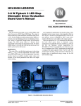
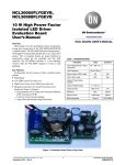
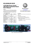
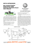
NCP1370BGEVB
NCP1370 Evaluation Board
User's Manual
The NCP1370 is a primary side constant current controller. It
features a built in control algorithm that allows to precisely regulate
the output current of a Flyback converter from the primary side. This
eliminates the need for an opto-coupler and associated circuitry.
The control scheme also support non-isolated topology such as
Buck-Boost and SEPIC. The output current regulation is within ±2%
over a line range of 85 − 265 V rms.
The power control uses a Critical Conduction Mode (CrM)
approach with valley switching to optimize efficiency and EMI
filtering. The controller selects the appropriate valley for operation
which keeps the frequency within a tighter range than would normally
be possible with simple CrM operation.
This manual covers the specification, testing and construction of the
NCP1370 demonstration board. The board demonstrates a 50-W LED
driver for TV backlighting. A dimming circuitry is also provided to
show the dimming performances of the NCP1370.
The board allows building 2 different power converters:
• 200-V Output Voltage with an Output Current of 250 mA
• 100-V Output Voltage with an Output Current of 500 mA
www.onsemi.com
EVAL BOARD USER’S MANUAL
Top View
Specifications
The board is designed to meet the specifications of Table 1.
Table 1. LED Driver Specifications
Symbol
Value
Units
Minimum Input Voltage
Description
VIN,Min
120
V dc
Maximum Input Voltage
VIN,Max
375
V dc
Minimum Output Voltage
VOUT,Min
175
V
Nominal Output Voltage
VOUT,Nom
200
V
Maximum Output Voltage
VOUT,Max
215
V
Output Voltage at which the OVP is
Activated
VOUT(OVP)
340
V
Output Current (Nominal)
IOUT
250
mA
Input Voltage for Brown-In
VIN(Start)
110
V dc
FSW
100
kHz
Switching Frequency at POUT,Max
and VIN,Min
Bottom View
Figure 1. NCP1370 Evaluation Board
Description of the Board
The board has been designed using the method described in the
application note AND9131/D [1].
Figure 2 shows the schematic of the 200-V, 250 mA LED driver
which is the default board version. Figure 3 portrays the schematic of
the 100-V, 500 mA LED driver.
The resistor R12 connected to pin 1 (ILIM) of the controller sets the
peak current limit threshold VILIMIT to 2.4 V. A resistor divided
formed by R34 and R35 is used to limit the voltage and current in ZCD
pin.
R16 is the line feedforward resistor that compensates the output
current variation caused by the propagation delays.
© Semiconductor Components Industries, LLC, 2015
October, 2015 − Rev. 0
1
Publication Order Number:
EVBUM2320/D
NCP1370BGEVB
R23 is used to adjust the output current exactly to 250 mA.
A small output capacitor of 470 nF is used in order to have
a square output current waveform when PWM dimming is
used.
The board has a low profile and its height does not exceed
15 mm.
R1, R3, R5, R7, R8 and R10 are the brown-out resistors
which have been calculated to start operating at
VIN = 110 V dc.
The controller is supplied by an external power supply. In
order to start, the controller needs at least 12 V on VCC pin.
The output current is set to 250 mA by the sense resistors
R17, R18, R20, R21 and R23.
Figure 2. Evaluation Board wit 200-V/250-mA Output
www.onsemi.com
2
NCP1370BGEVB
Figure 3. Evaluation Board wit 100-V/500-mA Output
www.onsemi.com
3
NCP1370BGEVB
Valley Switching and Valley Lockout
keep the switching losses low. For stable operation,
the valley at which the MOSFET is switch-on remains
locked until the light demand is changed. Practically, the
NCP1370 transitions from quasi-resonant operation to the
2nd valley at low line and from 3rd valley to 4th valley at high
line when the LED driver load goes below 80% of its
nominal value. A table summarizing the valley transitions
can be found in the NCP1370 data sheet [2].
The
NCP1370
implements
a
current-mode,
quasi-resonant architecture which optimizes the efficiency
over a wide load range by turning on the MOSFET when its
drain-source voltage is minimal (valley).
Depending on the power supply design, it is possible to
achieve almost zero voltage switching as shown by Figure 4.
When the light is dimmed, the controller selects
a following valley to reduce the switching frequency and
VDRAIN
VDRAIN
VSENSE
VSENSE
Figure 4. 1st Valley Operation at Low Line, Full Load
Figure 5. 3rd Valley Operation at Low High, Full Load
VDRAIN
VDRAIN
Figure 6. 4th Valley Operation at 50% Nominal Output
Current, Low Line
Figure 7. 6th Valley Operation at 50% Output Current,
High Line
Output Current Regulation
In order to compensate the current variation caused by the
propagation delays, line feedforward is needed. The resistor
in series with the CS pin R16 adjust the voltage offset on the
current sense signal as a function of the input voltage.
The capacitor on CS pin C8 must be kept small in order to
avoid delaying the current-sense signal and thus increasing
the propagation delays. Here a capacitor value of 22 pF was
chosen.
Because of the line feedforward and also for reason
inherent to the constant current algorithm, the obtained
output current is slightly lower than the targeted output
current. Thus, it may be necessary to adjust slightly the sense
resistor by decreasing it. That’s why we added R23 = 33 W
in parallel of the other four 3.9 W sense resistors.
The output current value is set by the sense resistor RSENSE
formed by R17, R18, R20, R21 and R23 on the board.
The sense resistor value can be calculated with:
R SENSE +
V REF
2 @ N SP @ I OUT
(eq. 1)
Where:
• NSP is the transformer turn ratio: secondary turns
divided by primary turns
• IOUT is the targeted output current
• VREF is the reference voltage for constant current
regulation
www.onsemi.com
4
NCP1370BGEVB
Output Current (mA)
255
254
175 V
253
200 V
252
220 V
251
250
249
248
247
246
245
120
160
200
240
280
320
360
Input Voltage (V dc)
Figure 8. Output Current Variation for VLED = 175 V to 220 V
265
263
200 V
261
150 V
Output Current (mA)
259
100 V
257
255
253
251
249
247
245
120
160
200
240
280
320
360
Input Voltage (V dc)
Figure 9. Output Current Variation for VLED = 100 V to 200 V
Figure 8 and Figure 9 shows the output current measured
when the input voltage is varied from 120 V dc to 375 V dc
for different LED string voltages. A Chroma electronic load
in LED mode is used to emulate the LED string voltage
variation.
Looking at Figure 8 where the LED voltage is varied from
175 V to 220 V (roughly 200 V ±11%), we can calculate the
mean output current value and the current regulation.
www.onsemi.com
5
NCP1370BGEVB
DI OUT2
The mean output current is calculated by considering the
maximum and the minimum value measured over the output
voltage and the input voltage range:
I OUT,Mean +
+
I OUT,Max ) I OUT,Min
I OUT2
+ 100 @
(eq. 2)
2
253.8 ) 246.8
+ 250.3 mA
2
I OUT
+ 100 @
+ 100 @
I OUT,Max * I OUT,Mean
I OUT,Mean
(eq. 3)
253.8 ) 250.3
+ 1.4%
250.3
+
I OUT2,Max ) I OUT2,Min
(eq. 4)
2
I OUT2,Mean
(eq. 5)
260.9 ) 254.6
+ 2.5%
254.6
A circuit made of the opto-coupler OC1, the transistor Q2
and some resistors is used to send the digital dimming signal
from the secondary side to the DIM pin of the controller on
the primary side.
By default at start-up, the controller is in OFF mode. In
OFF mode, the controller consumes less than 50 mA. The
controller leaves the OFF mode when VCC > VCC(on) and
VDIM > VDIM(EN). During normal operation, the OFF mode
is entered when VDIM stays below VDIM(EN) for 4 seconds.
Back to the evaluation board, in order to start, a voltage of
at least 3.3 V must be applied on P_DIM connector. For
digital or PWM dimming, apply 3.3 V on DRV_ON and
apply a square signal varying between 5 V to 0 V with
a 200-Hz frequency on P_DIM.
By varying the duty-cycle of this signal, the output current
will also vary. Figure 10 shows the output voltage and
current when dimming with 50% duty-cycle. Figure 11
shows the dimming pin voltage VDIM and the drain voltage
in addition to the output current when the dimming signal
has a duty-cycle of 10%. The resistors R12 and R11 with the
capacitor C4 adds in an extra soft-stop which delays the LED
turn-off and compensates the internal soft-start of the
NCP1370 and also the time needed for the output voltage to
be high enough to turn-on the LED.
The output current regulation is thus ±1.4% for a LED
string voltage varying from 175 V to 220 V and for the input
voltage varying from 120 V dc to 375 V dc.
Figure 9 portrays the current variation when the LED
voltage is decreased down to 100 V (the nominal voltage
being 200 V) in order to simulate the case where several
LEDs are shorted.
We can see that the current regulation is still good. We
have 254.6 mA ±2.5%
I OUT2,Mean +
I OUT2,Max * I OUT2,Mean
Dimming
The output current regulation is then calculated as
follows:
DI OUT
+ 100 @
260.9 ) 248.3
+ 254.6 mA
2
VP_DIM
VDIM
VOUT
VP_DIM
VDRAIN
IOUT
IOUT
Figure 10. 50% PWM Dimming
Figure 11. 10% PWM Dimming
www.onsemi.com
6
NCP1370BGEVB
Figure 12 and Figure 13 show the output current as
a function of the PWM dimming signal duty-ratio. The tests
were made at 162 V dc. We can observe that the output
current is nicely controlled by the DIM pin and the measured
current matches the expected value even at low duty-ratio
dimming thanks to the soft-stop.
250
Output Current (mA)
200
150
100
Measured
50
Theoretical
0
0
10
20
30
40
50
60
70
80
90
100
Dimming Duty − Ratio (%)
Figure 12. Output Current vs. PWM Dimming Duty-Ratio
14
Output Current (mA)
12
10
8
6
4
Measured
2
Theoretical
0
0
1
2
3
4
5
6
Dimming Duty − Ratio (%)
Figure 13. Output Current Variation for PWM Dimming Duty-Ration between 1% to 5%
www.onsemi.com
7
NCP1370BGEVB
Over Voltage Protection/Open LED Protection
We chose a 16-V zener diode. As the OVP threshold is 5 V,
the comparator will trigger when the voltage on capacitor C6
exceeds 16 V + 5 V + 0.6 V = 21.6 V (0.6 V being the
forward voltage drop of diode D1).
Figure 14 and Figure 15 show the output voltage
waveform in case of open LED. The maximum output
voltage is 345 V. On Figure 15, we can see that the output
capacitor is discharged down to 0 V after the 1 second timer
has elapsed thanks to the dummy output resistor R32.
By monitoring the auxiliary winding voltage through D3,
D4, R22 and C6, we have an image of the output voltage. By
connecting a zener diode from C6 to the VIN pin, we can
trigger the over voltage protection (OVP). When pin VIN
voltage exceeds 5 V, the controller stops and restarts
switching after 1 second. In order to reach 5 V on VIN pin,
a current of approximately 900 mA must be injected inside
the pin by the zener diode.
VOUT
VOUT
VDRAIN
VDRAIN
Figure 14. VOUT Waveform in Case of Open LED
Figure 15. VOUT Waveform in Case of Open LED after
the OVP Timer Has Elapsed
In order to decrease the maximum voltage reached on the
output connector in case no LEDs are connected to board,
the circuit shown in Figure 16 can be used. The maximum
voltage reached on the board when no LED was connected
was 300 V with this circuit.
VCC
Q4
2N3906
VIN
R102
22k
R103
3.9k
VDRAIN
D3
1N4148
R101
22k
R22
22
D2
18V
D4
1N4937
VOUT
C6
220n
Aux
Q3
2N3904
R9
4.7k
Figure 16. Alternative Circuit for OVP on VIN Pin
Figure 17. Open LED with New OVP Circuit on VIN Pin
As soon as the zener diode starts conducting, the transistor
Q3 is turned on and then bias Q4 which allow pulling the
VIN pin high above 5 V immediately. In this case, we need
to use an 18-V zener diode instead of a 16-V to avoid
triggering the protection during the normal operating range.
www.onsemi.com
8
NCP1370BGEVB
Test Procedure
Equipment Needed:
• High voltage dc source: 100 to 375 V dc, minimum
500 W capability
• Two dc sources, 30 V
• DC Voltmeter – 300 V dc minimum, 0.1% accuracy or
better
• DC Ammeter – 1 A dc minimum, 0.1% accuracy or
better
• LED load between 175 V to 215 V at 250 mA.
A constant voltage Electronic load is an acceptable
substitute as long as it is stable
DC Source
(5 V Setpoint)
DC Ammeter
High Voltage
DC Source
NCP1370EVB
DC Voltmeter
LED
Test Load
DC Source
(14 V Setpoint)
Figure 18.
Test Connections:
• Connect the high voltage source between inputs “+”
and “−” of X1 connector.
• Connect a dc power supply between inputs “VCC” and
“−” of X1 connector
• Connect a dc power supply between inputs 1 and 3 of
X3 connector
• Connect the ammeter to “LED+” output of X2
connector and then connect the LED load positive
terminal to the ammeter and its negative terminal to the
“LED−” output of X2 connector
Functional Test Procedure:
• Set the load at 200 V output
• Set the input voltage to 162 V dc
• Measure the output current: its value should be within
±2% of 250 mA.
www.onsemi.com
9
NCP1370BGEVB
Flyback Inductor Specification
Figure 19. Flyback Inductor Specification
www.onsemi.com
10
NCP1370BGEVB
Bill of Materials
Table 2. NCP1370 BILL OF MATERIALS
Description
Tolerance/
Constraint
Value
Package/
Footprint
Reference
1
C1
1
C10
Ceramic Capacitor
47 pF
5%, 1 kV
Through-Hole
Standard
Standard
1
C12
Film Capacitor PET
470 nF
400 V
Through-Hole
Panasonic
ECQE4474JF
1
C2
Electrolitic Capacitor
1 mF
35 V
Through-Hole
Standard
Standard
2
C3, C6
SMD Capacitor
100 nF
50 V
SMD0805
Standard
Standard
1
C4
SMD Capacitor
1 nF
50 V
SMD0805
Standard
Standard
1
C5
SMD Capacitor
47 pF
50 V
SMD0805
Standard
Standard
1
C7
Electrolitic Capacitor
47 mF
450 V
Through-Hole
Rubycon
12X35
1
C8
SMD Capacitor
22 pF
50 V
SMD0805
Standard
Standard
1
C9
Ceramic Capacitor
1 nF
1 kV
Through-Hole
Standard
Standard
1
CY1
Y1 Capacitor
1 nF
400 V
Through-Hole
Standard
Standard
5
D1, D4, D5,
D7, D10
Standard Diode
1N4148
100 V
SOD−123
ON Semicondutor
MMSD4148
NC
Manufacturer
Manufacturer
Part Number
Qty
SMD0805
1
D2
Zener Diode
BZX85−C16
16 V
DO−41
Fairchild
2
D3, D6
Fast Recovery
Rectifier
1N4937
1 A, 600 V
DO−41
ON Semicondutor
1
D8, D11
Ultra-Fast Diode
MUR160
1 A, 600 V
DO−41
ON Semicondutor
MUR160
1
IC1
PSR Controller
NCP1370B
SO−08
ON Semicondutor
NCP1370B
1
OC1
Opto-Coupler
FOD817B
DIL−04W
Fairchild
FOD817B
1
Q1
Power MOSFET
STD8N80K5
1
Q2
NPN Transistor
BC847A
5
R1, R3, R5,
R7, R8
Resistor
2.2 MW
1
R10
Resistor
6
R11, R12, R19,
R27, R29, R35
2
1
8 A, 800 V
1N4937
DPACK
ST Microelectronics
STD8N80K5
SOT−23
ON Semicondutor
BC847AL
1%, 125 mW
SMD0805
Standard
Standard
100 kW
1%, 125 mW
SMD0805
Standard
Standard
Resistor
10 kW
5%, 125 mW
SMD0805
Standard
Standard
R13, R22
Resistor
22 W
5%, 125 mW
SMD0805
Standard
Standard
R14
Resistor
47 W
5%, 125 mW
SMD0805
Standard
Standard
1
R15
Resistor
47 kW
5%, 1 W
Axial
Standard
Standard
1
R16
Resistor
2.2 kW
1%, 125 mW
SMD0805
Standard
Standard
4
R17, R18, R20,
R21
Resistor
3.9 W
1%, 1 W
SMD2512
Standard
Standard
1
R2
Resistor
12 kW
1%, 125 mW
SMD0805
Standard
Standard
1
R23
Resistor
33 W
1%, 0.5 W
SMD2512
Standard
Standard
1
R24
Resistor
NC
3
R26, R28,
R30
Resistor
22 kW
5%, 125 mW
SMD0805
Standard
Standard
1
R31
Resistor
47 kW
5%, 125 mW
SMD0805
Standard
Standard
1
R32
Resistor
470 kW
5%, 250 mW
Axial
Standard
Standard
1
R33
Resistor
1W
5%, 250 mW
Axial
Standard
Standard
1
R34
Resistor
22 kW
5%, 250 mW
Axial
Standard
Standard
1
R4
Resistor
10 W
5%, 250 mW
Axial
Standard
Standard
1
R6
Resistor
0W
5%, 250 mW
Axial
Standard
Standard
2
R9, R25
Resistor
4.7 kW
5%, 125 mW
SMD0805
Standard
Standard
1
TR1
Flyback Inductor
Through-Hole
Wurth
750315357
1
X1
Input Connector
Through-Hole
Standard
Standard
1
X2
Output Connector
Through-Hole
Standard
Standard
1
X3
Dimming Connector
Through-Hole
Standard
Standard
SMD2512
www.onsemi.com
11
NCP1370BGEVB
References
[1] Stéphanie Cannenterre, Application note
AND9131/D, “Designing a LED Driver with the
NCL30080/81/82/83”
[2] Data Sheet NCP1370/D
ON Semiconductor and the
are registered trademarks of Semiconductor Components Industries, LLC (SCILLC) or its subsidiaries in the United States and/or other countries.
SCILLC owns the rights to a number of patents, trademarks, copyrights, trade secrets, and other intellectual property. A listing of SCILLC’s product/patent coverage may be accessed
at www.onsemi.com/site/pdf/Patent−Marking.pdf. SCILLC reserves the right to make changes without further notice to any products herein. SCILLC makes no warranty, representation
or guarantee regarding the suitability of its products for any particular purpose, nor does SCILLC assume any liability arising out of the application or use of any product or circuit, and
specifically disclaims any and all liability, including without limitation special, consequential or incidental damages. “Typical” parameters which may be provided in SCILLC data sheets
and/or specifications can and do vary in different applications and actual performance may vary over time. All operating parameters, including “Typicals” must be validated for each
customer application by customer’s technical experts. SCILLC does not convey any license under its patent rights nor the rights of others. SCILLC products are not designed, intended,
or authorized for use as components in systems intended for surgical implant into the body, or other applications intended to support or sustain life, or for any other application in which
the failure of the SCILLC product could create a situation where personal injury or death may occur. Should Buyer purchase or use SCILLC products for any such unintended or
unauthorized application, Buyer shall indemnify and hold SCILLC and its officers, employees, subsidiaries, affiliates, and distributors harmless against all claims, costs, damages, and
expenses, and reasonable attorney fees arising out of, directly or indirectly, any claim of personal injury or death associated with such unintended or unauthorized use, even if such claim
alleges that SCILLC was negligent regarding the design or manufacture of the part. SCILLC is an Equal Opportunity/Affirmative Action Employer. This literature is subject to all applicable
copyright laws and is not for resale in any manner.
PUBLICATION ORDERING INFORMATION
LITERATURE FULFILLMENT:
Literature Distribution Center for ON Semiconductor
19521 E. 32nd Pkwy, Aurora, Colorado 80011 USA
Phone: 303−675−2175 or 800−344−3860 Toll Free USA/Canada
Fax: 303−675−2176 or 800−344−3867 Toll Free USA/Canada
Email: [email protected]
N. American Technical Support: 800−282−9855 Toll Free
USA/Canada
Europe, Middle East and Africa Technical Support:
Phone: 421 33 790 2910
Japan Customer Focus Center
Phone: 81−3−5817−1050
www.onsemi.com
12
ON Semiconductor Website: www.onsemi.com
Order Literature: http://www.onsemi.com/orderlit
For additional information, please contact your local
Sales Representative
EVBUM2320/D