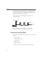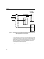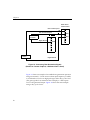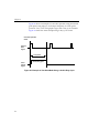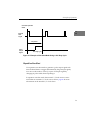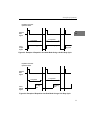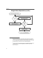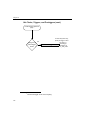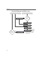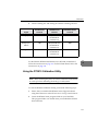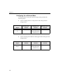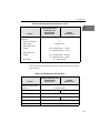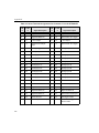
1
UM-16866-E DT3010 Series User’s Manual Fifth Edition March, 2002 Copyright © 1998, 2000, 2001, 2002 by Data Translation, Inc. All rights reserved. No part of this publication may be reproduced, stored in a retrieval system, or transmitted, in any form by any means, electronic, mechanical, by photocopying, recording, or otherwise, without the prior written permission of Data Translation, Inc. Information furnished by Data Translation, Inc. is believed to be accurate and reliable; however, no responsibility is assumed by Data Translation, Inc. for its use; nor for any infringements of patents or other rights of third parties which may result from its use. No license is granted by implication or otherwise under any patent rights of Data Translation, Inc. Use, duplication, or disclosure by the United States Government is subject to restrictions as set forth in subparagraph (c)(1)(ii) of the Rights in Technical Data and Computer software clause at 48 C.F.R, 252.227-7013, or in subparagraph (c)(2) of the Commercial computer Software Registered Rights clause at 48 C.F.R., 52-227-19 as applicable. Data Translation, Inc., 100 Locke Drive, Marlboro, MA 01752 Data Translation, Inc. 100 Locke Drive Marlboro, MA 01752-1192 (508) 481-3700 www.datatranslation.com Fax: (508) 481-8620 E-mail: [email protected] Data Translation® is a registered trademark of Data Translation, Inc. DT-Open LayersTM, DataAcq SDKTM , Data Acquisition OMNI CDTM, DT-LV LinkTM , DTx-EZTM, and DT VPI TM are trademarks of Data Translation, Inc. All other brand and product names are trademarks or registered trademarks of their respective companies. Radio and Television Interference This equipment has been tested and found to comply with CISPR EN55022 Class A and EN50082-1 (CE) requirements and also with the limits for a Class A digital device, pursuant to Part 15 of the FCC Rules. These limits are designed to provide reasonable protection against harmful interference when the equipment is operated in a commercial environment. This equipment generates, uses, and can radiate radio frequency energy and, if not installed and used in accordance with the instruction manual, may cause harmful interference to radio communications. Operation of this equipment in a residential area is likely to cause harmful interference, in which case the user will be required to correct the interference at his own expense. Changes or modifications to this equipment not expressly approved by Data Translation could void your authority to operate the equipment under Part 15 of the FCC Rules. Note: This product was verified to meet FCC requirements under test conditions that included use of shielded cables and connectors between system components. It is important that you use shielded cables and connectors to reduce the possibility of causing interference to radio, television, and other electronic devices. Canadian Department of Communications Statement This digital apparatus does not exceed the Class A limits for radio noise emissions from digital apparatus set out in the Radio Interference Regulations of the Canadian Department of Communications. Le présent appareil numérique n’émet pas de bruits radioélectriques dépassant les limites applicables aux appareils numériques de la class A prescrites dans le Règlement sur le brouillage radioélectrique édicté par le Ministère des Communications du Canada. Table of Contents About this Manual . . . . . . . . . . . . . . . . . . . . . . . . . . . . . . . . . . xi Intended Audience. . . . . . . . . . . . . . . . . . . . . . . . . . . . . . . . . . . . . . xi What You Should Learn from this Manual. . . . . . . . . . . . . . . . . . xi Conventions Used in this Manual . . . . . . . . . . . . . . . . . . . . . . . . . xii Related Information . . . . . . . . . . . . . . . . . . . . . . . . . . . . . . . . . . . . xiii Where To Get Help. . . . . . . . . . . . . . . . . . . . . . . . . . . . . . . . . . . . . xiv Chapter 1: Overview . . . . . . . . . . . . . . . . . . . . . . . . . . . . . . . . 1 Features . . . . . . . . . . . . . . . . . . . . . . . . . . . . . . . . . . . . . . . . . . . . . . . . 2 Supported Software . . . . . . . . . . . . . . . . . . . . . . . . . . . . . . . . . . . . . . 5 Accessories . . . . . . . . . . . . . . . . . . . . . . . . . . . . . . . . . . . . . . . . . . . . . 7 Chapter 2: Principles of Operation . . . . . . . . . . . . . . . . . . . . 9 Analog Input Features . . . . . . . . . . . . . . . . . . . . . . . . . . . . . . . . . . . 11 Analog Input Resolution . . . . . . . . . . . . . . . . . . . . . . . . . . . . . 11 Analog Input Channels . . . . . . . . . . . . . . . . . . . . . . . . . . . . . . 11 Specifying a Single Channel . . . . . . . . . . . . . . . . . . . . . . 12 Specifying One or More Channels . . . . . . . . . . . . . . . . . 12 Specifying Digital Input Lines in the Analog Input Channel List . . . . . . . . . . . . . . . . . . . . . . . . . . 13 Performing Dynamic Digital Output Operations . 14 Input Ranges and Gains. . . . . . . . . . . . . . . . . . . . . . . . . . . . . . 15 Specifying the Gain for a Single Channel . . . . . . . . . . . 16 Specifying the Gain for One or More Channels . . . . . . 17 A/D Sample Clock Sources . . . . . . . . . . . . . . . . . . . . . . . . . . . 17 Internal A/D Sample Clock . . . . . . . . . . . . . . . . . . . . . . . 18 External A/D Sample Clock . . . . . . . . . . . . . . . . . . . . . . 19 Analog Input Conversion Modes . . . . . . . . . . . . . . . . . . . . . . 20 v Contents Continuously-Paced Scan Mode . . . . . . . . . . . . . . . . . . . 21 Triggered Scan Mode . . . . . . . . . . . . . . . . . . . . . . . . . . . . 22 Internally-Retriggered Scan Mode . . . . . . . . . . . . . . 22 Externally-Retriggered Scan Mode . . . . . . . . . . . . . 24 Triggers . . . . . . . . . . . . . . . . . . . . . . . . . . . . . . . . . . . . . . . . . . . . 26 Trigger Sources . . . . . . . . . . . . . . . . . . . . . . . . . . . . . . . . . 26 Software Trigger . . . . . . . . . . . . . . . . . . . . . . . . . . . . . 27 External Digital (TTL) Trigger. . . . . . . . . . . . . . . . . . 27 Analog Threshold Trigger . . . . . . . . . . . . . . . . . . . . . 28 Trigger Acquisition Modes . . . . . . . . . . . . . . . . . . . . . . . 29 Post-Trigger Acquisition . . . . . . . . . . . . . . . . . . . . . . 29 Pre-Trigger Acquisition . . . . . . . . . . . . . . . . . . . . . . . 31 About-Trigger Acquisition . . . . . . . . . . . . . . . . . . . . 33 Data Format and Transfer . . . . . . . . . . . . . . . . . . . . . . . . . . . . 36 Error Conditions . . . . . . . . . . . . . . . . . . . . . . . . . . . . . . . . . . . . 38 Analog Output Features . . . . . . . . . . . . . . . . . . . . . . . . . . . . . . . . . 40 Analog Output Resolution. . . . . . . . . . . . . . . . . . . . . . . . . . . . 40 Analog Output Channels . . . . . . . . . . . . . . . . . . . . . . . . . . . . . 41 Specifying a Single Channel . . . . . . . . . . . . . . . . . . . . . . 41 Specifying One or More Channels . . . . . . . . . . . . . . . . . 41 Output Filters. . . . . . . . . . . . . . . . . . . . . . . . . . . . . . . . . . . . . . . 42 Output Ranges and Gains . . . . . . . . . . . . . . . . . . . . . . . . . . . . 42 D/A Output Clock Sources . . . . . . . . . . . . . . . . . . . . . . . . . . . 42 Internal D/A Output Clock . . . . . . . . . . . . . . . . . . . . . . . 43 External D/A Output Clock . . . . . . . . . . . . . . . . . . . . . . 43 Trigger Sources . . . . . . . . . . . . . . . . . . . . . . . . . . . . . . . . . . . . . 44 Software Trigger . . . . . . . . . . . . . . . . . . . . . . . . . . . . . . . . 44 External Digital (TTL) Trigger . . . . . . . . . . . . . . . . . . . . . 44 Analog Threshold Trigger . . . . . . . . . . . . . . . . . . . . . . . . 45 vi Contents Analog Output Conversion Modes . . . . . . . . . . . . . . . . . . . . 46 Continuously-Paced Analog Output . . . . . . . . . . . . . . . 47 Waveform Generation . . . . . . . . . . . . . . . . . . . . . . . . . . . 48 Data Format and Transfer . . . . . . . . . . . . . . . . . . . . . . . . . . . . 49 Error Conditions . . . . . . . . . . . . . . . . . . . . . . . . . . . . . . . . . . . . 51 Digital I/O Features . . . . . . . . . . . . . . . . . . . . . . . . . . . . . . . . . . . . . 52 Digital I/O Lines . . . . . . . . . . . . . . . . . . . . . . . . . . . . . . . . . . . . 52 Digital I/O Resolution . . . . . . . . . . . . . . . . . . . . . . . . . . . . . . . 53 Digital I/O Operation Modes . . . . . . . . . . . . . . . . . . . . . . . . . 53 Counter/Timer Features . . . . . . . . . . . . . . . . . . . . . . . . . . . . . . . . . 55 Units . . . . . . . . . . . . . . . . . . . . . . . . . . . . . . . . . . . . . . . . . . . . . . 55 C/T Clock Sources . . . . . . . . . . . . . . . . . . . . . . . . . . . . . . . . . . 56 Internal C/T Clock . . . . . . . . . . . . . . . . . . . . . . . . . . . . . . 56 External C/T Clock. . . . . . . . . . . . . . . . . . . . . . . . . . . 56 Internally Cascaded Clock . . . . . . . . . . . . . . . . . . . . . . . . 58 Gate Types . . . . . . . . . . . . . . . . . . . . . . . . . . . . . . . . . . . . . . . . . 59 Pulse Output Types and Duty Cycles . . . . . . . . . . . . . . . . . . 60 Counter/Timer Operation Modes . . . . . . . . . . . . . . . . . . . . . 62 Event Counting . . . . . . . . . . . . . . . . . . . . . . . . . . . . . . . . . . . . . 63 Frequency Measurement . . . . . . . . . . . . . . . . . . . . . . . . . 65 Rate Generation . . . . . . . . . . . . . . . . . . . . . . . . . . . . . . . . . 69 One-Shot . . . . . . . . . . . . . . . . . . . . . . . . . . . . . . . . . . . . . . . 72 Repetitive One-Shot . . . . . . . . . . . . . . . . . . . . . . . . . . . . . 75 Synchronizing A/D and D/A Subsystems . . . . . . . . . . . . . . . . . 78 Synchronizing the Triggers . . . . . . . . . . . . . . . . . . . . . . . . . . . 78 Synchronizing the Clocks. . . . . . . . . . . . . . . . . . . . . . . . . . . . . 79 Chapter 3: Supported Capabilities. . . . . . . . . . . . . . . . . . . . 81 vii Contents Chapter 4: Programming Flowcharts. . . . . . . . . . . . . . . . . . 93 Single-Value Operations . . . . . . . . . . . . . . . . . . . . . . . . . . . . . . . . . 95 Continuous A/D Operations . . . . . . . . . . . . . . . . . . . . . . . . . . . . . 97 Continuous D/A Operations . . . . . . . . . . . . . . . . . . . . . . . . . . . . . 99 Event Counting Operations . . . . . . . . . . . . . . . . . . . . . . . . . . . . . 101 Frequency Measurement Operations . . . . . . . . . . . . . . . . . . . . . 103 Pulse Output Operations. . . . . . . . . . . . . . . . . . . . . . . . . . . . . . . . 105 Simultaneous Operations . . . . . . . . . . . . . . . . . . . . . . . . . . . . . . . 107 Chapter 5: Calibration . . . . . . . . . . . . . . . . . . . . . . . . . . . . . 125 Calibrating the Analog Input Subsystem . . . . . . . . . . . . . . . . . . 127 Choosing a Calibration Reference. . . . . . . . . . . . . . . . . . . . . 127 Configuring for the Internal Reference . . . . . . . . . . . . 128 Configuring for an External Reference . . . . . . . . . . . . 129 Using the DT3010 Calibration Utility. . . . . . . . . . . . . . . . . . 131 Using the Auto-Calibration Procedure . . . . . . . . . . . . 132 Using the Manual Calibration Procedure . . . . . . . . . . 133 Calibrating the PGH Zero Setting . . . . . . . . . . . . . . . . . 135 Using the DT3016 Calibration Utility. . . . . . . . . . . . . . . . . . 136 Using the Auto-Calibration Procedure . . . . . . . . . . . . 137 Calibrating the PGH Zero Setting . . . . . . . . . . . . . . . . . 139 Calibrating the Analog Output Subsystem . . . . . . . . . . . . . . . . 141 Choosing a Calibration Meter . . . . . . . . . . . . . . . . . . . . . . . . 141 Configuring for the Internal ADC . . . . . . . . . . . . . . . . 142 Configuring for an External Meter . . . . . . . . . . . . . . . . 144 Using the DT3010 Calibration Utility. . . . . . . . . . . . . . . . . . 146 Using the DT3016 Calibration Utility. . . . . . . . . . . . . . . . . . 148 viii Contents Chapter 6: Troubleshooting . . . . . . . . . . . . . . . . . . . . . . . . 151 Service and Support . . . . . . . . . . . . . . . . . . . . . . . . . . . . . . . . . . . . 155 Telephone Technical Support. . . . . . . . . . . . . . . . . . . . . . . . . 155 E-Mail and Fax Support . . . . . . . . . . . . . . . . . . . . . . . . . . . . . 158 World-Wide Web . . . . . . . . . . . . . . . . . . . . . . . . . . . . . . . . . . . 158 If Your Board Needs Factory Service. . . . . . . . . . . . . . . . . . . . . . 159 Appendix A: Specifications . . . . . . . . . . . . . . . . . . . . . . . . 161 Appendix B: Connector Pin Assignments . . . . . . . . . . . . 175 Index . . . . . . . . . . . . . . . . . . . . . . . . . . . . . . . . . . . . . . . . . . . . 197 ix Contents x About this Manual This manual describes the features of the DT3010, DT3010-268, DT3010/32, DT3010/32-268, and DT3016 boards (collectively referred to as the DT3010 Series), the capabilities of the DT3010 Series Device Driver, and how to program the DT3010 Series board using DT-Open Layers software. Troubleshooting and calibration information is also provided. Intended Audience This document is intended for engineers, scientists, technicians, or others responsible for using and/or programming the DT3010 Series boards for data acquisition operations in Microsoft® Windows® 98, Windows Me (Millennium Edition), Windows NT® 4.0, Windows 2000, or Windows XP. It is assumed that you have some familiarity with data acquisition principles, and that you understand your application. What You Should Learn from this Manual This manual provides detailed information about the features of the DT3010 Series boards and the capabilities of the DT3010 Series Device Driver. It is organized as follows: • Chapter 1, “Overview,” describes the major features of the board, as well as the supported software and accessories for the board. • Chapter 2, “Principles of Operation,” describes all of the board’s features and how to use them in your application. • Chapter 3, “Supported Capabilities,” lists the data acquisition subsystems and the associated features accessible using the DT3010 Series Device Driver. xi About this Manual • Chapter 4, “Programming Flowcharts,” describes the processes you must follow to program the subsystems on the DT3010 Series board using DT-Open Layers-compliant software. • Chapter 5, “Calibration,” describes how to calibrate the analog I/O circuitry of the board. • Chapter 6, “Troubleshooting,” provides information that you can use to resolve problems with the board and the device driver, should they occur. • Appendix A, “Specifications,” lists the specifications of the board. • Appendix B, “Connector Pin Assignments,” shows the pin assignments for the connectors on the board and for the DT740, STP268, and STP268-EC screw terminal panels. • An index completes this manual. Conventions Used in this Manual The following conventions are used in this manual: • Notes provide useful information or information that requires special emphasis, cautions provide information to help you avoid losing data or damaging your equipment, and warnings provide information to help you avoid catastrophic damage to yourself or your equipment. • Items that you select or type are shown in bold. xii About this Manual Related Information Refer to the following documents for more information on using the DT3010 Series board: • DT3010 Series Getting Started Manual (UM-16868). This manual describes how to install the DT3010 Series boards, support software, and device driver; verify the operation of the board; and view the DT3010 Series documentation online. This manual is provided on the Data Acquisition OMNI CDTM. • DT Measure Foundry Getting Started Manual (UM-19298) and online help. These documents describe how to use DT Measure Foundry™ to build drag-and-drop test and measurement applications for Data Translation® data acquisition devices without programming. • DataAcq SDK User’s Manual (UM-18326). For programmers who are developing their own application programs using the Microsoft C compiler, this manual describes how to use the DT-Open Layers DataAcq SDKTM to access the capabilities of Data Translation data acquisition boards. This manual is provided on the Data Acquisition OMNI CD. • DTx-EZ Getting Started Manual (UM-15428). This manual, available from Data Translation, describes how to use the ActiveX controls provided in DTx-EZTM to access the capabilities of Data Translation data acquisition boards in Microsoft® Visual BasicTM or Visual C++. • DT VPI User Manual (UM-16150). This manual, available from Data Translation, describes how to use DT VPITM and the Agilent® VEE™ visual programming language to access the capabilities of Data Translation data acquisition boards. • DT-LV Link Getting Started Manual (UM-15790). This manual, available from Data Translation, describes how to use DT-LV LinkTM with the LabVIEW® graphical programming language to access the capabilities of Data Translation data acquisition boards. xiii About this Manual • PCI Specification: PCI Local Bus Specification, PCI Special Interest Group, Portland, OR. (Revision 2.1, June 1, 1995). • Microsoft Windows 98, Windows Me, Windows NT 4.0, Windows 2000, or Windows XP user manuals. Where To Get Help Should you run into problems installing or using a DT3010 Series board, our Technical Support Department is available to provide prompt, technical assistance. Refer to Chapter 6 for more information. If you are outside the U.S. or Canada, call your local distributor, whose number is listed in your Data Translation product handbook. xiv 1 Overview Features . . . . . . . . . . . . . . . . . . . . . . . . . . . . . . . . . . . . . . . . . . . . . . . . 2 Supported Software . . . . . . . . . . . . . . . . . . . . . . . . . . . . . . . . . . . . . . 5 Accessories . . . . . . . . . . . . . . . . . . . . . . . . . . . . . . . . . . . . . . . . . . . . . 7 1 Chapter 1 Features The DT3010 Series consists of the following high-speed, multifunction board types for the PCI bus: DT3010, DT3010-268, DT3010/32, DT3010/32-268 and DT3016. These board types differ in analog I/O resolution, output FIFO (first-in, first-out buffer) size, throughput, D/A filters, and connectors as shown in Table 1. Table 1: Differences Among DT3010 Series Boards Board Type Analog I/O Resolution Output FIFO Size A/D Throughputa D/A Throughputb D/A Filters DT3010 12 bits 4 kSamples 1.25 MSamples/s 200 kSamples/s − one 50-pin, one 68-pin DT3010 -268 12 bits 4 kSamples 1.25 MSamples/s 200 kSamples/s − two 68-pin DT3010 /32 12 bits 32 kSamples 1.25 MSamples/s 200 kSamples/s − one 50-pin, one 68-pin DT3010 /32-268 12 bits 32 kSamples 1.25 MSamples/s 200 kSamples/s − two 68-pin DT3016 16 bits 4 kSamples 250 kSamples/s 100 kSamples/s 0 and 20 kHz one 50-pin, one 68-pin Connectors a. This throughput is for a single analog input channel. b. This throughput is for full-scale ranges. All DT3010 Series boards share the following major features: • 32 Single-ended or pseudo-differential analog input channels, or 16 differential analog input channels; • Programmable bipolar (±10 V) and unipolar (0 to 10 V) input ranges with gains of 1, 2, 4, and 8; 2 Overview • Continuously-paced and triggered scan capability; • A 1024-location channel-gain list that supports sampling analog input channels at the same or different gains in sequential or random order; • Up to 256 scans per trigger for a total of 262,144 samples per trigger; 1 1 • PCI bus mastering for data transfers; • Pre-, post-, and about-trigger acquisition modes to acquire data relative to an external event using computer memory; • Internal and external clock sources; one external clock input for the analog input subsystem and one external clock input for the analog output subsystem; • Analog threshold triggering using either an external analog input or one of the analog input channels; a separate DAC sets the trigger level (8-bit resolution, fixed hysteresis); • Digital TTL triggering; one external hardware TTL input for the analog input subsystem and one external hardware TTL input for the analog output subsystem; • Two analog output channels with a ±10 V output range; • Simultaneous analog input and analog output operations running at full speed; • Software calibration of the analog input and output subsystems; • Two 8-bit digital ports programmable as inputs or outputs on a per-port basis; digital inputs can be included as part of the analog input channel-gain list to correlate the timing of analog and digital events; digital outputs can drive external solid-state relays; • Two dynamic, high-speed digital output lines; useful for synchronizing and controlling external equipment, these dynamic digital output lines are programmable as part of the analog input subsystem; 1 1 1 1 1 1 1 3 Chapter 1 • Four user counter/timers programmable for event counting, frequency measurement, rate generation (continuous pulse output), one-shot pulse output, and repetitive one-shot pulse output; • Programmable gate types; • Programmable pulse output polarities (output types) and duty cycles; and • A/D Sample Clock Output and A/D Trigger Output signals, useful for synchronizing and controlling external equipment. • For a discussion of these features in detail, refer to Chapter 2. 4 Overview Supported Software The following software is available for use with the DT3010 Series boards: • DT3010 Series Device Driver − This software is included on the Data Acquisition OMNI CD that is shipped with the board. You must install this DT3010 Series software, which installs the device driver, to use the DT3010 Series board with any of the supported software packages or utilities. Refer to the DT3010 Series Getting Started Manual (UM-16868) for more information on installing the software. • The Quick Data Acq application − This software is shipped with the board on the Data Acquisition OMNI CD. This application provides a quick way to get a DT3010 Series board up and running. Using the Quick Data Acq application, you can verify the features of the board, display data on the screen, and save data to disk. Refer to the DT3010 Series Getting Started Manual (UM-16868) for information on using the Quick Data Acq application. • Scope application − This software is shipped with the board on the Data Acquisition OMNI CD. This application emulates three basic instruments: a simple oscilloscope chart recorder, a data logger, and a multi-channel oscilloscope. Using the Scope application, you can monitor data online and capture it to disk. Refer to the online documentation provided on the CD-ROM for more information. • DT3010 and DT3016 Calibration Utilities − This software is shipped with the board on the Data Acquisition OMNI CD. The DT3010 Calibration Utility allows you to calibrate the analog input and analog output subsystems of the DT3010, DT3010-268, DT3010/32, and DT3010/32-268 boards. The DT3016 Calibration Utility allows you to calibrate the analog input and analog output subsystems of the DT3016 board. Refer to page 125 for more information on these utilities. 1 1 1 1 1 1 1 1 1 5 Chapter 1 • DT Measure Foundry − An evaluation version of this software is included on the Data Acquisition OMNI CD. DT Measure Foundry is drag-and-drop test and measurement application builder designed to give you top performance with ease-of-use development. Order the full development version of this software package to develop your own application using real hardware. • DataAcq SDK − This software is shipped on the Data Acquisition OMNI CD. Use the Data Acq SDK if you want to use Windows 98, Windows Me, Windows NT 4.0, Windows 2000, or Windows XP to develop your own application software for the DT3010 Series boards using the Microsoft C compiler; the DataAcq SDK complies with the DT-Open Layers standard. • DTx-EZ − Order this optional software package if you want to use ActiveX controls to access the capabilities of the DT3010 Series boards using Microsoft Visual Basic or Visual C++; DTx-EZ complies with the DT-Open Layers standard. • DT VPI − Order this optional software package if you want to use the Aglient VEE visual programming language to access the capabilities of the DT3010 Series boards. • DT-LV Link − Order this optional software package if you want to use the LabVIEW graphical programming language to access the capabilities of the DT3010 Series boards. • Testpoint − Order this optional software package if you want use a drag-and-drop software environment for designing test, measurement, and data acquisition applications. Refer to the catalog to determine the appropriate software package for your application. 6 Overview Accessories The following optional accessories are available for DT3010 Series boards: • DT740 screw terminal panel − Screw terminal panel with two connectors to accommodate the analog I/O, digital I/O, and counter/timer signals provided by the DT3010, DT3010/32, DT3010/32-268, and DT3016 boards. 1 1 • EP307 cable − A 1-meter, twisted-pair, shielded cable that connects the 50-pin analog I/O connector (J1) on the DT3010, DT3010/32, DT3010/32-268, and DT3016 boards to the J1 connector on the DT740 screw terminal panel. 1 • EP308 cable − A 1-meter, twisted-pair, shielded cable that connects the 68-pin digital I/O connector (J2) on the DT3010, DT3010/32, DT3010/32-268, and DT3016 boards to the J2 connector on the DT740 screw terminal panel. 1 • STP268 screw terminal panel − Screw terminal panel with one 68-pin connector to access the signals provided by one of the connectors on the DT3010-268 board. If you want to access all of the functionality of the DT3010-268 at the same time, you need two STP268 screw terminal panels. • STP268-EC screw terminal panel − Screw terminal panel with two 26-pin connectors for attaching to 5B or 7B Series signal conditioning backplanes, one 50-pin connector for attaching to the Opto-22 PB16H backplane, and one 68-pin connector for attaching to the DT3010-268 board. • EP324 cable − A 1 1/2-inch ribbon cable that connects to the 68-pin digital I/O connector (J2) on the DT3010-268 board; the other end of this cable provides a 68-pin connector and face plate for connection to an EP325 cable. This cable is shipped with each DT3010-268 board. • EP325 cable − A, 6-foot, SCSI-3 cable that connects the STP268 or STP268-EC screw terminal panel to connector J1 on the DT3010-268 board. 1 1 1 1 1 7 Chapter 1 • 5B01 − a 16-channel backplane that accepts 5B Series signal conditioning modules. • 5B08 − an 8-channel backplane that accepts 5B Series signal conditioning modules. • 7BP16-1 − a 16-channel backplane that accepts 7B Series signal conditioning modules. • 7BP08-1 − an 8-channel backplane that accepts 7B Series signal conditioning modules. • 7BP04-1 − a 4-channel backplane that accepts 7B Series signal conditioning modules. • PB16H − a digital backplane that connects to the STP268-EC screw terminal panel to allow access to digital I/O signals. • AC1315 − a 2-foot, 26-pin female to 26-pin female cable that connects a 5B Series backplane to an STP268-EC screw terminal panel. • AC1393 − a 6-inch, 26-pin male to 25-pin female adapter cable that connects a 7B Series backplane to the AC1315 cable; the AC1315 cable then connects to an STP268-EC screw terminal panel. • EP035 − a 2.4-meter, 50-pin ribbon cable that connects the PB16H Opto 22 backplane to an STP268-EC screw terminal panel. 8 2 Principles of Operation Analog Input Features . . . . . . . . . . . . . . . . . . . . . . . . . . . . . . . . . . . 11 Analog Output Features . . . . . . . . . . . . . . . . . . . . . . . . . . . . . . . . . 40 Digital I/O Features . . . . . . . . . . . . . . . . . . . . . . . . . . . . . . . . . . . . . 52 Counter/Timer Features . . . . . . . . . . . . . . . . . . . . . . . . . . . . . . . . . 55 Synchronizing A/D and D/A Subsystems . . . . . . . . . . . . . . . . . 78 9 Chapter 2 This chapter describes the analog input, analog output, digital I/O, counter/timer, and synchronous features of the DT3010 Series boards. To frame the discussions, refer to the block diagram shown in Figure 1. Note that bold entries indicate signals you can access. A/D Trig Trigger/Clock Logic Ext A/D Clock Ext A/D TTL Trig Ext D/A Clock Ext D/A TTL Trig A/D Trig A/D Counter, 24-bits A/D Clk D/A Counter 24-bit D/A Clk 20 MHz Clock A/D Clk Out 1 K Entry CGL FIFO CGL Reg. Channel Parameter Reg. TScan Counter 24-bit Analog Trigger A/D Trig Out Buffer A/D Clk Ext Analog Trigger Analog In Ch. Sel Gain Sel A/D Clk Output FIFO* 32 Channel Mux Output FIFO Counter 12- or 16-bit Analog Out 1 DAC** Gain Amp (1, 2, 4, 8) 12- or 16-bit ADC** D/A Clk MUX 8-bit DAC 12- or 16-bitAnalog Out 0 DAC** DIO Bank B [7:0] Bidirectional 8-bit Latch DIO Ports Input Sel Ch. Sel Gain Sel Input Sel Compare 1 kSample Input FIFO Analog Trigger DIO Bank A [7:0] Bidirectional 8-bit Latch Tristate Buffers 20 MHz Clk 4 User Counter/ Timers, 16-bit ea. User Clk [3:0] User Gate [3:0] User Out [3:0] PCI Bus Interface PCI Bus *The DT3010, DT3010-268, and DT3016 have a 4 kSample output FIFO; the DT3010/32 and DT3010/32-268 have a 32 kSample output FIFO.**Only the DT3016 has a 16-bit ADC and 16-bit DACs. Figure 1: Block Diagram of the DT3010 Series Boards 10 Principles of Operation Analog Input Features This section describes the features of the analog input (A/D) subsystem, including the following: • Analog input resolution, • Analog input channels, 2 2 • Input ranges and gains, • A/D sample clock sources, • Analog input conversion modes, 2 • Trigger sources and trigger acquisition modes, • Data formats and transfer, and • Error conditions. Analog Input Resolution DT3010, DT3010-268, DT3010/32, and DT3010/32-268 boards have a fixed analog input resolution of 12 bits. The DT3016 board has a fixed resolution of 16 bits. The analog input resolution cannot be changed in software. Analog Input Channels DT3010 Series boards support 32 single-ended or pseudo-differential analog input channels, or 16 differential analog input channels. Refer to the DT3010 Series Getting Started Manual for a description of how to wire these signals. Use software to specify the channel type. 2 2 2 2 2 2 11 Chapter 2 Note: For pseudo-differential inputs, specify single-ended in software; in this case, how you wire these signals determines the configuration. DT3010 Series boards can acquire data from a single analog input channel or from a group of analog input channels. Channels are numbered 0 to 31 for single-ended and pseudo-differential inputs, and 0 to 15 for differential inputs. The following subsections describe how to specify the channels. Specifying a Single Channel The simplest way to acquire data from a single channel is to specify the channel for a single-value analog input operation using software; refer to page 20 for more information on single-value operations. You can also specify a single channel using the analog input channel list, described in the next section. Specifying One or More Channels DT3010 Series boards can read data from one or more analog input channels using an analog input channel list. You can group the channels in the list sequentially (either starting with 0 or with any other analog input channel), or randomly. You can also specify a single channel or the same channel more than once in the list. Using software, specify the channels in the order you want to sample them. The analog input channel list corresponds to the Channel-Gain List FIFO on the board. You can enter up to 1,024 entries. The channels are read in order (using continuously- paced scan mode or triggered scan mode) from the first entry to the last entry in the channel list. The board can read the channels in the channel list up to 256 times per trigger (for a total of 262,144 samples per trigger) using 12 Principles of Operation triggered scan mode. Refer to page 20 for more information on the supported conversion modes. If you wish, you can also use software to set up a channel-inhibit list. This feature is useful if you want to discard acquired values from specific entries in the channel list. Using the channel-inhibit list, you can enable or disable inhibition for each entry in the analog input channel list. If enabled, the value is discarded after the channel is read; if disabled, the value is not discarded after the channel is read. 2 2 2 Note: If you select an analog input channel as the analog threshold trigger source, the channel used for this trigger source must be the first channel specified in the analog input channel list; refer to page 28 for more information on this trigger source. 2 Specifying Digital Input Lines in the Analog Input Channel List 2 In addition to the analog input channels, you can read the 16 digital I/O lines (Bank A 0 to 7 and Bank B 0 to 7) of the DT3010 Series boards using the analog input channel list. This feature is particularly useful when you want to correlate the timing of analog and digital events. 2 To read these 16 digital I/O lines, specify channel 32 in the analog input channel list. You can enter channel 32 anywhere in the list and can enter it more than once, if desired. 2 This channel is treated like any other channel in the analog input channel list; therefore, all the clocking, triggering, and conversion modes supported for analog input channels are supported for these digital I/O lines, if you specify them in this manner. 2 2 13 Chapter 2 Performing Dynamic Digital Output Operations Using software, you can enable a synchronous dynamic digital output operation for the A/D subsystem. This feature is particularly useful for synchronizing and controlling external equipment. Two dynamic digital output lines are provided: 0 and 1. These lines are set to a value of 0 on power up; a reset does not affect the values of the dynamic digital output lines. Note that these lines are provided in addition to the other 16 digital I/O lines; see page 52 for more information on the digital I/O features. Using software, specify the values to write to the dynamic digital output lines using the analog input channel list. As each entry in the analog input channel list is read, the corresponding value you specified is output to the dynamic digital output lines. For DT3010 Series boards, you can specify the following values for the dynamic digital output lines: 0 (00 in binary format), 1 (01 in binary format), 2 (10 in binary format), or 3 (11 in binary format), where a value of 1 means that the line goes high and a value of 0 means that the line goes low. Each bit in binary format corresponds to the value to write to the dynamic digital output line. For example, a value of 1 (01 in binary format) means that a value of 1 is output to dynamic digital output line 0 and value of 0 is output to dynamic output line 1. Similarly, a value of 2 (10 in binary format) means that a value of 0 is output to dynamic digital output line 0 and value of 1 is output to dynamic output line 1. For example, assume that the analog input channel list contains channels 5, 6, 7, 8; that dynamic digital output operations are enabled; and that the values to write to the dynamic digital output lines are 2, 0, 1, 3. Figure 2 shows this configuration. 14 Principles of Operation Channel List Dynamic Digital Values Dynamic Digital Outputs Line 1 Line 0 5 2 1 0 6 0 0 0 7 1 0 1 8 3 1 1 2 2 2 Figure 2: An Example Using Dynamic Digital Outputs 2 As analog input channel 5 is read, 1 is output to dynamic digital output line 1, and 0 is output to dynamic output line 0 (since 2 in binary format is 10). As analog input channel 6 is read, 0 is output to both dynamic digital output lines. As analog input channel 7 is read, 0 is output to dynamic digital output line 1, and 1 is output to dynamic output line 0 (since 1 in binary format is 01). As analog input channel 8 is read, 1 is written to both dynamic digital output lines. 2 2 Input Ranges and Gains Each channel on the DT3010 Series board can measure unipolar and bipolar analog input signals. A unipolar signal is always positive (0 to 10 V on DT3010 Series boards), while a bipolar signal extends between the negative and positive peak values (±10 V on DT3010 Series boards). Through software, specify the range as 0 to 10 V for unipolar signals or −10 V to +10 V for bipolar signals. Note that the range applies to the entire analog input subsystem, not to a specific channel. 2 2 2 15 Chapter 2 DT3010 Series boards also provide gains 1, 2, 4, and 8, which are programmable per channel. Table 2 lists the effective ranges supported by DT3010 Series boards using these gains. Table 2: Gains and Effective Ranges Gain Unipolar Analog Input Range Bipolar Analog Input Range 1 0 to 10 V ±10 V 2 0 to 5 V ±5 V 4 0 to 2.5 V ±2.5 V 8 0 to 1.25 V ±1.25 V For each channel, choose the gain that has the smallest effective range that includes the signal you want to measure. For example, if the range of your analog input signal is ±1.5V, specify a range of −10 V to +10 V for the board and use a gain of 4 for the channel; the effective input range for this channel is then ±2.5V, which provides the best sampling accuracy for that channel. The way you specify gain depends on how you specified the channels, as described in the following subsections. Specifying the Gain for a Single Channel The simplest way to specify gain for a single channel is to specify the gain for a single-value analog input operation using software; refer to page 20 for more information on single-value operations. You can also specify the gain for a single channel using an analog input gain list, described in the next section. 16 Principles of Operation Specifying the Gain for One or More Channels On the DT3010 Series, you can specify the gain for one or more analog input channels using an analog input gain list. Using software, set up the gain list by specifying the gain for each entry in the analog input channel-gain list. The gain list parallels the channel list. (The two lists together are often referred to as the channel-gain list.) For example, assume the analog input channel list contains three entries: channels 5, 6, and 7; the gain list might look like this: 2, 4, 1, where a gain of 2 corresponds to channel 5, a gain of 4 corresponds to channel 6, and a gain of 1 corresponds to channel 7. 2 2 2 2 Note: For analog input channel 32 (the 16 digital I/O channels) in the channel list, specify a gain of 1 in the gain list. 2 A/D Sample Clock Sources DT3010 Series boards provide two clock sources for pacing analog input operations in continuous mode: • An internal A/D sample clock that uses the 24-bit A/D Counter on the board, and • An external A/D sample clock that you can connect to the screw terminal panel. The A/D sample clock paces the acquisition of each channel in the channel-gain list; this clock is also called the A/D pacer clock. 2 2 2 2 17 Chapter 2 Note: If you enter digital I/O channel 32 in the channel-gain list, the A/D sample clock (internal or external) also paces the acquisition of the 16 digital input lines. The following subsections describe the internal and external A/D sample clocks in more detail. Internal A/D Sample Clock The internal A/D sample clock uses a 20 MHz time base. Conversions start on the falling edge of the counter output; the output pulse is active low. Using software, specify the clock source as internal and the clock frequency at which to pace the operation. The minimum frequency supported is 1.2 Hz (1.2 Samples/s). For the DT3010, DT3010-268, DT3010/32, and DT3010/32-268 boards, the maximum frequency supported is 1.25 MHz (1.25 MSamples/s). For the DT3016 board, the maximum frequency supported is 250 kHz (250 kSamples/s). According to sampling theory (Nyquist Theorem), specify a frequency that is at least twice as fast as the input’s highest frequency component. For example, to accurately sample a 20 kHz signal, specify a sampling frequency of at least 40 kHz. Doing so avoids an error condition called aliasing, in which high frequency input components erroneously appear as lower frequencies after sampling. Note: You can access the output signal from the A/D sample clock using screw terminal 79 on the DT740 screw terminal panel, or screw terminal 47 on the STP268 screw terminal panel (attached to connector J1) or STP268-EC screw terminal panel. 18 Principles of Operation External A/D Sample Clock The external A/D sample clock is useful when you want to pace acquisitions at rates not available with the internal A/D sample clock or when you want to pace at uneven intervals. Connect an external A/D sample clock to screw terminal 76 on the DT740 screw terminal panel, screw terminal 48 on the STP268 screw terminal panel (attached to connector J1), or screw terminal 13 on the STP268-EC screw terminal panel. Conversions start on the falling edge of the external A/D sample clock input signal. Using software, specify the clock source as external. For DT3010 Series boards, the clock frequency is always equal to the frequency of the external A/D sample clock input signal that you connect to the board through the screw terminal panel. Note: The DT3010-268 board only provides an External A/D Trigger and Clock Enable signal. This signal is pulled high on the DT3010-268 board by a 22 kΩ resistor. You can use this signal to enable or disable the external digital trigger and the external A/D sample clock. A high signal enables both the external digital trigger and the external A/D sample clock, while a low signal disables both the external digital trigger and the external A/D sample clock. 2 2 2 2 2 2 2 2 2 19 Chapter 2 Analog Input Conversion Modes DT3010 Series boards support the following conversion modes: • Single-value operations are the simplest to use but offer the least flexibility and efficiency. Use software to specify the range, gain, and analog input channel (among other parameters); acquire the data from that channel; and convert the result. The data is returned immediately. For a single-value operation, you cannot specify a clock source, trigger source, trigger acquisition mode, scan mode, or buffer. Single-value operations stop automatically when finished; you cannot stop a single-value operation. • Scan mode takes full advantage of the capabilities of the DT3010 Series boards. In a scan, you can specify a channel-gain list, clock source, trigger source, trigger acquisition mode, scan mode, buffer, and buffer wrap mode. Two scan modes are supported: continuously-paced scan mode and triggered scan mode (often called burst mode). These modes are described in the following subsections. Using software, you can stop a scan mode operation by performing either an orderly stop or an abrupt stop. In an orderly stop, the board finishes acquiring the specified number of samples, stops all subsequent acquisition, and transfers the acquired data to host memory; all subsequent triggers or retriggers are ignored. In an abrupt stop, the board stops acquiring samples immediately; the acquired data is not transferred to host memory, but all subsequent triggers or retriggers are ignored. 20 Principles of Operation Continuously-Paced Scan Mode Use continuously-paced scan mode if you want to accurately control the period between conversions of individual channels in a scan. When it detects an initial trigger, the board cycles through the channel-gain list, acquiring and converting the value for each entry in the channel list; this process is defined as the scan. The board then wraps to the start of the channel-gain list and repeats the process continuously until either the allocated buffers are filled or you stop the operation. Refer to page 36 for more information on buffers. The conversion rate is determined by the frequency of the A/D sample clock; refer to page 17 for more information on the A/D sample clock. The sample rate, which is the rate at which a single entry in the channel-gain list is sampled, is determined by the frequency of the A/D sample clock divided by the number of entries in the channel-gain list. To select continuously-paced scan mode, use software to specify the dataflow as continuous, continuous pre-trigger, or continuous about-trigger; refer to page 29 for more information about these trigger acquisition modes. The initial trigger source depends on the trigger acquisition mode selected; refer to page 26 for more information on the supported trigger acquisition modes and trigger sources. Note: An A/D Trigger Out signal is provided for your use. This signal is high when the A/D subsystem is waiting for a trigger and low when a trigger occurs. In continuously-paced scan mode, this signal goes low when the trigger occurs and stays low until you stop the operation. 2 2 2 2 2 2 2 2 2 21 Chapter 2 Triggered Scan Mode DT3010 Series boards support two triggered scan modes: internally-retriggered and externally-retriggered. These modes are described in the following subsections. Internally-Retriggered Scan Mode Use internally-retriggered scan mode if you want to accurately control both the period between conversions of individual channels in a scan and the period between each scan. This mode is useful when synchronizing or controlling external equipment, or when acquiring a buffer of data on each trigger or retrigger. Using this mode, you can acquire up to 262,144 samples per trigger (256 times per trigger x 1024-location channel-gain list). When it detects an initial trigger, the board scans the channel-gain list a specified number of times (up to 256), then waits for an internal retrigger to occur. When the board detects an internal retrigger, the board scans the channel-gain list the specified number of times, then waits for another internal retrigger to occur. The process repeats continuously until either the allocated buffers are filled or you stop the operation; refer to page 36 for more information on buffers. The sample rate is determined by the frequency of the A/D sample clock divided by the number of entries in the channel-gain list; refer to page 17 for more information on the A/D sample clock. The conversion rate of each scan is determined by the frequency of the internal retrigger clock. The internal retrigger clock is the Triggered Scan Counter, a 24-bit counter with a 20MHz clock located on the board. Using software, specify the frequency of the internal retrigger clock. The minimum retrigger frequency is 1.2 Hz. For DT3010, DT3010-268, DT3010/32, and DT3010/32-268 boards, the maximum retrigger frequency is 357.14 kHz (357.14 kSamples/s); for DT3016 boards, the maximum retrigger frequency is 166.67 kHz (166.666 kSamples/s). 22 Principles of Operation Specify the retrigger frequency as follows: Min. Retrigger = # of CGL entries x # of CGLs per trigger + 2 µs Period A/D sample clock frequency Max. Retrigger = 1 Frequency Min. Retrigger Period For example, if you are using 512 channels in the channel-gain list (CGL), scanning the channel-gain list 256 times every trigger or retrigger, and using an A/D sample clock with a frequency of 1 MHz, set the maximum retrigger frequency to 7.62 Hz, since 7.62 Hz = 1 ( 512 * 256) +2 µs 1 MHz To select internally-retriggered scan mode, use software to specify the following parameters: • The dataflow as continuous, continuous pre-trigger, or continuous about-trigger, • Triggered scan mode usage as enabled, • The retrigger mode as internal, • The number of times to scan per trigger or retrigger (also called the multiscan count), and • The frequency of the retrigger clock. The initial trigger source depends on the trigger acquisition mode selected; refer to page 26 for more information on the supported trigger acquisition modes and trigger sources. 2 2 2 2 2 2 2 2 2 23 Chapter 2 Note: An A/D Trigger Out signal is provided for your use. This signal is high when the A/D subsystem is waiting for a trigger and low when a trigger occurs. In internally-retriggered scan mode, this signal stays low until the desired number of samples have been acquired, then goes high until the internal retrigger is generated. Externally-Retriggered Scan Mode Use externally-retriggered scan mode if you want to accurately control the period between conversions of individual channels and retrigger the scan based on an external event. Like internally-retriggered scan mode, this mode allows you to acquire 262,144 samples per trigger (256 times per trigger x 1024-location channel-gain list). Note: Use externally-retriggered scan mode with continuous post-trigger acquisitions only; refer to page 29 for more information on post-trigger acquisitions. When it detects an initial trigger (post-trigger source only), the board scans the channel-gain list up to 256 times, then waits for an external retrigger to occur. Specify any supported post-trigger source as the initial trigger. For the retrigger, specify either an external digital (TTL) trigger or an external analog threshold trigger. When the retrigger occurs, the board scans the channel-gain list the specified number of times, then waits for another external retrigger to occur. The process repeats continuously until either the allocated buffers are filled or you stop the operation; refer to page 36 for more information on buffers. 24 Principles of Operation The conversion rate of each channel is determined by the frequency of the A/D sample clock; refer to page 17 for more information on the A/D sample clock. The conversion rate of each scan is determined by the period between external retriggers; therefore, it cannot be accurately controlled. The board ignores external triggers that occur while it is acquiring data. Only external retrigger events that occur when the board is waiting for a retrigger are detected and acted on. To select externally-retriggered scan mode, use software to specify the following parameters: • The dataflow as continuous (post-trigger), 2 2 2 • Triggered scan mode as enabled, • The retrigger mode as an external retrigger (retrigger extra for DataAcq SDK users), • The number of times to scan per trigger or retrigger (also called the multiscan count), and • The retrigger source as the external digital (TTL) trigger or an external analog threshold trigger. Note: If you are using an external trigger source as the initial trigger and want to retrigger externally, specify the same trigger source as the retrigger. For example, if you are using an external digital (TTL) trigger as the initial trigger, specify the external digital (TTL) trigger as the retrigger. 2 2 2 2 2 2 25 Chapter 2 Notes: An A/D Trigger Out signal is provided for your use. This signal is high when the A/D subsystem is waiting for a trigger and low when a trigger occurs. In externally-retriggered scan mode, this signal stays goes low when the trigger occurs and stays low until the desired number of samples have been acquired, then goes high until the external retrigger is generated. For DataAcq SDK users, if you want to use the same trigger source as both the initial trigger and the retrigger source, specify the retrigger mode as scan-per-trigger. In this case, you need not specify the retrigger source; the board uses the initial post-trigger source as the retrigger source. Ensure that you specify the external digital (TTL) trigger or an external analog threshold trigger as the initial trigger source. Triggers A trigger is an event that occurs based on a specified set of conditions. DT3010 Series boards support a number of trigger sources and trigger acquisition modes, described in the following subsections. Trigger Sources DT3010 Series boards support the following trigger sources: • Software trigger, • External digital (TTL) trigger, and • Analog threshold trigger. This subsection describes these trigger sources in more detail. 26 Principles of Operation Software Trigger A software trigger event occurs when you start the analog input operation (the computer issues a write to the board to begin conversions). Specify the software trigger source in software. External Digital (TTL) Trigger For analog input operations, an external digital trigger event occurs when the DT3010 Series board detects either a rising or falling edge on the External A/D TTL Trigger input signal connected to screw terminal 77 on the DT740 screw terminal panel, screw terminal 49 on the STP268 screw terminal panel (attached to connector J1), or screw terminal 14 on the STP268-EC screw terminal panel. The trigger signal is TTL-compatible. Using software, specify the trigger source as a rising-edge external digital trigger (external for DataAcq SDK users) or a falling-edge external digital trigger (extra for DataAcq SDK users). Note: The DT3010-268 board only provides an External A/D Trigger and Clock Enable signal. This signal is pulled high on the DT3010-268 board by a 22 kΩ resistor. You can use this signal to enable or disable the external digital trigger and the external A/D sample clock. A high signal enables both the external digital trigger and the external A/D sample clock, while a low signal disables both the external digital trigger and the external A/D sample clock. 2 2 2 2 2 2 2 2 2 27 Chapter 2 Analog Threshold Trigger For analog input operations, an analog trigger event occurs when the DT3010 Series detects a transition from above a threshold level to below a threshold level (falling edge), or a transition from below a threshold level to above a threshold level (rising edge). The following analog threshold trigger sources are available: • External Analog Trigger input signal connected to screw terminal 107 on the DT740 screw terminal panel, screw terminal 39 on the STP268 screw terminal panel (attached to connector J1), or screw terminal 15 on the STP268-EC screw terminal panel. Using software, specify the trigger source as either a rising-edge (extra+1 for DataAcq SDK users) or falling-edge analog threshold trigger (extra +2 for DataAcq SDK users) • One of the analog input channels after gain is applied (also called the output of the programmable gain amplifier (PGA). Using software, specify the trigger source as either a positive threshold trigger or negative threshold trigger. Using software, specify the analog input channel used as the analog threshold trigger as the first channel in the channel list; refer to page 12 for more information. On DT3010 Series boards, the threshold level is set using a dedicated 8-bit DAC; the hysteresis is fixed at 50 mV. Using software, program the threshold level by writing a voltage value to this DAC; this value can range from −10 V to +10 V. Note: If you are using an analog threshold trigger to trigger both the A/D and the D/A subsystems, ensure that you use the same analog trigger type for both subsystems (either external or one of the analog input channels). The polarity of the triggers, however, can be different. 28 Principles of Operation Trigger Acquisition Modes DT3010 Series boards can acquire data in post-trigger mode, pre-trigger mode, or about-trigger mode. These trigger acquisition modes are described in more detail in the following subsections. 2 Post-Trigger Acquisition 2 Use post-trigger acquisition mode (continuous mode) when you want to acquire data when a post-trigger or retrigger, if using triggered scan mode, occurs. 2 Using software, specify the following parameters: • The dataflow as continuous, and • The trigger source to start the post-trigger acquisition (the post-trigger source) as any of the supported trigger sources. 2 Refer to page 20 for more information on the supported conversion modes; refer to page 26 for information on the supported trigger sources. 2 Post-trigger acquisition starts when the board detects the post-trigger event and stops when the specified number of post-trigger samples has been acquired (if the buffer wrap mode is none, described on page 38), or when you stop the operation. 2 If you are using triggered scan mode, the board continues to acquire post-trigger data using the specified retrigger source to clock the operation. Refer to page 22 for more information on triggered scan mode. Figure 3 illustrates continuous post-trigger mode using a channel-gain list with three entries: channel 0, channel 1, and channel 2. Triggered scan mode is disabled. In this example, post-trigger analog input data is acquired on each clock pulse of the A/D sample clock. The board wraps to the beginning of the channel-gain list and repeats continuously (continuously-paced scan mode). 2 2 2 29 Chapter 2 Chan 0 Chan 2 Chan 0 Chan 2 Chan 0 Chan 2 Chan 0 Chan 2 Chan 1 Chan 1 Chan 1 Chan 1 A/D Sample Clock Post-trigger event occurs Post-trigger data acquired continuously Figure 3: Continuous Post-Trigger Mode without Triggered Scan Figure 4 illustrates the same example using triggered scan mode (either internally- or externally-retriggered). The multiscan count is 2 indicating that the channel-gain list will be scanned twice per trigger or retrigger. In this example, post-trigger analog input data is acquired on each clock pulse of the A/D sample clock until the channel-gain list has been scanned twice; then, the board waits for the retrigger event. When the retrigger event occurs, the board scans the channel-gain list twice more, acquiring data on each pulse of the A/D sample clock. The process repeats continuously with every specified retrigger event. Chan 0 Chan 2 Chan 0 Chan 2 Chan 1 Chan 1 Chan 0 Chan 2 Chan 0 Chan 2 Chan 1 Chan 1 A/D Sample Clock Post-trigger event occurs; post-trigger data acquired for two scans of the CGL. Board waits for retrigger event. Retrigger event occurs; post-trigger data acquired for two scans of the CGL. Figure 4: Continuous Post-Trigger Mode with Triggered Scan 30 Principles of Operation Pre-Trigger Acquisition Use pre-trigger acquisition mode (continuous pre-trigger mode) when you want to acquire data before a specific external event occurs. Using software, specify the following parameters: 2 2 • The dataflow as continuous pre-trigger, • The pre-trigger source as the software trigger, • The post-trigger source as the external digital (TTL) trigger or the external analog threshold trigger, and • If you are using triggered scan mode, the retrigger mode as the internal retrigger. Refer to page 20 for more information on the supported conversion modes; refer to page 26 for information on the supported trigger sources. Note: When using pre-trigger acquisition, you cannot use an external retrigger in triggered scan mode; refer to page 22 for more information on triggered scan mode. Pre-trigger acquisition starts when you start the operation and stops when the board detects the selected post-trigger source, indicating that the first post-trigger sample was acquired (this sample is ignored). If you are using internally-retriggered scan mode and the post-trigger event has not occurred, the board continues to acquire pre-trigger data using the internal retrigger clock to clock the operation. When the post-trigger event occurs, the operation stops. Refer to page 22 for more information on internally-retriggered scan mode. 2 2 2 2 2 2 2 31 Chapter 2 Figure 5 illustrates continuous pre-trigger mode using a channel-gain list of three entries: channel 0, channel 1, and channel 2. In this example, pre-trigger analog input data is acquired on each clock pulse of the A/D sample clock. The board wraps to the beginning of the channel-gain list and the acquisition repeats continuously until the post-trigger event occurs. When the post-trigger event occurs, acquisition stops. Chan 0 Chan 2 Chan 0 Chan 2 Chan 0 Chan 1 Chan 1 A/D Sample Clock Pre-trigger data acquired Pre-trigger event occurs Acquisition stops Post-trigger event occurs Figure 5: Continuous Pre-Trigger Mode Figure 6 illustrates the same example using internally-retriggered triggered scan mode. The multiscan count is 2 indicating that the channel-gain list will be scanned twice per trigger or retrigger. In this example, pre-trigger analog input data is acquired on each clock pulse of the A/D sample clock until the channel-gain list has been scanned twice; then, the board waits for the internal retrigger event. When the internal retrigger occurs, the process repeats. The process stops when the post-trigger event occurs. 32 Principles of Operation Chan 0 Chan 2 Chan 0 Chan 2 Chan 1 Chan 1 Chan 0 Chan 2 Chan 0 Chan 1 A/D Sample Clock 2 2 Pre-trigger event occurs; pre-trigger data is acquired for two scans of the CGL. Board waits for retrigger event. Retrigger event occurs; Post-trigger event occurs; acquisition pre-trigger data is stops. acquired until post-trigger event occurs. Figure 6: Continuous Pre-Trigger Mode with Triggered Scan About-Trigger Acquisition Use about-trigger acquisition mode (continuous about-trigger mode) when you want to acquire data both before and after a specific external event occurs. This operation is equivalent to doing both a pre-trigger and a post-trigger acquisition. Using software, specify the following parameters: 2 2 2 2 • The dataflow as continuous about-trigger, • The pre-trigger source as the software trigger, 2 • The post-trigger source as the external digital (TTL) trigger or the external analog threshold trigger, and • If you are using triggered scan mode, the retrigger mode as the internal retrigger. 2 Refer to page 20 for more information on the supported conversion modes; refer to page 26 for information on the supported trigger sources. 2 33 Chapter 2 Note: When using about-trigger acquisition, you cannot use an external retrigger in triggered scan mode; refer to page 22 for more information on triggered scan mode. The about-trigger acquisition starts when you start the operation. When the board detects the selected post-trigger event, the board stops acquiring pre-trigger data and starts acquiring post-trigger data. If you are using internally-retriggered scan mode and the post-trigger event has not occurred, the board continues to acquire pre-trigger data using the internal retrigger clock to clock the operation. If, however, the post-trigger event has occurred, the board continues to acquire post-trigger data using the internal retrigger clock to clock the operation. The about-trigger operation stops when the specified number of post-trigger samples has been acquired (if the buffer wrap mode is none, described on page 38), or when you stop the operation. Refer to page 22 for more information on internally-retriggered scan mode. Figure 7 illustrates continuous about-trigger mode using a channel list of two entries: channel 0 and channel 1. In this example, pre-trigger analog input data is acquired on each clock pulse of the A/D sample clock, scanning the channel list continuously, until the post-trigger event occurs. When the post-trigger event occurs, post-trigger analog input data is acquired continuously on each clock pulse of the A/D sample clock. 34 Principles of Operation 2 Chan 0 Chan 0 Chan 0 Chan 0 Chan 0 Chan 0 Chan 1 Chan Chan 1 Chan 1 Chan 1 Chan 1 A/D Sample Clock ... Pre-trigger data acquired Pre-trigger event occurs Post-trigger data acquired 2 Post-trigger event occurs Figure 7: Continuous About-Trigger Mode Figure 8 illustrates the same example using internally-retriggered triggered scan mode. The multiscan count is 2 indicating that the channel-gain list will be scanned twice per trigger or retrigger. In this example, pre-trigger analog input data is acquired on each clock pulse of the A/D sample clock for two scans; then, the board waits for the internal retrigger event. When the internal retrigger occurs, the board begins acquiring pre-trigger data until the post-trigger event occurs. Then, the board finishes scanning the channel-gain list the specified number of times, but acquires the data as post-trigger samples. On all subsequent internal retriggers, post-trigger data is acquired. 2 2 2 2 2 2 2 35 Chapter 2 Chan 0 Chan 0 Chan 1 Chan 1 Chan 0 Chan 0 Chan 1 Chan 1 Chan 0 Chan 1 A/D Sample Clock Pre-trigger event occurs; pre-trigger data is acquired for 2 scans of the CGL. Re-trigger event occurs; pre-trigger data is acquired until post-trigger occurs. Post-trigger event occurs; post-trigger data is acquired until the end of the number of scans. Re-trigger event occurs; post-trigger data is acquired for 2 scans of the CGL. Figure 8: Continuous About-Trigger Mode with Triggered Scan Data Format and Transfer To represent unipolar signals, DT3010 Series boards use straight binary data encoding, such as 000 (for 12-bit boards) or 0000 (for 16-bit boards) to represent 0 V, and FFFh (for 12-bit boards) or FFFFh (for 16-bit boards) to represent full-scale. To represent bipolar signals, DT3010 Series boards use offset binary data encoding, such as 000 (for 12-bit boards) or 0000 (for 16-bit boards) to represent negative full-scale, and FFFh (for 12-bit boards) or FFFFh (for 16-bit boards) to represent positive full-scale. Use software to specify the data encoding as binary. The ADC outputs FFFh (for 12-bit boards) or FFFFh (for 16-bit boards) for above-range signals, and 000 (for 12-bit boards) or 0000 (for 16-bit boards) for below-range signals. 36 Principles of Operation The board packs two input samples (an even and an odd sample) into each transfer to the host computer. Samples corresponding to entries 0, 2, 4, and so on, in the channel-gain list are considered even samples; samples corresponding to entries 1, 3, 5, and so on, in the channel-gain list are considered odd samples. Using flags internally, the board determines whether the acquired samples are pre-trigger or post-trigger samples. These flags are not transferred to the host computer. The host computer can read the register on the board to determine where the post-trigger data starts. Note that the host computer cannot read data directly from the board; the data must be transferred to the host computer. Unlike ISA and EISA boards, DT3010 Series boards require no DMA resources since they use PCI bus mastering to transfer data from the board to the host computer. Using PCI bus mastering, the board transfers the analog input data to a 256 KB circular buffer, which is dedicated to the hardware, in the host computer. The board treats this buffer as two consecutive 128 KB blocks of memory. Note: When you stop an analog input operation, a final block of 32 samples is transferred even if less data is required. The host software ignores the extra samples. 2 2 2 2 2 2 2 2 2 37 Chapter 2 The DT3010 Series Device Driver accesses the hardware circular buffer to fill user buffers that you allocate in software. It is recommended that you allocate a minimum of three buffers for analog input operations, specifying one of the following buffer wrap modes in software: • None − If the wrap mode is none (for gap-free data), data is written to the allocated buffers until no more empty buffers are available; then, the operation stops. • Multiple − If wrap mode is multiple, data is written to the allocated multiple buffers continuously; when no more empty buffers are available, the board overwrites the data in the filled buffers starting with the first location of the first buffer. This process continues indefinitely until you stop it. • Single − If wrap mode is single, data is written to a single buffer continuously; when the buffer is filled, the board overwrites the data in the buffer starting with the first location of the buffer. This process continues indefinitely until you stop it. Error Conditions DT3010 Series boards can report the following analog input error conditions to the host computer: • A/D Over Sample - Indicates that the A/D sample clock rate is too fast. This error is reported if a new A/D sample clock pulse occurs while the ADC is busy performing a conversion from the previous A/D sample clock pulse. The host computer can clear this error. To avoid this error, use a slower sampling rate. 38 Principles of Operation • Input FIFO Overflow - Indicates that the analog input data is not being transferred fast enough from the Input FIFO across the PCI bus to the host computer. This error is reported when the Input FIFO becomes full; the board cannot get access to the PCI bus fast enough. The host computer can clear this error, but the error will continue to be generated if the Input FIFO is still full. To avoid this error, close other applications that may be running while you are acquiring data. If this has no effect, try using a computer with a faster processor or reduce the sampling rate. • Host Block Overflow - Indicates that the host computer is not handling data from the board fast enough. This error is reported if the board completes the transfer of a block of input data to the circular buffer in the host computer before the host computer has finished reading the last block of data. The host computer can clear this error. To avoid this error, ensure that you allocated at least three buffers at least as large as the sampling rate; for example, if you are using a sampling rate of 100 kSamples/s (100 kHz), specify a buffer size of 100,000 samples. 2 2 2 2 2 If any of these error conditions occurs, the board stops acquiring and transferring data to the host computer. 2 Note: DT-Open Layers reports any of these errors as an overrun message. In Windows NT 4.0, you can determine which of these errors generated the overrun message using the Event Viewer. 2 2 2 39 Chapter 2 Analog Output Features Two analog output (D/A) subsystems are provided on DT3010 Series boards. The first D/A subsystem contains the majority of analog output features. The second is dedicated to threshold triggering only (refer to page 45 for more information on analog threshold triggering). This section describes the following features of the first D/A subsystem: • Analog output resolution, • Analog output channels, • Output ranges and gains, • Output filters, • D/A output clock sources, • Trigger sources, • Analog output conversion modes, • Data formats and transfer, and • Error conditions. Analog Output Resolution DT3010, DT3010-268, DT3010/32, and DT3010/32-268 boards have a fixed analog output resolution of 12 bits. The DT3016 board has a fixed analog output resolution of 16 bits. The analog output resolution cannot be changed in software. 40 Principles of Operation Analog Output Channels DT3010 Series boards support two differential analog output channels (DAC0 and DAC1). Use software to specify the channel type. Refer to the DT3010 Series Getting Started Manual for information on how to wire analog output signals to the board using the screw terminal panel. 2 2 Within each DAC, the digital data is double buffered to prevent spurious outputs, then output as an analog signal. Both DACs power up to a value of 0 V ±10 mV. Note that resetting the board does not clear the values in the DACs. 2 DT3010 Series boards can output data from a single analog output channel or from two analog output channels. The following subsections describe how to specify the channels. 2 Specifying a Single Channel The simplest way to output data to a single analog output channel is to specify the channel for a single-value analog output operation using software; refer to page 46 for more information on single-value operations. You can also specify a single analog output channel using an analog output channel list, described in the next section. 2 2 2 Specifying One or More Channels You can specify one or two analog output channels in the analog output channel list, either starting with DAC 0 or with DAC 1. 2 Values are output simultaneously to the entries in the channel list. 2 41 Chapter 2 Output Filters On the DT3016 board only, each DAC supports a software-selectable, single-pole, filter of 20 kHz. Specifying a 20 kHz filter is useful if you want to smooth the output values of the DAC. On power-up or reset, no filter is used. Output Ranges and Gains Each DAC on the DT3010 Series board can output bipolar analog output signals in the range of ±10 V. Through software, specify the range for the entire analog output subsystem as −10 V to +10 V, and the gain for each DAC as 1. If you are using a single-value operation, specify a gain of 1; refer to page 46 for more information on single-value operations. If you are using an analog output channel list, the subsystem defaults to a gain of 1 for each channel; therefore, you do not have to specify the gain. D/A Output Clock Sources DT3010 Series boards provide two clock sources for pacing the output of each channel in the analog output channel-gain list: • An internal D/A output clock that uses the 24-bit D/A Counter on the board, and • An external D/A output clock that you can connect to the screw terminal panel. The following subsections describe the internal and external D/A output clocks in more detail. 42 Principles of Operation Internal D/A Output Clock The internal D/A output clock uses a 20 MHz time base. Conversions start on the falling edge of the counter output; the output pulse is active low. Through software, specify the clock source as internal and the clock frequency at which to pace the analog output operation. The minimum frequency supported is 1.2 Hz (1.2 Samples/s). For DT3010, DT3010-268, DT3010/32, and DT3010/32-268 boards, the maximum frequency supported is 500 kHz (500 kSamples/s). For DT3016 boards, the maximum frequency supported is 200 kHz (200 kSamples/s). See page 46 for more information on these conversion modes. 2 2 2 2 External D/A Output Clock The external D/A output clock is useful when you want to pace analog output operations at rates not available with the internal D/A output clock, if you want to pace at uneven intervals, or if you want to start pacing when an external event occurs. Connect an external D/A output clock to screw terminal 74 on the DT740 screw terminal panel, screw terminal 46 on the STP268 screw terminal panel (attached to connector J1), or screw terminal 44 on the STP268-EC screw terminal panel. Conversions start on the falling edge of the external D/A output clock signal. Using software, specify the clock source as external. For DT3010 Series boards, the clock frequency is always equal to the frequency of the external D/A output clock input signal that you connect to the board through the screw terminal panel. 2 2 2 2 2 43 Chapter 2 Trigger Sources A trigger is an event that occurs based on a specified set of conditions. DT3010 Series boards support the following trigger sources for analog output operations: • Software trigger, • External digital (TTL) trigger, and • Analog threshold trigger. This subsection describes these trigger sources in more detail. Software Trigger A software trigger event occurs when you start the analog output operation (the computer issues a write to the board to begin conversions). Specify the software trigger source in software. External Digital (TTL) Trigger For analog output operations, an external digital trigger event occurs when the DT3010 Series board detects either a rising or falling edge on the External D/A TTL Trigger input signal connected to screw terminal 75 on the DT740 screw terminal panel, screw terminal 45 on the STP268 screw terminal panel (attached to connector J1), or screw terminal 10 on the STP268-EC screw terminal panel. The trigger signal is TTL-compatible. Using software, specify the trigger source as either a rising-edge external digital trigger (external for SDK users) or falling-edge external digital trigger (extra for SDK users) 44 Principles of Operation Analog Threshold Trigger For analog output operations, an analog trigger event occurs when the DT3010 Series board detects a transition from above a threshold level to below a threshold level (falling edge), or a transition from below a threshold level to above a threshold level (rising edge). The following analog threshold trigger sources are available: • External Analog Trigger input signal connected to screw terminal 107 on the DT740 screw terminal panel, screw terminal 39 on the STP268 screw terminal panel (attached to connector J1), or screw terminal 15 on the STP268-EC screw terminal panel. Using software, specify the trigger source as either a rising-edge (extra+1 for DataAcq SDK users) or falling-edge analog threshold trigger (extra +2 for DataAcq SDK users). • One of the analog input channels after gain is applied. Using software, specify the trigger source as either a positive threshold trigger or a negative threshold trigger. Using software, specify the analog input channel used as the analog threshold trigger as the first channel in the analog input channel list; refer to page 12 for more information. On DT3010 Series boards, the threshold level is set using a dedicated 8-bit DAC (the second analog output subsystem); the hysteresis is fixed at 50 mV. Using software, program the threshold level by writing a voltage value to the DAC of the second analog output subsystem; this value can range from −10 V to +10 V. Note: If you are using an analog threshold trigger to trigger both the A/D and the D/A subsystems, ensure that you use the same analog trigger type for both subsystems (either external or one of the analog input channels). The polarity of the triggers, however, can be different. 2 2 2 2 2 2 2 2 2 45 Chapter 2 Analog Output Conversion Modes DT3010 Series boards support the following conversion modes: • Single-value operations are the simplest to use but offer the least flexibility and efficiency. Use software to specify the range, gain, and analog output channel (among other parameters), and output the data from that channel. For a single-value operation, you cannot specify a clock source, trigger source, or buffer. Single-value operations stop automatically when finished; you cannot stop a single-value operation. • Continuous analog output operations take full advantage of the capabilities of the DT3010 Series boards. In this mode, you can specify an analog input channel-gain list, clock source, trigger source, buffer, and buffer wrap mode. Two continuous analog output operations are supported: continuously-paced and waveform generation mode. These modes are described in the following subsections. To stop a continuously-paced analog output operation, you can stop sending data to the board, letting the board stop when it runs out of data, or you can perform either an orderly stop or an abrupt stop using software. In an orderly stop, the board finishes outputting the specified number of samples, then stops; all subsequent triggers are ignored. In an abrupt stop, the board stops outputting samples immediately; all subsequent triggers are ignored. 46 Principles of Operation Continuously-Paced Analog Output Use continuously-paced analog output mode if you want to accurately control the period between conversions of individual analog output channels in the analog output channel list. The host computer transfers digital values to write to the DACs from allocated circular buffers in computer memory to the output FIFO on the board. DT3010, DT3010-268, and DT3016 boards have a 4 kSample output FIFO; DT3010/32 and DT3010/32-268 boards have a 32 kSample output FIFO for demanding analog output operations. Use software to allocate the number of buffers and to specify the values. When it detects a trigger, the board outputs the values in the output FIFO to the DACs at the same time. Even samples (0, 2, 4, and so on) are written to entry 0 in the channel list; odd samples (1, 3, 5, and so on) are written to entry 1 in the channel list. The operation repeats continuously until either all the data is output from the buffers (if buffer wrap mode is none) or if you stop the operation (if buffer wrap mode is multiple). Refer to page 49 for more information on buffers. Ensure that the host computer transfers data to the output FIFO fast enough so that the output FIFO does not empty completely; otherwise, an output FIFO underrun error results. Note that the output FIFO counter increments each time the host loads a value into the output FIFO and decrements each time the DAC reads a value from the output FIFO; the counter is reset to 0 when the output FIFO is reset. To avoid the output FIFO underrun error in continuously-paced mode, the host computer can read the output FIFO counter to determine how many samples remain in the output FIFO, and transfer more data before the output FIFO empties. 2 2 2 2 2 2 2 2 2 47 Chapter 2 The conversion rate is determined by the frequency of the D/A output clock. For DT3010, DT3010-268, DT3010/32, and DT3010/32-268 boards, the maximum throughput rate in this mode is 500 kHz (500 kSamples/s) in 100 mV steps. For DT3016 boards, the maximum throughput rate in this mode is 200 kHz (200 kSamples/s) in 100 mV steps. Note that rate is system-dependent. Refer to page 42 for more information on the D/A output clock. To select continuously-paced analog output mode, use software to specify the dataflow as continuous, the buffer wrap mode as multiple, and the trigger source as any of the supported trigger sources. Refer to page 44 for more information on the supported trigger sources. Waveform Generation Use waveform generation mode if you want to output waveforms repetitively. Before this process can begin, the host computer must transfer the entire waveform pattern to output to the DACs from a single buffer allocated in computer memory into the output FIFO on the board. Use software to allocate the memory and the specify the waveform pattern. For the DT3010, DT3010-268, and DT3016 boards, if you are using a single DAC, the waveform pattern can range from 2 to 4,096 samples; if you are using two DACs, the waveform pattern can range from 2 to 2,048 samples. For the DT3010/32 and DT3010/32-268 boards, if you are using a single DAC, the waveform pattern can range from 2 to 32,768 samples; if you are using two DACs, the waveform pattern can range from 2 to 16,384 samples. Specify both DACs in the analog output channel list. 48 Principles of Operation When it detects a trigger, the board cycles through the analog output channel-gain list, converting and outputting the specified waveform for the specified DACs. When the output FIFO empties, the board issues a retransmit pulse to the output FIFO. This allows the board to output the same pattern continuously to the DACs without having to reload the output FIFOs. The buffer wrap mode must be single in this mode; refer to page 49 for more information on buffers. The conversion rate is determined by the frequency of the D/A output clock. For DT3010, DT3010-268, DT3010/32, and DT3010/32-268 boards, the maximum throughput rate in this mode is 500 kHz (500 kSamples/s) in 100 mV steps. For the DT3016 boards, the maximum throughput rate in this mode is 200 kHz (200 kSamples/s) in 100 mV steps. Refer to page 42 for more information on the D/A output clock. To select waveform generation mode, use software to specify the dataflow as continuous, the buffer wrap mode as single, and the trigger source as any of the supported trigger sources. Refer to page 44 for more information on the supported trigger sources. Data Format and Transfer Data from the host computer must use offset binary data encoding for analog output signals, such as 000 (for 12-bit boards) or 0000 (for 16-bit boards) to represent −10 V, and FFFh (for 12-bit boards) or FFFFh (for 16-bit boards) to represent +10 V. Using software, specify the data encoding as binary. The host computer transfers data as 32-bit words from one or more allocated circular buffers in computer memory to the output FIFO on the board. DT3010 Series boards act as PCI slaves to the host computer when performing analog output operations. 2 2 2 2 2 2 2 2 2 49 Chapter 2 The host computer must pack two output samples (an even and an odd sample) into each transfer to the DT3010 Series board. The even sample is written to the output FIFO first, followed by the odd sample. If the analog output channel list contains two DACs, the even samples (0, 2, 4, and so on) are written to channel entry 0 in the analog output channel-gain list; the odd samples (1, 3, 5, and so on) are written to channel entry 1 in the analog output channel-gain list. If the analog output channel list contains one DAC, all the samples are written to the DAC, alternating between even and odd samples. Note that for continuously-paced analog output operations, the data from the circular buffers in host computer memory can wrap multiple times (wrap mode is multiple). That is, once all the data in the buffers is written to the output FIFO on the board, the process repeats continuously starting with the first location of the first buffer, until you stop it. If wrap mode is none, once all the data is output from the allocated buffers, the operation stops. For waveform generation mode, the data from a single circular buffer is written once to the output FIFO on the board (wrap mode is single); the board then continuously outputs the data. That is, once all the data in the buffer is written to the output FIFO on the board, the host computer is finished transferring data; the board recycles the data in the output FIFO without using the bandwidth of the PCI bus or host processor, and the process repeats continuously until you stop the operation. 50 Principles of Operation Error Conditions DT3010 Series boards can report an output FIFO underflow error to the host computer. This error indicates that the analog output data was not being transferred fast enough across the PCI bus from the host computer to the output FIFO on the board. If the D/A output clock occurs while the output FIFO is empty, an error is not reported since the most likely cause is that the host computer has no more data to output; in this case, the last value received from the host computer is output by the specified DACs continuously until the board is powered down or new data becomes available. If, however, the host does an additional write to the output FIFO (after the D/A output clock occurred while the output FIFO was empty), the data is written to the DACs and the output FIFO Underflow error is reported. This error has no effect on board operation; the host computer can clear this error. To avoid this error, ensure that the host computer provides data to the output FIFO faster than the DACs are converting the data. You can read the value of the output FIFO counter to determine how many samples are in the output FIFO. If this error condition occurs, the host computer stops transferring data to the board and the board continues to output the last data transferred to it by the host computer. 2 2 2 2 2 2 2 2 2 51 Chapter 2 Digital I/O Features This section describes the following features of the digital I/O subsystem: • Digital I/O lines, • Digital I/O resolution, and • Digital I/O operation modes. Digital I/O Lines DT3010 Series boards support 16 digital I/O lines through the digital input (DIN) and output (DOUT) subsystems; both subsystems use the same digital I/O lines. These lines are divided into two banks of eight: Bank A, lines 0 to 7; and Bank B, lines 0 to 7. You can use each bank as either an input port or an output port; all eight lines within a bank have the same configuration. For example, if you use Bank A as an input port (port 0), lines 0 to 7 of Bank A are configured as inputs. Likewise, if you use Bank B as an output port (port 1), lines 0 to 7 of Bank B are configured as outputs. Specify the digital I/O line to read or write in a single-value digital I/O operation; refer to page 53 for more information on single-value operations. A digital line is high if its value is 1; a digital line is low if its value is 0. On power up or reset, no digital data is output from the board. 52 Principles of Operation Digital I/O Resolution Using software, specify the number of banks to read by specifying the resolution as 8 (for eight lines) or 16 (for 16 lines). If you specify a resolution of 8, two digital I/O subsystems are available. Element 0 (the first subsystem) corresponds to the Bank A, lines 0 to 7. Element 1 (the second subsystem) corresponds to Bank B, lines 0 to 7. If you specify a resolution of 16, one subsystem is available. Note: When the resolution is 16, digital I/O lines 0 to 7 of Bank B are represented as bits 8 to 15 of the digital value. 2 2 2 2 Digital I/O Operation Modes DT3010 Series boards support the following digital I/O operation modes: • Single-value operations are the simplest to use but offer the least flexibility and efficiency. Use software to specify the digital I/O line, and a gain of 1 (the gain is ignored). Data is then read from or written to the digital I/O line. For a single-value operation, you cannot specify a clock or trigger source. Single-value operations stop automatically when finished; you cannot stop a single-value operation. • Continuous digital input takes full advantage of the capabilities of the DT3010 Series boards. In this mode, you enter all 16 digital input lines as channel 32 of the analog input channel-gain list using software. This mode is programmed through the A/D subsystem. Using this mode, you can specify a clock source, scan mode, trigger source, trigger acquisition mode, buffer, and buffer wrap mode for the digital input operation. Refer to page 13 for more information on specifying digital input lines for a continuous digital input operation. 2 2 2 2 2 53 Chapter 2 • Dynamic digital output is useful for synchronizing and controlling external equipment and allows you to output data to two dynamic digital output lines each time an analog input value is acquired. This mode is programmed through the A/D subsystem; refer to page 14 for more information. 54 Principles of Operation Counter/Timer Features The counter/timer circuitry on the board provides the clocking circuitry used by the A/D and D/A subsystems as well as several user counter/timer features. This section describes the following user counter/timer features: • Units, 2 2 • C/T clock sources, 2 • Gate types, • Pulse types and duty cycles, and • Counter/timer operation modes. 2 Units DT3010 Series boards support four user 16-bit counter/timer units (called counters); counters are numbered 0, 1, 2, and 3. Each counter accepts a clock input signal and gate input signal and outputs a clock output signal (also called a pulse output signal), as shown in Figure 9. Clock Input SIgnal (internal, external, or internally cascaded) Counter Pulse Output Signal 2 2 2 2 Gate Input Signal (software or external input) Figure 9: Counter/Timer Channel 2 55 Chapter 2 Each counter corresponds to a counter/timer (C/T) subsystem. To specify the counter to use in software, specify the appropriate C/T subsystem. For example, counter 0 corresponds to C/T subsystem element 0; counter 3 corresponds to C/T subsystem element 3. C/T Clock Sources The following clock sources are available for the user counters: • Internal C/T clock, • External C/T clock, and • Internally cascaded clock. Refer to the following subsections for more information on these clock sources. Internal C/T Clock The internal C/T clock uses a 20 MHz time base. Counter/timer operations start on the rising edge of the clock input signal. Through software, specify the clock source as internal and the frequency at which to pace the counter/timer operation (this is the frequency of the clock output signal). The maximum frequency that you can specify for the clock output signal is 10 MHz. The minimum frequency that you can specify for the clock output signal is 305.18 Hz. External C/T Clock The external C/T clock is useful when you want to pace counter/timer operations at rates not available with the internal C/T clock or if you want to pace at uneven intervals. The rising edge of the external C/T clock input signal is the active edge. 56 Principles of Operation Using software, specify the clock source as external and the clock divider used to determine the frequency at which to pace the operation (this is the frequency of the clock output signal). The minimum clock divider that you can specify is 2.0; the maximum clock divider that you can specify is 65,536. For example, if you supply an external C/T clock with a frequency of 5 MHz and specify a clock divider of 5, the resulting frequency of the external C/T clock output signal is 1 MHz. The resulting frequency of the external C/T clock output signal must not exceed 2.5 MHz. Connect the external C/T clock to the board through the DT740, STP268, or STP268-EC screw terminal panel. Table 3 lists the screw terminals that correspond to the external C/T clock signals of each counter/timer. 2 2 2 2 Table 3: External C/T Clock Input Signals Screw Terminal on the STP268-EC Counter/Timer Screw Terminal on the DT740 Screw Terminal on the STP268 0 TB58 TB54 (STP268 must be attached to connector J1) TB5 TB58 (STP268 must be attached to connector J1) TB38 1 TB62 2 TB66 TB54 (STP268 must be attached to connector J2) 3 TB70 TB58 (STP268 must be attached to connector J2) 2 2 −α −a a. To access counter/timers 2 or 3, connect an STP268 screw terminal panel to connector J2 on the DT3010-268 board. 2 2 2 57 Chapter 2 Internally Cascaded Clock You can also internally route the clock output signal from one user counter to the clock input signal of the next user counter to internally cascade the counters. In this way, you can create a 32-bit counter without externally connecting two counters together. DT3010 Series boards support software cascading on counters 0 and 1, 1 and 2, and 2 and 3. Specify internal cascade mode in software. The rising edge of the clock input signal is active. Through software, specify the clock source as internal and the frequency at which to pace the counter/timer operation (this is the frequency of the clock output signal). The maximum frequency that you can specify for the clock output signal is 10 MHz. For a 32-bit cascaded counter, the minimum frequency that you can specify for the clock output signal is 0.00465 Hz, which corresponds to a rate of once every 215 seconds. Note: In software, specify the clock input and gate input for the first counter in the cascaded pair. For example, if counters 1 and 2 are cascaded, specify the clock input and gate input for counter 1. 58 Principles of Operation Gate Types The active edge or level of the gate input to the counter enables counter/timer operations. The operation starts when the clock input signal is received. DT3010 Series boards provide the following gate input types: • None − A software command enables any specified counter/timer operation immediately after execution. This gate type is useful for all counter/timer modes. • Logic-low level external gate input − Enables a counter/timer operation when the external gate signal is low, and disables the counter/timer operation when the external gate signal is high. Note that this gate type is used only for event counting, frequency measurement, and rate generation; refer to page 62 for more information on these modes. • Logic-high level external gate input − Enables a counter/timer operation when the external gate signal is high, and disables a counter/timer operation when the external gate signal is low. Note that this gate type is used only for event counting, frequency measurement, and rate generation; refer to page 62 for more information on these modes. • Falling-edge external gate input − Enables a counter/timer operation on the transition from the high level to the low level (falling edge). In software, this is called a low-edge gate type. Note that this gate type is used only for one-shot and repetitive one-shot mode; refer to page 75 for more information on these modes. • Rising-edge external gate input − Enables a counter/timer operation on the transition from the low level to the high level (rising edge). In software, this is called a high-edge gate type. Note that this gate type is used only for one-shot and repetitive one-shot mode; refer to page 75 for more information on these modes. 2 2 2 2 2 2 2 2 2 Specify that gate type in software. 59 Chapter 2 Table 4 lists the screw terminals that correspond to the gate input signals of each counter/timer. Table 4: Gate Input Signals Screw Terminal on the STP268-EC Counter/Timer Screw Terminal on the DT740 Screw Terminal on the STP268 0 TB60 TB56 (STP268 must be attached to connector J1) TB37 1 TB64 TB60 (STP268 must be attached to connector J1) TB36 2 TB68 TB56 (STP268 must be attached to connector J2) 3 TB72 TB60 (STP268 must be attached to connector J2) −α −a a. To access counter/timers 2 or 3, connect an STP268 screw terminal panel to connector J2 on the DT3010-268 board. Pulse Output Types and Duty Cycles The DT3010 Series boards can output pulses from each counter/timer. Table 5 lists the screw terminals that correspond to the pulse output signals of each counter/timer. 60 Principles of Operation Table 5: Pulse Output Signals Screw Terminal on the STP268-EC Counter/Timer Screw Terminal on the DT740 Screw Terminal on the STP268 0 TB59 TB55 (STP268 must be attached to connector J1) TB3 1 TB63 TB59 (STP268 must be attached to connector J1) TB2 2 TB67 TB55 (STP268 must be attached to connector J2) 3 TB71 TB59 (STP268 must be attached to connector J2) −α 2 2 2 2 −a 2 a. To access counter/timers 2 or 3, connect an STP268 screw terminal panel to connector J2 on the DT3010-268 board. 2 DT3010 Series boards support the following pulse output types on the clock output signal: • High-to-low transitions - The low portion of the total pulse output period is the active portion of the counter/timer clock output signal. 2 • Low-to-high transitions - The high portion of the total pulse output period is the active portion of the counter/timer pulse output signal. 2 You specify the pulse output type in software. 2 61 Chapter 2 The duty cycle (or pulse width) indicates the percentage of the total pulse output period that is active. A duty cycle of 50, then, indicates that half of the total pulse is low and half of the total pulse output is high. You specify the duty cycle in software. Figure 10 illustrates a low-to-high pulse with a duty cycle of approximately 30%. Active Pulse Width high pulse low pulse Total Pulse Period Figure 10: Example of a Low-to-High Pulse Output Type Counter/Timer Operation Modes DT3010 Series boards support the following counter/timer operation modes: • Event counting, • Frequency measurement, • Rate generation, • One-shot, and • Repetitive one-shot. The following subsections describe these modes in more detail. 62 Principles of Operation Event Counting Use event counting mode to count events from the counter’s associated clock input source. If you are using one counter, you can count a maximum of 65,536 events before the counter rolls over to 0 and starts counting again. If you are using a cascaded 32-bit counter, you can count a maximum of 4,294,967,296 events before the counter rolls over to 0 and starts counting again. 2 2 2 In event counting mode, use an external C/T clock source; refer to page 56 for more information on the external C/T clock source. Using software, specify the counter/timer mode as event counting (count), the C/T clock source as external, and the gate type that enables the operation. Refer to page 60 for information on gates. Ensure that the signals are wired appropriately. Figure 11 shows one example of connecting an event counting application. This example uses the DT740 screw terminal panel and user counter 0; rising clock edges are counted while the gate is active. 2 2 2 2 2 2 63 Chapter 2 DT740 Screw Terminal Panel User Clock Input 0 TB60 TB61 Signal Source Digital Ground External Gating Switch TB58 TB83 Gate 0 Digital Ground TB108 Digital Shield Figure 11: Connecting Event Counting Signals (Shown for Clock Input 0 and External Gate 0) Figure 12 shows an example of an event counting operation. In this example, the gate type is low level. 64 Principles of Operation 2 high level disables operation Gate Input Signal External C/T Clock Input Signal low level enables operation 2 2 3 events are counted while the operation is enabled event counting operation starts event counting operation stops Figure 12: Example of Event Counting 2 2 Frequency Measurement Use frequency measurement mode to measure the frequency of the signal from counter’s associated clock input source over a specified duration. In this mode, use an external C/T clock source; refer to page 56 for more information on the external C/T clock source. One way to perform a frequency measurement is to use the same wiring as an event counting application that does not use an external gate signal, as shown in Figure 13. 2 2 2 2 65 Chapter 2 DT740 Screw Terminal Panel User Clock Input 0 TB58 Signal Source Digital Ground TB83 Digital Shield TB108 Figure 13: Connecting Frequency Measurement Signals without an External Gate Input (Shown for Clock Input 0) In this configuration, use software to specify the counter/timer mode as frequency measurement or event counting, and the duration of the Windows timer over which to measure the frequency. (The Windows timer uses a resolution of 1 ms.) In this configuration, frequency is determined using the following equation: Frequency Measurement = 66 Number of Events Duration of the Windows Timer Principles of Operation If you need more accuracy than the Windows timer provides, you can connect a pulse of a known duration (such as a one-shot output of another user counter) to the external gate input, as shown in Figure 14. 2 DT740 Screw Terminal Panel User Clock Input 0 2 2 TB58 Gate 0 TB60 TB61 Signal Source Digital Ground TB63 TB83 User Counter Output 1 2 2 Figure 14: Connecting Frequency Measurement Signals (Shown for Clock Input 0 and External Gate 0) In this configuration, use software to set up the counter/timers as follows: 1. 2. 2 2 Set up one of the counter/timers for one-shot mode, specifying the clock source, clock frequency, gate type, type of output pulse (high or low), and pulse width. 2 Set up the counter/timer that will measure the frequency for event counting mode, specifying the clock source to count, and the gate type (this should match the pulse output type of the counter/timer set up for one-shot mode). 2 67 Chapter 2 3. Start both counters (events are not counted until the active period of the one-shot pulse is generated). 4. Read the number of events counted. (Allow enough time to ensure that the active period of the one-shot occurred and that events have been counted.) 5. Determine the measurement period using the following equation: Measurement period = 6. * Active Pulse Width 1 Clock Frequency Determine the frequency of the clock input signal using the following equation: Frequency Measurement = Number of Events Measurement Period Figure 15 shows an example of a frequency measurement operation. In this example, three events are counted during a duration of 300 ms. The frequency, then, is 10 Hz, since 10 Hz = 3/(.3 s). 3 Events Counted External C/T Clock Input Signal Duration over which the frequency is measured = 300 ms frequency measurement starts frequency measurement stops Figure 15: Example of Frequency Measurement 68 Principles of Operation Rate Generation 2 Use rate generation mode to generate a continuous pulse output signal from the counter; this mode is sometimes referred to as continuous pulse output or pulse train output. You can use this pulse output signal as an external clock to pace other operations, such as analog input, analog output, or other counter/timer operations. 2 While the pulse output operation is enabled, the counter outputs a pulse of the specified type and frequency continuously. As soon as the operation is disabled, rate generation stops. 2 The period of the output pulse is determined by the clock input signal and the external clock divider. If you are using one counter (not cascaded), you can output pulses using a maximum frequency of 10 MHz (this is the frequency of the clock output signal). In rate generation mode, either the internal or external C/T clock input source is appropriate depending on your application; refer to page 56 for more information on the C/T clock source. Using software, specify the counter/timer mode as rate generation (rate), the C/T clock source as either internal or external, the polarity of the output pulses (high-to-low transitions or low-to-high transitions), the duty cycle of the output pulses, and the gate type that enables the operation. Refer to page 60 for more information on pulse output signals and to page 59 for more information on gate types. Ensure that the signals are wired appropriately. Figure 16 shows one example of connecting a pulse output operation. This example uses the DT740 screw terminal panel, user counter 0, and a software gate type. 2 2 2 2 2 2 69 Chapter 2 DT740 Screw Terminal Panel User Counter Input 0 User Counter Output 0 TB59 Heater Controller TB61 Digital Ground Signal Source TB83 Digital Ground Figure 16: Connecting Rate Generation Signals (Shown for Counter Output 0; a Software Gate is Used) Figure 17 shows an example of an enabled rate generation operation using an external C/T clock source with an input frequency of 4 kHz, a clock divider of 4, a low-to-high pulse type, and a duty cycle of 75%. (The gate type does not matter for this example.) A 1 kHz square wave is the generated output. Figure 18 shows the same example using a duty cycle of 25%. 70 Principles of Operation 2 Rate Generation Operation Starts External C/T Clock Input Signal (4 kHz) 2 2 Pulse Output Signal 75% duty cycle 2 Figure 17: Example of Rate Generation Mode with a 75% Duty Cycle 2 Continuous Pulse Output Operation Starts 2 External C/T Clock Input Signal (4 kHz) Pulse Output Signal 2 2 25% duty cycle Figure 18: Example of Rate Generation Mode with a 25% Duty Cycle 2 71 Chapter 2 One-Shot Use one-shot mode to generate a single pulse output signal from the counter when the operation is triggered (determined by the gate input signal). You can use this pulse output signal as an external digital (TTL) trigger to start other operations, such as analog input or analog output operations. When the one-shot operation is triggered, a single pulse is output; then, the one-shot operation stops. All subsequent clock input signals and gate input signals are ignored. The period of the output pulse is determined by the clock input signal. In one-shot mode, the internal C/T clock source is more useful than an external C/T clock source; refer to page 56 for more information on the internal C/T clock source. Using software, specify the counter/timer mode as one-shot, the clock source as internal, the polarity of the output pulse (high-to-low transition or low-to-high transition), the duty cycle of the output pulse, and the gate type to trigger the operation. Refer to page 60 for more information on pulse output types and to page 59 for more information on gate types. Note: In the case of a one-shot operation, use a duty cycle as close to 100% as possible to output a pulse immediately. Using a duty cycle closer to 0% acts as a pulse output delay. Ensure that the signals are wired appropriately. Figure 19 shows one example of connecting a pulse output operation. This example uses the DT740 screw terminal panel and user counter 0. 72 Principles of Operation DT740 Screw Terminal Panel User Counter Output 0 Heater Controller Digital Ground TB83 External Gating Switch TB59 TB60 TB61 2 2 2 2 Gate 0 Digital Ground 2 Figure 19: Connecting One-Shot Signals (Shown for Counter Output 0 and Gate 0) 2 2 2 2 73 Chapter 2 Figure 20 shows an example of a one-shot operation using an external gate input (rising edge), a clock output frequency of 1 kHz (pulse period of 1 ms), a low-to-high pulse type, and a duty cycle of 99.99%. Figure 21 shows the same example using a duty cycle of 50%. One-Shot Operation Starts External Gate Signal 1 ms period 99.99% duty cycle Pulse Output Signal Figure 20: Example of One-Shot Mode Using a 99.99% Duty Cycle 74 Principles of Operation 2 One-Shot Operation Starts 2 External Gate Signal 1 ms period Pulse Output Signal 2 2 50% duty cycle Figure 21: Example of One-Shot Mode Using a 50% Duty Cycle Repetitive One-Shot Use repetitive one-shot mode to generate a pulse output signal each time the board detects a trigger (determined by the gate input signal). You can use this mode to clean up a poor clock input signal by changing its pulse width, then outputting it. In repetitive one-shot mode, the internal C/T clock source is more useful than an external C/T clock source; refer to page 56 for more information on the internal C/T clock source. 2 2 2 2 2 75 Chapter 2 Use software to specify the counter/timer mode as repetitive one-shot (oneshot-rpt for SDK users), the polarity of the output pulses (high-to-low transitions or low-to-high transitions), the duty cycle of the output pulses, the C/T clock source, and the gate type to trigger the operation. Refer to page 60 for more information on pulse output types and to page 59 for more information on gates. Note: In the case of a one-shot operation, use a duty cycle as close to 100% as possible to output a pulse immediately. Using a duty cycle closer to 0% acts as a pulse output delay. When the one-shot operation is triggered (determined by the gate input signal), a pulse is output. When the board detects the next trigger, another pulse is output. This operation continues until you stop the operation. Note: Triggers that occur while the pulse is being output are not detected by the board. Figure 22 shows an example of a repetitive one-shot operation using the DT740 screw terminal panel, an external gate (rising edge), a clock output frequency of 1 kHz (one pulse every 1 ms), a low-to-high pulse type, and a duty cycle of 99.99%. Figure 23 shows the same example using a duty cycle of 50%. 76 Principles of Operation 2 Repetitive One-Shot Operation Starts 2 External Gate Signal 1 ms period Pulse Output Signal 99.99% duty cycle 2 1 ms period 99.99% duty cycle 99.99% duty cycle 2 Figure 22: Example of Repetitive One-Shot Mode Using a 99.99% Duty Cycle 2 Repetitive One-Shot Operation Starts 2 External Gate Signal 2 1 ms period 1 ms period 2 Pulse Output Signal 50% duty cycle 50% duty cycle 2 Figure 23: Example of Repetitive One-Shot Mode Using a 50% Duty Cycle 77 Chapter 2 Synchronizing A/D and D/A Subsystems You can synchronize the operation of the A/D and D/A subsystems providing that they are not performing single-value operations. Refer to page 20 and page 46 for more information on single-value operations. You can synchronize the A/D and D/A subsystems in two ways: by synchronizing the triggers and by synchronizing the clocks. This section describes these two methods. Synchronizing the Triggers You can synchronize the triggers of the A/D and D/A subsystems as follows: • Software trigger − Using software, specify the trigger source for the A/D and D/A subsystems as the software trigger. Then, using software, allocate a start list, put the A/D and D/A subsystems on the start list, prestart the subsystems, and start the subsystems. When started, both subsystems are triggered simultaneously. • External digital (TTL) trigger − Using software, specify the trigger source for the A/D and D/A subsystems as the external digital (TTL) trigger. Then, wire an external digital TTL trigger to both the A/D subsystem and the D/A subsystem. Using software, allocate a start list, put the A/D and D/A subsystems on the start list, prestart the subsystems, then start the subsystems. When started, both subsystems are triggered simultaneously when the external digital event occurs. 78 Principles of Operation • External Analog threshold trigger − Using software, specify the trigger source for the A/D and D/A subsystems as the external analog threshold trigger. Then, wire an external analog threshold trigger to the screw terminal panel. Using software, allocate a start list, put the A/D and D/A subsystems on the start list, prestart the subsystems, then start the subsystems. When started, both subsystems are triggered simultaneously when the external analog event occurs. • One of the analog input channels − Using software, specify the trigger source for the A/D and D/A subsystems as one of the analog input channels. Then, wire an external analog threshold trigger to one of the 32 or 16 analog input channels (depending on the channel type specified). Using software, allocate a start list, put the A/D and D/A subsystems on the start list, prestart the subsystems, then start the subsystems. When started, both subsystems are triggered simultaneously when the external analog event occurs on the specified analog input channel. Synchronizing the Clocks You can synchronize the clocks of the A/D and D/A subsystems as follows: • Internal Sample Clocks − Using software, specify the clock source as the internal A/D sample clock for the A/D subsystem and the internal D/A output clock for the D/A subsystem. Specify the same frequency for both internal clock sources. Then, specify the trigger source for the A/D and D/A subsystems as the software trigger. When started, both subsystems are triggered and clocked simultaneously. 2 2 2 2 2 2 2 2 2 79 Chapter 2 • External Sample Clocks − Using software, specify the clock source as the external A/D sample clock for the A/D subsystem and as the external D/A output clock for the D/A subsystem. Then, wire an external sample clock to both the A/D subsystem and the D/A subsystem. Then, specify a synchronous trigger source for the A/D and D/A subsystems (refer to page 78). When started, both subsystems are triggered and clocked simultaneously. 80 3 Supported Capabilities 81 Chapter 3 The DT3010 Series Device Driver provides support for analog input (A/D), analog output (D/A), digital input (DIN), digital output (DOUT), and counter/timer (C/T) subsystems. For information on how to install the device driver, refer to the DT3010 Series Getting Started Manual. Table 6 summarizes the DT3010 Series capabilities available for use with the DataAcq SDK. The DataAcq SDK provides functions that return support information for specified subsystem capabilities at runtime. The first row in the table lists the subsystem types. The first column in the table lists all possible subsystem capabilities. A description of each capability is followed by the parameter used to describe that capability in the DataAcq SDK. Note: Blank fields represent unsupported options. The DataAcq SDK uses the functions olDaGetSSCaps (for those queries starting with OLSSC) and olDaGetSSCapsEx (for those queries starting with OLSSCE) to return the supported subsystem capabilities for a device. For more information, refer to the description of these functions in the DataAcq SDK online help. See the DataAcq User’s Manual (UM-18326) for information on launching this help file. 82 Supported Capabilities Table 6: DT3010 Series Supported Option s DT3010 Series A/D D/A Total Subsystems on Board 1 2a DIN DOUT SRL 2b 2b 0 C/T 4 3 Single-Value Operation Support OLSSC_SUP_SINGLEVALUE Yes Yes Yes Yes Yes Noc 3 Yes Continuous Operation Support OLSSC_SUP_CONTINUOUS Yes 3 Continuous Operation until Trigger Event Support Data Flow Mode OLSSC_SUP_CONTINUOUS_PRETRIG Yes Continuous Operation before and after 3 Trigger Event OLSSC_SUP_CONTINUOUS_ ABOUTTRIG Yes DT-Connect Support 3 OLSSC_SUP_DTCONNECT Continuous DT-Connect Support OLSSC_SUP_DTCONNECT_ CONTINUOUS 3 Burst DT-Connect Support Sim. Oper. Pause Operation Support OLSSC_SUP_SIMULTANEOUS_START Yes Yes 3 OLSSC_SUP_PAUSE Asynchronous Operation Support OLSSC_SUP_POSTMESSAGE Yes Yes Yes Yes Yes Yes Buffer Support Buffering Wind. Pause Simultaneous Start List Support Mess. Oper. OLSSC_SUP_DTCONNECT_BURST OLSSC_SUP_BUFFERING Yes 3 Single Buffer Wrap Mode Support OLSSC_SUP_WRPSINGLE 3 83 Chapter 3 Buffering (cont.) Table 6: DT3010 Series Supported Options (cont.) DT3010 Series A/D D/A Total Subsystems on Board 1 2a DIN DOUT SRL 2b 2b C/T 0 4 Multiple Buffer Wrap Mode Support OLSSC_SUP_WRPMULTIPLE Yes Yes Inprocess Buffer Flush Support OLSSC_SUP_INPROCESSFLUSH Yes Number of DMA Channels OLSSC_NUMDMACHANS 0 0 Yes Yes 0 0 0 0 0 0 DMA Supports Gap Free Data with No DMA OLSSC_SUP_GAPFREE_NODMA Supports Gap Free Data with Single DMA OLSSC_SUP_GAPFREE_SINGLEDMA Supports Gap Free Data with Dual DMA OLSSC_SUP_GAPFREE_DUALDMA Triggered Scan Support OLSSC_SUP_TRIGSCAN Yes Maximum Number of CGL Scans per Triggered Scan Mode Trigger OLSSC_MAXMULTISCAN 256d Supports Scan per Trigger Event Triggered Scan OLSSC_SUP_RETRIGGER_SCAN_ PER_TRIGGER Yes Supports Internal Retriggered Triggered Scan OLSSC_SUP_RETRIGGER_INTERNAL Yes Extra Retrigger Support OLSSC_SUP_RETRIGGER_EXTRA 84 Yes 0 Supported Capabilities Table 6: DT3010 Series Supported Options (cont.) DT3010 Series A/D Triggered Scan Mode (cont.) Total Subsystems on Board D/A 1 2 DIN DOUT SRL a 2 b b 2 C/T 0 4 3 357.14 kHz or Maximum Retrigger Frequency 166.67 OLSSCE_MAXRETRIGGER kHze 0 0 0 0 1.2 Hzf 0 0 0 0 1024 2 1c 1c 0 Yes Yes OLSSC_SUP_ZEROSEQUENTIAL_CGL Yes Yes Minimum Retrigger Frequency OLSSCE_MINRETRIGGER 3 3 Maximum Channel-Gain List Depth OLSSC_CGLDEPTH Sequential Channel-Gain List Support Channel-Gain List OLSSC_SUP_SEQUENTIAL_CGL 3 Zero Start Sequential Channel-Gain List Support 3 Random Channel-Gain List Support OLSSC_SUP_RANDOM_CGL Yes Yes Simultaneous Sample-and-Hold Support 3 OLSSC_SUP_SIMULTANEOUS_SH Channel List Inhibit Support OLSSC_SUP_CHANNELLIST_ INHIBIT Yes 3 Programmable Gain Support Gain OLSSC_SUP_PROGRAMGAIN Yes Number of Gains OLSSC_NUMGAINS AutoRanging Support OLSSC_SINGLEVALUE_AUTORANGE 4 1 1 1 0 3 3 85 Chapter 3 DT3010 Series A/D D/A Total Subsystems on Board 1 2a DIN DOUT SRL 2b 2b C/T 0 4 Synchronous Digital I/O Support Digital I/O Synchronous Table 6: DT3010 Series Supported Options (cont.) OLSSC_SUP_SYNCHRONOUS_ DIGITALIO Yes Maximum Synchronous Digital I/O Value OLSSC_MAX_DIGITALIOLIST_VALUE 3 0 0 0 0 33g 2 1 1 0 32 0 0 0 0 Yes Yes Yes Yes 16 2 1 1 0 I/O Channels Number of Channels OLSSC_NUMCHANNELS DT2896 Channel Expansion Support OLSSC_SUP_EXP2896 DT727 Channel Expansion OLSSC_SUP_EXP727 SE Support Channel Type OLSSC_SUP_SINGLEENDED Yes SE Channels OLSSC_MAXSECHANS DI Support OLSSC_SUP_DIFFERENTIAL DI Channels OLSSC_MAXDICHANS Filters Filter/Channel Support Yesh OLSSC_SUP_FILTERPERCHAN Number of Filters OLSSC_NUMFILTERS 1 2h 1 1 0 2 1 0 0 0 Ranges Number of Voltage Ranges OLSSC_NUMRANGES Range per Channel Support OLSSC_SUP_RANGEPERCHANNEL 86 Supported Capabilities Table 6: DT3010 Series Supported Options (cont.) DT3010 Series A/D Resolution Total Subsystems on Board D/A 1 2 DIN DOUT SRL a b 2 Yes Yes 2 b C/T 0 4 Software Programmable Resolution OLSSC_SUP_SWRESOLUTION 3 Number of Resolutions OLSSC_NUMRESOLUTIONS 1i 1i 2j 2j 1 Yes Yes Yes Yes Yes Yes Yes Yes Yesk Yesk Yes Yesk Yesk Yesk Yesk OLSSC_SUP_BINARY 3 Twos Complement Support OLSSC_SUP_2SCOMP Software Trigger Support OLSSC_SUP_SOFTTRIG 3 External Trigger Support OLSSC_SUP_EXTERNTRIG 3 Positive Threshold Trigger Support OLSSC_SUP_THRESHTRIGPOS Negative Threshold Trigger Support Triggers Data Binary Encoding Support Encoding 3 OLSSC_SUP_THRESHTRIGNEG 3 Analog Event Trigger Support OLSSC_SUP_ANALOGEVENTTRIG Digital Event Trigger Support OLSSC_SUP_DIGITALEVENTTRIG 3 Timer Event Trigger Support OLSSC_SUP_TIMEREVENTTRIG Number of Extra Triggers OLSSC_NUMEXTRATRIGGERS 3k 3k 0 0 0 3 3 87 Chapter 3 Table 6: DT3010 Series Supported Options (cont.) DT3010 Series A/D D/A Total Subsystems on Board 1 2a DIN DOUT SRL 2b 2b C/T 0 4 Internal Clock Support OLSSC_SUP_INTCLOCK Yes Yes Yes Yes Yes Yes 0 0 External Clock Support OLSSC_SUP_EXTCLOCK Number of Extra Clocks OLSSC_NUMEXTRACLOCKS 0 0 0 20 MHz 20 MHz 0 0 20 MHz 1.0 1.0 1.0 1.0 65536 1.0 1.0 1.0 1.0 2.0 Base Clock Frequency Clocks OLSSCE_BASECLOCK Maximum External Clock Divider OLSSCE_MAXCLOCKDIVIDER Minimum External Clock Divider OLSSCE_MINCLOCKDIVIDER 1.25 500 kHz Maximum Throughput MHz or or 200 OLSSCE_MAX_THROUGHPUT 250 kHzl kHzm 0 0 1.2 Hz 0 0 10 Minimum Throughput OLSSCE_MIN_THROUGHPUT MHzn 0.005 1.2 Hz Hzo Cascading Support OLSSC_SUP_CASCADING Yes Counter/Timers Event Count Mode Support OLSC_SUP_CTMODE_COUNT Yes Generate Rate Mode Support OLSSC_SUP_CTMODE_RATE Yes One-Shot Mode Support OLSSC_SUP_CTMODE_ONESHOT Yes Repetitive One-Shot Mode Support OLSSC_SUP_CTMODE_ONESHOT_ RPT 88 Yes Supported Capabilities Table 6: DT3010 Series Supported Options (cont.) DT3010 Series Total Subsystems on Board A/D 1 D/A 2 a DIN DOUT SRL 2 b b 2 0 C/T 4 High to Low Output Pulse Support OLSSC_SUP_PLS_HIGH2LOW 3 Yes 3 Low to High Output Pulse Support OLSSC_SUP_PLS_LOW2HIGH Yes None (internal) Gate Type Support OLSSC_SUP_GATE_NONE Yes 3 High Level Gate Type Support OLSSC_SUP_GATE_HIGH_LEVEL Yesp Low Level Gate Type Support OLSSC_SUP_GATE_LOW_LEVEL Yesp 3 OLSSC_SUP_GATE_HIGH_EDGE (cont.) Counter/Timers High Edge Gate Type Support Yesp Low Edge Gate Type Support OLSSC_SUP_GATE_LOW_EDGE Yesp 3 Level Change Gate Type Support OLSSC_SUP_GATE_LEVEL High Level Gate Type with Input Debounce Support 3 OLSSC_SUP_GATE_HIGH_LEVEL_ DEBOUNCE Low Level Gate Type with Input Debounce Support 3 OLSSC_SUP_GATE_LOW_LEVEL_ DEBOUNCE High Edge Gate Type with Input Debounce Support OLSSC_SUP_GATE_HIGH_EDGE_ 3 DEBOUNCE 3 89 Chapter 3 Table 6: DT3010 Series Supported Options (cont.) DT3010 Series A/D D/A Total Subsystems on Board 1 2a DIN DOUT SRL 2b 2b C/T 0 Software Calibration Processor FIFOs Interrupt Counter/Timers (cont.) Low Edge Gate Type with Input Debounce Support OLSSC_SUP_GATE_LOW_EDGE_ DEBOUNCE Level Change Gate Type with Input Debounce Support OLSSC_SUP_GATE_LEVEL_ DEBOUNCE Interrupt Support OLSSC_SUP_INTERRUPT FIFO in Data Path Support OLSSC_SUP_FIFO Data Processing Capability OLSSC_SUP_PROCESSOR Software Calibration Support OLSSC_SUP_SWCAL a. The second D/A subsystem has limited capabilities and is used for threshold triggering only. It has an output range of −10 V to +10 V. b. DIN and DOUT subsystems use the same DIO lines. c. All 16 bits of the DIO lines are assigned to A/D input channel 32. While the DIN subsystem itself is incapable of continuous operation, continuous DIN operation can be performed by specifying channel 32 in the channel-gain list of the A/D subsystem and starting the A/D subsystem. d. The channel-gain list depth of 1024 entries in conjunction with a multiscan of 256 provides an effective channel-gain list depth of up to 256K entries. e. For DT3016 boards, the maximum retrigger frequency is 166.666 kHz. For DT3010, DT3010-268, DT3010/32, DT3010/32-268 boards, the maximum retrigger frequency is 357.14 kHz. The maximum retrigger frequency is based on the number of samples per trigger, as follows: Min. Retrigger = # of CGL entries x # of CGLs per trigger + 2 µs Period A/D sample clock frequency Max. Retrigger = 1 Frequency Min. Retrigger Period 90 4 Supported Capabilities f. The value of 1.2 Hz assumes the minimum number of samples is 1. g. Channels 0 to 31 are provided for analog input; channel 32 reads all 16 bits from the DIN subsystem. h. For the DT3016 board only, a filter of 0 kHz or 20 kHz is software-selectable for each DAC. i. For the DT3010, DT3010-268, DT3010/32, DT3010/32-268 boards, the resolution is 12 bits; for the DT3016 board, the resolution is 16 bits. j. When configured for 16 bits of resolution, element 0 uses DIO bits 15 to 0 (Banks A and B). When configured for 8 bits of resolution, element 0 uses bits 7 to 0 (Bank A), and element 1 uses bits 15 to 8 (Bank B). k. OL_TRG_EXTERN is the rising-edge external digital (TTL) trigger input; OL_TRG_EXTRA is the falling-edge digital external (TTL) trigger input. OL_TRG_THRESHPOS is the rising-edge analog threshold trigger from an analog input channel (for post-trigger acquisition only); OL_TRG_THRESHNEG is the falling-edge analog threshold trigger from an analog input channel (for post-trigger acquisition only); OL_TRG_EXTRA+1 is the rising-edge analog input threshold trigger from an external input; and OL_TRG_EXTRA+2 is the falling-edge analog input threshold trigger from an external input. If you are using an analog threshold trigger for both A/D and D/A subsystems, both triggers must by of the same type (that is, either both must be from an analog input channel or external analog threshold). However, the polarities of the two triggers can be different. l. For DT3010, DT3010-268, DT3010/32, DT3010/32-268 boards, the maximum A/D throughput is 1.25 MSamples/s. For DT3016 boards, the maximum throughput is 250 kSamples/s. m. Three conditions are possible: • 200 kHz per DAC (for the DT3010, DT3010-268, DT3010/32, and DT3010/32-268) or 100 kHz per DAC (for the DT3016) with full-scale steps in continuously-paced or waveform generation mode; • 500 kHz per DAC (for the DT3010, DT3010-268, DT3010/32, and DT3010/32-268) or 200 kHz per DAC (for the DT3016) with 100 mV steps in waveform generation mode; and 500 kHz per DAC (for the DT3010, DT3010-268, DT3010/32, and DT3010/32-268) or 200 kHz per DAC (for the DT3016) with 100 mV steps in continuously-paced mode (system-dependent). n. If using cascaded timers, this value is 5 MHz. o. Any two adjacent counter/timers, such as (1,2) or (2,3) or (3,4), can be cascaded in software. If not using cascaded timers, this value is approximately 305.18 Hz. p. High-edge and low-edge are supported for one-shot and repetitive one-shot modes. High-level and low-level are supported for event counting and rate generation modes. 3 3 3 3 3 3 • 3 3 3 91 Chapter 3 92 4 Programming Flowcharts Single-Value Operations . . . . . . . . . . . . . . . . . . . . . . . . . . . . . . . . . 95 Continuous A/D Operations . . . . . . . . . . . . . . . . . . . . . . . . . . . . . 97 Continuous D/A Operations . . . . . . . . . . . . . . . . . . . . . . . . . . . . . 99 Event Counting Operations . . . . . . . . . . . . . . . . . . . . . . . . . . . . . 101 Frequency Measurement Operations . . . . . . . . . . . . . . . . . . . . . 103 Pulse Output Operations. . . . . . . . . . . . . . . . . . . . . . . . . . . . . . . . 105 Simultaneous Operations . . . . . . . . . . . . . . . . . . . . . . . . . . . . . . . 107 93 Chapter 4 The following flowcharts show the steps required to perform data acquisition operations using DT-Open Layers. For illustration purposes, the DataAcq SDK functions are shown; however, the concepts apply to all DT-Open Layers software. Note that many steps represent several substeps; if you are unfamiliar with the detailed operations involved with any one step, refer to the indicated page for detailed information. Optional steps appear in shaded boxes. 94 Programming Flowcharts Single-Value Operations Initialize the device driver and get the device handle with olDaInitialize. Get a handle to the subsystem with olDaGetDASS.1 4 4 Specify A/D for an analog input subsystem, D/A for an analog output subsystem, DIN for a digital input subsystem, or DOUT for a digital output subsystem. Set the data flow to OL_DF_SINGLEVALUE using olDaSetDataFlow. 4 4 Set the subsystem parameters (see page 109). Configure the subsystem using olDaConfig. Go to the next page. 4 4 4 4 1 For D/A operations, element 0 contains most of the board’s functionality; element 1 is used to set the analog threshold level. For DIN and DOUT functions, element 0 corresponds to digital port 0 (lines 0 to 7 of Bank A), and element 1 corresponds to digital port 1 (lines 0 to 7 of Bank B). 4 95 Chapter 4 Single-Value Operations (cont.) Continued from previous page. Acquiring data? Yes Acquire a single value using olDaGetSingleValue.2 No Output a single value using olDaPutSingleValue.3 Acquire/ output another value? Yes No Release the subsystem using olDaReleaseDASS. Release the driver and terminate the session using olDaTerminate. 2For A/D subsystems, read a single analog input value from the specified channel (0 to 31 for single-ended and pseudo-differential configurations or 0 to 15 for the differential configuration) using the specified gain (1, 2, 4, or 8). For DIN subsystems, read the value of the specified digital port. 3 For D/A subsystems, the value is output to the specified channel (DAC 0 or 1) using a gain of 1. For DOUT subsystems, the value is output to the specified digital port. 96 Programming Flowcharts Continuous A/D Operations Initialize the device driver and get the device handle with olDaInitialize. Get a handle to the subsystem with olDaGetDASS. Set the data flow using olDaSetDataFlow.1 4 4 4 4 Set the subsystem parameters (see page 109). Set up the channel list and channel parameters (see page 110). Set up the clocks, triggers, and pre-triggers (see page 111). Go to the next page. 4 4 4 4 1 Specify OL_DF_CONTINUOUS (the default value) for normal post-trigger operations, OL_DF_CONTIMNUOUS_PRETRIG for continuous pre-trigger operations, or OL_DF_CONTINUOUS_ABOUTTRIG for continuous about-trigger operations. 4 97 Chapter 4 Continuous A/D Operations (cont.) Continued from previous page. Set up triggered scanning (see page 113). Set up buffering (see page 114). Configure the subsystem using olDaConfig.1 Start the operation with olDaStart. Deal with messages and buffers (see page 116). Stop the operation (see page 122). Clean up the operation (see page 123). 1 After configuration, if using an internal clock, you can use olDaGetClockFrequency to get the actual frequency that the internal pacer clock could achieve; if using internal retrigger mode, you can use olDaGetRetriggerFrequency to get the actual frequency that the internal retrigger clock could achieve. 98 Programming Flowcharts Continuous D/A Operations Initialize the device driver and get the device handle with olDaInitialize. Get a handle to the subsystem with olDaGetDASS. Specify OL_DF_CONTINUOUS with olDaSetDataFlow.1 4 4 4 4 Set the subsystem parameters (see page 109). 4 Set up the channel list and channel parameters (see page 110). Set up the clocks and triggers (see page 111). Go to the next page. 4 4 4 4 1 Continuous mode is the default setting. 99 Chapter 4 Continuous D/A Operations (cont.) Continued from previous page. Set up buffering (see page 115). Configure the subsystem using olDaConfig. Start the operation with olDaStart. Deal with messages and buffers (see page 119). Stop the operation (see page 122). Clean up the operation (see page 123). 100 Programming Flowcharts Event Counting Operations Initialize the device driver and get the device handle with olDaInitialize. Get a handle to the C/T subsystem with olDaGetDASS.1 Set the cascade mode using olDaSetCascadeMode. Set up the clocks and gates (see page 121). 4 4 4 4 4 Specify the mode as OL_CTMODE_COUNT using olDaSetCTMode. Configure the subsystem using olDaConfig. Go to the next page. 4 4 4 1 Specify the appropriate C/T subsystem/element. The DT3010 Series supports four elements (0, 1, 2, 3). 4 101 Chapter 4 Event Counting Operations (cont.) Continued from previous page. Start the operation using olDaStart. Read the events counted using olDaReadEvents. Get update of events total? Yes No Stop the operation (see page 122). Release each subsystem with olDaReleaseDASS. Release the device driver and terminate the session with olDaTerminate. 102 Programming Flowcharts Frequency Measurement Operations The following flowchart shows the steps required to perform a frequency measurement operation using the system timer with the built-in Windows API function and the functions in the DataAcq SDK. If you need more accuracy the Windows timer provides, refer to the section starting on page 65 of this manual or to your DataAcq SDK User’s Manual for more information. Initialize the device driver and get the device handle with olDaInitialize. Get a handle to the C/T subsystem with olDaGetDASS.1 Set the cascade mode using olDaSetCascadeMode. Set up the clocks (see page 121). 4 4 4 4 4 4 Specify the mode as OL_CTMODE_COUNT using olDaSetCTMode. Go to the next page. 4 4 1 Specify the appropriate C/T subsystem/element. The DT3010 Series supports four elements (0, 1, 2, 3). 4 103 Chapter 4 Frequency Measurement Operations (cont.) Continued from previous page. Configure the subsystem using olDaConfig. Start the frequency measurement operation using olDaMeasureFrequency. Get measure done message? No Message is in the form OLDA_WM_MEASURE_DONE. Yes Use the LongtoFreq (IParam) macro to get the measured frequency value: float = Freq; Freq = LongtoFreq (IParam); Release each subsystem with olDaReleaseDASS. Release the device driver and terminate the session with olDaTerminate. 104 Programming Flowcharts Pulse Output Operations Initialize the device driver and get the device handle with olDaInitialize. Get a handle to the C/T subsystem with olDaGetDASS1. Set the cascade mode using olDaSetCascadeMode. 4 4 4 4 Set up the clocks and gates (see page 121). Specify the mode using olDaSetCTMode2. Specify the output pulse type using olDaSetPulseType. Go to the next page. 1 Specify the appropriate C/T subsystem/element. The DT3010 Series supports four elements (0, 1, 2, 3). 4 4 4 4 2 Specify OL_CTMODE_RATE for rate generation (continuous pulse output), OL_CTMODE_ONESHOT for single one-shot, or OL_CTMODE_ONESHOT_RPT for repetitive one-shot. 4 105 Chapter 4 Pulse Output Operations (cont.) Continued from previous page. Specify the duty cycle of the output pulse using olDaSetPulseWidth. Configure the subsystem using olDaConfig. Start the operation using olDaStart. Stop the operation (see page 122). Release each subsystem with olDaReleaseDASS. Release the device driver and terminate the session with olDaTerminate. 106 Note that this step is not needed for single one-shot operations. Programming Flowcharts Simultaneous Operations Configure the A/D and D/A subsystem that you want to run simultaneously. Allocate a simultaneous start list using olDaGetSSList. Put each subsystem to be simultaneously started on the start list using olDaPutDassToSSList. Prestart the subsystems on the simultaneous start list with olDaSimultaneousPreStart. Start the subsystems on the simultaneous start list with olDaSimultaneousStart. Go to the next page. 4 See the previous flow diagrams in this chapter; note that you cannot perform single-value operations simultaneously. 4 4 4 4 4 4 4 4 107 Chapter 4 Simultaneous Operations (cont.) Continued from previous page. Deal with messages (see page 116 for analog input operations; see page 119 for analog output operations). Stop the operation (see page 122). Clean up the subsystem (see page 123). 108 Programming Flowcharts Set Subsystem Parameters olDaSetChannelType olDaSetResolution olDaSetEncoding olDaSetRange olDaSetFilter Specify the channel type (single-ended or differential – differential is the default). Specify single-ended if you are using pseudo-differential channels (not needed for DIN and DOUT operations). Required only for DIN and DOUT subsystems; specify the resolution as 8 bits (the default) to read port 0 or port 1 only or as 16 to read both ports 0 and 1. Specify the data encoding type as binary (OL_ENC_BINARY). This is the default value. Specify the voltage input range for an A/D subsystem (0 to 10 V for unipolar signals or −10 V to +10 V – the default – for bipolar signals). Specify only −10 V to +10 V for D/A subsystems. The step is unnecessary for DIN and DOUT subsystems. For D/A subsystems only, specify a filter of 20 (20 kHz) for each channel to smooth the output values of the DACs. A filter value of 0 (no filter) is the default value. 4 4 4 4 4 4 4 4 4 109 Chapter 4 Set Up Channel List and Channel Parameters olDaSetChannelListSize olDaSetChannelListEntry Specify the size of the analog input or output channel list, gain list, synchronous digital I/O list, and channel-inhibit lists, if applicable (the default is 1). Set up the analog input or output channel list. For A/D subsystems, when using the single-ended and pseudo-differential configuration, channels 0 to 31 are available; when using the differential configuration, channels 0 to 15 are available. You can enter the digital input channel as channel 32 in the analog input channel list to achieve continuous digital input. If you are using an analog input channel as the threshold trigger, specify the analog input channel used as entry 0 (the default). For the D/A subsystem, channels 0 and 1 are available. olDaSetGainListEntry olDaSetChannelListEntryInhibit olDaSetSynchronousDigitalIOUsage olDaSetDigitalIOListEntry 110 Specify the gain for each channel in the channel list (the gain list parallels the channel list). For A/D subsystems, gains 1,2,4, and 8 are supported; use a gain of 1 (the default) if you use digital channel 32. For D/A subsystems, use a gain of 1. For A/D subsystems only, enable or disable (the default) inhibition for the specified channel entries. If inhibited, the acquired values from the specified channels are discarded. For A/D subsystems only, enable or disable (the default) a synchronous digital output operation For A/D subsystems only, specify the value to output as each entry in the channel list is sampled. Values range from the default value of 0 (00 in binary format) to 3 (11 in binary format). Programming Flowcharts Set Clocks, Triggers, and Pre-triggers 4 Using an internal clock? Yes No olDaSetClockSource olDaSetTrigger Go to the next page. Specify OL_CLK_INTERNAL (the default) to select the internal clock. olDaSetClockSource Specify the frequency of the internal clock. For the A/D olDaSetClockFrequency subsystem, values range from 1.2 Hz to 1.25 MHz (for the DT3010, DT3010-268, DT3010/32, and DT3010/32-268) or to 250 kHz (for the DT3016). For the D/A subsystem, values range from 1.2 Hz to 500 Hz (for the DT3010, DT3010-268, DT3010/32, and DT3010/32-268) or to 200 kHz (for the DT3016). The driver sets the actual frequency as closely as possible to the number specified. Specify OL_CLK_EXTERNAL to select the external clock. Specify the source of the trigger to start post-trigger acquisition and to stop the pre-trigger acquisition (if used). Specify OL_TRG_SOFT (the default) for the software trigger (for post-trigger acquisition only); OL_TRG_EXTERN for the rising-edge external digital trigger, OL_TRG_EXTRA for the falling-edge external digital trigger, OL_TRG_THRESHPOS for a positive threshold trigger from an analog input channel, OL_TRG_THRESHNEG for a negative threshold trigger from an analog input channel, OL_TRG_EXTRA+1 for a rising-edge external analog input threshold trigger (for post-trigger acquisition only), or OL_TRG_EXTRA+2 for a falling-edge external analog input threshold trigger (for post-trigger acquisition only). 4 4 4 4 4 4 4 4 111 Chapter 4 Set Clocks, Triggers, and Pre-triggers (cont.) Continued from previous page. Using pre- or about-trigger mode? 1 112 Yes For A/D subsystems only, specify the trigger to start pre-trigger or about-trigger olDaSetPreTriggerSource acquisition as OL_TRG_SOFT. The internal trigger can be set to anything. Programming Flowcharts Set Up Triggered Scan olDaSetTriggeredScanUsage olDaSetRetriggerMode Using internal retrigger mode? Yes No Yes Using re-trigger extra mode? No Enable triggered scan mode. Specify retrigger mode: OL_RETRIGGER_ INTERNAL (internal retrigger clock1), OL_RETRIGGER_SCAN_PER_TRIGGER (retrigger source same as initial trigger source), or OL_RETRIGGER_EXTRA (external retrigger source1). For pre-trigger and about-trigger acquisitions, use OL_RETRIGGER_INTERNAL only. Set the frequency of the retrigger clock (ranges olDaSetRetriggerFrequency between 1.2 Hz and 357.14 kHz for DT3010, DT3010-268, DT3010/32, DT3010/32-268 boards, and 1.2 Hz and 166.67 kHz for DT3016 boards). The driver sets the actual frequency as closely as possible to the number specified. Specify the retrigger source: OL_TRG_EXTERN for the olDaSetRetrigger rising-edge external digital trigger, OL_TRG_EXTRA for the falling-edge external digital trigger, OL_TRG_THRESHPOS for a positive threshold trigger from an analog input channel, OL_TRG_THRESHNEG for a negative threshold trigger from an analog input channel, OL_TRG_EXTRA+1 for a rising-edge external analog input threshold trigger (for post-trigger acquisition only), or OL_TRG_EXTRA+2 for a falling-edge external analog input threshold output trigger (for post-trigger acquisition only). 4 4 4 4 4 4 4 4 olDaSetMultiscanCount Specify the number of times to scan the channel-gain list per trigger/retrigger (up to 256). The default value is 1. 4 113 Chapter 4 Set Up A/D Buffering Using main window to handle messages? Yes olDaSetWndHandle Specify the window in which to post messages. No olDaSetNotificationProcedure Specify the procedure to handle Windows messages. olDaSetWrapMode Specify the buffer wrapping mode (if OL_WRP_ NONE, buffers are not reused; if OL_WRP_ MULTIPLE, buffers are continuously reused when none are found on the ready queue; if OL_WRP_SINGLE, one buffer is continuously reused). olDmAllocBuffer Allocate a buffer of the specified number samples; each sample is 2 bytes. olDaPutBuffer Put the buffer on the ready queue. Allocate more buffers? 1 Yes A minimum of three buffers is recommended. The buffer done message is OLDA_WM_BUFFER_DONE or OLDA_WM_PRETRIGGER_BUFFER_DONE. 114 Programming Flowcharts Set Up D/A Buffering 4 Using main window to handle messages? Yes olDaSetWndHandle Specify the window in which to post messages. No 4 4 olDaSetNotificationProcedure olDaSetWrapMode Specify the procedure to handle Windows messages. Specify the buffer wrapping mode (if OL_WRP_ NONE, buffers are not reused; if OL_WRP_ MULTIPLE, buffers are continuously reused when none are found on the ready queue; if OL_WRP_SINGLE, one buffer is continuously reused). olDmAllocBuffer Allocate a buffer of the specified number samples; each sample is 2 bytes. Fill the buffer. Refer to the buffer information starting on page 119 for more information about filling buffers. olDmSetValidSamples olDaPutBuffer Specify the valid number of data points in the buffer. 4 4 4 4 Put the buffer on the ready queue. 4 Allocate more buffers? Yes 4 115 Chapter 4 Deal with A/D Messages and Buffers Yes Get error? Report the error. The most likely error messages include OLDA_WM_OVERRUN and OLDA_WM_TRIGGERERROR. No Get buffer reused message? Yes Increment a counter, if desired. The buffer reused message is OLDA_WM_BUFFER_REUSED. No Get queue done message? Yes The queue done messages are OLDA_WM_QUEUE_DONE and OLDA_WM_QUEUE_STOPPED. After reporting that the acquisition has stopped, Report the condition. you may wish to perform a clean-up (see page 123). No Get buffer done message?1 No Yes Process data? No Go to the next page. 116 Yes olDaGetBuffer olDmGetValidSamples Go to the next page. Retrieve the buffer from the done queue. Determine the number of samples in the buffer Programming Flowcharts Deal with A/D Messages and Buffers (cont.) Continued from previous page Continued from previous page Yes olDmCopyFromBuffer Using Visual Basic? Copy all the samples in the buffer to a Visual Basic array. No olDmGetBufferPtr Yes Return to page 116. 4 4 Get a pointer to the buffer. Process the data/buffer in your program. Wait for message? 4 Recycle the buffer if you olDaPutBuffer want the subsystem to fill it again when in OL_WRP_NONE or OL_WRP_ MULTIPLE mode. See the next page if you want to transfer data from an in-process buffer. 4 4 4 4 4 4 1 The buffer done message is OLDA_WM_BUFFER_DONE. 117 Chapter 4 Transfer Data from an Inprocess Buffer olDaGetQueueSize Determine the number of buffers on the inprocess queue (at least one must exist). olDmAllocBuffer olDmCallocBuffer olDmMallocBuffer Allocate a buffer of the specified number of samples. olDaFlushFromBufferInprocess Deal with messages and buffers. 118 Copy the data from the inprocess buffer to the allocated buffer for immediate processing. The buffer into which inprocess data was copied was put onto the done queue by the driver, resulting in an OLDA_WM_BUFFER_ DONE message. See page 116 for more information. When the inprocess buffer has been filed, it too is placed on the done queue and an OLDA_WM_BUFFER_DONE message is posted. However, the number of valid samples is equal to the queue’s maximum samples minus what was copied out. Programming Flowcharts Deal with D/A Messages and Buffers 4 Yes Get error? Report the error. The most likely error messages include OLDA_WM_UNDERRUN and OLDA_WM_TRIGGER_ERROR. 4 No Get buffer reused message? Yes Increment a counter, if desired. The buffer reused message is OLDA_WM_BUFFER_REUSED. 4 No Get queue done message? Yes The queue done messages are OLDA_WM_QUEUE_DONE and OLDA_WM_QUEUE_STOPPED. After reporting that the acquisition has stopped, Report the condition. you may wish to perform a clean-up (see page 123). 4 4 No Get buffer done message?1 No 4 Yes Use new data? No Yes olDaGetBuffer Go to the next page. Retrieve the buffer from the done queue. 4 4 Go to the next page. 4 119 Chapter 4 Deal with D/A Messages and Buffers (cont.) Continued from previous page Continued from previous page Yes olDmCopyToBuffer Using Visual Basic? No olDmGetBufferPtr Fill the buffer. olDmSetValidSamples Wait for message? 120 Recycle the buffer if you want the subsystem to fill it again when in OL_WRP_NONE or OL_WRP_ MULTIPLE mode. olDaPutBuffer Yes Return to page 119. Programming Flowcharts Set Clocks and Gates for Counter/Timer Operations 4 Using an internal clock? Specify OL_CLK_INTERNAL (the default) to select the internal CT clock. Yes No olDaSetClockSource olDaSetClockFrequency olDaSetClockSource olDaSetExternalClockDivider olDaSetGateType Specify the frequency of the output C/T pulse. The driver sets the actual frequency as closely as possible to the number specified. 4 Specify OL_CLK_EXTERNAL to select the external CT clock. Specify a clock divider of between 2.0 (the default) and 65536 to be applied to the externally-supplied input clock. Specify one of the following gate types: Software (internal) (OL_GATE_NONE); High-Level (OL_GATE_HIGH_LEVEL); Low-Level (OL_GATE_LOW_LEVEL); High-Edge (OL_GATE_HIGH_EDGE); or Low-Edge (OL_GATE_LOW_EDGE). 4 4 4 4 4 4 4 121 Chapter 4 Stop the Operation Stop in an orderly way? Yes olDaStop stops the operation on the subsystem in the orderly way; the current inprocess buffers are filled or emptied and put on the done queue. The driver posts at least one buffer done and queue stopped message. olDaStop No Yes Reinitialize? No olDaAbort 122 olDaAbort and olDaReset stop the operation on the subsystem immediately; the current buffers are not filled or emptied before they are put on the done queue. olDaReset also reinitializes the subsystem to a known state and flushes all buffers to the done queue. olDaReset Programming Flowcharts Clean Up the Operation olDaFlushBuffers olDaGetQueueSize Flush all buffers on the ready and/or inprocess queues to the done queue. Determine the number of buffers on the done queue. 4 4 Retrieve each buffer on the done queue. olDaGetBuffer 4 olDmFreeBuffer Free each buffer retrieved from the done queue. 4 More buffers to free? Yes 4 No olDaReleaseSSList For simultaneous operations only, release the simultaneous start list. olDaReleaseDASS Release each subsystem. olDaTerminate Release the device driver and terminate the session. 4 4 4 4 123 Chapter 4 124 5 Calibration Calibrating the Analog Input Subsystem . . . . . . . . . . . . . . . . . . 127 Calibrating the Analog Output Subsystem . . . . . . . . . . . . . . . . 141 125 Chapter 5 The DT3010 Series boards are calibrated at the factory and should not require calibration for initial use. It is recommended that you check and, if necessary, readjust the calibration of the analog input and analog output circuitry on the DT3010 Series boards every six months. The DT3010 Calibration Utility is provided for calibrating the DT3010, DT3010-268, DT3010/32, and DT3010/32-268 boards. The DT3016 Calibration Utility is provided for calibrating the DT3016 board. Note: Ensure that you installed the DT3010 Series Device Driver and the DT3010 Series Support Software prior to using the DT3010 or DT3016 Calibration Utility. Refer to the DT3010 Series Getting Started Manual for more information on installing the device driver and support software. This chapter describes how to calibrate the analog input and output subsystems of DT3010 Series boards using the DT3010 and DT3016 calibration utilities. 126 Calibration Calibrating the Analog Input Subsystem This section describes how to configure the DT740, STP268, or STP268-EC screw terminal panel for an internal or external reference, and how to use the DT3010 and DT3016 calibration utilities to calibrate the analog input subsystem of the board. 5 5 Choosing a Calibration Reference To calibrate the analog input circuitry, you can use either of the following references: 5 • The internal +5 V reference on the DT3010 Series board. Using the +5 V reference on the board allows you to calibrate the analog input circuitry quickly without using external equipment; the accuracy of the calibration is approximately 0.05%. • An external +9.3750 V reference (precision voltage source) available from vendors such as Electronic Development Corporation (EDC). Using an external +9.3750 V reference provides an accuracy of approximately ±1 LSB. This section describes how to configure for an internal or external reference. 5 5 5 5 5 5 127 Chapter 5 Configuring for the Internal Reference To calibrate the analog input circuitry using the internal +5 V reference, perform the following steps: 1. Connect Analog In 0 to +5 V Reference Out. Signal DT740 Screw Terminal STP268 Screw Terminal STP268-EC Screw Terminal Analog Input 0 TB1 TB1 (STP268 must be attached to connector J1) TB34 +5 V Reference TB49 TB44 (STP268 must be attached to connector J1) TB50 2. Connect Analog In 0 Return to Analog Ground. DT740 Screw Terminal STP268 Screw Terminal STP268-EC Screw Terminal Analog Input 0 Return TB2 TB2 (STP268 must be attached to connector J1) TB68 Analog Ground TB34 TB34 (STP268 must be attached to connector J1) TB52 Signal 128 Calibration 3. Connect Analog In 1 to Analog In 1 Return and Analog Ground. 5 Signal DT740 Screw Terminal STP268 Screw Terminal STP268-EC Screw Terminal Analog Input 1 TB2 TB2 (STP268 must be attached to connector J1) TB33 Analog Input 1 Return TB4 TB4 (STP268 must be attached to connector J1) TB67 Analog Ground TB34 TB34 (STP268 must be attached to connector J1) TB52 5 5 For the DT3010, DT3010-268, DT3010/32, or DT3010/32-268 board, follow the instructions on page 131. For the DT3016 board, follow the instructions on page 136. Configuring for an External Reference To calibrate the analog input circuitry using an external +9.3750 V reference, perform the following steps: 1. 5 Connect Analog In 0 to the positive side of the precision voltage source. Signal DT740 Screw Terminal STP268 Screw Terminal STP268-EC Screw Terminal Analog Input 0 TB1 TB1 (STP268 must be attached to connector J1) TB34 5 5 5 5 5 129 Chapter 5 2. Connect Analog In 0 Return to the negative side of the precision voltage source. Signal Analog Input 0 Return 3. STP268 Screw Terminal STP268-EC Screw Terminal TB2 TB2 (STP268 must be attached to connector J1) TB68 Connect Analog In 0 Return to Analog Ground. DT740 Screw Terminal STP268 Screw Terminal STP268-EC Screw Terminal Analog Input 0 Return TB2 TB2 (STP268 must be attached to connector J1) TB68 Analog Ground TB34 TB34 (STP268 must be attached to connector J1) TB52 Signal 130 DT740 Screw Terminal Calibration 4. Connect Analog In 1 and Analog In 1 Return to Analog Ground. 5 Signal DT740 Screw Terminal STP268 Screw Terminal STP268-EC Screw Terminal Analog Input 1 TB3 TB1 (STP268 must be attached to connector J1) TB33 Analog Input 1 Return TB4 TB4 (STP268 must be attached to connector J1) TB67 Analog Ground TB34 TB34 (STP268 must be attached to connector J1) TB52 For the DT3010, DT3010-268, DT3010/32, or DT3010/32-268 board, follow the instructions on page 131. For the DT3016 board, follow the instructions on page 136. Using the DT3010 Calibration Utility Note: After switching the power on, allow 15 minutes for the board to warm up before calibrating the analog I/O subsystems. To start the DT3010 Calibration Utility, perform the following steps: 1. Ensure that you installed the DT3010 Series Support Software using the instructions in the DT3010 Series Getting Started Manual. 2. Locate the DT3010 Series program folder on your hard disk. This program folder was created when you installed the DT3010 Series Software. 5 5 5 5 5 5 5 5 131 Chapter 5 3. Double-click the DT3010 Calibration Utility icon in the program folder. The main menu appears. Once the DT3010 Calibration Utility is running and you have connected the required calibration signals to the DT740, STP268, or STP268-EC screw terminal panel, you can calibrate the analog input circuitry of the DT3010, DT3010-268, DT3010/32, or DT3010/32-268 board either automatically or manually; auto-calibration is the easiest to use and is the recommended calibration method. This section describes these calibration methods. Using the Auto-Calibration Procedure Auto-calibration is the easiest to use and is the recommended calibration method. Note: If you want to manually calibrate the bipolar and unipolar ranges instead of auto-calibrating them, refer to “Using the Manual Calibration Procedure” on page 133. To calibrate the analog input subsystem, perform the following steps: 132 1. From the main menu of the DT3010 Calibration Utility, click Configure, then Board. 2. Select the name of the DT3010, DT3010-268, DT3010/32, or DT3010/32-268 board to configure from the combo box, then click OK. 3. From the main menu of the DT3010 Calibration Utility, click Calibrate, then A/D. 4. In the Reference Source box, select the reference that you are using (Internal or External; Internal is the default). Calibration 5. In the Auto Calibration box, click Go. The bipolar (zero and full-scale) and unipolar (zero and full-scale) ranges are automatically calibrated, and the calibration values are displayed. The bipolar readings should be within 0.0049 V; the unipolar readings should be within 0.0024V. 6. Click OK. 7. In the Range box, select PGH Zero. 8. If the displayed value is not 0.0000 V (within 0.0049 V), continue with “Calibrating the PGH Zero Setting,” on page 135; otherwise, click Quit when you are finished calibrating the analog input circuitry. Once you have finished this procedure, continue with “Calibrating the Analog Output Subsystem” on page 141. Note: If you are not satisfied with the analog input calibration, you can load the factory default settings stored in the EEPROM by clicking Restore in the Factory Settings box. Using the Manual Calibration Procedure If you want to manually calibrate the analog input circuitry instead of auto-calibrating it, perform the following steps: 1. From the main menu of the DT3010 Calibration Utility, click Configure, then Board. 2. Select the name of the DT3010, DT3010-268, DT3010/32, or DT3010/32-268 board to configure from the combo box, then click OK. 3. From the main menu of the DT3010 Calibration Utility, click Calibrate. 4. Click A/D. 5 5 5 5 5 5 5 5 5 133 Chapter 5 5. In the Reference Source box, select the reference that you are using (Internal or External; Internal is the default). 6. In the Range box, select Bipolar, then Zero. 7. Click the increment or decrement arrows in the Manual Adjustment box until the display reads 0.0000 V (within 0.0049 V). 8. In the Range box, select Bipolar, then +FS (for full-scale). 9. Click the increment or decrement arrows in the Manual Adjustment box until the display reads 5 V with the internal reference or +9.3750 V with the external reference (within 0.0049 V). 10. In the Range box, select Unipolar, then Zero. 11. Click the increment or decrement arrows in the Manual Adjustment box until the display reads just above 0 V, then use the decrement arrow until the first value of 0 V is displayed (within 0.0024 V). 12. In the Range box, select Unipolar, then +FS (for full-scale). 13. Click the increment or decrement arrows in the Manual Adjustment box until the display reads 5 V with the internal reference or +9.3750 V with the external reference (within 0.0024 V). 14. In the Range box, select PGH Zero. 15. If the displayed value is not 0.0000 V (within 0.0049 V), perform the procedure in the next; otherwise, click Quit when you are finished calibrating the analog input circuitry. Once you have finished this procedure, continue with “Calibrating the Analog Output Subsystem” on page 141. 134 Calibration Note: If you are not satisfied with the analog input calibration, you can load the factory default settings stored in the EEPROM by clicking Restore in the Factory Settings box. Calibrating the PGH Zero Setting PGH Zero is a factory-calibrated setting and, generally, should not need adjustment. However, if you select PGH Zero in the Range box and a value other than 0.0000 V is displayed, perform the following steps to calibrate this setting: 1. In the Range box, select PGH Zero. 2. Physically adjust potentiometer R4 on the DT3010/32 or DT3010/32-268 board until the display reads 0.0000 V (within 0.0049 V for the DT3010, DT3010/32, and DT3010/32-268). Figure 24 shows the location of this potentiometer. 5 5 5 5 5 Potentiometer for PGH R4 5 5 5 Figure 24: Location of Potentiometer R4 on the DT3010, DT3010-268, DT3010/32, and DT3010/32-268 Boards 5 135 Chapter 5 3. Click Quit when you are finished. Once you have finished this procedure, continue with “Calibrating the Analog Output Subsystem” on page 141. Using the DT3016 Calibration Utility Note: After switching the power on, allow 15 minutes for the board to warm up before calibrating the analog I/O subsystems. To start the DT3016 Calibration Utility, perform the following steps: 1. Ensure that you installed the DT3010 Series Support Software using the instructions in the DT3010 Series Getting Started Manual. 2. Locate the DT3010 Series program folder on your hard disk. This program folder was created when you installed the DT3010 Series Support Software. 3. Double-click the DT3016 Calibration Utility icon in the program folder. The main menu appears. Once the DT3016 Calibration Utility is running and you have connected the required calibration signals to the DT740 screw terminal panel, you can calibrate the analog input circuitry of the DT3016 board either automatically or manually; auto-calibration is the easiest to use and is the recommended calibration method. This section describes these calibration methods. 136 Calibration Using the Auto-Calibration Procedure Auto-calibration is the easiest to use and is the recommended calibration method. Note: If you want to manually calibrate the bipolar and unipolar ranges instead of auto-calibrating them, refer to “Using the Manual Calibration Procedure” on page 138. 5 5 5 To calibrate the analog input subsystem, perform the following steps: 1. From the main menu of the DT3016 Calibration Utility, click Configure, then Board. 2. Select the name of the DT3016 board to configure from the combo box, then click OK. 3. From the main menu of the DT3016 Calibration Utility, click Calibrate, then A/D. 4. In the Reference Source box, select the reference that you are using (Internal or External; Internal is the default). 5. In the Auto Calibration box, click Go. The bipolar (zero and full-scale) and unipolar (zero and full-scale) ranges are automatically calibrated, and the calibration values are displayed. The bipolar readings should be within 0.001 V; the unipolar readings should be within 0.0005V. 6. Click OK. 7. In the Range box, select PGH Zero. 8. If the displayed value is not 0.0000 V (within 0.001 V), continue with “Calibrating the PGH Zero Setting” on page 139; otherwise, click Quit when you are finished calibrating the analog input circuitry. Once you have finished this procedure, continue with “Calibrating the Analog Output Subsystem” on page 141. 5 5 5 5 5 5 137 Chapter 5 Note: If you are not satisfied with the analog input calibration, you can load the factory default settings stored in the EEPROM by clicking Restore in the Factory Settings box. Using the Manual Calibration Procedure If you want to manually calibrate the analog input circuitry instead of auto-calibrating it, perform the following steps: 1. From the main menu of the DT3016 Calibration Utility, click Configure, then Board. 2. Select the name of the DT3016 board to configure from the combo box, then click OK. 3. From the main menu of the DT3016 Calibration Utility, click Calibrate. 4. Click A/D. 5. In the Reference Source box, select the reference that you are using (Internal or External; Internal is the default). 6. In the Range box, select Bipolar, then Zero. 7. Click the increment or decrement arrows in the Manual Adjustment box until the display reads 0.0000 V (within 0.001 V). 8. In the Range box, select Bipolar, then +FS (for full-scale). 9. Click the increment or decrement arrows in the Manual Adjustment box until the display reads 5 V with the internal reference or +9.3750 V with the external reference (within 0.001 V). 10. In the Range box, select Unipolar, then +FS (for full-scale). 11. Click the increment or decrement arrows in the Manual Adjustment box until the display reads 5 V with the internal reference or +9.3750 V with the external reference (within 0.0005 V). 138 Calibration 12. In the Range box, select Unipolar, then Zero. 13. Click the increment or decrement arrows in the Manual Adjustment box until the display reads just above 0 V, then use the decrement arrow until the first value of 0 V is displayed (within 0.0005 V). 14. In the Range box, select PGH Zero. 15. If the displayed value is not 0.0000 V (within 0.001 V), perform the procedure in the next section; otherwise, click Quit when you are finished calibrating the analog input circuitry. Once you have finished this procedure, continue with “Calibrating the Analog Output Subsystem” on page 141. 5 5 5 5 Note: If you are not satisfied with the analog input calibration, you can load the factory default settings stored in the EEPROM by clicking Restore in the Factory Settings box. 5 Calibrating the PGH Zero Setting PGH Zero is a factory-calibrated setting and, generally, should not need adjustment. However, if you select PGH Zero in the Range box and a value other than 0.0000 V is displayed, perform the following steps to calibrate this setting: 1. In the Range box, select PGH Zero. 2. Physically adjust potentiometer R2 on the DT3016 until the display reads 0.0000 V (0.001 V). Figure 25 shows the location of this potentiometer. 5 5 5 5 139 Chapter 5 Potentiometers for PGH R2 Figure 25: Location of Potentiometer R2 on the DT3016 Board 3. Click Quit when you are finished. Once you have finished this procedure, continue with the next section. 140 Calibration Calibrating the Analog Output Subsystem This section describes how to configure the DT740, STP268, or STP268-EC screw terminal panel for an internal or external meter, and how to use the DT3010 and DT3016 calibration utilities to calibrate the analog output subsystems of the board. 5 5 Choosing a Calibration Meter To calibrate the analog output circuitry, you can use either of the following meters: 5 • The internal A/D converter (ADC) on the DT3010 Series board. Using the board’s ADC as an input to the analog output circuitry allows you to calibrate the analog output circuitry quickly without using external equipment. • An external precision meter available from vendors, such as Fluke. The following sections describe how to configure for calibration using either of the supported meters. 5 5 5 5 5 5 141 Chapter 5 Configuring for the Internal ADC To calibrate DAC0 using the internal ADC, perform the following steps: 1. Connect Analog Out 0+ (TB41) to Analog In 2 (TB5). DT740 Screw Terminal STP268 Screw Terminal STP268-EC Screw Terminal Analog Output 0+ TB41 TB41 (STP268 must be attached to connector J1) TB17 Analog Input 2 TB5 TB5 (STP268 must be attached to connector J1) TB32 Signal 2. Connect Analog Out Return to Analog In 2 Return. DT740 Screw Terminal STP268 Screw Terminal STP268-EC Screw Terminal Analog Output Return TB42 TB42 (STP268 must be attached to connector J1) TB51 Analog Input 2 Return TB6 TB6 (STP268 must be attached to connector J1) TB66 Signal 142 Calibration To calibrate DAC1 using the internal ADC, perform the following steps: 1. Connect Analog Out 1+ to Analog In 3. DT740 Screw Terminal STP268 Screw Terminal STP268-EC Screw Terminal Analog Output 1+ TB43 TB43 (STP268 must be attached to connector J1) TB16 Analog Input 3 TB7 TB7 (STP268 must be attached to connector J1) TB31 Signal 2. 5 5 5 5 Connect Analog Out Return to Analog In 3 Return. 5 DT740 Screw Terminal STP268 Screw Terminal STP268-EC Screw Terminal Analog Output 1+ Return TB44 TB42 (STP268 must be attached to connector J1) TB51 Analog Input 3 Return TB8 TB8 (STP268 must be attached to connector J1) TB65 Signal For the DT3010, DT3010-268, DT3010/32, DT3010/32-268 board, follow the instructions on page 146. For the DT3016 board, follow the instructions on page 148. 5 5 5 5 143 Chapter 5 Configuring for an External Meter To calibrate DAC0 using an external voltage meter, perform the following steps: 1. Connect Analog Out 0+ to the positive side of the precision voltage meter. Signal Analog Output 0+ 2. STP268 Screw Terminal STP268-EC Screw Terminal TB41 TB41 (STP268 must be attached to connector J1) TB17 Connect Analog Out 0 Return to the negative side of the precision voltage meter. Signal Analog Output 0 Return 144 DT740 Screw Terminal DT740 Screw Terminal STP268 Screw Terminal STP268-EC Screw Terminal TB42 TB42 (STP268 must be attached to connector J1) TB51 Calibration To calibrate DAC1 using an external voltage meter, perform the following steps: 1. Connect Analog Out 1+ to the positive side of the precision voltage meter. Signal Analog Output 1+ 2. DT740 Screw Terminal STP268 Screw Terminal STP268-EC Screw Terminal TB43 TB43 (STP268 must be attached to connector J1) TB16 Connect Analog Out 1 Return (TB44) to the negative side of the precision voltage meter. Signal Analog Output 1+ Return DT740 Screw Terminal STP268 Screw Terminal STP268-EC Screw Terminal TB44 TB42 (STP268 must be attached to connector J1) TB51 For the DT3010, DT3010-268, DT3010/32, or DT3010/32-268 board, follow the instructions on page 146. For the DT3016 board, follow the instructions on page 148. 5 5 5 5 5 5 5 5 5 145 Chapter 5 Using the DT3010 Calibration Utility Once the DT3010 Calibration Utility is running and you have connected the required calibration signals to the DT740, STP268, or STP268-EC screw terminal panel, perform the following steps to calibrate the analog output subsystem on the DT3010, DT3010-268, DT3010/32, or DT3010/32-268 board: 146 1. From the main menu of the DT3010 Calibration Utility, click Configure, then Board. 2. Select the name of the DT3010, DT3010-268, DT3010/32, DT3010/32-268 board to configure from the combo box, then click OK. 3. From the main menu of the DT3010 Calibration Utility, click Calibrate, then D/A. 4. In the Meter Selection box, select the meter that you are using (Internal or External; Internal is the default). 5. In the Mode box, select Calibrate. 6. In the D/A box, select DAC 0. 7. In the Voltages box, select −9.3750. 8. Physically adjust potentiometer R15 on the DT3010, DT3010-268, DT3010/32, or DT3010/32-268 board until the display reads −9.3750 V (within 0.001 V). Figure 26 shows the location of this potentiometer. Calibration Potentiometers for the DACs R12 5 R14 R13 R15 5 5 Figure 26: Location of Potentiometers R12 to R15 on the DT3010, DT3010-268, DT3010/32, and DT3010/32-268 9. In the Voltages box, select +9.3750. 10. Physically adjust potentiometer R14 on the DT3010, DT3010-268, DT3010/32, or DT3010/32-268 board until the display reads +9.3750 V (within 0.001 V). Figure 26 shows the location of this potentiometer. 11. In the D/A box, select DAC 1. 5 5 5 12. In the Voltages box, select −9.3750. 5 13. Physically adjust potentiometer R13 on the DT3010, DT3010-268, DT3010/32, or DT3010/32-268 board until the display reads −9.3750 V (within 0.001 V). Figure 26 shows the location of this potentiometer. 5 14. In the Voltages box, select +9.3750. 15. Physically adjust potentiometer R12 on the DT3010, DT3010-268, DT3010/32, or DT3010/32-268 board until the display reads 5 147 Chapter 5 +9.3750 V (within 0.001 V). Figure 26 shows the location of this potentiometer. Note: If you want to check the values for intermediate ranges, select Display Values in the Mode box and select any of the available ranges; the range is then displayed. You cannot calibrate intermediate ranges. 16. Click Quit when you are finished calibrating the analog output circuitry. Once you have finished this procedure, the analog output circuitry is calibrated. To close the DT3010 Calibration Utility, click the close box in the upper, right corner of the window. Using the DT3016 Calibration Utility Once the DT3016 Calibration Utility is running and you have connected the required calibration signals to the DT740 screw terminal panel, perform the following steps to calibrate the analog output subsystem on the DT3016 board: 148 1. From the main menu of the DT3016 Calibration Utility, click Configure, then Board. 2. Select the name of the DT3016 board to configure from the combo box, then click OK. 3. From the main menu of the DT3016 Calibration Utility, click Calibrate, then D/A. 4. In the Meter Selection box, select the meter that you are using (Internal or External; Internal is the default). 5. In the Mode box, select Calibrate. 6. In the D/A box, select DAC 0. 7. In the Voltages box, select −9.3750. Calibration 8. Physically adjust potentiometer R15 on the DT3016 board until the display reads −9.3750 V (within 0.001 V). Figure 27 shows the location of this potentiometer. Potentiometers for the DACs R12 R14 R13 R15 5 5 5 5 Figure 27: Location of Potentiometers R12 to R15 on the DT3016 Board 9. In the Voltages box, select +9.3750. 10. Physically adjust potentiometer R14 on the DT3016 board until the display reads +9.3750 V (within 0.001 V). Figure 27 shows the location of this potentiometer. 11. In the D/A box, select DAC 1. 5 5 5 12. In the Voltages box, select −9.3750. 13. Physically adjust potentiometer R13 on the DT3016 board until the display reads −9.3750 V (within 0.001 V). Figure 27 shows the location of this potentiometer. 5 14. In the Voltages box, select +9.3750. 5 149 Chapter 5 15. Physically adjust potentiometer R12 on the DT3016 board until the display reads +9.3750 V (within 0.001 V). Figure 27 shows the location of this potentiometer. Note: If you want to check the values for intermediate ranges, select Display Values in the Mode box and select any of the available ranges; the range is then displayed. You cannot calibrate intermediate ranges. 16. Click Quit when you are finished calibrating the analog output circuitry. Once you have finished this procedure, the analog output circuitry is calibrated. To close the DT3016 Calibration Utility, click the close box in the upper, right corner of the window. 150 6 Troubleshooting Service and Support . . . . . . . . . . . . . . . . . . . . . . . . . . . . . . . . . . . . 155 If Your Board Needs Factory Service. . . . . . . . . . . . . . . . . . . . . . 159 151 Chapter 6 General Checklist Should you experience problems using the DT3010 Series board, please follow these steps: 1. Read all the documentation provided for your product. Make sure that you have added any “Read This First” information to your manual and that you have used this information. 2. Check the Data Acquisition OMNI CD for any README files and ensure that you have used the latest installation and configuration information available. 3. Check that your system meets the requirements stated in the DT3010 Series Getting Started Manual. 4. Check that you have installed your hardware properly using the instructions in the DT3010 Series Getting Started Manual. 5. Check that you have installed and configured the device driver properly using the instructions in the DT3010 Series Getting Started Manual. 6. Search the DT Knowledgebase in the Support section of the Data Translation web site (at www.datatranslation.com) for an answer to your problem. If you still experience problems, try using the information in Table 7 to isolate and solve the problem. If you cannot identify the problem, refer to “Service and Support,” starting on page 155. 152 Troubleshooting Table 7: Troubleshooting Problems Symptom Board does not respond. Intermittent operation. Possible Cause Possible Solution The board configuration is incorrect. Check the configuration of your device driver to ensure that the board name and type are correct; see the instructions starting in the DT3010 Series Getting Started Manual. The board is incorrectly aligned in a PCI expansion slot. Check that the slot in which your DT3010 Series board is located is a PCI slot and that the board is correctly seated in the slot; see the instructions in the DT3010 Series Getting Started Manual. The board is damaged. Contact Data Translation for technical support; refer to page 155. Loose connections or vibrations exist. Check your wiring and tighten any loose connections or cushion vibration sources; see the instructions in the DT3010 Series Getting Started Manual. The board is overheating. Check environmental and ambient temperature; consult the board’s specifications on page 172 of this manual and the documentation provided by your computer manufacturer for more information. Electrical noise exists. Check your wiring and either provide better shielding or reroute unshielded wiring; see the instructions in the DT3010 Series Getting Started Manual. 6 6 6 6 6 6 6 6 6 153 Chapter 6 Table 7: Troubleshooting Problems (cont.) Symptom Data appears to be invalid. Computer does not boot. System lockup. 154 Possible Cause Possible Solution An open connection exists. Check your wiring and fix any open connections; see the instructions in the DT3010 Series Getting Started Manual. A transducer is not connected to the channel being read. Check the transducer connections; see the instructions in the DT3010 Series Getting Started Manual. The board is set up for differential inputs while the transducers are wired as single-ended inputs or vice versa. Check your wiring and ensure that what you specify in software matches your hardware configuration; see the instructions in the DT3010 Series Getting Started Manual. Board is not seated properly. Check that the slot in which your DT3010 Series board is located is a PCI slot, that the board is correctly seated in the slot, and that the board is secured in the slot with a screw; see the instructions in the DT3010 Series Getting Started Manual. The power supply of the computer is too small to handle all the system resources. Check the power requirements of your system resources and, if needed, get a larger power supply; consult the board’s specifications on page 172 of this manual. Board is not seated properly. Check that the slot in which your DT3010 Series board is located is a PCI slot, that the board is correctly seated in the slot, and that the board is secured in the slot with a screw; see the instructions in the DT3010 Series Getting Started Manual. Troubleshooting Service and Support If you have difficulty using the DT3010 Series board, Data Translation’s Technical Support Department is available to provide prompt technical assistance. Support upgrades, technical information, and software are also available. All customers can always obtain the support needed. The first 90 days are complimentary, as part of the product’s original warranty, to help you get your system running. Customers who call outside of this time frame can either purchase a support contract or pay a nominal fee (charged on a per-incident basis). 6 6 6 For “priority support,” purchase a support contract. Support contracts guarantee prompt response and are very affordable; contact your local sales office for details. 6 Refer to the Data Translation Support Policy located at the end of this manual for a list of services included and excluded in our standard support offering. 6 Telephone Technical Support Telephone support is normally reserved for original warranty and support-contract customers. Support requests from non-contract or out-of-warranty customers are processed after requests from original warranty and support-contract customers. For the most efficient service, please complete the form on page 157 and be at your computer when you call for technical support. This information helps to identify specific system and configuration-related problems and to replicate the problem in house, if necessary. You can reach the Technical Support Department by calling (508) 481-3700 x1401. 6 6 6 6 155 Chapter 6 If you are located outside the USA, call your local distributor. The name and telephone number of you nearest distributor are provided in your Data Translation catalog. If you are leaving a message to request a support call, please include the following information: • Your name (please include proper spelling), • Your company or organization (please include proper spelling), • A phone number, • An email address where you can be reached, • The hardware/software product you need help on, • A summary of the issue or question you have, • Your contract number, if applicable, and • Your product serial number or purchase date. Omitting any of the above information may delay our ability to resolve your issue. 156 Troubleshooting Information Required for Technical Support Name:___________________________________________Phone__________________________ Contract Number: __________________________________________________________________ 6 Address: _________________________________________________________________________ ________________________________________________________________________________ Data Translation hardware product(s): __________________________________________________ 6 serial number: _________________________________________________________________ configuration: _________________________________________________________________ Data Translation device driver - SPO number: ___________ ________________________________ version: ______________________________________________________________________ Data Translation software - SPO number:_______________ ________________________________ 6 serial number: ________________________________ version:__________________________ PC make/model: ___________________________________________________________________ operating system: _____________________________ version:__________________________ Windows version: ______________________________________________________________ 6 processor: ___________________________________ speed:___________________________ RAM: _______________________________________ hard disk space:____________________ network/number of users: _______________________ disk cache:________________________ graphics adapter: _____________________________ data bus:_________________________ 6 I have the following boards and applications installed in my system: ____________________________ ________________________________________________________________________________ ________________________________________________________________________________ I am encountering the following problem(s): ______________________________________________ 6 ________________________________________________________________________________ ________________________________________________________________________________ ________________________________________________________________________________ and have received the following error messages/codes: ____________________________________ ________________________________________________________________________________ 6 ________________________________________________________________________________ I have run the board diagnostics with the following results: __________________________________ ________________________________________________________________________________ You can reproduce the problem by performing these steps: 6 1. _______________________________________________________________________________ ________________________________________________________________________________ 2. _______________________________________________________________________________ ________________________________________________________________________________ 3. _______________________________________________________________________________ 6 ________________________________________________________________________________ 157 Chapter 6 E-Mail and Fax Support You can also get technical support by e-mailing or faxing the Technical Support Department: • E-mail: You can reach Technical Support at the following address: [email protected] Ensure that you provide the following minimum information: − Your name, − Your company or organization, − A phone number, − An email address where you can be reached, − The hardware/software product you need help on, − A summary of the issue you are experiencing, − Your contract number, if applicable, and − Your product serial number or purchase date. Omitting any of the above information may delay our ability to resolve your issue. • Fax: Please photocopy and complete the form on page 157, then fax Technical Support at the following number: (508) 481-8620. Support requests from non-contract and out-of-warranty customers are processed with the same priority as telephone support requests. World-Wide Web For the latest tips, software fixes, and other product information, you can always access our World-Wide Web site free of charge at the following address: http://www.datatranslation.com 158 Troubleshooting If Your Board Needs Factory Service If your board must be returned to Data Translation, perform the following steps: 1. Record the board’s serial number, then contact the Customer Service Department at (508) 481-3700 (if you are in the USA) and obtain a Return Material Authorization (RMA). If you are located outside the USA, call your local distributor for authorization and shipping instructions. The name and telephone number of your nearest distributor are listed in your Data Translation catalog. All return shipments to Data Translation must be marked with the correct RMA number to ensure proper processing. 2. 6 6 6 Using the original packing materials, if available, package the board as follows: − Wrap the board in an electrically conductive plastic material. Handle with ground protection. A static discharge can destroy components on the board. − Place in a secure shipping container. 3. 6 Return the board to the following address, making sure the RMA number is visible on the outside of the box. Customer Service Dept. Data Translation, Inc. 100 Locke Drive Marlboro, MA 01752-1192 6 6 6 6 6 159 Chapter 6 160 A Specifications 161 Appendix A Table 8 lists the specifications for the A/D subsystem on the DT3010 Series boards. Table 8: A/D Subsystem Specifications Feature DT3010, DT3010-268, DT3010/32, and DT3010/32-268 Specifications Number of analog input channels Single-ended/ pseudo-differential: Differential: 32 16 Number of gains Resolution 4 (1, 2, 4, 8) 12 bits Data encoding Bipolar: Unipolar: 16 bits Offset binary Binary System accuracy (full-scale) Gain = 1: Gain = 2: Gain = 4: Gain = 8: 0.03% 0.04% 0.05% 0.05% 0.01% 0.02% 0.02% 0.03% Nonlinearity (integral) ±1.0 LSB ±2.0 LSB Differential linearity Range Bipolar: Unipolar: 162 DT3016 Specifications ±0.75 LSB (no missing codes) ±10 V 0 to 10 V Specifications Table 8: A/D Subsystem Specifications (cont.) Feature Drift Zero: Gain: Input impedance Off: On: A DT3010, DT3010-268, DT3010/32, and DT3010/32-268 Specifications DT3016 Specifications ±30 µV + (+15 µV * Gain)/°C ±30 ppm/°C ±20 µV + (+10 µV * Gain)/°C ±25 ppm/°C 100 MΩ, 10 pF 100 MΩ, 200 pF 100 MΩ, 10 pF 100 MΩ, 200 pF Input bias current ±20 nA Common mode voltage ±11 V maximum (operational) Maximum input voltage ±20 V maximum (protection) A/D converter noise 0.3 LSB rms 0.5 LSB rms 15.0 µV rms + (20 µV rms * gain) 20.0 pA rms (current) Amplifier input noise Channel-to-channel offset ±40.0 µV ±30.0 µV Channel acquisition time 1 µs to 0.05% 4 µs to 0.01% A/D conversion time 0.8 µs 4.0 µs Effective number of bits @ 1 kHz sine wave, 2 channels: 11.7 bits typical (1 MS/s aggregate rate) 14.4 bits typical (at 150 kS/s aggregate rate) 10 kHz sine wave, 2 channels: 11.6 bits typical (1 MS/s aggregate rate) 14.2 bits typical (at 150 kS/s aggregate rate) sine wave, 2 channels: 11.5 bits typical (1 MS/s aggregate rate with sine wave of 40 kHz) 13.5 bits typical (at 150 kS/s aggregate rate with sine wave of 20 kHz) A A A A A A A A 163 Appendix A Table 8: A/D Subsystem Specifications (cont.) Feature Total Harmonic Distortion @ 1 kHz input Channel crosstalk Data throughput Single channel: Multiple channel (scan): External A/D sample clock Input type: Input load: High-level input voltage: Low-level input voltage: Hysteresis: High-level input current: Low-level input current: Minimum pulse width: Maximum frequency: Termination: 164 DT3010, DT3010-268, DT3010/32, and DT3010/32-268 Specifications −71 dB typical (at 1.25 MS/s rate) DT3016 Specifications −82 dB typical (at 250 kS/s rate) −80 dB @ 1 kHz 1.25 MSamples/s, 0.03% accuracy; 250 kSamples/s, 0.01% accuracy; 1.0 MSamples/s, 0.05% accuracy; 750 kSamples/s, 0.03% accuracy 200 kSamples/s, 0.03% accuracy; 150 kSamples/s, 0.01% accuracy Schmitt trigger, falling-edge sensitive 1 HCT14 (TTL) 2.0 V minimum 0.8 V maximum 0.4 V (minimum); 1.5 V (maximum) 1.0 µA −1.0 µA 100 ns (high); 150 ns (low) 1.25 MHz 22 kΩ resistor pullup to 5 V Schmitt trigger, falling-edge sensitive 1 HCT14 (TTL) 2.0 V minimum 0.8 V maximum 0.4 V (minimum); 1.5 V (maximum) 1.0 µA −1.0 µA 100 ns (high); 150 ns (low) 250 kHz 22 kΩ resistor pullup to 5 V Specifications Table 8: A/D Subsystem Specifications (cont.) Feature DT3010, DT3010-268, DT3010/32, and DT3010/32-268 Specifications A DT3016 Specifications External A/D digital (TTL) trigger Input type: Input load: High-level input voltage: Low-level input voltage: Hysteresis: High-level input current: Low-level input current: Minimum pulse width: Termination: Schmitt trigger, falling-edge sensitive 1 HCT14 (TTL) 2.0 V minimum 0.8 V maximum 0.4 V (minimum); 1.5 V (maximum) 1.0 µA −1.0 µA 100 ns (high); 100 ns (low) 22 kΩ resistor pullup to +5 V External analog trigger Input type: Threshold voltage: Threshold range: Threshold resolution: Hysteresis: Input impedance: Maximum input voltage: Minimum pulse width: Threshold sensitive Programmable −10 V to +10 V (includes TTL) 8 bits/78 mV per LSB 50 mV typical 12 kΩ/20 pF typical ±20 V 100 ns (high); 100 ns (low) A A A A A A A A 165 Appendix A Table 8: A/D Subsystem Specifications (cont.) Feature A/D sample clock output signal Output driver: Output driver high voltage: Output driver low voltage: Termination: A/D trigger output signal Output driver: Output driver high voltage: Output driver low voltage: Termination: 166 DT3010, DT3010-268, DT3010/32, and DT3010/32-268 Specifications DT3016 Specifications ALS244 (TTL) 2.0 V minimum (IOH = −15 mA); 2.4 V minimum (IOH = −3 mA) 0.5 V maximum (IOL = 24 mA); 0.4 V maximum (IOL = 12 mA) 22 Ω series resistor ALS244 (TTL) 2.0 V minimum (IOH = −15 mA); 2.4 V minimum (IOH = −3 mA) 0.5 V maximum (IOL = 24 mA); 0.4 V maximum (IOL = 12 mA) 22 Ω series resistor Specifications Table 8: A/D Subsystem Specifications (cont.) A DT3010, DT3010-268, DT3010/32, and DT3010/32-268 Specifications Feature Dynamic Digital Output Channels Number of channels: Output driver: Output driver high voltage: DT3016 Specifications 2 ALS244 (TTL) A 2.0 V minimum (IOH = −15 mA); 2.4 V minimum (IOH = −3 mA) Output driver low voltage: 0.5 V maximum (IOL = 24 mA); 0.4 V maximum (IOL = 12 mA) 22 Ω series resistor Termination: Table 9 lists the specifications for the D/A subsystem on the DT3010 Series boards. Table 9: D/A Subsystem Specifications Feature DT3010, DT3010/32, and DT3010/32-268 Specifications Number of analog output channels Resolution Differential linearity Output range DT3016 Specifications A A A A 2 (voltage output) 12 bits Data encoding (input) Nonlinearity (integral) A 16 bits A Offset binary ±1.0 LSB ±4.0 LSB ±0.75 LSB (monotonic) A ±10 V (bipolar) 167 Appendix A Table 9: D/A Subsystem Specifications (cont.) Feature DT3010, DT3010/32, and DT3010/32-268 Specifications Error Zero: Gain: Throughput Full scale: Adjustable to 0 Adjustable to 0 200 kSamples/s maximum per channel 100 kSamples/s maximum per channel 100 mV Step, continuously paced: 500 kSamples/s maximum per channel (system-dependent) 200 kSamples/s maximum per channel (system-dependent) 100 mV Step, waveform mode: 500 kSamples/s maximum per channel 200 kSamples/s maximum per channel Current output ±5 mA maximum load 0.1 Ω maximum Output impedance 0.004 µF (no oscillators) Capacitive drive capability Protection Short circuit to Analog Common Power-on voltage 168 DT3016 Specifications 0 V ±10 mV maximum Settling time to 0.01% of FSR 5 µs, 20 V step; 2.0 µs, 100 mV step 10 µs, 20 V step; 5.0 µs, 100 mV step Slew rate 10 V/ µs 5 V/ µs Specifications Table 9: D/A Subsystem Specifications (cont.) Feature Filters External D/A sample clock Input type: Input load: High-level input voltage: Low-level input voltage: Hysteresis: High-level input current: Low-level input current: Minimum pulse width: Maximum frequency: Termination: External D/A digital (TTL) trigger Input type: Input load: High-level input voltage: Low-level input voltage: Hysteresis: High-level input current: Low-level input current: Minimum pulse width: Termination: DT3010, DT3010/32, and DT3010/32-268 Specifications A DT3016 Specifications − 20 kHz (software-selectable) Schmitt trigger, falling-edge sensitive 1 HCT14 (TTL) 2.0 V minimum 0.8 V maximum 0.4 V (minimum); 1.5 V (maximum) 1.0 µA −1.0 µA 200 ns (high); 150 ns (low) 500 kHz 22 kΩ resistor pullup to 5 V Schmitt trigger, falling-edge sensitive 1 HCT14 (TTL) 2.0 V minimum 0.8 V maximum 0.4 V (minimum); 1.5 V (maximum) 1.0 µA −1.0 µA 200 ns (high); 150 ns (low) 200 kHz 22 kΩ resistor pullup to 5 V Schmitt trigger, edge sensitive 1 HCT14 (TTL) 2.0 V minimum 0.8 V maximum 0.4 V (minimum); 1.5 V (maximum) 1.0 µA −1.0 µA 100 ns (high); 100 ns (low) 22 kΩ resistor pullup to +5 V A A A A A A A A 169 Appendix A Table 10 lists the specifications for the DIN/DOUT subsystems on the DT3010 Series boards. Table 10: DIN/DOUT Subsystem Specifications Feature Number of lines 16 (bidirectional) Number of ports 2 (8 bits each) Termination 22 kΩ resistor pullup to +5 V; 22 Ω series resistor Inputs Input type: Input load: High-level input voltage: Low-level input voltage: High-level input current: Low-level input current: Outputs Output driver: Output driver high voltage: Output driver low voltage: 170 Specifications Level sensitive 1 ALS652 (TTL), 1 ALS374 (TTL) 2.0 V minimum 0.8 V maximum 20 µA −0.2 mA ALS652 (TTL) 2.0 V minimum (IOH = −15 mA); 2.4 V minimum (IOH = −3 mA) 0.5 V maximum (IOL = 24 mA); 0.4 V maximum (IOL = 12 mA) Specifications Table 11 lists the specifications for the C/T subsystems on the DT3010 Series boards. A Table 11: C/T Subsystem Specifications Feature Specifications Number of counter/timers 4 Clock Inputs Input type: Input load: High-level input voltage: Low-level input voltage: Hysteresis: High-level input current: Low-level input current: Minimum pulse width: Maximum frequency: Termination: Schmitt trigger, rising-edge sensitive 1 HCT14 (TTL) 2.0 V minimum 0.8 V maximum 0.4 V (minimum); 1.5 V (maximum) 1.0 µA −1.0 µA 100 ns (high); 100 ns (low) 5.0 MHz 22 kΩ resistor pullup to +5 V Gate Inputs Input type: Input load: High-level input voltage: Low-level input voltage: Hysteresis: High-level input current: Low-level input current: Minimum pulse width: Maximum frequency: Termination: Schmitt trigger, level sensitive 1 HCT14 (TTL) 2.0 V minimum 0.8 V maximum 0.4 V (minimum); 1.5 V (maximum) 1.0 µA −1.0 µA 100 ns (high); 100 ns (low) 5.0 MHz 22 kΩ resistor pullup to +5 V A A A A A A A A 171 Appendix A Table 11: C/T Subsystem Specifications (cont.) Feature Counter Outputs Output driver: Output driver high voltage: Output driver low voltage: Termination: Specifications ALS244 (TTL) 2.0 V minimum (IOH = −15 mA); 2.4 V minimum (IOH = −3 mA) 0.5 V maximum (IOL = 24 mA); 0.4 V maximum (IOL = 12 mA) 22 Ω series resistor Table 12 lists the power, physical, and environmental specifications for the DT3010 Series boards. Table 12: Power, Physical, and Environmental Specifications Feature 172 Specifications Power +5 V (±0.25 V) −5V +12 V −12 V 1.5 A nominal not used 0.12 A nominal 0.1 A nominal Physical Dimensions: Weight: 8.5 inches (length) by 4.2 inches (width) 5.95 ounces (170 grams) Environmental Operating temperature range: Storage temperature range: Relative humidity: 0°C to 70°C −25°C to 85°C To 95%, noncondensing Specifications Table 13 lists the connector specifications for the DT3010, DT3010/32, DT3010/32-268, and DT3016 boards and corresponding cables. Table 13: Connector Specifications for the DT3010, DT3010/32, DT3010/32,-268, and DT3016 Feature Specifications 50-Pin Connector Plug for cable: Cable shell kit: Termination covers: Cable wire: Receptacle for board: Latching posts: AMP#787131-1 AMP#787133-2 AMP#787056-1 (included with kit) AMP#57506-1 AMP#787096-1 AMP#787003-3 (bag of 200) 68-Pin Connector Plug for cable: Cable shell kit: Termination covers: Cable wire: Receptacle for board: Latching posts: AMP#787131-3 AMP#787229-2 AMP#787131-3 (included with kit) AMP#57508-1 AMP#787254-1 AMP#787003-3 (bag of 200) A A A A A A A A A 173 Appendix A Table 14 lists the connector specifications for the DT3010-268 board and corresponding cables. Table 14: Connector Specifications for the DT3010-268 Board Feature 68-Pin Connector Receptacle for EP324: 2 Screwlocks for EP324: 6 foot DB68 male to DB68 male (EP325): Receptacle for board: 2 Screwlocks for board: Header for board: 174 Specifications AMP#1-111196-7 AMP#749877-7 AMP#750644-1 AMP#621885-2 AMP#787362-7 AMP#750644-1 AMP#1-104068-8 B Connector Pin Assignments 175 Appendix B Table 15 lists the pin assignments of connector J1 on the DT3010, DT3010/32, DT3010/32-268, and DT3016 boards. Table 15: Connector J1 Pin Assignments on the DT3010, DT3010/32, DT3010/32-268, and DT3016 Boards Pin Number 176 Signal Description Pin Number Signal Description 1 +5 V Ref_Out 2 Reserved 3 Reserved 4 Analog Output 1+ 5 Analog Output 0+ 6 −15 V output 7 +15 V output 8 Shield Ground 9 Amp Low 10 Analog Input 23/ Analog Input 15 Return 11 Analog Input 22/ Analog Input 14 Return 12 Analog Input 21/ Analog Input 13 Return 13 Analog Input 20/ Analog Input 12 Return 14 Analog Input 19/ Analog Input 11 Return 15 Analog Input 18/ Analog Input 10 Return 16 Analog Input 17/ Analog Input 09 Return 17 Analog Input 16/ Analog Input 8 Return 18 Analog Input 7 19 Analog Input 6 20 Analog Input 5 21 Analog Input 4 22 Analog Input 3 23 Analog Input 2 24 Analog Input 1 25 Analog Input 0 26 Analog Ground 27 Reserved 28 Reserved 29 Analog Output 1 Return 30 Analog Output 0 Return 31 Reserved 32 Power Ground Connector Pin Assignments Table 15: Connector J1 Pin Assignments on the DT3010, DT3010/32, DT3010/32-268, and DT3016 Boards (cont.) Pin Number Signal Description Pin Number B Signal Description 33 Shield Ground 34 Analog Ground 35 Analog Input 31/ Analog Input 15 Return 36 Analog Input 30/ Analog Input 14 Return 37 Analog Input 29/ Analog Input 13 Return 38 Analog Input 28/ Analog Input 12 Return 39 Analog Input 27/ Analog Input 11 Return 40 Analog Input 26/ Analog Input 10 Return 41 Analog Input 25/ Analog Input 09 Return 42 Analog Input 24/ Analog Input 08 Return 43 Analog Input 15/ Analog Input 7 Return 44 Analog Input 14/ Analog Input 6 Return 45 Analog Input 13/ Analog Input 5 Return 46 Analog Input 12/ Analog Input 4 Return 47 Analog Input 11/ Analog Input 3 Return 48 Analog Input 10/ Analog Input 2 Return 49 Analog Input 9/ Analog Input 1 Return 50 Analog Input 8/ Analog Input 0 Return B B B B B B Table 16 lists the pin assignments of connector J2 on the DT3010, DT3010/32, DT3010/32-268, and DT3016 boards. B B 177 Appendix B Table 16: Connector J2 Pin Assignments on the DT3010, DT3010/32, DT3010/32-268, and DT3016 Boards Pin Number 178 Signal Description Pin Number Signal Description 1 + 5 V Output 2 + 5 V Output 3 Reserved 4 A/D Sample Clock Output 5 A/D Trigger Output 6 External A/D TTL Trigger 7 External A/D Sample Clock Input 8 External D/A TTL Trigger 9 External D/A Clock Input 10 User Counter Output 3 11 User Clock Input 3 12 User Counter Output 2 13 User Clock Input 2 14 User Counter Output 1 15 User Clock Input 1 16 User Counter Output 0 17 User Clock Input 0 18 Digital Ground 19 Digital I/O Bank B 3 20 Digital I/O Bank B 2 21 Digital I/O Bank B 1 22 Digital I/O Bank B 0 23 Digital Ground 24 Digital I/O Bank A 3 25 Digital I/O Bank A 2 26 Digital I/O Bank A 1 27 Digital I/O Bank A 0 28 Digital Ground 29 Dynamic Digital Output 1 30 Dynamic Digital Output 0 31 Reserved 32 Reserved 33 Shield Ground 34 Analog Trigger 35 Digital Ground 36 Digital Ground 37 Reserved 38 Digital Ground 39 Digital Ground 40 Digital Ground 41 Digital Ground 42 Digital Ground Connector Pin Assignments Table 16: Connector J2 Pin Assignments on the DT3010, DT3010/32, DT3010/32-268, and DT3016 Boards (cont.) Pin Number Signal Description Pin Number B Signal Description 43 Digital Ground 44 External Gate 3 45 Digital Ground 46 External Gate 2 47 Digital Ground 48 External Gate 1 49 Digital Ground 50 External Gate 0 51 Digital Ground 52 Digital Ground 53 Digital I/O Bank B 7 54 Digital I/O Bank B 6 55 Digital I/O Bank B 5 56 Digital I/O Bank B 4 57 Digital Ground 58 Digital I/O Bank A 7 59 Digital I/O Bank A 6 60 Digital I/O Bank A 5 61 Digital I/O Bank A 4 62 Digital Ground 63 Digital Ground 64 Digital Ground 65 Reserved 66 Reserved 67 Shield Ground 68 Analog Trigger Return Table 17 lists the pin assignments of connector J1 on the DT3010-268 board. B B B B B B B B 179 Appendix B Table 17: Connector J1 Pin Assignments on the DT3010-268 Board Pin Number 180 Signal Description Pin Number Signal Description 1 +5 V Output 2 User Counter Output 1 3 User Counter Output 0 4 Digital Ground 5 User Clock Input 0 6 Digital I/O Bank A3 7 Digital I/O Bank A2 8 Digital I/O Bank A1 9 Digital I/O Bank A0 10 External D/A TTL Trigger 11 +15 V Output 12 −15 V Output 13 External A/D Sample Input 14 External A/D TTL Trigger 15 Analog Trigger 16 Analog Output 1+ 17 Analog Output 0+ 18 Amp Low 19 Analog Input 23/ Analog Input 15 Return 20 Analog Input 22/ Analog Input 14 Return 21 Analog Input 21/ Analog Input 13 Return 22 Analog Input 20/ Analog Input 12 Return 23 Analog Input 19/ Analog Input 11 Return 24 Analog Input 18/ Analog Input 10 Return 25 Analog Input 17/ Analog Input 09 Return 26 Analog Input 16/ Analog Input 08 Return 27 Analog Input 07 28 Analog Input 06 29 Analog Input 05 30 Analog Input 04 31 Analog Input 03 32 Analog Input 02 33 Analog Input 01 34 Analog Input 00 35 Digital Ground 36 External Gate 1 37 External Gate 0 38 User Clock Input 1 Connector Pin Assignments Table 17: Connector J1 Pin Assignments on the DT3010-268 Board (cont.) Pin Number Signal Description Pin Number B Signal Description 39 Digital Ground 40 Digital I/O Bank A7 41 Digital I/O Bank A6 42 Digital I/O Bank A5 43 Digital I/O Bank A4 44 External D/A Clock Input 45 Power Ground 46 A/D Trigger Output 47 A/D Sample Clock Output 48 External A/D Trigger and Clock Enable 49 Analog Ground 50 +5 V Ref_Out 51 Analog Output 0 Ground 52 Analog Ground 53 Analog Input 31/ Analog Input 23 Return 54 Analog Input 30/ Analog Input 22 Return 55 Analog Input 29/ Analog Input 21 Return 56 Analog Input 28/ Analog Input 20 Return 57 Analog Input 27/ Analog Input 19 Return 58 Analog Input 26/ Analog Input 18 Return 59 Analog Input 25/ Analog Input 17 Return 60 Analog Input 24/ Analog Input 16 Return 61 Analog Input 15/ Analog Input 07 Return 62 Analog Input 14/ Analog Input 06 Return 63 Analog Input 13/ Analog Input 05 Return 64 Analog Input 12/ Analog Input 04 Return 65 Analog Input 11/ Analog Input 03 Return 66 Analog Input 10/ Analog Input 02 Return 67 Analog Input 09/ Analog Input 01 Return 68 Analog Input 08/ Analog Input 00 Return B B B B B B B B 181 Appendix B Table 18 lists the pin assignments of connector J2 on the DT3010-268 board. Table 18: Connector J2 Pin Assignments on the DT3010-268 Board Pin Number 182 Signal Description Pin Number Signal Description 1 +5 V Output 2 User Counter Output 3 3 User Counter Output 2 4 Digital Ground 5 User Clock Input 2 6 Digital I/O Bank B3 7 Digital I/O Bank B2 8 Digital I/O Bank B1 9 Digital I/O Bank B0 10 Reserved 11 Reserved 12 Reserved 13 Dynamic Digital Output 0 14 Dynamic Digital Output 1 15 Reserved 16 Reserved 17 Reserved 18 Reserved 19 Reserved 20 Reserved 21 Reserved 22 Reserved 23 Reserved 24 Reserved 25 Reserved 26 Reserved 27 Reserved 28 Reserved 29 Reserved 30 Reserved 31 Reserved 32 Reserved 33 Reserved 34 Reserved 35 Digital Ground 36 External Gate 3 37 External Gate 2 38 User Clock Input 3 Connector Pin Assignments Table 18: Connector J2 Pin Assignments on the DT3010-268 Board (cont.) Pin Number Signal Description Pin Number B Signal Description 39 Digital Ground 40 Digital I/O Bank B7 41 Digital I/O Bank B6 42 Digital I/O Bank B5 43 Digital I/O Bank B4 44 Reserved 45 Reserved 46 Reserved 47 Reserved 48 Digital Ground 49 Reserved 50 Reserved 51 Reserved 52 Reserved 53 Reserved 54 Reserved 55 Reserved 56 Reserved 57 Reserved 58 Reserved 59 Reserved 60 Reserved 61 Reserved 62 Reserved 63 Reserved 64 Reserved 65 Reserved 66 Reserved 67 Reserved 68 Reserved Table 19 lists the screw terminal assignments for connector J1 on the DT740 screw terminal panel. B B B B B B B B 183 Appendix B Table 19: Pin Assignments for Connector J1 on the DT740 184 TB # J1 Pin # TB # J1 Pin # 1 25 Analog Input 00 2 50 Analog Input 08/00 Return 3 24 Analog Input 01 4 49 Analog Input 09/01 Return 5 23 Analog Input 02 6 48 Analog Input 10/02 Return 7 22 Analog Input 03 8 47 Analog Input 11/03 Return 9 21 Analog Input 04 10 46 Analog Input 12/04 Return 11 20 Analog Input 05 12 45 Analog Input 13/05 Return 13 19 Analog Input 06 14 44 Analog Input 14/06 Return 15 18 Analog Input 07 16 43 Analog Input 15/07 Return 17 17 Analog Input 16/08 18 42 Analog Input 24/08 Return 19 16 Analog Input 17/09 20 41 Analog Input 25/09 Return 21 15 Analog Input 18/10 22 40 Analog Input 26/10 Return 23 14 Analog Input 19/11 24 39 Analog Input 27/11 Return 25 13 Analog Input 20/12 26 38 Analog Input 28/12 Return 27 12 Analog Input 21/13 28 37 Analog Input 29/13 Return 29 11 Analog Input 22/14 30 36 Analog Input 30/14 Return 31 10 Analog Input 23/15 32 35 Analog Input 31/15 Return 33 9 Amp Low 34 34 Analog Ground 35 8 Analog Shield Ground 36 33 Analog Shield Ground 37 7 +15 V Output 38 32 Power Ground 39 6 −15 V Output 40 31 Reserved 41 5 Analog Output 0+ 42 30 Analog Output 0 Return 43 4 Analog Output 1+ 44 29 Analog Output 1 Return Signal Description Signal Description Connector Pin Assignments Table 19: Pin Assignments for Connector J1 on the DT740 (cont.) TB # J1 Pin # 45 3 47 B TB # J1 Pin # Reserved 46 28 Reserved 2 Reserved 48 27 Reserved 49 1 +5 V Reference Out 50 26 Analog Ground 51 - Analog Shield Ground 52 - Analog Shield Ground 53 - Analog Shield Ground 54 - Analog Shield Ground 55 - Analog Shield Ground 56 - Analog Shield Ground Signal Description Signal Description Table 20 lists the screw terminal assignments for connector J2 on the DT740 screw terminal panel. Table 20: Screw Terminal Assignments for Connector J2 on the DT740 Screw Terminal Panel TB # J2 Pin # 57 51, 52 Digital Ground 58 17 User Clock Input 0 59 16 User Counter Output 0 60 50 External Gate 0 61 49 Digital Ground 62 15 User Clock Input 1 63 14 User Counter Output 1 64 48 External Gate 1 65 47 Digital Ground 66 13 User Clock Input 2 67 12 User Counter Output 2 68 46 External Gate 2 69 45 Digital Ground 70 11 User Clock Input 3 71 10 User Counter Output 3 72 44 External Gate 3 73 43 Digital Ground 74 9 External D/A Sample Clock In Signal Description TB # J2 Pin # Signal Description B B B B B B B B 185 Appendix B Table 20: Screw Terminal Assignments for Connector J2 on the DT740 Screw Terminal Panel (cont.) 186 TB # J2 Pin # 75 8 External D/A TTL Trigger 76 7 External A/D Sample Clock In 77 6 External A/D TTL Trigger 78 5 A/D Trigger Out 79 4 A/D Sample Clock Out 80 3 Reserved 81 23, 28, 42 Digital Ground 82 39, 41, 57, 62 Digital Ground 83 18, 38, 40, 63, 64 Digital Ground 84 65 Reserved 85 31 Reserved 86 37 Reserved 87 30 Dynamic Digital Output 0 88 29 Dynamic Digital Output 1 89 27 Digital I/O Bank A 0 90 26 Digital I/O Bank A 1 91 25 Digital I/O Bank A 2 92 24 Digital I/O Bank A 3 93 61 Digital I/O Bank A 4 94 60 Digital I/O Bank A 5 95 59 Digital I/O Bank A 6 96 58 Digital I/O Bank A 7 97 22 Digital I/O Bank B 0 98 21 Digital I/O Bank B 1 99 20 Digital I/O Bank B 2 100 19 Digital I/O Bank B 3 101 56 Digital I/O Bank B 4 102 55 Digital I/O Bank B 5 103 54 Digital I/O Bank B 6 104 53 Digital I/O Bank B 7 105 33 Digital Shield Ground 106 68 Analog Ground Signal Description TB # J2 Pin # Signal Description Connector Pin Assignments Table 20: Screw Terminal Assignments for Connector J2 on the DT740 Screw Terminal Panel (cont.) TB # J2 Pin # TB # 107 34 Analog Trigger 108 67 Digital Shield Ground 109 32 Reserved 110 66 Reserved 111 35, 36 Digital Ground 112 1, 2 +5 V Out Signal Description J2 Pin # B Signal Description B B Table 21 lists the screw terminal assignments for connector J1 on the STP268 screw terminal panel. Table 21: Screw Terminal Assignments for Connector J1 on the STP268 TB # J1 Pin # TB # J1 Pin # 1 34 Analog Input 00 2 68 Analog Input 08/ Analog Input 00 Return 3 33 Analog Input 01 4 67 Analog Input 09/ Analog Input 01 Return 5 32 Analog Input 02 6 66 Analog Input 10/ Analog Input 02 Return 7 31 Analog Input 03 8 65 Analog Input 11/ Analog Input 03 Return 9 30 Analog Input 04 10 64 Analog Input 12/ Analog Input 04 Return 11 29 Analog Input 05 12 63 Analog Input 13/ Analog Input 05 Return 13 28 Analog Input 06 14 62 Analog Input 14/ Analog Input 06 Return Signal Description Signal Description B B B B B B 187 Appendix B Table 21: Screw Terminal Assignments for Connector J1 on the STP268 188 TB # J1 Pin # TB # J1 Pin # 15 27 Analog Input 07 16 61 Analog Input 15/ Analog Input 07 Return 17 26 Analog Input 16 18 60 Analog Input 24/ Analog Input 16 Return 19 25 Analog Input 17 20 59 Analog Input 25/ Analog Input 17 Return 21 24 Analog Input 18 22 58 Analog Input 26/ Analog Input 18 Return 23 23 Analog Input 19 24 57 Analog Input 27/ Analog Input 19 Return 25 22 Analog Input 20 26 56 Analog Input 28/ Analog Input 20 Return 27 21 Analog Input 21 28 55 Analog Input 29/ Analog Input 21 Return 29 20 Analog Input 22 30 54 Analog Input 30/ Analog Input 22 Return 31 19 Analog Input 23 32 53 Analog Input 31/ Analog Input 23 Return 33 18 Amp Low 34 49 Analog Ground 35 11 +15 V Output 36 45 Power Ground 37 12 −15 V Output 38 46 A/D Trigger Output 39 15 Analog Trigger 40 52 Analog Ground 41 17 Analog Output 0+ 42 51 Analog Output Ground 43 16 Analog Output 1+ 44 50 +5 Volts_Ref Output 45 10 External D/A TTL Trigger 46 44 External D/A Clock Input Signal Description Signal Description Connector Pin Assignments Table 21: Screw Terminal Assignments for Connector J1 on the STP268 TB # J1 Pin # 47 47 49 B TB # J1 Pin # A/D Sample Clock Output 48 13 External A/D Sample Clock Input 14 External A/D TTL Trigger 50 48 External A/D Trigger and Clock Enable 51 35 Digital Ground 52 1 +5 V Output 53 39 Digital Ground 54 5 User Clock Input 0 55 3 User Counter Output 0 56 37 External Gate 0 57 4 Digital Ground 58 38 User Clock Input 1 59 2 User Counter Output 1 60 36 External Gate 1 61 9 Digital I/O Bank A0 62 8 Digital I/O Bank A1 63 7 Digital I/O Bank A2 64 6 Digital I/O Bank A3 65 43 Digital I/O Bank A4 66 42 Digital I/O Bank A5 67 41 Digital I/O Bank A6 68 40 Digital I/O Bank A7 Signal Description Signal Description B B B B B Table 22 lists the screw terminal assignments for connector J2 on the STP268 screw terminal panel. Table 22: Screw Terminal Assignments for Connector J2 on the STP268 TB # J2 Pin # TB # J2 Pin # 1 − Reserved 2 − Reserved 3 − Reserved 4 − Reserved 5 − Reserved 6 − Reserved SIgnal Description Signal Description B B B 189 Appendix B Table 22: Screw Terminal Assignments for Connector J2 on the STP268 190 TB # J2 Pin # TB # J2 Pin # 7 − Reserved 8 − Reserved 9 − Reserved 10 − Reserved 11 − Reserved 12 − Reserved 13 − Reserved 14 − Reserved 15 − Reserved 16 − Reserved 17 − Reserved 18 − Reserved 19 − Reserved 20 − Reserved 21 − Reserved 22 − Reserved 23 − Reserved 24 − Reserved 25 − Reserved 26 − Reserved 27 − Reserved 28 − Reserved 29 − Reserved 30 − Reserved 31 − Reserved 32 − Reserved 33 − Reserved 34 − Reserved 35 − Reserved 36 − Reserved 37 − Reserved 38 − Reserved 39 − Reserved 40 − Reserved 41 − Reserved 42 − Reserved 43 − Reserved 44 − Reserved 45 − Reserved 46 − Reserved 47 − Reserved 48 13 Dynamic Digital Output 0 SIgnal Description Signal Description Connector Pin Assignments Table 22: Screw Terminal Assignments for Connector J2 on the STP268 TB # J2 Pin # 49 14 51 B TB # J2 Pin # Dynamic Digital Output 1 50 4, 35, 39 Digital Ground 4, 35, 39 Digital Ground 52 1 +5 V Output 53 4, 35, 39 Digital Ground 54 5 User Clock Input 2 55 3 User Counter Output 2 56 37 External Gate 2 57 4, 35, 39 Digital Ground 58 38 User Clock Input 3 59 2 User Counter Output 3 60 36 External Gate 3 61 9 Digital I/O Bank B0 62 8 Digital I/O Bank B1 63 7 Digital I/O Bank B2 64 6 Digital I/O Bank B3 65 43 Digital I/O Bank B4 66 42 Digital I/O Bank B5 67 41 Digital I/O Bank B6 68 40 Digital I/O Bank B7 SIgnal Description Signal Description Table 23 lists the screw terminal assignments for connector J1 on the STP268-EC screw terminal panel. B B B B B B Table 23: Screw Terminal Assignments for Connector J1 on the STP268-EC TB # J1 Pin # TB # J1 Pin # 1 1 +5 V Output 2 2 User Counter Output 1 3 3 User Counter Output 0 4 4 Digital Ground 5 5 User Clock Input 0 6 6 Digital I/O Bank A3 Signal Description Signal Description B B 191 Appendix B Table 23: Screw Terminal Assignments for Connector J1 on the STP268-EC 192 TB # J1 Pin # TB # J1 Pin # 7 7 Digital I/O Bank A2 8 8 Digital I/O Bank A1 9 9 Digital I/O Bank A0 10 10 External D/A TTL Trigger 11 11 +15 V Output 12 12 −15 V Output 13 13 External A/D Sample Input 14 14 External A/D TTL Trigger 15 15 Analog Trigger 16 16 Analog Output 1+ 17 17 Analog Output 0+ 18 18 Amp Low 19 19 Analog Input 23 20 20 Analog Input 22 21 21 Analog Input 21 22 22 Analog Input 20/ 23 23 Analog Input 19 24 24 Analog Input 18 25 25 Analog Input 17 26 26 Analog Input 16 27 27 Analog Input 07 28 28 Analog Input 06 29 29 Analog Input 05 30 30 Analog Input 04 31 31 Analog Input 03 32 32 Analog Input 02 33 33 Analog Input 01 34 34 Analog Input 00 35 35 Digital Ground 36 36 External Gate 1 37 37 External Gate 0 38 38 User Clock Input 1 39 39 Digital Ground 40 40 Digital I/O Bank A7 41 41 Digital I/O Bank A6 42 42 Digital I/O Bank A5 43 43 Digital I/O Bank A4 44 44 External D/A Clock Input 45 45 Power Ground 46 46 A/D Trigger Output 47 47 A/D Sample Clock Output 48 48 External A/D Trigger and Clock Enable Signal Description Signal Description Connector Pin Assignments Table 23: Screw Terminal Assignments for Connector J1 on the STP268-EC J1 Pin # 49 49 Analog Ground 50 50 +5 V Ref_Out 51 51 Analog Output Ground 52 52 Analog Ground 53 53 Analog Input 31/ Analog Input 23 Return 54 54 Analog Input 30/ Analog Input 22 Return 55 55 Analog Input 29/ Analog Input 21 Return 56 56 Analog Input 28/ Analog Input 20 Return 57 57 Analog Input 27/ Analog Input 19 Return 58 58 Analog Input 26/ Analog Input 18 Return 59 59 Analog Input 25/ Analog Input 17 Return 60 60 Analog Input 24/ Analog Input 16 Return 61 61 Analog Input 15/ Analog Input 07 Return 62 62 Analog Input 14/ Analog Input 06 Return 63 63 Analog Input 13/ Analog Input 05 Return 64 64 Analog Input 12/ Analog Input 04 Return 65 65 Analog Input 11/ Analog Input 03 Return 66 66 Analog Input 10/ Analog Input 02 Return 67 67 Analog Input 09/ Analog Input 01 Return 68 68 Analog Input 08/ Analog Input 00 Return Signal Description TB # J1 Pin # B TB # Signal Description Table 24 lists the screw terminal assignments for connector J2 on the STP268-EC screw terminal panel. B B B B B B B B 193 Appendix B Table 24: Screw Terminal Assignments for Connector J2 on the STP268-EC TB # J2 Pin # TB # J2 Pin # 6 41 Digital I/O 3 7 43 Digital I/O 2 8 45 Digital I/O 1 9 47 Digital I/O 0 40 33 Digital I/O 7 41 35 Digital I/O 6 42 37 Digital I/O 5 43 39 Digital I/O 4 Signal Description Signal Description Table 25 lists the screw terminal assignments for connector J3 on the STP268-EC screw terminal panel. Table 25: Screw Terminal Assignments for Connector J3 on the STP268-EC 194 TB # J3 Pin # TB # J3 Pin # 16 22 DAC1_OUTa 17 20 DAC0_OUTb 18 25 Amp Low − 26 Not Connected 27 23 Analog Input 07 28 19 Analog Input 06 29 17 Analog Input 05 30 13 Analog Input 04 31 11 Analog Input 03 32 7 Analog Input 02 33 5 Analog Input 01 34 1 Analog Input 00 51 21, 24 Analog Groundc 52 3, 6, 9, 12, 15, 18, 21, 24 Analog Ground 61 22 Analog Input 15d Analog Input 07 Return 62 20 Analog Input 14e/ Analog Input 06 Return SIgnal Description Signal Description Connector Pin Assignments Table 25: Screw Terminal Assignments for Connector J3 on the STP268-EC TB # J3 Pin # 63 16 65 67 B TB # J3 Pin # Analog Input 13/ Analog Input 05 Return 64 14 Analog Input 12/ Analog Input 04 Return 10 Analog Input 11/ Analog Input 03 Return 66 8 Analog Input 10/ Analog Input 02 Return 4 Analog Input 09/ Analog Input 01 Return 68 2 Analog Input 08/ Analog Input 00 Return SIgnal Description Signal Description a. Jumper W3 must be installed on the STP268-EC. If this jumper is not installed, this signal is not available through this connector. b. Jumper W2 must be installed on the STP268-EC. If this jumper is not installed, this signal is not available through this connector. c. Jumper W1 must be installed on the STP268-EC for DAC0 Ground; jumper W4 must be installed on the STP268-EC for DAC1 Ground. If these jumpers are not installed, this signal is not available through this connector. d. If jumper W3 is installed on the STP268-EC, this signal is not available through this connector. e. If jumper W2 is installed on the STP268-EC, this signal is not available through this connector. B B B B B B B B 195 Appendix B Table 26 lists the screw terminal assignments for connector J4 on the STP268-EC screw terminal panel. Table 26: Screw Terminal Assignments for Connector J4 on the STP268-EC 196 TB # J4 Pin # TB # J4 Pin # 19 23 Analog Input 23 20 19 Analog Input 22 21 17 Analog Input 21 22 13 Analog Input 20 23 11 Analog Input 19 24 7 Analog Input 18 25 5 Analog Input 17 26 1 Analog Input 16 52 3, 6, 9, 12, 15, 18, 21, 24 Analog Ground 53 22 Analog Input 31 Analog Input 23 Return 54 20 Analog Input 30 Analog Input 22 Return 55 16 Analog Input 29 Analog Input 21 Return 56 14 Analog Input 28 Analog Input 20 Return 57 10 Analog Input 27 Analog Input 19 Return 58 8 Analog Input 26 Analog Input 18 Return 59 4 Analog Input 25 Analog Input 17 Return 60 2 Analog Input 24 Analog Input 16 Return − 25 Not Connected − 26 Not Connected SIgnal Description SIgnal Description Index Numerics 5B01 backplane 8 5B08 backplane 8 7BP04-1 backplane 8 7BP08-1 backplane 8 7BP16-1 backplane 8 A A/D Over Sample error 38 A/D sample clock 17 external 19 internal 18 A/D subsystem 11 specifications 162 A/D Trigger Out signal 21, 24, 26 aborting an operation 122 about-trigger acquisition mode 33, 83 abrupt stop analog input 20 analog output 46 AC1315 cable 8 AC1393 cable 8 accessories 7 acquisition modes about-trigger 33 post-trigger 29 pre-trigger 31 Agilent VEE 6 aliasing 18 analog input features 11 A/D sample clock 17 calibrating 127 channel list 12 channels 11 continuous operations 20, 97 conversion modes 20 data format 36 error conditions 38 gain list 17 gains 15 input ranges 15 resolution 11 single-value operations 20, 95 specifications 162 trigger acquisition modes 29 trigger sources 26 analog output features 40 calibrating 141 channel list 41 channels 41 continuous operations 46, 99 conversion modes 46 D/A output clock 42 data format and transfer 49 error conditions 51 gains 42 output filters 42 output ranges 42 resolution 40 single-value operations 46, 95 specifications 167 trigger sources 44 analog threshold trigger 28, 45 , 79 analog input channel 28 , 45, 79 external 28, 45 197 Index B banks (digital I/O) 52 base clock frequency 88 binary data encoding 87, 109 bipolar signals 15 block diagram 10 buffers 47, 49, 83, 114, 115 cleaning up 123 dealing with for A/D operations 116 dealing with for D/A operations 119 inprocess flush 84 multiple wrap mode 84, 114, 115 no wrap mode 115 setting up for A/D operations 114 setting up for D/A operations 115 single wrap mode 83, 114, 115 transferring from inprocess 118 bus mastering, PCI 37 bus slave, PCI 49 C C/C++ programs 6 C/T clock sources 56 cascaded C/T clock 58 external C/T clock 56 internal C/T clock 56 C/T subsystem 56 specifications 171 cables AC1315 8 AC1393 8 EP035 8 EP307 7 EP308 7 EP324 7 EP325 7 198 calibrating the board 5 analog input subsystem 127 analog output subsystem 141 running the utility 131, 136 cascading 58, 88 , 101, 103, 105 channel list analog input 12 analog output 41 channel type 109 differential 11, 86 pseudo-differential 11 single-ended 11, 86 channel-gain list 12, 17, 110 depth 85 inhibiting 85, 110 random 85 sequential 85 zero start 85 Channel-Gain List FIFO 12 channel-inhibit list 13 channels analog input 11 analog output 41 counter/timer 55 digital I/O 52 filter 109 number of 86 range 109 setting up parameters for 110 type 109 circular buffer 47, 49 cleaning up an operation 123 clock sources external A/D sample clock 19 external C/T clock 56 external D/A output clock 43 internal A/D sample clock 18 Index internal C/T clock 56 internal D/A output clock 43 internal retrigger clock 22 internally cascaded C/T clock 58 clocks base frequency 88 external 88, 111, 121 external clock divider 121 frequency 111, 121 internal 88, 111, 121 maximum external clock divider 88 maximum throughput 88 minimum external clock divider 88 minimum throughput 88 number of extra 88 setting for C/T operations 121 setting for continuous A/D operations 111 setting for continuous D/A operations 111 connector J1 pin assignments DT3010 Series boards 176, 180, 182 DT740 screw terminal panel 184 STP268 screw terminal panel 187 STP268-EC screw terminal panel 191 connector J2 pin assignments DT3010 Series boards 178 DT740 screw terminal panel 185 STP268 screw terminal panel 189 STP268-EC screw terminal panel 194 connector J3 pin assignments, STP268-EC screw terminal panel 194 connector J4 pin assignments, STP268-EC screw terminal panel 196 connector specifications 173, 174 continuous analog input continuously-paced scan mode 21 externally-retriggered scan mode 24 how to perform 97 internally-triggered scan mode 22 continuous analog output continuously-paced analog output 47 how to perform 99 waveform generation mode 48 continuous operations about-trigger analog input 33, 83 analog output 83 counter/timer 69, 83 digital input 83 post-trigger analog input 29, 83 pre-trigger analog input 31, 83 conversion modes 20 continuous analog output 46 continuously-paced scan mode 21 dynamic digital output 54 externally-retriggered scan mode 24 internally-triggered scan mode 22 single-value analog input 20 single-value analog output 46 conversion rate 21, 22, 25 counter/timer features 55 C/T clock sources 56, 88 cascading 88, 101, 103, 105 cascading internally 58 channels 86 duty cycle 60 event counting 88 gate types 59 high-edge gate type 89 high-level gate type 89 high-to-low output pulse 89 internal gate type 89 199 Index low-edge gate type 89 low-level gate type 89 low-to-high output pulse 89 one-shot mode 88 operation modes 62 pulse output types 60 rate generation mode 88 repetitive one-shot mode 88 specifications 171 units 55 counting events 63 customer service 159 D D/A output clocks external 43 internal 43 D/A subsystem 40 specifications 167 data encoding 87 analog input 36 analog output 49 data flow modes continuous about-trigger operations 83 continuous analog input operations 97 continuous analog output operations 99 continuous C/T operations 83 continuous digital input operations 83 continuous post-trigger operations 83 continuous pre-trigger operations 83 single-value operations 83, 95 200 data format analog input 36 analog output 49 data transfer analog input 36 analog output 49 DataAcq SDK 6 description of the functional subsystems A/D 11 C/T 55 D/A 40 DIN and DOUT 52 device driver 5 differential channels 86, 109 number of 86 digital I/O features 52 lines 13, 52 operation modes 53 resolution 53 single-value operations 95 specifications 170 synchronous 110 digital trigger analog input 27 analog output 44 DIN subsystem 52 specifications 170 DMA resources 37 DOUT subsystem 52 specifications 170 DT Measure Foundry 6 DT VPI 6 DT3010 Series Device Driver 5 DT740 screw terminal panel 7 DT-LV Link 6 DTx-EZ 6 Index duty cycle 60 dynamic digital output 14, 54 E edge gate type high 59 low 59 e-mail support 158 encoding data 109 analog input 36 analog output 49 environmental specifications 172 EP035 8 EP307 cable 7 EP308 cable 7 EP324 cable 7 EP325 cable 7 error messages 116, 119 errors, hardware analog input 38 analog output 51 event counting 63, 88 how to perform 101 external analog trigger 28, 45 external clock 88, 111, 121 A/D sample 19 C/T 56 D/A output 43 external clock divider 121 maximum 88 minimum 88 external digital trigger 87 analog input 27 analog output 44 externally-retriggered scan mode 24 extra retrigger 84 F factory service 159 falling-edge gate 59 fax support 158 features 2 analog input 11 analog output 40 counter/timer 55 digital I/O 52 filters 42, 109 formatting data analog input 36 analog output 49 frequency base clock 88 external A/D sample clock 19 external C/T clock 57 internal A/D sample clock 18, 88 internal C/T clock 56, 88 internal clock 111 internal D/A output clock 43 internal retrigger clock 22, 85 retrigger 113 frequency measurement 65 how to perform 103 G gain analog input 15 analog output 42 number of 85 gain list 17 gap-free data 84 gate type 59, 121 falling edge 59 high-edge 89 201 Index high-level 89 internal 89 logic-high level 59 logic-low level 59 low-edge 89 low-level 89 none (software) 59 rising edge 59 setting for C/T operations 121 GCL depth 85 generating continuous pulses 69 H high-edge gate type 59, 89 high-level gate type 89 high-to-low pulse output 61 Host Block Overflow error 39 hysteresis 28, 45 I inhibiting channel-gain l ist 110 inprocess buffers 84, 118 Input FIFO Overflow error 39 input ranges 15 internal clock 88, 111, 121 A/D sample 18 C/T 56 cascaded C/T 58 D/A output 43 frequency 121 internal gate type 89 internal retrigger 84 internal retrigger clock 22 internally-triggered scan mode 22 202 J J1 connector pin assignments DT3010 Series boards 176, 180, 182 DT740 screw terminal panel 184 STP268 screw terminal panel 187 STP268-EC screw terminal panel 191 J2 connector pin assignments DT3010 Series boards 178 DT740 screw terminal panel 185 STP268 screw terminal panel 189 STP268-EC screw terminal panel 194 J3 connector pin assignments, STP268-EC screw terminal panel 194 J4 connector pin assignments, STP268-EC screw terminal panel 196 L LabVIEW 6 level gate type high 59 low 59 lines, digital I/O 13, 52 logic-high level gate type 59 logic-low level gate type 59 LongtoFreq macro 104 low-edge gate type 59, 89 low-level gate type 89 low-to-high pulse output 61 M macro 104 measuring frequency 65 Index messages 83 dealing with for A/D operations 116 dealing with for D/A operations 119 error 116, 119 multiple buffer wrap mode 84, 114, 115 N negative threshold trigger 87 number of differential channels 86 DMA channels 84 extra clocks 88 extra triggers 87 filters 86 gains 85 I/O channels 86 resolutions 87 scans per trigger 84 single-ended channels 86 voltage ranges 86 Nyquist Theorem 18 O OLDA_WM_BUFFER_ DONE 118 OLDA_WM_BUFFER_DONE 114, 117 OLDA_WM_BUFFER_REUSED 116, 119 OLDA_WM_OVERRUN 116 OLDA_WM_PRETRIGGER_BUFFER_ DONE 114 OLDA_WM_QUEUE_DONE 116, 119 OLDA_WM_QUEUE_STOPPED 116, 119 OLDA_WM_TRIGGER_ERROR 119 OLDA_WM_TRIGGERERROR 116 OLDA_WM_UNDERRUN 119 olDaAbort 122 olDaConfig in continuous A/D operations 98 in continuous D/A operations 100 in event counting operations 101 in frequency measurement operations 104 in pulse output operations 106 in single-value operations 95 olDaFlushBuffers 123 olDaFlushFromBufferInprocess 118 olDaGetBuffer 116, 119, 123 olDaGetDASS in continuous A/D operations 97 in continuous D/A operations 99 in event counting operations 101 in frequency measurement operations 103 in pulse output operations 105 in single-value operations 95 olDaGetQueueSize 118, 123 olDaGetSingleValue 96 olDaGetSSCaps 82 olDaGetSSCapsEx 82 olDaGetSSList 107 olDaInitialize in continuous A/D operations 97 in continuous D/A operations 99 in event counting operations 101 in frequency measurement operations 103 in pulse output operations 105 in single-value operations 95 olDaMeasureFrequency 104 olDaPutBuffer 114, 115 , 117, 120 203 Index olDaPutDassToSSList 107 olDaPutSingleValue 96 olDaReadEvents 102 olDaReleaseDASS in continuous A/D operations 123 in continuous D/A operations 123 in event counting operations 102 in frequency measurement operations 104 in pulse output operations 106 in single-value operations 96 olDaReleaseSSList 123 olDaReset 122 olDaSetCascadeMode in frequency measurement operations 101, 103 in pulse output operations 105 olDaSetChannelListEntry 110 olDaSetChannelListEntryInhibit 110 olDaSetChannelListSize 110 olDaSetChannelType 109 olDaSetClockFrequency 111, 121 olDaSetClockSource 111, 121 olDaSetCTMode in event counting operations 101 in frequency measurement operations 103 in pulse output operations 105 olDaSetDataFlow in continuous A/D operations 97 in continuous D/A operations 99 in single-value operations 95 olDaSetDigitalIOLIstEntry 110 olDaSetEncoding 109 olDaSetExternalClockDivider 121 olDaSetFilter 109 olDaSetGainListEntry 110 204 olDaSetGateType 121 olDaSetMultiscanCount 113 olDaSetNotificationProcedure 114, 115 olDaSetPreTriggerSource 112 olDaSetPulseType 105 olDaSetPulseWidth 106 olDaSetRange 109 olDaSetResolution 109 olDaSetRetrigger 113 olDaSetRetriggerFrequency 113 olDaSetRetriggerMode 113 olDaSetSynchronousDigitalIOUsage 110 olDaSetTrigger 111 olDaSetTriggeredScanUsage 113 olDaSetWndHandle 114, 115 olDaSetWrapMode 114, 115 olDaSimultaneousPreStart 107 olDaSimultaneousStart 107 olDaStart in continuous A/D operations 98 in continuous D/A operations 100 in event counting operations 102 in pulse output operations 106 olDaStop 122 olDaTerminate in continuous A/D operations 123 in continuous D/A operations 123 in event counting operations 102 in frequency measurement operations 104 in pulse output operations 106 in single-value operations 96 olDmAllocBuffer 114, 115, 118 olDmCallocBuffer 118 olDmCopyFromBuffer 117 Index olDmCopyToBuffer 120 olDmFreeBuffer 123 olDmGetBufferPtr 117 olDmGetValidSamples 116 olDmMallocBuffer 118 olDmSetValidSamples 115, 120 OLSC_SUP_CTMODE_COUNT 88 OLSSC_CGLDEPTH 85 OLSSC_MAX_DIGITALIOLIST_ VALUE 86 OLSSC_MAXDICHANS 86 OLSSC_MAXMULTISCAN 84 OLSSC_MAXSECHANS 86 OLSSC_NUMCHANNELS 86 OLSSC_NUMDMACHANS 84 OLSSC_NUMEXTRACLOCKS 88 OLSSC_NUMEXTRATRIGGERS 87 OLSSC_NUMFILTERS 86 OLSSC_NUMGAINS 85 OLSSC_NUMRANGES 86 OLSSC_NUMRESOLUTIONS 87 OLSSC_SUP_BINARY 87 OLSSC_SUP_BUFFERING 83 OLSSC_SUP_CASCADING 88 OLSSC_SUP_CHANNELLIST_ INHIBIT 85 OLSSC_SUP_CONTINUOUS 83 OLSSC_SUP_CONTINUOUS_ ABOUTTRIG 83 OLSSC_SUP_CONTINUOUS_ PRETRIG 83 OLSSC_SUP_CTMODE_ONESHOT 88 OLSSC_SUP_CTMODE_ONESHOT_ RPT 88 OLSSC_SUP_CTMODE_RATE 88 OLSSC_SUP_DIFFERENTIAL 86 OLSSC_SUP_EXTCLOCK 88 OLSSC_SUP_EXTERNTRIG 87 OLSSC_SUP_GAPFREE_NODMA 84 OLSSC_SUP_GATE_HIGH_EDGE 89 OLSSC_SUP_GATE_HIGH_LEVEL 89 OLSSC_SUP_GATE_LOW_EDGE 89 OLSSC_SUP_GATE_LOW_LEVEL 89 OLSSC_SUP_GATE_NONE 89 OLSSC_SUP_INPROCESSFLUSH 84 OLSSC_SUP_INTCLOCK 88 OLSSC_SUP_PLS_HIGH2LOW 89 OLSSC_SUP_PLS_LOW2HIGH 89 OLSSC_SUP_POSTMESSAGE 83 OLSSC_SUP_PROGRAMGAIN 85 OLSSC_SUP_RANDOM_CGL 85 OLSSC_SUP_RETRIGGER_EXTRA 84 OLSSC_SUP_RETRIGGER_ INTERNAL 84 OLSSC_SUP_RETRIGGER_SCAN_ PER_TRIGGER 84 OLSSC_SUP_SEQUENTIAL_CGL 85 OLSSC_SUP_SIMULTANEOUS_ START 83 OLSSC_SUP_SINGLEENDED 86 OLSSC_SUP_SINGLEVALUE 83 OLSSC_SUP_SOFTTRIG 87 OLSSC_SUP_SWRESOLUTION 87 OLSSC_SUP_SYNCHRONOUS_ DIGITALIO 86 OLSSC_SUP_THRESHTRIGNEG 87 OLSSC_SUP_THRESHTRIGPOS 87 OLSSC_SUP_TRIGSCAN 84 OLSSC_SUP_WRPMULTIPLE 84 OLSSC_SUP_WRPSINGLE 83 OLSSC_SUP_ZEROSEQUENTIAL_ CGL 85 OLSSCE_BASECLOCK 88 205 Index OLSSCE_MAX_THROUGHPUT 88 OLSSCE_MAXCLOCKDIVIDER 88 OLSSCE_MAXRETRIGGER 85 OLSSCE_MIN_THROUGHPUT 88 OLSSCE_MINCLOCKDIVIDER 88 OLSSCE_MINRETRIGGER 85 one-shot mode 72, 88 operation modes continuous digital input 53 continuously-paced scan mode 21 event counting 63 externally-retriggered scan mode 24 frequency measurement 65 internally-retriggered scan mode 22 one-shot pulse output 72 rate generation 69 repetitive one-shot pulse output 75 single-value analog input 20 single-value analog output 46 single-value digital I/O 53 waveform generation 48 Opto 22 backplane, PB16H 8 orderly stop analog input 20 analog output 46 output clock sources external D/A output clock 43 internal D/A output clock 43 output FIFO 2, 47, 48, 49 output FIFO counter 47 output FIFO underflow error 51 output filters 42 output pulse high-to-low 89 low-to-high 89 output ranges 42 206 outputting pulses continuously 69 one-shot 72 repetitive one-shot 75 P parameters how to set for subsystem 109 how to set up for channel 110 PB16H digital backplane 8 PCI bus master 37 PCI bus slave 49 physical specifications 172 pin assignments DT3010 Series J1 connector 176, 180, 182 DT3010 Series J2 connector 178 DT740 screw terminal panel J1 connector 184 DT740 screw terminal panel J2 connector 185 STP268 screw terminal panel J1 connector 187 STP268 screw terminal panel J2 connector 189 STP268-EC screw terminal panel J1 connector 191 STP268-EC screw terminal panel J2 connector 194 STP268-EC screw terminal panel J3 connector 194 STP268-EC screw terminal panel J4 connector 196 ports 52 positive threshold trigger 87 post-trigger acquisition mode 29, 83 Index power specifications 172 pre-trigger acquisition mode 31, 83, 112 setting the pretrigger source 111 programmable gain 85 programmable resolution 87 pseudo-differential channels 109 pulse output duty cycle 60 how to perform 105 one-shot 72 rate generation 69 repetitive one-shot 75 types 60 pulse train output 69 pulse width 62 Q Quick Data Acq 5 R random channel-gain list 85 ranges 109 analog input 15 analog output 42 number of 86 rate generation mode 88 repetitive one-shot mode 75, 88 resetting an operation 122 resolution 87, 109 analog input 11 analog output 40 digital I/O 53 number of 87 retrigger 24, 113 retrigger clock 22 frequency 22, 85, 113 retriggered scan mode externally 24 internally 22 returning boards to the factory 159 rising-edge gate 59 RMA 159 S sample clock external A/D 19 internal A/D 18 sample rate 21 scan mode externally retriggered 24 internally retriggered 22 scan per trigger 84 Scope application 5 screw terminal panel 7 SDK 6 sequential channel-gain list 85 service and support procedure 155 signal conditioning backplanes 5B01 8 5B08 8 7BP04-1 8 7BP08-1 8 7BP16-1 8 simultaneous operations 107 simultaneous start list 83 single buffer wrap mode 83, 114, 115 single-ended channels 86, 109 number of 86 207 Index single-value operations 83, 95 analog input 20 analog output 46 digital I/O 53 how to perform 95 software packages 6 software supported 5 software trigger 87 analog input 27 analog output 44 specifications 161 analog input 162 analog output 167 connector 173, 174 counter/timer 171 digital I/O 170 environmental 172 physical 172 power 172 specifying a single channel analog input 12 analog output 41 digital I/O 52 specifying one or more channels analog input 12 analog output 41 digital I/O 13 stopping an operation 122 analog input 20 analog output 46 STP268 screw terminal panel 7 STP268-EC screw terminal panel 7 subsystem descriptions A/D 11 C/T 55 D/A 40 DIN and DOUT 52 208 subsystem, setting parameters for 109 support e-mail 158 fax 158 telephone 155 World Wide Web 158 synchronous digital I/O 86, 110 maximum value 86 T technical support 155 e-mail 158 fax 158 telephone 155 World-Wide Web 158 telephone support 155 Testpoint 6 threshold level 28, 45 threshold trigger analog input channel 28 , 45, 79 external 28, 45 negative 87 positive 87 throughput maximum 88 minimum 88 transferring data analog input 36 analog output 47, 49 trigger acquisition modes about-trigger 33 post-trigger 29 pre-trigger 31 trigger sources analog input channel 28 , 45, 79 analog threshold trigger 28, 45 Index external digital (TTL) trigger 27, 44 software trigger 27, 44 triggered scan 22, 84, 113 extra retrigger 84 internal retrigger 84 number of scans per trigger 84 retrigger frequency 85 scan per trigger 84 setting up 113 Triggered Scan Counter 22 triggers 111, 113 external 87 number of extra 87 setting for continuous A/D operations 111 setting for continuous D/A operations 111 software 87 threshold (negative) 87 threshold (positive) 87 troubleshooting procedure 152 service and support procedure 155 troubleshooting table 153 TTL trigger analog input 27 analog output 44 voltage ranges, number of 86 W waveform generation mode 48 waveform pattern 48 Windows messages 83 World-Wide Web 158 wrap mode 114, 115 analog input 38 analog output 50 writing programs in C/C++ 6 writing programs in Visual Basic 6 writing programs in Visual C++ 6 Z zero start sequential channel-gain list 85 U unipolar signals 15 units, counter/timer 55 V Visual Basic programs 6 Visual C++ programs 6 209 Index 210 Warranty and Service Policy WARRANTY Data Translation, for the effective period of the warranty set out below, warrants that its standard hardware products and software media will be free from defects in materials and workmanship under normal use and service. Data Translation's obligation under this warranty shall not arise until the Buyer returns the defective product, freight prepaid, to Data Translation's facility or another specified location. The only responsibility of Data Translation under this warranty is, at its option, to replace or repair, free of charge, any defective component part of such products. EFFECTIVE PERIOD OF WARRANTY All boards, modules, systems, and software media are warranted for one year from date of invoice. Products repaired or replaced within this warranty period maintain their original warranty. Products repaired or replaced outside the warranty period are warranted for 30 days from invoiced date of return. TRANSLATION SPECIFICALLY DISCLAIMS. DATA TRANSLATION, INC. NEITHER ASSUMES NOR AUTHORIZES ANY OTHER LIABILITY IN CONNECTION WITH THE SALES, INSTALLATION, OR USE OF ITS PRODUCTS. DATA TRANSLATION, INC. SHALL HAVE NO LIABILITY FOR INCIDENTAL OR CONSEQUENTIAL DAMAGES OF ANY KIND ARISING OUT OF THE SALE, INSTALLATION, OR USE OF ITS PRODUCTS. CUSTOMER SERVICE POLICY a. Data Translation, Inc. will repair or replace, at its option, any faulty item within ten days after receipt of said part regardless of its warranty status. b. A Quick Turnaround Plan is available to expedite servicing. Contact the Data Translation Customer Service Department for details. c. If a product should fail during the warranty period, it will be repaired free of charge. For out-of-warranty repairs, the customer will be invoiced for repair charges. RETURN OUTSIDE USA Contact the local sales representative or factory for authorization and shipping instructions. LIMITATIONS ON WARRANTY The warranty set forth above does not extend to and shall not apply to 1. Products which have been repaired or altered by other than Data Translation personnel, unless Buyer has properly altered or repaired the products in accordance with procedures previously approved in writing by Data Translation. 2. Products which have been subject to misuse, neglect, accident, or improper installation. THE WARRANTY AND REMEDIES SET FORTH ABOVE ARE IN LIEU OF ALL OTHER WARRANTIES EXPRESSED OR IMPLIED, ORAL OR WRITTEN, EITHER IN FACT OR BY OPERATION OF LAW, STATUTORY OR OTHERWISE, INCLUDING WARRANTIES OF MERCHANTABILITY AND FITNESS FOR A PARTICULAR PURPOSE WHICH DATA RETURN/REPAIR PROCEDURES Upon determining that repair services are required, or to return a product to Data Translation, contact the Data Translation Customer Service Department at (508) 481-3700, extension 394 to obtain a Return Material Authorization (RMA) number. Have the following information ready when you call: complete product model number, product serial number, name, address, and telephone number of person returning product; and any special repair instructions. Carefully package the product in anti-static packaging, making sure the RMA number appears on the outside of the package. Ship prepaid to: Customer Service Department Data Translation, Inc. 100 Locke Drive Marlboro, MA 01752-1192 USA On completion of required service, an invoice is issued stating charges, when applicable, and the work that has been completed. Data Translation Support Policy Data Translation, Inc. (Data Translation) offers support upon the following terms and conditions at prices published by Data Translation from time to time. Current price information is available from Data Translation, or its authorized distributor. If Licensee elects to obtain support services from Data Translation, Licensee must complete the Support Order Form attached hereto and submit to Data Translation the completed form, along with Licensee's purchase order for support. Support will only be provided for all (not less than all) Licensed Processors (as defined in the Data Translation Software License Agreement). 1. DEFINITIONS. Capitalized terms used herein and not otherwise defined shall have the meanings assigned thereto in the applicable Data Translation Software License Agreement (the Agreement). The following terms have the meanings set forth below: Enhanced Release means a new release of any Product that contains new features and may contain corrections to previously identified errors. Enhanced Releases are designated in the tenths digit of the release designation (e.g., 1.2 is an Enhanced Release from 1.1.x). Maintenance Release means a new release of any Product that contains corrections to previously identified errors. Maintenance Releases are designated in the hundredths digit of the release designation (e.g., 1.2.2 is a Maintenance Release from 1.2.1). Major Release means a new version of any Product that involves major feature changes. Major Releases are designated in the ones digit of the release designation (e.g., 2.0, 3.0, etc., are Major Releases). 2. DATA TRANSLATION'S OBLIGATIONS. Subject to the terms of the Agreement, and this Support Policy, Data Translation will provide the following support services (Support Services) for the Products comprising the Software, as they may be used with the Licensed Processors: (a) problem reporting, tracing and monitoring by internet electronic mail; (b) telephone support for problem determination, verification and resolution (or instruction as to work-around, as applicable) on a call-back basis during Data Translation's normal weekday business hours of 8:30 a.m. to 5 p.m. Eastern Time, excluding holidays; (c) one (1) copy of each Maintenance Release for the Products comprising the Software; (d) commercially reasonable efforts to diagnose and resolve defects and errors in the Software and Documentation; and (e) furnishing of the maintenance and technical support described above, for the current release and the immediately previous Enhanced Release of the Software. Support Services will be delivered in English. Enhanced Releases and Major Releases can be purchased by Licensee at a discount of twenty five percent (25%) off the then-current list prices for such releases. 3. EXCLUSIONS. Support Services do not include: (a) the provision of or support for Products other than those identified in the Agreement as to which the applicable license and support fees shall have been paid, including without limitation, compilers, debuggers, linkers or other third party software or hardware tools or components used in conjunction with any Product; (b) services required as a result of neglect, misuse, accident, relocation or improper operation of any Product or component thereof, or the failure to maintain proper operating and environmental conditions; (c) support for processors other than Licensed Processors or for Products modified by or on behalf of Licensee; (d) repair or restoration of any Software arising from or caused by any casualty, act of God, riot, war, failure or interruption of any electrical power, air conditioning, telephone or communication line or any other like cause. Data Translation Support Policy It is Licensee's responsibility to have adequate knowledge and proficiency with the use of the compilers and various software languages and operating systems used with the Products, and this Support Policy does not cover training of, or detailed direction on the correct use of these compilers, operating systems, or components thereof. On-site assistance shall not be provided hereunder, but may be available on a per call basis at Data Translation's then current rates (Specialized Application Support Charges) for labor, travel time, transportation, subsistence and materials during normal business hours, excluding holidays observed by Data Translation. The troubleshooting of faulty Licensee programming logic may also be subject to Specialized Application Support Charges and is not covered under this Support Policy. Direct authoring or development of customized application code is not provided hereunder but may be available on a per call basis upon payment of Specialized Application Support Charges. Agreement expires or the date of Licensee's election to obtain Support Services and will apply to such Product for an initial term of one (1) year, unless an alternative commencement date is identified in the Support Order Form. The initial term will automatically be extended for additional terms of one (1) year unless Support Services are terminated at the expiration of the initial term or any additional term, by either party upon thirty (30) days prior written notice to the other party. 4. LICENSEE'S OBLIGATIONS. Licensee agrees: (a) that the Designated Contact persons identified on the Support Order Form (or such other replacement individuals as Licensee may designate in writing to Data Translation) shall be the sole contacts for the coordination and receipt of the Support Services set forth in Section 2 of this Support Policy; (b) to maintain for the term of the support, an internet address for electronic mail communications with Data Translation; (c) to provide reasonable supporting data (including written descriptions of problems, as requested by Data Translation) and to aid in the identification of reported problems; (d) to install and treat all software releases delivered under this Support Policy as Software in accordance with the terms of the Agreement; and (e) to maintain the Agreement in force and effect. 6. CHARGES, TAXES AND PAYMENTS. 5. TERM AND TERMINATION. 5.1 Term. For each Product comprising the Software, Support Services will begin on the later of the date the Software warranty granted in the 5.2 Default. If Licensee is in default of its obligations under the Agreement (except for Licensee's obligation to maintain valid licenses for the Software, in which case termination is immediate) and such default continues for thirty (30) days following receipt of written notice from Data Translation, Data Translation may, in addition to any other remedies it may have, terminate the Support Services. 6.1 Payment. The Support Fee in respect of the initial term, and, as adjusted pursuant to Section 5.2 in respect of additional terms, is payable in full prior to the commencement of the initial term or any additional term, as applicable. 6.2 Changes From Term to Term. The Support Fee and the terms and conditions of this Support Policy may be subject to change effective at the end of the initial term or any additional term by giving Licensee at least sixty (60) days prior written notice. Data Translation Support Policy 6.3 Taxes. The charges specified in this Support Policy are exclusive of taxes. Licensee will pay, or reimburse Data Translation, for all taxes imposed on Licensee or Data Translation arising out of this Support Policy except for any income tax imposed on Data Translation by a governmental entity. Such charges shall be grossed-up for any withholding tax imposed on Data Translation by a foreign governmental entity. 6.4 Additional Charges. Licensee agrees that Data Translation or its authorized distributor will have the right to charge in accordance with Data Translation's then-current policies for any services resulting from (a) Licensee's modification of the Software, (b) Licensee's failure to utilize the then-current release, or the immediately previous Enhanced Release, of the Software, (c) Licensee's failure to maintain Data Translation Support Services throughout the term of the Agreement, (d) problems, errors or inquiries relating to computer hardware or software other than the Software, or (e) problems, errors or inquiries resulting from the misuse or damage or of the Software or from the combination of the Software with other programming or equipment to the extent such combination has not been authorized by Data Translation. Pursuant to Section 2.4 of the Agreement, the Support Fee will also be adjusted in accordance with Data Translation's then current fee schedule as additional Licensed Processors are added. Support Fees do not include travel and living expenses or expenses for installation, training, file conversion costs, optional products and services, directories, shipping charges or the cost of any recommended hardware, third party software, or third party software maintenance fees or operating system upgrade. 7. WARRANTY LIMITATION. EXCEPT AS EXPRESSLY STATED IN THIS SUPPORT POLICY, THERE ARE NO EXPRESS OR IMPLIED WARRANTIES WITH RESPECT TO THE SUPPORT SERVICES PROVIDED HEREUNDER (INCLUDING THE FIXING OF ERRORS THAT MAY BE CONTAINED IN THE APPLICABLE DATA TRANSLATION SOFTWARE), INCLUDING BUT NOT LIMITED TO IMPLIED WARRANTIES OF MERCHANTABILITY AND FITNESS FOR A PARTICULAR PURPOSE. THE WARRANTIES AND REMEDIES SET FORTH IN THIS SUPPORT POLICY ARE EXCLUSIVE, AND ARE IN LIEU OF ALL OTHER WARRANTIES WHETHER ORAL OR WRITTEN, EXPRESS OR IMPLIED. 8. GENERAL PROVISIONS. Upon the election by Licensee to obtain Support Services, the terms of this Support Policy shall be governed by and are made a part of the Agreement.