1
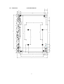
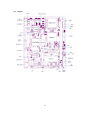
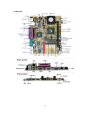
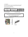
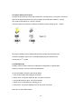
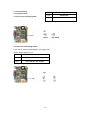
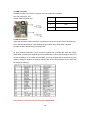
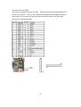
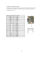
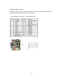
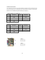
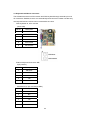
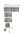
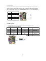
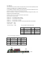
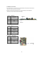
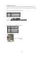
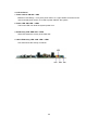
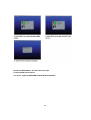
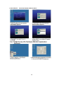
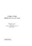
CV860A
133MHz FSB / VGA / LAN / Sound
133MHz FSB . All-in-one
Sound . 3LAN
ATA 33/66/100 . DOC . USB . IrDA . CF
Multimedia Board
NO.CV860A
Release date: Aug.2.2002
Copyright
This manual is copyrighted and all rights are reserved. It does not allow any non
authorization in copied, photocopied, translated or reproduced to any electronic or
machine readable form in whole or in part without prior written consent from the
manufacturer.
In general, the manufacturer will not be liable for any direct, indirect, special, incidental
or consequential damages arising from the use of inability to use the product or
documentation, even if advised of the possibility of such damages.
The manufacturer keeps the rights in the subject to change the contents of this
manual without prior notices in order to improve the function design, performance,
quality, and reliability. The author assumes no responsibility for any errors or omissions,
which may appear in this manual, nor does it make a commitment to update the
information contained herein.
Trademarks
Intel is a registered trademark of Intel Corporation.
Award is a registered trademark of Award Software, Inc.
All other trademarks, products and or product's name mentioned here are for
identification purposes only, and may be trademarks and/or registered trademarks
of their respective companies or owners.
© Copyright 2002
All Rights Reserved.
User Manual edition 0.1, Aug . 2 . 2002
Contents
CV860A
CHAPTER 1 GENERAL INFORMATION ........................................................................ 1
1-1 MAJOR FEATURE........................................................................................................2
1-2 SPECIFICATION .......................................................................................................... 3
1-3 PACKING LIST* .........................................................................................................…4
CHAPTER 2 HARDWARE INSTALLATION .................................................................….5
2-1 UNPACKING PRECAUTION .....................................................................................…5
2-2 UNPACKING CHECKUP ...........................................................................................…6
2-3 DIMENSION .................................................................................................................7
2-4 LAYOUT .......................................................................................................................8
2-5 DIAGRAM ....................................................................................................................9
2-6 INSTALL MEMORY .................................................................................................... 10
2-7 LIST OF JUMPERS .................................................................................................... 11
2-8 JUMPER SETTING DESCRIPTION .......................................................................... 12
2-9 CMOS DATA SET ....................................................................................................... 12
2-10 JCF1 CF CARD VOLTAGE SELECT ....................................................................... 13
2-11 JCF2 CF CARD MASTER/ SLAVE SELECT ........................................................... 14
2-12 JL2 LAN1 ENABLE/ DISABLE SELECT .................................................................. 14
2-13 JL1 LAN2 ENABLE/ DISABLE SELECT .................................................................. 15
2-14 JL4 LAN3 ENABLE/ DISABLE SELECT .................................................................. 15
2-15 DISKONCHIP™ ADDRESS SETTING .......................................….........................16
CHAPTER 3 CONNECTION ..............…...........…...........................................................17
3-1 LIST OF CONNECTORS .........................................................................................… 17
3-2 FAN CONNECTOR .................................................................................................… 18
3-3 IDE CONNECTORS ................................................................................................... 18
3-4 COMPACT-FLASH MEMORY SOCKET .................................................................... 20
3-5 PARALLEL PORT CONNECTOR ............................................................................. 21
3-6 SERIAL PORT CONNECTOR..................................................................................... 22
3-7 KEYBOARD AND MOUSE CONNECTOR ..............................................................….23
3-8 USB PORT/ HEADER ............................................................................................... 24
3-9 IR CONNECTORFAST ............................................................................................... 25
3-10 VGA CONNECTOR .................................................................................................. 25
3-11 LAN PORT ................................................................................................................ 26
3-12 AUDIO PORT CONNECTOR ................................................................................... 27
3-13 DC 12V IN AND DC OUT ......................................................................................... 28
3-14 FRONT-PANEL ......................................................................................................... 29
i
CHAPTER 4
INTRODUCTION OF BIOS...................................................................... 30
4-1 ENTER SETUP .......................................................................................................... 30
4-2 GETTING HELP ......................................................................................................... 31
4-3 THE MAIN MENU ....................................................................................................... 31
4-4 STANDARD CMOS FEATURES ................................................................................ 33
4-5 ADVANCED BIOS FEATURES .................................................................................. 34
4-6 ADVANCED CHIPSET FEATURES ........................................................................... 35
4-7 INTEGRATED PERIPHERALS .................................................................................. 36
4-8 POWER MANAGEMENT SETUP .............................................................................. 37
4-8-1
POWER MANAGEMENT ..........................................................................38
4-8-2
WAKE UP EVENTS ..................................................................................38
4-8-2.1
IRQS ACTIVITY MONITORING ............................................................ 39
4-9 PNP/PCI CONFIGURATION SETUP .......................................................................… 39
4-10 PC HEALTH STATUS ............................................................................................… 40
4-11 FREQUENCY/VOLTAGE CONTROL ...................................................................…. 41
4-12 LOAD STANDARD/OPTIMIZED DEFAULTS ........................................................... 41
4-13 SET SUPERVISOR/USER PASSWORD ................................................................. 42
CHAPTER 5
DRIVER & FREE PROGRAM INSTALLATION...................................... 43
5-1 IDE INSTALL VIA IDE/AGPVXD/IRQ ROUTING/INF DRIVER .................................. 44
5-2 VGA INSTALL VIA 8601 VGA DRIVER ...................................................................... 46
5-3 SOUND
INSTALL ALC AUDIO CODEC DRIVER FOR VIA ....................................47
5-4 PC-HEALTH
INSTALL VIA HARDWARE MONITOR DRIVER ..............................49
5-5 LAN INSTALL ............................................................................................................. 50
5-6 HOW TO DISABLE ON-BOARD SOUND .................................................................. 50
5-7 HOW TO UPDATE BIOS ............................................................................................ 50
APPENDIX A: POWER CONSUMPATION TEST.............................................................. 51
APPENDIX B: BIOS SETUP FOR IDE STORAGE......................................................…...52
ii
Chapter-1
General lnformation
The CV860A is a Light form factor All-In-One Multimedia control Board. The board design
combines all necessary input and output effects interfaces, which makes itself an ideal
all-in-one control board for POS system and multimedia applications. The board is designed
with 133 MHz internal bus clock rate architecture.
The CV860A All-In-One motherboard uses VIA PLE133( VT8601A and VT82C686B) chipset,
built-in VIA Eden/ C3 EBGA CPU, VGA and Audio feature onboard and supports , built-in
multi-LAN options (3* Realtek / 2*Intel+1*Intel Giga). The board is also designed with
AC97 2.1 sound interface which provides an ideal sound adapter in any audio
application. This board offers the superb performance and PC specification in the industry.
The motherboard is fully compatible with industry standards, adding many technical
enhancements, and is fully compatible with thousands of software applications developed
for IBM PC/AT compatible computers. The control logic provides high-speed performance
for the most advanced multiuser, multitasking applications available today.
With DMA33/66/100 access of mode 4 to IDE drive interface architecture, the IDE interface
supports maximum 100 MB/sec data transfer rate to 2 pieces of IDE drive connection.
Compact Flash Reader supports IDE/ ATA interface.
A single Flash chip holds the system BIOS, and you can change the Flash BIOS by the
Utility Update. Advanced IR port also provides a faster data transmission. You can also use
the DOS version of the "DiskOnChip
" socket which supports from 8MB up to 576MB by
issuing commands from the DOS prompt without using other software
CV860A board is designed with VT8601A intergrated graphic VGA controller which provides
connection to VGA Monitor .
VGA Controller is 64-bit single cycle 2D/3D graphic engine which supports up to 1600x1200
extended screen resolutions and also real time DVD MPEG-2 and AC3 playback.
The CV860A Board supports SDRAM memory with one DIMM socket up to 512MB.
1
1-1 Major Feature
1.
VIA Eden EBGA 400/533/667MHz low power CPU/ VIA C3 EBGA 733/800 MHz CPU
2.
VIA PLE133 chipset (VT8601A + VT82C686B)
3.
One PC 133/100 SDRAM DIMM socket up to 512MB
4.
Dual channel master mode PCI support four IDE disk drives
5.
100/133MHz system clock support
6.
Versatile storage device:
*
One 50-pin Compact Flash socket
*
One 32-pin DOC socket
*
One 40-pin DOM
*
One 44-pin DOM
*
One 2.5" HDD
DMA 33/66/100 controller
7.
On board VT8601A graphic controller integrated Trident graphics
8.
On board multi-LAN option*:
9.
*
CV860A-1R ----1* Realtek 8100B 10/100B-T
*
CV860A-3R ----3* Realtek 8100B 10/100B-T
*
CV860A-1T ----1* Intel 82551 10/100B-T
*
CV860A-3U ----2* Intel 82551 10/100B-T + 1* Intel 82540 EM 10/100/1000B-T LAN
DiskOnChip memory size 8MB up to 576MB
10. Compact Flash Reader Type I/II for IDE/ATA interface
11. Two serial RS232 Ports
12. Two enhanced bi-directional parallel ports (SPP/ECP/EPP)
13. On board mini PS/2 Keyboard/Mouse connector
14. On board Sound ALC 201A, AC97 2.1
15. DC 12V-IN Power Adapter support
*The models mentioned above are standard models currently.
The multi-LAN option might change due to customization.
2
1-2 Specification
1.CPU: VIA C3 EBGA 400/533/ 667 MHz low power CPU / VIA C3 EBGA 733/800 MHz CPU
2. Cache Memory: Intergrated full-speed 192KB L1/L2 cache
3.Chipset: VIA PLE133 (North:VT8601A ;South:VT82C686B)
4. Memory: One DIMM socket up to 512MB SDRAM
5. VGA: VT8601A integrated graphic controller ; support 64-bit 2D/3D display up to
1600x1200, memory sharable up to 8MB
6. I/O Chipset: VIA VT82C686B
7. IDE: four IDE disk drives; support DMA33/66/100 transfer rate up to 33/66/100 MB/sec
8. LAN:
* CV860A-1R ----1* Realtek 8100B 10/100B-T (Wake-On-LAN)
* CV860A-3R ----3* Realtek 8100B 10/100B-T (Wake-On-LAN)
* C860A-1T ----1* Intel 82551 10/100B-T
* CV860A-3U ----2* Intel 82551 10/100B-T + 1* Intel 82540 EM
10/100/1000B-T LAN
9. Storage devices: * One 50-pin Compact Flash socket
* One 32-pin DOC socket
* One 40-pin DOM
* One 44-pin DOM
* One 2.5" HDD
10. DiskOnChip: 32-pin socket for DiskOnChip DOC2000 ; memory size from 8MB to 576MB
11. Parallel Port: 1 parallel port ; Support SPP/ECP/EPP
12. Serial Port: Two serial ports ; Support RS-232
13. IR: One IrDA TX/RX header
14. USB: Support four USB ports
15. Keyboard: PS/2 6-pin Mini Din
16. Mouse: PS/2 6-pin Mini Din
17. Sound: AC97 2.1 Sound, full-duplex
18. BIOS: Award BIOS version 6.1
19. Form Factor: LIGHT Board, 200x150mm
20. Power: DC12V-IN power Adapter input
21. Power Voltage: +12V (11.4V to 12.6V)
3
1-3 Packing List*
1 CV860A Board
6 Utility CD Disk
2 DC 12V Power Adapter
7 User's Manual
3 One ATA 100 Flat Cable (2.54mm)
4 One slim IDE port flat Cable (2.00mm)
5 Power Cable
3
2
4
1
7
5
6
*The packing list above is for the users who purchase single motherboard. The users
who purchase the board with chassis may refer to the packing list in the Assembly Guide.
Please contact with your dealer if any of these items is missing or damaged
on delivery. And please keep all parts of the delivery package with packing
materials in case if you need to deliver or store the product in the future.
4
Chapter-2
Hardware Installation
This chapter provides the information how to install the hardware of CV860A.
Please follow section 1.3, 2.1 and 2.2 to check the delivery package and unpack
carefully. Please follow the jumper setting procedure.
2-1 Unpacking Precaution
The CV860A board has been well packed with an anti-static bag to protect its
sensitive components and circuitry from the damage of static electric discharge.
Note: DO NOT TOUCH THE BOARD OR ANY OTHER SENSITIVE COMPONENTS
WITHOUT ALL NECESSARY ANTI-STATIC PROTECTION.
You should follow these
steps to protect the board from the static electric
discharge whenever you handle the board:
1. Ground yourself by a grounded wrist strap at all times when you handle the CV860A.
Well clip the ALLIGATOR clip of the strap to the end of the shielded wire lead from
a grounded object. Please put on and connect the strap before handling the CV860A
for harmlessly discharge any static electricity through the strap.
2. Please use anti-static pad to put any components, parts, or tools on the pad whenever
you work on them outside the computer. You may also use the anti-static bag instead of
the pad. Please ask your local supplier for necessary parts on anti-static requirement.
3. Do not plug any connector or set any jumper when the power is on.
5
2-2 Unpacking checkup
First of all, please follow all necessary steps of section 2.1 to protect CV860A
from electricity discharge. With reference to section 1.3, please check the delivery package
again with following steps:
1. Unpack the CV860A board and keep well storage of all packing material, manual
and driver disc etc.
2. Is there any components lose or drop from the board? DO NOT INSTALL IF
HAPPENED.
3. Is there any visible damage on of the board? DO NOT INSTALL IF HAPPENED.
4. Well check your optional parts (i.e. SRAM, DOC etc.), all necessary jumpers
setting to jumper pin-set, and CMOS setup correctly.
Please also refer to all information of jumper settings in this manual.
5. Well check your external devices (i.e. Add-On-Card, Driver Type etc.)
for complete add-in or connection and CMOS setup correctly.
Please also refer to all information of connector connection in this manual.
6. Please keep all necessary manual and driver disc in a good condition for your
necessary re-installation if you change your Operating System.
6
2-3 Dimension
Light 200x150(mm)
7
2-4 Layout
8
2-5 Diagram
9
2-6 Install Memory
This motherboard provides one 168-pin DUAL INLINE MEMORY MODULES (DIMM)
socket for memory expansion available from minimum memory size over 32MB to
maximum memory size of 512MB SDRAM.
Mixed 1M/2M/4M/8M/16M/32M x N DRAMs Type.
Valid Memory Configurations
Dimm1
System Accept or Not
Total Memory
Min.~ Max
DS/SS
Accept
DS: Double Sided DIMM
32MB~512MB
SS: Single Sided DIMM
NOTE!
Make sure the total installed memory does not exceed 512MB;
otherwise, the system may hang during startup.
The maximum height of DIMM is 30mm.
Install SDRAM module oriented as Fig. 2.1.
10
NOTE!
When you install DIMM module fully into the DIMM socket, the eject tab should be
locked into the DIMM module very firmly and fit into its indention on both sides.
WARNING!
If the SDRAM CLOCK is set at 133MHz, you must use PC133-compliant
DIMMs. When this motherboard operates at 133Mhz, most system will not even
boot if non PC133-compliant SDRAM modules are used because of
the strict timing issues. If your DIMMs are not PC133-compliant, set the SDRAM
clock at 100MHz to ensure system's stability.
2-7 List of Jumpers
JB1: CMOS DATA SET
JCF1: CF Card Voltage select
JCF2: CF Card Marster/Slave select
JD1: DiskOnChip address select
JL2: LAN1 Enabled/Disabled select
JL1: LAN2 Enabled/Disabled select
JL4: LAN3 Enabled/Disabled select
11
2-8 Jumper Setting Description
A jumper is ON as a short circuit with a plastic cap covering two pins. A jumper is OFF as an
open circuit without the plastic cap. Some jumpers have three pins, labeled 1, 2, and 3.
You could connect either pin 1 and 2 or 2 and 3.
The below figure 2.2 shows the examples of different jumper settings in this manual.
All jumpers already have its default setting with the plastic cap inserted as ON,
or without the plastic cap as OFF. The default setting may be referred in this
manual with a " * " symbol .
2-9 CMOS Data Set
A battery must be used to retain the motherboard configuration in CMOS RAM.
Close pin 1and pin 2 of JB1 to store the CMOS data.
To clear the CMOS, follow the procedures below:
1. Turn off the system and unplug the AC power
2. Remove DC 12V power cable from DC 12V power connector
3. Locate JB1 and short pin 2-3 for a few seconds
4. Return to its normal setting by shorting pin 1-2
5. Connect DC 12V power cable back to DC 12V power connector
Note: Do not clear CMOS unless
12
1. Troubleshooting
2. Forget password
3. You fail over-clocking system
JB1
Description
*1-2
*Normal Set
2-3
CMOS Data clear
2-10 JCF1 CF Card Voltage select
If you use CF card and HDD together, we suggest you
use the jumper setup for +5V.
JCF1
Description
1-2
CF Card use 3.3 Voltage
*2-3
*CF Card use +5V voltage
13
2-11 JCF2 CF Card Master/Slave select
If you use CF card and HDD together, please set CF as Master and HDD as Slave.
JCF2
Description
1-2
CF Card use Salve type
*2-3
*CF Card use Master type
2-12 JL2 LAN1 Enable/Disable select
CV860A can be quipped with three built-in Ethernet controller at most. You can enable/
disable the LAN function of each RJ-45 jack by the following setup.
JL2
Description
*1-2
LAN1 Hardware set Enabled
2-3
LAN1 Hardware set Disabled
14
2-13 JL1 LAN2 Enable/Disable select
JL1
Description
*1-2
* LAN2 Hardware set Enabled
2-3
LAN2 Hardware set Disabled
2-14 JL4 LAN3 Enable/Disable select
JL4
Description
*1-2
* LAN3 Hardware set Enabled
2-3
LAN3 Hardware set Disabled
15
2-15 DiskOnChip™ Address Setting
The CV860A provides a socket to install the DiskOnChip™ module.
DOC 32-pin dip socket can support flash disk up to 576MB
There are three DOC address setting options:
D000-D1FFh ,D800-D9FFh,DC00h-DDFFh,DE00-DFFFh.
A JD1 may select the starting memory address of the DiskOnChip™ (D.O.C.) to avoid the
mapping area with any other memory device. If you have other memory device in the
system, please set both at different memory address mapping.
JD1
Description
*1-2
* D000h-D1FFh
3-4
D800h-D9FFh
5-6
DE00h-DFFFh
The D.O.C. function allows the system to operate without FDD or HDD. The D.O.C. may be
format as driver C: or driver A:. User may also use the DOS commands such as FORMAT,
SYS, COPY, XCOPY, DISCOPY and DISKCOMP etc. This means that the D.O.C. may
be used as driver-A if the system works without FDD-A for ambient application.
Please contact with your supplier for different size of D.O.C. module. You can find the latest
information on www.m-sys.com .
16
Chapter-3
Connection
This chapter provides all necessary information of the peripheral's connections,
switches and indicators. Always power off the board before you install the peripherals.
3-1 List of Connectors
CN4: DC 12V in power Jack
CN9: DC output for +5/+12V Connector
J2 : Dual PS2 6-pin Mini Din Keyboard and Mouse Jack
JKB: External Keyboard Connector
J1 : USB 1/2 and RJ45(LAN2) Jack
J4 : COM1 DB9 Connector
CN5: Parallel Port 1 DB25 Connector
CN3: VGA DB15 Connector
J3 : COM2 DB9 Connector
CN2: RJ45 LAN1 Jack
CN1: RJ45 LAN3 Jack
IDE1: IDE1 2x20 Pin(2.54mm) Connector
CN6: IDE2 2x22 Pin (2.0mm) Connector
CN7: CF Card 50-pin Socket
U14: DiskOnChip Socket
JI1: IR Connector
J5 : USB 4 Port Jack
JUSB: USB 3 Port Connector
J6 : MIC-IN Jack
J5 : LINE - OUT Jack
J9 : CD Audio In Jack
JF2: System FAN connector
LED1 : LAN Active LED
LED2 : HDD Active LED
LED3 : Power Active LED
SW1 : Power on switch
JF3: CPU FAN Connector
17
3-2 FAN Connector
CV860A provides one CPU fan connector and one system fan connector.
CPU Fan Connector- JF3
System FAN Connector-JF2
PIN NO.
Description
1
FAN Control ON/OFF
2
+12V
3
FAN speed Sensor
3-3 IDE Connectors
There are two kinds of IDE connectors on this board, 40-pin and 44-pin. Each can support up
to two IDE-inferface devices. One standard 40-pin header daisy-chain driver connector
provides as IDE1 with following pin assignment.
40 pins (2.54mm)-IDE1(IDE 1)This connector supports the provided IDE hard disk ribbon
cable. After connecting the single plug end to motherboard, connect the two plugs at other end
to your hard disk(s). If you install two hard disks, you must configure the second drive as Slave
mode by setting its jumpers accordingly. Please refer to the documentation of your hard disk
for the jumper settings.
Note: Pin20 is +5V power can use new type DOM module.
18
44 pins(2.0mm)-CN2 (IDE2)
This connector supports slim type 2.5" HDD. Follow the same procedure described for the
primary IDE connector. You may also configure two hard disks as both Masters using one
ribbon cable on the primary IDE connector and another ribbon cable on the secondary
IDE connector. (See Appendix B)
19
3-4 Compact - Flash Memory Socket
CV860A configures CompactFlash Storage Card in IDE mode. It will use IDE channel when
CompactFlash card is plugged in. This socket supports CF Card Type I/II socket spec.
CF Socket 50pin----CN7
20
3-5 Parallel Port Connector
Parallel Port connector is a D-type 25-pin female connector. The On-board Parallel Port can
be disabled through the BIOS SETUP (see Chapter 4)
. CN5: Parallel Port Connector ---CN5 D-SUB 25 PIN
21
3-6 Serial Port Connector
The CV860A board offers two high speed NSI6C550 compatible UARTS with Read/ Receive
16 byte FIFO serial ports. The serial ports are two DB-9 external connectors. The On-board
serial port can be disabled through BIOS SETUP (see Chapter 4).
. COM1 Connector - J4 D-SUB 9-Pin
PIN NO.
Description
PIN NO.
Description
1
DCD
6
DSR
2
RXD
7
RTS
3
TXD
8
CTS
4
DTR
9
5
GND
RI
. COM2 Connector-J3 D-SUB 9-pin
PIN NO.
Description
PIN NO.
Description
1
DCD
6
DSR
2
RXD
7
RTS
3
TXD
8
CTS
4
DTR
9
RI
5
GND
22
3-7 Keyboard and Mouse Connector
The CV860A lets users use PS/2 mouse and PS/2 keyboard through external 6-pin mini
din connectors. Besides, there is one external keyboard connector. Please note that only
one keyboard and one mouse can be connected at one time.
.
PS2 Keyboard-J2, 6-Pin mini din
(down side)
.
PIN NO.
Description
1
KB DATA
2
MS DATA
3
GND
4
+5V
5
KB CLOCK
6
MS CLOCK
External Keyboard Connector-JKB,
5pin(2.54mm)
.
PIN NO.
Description
1
KB DATA
2
KEY
3
GND
4
+5V
5
KB CLOCK
PS2 Mouse-J2, 6pin mini din(Up Side)
PIN NO.
Description
1
MS DATA
2
NC
3
GND
4
+5V
5
MS CLOCK
6
NC
23
3-8 USB Port/ Header
The CV860A provides three external 4-pin Jacks for USB-1/2 and USB-4 as well as
one 4-pin header for USB-3. Please refer to the following default pin assignment.
.
.
.
USB 1/2 Port Connector-J1
PIN NO.
Description
PIN NO.
Description
1
+5V
1
+5V
2
USB DATA0-
2
USB DATA1-
3
USB DATA0+
3
USB DATA1+
4
GND
4
GND
USB 4 Port Connector-J5
PIN NO.
Description
1
+5V
2
USB DATA3-
3
USB DATA3+
4
GND
USB 3 Header-JUSB
PIN NO.
Description
1
+5V
2
USB DATA2-
3
USB DATA2+
4
GND
24
3-9 IR Connector
This built-in IR connector supports the optional wireless transmitting and receiving infrared
module. It supports Infra-red Data Association (IrDA) and Amplitude Shift Keyed IR (ASKIR).
You can configure the setting through the BIOS setup to use the IR function. (see Chapter 4)
.
IR Connector -JI1 5-pin(2.54mm)
PIN NO.
1
Description
+5V
2
KEY
3
IRRX
4
GND
5
IRTX
3-10 VGA Connector
The CV860A provides one D-type 15-pin connector for the CRT VGA monitor.
.
VGA DB15 Connector: CN3 DB15-pin
PIN NO.
Description
PIN NO.
Description
PIN NO.
Description
1
RED
6
GND
11
NC
2
GREEN
7
GND
12
DDC DATA
3
BULE
8
GND
13
H-SYNC
4
NC
9
NC
14
V-SYNC
5
GND
10
GND
15
DDC CLOCK
25
3-11 LAN Port
The Fast Ethernet controller provides 32-bit performance, PCI bus master capability, and full
compliance with IEEE 802.3u 10/100Based-T specification.
For 10/100Base-T operation, please connect the network connection by plugging one end of
the cable into the RJ-45 jack of the CN2/J1/CN1 Connector.
Besides 10/100 Base-T, CV860A can provide Giga LAN solution through CN1 (LAN 3), once
equipped with Intel 82540EM chipset.
CV860A provides multi-LAN solution with various chip and spec.
Here is the list of current models:
CV860A-1R ---- One Realtek 8100B 10/100B-T
CV860A-3R ---- Three Realtek 8100B 10/100B-T
CV860A-1T ---- One Intel 82551 10/100B-T
CV860A-3U ---- Two Intel 82551 10/100B-T and One Intel 82540 EM 10/100/1000B-T
CN2 RJ45 JACK-----LAN1
J1 RJ45 JACK------- LAN2
CN1 RJ45 JACK-----LAN3
. RJ-45 10/100B-T JACK-CN2/J1/CN3
PIN NO.
Description
PIN NO.
Description
1
TX+
5
NC
2
TX-
6
RX-
3
RX+
7
NC
4
NC
8
NC
. RJ-45 10/100/1000B-T JACK-CN3
PIN NO.
Description
PIN NO.
Description
1
MID0+(TX+)
5
MID2-
2
MID0-(TX-)
6
MID1-(RX-)
3
MID1+(RX+)
7
MID3+
4
MID2-
8
MID3-
26
3-12 Audio Port Connector
The CV860A has an on-board AC'97 3D sound interface. There are the connectors of
LINE OUT, MIC-IN and CD-IN connectors.
The MIC-IN Jack and CD-IN header are for audio sound input. The LINE-OUT
connector is a 4-pin Jack for audio sound output.
J7 Jack-----LINE-OUT
PIN NO.
Description
1
+5V
2
KEY
3
IRRX
4
GND
5
IRTX
J6 Jack-----MIC-IN
PIN NO.
1
Description
GND
2
MIC-IN
3
GND
4
NC
5
MIC-POWER
J9 Connector-----CD Audio-in
PIN NO.
1
Description
CD-L
2
GND
3
GND
4
CD-R
27
3-13 DC 12V IN and DC out
The CV860A uses single +12V power input and provides DC output header for devices.
When you plug the device's power cable into the power header, please note the orientation.
CN4 ----- DC 12V IN for 2.54mm Power connector
PIN NO.
Description
1,2,4
GND
3
+12V IN
CN9 ----DC OUT for 2.54 mm Power connector
PIN NO.
Description
1
+5V
2
GND
3
GND
4
+12V
28
3-14 Front-Panel
1. Power switch: PW-ON--- SW1
Based on case design , it may be a power switch or a 2-pin header connected to the
case-mounted power switch. It is used to power ON/OFF the system.
2. Power LED: PW-LED ---LED3
The Power LED is lit while the system power is on.
3. IDE Activity LED: HDD-LED---LED2
HDD-LED shows the activity of the hard disk.
4. LAN LED Activity LED: LAN- LED----LED1
LAN LED shows the activity of network.
29
Chapter 4
Introduction of BIOS
The BIOS is a program located in the Flash Memory on the motherboard.
This program is a bridge between motherboard and operating system.
When you start the computer, the BIOS program gains control. The BIOS first
operates an auto-diagnostic test called POST (Power on Self Test) for all the
necessary hardware, it detects the entire hardware devices and configures the
parameters of the hardware synchronization. After these tasks are completed,
BIOS will give control of the computer back to operating system (OS). Since the BIOS
is the only channel for hardware and software to communicate with, it is the key factor
of system stability and of ensuring your system performance at best.
In the BIOS Setup main menu of Figure 3-1, you can see several options. We will
explain these options in the following pages. First, let us see the function keys
you may use here:
. Press <Esc> to quit the BIOS Setup.
. Press ↑↓←→ (up, down, left, right) to choose the option you want to confirm or modify.
. Press <F10> to save these parameters and to exit the BIOS Setup menu after
you complet the setup of BIOS parameters.
. Press Page Up/Page Down or +/- keys to modify the BIOS
parameters for the active option.
4-1 Enter Setup
Power on the computer and press <Del> immediately to enter Setup.
If the message disappears before your respond but you still wish to enter Setup,
restart the system by turning it OFF then ON button on the system case. You may
also restart the system by simultaneously pressing <Ctrl>, <Alt> and <Delete> keys.
If you do not press the keys at the proper time and the system does not boot, an
error message will display and you will be asked to
Press <F1> to continue, <Ctrl-Alt-Esc> or <Del> to enter Setup
30
4-2 Getting Help
Main Menu
The on-line description of the highlighted setup function is displayed at the
bottom of the screen.
Status Page Setup Menu/ Option Page Setup Menu
Press F1 to pop up a small help window that describes the appropriate keys to use
and the possible selections for the highlighted item.
To exit the Help Window, press <Esc>.
4-3 The Main Menu
Once you enter Award BIOS CMOS Setup Utility, the Main Menu will appear on the
screen. The Main Menu has fourteen setup functions and two exit choices.
Use arrow keys to select among these items. Press <Enter> to accept or enter
the sub-menu.
31
Standard CMOS Features
This Menu is for basic system configurations.
Advanced BIOS Features
This menu is to set the Advanced Features available in your system.
Advanced Chipset Features
This menu is to change the values in the chipset registers and optimize your
system performance.
Integrated Peripherals
This menu is to specify your settings for integrated peripherals.
Power Management Setup
This menu is to specify your settings for power management.
PnP/PCI configurations
This entry appears if your system supports PnP/PCI.
PC Health Status
This entry shows your PC health status.
Frequency/Voltage Control
This menu is to specify your settings for Miscellaneous Control.
Load Optimized Defaults
Use this menu to load the BIOS default values that are factory settings for optimal
system operation performance. It is provided for the skillful users who want to
push the motherboard to get better performance. The Optimized setting does not go
through all the reliability and compatibility tests, it is verified only with limited
configurations and loading (for example, a system that is equipped with only one VGA
card and one DIMM. Do not use Optimized setting unless you fully understand the
items in chipset setup menu.
32
Load Standard Defaults
Use this menu to load the BIOS default values for the optimum system performance.
Standard Defaults settings are relatively more reliable than Optimized Defaults.
All the product verifications, compatibility test reports and manufacture quality
controls are based on "Standard Defaults". We suggest you to use this setting
for normal operation. "Standard Defaults" is not the slowest setting for this
motherboard. If you need to verify an unstable problem, you may manually set the
parameter in "Advanced Chipset Features" to get slower and safer setting.
Set Supervisor/User Password
This menu is to set User and Supervisor Passwords.
Save & Exit Setup
Save CMOS values modified to CMOS and exit setup.
Exit Without Saving
Abandon all the CMOS values modified and exit setup.
4-4 Standard CMOS Features
The items in Standard CMOS Setup Menu are divided into several categories.
Each category includes no, one or more than one setup items. Use the arrow
keys to highlight the item and then use the <PgUp> or <PgDn> keys to select
the value you want to modify with this item.
33
4-5 Advanced BIOS Features
Virus Warning
The VIRUS Warning feature can help you protect IDE Hard Disk boot sector.
If this function is enabled, BIOS will show a warning message on screen and alarm
beep when somenoe attemps to write data into this area without permission.
Disabled (default) No warning message appears when anything attempts to
access the boot sector or hard disk partition table.
Enabled Activate automatically when the system boots up. The system
will show the warning message if anything attempts to
access the boot sector of hard disk partition table.
34
4-6 Advanced Chipset Features
The Advanced Chipset Features Setup option is used to change the values of the
chipset registers. These registers control most of the system options in the computer.
The "Advanced DRAM Control" includes settings for the chipset dependents features.
These features are related to system performance. Make sure you fully understand
the items contained in this menu before you change anything. You may
change the parameter settings to improve system performance. However, it may
make your system unstable if the setting is not correct for your system configuration.
PCI Delay Transaction
The chipset has an embedded 32-bit posted write buffer to support delay
transactions cycles. Select Enabled to support compliance with PCI specification
version 2.1. The settings are Enabled or Disabled.
35
4-7 Integrated Peripherals
Note: If you find conflicts on IRQ Address, please adjust I/O port IRQ address setting.
Init Display First
36
4-8 Power Management Setup
The Power Management Setup allows you to configure your system to most
effectively save energy saving while operating in a manner consistent with your
own style of computer use.
Wake-Up Events
Please refer to section 4-8-2
37
4-8-1
Power Management
4-8-2
Wake Up Events
IRQs Activity Monitoring
Please refer to section 4-8-2.1
38
4-8-2.1
IRQs Activity Monitoring
4-9 PnP/PCI Configuration Setup
This section describes how to configure the PCI bus system. PCI, or Personal Computer
Interconnect, is a system which allows I/O devices to operate at the speed the CPU itself
keeps when CPU communicates with its own special components. This section covers
some very technical items and we strongly recommended that only experienced users
should make any change to the default settings.
39
Resource Controlled By
The Award Plug and Play BIOS can automatically configure all of the boot and Plug
and Play compatible devices. However, this capability means absolutely nothing unless
you are using a Plug and Play operating system such as Windows 95/98. If you set
this field to "manual", choose a specific resource by going into each sub menu that
follows this field (a sub menu is preceded by a ">").
The settings are Auto (ESCD) or Manual.
IRQ Resources
When resources are controlled manually, each system interrupt is assigned a type,
depending on the type of device using the interrupt.
PCI/VGA Palette Snoop
Leave this field at Disabled. The settings are Enabled or Disabled.
4-10 PC Health Status
This section shows the status of your CPU, Fan, and overall system.
This is only available when there is Hardware Monitor function onboard.
Show PC Health in Post
During Enabled, it displays information list below. The choice is either
Enabled or Disabled
Current CPU Temperature/Current System Temp/Current FAN1,FAN2 Speed/
Vcore/2.5V/3.3V/+5V/+12V
This will show the CPU/FAN/System voltage chart and FAN Speed
40
4-11 Frequency/Voltage Control
This section is to set CPU Frequency Control.
Auto Detect DIMM/PCI Clock
This item allows you to enable or disable Auto Detect DIMM/PCI Clock.
The settings are Enabled or Disabled.
Spread Spectrum
This item allows you to set the CPU Host/PCI clock Spread Spectrum.
The choice are Disabled or Enabled.
4-12 Load Standard/Optimized Defaults
Load Standard Defaults
When you press <Enter> on this item, you get confirmation dialog box with a
message similar to:
Load Standard Defaults (Y/N)? N
Press <Y> to load the BIOS default values for the most stable system operation and
minimal performance.
Load Optimized Defaults
When you press <Enter> on this item, you get a confirmation dialog box with a
message similar to:
Load Optimized Defaults (Y/N)? N
Press <Y> to load the default values that are factory settings for optimal
system operation performance.
41
4-13 Set Supervisor/ User Password
You can set supervisor password, user password, or both. The differences are:
Supervisor password: You can enter the setup menus and change the options.
User password:
You can enter the setup menus but do not have the right to
change the options. When you select this function, the
following message will appear at the center of the screen to
assist you in creating a password.
ENTER PASSWORD:
Type the password, up to eight characters in length, and press <Enter>. The password
typed will clear any previous password from CMOS memory. You will be
asked to confirm the password. Type the password again and press <Enter>. You may
also press <Esc> to abort the selection without entering password.
To disable a password, just press <Enter> when you are prompted to enter the
password. A message will confirm if you want to disable the password. Once the
password is disabled, the system will boot and you can enter Setup menus freely.
PASSWORD DISABLED.
When a password has been enabled, you have to enter it every time before you
enter the Setup. This prevents an unauthorized person from changing any part of
your system configuration.
Additionally, when a password is enabled, you can also have the BIOS to request a
password at every time when your system is rebooted. This would prevent the
unauthorized user.
You can determine if the password is required within the BIOS Features Setup Menu
and its Security option. If the Security option is set to "System", the password will
be required both at boot and at entry to Setup. If set to "Setup",
the password is required only at the entry to Setup.
42
Chapter5
DRIVER & FREE PROGRAM INSTALLATION
There is a SYSTEM INSTALL CD disk in the package. This CD has all the drivers you
need and some free application programs and utility programs. In addition, this CD also
includes an auto-detect software which can tell you which hardware is installed and
which driver is needed so that your system can function properly.
We call this auto detect software SYSTEM INSTALL.
SYSTEM INSTALL Supports WINDOWS
95/98/98SE/ME/NT4.0/2000/XP
Insert the CD into your CD-ROM drive and the SYSTEM INSTALL Menu should appear as
below. If the menu does not appear, double-click MY COMPUTER and double-click
CD-ROM drive or click START, click RUN, and type X:\SETUP.EXE (assuming X is your
CD-ROM drive).
From SYSTEM INSTALL MENU you may make 3 selections:
1 . Auto detect main board and OS Into auto install driver Menu
2 . Explore CD to explore the contents of the CD
3. EXIT to exit from SYSTEM INSTALL menu
43
Auto install driver Menu
1. IDE
install VIA IDE/AGPVXD/IRQ ROUTING/INF driver
2. VGA
install on-board VGA driver
3. SOUND
install AC97 Audio Codec Installing driver
4. PC-HEALTH
install VIA PC-HEALTH hardware monitor driver
5. LAN
to LAN install driver readme file
6. DIRECTX
install DirectxX driver
Each selection is illustrated as below:
5-1 IDE
Install VIA IDE/AGPVXD/IRQ ROUTING/INF Driver
IDE :
VIA ATAPI VENDOR SUPPORT DRIVER IS USED TO FIX
COMPATIBILITY ISSUE FOR IDE DEVICES.
AGP VXD :
VIA AGP VXD DRIVER IS TO BE INSTALLED. IF YOU ARE USING
AN AGP VGA CARD, VIAGART.VXD WILL PROVIDE SERVICE
ROUTINES TO YOUR VGA DRIVER AND INTERFACE DIRECTLY
TO HARDWARE, PROVIDING FAST GRAPHIC ACCESS.
IRQ ROUTING :
VIA PCI IRQ MINIPORT DRIVER IS TO BE INSTALLED UNDER WIN98
ONLY. IT WILL FIX PCI IRQ ROUTING SEQUENCE.
INF :
VIA REGISTRY DRIVER IS TO BE INSTALLED UNDER WINDOWS.
THE DRIVER WILL ENABLE VIA POWER MANAGERMENT
CONTROLLER.
44
45
NOTE: SYSTEM INSTALL will auto detect file path
X:\driver\VIA\Driver\setup.exe
This driver supports WINDOWS 95\98\98SE\NT4.0\2000\XP
46
5-2 VGA
INSTALL VIA 8601 VGA Driver
NOTE: The path of the file For WINDOWS 95/98/98SE\ME
X:\driver\VIA\8601VGA\WIN9Xme\SETUP.EXE
For NT4.0
X:\driver\VIA\8601VGA\NT40
For WINDOWS 2000
X:\driver\VIA\8601VGA\W2kxp\SETUP.EXE
47
5-3 SOUND
Install ALC Audio Codec Driver for VIA
NOTE: The path of the file For WIN98/NT4.0/WIN2K \XP
X:\ driver\via\viaudio\setup.exe
48
5-4 PC-HEALTH
Install VIA Hardware Monitor Driver
49
5-5
HOW TO DISABLE ON-BOARD SOUND
Enter BIOS SETUP. Choose INTEGRATE PERIPHERALS. Choose ON-CHIP DEVICE
FUNCTION. Choose AC97 AUDIO Disable on-board sound function by pressing
PAGE DOWN KEY to Disable.
5-6
HOW TO UPDATE BIOS
Method 1.
Use "Magic BIOS" to update BIOS in Windows 98 (refer to page 40)
Method 2.
In DOS Mode
STEP 1. Prepare a boot disc. (you may make one by clicking START, clicking RUN,
typing SYS A:
, and clicking OK)
STEP 2. Copy utility program to your boot disc. You may copy it from DRIVER CD
X:\FLASH\AWDFLASH.EXE or download it from our web site.
STEP 3. Copy the latest BIOS for CV860A from our web site
to your boot disc.
STEP 4. Insert your boot disc into A:
Start the computer and type "Awdflash A:\CV860Axxx.BIN/SN/PY/CC/R"
CV860Axxx.BIN is the file name of the latest BIOS. It may be CV860AA1.
BIN or CV860AB2.BIN
SN
means
don't save the current BIOS data
PY
means
renew the current BIOS data
CC
means
clear the current CMOS data
R
means
restart computer
STEP 5. Press ENTER and the BIOS will be updated,
computer will restart automatically.
50
Appendix A: Power Consumption Test
Condition
Item
Spec
CPU
VIA Eden 533MHz -- on board
DRAM
256MB SDRAM (KingStone)
VGA
VT8601A (1024*768*32) - on chip
Storage Driver
CF 64MB (Toshiba); DOC 16MB (M-System)
BIOS
Award Optimal default
Operating System.
Windows ME
Test Program
3D Mark 2000
Test Result
Hard Disk
Max.
Operating
Static
Slim Type HDD
1.81A/ 12V
1.5A/ 12V
0.08A
Standard HDD
2.18A/ 12V
1.8A/ 12V
0.08A
51
Appendix B: BIOS Setup for IDE Storage
52
53