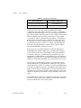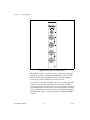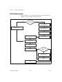
1
DAQ
NI PXI-4461 User Manual
Dynamic Signal Acquisition Device
for PXI/CompactPCI
NI PXI-4461 User Manual
March 2004 Edition
Part Number 373088A-01
Support
Worldwide Technical Support and Product Information
ni.com
National Instruments Corporate Headquarters
11500 North Mopac Expressway
Austin, Texas 78759-3504 USA Tel: 512 683 0100
Worldwide Offices
Australia 1800 300 800, Austria 43 0 662 45 79 90 0, Belgium 32 0 2 757 00 20, Brazil 55 11 3262 3599,
Canada (Calgary) 403 274 9391, Canada (Ottawa) 613 233 5949, Canada (Québec) 450 510 3055,
Canada (Toronto) 905 785 0085, Canada (Vancouver) 514 685 7530, China 86 21 6555 7838,
Czech Republic 420 224 235 774, Denmark 45 45 76 26 00, Finland 385 0 9 725 725 11,
France 33 0 1 48 14 24 24, Germany 49 0 89 741 31 30, Greece 30 2 10 42 96 427, India 91 80 51190000,
Israel 972 0 3 6393737, Italy 39 02 413091, Japan 81 3 5472 2970, Korea 82 02 3451 3400,
Malaysia 603 9131 0918, Mexico 001 800 010 0793, Netherlands 31 0 348 433 466,
New Zealand 0800 553 322, Norway 47 0 66 90 76 60, Poland 48 22 3390150, Portugal 351 210 311 210,
Russia 7 095 783 68 51, Singapore 65 6226 5886, Slovenia 386 3 425 4200, South Africa 27 0 11 805 8197,
Spain 34 91 640 0085, Sweden 46 0 8 587 895 00, Switzerland 41 56 200 51 51, Taiwan 886 2 2528 7227,
Thailand 662 992 7519, United Kingdom 44 0 1635 523545
For further support information, refer to the Technical Support and Professional Services appendix. To comment
on the documentation, send email to [email protected].
© 2004 National Instruments Corporation. All rights reserved.
Important Information
Warranty
The NI PXI-4461 is warranted against defects in materials and workmanship for a period of one year from the date of shipment, as evidenced
by receipts or other documentation. National Instruments will, at its option, repair or replace equipment that proves to be defective during the
warranty period. This warranty includes parts and labor.
The media on which you receive National Instruments software are warranted not to fail to execute programming instructions, due to defects
in materials and workmanship, for a period of 90 days from date of shipment, as evidenced by receipts or other documentation. National
Instruments will, at its option, repair or replace software media that do not execute programming instructions if National Instruments receives
notice of such defects during the warranty period. National Instruments does not warrant that the operation of the software shall be
uninterrupted or error free.
A Return Material Authorization (RMA) number must be obtained from the factory and clearly marked on the outside of the package before
any equipment will be accepted for warranty work. National Instruments will pay the shipping costs of returning to the owner parts which are
covered by warranty.
National Instruments believes that the information in this document is accurate. The document has been carefully reviewed for technical
accuracy. In the event that technical or typographical errors exist, National Instruments reserves the right to make changes to subsequent
editions of this document without prior notice to holders of this edition. The reader should consult National Instruments if errors are suspected.
In no event shall National Instruments be liable for any damages arising out of or related to this document or the information contained in it.
EXCEPT AS SPECIFIED HEREIN, NATIONAL INSTRUMENTS MAKES NO WARRANTIES , EXPRESS OR IMPLIED, AND SPECIFICALLY DISCLAIMS ANY WARRANTY OF
MERCHANTABILITY OR FITNESS FOR A PARTICULAR PURPOSE . C USTOMER’S RIGHT TO RECOVER DAMAGES CAUSED BY FAULT OR NEGLIGENCE ON THE PART OF
NATIONAL INSTRUMENTS SHALL BE LIMITED TO THE AMOUNT THERETOFORE PAID BY THE CUSTOMER. NATIONAL INSTRUMENTS WILL NOT BE LIABLE FOR
DAMAGES RESULTING FROM LOSS OF DATA, PROFITS, USE OF PRODUCTS, OR INCIDENTAL OR CONSEQUENTIAL DAMAGES, EVEN IF ADVISED OF THE POSSIBILITY
THEREOF. This limitation of the liability of National Instruments will apply regardless of the form of action, whether in contract or tort, including
negligence. Any action against National Instruments must be brought within one year after the cause of action accrues. National Instruments
shall not be liable for any delay in performance due to causes beyond its reasonable control. The warranty provided herein does not cover
damages, defects, malfunctions, or service failures caused by owner’s failure to follow the National Instruments installation, operation, or
maintenance instructions; owner’s modification of the product; owner’s abuse, misuse, or negligent acts; and power failure or surges, fire,
flood, accident, actions of third parties, or other events outside reasonable control.
Copyright
Under the copyright laws, this publication may not be reproduced or transmitted in any form, electronic or mechanical, including photocopying,
recording, storing in an information retrieval system, or translating, in whole or in part, without the prior written consent of National
Instruments Corporation.
Trademarks
CVI™, LabVIEW™, Measurement Studio™ , MITE™, MXI™, National Instruments™, NI™ , NI-DAQ™, ni.com™ , and RTSI™ are trademarks of
National Instruments Corporation.
Product and company names mentioned herein are trademarks or trade names of their respective companies.
Patents
For patents covering National Instruments products, refer to the appropriate location: Help»Patents in your software, the patents.txt file
on your CD, or ni.com/patents.
WARNING REGARDING USE OF NATIONAL INSTRUMENTS PRODUCTS
(1) NATIONAL INSTRUMENTS PRODUCTS ARE NOT DESIGNED WITH COMPONENTS AND TESTING FOR A LEVEL OF
RELIABILITY SUITABLE FOR USE IN OR IN CONNECTION WITH SURGICAL IMPLANTS OR AS CRITICAL COMPONENTS IN
ANY LIFE SUPPORT SYSTEMS WHOSE FAILURE TO PERFORM CAN REASONABLY BE EXPECTED TO CAUSE SIGNIFICANT
INJURY TO A HUMAN.
(2) IN ANY APPLICATION, INCLUDING THE ABOVE, RELIABILITY OF OPERATION OF THE SOFTWARE PRODUCTS CAN BE
IMPAIRED BY ADVERSE FACTORS, INCLUDING BUT NOT LIMITED TO FLUCTUATIONS IN ELECTRICAL POWER SUPPLY,
COMPUTER HARDWARE MALFUNCTIONS, COMPUTER OPERATING SYSTEM SOFTWARE FITNESS, FITNESS OF COMPILERS
AND DEVELOPMENT SOFTWARE USED TO DEVELOP AN APPLICATION, INSTALLATION ERRORS, SOFTWARE AND
HARDWARE COMPATIBILITY PROBLEMS, MALFUNCTIONS OR FAILURES OF ELECTRONIC MONITORING OR CONTROL
DEVICES, TRANSIENT FAILURES OF ELECTRONIC SYSTEMS (HARDWARE AND/OR SOFTWARE), UNANTICIPATED USES OR
MISUSES, OR ERRORS ON THE PART OF THE USER OR APPLICATIONS DESIGNER (ADVERSE FACTORS SUCH AS THESE ARE
HEREAFTER COLLECTIVELY TERMED “SYSTEM FAILURES”). ANY APPLICATION WHERE A SYSTEM FAILURE WOULD
CREATE A RISK OF HARM TO PROPERTY OR PERSONS (INCLUDING THE RISK OF BODILY INJURY AND DEATH) SHOULD
NOT BE RELIANT SOLELY UPON ONE FORM OF ELECTRONIC SYSTEM DUE TO THE RISK OF SYSTEM FAILURE. TO AVOID
DAMAGE, INJURY, OR DEATH, THE USER OR APPLICATION DESIGNER MUST TAKE REASONABLY PRUDENT STEPS TO
PROTECT AGAINST SYSTEM FAILURES, INCLUDING BUT NOT LIMITED TO BACK-UP OR SHUT DOWN MECHANISMS.
BECAUSE EACH END-USER SYSTEM IS CUSTOMIZED AND DIFFERS FROM NATIONAL INSTRUMENTS' TESTING
PLATFORMS AND BECAUSE A USER OR APPLICATION DESIGNER MAY USE NATIONAL INSTRUMENTS PRODUCTS IN
COMBINATION WITH OTHER PRODUCTS IN A MANNER NOT EVALUATED OR CONTEMPLATED BY NATIONAL
INSTRUMENTS, THE USER OR APPLICATION DESIGNER IS ULTIMATELY RESPONSIBLE FOR VERIFYING AND VALIDATING
THE SUITABILITY OF NATIONAL INSTRUMENTS PRODUCTS WHENEVER NATIONAL INSTRUMENTS PRODUCTS ARE
INCORPORATED IN A SYSTEM OR APPLICATION, INCLUDING, WITHOUT LIMITATION, THE APPROPRIATE DESIGN,
PROCESS AND SAFETY LEVEL OF SUCH SYSTEM OR APPLICATION.
Conventions
The following conventions are used in this manual:
<>
Angle brackets that contain numbers separated by an ellipsis represent a
range of values associated with a bit or signal name—for example,
DIO<3..0>.
»
The » symbol leads you through nested menu items and dialog box options
to a final action. The sequence File»Page Setup»Options directs you to
pull down the File menu, select the Page Setup item, and select Options
from the last dialog box.
This icon denotes a note, which alerts you to important information.
This icon denotes a caution, which advises you of precautions to take to
avoid injury, data loss, or a system crash. When this symbol is marked on
the product, refer to the Read Me First: Safety and Radio-Frequency
Interference document, shipped with the product, for precautions to take.
bold
Bold text denotes items that you must select or click in the software, such
as menu items and dialog box options. Bold text also denotes parameter
names.
italic
Italic text denotes variables, emphasis, a cross reference, or an introduction
to a key concept. This font also denotes text that is a placeholder for a word
or value that you must supply.
monospace
Text in this font denotes text or characters that you should enter from the
keyboard, sections of code, programming examples, and syntax examples.
This font is also used for the proper names of disk drives, paths, directories,
programs, subprograms, subroutines, device names, functions, operations,
variables, filenames, and extensions.
Contents
Chapter 1
Getting Started with the NI PXI-4461
About the NI PXI-4461..................................................................................................1-1
What You Need to Get Started ......................................................................................1-2
National Instruments Documentation ............................................................................1-3
Installing the NI PXI-4461 ............................................................................................1-4
Chapter 2
Theory of Operation
NI PXI-4461 Device Theory of Operation ....................................................................2-1
Input Theory of Operation .............................................................................................2-3
Input Pseudodifferential and Differential Configuration ................................2-3
Gain .................................................................................................................2-5
Input Coupling.................................................................................................2-6
Integrated Electronic Piezoelectric Excitation (IEPE) ....................................2-7
Nyquist Frequency and Bandwidth .................................................................2-7
ADC.................................................................................................................2-8
Anti-alias Filters ..............................................................................................2-8
Input Filter Delay ............................................................................................2-11
Overload Detection..........................................................................................2-11
Input Gain and Offset Correction ....................................................................2-13
FIFO and PCI Data Transfer ...........................................................................2-13
Output Theory of Operation ..........................................................................................2-13
Output Impedance ...........................................................................................2-14
Power Down and Power Loss Behavior ...........................................2-14
Output Pseudodifferential and Differential Configuration..............................2-15
Attenuation ......................................................................................................2-16
DAC.................................................................................................................2-17
Anti-imaging and Interpolation Filters............................................................2-18
Output Filter Delay..........................................................................................2-20
Output Gain and Offset Correction .................................................................2-20
FIFO and PCI Data Transfer ...........................................................................2-21
Timing and Triggering Theory of Operation .................................................................2-21
Sample Clock Timebase ..................................................................................2-21
Triggering ......................................................................................................................2-22
External Digital and PXI Bus Triggering........................................................2-22
Analog Triggering ...........................................................................................2-22
Analog Triggering Modes ...............................................................................2-22
© National Instruments Corporation
v
NI PXI-4461 User Manual
Contents
Analog Edge Triggering ................................................................... 2-23
Analog Edge with Hysteresis ........................................................... 2-23
Window Triggering .......................................................................... 2-24
Triggering and Filter Delay............................................................................. 2-25
Synchronizing Multiple Devices..................................................................... 2-25
Sharing the Sample Clock Timebase................................................ 2-25
NI PXI-4461 Sync Pulse................................................................... 2-26
Start Trigger...................................................................................... 2-27
Chapter 3
Connecting Signals
Front Panel Signal Connector........................................................................................ 3-1
Signal and Measurement Considerations ...................................................................... 3-3
Input Noise...................................................................................................... 3-4
Output Distortion ............................................................................................ 3-4
Connecting AI Signals................................................................................................... 3-5
Connecting AO Signals ................................................................................................. 3-7
Chapter 4
Developing Your Application
Using the NI PXI-4461 in Measurement & Automation Explorer (MAX)................... 4-1
Developing an Application Using NI-DAQmx ............................................................. 4-1
AI Programming Flow .................................................................................... 4-3
Overview of Application Development .......................................................... 4-4
Creating an AI Task Using the DAQ Assistant .............................................. 4-5
Developing Example AI Applications in LabVIEW ...................................... 4-6
Loading an AI Task from the DAQ Assistant in LabVIEW ............ 4-6
Programmatically Creating an AI Task in LabVIEW ...................... 4-9
Developing Example AI Applications in LabWindows/CVI ......................... 4-12
Loading an AI Task from the DAQ Assistant
in LabWindows/CVI...................................................................... 4-12
Programmatically Creating an AI Task in LabWindows/CVI ......... 4-13
AO Programming Flow................................................................................... 4-16
Overview of Application Development .......................................................... 4-17
Developing Example AO Applications in LabVIEW..................................... 4-18
Loading an AO Task from the DAQ Assistant in LabVIEW........... 4-18
Programmatically Creating an AO Task in LabVIEW..................... 4-21
Continuing the AO Generation in LabVIEW ................................... 4-23
NI PXI-4461 User Manual
vi
ni.com
Contents
Developing Example AO Applications in LabWindows/CVI ........................4-24
Loading an AO Task from the DAQ Assistant
in LabWindows/CVI ......................................................................4-25
Programmatically Creating an AO Task in LabWindows/CVI ........4-27
Continuing the AO Generation in LabWindows/CVI.......................4-28
Chapter 5
Calibration
Self-Calibration..............................................................................................................5-1
Loading Calibration Constants ......................................................................................5-2
External Calibration .......................................................................................................5-2
Appendix A
Common Questions
Appendix B
NI-DAQmx Properties
Appendix C
Technical Support and Professional Services
Glossary
Index
© National Instruments Corporation
vii
NI PXI-4461 User Manual
Getting Started with the
NI PXI-4461
1
This chapter introduces the National Instruments (NI) PXI-4461 dynamic
signal acquisition (DSA) device and what you need to do to prepare it
for use.
About the NI PXI-4461
The NI PXI-4461 is a high-performance, high-accuracy analog I/O device
for the PXI bus. This device is a member of the Sound and Vibration
Measurement and Analysis product family and is specifically designed for
demanding DSA applications. Possible NI PXI-4461 applications include,
but are not limited to, the following list:
•
Audio testing
•
Acoustical measurements
•
Environmental noise testing
•
Vibration analysis
•
Noise, vibration, and harshness measurements
•
Machine condition monitoring
•
Rotating machinery evaluation
The Sound and Vibration Measurement and Analysis product family
features devices with inputs and outputs with a wide dynamic range,
outstanding noise and distortion performance, simultaneous sampling and
synchronization capability, and a variety of signal conditioning options.
The NI PXI-4461, in conjunction with LabVIEW and the Sound and
Vibration and Order Analysis Toolkits, provides an excellent solution
for DSA applications.
© National Instruments Corporation
1-1
NI PXI-4461 User Manual
Chapter 1
Getting Started with the NI PXI-4461
The NI PXI-4461 features two 24-bit simultaneously sampled input
channels and two 24-bit simultaneously updated output channels with
sample and update rates ranging from 1 kilosamples per second (kS/s)
to 204.8 kS/s. The NI PXI-4461 inputs have the following features:
•
Per channel selection of six input voltage ranges from ±0.316 V to
±42.4 V
•
Per channel differential and pseudodifferential channel configuration
•
Per channel AC or DC coupling
•
Per channel programmable Integral Electronic Piezoelectric (IEPE)
current excitation from 0 to 20 mA
•
Pre-digitization and post-digitization overload detection
•
Anti-alias filtering
•
Multiple triggering modes, including external digital triggering
The NI PXI-4461 outputs have the following features:
•
Per channel selection of three output voltage ranges from ±10 V to
±0.1 V
•
Per channel differential and pseudodifferential channel configuration
•
Anti-image filtering
•
Multiple triggering modes, including external digital triggering
A common programmable timebase allows you to select sample and update
rates with millihertz resolution. Refer to the NI PXI-4461 Specifications
document for details about the NI PXI-4461 specifications.
What You Need to Get Started
To set up and use the NI PXI-4461, you need the following items:
❑ NI PXI-4461
❑ DAQ Quick Start Guide
❑ One of the following software packages and documentation:
NI PXI-4461 User Manual
–
LabVIEW software for Windows
–
LabWindows™/CVI™ for Windows
–
Measurement Studio software for Windows
–
A supported application development environment (ADE),
such as Microsoft Visual C++
1-2
ni.com
Chapter 1
Getting Started with the NI PXI-4461
❑ NI-DAQmx driver software version 7.2 or later and documentation
❑ PXI or CompactPCI chassis and documentation
❑ PXI or CompactPCI controller or a MXI-3 device and MXI-3 Software
❑ Read Me First: Safety and Radio-Frequency Interference
National Instruments Documentation
The NI PXI-4461 User Manual is one piece of the documentation set for
your data acquisition (DAQ) system. You could have any of several types
of manuals depending on the hardware and software in the system. Use the
manuals you have as follows:
•
PXI chassis manual—Read this manual for maintenance information
on the chassis and for installation instructions.
•
The DAQ Quick Start Guide—This document has information on
installing NI-DAQ and the NI PXI-4461.
•
Accessory installation guides or manuals—If you are using accessory
products, read the terminal block and cable assembly installation
guides. They explain how to physically connect the relevant pieces
of the system. Consult these guides when you are making the
connections.
•
Software documentation—You may have both application software
and NI-DAQmx software documentation. NI application software
includes LabVIEW, LabWindows/CVI, and Measurement Studio.
After you set up the hardware system, use either your application
software documentation or the NI-DAQmx documentation to help you
write your application. If you have a large, complex system, it is
worthwhile to look through the software documentation before you
configure the hardware.
For free downloads of the latest documentation, drivers, and programming
examples, visit ni.com.
© National Instruments Corporation
1-3
NI PXI-4461 User Manual
Chapter 1
Getting Started with the NI PXI-4461
Installing the NI PXI-4461
Refer to the DAQ Quick Start Guide to install the NI PXI-4461 in a
PXI chassis. The DAQ Quick Start Guide also provides information on
NI software, tools, and ADEs that you can use to configure and control
the NI PXI-4461.
Store the NI PXI-4461 device in the antistatic envelope when not in use.
Dust and oils from handling the product can degrade performance.
If you are using MXI-3 to control a PXI chassis with a PC, install the MXI-3
Software before using the NI PXI-4461. The software is available as a free download at
ni.com/downloads.
Caution
NI PXI-4461 User Manual
1-4
ni.com
2
Theory of Operation
This chapter describes the NI PXI-4461 theory of operation and how the
analog input (AI), analog output (AO), timing, and triggering components
function.
NI PXI-4461 Device Theory of Operation
Figure 2-1 shows the NI PXI-4461 block diagram. Refer to the Input
Theory of Operation section and the Output Theory of Operation section
for more specific information on AI and AO components and functions.
© National Instruments Corporation
2-1
NI PXI-4461 User Manual
NI PXI-4461 User Manual
2-2
Digital Trigger PFI0
DAC 1
DAC 0
ADC 1
ADC 0
DAC
Interface
ADC
Interface
Gain/Offset
Correction
Gain/Offset
Correction
Interpolation
Filter
FIFO
FIFO
DDS
Timing and
Triggering
Controller
PCI
Interface
Chapter 2
Theory of Operation
PCI Bus
PXI Trigger Bus
Figure 2-1. NI PXI-4461 Block Diagram
ni.com
Chapter 2
Theory of Operation
Input Theory of Operation
This section describes the theory of operation of the NI PXI-4461 input
components. Figure 2-2 shows the AI circuitry block diagram.
20 dB
Attenuator
DC/AC
Coupling
+AIX
Differential
Amplifier
900 kΩ
0.047 µF
1 GΩ
1 GΩ 100 kΩ
+
Analog
Lowpass
Filter
A/D
Converter
AIGND
Calibration
Multiplexer
1 GΩ
0.047 µF
1 GΩ
–AIX
100 kΩ
900 kΩ
fc=3.4 Hz
1 GΩ
–
Gain = 0 dB
Gain = 10 dB
Gain = 20 dB
Gain = 30 dB
Gain = 0 dB
Gain = –20 dB
50 Ω
CHSGND
Figure 2-2. NI PXI-4461 AI Circuitry Block Diagram
Input Pseudodifferential and Differential Configuration
The NI PXI-4461 supports two terminal configurations for AI, differential
and pseudodifferential. The term pseudodifferential refers to the fact that
there is 50 Ω of resistance between the outer BNC shell and chassis ground.
You can configure the NI PXI-4461 input channels on a per channel basis.
Therefore, you can have one channel configured for differential mode and
the other channel configured for pseudodifferential mode. Configure the
channels based on how the signal source or device under test (DUT) is
referenced. Refer to Table 2-1 to determine how to configure the channel
based on the source reference.
© National Instruments Corporation
2-3
NI PXI-4461 User Manual
Chapter 2
Theory of Operation
Table 2-1. Input Channel Configuration
Source Reference
Channel Configuration
Floating, Ground Referenced
Pseudodifferential
Ground Referenced
Differential
If the signal source is floating, use the pseudodifferential channel
configuration. A floating signal source does not connect to the building
ground system. Instead, the signal source has an isolated ground-reference
point. Some examples of floating signal sources are outputs of transformers
without grounded center taps, battery-powered devices, nongrounded
accelerometers, and most instrumentation microphones. An instrument or
device that has an isolated output is considered a floating signal source.
It is important to provide a ground reference for a floating signal. If no
ground-reference point is provided—for example, selecting differential
mode with a floating microphone—the microphone outputs can drift
outside the NI PXI-4461 common-mode range.
If the signal source is ground referenced, use either the differential or
pseudodifferential channel configurations. A ground-referenced signal
source connects in some way to the building system ground. Therefore,
it is already connected to a ground-reference point with respect to the
NI PXI-4461, assuming the PXI or CompactPCI chassis and controller are
plugged into the same power system. Nonisolated outputs of instruments
and devices that plug into the building power system fall into this category.
Provide only one ground-reference point for each channel by properly
selecting differential or pseudodifferential configuration. If you provide
two ground-reference points—for example, if you select pseudodifferential
mode with a grounded accelerometer—the difference in ground potential
results in currents in the ground system that can cause measurement errors.
The 50 Ω resistor on the signal ground is usually sufficient to reduce this
current to negligible levels, but results can vary depending on the system
setup.
The NI PXI-4461 is automatically configured for differential mode when
powered on or when power is removed from the device. This configuration
protects the 50 Ω resistor on the signal ground.
NI PXI-4461 User Manual
2-4
ni.com
Chapter 2
Theory of Operation
Gain
The NI PXI-4461 has six available gain settings for each AI channel. Each
gain setting corresponds to a particular AI range, and each range is centered
on 0 V. The gain settings are specified in decibels (dB), where the 0 dB
reference is the default input range of ±10 V.
Positive gain values amplify the signal before the A/D converter (ADC)
digitizes it. This signal amplification reduces the range of the measurement.
However, amplifying the signal before digitization allows better resolution
by strengthening weak signal components before they reach the ADC.
Conversely, negative gains attenuate the signal before they reach the ADC.
This attenuation increases the effective measurement range though it
sacrifices some resolution for weak signal components.
Note In this manual, AI attenuation is referred to as gain with a negative value. You can
set attenuation directly in software by assigning a negative value to the AI.Gain property.
Refer to the NI-DAQmx Help for more information.
Table 2-2 summarizes the six input gain options available on the
NI PXI-4461.
Table 2-2. NI PXI-4461 Gain Ranges
Gain (referenced to ±10 Vpk)
Voltage Range (Vpk)
–20 dB
±42.4
–10 dB
±31.6
0 dB
±10
10 dB
±3.16
20 dB
±1
30 dB
±0.316
The range for the –20 dB setting corresponds to a maximum input range of
±42.4 V. Setting the gain to –20 dB attenuates the signal by a factor of 10, implying a
maximum ADC range of +100 V. However, the analog front-end circuitry is not rated
beyond ±42.4 V. When using this gain setting the ADC does not saturate at ±42.4 V;
however, you risk damaging the measurement system or creating a possible safety hazard
if you exceed the maximum rated input of ±42.4 V.
Caution
© National Instruments Corporation
2-5
NI PXI-4461 User Manual
Chapter 2
Theory of Operation
The 0, 10, 20, and 30 dB gains are provided by the differential amplifier, as
displayed in Figure 2-2. The –20 dB gain is provided by the resistor divider
network, and the –10 dB gain is provided by a combination of the –20 dB
gain and 10 dB positive gain.
In general, select the voltage range that provides the greatest dynamic range
and the least distortion. For example, consider an accelerometer with a
100 mV/g sensitivity rating with an absolute maximum output voltage of
5 Vpk. In this case the ±10 Vpk is appropriate, corresponding to 0 dB gain.
However, the ±3.16 Vpk setting maximizes the dynamic range if you know
the stimulus is limited to, for example, 20 g or 2 Vpk.
Minimize system distortion by providing sufficient headroom between the
stimulus setting, 2 Vpk, and the range, ±3.16 Vpk. In applications where
distortion performance is critical, you can sacrifice overall dynamic range
to improve distortion performance by selecting the ±10 Vpk setting. Refer
to the NI PXI-4461 Specifications document for distortion specifications
for each gain setting.
The ADC is the most significant source of measurement noise until you use
the 20 dB or 30 dB gain settings. At these higher gain settings, the analog
front-end circuitry becomes the dominant noise source. To achieve the best
absolute noise performance, select the highest gain setting appropriate for
your application.
Note Refer to the NI-DAQmx Help for more information about setting DSA device gain
in software.
Input Coupling
You can configure each AI channel of the NI PXI-4461 for either AC or
DC-coupling. If you select DC coupling, any DC offset present in the
source signal is passed to the ADC. The DC-coupling configuration is
usually best if the signal source has only small amounts of offset voltage or
if the DC content of the acquired signal is important.
If the source has a significant amount of unwanted offset, select AC
coupling to take full advantage of the input dynamic range.
Selecting AC coupling enables a high-pass resistor-capacitor (RC) filter
into the positive and negative signal path. The filter is created by the
combination of 0.047 µF capacitors and 1 MΩ of input resistance. The filter
settling time is approximately 0.25 s. The settling time is somewhat
dependent on the DUT impedance. Refer to Figure 2-2 for a representation
of the filter circuitry.
NI PXI-4461 User Manual
2-6
ni.com
Chapter 2
Theory of Operation
Note NI-DAQmx does not compensate for the settling time introduced by the RC filter
when switching from DC to AC coupling. To compensate for the filter settling time, you
can either discard the samples taken during the settling time or force a delay before you
restart the measurement.
Using AC coupling results in an attenuation of the low-frequency response
of the AI circuitry. The 3 dB cut-off frequency is approximately 3.4 Hz for
the NI PXI-4461. The 0.1 dB cut-off frequency is approximately 22.6 Hz.
Integrated Electronic Piezoelectric Excitation (IEPE)
If you attach an IEPE accelerometer or microphone to an AI channel that
requires excitation from the NI PXI-4461, you must enable the IEPE
excitation circuitry for that channel to generate the required current.
You can independently configure IEPE signal conditioning on a per
channel basis. You can set the excitation from 0 to 20 mA with 20 µA
resolution.
Note A settling time of 200 ms results when you change the excitation level. NI-DAQmx
does not compensate for this settling time.
A DC voltage offset is generated equal to the product of the excitation
current and sensor impedance when IEPE signal conditioning is enabled.
To remove the unwanted offset, enable AC coupling. Using DC coupling
with IEPE excitation enabled is appropriate only if the offset does not
exceed the voltage range of the channel.
Nyquist Frequency and Bandwidth
Further discussion of the NI PXI-4461 theory of operation requires a brief
introduction of two concepts:
•
Nyquist frequency
•
Nyquist bandwidth
Any sampling system, such as an ADC, is limited in the bandwidth of
the signals it can represent. Specifically, a sampling rate of fs can only
represent signals with a maximum frequency of fs/2. This maximum
frequency is known as the Nyquist frequency. The bandwidth from 0 Hz
to the Nyquist frequency is the Nyquist bandwidth.
© National Instruments Corporation
2-7
NI PXI-4461 User Manual
Chapter 2
Theory of Operation
ADC
The NI PXI-4461 ADC uses a conversion method known as delta-sigma
modulation. If the data rate is 51.2 kS/s, each ADC actually samples its
input signal at 6.5536 MS/s, 128 times the data rate, and produces 1-bit
samples that are applied to the digital filter. This filter then expands the data
to 24 bits, rejects signal components greater than the Nyquist frequency of
25.6 kHz, and digitally resamples the data at 51.2 kS/s.
The 1-bit, 6.5536 MS/s data stream from the ADC contains all of the
information necessary to produce 24-bit samples at 51.2 kS/s. The
delta-sigma ADC achieves this conversion from high speed to high
resolution by adding a large amount of random noise to the signal so that
the resulting quantization noise, although large, is restricted to frequencies
above the Nyquist frequency, 25.6 kHz in this case. This noise is not
correlated with the input signal and is almost completely rejected by the
digital filter.
The resulting output of the filter is a band-limited signal with a large
dynamic range. One of the advantages of a delta-sigma ADC is that it uses
a 1-bit D/A converter (DAC) as an internal reference. As a result, the
delta-sigma ADC is free from the kind of differential nonlinearity (DNL)
and associated noise that is inherent in most high-resolution ADCs.
Anti-alias Filters
A digitizer may sample signals containing frequency components above
the Nyquist limit. The process by which the digitizer modulates
out-of-band components back down to the Nyquist bandwidth is known as
aliasing. The greatest danger of aliasing is that there is no straightforward
way to know whether it has happened by looking at the ADC output. If an
input signal contains several frequency components or harmonics, some of
these components maybe represented correctly while others are aliased.
Lowpass filtering to eliminate components above the Nyquist frequency
either before or during the digitization process can guarantee that the
digitized data set is free of aliased components. The NI PXI-4461 employs
both digital and analog lowpass filters to achieve this protection.
The delta-sigma ADCs on the NI PXI-4461 include an oversampled
architecture and very sharp digital filters whose cut-off frequency tracks the
sampling rate. Thus, the filter automatically adjusts to follow the Nyquist
frequency. The –3 dB cut-off frequency of the digital filters is 0.491 fs.
Figure 2-3 shows the digital filter input frequency response. Although the
digital filter eliminates almost all out-of-band components, it is still
NI PXI-4461 User Manual
2-8
ni.com
Chapter 2
Theory of Operation
susceptible to aliases from certain narrow frequency bands, specifically
those bands that lie within plus or minus one Nyquist bandwidth for the
following sample rates:
•
32 fs for 102.4 < fs ≤ 204.8 kS/s
•
64 fs for 51.2 < fs ≤ 102.4 kS/s
•
128 fs for 1 ≤ fs ≤ 51.2 kS/s
For example, if fs = 10,000 S/s, the digital filter could admit aliases from
analog components between 1,275,000 Hz and 1,285,000 Hz.
0
–20
–40
Attenuation (dB)
–60
–80
–100
–120
–140
–160
–180
–200
0
0.25
0.5
0.75
1.0
Frequency/Sample Rate (fs)
Figure 2-3. Input Frequency Response
In addition to the ADC built-in digital filtering, the NI PXI-4461 also
features a fixed-frequency analog filter. The analog filter removes
high-frequency components in the analog signal path before they reach the
ADC. This filtering addresses the possibility of high-frequency aliasing
from the narrow bands that are not covered by the digital filter. Each input
channel on the NI PXI-4461 is equipped with a two-pole lowpass
Butterworth filter.
While the frequency response of the digital filter directly scales with the
sample rate, the analog filter –3 dB point is fixed at 850 kHz. The analog
filter response is optimized to produce good high-frequency alias rejection
© National Instruments Corporation
2-9
NI PXI-4461 User Manual
Chapter 2
Theory of Operation
while maintaining a flat in-band frequency response. Because the analog
filter is a two-pole system, its roll-off is not extremely sharp. The filter
provides effective alias rejection at higher sampling rates, where only very
high frequencies could pass through the digital filter.
Figure 2-4 shows the response of the analog filter. Figure 2-4 illustrates the
alias rejection for a tone that passes the digital filter by falling into one of
the narrow bands centered on 128, 64, or 32 fs. The first set of x-axis labels
denotes the NI PXI-4461 sample rate in kS/s. The second set of x-axis
labels shows the frequency of an input signal which could pass through the
digital filter at the given sampling rate.
5.0
0.0
Analog Filter Response (dB)
–5.0
–10.0
–15.0
–20.0
–25.0
–30.0
–35.0
–40.0
–45.0
–50.0
Sample Rate (kS/s) 1.0
Input Frequency 128 kHz
10.0
100.0
1.28 MHz
204.8
1000.0
6.4 MHz
128 fs 64 fs
32 fs
Figure 2-4. Alias Rejection at the Oversample Rate
Figure 2-4 helps to illustrate the following set of circumstances. The
NI PXI-4461 is set to sample at 10 kS/s. A clean tone of 1 Vpk amplitude is
sent to an input channel on the device. If the input frequency is less than
approximately 4.9 kHz (0.49 fs), it passes through the digital filter. At
4.91 kHz, the digital filter applies –3 dB attenuation. The digital filter
provides at least –120 dB of attenuation for frequency components above
the Nyquist frequency. However, the digital filter can potentially admit
aliases in the much higher frequency range from 1,275 kHz to 1,285 kHz
(128 fs). If noise in the input signal falls into this narrow window, the noise
is rejected by the digital filter. In this limited frequency range, the noise
NI PXI-4461 User Manual
2-10
ni.com
Chapter 2
Theory of Operation
becomes important to consider the response of the analog filter. Figure 2-4
illustrates that with a sampling rate of 10 kS/s, the analog filter attenuates
an input signal frequency of 1.28 MHz by –10 dB.
Figure 2-4 represents the set of worst-case alias rejections for each sample
rate. You would only observe this worst-case scenario with a well-defined
tone in a narrow frequency range. In real measurement situations, it is more
likely that any energy passing the digital filter will consist only of
low-amplitude noise. If an unwanted component does appear in the
digitized signal, increasing the sampling rate may provide an easy solution
by both improving the rejection from the analog filter and by repositioning
the digital filter so that it can eliminate the alias. Under most circumstances,
use Figure 2-3 to calculate the NI PXI-4461 alias rejection.
Input Filter Delay
The input filter delay, or time required for digital data to propagate through
the ADC digital filter, is 63 sample clock samples. For example, a signal
experiences a delay equal to 6.3 ms at 10 kS/s. This delay is an important
factor for stimulus-response measurements, control applications, or any
application where loop time is critical. In this case, it is often advantageous
to maximize the sample rate and minimize the time required for 63 sample
clock cycles to elapse.
The input filter delay also makes an external digital trigger appear to occur
63 sample clocks later than expected. Alternatively, the acquired buffer
appears to begin 63 samples earlier than expected. This delay occurs
because external digital triggering is a predigitization event.
Refer to the Triggering and Filter Delay section for more information
about how the group delay impacts acquisitions with digital or analog
triggers.
Overload Detection
The NI PXI-4461 includes overload detection in both the analog domain
(predigitization) and digital domain (postdigitization). An analog
overrange can occur independently from a digital overrange, and vice
versa. For example, an IEPE accelerometer might have a resonant
frequency that, when stimulated, can produce an overrange in the analog
signal. However, because the delta-sigma technology of the ADC uses very
sharp anti-aliasing filters, the overrange is not passed into the digitized
signal. Conversely, a sharp transient on the analog side might not
overrange, but the step response of the delta-sigma anti-aliasing filters
might result in clipping in the digital data.
© National Instruments Corporation
2-11
NI PXI-4461 User Manual
Chapter 2
Theory of Operation
The NI PXI-4461 includes analog overload detection circuitry that detects
a clipped or overloaded condition at approximately 10.7 Vpk, the voltage at
which the front-end circuitry begins showing signs of saturation. The
digital overload condition occurs at approximately 10.1 Vpk. Figure 2-5
shows harmonic aliases caused by clipping with a 1.0 kHz sine wave at
10.8 Vpk versus the same signal at 8.9 Vpk, which shows no clipping.
Overload detection is not supported for the ±42.4 V input range setting. This
setting applies –20 dB gain and attenuates the signal by a factor of 10. This attenuation
factor implies that the ADC reaches the analog saturation point at 115 Vpk. This level is
greater than what the ±42.4 V range can safely support. You risk damaging the input
circuitry when measuring voltages capable of producing an analog overload condition
when using the –20 dB gain setting.
Caution
10
0
0
–10
–10
–20
–20
–30
–30
–40
–40
–50
dB Full-Scale
dB Full-Scale
–50
–60
–70
–80
–90
–60
–70
–80
–90
–100
–100
–110
–110
–120
–120
–130
–130
–140
–140
–150
–150
–160
–160
0
10k
20k
30k
40k
50k
60k
Frequency (Hz)
70k
80k
90k
100k
110k
0
5k
10k
15k
20k
25k
30k
Frequency (Hz)
35k
40k
45k
50k
55k
Figure 2-5. Comparison of a Clipped Signal to a Proper Signal
The NI PXI-4461 includes digital overload detection circuitry and
performs overload detection as a percentage of the range. The overload
detection occurs before the NI PXI-4461 applies gain and offset
corrections. Detecting the overload before the gain and offset corrections
catches an overflow condition in the delta-sigma modulator or ADC filter.
You can programmatically poll the digital and analog overload detection
circuitry on a per channel basis to monitor for an overload condition. If an
overload is detected, consider any data acquired at that time corrupt.
NI PXI-4461 User Manual
2-12
ni.com
Chapter 2
Theory of Operation
Input Gain and Offset Correction
The NI PXI-4461 performs gain and offset correction on the digital data
after the overload detection stage. Unique offset and gain coefficient pairs
are generated for each channel on the NI PXI-4461 during calibration.
Refer to Chapter 5, Calibration, for more information about calibration
coefficients.
To ensure sufficient headroom, each voltage range is designed such that the
minimum and maximum digital codes represent a voltage that is 106% of
range. For example, you can measure voltages as large as ±10.6 Vpk with
the ±10 Vpk voltage range, depending on the offset and gain coefficients for
the range and channel. The NI PXI-4461 is, in this example, fully capable
of accurately measuring the maximum nominal range of ±10 Vpk.
FIFO and PCI Data Transfer
The two NI PXI-4461 input channels share a 2,047 sample first-in-first-out
(FIFO) buffer. The miniMITE PCI controller on the NI PXI-4461 requests
a DMA transfer as soon as data is available in the AI FIFO buffer. Burst
DMA transfers are requested once the FIFO buffer is one-eighth full.
Output Theory of Operation
This section describes the theory of operation of the output components of
the NI PXI-4461. Figure 2-6 shows the block diagram of the AO circuitry.
D/A
Converter
Balanced
Differential
Attenuator
Driver
11 Ω
100 kΩ
+AOXOUT
10 kΩ
11 Ω
Gain = 0 dB
Gain = –20 dB
Gain = –40 dB
Gain = –∞ dB
–AOXOUT
100 kΩ
AOGND
50 Ω
CHSGND
Figure 2-6. NI PXI-4461 AO Circuitry Block Diagram
© National Instruments Corporation
2-13
NI PXI-4461 User Manual
Chapter 2
Theory of Operation
Output Impedance
Each output channel of the NI PXI-4461 is equipped with a
software-controlled relay that allows you to configure the output
impedance of the NI PXI-4461 on a per channel basis.
The differential output impedance between positive and negative signal
legs is approximately 22 Ω when generating a waveform. When not
generating a waveform, the following three idle behavior options are
available for the NI PXI-4461 output channels:
•
Continue generating the last value
•
Set the output voltage to 0 V
•
Set the output channels to high-impedance
Table 2-3 lists the options available with the AO.IdleOutputBehavior
property and the resulting output impedance. The values are valid in
differential mode only.
Table 2-3. Idle Behavior Options
Idle Behavior Option
Output Impedance
(Differential Mode Only)
Maintain Existing Value
22 Ω
Zero Volts
22 Ω
High Impedance
9.5 kΩ
Power Down and Power Loss Behavior
When the NI PXI-4461 is powered down or loses power, the output
channels assume a high-impedance state and drop to 0.0 V in 8 µs.
Figure 2-7 illustrates the behavior of an NI PXI-4461 generating 10 V
when powered down or when the device loses power.
NI PXI-4461 User Manual
2-14
ni.com
Chapter 2
Theory of Operation
10
Voltage (V)
8
6
4
2
0
–2
–4
0
1
2
3
4
5
Time (µs)
6
7
8
Figure 2-7. Power-Down Behavior
Output Pseudodifferential and Differential Configuration
The output channel terminal configuration options are very similar to those
for the input channels. The NI PXI-4461 output channels are configurable
on a per channel basis. As with the input channels, you should configure
the output channel based on how the DUT is referenced. Refer to Table 2-4
to determine how to configure the output channel based on the DUT
reference.
Table 2-4. Output Channel Configuration
DUT Reference
Output Channel Configuration
Floating
Pseudodifferential
Ground Referenced
Differential
If the DUT inputs are floating, use the pseudodifferential channel
configuration. The term pseudodifferential refers to the fact that there is
50 Ω of resistance between the outer BNC shell and chassis ground. A
floating DUT does not connect in any way to the building ground system.
Instead the DUT has an isolated ground-reference point. Transformer
inputs without center ground taps, battery-powered devices, or any
instruments that have an isolated input are all examples of a floating DUT.
You should provide a ground-reference for a floating DUT input. If no
ground-reference point is provided—for example, selecting differential
© National Instruments Corporation
2-15
NI PXI-4461 User Manual
Chapter 2
Theory of Operation
mode with a floating shaker table input amplifier—the outputs can float
outside the common-mode range of the amplifier input.
If the DUT input is ground referenced, use the differential channel
configuration. A single-ended DUT connects in some way to the building
system ground. Therefore, it is already connected to a ground-reference
point with respect to the NI PXI-4461, assuming the PXI or CompactPCI
chassis and controller are plugged into the same power system. Nonisolated
inputs of instruments that plug into the building power system fall into this
category.
You should provide only one ground-reference point for each channel
by properly selecting differential or pseudodifferential configuration.
If you provide two ground-reference points—for example, selecting
pseudodifferential output mode for a single-ended amplifier as the
DUT—the difference in ground potential results in currents in the ground
system that can cause errors in the output signal. The 50 Ω resistor on the
signal ground is usually sufficient to reduce this current to negligible levels,
but results can vary depending on the system setup.
The NI PXI-4461 is automatically configured for differential mode when
powered on or when power is removed from the device. Using differential
mode by default protects the 50 Ω resistor on the signal ground.
Attenuation
Note All of the available output gain choices are either zero or negative. Negative gains
physically correspond to attenuation values. This manual refers to output attenuation in
terms of negative gain. NI-DAQmx uses the AO.Gain property to control this hardware
feature.
The NI PXI-4461 has three available gain settings for AO. Each gain
setting corresponds to a particular AO range, always centered at 0 V. These
gain settings are specified in dB, where the 0 dB reference corresponds to
the default output range of ±10 V.
Table 2-5 summarizes the three output gain options available on the
NI PXI-4461.
NI PXI-4461 User Manual
2-16
ni.com
Chapter 2
Theory of Operation
Table 2-5. NI PXI-4461 Gain Ranges
Gain (referenced to ±10 Vpk)
Voltage Range (Vpk)
0 dB
±10
–20 dB
±1
–40 dB
±0.1
In general, select the gain that provides the greatest dynamic range and the
least distortion. The ±1 Vpk setting maximizes the dynamic range if you
know the stimulus is limited to, for example, 0.5 Vpk. You can minimize
system distortion by providing sufficient headroom between the stimulus
setting (0.5 Vpk) and the range setting (±1 Vpk). In some cases in which
distortion performance is critical, you can reduce the overall dynamic range
to improve the distortion characteristics by selecting the ±10 Vpk setting.
Note NI-DAQmx has three separate property sets you can use to control the gain setting
on the hardware. Each has a different priority, and the priority levels can effect the gain
setting used in your application. Refer to the Input Coupling section for more information.
DAC
The delta-sigma DACs on the NI PXI-4461 function in a way analogous
to delta-sigma ADCs. The digital data first passes through a digital
interpolation filter, then the resampling filter of the DAC, and finally goes
to the delta-sigma modulator.
In the ADC, the delta-sigma modulator is an analog circuit that converts
high-resolution analog signals to high-rate, 1-bit digital data, whereas in
the DAC the delta-sigma modulator is a digital circuit that converts
high-resolution digital data to high-rate, 1-bit digital data. As in the ADC,
the modulator frequency-shapes the quantization noise so that almost all of
its energy is above the Nyquist frequency.
The digital 1-bit data is then sent directly to a 1-bit DAC. This DAC can
have only one of two analog values, and therefore is inherently perfectly
linear. The output of the DAC, however, has a large amount of quantization
noise at higher frequencies, and, as described in the Anti-imaging and
Interpolation Filters section, some images still remain near multiples of
eight times the effective sample rate.
© National Instruments Corporation
2-17
NI PXI-4461 User Manual
Chapter 2
Theory of Operation
Anti-imaging and Interpolation Filters
A sampled signal repeats itself throughout the frequency spectrum. These
repetitions begin above one-half the sample rate, fs, and, theoretically,
continue up through the spectrum to infinity, as shown in Figure 2-8a.
Images remain in the sample data because the data actually represents only
the frequency components below one-half fs (the baseband). The
NI PXI-4461 filters out the extra images in the signal in three stages.
First, the data is digitally interpolated at 2n times fs, where n is a positive
integer from 0 to 7. The interpolation factor must be sufficient to move the
resulting effective sample rate ( fes) into the 102.4 kS/s to 204.8 kS/s range.
Figure 2-8b shows an example of four-times interpolation and the resulting
images. A linear-phase digital filter then removes almost all energy above
one-half fs.
Second, the DAC resamples the data to a new frequency ( fDAC). The
frequency fDAC is eight times higher than fes. Figure 2-8c shows the
resulting images. Some further (inherent) filtering occurs at the DAC
because the data is digitally sampled and held at eight times fes. This
filtering has a sin x/x response, yielding nulls at multiples of eight times fs,
as displayed in Figure 2-8d.
Third, a four-pole analog filter with a fixed cut-off at 243 kHz filters the
remaining images, as shown in Figure 2-8e.
NI PXI-4461 User Manual
2-18
ni.com
Chapter 2
Images
Amplitude
Baseband Signal
Theory of Operation
Fs
8 Fs
64 Fs
Frequency
64 Fs
16 Fes
Frequency
64 Fs
16 Fes
2 Fdac
Frequency
56 Fs
64 Fs
16 Fes
2 Fdac
Frequency
56 Fs
64 Fs
16 Fes
2 Fdac
Frequency
32 Fs
a. Spectrum of Sampled Signal
Baseband Signal
Amplitude
Images After the Digital Interpolation Filter
Fs
8 Fs
Fes 2 Fes
32 Fs
8 Fes
Amplitude
b. Spectrum of Signal After Digital Filter
Baseband Signal
Fs
8 Fs
Fes 2 Fes
32 Fs
8 Fes
Fdac
Amplitude
c. Images After DAC Filter
Baseband Signal
Fs
8 Fs
Fes 2 Fes
16 Fs
Images After the DAC
24 Fs
32 Fs
8 Fes
Fdac
40 Fs
48 Fs
Amplitude
d. Spectrum of Signal After DAC
Baseband Signal
F
s
8 Fs
Fes 2 Fes
16 Fs
24 Fs
32 Fs
8 Fes
Fdac
40 Fs
48 Fs
e. Spectrum of Signal After Analog filters
Figure 2-8. Signal Spectra in the DAC
© National Instruments Corporation
2-19
NI PXI-4461 User Manual
Chapter 2
Theory of Operation
Output Filter Delay
Output filter delay, or the time required for digital data to propagate
through the DAC and interpolation digital filters, varies depending on the
sample rate. For example, the filter delay at 10 kS/s is 38.5 update clock
cycles. This signal experiences a delay equal to 3.85 ms. This delay is an
important factor for stimulus-response measurements, control applications,
or any application where loop time is critical. In this case, it is often
advantageous to maximize the sample rate and minimize the time required
for 38.5 update clock cycles to elapse.
The interpolation filter adds additional output filter delay depending on the
update rate. Table 2-6 provides more information on how the interpolation
filter effects the output filter delay.
Table 2-6. NI PXI-4461 Output Filter Delay by Update Rate
Update Rate (kS/s)
Interpolation
Factor
Output Filter Delay
(Samples)
1.0 ≤ fs ≤ 1.6
128
36.6
1.6 < fs ≤ 3.2
64
36.8
3.2 < fs ≤ 6.4
32
37.4
6.4 < fs ≤ 12.8
16
38.5
12.8 < fs ≤ 25.6
8
40.8
25.6 < fs ≤ 51.2
4
43.2
51.2 < fs ≤ 102.4
2
48.0
102.4 < fs ≤ 204.8
1
32.0
Output Gain and Offset Correction
The NI PXI-4461 performs digital gain and offset correction on the digital
data before the signal is passed through the interpolation filter and into the
DAC. Unique offset and gain coefficient pairs are generated for each
channel on the NI PXI-4461 during calibration. Refer to Chapter 5,
Calibration, for more information.
NI PXI-4461 User Manual
2-20
ni.com
Chapter 2
Theory of Operation
FIFO and PCI Data Transfer
The two output channels of the NI PXI-4461 share a 1,023 sample FIFO
buffer. The miniMITE PCI controller on the NI PXI-4461 requests a DMA
transfer as soon as the AO FIFO buffer is no longer full. Burst DMA
transfers are requested once the FIFO buffer is less than seven-eighths full.
Timing and Triggering Theory of Operation
This section describes the theory of operation behind the timing and
triggering functions and circuitry of the NI PXI-4461. The NI PXI-4461
uses these components to control acquisitions as well as for advanced
applications such as synchronized operation with other devices.
Sample Clock Timebase
The 24-bit converters on the NI PXI-4461 belong to a class of components
called delta-sigma (or ∆Σ) ADCs and DACs. Refer to the ADC section and
the DAC section for more information.
One distinguishing feature of delta-sigma converters, including those on
the NI PXI-4461, is that they require an oversample clock to drive the
conversion. As the name implies, the frequency of the oversample clock is
greater than the sample rate. The oversample clock is produced from an
even higher frequency signal called the sample clock timebase. The timing
information for all ADCs and DACs comes from the common sample clock
timebase signal. A direct digital synthesis (DDS) chip produces the sample
clock timebase. DDS is a method of generating a programmable clock with
excellent frequency resolution. The frequency resolution of the
NI PXI-4461 sample clock is 182 µS/s.
You can run AI and AO operations simultaneously at different rates.
However, because the timing information for all operations is derived from
a common sample clock timebase, the ratios between AI and AO sample
rates can differ only by a factor of 2n, where n is an integer. For example,
assume that the AI sample rate is 8 kS/s. Valid AO sample rates include, but
are not limited to, 2 kS/s, 8 kS/s, 16 kS/s, and 64 kS/s. In this case, 20 kS/s
is not a valid AO sample rate because the ratio between 8 kS/s and 20 kS/s
is not a power of 2.
Note If you do not select input and output sample rates that differ by a factor of 2n,
NI-DAQmx returns an error.
© National Instruments Corporation
2-21
NI PXI-4461 User Manual
Chapter 2
Theory of Operation
Triggering
The NI PXI-4461 supports internal software triggering, external digital
triggering, PXI bus triggering, and analog-level triggering to initiate an
acquisition.
External Digital and PXI Bus Triggering
You can configure the NI PXI-4461 to start an acquisition in response to a
digital trigger signal on the PFI0 pin. The NI PXI-4461 trigger circuit can
respond to either a rising or a falling edge. The trigger signal must comply
to TTL voltage levels. Refer to the NI PXI-4461 Specifications document
for additional trigger requirements.
In addition, the NI PXI-4461 offers digital triggering in response to signals
on the PXI Trigger bus. Use any line from PXI_Trig<0..6>. As with
external digital triggering, you can program the NI PXI-4461 to respond to
either the rising or falling signal edge.
Analog Triggering
You can configure the NI PXI-4461 analog trigger circuit to monitor any
AI channel from which you are acquiring data. Choosing an input channel
as the trigger channel does not influence the input channel acquisition
capabilities.
The trigger circuit generates an internal digital trigger based on the input
signal and the user-defined trigger levels. For example, you can configure
the NI PXI-4461 to start acquiring samples after the AI signal crosses a
specific threshold. You also can route this internal trigger to the PXI trigger
bus to synchronize the start of the acquisition operation by the NI PXI-4461
with the operation of other devices in the system.
During repetitive triggering on a waveform, you might observe jitter
because of the uncertainty of where a trigger level falls compared to the
actual digitized data. Although this trigger jitter is never greater than one
sample period, it might prove significant when the sample rate is only twice
the bandwidth of interest. This jitter usually has no effect on data
processing, and you can decrease this jitter by sampling at a higher rate.
Analog Triggering Modes
The NI PXI-4461 supports three triggering modes: analog edge, analog
edge with hysteresis, and window triggering.
NI PXI-4461 User Manual
2-22
ni.com
Chapter 2
Theory of Operation
Analog Edge Triggering
For analog edge triggering, configure the NI PXI-4461 to detect a certain
signal level and slope, either rising or falling. Figure 2-9 shows an example
of rising edge analog triggering. The trigger asserts when the signal starts
below level and then crosses above level.
3.2 V
Level and Slope of
Signal Initiates Data Capture
0
Figure 2-9. Edge Triggering
Analog Edge with Hysteresis
When you add hysteresis to analog edge triggering, you add a window
above or below the trigger level. This trigger often is used to reduce false
triggering due to noise or jitter in the signal. For example, if you add a
hysteresis of 1 V to the example in Figure 2-9, which uses a level of 3.2 V,
the signal must start at or drop below 2.2 V to arm the trigger. The trigger
asserts when the signal rises above 3.2 V and deasserts when it falls below
2.2 V, as shown in Figure 2-10.
3.2 V
Level
Hysteresis
2.2 V
Trigger
Figure 2-10. Rising Slope Hysteresis Triggering
© National Instruments Corporation
2-23
NI PXI-4461 User Manual
Chapter 2
Theory of Operation
When using hysteresis with a falling slope, the trigger is armed when the
signal starts above Level, plus the hysteresis value, and triggers when the
signal crosses below Level. For example, if you add a hysteresis of 1 V
to a level of 3.2 V, the signal must start at or rise above 4.2 V to arm the
trigger. The trigger asserts as the signal falls below 3.2 V and deasserts
when it rises above 4.2 V, as shown in Figure 2-11.
4.2 V
Hysteresis
Level
3.2 V
Trigger
Figure 2-11. Falling Slope Hysteresis Triggering
Window Triggering
A window trigger occurs when an analog signal either passes into (enters)
or passes out of (leaves) a window defined by two levels. Specify the levels
by setting a value for the top and bottom window boundaries. Figure 2-12
demonstrates a trigger that acquires data when the signal enters the
window. Alternately, the you can program the trigger circuit to acquire
data when the signal leaves the window.
Window Top
Window Bottom
Trigger
Figure 2-12. Window Triggering
NI PXI-4461 User Manual
2-24
ni.com
Chapter 2
Theory of Operation
Triggering and Filter Delay
As mentioned in the Input Filter Delay section, the NI PXI-4461 digital
filter introduces a deterministic delay during AI operations. Analog and
digital triggering exhibit different behaviors with respect to the filter delay
in the ADC.
When you use digital triggering, the ADCs begin generating digital data
immediately after receiving the digital trigger signal. However, the analog
signal entering the ADCs is still subject to the filter delay of 63 samples.
This circumstance means that when the trigger is received, the analog levels
at the front of the ADCs are not digitized until 63 sample intervals later.
You can observe this behavior with an experiment. Connect the same
transistor-transistor logic (TTL) signal to PFI0 and to an AI channel. The
rising edge of the trigger does not appear in the digitized waveform until
the sixty-third sample.
Alternately, analog triggering is performed on the digital output of the
ADC. The analog trigger circuit on the NI PXI-4461 is a digital
comparator. Because the trigger is located behind the ADC, the 63-sample
delay is not evident in the acquired data. If the analog trigger is configured
with a rising edge and a level of 1.0 V, the voltage of the first sample is just
above 1.0 V.
Synchronizing Multiple Devices
Some applications require tight synchronization between AI and AO
operations on multiple NI PXI-4461 devices. Synchronization is important
to minimize skew between channels or to eliminate clock drift between
devices in long-duration operations. Achieving synchronization requires
that the NI PXI-4461 devices share three digital signals: the sample clock
timebase, the sync pulse, and the start trigger. Each device uses the sample
clock timebase to generate AI and AO sample clocks. The sync pulse resets
the clock divider circuitry on each device to minimize phase skew between
devices. The start trigger determines when the AI and AO operations begin.
The start trigger is exported from the master device to the slave device(s),
so all devices begin their operations simultaneously.
Sharing the Sample Clock Timebase
When you synchronize two or more NI PXI-4461 devices, they must share
a common sample clock timebase. This common signal, generated by the
DDS chip on the master device, is passed along the PXI star trigger bus.
The master NI PXI-4461 must reside in Slot 2 of the PXI chassis. You can
program the master device to export the internally generated sample clock
© National Instruments Corporation
2-25
NI PXI-4461 User Manual
Chapter 2
Theory of Operation
timebase to slave devices in other PXI slots. You must configure the slave
devices to import the sample clock timebase rather than use internal
circuitry to generate the signal. Programming multiple NI PXI-4461
devices to share a common sample clock timebase provides tight
synchronization and eliminates clock drift between devices.
Note The master clock device, or the device which is generating and exporting the clock
that controls all of the devices, must be in Slot 2 of the PXI chassis.
On the NI PXI-4461, the ratio between the sample clock timebase rate ( ftb)
and the sample rate ( fs) can have one of the values in Table 2-7, depending
on the sample rate.
Table 2-7. Sample Rate and Sample Clock Timebase Rate
Sample Rate ( fs)
Sample Clock Timebase Rate ( ftb)
fs ≤ 1600 S/s
16384 × fs
3200 S/s ≥ fs > 1600 S/s
8192 × fs
6400 S/s ≥ fs > 3200 S/s
4096 × fs
12800 S/s ≥ fs > 6400 S/s
2048 × fs
25600 S/s ≥ fs > 12800 S/s
1024 × fs
51200 S/s ≥ fs > 25600 S/s
512 × fs
102400 S/s ≥ fs > 51200 S/s
256 × fs
204800 S/s ≥ fs > 102400 S/s
128 × fs
The delta-sigma converters require a steady frequency for the oversample
clock. For this reason, the NI PXI-4461 and other National Instruments
DSA products do not support external clocking from arbitrary signal
sources.
NI PXI-4461 Sync Pulse
As discussed in the Sharing the Sample Clock Timebase section, each
device must share the sample clock timebase with the master device in
Slot 2 in order to synchronize multiple NI PXI-4461 devices. The PXI
star trigger bus facilitates sharing the sample clock timebase. Each
NI PXI-4461 then must divide this shared timebase to generate the clocks
for the ADCs and DACs. Although each device shares a sample clock
timebase, the dividers generating the oversample clocks are not necessarily
NI PXI-4461 User Manual
2-26
ni.com
Chapter 2
Theory of Operation
in phase. Using the sync pulse resets the dividers on each device and aligns
the sample clocks, as shown in Figure 2-13.
Sync Pulse
Before Sync
Sync Active
After Sync
Master
Sample Clk
Timebase (DDS)
Oversample Clk
Sample Clk
Slave
Sample Clk
Timebase
(DDS from Slot 2)
Oversample Clk
Sample Clk
Figure 2-13. NI PXI-4461 Clock Diagram
Start Trigger
After sharing the sample clock timebase and issuing the sync pulse, the
ADCs and DACs on every NI PXI-4461 in the system run in lock-step.
At this point, the only remaining task is to synchronize the beginning of
the acquisition or generation on each NI PXI-4461. You can choose any
PXI_Trig line except the one used for the sync pulse.
© National Instruments Corporation
2-27
NI PXI-4461 User Manual
3
Connecting Signals
This chapter provides information on the connectors of the NI PXI-4461,
important specifications and cautions, signal measurement considerations,
and connection diagrams.
Front Panel Signal Connector
Caution Refer to the Read Me First: Safety and Radio-Frequency Interference document
before removing equipment covers or connecting/disconnecting any signal wires.
Exceeding the maximum input voltage ratings listed in the following sections or
in the NI PXI-4461 Specifications document can damage the NI PXI-4461 and any devices
or equipment connected to the device. NI is not liable for any damage resulting from such
signal connections.
Caution
The front panel of the NI PXI-4461 is shown in Figure 3-1. There are four
female BNC connectors labeled AI0, AI1, AO0, and AO1 on the front panel
of the NI PXI-4461 for connecting analog signals. Each NI PXI-4461 also
has one male SMB connector labeled PFI0 for connecting external TTL
level digital triggers.
The AI channels are independently configurable for either differential or
pseudodifferential operation, AC or DC coupling, and programmable IEPE
current conditioning. The AO channels are independently configurable for
either differential or pseudodifferential operation.
© National Instruments Corporation
3-1
NI PXI-4461 User Manual
Chapter 3
Connecting Signals
Figure 3-1. NI PXI-4461 Front Signal Connector
The AI BNC connectors are rated for ±42.4 Vpk input voltage. This input
limit applies regardless of whether the NI PXI-4461 is powered on. The
limit also applies when using IEPE current excitation. The AO BNC
connectors are rated for indefinite short-circuit protection.
You can tie the outer shells of the BNC connectors to ground through 50 Ω
of resistance in pseudodifferential mode. The outer shells of the BNC
connectors are rated for ±10 Vpk relative to chassis ground when configured
in pseudodifferential mode. This rating comes from the ability of the 50 Ω
resistor to shunt moderate amounts of current to ground without damaging
the NI PXI-4461. Figure 3-2 shows the polarity of an NI PXI-4461 BNC
connector.
NI PXI-4461 User Manual
3-2
ni.com
Chapter 3
Connecting Signals
–
+
Figure 3-2. BNC Connector Polarity
The SMB connector, PFI0, is the connector for digital timing, triggering,
and other functions. The connector is rated to handle +6 V. The SMB
connector also can accept CMOS level inputs.
You can use PFI0 for dedicated external digital triggering. You can
programmatically set the sensitivity to rising-edge or falling-edge.
Alternatively, you can import the trigger to the NI PXI-4461 from any other
NI device that connects to the PXI trigger bus. You also can export the
trigger to any NI device that connects to the PXI trigger bus. In a
multidevice system, a master trigger device initiates the acquisition
sequence for all participating slave devices.
Note A PXI chassis with multiple PXI buses might not have PXI_Trig connections across
the bus boundaries.
Signal and Measurement Considerations
This section describes variables and conditions that can affect the accuracy
of your measurements. It also provides tips on how to maximize the
NI PXI-4461 performance.
© National Instruments Corporation
3-3
NI PXI-4461 User Manual
Chapter 3
Connecting Signals
Input Noise
The NI PXI-4461 AI channels typically have a dynamic range of more than
115 dB. The dynamic range1 of a circuit is the ratio of the magnitudes of
the largest signal the circuit can carry to the residual noise in the absence
of a signal.
Several factors can degrade the noise performance of the input channels.
One of these factors is noise picked up from nearby electronic devices.
The NI PXI-4461 works best when it is kept as far away as possible from
other plug-in devices, power supplies, disk drives, and computer monitors.
Cabling also is critical. Ensure that you use well-shielded coaxial or
floating cables for all connections. Route the cables away from sources of
interference such as computer monitors, switching power supplies, and
fluorescent lights. Even physical motion or deformation can induce noise
on sensitive analog cables. Using a transducer with a low output impedance
minimizes system susceptibility to external noise sources and crosstalk.
One way to reduce the effects of noise on your measurements is to carefully
choose the sample rate to take advantage of the anti-alias filtering.
Computer monitor noise, for example, typically occurs at frequencies
between 15 kHz and 65 kHz. If the signal of interest is restricted to below
10 kHz, for example, the anti-alias filters reject the monitor noise outside
the frequency band of interest, and a sampling rate of at least 21.6 kS/s
guarantees that any signal components in the 10 kHz bandwidth of interest
are acquired without aliasing and without being attenuated by the digital
filter.
When possible, use the differential configuration to minimize the effect of
any noise produced by ground currents in the chassis and common-mode
noise. While the NI PXI-4461 can operate in adverse conditions, customers
with particularly noisy AC power should consider external filtering such as
an uninterruptible power supply.
Output Distortion
You can minimize output distortion by carefully selecting load impedance.
Each output channel of the NI PXI-4461 is rated to drive a minimal load of
600 Ω. However, you can achieve optimal performance with larger load
resistances such as 10 kΩ or 100 kΩ. Refer to the NI PXI-4461
Specifications document for more specification information.
1
The definition given for dynamic range is technically the definition for signal-to-noise ratio. The two are usually identical for
low-distortion systems such as the NI PXI-4461.
NI PXI-4461 User Manual
3-4
ni.com
Chapter 3
Connecting Signals
Connecting AI Signals
Figure 3-3 and Figure 3-4 show the two configurations possible for
connecting input signals to the NI PXI-4461. For more information about
input connection configurations, refer to the Input Pseudodifferential and
Differential Configuration section of Chapter 2, Theory of Operation.
NI PXI-4461
PFI0
DUT
+
+
–
AI0
–
AI1
AO0
AO1
Figure 3-3. Differential Input Signal Connection
© National Instruments Corporation
3-5
NI PXI-4461 User Manual
Chapter 3
Connecting Signals
NI PXI-4461
PFI0
DUT
+
+
–
AI0
–
AI1
AO0
AO1
Figure 3-4. Pseudodifferential Input Signal Connection
NI PXI-4461 User Manual
3-6
ni.com
Chapter 3
Connecting Signals
Connecting AO Signals
Figure 3-5 and Figure 3-6 show the two possible configurations for
connecting output signals to the NI PXI-4461. For more information about
output connection configurations, refer to the Output Pseudodifferential
and Differential Configuration section of Chapter 2, Theory of Operation.
NI PXI-4461
PFI0
AI0
AI1
Load
+
+
AO0
–
–
AO1
Figure 3-5. Differential Output Signal Connection
© National Instruments Corporation
3-7
NI PXI-4461 User Manual
Chapter 3
Connecting Signals
NI PXI-4461
PFI0
AI0
AI1
Load
+
+
AO0
–
–
AO1
Figure 3-6. Pseudodifferential Output Signal Connection
NI PXI-4461 User Manual
3-8
ni.com
Developing Your Application
4
This chapter describes the software-configurable settings of the
NI PXI-4461 as well as some example information about using the
NI PXI-4461 with LabVIEW or C-based application software or ADEs.
Using the NI PXI-4461 in Measurement & Automation
Explorer (MAX)
For details on configuring the NI PXI-4461 in Measurement & Automation
Explorer (MAX), refer to the DAQ Quick Start Guide. The DAQ Quick
Start Guide describes MAX features such as device test panels, which
verify device functionality and signal connections, and NI-DAQmx tasks
and NI-DAQmx channels. Understanding how to use NI-DAQmx tasks and
NI-DAQmx channels can make developing your application easier.
Developing an Application Using NI-DAQmx
This section provides an introduction to programming NI-DAQmx to
control and configure the NI PXI-4461. It discusses both AI and AO
applications, and presents step-by-step examples in LabVIEW and
LabWindows/CVI. This section also introduces fundamental application
development processes and software settings necessary to take
measurements with the NI PXI-4461.
Note Many example programs ship with NI-DAQmx. For more information on how to
develop your application, refer to the NI-DAQmx Help and the example programs.
The examples presented in this chapter illustrate how to create, configure,
and run measurement tasks in the LabVIEW or LabWindows/CVI
development environments. NI-DAQmx also provides the DAQ Assistant,
an interactive, graphical tool to help you quickly create and configure tasks
by reducing the number of programming steps required. Refer to the
Creating an AI Task Using the DAQ Assistant section for instructions about
how to create an AI accelerometer task with the DAQ Assistant.
© National Instruments Corporation
4-1
NI PXI-4461 User Manual
Chapter 4
Developing Your Application
If you are programming in LabVIEW, you can take advantage of the DAQ
Assistant Express Block to further simplify your application. This tool
allows you to perform a complete AI or AO operation using a single block
on the LabVIEW block diagram. The DAQ Assistant Express Block uses
the DAQ Assistant to create and configure a task and also handles task
execution. Refer to the LabVIEW Help for more information about the
DAQ Assistant Express Block.
NI PXI-4461 User Manual
4-2
ni.com
Chapter 4
Developing Your Application
AI Programming Flow
Figure 4-1 shows a typical flowchart for programming an AI task, taking a
measurement, and clearing the task.
No
Create Task
Programmatically?
Yes
Create a Task
Programmatically
Create Task and Channels
in DAQ Assistant
Create AI Channels
Configure Channels (Optional)
Specify Triggering (Optional)
Configure Timing
Start
Read Samples
Yes
Analyze Data (optional)
Display Data (optional)
Read More
Samples?
No
Stop (optional)
Clear
Figure 4-1. Typical AI Program Flowchart
© National Instruments Corporation
4-3
NI PXI-4461 User Manual
Chapter 4
Developing Your Application
Overview of Application Development
This section describes in more detail the steps outlined in Figure 4-1.
If you need more information, or for further instructions, refer to your
NI application software help file.
Table 4-1. Programming the AI Task
Flowchart Step
Create Task
Configure Channels
LabVIEW Step
LabWindows/CVI Step
Create a task using the DAQ
Assistant
or
Create the task programmatically
using the following VIs:
Create a task using the DAQ Assistant
or
Create the task programmatically
using the following functions:
•
DAQmx Create Task VI1
•
DAQmx Create Virtual
Channel VI
•
DAQmx Timing VI
•
DAQmx Triggering VI1
•
DAQmxCreateTask
•
DAQmxCreateAIVoltageChan
•
DAQmxCfgSampClkTiming
•
DAQmxCfgAnlgEdgeStartTrig1
or
DAQmxCfgDigEdgeStartTrig1
One or more channel property
node(s)2
One or more calls to
Start Measurement1
DAQmx Start Task VI
DAQmxStartTask
Read Measurement
DAQmx Read VI
DAQmxSetChanAttribute2
DAQmxReadAnalog64 or other data
reading function
Analyze Data
Common analysis tools include
VIs from the Sound and Vibration
Toolkit, Order Analysis Toolkit,
or Waveform Measurement
functions3
Common analysis tools include the
functions in the LabWindows/CVI
Advanced Analysis Library3
Display Data
Front panel graph, chart, or
indicator
Graphical User Interface (GUI) graph,
chart, or indicator
Continue Sampling
Loop around DAQmx Read VI
Loop around DAQmxReadAnalog64
Stop Measurement1
DAQmx Stop Task VI
DAQmxStopTask
Clear Task
DAQmx Clear Task VI
DAQmxClearTask
1
These steps may be optional depending on your application.
For more information about NI-DAQmx properties, refer to Appendix B, NI-DAQmx Properties, or the NI-DAQmx Help.
3 This library requires either Full or Professional Development System of NI application software.
2
NI PXI-4461 User Manual
4-4
ni.com
Chapter 4
Developing Your Application
Note This manual provides step-by-step example code for LabWindows/CVI. In most
cases, the code in the LabWindows/CVI examples ports directly to other ANSI C
environments including Microsoft Visual C++. If you are using another text-based ADE,
including NI Measurement Studio in a .NET environment, you may need to make minor
changes in the syntax of the functions given in the LabWindows/CVI examples.
Creating an AI Task Using the DAQ Assistant
This section describes how to configure a task in the DAQ Assistant to
measure the signal from an accelerometer. Using the DAQ Assistant to
create and configure a task allows you to save several programming steps.
In addition, you can save the task for use in future applications. You can
use tasks you create with the DAQ Assistant with any application software
you use to control the NI PXI-4461. You can launch the DAQ Assistant
from any NI application software.
Even if you do not have an accelerometer, you may want to review this
section to familiarize yourself with how to configure a task for the
NI PXI-4461 using the DAQ Assistant. Refer to your NI application
software help file for specific information about launching the DAQ
Assistant. Refer to the DAQ Assistant Help for more information about
using the DAQ Assistant.
Launch the DAQ Assistant and create an AI acceleration task on an
available NI PXI-4461 input channel. Complete the following steps
to configure the channel:
1.
Enter the range and sensitivity information specific to your
accelerometer and application. If you do not have an accelerometer,
use the default values. NI-DAQmx combines the range and sensitivity
information to automatically choose the largest gain appropriate for
the channel. This action maximizes the dynamic range of the
measurement.
2.
Select the appropriate excitation source from the Iex Source
pull-down listbox. Select Internal to enable the NI PXI-4461
IEPE onboard current excitation.
3.
Enter the appropriate amount of excitation, in amperes, in the
Iex Value textbox. The NI PXI-4461 can provide a maximum
of 20 mA of excitation.
4.
Select Pseudodifferential from the Terminal Configuration
pull-down listbox. For most accelerometers, you should use the
NI PXI-4461 in pseudodifferential configuration.
© National Instruments Corporation
4-5
NI PXI-4461 User Manual
Chapter 4
Developing Your Application
5.
In the Task Timing tab, select N Samples and enter 1024 in the
Samples to Read textbox and 51200 in the Rate (Hz) textbox. This
setting configures the NI PXI-4461 to read at the maximum sampling
rate.
6.
In the Task Triggering tab, select Analog Level from the Trigger
Type pull-down listbox in the Start section. Select Rising from the
Slope pull-down listbox and enter 0 in the Level textbox. This
configures the trigger to assert when the acceleration level rises
above 0 g.
7.
Click OK to close the DAQ Assistant.
You now have created and saved a task with the DAQ Assistant. You can
use both programmatically created tasks and tasks imported from the DAQ
Assistant in your application.
Note Although this example details how to create an AI task, you also can use the DAQ
Assistant for creating and configuring an AO task. Refer to the DAQ Assistant Help for
more information about creating an AO task.
Developing Example AI Applications in LabVIEW
This section describes in more detail the steps necessary to develop
AI programs for the NI PXI-4461 in LabVIEW. Two applications are
illustrated in this section. The application in the Loading an AI Task from
the DAQ Assistant in LabVIEW section loads the acceleration task
generated with the DAQ Assistant in the Creating an AI Task Using the
DAQ Assistant section. The application in the Programmatically Creating
an AI Task in LabVIEW section performs a voltage measurement with a
programmatically created and configured task. For more information about
application development and further instructions, refer to the LabVIEW
Help.
Loading an AI Task from the DAQ Assistant in
LabVIEW
This section details how to create an AI application in LabVIEW beginning
with importing a task using a DAQmx Task Constant. Loading a task
created in the DAQ Assistant allows you to skip several programming steps
when developing your application. Figure 4-2 shows a program that
imports a task named MyAccelerationTask.
NI PXI-4461 User Manual
4-6
ni.com
Chapter 4
Developing Your Application
Figure 4-2. Loading an AI Task
To import a task into your application, place a DAQmx Task Constant on
the block diagram and click the drop-down arrow. Select the task to import
from the list of available tasks.
Starting the AI Task in LabVIEW
Start the acquisition by calling the DAQmx Start Task VI. Figure 4-3
shows the VI. When you run the program, the NI PXI 4461 begins
acquiring data as soon as the trigger condition is fulfilled. You can set the
trigger condition in the DAQ Assistant or with the DAQmx Trigger VI.
Figure 4-3. DAQmx Start Task VI
© National Instruments Corporation
4-7
NI PXI-4461 User Manual
Chapter 4
Developing Your Application
Reading the AI Data in LabVIEW
To acquire the data, use the Analog»Single Channel»Multiple Samples»
Waveform instance of the DAQmx Read VI as shown in Figure 4-4.
Figure 4-4. DAQmx Read VI
In this example, the program reads 1,024 samples with a timeout limit of
10.00 s. These parameters instruct the DAQmx Read VI to stop running
after 10.00 s instead of waiting indefinitely if the trigger condition never
occurs. The data are displayed in the Measurement indicator. You can
create this indicator from the block diagram.
Clearing the AI Task in LabVIEW
Use the DAQmx Clear Task VI, displayed in Figure 4-5, to clear the task
and free the associated memory.
Figure 4-5. DAQmx Clear Task VI
The task handle terminates here. However, the error cluster is passed to
subsequent VIs to allow for error handling.
NI PXI-4461 User Manual
4-8
ni.com
Chapter 4
Developing Your Application
AI Task Error Handling in LabVIEW
Use an error handling VI to evaluate the error cluster. The Simple Error
Handler VI, displayed in Figure 4-6, displays a pop-up window if an error
condition occurs. This VI is available on the Time & Dialog palette.
Figure 4-6. Simple Error Handler VI
Programmatically Creating an AI Task in LabVIEW
This section details how to develop an AI application in LabVIEW
beginning with programmatically creating a task. Programmatic task
creation replaces the interactive method detailed in the Loading an AI Task
from the DAQ Assistant in LabVIEW section. Programmatic task creation
offers more flexibility. For example, programmatic task creation allows the
end user to define task properties from within the program’s user interface.
Figure 4-7 shows an application with a programmatically created and
configured task.
Figure 4-7. Example AI Application Creating a Task
Use the AI Voltage instance of the DAQmx Create Virtual Channel VI
to create and configure a voltage channel. Figure 4-8 shows the VI and
parameters.
Figure 4-8. DAQmx Create Virtual Channel VI
© National Instruments Corporation
4-9
NI PXI-4461 User Manual
Chapter 4
Developing Your Application
The channel constant PXI1Slot2/ai0 designates the physical channel to
which the input signal is connected. You can select any configured channel
by clicking the channel constant and selecting a channel from the list. Set
the enumerated value on the input terminal configuration parameter to
differential to configure the NI PXI-4461 input terminal configuration.
NI-DAQmx uses the minimum value and maximum value constants to
select the most appropriate gain setting on the NI PXI-4461 to maximize
the dynamic range of the measurement.
Note The DAQmx Create Task VI is optional and is not needed unless you use
NI-DAQmx global virtual channels. Therefore, it is not included in this example
application discussion.
Configuring AI Properties in LabVIEW
Configure a DAQmx Channel Property Node to look like the one in
Figure 4-9.
Figure 4-9. DAQmx Channel Property Node
Place the property node on the block diagram and complete the following
steps to configure it:
1.
To select a property, click the property node and navigate to the desired
property. For this example, use the Analog Input»General
Properties»Input Configuration»Coupling property.
2.
Assign a value to the property with a control or constant. Set the
AI.Coupling constant to AC to engage AC coupling on the input
channel when the program runs.
Configuring AI Timing and Triggering in LabVIEW
Configure the timing parameters for the acquisition using the DAQmx
Timing VI. Figure 4-10 illustrates how to configure the timing parameters.
NI PXI-4461 User Manual
4-10
ni.com
Chapter 4
Developing Your Application
Figure 4-10. DAQmx Timing VI
The code in Figure 4-10 specifies a sampling rate of 204.8 kS/s, the
maximum rate available on the NI PXI-4461.
Configure the triggering condition as illustrated in Figure 4-11.
Figure 4-11. DAQmx Trigger VI
Use the Start»Analog Edge instance of the DAQmx Trigger VI. The string
PXI1Slot2/ai0 specifies the source for the analog trigger, which is the
same physical channel used for the acquisition. Set the slope and level
parameters to Rising and 0 to indicate that the trigger condition is fulfilled
when the rising edge of the signal on the ai0 channel exceeds 0 V.
Although this VI defines the trigger condition, the trigger is not armed until
the task is started by the DAQmx Start Task VI.
Completing the Application
To complete the application after you programmatically create and
configure the channels, use the same procedures described in the Starting
the AI Task in LabVIEW section, the Reading the AI Data in LabVIEW,
Clearing the AI Task in LabVIEW section, and the AI Task Error Handling
in LabVIEW section.
© National Instruments Corporation
4-11
NI PXI-4461 User Manual
Chapter 4
Developing Your Application
Developing Example AI Applications in LabWindows/CVI
This section describes in more detail the steps necessary to develop AI
programs for the NI PXI-4461 in LabWindows/CVI. Two applications are
illustrated in this section. The application in the Loading an AI Task from
the DAQ Assistant in LabWindows/CVI section loads the acceleration task
generated with the DAQ Assistant in the Creating an AI Task Using the
DAQ Assistant section. The application in the Programmatically Creating
an AI Task in LabWindows/CVI section performs a voltage measurement
with a programmatically created and configured task. For more information
about application development and further instructions, refer to your
NI application software documentation.
Note Every NI-DAQmx function returns a status code, and this code may be retrieved to
check for error or warning conditions:
status = DAQmxCreateTask (. . .
This status retrieval does not explicitly appear in the code snippets that follow. However,
rigorous status checking is recommended for all NI-DAQmx application development.
Loading an AI Task from the DAQ Assistant in
LabWindows/CVI
This section details how to create an AI application in LabWindows/CVI
beginning with importing a task using the DAQmxLoadTask function.
Loading a task created in the DAQ Assistant allows you to skip several
programming steps when developing your application.
To import a task created with the DAQ Assistant, use the DAQmxLoadTask
function as follows:
DAQmxLoadTask ("MyAccelerationTask", &taskHandle);
The variable taskHandle is passed by reference. All subsequent calls to
the task address it using taskHandle.
Starting the AI Task in LabWindows/CVI
Use the function DAQmxStartTask to initiate the acquisition when you run
the application:
DAQmxStartTask (taskHandle);
NI PXI-4461 User Manual
4-12
ni.com
Chapter 4
Developing Your Application
Reading the AI Data in LabWindows/CVI
After the acquisition starts, use DAQmxReadAnalogF64 to read the data
acquired from the NI PXI-4461:
DAQmxReadAnalogF64 (taskHandle,
1024, 10.0,
DAQmx_Val_GroupByChannel,
dataArray,
1024,
&numSamplesRead, 0);
This function reads 1,024 data points into the double-precision buffer
dataArray. Allocate the memory for this double-precision array
statically or dynamically before calling the read operation.
DAQmx_Val_GroupByChannel indicates that all samples for a particular
channel should populate adjacent array elements.
After you acquire the data, it is usually passed on to other functions in the
program. Such functions may handle display, processing, or storage and are
not addressed in this example application.
Clearing the AI Task in LabWindows/CVI
Use the DAQmxClearTask function to clear the acquisition and free the
resources associated with the task:
DAQmxClearTask (taskHandle);
Programmatically Creating an AI Task in
LabWindows/CVI
This section details how to develop an AI application in LabWindows/CVI
beginning with programmatically creating a task. Programmatic task
creation replaces the interactive method detailed in the Loading an AI Task
from the DAQ Assistant in LabWindows/CVI section. Programmatic task
creation offers more flexibility. For example, programmatic task creation
allows the end user to define task properties from within the program’s user
interface.
© National Instruments Corporation
4-13
NI PXI-4461 User Manual
Chapter 4
Developing Your Application
Complete the following steps to programmatically create and configure the
task:
1.
Use DAQmxCreateTask:
DAQmxCreateTask ("Analog Triggered AI Task",
&taskHandle);
Here, Analog Triggered AI Task is an arbitrarily chosen string
that describes the task. The variable taskHandle is passed by
reference. All subsequent calls to the task address it using
taskHandle.
2.
Define a voltage channel for the task:
DAQmxCreateAIVoltageChan (taskHandle,
"PXI1Slot2/ai0", "",
AIChannelDAQmx_Val_Diff,
-5.0, 5.0,
DAQmx_Val_Volts,"");
PXI1Slot2/ai0 defines the physical channel to add to the task.
The empty string argument, "", after the physical channel allows you
to name the physical channel. In this example, the name is left blank.
All subsequent functions in this example use the physical channel
descriptor rather than a defined name.
AIChannelDAQmx_Val_Diff indicates that the channel is configured
for differential mode. The constants -5.0 and 5.0 define the
minimum and maximum expected voltages for the input signal.
NI-DAQmx uses these values to select the most appropriate gain
setting on the NI PXI-4461, maximizing the dynamic range of the
measurement. DAQmx_Val_Volts instructs the channel to return the
acquired data in simple voltage units as opposed to engineering units.
The last argument, an empty string, allows you to name a custom scale
for engineering units, if needed in your application.
NI PXI-4461 User Manual
4-14
ni.com
Chapter 4
Developing Your Application
Configuring AI Channel Attributes in LabWindows/CVI
Complete the following steps to configure the AI channel:
1.
Use the following code to set AC coupling for the selected channel:
DAQmxSetChanAttribute (taskHandle,
"PXI1Slot2/ai0",
DAQmx_AI_Coupling,
DAQmx_Val_AC);
2.
Call DAQmxCfgSamplClkTiming to specify the rate of the onboard
sample clock:
DAQmxCfgSampClkTiming (taskHandle,
"OnboardClock",
204800,
DAQmx_Val_Rising,
DAQmx_Val_FiniteSamps,
1024);
The parameter 204800 instructs the NI PXI-4461 to acquire data
at the maximum rate of 204.8 kS/s. The application ignores
DAQmx_Val_Rising for the NI PXI-4461. The last two arguments
configure the application for a finite acquisition of 1,024 samples.
3.
Configure the analog trigger circuitry with the following parameters:
DAQmxCfgAnlgEdgeStartTrig (taskHandle,
"PXI1Slot2",
DAQmx_Val_RisingSlope,
0.0);
The parameters for this function set the acquisition to start when the
level of the input signal on PXI1Slot2 rises above 0.0 V.
Completing the Application
To complete the application after you programmatically create and
configure the channels, use the same procedures described in the Starting
the AI Task in LabWindows/CVI section, the Reading the AI Data in
LabWindows/CVI section, and the Clearing the AI Task in
LabWindows/CVI section.
© National Instruments Corporation
4-15
NI PXI-4461 User Manual
Chapter 4
Developing Your Application
AO Programming Flow
Figure 4-12 shows a typical program flowchart for creating an AO task or
channel, generating a signal, and clearing the task.
No
Create Task
Programmatically?
Yes
Create a Task
Programmatically
Create Task and Channels
in DAQ Assistant
Create AO Channels
Configure Channels (Optional)
Specify Start Triggering
(Optional)
Specify Timing
Synthesize Data
Write
Start
Write More
Samples?
No
Yes
Synthesize Data
Write
Clear
Figure 4-12. Typical AO Program Flowchart
NI PXI-4461 User Manual
4-16
ni.com
Chapter 4
Developing Your Application
Overview of Application Development
This section describes in more detail the steps outlined in the typical
program flowchart in Figure 4-12. If you need more information or for
further instructions, refer to your NI application software help file.
Table 4-2. Programming the AO Task
Flowchart Step
Create Task
LabVIEW Step
Create a task using the DAQ
Assistant
or
Create the task programmatically
using the following VIs:
•
DAQmx Create Task VI1
•
DAQmx Create Virtual
Channel VI
•
DAQmx Timing VI
•
DAQmx Triggering VI1
LabWindows/CVI Step
Create a task using the DAQ Assistant
or
Create the task programmatically
using the following functions:
•
DAQmxCreateTask
•
DAQmxCreateAOVoltageChan
•
DAQmxCfgSampClkTiming
•
DAQmxCfgAnlgEdgeStartTrig1
or
DAQmxCfgDigEdgeStartTrig1
Configure
Channels
One or more channel property
node(s)
One or more calls to
Synthesize Data
Common tools include VIs from the
Sound and Vibration Toolkit, Order
Analysis Toolkit, or Waveform
Measurement functions2
Common tools include the functions
in the LabWindows/CVI Advanced
Analysis Library2
Write Data
DAQmx Write VI
DAQmxSetChanAttribute
DAQmxWriteAnalogF64 or other
data writing function
Start Generation
DAQmx Start Task VI
DAQmxStartTask
Continue
Generation1
Loop around data synthesis and
DAQmx Write VI
Loop around data synthesis and
DAQmxReadAnalog64 or other
data writing function
Stop Generation1
DAQmx Stop Task VI
DAQmxStopTask
Clear Task
DAQmx Clear Task VI
DAQmxClearTask
1
2
These steps may be optional depending on your application.
This library requires either Full or Professional Development System of NI application software.
© National Instruments Corporation
4-17
NI PXI-4461 User Manual
Chapter 4
Developing Your Application
Note You also can create and configure an AO task using the DAQ Assistant. This manual
does not address the individual steps to create an AO task in the DAQ Assistant. These
steps are very similar to those for an AI task as described in the Creating an AI Task Using
the DAQ Assistant section.
Developing Example AO Applications in LabVIEW
This section describes in more detail the steps necessary to develop
AO programs for the NI PXI-4461 in LabVIEW. Two applications are
illustrated in this section. The application in the Loading an AO Task from
the DAQ Assistant in LabVIEW section loads a task generated with the
DAQ Assistant. The application in the Programmatically Creating
an AO Task in LabVIEW section performs a finite generation with a
programmatically created and configured task. For more information about
application development and further instructions, refer to the LabVIEW
Help.
Loading an AO Task from the DAQ Assistant
in LabVIEW
This section details how to create an AO application in LabVIEW
beginning with importing the task using a DAQmx Task Constant.
Loading a task created in the DAQ Assistant allows you to skip several
programming steps when developing your application. Figure 4-13
shows a program that imports a task named MyVoltageOutTask.
Figure 4-13. Loading an AO Task
To import a task into your application, place a DAQmx Task Constant on
the block diagram and click the drop-down arrow. Select the task to import
from the list of available tasks.
NI PXI-4461 User Manual
4-18
ni.com
Chapter 4
Developing Your Application
Synthesizing AO Data in LabVIEW
For this step, you define a data buffer in software that contains the voltage
pattern to generate before the generation begins. LabVIEW offers several
tools to synthesize signals. This example uses the Sine Waveform VI.
Figure 4-14 shows the configured Sine Waveform VI.
Figure 4-14. Sine Waveform VI
Assign values to the amplitude, frequency, and sampling info parameters
using constants. The cluster constant on the sampling info parameter
contains the desired sampling rate and number of points in the waveform to
generate. You must make these values identical to the values you enter
when you specify timing information either in the DAQ Assistant or with
the DAQmx Timing VI. If these numbers are not the same, the generation
could produce an unpredictable voltage pattern. The amplitude and
frequency parameter constants for the sine tone are set to 1 and 1000,
respectively. These values define a brief sinusoidal burst consisting of
10 cycles at 1 kHz for 10 ms.
Note The Sine Waveform VI is available only in the Full and Professional Development
editions of LabVIEW. If you do not have the Sine Waveform VI, use the NI Example
Finder to locate LabVIEW NI-DAQmx AO examples that illustrate how to use other VIs
to generate a waveform.
© National Instruments Corporation
4-19
NI PXI-4461 User Manual
Chapter 4
Developing Your Application
Writing AO Data in LabVIEW
Use the Analog»Single Channel»Multiple Samples»Waveform instance
of the DAQmx Write VI to place the new sinusoidal pattern in the
NI PXI-4461 output buffer. Figure 4-15 shows the DAQmx Write VI.
Figure 4-15. DAQmx Write VI
Starting the AO Task in LabVIEW
Start the generation by calling the DAQmx Start Task VI. Figure 4-16
shows the VI. When you run the program, the NI PXI-4461 immediately
begins generating the output signal.
Figure 4-16. DAQmx Start Task VI
Waiting for the AO Pattern to Generate in LabVIEW
Use the DAQmx Wait Until Done VI to allow the entire AO pattern to
generate. The AO operation is asynchronous, which means that the
LabVIEW program can continue unhindered while the NI PXI-4461
runs through a single iteration of the 10 ms data pattern. Using the DAQmx
Wait Until Done VI prevents the program execution from immediately
proceeding to the next step, which stops the generation. Figure 4-17 shows
the configured VI.
Figure 4-17. DAQmx Wait Until Done VI
The constant 10 forces the execution to stop waiting after 10 s in the event
that the NI-DAQmx task does not complete by this time. This example
application, as written, has no risk of failing to complete. However, in some
NI PXI-4461 User Manual
4-20
ni.com
Chapter 4
Developing Your Application
applications the task could last indefinitely. One example is an application
in which the generation is triggered by an external signal condition that fails
to occur.
Clearing the AO Task in LabVIEW
Clear the task and free the associated memory using the DAQmx Clear
Task VI after the finite generation is complete. Figure 4-18 shows the VI.
Figure 4-18. DAQmx Clear Task VI
The task handle terminates here. However, the error cluster is passed to
subsequent VIs to allow for error handling.
AO Task Error Handling in LabVIEW
Use an error handling VI to evaluate the error cluster. The Simple Error
Handler VI, displayed in Figure 4-19, displays a pop-up window if an error
condition occurs. This VI is available on the Time & Dialog palette.
Figure 4-19. Simple Error Handler VI
Programmatically Creating an AO Task in LabVIEW
This section details how to develop an AO application in LabVIEW
beginning with programmatically creating a task. Programmatic task
creation replaces the interactive method detailed in the Loading an AO
Task from the DAQ Assistant in LabVIEW section. Programmatic task
creation offers more flexibility. For example, programmatic task creation
allows the end user to define task properties from within the program’s user
interface.
© National Instruments Corporation
4-21
NI PXI-4461 User Manual
Chapter 4
Developing Your Application
Figure 4-20 shows an application with a programmatically created and
configured task.
Figure 4-20. Example AO Application Creating a Task
Note The DAQmx Create Task VI is optional and is not needed unless you use
NI-DAQmx global virtual channels. Therefore, it is not included in this example
application discussion.
Use the Analog Output»Voltage instance of the DAQmx Create Virtual
Channel VI to create and configure an output channel. Figure 4-21 shows
the VI and parameters.
Figure 4-21. DAQmx Create Virtual Channel VI
The channel constant PXI1Slot2/ao0 designates the physical channel
that generates the output signal. You can select any configured channel
by clicking the channel constant and selecting the channel from the list.
NI-DAQmx uses the minimum value and maximum value constants
–2 and 2 to define the expected signal levels in volts and select the most
appropriate attenuation setting on the NI PXI-4461, maximizing the
dynamic range of the generated signal. The voltage limits also are checked
during the generation. If the AO data to write exceeds the defined minimum
and maximum, NI-DAQmx stops the generation and returns an error so that
the generated signal never exceeds the limits you configure.
NI PXI-4461 User Manual
4-22
ni.com
Chapter 4
Developing Your Application
Configuring AO Timing and Triggering in LabVIEW
Use the DAQmx Timing VI to configure the timing parameters for the
generation. Figure 4-22 illustrates how to configure the timing parameters.
Figure 4-22. DAQmx Timing VI
The update rate for the generation is 204.8 kS/s, the maximum rate
available on the NI PXI-4461.
Completing the Application
To complete the application after you programmatically create and
configure the channels, use the same procedures described in the
Synthesizing AO Data in LabVIEW section, the Writing AO Data in
LabVIEW section, the Starting the AO Task in LabVIEW section, the
Waiting for the AO Pattern to Generate in LabVIEW section, the Clearing
the AO Task in LabVIEW section, and the AO Task Error Handling in
LabVIEW section.
Continuing the AO Generation in LabVIEW
The example AO applications in the Loading an AO Task from the DAQ
Assistant in LabVIEW section and the Programmatically Creating
an AO Task in LabVIEW section describe a finite generation. Continuous
generations are also commonly used in DSA applications.
In a continuous generation, the AO signal continues for an indefinite period
of time. Applications of this type may require on-the-fly generation of new
AO data to maintain phase continuity between individual blocks of data.
For example, you may need new data to change the frequency or amplitude
of the output signal, or you may need to provide phase continuity from one
block of data to the next.
© National Instruments Corporation
4-23
NI PXI-4461 User Manual
Chapter 4
Developing Your Application
To alter either of the finite generation examples to support continuous
generation, make the following changes:
1.
Reconfigure the application to continuously generate samples either
by reconfiguring the task in the DAQ Assistant or by changing the
DAQmx Timing VI parameters.
2.
Remove the DAQmx Wait Until Done VI.
3.
Insert a While Loop after the DAQmx Start VI. Configure the loop to
iterate until you stop the generation, an error is reported, or some other
stop condition occurs.
4.
If you require on-the-fly synthesis of the output signal, include a VI
such as the Sine Waveform Generation VI in the loop to produce new
data with each iteration. Wire the data output of this VI to another
DAQmx Write VI inside the loop. If you do not require new data,
include only a DAQmx Is Task Done VI to update the error status.
Note Applications requiring on-the-fly synthesis should usually set the NI-DAQmx write
property Configure»Regeneration Mode to Do Not Allow Regeneration. Refer to an
AO NI-DAQmx example for more information and an example of how to configure the
regeneration mode.
Developing Example AO Applications in LabWindows/CVI
This section describes in more detail the steps necessary to develop AO
programs for the NI PXI-4461 in LabWindows/CVI. Two applications are
illustrated in this section. The application in the Loading an AO Task from
the DAQ Assistant in LabWindows/CVI section loads a task generated with
the DAQ Assistant. The application in the Programmatically Creating an
AO Task in LabWindows/CVI section performs a finite generation with
a programmatically created and configured task. For more information
about application development and further instructions, refer to your
NI application software documentation.
Note Every NI-DAQmx function returns a status code, and this code may be retrieved to
check for error or warning conditions:
status = DAQmxCreateTask (. . .
This status retrieval does not explicitly appear in the code snippets that follow. However,
rigorous status checking is recommended for all NI-DAQmx application development.
NI PXI-4461 User Manual
4-24
ni.com
Chapter 4
Developing Your Application
Loading an AO Task from the DAQ Assistant in
LabWindows/CVI
This section details how to create an AO application in LabWindows/CVI
beginning with importing the task using the DAQmxLoadTask function.
Loading a task created in the DAQ Assistant allows you to skip several
programming steps when developing your application.
To import a task created with the DAQ Assistant, use the following
function:
DAQmxLoadTask ("MyVoltageOutTask", &taskHandle);
The variable taskHandle is passed by reference. All subsequent calls to
the task address it using taskHandle.
Synthesizing AO Data in LabWindows/CVI
Before the generation begins, define the voltage pattern to generate. This
example application defines the waveform by calling the SinePattern
function from the LabWindows/CVI Advanced Analysis Library:
SinePattern (2048, 1.0, 0.0, 10, dataArray);
Note SinePattern and other functions in the LabWindows/CVI Advanced Analysis
Library require the LabWindows/CVI Full Development System. This function is not
available in the base version of LabWindows/CVI or other C environments such as
Microsoft Visual C++. Use an alternate function to populate the data array in these
environments.
The parameter 2048 indicates that the sine wave includes 2,048 points.
The parameter 1.0 defines the amplitude of the signal. The parameter
0.0 defines the initial phase in degrees. The parameter 10 indicates that
the 2048 pattern includes 10 complete cycles on the sine tone. Finally,
dataArray is a double-precision floating-point array that holds the set of
data points. This array must be either statically or dynamically allocated
before calling SinePattern. SinePattern does not include an argument
that specifically defines the output analog frequency, because this is
determined by the selected AO sampling rate. The values in this example
application define a sinusoidal burst consisting of 10 cycles at 1 kHz
for 10 ms.
© National Instruments Corporation
4-25
NI PXI-4461 User Manual
Chapter 4
Developing Your Application
Writing AO Data in LabWindows/CVI
Use DAQmxWriteAnalogF64 to place the new sinusoidal pattern into the
NI PXI-4461 output buffer.
DAQmxWriteAnalogF64 (taskHandle, 2048, 0,
10.0,
DAQmx_Val_GroupByChannel,
dataArray,
&sampWrittenPerChan, 0);
The parameter 2048 defines the number of points to write to the buffer. The
parameter 0 configures the output operation to begin only after you make
an explicit call to DAQmxStartTask to start the generation. The parameter
10.0 defines a timeout limit in seconds. The parameter dataArray
contains the voltage values to output as defined in the SinePattern
function. The parameter sampWrittenPerChan, passed by reference,
returns the number of points written to the buffer (2,048). The last value,
0, is reserved.
Starting the AO Task in LabWindows/CVI
Call the DAQmxStartTask function to start the acquisition:
DAQmxStartTask (taskHandle);
Waiting for the AO Pattern to Generate in LabWindows/CVI
Use the DAQmxWaitUntilTaskDone function to allow the entire
AO pattern to generate. The output operation is asynchronous, which
means that the program execution can continue unhindered while the
NI PXI-4461 runs through a single iteration of the 10 ms data pattern.
Using DAQmxWaitUntilTaskDone prevents the program execution from
immediately proceeding to the next step, which stops the generation.
DAQmxWaitUntilTaskDone (taskHandle, 10.0);
The parameter 10.0 forces the execution to stop after 10 s in the event
that the NI-DAQmx task does not complete by this time. This example
application, as written, has no risk of failing to complete. However, in some
applications the task could last indefinitely, for example, an application in
which the generation is triggered by an external signal condition that fails
to occur.
NI PXI-4461 User Manual
4-26
ni.com
Chapter 4
Developing Your Application
Clearing the AO Task in LabWindows/CVI
Clear the task and free the memory associated with it using the
DAQmxClearTask function after the finite generation is complete:
DAQmxClearTask (taskHandle);
Programmatically Creating an AO Task in
LabWindows/CVI
This section details how to develop an AO application in
LabWindows/CVI beginning with programmatically creating a task.
Programmatic task creation replaces the interactive method detailed in
the Loading an AO Task from the DAQ Assistant in LabWindows/CVI
section. Programmatic task creation offers more flexibility. For example,
programmatic task creation allows the end user to define task properties
from within the program’s user interface.
Complete the following steps to programmatically create and configure the
task:
1.
The first of these functions is DAQmxCreateTask:
DAQmxCreateTask ("Finite AO Task",
&taskHandle);
Here, Finite AO Task is an arbitrarily chosen string that describes
the task. The variable taskHandle is passed by reference. All
subsequent calls to the task address it using taskHandle.
2.
Define a voltage channel for the task:
DAQmxCreateAOVoltageChan (taskHandle,
"PXI1Slot2/ao0","" ,
-5, 5,
DAQmx_Val_Volts,
"");
PXI1Slot2/ao0 defines the physical channel to add to the task. The
empty string argument, "", after the physical channel is a place for you
to define a name for the physical channel. In this example, the name is
left blank. All subsequent functions in this example use the physical
channel descriptor rather than a defined name. DAQmx_Val_Volts
defines the units for the AO task, indicating voltage values rather than
scaled engineering units. The last argument, an empty string, is a place
to provide the name of a custom scale for engineering units if needed
in your application.
© National Instruments Corporation
4-27
NI PXI-4461 User Manual
Chapter 4
Developing Your Application
3.
Configure the timing parameters for the generation using the
DAQmxCfgSamplClkTiming function:
DAQmxCfgSampClkTiming (taskHandle,
"OnboardClock",
204800,
DAQmx_Val_Rising,
DAQmx_Val_FiniteSamps,
2048);
The clock parameter OnboardClock specifies that the update clock
for the output task is internally generated on the NI PXI-4461 instead
of being imported from another device. The parameter 204800
instructs the NI PXI-4461 to generate output at the maximum rate of
204.8 kS/s. DAQmx_Val_Rising is ignored for the NI PXI-4461. The
last two arguments indicate that the generation is finite and consists of
2,048 samples.
Completing the Application
To complete the application after you programmatically create and
configure the channels, use the same procedures described in the
Synthesizing AO Data in LabWindows/CVI section, the Starting the AO
Task in LabWindows/CVI section, the Writing AO Data in
LabWindows/CVI section, the Waiting for the AO Pattern to Generate in
LabWindows/CVI section, and the Clearing the AO Task in
LabWindows/CVI section.
Continuing the AO Generation in LabWindows/CVI
The example AO applications in the Loading an AO Task from the DAQ
Assistant in LabWindows/CVI section and the Programmatically Creating
an AO Task in LabWindows/CVI section describe a finite generation.
Continuous generations also are commonly used in DSA applications.
In a continuous generation, the AO signal continues for an indefinite period
of time. Applications of this type may require on-the-fly generation of new
AO data to maintain phase continuity between individual blocks of data.
For example, you may need new data to change the frequency or amplitude
of the output signal, or you may need to provide phase continuity from one
block of data to the next.
NI PXI-4461 User Manual
4-28
ni.com
Chapter 4
Developing Your Application
To alter either of the finite generation examples to support continuous
generation, make the following changes:
1.
Reconfigure the application to continuously generate samples either
by reconfiguring the task in the DAQ Assistant or by changing the
parameter sample mode on the DAQmxCfgSampClkTiming function
from DAQmx_Val_FiniteSamps to DAQmx_Val_ContSamps.
2.
Remove the DAQmxWaitUntilTaskDone function.
3.
Insert a While Loop after the DAQmxStartTask function. Configure
the loop to iterate until you stop the generation, an error is reported,
or some other stop condition occurs.
4.
If you require on-the-fly synthesis of the output signal, include a
function such as SinePattern in the loop and another instance of
the DAQmxWriteAnalogF64 function to produce and write new data
with each iteration. If you do not require new data, include only a
DAQmxIsTaskDone function to update the error status.
Note Applications using on-the-fly synthesis should usually call
DAQmxSetWriteAttribute to set the property DAQmx_Write_RegenMode to the
value DAQmx_Val_DoNotAllowRegen. Refer to an AO NI-DAQmx example for
more information and an example of how to configure the regeneration mode.
© National Instruments Corporation
4-29
NI PXI-4461 User Manual
5
Calibration
This chapter discusses calibration and calibration concepts as they relate to
the NI PXI-4461. Calibration refers to the process of compensating for
measurement errors. On the NI PXI-4461, offset and gain errors from the
digitizer components are corrected in the digital domain. Frequency errors
are corrected by adjusting the sample clock generation circuitry.
Self-Calibration
The NI PXI-4461 can measure and correct for most calibration-related
errors without any external signal connections. This calibration method is
referred to as self-calibration. The self-calibration process is the preferred
method of ensuring accuracy in your application. Initiate a self-calibration
to minimize the effects of any offset and gain drifts, particularly those
caused by temperature changes.
During the self-calibration process, the AI and AO channels are compared
to the NI PXI-4461 onboard voltage reference. The majority of the offset
and gain errors in the analog circuitry are compensated for by adjusting the
digital gain and offset coefficients in the digital domain to minimize these
errors. To perform a self-calibration, complete the following steps:
1.
Right-click the NI PXI-4461 in the NI-DAQmx Devices list in MAX
and select Self-Calibrate.
2.
A dialog box appears that indicates that the NI PXI-4461 is
self-calibrating.
3.
When the dialog box disappears, the NI PXI-4461 is calibrated.
Note You also can self-calibrate the NI PXI-4461 programmatically by using the DAQmx
Self Calibrate VI in LabVIEW.
The results of a self-calibration are stored in the NI PXI-4461 onboard
memory so that the digital correction circuits are automatically loaded with
the newly calculated calibration constants the next time the NI PXI-4461 is
powered on.
© National Instruments Corporation
5-1
NI PXI-4461 User Manual
Chapter 5
Calibration
Performing a self-calibration at the operating temperature of your
application ensures the NI PXI-4461 meets the specifications in the
NI PXI-4461 Specifications document.
Note You must externally calibrate the NI PXI-4461 to complete a frequency calibration.
Loading Calibration Constants
The NI PXI-4461 automatically loads calibration constants when the
NI-DAQmx driver loads, the device is reset, or the gain range changes. No
user action is required. By default, the device loads the last self-calibration
constants. If you do not wish to use the last self-calibration constants,
overwrite them with the last external calibration constants. In LabVIEW,
use the DAQmx Restore Last External Calibration Constants VI.
External Calibration
External calibration requires an extremely accurate voltage reference, such
as a calibrator, accurate to within 31 ppm, a digital multimeter accurate to
within 31 ppm, and a frequency reference accurate to within 0.5 ppm.
You also must have a calibration program. During an external calibration,
the AI, AO, and sample clock timebase subsystems are calibrated. Each
NI PXI-4461 is externally calibrated at the factory prior to shipping.
To perform an external calibration you must provide the password: NI.
You can change this calibration password.
At the time of the NI PXI-4461 release, an external calibration document
is not available. To see if an NI PXI-4461 external calibration document
is currently available, click Manual Calibration Procedures at
ni.com/calibration.
Performing an external calibration replaces the factory-calibrated gain, offset,
and frequency calibration coefficients.
Caution
After you perform an external calibration, the external calibration constants
are automatically copied to the self-calibration area, replacing any existing
self-calibration constants. However, performing a self-calibration only
updates the self-calibration area. You can reload the external calibration
constants to the self-calibration area. Refer to the Loading Calibration
Constants section for more information.
NI PXI-4461 User Manual
5-2
ni.com
A
Common Questions
This appendix lists common questions related to the use of the
NI PXI-4461.
Which version of NI-DAQmx works with the NI PXI-4461 and how do
I get the most current version?
You must have NI-DAQmx 7.2 or later. To obtain the most current version,
visit ni.com, select Download Software»Drivers and Updates»Search
Drivers and Updates and enter the keyword NI-DAQ to find the latest
version of NI-DAQmx for your device.
Note The NI PXI-4461 is not supported in Traditional NI-DAQ.
How do I program the NI PXI-4461?
Refer to your NI application software help file for detailed programming
information or Chapter 4, Developing Your Application, for example
application programming information. There is no register-level
programming manual available for the NI PXI-4461.
© National Instruments Corporation
A-1
NI PXI-4461 User Manual
B
NI-DAQmx Properties
This appendix contains information about some of the NI-DAQmx
properties you can use to configure and control the NI PXI-4461.
Configuring Channel Properties
Any software program used to configure the NI PXI-4461 accesses an
underlying set of NI-DAQmx properties. Table B-1 lists some of the most
commonly used properties for the NI PXI-4461. You can use this list to
determine which properties you need to configure for your application.
If you created the task and channels using the DAQ Assistant, you can still
modify the channel properties programmatically. For a complete list of
NI-DAQmx properties, refer to your NI application software help file or the
NI-DAQmx Help.
Table B-1. Important NI PXI-4461 NI-DAQmx Properties
Attribute
Analog Input
Terminal
Configuration
Short Name
Description
LabVIEW:
AI.TermCfg
Specifies the input terminal configuration
for the channel. The NI PXI-4461 supports
differential and pseudodifferential input
modes.
LabWindows/CVI:
DAQmx_AI_TermCfg
Analog Input
Excitation Source
LabVIEW:
AI.Excit.Src
Specifies the source for IEPE transducer
excitation current. Internal enables the
NI PXI-4461 excitation current. External
or None disables the NI PXI-4461
excitation current.
LabWindows/CVI:
DAQmx_AI_Excit_Src
Analog Input
Excitation Value
LabVIEW:
AI.Excit.Val
Specifies the IEPE excitation current in
amperes supplied by the NI PXI-4461.
Valid values range from 0 to 0.020.
LabWindows/CVI:
DAQmx_AI_Excit_Val
© National Instruments Corporation
B-1
NI PXI-4461 User Manual
Appendix B
NI-DAQmx Properties
Table B-1. Important NI PXI-4461 NI-DAQmx Properties (Continued)
Attribute
Analog Input
Coupling
Short Name
Description
LabVIEW:
AI.Coupling
Specifies the input coupling configuration
for the channel. The NI PXI-4461 supports
AC or DC coupling.
LabWindows/CVI:
DAQmx_AI_Coupling
Analog Input
Overloaded
Components
LabVIEW:
AI.OverloadedChans
Identifies any AI channels that experience a
digital or analog overload condition. This
property is read-only.
LabWindows/CVI:
DAQmx_Overloaded_Chans
Note Table B-1 is not a complete list of NI-DAQmx properties and does not include every
property you may need for your application. This table is a representative sample of
important properties to configure for common NI PXI-4461 applications, such as sound
and acceleration measurements. For a complete list of NI-DAQmx properties and more
information about NI-DAQmx properties, refer to your NI application software help file.
NI PXI-4461 User Manual
B-2
ni.com
Technical Support and
Professional Services
C
Visit the following sections of the National Instruments Web site at
ni.com for technical support and professional services:
•
Support—Online technical support resources at ni.com/support
include the following:
–
Self-Help Resources—For immediate answers and solutions,
visit the award-winning National Instruments Web site for
software drivers and updates, a searchable KnowledgeBase,
product manuals, step-by-step troubleshooting wizards, thousands
of example programs, tutorials, application notes, instrument
drivers, and so on.
–
Free Technical Support—All registered users receive free Basic
Service, which includes access to hundreds of Application
Engineers worldwide in the NI Developer Exchange at
ni.com/exchange. National Instruments Application Engineers
make sure every question receives an answer.
•
Training and Certification—Visit ni.com/training for
self-paced training, eLearning virtual classrooms, interactive CDs,
and Certification program information. You also can register for
instructor-led, hands-on courses at locations around the world.
•
System Integration—If you have time constraints, limited in-house
technical resources, or other project challenges, NI Alliance Program
members can help. To learn more, call your local NI office or visit
ni.com/alliance.
•
Declaration of Conformity (DoC)—A DoC is our claim of
compliance with the Council of the European Communities using
the manufacturer’s declaration of conformity. This system affords
the user protection for electronic compatibility (EMC) and product
safety. You can obtain the DoC for your product by visiting
ni.com/hardref.nsf.
•
Calibration Certificate—If your product supports calibration,
you can obtain the calibration certificate for your product at
ni.com/calibration.
© National Instruments Corporation
C-1
NI PXI-4461 User Manual
Appendix C
Technical Support and Professional Services
If you searched ni.com and could not find the answers you need, contact
your local office or NI corporate headquarters. Phone numbers for our
worldwide offices are listed at the front of this manual. You also can visit
the Worldwide Offices section of ni.com/niglobal to access the branch
office Web sites, which provide up-to-date contact information, support
phone numbers, email addresses, and current events.
NI PXI-4461 User Manual
C-2
ni.com
Glossary
Symbol
Prefix
Value
p
pico
10 –12
n
nano
10 –9
µ
micro
10 – 6
m
milli
10 –3
k
kilo
10 3
M
mega
10 6
G
giga
10 9
Numbers/Symbols
°
degree
Ω
ohm
%
percent
+
positive of, or plus
–
negative of, or minus
/
per
A
A
amperes
A/D
analog-to-digital
AC
alternating current
AC coupling
allowing the transmission of AC signals while blocking DC signals
© National Instruments Corporation
G-1
NI PXI-4461 User Manual
Glossary
ADC
analog-to-digital converter—an electronic device, often an integrated
circuit, that converts an analog voltage to a digital number
ADC resolution
the size of the discrete steps in the ADCs input-to-output transfer function;
therefore, the smallest voltage difference an ADC can discriminate with a
single measurement
ADE
application development environment—an application designed to make it
easier for you to develop software. Usually, ADEs have a graphical user
interface and programming tools to help with development. Examples of
ADEs are LabVIEW, LabWindows/CVI, Visual Basic, and Visual C++.
alias
a false lower frequency component that appears in sampled data acquired
at too low a sampling rate
amplification
a type of signal conditioning that improves accuracy in the resulting
digitized signal and reduces noise
amplitude flatness
a measure of how close to constant the gain of a circuit remains over a
range of frequencies
API
application program interface
asynchronous
(1) hardware—a property of an event that occurs at an arbitrary time,
without synchronization to a reference clock; (2) software—a property of
a function that begins an operation and returns prior to the completion or
termination of the operation
attenuate
to decrease the amplitude of a signal
B
bandwidth
the range of frequencies present in a signal, or the range of frequencies to
which a measuring device can respond
bipolar
a signal range that includes both positive and negative values
(for example, –5 V to +5 V)
buffer
temporary storage for acquired or generated data (software)
NI PXI-4461 User Manual
G-2
ni.com
Glossary
bus
the group of conductors that interconnect individual circuitry in a computer.
Typically, a bus is the expansion vehicle to which I/O or other devices are
connected. Examples of PC buses are the ISA and PCI bus.
Butterworth filter
A filter with a smooth response at all frequencies and a monotonic decrease
from the specified cut-off frequencies.
C
C
Celsius
CCIF
See IMD.
channel
pin or wire lead to which you apply or from which you read the analog
or digital signal. Analog signals can be single-ended or differential.
clip
clipping occurs when an input signal exceeds the input range of the
amplifier
clock
hardware component that controls timing for reading from or writing to
groups
CMOS
complementary metal-oxide semiconductor
CMRR
common-mode rejection ratio—a measure of an instrument’s ability to
reject interference from a common-mode signal, usually expressed in
decibels (dB)
code width
the smallest detectable change in an input voltage of a DAQ device
common-mode range
the input range over which a circuit can handle a common-mode signal
common-mode signal
the mathematical average voltage, relative to the computer’s ground,
of the signals from a differential input
conditional retrieval
a method of triggering in which you simulate an analog trigger using
software. Also called software triggering.
counter/timer
a circuit that counts external pulses or clock pulses (timing)
© National Instruments Corporation
G-3
NI PXI-4461 User Manual
Glossary
coupling
the manner in which a signal is connected from one location to another
crosstalk
an unwanted signal on one channel due to an input on a different channel
current sourcing
the ability of a DAQ device to supply current for analog or digital output
signals
D
DAC
digital-to-analog converter
DAQ
data acquisition—(1) collecting and measuring electrical signals from
sensors, transducers, and test probes or fixtures and inputting them to a
computer for processing; (2) collecting and measuring the same kinds of
electrical signals with A/D and/or DIO devices plugged into a computer,
and possibly generating control signals with D/A and/or DIO devices in the
same computer
dB
decibel—the unit for expressing a logarithmic measure of the ratio of
two signal levels: dB = 20log10 (V1/V2), for signals in volts
dBFS
absolute signal level compared to full scale
DC
direct current
DC coupling
allowing the transmission of both AC and DC signals
DDS clock
Direct Digital Synthesis clock—a type of clock source with an output
frequency controlled by a digital input word
delta-sigma
modulating ADC
a high-accuracy circuit that samples at a higher rate and lower resolution
than is needed and (by means of feedback loops) pushes the quantization
noise above the frequency range of interest. This out-of-band noise is
typically removed by digital filters.
device
a plug-in DAQ board, card, or pad that can contain multiple channels and
conversion devices. Plug-in boards and PCMCIA cards are all examples of
DAQ devices. SCXI modules are distinct from devices.
differential input
an AI consisting of two terminals, both of which are isolated from computer
ground, whose difference is measured
NI PXI-4461 User Manual
G-4
ni.com
Glossary
differential
measurement system
a way you can configure your device to read signals, in which you do not
need to connect either input to a fixed reference, such as the earth or a
building ground
digital trigger
a TTL level signal having two discrete levels—a high and a low level
DMA
direct memory access—a method by which data can be transferred to/from
computer memory from/to a device or memory on the bus while the
processor does something else. DMA is the fastest method of transferring
data to/from computer memory.
DNL
differential nonlinearity—a measure in LSBs of the worst-case deviation
of code widths from their ideal value of 1 LSB
DoC
Declaration of Conformity
DOC
Canadian Department of Communications
down counter
performing frequency division on an internal signal
drivers
software that controls a specific hardware device such as a DAQ device
or a GPIB interface device
DSA
dynamic signal acquisition
DUT
device under test
dynamic range
the ratio of the largest signal level a circuit can handle to the smallest signal
level it can handle (usually taken to be the noise level), normally expressed
in decibels
E
EEPROM
electrically erasable programmable read-only memory—ROM that can be
erased with an electrical signal and reprogrammed
ESD
electrostatic discharge
event
the condition or state of an analog or digital signal
external trigger
a voltage pulse from an external source that triggers an event, such as
A/D conversion
© National Instruments Corporation
G-5
NI PXI-4461 User Manual
Glossary
F
fDAC
the frequency after the data passes through the DAC
fes
the effective sampling frequency
FIFO
first-in first-out memory buffer—the first data stored is the first data sent
to the acceptor. FIFOs are often used on DAQ devices to temporarily store
incoming or outgoing data until that data can be retrieved or output. For
example, an AI FIFO stores the results of A/D conversions until the data
can be retrieved into system memory, a process that requires the servicing
of interrupts and often the programming of the DMA controller. This
process can take several milliseconds in some cases. During this time, data
accumulates in the FIFO for future retrieval. With a larger FIFO, longer
latencies can be tolerated. In the case of AO, a FIFO permits faster update
rates, because the waveform data can be stored on the FIFO ahead of time.
This again reduces the effect of latencies associated with getting the data
from system memory to the DAQ device.
filtering
a type of signal conditioning that allows you to attenuate unwanted portions
of the signal you are trying to measure
fin
input signal frequency
FIR
finite impulse response—a non recursive digital filter with linear phase
floating signal
sources
signal sources with voltage signals that are not connected to an absolute
reference or system ground. Also called nonreferenced signal sources.
Some common example of floating signal sources are batteries,
transformers, or thermocouples.
fs
sampling frequency or rate
G
gain
NI PXI-4461 User Manual
the factor by which a signal is amplified, sometimes expressed in decibels
G-6
ni.com
Glossary
H
h
hour
hardware
the physical components of a computer system, such as the circuit boards,
plug-in boards, chassis, enclosures, peripherals, and cables
hardware triggering
a form of triggering where you set the start time of an acquisition and gather
data at a known position in time relative to a trigger signal
high-impedance
in logic circuits designed to have three possible states—0, 1, and tristate
(hi-Z)—the hi-Z (high-impedance) state effectively removes the output
from its circuit, and can be used to simplify bus communication by
wire-ANDing tri-state inputs
hysteresis
the change in the value measured by an instrument or a device, when the
direction of the applied signal is changed
Hz
hertz—cycles per second. Specifically refers to the repetition frequency of
a waveform.
I
I/O
input/output—the transfer of data to/from a computer system involving
communications channels, operator interface devices, and/or data
acquisition and control interfaces
IEPE
Integral Electronics Piezoelectric, also known as integrated circuit
piezoelectric—a type of transducer that operates using a constant current
source as the conditioning medium and returns a signal in the form of
voltage modulation on the same line as the current source
IMD
intermodulation distortion—the ratio, in dB, of the total rms signal level of
harmonic sum and difference distortion products, to the overall rms signal
level. The test signal is two sine waves added together according to the
following standards:
CCIF—A 14 kHz sine wave and a 15 kHz sine wave added in a
1:1 amplitude ratio.
in.
inches
INL
integral nonlinearity—a measure in LSB of the worst-case deviation from
the ideal A/D or D/A transfer characteristic of the analog I/O circuitry
© National Instruments Corporation
G-7
NI PXI-4461 User Manual
Glossary
input impedance
the measured resistance and capacitance between the input terminals of a
circuit and ground
interrupt
a computer signal indicating that the CPU should suspend its current task
to service a designated activity
K
k
kilo—the standard metric prefix for 1,000, or 103, used with units of
measure such as volts, hertz, and meters
kS
1,000 samples
L
LabVIEW
laboratory virtual instrument engineering workbench
library
a file containing compiled object modules, each comprised of one of more
functions, that can be linked to other object modules that make use of these
functions
linearity
the adherence of device response to the equation R = KS, where
R = response, S = stimulus, and K = a constant
LSB
least significant bit
M
memory buffer
See buffer.
MITE
MXI Interface to Everything—a custom ASIC designed by NI that
implements the PCI bus interface. The MITE supports bus-mastering
for high-speed data transfers over the PCI bus.
MS
million samples
MSB
most significant bit
NI PXI-4461 User Manual
G-8
ni.com
Glossary
N
NC
normally closed, or not connected
noise
an undesirable electrical signal—noise comes from external sources such
as the AC power line, motors, generators, transformers, fluorescent lights,
soldering irons, CRT displays, computers, electrical storms, welders, radio
transmitters, and internal sources such as semiconductors, resistors, and
capacitors. Noise corrupts signals you are trying to send or receive.
nonreferenced signal
sources
signal sources with voltage signals that are not connected to an absolute
reference or system ground. Also called floating signal sources. Some
common example of nonreferenced signal sources are batteries,
transformers, or thermocouples.
Nyquist bandwidth
the bandwidth from 0 Hz to the Nyquist frequency
Nyquist frequency
a frequency that is one-half the sampling rate. See also Nyquist Sampling
Theorem.
Nyquist Sampling
Theorem
the theorem states that if a continuous bandwidth-limited analog signal
contains no frequency components higher than half the frequency at which
it is sampled, then the original signal can be recovered without distortion
O
operating system
base-level software that controls a computer, runs programs, interacts with
users, and communicates with installed hardware or peripheral devices
oversampling
sampling at a rate greater than the Nyquist frequency
P
passband
the range of frequencies which a device can properly propagate or measure
PCI
Peripheral Component Interconnect—a high-performance expansion bus
architecture originally developed by Intel to replace ISA and EISA. It is
achieving widespread acceptance as a standard for PCs and work-stations;
it offers a theoretical maximum transfer rate of 132 Mbytes/s.
PFI
programmable function input
© National Instruments Corporation
G-9
NI PXI-4461 User Manual
Glossary
Plug and Play
devices
devices that do not require DIP switches or jumpers to configure resources
on the devices—also called switchless devices
port
a communications connection on a computer or a remote controller
posttriggering
the technique used on a DAQ device to acquire a programmed number of
samples after trigger conditions are met
ppm
parts per million
pretriggering
the technique used on a DAQ device to keep a continuous buffer filled with
data, so that when the trigger conditions are met, the sample includes the
data leading up to the trigger condition
pseudodifferential
Pseudodifferential channels are all referred to a common ground, but this
ground is not directly connected to the computer ground. Often this
connection is made by a relatively low value resistor to give some isolation
between the two grounds.
Q
quantization error
the inherent uncertainty in digitizing an analog value due to the finite
resolution of the conversion process
quantizer
a device that maps a variable from a continuous distribution to a discrete
distribution
R
RC
resistor-capacitor
relative accuracy
a measure in LSB of the linearity of an ADC. It includes all non-linearity
and quantization errors. It does not include offset and gain errors of the
circuitry feeding the ADC.
resolution
the smallest signal increment that can be detected by a measurement
system. Resolution can be expressed in bits, in proportions, or in percent
of full scale. For example, a system has 12-bit resolution, one part in
4,096 resolution, and 0.0244% of full scale.
rise time
the difference in time between the 10% and 90% points of the step response
of a system
NI PXI-4461 User Manual
G-10
ni.com
Glossary
rms
root mean square—the square root of the average value of the square of the
instantaneous signal amplitude; a measure of signal amplitude
RTSI bus
real-time system integration bus—the NI timing bus that connects DAQ
devices directly, by means of connectors on top of the devices, for precise
synchronization of functions
S
s
seconds
S
samples
S/s
samples per second—used to express the rate at which a DAQ device
samples an analog signal
sample counter
the clock that counts the output of the channel clock, in other words, the
number of samples taken. On devices with simultaneous sampling, this
counter counts the output of the scan clock and hence the number of scans.
self-calibrating
a property of a DSA device that has an extremely stable onboard reference
and calibrates its own A/D and D/A circuits without manual adjustments
by the user
sensor
a device that responds to a physical stimulus (heat, light, sound, pressure,
motion, flow, and so on), and produces a corresponding electrical signal
Shannon Sampling
Theorem
See Nyquist Sampling Theorem.
signal conditioning
the manipulation of signals to prepare them for digitizing
SMB
a type of coaxial connector
SNR
signal-to-noise ratio—the ratio of the overall rms signal level to the rms
noise level, expressed in decibels
software trigger
a programmed event that triggers an event such as data acquisition
software triggering
a method of triggering in which you simulate an analog trigger using
software. Also called conditional retrieval.
© National Instruments Corporation
G-11
NI PXI-4461 User Manual
Glossary
synchronous
(1) hardware—a property of an event that is synchronized to a reference
clock; (2) software—a property of a function that begins an operation and
returns only when the operation is complete
system noise
a measure of the amount of noise seen by an analog circuit or an ADC when
the AIs are grounded
T
THD
total harmonic distortion—the ratio of the total rms signal due to harmonic
distortion to the overall rms signal, in decibel or a percentage
THD+N
signal-to-THD plus noise—the ratio in decibels of the overall rms signal to
the rms signal of harmonic distortion plus noise introduced
transducer
See sensor.
transfer rate
the rate, measured in bytes/s, at which data is moved from source to
destination after software initialization and set up operations; the maximum
rate at which the hardware can operate
tp
the interval between pulses in a pulse train
treset
the length of the reset period
trigger
any event that causes or starts some form of data capture
TTL
transistor-transistor logic
TTL-compatible
operating in a nominal range of 0 to 5 VDC, with a signal below 1 V a logic
low, and a signal above 2.4 V a logic high
U
undersampling
sampling at a rate lower than the Nyquist frequency—can cause aliasing
V
V
volts
VCC
collector common voltage—power supply voltage
NI PXI-4461 User Manual
G-12
ni.com
Glossary
VDC
volts direct current
VI
virtual instrument—(1) a combination of hardware and/or software
elements, typically used with a PC, that has the functionality of a classic
stand-alone instrument; (2) a LabVIEW software module (VI), which
consists of a front panel user interface and a block diagram program
Vin
volts in
Vref
reference voltage
W
waveform
multiple voltage readings taken at a specific sampling rate
© National Instruments Corporation
G-13
NI PXI-4461 User Manual
Index
A
application development, 4-1 to 4-29
AI application development, 4-3 to 4-15
DAQ Assistant, 4-5 to 4-6
LabVIEW, 4-6 to 4-11
clearing AI task, 4-8
error handling, 4-9
loading AI task from DAQ
Assistant, 4-6 to 4-9
programmatically creating AI task,
4-9 to 4-11
reading AI data, 4-8
starting AI task, 4-7
LabWindows/CVI, 4-12 to 4-15
clearing AI task, 4-13
loading AI task for DAQ Assistant,
4-12 to 4-13
programmatically creating AI task,
4-13 to 4-15
reading AI data, 4-13
starting AI task, 4-12
overview of programming steps
(table), 4-4
programming flow (figure), 4-3
AO application development, 4-16 to 4-29
LabVIEW, 4-18 to 4-24
clearing AO task, 4-21
continuing AO generation,
4-23 to 4-24
error handling, 4-21
loading AO task from DAQ
Assistant, 4-18 to 4-21
programmatically creating AO
task, 4-21 to 4-23
starting AO task, 4-20
synthesizing AO data, 4-19
waiting for AO pattern generation,
4-20 to 4-21
writing AO data, 4-20
AC input coupling, 2-6 to 2-7
ADC (analog-to-digital converter), 2-8
AI application development. See application
development
aliasing, 2-8. See also anti-alias filters
analog edge triggering, 2-23
with hysteresis, 2-23 to 2-24
analog filter, fixed-frequency, 2-9 to 2-10
analog input
application development. See application
development
operation. See input theory of operation
signal connections, 3-5 to 3-6
analog output
application development. See application
development
operation. See output theory of operation
signal connections, 3-7 to 3-8
analog-to-digital converter (ADC), 2-8
analog triggering, 2-22
analog triggering modes, 2-22 to 2-24
analog edge triggering, 2-23
analog edge with hysteresis, 2-23 to 2-24
window triggering, 2-24
anti-alias filters, 2-8 to 2-11
alias rejection as oversample rate
(figure), 2-10
input frequency response (figure), 2-9
Nyquist frequency and bandwidth,
2-8 to 2-9
theory of operation, 2-8 to 2-11
anti-imaging and interpolation filters,
2-18 to 2-19
AO application development. See application
development
© National Instruments Corporation
I-1
NI PXI-4461 User Manual
Index
channel property configuration
important NI-DAQmx properties (table),
B-1 to B-2
LabVIEW AI application
development, 4-10
LabWindows/CVI AI application
development, 4-15
clearing AI task
LabVIEW application development, 4-8
LabWindows/CVI application
development, 4-13
clearing AO task
LabVIEW application development, 4-21
LabWindows/CVI application
development, 4-27
clocks. See sample clock timebase
common questions, A-1
configuration
channel property
important NI-DAQmx properties
(table), B-1 to B-2
LabVIEW application
development, 4-10
LabWindows/CVI application
development, 4-15
differential and pseudodifferential
AI signal connections (figure), 3-5
analog input, 2-3 to 2-4
analog output, 2-15 to 2-16
AO signal connections (figure), 3-7
timing and triggering
AI applications, 4-10 to 4-11
AO applications, 4-23
connecting signals. See signal connections
continuous AO generation
LabVIEW application development,
4-23 to 4-24
LabWindows/CVI application
development, 4-28 to 4-29
conventions used in manual, iv
LabWindows/CVI, 4-24 to 4-29
clearing AO task, 4-27
completing the application, 4-28
continuing AO generation,
4-28 to 4-29
loading AO task from DAQ
Assistant, 4-25 to 4-27
programmatically creating AO
task, 4-27 to 4-28
starting AO task, 4-26
synthesizing AO data, 4-25
waiting for AO pattern
generation, 4-26
writing AO data, 4-26
overview of programming steps
(table), 4-17
programming flow (figure), 4-16
NI-DAQmx, 4-1 to 4-2
attenuation
analog input (note), 2-5
analog output, 2-16 to 2-17
B
bandwidth. See Nyquist frequency and
bandwidth
block diagrams
AI circuitry block diagram, 2-3
AO circuitry block diagram, 2-13
NI PXI-4461, 2-2
BNC connectors
front panel connectors, 3-2
polarity (figure), 3-3
C
calibration, 5-1 to 5-2
external calibration, 5-2
loading calibration constants, 5-2
self-calibration, 5-1 to 5-2
NI PXI-4461 User Manual
I-2
ni.com
Index
D
delta-sigma ADCs, 2-8
delta-sigma DACs, 2-17
developing applications. See application
development
differential configuration
AI signal connections (figure), 3-5
analog input, 2-3 to 2-4
analog output, 2-15 to 2-16
AO signal connections (figure), 3-7
digital-to-analog converter (DAC)
signal spectra in DAC (figure), 2-19
theory of operation, 2-17
digital triggering, external, 2-22
distortion, minimizing
input gain settings, 2-6
output distortion, 3-4
documentation
conventions used in manual, iv
National Instruments documentation, 1-3
DAC (digital-to-analog converter)
signal spectra in DAC (figure), 2-19
theory of operation, 2-17
DAQ Assistant
creating AI task, 4-5 to 4-6
loading AI task
LabVIEW, 4-6 to 4-9
LabWindows/CVI, 4-12 to 4-13
loading AO task
LabVIEW, 4-18 to 4-21
LabWindows/CVI, 4-25 to 4-27
DAQ Assistant Express Block, 4-2
DAQmx Channel Property Node, 4-10
DAQmx Clear Task VI, 4-8, 4-21
DAQmx Create Task VI (note), 4-10, 4-22
DAQmx Create Virtual Channel VI, 4-9, 4-22
DAQmx Read VI, 4-8
DAQmx Self Calibrate VI, 5-1
DAQmx Start Task VI, 4-7, 4-20
DAQmx Task Constant, 4-7, 4-18
DAQmx Timing VI, 4-10 to 4-11, 4-23
DAQmx Trigger VI, 4-7, 4-11
DAQmx Wait Until Done VI, 4-20
DAQmx Write VI, 4-20
DAQmxCfgAnlgEdgeStartTrig function, 4-15
DAQmxCfgSamplClkTiming function,
4-15, 4-28
DAQmxClearTask function, 4-13, 4-27
DAQmxCreateAIVoltageChan function, 4-14
DAQmxCreateAOVoltageChan
function, 4-27
DAQmxCreateTask function, 4-14, 4-27
DAQmxLoadTask function, 4-25
DAQmxReadAnalogF64 function, 4-13
DAQmxSetChanAttribute function, 4-15
DAQmxStartTask function, 4-12, 4-26
DAQmxWaitUntilTaskDone function, 4-26
DAQmxWriteAnalogF64 function, 4-26
DC input coupling, 2-6 to 2-7
© National Instruments Corporation
E
error handling VI
AI task error handling, 4-9
AO task error handling, 4-21
example applications. See application
development
external calibration, 5-2
external digital and PXI bus triggering, 2-22
F
FIFO and PCI data transfer
input theory of operation, 2-13
output theory of operation, 2-21
filters
anti-alias filters, 2-8 to 2-11
anti-imaging and interpolation filters,
2-18 to 2-19
fixed-frequency analog filter, 2-9 to 2-10
input filter delay, 2-11
I-3
NI PXI-4461 User Manual
Index
input coupling, 2-6 to 2-7
input theory of operation, 2-3 to 2-13
ADC, 2-8
anti-alias filters, 2-8 to 2-11
differential and pseudodifferential
configuration, 2-3 to 2-4
FIFO and PCI data transfer, 2-13
gain, 2-5 to 2-6
input coupling, 2-6 to 2-7
input filter delay, 2-11
input gain and offset correction, 2-13
integrated electronic piezoelectric
excitation (IEPE), 2-7
Nyquist frequency and bandwidth, 2-7
overload detection, 2-11 to 2-12
installing the NI PXI-4461, 1-4
integrated electronic piezoelectric excitation
(IEPE), 2-7
lowpass filtering, 2-8
output filter delay, 2-20
triggering and filter delay, 2-25
first-in-first-out (FIFO) buffer. See FIFO and
PCI data transfer
fixed-frequency analog filter, 2-9 to 2-10
floating signal source
input channel configuration, 2-4
output channel configuration, 2-15
front panel signal connector, 3-1 to 3-3
AI BNC connectors, 3-2 to 3-3
PFI0 connector, 3-3
SMB connector, 3-3
types of connectors (figure), 3-2
G
gain
analog input, 2-5 to 2-6
analog output (attenuation), 2-16 to 2-17
input gain and offset correction, 2-13
input gain ranges (table), 2-5
maximum input range (caution), 2-5
output gain and offset correction, 2-20
getting started with NI PXI-4461, 1-2 to 1-3
ground-referenced signal source
input channel configuration, 2-4
output channel configuration,
2-15 to 2-16
L
LabVIEW
AI application development, 4-6 to 4-11
clearing AI task, 4-8
error handling, 4-9
loading AI task from DAQ Assistant,
4-6 to 4-9
overview of application development
(table), 4-4
programmatically creating AI task,
4-9 to 4-11
reading AI data, 4-8
starting AI task, 4-7
AO application development,
4-18 to 4-24
clearing AO task, 4-21
continuing AO generation,
4-23 to 4-24
error handling, 4-21
loading AO task from DAQ
Assistant, 4-18 to 4-21
H
hysteresis, with analog edge triggering,
2-23 to 2-24
I
idle behavior options (table), 2-14
IEPE (integrated electronic piezoelectric
excitation), 2-7
impedance, output, 2-14 to 2-15
NI PXI-4461 User Manual
I-4
ni.com
Index
loading calibration constants, 5-2
loading tasks from DAQ Assistant. See DAQ
Assistant
lowpass filtering, 2-8
overview of application development
(table), 4-17
programmatically creating AO task,
4-21 to 4-23
starting AO task, 4-20
synthesizing AO data, 4-19
waiting for AO pattern generation,
4-20 to 4-21
writing AO data, 4-20
channel property configuration (table),
B-1 to B-2
LabWindows/CVI
AI application development, 4-12 to 4-15
clearing AI task, 4-13
loading AI task for DAQ Assistant,
4-12 to 4-13
overview of application development
(table), 4-4
programmatically creating AI task,
4-13 to 4-15
reading AI data, 4-13
starting AI task, 4-12
AO application development,
4-24 to 4-29
clearing AO task, 4-27
completing the application, 4-28
continuing AO generation,
4-28 to 4-29
loading AO task from DAQ
Assistant, 4-25 to 4-27
overview of application development
(table), 4-17
programmatically creating AO task,
4-27 to 4-28
starting AO task, 4-26
synthesizing AO data, 4-25
waiting for AO pattern
generation, 4-26
writing AO data, 4-26
channel property configuration (table),
B-1 to B-2
© National Instruments Corporation
M
Measurement & Automation Explorer
(MAX), 4-1
multiple devices, synchronizing, 2-25 to 2-27
N
National Instruments
documentation, 1-3
technical support and professional
services, C-1 to C-2
NI-DAQmx
application development. See application
development
version for NI PXI-4461, A-1
NI PXI-4461
block diagram, 2-2
calibration, 5-1 to 5-2
common questions, A-1
installation, 1-4
overview, 1-1 to 1-2
programming. See application
development
requirements for getting started,
1-2 to 1-3
signal connections, 3-1 to 3-8
theory of operation. See theory of
operation
noise performance
gain settings, 2-5
input noise considerations, 3-4
Nyquist frequency and bandwidth
anti-alias filters, 2-8 to 2-9
overview, 2-7
I-5
NI PXI-4461 User Manual
Index
O
configuring AI properties, 4-10
configuring AI timing and triggering,
4-10 to 4-11
LabWindows/CVI, 4-13 to 4-15
completing the application, 4-15
configuring AI channel
attributes, 4-15
programmatically creating AO task. See also
application development
LabVIEW, 4-21 to 4-24
completing the application, 4-23
configuring AO timing and
triggering, 4-23
continuing AO generation,
4-23 to 4-24
example AO application
(figure), 4-23
LabWindows/CVI, 4-27 to 4-29
completing the application, 4-28
continuing AO generation,
4-28 to 4-29
properties. See channel property configuration
pseudodifferential configuration
AI signal connections (figure), 3-6
analog input, 2-3 to 2-4
analog output, 2-15 to 2-16
AO signal connections (figure), 3-8
PXI bus triggering, 2-22
offset correction
input gain and offset correction, 2-13
output gain and offset correction, 2-20
operation of NI PXI-4461. See theory of
operation
output impedance, 2-14 to 2-15
idle behavior options (table), 2-14
power down and power loss behavior,
2-14 to 2-15
output theory of operation, 2-13 to 2-21
anti-imaging and interpolation filters,
2-18 to 2-19
AO circuitry block diagram, 2-13
attenuation, 2-16 to 2-17
DAC, 2-17
differential and pseudodifferential
configuration, 2-15 to 2-16
FIFO and PCI data transfer, 2-21
output filter delay, 2-20
output gain and offset correction, 2-20
output impedance, 2-14 to 2-15
power down and power loss
behavior, 2-14
overload detection, 2-11 to 2-12
clipped signal vs. proper signal
(figure), 2-12
not supported for ±42.4 V input range
(note), 2-12
oversample clock, 2-21
Q
questions about NI PXI-4461, A-1
P
PCI data transfer. See FIFO and PCI data
transfer
PFI0 connector, 3-3
power down and power loss behavior, 2-14
programmatically creating AI task. See also
application development
LabVIEW, 4-9 to 4-11
completing the application, 4-11
NI PXI-4461 User Manual
R
reading AI data
LabVIEW application development, 4-8
LabWindows/CVI application
development, 4-13
requirements for getting started, 1-2 to 1-3
I-6
ni.com
Index
S
synchronizing multiple devices, 2-25 to 2-27
clock diagram for NI PXI-4461, 2-27
sample rate and timebase rate (table), 2-26
sharing sample clock timebase,
2-25 to 2-26
start trigger, 2-27
sync pulse for NI PXI-4461, 2-26 to 2-27
synthesizing AO data
LabVIEW application development, 4-19
LabWindows/CVI application
development, 4-25
system distortion. See distortion, minimizing
sample clock timebase
NI PXI-4461 clock diagram, 2-27
NI PXI-4461 sync pulse, 2-26 to 2-27
sample rate and timebase rate (table), 2-26
sharing, 2-25 to 2-26
timing and triggering operation, 2-21
self-calibration, 5-1 to 5-2
settling time
input coupling (note), 2-7
integrated electronic piezoelectric
excitation (IEPE), 2-7
signal connections, 3-1 to 3-8
analog input signals, 3-5 to 3-6
analog output signals, 3-7 to 3-8
front panel signal connector, 3-1 to 3-3
signal and measurement considerations,
3-3 to 3-4
input noise, 3-4
output distortion, 3-4
signal spectra in DAC (figure), 2-19
Simple Error Handler VI
AI task error handling, 4-9
AO task error handling, 4-21
Sine Waveform VI, 4-19
SinePattern function, 4-25
SMB connector, 3-3
Sound and Vibration Measurement and
Analysis product family, 1-1
start trigger, 2-27
starting AI task
LabVIEW application development, 4-7
LabWindows/CVI application
development, 4-12
starting AO task
LabVIEW application development, 4-20
LabWindows/CVI application
development, 4-26
status code for NI-DAQmx functions, 4-24
© National Instruments Corporation
T
technical support and professional services,
C-1 to C-2
theory of operation, 2-1 to 2-27
block diagram of NI PXI-4461, 2-2
input components, 2-3 to 2-13
ADC, 2-8
anti-alias filters, 2-8 to 2-11
differential and pseudodifferential
configuration, 2-3 to 2-4
FIFO and PCI data transfer, 2-13
gain, 2-5 to 2-6
input coupling, 2-6 to 2-7
input filter delay, 2-11
input gain and offset correction, 2-13
integrated electronic piezoelectric
excitation (IEPE), 2-7
Nyquist frequency and
bandwidth, 2-7
overload detection, 2-11 to 2-12
output components, 2-13 to 2-21
anti-imaging and interpolation filters,
2-18 to 2-19
AO circuitry block diagram, 2-13
attenuation, 2-16 to 2-17
DAC, 2-17
I-7
NI PXI-4461 User Manual
Index
differential and pseudodifferential
configuration, 2-15 to 2-16
FIFO and PCI data transfer, 2-21
output filter delay, 2-20
output gain and offset
correction, 2-20
output impedance, 2-14 to 2-15
timing and triggering, 2-21
triggering, 2-22 to 2-27
analog edge triggering, 2-23
analog edge with hysteresis,
2-23 to 2-24
analog triggering, 2-22
analog triggering modes, 2-22
external digital and PXI bus
triggering, 2-22
filter delay, 2-25
synchronizing multiple devices,
2-25 to 2-27
window triggering, 2-24
timebase, sample. See sample clock timebase
timing and triggering. See also sample clock
timebase
configuring
AI applications, 4-10 to 4-11
AO applications, 4-23
theory of operation, 2-21
triggering, 2-22 to 2-27
analog edge triggering, 2-23
analog edge with hysteresis, 2-23 to 2-24
analog triggering, 2-22
analog triggering modes, 2-22
NI PXI-4461 User Manual
external digital and PXI bus
triggering, 2-22
filter delay, 2-25
synchronizing multiple devices,
2-25 to 2-27
timing and triggering, 2-21
window triggering, 2-24
V
voltage range, analog input channels, 2-6
W
waiting for AO pattern generation
LabVIEW application development,
4-20 to 4-21
LabWindows/CVI application
development, 4-26
window triggering, 2-24
writing AO data
LabVIEW application development, 4-20
LabWindows/CVI application
development, 4-26
I-8
ni.com