1
PCI-FPGA-1A
User Guide
(Rev C, V1.2)
Port City Instruments, LLC
4790 Caughlin Pkwy, #247 Reno, NV 89519 USA
Tel: 866-456-2488 Web: www.portcityinstruments.com
Copyright © 2012-15 Port City Instruments, LLC. All Rights Reserved.
This document may not be copied, disclosed, transferred, or modified without the prior
written consent of Port City Instruments, LLC. Port City Instruments assumes no
responsibility or liability for any errors or inaccuracies that may appear in this manual, and
reserves the right to modify the products and product specifications described in this
manual without advance notice.
Port City Instruments is not responsible for any direct, indirect, or consequential damage or
liability caused by improper use of this manual or the product. Port City Instruments owns
all patents, copyrights or any other intellectual property rights of this product.
Trademarks
The trademarks, logos, and service marks displayed in this manual are the property of Port
City Instruments, LLC or other third parties. Users are not permitted to use these marks
without the prior written consent of the company.
All other trademarks mentioned in this document are the property of their respective
owners.
Document Change History
Rev #
Date
Changes
1.0
May, 2012
Initial Release. Rev A board.
1.1
November, 2012
Rev B board. New GUI Interface, scan waveform save option,
tooltips, user capacitor for selection of 2f output time constant,
USB power select jumper added.
1.2
November, 2013
Rev C Board. Native USB interface, +12V option added for higher
voltage compliance for Interband Cascade lasers and Quantum
Cascade lasers (to 10.7V, 800 mA).
Contents
1
INTRODUCTION .......................................................................................................................................... 1
1.1
COMPANY OVERVIEW ................................................................................................................................ 1
1.2
PRODUCT OVERVIEW ................................................................................................................................. 1
1.2.1
Description of the PCI-FPGA-1A circuit board ................................................................................. 1
1.2.2
Package contents ............................................................................................................................... 2
1.2.3
Specifications .................................................................................................................................... 3
1.3
USER GUIDE OVERVIEW ............................................................................................................................ 3
1.3.1
Special Terminology .......................................................................................................................... 3
2
SOFTWARE INSTALLATION .................................................................................................................... 5
2.1
SOFTWARE FILES ....................................................................................................................................... 5
2.1.1
Software installation.......................................................................................................................... 5
3
FPGA FLASH CONFIGURATION .............................................................................................................. 7
3.1
3.2
4
WARNING .................................................................................................................................................. 7
CONFIGURATION INSTRUCTIONS ................................................................................................................. 7
HARDWARE DESCRIPTION ................................................................................................................... 13
4.1
HARDWARE OVERVIEW ............................................................................................................................ 13
4.2
PCI-FPGA-1A BOARD HEADERS .............................................................................................................. 13
4.2.1
Connector Pinouts ........................................................................................................................... 14
4.2.2
Other Connector Pinouts ................................................................................................................. 20
4.2.3
Jumper configuration ...................................................................................................................... 23
4.2.4
Thermistor conversions ................................................................................................................... 25
4.2.5
Pressure sensor conversions (absolute P sensors) ........................................................................... 25
4.2.6
PRTD conversion ............................................................................................................................ 26
5
TROUBLESHOOTING ............................................................................................................................... 27
NO LASER DRIVE CURRENT PRESENT .................................................................................................................... 27
INTERFACE SHOWS ZEROS IN ALL PLACES AT PROGRAM START ............................................................................. 27
2F CHANNEL OUTPUT IS EXTREMELY NOISY WITH NO LASER LIGHT ON DETECTOR (RARE) ..................................... 27
APPENDIX A: BOARD PINOUTS (REV C)........................................................................................................ 29
APPENDIX B: LASER TUNING CURVE EXAMPLE ........................................................................................ 31
i
PCI-FPGA-1A
1
Introduction
1.1
Company Overview
Port City Instruments, LLC provides scientific and engineering instrumentation and support
services for industrial, university and government researchers working in the fields of
single-line spectroscopy for gas detection. Products include tunable diode laser
spectrometer controllers (board level and packaged), custom research-grade laser
hygrometers and other laser-based gas sensors, and accessory boards for thermal control
and pressure sensor conditioning. The company is currently located in Reno, Nevada, USA.
1.2
Product Overview
1.2.1
Description of the PCI-FPGA-1A circuit board
The PCI-FPGA-1A is a single-board,
PC104 format second harmonic (2f)
spectrometer controller for use with
tunable diode lasers that operate CW
at drive currents below 200 mA (or via
special order up to 800 mA, 10.7V
compliance). It is based on a field
programmable gate array (FPGA)
interfaced to an on-board flash for
storage of nonvolatile parameters.
The board can also be used to control
a laser for direct transmission
operation by setting the 1f modulation
amplitude to zero and monitoring only
the DC channel output.
NOTE: This manual describes only
the OEM board level product (-1A).
Manuals for the related products
are available in PDF format on the
company website:
www.portcityinstruments.com
In addition to a laser current driver
and detector signal processing
electronics for generating 2f spectra,
the board also contains bias and
conditioning circuitry for common
temperature sensors (thermistor and PRTD) and pressure sensors (amplified ratiometric
sensors, and unamplified 0 - 100 mV output sensors). These environmental parameters
enable the spectrum processing necessary to produce a gas concentration from the
measured spectra.
The control board is designed as a continuous-sweep controller. The laser current is
repetitively swept over a specified current range defined through parameters entered on a
graphical user interface (GUI) running on a Windows PC.
Port City Instruments, LLC
1
PCI-FPGA-1A
The GUI is also used to define additional parameters, including but not limited to the
following:
•
The (sinusoidal 1f) wavelength modulation amplitude
•
The laser sweep rate (0.1 Hz to 10 Hz)
•
The 2f demodulation gain (1 - 100) and phase (0 - 360 degrees)
•
The width of a laser OFF period at the start of each sweep
All parameters can be saved to on-board flash memory so that the system can be powered
up in a known state without the need for a PC connection. This feature makes the board
ideal for running "headless" gas sensors where automatic operation begins after each power
up event.
All output data are supplied as analog signals within the 0 - 5 VDC range that can be
monitored with any external data acquisition system capable of monitoring signals in this
voltage range.
1.2.2
Package contents
The OEM circuit board package contains the following component parts:
•
One PCI-FPGA-1A circuit board
NOTE: Always observe ESD precautions when handling!
•
One mini-USB cable for connection to a Windows® PC
•
Printout of flash parameters as shipped (these can be changed via the flash
programming software available at www.portcityinstruments.com/downloads).
PCI-FPGA-1A
2
Port City Instruments, LLC
1.2.3
Specifications
PCI-FPGA-1A, Rev. C
1f Modulation Frequency: 31.4 KHz sine wave (adjustable over small
range via flash programming interface)
FPGA-based 2f demodulation: 62.8 KHz (2f)
Auxiliary Inputs: 3 x Thermistor, 2 x Pressure, 1 x PRTD
Input Power: +5V DC (-0.1V, +0.2V) at 160 mA for DFB lasers
Optional +5V/+12V configuration for ICL and QC lasers (to 800 mA)
Note: This does not include the laser current which will vary with the laser.
Operating Temperature: -25C to +75 C
Output signal ranges: 0-5V (all analog signal outputs)
Output signal resolution: 16 bits into Analog R/C
Spectrum noise levels after R/C (electrical only): +2 LSB
Laser Current Range: 0 - 200 mA (DFB), up to 10.7V, 800 mA IC/QC
Detector Compatibility: InGaAs, InAs, Si, HgCdTe (PV only)
Demodulator Gain: 1 - 100 (selectable via GUI)
Demodulator Output Time Constants:
4.1, 1.9, 1.3, 0.6 ms (via jumpers), and user defined (via cap)
Dimensions: 3.9” x 3.8” (PC/104 format mounting holes)
1.3
User Guide Overview
This user guide provides detailed information on how to set up the control board hardware
and how to configure the on-board flash for use as a standalone 2f spectrometer controller.
As this product is an OEM circuit board and not a fully-packaged laboratory
instrument, it is assumed that the user is familiar with the proper handling of ESD
sensitive devices and will take the necessary precautions to protect the board and its
components from electrostatic discharge.
Additional notes are provided specifically for the Diamond Systems Helios™ CPU board,
which contains on-board analog I/O. Using this CPU board, a complete and rugged 2f
spectrometer controller with 16-bit data acquisition can be built that is suitable for both
laboratory and field use.
1.3.1
Special Terminology
There are certain terms used in this manual that may be different from other descriptions of
the spectra produced by a second harmonic spectrometer. We will refer to:
•
The second harmonic spectrum as the "2f" spectrum. The 2f spectrum is
the second harmonic spectrum produced by demodulation at twice the 2f
modulation frequency within the FPGA. Because of signal processing time within
the FPGA, the 2f spectrum is delayed in time relative to the DC spectrum. Two
separate trigger pulses are output from the board to precisely measure this time
delay, which is a function of the "Bandwidth" setting described in section 3.2.
•
The direct transmission spectrum as the "DC" spectrum. The direct
transmission spectrum is also called the laser power spectrum, and simply
Port City Instruments, LLC
3
PCI-FPGA-1A
represents the laser power at the detector (DC-coupled) as the laser current is
swept in wavelength by the controller.
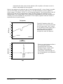
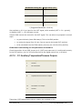
Below is an example of a spectrum pair (2f and corresponding DC = Laser Power) recorded
with the PCI-FPGA-1A controller board using a 0-5V data acquisition system scaled to a
counts range of -32768 to +32767 (i.e. 16 bit signed integers). The vertical offset in the DC
spectrum is fixed and is implemented to obtain a slightly higher bit resolution on the
digitized data. The vertical offset in the 2f spectrum is adjustable via the GUI interface and
normally set to accommodate the asymmetric 2f line shape (negative lobes are smaller in
amplitude than the positive peak.
DC Spectrum
8000
Typical DC spectrum after A/D
conversion. The null pulse provides
the DC signal chain "zero" output
in the absence of laser light, and is
especially useful for situations
where ambient stray light or
sunlight can reach the detector.
6000
ADC Counts
4000
2000
0
-2000
Null Pulse
-4000
Wavelength >>
0
64
128
192
256
320
384
448
512
Index
2f Spectrum
-4000
There is a small temporal offset in
the 2f spectrum due to
processing within the FPGA.
Separate trigger outputs allow
this offset to be measured
continuously. Phase and gain of
the 2f demodulator are adjustable
via the GUI.
-6000
ADC Counts
-8000
-10000
-12000
-14000
-16000
-18000
0
64
128
192
256
320
384
448
512
Index
PCI-FPGA-1A
4
Port City Instruments, LLC
2
Software Installation
2.1
Software files
Configuration of the PCI-FPGA-1A board is handled through a simple graphical interface that
can be downloaded from our website at: http://www.portcityinstruments.com/downloads.
Follow the instructions below to install the software on a compatible PC (running Windows™
XP (service pack 3), Vista, or Windows 7).
2.1.1
Software installation
To install the software, complete the following steps:
1. Download the Rev C flash programming software file from the following link:
http://www.portcityinstruments.com/downloads
(locate the "Rev C Programming Interface" link on the above web page). A ZIP file
contains the installer and associated programs for the flash programming graphical
interface. The file name is PCI_FPGA_RevC_Install.zip.
2. Unzip the file PCI_FPGA_RevC_Install.zip to extract the GUI application files. We
suggest making a new folder on your hard drive (e.g. C:/PCI_FPGA) and copying the
ZIP fle to this new folder prior to extraction so that the files are in a known location.
3. Double-click the file PCI_FPGA_RevC_setup.exe to install the application.
•
You may be asked to allow Windows to continue with installation without a
verifiable certificate. Click OK to allow the installation to proceed.
•
A new program will be added to the program list, which can be accessed via the
Start button (Start > All Programs > Port City Instruments, LLC > PCI-FPGA-1A
Controller).
4. Right click the new program and select Send To, then select Desktop (create
shortcut) to place the program icon on your desktop for easy future access.
NOTE: on some older XP systems we have reports that the install process
ends with an error message and asks for permission to send a report to
Microsoft. However, the application does install and run correctly despite this
message. If you see this message, simply ignore it. Check to see if the
application appears in the Start > All Programs menu. Contact us if you have
a problem with the installation.
5. Apply +5VDC power to the PCI-FPGA-1A board via the green screw terminal
connector on the side of the board (see section 3.2 for the location, and make sure
to connect the ground (GND) and +5V wires properly … do not make a connection to
the +12V terminal at this point). If the board is installed on a PC104 stack, it can
receive power via the stackthrough connector in which case make no connections to
the screw terminal connector on the board.
6. Connect the USB cable that was supplied with the board to the PCI-FPGA-1A board's
mini-USB connector.
Windows should automatically recognize that new hardware has been detected and
install the USB driver. Double click the program icon to begin programming.
Port City Instruments, LLC
5
PCI-FPGA-1A
At this point, all software is installed. The next step is to configure the FPGA's onboard
flash.
DO NOT YET CONNECT A LASER TO THE BOARD!!
It is critical to confirm that the flash is configured properly for the type
of laser being used or irreversible damage to the laser can result. We
have provided a "dummy" laser that can be used to confirm proper
laser scan parameters before connection of a real laser, and strongly
recommend that the following steps be carried out before laser
connection.
PCI-FPGA-1A
6
Port City Instruments, LLC
3
FPGA Flash Configuration
3.1
Warning
DO NOT CONNECT A LASER TO THE BOARD UNTIL YOU HAVE
FINISHED CONFIGURING THE FPGA FLASH!
It is critical to confirm that the flash is configured properly for the type of laser being used
or irreversible damage to the laser can result. We have provided a "dummy" laser that can
be used to confirm proper laser scan parameters before connection of a real laser, and
strongly recommend that the following steps be carried out before laser connection.
3.2
Configuration instructions
To configure the FPGA flash, complete the following steps:
1. Power up the PCI-FPGA-1A board. +5VDC power can be supplied to either the
auxiliary +5V input or via the PC104 bus, but not both.
See below for the location of the auxiliary power input connector (polarity is
indicated on the board silkscreen label).
NOTE: The USB port cannot supply enough +5V power to run a laser or other
circuit boards.
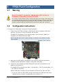
Power Connector
2. Make sure the USB cable is connected to the computer and that the software
installation steps described in Chapter 2 have been completed.
3. Launch the user interface by double-clicking the icon that you created on your
desktop in the Section 2.
Or navigate to the program from Start > All Programs > Port City Instruments, LLC
> PCI-FPGA-1A Controller.
Select a USB device number from the dropdown list at the top, left of the GUI.
•
If you only have one PCI-FPGA-1A board connected via a USB port then there
should be only one entry in the dropdown list (number "1").
Port City Instruments, LLC
7
PCI-FPGA-1A
•
If there are multiple entries make sure to select the device number
corresponding to the board being programmed. If in doubt, connect only one
board to the PC at a time (recommended).
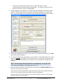
4. Initial parameters are read from the FPGA flash and displayed in the Flash Control
window. (Default parameters are programmed before shipping for a typical DFB
laser.). A screen capture of the GUI with typical DFB laser settings is shown below.
5. Change any parameter by typing a new value into the text box and clicking the Set
button within each category.
6. For the demodulator gain and phase, use the sliders. These update when the mouse
button is released (for example, slide the blue dot to a new value using the mouse
with the left button held down, then release the mouse button to activate the new
setting).
NOTE: Changes to the laser scan waveform (parameters C1, C2 and C3) take
about 3-4s to update as 2048 values have to be transferred to the flash. All
other parameters update in (typically) well under 1s.
7. Once all values have been set correctly from the GUI, click Save to Flash button to
write the new values to the flash.
These values will be automatically restored at each power up and USB connection
to a PC is not required unless you need to modify a parameter.
Read through the following description of each parameter so that you can set the
board up properly for your laser.
PCI-FPGA-1A
8
Port City Instruments, LLC
Field
Description
Frequency (Hz)
1f modulation frequency.
This should generally be in the range 31,200 Hz to 31,600 Hz for
compatibility with internal filters.
Leave this at the factory default near 31.4 KHz unless there is
good reason to deviate from that value (e.g. if you have other
instrumentation that coincidently uses this same frequency).
1f Level (%)
Peak-to-peak amplitude of the (sinusoidal) 1f modulation on the
laser current.
It is entered as a percentage of the maximum modulation
amplitude possible, which is 1/4 of the maximum laser current (or
50 mA).
Contact us if you need to change this current limit (e.g. for VCSEL
lasers or other lower current lasers) after the board has been
received.
Bandwidth (Hz)
Controls the bandwidth of software filters within the FPGA.
The input detector signal is passed through a preamplifier
configured for either an InGaAs detector or an InAs detector. An
A/D converter digitizes the signal after the preamp where it is
passed to the FPGA for processing.
This setting should generally be left at the factory default near
1219 Hz.
This setting also (partially) controls the temporal delay between
the 2f spectral line and the corresponding direct transmission
spectrum. (This delay is caused by the internal FPGA signal
processing time.) Values too high or too low can cause "ringing" in
the 2f spectrum, so experiment with this value carefully before
changing it from the factory default.
See the discussion for connector J10 for additional information on
the 2f vs. DC spectrum temporal delay as a function of the
bandwidth setting.
Ramp Period (ms)
Sets the base laser scan period in ms.
The software adjusts this number to the closest hard setting that
is available from the FPGA (eg. entering 200 ms for a 5 Hz laser
sweep rate may produce a value of 196 ms).
Valid values are from 10,000 ms (0.1 Hz rate) to 100 ms (10 Hz
sweep rate). Contact us for faster scan rates (up to 50 Hz).
Table continued on next page
Port City Instruments, LLC
9
PCI-FPGA-1A
Field
Description
2F Output Bias (%)
Controls the voltage offset of the 2f spectrum and should
generally be close to 60%.
The output 2f spectrum from the FPGA cannot be zero based with
a single 5V power supply system because the signal swings both
positively and negatively relative to the baseline. The actual
voltage offset is equal to 0.025 times the percentage offset
entered here.
For example, a value of 60% produces a (positive) voltage offset
of 60 * 0.025 = +1.5V. A value of 100% produces a voltage offset
of +2.5V, which is centered within the 0-5V range of the system.
Phase (degrees)
Demodulator phase.
Move the GUI slider to change the demodulator phase from 0 to
360 degrees. The correct setting for the demodulator phase, as
with any lock-in-amplifier, is best determined experimentally by
optimizing the polarity and amplitude of the 2f signal using an
oscilloscope or real-time data acquisition with display.
This setting is activated when the mouse button is released.
Table continued on next page
PCI-FPGA-1A
10
Port City Instruments, LLC
Field
Description
Gain
Demodulator gain.
Use this slider to adjust the amplitude of the 2f signal.
As with the demodulator phase, this parameter is best defined
using a real-time spectrum display. This setting is activated upon
release of mouse button.
NOTE: Always ensure that the gain is low enough
to keep the 2f signal on scale for the highest gas
concentration that is expected.
Ramp Coefficients (%)
The laser scan waveform is defined by a quadratic whose
coefficients are entered into C1, C2 and C3.
These are the:
•
constant (C1)
•
linear (C2)
•
quadratic (C3)
terms of the polynomial and are entered as a percentage of the
maximum laser current (200 mA unless ordered with an alternate
upper limit).
Only use the quadratic term if the laser tuning characteristics
have been determined (eg. using an etalon) and this parameter is
known.
In the normal case of a linear ramp, C1 is the laser scan starting
current. C2 represents the range of the scan ramp.
For example, if C1 = 25% and C2 = 25%, the laser scan would
run from 50 ma (0.25 * 200 mA) to 100 mA (50 mA starting
current, plus 0.25 * 200 = 50 mA ramp range). Values of C1 =
30% and C2 = 15% would produce a linear scan starting at 60
mA and ending at 90 mA (i.e. a 0.15 * 200 mA = 30 mA range),
and so on. See Appendix B for an example.
The Null pulse entry defines the width (in points) of a short period
at the start of each sweep where the laser current is set to zero.
The total laser scan ramp consists of 2048 points, and this value
should generally be in the range 60-90 so that the interval is long
enough to produce a flat bottom through the "DC" signal chain.
Click Update Laser Scan Waveform to rewrite the new scan
waveform to the onboard flash.
Note the Message Window messages and wait for the process to
complete before continuing (approximately 10s to write, another
10s to verify).
Save to File
Saves the waveform defined by C1, C2 and C3 to a disk file.
There are three columns ordered as array element number
(beginning at 1), raw DAC counts, and fraction of the full scale
current. For example:
1 13107 0.20000
2 13113 0.20009
3 13118 0.20017
may be the first three lines of a typical output file (with no null
pulse).
Table continued on next page
Port City Instruments, LLC
11
PCI-FPGA-1A
Field
Description
Message Window
Read-only display area showing various messages.
In particular, this area shows when a new laser scan waveform
has been successfully downloaded and verified. Watch this area
each time you change the C1, C2, and C3 parameters and
download a new scan waveform. Wait for confirmation before
entering any new parameters for the flash.
Save Parameters to Flash
Preserves all of the configured settings and saves them to the
flash drive. Be sure to execute this step each time parameters are
changed if you want the system to power up in a known state
each time.
Restore Factory Defaults
Resets the values in all fields to the default settings that existed
when the software was originally shipped.
Reset Board
Hard reset of all board control parameters. Warning … use this
only if data in the flash has been corrupted and all other steps to
correct the problem have failed. Requires reentry of each
parameter (or follow by clicking the Restore All Default
Parameters button to reset with default values).
PCI-FPGA-1A
12
Port City Instruments, LLC
4
Hardware Description
4.1
Hardware overview
The default configuration of the PCI-FPGA-1A board (as shipped) is for a standard
distributed feedback (DFB) tunable diode laser (TDL) and an InGaAs detector. Some
modifications may be necessary before operating lasers with higher current requirements
(for example, ICL or QC lasers) or for the use of InAs or HgCdTe detectors. Please take a
moment to examine the diagrams in Appendix A, which detail the function of each input and
output pin on the circuit board, as well as the various jumper settings and their locations.
4.2
PCI-FPGA-1A board headers
All board connectors except for J17 are standard 0.10" pin spacing (J17 is 2mm pin
spacing). Both latching and non-latching mating connectors can be used for connections to
the board and are available from most of the electronics part suppliers as Molex part
numbers (Digikey, Mouser, Jameco, Allied, Newark, etc.). For example, the mating
connector for the 2-pin laser drive is Digikey part number WM2900-ND, and for the 3-pin
detector connectors the Digikey part number is WM2901-ND.
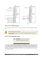
The gain of the input preamp is set by the only potentiometer on the board shown in the
photo above near the detector input connectors. This potentiometer should be adjusted to
maintain an on-scale signal <5.0V) at the output of the DC signal chain at the end of the
laser scan once the laser is aligned to the detector.
Port City Instruments, LLC
13
PCI-FPGA-1A
If the laser power spectrum begins to flatten out at the right side of the DC signal channel
output as viewed on an oscilloscope, reduce the preamplifier gain to bring the signal back
on scale with some additional margin. See the description of JMP1 in section 4.2.3 for more
details on InGaAs and InAs detector connections.
4.2.1
Connector Pinouts
See Appendix A for a complete pinout diagram for the circuit board. The sections below
provide additional details for the various connectors and jumpers.
NOTE: All pin 1 positions (headers and jumpers) are identified on the circuit
board with square solder pads on the reverse side of the board.
J1 and J3 are industry standard PC104 headers, and are provided on the board for
compatibility with multiple board "stacks." The only pins used by the board are optional
ground, +5V and +12V power (pins B1, B3 and B9 on the PC104 bus). Many websites
contain pinout details for the PC104 bus, such as the one found at:
http://pinouts.ru/Slots/Pc104_pinout.shtml
4.2.1.1 J3: Auxiliary +5V/+12 power inputs
Pin
Description
1
Power Ground
2
+5 VDC Auxiliary Power Input
3
+12VDV Auxillary Power Input
Power can also be supplied through the PC104 bus headers, in which case J3 should be left
unconnected. Do not power the board through both J3 and the PC104 bus!
4.2.1.2 J4: Laser Drive
Pin
Description
1
Laser Cathode (-)
2
Laser Anode (+)
Laser drive connections.
NOTE: Check the silkscreen labels on the circuit board and ensure that the
laser is connected properly (cathode to (-) pin, anode to (+) pin) before
power up. Irreversible damage to the laser can result if the laser is connected
backwards. Also make sure that the programmed laser current is within the
capabilities of the laser being used. Currents exceeding the laser's specification
can damage or destroy the laser.
PCI-FPGA-1A
14
Port City Instruments, LLC
4.2.1.3 J5: InGaAs Detector Input
Pin
Description
1
Ground (shield connection)
2
Detector Cathode (-)
3
Detector Anode (+)
Connect an InGaAs detector to J5 as shown on the board silkscreen (cathode to (-) pin,
anode to (+) pin).
If you are using a shielded twisted pair or other cabling with a separate shield, also connect
the shield to the pin labeled "S" on the board silkscreen.
For InGaAs detectors, the bias jumper (JMP1) should be set to "2.5". The InAs jumper
(JMP2) should be OFF.
NOTE: It is possible to connect an InGaAs detector with zero bias (JMP1 in "0"
position), but in this case the detector connections must be reversed at J5 and
the DC spectrum polarity will be the opposite of the 2.5V reverse bias case.
4.2.1.4 J6: InAs Detector Input
Pin
Description
1
Ground (shield connection)
2
Detector Cathode (-)
3
Detector Anode (+)
Connect an InAs detector to J6 as shown on the board silkscreen (cathode to (-) pin, anode
to (+) pin).
If you are using a shielded twisted pair or other cabling with a separate shield, also connect
the shield to the pin labeled "S" on the board silkscreen.
For InAs detectors the bias jumper (JMP1) should be set to "0".
Port City Instruments, LLC
15
PCI-FPGA-1A
4.2.1.5 J7: Temperature, Amplified Pressure Sensor Inputs
Pin
Description
1
Thermistor #1 (+)
2
Thermistor #1 (Ground)
3
Thermistor #2 (+)
4
Thermistor #2 (Ground)
5
Thermistor #3 (+)
6
Thermistor #3 (Ground)
7
Amplified Pressure Sensor Output
8
Pressure Sensor Output Return (Ground)
9
+5.00V Reference for Amplified Pressure Sensor
10
Ground
Connector J7 allows connection of up to three thermistors and one amplified pressure
sensor as shown above and in Appendix A. Most amplified pressure sensors provide
ratiometric outputs that vary with the power supply.
Pin 9 of J7 provides a stable 5.00V reference voltage that can be used to power the
pressure sensor, with the ground and output signals from the pressure sensor on pins 8 and
7, respectively.
The pressure sensor output value is provided on pin 6 of J11. Typical output ranges for this
type of sensor are 0.25 to 4.75V, or 0.5 to 4.5V, but any sensor with an output in the 05VDC range can be used with the board, even if the power is provided externally (in which
case leave pin 9 unconnected).
The thermistor transfer function is Rt = (22.49 * Vin - 7.0) / (2.8112 - Vin) where Vin is the
output voltage on pins 10, 12 or 14 of J11 and Rt is the thermistor resistance in Kohm.
Conversion to temperature requires knowledge of the thermistor R vs T curve, available
from the manufacturer.
4.2.1.6 J8: Unamplified Pressure Sensor Input
Pin
Description
1
+10V Power (supplied by board)
2
Pressure Sensor (+) Output
3
Pressure Sensor (-) Output
4
Common
There are many 0-100 mV pressure sensors on the market that have a common mode
voltage between the input power and the output signal connections. The PCI-FPGA-1A board
provides a 10.0V power signal on pin 1 of J8. An on-board instrumentation amplifier circuit
effectively eliminates the common mode voltage to produce an amplified output from the
pressure on pin 4 of J11.
Nominal output range is 0 - 3.5V corresponding to the full range of the pressure sensor
(e.g. 0 - 15 PSI, 0 - 1 Bar, etc.).
PCI-FPGA-1A
16
Port City Instruments, LLC
4.2.1.7 J9: PRTD Input
Pin
Description
1
PRTD Bias
2
PRTD (+)
3
PRTD (-)
4
Ground
J9 provides a small bias current for use with 1000 ohm PRTD platinum resistance
temperature sensors. The output voltage from the sensor is provided on pin 8 of J11 with a
transfer function of Rprt = 495.52 * Vin, where Vin is the voltage on J11 pin 8, and Rprt is
the Pt sensor resistance.
Conversion to temperature can then be made using the manufacturer's data for the PRTD
sensor element.
4.2.1.8 J10: Auxiliary Outputs
Pin
Description
1
Ground
2
Trigger #1 (synched with DC spectrum)
3
Ground
4
Trigger #2 (synched with 2f spectrum)
5
Ground
6
External Laser Off (LOFF)
7
Ground
8
2f Spectrum Output
9
Ground
10
DC Spectrum (laser power) Output
J10 provides the trigger and spectrum outputs from the DC and 2f signal chains.
There are two trigger outputs (3.3V amplitude, approximately 110 us in width).
•
Trigger 1 is synchronized with the DC spectrum scan start.
•
Trigger 2 is synchronized with the 2f spectrum.
The delay between these two trigger outputs is equal to the temporal delay between the DC
and 2f spectra and can be used by the acquisition software to properly normalize the 2f
spectrum to laser power. Approximate values for the delay between Trigger 1 and Trigger 2
as a function of the bandwidth setting are:
Port City Instruments, LLC
17
PCI-FPGA-1A
Bandwidth Setting (Hz)
Trigger Delay (ms)
250
82.0
500
41.5
750
27.0
1000
21.0
1250 (1219)*
16.4 (16.8)
1500
15.4
1750
13.4
2000
10.3
* (Suggested Bandwidth: 1219 Hz)
Also resident on J10 is an input for the LOFF signal, which enables (LOFF = 0V = ground),
or disables (LOFF = +5V) the laser current.
Jumper JMP6 controls the source for the LOFF signal. This can either be jumpered in several
ways:
•
to ground directly (laser ON always). This is the GND position.
•
to receive the signal from J10 pin 6 as an input to the board (EXT position)
•
to be controlled from the FPGA (factory use only, do not shunt this position)
If the laser is not turning on and you believe it should be
Check the position of the JMP6 jumper pin 6 (LOFF) and make sure it is configured correctly.
In the EXT position, pin 6 of J10 must be wired to a a digital control line, or a switch.
4.2.1.9 J11: Auxiliary Temperature/Pressure Outputs
Pin
Description
1
Ground
2
No connection
3
Ground
4
Unamplified Pressure Sensor Output
5
Ground
6
Amplified Pressure Sensor Output
7
Ground
8
PRTD Output
9
Ground
10
Thermistor #1 Output
11
Ground
12
Thermistor #2 Output
13
Ground
14
Thermistor #3 Output
Thermistor, PRTD and pressure sensor outputs are provided on J11.
PCI-FPGA-1A
18
Port City Instruments, LLC
Transfer functions have been described earlier in the descriptions of the input connectors.
They are also repeated in sections 4.2.4 (Thermistor conversions), and section 4.2.5
(Pressure sensor conversions (absolute P sensors).
Port City Instruments, LLC
19
PCI-FPGA-1A
4.2.2
Other Connector Pinouts
Connectors J12-J15 and J20-J22 are used only when the PCI-FPGA-1A board is interfaced to
the Diamond System Helios™ CPU board (with DAQ subsystem) having spare digital and
analog input and output channels. These are provided for miscellaneous functions such as
LED control, trigger signals, or other general use functions not related to operation of the
PCI-FPGA-1A board itself. They pass through connector J17 and only have utility if
connected to an external I/O system through J17 (and wired according to the Helios CPU
board's DAQ connector).
4.2.2.1 J12: Utility Analog Output (Helios Vout0)
Pin
Description
1
Utility Analog Output
2
Ground
4.2.2.2 J13: Utility Analog Output (Helios Vout1)
Pin
Description
1
Utility Analog Output
2
Ground
4.2.2.3 J14: Utility Analog Output (Helios Vout2)
Pin
Description
1
Utility Analog Output
2
Ground
4.2.2.4 J15: Utility Analog Output (Helios Vout3)
PCI-FPGA-1A
Pin
Description
1
Utility Analog Output
2
Ground
20
Port City Instruments, LLC
4.2.2.5 J20: Utility Analog Input (Helios Vin10)
Pin
Description
1
Utility Analog Input
2
Ground
4.2.2.6 J21: Utility Digital Input (Helios DIO A2)
Pin
Description
1
Utility Digital Input
2
Ground
4.2.2.7 J22: Utility Digital Output (Helios DIO B2)
Pin
Description
1
Utility Digital Output
2
Ground
4.2.2.8 J16: Mini USB Connector for FPGA Setup
Pin
Description
1
Bus Voltage
2
D-
3
D+
4
ID
5
Ground
J16 is a mini-USB connector that is used for updating the laser control and demodulator
parameters via the interface GUI. A mating cable is provided with the board, or any
standard mini-USB cable can be used.
4.2.2.9 J17: 50-Pin I/O Header (alternate external I/O system interface)
J17 is used for direct interface to the Diamond Systems Helios™ CPU board (or any other
external I/O system). The relevant pin connections are shown in the diagram on the next
page simply to indicate how this interface is configured. This CPU board has onboard 16-bit
I/O and can be used to build a complete 2f gas sensor with only a single +5VDC power
supply and 2-board PC104 stack.
Please contact us for more information on operating the PCI-FPGA-1A board using the
Helios™ CPU board.
Port City Instruments, LLC
21
PCI-FPGA-1A
4.2.2.10 J18: JTAG Connector
Do not make connections to J18. It is not user accessible. It is used to program the FPGA
core.
Do not make connections to J18.
Any voltage applied to these pins can potentially damage the FPGA chip or corrupt the
internal program.
4.2.2.11 J2: Diagnostics Header
Pin
Description
1
Trigger #1 (synched to DC spectrum)
2
2f Spectrum
3
DC (laser power) Spectrum
The Trigger1, 2f and DC spectrum signals on J2 are duplicates of the corresponding signals
on J10, but with isolation resistors provided (4.75K for Trigger #1 and the 2f signal, 1K for
the DC signal). These are useful for monitoring the signals with a high impedance device
such as an oscilloscope during setup, laser alignment, etc. The signals on J10 are best used
for direct connection to an external A/D converter, or when Trigger #2 (synchronous with
the 2f signal) is needed.
PCI-FPGA-1A
22
Port City Instruments, LLC
4.2.2.12 J19: External Preamp Voltage Input
Pin
Description
1
V- (ground)
2
V+ (preamp output, 0-10V range only)
J19 is used only for a factory option that must be specified at order. It allows the board to
accept the voltage output from an external preamplifier rather than receiving a detector
input directly. Please contact us, or your distributor to order boards configured for this
option. For direct detector input, make no connections to J19.
4.2.3
Jumper configuration
Please refer to the diagrams in Appendix A for the location of the jumper blocks described
below. These drawings are also available as PDF files on the USB flash drive supplied with
the board.
Default Jumper Positions
Jumper
Function
Default Position
JMP1
Detector Bias
Shunt on pins 2-3 (2.5V reverse bias)
JMP2
InAs Detector Select
No shunt (pins open)
JMP3
2f signal pin connection to J17
Vin1 (DC)
JMP4
DC signal pin connection to J17
Vin0 (2f)
JMP5
2f channel output time constant
select
4.1 ms
JMP6
LOFF digital laser ON/OFF control
line
EXT
JMP7
USB power ON/OFF select
ON (USB +5V connected to board
power)
JMP8
Laser drive power select
Shunt on pins 1-2 (+5V)
JMP9
Preamp voltage input select
No shunt (no connection to J19)
JMP1: Detector reverse bias jumper (shunt on pins 1-2 = 0V bias, shunt on pins 2-3 =
2.5V reverse bias). InGaAs detectors should be operated with the shunt in positions 2-3
(2.5V reverse bias) and with jumper JMP2 removed (open). InAs detectors should be
operated with the shunt in positions 1-2 (0V bias), and with a shunt on jumper JPM2.
The default position is 2-3 for InGaAs detectors, 2.5V reversed biased.
NOTE: Photovoltaic HgCdTe detectors such as those sold by Vigo can generally be
connected to the InAs input for use with mid-IR lasers such as interband cascade
or quantum cascade lasers. Jumper for InAs detector input.
It is also possible to use an InGaAs detector with zero bias (JMP1 shut in positions 1-2, or
"0 on the silkscreen"). In this case:
•
JMP2 must be open (as always for InGaAs detectors)
•
The InGaAs detector must be connected backwards relative to the silkscreen
labels (ie. the detector cathode should be connected to the (+) pin and the
detector anode to the (-) pin).
Port City Instruments, LLC
23
PCI-FPGA-1A
The DC spectrum with this connection scheme will be reversed in polarity relative to the
normal reversed biased connection, as will the 2f spectrum (the demodulator phase for the
2f signal should be changed by 180 degrees on the GUI). It is recommended to always run
an InGaAs detector with reverse bias if possible (JMP1 shunt in positions 2-3, JPM2 open,
detector connections as per the board silkscreen).
JMP2: InAs detector jumper selector (ON = InAs connected, OFF = InGaAs connected). See
comments for JMP1. This jumper should only be closed if an InAs detector is connected to
J6, and JMP1 is shunted for zero bias.
The default position is OFF for InGaAs detectors.
JMP3: 2f output signal pin designation. This jumper is used, along with JMP4, to configure
the connections at J17 for interfacing two PCI-FPGA-1A boards to the Diamond System's
Helios™ CPU board. It should normally be left in Vin1 position (see description for J17, and
Appendix A diagram). Together with JMP4, the 2f and DC outputs from the board can be
transferred to alternate A/D input pins at J17.
The default position is Vin1 = J17 pin 2F-1.
JMP4: DC output signal pin designation. See comments for JMP3 (this jumper serves the
same function but for the DC spectrum output).
The default position is Vin0 = J17 pin DC-1.
JMP5: 2f channel output time constant selector (0.6, 1.3, 1.9 and 4.1 ms). Apply a shunt to
one of the five available time constant selections to set the low pass filter time constant for
the demodulator output section. There is an open position for installation of a user-defined
capacitor if a time constant >4.1 ms is required. The relationship is:
C(Farad) = τ / ([2 * pi * 2000)
where τ is the desired time constant in seconds, and pi = 3.141592.
The default position is 0.6 ms (minimum value).
JMP6: LOFF (laser enable) source selector (on-board, external or FPGA). JMP6 provides
options for controlling a digital line ("LOFF") that is used to enable, or disable, current to the
laser. When LOFF is +5V the laser current is disabled, and when LOFF is tied to power
ground, laser current is enabled. LOFF is pulled up to +5V via a 20K pullup resistor on the
board. The three available jumper positions as indicated on the board silkscreen and in
Appendix A (use PDF files for the Appendix A drawing supplied on the install USB drive for
clearer views) are:
•
GND – the LOFF is hard grounded which enables laser current at all times. Be
very careful with this setting as the LOFF function is effectively disabled.
•
EXT – the LOFF signal is provided externally either via J10 or J17 (if interfaced to
the Diamond Systems Helios™ CPU board).
•
FPGA - the LOFF pin is controlled by the FPGA itself (factory use only … do not
use this jumper option).
In general, JMP6 should be in the:
•
EXT position if the board is being controlled via an external I/O system with an
available digital line, or if a mechanical switch is used for laser ON/OFF.
•
GND position for testing using a dummy resistor in place of the laser. Can also be
used if it is certain no power-on transients at up to 200 mA will cause damage.
The default position is EXT.
PCI-FPGA-1A
24
Port City Instruments, LLC
JMP7: USB power selector. A shunt on these pins allows the UART interfaced to the flash
chip to be powered by the same +5V source powering the board (PC104 bus, or the
auxiliary power input). With this shunt removed the UART is powered by the USB cable (i.e.
the PC the USB cable is connected to).
If programming a bare board (i.e. not on a powered PC104 stack, and no auxiliary power
input) leave JMP7 open (no shunt).
If programming a board connected to auxiliary power or powered through the PC104 bus,
apply the shunt to JMP7.
JMP8: Laser drive power source. Unless the circuit board is ordered for ICL or QC laser
compliance capability, leave this jumper set for +5V laser drive power (default). With other
component changes it is possible to use a +12V source (input via the auxillary power screw
terminal connector) to produce up to 10.7V compliance for QC lasers. Contact us for circuit
boards configured for ICL or QC lasers.
The default position is +5V.
JMP9: Preamp input voltage select. This is a factory option only. The circuit board can be
configured to accept the voltage from an external preamp rather than a detector input. This
requires component changes on the circuit board and the shunt should be left in the "InAs"
position for normal board operation. This position does not select InAs detector input as
long as JMP2 is open … JMP9 is used in conjunction with JMP2 for voltage input).
The default position is InAs.
4.2.4
Thermistor conversions
Rt = (22.49 * Vin - 7.0) / (2.8112 - Vin), where Rt is the thermistor resistance in Kohm and
Vin is the output voltage provided by the PCI-FPGA-1A board. The useful range of
thermistor resistances is between approximately 0.125 Kohm (Vin = 0.325V) to 488 Kohm
(Vin = 2.701V). Outside of these ranges the change in Vin with respect to Rt is extremely
large.
For a typical 10 Kohm @ 25C thermistor with a beta value near 3900, this represents a
temperature range of roughly -45C to +165C, with larger errors at the extremes of the
range (especially the high temperature end where Rt is very small). Make sure to use a
thermistor with a resistance value within the above range for valid output values, and
match it to the best performance over the full temperature range of the application.
4.2.5
Pressure sensor conversions (absolute P sensors)
•
Amplified sensor: No conversion. The board outputs the sensor voltage from the
absolute pressure sensor with no amplification or scaling.
•
Unamplified 0 - 100 mV sensors: Linear output, 0 to Pmax = 0 to Vmax, where
Vmax is 3.5V (nominal) and Pmax is the upper limit of the pressure sensor. Each
pressure sensor should be calibrated with the board for precise determination of
Vmax and any DC offset that may be present.
Port City Instruments, LLC
25
PCI-FPGA-1A
4.2.6
PRTD conversion
Rprt = 495.52 * Vin, where Rprt is the resistance of the PRTD and Vin is the voltage output
from the PCI-FPGA-1A board.
Conversion of Rprt to temperature can be done using the appropriate calibration curve for
the PRTD being used.
PCI-FPGA-1A
26
Port City Instruments, LLC
5
Troubleshooting
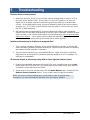
No laser drive current present
1. Make sure the LOFF shunt is in the correct position as described in section 4.2.3 of
this user guide, jumper JMP6. If this shunt is in the "EXT" position, an external
digital line or a switch must be configured to ground the LOFF pin to enable laser
current. In the GND position laser current is allowed to pass at all times (including
at power up). The "FPGA" position should never be used (ie. shunt must only be on
the EXT or GND positions).
2. GUI has not been programmed for a current range that is above laser threshold.
Double check the currents programmed in the GUI, and if necessary replace the laser
with a 10 ohm, 1/2W resistor and measure the current directly (do not ground either
side of this resistor … use a scope probe on each side separately and measure the
difference, with the scope probe ground lead tied to power ground).
Interface shows zeros in all places at program start
1. This is usually caused by selection of the wrong USB device number, or a bad USB
cable connection between the board and the PC. Double check the cable connections,
and restart the GUI program if necessary.
2. This can also be caused by an overloaded USB port. Make sure there is sufficient
USB power for an extra device (Windows generally displays an errror message if a
USB port is overloaded).
2f channel output is extremely noisy with no laser light on detector (rare)
1. Change the bandwidth parameter on the GUI (by even one digit) and click the Set
button below the entry text box. This resets the internal filters if they have become
corrupted in some way within the FPGA.
2. If this doesn't solve the problem then click the Reset Board button, followed by the
Restore Factory Defaults button. This is a laser resort to clear the problem
NOTE: Be sure to note all settings prior to this step in order to reenter them
manually if you have used values that differ from the factory defaults.
Port City Instruments, LLC
27
PCI-FPGA-1A
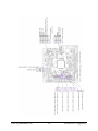
Appendix A: Board Pinouts (Rev C)
Port City Instruments, LLC
29
PCI-FPGA-1A
Port City Instruments, LLC
30
PCI-FPGA-1A - Appendices
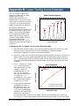
Appendix B: Laser Tuning Curve Example
The spacing between the
transmission peaks is equal to the
free spectral range (FSR) of the
etalon, which can be calculated
from the physical length of the
etalon and the known index of
refraction of the etalon material
at the temperature and
wavelength of interest*. In this
example the free spectral range is
0.228 cm-1.
Etalon Transmission Spectrum
65.78008
FSR = 0.2280 cm-1
3000
Transmission
The C1, C2 and C3 laser scan
waveform coefficients are best
determined using the
transmission spectrum of a
suitable etalon. The figure to the
right is such a spectrum recorded
using a 15 mm long fused silica
etalon and a 1530 nm DFB laser.
60.93151
55.79452
50.24658
44.15068
2000
37.0274
1000
0
30
35
40
45
50
55
60
65
Laser Current (mA)
To determine C1, C2 and C3, carry out the following steps
1. Scan the laser current linearly over a chosen range by setting C3 equal to 0.0 and
defining a linear ramp with the C1 and C2 parameters. Record the etalon
transmission spectrum as shown in the example above.
2. Locate the centers of the etalon transmission peaks to define the laser current at the
peak centers. Since the spacing between the etalon transmission peaks is fixed (in
cm-1)*, and the laser tuning is nonlinear with current (laser tunes faster as current
increases), the spacing between the etalon peaks (in mA) will vary across the scan
as shown.
Laser Tuning Curve
70
Data
Quadratic Fit
65
60
Laser Current (mA)
3. Plot x = relative cm-1 value
vs. y = laser current at
each etalon peak. For this
example, peak #1
coordinates are x = 0.0
cm-1, y = 37.0274 mA,
peak #2 coordinates are x
= 0.2280 cm-1, y =
44.15068 mA, , etc. where
the x coordinate of peak n
is equal to (n-1)*FSR.
55
50
45
4. Fit the resulting data with
40
Y =37.1555+30.97526 X-5.22454 X2
a quadratic as shown in
C1 = 18.58, C2 = 15.49, C3 = -2.61
35
the plot to the right. The
fit coefficients are in mA.
0.0
0.2
0.4
0.6
0.8
1.0
1.2
To convert to percentages
Relative Wavenumber
needed by the control GUI,
divide each coefficient by
the maximum laser current for the board (200 mA is the default) and multiply by
100 to get %. These coefficients can then be entered into the GUI to cause the laser
Port City Instruments, LLC
31
PCI-FPGA-1A
to scan linearly in cm-1 via an appropriate nonlinear (quadratic) ramp in laser
current.
* The etalon FSR, to first order, is equal to c / (2ηL) where c is the speed of light, η is the
material index of refraction, and L is the etalon thickness (or spacing). Both η and L are
temperature dependent, and η is also wavelength dependent. Over the short tuning range
of a typical DFB laser, η can be considered constant and the etalon peak spacings are
constant in cm-1.
Port City Instruments, LLC
32
PCI-FPGA-1A - Appendices