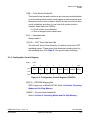
1
68HC11M6
HC11M68HC
1M68HC11M
M68HC11E/D
REV 3.2
M68HC11E Family
Technical Data
HCMOS
Microcontroller Unit
blank
MC68HC11E Family
Technical Data
Motorola reserves the right to make changes without further notice to any products
herein. Motorola makes no warranty, representation or guarantee regarding the
suitability of its products for any particular purpose, nor does Motorola assume any
liability arising out of the application or use of any product or circuit, and specifically
disclaims any and all liability, including without limitation consequential or incidental
damages. "Typical" parameters which may be provided in Motorola data sheets and/or
specifications can and do vary in different applications and actual performance may
vary over time. All operating parameters, including "Typicals" must be validated for
each customer application by customer’s technical experts. Motorola does not convey
any license under its patent rights nor the rights of others. Motorola products are not
designed, intended, or authorized for use as components in systems intended for
surgical implant into the body, or other applications intended to support or sustain life,
or for any other application in which the failure of the Motorola product could create a
situation where personal injury or death may occur. Should Buyer purchase or use
Motorola products for any such unintended or unauthorized application, Buyer shall
indemnify and hold Motorola and its officers, employees, subsidiaries, affiliates, and
distributors harmless against all claims, costs, damages, and expenses, and
reasonable attorney fees arising out of, directly or indirectly, any claim of personal
injury or death associated with such unintended or unauthorized use, even if such claim
alleges that Motorola was negligent regarding the design or manufacture of the part.
Motorola, Inc. is an Equal Opportunity/Affirmative Action Employer.
Motorola and
are registered trademarks of Motorola, Inc.
DigitalDNA is a trademark of Motorola, Inc.
0&+&()DPLO\²5HY
027252/$
© Motorola, Inc., 2001
7HFKQLFDO'DWD
7HFKQLFDO'DWD
To provide the most up-to-date information, the revision of our
documents on the World Wide Web will be the most current. Your printed
copy may be an earlier revision. To verify you have the latest information
available, refer to:
http://www.motorola.com/mcu/
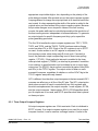
The following revision history table summarizes changes contained in
this document. For your convenience, the page number designators
have been linked to the appropriate location.
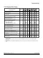
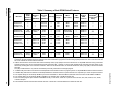
Revision History
Date
May, 2001
June, 2001
7HFKQLFDO'DWD
Revision
Level
3.1
3.2
Description
Page
Number(s)
4.4.3.1 System Configuration Register — Addition to NOCOP
bit description
88
Added 11.22 EPROM Characteristics
251
11.22 EPROM Characteristics — For clarity, addition to note 2
following the table
251
0&+&()DPLO\²5HY
027252/$
Technical Data — M68HC11E Family
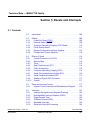
List of Sections
Section 1. General Description . . . . . . . . . . . . . . . . . . . . 23
Section 2. Pin Descriptions . . . . . . . . . . . . . . . . . . . . . . . 27
Section 3. Central Processor Unit (CPU) . . . . . . . . . . . . 45
Section 4. Operating Modes and On-Chip Memory . . . . 65
Section 5. Resets and Interrupts . . . . . . . . . . . . . . . . . . 107
Section 6. Parallel Input/Output (I/O) Ports . . . . . . . . . 133
Section 7. Serial Communications Interface (SCI) . . . . 145
Section 8. Serial Peripheral Interface (SPI). . . . . . . . . . 165
Section 9. Timing System. . . . . . . . . . . . . . . . . . . . . . . . 177
Section 10. Analog-to-Digital (A/D) Converter . . . . . . . 209
Section 11. Electrical Characteristics . . . . . . . . . . . . . . 221
Section 12. Mechanical Data . . . . . . . . . . . . . . . . . . . . . 253
Section 13. Ordering Information . . . . . . . . . . . . . . . . . 261
Appendix A. Development Support . . . . . . . . . . . . . . . . 269
Appendix B. EVBU Schematic . . . . . . . . . . . . . . . . . . . . 275
M68HC11E Family — Rev. 3.1
MOTOROLA
Technical Data
List of Sections
5
List of Sections
AN1060 — M68HC11 Bootstrap Mode . . . . . . . . . . . . . 277
EB184 — Enabling the Security Feature
on the MC68HC711E9 Devices with PCbug11
on the M68HC711E9PGMR . . . . . . . . . . . . . . . . . . . 323
EB188 — Enabling the Security Feature
on M68HC811E2 Devices with PCbug11
on the M68HC711E9PGMR . . . . . . . . . . . . . . . . . . . 327
EB296 — Programming MC68HC711E9 Devices
with PCbug11 and the M68HC11EVBU . . . . . . . . . 331
Technical Data
6
M68HC11E Family — Rev. 3.1
List of Sections
MOTOROLA
Technical Data — M68HC11E Family
Table of Contents
Section 1. General Description
1.1
Contents . . . . . . . . . . . . . . . . . . . . . . . . . . . . . . . . . . . . . . . . . . 23
1.2
Introduction . . . . . . . . . . . . . . . . . . . . . . . . . . . . . . . . . . . . . . . . 23
1.3
Features . . . . . . . . . . . . . . . . . . . . . . . . . . . . . . . . . . . . . . . . . . 24
1.4
Structure . . . . . . . . . . . . . . . . . . . . . . . . . . . . . . . . . . . . . . . . . . 25
Section 2. Pin Descriptions
2.1
Contents . . . . . . . . . . . . . . . . . . . . . . . . . . . . . . . . . . . . . . . . . . 27
2.2
Introduction . . . . . . . . . . . . . . . . . . . . . . . . . . . . . . . . . . . . . . . . 28
2.3
VDD and VSS . . . . . . . . . . . . . . . . . . . . . . . . . . . . . . . . . . . . . . . 32
2.4
RESET . . . . . . . . . . . . . . . . . . . . . . . . . . . . . . . . . . . . . . . . . . . 34
2.5
Crystal Driver and External Clock Input
(XTAL and EXTAL) . . . . . . . . . . . . . . . . . . . . . . . . . . . . . . . 35
2.6
E-Clock Output (E) . . . . . . . . . . . . . . . . . . . . . . . . . . . . . . . . . . 36
2.7
Interrupt Request (IRQ) . . . . . . . . . . . . . . . . . . . . . . . . . . . . . . 36
2.8
Non-Maskable Interrupt (XIRQ/VPPE). . . . . . . . . . . . . . . . . . . .36
2.9
MODA and MODB (MODA/LIR and MODB/VSTBY) . . . . . . . . . 37
2.10
VRL and VRH . . . . . . . . . . . . . . . . . . . . . . . . . . . . . . . . . . . . . . . 38
2.11
STRA/AS . . . . . . . . . . . . . . . . . . . . . . . . . . . . . . . . . . . . . . . . . 38
2.12
STRB/R/W . . . . . . . . . . . . . . . . . . . . . . . . . . . . . . . . . . . . . . . . 38
2.13 Port Signals . . . . . . . . . . . . . . . . . . . . . . . . . . . . . . . . . . . . . . . 39
2.13.1 Port A . . . . . . . . . . . . . . . . . . . . . . . . . . . . . . . . . . . . . . . . . . 39
2.13.2 Port B . . . . . . . . . . . . . . . . . . . . . . . . . . . . . . . . . . . . . . . . . . 41
2.13.3 Port C . . . . . . . . . . . . . . . . . . . . . . . . . . . . . . . . . . . . . . . . . . 42
2.13.4 Port D . . . . . . . . . . . . . . . . . . . . . . . . . . . . . . . . . . . . . . . . . . 43
2.13.5 Port E . . . . . . . . . . . . . . . . . . . . . . . . . . . . . . . . . . . . . . . . . . 43
M68HC11E Family — Rev. 3.2
MOTOROLA
Technical Data
Table of Contents
7
Table of Contents
Section 3. Central Processor Unit (CPU)
3.1
Contents . . . . . . . . . . . . . . . . . . . . . . . . . . . . . . . . . . . . . . . . . . 45
3.2
Introduction . . . . . . . . . . . . . . . . . . . . . . . . . . . . . . . . . . . . . . . . 46
3.3
CPU Registers . . . . . . . . . . . . . . . . . . . . . . . . . . . . . . . . . . . . . 46
3.3.1
Accumulators A, B, and D . . . . . . . . . . . . . . . . . . . . . . . . . . 47
3.3.2
Index Register X (IX) . . . . . . . . . . . . . . . . . . . . . . . . . . . . . . 48
3.3.3
Index Register Y (IY) . . . . . . . . . . . . . . . . . . . . . . . . . . . . . . 48
3.3.4
Stack Pointer (SP) . . . . . . . . . . . . . . . . . . . . . . . . . . . . . . . . 48
3.3.5
Program Counter (PC) . . . . . . . . . . . . . . . . . . . . . . . . . . . . .50
3.3.6
Condition Code Register (CCR) . . . . . . . . . . . . . . . . . . . . . . 51
3.3.6.1
Carry/Borrow (C) . . . . . . . . . . . . . . . . . . . . . . . . . . . . . . . 51
3.3.6.2
Overflow (V) . . . . . . . . . . . . . . . . . . . . . . . . . . . . . . . . . . . 51
3.3.6.3
Zero (Z) . . . . . . . . . . . . . . . . . . . . . . . . . . . . . . . . . . . . . .51
3.3.6.4
Negative (N) . . . . . . . . . . . . . . . . . . . . . . . . . . . . . . . . . . . 52
3.3.6.5
Interrupt Mask (I) . . . . . . . . . . . . . . . . . . . . . . . . . . . . . . . 52
3.3.6.6
Half Carry (H) . . . . . . . . . . . . . . . . . . . . . . . . . . . . . . . . . .52
3.3.6.7
X Interrupt Mask (X) . . . . . . . . . . . . . . . . . . . . . . . . . . . . .52
3.3.6.8
STOP Disable (S) . . . . . . . . . . . . . . . . . . . . . . . . . . . . . . 53
3.4
Data Types . . . . . . . . . . . . . . . . . . . . . . . . . . . . . . . . . . . . . . . . 53
3.5
Opcodes and Operands . . . . . . . . . . . . . . . . . . . . . . . . . . . . . . 53
3.6
Addressing Modes . . . . . . . . . . . . . . . . . . . . . . . . . . . . . . . . . . 54
3.6.1
Immediate. . . . . . . . . . . . . . . . . . . . . . . . . . . . . . . . . . . . . . . 54
3.6.2
Direct . . . . . . . . . . . . . . . . . . . . . . . . . . . . . . . . . . . . . . . . . . 55
3.6.3
Extended . . . . . . . . . . . . . . . . . . . . . . . . . . . . . . . . . . . . . . . 55
3.6.4
Indexed. . . . . . . . . . . . . . . . . . . . . . . . . . . . . . . . . . . . . . . . . 55
3.6.5
Inherent . . . . . . . . . . . . . . . . . . . . . . . . . . . . . . . . . . . . . . . . 55
3.6.6
Relative . . . . . . . . . . . . . . . . . . . . . . . . . . . . . . . . . . . . . . . . 56
3.7
Instruction Set. . . . . . . . . . . . . . . . . . . . . . . . . . . . . . . . . . . . . .56
Technical Data
8
M68HC11E Family — Rev. 3.2
Table of Contents
MOTOROLA
Table of Contents
Section 4. Operating Modes and On-Chip Memory
4.1
Contents . . . . . . . . . . . . . . . . . . . . . . . . . . . . . . . . . . . . . . . . . . 65
4.2
Introduction . . . . . . . . . . . . . . . . . . . . . . . . . . . . . . . . . . . . . . . . 66
4.3
Operating Modes . . . . . . . . . . . . . . . . . . . . . . . . . . . . . . . . . . . 66
4.3.1
Single-Chip Mode. . . . . . . . . . . . . . . . . . . . . . . . . . . . . . . . . 66
4.3.2
Expanded Mode . . . . . . . . . . . . . . . . . . . . . . . . . . . . . . . . . .67
4.3.3
Test Mode . . . . . . . . . . . . . . . . . . . . . . . . . . . . . . . . . . . . . .67
4.3.4
Bootstrap Mode . . . . . . . . . . . . . . . . . . . . . . . . . . . . . . . . . . 68
4.4
Memory Map. . . . . . . . . . . . . . . . . . . . . . . . . . . . . . . . . . . . . . . 69
4.4.1
RAM and Input/Output Mapping. . . . . . . . . . . . . . . . . . . . . . 80
4.4.2
Mode Selection. . . . . . . . . . . . . . . . . . . . . . . . . . . . . . . . . . . 82
4.4.3
System Initialization . . . . . . . . . . . . . . . . . . . . . . . . . . . . . . . 85
4.4.3.1
System Configuration Register . . . . . . . . . . . . . . . . . . . . 86
4.4.3.2
RAM and I/O Mapping Register . . . . . . . . . . . . . . . . . . . .89
4.4.3.3
System Configuration Options Register . . . . . . . . . . . . . . 91
4.5
EPROM/OTPROM . . . . . . . . . . . . . . . . . . . . . . . . . . . . . . . . . . 92
4.5.1
Programming an Individual EPROM Address . . . . . . . . . . . 93
4.5.2
Programming the EPROM with Downloaded Data. . . . . . . . 94
4.5.3
EPROM and EEPROM Programming
Control Register . . . . . . . . . . . . . . . . . . . . . . . . . . . . . . . 94
4.6
EEPROM . . . . . . . . . . . . . . . . . . . . . . . . . . . . . . . . . . . . . . . . . 98
4.6.1
EEPROM and CONFIG Programming and Erasure. . . . . . . 98
4.6.1.1
Block Protect Register . . . . . . . . . . . . . . . . . . . . . . . . . . . 99
4.6.1.2
EPROM and EEPROM Programming
Control Register . . . . . . . . . . . . . . . . . . . . . . . . . . . . 101
4.6.1.3
EEPROM Bulk Erase . . . . . . . . . . . . . . . . . . . . . . . . . . . 103
4.6.1.4
EEPROM Row Erase . . . . . . . . . . . . . . . . . . . . . . . . . . . 103
4.6.1.5
EEPROM Byte Erase . . . . . . . . . . . . . . . . . . . . . . . . . . . 104
4.6.1.6
CONFIG Register Programming . . . . . . . . . . . . . . . . . .104
4.6.2
EEPROM Security . . . . . . . . . . . . . . . . . . . . . . . . . . . . . . . 104
M68HC11E Family — Rev. 3.2
MOTOROLA
Technical Data
Table of Contents
9
Table of Contents
Section 5. Resets and Interrupts
5.1
Contents . . . . . . . . . . . . . . . . . . . . . . . . . . . . . . . . . . . . . . . . . 107
5.2
Introduction . . . . . . . . . . . . . . . . . . . . . . . . . . . . . . . . . . . . . . . 108
5.3
Resets. . . . . . . . . . . . . . . . . . . . . . . . . . . . . . . . . . . . . . . . . . . 108
5.3.1
Power-On Reset (POR) . . . . . . . . . . . . . . . . . . . . . . . . . . . 109
5.3.2
External Reset (RESET) . . . . . . . . . . . . . . . . . . . . . . . . . . 109
5.3.3
Computer Operating Properly (COP) Reset . . . . . . . . . . . . 110
5.3.4
Clock Monitor Reset . . . . . . . . . . . . . . . . . . . . . . . . . . . . . . 111
5.3.5
System Configuration Options Register . . . . . . . . . . . . . . . 112
5.3.6
Configuration Control Register . . . . . . . . . . . . . . . . . . . . . . 113
5.4
Effects of Reset . . . . . . . . . . . . . . . . . . . . . . . . . . . . . . . . . . . 114
5.4.1
Central Processor Unit (CPU) . . . . . . . . . . . . . . . . . . . . . . 115
5.4.2
Memory Map . . . . . . . . . . . . . . . . . . . . . . . . . . . . . . . . . . . 115
5.4.3
Timer . . . . . . . . . . . . . . . . . . . . . . . . . . . . . . . . . . . . . . . . . 115
5.4.4
Real-Time Interrupt (RTI) . . . . . . . . . . . . . . . . . . . . . . . . . . 116
5.4.5
Pulse Accumulator . . . . . . . . . . . . . . . . . . . . . . . . . . . . . . . 116
5.4.6
Computer Operating Properly (COP) . . . . . . . . . . . . . . . . . 116
5.4.7
Serial Communications Interface (SCI) . . . . . . . . . . . . . . . 116
5.4.8
Serial Peripheral Interface (SPI). . . . . . . . . . . . . . . . . . . . . 117
5.4.9
Analog-to-Digital (A/D) Converter. . . . . . . . . . . . . . . . . . . . 117
5.4.10 System . . . . . . . . . . . . . . . . . . . . . . . . . . . . . . . . . . . . . . . . 117
5.5
Reset and Interrupt Priority. . . . . . . . . . . . . . . . . . . . . . . . . . . 117
5.5.1
Highest Priority Interrupt and Miscellaneous Register . . . . 119
5.6
Interrupts. . . . . . . . . . . . . . . . . . . . . . . . . . . . . . . . . . . . . . . . . 121
5.6.1
Interrupt Recognition and Register Stacking . . . . . . . . . . . 122
5.6.2
Non-Maskable Interrupt Request (XIRQ) . . . . . . . . . . . . . .123
5.6.3
Illegal Opcode Trap . . . . . . . . . . . . . . . . . . . . . . . . . . . . . . 123
5.6.4
Software Interrupt (SWI). . . . . . . . . . . . . . . . . . . . . . . . . . . 124
5.6.5
Maskable Interrupts . . . . . . . . . . . . . . . . . . . . . . . . . . . . . . 124
5.6.6
Reset and Interrupt Processing . . . . . . . . . . . . . . . . . . . . . 124
5.7
Low-Power Operation . . . . . . . . . . . . . . . . . . . . . . . . . . . . . . . 129
5.7.1
Wait Mode . . . . . . . . . . . . . . . . . . . . . . . . . . . . . . . . . . . . .130
5.7.2
Stop Mode . . . . . . . . . . . . . . . . . . . . . . . . . . . . . . . . . . . . .130
Technical Data
10
M68HC11E Family — Rev. 3.2
Table of Contents
MOTOROLA
Table of Contents
Section 6. Parallel Input/Output (I/O) Ports
6.1
Contents . . . . . . . . . . . . . . . . . . . . . . . . . . . . . . . . . . . . . . . . . 133
6.2
Introduction . . . . . . . . . . . . . . . . . . . . . . . . . . . . . . . . . . . . . . . 133
6.3
Port A . . . . . . . . . . . . . . . . . . . . . . . . . . . . . . . . . . . . . . . . . . . 134
6.4
Port B . . . . . . . . . . . . . . . . . . . . . . . . . . . . . . . . . . . . . . . . . . . 136
6.5
Port C . . . . . . . . . . . . . . . . . . . . . . . . . . . . . . . . . . . . . . . . . . . 136
6.6
Port D . . . . . . . . . . . . . . . . . . . . . . . . . . . . . . . . . . . . . . . . . . . 138
6.7
Port E . . . . . . . . . . . . . . . . . . . . . . . . . . . . . . . . . . . . . . . . . . . 139
6.8
Handshake Protocol . . . . . . . . . . . . . . . . . . . . . . . . . . . . . . . . 139
6.9
Parallel I/O Control Register . . . . . . . . . . . . . . . . . . . . . . . . . . 141
Section 7. Serial Communications Interface (SCI)
7.1
Contents . . . . . . . . . . . . . . . . . . . . . . . . . . . . . . . . . . . . . . . . . 145
7.2
Introduction . . . . . . . . . . . . . . . . . . . . . . . . . . . . . . . . . . . . . . . 145
7.3
Data Format . . . . . . . . . . . . . . . . . . . . . . . . . . . . . . . . . . . . . . 146
7.4
Transmit Operation . . . . . . . . . . . . . . . . . . . . . . . . . . . . . . . . .146
7.5
Receive Operation . . . . . . . . . . . . . . . . . . . . . . . . . . . . . . . . . 148
7.6
Wakeup Feature . . . . . . . . . . . . . . . . . . . . . . . . . . . . . . . . . . . 148
7.6.1
Idle-Line Wakeup . . . . . . . . . . . . . . . . . . . . . . . . . . . . . . . . 150
7.6.2
Address-Mark Wakeup . . . . . . . . . . . . . . . . . . . . . . . . . . . .150
7.7
SCI Error Detection. . . . . . . . . . . . . . . . . . . . . . . . . . . . . . . . .151
7.8
SCI Registers . . . . . . . . . . . . . . . . . . . . . . . . . . . . . . . . . . . . .152
7.8.1
Serial Communications Data Register . . . . . . . . . . . . . . . . 152
7.8.2
Serial Communications Control Register 1 . . . . . . . . . . . . 153
7.8.3
Serial Communications Control Register 2 . . . . . . . . . . . . 154
7.8.4
Serial Communication Status Register. . . . . . . . . . . . . . . . 155
7.8.5
Baud Rate Register . . . . . . . . . . . . . . . . . . . . . . . . . . . . . . 157
7.9
Status Flags and Interrupts. . . . . . . . . . . . . . . . . . . . . . . . . . . 160
7.10
Receiver Flags . . . . . . . . . . . . . . . . . . . . . . . . . . . . . . . . . . . . 162
M68HC11E Family — Rev. 3.2
MOTOROLA
Technical Data
Table of Contents
11
Table of Contents
Section 8. Serial Peripheral Interface (SPI)
8.1
Contents . . . . . . . . . . . . . . . . . . . . . . . . . . . . . . . . . . . . . . . . . 165
8.2
Introduction . . . . . . . . . . . . . . . . . . . . . . . . . . . . . . . . . . . . . . . 166
8.3
Functional Description . . . . . . . . . . . . . . . . . . . . . . . . . . . . . . 166
8.4
SPI Transfer Formats . . . . . . . . . . . . . . . . . . . . . . . . . . . . . . . 168
8.5
Clock Phase and Polarity Controls . . . . . . . . . . . . . . . . . . . . . 169
8.6
SPI Signals . . . . . . . . . . . . . . . . . . . . . . . . . . . . . . . . . . . . . . . 169
8.6.1
Master In/Slave Out . . . . . . . . . . . . . . . . . . . . . . . . . . . . . . 170
8.6.2
Master Out/Slave In . . . . . . . . . . . . . . . . . . . . . . . . . . . . . . 170
8.6.3
Serial Clock . . . . . . . . . . . . . . . . . . . . . . . . . . . . . . . . . . . . 170
8.6.4
Slave Select . . . . . . . . . . . . . . . . . . . . . . . . . . . . . . . . . . . . 170
8.7
SPI System Errors . . . . . . . . . . . . . . . . . . . . . . . . . . . . . . . . . 171
8.8
SPI Registers . . . . . . . . . . . . . . . . . . . . . . . . . . . . . . . . . . . . .172
8.8.1
Serial Peripheral Control Register . . . . . . . . . . . . . . . . . .173
8.8.2
Serial Peripheral Status Register . . . . . . . . . . . . . . . . . . .175
8.8.3
Serial Peripheral Data I/O Register . . . . . . . . . . . . . . . . . .176
Section 9. Timing System
9.1
Contents . . . . . . . . . . . . . . . . . . . . . . . . . . . . . . . . . . . . . . . . . 177
9.2
Introduction . . . . . . . . . . . . . . . . . . . . . . . . . . . . . . . . . . . . . . . 178
9.3
Timer Structure . . . . . . . . . . . . . . . . . . . . . . . . . . . . . . . . . . . . 180
9.4
Input Capture . . . . . . . . . . . . . . . . . . . . . . . . . . . . . . . . . . . . .182
9.4.1
Timer Control Register 2 . . . . . . . . . . . . . . . . . . . . . . . . . . 183
9.4.2
Timer Input Capture Registers . . . . . . . . . . . . . . . . . . . . . . 184
9.4.3
Timer Input Capture 4/Output Compare 5 Register . . . . . . 186
9.5
Output Compare . . . . . . . . . . . . . . . . . . . . . . . . . . . . . . . . . . . 186
9.5.1
Timer Output Compare Registers . . . . . . . . . . . . . . . . . . . 187
9.5.2
Timer Compare Force Register . . . . . . . . . . . . . . . . . . . . . 190
9.5.3
Output Compare Mask Register. . . . . . . . . . . . . . . . . . . . . 191
9.5.4
Output Compare Data Register . . . . . . . . . . . . . . . . . . . . . 192
9.5.5
Timer Counter Register . . . . . . . . . . . . . . . . . . . . . . . . . . . 193
9.5.6
Timer Control Register 1 . . . . . . . . . . . . . . . . . . . . . . . . . . 194
9.5.7
Timer Interrupt Mask 1 Register. . . . . . . . . . . . . . . . . . . . . 195
9.5.8
Timer Interrupt Flag 1 Register . . . . . . . . . . . . . . . . . . . . . 196
Technical Data
12
M68HC11E Family — Rev. 3.2
Table of Contents
MOTOROLA
Table of Contents
9.5.9
9.5.10
Timer Interrupt Mask 2 Register. . . . . . . . . . . . . . . . . . . . . 196
Timer Interrupt Flag Register 2 . . . . . . . . . . . . . . . . . . . . . 198
9.6
Real-Time Interrupt (RTI) . . . . . . . . . . . . . . . . . . . . . . . . . . . . 199
9.6.1
Timer Interrupt Mask Register 2. . . . . . . . . . . . . . . . . . . . . 200
9.6.2
Timer Interrupt Flag Register 2 . . . . . . . . . . . . . . . . . . . . . 201
9.6.3
Pulse Accumulator Control Register . . . . . . . . . . . . . . . . . 202
9.7
Computer Operating Properly (COP) Watchdog Function . . . 203
9.8
Pulse Accumulator . . . . . . . . . . . . . . . . . . . . . . . . . . . . . . . . . 203
9.8.1
Pulse Accumulator Control Register . . . . . . . . . . . . . . . . . 205
9.8.2
Pulse Accumulator Count Register . . . . . . . . . . . . . . . . . .206
9.8.3
Pulse Accumulator Status and Interrupt Bits . . . . . . . . . . . 207
Section 10. Analog-to-Digital (A/D) Converter
10.1
Contents . . . . . . . . . . . . . . . . . . . . . . . . . . . . . . . . . . . . . . . . . 209
10.2
Introduction . . . . . . . . . . . . . . . . . . . . . . . . . . . . . . . . . . . . . . . 209
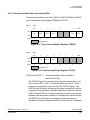
10.3 Overview. . . . . . . . . . . . . . . . . . . . . . . . . . . . . . . . . . . . . . . . . 210
10.3.1 Multiplexer . . . . . . . . . . . . . . . . . . . . . . . . . . . . . . . . . . . . .210
10.3.2 Analog Converter . . . . . . . . . . . . . . . . . . . . . . . . . . . . . . . . 212
10.3.3 Digital Control. . . . . . . . . . . . . . . . . . . . . . . . . . . . . . . . . . . 212
10.3.4 Result Registers . . . . . . . . . . . . . . . . . . . . . . . . . . . . . . . . .212
10.3.5 A/D Converter Clocks . . . . . . . . . . . . . . . . . . . . . . . . . . . . . 213
10.3.6 Conversion Sequence . . . . . . . . . . . . . . . . . . . . . . . . . . . . 213
10.4
A/D Converter Power-Up and Clock Select . . . . . . . . . . . . . . 214
10.5
Conversion Process . . . . . . . . . . . . . . . . . . . . . . . . . . . . . . . .215
10.6
Channel Assignments. . . . . . . . . . . . . . . . . . . . . . . . . . . . . . . 216
10.7
Single-Channel Operation . . . . . . . . . . . . . . . . . . . . . . . . . . . 216
10.8
Multiple-Channel Operation . . . . . . . . . . . . . . . . . . . . . . . . . . 217
10.9
Operation in Stop and Wait Modes. . . . . . . . . . . . . . . . . . . . . 217
10.10 A/D Control/Status Register . . . . . . . . . . . . . . . . . . . . . . . . . . 218
10.11 A/D Converter Result Registers . . . . . . . . . . . . . . . . . . . . . . .220
M68HC11E Family — Rev. 3.2
MOTOROLA
Technical Data
Table of Contents
13
Table of Contents
Section 11. Electrical Characteristics
11.1
Contents . . . . . . . . . . . . . . . . . . . . . . . . . . . . . . . . . . . . . . . . . 221
11.2
Introduction . . . . . . . . . . . . . . . . . . . . . . . . . . . . . . . . . . . . . . . 222
11.3
Maximum Ratings for Standard
and Extended Voltage Devices . . . . . . . . . . . . . . . . . . . . . 222
11.4
Functional Operating Range. . . . . . . . . . . . . . . . . . . . . . . . . . 223
11.5
Thermal Characteristics . . . . . . . . . . . . . . . . . . . . . . . . . . . . . 223
11.6
DC Electrical Characteristics . . . . . . . . . . . . . . . . . . . . . . . . . 224
11.7
Supply Currents and Power Dissipation . . . . . . . . . . . . . . . . . 225
11.8
MC68L11E9 DC Electrical Characteristics . . . . . . . . . . . . . . . 226
11.9
MC68L11E9 Supply Currents and Power Dissipation . . . . . . 227
11.10 Control Timing . . . . . . . . . . . . . . . . . . . . . . . . . . . . . . . . . . . . 229
11.11 MC68L11E9 Control Timing . . . . . . . . . . . . . . . . . . . . . . . . . . 230
11.12 Peripheral Port Timing . . . . . . . . . . . . . . . . . . . . . . . . . . . . . . 235
11.13 MC68L11E9 Peripheral Port Timing . . . . . . . . . . . . . . . . . . . . 236
11.14 Analog-to-Digital Converter Characteristics . . . . . . . . . . . . . . 240
11.15 MC68L11E9 Analog-to-Digital Converter Characteristics. . . . 241
11.16 Expansion Bus Timing Characteristics . . . . . . . . . . . . . . . . . . 242
11.17 MC68L11E9 Expansion Bus Timing Characteristics . . . . . . . 244
11.18 Serial Peripheral Interface Timing Characteristics . . . . . . . . .246
11.19 MC68L11E9 Serial Peirpheral Interface Characteristics . . . .247
11.20 EEPROM Characteristics . . . . . . . . . . . . . . . . . . . . . . . . . . . 250
11.21 MC68L11E9 EEPROM Characteristics . . . . . . . . . . . . . . . . . 250
11.22 EPROM Characteristics . . . . . . . . . . . . . . . . . . . . . . . . . . . . . 251
Technical Data
14
M68HC11E Family — Rev. 3.2
Table of Contents
MOTOROLA
Table of Contents
Section 12. Mechanical Data
12.1
Contents . . . . . . . . . . . . . . . . . . . . . . . . . . . . . . . . . . . . . . . . . 253
12.2
Introduction . . . . . . . . . . . . . . . . . . . . . . . . . . . . . . . . . . . . . . . 253
12.3
52-Pin Plastic-Leaded Chip Carrier (Case 778) . . . . . . . . . . . 255
12.4
52-Pin Windowed Ceramic-Leaded
Chip Carrier (Case 778B) . . . . . . . . . . . . . . . . . . . . . . . . . 256
12.5
64-Pin Quad Flat Pack (Case 840C) . . . . . . . . . . . . . . . . . . . 257
12.6
52-Pin Thin Quad Flat Pack (Case 848D) . . . . . . . . . . . . . . . 258
12.7
56-Pin Dual in-Line Package (Case #859) . . . . . . . . . . . . . . . 259
12.8
48-Pin Plastic DIP (Case 767) . . . . . . . . . . . . . . . . . . . . . . . . 259
Section 13. Ordering Information
13.1
Contents . . . . . . . . . . . . . . . . . . . . . . . . . . . . . . . . . . . . . . . . . 261
13.2
Introduction . . . . . . . . . . . . . . . . . . . . . . . . . . . . . . . . . . . . . . . 261
13.3
Standard Device Ordering Information . . . . . . . . . . . . . . . . . . 262
13.4
Custom ROM Device Ordering Information . . . . . . . . . . . . . . 265
13.5
Extended Voltage Device Ordering Information
(3.0 Vdc to 5.5 Vdc) . . . . . . . . . . . . . . . . . . . . . . . . . . . . . . 267
Appendix A. Development Support
A.1
Contents . . . . . . . . . . . . . . . . . . . . . . . . . . . . . . . . . . . . . . . . . 269
A.2
Introduction . . . . . . . . . . . . . . . . . . . . . . . . . . . . . . . . . . . . . . . 269
A.3
Motorola M68HC11 E-Series Development Tools . . . . . . . . .270
A.4
EVS — Evaluation System . . . . . . . . . . . . . . . . . . . . . . . . . . . 270
A.5
Motorola Modular Development System (MMDS11) . . . . . . . 271
A.6
SPGMR11 — Serial Programmer for M68HC11 MCUs . . . . .273
Appendix B. EVBU Schematic
M68HC11EVBU Schematic. . . . . . . . . . . . . . . . . . . . . . . . . . . . . . . . 275
M68HC11E Family — Rev. 3.2
MOTOROLA
Technical Data
Table of Contents
15
Table of Contents
AN1060
AN1060 — M68HC11 Bootstrap Mode . . . . . . . . . . . . . . . . . . . . . . 277
EB184
EB184 — Enabling the Security Feature on the MC68HC711E9
Devices with PCbug11 on the M68HC711E9PGMR 323
EB188
EB188 — Enabling the Security Feature on M68HC811E2
Devices with PCbug11 on the M68HC711E9PGMR . . . . . . . . . 327
EB296
EB296 — Programming MC68HC711E9 Devices
with PCbug11 and the M68HC11EVBU . . . . . . . . . . . . . . . . . . . 331
Technical Data
16
M68HC11E Family — Rev. 3.2
Table of Contents
MOTOROLA
Technical Data — M68HC11E Family
List of Figures
Figure
Title
1-1
M68HC11 E-Series Block Diagram . . . . . . . . . . . . . . . . . . . . 26
2-1
2-2
2-3
2-4
2-5
2-6
2-7
2-8
2-9
Pin Assignments for 52-Pin PLCC and CLCC . . . . . . . . . . . . 28
Pin Assignments for 64-Pin QFP . . . . . . . . . . . . . . . . . . . . . . 29
Pin Assignments for 52-Pin TQFP . . . . . . . . . . . . . . . . . . . . . 30
Pin Assignments for 56-Pin SDIP. . . . . . . . . . . . . . . . . . . . . . 31
Pin Assignments for 48-Pin DIP (MC68HC811E2). . . . . . . . . 32
External Reset Circuit. . . . . . . . . . . . . . . . . . . . . . . . . . . . . . . 33
External Reset Circuit with Delay . . . . . . . . . . . . . . . . . . . . . . 33
Common Parallel Resonant Crystal Connections . . . . . . . . . 35
External Oscillator Connections . . . . . . . . . . . . . . . . . . . . . . . 35
3-1
3-2
Programming Model . . . . . . . . . . . . . . . . . . . . . . . . . . . . . . . . 47
Stacking Operations . . . . . . . . . . . . . . . . . . . . . . . . . . . . . . . . 49
4-1
4-2
4-3
4-4
4-5
4-6
4-7
4-8
4-9
Address/Data Demultiplexing . . . . . . . . . . . . . . . . . . . . . . . . . 68
Memory Map for MC68HC11E0 . . . . . . . . . . . . . . . . . . . . . . . 70
Memory Map for MC68HC11E1 . . . . . . . . . . . . . . . . . . . . . . . 70
Memory Map for MC68HC(7)11E9. . . . . . . . . . . . . . . . . . . . . 71
Memory Map for MC68HC(7)11E20. . . . . . . . . . . . . . . . . . . .71
Memory Map for MC68HC811E2 . . . . . . . . . . . . . . . . . . . . . . 72
Register and Control Bit Assignments . . . . . . . . . . . . . . . . . . 72
RAM Standby MODB/VSTBY Connections . . . . . . . . . . . . . . . 81
Highest Priority I-Bit Interrupt and Miscellaneous
Register (HPRIO) . . . . . . . . . . . . . . . . . . . . . . . . . . . . . . . 83
System Configuration Register (CONFIG) . . . . . . . . . . . . . . .87
MC68HC811E2 System Configuration
Register (CONFIG) . . . . . . . . . . . . . . . . . . . . . . . . . . . . . . 87
RAM and I/O Mapping Register (INIT) . . . . . . . . . . . . . . . . . . 89
4-10
4-11
4-12
M68HC11E Family — Rev. 3.2
MOTOROLA
Page
Technical Data
List of Figures
17
List of Figures
Figure
4-13
4-14
4-15
4-16
4-17
5-1
5-2
5-3
5-4
Title
System Configuration Options Register (OPTION) . . . . . . . . 91
EPROM and EEPROM Programming
Control Register (PPROG) . . . . . . . . . . . . . . . . . . . . . . . .95
MC68HC711E20 EPROM Programming
Control Register (EPROG) . . . . . . . . . . . . . . . . . . . . . . . .96
Block Protect Register (BPROT) . . . . . . . . . . . . . . . . . . . . . . 99
EPROM and EEPROM Programming
Control Register (PPROG) . . . . . . . . . . . . . . . . . . . . . . .101
5-5
5-6
5-7
Arm/Reset COP Timer Circuitry Register (COPRST). . . . . . 111
System Configuration Options Register (OPTION) . . . . . . . 112
Configuration Control Register (CONFIG) . . . . . . . . . . . . . . 113
Highest Priority I-Bit Interrupt
and Miscellaneous Register (HPRIO) . . . . . . . . . . . . . . . 119
Processing Flow Out of Reset . . . . . . . . . . . . . . . . . . . . . . .125
Interrupt Priority Resolution . . . . . . . . . . . . . . . . . . . . . . . . . 127
Interrupt Source Resolution Within SCI . . . . . . . . . . . . . . . . 129
6-1
6-2
6-3
6-4
6-5
6-6
6-7
6-8
6-9
6-10
Port A Data Register (PORTA). . . . . . . . . . . . . . . . . . . . . . .134
Pulse Accumulator Control Register (PACTL) . . . . . . . . . . . 135
Port B Data Register (PORTB). . . . . . . . . . . . . . . . . . . . . . .136
Port C Data Register (PORTC) . . . . . . . . . . . . . . . . . . . . . . 136
Port C Latched Register (PORTCL) . . . . . . . . . . . . . . . . . . .137
Port C Data Direction Register (DDRC) . . . . . . . . . . . . . . . . 137
Port D Data Register (PORTD) . . . . . . . . . . . . . . . . . . . . . . 138
Port D Data Direction Register (DDRD) . . . . . . . . . . . . . . . . 138
Port E Data Register (PORTE). . . . . . . . . . . . . . . . . . . . . . .139
Parallel I/O Control Register (PIOC). . . . . . . . . . . . . . . . . . .141
7-1
7-2
7-3
7-4
7-5
7-6
7-7
SCI Transmitter Block Diagram . . . . . . . . . . . . . . . . . . . . . . 147
SCI Receiver Block Diagram . . . . . . . . . . . . . . . . . . . . . . . . 149
Serial Communications Data Register (SCDR) . . . . . . . . . . 152
Serial Communications Control Register 1 (SCCR1) . . . . . . 153
Serial Communications Control Register 2 (SCCR2) . . . . . . 154
Serial Communications Status Register (SCSR) . . . . . . . . .155
Baud Rate Register (BAUD). . . . . . . . . . . . . . . . . . . . . . . . . 157
Technical Data
18
Page
M68HC11E Family — Rev. 3.2
List of Figures
MOTOROLA
List of Figures
Figure
7-8
7-9
Title
7-10
SCI Baud Rate Generator Block Diagram . . . . . . . . . . . . . . 160
MC68HC(7)11E20 SCI Baud Rate
Generator Block Diagram . . . . . . . . . . . . . . . . . . . . . . . . 161
Interrupt Source Resolution Within SCI . . . . . . . . . . . . . . . . 163
8-1
8-2
8-3
8-4
8-5
SPI Block Diagram . . . . . . . . . . . . . . . . . . . . . . . . . . . . . . . . 167
SPI Transfer Format . . . . . . . . . . . . . . . . . . . . . . . . . . . . . . . 168
Serial Peripheral Control Register (SPCR). . . . . . . . . . . . . .173
Serial Peripheral Status Register (SPSR) . . . . . . . . . . . . . . 175
Serial Peripheral Data I/O Register (SPDR). . . . . . . . . . . . . 176
9-1
9-2
9-3
9-4
9-5
9-6
9-7
Timer Clock Divider Chains . . . . . . . . . . . . . . . . . . . . . . . . . 179
Capture/Compare Block Diagram. . . . . . . . . . . . . . . . . . . . . 181
Timer Control Register 2 (TCTL2) . . . . . . . . . . . . . . . . . . . . 183
Timer Input Capture 1 Register Pair (TIC1) . . . . . . . . . . . . . 184
Timer Input Capture 2 Register Pair (TIC2) . . . . . . . . . . . . . 185
Timer Input Capture 3 Register Pair (TIC3) . . . . . . . . . . . . . 185
Timer Input Capture 4/Output
Compare 5 Register Pair (TI4/O5). . . . . . . . . . . . . . . . . . 186
Timer Output Compare 1 Register Pair (TOC1) . . . . . . . . . . 188
Timer Output Compare 2 Register Pair (TOC2) . . . . . . . . . . 188
Timer Output Compare 3 Register Pair (TOC3) . . . . . . . . . . 189
Timer Output Compare 4 Register Pair (TOC4) . . . . . . . . . . 189
Timer Compare Force Register (CFORC) . . . . . . . . . . . . . . 190
Output Compare 1 Mask Register (OC1M) . . . . . . . . . . . . . 191
Output Compare 1 Data Register (OC1D) . . . . . . . . . . . . . . 192
Timer Counter Register (TCNT) . . . . . . . . . . . . . . . . . . . . . . 193
Timer Control Register 1 (TCTL1) . . . . . . . . . . . . . . . . . . . . 194
Timer Interrupt Mask 1 Register (TMSK1) . . . . . . . . . . . . . . 195
Timer Interrupt Flag 1 Register (TFLG1) . . . . . . . . . . . . . . . 196
Timer Interrupt Mask 2 Register (TMSK2) . . . . . . . . . . . . . . 196
Timer Interrupt Flag 2 Register (TFLG2) . . . . . . . . . . . . . . . 198
Timer Interrupt Mask 2 Register (TMSK2) . . . . . . . . . . . . . . 200
Timer Interrupt Flag 2 Register (TFLG2) . . . . . . . . . . . . . . . 201
Pulse Accumulator Control Register (PACTL) . . . . . . . . . . . 202
Pulse Accumulator . . . . . . . . . . . . . . . . . . . . . . . . . . . . . . . .204
9-8
9-9
9-10
9-11
9-12
9-13
9-14
9-15
9-16
9-17
9-18
9-19
9-20
9-21
9-22
9-23
9-24
M68HC11E Family — Rev. 3.2
MOTOROLA
Page
Technical Data
List of Figures
19
List of Figures
Figure
Title
9-25
9-26
9-27
9-28
Pulse Accumulator Control Register (PACTL) . . . . . . . . . . . 205
Pulse Accumulator Count Register (PACNT) . . . . . . . . . . . . 206
Timer Interrupt Mask 2 Register (TMSK2) . . . . . . . . . . . . . . 207
Timer Interrupt Flag 2 Register (TFLG2) . . . . . . . . . . . . . . . 207
10-1
10-2
10-3
10-4
10-5
10-6
A/D Converter Block Diagram . . . . . . . . . . . . . . . . . . . . . . .211
Electrical Model of an A/D Input Pin (Sample Mode) . . . . . . 211
A/D Conversion Sequence . . . . . . . . . . . . . . . . . . . . . . . . . . 213
System Configuration Options Register (OPTION) . . . . . . . 214
A/D Control/Status Register (ADCTL) . . . . . . . . . . . . . . . . . 218
Analog-to-Digital Converter
Result Registers (ADR1–ADR4) . . . . . . . . . . . . . . . . . . . 220
11-1
11-2
11-3
11-4
11-5
11-6
11-7
11-8
11-9
11-10
11-11
11-12
11-13
11-14
11-15
Test Methods . . . . . . . . . . . . . . . . . . . . . . . . . . . . . . . . . . . . 228
Timer Inputs . . . . . . . . . . . . . . . . . . . . . . . . . . . . . . . . . . . . .230
POR External Reset Timing Diagram. . . . . . . . . . . . . . . . . . 231
STOP Recovery Timing Diagram . . . . . . . . . . . . . . . . . . . . . 232
WAIT Recovery from Interrupt Timing Diagram . . . . . . . . . . 233
Interrupt Timing Diagram . . . . . . . . . . . . . . . . . . . . . . . . . . . 234
Port Read Timing Diagram . . . . . . . . . . . . . . . . . . . . . . . . . . 237
Port Write Timing Diagram . . . . . . . . . . . . . . . . . . . . . . . . . . 237
Simple Input Strobe Timing Diagram . . . . . . . . . . . . . . . . . .237
Simple Output Strobe Timing Diagram. . . . . . . . . . . . . . . . . 238
Port C Input Handshake Timing Diagram. . . . . . . . . . . . . . . 238
Port C Output Handshake Timing Diagram . . . . . . . . . . . . . 238
3-State Variation of Output Handshake Timing Diagram
(STRA Enables Output Buffer) . . . . . . . . . . . . . . . . . . . . 239
Multiplexed Expansion Bus Timing Diagram . . . . . . . . . . . . 245
SPI Timing Diagram . . . . . . . . . . . . . . . . . . . . . . . . . . . . . . . 248
B-1
EVBU Schematic Diagram . . . . . . . . . . . . . . . . . . . . . . . . . . 276
Technical Data
20
Page
M68HC11E Family — Rev. 3.2
List of Figures
MOTOROLA
Technical Data — M68HC11E Family
List of Tables
Table
Title
2-1
Port Signal Functions . . . . . . . . . . . . . . . . . . . . . . . . . . . . . . . . 40
3-1
3-2
Reset Vector Comparison. . . . . . . . . . . . . . . . . . . . . . . . . . . . .50
Instruction Set. . . . . . . . . . . . . . . . . . . . . . . . . . . . . . . . . . . . . .57
4-1
4-2
4-3
4-4
4-5
4-6
4-7
4-8
Hardware Mode Select Summary. . . . . . . . . . . . . . . . . . . . . . . 82
Write Access Limited Registers . . . . . . . . . . . . . . . . . . . . . . . .85
EEPROM Mapping . . . . . . . . . . . . . . . . . . . . . . . . . . . . . . . . . .88
RAM Mapping . . . . . . . . . . . . . . . . . . . . . . . . . . . . . . . . . . . . . .90
Register Mapping . . . . . . . . . . . . . . . . . . . . . . . . . . . . . . . . . . . 90
EEPROM Block Protect . . . . . . . . . . . . . . . . . . . . . . . . . . . . . 100
EEPROM Block Protect in MC68HC811E2 MCUs . . . . . . . . .100
EEPROM Erase . . . . . . . . . . . . . . . . . . . . . . . . . . . . . . . . . . . 102
5-1
5-2
5-3
5-4
5-5
COP Timer Rate Select . . . . . . . . . . . . . . . . . . . . . . . . . . . . . 110
Reset Cause, Reset Vector, and Operating Mode . . . . . . . . .114
Highest Priority Interrupt Selection . . . . . . . . . . . . . . . . . . . . . 120
Interrupt and Reset Vector Assignments . . . . . . . . . . . . . . . . 121
Stacking Order on Entry to Interrupts . . . . . . . . . . . . . . . . . . .122
6-1
6-2
Input/Output Ports. . . . . . . . . . . . . . . . . . . . . . . . . . . . . . . . . . 133
Parallel I/O Control . . . . . . . . . . . . . . . . . . . . . . . . . . . . . . . . .143
7-1
Baud Rate Values. . . . . . . . . . . . . . . . . . . . . . . . . . . . . . . . . . 158
8-1
SPI Clock Rates . . . . . . . . . . . . . . . . . . . . . . . . . . . . . . . . . . . 174
9-1
9-2
Timer Summary . . . . . . . . . . . . . . . . . . . . . . . . . . . . . . . . . . . 180
Timer Control Configuration . . . . . . . . . . . . . . . . . . . . . . . . . . 183
M68HC11E Family — Rev. 3.2
MOTOROLA
Page
Technical Data
List of Tables
21
List of Tables
Table
Title
9-3
9-4
9-5
9-6
9-7
Timer Output Compare Actions . . . . . . . . . . . . . . . . . . . . . . .194
Timer Prescale . . . . . . . . . . . . . . . . . . . . . . . . . . . . . . . . . . . . 197
RTI Rates . . . . . . . . . . . . . . . . . . . . . . . . . . . . . . . . . . . . . . . . 199
Pulse Accumulator Timing . . . . . . . . . . . . . . . . . . . . . . . . . . . 204
Pulse Accumulator Edge Control . . . . . . . . . . . . . . . . . . . . . . 205
10-1
10-2
Converter Channel Assignments . . . . . . . . . . . . . . . . . . . . . . 216
A/D Converter Channel Selection. . . . . . . . . . . . . . . . . . . . . . 219
Technical Data
22
Page
M68HC11E Family — Rev. 3.2
List of Tables
MOTOROLA
Technical Data — M68HC11E Family
Section 1. General Description
1.1 Contents
1.2
Introduction . . . . . . . . . . . . . . . . . . . . . . . . . . . . . . . . . . . . . . . . 23
1.3
Features . . . . . . . . . . . . . . . . . . . . . . . . . . . . . . . . . . . . . . . . . . 24
1.4
Structure . . . . . . . . . . . . . . . . . . . . . . . . . . . . . . . . . . . . . . . . . . 25
1.2 Introduction
This document contains a detailed description of the M68HC11 E series
of 8-bit microcontroller units (MCUs). These MCUs all combine the
M68HC11 central processor unit (CPU) with high-performance, on-chip
peripherals.
The E series is comprised of many devices with various
configurations of:
•
Random-access memory (RAM)
•
Read-only memory (ROM)
•
Erasable programmable read-only memory (EPROM)
•
Electrically erasable programmable read-only memory
(EEPROM)
•
Several low-voltage devices are also available.
With the exception of a few minor differences, the operation of all
E-series MCUs is identical. A fully static design and high-density
complementary metal-oxide semiconductor (HCMOS) fabrication
process allow the E-series devices to operate at frequencies from 3 MHz
to dc with very low power consumption.
M68HC11E Family — Rev. 3.2
MOTOROLA
Technical Data
General Description
23
General Description
1.3 Features
Features of the E-series devices include:
•
M68HC11 CPU
•
Power-saving stop and wait modes
•
Low-voltage devices available (3.0–5.5 Vdc)
•
0, 256, 512, or 768 bytes of on-chip RAM, data retained during
standby
•
0, 12, or 20 Kbytes of on-chip ROM or EPROM
•
0, 512, or 2048 bytes of on-chip EEPROM with block protect for
security
•
2048 bytes of EEPROM with selectable base address in the
MC68HC811E2
•
Asynchronous non-return-to-zero (NRZ) serial communications
interface (SCI)
•
Additional baud rates available on MC68HC(7)11E20
•
Synchronous serial peripheral interface (SPI)
•
8-channel, 8-bit analog-to-digital (A/D) converter
•
16-bit timer system:
– Three input capture (IC) channels
– Four output compare (OC) channels
– One additional channel, selectable as fourth IC or fifth OC
•
8-bit pulse accumulator
•
Real-time interrupt circuit
•
Computer operating properly (COP) watchdog system
•
38 general-purpose input/output (I/O) pins:
– 16 bidirectional I/O pins
– 11 input-only pins
– 11 output-only pins
Technical Data
24
M68HC11E Family — Rev. 3.2
General Description
MOTOROLA
General Description
Structure
•
Several packaging options:
– 52-pin plastic-leaded chip carrier (PLCC)
– 52-pin windowed ceramic leaded chip carrier (CLCC)
– 52-pin plastic thin quad flat pack, 10 mm x 10 mm (TQFP)
– 64-pin quad flat pack (QFP)
– 48-pin plastic dual in-line package (DIP), MC68HC811E2 only
– 56-pin plastic shrink dual in-line package, .070-inch lead
spacing (SDIP)
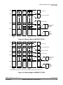
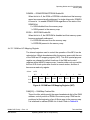
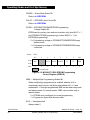
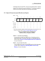
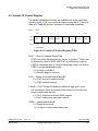
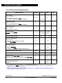
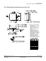
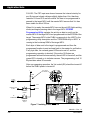
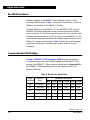
1.4 Structure
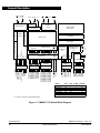
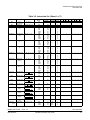
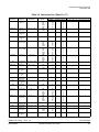
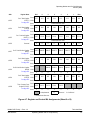
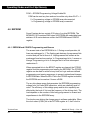
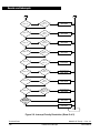
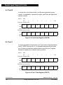
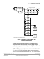
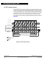
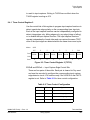
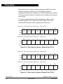
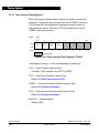
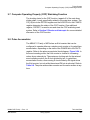
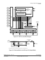
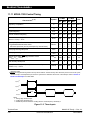
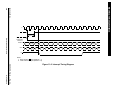
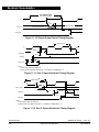
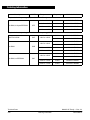
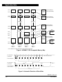
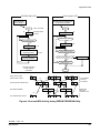
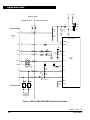
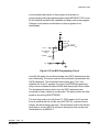
See Figure 1-1 for a functional diagram of the E-series MCUs.
Differences among devices are noted in the table accompanying
Figure 1-1.
M68HC11E Family — Rev. 3.2
MOTOROLA
Technical Data
General Description
25
General Description
XTAL EXTAL
E
IRQ
OSC
INTERRUPT
LOGIC
MODE CONTROL
ROM OR EPROM
(SEE TABLE)
EEPROM
(SEE TABLE)
M68HC11 CPU
RAM
(SEE TABLE)
STROBE AND HANDSHAKE
PARALLEL I/O
SERIAL
COMMUNICATION
INTERFACE
SCI
SERIAL
PERIPHERAL
INTERFACE
SPI
VDD
VSS
VRH
VRL
TxD
RxD
ADDRESS/DATA
SS
SCK
MOSI
MISO
BUS EXPANSION
ADDRESS
R/W
AS
PULSE ACCUMULATOR
COP
PAI
OC2
OC3
OC4
OC5/IC4/OC1
IC1
IC2
PERIODIC INTERRUPT
IC3
CLOCK LOGIC
TIMER
SYSTEM
XIRQ/VPPE* RESET
STRB
STRA
MODA/ MODB/
LIR
VSTBY
A/D CONVERTER
DEVICE
MC68HC11E0
MC68HC11E1
MC68HC11E9
MC68HC711E9
MC68HC11E20
MC68HC711E20
MC68HC811E2
RAM
512
512
512
512
768
768
256
ROM
—
—
12 K
—
20 K
—
—
PE7/AN7
PE6/AN6
PE5/AN5
PE4/AN4
PE3/AN3
PE2/AN2
PE1/AN1
PE0/AN0
PORT E
PD5/SS
PD4/SCK
PD3/MOSI
PD2/MISO
PD1/TxD
PD0/RxD
STRA/AS
PORT C
STRB/R/W
PORT B
PC7/ADDR7/DATA7
PC6/ADDR6/DATA6
PC5/ADDR5/DATA5
PC4/ADDR4/DATA4
PC3/ADDR3/DATA3
PC2/ADDR2/DATA2
PC1/ADDR1/DATA1
PC0/ADDR0/DATA0
PORT D
PORT A
PB7/ADDR15
PB6/ADDR14
PB5/ADDR13
PB4/ADDR12
PB3/ADDR11
PB2/ADDR10
PB1/ADDR9
PB0/ADDR8
CONTROL
PA7/PAI
PA6/OC2/OC1
PA5/OC3/OC1
PA4/OC4/OC1
PA3/OC5/IC4/OC1
PA2/IC1
PA1/IC2
PA0/IC3
CONTROL
EPROM
—
—
—
12 K
—
20 K
—
EEPROM
—
512
512
512
512
512
2048
* VPPE applies only to devices with EPROM/OTPROM.
Figure 1-1. M68HC11 E-Series Block Diagram
Technical Data
26
M68HC11E Family — Rev. 3.2
General Description
MOTOROLA
Technical Data — M68HC11E Family
Section 2. Pin Descriptions
2.1 Contents
2.2
Introduction . . . . . . . . . . . . . . . . . . . . . . . . . . . . . . . . . . . . . . . . 28
2.3
VDD and VSS . . . . . . . . . . . . . . . . . . . . . . . . . . . . . . . . . . . . . . . 32
2.4
RESET . . . . . . . . . . . . . . . . . . . . . . . . . . . . . . . . . . . . . . . . . . . 34
2.5
Crystal Driver and External Clock Input
(XTAL and EXTAL) . . . . . . . . . . . . . . . . . . . . . . . . . . . . . . . 35
2.6
E-Clock Output (E) . . . . . . . . . . . . . . . . . . . . . . . . . . . . . . . . . . 36
2.7
Interrupt Request (IRQ) . . . . . . . . . . . . . . . . . . . . . . . . . . . . . . 36
2.8
Non-Maskable Interrupt (XIRQ/VPPE). . . . . . . . . . . . . . . . . . . .36
2.9
MODA and MODB (MODA/LIR and MODB/VSTBY) . . . . . . . . . 37
2.10
VRL and VRH . . . . . . . . . . . . . . . . . . . . . . . . . . . . . . . . . . . . . . . 38
2.11
STRA/AS . . . . . . . . . . . . . . . . . . . . . . . . . . . . . . . . . . . . . . . . . 38
2.12
STRB/R/W . . . . . . . . . . . . . . . . . . . . . . . . . . . . . . . . . . . . . . . . 38
2.13 Port Signals . . . . . . . . . . . . . . . . . . . . . . . . . . . . . . . . . . . . . . . 39
2.13.1 Port A . . . . . . . . . . . . . . . . . . . . . . . . . . . . . . . . . . . . . . . . . . 39
2.13.2 Port B . . . . . . . . . . . . . . . . . . . . . . . . . . . . . . . . . . . . . . . . . . 41
2.13.3 Port C . . . . . . . . . . . . . . . . . . . . . . . . . . . . . . . . . . . . . . . . . . 42
2.13.4 Port D . . . . . . . . . . . . . . . . . . . . . . . . . . . . . . . . . . . . . . . . . . 43
2.13.5 Port E . . . . . . . . . . . . . . . . . . . . . . . . . . . . . . . . . . . . . . . . . . 43
M68HC11E Family — Rev. 3.2
MOTOROLA
Technical Data
Pin Descriptions
27
Pin Descriptions
2.2 Introduction
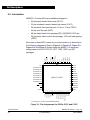
M68HC11 E-series MCUs are available packaged in:
•
52-pin plastic-leaded chip carrier (PLCC)
•
52-pin windowed ceramic leaded chip carrier (CLCC)
•
52-pin plastic thin quad flat pack, 10 mm x 10 mm (TQFP)
•
64-pin quad flat pack (QFP)
•
48-pin plastic dual in-line package (DIP), MC68HC811E2 only
•
56-pin plastic shrink dual in-line package, .070-inch lead spacing
(SDIP)
47 PE2/AN2
48 PE6/AN6
49 PE3/AN3
50 PE7/AN7
51 VRL
VSS
52 VRH
2 MODB/VSTBY
3 MODA/LIR
4 STRA/AS
5 E
6 STRB/R/W
7 EXTAL
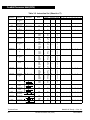
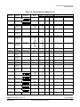
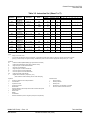
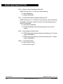
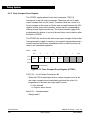
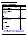
Most pins on these MCUs serve two or more functions, as described in
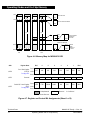
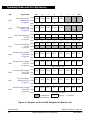
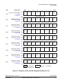
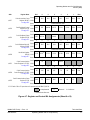
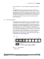
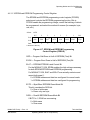
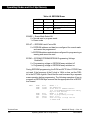
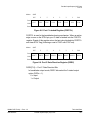
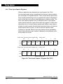
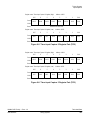
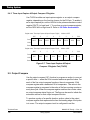
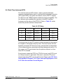
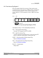
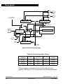
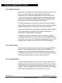
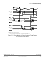
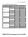
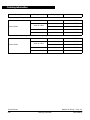
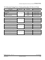
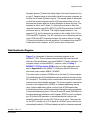
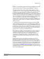
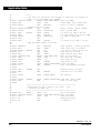
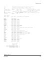
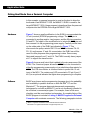
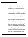
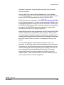
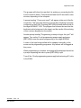
the following paragraphs. Refer to Figure 2-1, Figure 2-2, Figure 2-3,
Figure 2-4, and Figure 2-5 which show the M68HC11 E-series pin
assignments for the PLCC/CLCC, QFP, TQFP, SDIP, and DIP
packages.
PE5/AN5
9
45
PE1/AN1
10
44
PE4/AN4
PC2/ADDR2/DATA2
11
43
PE0/AN0
PC3/ADDR3/DATA3
12
42
PB0/ADDR8
PC4/ADDR4/DATA4
13
41
PB1/ADDR9
PC5/ADDR5/DATA5
14
40
PB2/ADDR10
PC6/ADDR6/DATA6
15
39
PB3/ADDR11
PC7/ADDR7/DATA7
16
38
PB4/ADDR12
8
PC0/ADDR0/DATA0
PC1/ADDR1/DATA1
1
46
XTAL
M68HC11 E SERIES
31
32
33
PA3/OC5/IC4/OC1
PA2/IC1
PA1/IC2
29
30
28
PA5/OC3/OC1
* VPPE applies only to devices with EPROM/OTPROM.
PA4/OC4/OC1
27
PA7/PAI/OC1
PA6/OC2/OC1
PA0/IC3
26
34
25
20
PD5/SS
VDD
PD0/RxD
24
PB7/ADDR15
23
35
PD4/SCK
IRQ
PD3/MOSI
PB6/ADDR14
19
22
PB5/ADDR13
36
21
37
18
PD1/TxD
17
PD2/MISO
RESET
* XIRQ/VPPE
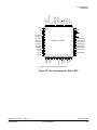
Figure 2-1. Pin Assignments for 52-Pin PLCC and CLCC
Technical Data
28
M68HC11E Family — Rev. 3.2
Pin Descriptions
MOTOROLA
PA0/IC3
NC
NC
NC
PB7/ADDR15
PB6/ADDR14
PB5/ADDR13
PB4/ADDR12
1
PB3/ADDR11
PB2/ADDR10
PB1/ADDR9
PB0/ADDR8
PE0/AN0
PE4/AN4
PE1/AN1
PE5/AN5
9
10
11
12
13
14
15
16
56
55
54
53
52
51
50
49
64
63
62
61
60
59
58
57
PA1/IC2
PA2/IC1
PA3/OC5/IC4/OC1
NC
NC
PA4/OC4/OC1
PA5/OC3/OC1
PA6/OC2/OC1
PA7/PAI/OC1
VDD
PD5/SS
PD4/SCK
PD3/MOSI
PD2/MISO
PD1/TxD
VSS
Pin Descriptions
Introduction
2
3
M68HC11 E SERIES
NC
PD0/RxD
IRQ
XIRQ/VPPE*
NC
RESET
PC7/ADDR7/DATA7
PC6/ADDR6/DATA6
PC5/ADDR5/DATA5
PC4/ADDR4/DATA4
PC3/ADDR3/DATA3
PC2/ADDR2/DATA2
PC1/ADDR1/DATA1
NC
PC0/ADDR0/DATA0
XTAL
PE2/AN2
PE6/AN6
PE3/AN3
PE7/AN7
VRL
VRH
VSS
VSS
MODB/VSTBY
NC
MODA/LIR
STRA/AS
E
STRB/R/W
EXTAL
NC
17
18
19
20
21
22
23
24
25
26
27
28
29
30
31
32
4
5
6
7
8
48
47
46
45
44
43
42
41
40
39
38
37
36
35
34
33
* VPPE applies only to devices with EPROM/OTPROM.
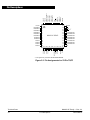
Figure 2-2. Pin Assignments for 64-Pin QFP
M68HC11E Family — Rev. 3.2
MOTOROLA
Technical Data
Pin Descriptions
29
1
2
3
4
5
6
7
8
9
10
11
12
13
39
38
37
36
35
34
33
32
31
30
29
28
27
PD0/RxD
IRQ
XIRQ/VPPE*
RESET
PC7/ADDR7/DATA7
PC6/ADDR6/DATA6
PC5/ADDR5/DATA5
PC4/ADDR4/DATA4
PC3/ADDR3/DATA3
PC2/ADDR2/DATA2
PC1/ADDR1/DATA1
PC0/ADDR0/DATA0
XTAL
PE2/AN2
PE6/AN6
PE3/AN3
PE7/AN7
VRL
VRH
VSS
MODB/VSTBY
MODA/LIR
STRA/AS
E
STRB/R/W
EXTAL
19
20
21
22
23
24
25
26
M68HC11 E SERIES
14
15
16
17
18
PA0/IC3
PB7/ADDR15
PB6/ADDR14
PB5/ADDR13
PB4/ADDR12
PB3/ADDR11
PB2/ADDR10
PB1/ADDR9
PB0/ADDR8
PE0/AN0
PE4/AN4
PE1/AN1
PE5/AN5
45
44
43
42
41
40
52
51
50
49
48
47
46
PA1/IC2
PA2/IC1
PA3/OC5/IC4/OC1
PA4/OC4/OC1
PA5/OC3/OC1
PA6/OC2/OC1
PA7/PAI/OC1
VDD
PD5/SS
PD4/SCK
PD3/MOSI
PD2/MISO
PD1/TxD
Pin Descriptions
* VPPE applies only to devices with EPROM/OTPROM.
Figure 2-3. Pin Assignments for 52-Pin TQFP
Technical Data
30
M68HC11E Family — Rev. 3.2
Pin Descriptions
MOTOROLA
Pin Descriptions
Introduction
VSS
1
56
EVSS
MODB/VSTBY
2
55
VRH
MODA/LIR
3
54
VRL
STRA/AS
4
53
PE7/AN7
E
5
52
PE3/AN3
STRB/R/W
6
51
PE6/AN6
EXTAL
7
50
PE2/AN2
XTAL
8
49
PE5/AN5
PC0/ADDR0/DATA0
9
48
PE1/AN1
PC1/ADDR1/DATA1
10
47
PE4/AN4
PC2/ADDR2/DATA2
11
46
PE0/AN0
PC3/ADDR3/DATA3
12
45
PB0/ADDR8
PC4/ADDR4/DATA4
13
44
PB1/ADDR9
PC5/ADDR5/DATA5
14
43
PB2/ADDR10
PC6/ADDR6/DATA6
15
M68HC11 E SERIES 42
PB3/ADDR11
PC7/ADDR7/DATA7
16
41
PB4/ADDR12
RESET
17
40
PB5/ADDR13
* XIRQ/VPPE
18
39
PB6/ADDR14
IRQ
19
38
PB7/ADDR15
PD0/RxD
20
37
PA0/IC3
EVSS
21
36
PA1/IC2
PD1/TxD
22
35
PA2/IC1
PD2/MISO
23
34
PA3/OC5/IC4/OC1
PD3/MOSI
24
33
PA4/OC4/OC1
PD4/SCK
25
32
PA5/OC3/OC1
PD5/SS
26
31
PA6/OC2/OC1
VDD
27
30
PA7/PAI/OC1
VSS
28
29
EVDD
* V PPE applies only to devices with EPROM/OTPROM.
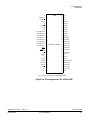
Figure 2-4. Pin Assignments for 56-Pin SDIP
M68HC11E Family — Rev. 3.2
MOTOROLA
Technical Data
Pin Descriptions
31
Pin Descriptions
PA7/PAI/OC1
1
48
VDD
PA6/OC2/OC1
2
47
PD5/SS
PA5/OC3/OC1
3
46
PD4/SCK
PA4/OC4/OC1
4
45
PD3/MOSI
PA3/OC5/IC4/OC1
5
44
PD2/MISO
PA2/IC1
6
43
PD1/TxD
PA1/IC2
7
42
PD0/RxD
PA0/IC3
8
41
IRQ
PB7/ADDR15
9
40
XIRQ
PB6/ADDR14
10
39
RESET
PB5/ADDR13
11
PB4/ADDR12
12
PB3/ADDR11
38
PC7/ADDR7/DATA7
37
PC6/ADDR6/DATA6
13
36
PC5/ADDR5/DATA5
PB2/ADDR10
14
35
PC4/ADDR4/DATA4
PB1/ADDR9
15
34
PC3/ADDR3/DATA3
PB0/ADDR8
16
33
PC2/ADDR2/DATA2
PE0/AN0
MC68HC811E2
17
32
PC1/ADDR1/DATA1
PE1/AN1
18
31
PC0/ADDR0/DATA0
PE2/AN2
19
30
XTAL
PE3/AN3
20
29
EXTAL
VRL
21
28
STRB/R/W
VRH
22
27
E
VSS
23
26
STRA/AS
MODB/VSTBY
24
25
MODA/LIR
Figure 2-5. Pin Assignments for 48-Pin DIP (MC68HC811E2)
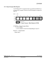
2.3 VDD and VSS
Power is supplied to the MCU through VDD and VSS. VDD is the power
supply, VSS is ground. The MCU operates from a single 5-volt (nominal)
power supply. Low-voltage devices in the E series operate at
3.0–5.5 volts.
Very fast signal transitions occur on the MCU pins. The short rise and fall
times place high, short duration current demands on the power supply.
To prevent noise problems, provide good power supply bypassing at the
MCU. Also, use bypass capacitors that have good
Technical Data
32
M68HC11E Family — Rev. 3.2
Pin Descriptions
MOTOROLA
Pin Descriptions
VDD and VSS
high-frequency characteristics and situate them as close to the MCU as
possible. Bypass requirements vary, depending on how heavily the MCU
pins are loaded.
VDD
VDD
2
4.7 kΩ
IN
RESET
MC34(0/1)64
1
TO RESET
OF M68HC11
GND
3
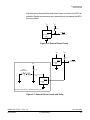
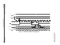
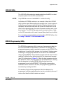
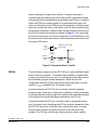
Figure 2-6. External Reset Circuit
VDD
VDD
IN
RESET
MC34064
GND
VDD
4.7 kΩ
TO RESET
OF M68HC11
4.7 k Ω
MANUAL
RESET SWITCH
4.7 kΩ
1.0 µF
IN
RESET
MC34164
GND
OPTIONAL POWER-ON DELAY AND MANUAL RESET SWITCH
Figure 2-7. External Reset Circuit with Delay
M68HC11E Family — Rev. 3.2
MOTOROLA
Technical Data
Pin Descriptions
33
Pin Descriptions
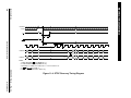
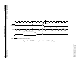
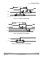
2.4 RESET
A bidirectional control signal, RESET, acts as an input to initialize the
MCU to a known startup state. It also acts as an open-drain output to
indicate that an internal failure has been detected in either the clock
monitor or computer operating properly (COP) watchdog circuit. The
CPU distinguishes between internal and external reset conditions by
sensing whether the reset pin rises to a logic 1 in less than two E-clock
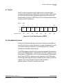
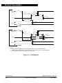
cycles after a reset has occurred. See Figure 2-6 and Figure 2-7.
CAUTION:
Do not connect an external resistor capacitor (RC) power-up delay
circuit to the reset pin of M68HC11 devices because the circuit charge
time constant can cause the device to misinterpret the type of reset that
occurred.
Because the CPU is not able to fetch and execute instructions properly
when VDD falls below the minimum operating voltage level, reset must
be controlled. A low-voltage inhibit (LVI) circuit is required primarily for
protection of EEPROM contents. However, since the configuration
register (CONFIG) value is read from the EEPROM, protection is
required even if the EEPROM array is not being used.
Presently, there are several economical ways to solve this problem. For
example, two good external components for LVI reset are:
1. The Seiko S0854HN (or other S805 series devices):
— Extremely low power (2 µA)
— TO-92 package
— Limited temperature range, –20°C to +70°C
— Available in various trip-point voltage ranges
2. The Motorola MC34064:
— TO-92 or SO-8 package
— Draws about 300 µA
— Temperature range –40°C to 85°C
— Well controlled trip point
— Inexpensive
Refer to Section 5. Resets and Interrupts for further information.
Technical Data
34
M68HC11E Family — Rev. 3.2
Pin Descriptions
MOTOROLA
Pin Descriptions
Crystal Driver and External Clock Input (XTAL and EXTAL)
2.5 Crystal Driver and External Clock Input (XTAL and EXTAL)
These two pins provide the interface for either a crystal or a CMOScompatible clock to control the internal clock generator circuitry. The
frequency applied to these pins is four times higher than the desired
E-clock rate.
The XTAL pin must be left unterminated when an external CMOScompatible clock input is connected to the EXTAL pin. The XTAL output
is normally intended to drive only a crystal.
CAUTION:
In all cases, use caution around the oscillator pins. Load capacitances
shown in the oscillator circuit are specified by the crystal manufacturer
and should include all stray layout capacitances.
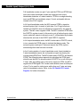
Refer to Figure 2-8 and Figure 2-9.
CL
EXTAL
10 MΩ
MCU
4xE
CRYSTAL
CL
XTAL
Figure 2-8. Common Parallel Resonant
Crystal Connections
4xE
CMOS-COMPATIBLE
EXTERNAL OSCILLATOR
EXTAL
MCU
XTAL
NC
Figure 2-9. External Oscillator Connections
M68HC11E Family — Rev. 3.2
MOTOROLA
Technical Data
Pin Descriptions
35
Pin Descriptions
2.6 E-Clock Output (E)
E is the output connection for the internally generated E clock. The signal
from E is used as a timing reference. The frequency of the E-clock output
is one fourth that of the input frequency at the XTAL and EXTAL pins.
When E-clock output is low, an internal process is taking place. When it
is high, data is being accessed.
All clocks, including the E clock, are halted when the MCU is in stop
mode. To reduce RFI emissions, the E-clock output of most E-series
devices can be disabled while operating in single-chip modes.
The E-clock signal is always enabled on the MC68HC811E2.
2.7 Interrupt Request (IRQ)
The IRQ input provides a means of applying asynchronous interrupt
requests to the MCU. Either negative edge-sensitive triggering or
level-sensitive triggering is program selectable (OPTION register). IRQ
is always configured to level-sensitive triggering at reset. When using
IRQ in a level-sensitive wired-OR configuration, connect an external
pullup resistor, typically 4.7 kΩ, to VDD.
2.8 Non-Maskable Interrupt (XIRQ/VPPE)
The XIRQ input provides a means of requesting a non-maskable
interrupt after reset initialization. During reset, the X bit in the condition
code register (CCR) is set and any interrupt is masked until MCU
software enables it. Because the XIRQ input is level-sensitive, it can be
connected to a multiple-source wired-OR network with an external pullup
resistor to VDD. XIRQ is often used as a power loss detect interrupt.
Whenever XIRQ or IRQ is used with multiple interrupt sources each
source must drive the interrupt input with an open-drain type of driver to
avoid contention between outputs.
NOTE:
IRQ must be configured for level-sensitive operation if there is more than
one source of IRQ interrupt.
Technical Data
36
M68HC11E Family — Rev. 3.2
Pin Descriptions
MOTOROLA
Pin Descriptions
MODA and MODB (MODA/LIR and MODB/VSTBY)
There should be a single pullup resistor near the MCU interrupt input pin
(typically 4.7 kΩ). There must also be an interlock mechanism at each
interrupt source so that the source holds the interrupt line low until the
MCU recognizes and acknowledges the interrupt request. If one or more
interrupt sources are still pending after the MCU services a request, the
interrupt line will still be held low and the MCU will be interrupted again
as soon as the interrupt mask bit in the MCU is cleared (normally upon
return from an interrupt). Refer to Section 5. Resets and Interrupts.
VPPE is the input for the 12-volt nominal programming voltage required
for EPROM/OTPROM programming. On devices without
EPROM/OTPROM, this pin is only an XIRQ input.
2.9 MODA and MODB (MODA/LIR and MODB/VSTBY)
During reset, MODA and MODB select one of the four operating modes:
•
Single-chip mode
•
Expanded mode
•
Test mode
•
Bootstrap mode
Refer to Section 4. Operating Modes and On-Chip Memory.
After the operating mode has been selected, the load instruction register
(LIR) pin provides an open-drain output to indicate that execution of an
instruction has begun. A series of E-clock cycles occurs during
execution of each instruction. The LIR signal goes low during the first
E-clock cycle of each instruction (opcode fetch). This output is provided
for assistance in program debugging.
The VSTBY pin is used to input random-access memory (RAM) standby
power. When the voltage on this pin is more than one MOS threshold
(about 0.7 volts) above the VDD voltage, the internal RAM and part of the
reset logic are powered from this signal rather than the VDD input. This
allows RAM contents to be retained without VDD power applied to the
MCU. Reset must be driven low before VDD is removed and must remain
low until VDD has been restored to a valid level.
M68HC11E Family — Rev. 3.2
MOTOROLA
Technical Data
Pin Descriptions
37
Pin Descriptions
2.10 VRL and VRH
These two inputs provide the reference voltages for the analog-to-digital
(A/D) converter circuitry:
•
VRL is the low reference, typically 0 Vdc.
•
VRH is the high reference.
For proper A/D converter operation:
•
VRH should be at least 3 Vdc greater than VRL.
•
VRL and VRH should be between VSS and VDD.
2.11 STRA/AS
The strobe A (STRA) and address strobe (AS) pin performs either of two
separate functions, depending on the operating mode:
•
In single-chip mode, STRA performs an input handshake (strobe
input) function.
•
In the expanded multiplexed mode, AS provides an address
strobe function.
AS can be used to demultiplex the address and data signals at port C.
Refer to Section 4. Operating Modes and On-Chip Memory.
2.12 STRB/R/W
The strobe B (STRB) and read/write (R/W) pin act as either an output
strobe or as a data bus direction indicator, depending on the operating
mode.
In single-chip operating mode, STRB acts as a programmable strobe for
handshake with other parallel devices. Refer to Section 6. Parallel
Input/Output (I/O) Ports for further information.
In expanded multiplexed operating mode, R/W is used to indicate the
direction of transfers on the external data bus. A low on the R/W pin
indicates data is being written to the external data bus. A high on this pin
Technical Data
38
M68HC11E Family — Rev. 3.2
Pin Descriptions
MOTOROLA
Pin Descriptions
Port Signals
indicates that a read cycle is in progress. R/W stays low during
consecutive data bus write cycles, such as a double-byte store. It is
possible for data to be driven out of port C, if internal read visibility (IRV)
is enabled and an internal address is read, even though R/W is in a
high-impedance state. Refer to Section 4. Operating Modes and
On-Chip Memory for more information about IRVNE (internal read
visibility not E).
2.13 Port Signals
Port pins have different functions in different operating modes. Pin
functions for port A, port D, and port E are independent of operating
modes. Port B and port C, however, are affected by operating mode.
Port B provides eight general-purpose output signals in single-chip
operating modes. When the microcontroller is in expanded multiplexed
operating mode, port B pins are the eight high-order address lines.
Port C provides eight general-purpose input/output signals when the
MCU is in the single-chip operating mode. When the microcontroller is in
the expanded multiplexed operating mode, port C pins are a multiplexed
address/data bus.
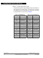
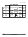
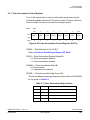
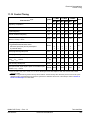
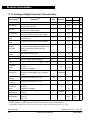
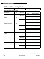
Refer to Table 2-1 for a functional description of the 40 port signals
within different operating modes. Terminate unused inputs and
input/output (I/O) pins configured as inputs high or low.
2.13.1 Port A
In all operating modes, port A can be configured for three timer input
capture (IC) functions and four timer output compare (OC) functions. An
additional pin can be configured as either the fourth IC or the fifth OC.
Any port A pin that is not currently being used for a timer function can be
used as either a general-purpose input or output line. Only port A pins
PA7 and PA3 have an associated data direction control bit that allows
the pin to be selectively configured as input or output. Bits DDRA7 and
DDRA3 located in PACTL register control data direction for PA7 and
PA3, respectively. All other port A pins are fixed as either input or output.
M68HC11E Family — Rev. 3.2
MOTOROLA
Technical Data
Pin Descriptions
39
Pin Descriptions
Table 2-1. Port Signal Functions
Port/Bit
PA0
PA1
PA2
PA3
PA4
PA5
PA6
PA7
PB0
PB1
PB2
PB3
PB4
PB5
PB6
PB7
PC0
PC1
PC2
PC3
PC4
PC5
PC6
PC7
PD0
PD1
PD2
PD3
PD4
PD5
—
—
PE0
PE1
PE2
PE3
PE4
PE5
PE6
PE7
Single-Chip and
Bootstrap Modes
PA0/IC3
PA1/IC2
PA2/IC1
PA3/OC5/IC4/OC1
PA4/OC4/OC1
PA5/OC3/OC1
PA6/OC2/OC1
PA7/PAI/OC1
PB0
PB1
PB2
PB3
PB4
PB5
PB6
PB7
PC0
PC1
PC2
PC3
PC4
PC5
PC6
PC7
ADDR8
ADDR9
ADDR10
ADDR11
ADDR12
ADDR13
ADDR14
ADDR15
ADDR0/DATA0
ADDR1/DATA1
ADDR2/DATA2
ADDR3/DATA3
ADDR4/DATA4
ADDR5/DATA5
ADDR6/DATA6
ADDR7/DATA7
PD0/RxD
PD1/TxD
PD2/MISO
PD3/MOSI
PD4/SCK
PD5/SS
STRA
STRB
AS
R/W
PE0/AN0
PE1/AN1
PE3/AN2
PE3/AN3
PE4/AN4
PE5/AN5
PE6/AN6
PE7/AN7
Technical Data
40
Expanded and
Test Modes
M68HC11E Family — Rev. 3.2
Pin Descriptions
MOTOROLA
Pin Descriptions
Port Signals
PA7 can function as general-purpose I/O or as timer output compare for
OC1. PA7 is also the input to the pulse accumulator, even while
functioning as a general-purpose I/O or an OC1 output.
PA6–PA4 serve as either general-purpose outputs, timer input captures,
or timer output compare 2–4. In addition, PA6–PA4 can be controlled by
OC1.
PA3 can be a general-purpose I/O pin or a timer IC/OC pin. Timer
functions associated with this pin include OC1 and IC4/OC5. IC4/OC5 is
software selectable as either a fourth input capture or a fifth output
compare. PA3 can also be configured to allow OC1 edges to trigger IC4
captures.
PA2–PA0 serve as general-purpose inputs or as IC1–IC3.
PORTA can be read at any time. Reads of pins configured as inputs
return the logic level present on the pin. Pins configured as outputs
return the logic level present at the pin driver input. If written, PORTA
stores the data in an internal latch, bits 7 and 3. It drives the pins only if
they are configured as outputs. Writes to PORTA do not change the pin
state when pins are configured for timer input captures or output
compares. Refer to Section 6. Parallel Input/Output (I/O) Ports.
2.13.2 Port B
During single-chip operating modes, all port B pins are general-purpose
output pins. During MCU reads of this port, the level sensed at the input
side of the port B output drivers is read. Port B can also be used in simple
strobed output mode. In this mode, an output pulse appears at the STRB
signal each time data is written to port B.
In expanded multiplexed operating modes, all of the port B pins act as
high order address output signals. During each MCU cycle, bits 15–8 of
the address bus are output on the PB7–PB0 pins. The PORTB register
is treated as an external address in expanded modes.
M68HC11E Family — Rev. 3.2
MOTOROLA
Technical Data
Pin Descriptions
41
Pin Descriptions
2.13.3 Port C
While in single-chip operating modes, all port C pins are
general-purpose I/O pins. Port C inputs can be latched into an alternate
PORTCL register by providing an input transition to the STRA signal.
Port C can also be used in full handshake modes of parallel I/O where
the STRA input and STRB output act as handshake control lines.
When in expanded multiplexed modes, all port C pins are configured as
multiplexed address/data signals. During the address portion of each
MCU cycle, bits 7–0 of the address are output on the PC7–PC0 pins.
During the data portion of each MCU cycle (E high), PC7–PC0 are
bidirectional data signals, DATA7–DATA0. The direction of data at the
port C pins is indicated by the R/W signal.
The CWOM control bit in the PIOC register disables the port C P-channel
output driver. CWOM simultaneously affects all eight bits of port C.
Because the N-channel driver is not affected by CWOM, setting CWOM
causes port C to become an open-drain type output port suitable for
wired-OR operation.
In wired-OR mode:
•
When a port C bit is at logic level 0, it is driven low by the
N-channel driver.
•
When a port C bit is at logic level 1, the associated pin has
high-impedance, as neither the N-channel nor the P-channel
devices are active.
It is customary to have an external pullup resistor on lines that are driven
by open-drain devices. Port C can only be configured for wired-OR
operation when the MCU is in single-chip mode. Refer to Section 6.
Parallel Input/Output (I/O) Ports for additional information about port C
functions.
Technical Data
42
M68HC11E Family — Rev. 3.2
Pin Descriptions
MOTOROLA
Pin Descriptions
Port Signals
2.13.4 Port D
Pins PD5–PD0 can be used for general-purpose I/O signals. These pins
alternately serve as the serial communication interface (SCI) and serial
peripheral interface (SPI) signals when those subsystems are enabled.
•
PD0 is the receive data input (RxD) signal for the SCI.
•
PD1 is the transmit data output (TxD) signal for the SCI.
•
PD5–PD2 are dedicated to the SPI:
– PD2 is the master in/slave out (MISO) signal.
– PD3 is the master out/slave in (MOSI) signal.
– PD4 is the serial clock (SCK) signal.
– PD5 is the slave select (SS) input.
2.13.5 Port E
Use port E for general-purpose or analog-to-digital (A/D) inputs.
CAUTION:
If high accuracy is required for A/D conversions, avoid reading port E
during sampling, as small disturbances can reduce the accuracy of that
result.
M68HC11E Family — Rev. 3.2
MOTOROLA
Technical Data
Pin Descriptions
43
Pin Descriptions
Technical Data
44
M68HC11E Family — Rev. 3.2
Pin Descriptions
MOTOROLA
Technical Data — M68HC11E Family
Section 3. Central Processor Unit (CPU)
3.1 Contents
3.2
Introduction . . . . . . . . . . . . . . . . . . . . . . . . . . . . . . . . . . . . . . . . 46
3.3
CPU Registers . . . . . . . . . . . . . . . . . . . . . . . . . . . . . . . . . . . . . 46
3.3.1
Accumulators A, B, and D . . . . . . . . . . . . . . . . . . . . . . . . . . 47
3.3.2
Index Register X (IX) . . . . . . . . . . . . . . . . . . . . . . . . . . . . . . 48
3.3.3
Index Register Y (IY) . . . . . . . . . . . . . . . . . . . . . . . . . . . . . . 48
3.3.4
Stack Pointer (SP) . . . . . . . . . . . . . . . . . . . . . . . . . . . . . . . . 48
3.3.5
Program Counter (PC) . . . . . . . . . . . . . . . . . . . . . . . . . . . . .50
3.3.6
Condition Code Register (CCR) . . . . . . . . . . . . . . . . . . . . . . 51
3.3.6.1
Carry/Borrow (C) . . . . . . . . . . . . . . . . . . . . . . . . . . . . . . . 51
3.3.6.2
Overflow (V) . . . . . . . . . . . . . . . . . . . . . . . . . . . . . . . . . . . 51
3.3.6.3
Zero (Z) . . . . . . . . . . . . . . . . . . . . . . . . . . . . . . . . . . . . . .51
3.3.6.4
Negative (N) . . . . . . . . . . . . . . . . . . . . . . . . . . . . . . . . . . . 52
3.3.6.5
Interrupt Mask (I) . . . . . . . . . . . . . . . . . . . . . . . . . . . . . . . 52
3.3.6.6
Half Carry (H) . . . . . . . . . . . . . . . . . . . . . . . . . . . . . . . . . .52
3.3.6.7
X Interrupt Mask (X) . . . . . . . . . . . . . . . . . . . . . . . . . . . . .52
3.3.6.8
STOP Disable (S) . . . . . . . . . . . . . . . . . . . . . . . . . . . . . . 53
3.4
Data Types . . . . . . . . . . . . . . . . . . . . . . . . . . . . . . . . . . . . . . . . 53
3.5
Opcodes and Operands . . . . . . . . . . . . . . . . . . . . . . . . . . . . . . 53
3.6
Addressing Modes . . . . . . . . . . . . . . . . . . . . . . . . . . . . . . . . . . 54
3.6.1
Immediate. . . . . . . . . . . . . . . . . . . . . . . . . . . . . . . . . . . . . . . 54
3.6.2
Direct . . . . . . . . . . . . . . . . . . . . . . . . . . . . . . . . . . . . . . . . . . 55
3.6.3
Extended . . . . . . . . . . . . . . . . . . . . . . . . . . . . . . . . . . . . . . . 55
3.6.4
Indexed. . . . . . . . . . . . . . . . . . . . . . . . . . . . . . . . . . . . . . . . . 55
3.6.5
Inherent . . . . . . . . . . . . . . . . . . . . . . . . . . . . . . . . . . . . . . . . 55
3.6.6
Relative . . . . . . . . . . . . . . . . . . . . . . . . . . . . . . . . . . . . . . . . 56
3.7
Instruction Set. . . . . . . . . . . . . . . . . . . . . . . . . . . . . . . . . . . . . .56
M68HC11E Family — Rev. 3.2
MOTOROLA
Technical Data
Central Processor Unit (CPU)
45
Central Processor Unit (CPU)
3.2 Introduction
This section presents information on M68HC11:
•
Central processor unit (CPU) architecture
•
Data types
•
Addressing modes
•
Instruction set
•
Special operations such as subroutine calls and interrupts
The CPU is designed to treat all peripheral, input/output (I/O), and
memory locations identically as addresses in the 64-Kbyte memory map.
This is referred to as memory-mapped I/O. There are no special
instructions for I/O that are separate from those used for memory. This
architecture also allows accessing an operand from an external memory
location with no execution time penalty.
3.3 CPU Registers
M68HC11 CPU registers are an integral part of the CPU and are not
addressed as if they were memory locations. The seven registers,
discussed in the following paragraphs, are shown in Figure 3-1.
Technical Data
46
M68HC11E Family — Rev. 3.2
Central Processor Unit (CPU)
MOTOROLA
Central Processor Unit (CPU)
CPU Registers
7
15
A
0
7
B
0
0
D
8-BIT ACCUMULATORS A & B
OR 16-BIT DOUBLE ACCUMULATOR D
IX
INDEX REGISTER X
IY
INDEX REGISTER Y
SP
STACK POINTER
PROGRAM COUNTER
PC
7
S
0
X
H
I
N
Z
V
C
CONDITION CODES
CARRY/BORROW FROM MSB
OVERFLOW
ZERO
NEGATIVE
I-INTERRUPT MASK
HALF CARRY (FROM BIT 3)
X-INTERRUPT MASK
STOP DISABLE
Figure 3-1. Programming Model
3.3.1 Accumulators A, B, and D
Accumulators A and B are general-purpose 8-bit registers that hold
operands and results of arithmetic calculations or data manipulations.
For some instructions, these two accumulators are treated as a single
double-byte (16-bit) accumulator called accumulator D. Although most
instructions can use accumulators A or B interchangeably, these
exceptions apply:
•
The ABX and ABY instructions add the contents of 8-bit
accumulator B to the contents of 16-bit register X or Y, but there
are no equivalent instructions that use A instead of B.
•
The TAP and TPA instructions transfer data from accumulator A
to the condition code register or from the condition code register
to accumulator A. However, there are no equivalent instructions
that use B rather than A.
M68HC11E Family — Rev. 3.2
MOTOROLA
Technical Data
Central Processor Unit (CPU)
47
Central Processor Unit (CPU)
•
The decimal adjust accumulator A (DAA) instruction is used after
binary-coded decimal (BCD) arithmetic operations, but there is no
equivalent BCD instruction to adjust accumulator B.
•
The add, subtract, and compare instructions associated with both
A and B (ABA, SBA, and CBA) only operate in one direction,
making it important to plan ahead to ensure that the correct
operand is in the correct accumulator.
3.3.2 Index Register X (IX)
The IX register provides a 16-bit indexing value that can be added to the
8-bit offset provided in an instruction to create an effective address. The
IX register can also be used as a counter or as a temporary storage
register.
3.3.3 Index Register Y (IY)
The 16-bit IY register performs an indexed mode function similar to that
of the IX register. However, most instructions using the IY register
require an extra byte of machine code and an extra cycle of execution
time because of the way the opcode map is implemented. Refer to
3.5 Opcodes and Operands for further information.
3.3.4 Stack Pointer (SP)
The M68HC11 CPU has an automatic program stack. This stack can be
located anywhere in the address space and can be any size up to the
amount of memory available in the system. Normally, the SP is initialized
by one of the first instructions in an application program. The stack is
configured as a data structure that grows downward from high memory
to low memory. Each time a new byte is pushed onto the stack, the SP
is decremented. Each time a byte is pulled from the stack, the SP is
incremented. At any given time, the SP holds the 16-bit address of the
next free location in the stack. Figure 3-2 is a summary of SP
operations.
Technical Data
48
M68HC11E Family — Rev. 3.2
Central Processor Unit (CPU)
MOTOROLA
Central Processor Unit (CPU)
CPU Registers
JSR, JUMP TO SUBROUTINE
RTI, RETURN FROM INTERRUPT
MAIN PROGRAM
INTERRUPT ROUTINE
PC
PC
DIRECT
$9D = JSR
dd
RTN NEXT MAIN INSTR.
$3B = RTI
SP+2
SP+3
SP+4
PC
$AD = JSR
ff
RTN NEXT MAIN INSTR.
SP+5
7
0
SP+6
➩ SP–2
SP+7
SP
PC
$18 = PRE
$AD = JSR
RTN
ff
NEXT MAIN INSTR.
SP+8
RTNH
RTNL
SP–1
MAIN PROGRAM
INDEXED, Y
STACK
➩ SP+9
MAIN PROGRAM
PC
$3F = SWI
SP–6
WAI, WAIT FOR INTERRUPT
$8D = BSR
7
STACK
SP–3
$3E = WAI
SP–2
SP
7
STACK
SP
SP+1
➩ SP+2
CCR
ACCB
ACCA
IXH
IXL
IYH
IYL
RTNH
RTNL
LEGEND:
RTNH
RTNL
SP
RTS, RETURN FROM
SUBROUTINE
MAIN PROGRAM
0
0
➩ SP–2
$39 = RTS
SP–4
SP–1
SP–1
PC
SP–5
MAIN PROGRAM
BSR, BRANCH TO SUBROUTINE
STACK
➩ SP–9
SP–7
$BD = PRE
hh
RTN
ll
NEXT MAIN INSTR.
PC
PC
7
SP–8
MAIN PROGRAM
MAIN PROGRAM
0
SWI, SOFTWARE INTERRUPT
PC
INDEXED, Y
STACK
CCR
ACCB
ACCA
IXH
IXL
IYH
IYL
RTNH
RTNL
SP+1
MAIN PROGRAM
INDEXED, X
7
SP
RTNH
RTNL
0
RTN = ADDRESS OF NEXT INSTRUCTION IN MAIN PROGRAM TO
BE EXECUTED UPON RETURN FROM SUBROUTINE
RTNH = MOST SIGNIFICANT BYTE OF RETURN ADDRESS
RTNL = LEAST SIGNIFICANT BYTE OF RETURN ADDRESS
➩ = STACK POINTER POSITION AFTER OPERATION IS COMPLETE
dd = 8-BIT DIRECT ADDRESS ($0000–$00FF) (HIGH BYTE ASSUMED
TO BE $00)
ff = 8-BIT POSITIVE OFFSET $00 (0) TO $FF (255) IS ADDED TO INDEX
hh = HIGH-ORDER BYTE OF 16-BIT EXTENDED ADDRESS
ll = LOW-ORDER BYTE OF 16-BIT EXTENDED ADDRESS
rr= SIGNED RELATIVE OFFSET $80 (–128) TO $7F (+127) (OFFSET
RELATIVE TO THE ADDRESS FOLLOWING THE MACHINE CODE
OFFSET BYTE)
Figure 3-2. Stacking Operations
When a subroutine is called by a jump-to-subroutine (JSR) or branch-tosubroutine (BSR) instruction, the address of the instruction after the JSR
or BSR is automatically pushed onto the stack, least significant byte first.
When the subroutine is finished, a return-from-subroutine (RTS)
instruction is executed. The RTS pulls the previously stacked return
address from the stack and loads it into the program counter. Execution
then continues at this recovered return address.
M68HC11E Family — Rev. 3.2
MOTOROLA
Technical Data
Central Processor Unit (CPU)
49
Central Processor Unit (CPU)
When an interrupt is recognized, the current instruction finishes
normally, the return address (the current value in the program counter)
is pushed onto the stack, all of the CPU registers are pushed onto the
stack, and execution continues at the address specified by the vector for
the interrupt.
At the end of the interrupt service routine, an return-from interrupt (RTI)
instruction is executed. The RTI instruction causes the saved registers
to be pulled off the stack in reverse order. Program execution resumes
at the return address.
Certain instructions push and pull the A and B accumulators and the X
and Y index registers and are often used to preserve program context.
For example, pushing accumulator A onto the stack when entering a
subroutine that uses accumulator A and then pulling accumulator A off
the stack just before leaving the subroutine ensures that the contents of
a register will be the same after returning from the subroutine as it was
before starting the subroutine.
3.3.5 Program Counter (PC)
The program counter, a 16-bit register, contains the address of the next
instruction to be executed. After reset, the program counter is initialized
from one of six possible vectors, depending on operating mode and the
cause of reset. See Table 3-1.
Table 3-1. Reset Vector Comparison
Mode
POR or RESET Pin
Clock Monitor
COP Watchdog
Normal
$FFFE, F
$FFFC, D
$FFFA, B
Test or Boot
$BFFE, F
$BFFC, D
$BFFA, B
Technical Data
50
M68HC11E Family — Rev. 3.2
Central Processor Unit (CPU)
MOTOROLA
Central Processor Unit (CPU)
CPU Registers
3.3.6 Condition Code Register (CCR)
This 8-bit register contains:
•
Five condition code indicators (C, V, Z, N, and H),
•
Two interrupt masking bits (IRQ and XIRQ)
•
A stop disable bit (S)
In the M68HC11 CPU, condition codes are updated automatically by
most instructions. For example, load accumulator A (LDAA) and store
accumulator A (STAA) instructions automatically set or clear the N, Z,
and V condition code flags. Pushes, pulls, add B to X (ABX), add B to Y
(ABY), and transfer/exchange instructions do not affect the condition
codes. Refer to Table 3-2, which shows what condition codes are
affected by a particular instruction.
3.3.6.1 Carry/Borrow (C)
The C bit is set if the arithmetic logic unit (ALU) performs a carry or
borrow during an arithmetic operation. The C bit also acts as an error flag
for multiply and divide operations. Shift and rotate instructions operate
with and through the carry bit to facilitate multiple-word shift operations.
3.3.6.2 Overflow (V)
The overflow bit is set if an operation causes an arithmetic overflow.
Otherwise, the V bit is cleared.
3.3.6.3 Zero (Z)
The Z bit is set if the result of an arithmetic, logic, or data manipulation
operation is 0. Otherwise, the Z bit is cleared. Compare instructions do
an internal implied subtraction and the condition codes, including Z,
reflect the results of that subtraction. A few operations (INX, DEX, INY,
and DEY) affect the Z bit and no other condition flags. For these
operations, only = and ≠ conditions can be determined.
M68HC11E Family — Rev. 3.2
MOTOROLA
Technical Data
Central Processor Unit (CPU)
51
Central Processor Unit (CPU)
3.3.6.4 Negative (N)
The N bit is set if the result of an arithmetic, logic, or data manipulation
operation is negative (MSB = 1). Otherwise, the N bit is cleared. A result
is said to be negative if its most significant bit (MSB) is a 1. A quick way
to test whether the contents of a memory location has the MSB set is to
load it into an accumulator and then check the status of the N bit.
3.3.6.5 Interrupt Mask (I)
The interrupt request (IRQ) mask (I bit) is a global mask that disables all
maskable interrupt sources. While the I bit is set, interrupts can become
pending, but the operation of the CPU continues uninterrupted until the
I bit is cleared. After any reset, the I bit is set by default and can only be
cleared by a software instruction. When an interrupt is recognized, the I
bit is set after the registers are stacked, but before the interrupt vector is
fetched. After the interrupt has been serviced, a return-from-interrupt
instruction is normally executed, restoring the registers to the values that
were present before the interrupt occurred. Normally, the I bit is 0 after
a return from interrupt is executed. Although the I bit can be cleared
within an interrupt service routine, "nesting" interrupts in this way should
only be done when there is a clear understanding of latency and of the
arbitration mechanism. Refer to Section 5. Resets and Interrupts.
3.3.6.6 Half Carry (H)
The H bit is set when a carry occurs between bits 3 and 4 of the
arithmetic logic unit during an ADD, ABA, or ADC instruction. Otherwise,
the H bit is cleared. Half carry is used during BCD operations.
3.3.6.7 X Interrupt Mask (X)
The XIRQ mask (X) bit disables interrupts from the XIRQ pin. After any
reset, X is set by default and must be cleared by a software instruction.
When an XIRQ interrupt is recognized, the X and I bits are set after the
registers are stacked, but before the interrupt vector is fetched. After the
interrupt has been serviced, an RTI instruction is normally executed,
causing the registers to be restored to the values that were present
before the interrupt occurred. The X interrupt mask bit is set only by
Technical Data
52
M68HC11E Family — Rev. 3.2
Central Processor Unit (CPU)
MOTOROLA
Central Processor Unit (CPU)
Data Types
hardware (RESET or XIRQ acknowledge). X is cleared only by program
instruction (TAP, where the associated bit of A is 0; or RTI, where bit 6
of the value loaded into the CCR from the stack has been cleared).
There is no hardware action for clearing X.
3.3.6.8 STOP Disable (S)
Setting the STOP disable (S) bit prevents the STOP instruction from
putting the M68HC11 into a low-power stop condition. If the STOP
instruction is encountered by the CPU while the S bit is set, it is treated
as a no-operation (NOP) instruction, and processing continues to the
next instruction. S is set by reset; STOP is disabled by default.
3.4 Data Types
The M68HC11 CPU supports four data types:
1. Bit data
2. 8-bit and 16-bit signed and unsigned integers
3. 16-bit unsigned fractions
4. 16-bit addresses
A byte is eight bits wide and can be accessed at any byte location. A
word is composed of two consecutive bytes with the most significant
byte at the lower value address. Because the M68HC11 is an 8-bit CPU,
there are no special requirements for alignment of instructions or
operands.
3.5 Opcodes and Operands
The M68HC11 Family of microcontrollers uses 8-bit opcodes. Each
opcode identifies a particular instruction and associated addressing
mode to the CPU. Several opcodes are required to provide each
instruction with a range of addressing capabilities. Only 256 opcodes
would be available if the range of values were restricted to the number
able to be expressed in 8-bit binary numbers.
M68HC11E Family — Rev. 3.2
MOTOROLA
Technical Data
Central Processor Unit (CPU)
53
Central Processor Unit (CPU)
A 4-page opcode map has been implemented to expand the number of
instructions. An additional byte, called a prebyte, directs the processor
from page 0 of the opcode map to one of the other three pages. As its
name implies, the additional byte precedes the opcode.
A complete instruction consists of a prebyte, if any, an opcode, and zero,
one, two, or three operands. The operands contain information the CPU
needs for executing the instruction. Complete instructions can be from
one to five bytes long.
3.6 Addressing Modes
Six addressing modes can be used to access memory:
•
Immediate
•
Direct
•
Extended
•
Indexed
•
Inherent
•
Relative
These modes are detailed in the following paragraphs. All modes except
inherent mode use an effective address. The effective address is the
memory address from which the argument is fetched or stored or the
address from which execution is to proceed. The effective address can
be specified within an instruction, or it can be calculated.
3.6.1 Immediate
In the immediate addressing mode, an argument is contained in the
byte(s) immediately following the opcode. The number of bytes following
the opcode matches the size of the register or memory location being
operated on. There are 2-, 3-, and 4- (if prebyte is required) byte
immediate instructions. The effective address is the address of the byte
following the instruction.
Technical Data
54
M68HC11E Family — Rev. 3.2
Central Processor Unit (CPU)
MOTOROLA
Central Processor Unit (CPU)
Addressing Modes
3.6.2 Direct
In the direct addressing mode, the low-order byte of the operand
address is contained in a single byte following the opcode, and the
high-order byte of the address is assumed to be $00. Addresses
$00–$FF are thus accessed directly, using 2-byte instructions.
Execution time is reduced by eliminating the additional memory access
required for the high-order address byte. In most applications, this
256-byte area is reserved for frequently referenced data. In M68HC11
MCUs, the memory map can be configured for combinations of internal
registers, RAM, or external memory to occupy these addresses.
3.6.3 Extended
In the extended addressing mode, the effective address of the argument
is contained in two bytes following the opcode byte. These are 3-byte
instructions (or 4-byte instructions if a prebyte is required). One or two
bytes are needed for the opcode and two for the effective address.
3.6.4 Indexed
In the indexed addressing mode, an 8-bit unsigned offset contained in
the instruction is added to the value contained in an index register (IX or
IY). The sum is the effective address. This addressing mode allows
referencing any memory location in the 64-Kbyte address space. These
are 2- to 5-byte instructions, depending on whether or not a prebyte is
required.
3.6.5 Inherent
In the inherent addressing mode, all the information necessary to
execute the instruction is contained in the opcode. Operations that use
only the index registers or accumulators, as well as control instructions
with no arguments, are included in this addressing mode. These are
1- or 2-byte instructions.
M68HC11E Family — Rev. 3.2
MOTOROLA
Technical Data
Central Processor Unit (CPU)
55
Central Processor Unit (CPU)
3.6.6 Relative
The relative addressing mode is used only for branch instructions. If the
branch condition is true, an 8-bit signed offset included in the instruction
is added to the contents of the program counter to form the effective
branch address. Otherwise, control proceeds to the next instruction.
These are usually 2-byte instructions.
3.7 Instruction Set
Refer to Table 3-2, which shows all the M68HC11 instructions in all
possible addressing modes. For each instruction, the table shows the
operand construction, the number of machine code bytes, and execution
time in CPU E-clock cycles.
Technical Data
56
M68HC11E Family — Rev. 3.2
Central Processor Unit (CPU)
MOTOROLA
Central Processor Unit (CPU)
Instruction Set
Table 3-2. Instruction Set (Sheet 1 of 7)
Mnemonic
Operation
Description
ABA
Add
Accumulators
Add B to X
Add B to Y
Add with Carry
to A
A+B⇒A
ABX
ABY
ADCA (opr)
Addressing
Mode
INH
IX + (00 : B) ⇒ IX
IY + (00 : B) ⇒ IY
A+M+C⇒A
ADCB (opr)
Add with Carry
to B
B+M+C⇒B
ADDA (opr)
Add Memory to
A
A+M⇒A
ADDB (opr)
Add Memory to
B
B+M⇒B
ADDD (opr)
Add 16-Bit to D
D + (M : M + 1) ⇒ D
ANDA (opr)
AND A with
Memory
A•M⇒A
ANDB (opr)
AND B with
Memory
B•M⇒B
ASL (opr)
Arithmetic Shift
Left
C
ASLA
0
b0
b7
b0
b7
18
18
18
18
18
18
18
18
18
Instruction
Operand
—
3A
3A
89
99
B9
A9
A9
C9
D9
F9
E9
E9
8B
9B
BB
AB
AB
CB
DB
FB
EB
EB
C3
D3
F3
E3
E3
84
94
B4
A4
A4
C4
D4
F4
E4
E4
78
68
68
—
—
ii
dd
hh ll
ff
ff
ii
dd
hh ll
ff
ff
ii
dd
hh ll
ff
ff
ii
dd
hh ll
ff
ff
jj kk
dd
hh ll
ff
ff
ii
dd
hh ll
ff
ff
ii
dd
hh ll
ff
ff
hh ll
ff
ff
Cycles
2
S
—
X
—
Condition Codes
H
I
N
Z
∆
—
∆
∆
V
∆
C
∆
3
4
2
3
4
4
5
2
3
4
4
5
2
3
4
4
5
2
3
4
4
5
4
5
6
6
7
2
3
4
4
5
2
3
4
4
5
6
6
7
—
—
—
—
—
—
—
—
∆
—
—
—
—
—
∆
—
—
∆
—
—
∆
—
—
∆
—
—
∆
—
∆
∆
∆
∆
—
—
∆
—
∆
∆
∆
∆
—
—
∆
—
∆
∆
∆
∆
—
—
—
—
∆
∆
∆
∆
—
—
—
—
∆
∆
0
—
—
—
—
—
∆
∆
0
—
—
—
—
—
∆
∆
∆
∆
A
INH
48
—
2
—
—
—
—
∆
∆
∆
∆
B
INH
58
—
2
—
—
—
—
∆
∆
∆
∆
INH
05
—
3
—
—
—
—
∆
∆
∆
∆
77
67
67
47
hh ll
ff
ff
—
6
6
7
2
—
—
—
—
∆
∆
∆
∆
A
EXT
IND,X
IND,Y
INH
—
—
—
—
∆
∆
∆
∆
B
INH
57
—
2
—
—
—
—
∆
∆
∆
∆
REL
24
rr
3
—
—
—
—
—
—
—
—
DIR
IND,X
IND,Y
15
1D
1D
dd mm
ff mm
ff mm
6
7
8
—
—
—
—
∆
∆
0
—
0
Arithmetic Shift
Left B
C
ASLD
A
A
A
A
A
B
B
B
B
B
Arithmetic Shift
Left A
C
ASLB
b7
A
A
A
A
A
B
B
B
B
B
A
A
A
A
A
B
B
B
B
B
INH
INH
IMM
DIR
EXT
IND,X
IND,Y
IMM
DIR
EXT
IND,X
IND,Y
IMM
DIR
EXT
IND,X
IND,Y
IMM
DIR
EXT
IND,X
IND,Y
IMM
DIR
EXT
IND,X
IND,Y
IMM
DIR
EXT
IND,X
IND,Y
IMM
DIR
EXT
IND,X
IND,Y
EXT
IND,X
IND,Y
Opcode
1B
0
b0
Arithmetic Shift
Left D
0
C b7 A b0 b7 B b0
ASR
Arithmetic Shift
Right
ASRA
Arithmetic Shift
Right A
ASRB
Arithmetic Shift
Right B
BCC (rel)
Branch if Carry
Clear
Clear Bit(s)
b7
b0
b7
b0
b7
BCLR (opr)
(msk)
b0
C
18
C
C
?C=0
M • (mm) ⇒ M
18
M68HC11E Family — Rev. 3.2
MOTOROLA
Technical Data
Central Processor Unit (CPU)
57
Central Processor Unit (CPU)
Table 3-2. Instruction Set (Sheet 2 of 7)
Mnemonic
Operation
Description
BCS (rel)
Branch if Carry
Set
Branch if = Zero
Branch if ∆ Zero
Branch if > Zero
Branch if
Higher
Branch if
Higher or Same
Bit(s) Test A
with Memory
?C=1
BEQ (rel)
BGE (rel)
BGT (rel)
BHI (rel)
BHS (rel)
BITA (opr)
—
—
—
—
—
—
—
—
—
—
—
—
—
—
—
—
—
—
—
—
?C=0
REL
24
rr
3
—
—
—
—
—
—
—
—
IMM
DIR
EXT
IND,X
IND,Y
IMM
DIR
EXT
IND,X
IND,Y
REL
REL
REL
85
95
B5
A5
A5
C5
D5
F5
E5
E5
2F
25
23
ii
dd
hh ll
ff
ff
ii
dd
hh ll
ff
ff
rr
rr
rr
2
3
4
4
5
2
3
4
4
5
3
3
3
—
—
—
—
∆
∆
0
—
—
—
—
—
∆
∆
0
—
—
—
—
—
—
—
—
—
—
—
—
—
—
—
—
—
—
—
—
—
—
—
—
—
REL
REL
REL
2D
2B
26
rr
rr
rr
3
3
3
—
—
—
—
—
—
—
—
—
—
—
—
—
—
—
—
—
—
—
—
—
—
—
—
REL
REL
DIR
IND,X
IND,Y
REL
DIR
IND,X
IND,Y
DIR
IND,X
IND,Y
REL
2A
20
13
1F
1F
21
12
1E
1E
14
1C
1C
8D
rr
rr
dd mm rr
ff mm rr
ff mm rr
rr
dd mm rr
ff mm rr
ff mm rr
dd mm
ff mm
ff mm
rr
3
3
6
7
8
3
6
7
8
6
7
8
6
—
—
—
—
—
—
—
—
—
—
—
—
—
—
—
—
—
—
—
—
—
—
—
—
—
—
—
—
—
—
—
—
—
—
—
—
—
—
—
—
—
—
—
—
∆
∆
0
—
—
—
—
—
—
—
—
—
A•M
Set Bit(s)
M + mm ⇒ M
Branch to
Subroutine
Branch if
Overflow Clear
Branch if
Overflow Set
Compare A to B
Clear Carry Bit
Clear Interrupt
Mask
Clear Memory
Byte
See Figure 3–2
Clear
Accumulator A
Clear
Accumulator B
Clear Overflow
Flag
Compare A to
Memory
0⇒A
0⇒B
CLRB
CLV
CMPA (opr)
A
A
A
A
A
B
B
B
B
B
?N⊕V=1
?N=1
?Z=0
?N=0
?1=1
? M • mm = 0
18
18
18
18
18
?V=0
REL
28
rr
3
—
—
—
—
—
—
—
—
?V=1
REL
29
rr
3
—
—
—
—
—
—
—
—
A–B
0⇒C
0⇒I
INH
INH
INH
11
0C
0E
—
—
—
2
2
2
—
—
—
—
—
—
—
—
—
—
—
0
∆
—
—
∆
—
—
∆
—
—
∆
0
—
0⇒M
7F
6F
6F
4F
hh ll
ff
ff
—
6
6
7
2
—
—
—
—
0
1
0
0
A
EXT
IND,X
IND,Y
INH
—
—
—
—
0
1
0
0
B
INH
5F
—
2
—
—
—
—
0
1
0
0
INH
0A
—
2
—
—
—
—
—
—
0
—
IMM
DIR
EXT
IND,X
IND,Y
81
91
B1
A1
A1
2
3
4
4
5
—
—
—
—
∆
∆
∆
∆
0⇒V
A–M
A
A
A
A
A
18
18
ii
dd
hh ll
ff
ff
Technical Data
58
C
—
—
—
—
—
?1=0
? (M) • mm = 0
CLRA
V
—
—
—
—
—
Branch Never
Branch if Bit(s)
Set
CLR (opr)
Condition Codes
H
I
N
Z
—
—
—
—
—
—
—
—
? Z + (N ⊕ V) = 1
?C=1
?C+Z=1
CBA
CLC
CLI
X
—
3
3
3
3
Branch if ∆ Zero
Branch if Lower
Branch if Lower
or Same
Branch if < Zero
Branch if Minus
Branch if not =
Zero
Branch if Plus
Branch Always
Branch if
Bit(s) Clear
BVS (rel)
S
—
rr
rr
rr
rr
BLE (rel)
BLO (rel)
BLS (rel)
BVC (rel)
Cycles
3
27
2C
2E
22
B•M
BSR (rel)
Instruction
Operand
rr
REL
REL
REL
REL
Bit(s) Test B
with Memory
BPL (rel)
BRA (rel)
BRCLR(opr)
(msk)
(rel)
BRN (rel)
BRSET(opr)
(msk)
(rel)
BSET (opr)
(msk)
Opcode
25
?Z=1
?N⊕V=0
? Z + (N ⊕ V) = 0
?C+Z=0
BITB (opr)
BLT (rel)
BMI (rel)
BNE (rel)
Addressing
Mode
REL
M68HC11E Family — Rev. 3.2
Central Processor Unit (CPU)
MOTOROLA
Central Processor Unit (CPU)
Instruction Set
Table 3-2. Instruction Set (Sheet 3 of 7)
Mnemonic
Operation
Description
CMPB (opr)
Compare B to
Memory
B–M
COM (opr)
Ones
Complement
Memory Byte
Ones
Complement
A
Ones
Complement
B
Compare D to
Memory 16-Bit
$FF – M ⇒ M
COMA
COMB
CPD (opr)
B
B
B
B
B
$FF – A ⇒ A
A
$FF – B ⇒ B
B
D–M:M +1
Addressing
Mode
IMM
DIR
EXT
IND,X
IND,Y
EXT
IND,X
IND,Y
INH
INH
IMM
DIR
EXT
IND,X
IND,Y
IMM
DIR
EXT
IND,X
IND,Y
IMM
DIR
EXT
IND,X
IND,Y
INH
Cycles
2
3
4
4
5
6
6
7
2
S
—
X
—
Condition Codes
H
I
N
Z
—
—
∆
∆
—
—
—
—
∆
—
—
—
—
—
2
—
—
—
83
93
B3
A3
A3
8C
9C
BC
AC
AC
8C
9C
BC
AC
AC
19
jj kk
dd
hh ll
ff
ff
jj kk
dd
hh ll
ff
ff
jj kk
dd
hh ll
ff
ff
—
5
6
7
7
7
4
5
6
6
7
5
6
7
7
7
2
—
—
—
7A
6A
6A
4A
hh ll
ff
ff
—
Opcode
C1
D1
F1
E1
18
E1
73
63
18
63
43
Instruction
Operand
ii
dd
hh ll
ff
ff
hh ll
ff
ff
—
53
1A
1A
1A
1A
CD
V
∆
C
∆
∆
0
1
∆
∆
0
1
—
∆
∆
0
1
—
—
∆
∆
∆
∆
—
—
—
∆
∆
∆
∆
—
—
—
—
∆
∆
∆
∆
—
—
—
—
∆
∆
∆
∆
6
6
7
2
—
—
—
—
∆
∆
∆
—
—
—
—
—
∆
∆
∆
—
CPX (opr)
Compare X to
Memory 16-Bit
IX – M : M + 1
CPY (opr)
Compare Y to
Memory 16-Bit
IY – M : M + 1
DAA
Decimal Adjust
A
Decrement
Memory Byte
Adjust Sum to BCD
Decrement
Accumulator
A
Decrement
Accumulator
B
Decrement
Stack Pointer
Decrement
Index Register
X
Decrement
Index Register
Y
Exclusive OR A
with Memory
A–1⇒A
A
EXT
IND,X
IND,Y
INH
B–1⇒B
B
INH
5A
—
2
—
—
—
—
∆
∆
∆
—
SP – 1 ⇒ SP
INH
34
—
3
—
—
—
—
—
—
—
—
IX – 1 ⇒ IX
INH
09
—
3
—
—
—
—
—
∆
—
—
IY – 1 ⇒ IY
INH
09
—
4
—
—
—
—
—
∆
—
—
ii
dd
hh ll
ff
ff
ii
dd
hh ll
ff
ff
—
2
3
4
4
5
2
3
4
4
5
41
—
—
—
—
∆
∆
0
—
—
—
—
—
∆
∆
0
—
—
—
—
—
—
∆
∆
∆
DEC (opr)
DECA
DECB
DES
DEX
DEY
EORA (opr)
M–1⇒M
A⊕M⇒A
18
18
EORB (opr)
Exclusive OR B
with Memory
B⊕M⇒B
FDIV
Fractional
Divide 16 by 16
Integer Divide
16 by 16
Increment
Memory Byte
D / IX ⇒ IX; r ⇒ D
IMM
DIR
EXT
IND,X
IND,Y
IMM
DIR
EXT
IND,X
IND,Y
INH
D / IX ⇒ IX; r ⇒ D
INH
02
—
41
—
—
—
—
—
∆
0
∆
EXT
IND,X
IND,Y
INH
7C
6C
6C
4C
hh ll
ff
ff
—
6
6
7
2
—
—
—
—
∆
∆
∆
—
—
—
—
—
∆
∆
∆
—
IDIV
INC (opr)
INCA
Increment
Accumulator
A
A
A
A
A
A
B
B
B
B
B
CD
18
18
18
1A
18
M+1⇒M
A+1⇒A
A
18
18
18
88
98
B8
A8
A8
C8
D8
F8
E8
E8
03
M68HC11E Family — Rev. 3.2
MOTOROLA
Technical Data
Central Processor Unit (CPU)
59
Central Processor Unit (CPU)
Table 3-2. Instruction Set (Sheet 4 of 7)
Mnemonic
Operation
Description
INCB
Increment
Accumulator
B
Increment
Stack Pointer
Increment
Index Register
X
Increment
Index Register
Y
Jump
B+1⇒B
INS
INX
INY
JMP (opr)
Addressing
Mode
B
INH
—
—
—
—
—
—
IX + 1 ⇒ IX
INH
08
—
3
—
—
—
—
—
∆
—
—
IY + 1 ⇒ IY
INH
08
—
4
—
—
—
—
—
∆
—
—
hh ll
ff
ff
dd
hh ll
ff
ff
ii
dd
hh ll
ff
ff
ii
dd
hh ll
ff
ff
jj kk
dd
hh ll
ff
ff
jj kk
dd
hh ll
ff
ff
jj kk
dd
hh ll
ff
ff
jj kk
dd
hh ll
ff
ff
hh ll
ff
ff
—
3
3
4
5
6
6
7
2
3
4
4
5
2
3
4
4
5
3
4
5
5
6
3
4
5
5
6
3
4
5
5
6
4
5
6
6
6
6
6
7
2
—
—
—
—
—
—
—
—
—
—
—
—
—
—
—
—
—
—
—
—
∆
∆
0
—
—
—
—
—
∆
∆
0
—
—
—
—
—
∆
∆
0
—
—
—
—
—
∆
∆
0
—
—
—
—
—
∆
∆
0
—
—
—
—
—
∆
∆
0
—
—
—
—
—
∆
∆
∆
∆
—
—
—
—
∆
∆
∆
∆
LDAB (opr)
Load
Accumulator
B
M⇒B
LDD (opr)
Load Double
Accumulator
D
M ⇒ A,M + 1 ⇒ B
LDS (opr)
Load Stack
Pointer
M : M + 1 ⇒ SP
LDX (opr)
Load Index
Register
X
M : M + 1 ⇒ IX
LDY (opr)
Load Index
Register
Y
M : M + 1 ⇒ IY
LSL (opr)
Logical Shift
Left
C
b7
b0
b7
b0
Logical Shift
Left B
C
b7
b0
B
INH
58
—
2
—
—
—
—
∆
∆
∆
∆
INH
05
—
3
—
—
—
—
∆
∆
∆
∆
EXT
IND,X
IND,Y
INH
74
64
64
44
hh ll
ff
ff
—
6
6
7
2
—
—
—
—
0
∆
∆
∆
b0
—
—
—
—
0
∆
∆
∆
b7
b0
18
18
18
18
18
CD
18
18
18
1A
18
18
0
0
C
A
0
18
7E
6E
6E
9D
BD
AD
AD
86
96
B6
A6
A6
C6
D6
F6
E6
E6
CC
DC
FC
EC
EC
8E
9E
BE
AE
AE
CE
DE
FE
EE
EE
CE
DE
FE
EE
EE
78
68
68
48
0
b7 A b0 b7 B b0
b7
A
0
Logical Shift
Left Double
Logical Shift
Right A
18
EXT
IND,X
IND,Y
DIR
EXT
IND,X
IND,Y
IMM
DIR
EXT
IND,X
IND,Y
IMM
DIR
EXT
IND,X
IND,Y
IMM
DIR
EXT
IND,X
IND,Y
IMM
DIR
EXT
IND,X
IND,Y
IMM
DIR
EXT
IND,X
IND,Y
IMM
DIR
EXT
IND,X
IND,Y
EXT
IND,X
IND,Y
INH
A
A
A
A
A
B
B
B
B
B
Logical Shift
Left A
C
LSRA
18
C
Technical Data
60
C
—
—
M⇒A
0
V
∆
—
See Figure 3–2
C
Condition Codes
H
I
N
Z
—
—
∆
∆
3
Load
Accumulator
A
Logical Shift
Right
X
—
—
LDAA (opr)
LSR (opr)
S
—
31
See Figure 3–2
LSLD
Cycles
2
INH
Jump to
Subroutine
LSLB
Instruction
Operand
—
SP + 1 ⇒ SP
JSR (opr)
LSLA
Opcode
5C
M68HC11E Family — Rev. 3.2
Central Processor Unit (CPU)
MOTOROLA
Central Processor Unit (CPU)
Instruction Set
Table 3-2. Instruction Set (Sheet 5 of 7)
Mnemonic
Operation
LSRB
Logical Shift
Right B
LSRD
Logical Shift
Right Double
MUL
NEG (opr)
Multiply 8 by 8
Two’s
Complement
Memory Byte
Two’s
Complement
A
Two’s
Complement
B
No operation
OR
Accumulator
A (Inclusive)
NEGA
NEGB
NOP
ORAA (opr)
ORAB (opr)
OR
Accumulator
B (Inclusive)
PSHA
ROL (opr)
Push A onto
Stack
Push B onto
Stack
Push X onto
Stack (Lo
First)
Push Y onto
Stack (Lo
First)
Pull A from
Stack
Pull B from
Stack
Pull X From
Stack (Hi
First)
Pull Y from
Stack (Hi
First)
Rotate Left
ROLA
Rotate Left A
ROLB
Rotate Left B
ROR (opr)
Rotate Right
RORA
Rotate Right A
RORB
Rotate Right B
RTI
Return from
Interrupt
PSHB
PSHX
PSHY
PULA
PULB
PULX
PULY
Addressing
Mode
B
INH
Description
0
0
b7
b0
Opcode
54
Instruction
Operand
—
S
—
X
—
Condition Codes
H
I
N
Z
—
—
0
∆
V
∆
C
∆
C
INH
04
—
3
—
—
—
—
0
∆
∆
∆
3D
70
60
60
40
—
hh ll
ff
ff
—
10
6
6
7
2
—
—
—
—
—
—
—
—
—
∆
—
∆
—
∆
∆
∆
—
—
—
—
∆
∆
∆
∆
—
2
—
—
—
—
∆
∆
∆
∆
—
ii
dd
hh ll
ff
ff
ii
dd
hh ll
ff
ff
—
2
2
3
4
4
5
2
3
4
4
5
3
—
—
—
—
—
—
—
—
—
∆
—
∆
—
0
—
—
—
—
—
—
∆
∆
0
—
—
—
—
—
—
—
—
—
b7 A b0 b7 B b0 C
A∗B⇒D
0–M⇒M
0–A⇒A
A
INH
EXT
IND,X
IND,Y
INH
0–B⇒B
B
INH
50
A
A
A
A
A
B+M⇒B
B
B
B
B
B
A ⇒ Stk,SP = SP – 1 A
INH
IMM
DIR
EXT
IND,X
IND,Y
IMM
DIR
EXT
IND,X
IND,Y
INH
01
8A
9A
BA
AA
AA
CA
DA
FA
EA
EA
36
B ⇒ Stk,SP = SP – 1 B
INH
37
—
3
—
—
—
—
—
—
—
—
IX ⇒ Stk,SP = SP – 2
INH
3C
—
4
—
—
—
—
—
—
—
—
IY ⇒ Stk,SP = SP – 2
INH
3C
—
5
—
—
—
—
—
—
—
—
SP = SP + 1, A ⇐ Stk A
INH
32
—
4
—
—
—
—
—
—
—
—
SP = SP + 1, B ⇐ Stk B
INH
33
—
4
—
—
—
—
—
—
—
—
SP = SP + 2, IX ⇐ Stk
INH
38
—
5
—
—
—
—
—
—
—
—
SP = SP + 2, IY ⇐ Stk
INH
18
38
—
6
—
—
—
—
—
—
—
—
hh ll
ff
ff
—
6
6
7
2
—
—
—
—
∆
∆
∆
∆
18
79
69
69
49
—
—
—
—
∆
∆
∆
∆
No Operation
A+M⇒A
C
C
C
b7
b7
b7
b7
b7
b7
18
18
18
18
A
EXT
IND,X
IND,Y
INH
B
INH
59
—
2
—
—
—
—
∆
∆
∆
∆
76
66
66
46
hh ll
ff
ff
—
6
6
7
2
—
—
—
—
∆
∆
∆
∆
A
EXT
IND,X
IND,Y
INH
—
—
—
—
∆
∆
∆
∆
B
INH
56
—
2
—
—
—
—
∆
∆
∆
∆
INH
3B
—
12
∆
↓
∆
∆
∆
∆
∆
∆
b0
b0
b0
b0 C
18
b0 C
b0 C
See Figure 3–2
M68HC11E Family — Rev. 3.2
MOTOROLA
Cycles
2
Technical Data
Central Processor Unit (CPU)
61
Central Processor Unit (CPU)
Table 3-2. Instruction Set (Sheet 6 of 7)
Mnemonic
Operation
Description
RTS
Return from
Subroutine
Subtract B from
A
Subtract with
Carry from A
See Figure 3–2
SBCB (opr)
Subtract with
Carry from B
B–M–C⇒B
SEC
SEI
Set Carry
Set Interrupt
Mask
Set Overflow
Flag
Store
Accumulator
A
SBA
SBCA (opr)
SEV
STAA (opr)
A–B⇒A
Cycles
5
S
—
X
—
Condition Codes
H
I
N
Z
—
—
—
—
—
2
—
—
—
—
∆
—
—
—
—
C
—
∆
∆
∆
∆
∆
∆
∆
ii
dd
hh ll
ff
ff
ii
dd
hh ll
ff
ff
—
—
2
3
4
4
5
2
3
4
4
5
2
2
—
—
—
—
∆
∆
∆
∆
1⇒C
1⇒I
82
92
B2
A2
A2
C2
D2
F2
E2
E2
0D
0F
—
—
—
—
—
—
—
1
—
—
—
—
—
—
1
—
1⇒V
INH
0B
—
2
—
—
—
—
—
—
1
—
DIR
EXT
IND,X
IND,Y
DIR
EXT
IND,X
IND,Y
DIR
EXT
IND,X
IND,Y
INH
97
B7
A7
A7
D7
F7
E7
E7
DD
FD
ED
ED
CF
dd
hh ll
ff
ff
dd
hh ll
ff
ff
dd
hh ll
ff
ff
—
3
4
4
5
3
4
4
5
4
5
5
6
2
—
—
—
—
∆
∆
0
—
—
—
—
—
∆
∆
0
—
—
—
—
—
∆
∆
0
—
—
—
—
—
—
—
—
—
9F
BF
AF
AF
DF
FF
EF
EF
DF
FF
EF
EF
80
90
B0
A0
A0
C0
D0
F0
E0
E0
83
93
B3
A3
A3
3F
dd
hh ll
ff
ff
dd
hh ll
ff
ff
dd
hh ll
ff
ff
ii
dd
hh ll
ff
ff
ii
dd
hh ll
ff
ff
jj kk
dd
hh ll
ff
ff
—
4
5
5
6
4
5
5
6
5
6
6
6
2
3
4
4
5
2
3
4
4
5
4
5
6
6
7
14
—
—
—
—
∆
∆
0
—
—
—
—
—
∆
∆
0
—
—
—
—
—
∆
∆
0
—
—
—
—
—
∆
∆
∆
∆
—
—
—
—
∆
∆
∆
∆
—
—
—
—
∆
∆
∆
∆
—
—
—
1
—
—
—
—
A⇒M
STD (opr)
Store
Accumulator
D
A ⇒ M, B ⇒ M + 1
STOP
Stop Internal
Clocks
Store Stack
Pointer
—
A
A
A
A
A
B
B
B
B
B
A
A
A
A
B
B
B
B
SP ⇒ M : M + 1
STX (opr)
Store Index
Register X
IX ⇒ M : M + 1
STY (opr)
Store Index
Register Y
IY ⇒ M : M + 1
SUBA (opr)
Subtract
Memory from
A
A–M⇒A
SUBB (opr)
Subtract
Memory from
B
B–M⇒B
SUBD (opr)
Subtract
Memory from
D
D–M:M+1⇒D
SWI
Software
Interrupt
Transfer A to B
Transfer A to
CC Register
Transfer B to A
See Figure 3–2
A
A
A
A
A
A
A
A
A
A
DIR
EXT
IND,X
IND,Y
DIR
EXT
IND,X
IND,Y
DIR
EXT
IND,X
IND,Y
IMM
DIR
EXT
IND,X
IND,Y
IMM
DIR
EXT
IND,X
IND,Y
IMM
DIR
EXT
IND,X
IND,Y
INH
18
18
18
18
18
18
CD
18
18
1A
18
18
18
18
A⇒B
A ⇒ CCR
INH
INH
16
06
—
—
2
2
—
∆
—
↓
—
∆
—
∆
∆
∆
∆
∆
0
∆
—
∆
B⇒A
INH
17
—
2
—
—
—
—
∆
∆
0
—
Technical Data
62
V
—
IMM
DIR
EXT
IND,X
IND,Y
IMM
DIR
EXT
IND,X
IND,Y
INH
INH
A–M–C⇒A
B⇒M
TBA
Instruction
Operand
—
10
Store
Accumulator
B
TAB
TAP
Opcode
39
INH
STAB (opr)
STS (opr)
Addressing
Mode
INH
M68HC11E Family — Rev. 3.2
Central Processor Unit (CPU)
MOTOROLA
Central Processor Unit (CPU)
Instruction Set
Table 3-2. Instruction Set (Sheet 7 of 7)
Mnemonic
Operation
Description
TEST
TEST (Only in
Test Modes)
Transfer CC
Register to A
Test for Zero or
Minus
Address Bus Counts
Test A for Zero
or Minus
Test B for Zero
or Minus
Transfer Stack
Pointer to X
Transfer Stack
Pointer to Y
Transfer X to
Stack Pointer
Transfer Y to
Stack Pointer
Wait for
Interrupt
Exchange D
with X
Exchange D
with Y
A–0
B–0
TPA
TST (opr)
TSTA
TSTB
TSX
TSY
TXS
TYS
WAI
XGDX
XGDY
Cycle
*
**
Addressing
Mode
INH
CCR ⇒ A
Opcode
00
Instruction
Operand
—
Cycles
*
S
—
X
—
Condition Codes
H
I
N
Z
—
—
—
—
V
—
C
—
INH
07
—
2
—
—
—
—
—
—
—
—
7D
6D
6D
4D
hh ll
ff
ff
—
6
6
7
2
—
—
—
—
∆
∆
0
0
A
EXT
IND,X
IND,Y
INH
—
—
—
—
∆
∆
0
0
B
INH
5D
—
2
—
—
—
—
∆
∆
0
0
SP + 1 ⇒ IX
INH
30
—
3
—
—
—
—
—
—
—
—
SP + 1 ⇒ IY
INH
30
—
4
—
—
—
—
—
—
—
—
IX – 1 ⇒ SP
INH
35
—
3
—
—
—
—
—
—
—
—
IY – 1 ⇒ SP
INH
35
—
4
—
—
—
—
—
—
—
—
Stack Regs & WAIT
INH
3E
—
**
—
—
—
—
—
—
—
—
IX ⇒ D, D ⇒ IX
INH
8F
—
3
—
—
—
—
—
—
—
—
IY ⇒ D, D ⇒ IY
INH
8F
—
4
—
—
—
—
—
—
—
—
M–0
18
18
18
18
Infinity or until reset occurs
12 cycles are used beginning with the opcode fetch. A wait state is entered which remains in effect for an integer number of MPU E-clock
cycles (n) until an interrupt is recognized. Finally, two additional cycles are used to fetch the appropriate interrupt vector (14 + n total).
Operands
dd
= 8-bit direct address ($0000–$00FF) (high byte assumed to be $00)
ff
= 8-bit positive offset $00 (0) to $FF (255) (is added to index)
hh
= High-order byte of 16-bit extended address
ii
= One byte of immediate data
jj
= High-order byte of 16-bit immediate data
kk
= Low-order byte of 16-bit immediate data
ll
= Low-order byte of 16-bit extended address
mm
= 8-bit mask (set bits to be affected)
rr
= Signed relative offset $80 (–128) to $7F (+127)
(offset relative to address following machine code offset byte))
Operators
()
Contents of register shown inside parentheses
⇐
Is transferred to
⇑
Is pulled from stack
⇓
Is pushed onto stack
•
Boolean AND
+
Arithmetic addition symbol except where used as inclusive-OR symbol
in Boolean formula
⊕
Exclusive-OR
∗
Multiply
:
Concatenation
–
Arithmetic subtraction symbol or negation symbol (two’s complement)
Condition Codes
—
Bit not changed
0
Bit always cleared
1
Bit always set
∆
Bit cleared or set, depending on operation
↓
Bit can be cleared, cannot become set
M68HC11E Family — Rev. 3.2
MOTOROLA
Technical Data
Central Processor Unit (CPU)
63
Central Processor Unit (CPU)
Technical Data
64
M68HC11E Family — Rev. 3.2
Central Processor Unit (CPU)
MOTOROLA
Technical Data — M68HC11E Family
Section 4. Operating Modes and On-Chip Memory
4.1 Contents
4.2
Introduction . . . . . . . . . . . . . . . . . . . . . . . . . . . . . . . . . . . . . . . . 66
4.3
Operating Modes . . . . . . . . . . . . . . . . . . . . . . . . . . . . . . . . . . . 66
4.3.1
Single-Chip Mode. . . . . . . . . . . . . . . . . . . . . . . . . . . . . . . . . 66
4.3.2
Expanded Mode . . . . . . . . . . . . . . . . . . . . . . . . . . . . . . . . . .67
4.3.3
Test Mode . . . . . . . . . . . . . . . . . . . . . . . . . . . . . . . . . . . . . .67
4.3.4
Bootstrap Mode . . . . . . . . . . . . . . . . . . . . . . . . . . . . . . . . . . 68
4.4
Memory Map. . . . . . . . . . . . . . . . . . . . . . . . . . . . . . . . . . . . . . . 69
4.4.1
RAM and Input/Output Mapping. . . . . . . . . . . . . . . . . . . . . . 80
4.4.2
Mode Selection. . . . . . . . . . . . . . . . . . . . . . . . . . . . . . . . . . . 82
4.4.3
System Initialization . . . . . . . . . . . . . . . . . . . . . . . . . . . . . . . 85
4.4.3.1
System Configuration Register . . . . . . . . . . . . . . . . . . . . 86
4.4.3.2
RAM and I/O Mapping Register . . . . . . . . . . . . . . . . . . . .89
4.4.3.3
System Configuration Options Register . . . . . . . . . . . . . . 91
4.5
EPROM/OTPROM . . . . . . . . . . . . . . . . . . . . . . . . . . . . . . . . . . 92
4.5.1
Programming an Individual EPROM Address . . . . . . . . . . . 93
4.5.2
Programming the EPROM with Downloaded Data. . . . . . . . 94
4.5.3
EPROM and EEPROM Programming Control Register . . . . 94
4.6
EEPROM . . . . . . . . . . . . . . . . . . . . . . . . . . . . . . . . . . . . . . . . . 98
4.6.1
EEPROM and CONFIG Programming and Erasure. . . . . . . 98
4.6.1.1
Block Protect Register . . . . . . . . . . . . . . . . . . . . . . . . . . . 99
4.6.1.2
EPROM and EEPROM Programming
Control Register . . . . . . . . . . . . . . . . . . . . . . . . . . . . 101
4.6.1.3
EEPROM Bulk Erase . . . . . . . . . . . . . . . . . . . . . . . . . . . 103
4.6.1.4
EEPROM Row Erase . . . . . . . . . . . . . . . . . . . . . . . . . . . 103
4.6.1.5
EEPROM Byte Erase . . . . . . . . . . . . . . . . . . . . . . . . . . . 104
4.6.1.6
CONFIG Register Programming . . . . . . . . . . . . . . . . . .104
4.6.2
EEPROM Security . . . . . . . . . . . . . . . . . . . . . . . . . . . . . . . 104
M68HC11E Family — Rev. 3.2
MOTOROLA
Technical Data
Operating Modes and On-Chip Memory
65
Operating Modes and On-Chip Memory
4.2 Introduction
This section contains information about the operating modes and the
on-chip memory for M68HC11 E-series MCUs. Except for a few minor
differences, operation is identical for all devices in the E series.
Differences are noted where necessary.
4.3 Operating Modes
The values of the mode select inputs MODB and MODA during reset
determine the operating mode. Single-chip and expanded multiplexed
are the normal modes.
•
In single-chip mode only on-chip memory is available.
•
Expanded mode, however, allows access to external memory.
Each of the two normal modes is paired with a special mode:
•
Bootstrap, a variation of the single-chip mode, is a special mode
that executes a bootloader program in an internal bootstrap ROM.
•
Test is a special mode that allows privileged access to internal
resources.
4.3.1 Single-Chip Mode
In single-chip mode, ports B and C and strobe pins A (STRA) and B
(STRB) are available for general-purpose parallel input/output (I/O). In
this mode, all software needed to control the MCU is contained in
internal resources. If present, read-only memory (ROM) and/or erasable,
programmable read-only memory (EPROM) will always be enabled out
of reset, ensuring that the reset and interrupt vectors will be available at
locations $FFC0–$FFFF.
NOTE:
For the MC68HC811E2, the vector locations are the same; however,
they are contained in the 2048-byte EEPROM array.
Technical Data
66
M68HC11E Family — Rev. 3.2
Operating Modes and On-Chip Memory
MOTOROLA
Operating Modes and On-Chip Memory
Operating Modes
4.3.2 Expanded Mode
In expanded operating mode, the MCU can access the full 64-Kbyte
address space. The space includes:
•
The same on-chip memory addresses used for single-chip mode
•
Addresses for external peripherals and memory devices
The expansion bus is made up of ports B and C, and control signals AS
(address strobe) and R/W (read/write). R/W and AS allow the low-order
address and the 8-bit data bus to be multiplexed on the same pins.
During the first half of each bus cycle address information is present.
During the second half of each bus cycle the pins become the
bidirectional data bus. AS is an active-high latch enable signal for an
external address latch. Address information is allowed through the
transparent latch while AS is high and is latched when AS drives low.
The address, R/W, and AS signals are active and valid for all bus cycles,
including accesses to internal memory locations. The E clock is used to
enable external devices to drive data onto the internal data bus during
the second half of a read bus cycle (E clock high). R/W controls the
direction of data transfers. R/W drives low when data is being written to
the internal data bus. R/W will remain low during consecutive data bus
write cycles, such as when a double-byte store occurs.
Refer to Figure 4-1.
NOTE:
The write enable signal for an external memory is the NAND of the
E clock and the inverted R/W signal.
4.3.3 Test Mode
Test mode, a variation of the expanded mode, is primarily used during
Motorola’s internal production testing; however, it is accessible for
programming the configuration (CONFIG) register, programming
calibration data into electrically erasable, programmable read-only
memory (EEPROM), and supporting emulation and debugging during
development.
M68HC11E Family — Rev. 3.2
MOTOROLA
Technical Data
Operating Modes and On-Chip Memory
67
Operating Modes and On-Chip Memory
PB7
PB6
PB5
PB4
PB3
PB2
PB1
PB0
ADDR15
ADDR14
ADDR13
ADDR12
ADDR11
ADDR10
ADDR9
ADDR8
HC373
PC7
PC6
PC5
PC4
PC3
PC2
PC1
PC0
AS
D1
D2
D3
D4
D5
D6
D7
D8
LE
Q1
Q2
Q3
Q4
Q5
Q6
Q7
Q8
OE
R/W
E
ADDR7
ADDR6
ADDR5
ADDR4
ADDR3
ADDR2
ADDR1
ADDR0
WE
OE
DATA7
DATA6
DATA5
DATA4
DATA3
DATA2
DATA1
DATA0
MCU
Figure 4-1. Address/Data Demultiplexing
4.3.4 Bootstrap Mode
When the MCU is reset in special bootstrap mode, a small on-chip
read-only memory (ROM) is enabled at address $BF00–$BFFF. The
ROM contains a bootloader program and a special set of interrupt and
reset vectors. The MCU fetches the reset vector, then executes the
bootloader.
Bootstrap mode is a special variation of the single-chip mode. Bootstrap
mode allows special-purpose programs to be entered into internal
random-access memory (RAM). When bootstrap mode is selected at
reset, a small bootstrap ROM becomes present in the memory map.
Reset and interrupt vectors are located in this ROM at $BFC0–$BFFF.
The bootstrap ROM contains a small program which initializes the serial
communications interface (SCI) and allows the user to download a
program into on-chip RAM. The size of the downloaded program can be
as large as the size of the on-chip RAM. After a 4-character delay, or
after receiving the character for the highest address in RAM, control
Technical Data
68
M68HC11E Family — Rev. 3.2
Operating Modes and On-Chip Memory
MOTOROLA
Operating Modes and On-Chip Memory
Memory Map
passes to the loaded program at $0000. Refer to Figure 4-2, Figure 4-3,
Figure 4-4, Figure 4-5, and Figure 4-6.
Use of an external pullup resistor is required when using the SCI
transmitter pin because port D pins are configured for wired-OR
operation by the bootloader. In bootstrap mode, the interrupt vectors are
directed to RAM. This allows the use of interrupts through a jump table.
Refer to the application note AN1060 entitled M68HC11 Bootstrap
Mode, that is included in this data book.
4.4 Memory Map
The operating mode determines memory mapping and whether external
addresses can be accessed. Refer to Figure 4-2, Figure 4-3,
Figure 4-4, Figure 4-5, and Figure 4-6, which illustrate the memory
maps for each of the three families comprising the M68HC11 E series of
MCUs.
Memory locations for on-chip resources are the same for both expanded
and single-chip modes. Control bits in the configuration (CONFIG)
register allow EPROM and EEPROM (if present) to be disabled from the
memory map. The RAM is mapped to $0000 after reset. It can be placed
at any 4-Kbyte boundary ($x000) by writing an appropriate value to the
RAM and I/O map register (INIT). The 64-byte register block is mapped
to $1000 after reset and also can be placed at any 4-Kbyte boundary
($x000) by writing an appropriate value to the INIT register. If RAM and
registers are mapped to the same boundary, the first 64 bytes of RAM
will be inaccessible.
Refer to Figure 4-7, which details the MCU register and control bit
assignments. Reset states shown are for single-chip mode only.
M68HC11E Family — Rev. 3.2
MOTOROLA
Technical Data
Operating Modes and On-Chip Memory
69
Operating Modes and On-Chip Memory
$0000
0000
512 BYTES RAM
EXT
EXT
$1000
01FF
1000
64-BYTE REGISTER BLOCK
103F
$B600
EXT
EXT
BF00
BOOT
ROM
BFC0
BFFF
BFFF
SPECIAL MODES
INTERRUPT
VECTORS
$D000
FFC0
FFFF
$FFFF
EXPANDED
BOOTSTRAP
NORMAL
MODES
INTERRUPT
VECTORS
SPECIAL
TEST
Figure 4-2. Memory Map for MC68HC11E0
0000
$0000
512 BYTES RAM
EXT
EXT
$1000
01FF
1000
EXT
EXT
103F
B600
$B600
64-BYTE REGISTER BLOCK
512 BYTES EEPROM
B7FF
EXT
BF00
BOOT
ROM
BFC0
EXT
BFFF
BFFF
SPECIAL MODES
INTERRUPT
VECTORS
$D000
FFC0
FFFF
$FFFF
EXPANDED
BOOTSTRAP
NORMAL
MODES
INTERRUPT
VECTORS
SPECIAL
TEST
Figure 4-3. Memory Map for MC68HC11E1
Technical Data
70
M68HC11E Family — Rev. 3.2
Operating Modes and On-Chip Memory
MOTOROLA
Operating Modes and On-Chip Memory
Memory Map
0000
$0000
512 BYTES RAM
EXT
EXT
$1000
01FF
1000
EXT
EXT
B600
$B600
64-BYTE REGISTER BLOCK
103F
512 BYTES EEPROM
B7FF
EXT
EXT
BF00
BOOT
ROM
BFFF
BFFF
$D000
D000
BFC0
12 KBYTES ROM/EPROM
FFC0
FFFF
FFFF
$FFFF
SINGLE
CHIP
EXPANDED
BOOTSTRAP
SPECIAL MODES
INTERRUPT
VECTORS
NORMAL
MODES
INTERRUPT
VECTORS
SPECIAL
TEST
Figure 4-4. Memory Map for MC68HC(7)11E9
0000
$0000
768 BYTES RAM
EXT
EXT
$1000
02FF
1000
EXT
EXT
9000
$9000
64-BYTE REGISTER BLOCK
103F
8 KBYTES ROM/EPROM *
AFFF
EXT
EXT
$B600
B600
512 BYTES EEPROM
B7FF
EXT
EXT
BF00
BOOT
ROM
BFFF
$D000
BFC0 SPECIAL MODES
INTERRUPT
VECTORS
BFFF
D000 12 KBYTES ROM/EPROM *
FFC0
FFFF
$FFFF
FFFF
NORMAL
MODES
INTERRUPT
VECTORS
EXPANDED
SINGLE
BOOTSTRAP
SPECIAL
CHIP
TEST
* 20 Kbytes ROM/EPROM are contained in two segments of 8 Kbytes and 12 Kbytes each.
Figure 4-5. Memory Map for MC68HC(7)11E20
M68HC11E Family — Rev. 3.2
MOTOROLA
Technical Data
Operating Modes and On-Chip Memory
71
Operating Modes and On-Chip Memory
$0000
0000
256 BYTES RAM
EXT
EXT
00FF
$1000
1000
64-BYTE REGISTER BLOCK
103F
EXT
EXT
BF00
BOOT
ROM
BFC0 SPECIAL MODES
INTERRUPT
BFFF VECTORS
BFFF
2048 BYTES EEPROM
$F800
F800
FFC0
FFFF
FFFF
$FFFF
SINGLE
CHIP
EXPANDED
BOOTSTRAP
NORMAL
MODES
INTERRUPT
VECTORS
SPECIAL
TEST
Figure 4-6. Memory Map for MC68HC811E2
Addr.
Register Name
Read:
Port A Data Register
(PORTA) Write:
See page 134.
Reset:
$1000
$1001
$1002
Reserved
Bit 7
6
5
4
3
2
1
Bit 0
PA7
PA6
PA5
PA4
PA3
PA2
PA1
PA0
I
0
0
0
I
I
I
I
R
R
R
R
R
R
R
R
STAI
CWOM
HNDS
OIN
PLS
EGA
INVB
0
0
0
0
U
1
1
R
= Reserved
Read:
Parallel I/O Control Register
STAF
(PIOC) Write:
See page 141.
Reset:
0
= Unimplemented
U = Unaffected
I = Indeterminate after reset
Figure 4-7. Register and Control Bit Assignments (Sheet 1 of 8)
Technical Data
72
M68HC11E Family — Rev. 3.2
Operating Modes and On-Chip Memory
MOTOROLA
Operating Modes and On-Chip Memory
Memory Map
Addr.
$1003
$1004
$1005
$1006
Register Name
Read:
Port C Data Register
(PORTC) Write:
See page 136.
Reset:
Read:
Port B Data Register
(PORTB) Write:
See page 136.
Reset:
Bit 7
6
5
4
3
2
1
Bit 0
PC7
PC6
PC5
PC4
PC3
PC2
PC1
PC0
Indeterminate after reset
PB7
PB6
PB5
PB4
PB3
PB2
PB1
PB0
0
0
0
0
0
0
0
0
PCL6
PCL5
PCL4
PCL3
PCL2
PCL1
PCL0
Read:
Port C Latched Register
PCL7
(PORTCL) Write:
See page 137.
Reset:
Reserved
R
Indeterminate after reset
R
Read:
Port C Data Direction Register
DDRC7 DDRC6
$1007
(DDRC) Write:
See page 137.
Reset:
0
0
$1008
Read:
Port D Data Register
(PORTD) Write:
See page 138.
Reset:
Read:
Port D Data Direction Register
$1009
(DDRD) Write:
See page 138.
Reset:
$100A
$100B
Read:
Port E Data Register
(PORTE) Write:
See page 139.
Reset:
R
R
R
R
R
R
DDRC5
DDRC4
DDRC3
DDRC2
DDRC1
DDRC0
0
0
0
0
0
0
0
0
PD5
PD4
PD3
PD2
PD1
PD0
U
U
I
I
I
I
I
I
DDRD5
DDRD4
DDRD3
DDRD2
DDRD1
DDRD0
0
0
0
0
0
0
0
0
PE7
PE6
PE5
PE4
PE3
PE2
PE1
PE0
0
0
0
Indeterminate after reset
Read:
Timer Compare Force
FOC1
Register (CFORC) Write:
See page 190.
Reset:
0
FOC2
FOC3
FOC4
FOC5
0
0
0
0
R
= Reserved
= Unimplemented
U = Unaffected
I = Indeterminate after reset
Figure 4-7. Register and Control Bit Assignments (Sheet 2 of 8)
M68HC11E Family — Rev. 3.2
MOTOROLA
Technical Data
Operating Modes and On-Chip Memory
73
Operating Modes and On-Chip Memory
Addr.
$100C
$100D
$100E
$100F
Register Name
Bit 7
6
5
4
3
2
1
Bit 0
OC1M5
OC1M4
OC1M3
0
0
0
0
0
0
OC1D6
OC1D5
OC1D4
OC1D3
0
0
0
0
0
0
0
Read: Bit 15
Timer Counter Register High
(TCNTH) Write:
See page 193.
Reset:
0
Bit 14
Bit 13
Bit 12
Bit 11
Bit 10
Bit 9
Bit 8
0
0
0
0
0
0
0
Read:
Timer Counter Register Low
(TCNTL) Write:
See page 193.
Reset:
Bit 7
Bit 6
Bit 5
Bit 4
Bit 3
Bit 2
Bit 1
Bit 0
0
0
0
0
0
0
0
0
Bit 14
Bit 13
Bit 12
Bit 11
Bit 10
Bit 9
Bit 8
Bit 2
Bit 1
Bit 0
Bit 10
Bit 9
Bit 8
Bit 2
Bit 1
Bit 0
Bit 10
Bit 9
Bit 8
Read:
Output Compare 1 Mask
OC1M7 OC1M6
Register (OC1M) Write:
See page 191.
Reset:
0
0
Read:
Output Compare 1 Data
OC1D7
Register (OC1D) Write:
See page 192.
Reset:
0
Read:
Timer Input Capture 1 Register
Bit 15
$1010
High (TIC1H) Write:
See page 184.
Reset:
Read:
Timer Input Capture 1 Register
$1011
Low (TIC1L) Write:
See page 184.
Reset:
Bit 7
$1013
Bit 6
Bit 5
Bit 4
Bit 3
Indeterminate after reset
Read:
Timer Input Capture 2 Register
Bit 15
$1012
High (TIC2H) Write:
See page 185.
Reset:
Read:
TImer Input Capture 2
Register Low (TIC2L) Write:
See page 185.
Reset:
Indeterminate after reset
Bit 7
Bit 14
Bit 13
Bit 12
Bit 11
Indeterminate after reset
Bit 6
Bit 5
Bit 4
Bit 3
Indeterminate after reset
Read:
Timer Input Capture 3 Register
Bit 15
$1014
High (TIC3H) Write:
See page 185.
Reset:
Bit 14
Bit 13
Bit 12
Bit 11
Indeterminate after reset
= Unimplemented
R
= Reserved
U = Unaffected
I = Indeterminate after reset
Figure 4-7. Register and Control Bit Assignments (Sheet 3 of 8)
Technical Data
74
M68HC11E Family — Rev. 3.2
Operating Modes and On-Chip Memory
MOTOROLA
Operating Modes and On-Chip Memory
Memory Map
Addr.
Register Name
Read:
Timer Input Capture 3 Register
$1015
Low (TIC3L) Write:
See page 185.
Reset:
$1016
$1017
$1018
$1019
$101A
$101B
$101C
$101D
Bit 7
6
5
4
3
2
1
Bit 0
Bit 7
Bit 6
Bit 5
Bit 4
Bit 3
Bit 2
Bit 1
Bit 0
Indeterminate after reset
Read:
Timer Output Compare 1
Bit 15
Register High (TOC1H) Write:
See page 188.
Reset:
1
Read:
Timer Output Compare 1
Register Low (TOC1L) Write:
See page 188.
Reset:
Bit 14
Bit 13
Bit 12
Bit 11
Bit 10
Bit 9
Bit 8
1
1
1
1
1
1
1
Bit 7
Bit 6
Bit 5
Bit 4
Bit 3
Bit 2
Bit 1
Bit 0
1
1
1
1
1
1
1
1
Bit 14
Bit 13
Bit 12
Bit 11
Bit 10
Bit 9
Bit 8
1
1
1
1
1
1
1
Bit 7
Bit 6
Bit 5
Bit 4
Bit 3
Bit 2
Bit 1
Bit 0
1
1
1
1
1
1
1
1
Bit 14
Bit 13
Bit 12
Bit 11
Bit 10
Bit 9
Bit 8
1
1
1
1
1
1
1
Bit 7
Bit 6
Bit 5
Bit 4
Bit 3
Bit 2
Bit 1
Bit 0
1
1
1
1
1
1
1
1
Bit 14
Bit 13
Bit 12
Bit 11
Bit 10
Bit 9
Bit 8
1
1
1
1
1
1
1
Bit 7
Bit 6
Bit 5
Bit 4
Bit 3
Bit 2
Bit 1
Bit 0
1
1
1
1
1
1
1
1
R
= Reserved
Read:
Timer Output Compare 2
Bit 15
Register High (TOC2H) Write:
See page 188.
Reset:
1
Read:
Timer Output Compare 2
Register Low (TOC2L) Write:
See page 188.
Reset:
Read:
Timer Output Compare 3
Bit 15
Register High (TOC3H) Write:
See page 189.
Reset:
1
Read:
Timer Output Compare 3
Register Low (TOC3L) Write:
See page 189.
Reset:
Read:
Timer Output Compare 4
Bit 15
Register High (TOC4H) Write:
See page 189.
Reset:
1
Read:
Timer Output Compare 4
Register Low (TOC4L) Write:
See page 189.
Reset:
= Unimplemented
U = Unaffected
I = Indeterminate after reset
Figure 4-7. Register and Control Bit Assignments (Sheet 4 of 8)
M68HC11E Family — Rev. 3.2
MOTOROLA
Technical Data
Operating Modes and On-Chip Memory
75
Operating Modes and On-Chip Memory
Addr.
$101E
$101F
$1020
$1021
$1022
Register Name
Read:
Timer Input Capture 4/Output
Compare 5 Register Low Write:
(TI4/O5) See page 186.
Reset:
Read:
Timer Control Register 1
(TCTL1) Write:
See page 194.
Reset:
5
4
3
2
1
Bit 0
Bit 14
Bit 13
Bit 12
Bit 11
Bit 10
Bit 9
Bit 8
1
1
1
1
1
1
1
Bit 7
Bit 6
Bit 5
Bit 4
Bit 3
Bit 2
Bit 1
Bit 0
1
1
1
1
1
1
1
1
OM2
OL2
OM3
OL3
OM4
OL4
OM5
OL5
0
0
0
0
0
0
0
0
EDG4A
EDG1B
EDG1A
EDG2B
EDG2A
EDG3B
EDG3A
0
0
0
0
0
0
0
OC1I
OC2I
OC3I
OC4I
I4/O5I
IC1I
IC2I
IC3I
0
0
0
0
0
0
0
0
OC2F
OC3F
OC4F
I4/O5F
IC1F
IC2F
IC3F
0
0
0
0
0
0
0
TOI
RTII
PAOVI
PAII
PR1
PR0
0
0
0
0
TOF
RTIF
PAOVF
PAIF
0
0
0
PAEN
0
Read:
Timer Control Register 2
EDG4B
(TCTL2) Write:
See page 183.
Reset:
0
Read:
Timer Interrupt Mask 1
Register (TMSK1) Write:
See page 195.
Reset:
Read:
Timer Interrupt Flag 1
OC1F
(TFLG1) Write:
See page 196.
Reset:
0
Read:
Timer Interrupt Mask 2
Register (TMSK2) Write:
See page 196.
Reset:
Read:
Timer Interrupt Flag 2
(TFLG2) Write:
See page 201.
Reset:
$1025
$1026
6
Read:
Timer Input Capture 4/Output
Bit 15
Compare 5 Register High Write:
(TI4/O5) See page 186.
Reset:
1
$1023
$1024
Bit 7
Read:
Pulse Accumulator Control
DDRA7
Register (PACTL) Write:
See page 202.
Reset:
0
0
0
0
0
0
0
0
0
0
PAMOD
PEDGE
DDRA3
I4/O5
RTR1
RTR0
0
0
0
0
0
0
R
= Reserved
= Unimplemented
U = Unaffected
I = Indeterminate after reset
Figure 4-7. Register and Control Bit Assignments (Sheet 5 of 8)
Technical Data
76
M68HC11E Family — Rev. 3.2
Operating Modes and On-Chip Memory
MOTOROLA
Operating Modes and On-Chip Memory
Memory Map
Addr.
Register Name
$1027
Read:
Pulse Accumulator Count
Register (PACNT) Write:
See page 206.
Reset:
$1028
Read:
Serial Peripheral Control
Register (SPCR) Write:
See page 173.
Reset:
Read:
Serial Peripheral Status
Register (SPSR) Write:
See page 175.
Reset:
$1029
$102A
Read:
Serial Peripheral Data I/O
Register (SPDR) Write:
See page 176.
Reset:
$102D
6
5
4
3
2
1
Bit 0
Bit 7
Bit 6
Bit 5
Bit 4
Bit 3
Bit 2
Bit 1
Bit 0
Indeterminate after reset
SPIE
SPE
DWOM
MSTR
CPOL
CPHA
SPR1
SPR0
0
0
0
0
0
1
U
U
SPIF
WCOL
0
0
0
0
0
0
0
0
Bit 7
Bit 6
Bit 5
Bit 4
Bit 3
Bit 2
Bit 1
Bit 0
Read:
Serial Communications
Control Register 1 (SCCR1) Write:
See page 153.
Reset:
Read:
Serial Communications
Control Register 2 (SCCR2) Write:
See page 154.
Reset:
MODF
Indeterminate after reset
Read:
Baud Rate Register
TCLR
(BAUD) Write:
See page 157.
Reset:
0
$102B
$102C
Bit 7
SCP2(1)
SCP1
SCP0
RCKB
SCR2
SCR1
SCR0
0
0
0
0
U
U
U
M
WAKE
R8
T8
I
I
0
0
0
0
0
0
TIE
TCIE
RIE
ILIE
TE
RE
RWU
SBK
0
0
0
0
0
0
0
0
TC
RDRF
IDLE
OR
NF
FE
1
0
0
0
0
0
R
= Reserved
Read:
Serial Communications Status
TDRE
$102E
Register (SCSR) Write:
See page 155.
Reset:
1
0
1. SCP2 adds ÷39 to SCI prescaler and is present only in MC68HC(7)11E20.
= Unimplemented
U = Unaffected
I = Indeterminate after reset
Figure 4-7. Register and Control Bit Assignments (Sheet 6 of 8)
M68HC11E Family — Rev. 3.2
MOTOROLA
Technical Data
Operating Modes and On-Chip Memory
77
Operating Modes and On-Chip Memory
Addr.
$102F
$1030
$1031
$1032
$1033
$1034
$1035
Register Name
Bit 7
Read:
Serial Communications Data
R7/T7
Register (SCDR) Write:
See page 152.
Reset:
6
5
4
3
2
1
Bit 0
R6/T6
R5/T5
R4/T4
R3/T3
R2/T2
R1/T1
R0/T0
CC
CB
CA
Bit 2
Bit 1
Bit 0
Bit 2
Bit 1
Bit 0
Bit 2
Bit 1
Bit 0
Bit 2
Bit 1
Bit 0
Indeterminate after reset
Read:
Analog-to-Digital Control
Status Register (ADCTL) Write:
See page 218.
Reset:
CCF
0
0
Read:
Analog-to-Digital Results
Register 1 (ADR1) Write:
See page 220.
Reset:
Bit 7
Bit 6
Read:
Analog-to-Digital Results
Register 2 (ADR2) Write:
See page 220.
Reset:
Bit 7
Read:
Analog-to-Digital Results
Register 3 (ADR3) Write:
See page 220.
Reset:
Bit 7
Read:
Analog-to-Digital Results
Register 4 (ADR4) Write:
See page 220.
Reset:
Bit 7
Read:
Block Protect Register
(BPROT) Write:
See page 99.
Reset:
Read:
EPROM Programming Control
(1)
$1036
Register (EPROG)
Write:
See page 101.
Reset:
$1037
Reserved
SCAN
MULT
CD
Indeterminate after reset
Bit 5
Bit 4
Bit 3
Indeterminate after reset
Bit 6
Bit 5
Bit 4
Bit 3
Indeterminate after reset
Bit 6
Bit 5
Bit 4
Bit 3
Indeterminate after reset
Bit 6
Bit 5
Bit 4
Bit 3
Indeterminate after reset
0
0
MBE
PTCON
BPRT3
BPRT2
BPRT1
BPRT0
0
1
1
1
1
1
ELAT
EXCOL
EXROW
T1
T0
PGM
0
0
0
0
0
0
0
0
R
R
R
R
R
R
R
R
= Unimplemented
R
= Reserved
1. MC68HC711E20 only
U = Unaffected
I = Indeterminate after reset
Figure 4-7. Register and Control Bit Assignments (Sheet 7 of 8)
Technical Data
78
M68HC11E Family — Rev. 3.2
Operating Modes and On-Chip Memory
MOTOROLA
Operating Modes and On-Chip Memory
Memory Map
Addr.
Register Name
$1038
Reserved
$1039
$103A
6
5
4
3
2
1
Bit 0
R
R
R
R
R
R
R
R
CSEL
IRQE(1)
DLY(1)
CME
CR1(1)
CR0 (1)
0
0
1
0
0
0
0
Bit 7
Bit 6
Bit 5
Bit 4
Bit 3
Bit 2
Bit 1
Bit 0
0
0
0
0
0
0
0
0
ODD
EVEN
ELAT(2)
BYTE
ROW
ERASE
EELAT
EPGM
0
0
0
0
0
0
0
0
SMOD
MDA
IRV(NE)
PSEL3
PSEL2
PSEL1
PSEL0
0
0
0
0
1
1
0
RAM2
RAM1
RAM0
REG3
REG2
REG1
REG0
0
0
0
0
0
0
1
R
R
R
R
R
R
R
Read:
System Configuration Options
ADPU
Register (OPTION) Write:
See page 91.
Reset:
0
Read:
Arm/Reset COP Timer
Circuitry Register (COPRST) Write:
See page 111.
Reset:
Read:
EPROM and EEPROM
$103B Programming Control Register Write:
(PPROG) See page 95.
Reset:
$103C
Bit 7
Read:
Highest Priority I Bit Interrupt
RBOOT
and Miscellaneous Register Write:
(HPRIO) See page 83.
Reset:
0
$103D
Read:
RAM and I/O Mapping
RAM3
Register (INIT) Write:
See page 89.
Reset:
0
$103E
Reserved
R
Read:
System Configuration Register
$103F
(CONFIG) Write:
See page 87.
Reset:
Read:
System Configuration Register
$103F
(CONFIG)(3) Write:
See page 87.
Reset:
NOSEC
NOCOP ROMON
0
0
0
0
U
U
EE3
EE2
EE1
EE0
NOSEC
NOCOP
1
1
1
1
U
U
1
EEON
U
EEON
1
1
1. Can be written only once in first 64 cycles out of reset in normal modes or at any time during special modes.
2. MC68HC711E9 only
3. MC68HC811E2 only
= Unimplemented
R
= Reserved
U = Unaffected
I = Indeterminate after reset
Figure 4-7. Register and Control Bit Assignments (Sheet 8 of 8)
M68HC11E Family — Rev. 3.2
MOTOROLA
Technical Data
Operating Modes and On-Chip Memory
79
Operating Modes and On-Chip Memory
4.4.1 RAM and Input/Output Mapping
Hardware priority is built into RAM and I/O mapping. Registers have
priority over RAM and RAM has priority over ROM. When a lower priority
resource is mapped at the same location as a higher priority resource, a
read/write of a location results in a read/write of the higher priority
resource only. For example, if both the register block and the RAM are
mapped to the same location, only the register block will be accessed. If
RAM and ROM are located at the same position, RAM has priority.
The fully static RAM can be used to store instructions, variables, and
temporary data. The direct addressing mode can access RAM locations
using a 1-byte address operand, saving program memory space and
execution time, depending on the application.
RAM contents can be preserved during periods of processor inactivity by
two methods, both of which reduce power consumption. They are:
1. In the software-based stop mode, the clocks are stopped while
VDD powers the MCU. Because power supply current is directly
related to operating frequency in CMOS integrated circuits, only a
very small amount of leakage exists when the clocks are stopped.
2. In the second method, the MODB/VSTBY pin can supply RAM
power from a battery backup or from a second power supply.
Figure 4-8 shows a typical standby voltage circuit for a standard
5-volt device. Adjustments to the circuit must be made for devices
that operate at lower voltages. Using the MODB/VSTBY pin may
require external hardware, but can be justified when a significant
amount of external circuitry is operating from VDD. If VSTBY is used
to maintain RAM contents, reset must be held low whenever VDD
is below normal operating level. Refer to Section 5. Resets and
Interrupts.
Technical Data
80
M68HC11E Family — Rev. 3.2
Operating Modes and On-Chip Memory
MOTOROLA
Operating Modes and On-Chip Memory
Memory Map
VDD
MAX
690
VDD
4.7 k
VOUT
4.8-V
NiCd
TO MODB/VSTBY
OF M68HC11
VBATT
+
Figure 4-8. RAM Standby MODB/VSTBY Connections
The bootloader program is contained in the internal bootstrap ROM. This
ROM, which appears as internal memory space at locations
$BF00–$BFFF, is enabled only if the MCU is reset in special bootstrap
mode.
In expanded modes, the ROM/EPROM/OTPROM (if present) is enabled
out of reset and located at the top of the memory map if the ROMON bit
in the CONFIG register is set. ROM or EPROM is enabled out of reset in
single-chip and bootstrap modes, regardless of the state of ROMON.
For devices with 512 bytes of EEPROM, the EEPROM is located at
$B600–$B7FF and has the same read cycle time as the internal ROM.
The 512 bytes of EEPROM cannot be remapped to other locations.
For the MC68HC811E2, EEPROM is located at $F800–$FFFF and can
be remapped to any 4-Kbyte boundary. EEPROM mapping control bits
(EE[3:0] in CONFIG) determine the location of the 2048 bytes of
EEPROM and are present only on the MC68HC811E2. Refer to
4.4.3.1 System Configuration Register for a description of the
MC68HC811E2 CONFIG register.
EEPROM can be programmed or erased by software and an on-chip
charge pump, allowing EEPROM changes using the single VDD supply.
M68HC11E Family — Rev. 3.2
MOTOROLA
Technical Data
Operating Modes and On-Chip Memory
81
Operating Modes and On-Chip Memory
4.4.2 Mode Selection
The four mode variations are selected by the logic states of the MODA
and MODB pins during reset. The MODA and MODB logic levels
determine the logic state of SMOD and the MDA control bits in the
highest priority I-bit interrupt and miscellaneous (HPRIO) register.
After reset is released, the mode select pins no longer influence the
MCU operating mode. In single-chip operating mode, the MODA pin is
connected to a logic level 0. In expanded mode, MODA is normally
connected to VDD through a pullup resistor of 4.7 kΩ. The MODA pin
also functions as the load instruction register LIR pin when the MCU is
not in reset. The open-drain active low LIR output pin drives low during
the first E cycle of each instruction. The MODB pin also functions as
standby power input (VSTBY), which allows RAM contents to be
maintained in absence of VDD.
Refer to Table 4-1, which is a summary of mode pin operation, the mode
control bits, and the four operating modes.
Table 4-1. Hardware Mode Select Summary
Input Levels
at Reset
MODB
MODA
1
0
1
Control Bits in HPRIO
(Latched at Reset)
Mode
RBOOT
SMOD
MDA
Single chip
0
0
0
1
Expanded
0
0
1
0
0
Bootstrap
1
1
0
0
1
Special test
0
1
1
A normal mode is selected when MODB is logic 1 during reset. One of
three reset vectors is fetched from address $FFFA–$FFFF, and program
execution begins from the address indicated by this vector. If MODB is
logic 0 during reset, the special mode reset vector is fetched from
addresses $BFFA–$BFFF, and software has access to special test
features. Refer to Section 5. Resets and Interrupts.
Technical Data
82
M68HC11E Family — Rev. 3.2
Operating Modes and On-Chip Memory
MOTOROLA
Operating Modes and On-Chip Memory
Memory Map
Address:
$103C
Bit 7
Read:
6
RBOOT (1) SMOD(1)
5
4
3
2
1
Bit 0
MDA(1)
IRV(NE)(1)
PSEL3
PSEL2
PSEL1
PSEL0
Write:
Resets:
Single chip:
0
0
0
0
0
1
1
0
Expanded:
0
0
1
0
0
1
1
0
Bootstrap:
1
1
0
0
0
1
1
0
Test:
0
1
1
1
0
1
1
0
1. The reset values depend on the mode selected at the RESET pin rising edge.
Figure 4-9. Highest Priority I-Bit Interrupt and Miscellaneous
Register (HPRIO)
RBOOT — Read Bootstrap ROM Bit
Valid only when SMOD is set (bootstrap or special test mode); can be
written only in special modes
0 = Bootloader ROM disabled and not in map
1 = Bootloader ROM enabled and in map at $BE00–$BFFF
SMOD and MDA — Special Mode Select and Mode Select A Bits
The initial value of SMOD is the inverse of the logic level present on
the MODB pin at the rising edge of reset. The initial value of MDA
equals the logic level present on the MODA pin at the rising edge of
reset. These two bits can be read at any time. They can be written
anytime in special modes. MDA can be written only once in normal
modes. SMOD cannot be set once it has been cleared.
Input
Mode
MODB
MODA
1
0
1
SMOD
MDA
Single chip
0
0
1
Expanded
0
1
0
0
Bootstrap
1
0
0
1
Special test
1
1
M68HC11E Family — Rev. 3.2
MOTOROLA
Latched at Reset
Technical Data
Operating Modes and On-Chip Memory
83
Operating Modes and On-Chip Memory
IRV(NE) — Internal Read Visibility (Not E) Bit
IRVNE can be written once in any mode. In expanded modes, IRVNE
determines whether IRV is on or off. In special test mode, IRVNE is
reset to 1. In all other modes, IRVNE is reset to 0. For the
MC68HC811E2, this bit is IRV and only controls the internal read
visibility function.
0 = No internal read visibility on external bus
1 = Data from internal reads is driven out the external data bus.
In single-chip modes this bit determines whether the E clock drives
out from the chip. For the MC68HC811E2, this bit has no meaning or
effect in single-chip and bootstrap modes.
0 = E is driven out from the chip.
1 = E pin is driven low. Refer to the following table.
Mode
IRVNE Out
of Reset
E Clock Out
of Reset
IRV Out
of Reset
IRVNE
Affects Only
IRVNE Can
Be Written
Single chip
0
On
Off
E
Once
Expanded
0
On
Off
IRV
Once
Bootstrap
0
On
Off
E
Once
Special test
1
On
On
IRV
Once
PSEL[3:0] — Priority Select Bits
Refer to Section 5. Resets and Interrupts.
Technical Data
84
M68HC11E Family — Rev. 3.2
Operating Modes and On-Chip Memory
MOTOROLA
Operating Modes and On-Chip Memory
Memory Map
4.4.3 System Initialization
Registers and bits that control initialization and the basic operation of the
MCU are protected against writes except under special circumstances.
Table 4-2 lists registers that can be written only once after reset or that
must be written within the first 64 cycles after reset.
Table 4-2. Write Access Limited Registers
Operating
Mode
SMOD = 0
SMOD = 1
Register
Address
Register Name
Must be Written
in First 64 Cycles
$x024
Timer interrupt mask 2 (TMSK2)
Bits [1:0], once only
Bits [7:2]
$x035
Block protect register (BPROT)
Clear bits, once only
Set bits only
$x039
System configuration
options (OPTION)
Bits [5:4], bits [2:0],
once only
Bits [7:6], bit 3
$x03C
Highest priority I-bit interrupt
and miscellaneous (HPRIO)
See HPRIO
description
See HPRIO
description
$x03D
RAM and I/O map register (INIT)
Yes, once only
$x024
Timer interrupt mask 2 (TMSK2)
—
All, set or clear
$x035
Block protect register (BPROT)
—
All, set or clear
$x039
System configuration options
(OPTION)
—
All, set or clear
$x03C
Highest priority I-bit interrupt and
miscellaneous (HPRIO)
See HPRIO
description
$x03D
RAM and I/O map register (INIT)
—
M68HC11E Family — Rev. 3.2
MOTOROLA
Write
Anytime
—
See HPRIO
description
All, set or clear
Technical Data
Operating Modes and On-Chip Memory
85
Operating Modes and On-Chip Memory
4.4.3.1 System Configuration Register
The system configuration register (CONFIG) consists of an EEPROM
byte and static latches that control the startup configuration of the MCU.
The contents of the EEPROM byte are transferred into static working
latches during reset sequences. The operation of the MCU is controlled
directly by these latches and not by CONFIG itself. In normal modes,
changes to CONFIG do not affect operation of the MCU until after the
next reset sequence. When programming, the CONFIG register itself is
accessed. When the CONFIG register is read, the static latches are
accessed. See 4.6.1 EEPROM and CONFIG Programming and
Erasure for information on modifying CONFIG.
To take full advantage of the MCU’s functionality, customers can
program the CONFIG register in bootstrap mode. This can be
accomplished by setting the mode pins to logic 0 and downloading a
small program to internal RAM. For more information, Motorola
application note AN1060 entitled M68HC11 Bootstrap Mode has been
included at the back of this document. The downloadable talker will
consist of:
•
Bulk erase
•
Byte programming
•
Communication server
All of this functionality is provided by PCbug11 which can be found on
the Motorola Web site at http://www.motorola.com/semiconductors/.
For more information on using PCbug11 to program an E-series device,
Motorola engineering bulletin EB296 entitled Programming
MC68HC711E9 Devices with PCbug11 and the M68HC11EVBU has
been included at the back of this document.
NOTE:
The CONFIG register on the 68HC11 is an EEPROM cell and must be
programmed accordingly.
Operation of the CONFIG register in the MC68HC811E2 differs from
other devices in the M68HC11 E series. See Figure 4-10 and
Figure 4-11.
Technical Data
86
M68HC11E Family — Rev. 3.2
Operating Modes and On-Chip Memory
MOTOROLA
Operating Modes and On-Chip Memory
Memory Map
Address:
$103F
Bit 7
6
5
4
3
2
1
Bit 0
NOSEC
NOCOP
ROMON
EEON
Read:
Write:
Resets:
Single chip:
0
0
0
0
U
U
1
U
Bootstrap:
0
0
0
0
U
U(L)
U
U
Expanded:
0
0
0
0
1
U
U
U
Test:
0
0
0
0
1
U(L)
U
U
= Unimplemented
U indicates a previously programmed bit. U(L) indicates that the bit resets to the logic level held in the latch
prior to reset, but the function of COP is controlled by the DISR bit in TEST1 register.
Figure 4-10. System Configuration Register (CONFIG)
Address:
$103F
Bit 7
6
5
4
3
2
EE3
EE2
EE1
EE0
NOSEC
NOCOP
Single chip:
1
1
1
1
U
U
1
1
Bootstrap:
1
1
1
1
U
U(L)
1
1
Expanded:
U
U
U
U
1
U
1
U
Test:
U
U
U
U
1
U(L)
1
0
Read:
1
Bit 0
EEON
Write:
Resets:
= Unimplemented
U indicates a previously programmed bit. U(L) indicates that the bit resets to the logic level held in the latch
prior to reset, but the function of COP is controlled by the DISR bit in TEST1 register.
Figure 4-11. MC68HC811E2 System Configuration Register (CONFIG)
M68HC11E Family — Rev. 3.2
MOTOROLA
Technical Data
Operating Modes and On-Chip Memory
87
Operating Modes and On-Chip Memory
EE[3:0] — EEPROM Mapping Bits
EE[3:0] apply only to MC68HC811E2 and allow the 2048 bytes of
EEPROM to be remapped to any 4-Kbyte boundary. See Table 4-3.
Table 4-3. EEPROM Mapping
EE[3:0]
EEPROM Location
0000
$0800–$0FFF
0001
$1800–$1FFF
0010
$2800–$2FFF
0011
$3800–$3FFF
0100
$4800–$4FFF
0101
$5800–$5FFF
0110
$6800–$6FFF
0111
$7800–$7FFF
1000
$8800–$8FFF
1001
$9800–$9FFF
1010
$A800–$AFFF
1011
$B800–$BFFF
1100
$C800–$CFFF
1101
$D800–$DFFF
1110
$E800–$EFFF
1111
$F800–$FFFF
NOSEC — Security Disable Bit
NOSEC is invalid unless the security mask option is specified before
the MCU is manufactured. If the security mask option is omitted
NOSEC always reads 1. The enhanced security feature is available
in the MC68S711E9 MCU. The enhancement to the standard security
feature protects the EPROM as well as RAM and EEPROM.
0 = Security enabled
1 = Security disabled
NOCOP — COP System Disable Bit
Refer to Section 5. Resets and Interrupts.
1 = COP disabled
0 = COP enabled
Technical Data
88
M68HC11E Family — Rev. 3.2
Operating Modes and On-Chip Memory
MOTOROLA
Operating Modes and On-Chip Memory
Memory Map
ROMON — ROM/EPROM/OTPROM Enable Bit
When this bit is 0, the ROM or EPROM is disabled and that memory
space becomes externally addressed. In single-chip mode, ROMON
is forced to 1 to enable ROM/EPROM regardless of the state of the
ROMON bit.
0 = ROM disabled from the memory map
1 = ROM present in the memory map
EEON — EEPROM Enable Bit
When this bit is 0, the EEPROM is disabled and that memory space
becomes externally addressed.
0 = EEPROM removed from the memory map
1 = EEPROM present in the memory map
4.4.3.2 RAM and I/O Mapping Register
The internal registers used to control the operation of the MCU can be
relocated on 4-Kbyte boundaries within the memory space with the use
of the RAM and I/O mapping register (INIT). This 8-bit special-purpose
register can change the default locations of the RAM and control
registers within the MCU memory map. It can be written only once within
the first 64 E-clock cycles after a reset in normal modes, and then it
becomes a read-only register.
Address:
$103D
Bit 7
6
5
4
3
2
1
Bit 0
RAM3
RAM2
RAM1
RAM0
REG3
REG2
REG1
REG0
0
0
0
0
0
0
0
1
Read:
Write:
Reset:
Figure 4-12. RAM and I/O Mapping Register (INIT)
RAM[3:0] — RAM Map Position Bits
These four bits, which specify the upper hexadecimal digit of the RAM
address, control position of RAM in the memory map. RAM can be
positioned at the beginning of any 4-Kbyte page in the memory map.
It is initialized to address $0000 out of reset. Refer to Table 4-4.
M68HC11E Family — Rev. 3.2
MOTOROLA
Technical Data
Operating Modes and On-Chip Memory
89
Operating Modes and On-Chip Memory
REG[3:0] — 64-Byte Register Block Position
These four bits specify the upper hexadecimal digit of the address for
the 64-byte block of internal registers. The register block, positioned
at the beginning of any 4-Kbyte page in the memory map, is initialized
to address $1000 out of reset. Refer to Table 4-5.
Table 4-4. RAM Mapping
Table 4-5. Register Mapping
RAM[3:0]
Address
REG[3:0]
Address
0000
$0000–$0xFF
0000
$0000–$003F
0001
$1000–$1xFF
0001
$1000–$103F
0010
$2000–$2xFF
0010
$2000–$203F
0011
$3000–$3xFF
0011
$3000–$303F
0100
$4000–$4xFF
0100
$4000–$403F
0101
$5000–$5xFF
0101
$5000–$503F
0110
$6000–$6xFF
0110
$6000–$603F
0111
$7000–$7xFF
0111
$7000–$703F
1000
$8000–$8xFF
1000
$8000–$803F
1001
$9000–$9xFF
1001
$9000–$903F
1010
$A000–$AxFF
1010
$A000–$A03F
1011
$B000–$BxFF
1011
$B000–$B03F
1100
$C000–$CxFF
1100
$C000–$C03F
1101
$D000–$DxFF
1101
$D000–$D03F
1110
$E000–$ExFF
1110
$E000–$E03F
1111
$F000–$FxFF
1111
$F000–$F03F
Technical Data
90
M68HC11E Family — Rev. 3.2
Operating Modes and On-Chip Memory
MOTOROLA
Operating Modes and On-Chip Memory
Memory Map
4.4.3.3 System Configuration Options Register
The 8-bit, special-purpose system configuration options register
(OPTION) sets internal system configuration options during initialization.
The time protected control bits, IRQE, DLY, and CR[1:0], can be written
only once after a reset and then they become read-only. This minimizes
the possibility of any accidental changes to the system configuration.
Address:
Read:
$1039
Bit 7
6
5
4
3
ADPU
CSEL
IRQE(1)
DLY(1)
CME
0
0
0
1
0
2
1
Bit 0
CR1 (1)
CR0 (1)
0
0
Write:
Reset:
0
1. Can be written only once in first 64 cycles out of reset in normal modes or at any time during
special modes.
= Unimplemented
Figure 4-13. System Configuration Options Register (OPTION)
ADPU — Analog-to-Digital Converter Power-Up Bit
Refer to Section 10. Analog-to-Digital (A/D) Converter.
CSEL — Clock Select Bit
Selects alternate clock source for on-chip EEPROM charge pump.
Refer to 4.6.1 EEPROM and CONFIG Programming and Erasure
for more information on EEPROM use.
CSEL also selects the clock source for the A/D converter, a function
discussed in Section 10. Analog-to-Digital (A/D) Converter.
IRQE — Configure IRQ for Edge-Sensitive Only Operation Bit
Refer to Section 5. Resets and Interrupts.
DLY — Enable Oscillator Startup Delay Bit
0 = The oscillator startup delay coming out of stop mode is
bypassed and the MCU resumes processing within about four
bus cycles.
1 = A delay of approximately 4000 E-clock cycles is imposed as the
MCU is started up from the stop power-saving mode. This
delay allows the crystal oscillator to stabilize.
M68HC11E Family — Rev. 3.2
MOTOROLA
Technical Data
Operating Modes and On-Chip Memory
91
Operating Modes and On-Chip Memory
CME — Clock Monitor Enable Bit
Refer to Section 5. Resets and Interrupts.
Bit 2 — Not implemented
Always reads 0
CR[1:0] — COP Timer Rate Select Bits
The internal E clock is divided by 215 before it enters the COP
watchdog system. These control bits determine a scaling factor for
the watchdog timer. Refer to Section 5. Resets and Interrupts.
4.5 EPROM/OTPROM
Certain devices in the M68HC11 E series include on-chip
EPROM/OTPROM. For instance:
•
The MC68HC711E9 devices contain 12 Kbytes of on-chip
EPROM (OTPROM in non-windowed package).
•
The MC68HC711E20 has 20 Kbytes of EPROM (OTPROM in
non-windowed package).
•
The MC68HC711E32 has 32 Kbytes of EPROM (OTPROM in
non-windowed package).
Standard MC68HC71E9 and MC68HC711E20 devices are shipped with
the EPROM/OTPROM contents erased (all 1s). The programming
operation programs 0s. Windowed devices must be erased using a
suitable ultraviolet light source before reprogramming. Depending on the
light source, erasing can take from 15 to 45 minutes.
Using the on-chip EPROM/OTPROM programming feature requires an
external 12-volt nominal power supply (VPPE). Normal programming is
accomplished using the EPROM/OTPROM programming register
(PPROG).
PPROG is the combined EPROM/OTPROM and EEPROM
programming register on all devices with EPROM/OTPROM except the
MC68HC711E20. For the MC68HC711E20, there is a separate register
for EPROM/OTPROM programming called the EPROG register.
Technical Data
92
M68HC11E Family — Rev. 3.2
Operating Modes and On-Chip Memory
MOTOROLA
Operating Modes and On-Chip Memory
EPROM/OTPROM
As described in the following subsections, these two methods of
programming and verifying EPROM are possible:
•
Programming an individual EPROM address
•
Programming the EPROM with downloaded data
4.5.1 Programming an Individual EPROM Address
In this method, the MCU programs its own EPROM by controlling the
PPROG register (EPROG in MC68HC711E20). Use these procedures
to program the EPROM through the MCU with:
NOTE:
•
The ROMON bit set in the CONFIG register
•
The 12-volt nominal programming voltage present on the
XIRQ/VPPE pin
•
The IRQ pin must be pulled high.
Any operating mode can be used.
This example applies to all devices with EPROM/OTPROM except for
the MC68HC711E20.
EPROG
LDAB
STAB
#$20
$103B
STAA
LDAB
STAB
$0,X
#$21
$103B
JSR
CLR
DLYEP
$103B
Set ELAT bit in (EPGM = 0) to enable
EPROM latches.
Store data to EPROM address
Set EPGM bit with ELAT = 1 to enable
EPROM programming voltage
Delay 2–4 ms
Turn off programming voltage and set
to READ mode
This example applies only to MC68HC711E20.
EPROG
LDAB
STAB
#$20
$1036
STAA
LDAB
STAB
$0,X
#$21
$1036
JSR
CLR
DLYEP
$1036
Set ELAT bit (EPGM = 0) to enable
EPROM latches.
Store data to EPROM address
Set EPGM bit with ELAT = 1 to enable
EPROM programming voltage
Delay 2–4 ms
Turn off programming voltage and set
to READ mode
M68HC11E Family — Rev. 3.2
MOTOROLA
Technical Data
Operating Modes and On-Chip Memory
93
Operating Modes and On-Chip Memory
4.5.2 Programming the EPROM with Downloaded Data
When using this method, the EPROM is programmed by software while
in the special test or bootstrap modes. User-developed software can be
uploaded through the SCI or a ROM-resident EPROM programming
utility can be used. The 12-volt nominal programming voltage must be
present on the XIRQ/VPPE pin. To use the resident utility, bootload a
3-byte program consisting of a single jump instruction to $BF00. $BF00
is the starting address of a resident EPROM programming utility. The
utility program sets the X and Y index registers to default values, then
receives programming data from an external host, and puts it in EPROM.
The value in IX determines programming delay time. The value in IY is
a pointer to the first address in EPROM to be programmed
(default = $D000).
When the utility program is ready to receive programming data, it sends
the host the $FF character. Then it waits. When the host sees the $FF
character, the EPROM programming data is sent, starting with the first
location in the EPROM array. After the last byte to be programmed is
sent and the corresponding verification data is returned, the
programming operation is terminated by resetting the MCU.
For more information, Motorola application note AN1060 entitled
M68HC11 Bootstrap Mode has been included at the back of this
document.
4.5.3 EPROM and EEPROM Programming Control Register
The EPROM and EEPROM programming control register (PPROG)
enables the EPROM programming voltage and controls the latching of
data to be programmed.
•
For MC68HC711E9, PPROG is also the EEPROM programming
control register.
•
For the MC68HC711E20, EPROM programming is controlled by
the EPROG register and EEPROM programming is controlled by
the PPROG register.
Technical Data
94
M68HC11E Family — Rev. 3.2
Operating Modes and On-Chip Memory
MOTOROLA
Operating Modes and On-Chip Memory
EPROM/OTPROM
Address:
$103B
Bit 7
6
5
4
3
2
1
Bit 0
ODD
EVEN
ELAT(1)
BYTE
ROW
ERASE
EELAT
EPGM
0
0
0
0
0
0
0
0
Read:
Write:
Reset:
1. MC68HC711E9 only
Figure 4-14. EPROM and EEPROM Programming
Control Register (PPROG)
ODD — Program Odd Rows in Half of EEPROM (Test) Bit
Refer to 4.6 EEPROM.
EVEN — Program Even Rows in Half of EEPROM (Test) Bit
Refer to 4.6 EEPROM.
ELAT — EPROM/OTPROM Latch Control Bit
When ELAT = 1, writes to EPROM cause address and data to be
latched and the EPROM/OTPROM cannot be read. ELAT can be
read any time. ELAT can be written any time except when EPGM = 1;
then the write to ELAT is disabled.
0 = EPROM address and data bus configured for normal reads
1 = EPROM address and data bus configured for programming
For the MC68HC711E9:
a. EPGM enables the high voltage necessary for both EEPROM
and EPROM/OTPROM programming.
b. ELAT and EELAT are mutually exclusive and cannot both
equal 1.
BYTE — Byte/Other EEPROM Erase Mode Bit
Refer to 4.6 EEPROM.
ROW — Row/All EEPROM Erase Mode Bit
Refer to 4.6 EEPROM.
M68HC11E Family — Rev. 3.2
MOTOROLA
Technical Data
Operating Modes and On-Chip Memory
95
Operating Modes and On-Chip Memory
ERASE — Erase Mode Select Bit
Refer to 4.6 EEPROM.
EELAT — EEPROM Latch Control Bit
Refer to 4.6 EEPROM.
EPGM — EPROM/OTPROM/EEPROM Programming
Voltage Enable Bit
EPGM can be read any time and can be written only when ELAT = 1
(for EPROM/OTPROM programming) or when EELAT = 1 (for
EEPROM programming).
0 = Programming voltage to EPROM/OTPROM/EEPROM array
disconnected
1 = Programming voltage to EPROM/OTPROM/EEPROM array
connected
Address:
$1036
Bit 7
6
5
4
3
2
1
Bit 0
ELAT
EXCOL
EXROW
T1
T0
PGM
0
0
0
0
0
0
Read:
MBE
Write:
Reset:
0
0
= Unimplemented
Figure 4-15. MC68HC711E20 EPROM Programming
Control Register (EPROG)
MBE — Multiple-Byte Programming Enable Bit
When multiple-byte programming is enabled, address bit 5 is
considered a don’t care so that bytes with address bit 5 = 0 and
address bit 5 = 1 both get programmed. MBE can be read in any mode
and always reads 0 in normal modes. MBE can be written only in
special modes.
0 = EPROM array configured for normal programming
1 = Program two bytes with the same data
Bit 6 — Unimplemented
Always reads 0
Technical Data
96
M68HC11E Family — Rev. 3.2
Operating Modes and On-Chip Memory
MOTOROLA
Operating Modes and On-Chip Memory
EPROM/OTPROM
ELAT — EPROM/OTPROM Latch Control Bit
When ELAT = 1, writes to EPROM cause address and data to be
latched and the EPROM/OTPROM cannot be read. ELAT can be
read any time. ELAT can be written any time except when PGM = 1;
then the write to ELAT is disabled.
0 = EPROM/OTPROM address and data bus configured for normal
reads
1 = EPROM/OTPROM address and data bus configured for
programming
EXCOL — Select Extra Columns Bit
0 = User array selected
1 = User array is disabled and extra columns are accessed at bits
[7:0]. Addresses use bits [13:5] and bits [4:0] are don’t care.
EXCOL can be read and written only in special modes and
always returns 0 in normal modes.
EXROW — Select Extra Rows Bit
0 = User array selected
1 = User array is disabled and two extra rows are available.
Addresses use bits [7:0] and bits [13:8] are don’t care. EXROW
can be read and written only in special modes and always
returns 0 in normal modes.
T[1:0] — EPROM Test Mode Select Bits
These bits allow selection of either gate stress or drain stress test
modes. They can be read and written only in special modes and
always read 0 in normal modes.
T1
T0
Function Selected
0
0
Normal mode
0
1
Reserved
1
0
Gate stress
1
1
Drain stress
M68HC11E Family — Rev. 3.2
MOTOROLA
Technical Data
Operating Modes and On-Chip Memory
97
Operating Modes and On-Chip Memory
PGM — EPROM Programming Voltage Enable Bit
PGM can be read any time and can be written only when ELAT = 1.
0 = Programming voltage to EPROM array disconnected
1 = Programming voltage to EPROM array connected
4.6 EEPROM
Some E-series devices contain 512 bytes of on-chip EEPROM. The
MC68HC811E2 contains 2048 bytes of EEPROM with selectable base
address. All E-series devices contain the EEPROM-based CONFIG
register.
4.6.1 EEPROM and CONFIG Programming and Erasure
The erased state of an EEPROM bit is 1. During a read operation, bit
lines are precharged to 1. The floating gate devices of programmed bits
conduct and pull the bit lines to 0. Unprogrammed bits remain at the
precharged level and are read as 1s. Programming a bit to 1 causes no
change. Programming a bit to 0 changes the bit so that subsequent
reads return 0.
When appropriate bits in the BPROT register are cleared, the PPROG
register controls programming and erasing the EEPROM. The PPROG
register can be read or written at any time, but logic enforces defined
programming and erasing sequences to prevent unintentional changes
to EEPROM data. When the EELAT bit in the PPROG register is cleared,
the EEPROM can be read as if it were a ROM.
The on-chip charge pump that generates the EEPROM programming
voltage from VDD uses MOS capacitors, which are relatively small in
value. The efficiency of this charge pump and its drive capability are
affected by the level of VDD and the frequency of the driving clock. The
load depends on the number of bits being programmed or erased and
capacitances in the EEPROM array.
The clock source driving the charge pump is software selectable. When
the clock select (CSEL) bit in the OPTION register is 0, the E clock is
Technical Data
98
M68HC11E Family — Rev. 3.2
Operating Modes and On-Chip Memory
MOTOROLA
Operating Modes and On-Chip Memory
EEPROM
used; when CSEL is 1, an on-chip resistor-capacitor (RC) oscillator is
used.
The EEPROM programming voltage power supply voltage to the
EEPROM array is not enabled until there has been a write to PPROG
with EELAT set and PGM cleared. This must be followed by a write to a
valid EEPROM location or to the CONFIG address, and then a write to
PPROG with both the EELAT and EPGM bits set. Any attempt to set
both EELAT and EPGM during the same write operation results in
neither bit being set.
4.6.1.1 Block Protect Register
This register prevents inadvertent writes to both the CONFIG register
and EEPROM. The active bits in this register are initialized to 1 out of
reset and can be cleared only during the first 64 E-clock cycles after
reset in the normal modes. When these bits are cleared, the associated
EEPROM section and the CONFIG register can be programmed or
erased. EEPROM is only visible if the EEON bit in the CONFIG register
is set. The bits in the BPROT register can be written to 1 at any time to
protect EEPROM and the CONFIG register. In test or bootstrap modes,
write protection is inhibited and BPROT can be written repeatedly.
Address ranges for protected areas of EEPROM differ significantly for
the MC68HC811E2. Refer to Figure 4-16.
Address:
$1035
Bit 7
6
5
4
3
2
1
Bit 0
PTCON
BPRT3
BPRT2
BPRT1
BPRT0
1
1
1
1
1
Read:
Write:
Reset:
0
0
0
= Unimplemented
Figure 4-16. Block Protect Register (BPROT)
Bits [7:5] — Unimplemented
Always read 0
M68HC11E Family — Rev. 3.2
MOTOROLA
Technical Data
Operating Modes and On-Chip Memory
99
Operating Modes and On-Chip Memory
PTCON — Protect CONFIG Register Bit
0 = CONFIG register can be programmed or erased normally.
1 = CONFIG register cannot be programmed or erased.
BPRT[3:0] — Block Protect Bits for EEPROM
When set, these bits protect a block of EEPROM from being
programmed or electronically erased. Ultraviolet light, however, can
erase the entire EEPROM contents regardless of BPRT[3:0]
(windowed packages only). Refer to Table 4-6 and Table 4-7.
When cleared, BPRT[3:0] allow programming and erasure of the
associated block.
Table 4-6. EEPROM Block Protect
Bit Name
Block Protected
Block Size
BPRT0
$B600–$B61F
32 bytes
BPRT1
$B620–$B65F
64 bytes
BPRT2
$B660–$B6DF
128 bytes
BPRT3
$B6E0–$B7FF
288 bytes
Table 4-7. EEPROM Block Protect in MC68HC811E2 MCUs
Bit Name
Block Protected
Block Size
BPRT0
$x800–$x9FF(1)
512 bytes
BPRT1
$xA00–$xBFF(1)
512 bytes
BPRT2
$xC00–$xDFF(1)
512 bytes
BPRT3
$xE00–$xFFF(1)
512 bytes
1. x is determined by the value of EE[3:0] in CONFIG register. Refer to
Figure 4-13.
Technical Data
100
M68HC11E Family — Rev. 3.2
Operating Modes and On-Chip Memory
MOTOROLA
Operating Modes and On-Chip Memory
EEPROM
4.6.1.2 EPROM and EEPROM Programming Control Register
The EPROM and EEPROM programming control register (PPROG)
selects and controls the EEPROM programming function. Bits in
PPROG enable the programming voltage, control the latching of data to
be programmed, and select the method of erasure (for example, byte,
row, etc.).
Address:
$103B
Bit 7
6
5
4
3
2
1
Bit 0
ODD
EVEN
ELAT(1)
BYTE
ROW
ERASE
EELAT
EPGM
0
0
0
0
0
0
0
0
Read:
Write:
Reset:
1. MC68HC711E9 only
Figure 4-17. EPROM and EEPROM Programming
Control Register (PPROG)
ODD — Program Odd Rows in Half of EEPROM (Test) Bit
EVEN — Program Even Rows in Half of EEPROM (Test) Bit
ELAT — EPROM/OTPROM Latch Control Bit
For the MC68HC711E9, EPGM enables the high voltage necessary
for both EPROM/OTPROM and EEPROM programming.
For MC68HC711E9, ELAT and EELAT are mutually exclusive and
cannot both equal 1.
0 = EPROM address and data bus configured for normal reads
1 = EPROM address and data bus configured for programming
BYTE — Byte/Other EEPROM Erase Mode Bit
This bit overrides the ROW bit.
0 = Row or bulk erase
1 = Erase only one byte
ROW — Row/All EEPROM Erase Mode Bit
If BYTE is 1, ROW has no meaning.
0 = Bulk erase
1 = Row erase
M68HC11E Family — Rev. 3.2
MOTOROLA
Technical Data
Operating Modes and On-Chip Memory
101
Operating Modes and On-Chip Memory
Table 4-8. EEPROM Erase
BYTE
ROW
Action
0
0
Bulk erase (entire array)
0
1
Row erase (16 bytes)
1
0
Byte erase
1
1
Byte erase
ERASE — Erase Mode Select Bit
0 = Normal read or program mode
1 = Erase mode
EELAT — EEPROM Latch Control Bit
0 = EEPROM address and data bus configured for normal reads
and cannot be programmed
1 = EEPROM address and data bus configured for programming or
erasing and cannot be read
EPGM — EPROM/OTPROM/EEPROM Programming Voltage
Enable Bit
0 = Programming voltage to EEPROM array switched off
1 = Programming voltage to EEPROM array switched on
During EEPROM programming, the ROW and BYTE bits of PPROG are
not used. If the frequency of the E clock is 1 MHz or less, set the CSEL
bit in the OPTION register. Recall that 0s must be erased by a separate
erase operation before programming. The following examples of how to
program an EEPROM byte assume that the appropriate bits in BPROT
are cleared.
PROG
LDAB
STAB
STAA
#$02
$103B
$XXXX
LDAB
STAB
JSR
CLR
#$03
$103B
DLY10
$103B
EELAT = 1
Set EELAT bit
Store data to EEPROM address
(for valid EEPROM address see memory
map for each device)
EELAT = 1, EPGM = 1
Turn on programming voltage
Delay 10 ms
Turn off high voltage and set
to READ mode
Technical Data
102
M68HC11E Family — Rev. 3.2
Operating Modes and On-Chip Memory
MOTOROLA
Operating Modes and On-Chip Memory
EEPROM
4.6.1.3 EEPROM Bulk Erase
This is an example of how to bulk erase the entire EEPROM. The
CONFIG register is not affected in this example.
BULKE
LDAB
#$06
EELAT = 1, ERASE = 1
STAB
$103B
Set to BULK erase mode
STAA
$XXXX
Store data to any EEPROM address (for
valid EEPROM address see memory map
for each device)
LDAB
#$07
EELAT = 1, EPGM = 1, ERASE = 1
STAB
$103B
Turn on high voltage
JSR
DLY10
Delay 10 ms
CLR
$103B
Turn off high voltage and set
to READ mode
4.6.1.4 EEPROM Row Erase
This example shows how to perform a fast erase of large sections of
EEPROM.
ROWE
LDAB
#$0E
ROW = 1, ERASE = 1, EELAT = 1
STAB
$103B
Set to ROW erase mode
STAB
0,X
Write any data to any address in ROW
LDAB
#$0F
ROW = 1, ERASE = 1, EELAT = 1, EPGM = 1
STAB
$103B
Turn on high voltage
JSR
DLY10
Delay 10 ms
CLR
$103B
Turn off high voltage and set
to READ mode
M68HC11E Family — Rev. 3.2
MOTOROLA
Technical Data
Operating Modes and On-Chip Memory
103
Operating Modes and On-Chip Memory
4.6.1.5 EEPROM Byte Erase
This is an example of how to erase a single byte of EEPROM.
BYTEE
LDAB
#$16
BYTE = 1, ERASE = 1, EELAT = 1
STAB
$103B
Set to BYTE erase mode
STAB
0,X
Write any data to address to be erased
LDAB
#$17
BYTE = 1, ERASE = 1, EELAT = 1,
EPGM = 1
STAB
$103B
Turn on high voltage
JSR
DLY10
Delay 10 ms
CLR
$103B
Turn off high voltage and set
to READ mode
4.6.1.6 CONFIG Register Programming
Because the CONFIG register is implemented with EEPROM cells, use
EEPROM procedures to erase and program this register. The procedure
for programming is the same as for programming a byte in the EEPROM
array, except that the CONFIG register address is used. CONFIG can be
programmed or erased (including byte erase) while the MCU is
operating in any mode, provided that PTCON in BPROT is clear.
To change the value in the CONFIG register, complete this procedure.
1. Erase the CONFIG register.
2. Program the new value to the CONFIG address.
3. Initiate reset.
NOTE:
Do not initiate a reset until the procedure is complete.
4.6.2 EEPROM Security
The optional security feature, available only on ROM-based MCUs,
protects the EEPROM and RAM contents from unauthorized access. A
program, or a key portion of a program, can be protected against
unauthorized duplication. To accomplish this, the protection mechanism
restricts operation of protected devices to the single-chip modes. This
Technical Data
104
M68HC11E Family — Rev. 3.2
Operating Modes and On-Chip Memory
MOTOROLA
Operating Modes and On-Chip Memory
EEPROM
prevents the memory locations from being monitored externally because
single-chip modes do not allow visibility of the internal address and data
buses. Resident programs, however, have unlimited access to the
internal EEPROM and RAM and can read, write, or transfer the contents
of these memories.
An enhanced security feature which protects EPROM contents, RAM,
and EEPROM from unauthorized accesses is available in
MC68S711E9. Refer to Section 12. Mechanical Data and Section 13.
Ordering Information for the exact part number.
For further information, these engineering bulletins have been included
at the back of this data book:
•
EB183 — Enabling the Security Feature on the MC68HC711E9
Devices with PCbug11 on the M68HC711E9PGMR
•
EB188 — Enabling the Security Feature on M68HC811E2
Devices with PCbug11 on the M68HC711E9PGMR
M68HC11E Family — Rev. 3.2
MOTOROLA
Technical Data
Operating Modes and On-Chip Memory
105
Operating Modes and On-Chip Memory
Technical Data
106
M68HC11E Family — Rev. 3.2
Operating Modes and On-Chip Memory
MOTOROLA
Technical Data — M68HC11E Family
Section 5. Resets and Interrupts
5.1 Contents
5.2
Introduction . . . . . . . . . . . . . . . . . . . . . . . . . . . . . . . . . . . . . . . 108
5.3
Resets. . . . . . . . . . . . . . . . . . . . . . . . . . . . . . . . . . . . . . . . . . . 108
5.3.1
Power-On Reset (POR) . . . . . . . . . . . . . . . . . . . . . . . . . . . 109
5.3.2
External Reset (RESET) . . . . . . . . . . . . . . . . . . . . . . . . . . 109
5.3.3
Computer Operating Properly (COP) Reset . . . . . . . . . . . . 110
5.3.4
Clock Monitor Reset . . . . . . . . . . . . . . . . . . . . . . . . . . . . . . 111
5.3.5
System Configuration Options Register . . . . . . . . . . . . . . . 112
5.3.6
Configuration Control Register . . . . . . . . . . . . . . . . . . . . . . 113
5.4
Effects of Reset . . . . . . . . . . . . . . . . . . . . . . . . . . . . . . . . . . . 114
5.4.1
Central Processor Unit (CPU) . . . . . . . . . . . . . . . . . . . . . . 115
5.4.2
Memory Map . . . . . . . . . . . . . . . . . . . . . . . . . . . . . . . . . . . 115
5.4.3
Timer . . . . . . . . . . . . . . . . . . . . . . . . . . . . . . . . . . . . . . . . . 115
5.4.4
Real-Time Interrupt (RTI) . . . . . . . . . . . . . . . . . . . . . . . . . . 116
5.4.5
Pulse Accumulator . . . . . . . . . . . . . . . . . . . . . . . . . . . . . . . 116
5.4.6
Computer Operating Properly (COP) . . . . . . . . . . . . . . . . . 116
5.4.7
Serial Communications Interface (SCI) . . . . . . . . . . . . . . . 116
5.4.8
Serial Peripheral Interface (SPI). . . . . . . . . . . . . . . . . . . . . 117
5.4.9
Analog-to-Digital (A/D) Converter. . . . . . . . . . . . . . . . . . . . 117
5.4.10 System . . . . . . . . . . . . . . . . . . . . . . . . . . . . . . . . . . . . . . . . 117
5.5
Reset and Interrupt Priority. . . . . . . . . . . . . . . . . . . . . . . . . . . 117
5.5.1
Highest Priority Interrupt and Miscellaneous Register . . . . 119
5.6
Interrupts. . . . . . . . . . . . . . . . . . . . . . . . . . . . . . . . . . . . . . . . . 121
5.6.1
Interrupt Recognition and Register Stacking . . . . . . . . . . . 122
5.6.2
Non-Maskable Interrupt Request (XIRQ) . . . . . . . . . . . . . .123
5.6.3
Illegal Opcode Trap . . . . . . . . . . . . . . . . . . . . . . . . . . . . . . 123
5.6.4
Software Interrupt (SWI). . . . . . . . . . . . . . . . . . . . . . . . . . . 124
5.6.5
Maskable Interrupts . . . . . . . . . . . . . . . . . . . . . . . . . . . . . . 124
5.6.6
Reset and Interrupt Processing . . . . . . . . . . . . . . . . . . . . . 124
M68HC11E Family — Rev. 3.2
MOTOROLA
Technical Data
Resets and Interrupts
107
Resets and Interrupts
5.7
Low-Power Operation . . . . . . . . . . . . . . . . . . . . . . . . . . . . . . . 129
5.7.1
Wait Mode . . . . . . . . . . . . . . . . . . . . . . . . . . . . . . . . . . . . .130
5.7.2
Stop Mode . . . . . . . . . . . . . . . . . . . . . . . . . . . . . . . . . . . . .130
5.2 Introduction
Resets and interrupt operations load the program counter with a vector
that points to a new location from which instructions are to be fetched. A
reset immediately stops execution of the current instruction and forces
the program counter to a known starting address. Internal registers and
control bits are initialized so the MCU can resume executing instructions.
An interrupt temporarily suspends normal program execution while an
interrupt service routine is being executed. After an interrupt has been
serviced, the main program resumes as if there had been no
interruption.
5.3 Resets
The four possible sources of reset are:
•
Power-on reset (POR)
•
External reset (RESET)
•
Computer operating properly (COP) reset
•
Clock monitor reset
POR and RESET share the normal reset vector. COP reset and the
clock monitor reset each has its own vector.
Technical Data
108
M68HC11E Family — Rev. 3.2
Resets and Interrupts
MOTOROLA
Resets and Interrupts
Resets
5.3.1 Power-On Reset (POR)
A positive transition on VDD generates a power-on reset (POR), which is
used only for power-up conditions. POR cannot be used to detect drops
in power supply voltages. A 4064 tcyc (internal clock cycle) delay after
the oscillator becomes active allows the clock generator to stabilize. If
RESET is at logical 0 at the end of 4064 tcyc, the CPU remains in the
reset condition until RESET goes to logical 1.
The POR circuit only initializes internal circuitry during cold starts. Refer
to Figure 2-6. External Reset Circuit.
NOTE:
It is important to protect the MCU during power transitions. Most
M68HC11 systems need an external circuit that holds the RESET pin
low whenever VDD is below the minimum operating level. This external
voltage level detector, or other external reset circuits, are the usual
source of reset in a system.
5.3.2 External Reset (RESET)
The CPU distinguishes between internal and external reset conditions
by sensing whether the reset pin rises to a logic 1 in less than two
E-clock cycles after an internal device releases reset. When a reset
condition is sensed, the RESET pin is driven low by an internal device
for four E-clock cycles, then released. Two E-clock cycles later it is
sampled. If the pin is still held low, the CPU assumes that an external
reset has occurred. If the pin is high, it indicates that the reset was
initiated internally by either the COP system or the clock monitor.
CAUTION:
Do not connect an external resistor capacitor (RC) power-up delay
circuit to the reset pin of M68HC11 devices because the circuit charge
time constant can cause the device to misinterpret the type of reset that
occurred.
M68HC11E Family — Rev. 3.2
MOTOROLA
Technical Data
Resets and Interrupts
109
Resets and Interrupts
5.3.3 Computer Operating Properly (COP) Reset
The MCU includes a COP system to help protect against software
failures. When the COP is enabled, the software is responsible for
keeping a free-running watchdog timer from timing out. When the
software is no longer being executed in the intended sequence, a
system reset is initiated.
The state of the NOCOP bit in the CONFIG register determines whether
the COP system is enabled or disabled. To change the enable status of
the COP system, change the contents of the CONFIG register and then
perform a system reset. In the special test and bootstrap operating
modes, the COP system is initially inhibited by the disable resets (DISR)
control bit in the TEST1 register. The DISR bit can subsequently be
written to 0 to enable COP resets.
The COP timer rate control bits CR[1:0] in the OPTION register
determine the COP timeout period. The system E clock is divided by 215
and then further scaled by a factor shown in Table 5-1. After reset, these
bits are 0, which selects the fastest timeout period. In normal operating
modes, these bits can be written only once within 64 bus cycles after
reset.
Table 5-1. COP Timer Rate Select
CR[1:0]
Divide
E/215 By
XTAL = 4.0 MHz
Timeout
– 0 ms, + 32.8 ms
XTAL = 8.0 MHz
Timeout
– 0 ms, + 16.4 ms
XTAL = 12.0 MHz
Timeout
– 0 ms, + 10.9 ms
XTAL = 16.0 MHz
Timeout
– 0 ms, + 8.2 ms
00
1
32.768 ms
16.384 ms
10.923 ms
8.19 ms
01
4
131.072 ms
65.536 ms
43.691 ms
32.8 ms
10
16
524.28 ms
262.14 ms
174.76 ms
131 ms
11
64
2.098 s
1.049 s
699.05 ms
524 ms
E=
1.0 MHz
2.0 MHz
3.0 MHz
4.0 MHz
Technical Data
110
M68HC11E Family — Rev. 3.2
Resets and Interrupts
MOTOROLA
Resets and Interrupts
Resets
Address:
$103A
Bit 7
6
5
4
3
2
1
Bit 0
Bit 7
Bit 6
Bit 5
Bit 4
Bit 3
Bit 2
Bit 1
Bit 0
0
0
0
0
0
0
0
0
Read:
Write:
Reset:
Figure 5-1. Arm/Reset COP Timer Circuitry Register (COPRST)
Complete this 2-step reset sequence to service the COP timer:
1. Write $55 to COPRST to arm the COP timer clearing mechanism.
2. Write $AA to COPRST to clear the COP timer.
Performing instructions between these two steps is possible as long
as both steps are completed in the correct sequence before the timer
times out.
5.3.4 Clock Monitor Reset
The clock monitor circuit is based on an internal resistor capacitor (RC)
time delay. If no MCU clock edges are detected within this RC time
delay, the clock monitor can optionally generate a system reset. The
clock monitor function is enabled or disabled by the CME control bit in
the OPTION register. The presence of a timeout is determined by the RC
delay, which allows the clock monitor to operate without any MCU
clocks.
Clock monitor is used as a backup for the COP system. Because the
COP needs a clock to function, it is disabled when the clock stops.
Therefore, the clock monitor system can detect clock failures not
detected by the COP system.
Semiconductor wafer processing causes variations of the RC timeout
values between individual devices. An E-clock frequency below 10 kHz
is detected as a clock monitor error. An E-clock frequency of 200 kHz or
more prevents clock monitor errors. Using the clock monitor function
when the E-clock is below 200 kHz is not recommended.
M68HC11E Family — Rev. 3.2
MOTOROLA
Technical Data
Resets and Interrupts
111
Resets and Interrupts
Special considerations are needed when a STOP instruction is executed
and the clock monitor is enabled. Because the STOP function causes
the clocks to be halted, the clock monitor function generates a reset
sequence if it is enabled at the time the stop mode was initiated. Before
executing a STOP instruction, clear the CME bit in the OPTION register
to 0 to disable the clock monitor. After recovery from STOP, set the CME
bit to logic 1 to enable the clock monitor. Alternatively, executing a STOP
instruction with the CME bit set to logic 1 can be used as a software
initiated reset.
5.3.5 System Configuration Options Register
Address:
$1039
Bit 7
6
5
4
3
ADPU
CSEL
IRQE(1)
DLY(1)
CME
0
0
0
1
0
Read:
2
1
Bit 0
CR1(1)
CR0(1)
0
0
Write:
Reset:
0
1. Can be written only once in first 64 cycles out of reset in normal mode or at any time in special modes
= Unimplemented
Figure 5-2. System Configuration Options Register (OPTION)
ADPU — Analog-to-Digital Converter Power-Up Bit
Refer to Section 10. Analog-to-Digital (A/D) Converter.
CSEL — Clock Select Bit
Refer to Section 10. Analog-to-Digital (A/D) Converter.
IRQE — Configure IRQ for Edge-Sensitive-Only Operation Bit
0 = IRQ is configured for level-sensitive operation.
1 = IRQ is configured for edge-sensitive-only operation.
DLY — Enable Oscillator Startup Delay Bit
Refer to Section 4. Operating Modes and On-Chip Memory and
Section 10. Analog-to-Digital (A/D) Converter.
Technical Data
112
M68HC11E Family — Rev. 3.2
Resets and Interrupts
MOTOROLA
Resets and Interrupts
Resets
CME — Clock Monitor Enable Bit
This control bit can be read or written at any time and controls whether
or not the internal clock monitor circuit triggers a reset sequence when
the system clock is slow or absent. When it is clear, the clock monitor
circuit is disabled, and when it is set, the clock monitor circuit is
enabled. Reset clears the CME bit.
0 = Clock monitor circuit disabled
1 = Slow or stopped clocks cause reset
Bit 2 — Unimplemented
Always reads 0
CR[1:0] — COP Timer Rate Select Bit
The internal E clock is first divided by 215 before it enters the COP
watchdog system. These control bits determine a scaling factor for
the watchdog timer. See Table 5-1 for specific timeout settings.
5.3.6 Configuration Control Register
Address:
$103F
Bit 7
6
5
4
3
2
1
Bit 0
EE3
EE2
EE1
EE0
NOSEC
NOCOP
ROMON
EEON
0
0
0
0
1
1
1
1
Read:
Write:
Reset:
Figure 5-3. Configuration Control Register (CONFIG)
EE[3:0] — EEPROM Mapping Bits
EE[3:0] apply only to MC68HC811E2. Refer to Section 4. Operating
Modes and On-Chip Memory.
NOSEC — Security Mode Disable Bit
Refer to Section 4. Operating Modes and On-Chip Memory.
M68HC11E Family — Rev. 3.2
MOTOROLA
Technical Data
Resets and Interrupts
113
Resets and Interrupts
NOCOP — COP System Disable Bit
0 = COP enabled (forces reset on timeout)
1 = COP disabled (does not force reset on timeout)
ROMON — ROM (EPROM) Enable Bit
Refer to Section 4. Operating Modes and On-Chip Memory.
EEON — EEPROM Enable Bit
Refer to Section 4. Operating Modes and On-Chip Memory.
5.4 Effects of Reset
When a reset condition is recognized, the internal registers and control
bits are forced to an initial state. Depending on the cause of the reset and
the operating mode, the reset vector can be fetched from any of six
possible locations. Refer to Table 5-2.
Table 5-2. Reset Cause, Reset Vector, and Operating Mode
Cause of Reset
Normal Mode
Vector
Special Test
or Bootstrap
POR or RESET pin
$FFFE, FFFF
$BFFE, $BFFF
Clock monitor failure
$FFFC, FFFD
$BFFC, $BFFD
COP Watchdog Timeout
$FFFA, FFFB
$BFFA, $BFFB
These initial states then control on-chip peripheral systems to force them
to known startup states, as described in the following subsections.
Technical Data
114
M68HC11E Family — Rev. 3.2
Resets and Interrupts
MOTOROLA
Resets and Interrupts
Effects of Reset
5.4.1 Central Processor Unit (CPU)
After reset, the central processor unit (CPU) fetches the restart vector
from the appropriate address during the first three cycles and begins
executing instructions. The stack pointer and other CPU registers are
indeterminate immediately after reset; however, the X and I interrupt
mask bits in the condition code register (CCR) are set to mask any
interrupt requests. Also, the S bit in the CCR is set to inhibit stop mode.
5.4.2 Memory Map
After reset, the INIT register is initialized to $01, mapping the RAM at $00
and the control registers at $1000.
For the MC68HC811E2, the CONFIG register resets to $FF. EEPROM
mapping bits (EE[3:0]) place the EEPROM at $F800. Refer to the
memory map diagram for MC68HC811E2 in Section 4. Operating
Modes and On-Chip Memory.
5.4.3 Timer
During reset, the timer system is initialized to a count of $0000. The
prescaler bits are cleared, and all output compare registers are initialized
to $FFFF. All input capture registers are indeterminate after reset. The
output compare 1 mask (OC1M) register is cleared so that successful
OC1 compares do not affect any I/O pins. The other four output
compares are configured so that they do not affect any I/O pins on
successful compares. All input capture edge-detector circuits are
configured for capture disabled operation. The timer overflow interrupt
flag and all eight timer function interrupt flags are cleared. All nine timer
interrupts are disabled because their mask bits have been cleared.
The I4/O5 bit in the PACTL register is cleared to configure the I4/O5
function as OC5; however, the OM5:OL5 control bits in the TCTL1
register are clear so OC5 does not control the PA3 pin.
M68HC11E Family — Rev. 3.2
MOTOROLA
Technical Data
Resets and Interrupts
115
Resets and Interrupts
5.4.4 Real-Time Interrupt (RTI)
The real-time interrupt flag (RTIF) is cleared and automatic hardware
interrupts are masked. The rate control bits are cleared after reset and
can be initialized by software before the real-time interrupt (RTI) system
is used.
5.4.5 Pulse Accumulator
The pulse accumulator system is disabled at reset so that the pulse
accumulator input (PAI) pin defaults to being a general-purpose
input pin.
5.4.6 Computer Operating Properly (COP)
The COP watchdog system is enabled if the NOCOP control bit in the
CONFIG register is cleared and disabled if NOCOP is set. The COP rate
is set for the shortest duration timeout.
5.4.7 Serial Communications Interface (SCI)
The reset condition of the SCI system is independent of the operating
mode. At reset, the SCI baud rate control register (BAUD) is initialized to
$04. All transmit and receive interrupts are masked and both the
transmitter and receiver are disabled so the port pins default to being
general-purpose I/O lines. The SCI frame format is initialized to an 8-bit
character size. The send break and receiver wakeup functions are
disabled. The TDRE and TC status bits in the SCI status register (SCSR)
are both 1s, indicating that there is no transmit data in either the transmit
data register or the transmit serial shift register. The RDRF, IDLE, OR,
NF, FE, PF, and RAF receive-related status bits in the SCI control
register 2 (SCCR2) are cleared.
Technical Data
116
M68HC11E Family — Rev. 3.2
Resets and Interrupts
MOTOROLA
Resets and Interrupts
Reset and Interrupt Priority
5.4.8 Serial Peripheral Interface (SPI)
The SPI system is disabled by reset. The port pins associated with this
function default to being general-purpose I/O lines.
5.4.9 Analog-to-Digital (A/D) Converter
The analog-to-digital (A/D) converter configuration is indeterminate after
reset. The ADPU bit is cleared by reset, which disables the A/D system.
The conversion complete flag is indeterminate.
5.4.10 System
The EEPROM programming controls are disabled, so the memory
system is configured for normal read operation. PSEL[3:0] are initialized
with the value %0110, causing the external IRQ pin to have the highest
I-bit interrupt priority. The IRQ pin is configured for level-sensitive
operation (for wired-OR systems). The RBOOT, SMOD, and MDA bits in
the HPRIO register reflect the status of the MODB and MODA inputs at
the rising edge of reset. MODA and MODB inputs select one of the four
operating modes. After reset, writing SMOD and MDA in special modes
causes the MCU to change operating modes. Refer to the description of
HPRIO register in Section 4. Operating Modes and On-Chip Memory
for a detailed description of SMOD and MDA. The DLY control bit is set
to specify that an oscillator startup delay is imposed upon recovery from
stop mode. The clock monitor system is disabled because CME is
cleared.
5.5 Reset and Interrupt Priority
Resets and interrupts have a hardware priority that determines which
reset or interrupt is serviced first when simultaneous requests occur. Any
maskable interrupt can be given priority over other maskable interrupts.
M68HC11E Family — Rev. 3.2
MOTOROLA
Technical Data
Resets and Interrupts
117
Resets and Interrupts
The first six interrupt sources are not maskable. The priority
arrangement for these sources is:
1. POR or RESET pin
2. Clock monitor reset
3. COP watchdog reset
4. XIRQ interrupt
5. Illegal opcode interrupt
6. Software interrupt (SWI)
The maskable interrupt sources have this priority arrangement:
1. IRQ
2. Real-time interrupt
3. Timer input capture 1
4. Timer input capture 2
5. Timer input capture 3
6. Timer output compare 1
7. Timer output compare 2
8. Timer output compare 3
9. Timer output compare 4
10. Timer input capture 4/output compare 5
11. Timer overflow
12. Pulse accumulator overflow
13. Pulse accumulator input edge
14. SPI transfer complete
15. SCI system (refer to Figure 5-7)
Any one of these interrupts can be assigned the highest maskable
interrupt priority by writing the appropriate value to the PSEL bits in the
HPRIO register. Otherwise, the priority arrangement remains the same.
An interrupt that is assigned highest priority is still subject to global
Technical Data
118
M68HC11E Family — Rev. 3.2
Resets and Interrupts
MOTOROLA
Resets and Interrupts
Reset and Interrupt Priority
masking by the I bit in the CCR, or by any associated local bits. Interrupt
vectors are not affected by priority assignment. To avoid race conditions,
HPRIO can be written only while I-bit interrupts are inhibited.
5.5.1 Highest Priority Interrupt and Miscellaneous Register
Address:
$103C
Bit 7
Read:
6
RBOOT(1) SMOD(1)
5
4
3
2
1
Bit 0
MDA(1)
IRVNE
PSEL2
PSEL2
PSEL1
PSEL0
Write:
Reset:
Single chip:
0
0
0
0
0
1
1
0
Expanded:
0
0
1
0
0
1
1
0
Bootstrap:
1
1
0
0
0
1
1
0
Special test:
0
1
1
1
0
1
1
0
1. The values of the RBOOT, SMOD, and MDA reset bits depend on the mode selected at the
RESET pin rising edge. Refer to Table 4-1. Hardware Mode Select Summary.
Figure 5-4. Highest Priority I-Bit Interrupt
and Miscellaneous Register (HPRIO)
RBOOT — Read Bootstrap ROM Bit
Has meaning only when the SMOD bit is a 1 (bootstrap mode or
special test mode). At all other times this bit is clear and cannot be
written. Refer to Section 4. Operating Modes and On-Chip Memory
for more information.
SMOD — Special Mode Select Bit
This bit reflects the inverse of the MODB input pin at the rising edge
of reset. Refer to Section 4. Operating Modes and On-Chip
Memory for more information.
M68HC11E Family — Rev. 3.2
MOTOROLA
Technical Data
Resets and Interrupts
119
Resets and Interrupts
MDA — Mode Select A Bit
The mode select A bit reflects the status of the MODA input pin at the
rising edge of reset. Refer to Section 4. Operating Modes and
On-Chip Memory for more information.
IRVNE — Internal Read Visibility/Not E Bit
The IRVNE control bit allows internal read accesses to be available
on the external data bus during operation in expanded modes. In
single-chip and bootstrap modes, IRVNE determines whether the E
clock is driven out an external pin. For the MC68HC811E2, this bit is
IRV and only controls internal read visibility. Refer to Section 4.
Operating Modes and On-Chip Memory for more information.
PSEL[3:0] — Priority Select Bits
These bits select one interrupt source to be elevated above all other
I-bit-related sources and can be written only while the I bit in the CCR
is set (interrupts disabled).
Table 5-3. Highest Priority Interrupt Selection
PSEL[3:0]
Interrupt Source Promoted
0000
Timer overflow
0001
Pulse accumulator overflow
0010
Pulse accumulator input edge
0011
SPI serial transfer complete
0100
SCI serial system
0101
Reserved (default to IRQ)
0110
IRQ (external pin or parallel I/O)
0111
Real-time interrupt
1000
Timer input capture 1
1001
Timer input capture 2
1010
Timer input capture 3
1011
Timer output compare 1
1100
Timer output compare 2
1101
Timer output compare 3
1110
Timer output compare 4
1111
Timer input capture 4/output compare 5
Technical Data
120
M68HC11E Family — Rev. 3.2
Resets and Interrupts
MOTOROLA
Resets and Interrupts
Interrupts
5.6 Interrupts
The MCU has 18 interrupt vectors that support 22 interrupt sources. The
15 maskable interrupts are generated by on-chip peripheral systems.
These interrupts are recognized when the global interrupt mask bit (I) in
the condition code register (CCR) is clear. The three non-maskable
interrupt sources are illegal opcode trap, software interrupt, and XIRQ
pin. Refer to Table 5-4, which shows the interrupt sources and vector
assignments for each source.
Table 5-4. Interrupt and Reset Vector Assignments
Vector Address
Interrupt Source
FFC0, C1 – FFD4, D5 Reserved
FFD6, D7
Local
Mask
—
—
SCI serial system
• SCI receive data register full
• SCI receiver overrun
• SCI transmit data register empty
• SCI transmit complete
• SCI idle line detect
I
FFD8, D9
SPI serial transfer complete
I
SPIE
FFDA, DB
Pulse accumulator input edge
I
PAII
FFDC, DD
Pulse accumulator overflow
I
PAOVI
FFDE, DF
Timer overflow
I
TOI
FFE0, E1
Timer input capture 4/output compare 5
I
I4/O5I
FFE2, E3
Timer output compare 4
I
OC4I
FFE4, E5
Timer output compare 3
I
OC3I
FFE6, E7
Timer output compare 2
I
OC2I
FFE8, E9
Timer output compare 1
I
OC1I
FFEA, EB
Timer input capture 3
I
IC3I
FFEC, ED
Timer input capture 2
I
IC2I
FFEE, EF
Timer input capture 1
I
IC1I
FFF0, F1
Real-time interrupt
I
RTII
FFF2, F3
IRQ (external pin)
I
None
FFF4, F5
XIRQ pin
X
None
FFF6, F7
Software interrupt
None
None
FFF8, F9
Illegal opcode trap
None
None
FFFA, FB
COP failure
None
NOCOP
FFFC, FD
Clock monitor fail
None
CME
FFFE, FF
RESET
None
None
M68HC11E Family — Rev. 3.2
MOTOROLA
CCR
Mask Bit
RIE
RIE
TIE
TCIE
ILIE
Technical Data
Resets and Interrupts
121
Resets and Interrupts
For some interrupt sources, such as the SCI interrupts, the flags are
automatically cleared during the normal course of responding to the
interrupt requests. For example, the RDRF flag in the SCI system is
cleared by the automatic clearing mechanism consisting of a read of the
SCI status register while RDRF is set, followed by a read of the SCI data
register. The normal response to an RDRF interrupt request would be to
read the SCI status register to check for receive errors, then to read the
received data from the SCI data register. These steps satisfy the
automatic clearing mechanism without requiring special instructions.
5.6.1 Interrupt Recognition and Register Stacking
An interrupt can be recognized at any time after it is enabled by its local
mask, if any, and by the global mask bit in the CCR. Once an interrupt
source is recognized, the CPU responds at the completion of the
instruction being executed. Interrupt latency varies according to the
number of cycles required to complete the current instruction. When the
CPU begins to service an interrupt, the contents of the CPU registers are
pushed onto the stack in the order shown in Table 5-5. After the CCR
value is stacked, the I bit and the X bit, if XIRQ is pending, are set to
inhibit further interrupts. The interrupt vector for the highest priority
pending source is fetched and execution continues at the address
specified by the vector. At the end of the interrupt service routine, the
return-from-interrupt instruction is executed and the saved registers are
pulled from the stack in reverse order so that normal program execution
can resume. Refer to Section 3. Central Processor Unit (CPU).
Table 5-5. Stacking Order on Entry to Interrupts
Memory Location
CPU Registers
SP
PCL
SP–1
PCH
SP–2
IYL
SP–3
IYH
SP–4
IXL
SP–5
IXH
SP–6
ACCA
SP–7
ACCB
SP–8
CCR
Technical Data
122
M68HC11E Family — Rev. 3.2
Resets and Interrupts
MOTOROLA
Resets and Interrupts
Interrupts
5.6.2 Non-Maskable Interrupt Request (XIRQ)
Non-maskable interrupts are useful because they can always interrupt
CPU operations. The most common use for such an interrupt is for
serious system problems, such as program runaway or power failure.
The XIRQ input is an updated version of the NMI (non-maskable
interrupt) input of earlier MCUs.
Upon reset, both the X bit and I bit of the CCR are set to inhibit all
maskable interrupts and XIRQ. After minimum system initialization,
software can clear the X bit by a TAP instruction, enabling XIRQ
interrupts. Thereafter, software cannot set the X bit. Thus, an XIRQ
interrupt is a non-maskable interrupt. Because the operation of the
I-bit-related interrupt structure has no effect on the X bit, the internal
XIRQ pin remains unmasked. In the interrupt priority logic, the XIRQ
interrupt has a higher priority than any source that is maskable by the
I bit. All I-bit-related interrupts operate normally with their own priority
relationship.
When an I-bit-related interrupt occurs, the I bit is automatically set by
hardware after stacking the CCR byte. The X bit is not affected. When
an X-bit-related interrupt occurs, both the X and I bits are automatically
set by hardware after stacking the CCR. A return-from-interrupt
instruction restores the X and I bits to their pre-interrupt request state.
5.6.3 Illegal Opcode Trap
Because not all possible opcodes or opcode sequences are defined, the
MCU includes an illegal opcode detection circuit, which generates an
interrupt request. When an illegal opcode is detected and the interrupt is
recognized, the current value of the program counter is stacked. After
interrupt service is complete, reinitialize the stack pointer so repeated
execution of illegal opcodes does not cause stack underflow. Left
uninitialized, the illegal opcode vector can point to a memory location
that contains an illegal opcode. This condition causes an infinite loop
that causes stack underflow. The stack grows until the system crashes.
The illegal opcode trap mechanism works for all unimplemented
opcodes on all four opcode map pages. The address stacked as the
M68HC11E Family — Rev. 3.2
MOTOROLA
Technical Data
Resets and Interrupts
123
Resets and Interrupts
return address for the illegal opcode interrupt is the address of the first
byte of the illegal opcode. Otherwise, it would be almost impossible to
determine whether the illegal opcode had been one or two bytes. The
stacked return address can be used as a pointer to the illegal opcode so
the illegal opcode service routine can evaluate the offending opcode.
5.6.4 Software Interrupt (SWI)
SWI is an instruction, and thus cannot be interrupted until complete. SWI
is not inhibited by the global mask bits in the CCR. Because execution
of SWI sets the I mask bit, once an SWI interrupt begins, other interrupts
are inhibited until SWI is complete, or until user software clears the I bit
in the CCR.
5.6.5 Maskable Interrupts
The maskable interrupt structure of the MCU can be extended to include
additional external interrupt sources through the IRQ pin. The default
configuration of this pin is a low-level sensitive wired-OR network. When
an event triggers an interrupt, a software accessible interrupt flag is set.
When enabled, this flag causes a constant request for interrupt service.
After the flag is cleared, the service request is released.
5.6.6 Reset and Interrupt Processing
Figure 5-5 and Figure 5-6 illustrate the reset and interrupt process.
Figure 5-5 illustrates how the CPU begins from a reset and how interrupt
detection relates to normal opcode fetches. Figure 5-6 is an expansion
of a block in Figure 5-5 and illustrates interrupt priorities. Figure 5-7
shows the resolution of interrupt sources within the SCI subsystem.
Technical Data
124
M68HC11E Family — Rev. 3.2
Resets and Interrupts
MOTOROLA
Resets and Interrupts
Interrupts
HIGHEST
PRIORITY
POWER-ON RESET
(POR)
DELAY 4064 E CYCLES
EXTERNAL RESET
CLOCK MONITOR FAIL
(WITH CME = 1)
LOWEST
PRIORITY
COP WATCHDOG
TIMEOUT
(WITH NOCOP = 0)
LOAD PROGRAM COUNTER
WITH CONTENTS OF
$FFFE, $FFFF
(VECTOR FETCH)
LOAD PROGRAM COUNTER
WITH CONTENTS OF
$FFFC, $FFFD
(VECTOR FETCH)
LOAD PROGRAM COUNTER
WITH CONTENTS OF
$FFFA, $FFFB
(VECTOR FETCH)
SET BITS S, I, AND X
RESET MCU
HARDWARE
1A
BEGIN INSTRUCTION
SEQUENCE
Y
BIT X IN
CCR = 1?
N
XIRQ
PIN LOW?
Y
N
2A
STACK CPU
REGISTERS
SET BITS I AND X
FETCH VECTOR
$FFF4, $FFF5
Figure 5-5. Processing Flow Out of Reset (Sheet 1 of 2)
M68HC11E Family — Rev. 3.2
MOTOROLA
Technical Data
Resets and Interrupts
125
Resets and Interrupts
2A
Y
BIT I IN
CCR = 1?
N
ANY I-BIT
INTERRUPT
PENDING?
Y
STACK CPU
REGISTERS
N
FETCH OPCODE
Y
STACK CPU
REGISTERS
ILLEGAL
OPCODE?
SET BIT I IN CCR
N
FETCH VECTOR
$FFF8, $FFF9
WAI
Y
INSTRUCTION?
STACK CPU
REGISTERS
N
Y
STACK CPU
REGISTERS
SWI
INSTRUCTION?
N
SET BIT I IN CCR
FETCH VECTOR
$FFF6, $FFF7
Y
RESTORE CPU
REGISTERS
FROM STACK
RTI
INSTRUCTION?
N
EXECUTE THIS
INSTRUCTION
N
ANY
INTERRUPT
PENDING?
Y
SET BIT I IN CCR
RESOLVE INTERRUPT
PRIORITY AND FETCH
VECTOR FOR HIGHEST
PENDING SOURCE
SEE FIGURE 5–2
1A
Figure 5-5. Processing Flow Out of Reset (Sheet 2 of 2)
Technical Data
126
M68HC11E Family — Rev. 3.2
Resets and Interrupts
MOTOROLA
Resets and Interrupts
Interrupts
BEGIN
X BIT
IN CCR
SET ?
YES
NO
XIRQ PIN
LOW ?
YES
SET X BIT IN CCR
FETCH VECTOR
$FFF4, FFF5
NO
HIGHEST
PRIORITY
INTERRUPT
?
NO
IRQ ?
YES
FETCH VECTOR
YES
FETCH VECTOR
$FFF2, FFF3
NO
RTII = 1 ?
YES
NO
REAL-TIME
INTERRUPT
?
YES
FETCH VECTOR
$FFF0, FFF1
YES
FETCH VECTOR
$FFEE, FFEF
YES
FETCH VECTOR
$FFEC, FFED
YES
FETCH VECTOR
$FFEA, FFEB
YES
FETCH VECTOR
$FFE8, FFE9
NO
YES
IC1I = 1 ?
NO
TIMER
IC1F ?
NO
YES
IC2I = 1 ?
NO
TIMER
IC2F ?
NO
YES
IC3I = 1 ?
NO
TIMER
IC3F ?
NO
YES
OC1I = 1 ?
NO
TIMER
OC1F ?
NO
2B
2A
Figure 5-6. Interrupt Priority Resolution (Sheet 1 of 2)
M68HC11E Family — Rev. 3.2
MOTOROLA
Technical Data
Resets and Interrupts
127
Resets and Interrupts
2A
2B
Y
OC2I = 1?
FLAG
OC2F = 1?
Y
FETCH VECTOR
$FFE6, $FFE7
Y
FETCH VECTOR
$FFE4, $FFE5
Y
FETCH VECTOR
$FFE2, $FFE3
Y
FETCH VECTOR
$FFE0, $FFE1
Y
FETCH VECTOR
$FFDE, $FFDF
Y
FETCH VECTOR
$FFDC, $FFDD
Y
FETCH VECTOR
$FFDA, $FFDB
Y
FETCH VECTOR
$FFD8, $FFD9
N
N
OC3I = 1?
Y
FLAG
OC3F = 1
N
N
OC4I = 1?
Y
FLAG
OC4F = 1?
N
N
I4/O5I = 1?
Y
FLAG
I4/O5IF = 1?
N
N
Y
TOI = 1?
FLAG
TOF = 1?
N
N
PAOVI = 1?
Y
FLAG
PAOVF = 1
N
N
PAII = 1?
Y
FLAG
PAIF = 1?
N
N
SPIE = 1?
Y
FLAGS
SPIF = 1? OR
MODF = 1?
N
N
SCI
INTERRUPT?
SEE FIGURE
5–3
Y
FETCH VECTOR
$FFD6, $FFD7
FETCH VECTOR
$FFF2, $FFF3
N
END
Figure 5-6. Interrupt Priority Resolution (Sheet 2 of 2)
Technical Data
128
M68HC11E Family — Rev. 3.2
Resets and Interrupts
MOTOROLA
Resets and Interrupts
Low-Power Operation
BEGIN
FLAG
RDRF = 1?
Y
N
Y
OR = 1?
RIE = 1?
Y
N
N
TDRE = 1?
Y
TIE = 1?
Y
TE = 1?
Y
N
Y
TC = 1?
Y
N
N
N
RE = 1?
TCIE = 1?
Y
N
N
Y
IDLE = 1?
Y
ILIE = 1?
N
N
NO
VALID SCI REQUEST
RE = 1?
Y
N
VALID SCI REQUEST
Figure 5-7. Interrupt Source Resolution Within SCI
5.7 Low-Power Operation
Both stop mode and wait mode suspend CPU operation until a reset or
interrupt occurs. Wait mode suspends processing and reduces power
consumption to an intermediate level. Stop mode turns off all on-chip
clocks and reduces power consumption to an absolute minimum while
retaining the contents of the entire RAM array.
M68HC11E Family — Rev. 3.2
MOTOROLA
Technical Data
Resets and Interrupts
129
Resets and Interrupts
5.7.1 Wait Mode
The WAI opcode places the MCU in wait mode, during which the CPU
registers are stacked and CPU processing is suspended until a qualified
interrupt is detected. The interrupt can be an external IRQ, an XIRQ, or
any of the internally generated interrupts, such as the timer or serial
interrupts. The on-chip crystal oscillator remains active throughout the
wait standby period.
The reduction of power in the wait condition depends on how many
internal clock signals driving on-chip peripheral functions can be shut
down. The CPU is always shut down during wait. While in the wait state,
the address/data bus repeatedly runs read cycles to the address where
the CCR contents were stacked. The MCU leaves the wait state when it
senses any interrupt that has not been masked.
The free-running timer system is shut down only if the I bit is set to 1 and
the COP system is disabled by NOCOP being set to 1. Several other
systems also can be in a reduced power-consumption state depending
on the state of software-controlled configuration control bits. Power
consumption by the analog-to-digital (A/D) converter is not affected
significantly by the wait condition. However, the A/D converter current
can be eliminated by writing the ADPU bit to 0. The SPI system is
enabled or disabled by the SPE control bit. The SCI transmitter is
enabled or disabled by the TE bit, and the SCI receiver is enabled or
disabled by the RE bit. Therefore, the power consumption in wait is
dependent on the particular application.
5.7.2 Stop Mode
Executing the STOP instruction while the S bit in the CCR is equal to 0
places the MCU in stop mode. If the S bit is not 0, the stop opcode is
treated as a no-op (NOP). Stop mode offers minimum power
consumption because all clocks, including the crystal oscillator, are
stopped while in this mode. To exit stop and resume normal processing,
a logic low level must be applied to one of the external interrupts (IRQ or
XIRQ) or to the RESET pin. A pending edge-triggered IRQ can also bring
the CPU out of stop.
Technical Data
130
M68HC11E Family — Rev. 3.2
Resets and Interrupts
MOTOROLA
Resets and Interrupts
Low-Power Operation
Because all clocks are stopped in this mode, all internal peripheral
functions also stop. The data in the internal RAM is retained as long as
VDD power is maintained. The CPU state and I/O pin levels are static and
are unchanged by stop. Therefore, when an interrupt comes to restart
the system, the MCU resumes processing as if there were no
interruption. If reset is used to restart the system, a normal reset
sequence results in which all I/O pins and functions are also restored to
their initial states.
To use the IRQ pin as a means of recovering from stop, the I bit in the
CCR must be clear (IRQ not masked). The XIRQ pin can be used to
wake up the MCU from stop regardless of the state of the X bit in the
CCR, although the recovery sequence depends on the state of the X bit.
If X is set to 0 (XIRQ not masked), the MCU starts up, beginning with the
stacking sequence leading to normal service of the XIRQ request. If X is
set to 1 (XIRQ masked or inhibited), then processing continues with the
instruction that immediately follows the STOP instruction, and no XIRQ
interrupt service is requested or pending.
Because the oscillator is stopped in stop mode, a restart delay may be
imposed to allow oscillator stabilization upon leaving stop. If the internal
oscillator is being used, this delay is required; however, if a stable
external oscillator is being used, the DLY control bit can be used to
bypass this startup delay. The DLY control bit is set by reset and can be
optionally cleared during initialization. If the DLY equal to 0 option is
used to avoid startup delay on recovery from stop, then reset should not
be used as the means of recovering from stop, as this causes DLY to be
set again by reset, imposing the restart delay. This same delay also
applies to power-on reset, regardless of the state of the DLY control bit,
but does not apply to a reset while the clocks are running.
M68HC11E Family — Rev. 3.2
MOTOROLA
Technical Data
Resets and Interrupts
131
Resets and Interrupts
Technical Data
132
M68HC11E Family — Rev. 3.2
Resets and Interrupts
MOTOROLA
Technical Data — M68HC11E Family
Section 6. Parallel Input/Output (I/O) Ports
6.1 Contents
6.2
Introduction . . . . . . . . . . . . . . . . . . . . . . . . . . . . . . . . . . . . . . . 133
6.3
Port A . . . . . . . . . . . . . . . . . . . . . . . . . . . . . . . . . . . . . . . . . . . 134
6.4
Port B . . . . . . . . . . . . . . . . . . . . . . . . . . . . . . . . . . . . . . . . . . . 136
6.5
Port C . . . . . . . . . . . . . . . . . . . . . . . . . . . . . . . . . . . . . . . . . . . 136
6.6
Port D . . . . . . . . . . . . . . . . . . . . . . . . . . . . . . . . . . . . . . . . . . . 138
6.7
Port E . . . . . . . . . . . . . . . . . . . . . . . . . . . . . . . . . . . . . . . . . . . 139
6.8
Handshake Protocol . . . . . . . . . . . . . . . . . . . . . . . . . . . . . . . . 139
6.9
Parallel I/O Control Register . . . . . . . . . . . . . . . . . . . . . . . . . . 141
6.2 Introduction
All M68HC11 E-series MCUs have five input/output (I/O) ports and up to
38 I/O lines, depending on the operating mode. Refer to Table 6-1 for a
summary of the ports and their shared functions.
Table 6-1. Input/Output Ports
Port
Input
Pins
Output
Pins
Bidirectional
Pins
Port A
3
3
2
Timer
Port B
—
8
—
High-order address
Port C
—
—
8
Low-order address and data bus
Port D
—
—
6
Serial communications interface
(SCI) and serial peripheral interface
(SPI)
Port E
8
—
—
Analog-to-digital (A/D) converter
M68HC11E Family — Rev. 3.2
MOTOROLA
Shared Functions
Technical Data
Parallel Input/Output (I/O) Ports
133
Parallel Input/Output (I/O) Ports
Port pin function is mode dependent. Do not confuse pin function with
the electrical state of the pin at reset. Port pins are either driven to a
specified logic level or are configured as high-impedance inputs. I/O pins
configured as high-impedance inputs have port data that is
indeterminate.
In port descriptions, an I indicates this condition. Port pins that are driven
to a known logic level during reset are shown with a value of either 1 or 0.
Some control bits are unaffected by reset. Reset states for these bits are
indicated with a U.
6.3 Port A
Port A shares functions with the timer system and has:
•
Three input-only pins
•
Three output-only pins
•
Two bidirectional I/O pins
Address:
$1000
Bit 7
6
5
4
3
2
1
Bit 0
PA7
PA6
PA5
PA4
PA3
PA2
PA1
PA0
I
0
0
0
I
I
I
I
Alternate function:
PAI
OC2
OC3
OC4
IC4/OC5
IC1
IC2
IC3
And/or:
OC1
OC1
OC1
OC1
OC1
—
—
—
Read:
Write:
Reset:
I = Indeterminate after reset
Figure 6-1. Port A Data Register (PORTA)
Technical Data
134
M68HC11E Family — Rev. 3.2
Parallel Input/Output (I/O) Ports
MOTOROLA
Parallel Input/Output (I/O) Ports
Port A
Address:
$1026
Bit 7
6
5
4
3
2
1
Bit 0
DDRA7
PAEWN
PAMOD
PEDGE
DDRA3
I4/O5
RTR1
RTR0
0
0
0
0
0
0
0
0
Read:
Write:
Reset:
Figure 6-2. Pulse Accumulator Control Register (PACTL)
DDRA7 — Data Direction for Port A Bit 7
Overridden if an output compare function is configured to control the
PA7 pin
0 = Input
1 = Output
The pulse accumulator uses port A bit 7 as the PAI input, but the pin
can also be used as general-purpose I/O or as an output compare.
NOTE:
Even when port A bit 7 is configured as an output, the pin still drives the
input to the pulse accumulator.
PAEN — Pulse Accumulator System Enable Bit
Refer to Section 9. Timing System.
PAMOD — Pulse Accumulator Mode Bit
Refer to Section 9. Timing System.
PEDGE — Pulse Accumulator Edge Control Bit
Refer to Section 9. Timing System.
DDRA3 — Data Direction for Port A Bit 3
This bit is overridden if an output compare function is configured to
control the PA3 pin.
0 = Input
1 = Output
I4/O5 — Input Capture 4/Output Compare 5 Bit
Refer to Section 9. Timing System.
RTR[1:0] — RTI Interrupt Rate Select Bits
Refer to Section 9. Timing System.
M68HC11E Family — Rev. 3.2
MOTOROLA
Technical Data
Parallel Input/Output (I/O) Ports
135
Parallel Input/Output (I/O) Ports
6.4 Port B
In single-chip or bootstrap modes, port B pins are general-purpose
outputs. In expanded or special test modes, port B pins are high-order
address outputs.
Address:
$1004
Bit 7
6
5
4
3
2
1
Bit 0
Single-chip or bootstrap modes:
Read:
PB7
PB6
PB5
PB4
PB3
PB2
PB1
PB0
0
0
0
0
0
0
0
0
Write:
Reset:
Expanded or special test modes:
Read:
ADDR15
ADDR14
ADDR13
ADDR12
ADDR11
ADDR10
ADDR9
ADDR8
0
0
0
0
0
0
0
0
Write:
Reset:
Figure 6-3. Port B Data Register (PORTB)
6.5 Port C
In single-chip and bootstrap modes, port C pins reset to high-impedance
inputs. (DDRC bits are set to 0.) In expanded and special test modes,
port C pins are multiplexed address/data bus and the port C register
address is treated as an external memory location.
Address:
$1003
Bit 7
6
5
4
3
2
1
Bit 0
PC5
PC4
PC3
PC2
PC1
PC0
ADDR2
DATA2
ADDR1
DATA1
ADDR0
DATA0
Single-chip or bootstrap modes:
Read:
PC7
PC6
Write:
Reset:
Indeterminate after reset
Expanded or special test modes:
Read:
Write:
Reset:
ADDR7
DATA7
ADDR6
DATA6
ADDR5
DATA5
ADDR4
DATA4
ADDR3
DATA3
Indeterminate after reset
Figure 6-4. Port C Data Register (PORTC)
Technical Data
136
M68HC11E Family — Rev. 3.2
Parallel Input/Output (I/O) Ports
MOTOROLA
Parallel Input/Output (I/O) Ports
Port C
Address:
$1005
Bit 7
6
5
4
3
2
1
Bit 0
PCL7
PCL6
PCL5
PCL4
PCL3
PCL2
PCL1
PCL0
Read:
Write:
Reset:
Indeterminate after reset
Figure 6-5. Port C Latched Register (PORTCL)
PORTCL is used in the handshake clearing mechanism. When an active
edge occurs on the STRA pin, port C data is latched into the PORTCL
register. Reads of this register return the last value latched into PORTCL
and clear STAF flag (following a read of PIOC with STAF set).
Address:
$1007
Bit 7
6
5
4
3
2
1
Bit 0
DDRC7
DDRC6
DDRC5
DDRC4
DDRC3
DDRC2
DDRC1
DDRC0
0
0
0
0
0
0
0
0
Read:
Write:
Reset:
Figure 6-6. Port C Data Direction Register (DDRC)
DDRC[7:0] — Port C Data Direction Bits
In handshake output mode, DDRC bits select the 3-stated output
option (DDCx = 1).
0 = Input
1 = Output
M68HC11E Family — Rev. 3.2
MOTOROLA
Technical Data
Parallel Input/Output (I/O) Ports
137
Parallel Input/Output (I/O) Ports
6.6 Port D
In all modes, port D bits [5:0] can be used either for general-purpose I/O
or with the serial communications interface (SCI) and serial peripheral
interface (SPI) subsystems. During reset, port D pins PD[5:0] are
configured as high-impedance inputs (DDRD bits cleared).
Address:
$1008
Bit 7
6
5
4
3
2
1
Bit 0
0
0
PD5
PD4
PD3
PD2
PD1
PD0
Reset:
—
—
I
I
I
I
I
I
Alternate Function:
—
—
PD5
SS
PD4
SCK
PD3
MOSI
PD2
MISO
PD1
Tx
PD0
RxD
Read:
Write:
I = Indeterminate after reset
Figure 6-7. Port D Data Register (PORTD)
Address:
$1009
Bit 7
6
5
4
3
2
1
Bit 0
DDRD5
DDRD4
DDRD3
DDRD2
DDRD1
DDRD0
0
0
0
0
0
0
Read:
Write:
Reset:
0
0
= Unimplemented
Figure 6-8. Port D Data Direction Register (DDRD)
Bits [7:6] — Unimplemented
Always read 0
DDRD[5:0] — Port D Data Direction Bits
When DDRD bit 5 is 1 and MSTR = 1 in SPCR, PD5/SS is a
general-purpose output and mode fault logic is disabled.
0 = Input
1 = Output
Technical Data
138
M68HC11E Family — Rev. 3.2
Parallel Input/Output (I/O) Ports
MOTOROLA
Parallel Input/Output (I/O) Ports
Port E
6.7 Port E
Port E is used for general-purpose static inputs or pins that share
functions with the analog-to-digital (A/D) converter system. When some
port E pins are being used for general-purpose input and others are
being used as A/D inputs, PORTE should not be read during the sample
portion of an A/D conversion.
Address:
$100A
Bit 7
6
5
4
3
2
1
Bit 0
PE7
PE6
PE5
PE4
PE3
PE2
PE1
PE0
AN2
AN1
AN0
Read:
Write:
Reset:
Alternate Function:
Indeterminate after reset
AN7
AN6
AN5
AN4
AN3
Figure 6-9. Port E Data Register (PORTE)
6.8 Handshake Protocol
Simple and full handshake input and output functions are available on
ports B and C pins in single-chip mode. In simple strobed mode, port B
is a strobed output port and port C is a latching input port. The two
activities are available simultaneously.
The STRB output is pulsed for two E-clock periods each time there is a
write to the PORTB register. The INVB bit in the PIOC register controls
the polarity of STRB pulses. Port C levels are latched into the alternate
port C latch (PORTCL) register on each assertion of the STRA input.
STRA edge select, flag, and interrupt enable bits are located in the PIOC
register. Any or all of the port C lines can still be used as
general-purpose I/O while in strobed input mode.
M68HC11E Family — Rev. 3.2
MOTOROLA
Technical Data
Parallel Input/Output (I/O) Ports
139
Parallel Input/Output (I/O) Ports
Full handshake modes use port C pins and the STRA and STRB lines.
Input and output handshake modes are supported, and output
handshake mode has a 3-stated variation. STRA is an edge-detecting
input and STRB is a handshake output. Control and enable bits are
located in the PIOC register.
In full input handshake mode, the MCU asserts STRB to signal an
external system that it is ready to latch data. Port C logic levels are
latched into PORTCL when the STRA line is asserted by the external
system. The MCU then negates STRB. The MCU reasserts STRB after
the PORTCL register is read. In this mode, a mix of latched inputs, static
inputs, and static outputs is allowed on port C, differentiated by the data
direction bits and use of the PORTC and PORTCL registers.
In full output handshake mode, the MCU writes data to PORTCL which,
in turn, asserts the STRB output to indicate that data is ready. The
external system reads port C data and asserts the STRA input to
acknowledge that data has been received.
In the 3-state variation of output handshake mode, lines intended as
3-state handshake outputs are configured as inputs by clearing the
corresponding DDRC bits. The MCU writes data to PORTCL and asserts
STRB. The external system responds by activating the STRA input,
which forces the MCU to drive the data in PORTC out on all of the port
C lines. After the trailing edge of the active signal on STRA, the MCU
negates the STRB signal. The 3-state mode variation does not allow part
of port C to be used for static inputs while other port C pins are being
used for handshake outputs. Refer to the 6.9 Parallel I/O Control
Register for further information.
Technical Data
140
M68HC11E Family — Rev. 3.2
Parallel Input/Output (I/O) Ports
MOTOROLA
Parallel Input/Output (I/O) Ports
Parallel I/O Control Register
6.9 Parallel I/O Control Register
The parallel handshake functions are available only in the single-chip
operating mode. PIOC is a read/write register except for bit 7, which is
read only. Table 6-2 shows a summary of handshake operations.
Address:
$1002
Bit 7
6
5
4
3
2
1
Bit 0
STAF
STAI
CWOM
HNDS
OIN
PLS
EGA
INVB
0
0
0
0
0
U
1
1
Read:
Write:
Reset:
U = Unaffected
Figure 6-10. Parallel I/O Control Register (PIOC)
STAF — Strobe A Interrupt Status Flag
STAF is set when the selected edge occurs on strobe A. This bit can
be cleared by a read of PIOC with STAF set followed by a read of
PORTCL (simple strobed or full input handshake mode) or a write to
PORTCL (output handshake mode).
0 = No edge on strobe A
1 = Selected edge on strobe A
STAI — Strobe A Interrupt Enable Mask Bit
0 = STAF does not request interrupt
1 = STAF requests interrupt
CWOM — Port C Wired-OR Mode Bit (affects all eight port C pins)
It is customary to have an external pullup resistor on lines that are
driven by open-drain devices.
0 = Port C outputs are normal CMOS outputs.
1 = Port C outputs are open-drain outputs.
HNDS — Handshake Mode Bit
0 = Simple strobe mode
1 = Full input or output handshake mode
M68HC11E Family — Rev. 3.2
MOTOROLA
Technical Data
Parallel Input/Output (I/O) Ports
141
Parallel Input/Output (I/O) Ports
OIN — Output or Input Handshake Select Bit
HNDS must be set to 1 for this bit to have meaning.
0 = Input handshake
1 = Output handshake
PLS — Pulsed/Interlocked Handshake Operation Bit
HNDS must be set to 1 for this bit to have meaning. When interlocked
handshake is selected, strobe B is active until the selected edge of
strobe A is detected.
0 = Interlocked handshake
1 = Pulsed handshake (Strobe B pulses high for two E-clock
cycles.)
EGA — Active Edge for Strobe A Bit
0 = STRA falling edge selected, high level activates port C outputs
(output handshake)
1 = STRA rising edge selected, low level activates port C outputs
(output handshake)
INVB — Invert Strobe B Bit
0 = Active level is logic 0.
1 = Active level is logic 1.
Technical Data
142
M68HC11E Family — Rev. 3.2
Parallel Input/Output (I/O) Ports
MOTOROLA
Parallel Input/Output (I/O) Ports
Parallel I/O Control Register
Table 6-2. Parallel I/O Control
STAF
Clearing
Sequence
Simple
strobed
mode
Read
PIOC with
STAF = 1
then read
PORTCL
Full-input
handshake
mode
Read
PIOC with
STAF = 1
then read
PORTCL
Fulloutput
handshake
mode
Read
PIOC with
STAF = 1
then write
PORTCL
HNDS OIN
0
X
PLS
X
EGA
1
1
0
1
0 = STRB
active level
1 = STRB
active pulse
Inputs latched
into PORTCL on
any active edge
on STRA
1
0
0
1
Port C
Driven
STRA
Follow Active Edge Follow
DDRC
DDRC
M68HC11E Family — Rev. 3.2
MOTOROLA
Port C
Inputs latched
STRB pulses
into PORTCL on
on writes
any active edge
to PORTB
on STRA
0
1
0 = STRB
active level
1 = STRB
active pulse
Port B
Normal output
port,
unaffected in
handshake
modes
Driven as outputs
Normal output
if STRA at active
port,
level; follows
unaffected in
DDRC
handshake
if STRA not at
modes
active level
Technical Data
Parallel Input/Output (I/O) Ports
143
Parallel Input/Output (I/O) Ports
Technical Data
144
M68HC11E Family — Rev. 3.2
Parallel Input/Output (I/O) Ports
MOTOROLA
Technical Data — M68HC11E Family
Section 7. Serial Communications Interface (SCI)
7.1 Contents
7.2
Introduction . . . . . . . . . . . . . . . . . . . . . . . . . . . . . . . . . . . . . . . 145
7.3
Data Format . . . . . . . . . . . . . . . . . . . . . . . . . . . . . . . . . . . . . . 146
7.4
Transmit Operation . . . . . . . . . . . . . . . . . . . . . . . . . . . . . . . . .146
7.5
Receive Operation . . . . . . . . . . . . . . . . . . . . . . . . . . . . . . . . . 148
7.6
Wakeup Feature . . . . . . . . . . . . . . . . . . . . . . . . . . . . . . . . . . . 148
7.6.1
Idle-Line Wakeup . . . . . . . . . . . . . . . . . . . . . . . . . . . . . . . . 150
7.6.2
Address-Mark Wakeup . . . . . . . . . . . . . . . . . . . . . . . . . . . .150
7.7
SCI Error Detection. . . . . . . . . . . . . . . . . . . . . . . . . . . . . . . . .151
7.8
SCI Registers . . . . . . . . . . . . . . . . . . . . . . . . . . . . . . . . . . . . .152
7.8.1
Serial Communications Data Register . . . . . . . . . . . . . . . . 152
7.8.2
Serial Communications Control Register 1 . . . . . . . . . . . . 153
7.8.3
Serial Communications Control Register 2 . . . . . . . . . . . . 154
7.8.4
Serial Communication Status Register. . . . . . . . . . . . . . . . 155
7.8.5
Baud Rate Register . . . . . . . . . . . . . . . . . . . . . . . . . . . . . . 157
7.9
Status Flags and Interrupts. . . . . . . . . . . . . . . . . . . . . . . . . . . 160
7.10
Receiver Flags . . . . . . . . . . . . . . . . . . . . . . . . . . . . . . . . . . . . 162
7.2 Introduction
The serial communications interface (SCI) is a universal asynchronous
receiver transmitter (UART), one of two independent serial input/output
(I/O) subsystems in the M68HC11 E series of microcontrollers. It has a
standard non-return-to-zero (NRZ) format (one start bit , eight or nine
data bits, and one stop bit). Several baud rates are available. The SCI
M68HC11E Family — Rev. 3.2
MOTOROLA
Technical Data
Serial Communications Interface (SCI)
145
Serial Communications Interface (SCI)
transmitter and receiver are independent, but use the same data format
and bit rate.
All members of the E series contain the same SCI, with one exception.
The SCI system in the MC68HC11E20 and MC68HC711E20 MCUs
have an enhanced SCI baud rate generator. A divide-by-39 stage has
been added that is enabled by an extra bit in the BAUD register. This
increases the available SCI baud rate selections. Refer to Figure 7-8
and 7.8.5 Baud Rate Register.
7.3 Data Format
The serial data format requires these conditions:
1. An idle line in the high state before transmission or reception of a
message
2. A start bit, logic 0, transmitted or received, that indicates the start
of each character
3. Data that is transmitted and received least significant bit (LSB) first
4. A stop bit, logic 1, used to indicate the end of a frame. A frame
consists of a start bit, a character of eight or nine data bits, and a
stop bit.
5. A break, defined as the transmission or reception of a logic 0 for
some multiple number of frames
Selection of the word length is controlled by the M bit of SCI control
register (SCCR1).
7.4 Transmit Operation
The SCI transmitter includes a parallel transmit data register (SCDR)
and a serial shift register. The contents of the serial shift register can be
written only through the SCDR. This double buffered operation allows a
character to be shifted out serially while another character is waiting in
the SCDR to be transferred into the serial shift register. The output of the
serial shift register is applied to TxD as long as transmission is in
Technical Data
146
M68HC11E Family — Rev. 3.2
Serial Communications Interface (SCI)
MOTOROLA
Serial Communications Interface (SCI)
Transmit Operation
progress or the transmit enable (TE) bit of serial communication control
register 2 (SCCR2) is set. The block diagram, Figure 7-1, shows the
transmit serial shift register and the buffer logic at the top of the figure.
WRITE ONLY
TRANSMITTER
BAUD RATE
CLOCK
SCDR Tx BUFFER
DDD1
10 (11) - BIT Tx SHIFT REGISTER
2
1
0
L
BREAK—JAM 0s
3
PREAMBLE—JAM 1s
4
JAM ENABLE
5
SHIFT ENABLE
6
TRANSFER Tx BUFFER
SIZE 8/9
H (8) 7
SEE NOTE
PIN BUFFER
AND CONTROL
PD1
TxD
8
FORCE PIN
DIRECTION (OUT)
TRANSMITTER
CONTROL LOGIC
FE
NF
OR
IDLE
RDRF
TC
TDRE
WAKE
M
T8
R8
8
SCSR INTERRUPT STATUS
SCCR1 SCI CONTROL 1
8
TDRE
TIE
TC
SBK
RWU
RE
TE
ILIE
RIE
TCIE
TIE
TCIE
SCCR2 SCI CONTROL 2
SCI Rx
REQUESTS
SCI INTERRUPT
REQUEST
INTERNAL
DATA BUS
Note: Refer to Figure B-1. EVBU Schematic Diagram for an example of connecting TxD to a PC.
Figure 7-1. SCI Transmitter Block Diagram
M68HC11E Family — Rev. 3.2
MOTOROLA
Technical Data
Serial Communications Interface (SCI)
147
Serial Communications Interface (SCI)
7.5 Receive Operation
During receive operations, the transmit sequence is reversed. The serial
shift register receives data and transfers it to a parallel receive data
register (SCDR) as a complete word. This double buffered operation
allows a character to be shifted in serially while another character is
already in the SCDR. An advanced data recovery scheme distinguishes
valid data from noise in the serial data stream. The data input is
selectively sampled to detect receive data, and a majority voting circuit
determines the value and integrity of each bit. See Figure 7-2.
7.6 Wakeup Feature
The wakeup feature reduces SCI service overhead in multiple receiver
systems. Software for each receiver evaluates the first character of each
message. The receiver is placed in wakeup mode by writing a 1 to the
RWU bit in the SCCR2 register. While RWU is 1, all of the
receiver-related status flags (RDRF, IDLE, OR, NF, and FE) are
inhibited (cannot become set). Although RWU can be cleared by a
software write to SCCR2, to do so would be unusual. Normally, RWU is
set by software and is cleared automatically with hardware. Whenever a
new message begins, logic alerts the sleeping receivers to wake up and
evaluate the initial character of the new message.
Two methods of wakeup are available:
•
Idle-line wakeup
•
Address-mark wakeup
During idle-line wakeup, a sleeping receiver awakens as soon as the
RxD line becomes idle. In the address-mark wakeup, logic 1 in the most
significant bit (MSB) of a character wakes up all sleeping receivers.
Technical Data
148
M68HC11E Family — Rev. 3.2
Serial Communications Interface (SCI)
MOTOROLA
Serial Communications Interface (SCI)
Wakeup Feature
RECEIVER
BAUD RATE
CLOCK
SEE NOTE
DATA
RECOVERY
PIN BUFFER
AND CONTROL
PD0
RxD
10 (11) - BIT
Rx SHIFT REGISTER
STOP
÷16
START
DDD0
(8) 7
6
5
4
3
2
1
0
MSB
DISABLE
DRIVER
ALL 1s
RE
M
WAKEUP
LOGIC
RWU
SCCR1 SCI CONTROL 1
FE
NF
OR
IDLE
RDRF
TC
TDRE
WAKE
M
T8
R8
8
SCSR SCI STATUS 1
SCDR Rx BUFFER
READ ONLY
8
RDRF
RIE
IDLE
ILIE
OR
8
SBK
RWU
RE
TE
ILIE
RIE
TCIE
TIE
RIE
SCCR2 SCI CONTROL 2
SCI Tx
REQUESTS
SCI INTERRUPT
REQUEST
INTERNAL
DATA BUS
Note: Refer to Figure B-1. EVBU Schematic Diagram for an example of connecting RxD to a PC.
Figure 7-2. SCI Receiver Block Diagram
M68HC11E Family — Rev. 3.2
MOTOROLA
Technical Data
Serial Communications Interface (SCI)
149
Serial Communications Interface (SCI)
7.6.1 Idle-Line Wakeup
To use the receiver wakeup method, establish a software addressing
scheme to allow the transmitting devices to direct a message to
individual receivers or to groups of receivers. This addressing scheme
can take any form as long as all transmitting and receiving devices are
programmed to understand the same scheme. Because the addressing
information is usually the first frame(s) in a message, receivers that are
not part of the current task do not become burdened with the entire set
of addressing frames. All receivers are awake (RWU = 0) when each
message begins. As soon as a receiver determines that the message is
not intended for it, software sets the RWU bit (RWU = 1), which inhibits
further flag setting until the RxD line goes idle at the end of the message.
As soon as an idle line is detected by receiver logic, hardware
automatically clears the RWU bit so that the first frame of the next
message can be received. This type of receiver wakeup requires a
minimum of one idle-line frame time between messages and no idle time
between frames in a message.
7.6.2 Address-Mark Wakeup
The serial characters in this type of wakeup consist of seven (eight if
M = 1) information bits and an MSB, which indicates an address
character (when set to 1, or mark). The first character of each message
is an addressing character (MSB = 1). All receivers in the system
evaluate this character to determine if the remainder of the message is
directed toward this particular receiver. As soon as a receiver
determines that a message is not intended for it, the receiver activates
the RWU function by using a software write to set the RWU bit. Because
setting RWU inhibits receiver-related flags, there is no further software
overhead for the rest of this message.
When the next message begins, its first character has its MSB set, which
automatically clears the RWU bit and enables normal character
reception. The first character whose MSB is set is also the first character
to be received after wakeup because RWU gets cleared before the stop
bit for that frame is serially received. This type of wakeup allows
messages to include gaps of idle time, unlike the idle-line method, but
Technical Data
150
M68HC11E Family — Rev. 3.2
Serial Communications Interface (SCI)
MOTOROLA
Serial Communications Interface (SCI)
SCI Error Detection
there is a loss of efficiency because of the extra bit time for each
character (address bit) required for all characters.
7.7 SCI Error Detection
Three error conditions – SCDR overrun, received bit noise, and
framing – can occur during generation of SCI system interrupts. Three
bits (OR, NF, and FE) in the serial communications status register
(SCSR) indicate if one of these error conditions exists.
The overrun error (OR) bit is set when the next byte is ready to be
transferred from the receive shift register to the SCDR and the SCDR is
already full (RDRF bit is set). When an overrun error occurs, the data
that caused the overrun is lost and the data that was already in SCDR is
not disturbed. The OR is cleared when the SCSR is read (with OR set),
followed by a read of the SCDR.
The noise flag (NF) bit is set if there is noise on any of the received bits,
including the start and stop bits. The NF bit is not set until the RDRF flag
is set. The NF bit is cleared when the SCSR is read (with FE equal to 1)
followed by a read of the SCDR.
When no stop bit is detected in the received data character, the framing
error (FE) bit is set. FE is set at the same time as the RDRF. If the byte
received causes both framing and overrun errors, the processor only
recognizes the overrun error. The framing error flag inhibits further
transfer of data into the SCDR until it is cleared. The FE bit is cleared
when the SCSR is read (with FE equal to 1) followed by a read of the
SCDR.
M68HC11E Family — Rev. 3.2
MOTOROLA
Technical Data
Serial Communications Interface (SCI)
151
Serial Communications Interface (SCI)
7.8 SCI Registers
Five addressable registers are associated with the SCI:
•
Four control and status registers:
– Serial communications control register 1 (SCCR1)
– Serial communications control register 2 (SCCR2)
– Baud rate register (BAUD)
– Serial communications status register (SCSR)
•
One data register:
– Serial communications data register (SCDR)
The SCI registers are the same for all M68HC11 E-series devices with
one exception. The SCI system for MC68HC(7)11E20 contains an extra
bit in the BAUD register that provides a greater selection of baud
prescaler rates. Refer to 7.8.5 Baud Rate Register, Figure 7-8, and
Figure 7-9.
7.8.1 Serial Communications Data Register
SCDR is a parallel register that performs two functions:
•
The receive data register when it is read
•
The transmit data register when it is written
Reads access the receive data buffer and writes access the transmit
data buffer. Receive and transmit are double buffered.
Address:
$102F
Bit 7
6
5
4
3
2
1
Bit 0
R7/T7
R6/T6
R5/T5
R4/T4
R3/T3
R2/T2
R1/T1
R0/T0
Read:
Write:
Reset:
Indeterminate after reset
Figure 7-3. Serial Communications Data Register (SCDR)
Technical Data
152
M68HC11E Family — Rev. 3.2
Serial Communications Interface (SCI)
MOTOROLA
Serial Communications Interface (SCI)
SCI Registers
7.8.2 Serial Communications Control Register 1
The SCCR1 register provides the control bits that determine word length
and select the method used for the wakeup feature.
Address:
$102C
Bit 7
6
R8
T8
I
I
5
4
3
M
WAKE
0
0
2
1
Bit 0
0
0
0
Read:
Write:
Reset:
0
I = Indeterminate after reset
= Unimplemented
Figure 7-4. Serial Communications Control Register 1 (SCCR1)
R8 — Receive Data Bit 8
If M bit is set, R8 stores the ninth bit in the receive data character.
T8 — Transmit Data Bit 8
If M bit is set, T8 stores the ninth bit in the transmit data character.
Bit 5 — Unimplemented
Always reads 0
M — Mode Bit (select character format)
1 = Start bit, 8 data bits, 1 stop bit
1 = Start bit, 9 data bits, 1 stop bit
WAKE — Wakeup by Address Mark/Idle Bit
0 = Wakeup by IDLE line recognition
1 = Wakeup by address mark (most significant data bit set)
Bits [2:0] — Unimplemented
Always read 0
M68HC11E Family — Rev. 3.2
MOTOROLA
Technical Data
Serial Communications Interface (SCI)
153
Serial Communications Interface (SCI)
7.8.3 Serial Communications Control Register 2
The SCCR2 register provides the control bits that enable or disable
individual SCI functions.
Address:
$102D
Bit 7
6
5
4
3
2
1
Bit 0
TIE
TCIE
RIE
ILIE
TE
RE
RWU
SBK
0
0
0
0
0
0
0
0
Read:
Write:
Reset:
Figure 7-5. Serial Communications Control Register 2 (SCCR2)
TIE — Transmit Interrupt Enable Bit
0 = TDRE interrupts disabled
1 = SCI interrupt requested when TDRE status flag is set
TCIE — Transmit Complete Interrupt Enable Bit
0 = TC interrupts disabled
1 = SCI interrupt requested when TC status flag is set
RIE — Receiver Interrupt Enable Bit
0 = RDRF and OR interrupts disabled
1 = SCI interrupt requested when RDRF flag or the OR status flag
is set
ILIE — Idle-Line Interrupt Enable Bit
0 = IDLE interrupts disabled
1 = SCI interrupt requested when IDLE status flag is set
TE — Transmitter Enable Bit
When TE goes from 0 to 1, one unit of idle character time (logic 1) is
queued as a preamble.
0 = Transmitter disabled
1 = Transmitter enabled
RE — Receiver Enable Bit
0 = Receiver disabled
1 = Receiver enabled
Technical Data
154
M68HC11E Family — Rev. 3.2
Serial Communications Interface (SCI)
MOTOROLA
Serial Communications Interface (SCI)
SCI Registers
RWU — Receiver Wakeup Control Bit
0 = Normal SCI receiver
1 = Wakeup enabled and receiver interrupts inhibited
SBK — Send Break
At least one character time of break is queued and sent each time
SBK is written to 1. As long as the SBK bit is set, break characters are
queued and sent. More than one break may be sent if the transmitter
is idle at the time the SBK bit is toggled on and off, as the baud rate
clock edge could occur between writing the 1 and writing the 0 to SBK.
0 = Break generator off
1 = Break codes generated
7.8.4 Serial Communication Status Register
The SCSR provides inputs to the interrupt logic circuits for generation of
the SCI system interrupt.
Address:
$102E
Bit 7
6
5
4
3
2
1
TDRE
TC
RDRF
IDLE
OR
NF
FE
1
1
0
0
0
0
0
Bit 0
Read:
Write:
Reset:
0
= Unimplemented
Figure 7-6. Serial Communications Status Register (SCSR)
TDRE — Transmit Data Register Empty Flag
This flag is set when SCDR is empty. Clear the TDRE flag by reading
SCSR with TDRE set and then writing to SCDR.
0 = SCDR busy
0 = SCDR empty
M68HC11E Family — Rev. 3.2
MOTOROLA
Technical Data
Serial Communications Interface (SCI)
155
Serial Communications Interface (SCI)
TC — Transmit Complete Flag
This flag is set when the transmitter is idle (no data, preamble, or
break transmission in progress). Clear the TC flag by reading SCSR
with TC set and then writing to SCDR.
0 = Transmitter busy
1 = Transmitter idle
RDRF — Receive Data Register Full Flag
This flag is set if a received character is ready to be read from SCDR.
Clear the RDRF flag by reading SCSR with RDRF set and then
reading SCDR.
0 = SCDR empty
1 = SCDR full
IDLE — Idle Line Detected Flag
This flag is set if the RxD line is idle. Once cleared, IDLE is not set
again until the RxD line has been active and becomes idle again. The
IDLE flag is inhibited when RWU = 1. Clear IDLE by reading SCSR
with IDLE set and then reading SCDR.
0 = RxD line active
1 = RxD line idle
OR — Overrun Error Flag
OR is set if a new character is received before a previously received
character is read from SCDR. Clear the OR flag by reading SCSR
with OR set and then reading SCDR.
0 = No overrun
1 = Overrun detected
NF — Noise Error Flag
NF is set if majority sample logic detects anything other than a
unanimous decision. Clear NF by reading SCSR with NF set and then
reading SCDR.
0 = Unanimous decision
1 = Noise detected
Technical Data
156
M68HC11E Family — Rev. 3.2
Serial Communications Interface (SCI)
MOTOROLA
Serial Communications Interface (SCI)
SCI Registers
FE — Framing Error Flag
FE is set when a 0 is detected where a stop bit was expected. Clear
the FE flag by reading SCSR with FE set and then reading SCDR.
0 = Stop bit detected
1 = Zero detected
Bit 0 — Unimplemented
Always reads 0
7.8.5 Baud Rate Register
Use this register to select different baud rates for the SCI system. The
SCP[1:0] (SCP[2:0] in MC68HC(7)11E20) bits function as a prescaler for
the SCR[2:0] bits. Together, these five bits provide multiple baud rate
combinations for a given crystal frequency. Normally, this register is
written once during initialization. The prescaler is set to its fastest rate by
default out of reset and can be changed at any time. Refer to Table 7-1
for normal baud rate selections.
Address:
$102B
Bit 7
6
5
4
3
2
1
Bit 0
TCLR
SCP2
SCP1
SCP0
RCKB
SCR2
SCR1
SCR0
0
0
0
0
0
U
U
U
Read:
Write:
Reset:
U = Unaffected
Figure 7-7. Baud Rate Register (BAUD)
TCLR — Clear Baud Rate Counter Bit (Test)
SCP[2:0] — SCI Baud Rate Prescaler Select Bits
NOTE:
SCP2 applies to MC68HC(7)11E20 only. When SCP2 = 1, SCP[1:0]
must equal 0s. Any other values for SCP[1:0] are not decoded in the
prescaler and the results are unpredictable. Refer to Figure 7-8 and
Figure 7-9.
M68HC11E Family — Rev. 3.2
MOTOROLA
Technical Data
Serial Communications Interface (SCI)
157
Serial Communications Interface (SCI)
Table 7-1. Baud Rate Values
Crystal Frequency (MHz)
Baud 4.00 4.9152 8.00
10.00
12.00
Prescale
Set
Divide
Prescaler Selects
Bus Frequency (MHz)
Divide
SCP2 SCP1 SCP0 SCR2 SCR1 SCR0
1.00
1.23
2.00
2.50
3.00
16.00
4.00
0
0
0
0
0
0
0
0
0
0
0
0
0
0
0
0
0
0
0
0
0
0
0
0
0
0
0
0
1
1
1
1
0
0
1
1
0
0
1
1
0
1
0
1
0
1
0
1
1
1
1
1
1
1
1
1
1
2
4
8
16
32
64
128
62500
31250
15625
7813
3906
1953
977
488
76800 125000 156250 187500 250000
38400 62500 78125 93750 125000
19200 31250 39063 46875 62500
9600 15625 19531 23438 31250
11719 15625
9766
7813
4800
7813
5859
4883
3906
2400
3906
2930
2441
1953
1200
1953
1465
1221
977
600
0
0
0
0
0
0
0
0
0
0
0
0
0
0
0
0
1
1
1
1
1
1
1
1
0
0
0
0
1
1
1
1
0
0
1
1
0
0
1
1
0
1
0
1
0
1
0
1
3
3
3
3
3
3
3
3
1
2
4
8
16
32
64
128
20833
10417
5208
2604
1302
651
326
163
25600
12800
6400
3200
1600
800
400
200
41667
20833
10417
5208
2604
1302
651
326
52083
26042
13021
6510
3255
1628
814
407
62500
31250
15625
7813
3906
1953
977
488
83333
41667
20833
10417
5208
2604
1302
651
0
0
0
0
0
0
0
0
1
1
1
1
1
1
1
1
0
0
0
0
0
0
0
0
0
0
0
0
1
1
1
1
0
0
1
1
0
0
1
1
0
1
0
1
0
1
0
1
4
4
4
4
4
4
4
4
1
2
4
8
16
32
64
128
15625
7813
3906
1953
977
488
244
122
19200
9600
4800
2400
1200
600
300
150
31250
15625
7813
3906
1953
977
488
244
39063
19531
9766
4883
2441
1221
610
305
46875
23438
11719
5859
2930
1465
732
366
62500
31250
15625
7813
3906
1953
977
488
0
0
0
0
0
0
0
0
1
1
1
1
1
1
1
1
1
1
1
1
1
1
1
1
0
0
0
0
1
1
1
1
0
0
1
1
0
0
1
1
0
1
0
1
0
1
0
1
13
13
13
13
13
13
13
13
1
2
4
8
16
32
64
128
4808
2404
1202
601
300
150
75
38
5908
2954
1477
738
369
185
92
46
9615
4808
2404
1202
601
300
150
75
12019
6010
3005
1502
751
376
188
94
14423
7212
3606
1803
901
451
225
113
19231
9615
4808
2404
1202
601
300
150
1
1
1
1
1
1
1
1
0
0
0
0
0
0
0
0
0
0
0
0
0
0
0
0
0
0
0
0
1
1
1
1
0
0
1
1
0
0
1
1
0
1
0
1
0
1
0
1
39
39
39
39
39
39
39
39
1
2
4
8
16
32
64
128
1603
801
401
200
100
50
25
13
1969
985
492
246
123
62
31
15
3205
1603
801
401
200
100
50
25
4006
2003
1002
501
250
125
63
31
4808
2404
1202
601
300
150
75
38
6410
3205
1603
801
401
200
100
50
Shaded areas reflect standard baud rates.
On MC68HC(7)11E20 do not set SCP1 or SCP0 when SCP2 is 1.
Technical Data
158
M68HC11E Family — Rev. 3.2
Serial Communications Interface (SCI)
MOTOROLA
Serial Communications Interface (SCI)
SCI Registers
RCKB — SCI Baud Rate Clock Check Bit (Test)
SCR[2:0] — SCI Baud Rate Select Bits
Selects receiver and transmitter bit rate based on output from baud
rate prescaler stage. Refer to Figure 7-8 and Figure 7-9.
The prescaler bits, SCP[2:0], determine the highest baud rate, and
the SCR[2:0] bits select an additional binary submultiple (÷1, ÷2, ÷4,
through ÷128) of this highest baud rate. The result of these two
dividers in series is the 16X receiver baud rate clock. The SCR[2:0]
bits are not affected by reset and can be changed at any time,
although they should not be changed when any SCI transfer is in
progress.
Figure 7-8 and Figure 7-9 illustrate the SCI baud rate timing chain.
The prescaler select bits determine the highest baud rate. The rate
select bits determine additional divide by two stages to arrive at the
receiver timing (RT) clock rate. The baud rate clock is the result of
dividing the RT clock by 16.
M68HC11E Family — Rev. 3.2
MOTOROLA
Technical Data
Serial Communications Interface (SCI)
159
Serial Communications Interface (SCI)
EXTAL
OSCILLATOR
AND
CLOCK GENERATOR
(÷4)
INTERNAL BUS CLOCK (PH2)
÷3
XTAL
÷4
÷ 13
SCP[1:0]
E
0:0
AS
0:1
1:0
1:1
SCR[2:0]
0:0:0
÷2
0:0:1
÷2
0:1:0
÷2
0:1:1
÷2
1:0:0
÷ 16
÷2
1:0:1
÷2
1:1:0
÷2
1:1:1
SCI
TRANSMIT
BAUD RATE
(1X)
SCI
RECEIVE
BAUD RATE
(16X)
Figure 7-8. SCI Baud Rate Generator Block Diagram
7.9 Status Flags and Interrupts
The SCI transmitter has two status flags. These status flags can be read
by software (polled) to tell when the corresponding condition exists.
Alternatively, a local interrupt enable bit can be set to enable each of
these status conditions to generate interrupt requests when the
corresponding condition is present. Status flags are automatically set by
hardware logic conditions, but must be cleared by software, which
provides an interlock mechanism that enables logic to know when
Technical Data
160
M68HC11E Family — Rev. 3.2
Serial Communications Interface (SCI)
MOTOROLA
Serial Communications Interface (SCI)
Status Flags and Interrupts
EXTAL
OSCILLATOR
AND
CLOCK GENERATOR
(÷4)
INTERNAL BUS CLOCK (PH2)
÷3
XTAL
÷4
÷ 13
÷ 39
SCP[2:0]*
E
0:0:0
AS
0:0:1
0:1:0
0:1:1
1:0:0
SCR[2:0]
0:0:0
÷2
0:0:1
÷2
0:1:0
÷2
0:1:1
÷ 16
÷2
1:0:0
÷2
1:0:1
÷2
1:1:0
÷2
1:1:1
SCI
TRANSMIT
BAUD RATE
(1X)
SCI
RECEIVE
BAUD RATE
(16X)
*SCP2 is present only on MC68HC(7)11E20.
Figure 7-9. MC68HC(7)11E20 SCI Baud Rate
Generator Block Diagram
software has noticed the status indication. The software clearing
sequence for these flags is automatic. Functions that are normally
performed in response to the status flags also satisfy the conditions of
the clearing sequence.
TDRE and TC flags are normally set when the transmitter is first enabled
(TE set to 1). The TDRE flag indicates there is room in the transmit
queue to store another data character in the TDR. The TIE bit is the local
M68HC11E Family — Rev. 3.2
MOTOROLA
Technical Data
Serial Communications Interface (SCI)
161
Serial Communications Interface (SCI)
interrupt mask for TDRE. When TIE is 0, TDRE must be polled. When
TIE and TDRE are 1, an interrupt is requested.
The TC flag indicates the transmitter has completed the queue. The
TCIE bit is the local interrupt mask for TC. When TCIE is 0, TC must be
polled. When TCIE is 1 and TC is 1, an interrupt is requested.
Writing a 0 to TE requests that the transmitter stop when it can. The
transmitter completes any transmission in progress before actually
shutting down. Only an MCU reset can cause the transmitter to stop and
shut down immediately. If TE is written to 0 when the transmitter is
already idle, the pin reverts to its general-purpose I/O function
(synchronized to the bit-rate clock). If anything is being transmitted when
TE is written to 0, that character is completed before the pin reverts to
general-purpose I/O, but any other characters waiting in the transmit
queue are lost. The TC and TDRE flags are set at the completion of this
last character, even though TE has been disabled.
7.10 Receiver Flags
The SCI receiver has five status flags, three of which can generate
interrupt requests. The status flags are set by the SCI logic in response
to specific conditions in the receiver. These flags can be read (polled) at
any time by software. Refer to Figure 7-10, which shows SCI interrupt
arbitration.
When an overrun takes place, the new character is lost, and the
character that was in its way in the parallel RDR is undisturbed. RDRF
is set when a character has been received and transferred into the
parallel RDR. The OR flag is set instead of RDRF if overrun occurs. A
new character is ready to be transferred into RDR before a previous
character is read from RDR.
The NF and FE flags provide additional information about the character
in the RDR, but do not generate interrupt requests.
The last receiver status flag and interrupt source come from the IDLE
flag. The RxD line is idle if it has constantly been at logic 1 for a full
character time. The IDLE flag is set only after the RxD line has been
Technical Data
162
M68HC11E Family — Rev. 3.2
Serial Communications Interface (SCI)
MOTOROLA
Serial Communications Interface (SCI)
Receiver Flags
busy and becomes idle, which prevents repeated interrupts for the whole
time RxD remains idle.
BEGIN
FLAG
RDRF = 1?
Y
N
OR = 1?
Y
RIE = 1?
Y
N
N
TDRE = 1?
Y
TIE = 1?
TC = 1?
Y
N
Y
N
N
RE = 1?
TE = 1?
Y
N
Y
TCIE = 1?
Y
N
N
IDLE = 1?
Y
Y
ILIE = 1?
N
N
NO
VALID SCI REQUEST
RE = 1?
Y
N
VALID SCI REQUEST
Figure 7-10. Interrupt Source Resolution Within SCI
M68HC11E Family — Rev. 3.2
MOTOROLA
Technical Data
Serial Communications Interface (SCI)
163
Serial Communications Interface (SCI)
Technical Data
164
M68HC11E Family — Rev. 3.2
Serial Communications Interface (SCI)
MOTOROLA
Technical Data — M68HC11E Family
Section 8. Serial Peripheral Interface (SPI)
8.1 Contents
8.2
Introduction . . . . . . . . . . . . . . . . . . . . . . . . . . . . . . . . . . . . . . . 166
8.3
Functional Description . . . . . . . . . . . . . . . . . . . . . . . . . . . . . . 166
8.4
SPI Transfer Formats . . . . . . . . . . . . . . . . . . . . . . . . . . . . . . . 168
8.5
Clock Phase and Polarity Controls . . . . . . . . . . . . . . . . . . . . . 169
8.6
SPI Signals . . . . . . . . . . . . . . . . . . . . . . . . . . . . . . . . . . . . . . . 169
8.6.1
Master In/Slave Out . . . . . . . . . . . . . . . . . . . . . . . . . . . . . . 170
8.6.2
Master Out/Slave In . . . . . . . . . . . . . . . . . . . . . . . . . . . . . . 170
8.6.3
Serial Clock . . . . . . . . . . . . . . . . . . . . . . . . . . . . . . . . . . . . 170
8.6.4
Slave Select . . . . . . . . . . . . . . . . . . . . . . . . . . . . . . . . . . . . 170
8.7
SPI System Errors . . . . . . . . . . . . . . . . . . . . . . . . . . . . . . . . . 171
8.8
SPI Registers . . . . . . . . . . . . . . . . . . . . . . . . . . . . . . . . . . . . .172
8.8.1
Serial Peripheral Control Register . . . . . . . . . . . . . . . . . .173
8.8.2
Serial Peripheral Status Register . . . . . . . . . . . . . . . . . . .175
8.8.3
Serial Peripheral Data I/O Register . . . . . . . . . . . . . . . . . .176
M68HC11E Family — Rev. 3.2
MOTOROLA
Technical Data
Serial Peripheral Interface (SPI)
165
Serial Peripheral Interface (SPI)
8.2 Introduction
The serial peripheral interface (SPI), an independent serial
communications subsystem, allows the MCU to communicate
synchronously with peripheral devices, such as:
•
Frequency synthesizers
•
Liquid crystal display (LCD) drivers
•
Analog-to-digital (A/D) converter subsystems
•
Other microprocessors
The SPI is also capable of inter-processor communication in a multiple
master system. The SPI system can be configured as either a master or
a slave device. When configured as a master, data transfer rates can be
as high as one-half the E-clock rate (1.5 Mbits per second for a 3-MHz
bus frequency). When configured as a slave, data transfers can be as
fast as the E-clock rate (3 Mbits per second for a 3-MHz bus frequency).
8.3 Functional Description
The central element in the SPI system is the block containing the shift
register and the read data buffer. The system is single buffered in the
transmit direction and double buffered in the receive direction. This
means that new data for transmission cannot be written to the shifter
until the previous transfer is complete; however, received data is
transferred into a parallel read data buffer so the shifter is free to accept
a second serial character. As long as the first character is read out of the
read data buffer before the next serial character is ready to be
transferred, no overrun condition occurs. A single MCU register address
is used for reading data from the read data buffer and for writing data to
the shifter.
The SPI status block represents the SPI status functions (transfer
complete, write collision, and mode fault) performed by the serial
peripheral status register (SPSR). The SPI control block represents
those functions that control the SPI system through the serial peripheral
control register (SPCR).
Technical Data
166
M68HC11E Family — Rev. 3.2
Serial Peripheral Interface (SPI)
MOTOROLA
Serial Peripheral Interface (SPI)
Functional Description
Refer to Figure 8-1, which shows the SPI block diagram.
S
MSB
LSB
8--BIT SHIFT REGISTER
DIVIDER
M
MISO
PD2
M
S
MOSI
PD3
PIN CONTROL LOGIC
INTERNAL
MCU CLOCK
READ DATA BUFFER
÷2 ÷4 ÷16 ÷32
CLOCK
SELECT
SPI STATUS REGISTER
SPI INTERRUPT
REQUEST
SEC
DWOM
MSTD
SPRO
SPRI
CPHA
CPOL
INSTR
DWOM
SPIF
MODE
WCOL
MSTR
SPE
SPE
SPRO
SPRI
SCK
PD4
SS
PD5
SPI CONTROL
SPIF
S
M
CLOCK
LOGIC
SPI CONTROL REGISTER
INTERNAL
DATA BUS
Figure 8-1. SPI Block Diagram
M68HC11E Family — Rev. 3.2
MOTOROLA
Technical Data
Serial Peripheral Interface (SPI)
167
Serial Peripheral Interface (SPI)
8.4 SPI Transfer Formats
During an SPI transfer, data is simultaneously transmitted and received.
A serial clock line synchronizes shifting and sampling of the information
on the two serial data lines. A slave select line allows individual selection
of a slave SPI device; slave devices that are not selected do not interfere
with SPI bus activities. On a master SPI device, the select line can
optionally be used to indicate a multiple master bus contention. Refer to
Figure 8-2.
1
SCK CYCLE #
2
3
4
5
6
7
8
SCK (CPOL = 0)
SCK (CPOL = 1)
SAMPLE INPUT
MSB
(CPHA = 0) DATA OUT
6
5
4
3
2
1
LSB
SAMPLE INPUT
MSB
(CPHA = 1) DATA OUT
6
5
4
3
2
1
LSB
SS (TO SLAVE)
SLAVE CPHA = 1 TRANSFER IN PROGRESS
3
MASTER TRANSFER IN PROGRESS
2
1
4
SLAVE CPHA = 0 TRANSFER IN PROGRESS
5
1. SS ASSERTED
2. MASTER WRITES TO SPDR
3. FIRST SCK EDGE
4. SPIF SET
5. SS NEGATED
Figure 8-2. SPI Transfer Format
Technical Data
168
M68HC11E Family — Rev. 3.2
Serial Peripheral Interface (SPI)
MOTOROLA
Serial Peripheral Interface (SPI)
Clock Phase and Polarity Controls
8.5 Clock Phase and Polarity Controls
Software can select one of four combinations of serial clock phase and
polarity using two bits in the SPI control register (SPCR). The clock
polarity is specified by the CPOL control bit, which selects an active high
or active low clock, and has no significant effect on the transfer format.
The clock phase (CPHA) control bit selects one of two different transfer
formats. The clock phase and polarity should be identical for the master
SPI device and the communicating slave device. In some cases, the
phase and polarity are changed between transfers to allow a master
device to communicate with peripheral slaves having different
requirements.
When CPHA equals 0, the SS line must be negated and reasserted
between each successive serial byte. Also, if the slave writes data to the
SPI data register (SPDR) while SS is low, a write collision error results.
When CPHA equals 1, the SS line can remain low between successive
transfers.
8.6 SPI Signals
This subsection contains descriptions of the four SPI signals:
•
Master in/slave out (MISO)
•
Master out/slave in (MOSI)
•
Serial clock (SCK)
•
Slave select (SS)
Any SPI output line must have its corresponding data direction bit in
DDRD register set. If the DDR bit is clear, that line is disconnected from
the SPI logic and becomes a general-purpose input. All SPI input lines
are forced to act as inputs regardless of the state of the corresponding
DDR bits in DDRD register.
M68HC11E Family — Rev. 3.2
MOTOROLA
Technical Data
Serial Peripheral Interface (SPI)
169
Serial Peripheral Interface (SPI)
8.6.1 Master In/Slave Out
MISO is one of two unidirectional serial data signals. It is an input to a
master device and an output from a slave device. The MISO line of a
slave device is placed in the high-impedance state if the slave device is
not selected.
8.6.2 Master Out/Slave In
The MOSI line is the second of the two unidirectional serial data signals.
It is an output from a master device and an input to a slave device. The
master device places data on the MOSI line a half-cycle before the clock
edge that the slave device uses to latch the data.
8.6.3 Serial Clock
SCK, an input to a slave device, is generated by the master device and
synchronizes data movement in and out of the device through the MOSI
and MISO lines. Master and slave devices are capable of exchanging a
byte of information during a sequence of eight clock cycles.
Four possible timing relationships can be chosen by using control bits
CPOL and CPHA in the serial peripheral control register (SPCR). Both
master and slave devices must operate with the same timing. The SPI
clock rate select bits, SPR[1:0], in the SPCR of the master device, select
the clock rate. In a slave device, SPR[1:0] have no effect on the
operation of the SPI.
8.6.4 Slave Select
The slave select (SS) input of a slave device must be externally asserted
before a master device can exchange data with the slave device. SS
must be low before data transactions and must stay low for the duration
of the transaction.
The SS line of the master must be held high. If it goes low, a mode fault
error flag (MODF) is set in the serial peripheral status register (SPSR).
To disable the mode fault circuit, write a 1 in bit 5 of the port D data
Technical Data
170
M68HC11E Family — Rev. 3.2
Serial Peripheral Interface (SPI)
MOTOROLA
Serial Peripheral Interface (SPI)
SPI System Errors
direction register. This sets the SS pin to act as a general-purpose output
rather than the dedicated input to the slave select circuit, thus inhibiting
the mode fault flag. The other three lines are dedicated to the SPI
whenever the serial peripheral interface is on.
The state of the master and slave CPHA bits affects the operation of SS.
CPHA settings should be identical for master and slave. When
CPHA = 0, the shift clock is the OR of SS with SCK. In this clock phase
mode, SS must go high between successive characters in an SPI
message. When CPHA = 1, SS can be left low between successive SPI
characters. In cases where there is only one SPI slave MCU, its SS line
can be tied to VSS as long as only CPHA = 1 clock mode is used.
8.7 SPI System Errors
Two system errors can be detected by the SPI system. The first type of
error arises in a multiple-master system when more than one SPI device
simultaneously tries to be a master. This error is called a mode fault. The
second type of error, write collision, indicates that an attempt was made
to write data to the SPDR while a transfer was in progress.
When the SPI system is configured as a master and the SS input line
goes to active low, a mode fault error has occurred — usually because
two devices have attempted to act as master at the same time. In cases
where more than one device is concurrently configured as a master,
there is a chance of contention between two pin drivers. For push-pull
CMOS drivers, this contention can cause permanent damage. The mode
fault mechanism attempts to protect the device by disabling the drivers.
The MSTR control bit in the SPCR and all four DDRD control bits
associated with the SPI are cleared and an interrupt is generated subject
to masking by the SPIE control bit and the I bit in the CCR.
Other precautions may need to be taken to prevent driver damage. If two
devices are made masters at the same time, mode fault does not help
protect either one unless one of them selects the other as slave. The
amount of damage possible depends on the length of time both devices
attempt to act as master.
M68HC11E Family — Rev. 3.2
MOTOROLA
Technical Data
Serial Peripheral Interface (SPI)
171
Serial Peripheral Interface (SPI)
A write collision error occurs if the SPDR is written while a transfer is in
progress. Because the SPDR is not double buffered in the transmit
direction, writes to SPDR cause data to be written directly into the SPI
shift register. Because this write corrupts any transfer in progress, a
write collision error is generated. The transfer continues undisturbed,
and the write data that caused the error is not written to the shifter.
A write collision is normally a slave error because a slave has no control
over when a master initiates a transfer. A master knows when a transfer
is in progress, so there is no reason for a master to generate a
write-collision error, although the SPI logic can detect write collisions in
both master and slave devices.
The SPI configuration determines the characteristics of a transfer in
progress. For a master, a transfer begins when data is written to SPDR
and ends when SPIF is set. For a slave with CPHA equal to 0, a transfer
starts when SS goes low and ends when SS returns high. In this case,
SPIF is set at the middle of the eighth SCK cycle when data is
transferred from the shifter to the parallel data register, but the transfer
is still in progress until SS goes high. For a slave with CPHA equal to 1,
transfer begins when the SCK line goes to its active level, which is the
edge at the beginning of the first SCK cycle. The transfer ends in a slave
in which CPHA equals 1 when SPIF is set.
8.8 SPI Registers
The three SPI registers are:
•
Serial peripheral control register (SPCR)
•
Serial peripheral status register (SPSR)
•
Serial peripheral data register (SPDR)
These registers provide control, status, and data storage functions.
Technical Data
172
M68HC11E Family — Rev. 3.2
Serial Peripheral Interface (SPI)
MOTOROLA
Serial Peripheral Interface (SPI)
SPI Registers
8.8.1 Serial Peripheral Control Register
Address:
$1028
Bit 7
6
5
4
3
2
1
Bit 0
SPIE
SPE
DWOM
MSTR
CPOL
CPHA
SPR1
SPR0
0
0
0
0
0
1
U
U
Read:
Write:
Reset:
U = Unaffected
Figure 8-3. Serial Peripheral Control Register (SPCR)
SPIE — Serial Peripheral Interrupt Enable Bit
Set the SPE bit to 1 to request a hardware interrupt sequence each
time the SPIF or MODF status flag is set. SPI interrupts are inhibited
if this bit is clear or if the I bit in the condition code register is 1.
0 = SPI system interrupts disabled
1 = SPI system interrupts enabled
SPE — Serial Peripheral System Enable Bit
When the SPE bit is set, the port D bit 2, 3, 4, and 5 pins are dedicated
to the SPI function. If the SPI is in the master mode and DDRD bit 5
is set, then the port D bit 5 pin becomes a general-purpose output
instead of the SS input.
0 = SPI system disabled
1 = SPI system enabled
DWOM — Port D Wired-OR Mode Bit
DWOM affects all port D pins.
0 = Normal CMOS outputs
1 = Open-drain outputs
MSTR — Master Mode Select Bit
It is customary to have an external pullup resistor on lines that are
driven by open-drain devices.
0 = Slave mode
1 = Master mode
M68HC11E Family — Rev. 3.2
MOTOROLA
Technical Data
Serial Peripheral Interface (SPI)
173
Serial Peripheral Interface (SPI)
CPOL — Clock Polarity Bit
When the clock polarity bit is cleared and data is not being
transferred, the SCK pin of the master device has a steady state low
value. When CPOL is set, SCK idles high. Refer to Figure 8-2 and
8.5 Clock Phase and Polarity Controls.
CPHA — Clock Phase Bit
The clock phase bit, in conjunction with the CPOL bit, controls the
clock-data relationship between master and slave. The CPHA bit
selects one of two different clocking protocols. Refer to Figure 8-2
and 8.5 Clock Phase and Polarity Controls.
SPR[1:0] — SPI Clock Rate Select Bits
These two bits select the SPI clock (SCK) rate when the device is
configured as master. When the device is configured as slave, these
bits have no effect. Refer to Table 8-1.
Table 8-1. SPI Clock Rates
SPR[1:0]
Divide
E Clock By
Frequency at
E = 1 MHz (Baud)
Frequency at
E = 2 MHz (Baud)
Frequency at
E = 3 MHz (Baud)
Frequency at
E = 4 MHz (Baud)
00
2
500 kHz
1.0 MHz
1.5 MHz
2 MHz
01
4
250 kHz
500 kHz
750 kHz
1 MHz
10
16
62.5 kHz
125 kHz
187.5 kHz
250 kHz
11
32
31.3 kHz
62.5 kHz
93.8 kHz
125 kHz
Technical Data
174
M68HC11E Family — Rev. 3.2
Serial Peripheral Interface (SPI)
MOTOROLA
Serial Peripheral Interface (SPI)
SPI Registers
8.8.2 Serial Peripheral Status Register
Address:
$1029
Bit 7
6
SPIF
WCOL
0
0
5
4
3
2
1
Bit 0
0
0
0
0
Read:
MODF
Write:
Reset:
0
0
= Unimplemented
Figure 8-4. Serial Peripheral Status Register (SPSR)
SPIF — SPI Interrupt Complete Flag
SPIF is set upon completion of data transfer between the processor
and the external device. If SPIF goes high, and if SPIE is set, a serial
peripheral interrupt is generated. To clear the SPIF bit, read the SPSR
with SPIF set, then access the SPDR. Unless SPSR is read (with
SPIF set) first, attempts to write SPDR are inhibited.
WCOL — Write Collision Bit
Clearing the WCOL bit is accomplished by reading the SPSR (with
WCOL set) followed by an access of SPDR. Refer to 8.6.4 Slave
Select and 8.7 SPI System Errors.
0 = No write collision
1 = Write collision
Bit 5 — Unimplemented
Always reads 0
MODF — Mode Fault Bit
To clear the MODF bit, read the SPSR (with MODF set), then write to
the SPCR. Refer to 8.6.4 Slave Select and 8.7 SPI System Errors.
0 = No mode fault
1 = Mode fault
Bits [3:0] — Unimplemented
Always read 0
M68HC11E Family — Rev. 3.2
MOTOROLA
Technical Data
Serial Peripheral Interface (SPI)
175
Serial Peripheral Interface (SPI)
8.8.3 Serial Peripheral Data I/O Register
The SPDR is used when transmitting or receiving data on the serial bus.
Only a write to this register initiates transmission or reception of a byte,
and this only occurs in the master device. At the completion of
transferring a byte of data, the SPIF status bit is set in both the master
and slave devices.
A read of the SPDR is actually a read of a buffer. To prevent an overrun
and the loss of the byte that caused the overrun, the first SPIF must be
cleared by the time a second transfer of data from the shift register to the
read buffer is initiated.
Address:
$102A
Bit 7
6
5
4
3
2
1
Bit 0
Bit 7
Bit 6
Bit 5
Bit 4
Bit 3
Bit 2
Bit 1
Bit 0
Read:
Write:
Reset:
Indeterminate after reset
Figure 8-5. Serial Peripheral Data I/O Register (SPDR)
SPI is double buffered in and single buffered out.
Technical Data
176
M68HC11E Family — Rev. 3.2
Serial Peripheral Interface (SPI)
MOTOROLA
Technical Data — M68HC11E Family
Section 9. Timing System
9.1 Contents
9.2
Introduction . . . . . . . . . . . . . . . . . . . . . . . . . . . . . . . . . . . . . . . 178
9.3
Timer Structure . . . . . . . . . . . . . . . . . . . . . . . . . . . . . . . . . . . . 180
9.4
Input Capture . . . . . . . . . . . . . . . . . . . . . . . . . . . . . . . . . . . . .182
9.4.1
Timer Control Register 2 . . . . . . . . . . . . . . . . . . . . . . . . . . 183
9.4.2
Timer Input Capture Registers . . . . . . . . . . . . . . . . . . . . . . 184
9.4.3
Timer Input Capture 4/Output Compare 5 Register . . . . . . 186
9.5
Output Compare . . . . . . . . . . . . . . . . . . . . . . . . . . . . . . . . . . . 186
9.5.1
Timer Output Compare Registers . . . . . . . . . . . . . . . . . . . 187
9.5.2
Timer Compare Force Register . . . . . . . . . . . . . . . . . . . . . 190
9.5.3
Output Compare Mask Register. . . . . . . . . . . . . . . . . . . . . 191
9.5.4
Output Compare Data Register . . . . . . . . . . . . . . . . . . . . . 192
9.5.5
Timer Counter Register . . . . . . . . . . . . . . . . . . . . . . . . . . . 193
9.5.6
Timer Control Register 1 . . . . . . . . . . . . . . . . . . . . . . . . . . 194
9.5.7
Timer Interrupt Mask 1 Register. . . . . . . . . . . . . . . . . . . . . 195
9.5.8
Timer Interrupt Flag 1 Register . . . . . . . . . . . . . . . . . . . . . 196
9.5.9
Timer Interrupt Mask 2 Register. . . . . . . . . . . . . . . . . . . . . 196
9.5.10 Timer Interrupt Flag Register 2 . . . . . . . . . . . . . . . . . . . . . 198
9.6
Real-Time Interrupt (RTI) . . . . . . . . . . . . . . . . . . . . . . . . . . . . 199
9.6.1
Timer Interrupt Mask Register 2. . . . . . . . . . . . . . . . . . . . . 200
9.6.2
Timer Interrupt Flag Register 2 . . . . . . . . . . . . . . . . . . . . . 201
9.6.3
Pulse Accumulator Control Register . . . . . . . . . . . . . . . . . 202
9.7
Computer Operating Properly (COP) Watchdog Function . . . 203
9.8
Pulse Accumulator . . . . . . . . . . . . . . . . . . . . . . . . . . . . . . . . . 203
9.8.1
Pulse Accumulator Control Register . . . . . . . . . . . . . . . . . 205
9.8.2
Pulse Accumulator Count Register . . . . . . . . . . . . . . . . . .206
9.8.3
Pulse Accumulator Status and Interrupt Bits . . . . . . . . . . . 207
M68HC11E Family — Rev. 3.2
MOTOROLA
Technical Data
Timing System
177
Timing System
9.2 Introduction
The M68HC11 timing system is composed of five clock divider chains.
The main clock divider chain includes a 16-bit free-running counter,
which is driven by a programmable prescaler. The main timer’s
programmable prescaler provides one of the four clocking rates to drive
the 16-bit counter. Two prescaler control bits select the prescale rate.
The prescaler output divides the system clock by 1, 4, 8, or 16. Taps off
of this main clocking chain drive circuitry that generates the slower
clocks used by the pulse accumulator, the real-time interrupt (RTI), and
the computer operating properly (COP) watchdog subsystems, also
described in this section. Refer to Figure 9-1.
All main timer system activities are referenced to this free-running
counter. The counter begins incrementing from $0000 as the MCU
comes out of reset and continues to the maximum count, $FFFF. At the
maximum count, the counter rolls over to $0000, sets an overflow flag,
and continues to increment. As long as the MCU is running in a normal
operating mode, there is no way to reset, change, or interrupt the
counting. The capture/compare subsystem features three input capture
channels, four output compare channels, and one channel that can be
selected to perform either input capture or output compare. Each of the
three input capture functions has its own 16-bit input capture register
(time capture latch) and each of the output compare functions has its
own 16-bit compare register. All timer functions, including the timer
overflow and RTI, have their own interrupt controls and separate
interrupt vectors.
The pulse accumulator contains an 8-bit counter and edge select logic.
The pulse accumulator can operate in either event counting mode or
gated time accumulation mode. During event counting mode, the pulse
accumulator’s 8-bit counter increments when a specified edge is
detected on an input signal. During gated time accumulation mode, an
internal clock source increments the 8-bit counter while an input signal
has a predetermined logic level.
The real-time interrupt (RTI) is a programmable periodic interrupt circuit
that permits pacing the execution of software routines by selecting one
of four interrupt rates.
Technical Data
178
M68HC11E Family — Rev. 3.2
Timing System
MOTOROLA
Timing System
Introduction
The COP watchdog clock input (E ÷ 215) is tapped off of the free-running
counter chain. The COP automatically times out unless it is serviced
within a specific time by a program reset sequence. If the COP is allowed
to time out, a reset is generated, which drives the RESET pin low to reset
the MCU and the external system. Refer to Table 9-1 for crystal-related
frequencies and periods.
OSCILLATOR AND
CLOCK GENERATOR
(DIVIDE BY FOUR)
AS
E CLOCK
INTERNAL BUS CLOCK (PH2)
PRESCALER
(÷ 2, 4, 16, 32)
SPR[1:0]
PRESCALER
(÷ 1, 3, 4, 13)
SCP[1:0]
SPI
PRESCALER
(÷ 1, 2, 4,....128)
SCR[2:0]
÷39
SCP2*
SCI RECEIVER CLOCK
÷16
E ÷ 26
SCI TRANSMIT CLOCK
PULSE ACCUMULATOR
PRESCALER
(÷÷ 1, 2, 4, 8)
RTR[1:0]
E ÷ 213
÷4
PRESCALER
(÷ 1, 4, 8, 16)
PR[1:0]
REAL-TIME INTERRUPT
E÷215
PRESCALER
(÷1, 4, 16, 64)
CR[1:0]
TOF
TCNT
FF1
FF2
S
Q
R
Q
S
Q
R
Q
FORCE
COP
RESET
IC/OC
* SCP2 present on MC68HC(7)11E20 only
CLEAR COP
TIMER
SYSTEM
RESET
E SERIES TIM DIV CHAIN
Figure 9-1. Timer Clock Divider Chains
M68HC11E Family — Rev. 3.2
MOTOROLA
Technical Data
Timing System
179
Timing System
Table 9-1. Timer Summary
XTAL Frequencies
Control Bits
PR1, PR0
4.0 MHz
8.0 MHz
12.0 MHz
Other Rates
1.0 MHz
2.0 MHz
3.0 MHz
(E)
1000 ns
500 ns
333 ns
(1/E)
Main Timer Count Rates
00
1 count —
overflow —
1000 ns
65.536 ms
500 ns
32.768 ms
333 ns
21.845 ms
(E/1)
(E/216)
01
1 count —
overflow —
4.0 µs
262.14 ms
2.0 µs
131.07 ms
1.333 µs
87.381 ms
(E/4)
(E/218)
10
1 count —
overflow —
8.0 µs
524.29 ms
4.0 µs
262.14 ms
2.667 µs
174.76 ms
(E/8)
(E/219)
11
1 count —
overflow —
16.0 µs
1.049 s
8.0 µs
524.29 ms
5.333 µs
349.52 ms
(E/16)
(E/220)
9.3 Timer Structure
Figure 9-2 shows the capture/compare system block diagram. The
port A pin control block includes logic for timer functions and for
general-purpose I/O. For pins PA3, PA2, PA1, and PA0, this block
contains both the edge-detection logic and the control logic that enables
the selection of which edge triggers an input capture. The digital level on
PA[3:0] can be read at any time (read PORTA register), even if the pin
is being used for the input capture function. Pins PA[6:3] are used for
either general-purpose I/O, or as output compare pins. When one of
these pins is being used for an output compare function, it cannot be
written directly as if it were a general-purpose output. Each of the output
compare functions (OC[5:2]) is related to one of the port A output pins.
Output compare one (OC1) has extra control logic, allowing it optional
control of any combination of the PA[7:3] pins. The PA7 pin can be used
as a general-purpose I/O pin, as an input to the pulse accumulator, or as
an OC1 output pin.
Technical Data
180
M68HC11E Family — Rev. 3.2
Timing System
MOTOROLA
Timing System
Timer Structure
PRESCALER
DIVIDE BY
1, 4, 8, OR 16
MCU
E CLK
PR1
TCNT (HI)
TCNT (LO)
TOI
16-BIT FREE-RUNNING
COUNTER
PR0
9
TOF
TAPS FOR RTI,
COP WATCHDOG, AND
PULSE ACCUMULATOR
16-BIT TIMER BUS
INTERRUPT REQUESTS
(FURTHER QUALIFIED BY
I BIT IN CCR)
TO PULSE
ACCUMULATOR
OC1I
16-BIT COMPARATOR =
TOC1 (HI)
OC1F
TOC1 (LO)
FOC1
OC2I
16-BIT COMPARATOR =
TOC2 (HI)
TOC2 (LO)
TOC3 (LO)
TOC4 (LO)
OC5
TI4/O5 (LO)
I4/O5F
CLK
TIC2 (HI)
CFORC
FORCE OUTPUT
COMPARE
CLK
IC1I
BIT 3
PA3/OC5/
IC4/OC1
BIT 2
PA2/IC1
BIT 1
PA1/IC2
BIT 0
PA0/IC3
3
IC1F
IC2I
2
IC2F
TIC2 (LO)
16-BIT LATCH
TIC3 (HI)
CLK
PA4/OC4/
OC1
4
FOC5
TIC1 (LO)
16-BIT LATCH
BIT 4
IC4
I4/O5
CLK
PA5/OC3/
OC1
5
FOC4
I4/O5I
16-BIT LATCH
BIT 5
OC4F
16-BIT COMPARATOR =
TIC1 (HI)
PA6/OC2/
OC1
6
FOC3
16-BIT COMPARATOR =
16-BIT LATCH
BIT 6
OC3F
OC4I
TI4/O5 (HI)
PA7/OC1/
PAI
7
FOC2
16-BIT COMPARATOR =
TOC4 (HI)
BIT 7
OC2F
OC3I
TOC3 (HI)
PIN
FUNCTIONS
8
IC3I
IC3F
1
TIC3 (LO)
TFLG 1
STATUS
FLAGS
TMSK 1
INTERRUPT
ENABLES
PORT A
PIN CONTROL
Figure 9-2. Capture/Compare Block Diagram
M68HC11E Family — Rev. 3.2
MOTOROLA
Technical Data
Timing System
181
Timing System
9.4 Input Capture
The input capture function records the time an external event occurs by
latching the value of the free-running counter when a selected edge is
detected at the associated timer input pin. Software can store latched
values and use them to compute the periodicity and duration of events.
For example, by storing the times of successive edges of an incoming
signal, software can determine the period and pulse width of a signal. To
measure period, two successive edges of the same polarity are
captured. To measure pulse width, two alternate polarity edges are
captured.
In most cases, input capture edges are asynchronous to the internal
timer counter, which is clocked relative to an internal clock (PH2). These
asynchronous capture requests are synchronized to PH2 so that the
latching occurs on the opposite half cycle of PH2 from when the timer
counter is being incremented. This synchronization process introduces
a delay from when the edge occurs to when the counter value is
detected. Because these delays offset each other when the time
between two edges is being measured, the delay can be ignored. When
an input capture is being used with an output compare, there is a similar
delay between the actual compare point and when the output pin
changes state.
The control and status bits that implement the input capture functions
are contained in:
•
Pulse accumulator control register (PACTL)
•
Timer control 2 register (TCTL2)
•
Timer interrupt mask 1 register (TMSK1)
•
Timer interrupt flag 2 register (TFLG1)
To configure port A bit 3 as an input capture, clear the DDRA3 bit of the
PACTL register. Note that this bit is cleared out of reset. To enable PA3
as the fourth input capture, set the I4/O5 bit in the PACTL register.
Otherwise, PA3 is configured as a fifth output compare out of reset, with
bit I4/O5 being cleared. If the DDRA3 bit is set (configuring PA3 as an
output), and IC4 is enabled, then writes to PA3 cause edges on the pin
Technical Data
182
M68HC11E Family — Rev. 3.2
Timing System
MOTOROLA
Timing System
Input Capture
to result in input captures. Writing to TI4/O5 has no effect when the
TI4/O5 register is acting as IC4.
9.4.1 Timer Control Register 2
Use the control bits of this register to program input capture functions to
detect a particular edge polarity on the corresponding timer input pin.
Each of the input capture functions can be independently configured to
detect rising edges only, falling edges only, any edge (rising or falling),
or to disable the input capture function. The input capture functions
operate independently of each other and can capture the same TCNT
value if the input edges are detected within the same timer count cycle.
Address:
$1021
Bit 7
6
5
4
3
2
1
Bit 0
EDG4B
EDG4A
EDG1B
EDG1A
EDG2B
EDG2A
EDG3B
EDG3A
0
0
0
0
0
0
0
0
Read:
Write:
Reset:
Figure 9-3. Timer Control Register 2 (TCTL2)
EDGxB and EDGxA — Input Capture Edge Control Bits
There are four pairs of these bits. Each pair is cleared to 0 by reset
and must be encoded to configure the corresponding input capture
edge detector circuit. IC4 functions only if the I4/O5 bit in the PACTL
register is set. Refer to Table 9-2 for timer control configuration.
Table 9-2. Timer Control Configuration
EDGxB
EDGxA
0
0
Capture disabled
0
1
Capture on rising edges only
1
0
Capture on falling edges only
1
1
Capture on any edge
M68HC11E Family — Rev. 3.2
MOTOROLA
Configuration
Technical Data
Timing System
183
Timing System
9.4.2 Timer Input Capture Registers
When an edge has been detected and synchronized, the 16-bit
free-running counter value is transferred into the input capture register
pair as a single 16-bit parallel transfer. Timer counter value captures and
timer counter incrementing occur on opposite half-cycles of the phase 2
clock so that the count value is stable whenever a capture occurs. The
timer input capture registers are not affected by reset. Input capture
values can be read from a pair of 8-bit read-only registers. A read of the
high-order byte of an input capture register pair inhibits a new capture
transfer for one bus cycle. If a double-byte read instruction, such as load
double accumulator D (LDD), is used to read the captured value,
coherency is assured. When a new input capture occurs immediately
after a high-order byte read, transfer is delayed for an additional cycle
but the value is not lost.
Register name: Timer Input Capture 1 Register (High)
Address: $1010
Bit 7
6
5
4
3
2
1
Bit 0
Bit 15
Bit 14
Bit 13
Bit 12
Bit 11
Bit 10
Bit 9
Bit 8
Read:
Write:
Reset:
Indeterminate after reset
Register name: Timer Input Capture 1 Register (Low)
Address: $1011
Bit 7
6
5
4
3
2
1
Bit 0
Bit 7
Bit 6
Bit 5
Bit 4
Bit 3
Bit 2
Bit 1
Bit 0
Read:
Write:
Reset:
Indeterminate after reset
Figure 9-4. Timer Input Capture 1 Register Pair (TIC1)
Technical Data
184
M68HC11E Family — Rev. 3.2
Timing System
MOTOROLA
Timing System
Input Capture
Register name: Timer Input Capture 2 Register (High)
Address: $1012
Bit 7
6
5
4
3
2
1
Bit 0
Bit 15
Bit 14
Bit 13
Bit 12
Bit 11
Bit 10
Bit 9
Bit 8
Read:
Write:
Reset:
Indeterminate after reset
Register name: Timer Input Capture 2 Register (Low)
Address: $1013
Bit 7
6
5
4
3
2
1
Bit 0
Bit 7
Bit 6
Bit 5
Bit 4
Bit 3
Bit 2
Bit 1
Bit 0
Read:
Write:
Reset:
Indeterminate after reset
Figure 9-5. Timer Input Capture 2 Register Pair (TIC2)
Register name: Timer Input Capture 3 Register (High)
Address: $1014
Bit 7
6
5
4
3
2
1
Bit 0
Bit 15
Bit 14
Bit 13
Bit 12
Bit 11
Bit 10
Bit 9
Bit 8
Read:
Write:
Reset:
Indeterminate after reset
Register name: Timer Input Capture 3 Register (Low)
Address: $1015
Bit 7
6
5
4
3
2
1
Bit 0
Bit 7
Bit 6
Bit 5
Bit 4
Bit 3
Bit 2
Bit 1
Bit 0
Read:
Write:
Reset:
Indeterminate after reset
Figure 9-6. Timer Input Capture 3 Register Pair (TIC3)
M68HC11E Family — Rev. 3.2
MOTOROLA
Technical Data
Timing System
185
Timing System
9.4.3 Timer Input Capture 4/Output Compare 5 Register
Use TI4/O5 as either an input capture register or an output compare
register, depending on the function chosen for the PA3 pin. To enable it
as an input capture pin, set the I4/O5 bit in the pulse accumulator control
register (PACTL) to logic level 1. To use it as an output compare register,
set the I4/O5 bit to a logic level 0. Refer to 9.8 Pulse Accumulator.
Register name: Timer Input Capture 4/Output Compare 5 (High)
Address: $101E
Bit 7
6
5
4
3
2
1
Bit 0
Bit 15
Bit 14
Bit 13
Bit 12
Bit 11
Bit 10
Bit 9
Bit 8
1
1
1
1
1
1
1
1
Read:
Write:
Reset:
Register name: Timer Input Capture 4/Output Compare 5 (Low)
Address: $101F
Bit 7
6
5
4
3
2
1
Bit 0
Bit 7
Bit 6
Bit 5
Bit 4
Bit 3
Bit 2
Bit 1
Bit 0
1
1
1
1
1
1
1
1
Read:
Write:
Reset:
Figure 9-7. Timer Input Capture 4/Output
Compare 5 Register Pair (TI4/O5)
9.5 Output Compare
Use the output compare (OC) function to program an action to occur at
a specific time — when the 16-bit counter reaches a specified value. For
each of the five output compare functions, there is a separate 16-bit
compare register and a dedicated 16-bit comparator. The value in the
compare register is compared to the value of the free-running counter on
every bus cycle. When the compare register matches the counter value,
an output compare status flag is set. The flag can be used to initiate the
automatic actions for that output compare function.
To produce a pulse of a specific duration, write a value to the output
compare register that represents the time the leading edge of the pulse
is to occur. The output compare circuit is configured to set the
Technical Data
186
M68HC11E Family — Rev. 3.2
Timing System
MOTOROLA
Timing System
Output Compare
appropriate output either high or low, depending on the polarity of the
pulse being produced. After a match occurs, the output compare register
is reprogrammed to change the output pin back to its inactive level at the
next match. A value representing the width of the pulse is added to the
original value, and then written to the output compare register. Because
the pin state changes occur at specific values of the free-running
counter, the pulse width can be controlled accurately at the resolution of
the free-running counter, independent of software latencies. To generate
an output signal of a specific frequency and duty cycle, repeat this
pulse-generating procedure.
The five 16-bit read/write output compare registers are: TOC1, TOC2,
TOC3, and TOC4, and the TI4/O5. TI4/O5 functions under software
control as either IC4 or OC5. Each of the OC registers is set to $FFFF
on reset. A value written to an OC register is compared to the
free-running counter value during each E-clock cycle. If a match is
found, the particular output compare flag is set in timer interrupt flag
register 1 (TFLG1). If that particular interrupt is enabled in the timer
interrupt mask register 1 (TMSK1), an interrupt is generated. In addition
to an interrupt, a specified action can be initiated at one or more timer
output pins. For OC[5:2], the pin action is controlled by pairs of bits (OMx
and OLx) in the TCTL1 register. The output action is taken on each
successful compare, regardless of whether or not the OCxF flag in the
TFLG1 register was previously cleared.
OC1 is different from the other output compares in that a successful OC1
compare can affect any or all five of the OC pins. The OC1 output action
taken when a match is found is controlled by two 8-bit registers with
three bits unimplemented: the output compare 1 mask register, OC1M,
and the output compare 1 data register, OC1D. OC1M specifies which
port A outputs are to be used, and OC1D specifies what data is placed
on these port pins.
9.5.1 Timer Output Compare Registers
All output compare registers are 16-bit read-write. Each is initialized to
$FFFF at reset. If an output compare register is not used for an output
compare function, it can be used as a storage location. A write to the
M68HC11E Family — Rev. 3.2
MOTOROLA
Technical Data
Timing System
187
Timing System
high-order byte of an output compare register pair inhibits the output
compare function for one bus cycle. This inhibition prevents
inappropriate subsequent comparisons. Coherency requires a complete
16-bit read or write. However, if coherency is not needed, byte accesses
can be used.
For output compare functions, write a comparison value to output
compare registers TOC1–TOC4 and TI4/O5. When TCNT value
matches the comparison value, specified pin actions occur.
Register name: Timer Output Compare 1 Register (High)
Address: $1016
Bit 7
6
5
4
3
2
1
Bit 0
Bit 15
Bit 14
Bit 13
Bit 12
Bit 11
Bit 10
Bit 9
Bit 8
1
1
1
1
1
1
1
1
Read:
Write:
Reset:
Register name: Timer Output Compare 1 Register (Low)
Address: $1017
Bit 7
6
5
4
3
2
1
Bit 0
Bit 7
Bit 6
Bit 5
Bit 4
Bit 3
Bit 2
Bit 1
Bit 0
1
1
1
1
1
1
1
1
Read:
Write:
Reset:
Figure 9-8. Timer Output Compare 1 Register Pair (TOC1)
Register name: Timer Output Compare 2 Register (High)
Address: $1018
Bit 7
6
5
4
3
2
1
Bit 0
Bit 15
Bit 14
Bit 13
Bit 12
Bit 11
Bit 10
Bit 9
Bit 8
1
1
1
1
1
1
1
1
Read:
Write:
Reset:
Register name: Timer Output Compare 2 Register (Low)
Address: $1019
Bit 7
6
5
4
3
2
1
Bit 0
Bit 7
Bit 6
Bit 5
Bit 4
Bit 3
Bit 2
Bit 1
Bit 0
1
1
1
1
1
1
1
1
Read:
Write:
Reset:
Figure 9-9. Timer Output Compare 2 Register Pair (TOC2)
Technical Data
188
M68HC11E Family — Rev. 3.2
Timing System
MOTOROLA
Timing System
Output Compare
Register name: Timer Output Compare 3 Register (High)
Address: $101A
Bit 7
6
5
4
3
2
1
Bit 0
Bit 15
Bit 14
Bit 13
Bit 12
Bit 11
Bit 10
Bit 9
Bit 8
1
1
1
1
1
1
1
1
Read:
Write:
Reset:
Register name: Timer Output Compare 3 Register (Low)
Address: $101B
Bit 7
6
5
4
3
2
1
Bit 0
Bit 7
Bit 6
Bit 5
Bit 4
Bit 3
Bit 2
Bit 1
Bit 0
1
1
1
1
1
1
1
1
Read:
Write:
Reset:
Figure 9-10. Timer Output Compare 3 Register Pair (TOC3)
Register name: Timer Output Compare 4 Register (High)
Address: $101C
Bit 7
6
5
4
3
2
1
Bit 0
Bit 15
Bit 14
Bit 13
Bit 12
Bit 11
Bit 10
Bit 9
Bit 8
1
1
1
1
1
1
1
1
Read:
Write:
Reset:
Register name: Timer Output Compare 4 Register (Low)
Address: $101D
Bit 7
6
5
4
3
2
1
Bit 0
Bit 7
Bit 6
Bit 5
Bit 4
Bit 3
Bit 2
Bit 1
Bit 0
1
1
1
1
1
1
1
1
Read:
Write:
Reset:
Figure 9-11. Timer Output Compare 4 Register Pair (TOC4)
M68HC11E Family — Rev. 3.2
MOTOROLA
Technical Data
Timing System
189
Timing System
9.5.2 Timer Compare Force Register
The CFORC register allows forced early compares. FOC[1:5]
correspond to the five output compares. These bits are set for each
output compare that is to be forced. The action taken as a result of a
forced compare is the same as if there were a match between the OCx
register and the free-running counter, except that the corresponding
interrupt status flag bits are not set. The forced channels trigger their
programmed pin actions to occur at the next timer count transition after
the write to CFORC.
The CFORC bits should not be used on an output compare function that
is programmed to toggle its output on a successful compare because a
normal compare that occurs immediately before or after the force can
result in an undesirable operation.
Address:
$100B
Bit 7
6
5
4
3
FOC1
FOC2
FOC3
FOC4
FOC5
0
0
0
0
0
2
1
Bit 0
0
0
0
Read:
Write:
Reset:
= Unimplemented
Figure 9-12. Timer Compare Force Register (CFORC)
FOC[1:5] — Force Output Comparison Bit
When the FOC bit associated with an output compare circuit is set,
the output compare circuit immediately performs the action it is
programmed to do when an output match occurs.
0 = Not affected
1 = Output x action occurs
Bits [2:0] — Unimplemented
Always read 0
Technical Data
190
M68HC11E Family — Rev. 3.2
Timing System
MOTOROLA
Timing System
Output Compare
9.5.3 Output Compare Mask Register
Use OC1M with OC1 to specify the bits of port A that are affected by a
successful OC1 compare. The bits of the OC1M register correspond to
PA[7:3].
Address:
$100C
Bit 7
6
5
4
3
OC1M7
OC1M6
OC1M5
OC1M4
OC1M3
0
0
0
0
0
2
1
Bit 0
0
0
0
Read:
Write:
Reset:
= Unimplemented
Figure 9-13. Output Compare 1 Mask Register (OC1M)
OC1M[7:3] — Output Compare Masks
0 = OC1 disabled
1 = OC1 enabled to control the corresponding pin of port A
Bits [2:0] — Unimplemented
Always read 0
M68HC11E Family — Rev. 3.2
MOTOROLA
Technical Data
Timing System
191
Timing System
9.5.4 Output Compare Data Register
Use this register with OC1 to specify the data that is to be stored on the
affected pin of port A after a successful OC1 compare. When a
successful OC1 compare occurs, a data bit in OC1D is stored in the
corresponding bit of port A for each bit that is set in OC1M.
Address:
$100D
Bit 7
6
5
4
3
OC1D7
OC1D6
OC1D5
OC1D4
OC1D3
0
0
0
0
0
2
1
Bit 0
0
0
0
Read:
Write:
Reset:
= Unimplemented
Figure 9-14. Output Compare 1 Data Register (OC1D)
If OC1Mx is set, data in OC1Dx is output to port A bit x on successful
OC1 compares.
Bits [2:0] — Unimplemented
Always read 0
Technical Data
192
M68HC11E Family — Rev. 3.2
Timing System
MOTOROLA
Timing System
Output Compare
9.5.5 Timer Counter Register
The 16-bit read-only TCNT register contains the prescaled value of the
16-bit timer. A full counter read addresses the most significant byte
(MSB) first. A read of this address causes the least significant byte (LSB)
to be latched into a buffer for the next CPU cycle so that a double-byte
read returns the full 16-bit state of the counter at the time of the MSB
read cycle.
Register name: Timer Counter Register (High)
Read:
Address: $100E
Bit 7
6
5
4
3
2
1
Bit 0
Bit 15
Bit 14
Bit 13
Bit 12
Bit 11
Bit 10
Bit 9
Bit 8
0
0
0
0
0
0
0
0
Write:
Reset:
Register name: Timer Counter Register (Low)
Read:
Address: $100F
Bit 7
6
5
4
3
2
1
Bit 0
Bit 7
Bit 6
Bit 5
Bit 4
Bit 3
Bit 2
Bit 1
Bit 0
0
0
0
0
0
0
0
0
Write:
Reset:
= Unimplemented
Figure 9-15. Timer Counter Register (TCNT)
M68HC11E Family — Rev. 3.2
MOTOROLA
Technical Data
Timing System
193
Timing System
9.5.6 Timer Control Register 1
The bits of this register specify the action taken as a result of a
successful OCx compare.
Address:
$1020
Bit 7
6
5
4
3
2
1
Bit 0
OM2
OL2
OM3
OL3
OM4
OL4
OM5
OL5
0
0
0
0
0
0
0
0
Read:
Write:
Reset:
Figure 9-16. Timer Control Register 1 (TCTL1)
OM[2:5] — Output Mode Bits
OL[2:5] — Output Level Bits
These control bit pairs are encoded to specify the action taken after a
successful OCx compare. OC5 functions only if the I4/O5 bit in the
PACTL register is clear. Refer to Table 9-3 for the coding.
Table 9-3. Timer Output Compare Actions
OMx
OLx
Action Taken on Successful Compare
0
0
Timer disconnected from output pin logic
0
1
Toggle OCx output line
1
0
Clear OCx output line to 0
1
1
Set OCx output line to 1
Technical Data
194
M68HC11E Family — Rev. 3.2
Timing System
MOTOROLA
Timing System
Output Compare
9.5.7 Timer Interrupt Mask 1 Register
Use this 8-bit register to enable or inhibit the timer input capture and
output compare interrupts.
Address:
$1022
Bit 7
6
5
4
3
2
1
Bit 0
OC1I
OC2I
OC3I
OC4I
I4/O5I
IC1I
IC2I
IC3I
0
0
0
0
0
0
0
0
Read:
Write:
Reset:
Figure 9-17. Timer Interrupt Mask 1 Register (TMSK1)
OC1I–OC4I — Output Compare x Interrupt Enable Bits
If the OCxI enable bit is set when the OCxF flag bit is set, a hardware
interrupt sequence is requested.
I4/O5I — Input Capture 4/Output Compare 5 Interrupt Enable Bit
When I4/O5 in PACTL is 1, I4/O5I is the input capture 4 interrupt
enable bit. When I4/O5 in PACTL is 0, I4/O5I is the output compare 5
interrupt enable bit.
IC1I–IC3I — Input Capture x Interrupt Enable Bits
If the ICxI enable bit is set when the ICxF flag bit is set, a hardware
interrupt sequence is requested.
NOTE:
Bits in TMSK1 correspond bit for bit with flag bits in TFLG1. Bits in
TMSK1 enable the corresponding interrupt sources.
M68HC11E Family — Rev. 3.2
MOTOROLA
Technical Data
Timing System
195
Timing System
9.5.8 Timer Interrupt Flag 1 Register
Bits in this register indicate when timer system events have occurred.
Coupled with the bits of TMSK1, the bits of TFLG1 allow the timer
subsystem to operate in either a polled or interrupt driven system. Each
bit of TFLG1 corresponds to a bit in TMSK1 in the same position.
Address:
$1023
Bit 7
6
5
4
3
2
1
Bit 0
OC1F
OC2F
OC3F
OC4F
I4/O5F
IC1F
IC2F
IC3F
0
0
0
0
0
0
0
0
Read:
Write:
Reset:
Figure 9-18. Timer Interrupt Flag 1 Register (TFLG1)
Clear flags by writing a 1 to the corresponding bit position(s).
OC1F–OC4F — Output Compare x Flag
Set each time the counter matches output compare x value
I4/O5F — Input Capture 4/Output Compare 5 Flag
Set by IC4 or OC5, depending on the function enabled by I4/O5 bit in
PACTL
IC1F–IC3F — Input Capture x Flag
Set each time a selected active edge is detected on the ICx input line
9.5.9 Timer Interrupt Mask 2 Register
Use this 8-bit register to enable or inhibit timer overflow and real-time
interrupts. The timer prescaler control bits are included in this register.
Address:
$1024
Bit 7
6
5
4
TOI
RTII
PAOVI
PAII
0
0
0
0
3
2
1
Bit 0
PR1
PR0
0
0
Read:
Write:
Reset:
0
0
= Unimplemented
Figure 9-19. Timer Interrupt Mask 2 Register (TMSK2)
Technical Data
196
M68HC11E Family — Rev. 3.2
Timing System
MOTOROLA
Timing System
Output Compare
TOI — Timer Overflow Interrupt Enable Bit
0 = TOF interrupts disabled
1 = Interrupt requested when TOF is set to 1
RTII — Real-Time Interrupt Enable Bit
Refer to 9.6 Real-Time Interrupt (RTI).
PAOVI — Pulse Accumulator Overflow Interrupt Enable Bit
Refer to 9.8.3 Pulse Accumulator Status and Interrupt Bits.
PAII — Pulse Accumulator Input Edge Interrupt Enable Bit
Refer to 9.8.3 Pulse Accumulator Status and Interrupt Bits.
Bits [3:2] — Unimplemented
Always read 0
PR[1:0] — Timer Prescaler Select Bits
These bits are used to select the prescaler divide-by ratio. In normal
modes, PR[1:0] can be written only once, and the write must be within
64 cycles after reset. Refer to Table 9-1 and Table 9-4 for specific
timing values.
Table 9-4. Timer Prescale
NOTE:
PR[1:0]
Prescaler
00
1
01
4
10
8
11
16
Bits in TMSK2 correspond bit for bit with flag bits in TFLG2. Bits in
TMSK2 enable the corresponding interrupt sources.
M68HC11E Family — Rev. 3.2
MOTOROLA
Technical Data
Timing System
197
Timing System
9.5.10 Timer Interrupt Flag Register 2
Bits in this register indicate when certain timer system events have
occurred. Coupled with the four high-order bits of TMSK2, the bits of
TFLG2 allow the timer subsystem to operate in either a polled or
interrupt driven system. Each bit of TFLG2 corresponds to a bit in
TMSK2 in the same position.
Address:
$1025
Bit 7
6
5
4
TOF
RTIF
PAOVF
PAIF
0
0
0
0
3
2
1
Bit 0
0
0
0
0
Read:
Write:
Reset:
= Unimplemented
Figure 9-20. Timer Interrupt Flag 2 Register (TFLG2)
Clear flags by writing a 1 to the corresponding bit position(s).
TOF — Timer Overflow Interrupt Flag
Set when TCNT changes from $FFFF to $0000
RTIF — Real-Time (Periodic) Interrupt Flag
Refer to 9.6 Real-Time Interrupt (RTI).
PAOVF — Pulse Accumulator Overflow Interrupt Flag
Refer to 9.8 Pulse Accumulator.
PAIF — Pulse Accumulator Input Edge Interrupt Flag
Refer to 9.8 Pulse Accumulator.
Bits [3:0] — Unimplemented
Always read 0
Technical Data
198
M68HC11E Family — Rev. 3.2
Timing System
MOTOROLA
Timing System
Real-Time Interrupt (RTI)
9.6 Real-Time Interrupt (RTI)
The real-time interrupt (RTI) feature, used to generate hardware
interrupts at a fixed periodic rate, is controlled and configured by two bits
(RTR1 and RTR0) in the pulse accumulator control (PACTL) register.
The RTII bit in the TMSK2 register enables the interrupt capability. The
four different rates available are a product of the MCU oscillator
frequency and the value of bits RTR[1:0]. Refer to Table 9-5, which
shows the periodic real-time interrupt rates.
Table 9-5. RTI Rates
RTR[1:0]
E = 3 MHz
E = 2 MHz
E = 1 MHz
E = X MHz
00
2.731 ms
4.096 ms
8.192 ms
(E/213)
01
5.461 ms
8.192 ms
16.384 ms
(E/214)
10
10.923 ms
16.384 ms
32.768 ms
(E/215)
11
21.845 ms
32.768 ms
65.536 ms
(E/216)
The clock source for the RTI function is a free-running clock that cannot
be stopped or interrupted except by reset. This clock causes the time
between successive RTI timeouts to be a constant that is independent
of the software latencies associated with flag clearing and service. For
this reason, an RTI period starts from the previous timeout, not from
when RTIF is cleared.
Every timeout causes the RTIF bit in TFLG2 to be set, and if RTII is set,
an interrupt request is generated. After reset, one entire RTI period
elapses before the RTIF is set for the first time. Refer to the 9.5.9 Timer
Interrupt Mask 2 Register, 9.6.2 Timer Interrupt Flag Register 2, and
9.6.3 Pulse Accumulator Control Register.
M68HC11E Family — Rev. 3.2
MOTOROLA
Technical Data
Timing System
199
Timing System
9.6.1 Timer Interrupt Mask Register 2
This register contains the real-time interrupt enable bits.
Address:
$1024
Bit 7
6
5
4
TOI
RTI
PAOVI
PAII
0
0
0
0
3
2
1
Bit 0
PR1
PR0
0
0
Read:
Write:
Reset:
0
0
= Unimplemented
Figure 9-21. Timer Interrupt Mask 2 Register (TMSK2)
TOI — Timer Overflow Interrupt Enable Bit
0 = TOF interrupts disabled
1 = Interrupt requested when TOF is set to 1
RTII — Real-Time Interrupt Enable Bit
0 = RTIF interrupts disabled
1 = Interrupt requested when RTIF set to 1
PAOVI — Pulse Accumulator Overflow Interrupt Enable Bit
Refer to 9.8 Pulse Accumulator.
PAII — Pulse Accumulator Input Edge Bit
Refer to 9.8 Pulse Accumulator.
Bits [3:2] — Unimplemented
Always read 0
PR[1:0] — Timer Prescaler Select Bits
Refer to Table 9-4.
NOTE:
Bits in TMSK2 correspond bit for bit with flag bits in TFLG2. Bits in
TMSK2 enable the corresponding interrupt sources.
Technical Data
200
M68HC11E Family — Rev. 3.2
Timing System
MOTOROLA
Timing System
Real-Time Interrupt (RTI)
9.6.2 Timer Interrupt Flag Register 2
Bits of this register indicate the occurrence of timer system events.
Coupled with the four high-order bits of TMSK2, the bits of TFLG2 allow
the timer subsystem to operate in either a polled or interrupt driven
system. Each bit of TFLG2 corresponds to a bit in TMSK2 in the same
position.
Address:
$1025
Bit 7
6
5
4
TOF
RTIF
PAOVF
PAIF
0
0
0
0
3
2
1
Bit 0
0
0
0
0
Read:
Write:
Reset:
= Unimplemented
Figure 9-22. Timer Interrupt Flag 2 Register (TFLG2)
Clear flags by writing a 1 to the corresponding bit position(s).
TOF — Timer Overflow Interrupt Flag
Set when TCNT changes from $FFFF to $0000
RTIF — Real-Time Interrupt Flag
The RTIF status bit is automatically set to 1 at the end of every RTI
period. To clear RTIF, write a byte to TFLG2 with bit 6 set.
PAOVF — Pulse Accumulator Overflow Interrupt Flag
Refer to 9.8 Pulse Accumulator.
PAIF — Pulse Accumulator Input Edge Interrupt Flag
Refer to 9.8 Pulse Accumulator.
Bits [3:0] — Unimplemented
Always read 0
M68HC11E Family — Rev. 3.2
MOTOROLA
Technical Data
Timing System
201
Timing System
9.6.3 Pulse Accumulator Control Register
Bits RTR[1:0] of this register select the rate for the RTI system. The
remaining bits control the pulse accumulator and IC4/OC5 functions.
Address:
$1026
Bit 7
6
5
4
3
2
1
Bit 0
DDRA7
PAEN
PAMOD
PEDGE
DDRA3
I4/O5
RTR1
RTR0
0
0
0
0
0
0
0
0
Read:
Write:
Reset:
Figure 9-23. Pulse Accumulator Control Register (PACTL)
DDRA7 — Data Direction for Port A Bit 7
Refer to Section 6. Parallel Input/Output (I/O) Ports.
PAEN — Pulse Accumulator System Enable Bit
Refer to 9.8 Pulse Accumulator.
PAMOD — Pulse Accumulator Mode Bit
Refer to 9.8 Pulse Accumulator.
PEDGE — Pulse Accumulator Edge Control Bit
Refer to 9.8 Pulse Accumulator.
DDRA3 — Data Direction for Port A Bit 3
Refer to Section 6. Parallel Input/Output (I/O) Ports.
I4/O5 — Input Capture 4/Output Compare Bit
Refer to 9.8 Pulse Accumulator.
RTR[1:0] — RTI Interrupt Rate Select Bits
These two bits determine the rate at which the RTI system requests
interrupts. The RTI system is driven by an E divided by 213 rate clock
that is compensated so it is independent of the timer prescaler. These
two control bits select an additional division factor. Refer to Table 9-5.
Technical Data
202
M68HC11E Family — Rev. 3.2
Timing System
MOTOROLA
Timing System
Computer Operating Properly (COP) Watchdog Function
9.7 Computer Operating Properly (COP) Watchdog Function
The clocking chain for the COP function, tapped off of the main timer
divider chain, is only superficially related to the main timer system. The
CR[1:0] bits in the OPTION register and the NOCOP bit in the CONFIG
register determine the status of the COP function. One additional
register, COPRST, is used to arm and clear the COP watchdog reset
system. Refer to Section 5. Resets and Interrupts for a more detailed
discussion of the COP function.
9.8 Pulse Accumulator
The M68HC11 Family of MCUs has an 8-bit counter that can be
configured to operate either as a simple event counter or for gated time
accumulation, depending on the state of the PAMOD bit in the PACTL
register. Refer to the pulse accumulator block diagram, Figure 9-24. In
the event counting mode, the 8-bit counter is clocked to increasing
values by an external pin. The maximum clocking rate for the external
event counting mode is the E clock divided by two. In gated time
accumulation mode, a free-running E-clock divide-by-64 signal drives
the 8-bit counter, but only while the external PAI pin is activated. Refer to
Table 9-6. The pulse accumulator counter can be read or written at any
time.
M68HC11E Family — Rev. 3.2
MOTOROLA
Technical Data
Timing System
203
Timing System
PAOVI
PAOVF
1
INTERRUPT
REQUESTS
PAII
2
PAIF
PAII
PAOVI
PAOVF
PAIF
E ÷ 64 CLOCK
FROM MAIN TIMER
TFLG2 INTERRUPT STATUS
TMSK2 INT ENABLES
PAI EDGE
DISABLE
FLAG SETTING
PAEN
OVERFLOW
MCU PIN
2:1
MUX
INPUT BUFFER
AND
EDGE DETECTOR
PA7/
PAI/
OC1
FROM
DDRA7
PACNT 8-BIT COUNTER
ENABLE
DATA
BUS
OUTPUT
BUFFER
PEDGE
PAMOD
PAEN
PAEN
FROM
MAIN TIMER
OC1
CLOCK
PACTL CONTROL
INTERNAL
DATA BUS
Figure 9-24. Pulse Accumulator
Table 9-6. Pulse Accumulator Timing
Crystal
Frequency
E Clock
Cycle Time
E ÷ 64
PACNT
Overflow
4.0 MHz
1 MHz
1000 ns
64 µs
16.384 ms
8.0 MHz
2 MHz
500 ns
32 µs
8.192 ms
12.0 MHz
3 MHz
333 ns
21.33 µs
5.461 ms
Pulse accumulator control bits are also located within two timer
registers, TMSK2 and TFLG2, as described in the following paragraphs.
Technical Data
204
M68HC11E Family — Rev. 3.2
Timing System
MOTOROLA
Timing System
Pulse Accumulator
9.8.1 Pulse Accumulator Control Register
Four of this register’s bits control an 8-bit pulse accumulator system.
Another bit enables either the OC5 function or the IC4 function, while two
other bits select the rate for the real-time interrupt system.
Address:
$1026
Bit 7
6
5
4
3
2
1
Bit 0
DDRA7
PAEN
PAMOD
PEDGE
DDRA3
I4/O5
RTR1
RTR0
0
0
0
0
0
0
0
0
Read:
Write:
Reset:
Figure 9-25. Pulse Accumulator Control Register (PACTL)
DDRA7 — Data Direction for Port A Bit 7
Refer to Section 6. Parallel Input/Output (I/O) Ports.
PAEN — Pulse Accumulator System Enable Bit
0 = Pulse accumulator disabled
1 = Pulse accumulator enabled
PAMOD — Pulse Accumulator Mode Bit
0 = Event counter
1 = Gated time accumulation
PEDGE — Pulse Accumulator Edge Control Bit
This bit has different meanings depending on the state of the PAMOD
bit, as shown in Table 9-7.
Table 9-7. Pulse Accumulator Edge Control
PAMOD
PEDGE
Action on Clock
0
0
PAI falling edge increments the counter.
0
1
PAI rising edge increments the counter.
1
0
A 0 on PAI inhibits counting.
1
1
A 1 on PAI inhibits counting.
M68HC11E Family — Rev. 3.2
MOTOROLA
Technical Data
Timing System
205
Timing System
DDRA3 — Data Direction for Port A Bit 3
Refer to Section 6. Parallel Input/Output (I/O) Ports.
I4/O5 — Input Capture 4/Output Compare 5 Bit
0 = Output compare 5 function enable (no IC4)
1 = Input capture 4 function enable (no OC5)
RTR[1:0] — RTI Interrupt Rate Select Bits
Refer to 9.6 Real-Time Interrupt (RTI).
9.8.2 Pulse Accumulator Count Register
This 8-bit read/write register contains the count of external input events
at the PAI input or the accumulated count. The PACNT is readable even
if PAI is not active in gated time accumulation mode. The counter is not
affected by reset and can be read or written at any time. Counting is
synchronized to the internal PH2 clock so that incrementing and reading
occur during opposite half cycles.
Address:
$1027
Bit 7
6
5
4
3
2
1
Bit 0
Bit 7
Bit 6
Bit 5
Bit 4
Bit 3
Bit 2
Bit 1
Bit 0
Read:
Write:
Reset:
Indeterminate after reset
Figure 9-26. Pulse Accumulator Count Register (PACNT)
Technical Data
206
M68HC11E Family — Rev. 3.2
Timing System
MOTOROLA
Timing System
Pulse Accumulator
9.8.3 Pulse Accumulator Status and Interrupt Bits
The pulse accumulator control bits, PAOVI and PAII, PAOVF and PAIF,
are located within timer registers TMSK2 and TFLG2.
Address:
$1024
Bit 7
6
5
4
TOI
RTII
PAOVI
PAII
0
0
0
0
3
2
1
Bit 0
PR1
PR0
0
0
Read:
Write:
Reset:
0
0
= Unimplemented
Figure 9-27. Timer Interrupt Mask 2 Register (TMSK2)
Address:
$1025
Bit 7
6
5
4
TOF
RTIF
PAOVF
PAIF
0
0
0
0
3
2
1
Bit 0
0
0
0
0
Read:
Write:
Reset:
= Unimplemented
Figure 9-28. Timer Interrupt Flag 2 Register (TFLG2)
PAOVI and PAOVF — Pulse Accumulator Interrupt Enable
and Overflow Flag
The PAOVF status bit is set each time the pulse accumulator count
rolls over from $FF to $00. To clear this status bit, write a 1 in the
corresponding data bit position (bit 5) of the TFLG2 register. The
PAOVI control bit allows configuring the pulse accumulator overflow
for polled or interrupt-driven operation and does not affect the state of
PAOVF. When PAOVI is 0, pulse accumulator overflow interrupts are
inhibited, and the system operates in a polled mode, which requires
that PAOVF be polled by user software to determine when an
overflow has occurred. When the PAOVI control bit is set, a hardware
M68HC11E Family — Rev. 3.2
MOTOROLA
Technical Data
Timing System
207
Timing System
interrupt request is generated each time PAOVF is set. Before leaving
the interrupt service routine, software must clear PAOVF by writing to
the TFLG2 register.
PAII and PAIF — Pulse Accumulator Input Edge Interrupt Enable Bit
and Flag
The PAIF status bit is automatically set each time a selected edge is
detected at the PA7/PAI/OC1 pin. To clear this status bit, write to the
TFLG2 register with a 1 in the corresponding data bit position (bit 4).
The PAII control bit allows configuring the pulse accumulator input
edge detect for polled or interrupt-driven operation but does not affect
setting or clearing the PAIF bit. When PAII is 0, pulse accumulator
input interrupts are inhibited, and the system operates in a polled
mode. In this mode, the PAIF bit must be polled by user software to
determine when an edge has occurred. When the PAII control bit is
set, a hardware interrupt request is generated each time PAIF is set.
Before leaving the interrupt service routine, software must clear PAIF
by writing to the TFLG2 register.
Technical Data
208
M68HC11E Family — Rev. 3.2
Timing System
MOTOROLA
Technical Data — M68HC11E Family
Section 10. Analog-to-Digital (A/D) Converter
10.1 Contents
10.2
Introduction . . . . . . . . . . . . . . . . . . . . . . . . . . . . . . . . . . . . . . . 209
10.3 Overview. . . . . . . . . . . . . . . . . . . . . . . . . . . . . . . . . . . . . . . . . 210
10.3.1 Multiplexer . . . . . . . . . . . . . . . . . . . . . . . . . . . . . . . . . . . . .210
10.3.2 Analog Converter . . . . . . . . . . . . . . . . . . . . . . . . . . . . . . . . 212
10.3.3 Digital Control. . . . . . . . . . . . . . . . . . . . . . . . . . . . . . . . . . . 212
10.3.4 Result Registers . . . . . . . . . . . . . . . . . . . . . . . . . . . . . . . . .212
10.3.5 A/D Converter Clocks . . . . . . . . . . . . . . . . . . . . . . . . . . . . . 213
10.3.6 Conversion Sequence . . . . . . . . . . . . . . . . . . . . . . . . . . . . 213
10.4
A/D Converter Power-Up and Clock Select . . . . . . . . . . . . . . 214
10.5
Conversion Process . . . . . . . . . . . . . . . . . . . . . . . . . . . . . . . .215
10.6
Channel Assignments. . . . . . . . . . . . . . . . . . . . . . . . . . . . . . . 216
10.7
Single-Channel Operation . . . . . . . . . . . . . . . . . . . . . . . . . . . 216
10.8
Multiple-Channel Operation . . . . . . . . . . . . . . . . . . . . . . . . . . 217
10.9
Operation in Stop and Wait Modes. . . . . . . . . . . . . . . . . . . . . 217
10.10 A/D Control/Status Register . . . . . . . . . . . . . . . . . . . . . . . . . . 218
10.11 A/D Converter Result Registers . . . . . . . . . . . . . . . . . . . . . . .220
10.2 Introduction
The analog-to-digital (A/D) system, a successive approximation
converter, uses an all-capacitive charge redistribution technique to
convert analog signals to digital values.
M68HC11E Family — Rev. 3.2
MOTOROLA
Technical Data
Analog-to-Digital (A/D) Converter
209
Analog-to-Digital (A/D) Converter
10.3 Overview
The A/D system is an 8-channel, 8-bit, multiplexed-input converter. The
converter does not require external sample and hold circuits because of
the type of charge redistribution technique used. A/D converter timing
can be synchronized to the system E clock or to an internal resistor
capacitor (RC) oscillator.
The A/D converter system consists of four functional blocks: multiplexer,
analog converter, digital control, and result storage. Refer to
Figure 10-1.
10.3.1 Multiplexer
The multiplexer selects one of 16 inputs for conversion. Input selection
is controlled by the value of bits CD:CA in the ADCTL register. The eight
port E pins are fixed-direction analog inputs to the multiplexer, and
additional internal analog signal lines are routed to it.
Port E pins also can be used as digital inputs. Digital reads of port E pins
are not recommended during the sample portion of an A/D conversion
cycle, when the gate signal to the N-channel input gate is on. Because
no P-channel devices are directly connected to either input pins or
reference voltage pins, voltages above VDD do not cause a latchup
problem, although current should be limited according to maximum
ratings. Refer to Figure 10-2, which is a functional diagram of an input
pin.
Technical Data
210
M68HC11E Family — Rev. 3.2
Analog-to-Digital (A/D) Converter
MOTOROLA
Analog-to-Digital (A/D) Converter
Overview
PE0
AN0
VRH
8-BIT CAPACITIVE DAC
WITH SAMPLE AND HOLD
PE1
AN1
VRL
PE2
AN2
SUCCESSIVE APPROXIMATION
REGISTER AND CONTROL
PE3
AN3
RESULT
ANALOG
MUX
PE4
AN4
PE5
AN5
INTERNAL
DATA BUS
CA
CC
CB
SCAN
PE7
AN7
MULT
CD
CCF
PE6
AN6
ADCTL A/D CONTROL
RESULT REGISTER INTERFACE
ADR1 A/D RESULT 1
ADR2 A/D RESULT 2
ADR3 A/D RESULT 3
ADR4 A/D RESULT 4
Figure 10-1. A/D Converter Block Diagram
DIFFUSION/POLY
COUPLER
ANALOG
INPUT
PIN
< 2 pF
INPUT
PROTECTION
DEVICE
+ ~20 V
– ~0.7 V
+ ~12V
– ~0.7V
DUMMY N-CHANNEL
OUTPUT DEVICE
ð 4 kΩ
400 nA
JUNCTION
LEAKAGE
*
~ 20 pF
DAC
CAPACITANCE
VRL
* THIS ANALOG SWITCH IS CLOSED ONLY DURING THE 12-CYCLE SAMPLE TIME.
Figure 10-2. Electrical Model of an A/D Input Pin (Sample Mode)
M68HC11E Family — Rev. 3.2
MOTOROLA
Technical Data
Analog-to-Digital (A/D) Converter
211
Analog-to-Digital (A/D) Converter
10.3.2 Analog Converter
Conversion of an analog input selected by the multiplexer occurs in this
block. It contains a digital-to-analog capacitor (DAC) array, a
comparator, and a successive approximation register (SAR). Each
conversion is a sequence of eight comparison operations, beginning
with the most significant bit (MSB). Each comparison determines the
value of a bit in the successive approximation register.
The DAC array performs two functions. It acts as a sample and hold
circuit during the entire conversion sequence and provides comparison
voltage to the comparator during each successive comparison.
The result of each successive comparison is stored in the SAR. When a
conversion sequence is complete, the contents of the SAR are
transferred to the appropriate result register.
A charge pump provides switching voltage to the gates of analog
switches in the multiplexer. Charge pump output must stabilize between
7 and 8 volts within up to 100 µs before the converter can be used. The
charge pump is enabled by the ADPU bit in the OPTION register.
10.3.3 Digital Control
All A/D converter operations are controlled by bits in register ADCTL. In
addition to selecting the analog input to be converted, ADCTL bits
indicate conversion status and control whether single or continuous
conversions are performed. Finally, the ADCTL bits determine whether
conversions are performed on single or multiple channels.
10.3.4 Result Registers
Four 8-bit registers ADR[4:1] store conversion results. Each of these
registers can be accessed by the processor in the CPU. The conversion
complete flag (CCF) indicates when valid data is present in the result
registers. The result registers are written during a portion of the system
clock cycle when reads do not occur, so there is no conflict.
Technical Data
212
M68HC11E Family — Rev. 3.2
Analog-to-Digital (A/D) Converter
MOTOROLA
Analog-to-Digital (A/D) Converter
Overview
10.3.5 A/D Converter Clocks
The CSEL bit in the OPTION register selects whether the A/D converter
uses the system E clock or an internal RC oscillator for synchronization.
When E-clock frequency is below 750 kHz, charge leakage in the
capacitor array can cause errors, and the internal oscillator should be
used. When the RC clock is used, additional errors can occur because
the comparator is sensitive to the additional system clock noise.
10.3.6 Conversion Sequence
A/D converter operations are performed in sequences of four
conversions each. A conversion sequence can repeat continuously or
stop after one iteration. The conversion complete flag (CCF) is set after
the fourth conversion in a sequence to show the availability of data in the
result registers. Figure 10-3 shows the timing of a typical sequence.
Synchronization is referenced to the system E clock.
MSB
4
CYCLES
SAMPLE ANALOG INPUT
0
CONVERT FIRST
CHANNEL, UPDATE
ADR1
32
BIT 6
2
CYC
BIT 5
2
CYC
BIT 4
2
CYC
BIT 3
2
CYC
BIT 2
2
CYC
BIT 1
2
CYC
LSB
2
CYC
2
CYC
END
SUCCESSIVE APPROXIMATION SEQUENCE
CONVERT SECOND
CHANNEL, UPDATE
ADR2
64
CONVERT THIRD
CHANNEL, UPDATE
ADR3
96
CONVERT FOURTH
CHANNEL, UPDATE
ADR4
SET CC FLAG
WRITE TO ADCTL
12 E CYCLES
REPEAT SEQUENCE, SCAN = 1
E CLOCK
128 — E CYCLES
Figure 10-3. A/D Conversion Sequence
M68HC11E Family — Rev. 3.2
MOTOROLA
Technical Data
Analog-to-Digital (A/D) Converter
213
Analog-to-Digital (A/D) Converter
10.4 A/D Converter Power-Up and Clock Select
Bit 7 of the OPTION register controls A/D converter power-up. Clearing
ADPU removes power from and disables the A/D converter system.
Setting ADPU enables the A/D converter system. Stabilization of the
analog bias voltages requires a delay of as much as 100 µs after turning
on the A/D converter. When the A/D converter system is operating with
the MCU E clock, all switching and comparator operations are inherently
synchronized to the main MCU clocks. This allows the comparator
output to be sampled at relatively quiet times during MCU clock cycles.
Since the internal RC oscillator is asynchronous to the MCU clock, there
is more error attributable to internal system clock noise. A/D converter
accuracy is reduced slightly while the internal RC oscillator is being used
(CSEL = 1).
Address:
$1039
Bit 7
6
5
4
3
ADPU
CSEL
IRQE(1)
DLY(1)
CME
0
0
0
1
0
Read:
2
1
Bit 0
CR1(1)
CR0(1)
0
0
Write:
Reset:
0
1. Can be written only once in first 64 cycles out of reset in normal modes or at any time in special modes
= Unimplemented
Figure 10-4. System Configuration Options Register (OPTION)
ADPU — A/D Power-Up Bit
0 = A/D powered down
1 = A/D powered up
CSEL — Clock Select Bit
0 = A/D and EEPROM use system E clock.
1 = A/D and EEPROM use internal RC clock.
IRQE — Configure IRQ for Edge-Sensitive Only Operation
Refer to Section 5. Resets and Interrupts.
Technical Data
214
M68HC11E Family — Rev. 3.2
Analog-to-Digital (A/D) Converter
MOTOROLA
Analog-to-Digital (A/D) Converter
Conversion Process
DLY — Enable Oscillator Startup Delay Bit
0 = The oscillator startup delay coming out of stop is bypassed and
the MCU resumes processing within about four bus cycles.
1 = A delay of approximately 4000 E-clock cycles is imposed as the
MCU is started up from the stop power-saving mode. This
delay allows the crystal oscillator to stabilize.
CME — Clock Monitor Enable Bit
Refer to Section 5. Resets and Interrupts.
Bit 2 — Not implemented
Always reads 0
CR[1:0] — COP Timer Rate Select Bits
Refer to Section 5. Resets and Interrupts and Section 9. Timing
System.
10.5 Conversion Process
The A/D conversion sequence begins one E-clock cycle after a write to
the A/D control/status register, ADCTL. The bits in ADCTL select the
channel and the mode of conversion.
An input voltage equal to VRL converts to $00 and an input voltage equal
to VRH converts to $FF (full scale), with no overflow indication. For
ratiometric conversions of this type, the source of each analog input
should use VRH as the supply voltage and be referenced to VRL.
M68HC11E Family — Rev. 3.2
MOTOROLA
Technical Data
Analog-to-Digital (A/D) Converter
215
Analog-to-Digital (A/D) Converter
10.6 Channel Assignments
The multiplexer allows the A/D converter to select one of 16 analog
signals. Eight of these channels correspond to port E input lines to the
MCU, four of the channels are internal reference points or test functions,
and four channels are reserved. Refer to Table 10-1.
Table 10-1. Converter Channel Assignments
Channel
Number
Channel
Signal
Result in ADRx
if MULT = 1
1
AN0
ADR1
2
AN1
ADR2
3
AN2
ADR3
4
AN3
ADR4
5
AN4
ADR1
6
AN5
ADR2
7
AN6
ADR3
8
AN7
ADR4
9 – 12
Reserved
—
13
VRH(1)
ADR1
14
VRL(1)
ADR2
15
(VRH)/2(1)
ADR3
16
Reserved(1)
ADR4
1. Used for factory testing
10.7 Single-Channel Operation
The two types of single-channel operation are:
1. When SCAN = 0, the single selected channel is converted four
consecutive times. The first result is stored in A/D result register 1
(ADR1), and the fourth result is stored in ADR4. After the fourth
conversion is complete, all conversion activity is halted until a new
conversion command is written to the ADCTL register.
2. When SCAN = 1, conversions continue to be performed on the
selected channel with the fifth conversion being stored in register
ADR1 (overwriting the first conversion result), the sixth conversion
overwriting ADR2, and so on.
Technical Data
216
M68HC11E Family — Rev. 3.2
Analog-to-Digital (A/D) Converter
MOTOROLA
Analog-to-Digital (A/D) Converter
Multiple-Channel Operation
10.8 Multiple-Channel Operation
The two types of multiple-channel operation are:
1. When SCAN = 0, a selected group of four channels is converted
one time each. The first result is stored in A/D result register 1
(ADR1), and the fourth result is stored in ADR4. After the fourth
conversion is complete, all conversion activity is halted until a new
conversion command is written to the ADCTL register.
2. When SCAN = 1, conversions continue to be performed on the
selected group of channels with the fifth conversion being stored
in register ADR1 (replacing the earlier conversion result for the
first channel in the group), the sixth conversion overwriting ADR2,
and so on.
10.9 Operation in Stop and Wait Modes
If a conversion sequence is in progress when either the stop or wait
mode is entered, the conversion of the current channel is suspended.
When the MCU resumes normal operation, that channel is resampled
and the conversion sequence is resumed. As the MCU exits wait mode,
the A/D circuits are stable and valid results can be obtained on the first
conversion. However, in stop mode, all analog bias currents are disabled
and it is necessary to allow a stabilization period when leaving stop
mode. If stop mode is exited with a delay (DLY = 1), there is enough time
for these circuits to stabilize before the first conversion. If stop mode is
exited with no delay (DLY bit in OPTION register = 0), allow 10 ms for
the A/D circuitry to stabilize to avoid invalid results.
M68HC11E Family — Rev. 3.2
MOTOROLA
Technical Data
Analog-to-Digital (A/D) Converter
217
Analog-to-Digital (A/D) Converter
10.10 A/D Control/Status Register
All bits in this register can be read or written, except bit 7, which is a
read-only status indicator, and bit 6, which always reads as 0. Write to
ADCTL to initiate a conversion. To quit a conversion in progress, write to
this register and a new conversion sequence begins immediately.
Address:
$1030
Bit 7
Read:
6
5
4
3
2
1
Bit 0
SCAN
MULT
CD
CC
CB
CA
CCF
Write:
Reset:
0
0
Indeterminate after reset
= Unimplemented
Figure 10-5. A/D Control/Status Register (ADCTL)
CCF — Conversion Complete Flag
A read-only status indicator, this bit is set when all four A/D result
registers contain valid conversion results. Each time the ADCTL
register is overwritten, this bit is automatically cleared to 0 and a
conversion sequence is started. In the continuous mode, CCF is set
at the end of the first conversion sequence.
Bit 6 — Unimplemented
Always reads 0
SCAN — Continuous Scan Control Bit
When this control bit is clear, the four requested conversions are
performed once to fill the four result registers. When this control bit is
set, conversions are performed continuously with the result registers
updated as data becomes available.
MULT — Multiple Channel/Single Channel Control Bit
When this bit is clear, the A/D converter system is configured to
perform four consecutive conversions on the single channel specified
by the four channel select bits CD:CA (bits [3:0] of the ADCTL
register). When this bit is set, the A/D system is configured to perform
Technical Data
218
M68HC11E Family — Rev. 3.2
Analog-to-Digital (A/D) Converter
MOTOROLA
Analog-to-Digital (A/D) Converter
A/D Control/Status Register
a conversion on each of four channels where each result register
corresponds to one channel.
NOTE:
When the multiple-channel continuous scan mode is used, extra care is
needed in the design of circuitry driving the A/D inputs. The charge on
the capacitive DAC array before the sample time is related to the voltage
on the previously converted channel. A charge share situation exists
between the internal DAC capacitance and the external circuit
capacitance. Although the amount of charge involved is small, the rate
at which it is repeated is every 64 µs for an E clock of 2 MHz. The RC
charging rate of the external circuit must be balanced against this charge
sharing effect to avoid errors in accuracy. Refer to M68HC11 Reference
Manual, Motorola document order number M68HC11RM/AD, for further
information.
CD:CA — Channel Selects D:A Bits
Refer to Table 10-2. When a multiple channel mode is selected
(MULT = 1), the two least significant channel select bits (CB and CA)
have no meaning and the CD and CC bits specify which group of four
channels is to be converted.
Table 10-2. A/D Converter Channel Selection
Channel Select
Control Bits
Channel Signal
Result in ADRx
if MULT = 1
0000
AN0
ADR1
0001
AN1
ADR2
0010
AN2
ADR3
0011
AN3
ADR4
0100
AN4
ADR1
0101
AN5
ADR2
CD:CC:CB:CA
0110
AN6
ADR3
0111
AN7
ADR4
10XX
Reserved
—
1100
VRH(1)
ADR1
1101
VRL(1)
ADR2
1110
(VRH)/2(1)
ADR3
1111
Reserved(1)
ADR4
1. Used for factory testing
M68HC11E Family — Rev. 3.2
MOTOROLA
Technical Data
Analog-to-Digital (A/D) Converter
219
Analog-to-Digital (A/D) Converter
10.11 A/D Converter Result Registers
These read-only registers hold an 8-bit conversion result. Writes to these
registers have no effect. Data in the A/D converter result registers is valid
when the CCF flag in the ADCTL register is set, indicating a conversion
sequence is complete. If conversion results are needed sooner, refer to
Figure 10-3, which shows the A/D conversion sequence diagram.
Register name: Analog-to-Digital Converter Result Register 1
Read:
Address: $1031
Bit 7
6
5
4
3
2
1
Bit 0
Bit 7
Bit 6
Bit 5
Bit 4
Bit 3
Bit 2
Bit 1
Bit 0
Write:
Reset:
Indeterminate after reset
Register name: Analog-to-Digital Converter Result Register 2
Read:
Address: $1032
Bit 7
6
5
4
3
2
1
Bit 0
Bit 7
Bit 6
Bit 5
Bit 4
Bit 3
Bit 2
Bit 1
Bit 0
Write:
Reset:
Indeterminate after reset
Register name: Analog-to-Digital Converter Result Register 3
Read:
Address: $1033
Bit 7
6
5
4
3
2
1
Bit 0
Bit 7
Bit 6
Bit 5
Bit 4
Bit 3
Bit 2
Bit 1
Bit 0
Write:
Reset:
Indeterminate after reset
Register name: Analog-to-Digital Converter Result Register 4
Read:
Address: $1034
Bit 7
6
5
4
3
2
1
Bit 0
Bit 7
Bit 6
Bit 5
Bit 4
Bit 3
Bit 2
Bit 1
Bit 0
Write:
Reset:
Indeterminate after reset
= Unimplemented
Figure 10-6. Analog-to-Digital Converter
Result Registers (ADR1–ADR4)
Technical Data
220
M68HC11E Family — Rev. 3.2
Analog-to-Digital (A/D) Converter
MOTOROLA
Technical Data — M68HC11E Family
Section 11. Electrical Characteristics
11.1 Contents
11.2
Introduction . . . . . . . . . . . . . . . . . . . . . . . . . . . . . . . . . . . . . . . 222
11.3
Maximum Ratings for Standard
and Extended Voltage Devices . . . . . . . . . . . . . . . . . . . . . 222
11.4
Functional Operating Range. . . . . . . . . . . . . . . . . . . . . . . . . . 223
11.5
Thermal Characteristics . . . . . . . . . . . . . . . . . . . . . . . . . . . . . 223
11.6
DC Electrical Characteristics . . . . . . . . . . . . . . . . . . . . . . . . . 224
11.7
Supply Currents and Power Dissipation . . . . . . . . . . . . . . . . . 225
11.8
MC68L11E9 DC Electrical Characteristics . . . . . . . . . . . . . . . 226
11.9
MC68L11E9 Supply Currents and Power Dissipation . . . . . . 227
11.10 Control Timing . . . . . . . . . . . . . . . . . . . . . . . . . . . . . . . . . . . . 229
11.11 MC68L11E9 Control Timing . . . . . . . . . . . . . . . . . . . . . . . . . . 230
11.12 Peripheral Port Timing . . . . . . . . . . . . . . . . . . . . . . . . . . . . . . 235
11.13 MC68L11E9 Peripheral Port Timing . . . . . . . . . . . . . . . . . . . . 236
11.14 Analog-to-Digital Converter Characteristics . . . . . . . . . . . . . . 240
11.15 MC68L11E9 Analog-to-Digital Converter
Characteristics . . . . . . . . . . . . . . . . . . . . . . . . . . . . . . . . . . 241
11.16 Expansion Bus Timing Characteristics . . . . . . . . . . . . . . . . . . 242
11.17 MC68L11E9 Expansion Bus Timing Characteristics . . . . . . . 244
11.18 Serial Peripheral Interface Timing Characteristics . . . . . . . . .246
11.19 MC68L11E9 Serial Peirpheral Interface Characteristics . . . .247
11.20 EEPROM Characteristics . . . . . . . . . . . . . . . . . . . . . . . . . . . 250
11.21 MC68L11E9 EEPROM Characteristics . . . . . . . . . . . . . . . . . 250
11.22 EPROM Characteristics . . . . . . . . . . . . . . . . . . . . . . . . . . . . . 251
M68HC11E Family — Rev. 3.2
MOTOROLA
Technical Data
Electrical Characteristics
221
Electrical Characteristics
11.2 Introduction
This section contains electrical specifications for the M68HC11 E-series
devices.
11.3 Maximum Ratings for Standard and Extended Voltage Devices
Maximum ratings are the extreme limits to which the MCU can be
exposed without permanently damaging it.
NOTE:
This device is not guaranteed to operate properly at the maximum
ratings. Refer to 11.6 DC Electrical Characteristics, 11.7 Supply
Currents and Power Dissipation, 11.8 MC68L11E9 DC Electrical
Characteristics, and 11.9 MC68L11E9 Supply Currents and Power
Dissipation for guaranteed operating conditions.
Rating
Symbol
Value
Unit
Supply voltage
VDD
–0.3 to +7.0
V
Input voltage
VIn
–0.3 to +7.0
V
Current drain per pin(1) excluding VDD,
VSS, AVDD, VRH, VRL, and XIRQ/VPPE
ID
25
mA
TSTG
–55 to +150
°C
Storage temperature
1. One pin at a time, observing maximum power dissipation limits
NOTE:
This device contains circuitry to protect the inputs against damage due
to high static voltages or electric fields; however, it is advised that normal
precautions be taken to avoid application of any voltage higher than
maximum-rated voltages to this high-impedance circuit. For proper
operation, it is recommended that VIn and VOut be constrained to the
range VSS ≤ (VIn or VOut) ≤ VDD. Reliability of operation is enhanced if
unused inputs are connected to an appropriate logic voltage level (for
example, either VSS or VDD).
Technical Data
222
M68HC11E Family — Rev. 3.2
Electrical Characteristics
MOTOROLA
Electrical Characteristics
Functional Operating Range
11.4 Functional Operating Range
Rating
Symbol
Value
Unit
TA
TL to TH
0 to +70
–40 to +85
–40 to +105
–40 to +125
0 to +70
–40 to +85
–40 to +105
–40 to +125
–20 to +70
°C
VDD
5.0 ± 10%
V
Symbol
Value
Unit
Average junction temperature
TJ
TA + (PD × ΘJA)
°C
Ambient temperature
TA
User-determined
°C
Operating temperature range
MC68HC(7)11Ex
MC68HC(7)11ExC
MC68HC(7)11ExV
MC68HC(7)11ExM
MC68HC811E2
MC68HC811E2C
MC68HC811E2V
MC68HC811E2M
MC68L11Ex
Operating voltage range
11.5 Thermal Characteristics
Characteristic
Package thermal resistance (junction-to-ambient)
48-pin plastic DIP (MC68HC811E2 only)
56-pin plastic SDIP
52-pin plastic leaded chip carrier
52-pin plastic thin quad flat pack (TQFP)
64-pin quad flat pack
ΘJA
Total power dissipation(1)
PD
PINT + PI/O
K / TJ + 273°C
W
Device internal power dissipation
PINT
IDD × VDD
W
I/O pin power dissipation(2)
PI/O
User-determined
W
A constant(3)
K
50
50
50
85
85
°C/W
PD × (TA + 273°C)
+ ΘJA × PD2
W/°C
1. This is an approximate value, neglecting PI/O.
2. For most applications, PI/O ≤ P INT and can be neglected.
3. K is a constant pertaining to the device. Solve for K with a known TA and a measured PD (at equilibrium). Use this value
of K to solve for P D and TJ iteratively for any value of TA.
M68HC11E Family — Rev. 3.2
MOTOROLA
Technical Data
Electrical Characteristics
223
Electrical Characteristics
11.6 DC Electrical Characteristics
Characteristics(1)
Symbol
Min
Max
—
VDD –0.1
0.1
—
Unit
Output voltage(2)
ILoad = ±±10.0 µA
All outputs except XTAL
All outputs except XTAL, RESET, and MODA
VOL, VOH
Output high voltage(2)
ILoad = –0.8 mA, VDD = 4.5 V
All outputs except XTAL, RESET, and MODA
VOH
VDD –0.8
—
V
Output low voltage
ILoad = 1.6 mA
All outputs except XTAL
VOL
—
0.4
V
Input high voltage
All inputs except RESET
RESET
VIH
0.7 × VDD
0.8 × VDD
VDD + 0.3
VDD + 0.3
V
Input low voltage, all inputs
VIL
VSS –0.3
0.2 × VDD
V
I/O ports, 3-state leakage
VIn = VIH or VIL
PA7, PA3, PC[7:0], PD[5:0], AS/STRA,
MODA/LIR, RESET
IOZ
—
±10
µA
Input leakage current(3)
VIn = VDD or VSS
PA[2:0], IRQ, XIRQ
MODB/VSTBY (XIRQ on EPROM-based devices)
IIn
—
—
±1
±10
µA
RAM standby voltage, power down
VSB
4.0
VDD
V
RAM standby current, power down
ISB
—
10
µA
Input capacitance
PA[2:0], PE[7:0], IRQ, XIRQ, EXTAL
PA7, PA3, PC[7:0], PD[5:0], AS/STRA, MODA/LIR, RESET
C In
—
—
8
12
pF
Output load capacitance
All outputs except PD[4:1]
PD[4:1]
CL
—
—
90
100
pF
V
1. V DD = 5.0 Vdc ± 10%, V SS = 0 Vdc, TA = TL to TH, unless otherwise noted
2. V OH specification for RESET and MODA is not applicable because they are open-drain pins. VOH specification not
applicable to ports C and D in wired-OR mode.
3. Refer to 11.14 Analog-to-Digital Converter Characteristics and 11.15 MC68L11E9 Analog-to-Digital Converter
Characteristics for leakage current for port E.
Technical Data
224
M68HC11E Family — Rev. 3.2
Electrical Characteristics
MOTOROLA
Electrical Characteristics
Supply Currents and Power Dissipation
11.7 Supply Currents and Power Dissipation
Characteristics(1)
Run maximum total supply current(2)
Single-chip mode
Expanded multiplexed mode
Wait maximum total supply current(2)
(all peripheral functions shut down)
Single-chip mode
Expanded multiplexed mode
Stop maximum total supply current(2)
Single-chip mode, no clocks
Maximum power dissipation
Single-chip mode
Expanded multiplexed mode
Symbol
2 MHz
3 MHz
2 MHz
3 MHz
IDD
2 MHz
3 MHz
2 MHz
3 MHz
WIDD
–40°C to +85°C
> +85°C to +105°C
> +105°C to +125°C
SIDD
2 MHz
3 MHz
2 MHz
3 MHz
PD
Min
Max
—
—
—
—
15
27
27
35
—
—
—
—
6
15
10
20
—
—
—
25
50
100
—
—
—
—
85
150
150
195
Unit
mA
mA
µA
mW
1. V DD = 5.0 Vdc ± 10%, V SS = 0 Vdc, TA = TL to TH, unless otherwise noted
2. EXTAL is driven with a square wave, and
tcyc = 500 ns for 2 MHz rating
tcyc = 333 ns for 3 MHz rating
VIL ≤ 0.2 V
VIH ≥ VDD – 0.2 V
no dc loads
M68HC11E Family — Rev. 3.2
MOTOROLA
Technical Data
Electrical Characteristics
225
Electrical Characteristics
11.8 MC68L11E9 DC Electrical Characteristics
Characteristics(1)
Symbol
Min
Max
Unit
Output voltage(2)
ILoad = ±±10.0 µA
All outputs except XTAL
All outputs except XTAL, RESET, and MODA
V OL, VOH
—
VDD –0.1
0.1
—
V
Output high voltage(2)
ILoad = –0.5 mA, VDD = 3.0 V
ILoad = –0.8 mA, VDD = 4.5 V
All outputs except XTAL, RESET, and MODA
VOH
VDD –0.8
—
V
Output low voltage
ILoad = 1.6 mA, VDD = 5.0 V
ILoad = 1.0 mA, VDD = 3.0 V
All outputs except XTAL
VOL
—
0.4
V
Input high voltage
All inputs except RESET
RESET
VIH
0.7 × VDD
0.8 × VDD
VDD + 0.3
VDD + 0.3
V
Input low voltage, all inputs
VIL
VSS –0.3
0.2 × VDD
V
I/O ports, 3-state leakage
VIn = VIH or VIL
PA7, PA3, PC[7:0], PD[5:0], AS/STRA,
MODA/LIR, RESET
IOZ
—
±10
µA
Input leakage current(3)
VIn = VDD or VSS
PA[2:0], IRQ, XIRQ
MODB/VSTBY (XIRQ on EPROM-based devices)
IIn
—
—
±1
±10
µA
RAM standby voltage, power down
VSB
2.0
VDD
V
RAM standby current, power down
ISB
—
10
µA
l
—
—
8
12
pF
CL
—
—
90
100
pF
Input capacitance
PA[2:0], PE[7:0], IRQ, XIRQ, EXTAL
PA7, PA3, PC[7:0], PD[5:0], AS/STRA, MODA/LIR, RESET
Output load capacitance
All outputs except PD[4:1]
PD[4:1]
1. V DD = 3.0 Vdc to 5.5 Vdc, VSS = 0 Vdc, TA = TL to TH, unless otherwise noted
2. V OH specification for RESET and MODA is not applicable because they are open-drain pins. VOH specification not
applicable to ports C and D in wired-OR mode.
3. Refer to 11.14 Analog-to-Digital Converter Characteristics and 11.15 MC68L11E9 Analog-to-Digital Converter
Characteristics for leakage current for port E.
Technical Data
226
M68HC11E Family — Rev. 3.2
Electrical Characteristics
MOTOROLA
Electrical Characteristics
MC68L11E9 Supply Currents and Power Dissipation
11.9 MC68L11E9 Supply Currents and Power Dissipation
Characteristic(1)
Run maximum total supply current(2)
Single-chip mode
Expanded multiplexed mode
Wait maximum total supply current(2)
(all peripheral functions shut down)
Single-chip mode
Expanded multiplexed mode
Stop maximum total supply current(2)
Single-chip mode, no clocks
Maximum power dissipation
Single-chip mode
Expanded multiplexed mode
Symbol
VDD
VDD
VDD
VDD
= 5.5 V
= 3.0 V
= 5.5 V
= 5.5 V
VDD
VDD
VDD
VDD
= 5.5 V
= 3.0 V
= 5.5 V
= 3.0 V
VDD = 5.5 V
VDD = 3.0 V
2 MHz
3 MHz
2 MHz
3 MHz
IDD
WIDD
SIDD
PD
1 MHz
2 MHz
8
4
14
7
15
8
27
14
3
1.5
5
2.5
6
3
10
5
50
25
50
25
44
12
77
21
85
24
150
42
Unit
mA
mA
µA
mW
1. V DD = 3.0 Vdc to 5.5 Vdc, VSS = 0 Vdc, TA = TL to TH, unless otherwise noted
2. EXTAL is driven with a square wave, and
tcyc = 500 ns for 2 MHz rating
tcyc = 333 ns for 3 MHz rating
VIL ≤ 0.2 V
VIH ≥ VDD – 0.2 V
no dc loads
M68HC11E Family — Rev. 3.2
MOTOROLA
Technical Data
Electrical Characteristics
227
Electrical Characteristics
CLOCKS,
STROBES
~ VDD
0.4 VOLTS
~ V SS
0.4 VOLTS
VDD – 0.8 VOLTS
NOM
NOM
70% of V DD
INPUTS
20% of V DD
NOMINAL TIMING
~ VDD
VDD – 0.8 Volts
OUTPUTS
0.4 Volts
~ VSS
DC TESTING
CLOCKS,
STROBES
~ VDD
70% of VDD
20% of VDD
~ VSS
20% of V DD
SPEC
SPEC
70% of VDD
INPUTS
20% of V DD
(NOTE 2)
VDD – 0.8 VOLTS
0.4 VOLTS
SPEC TIMING
~ VDD
OUTPUTS
~ VSS
70% of V DD
20% of V DD
AC TESTING
Notes:
1. Full test loads are applied during all dc electrical tests and ac timing measurements.
2. During ac timing measurements, inputs are driven to 0.4 volts and VDD – 0.8 volts while timing
measurements are taken at 20% and 70% of VDD points.
Figure 11-1. Test Methods
Technical Data
228
M68HC11E Family — Rev. 3.2
Electrical Characteristics
MOTOROLA
Electrical Characteristics
Control Timing
11.10 Control Timing
1.0 MHz
Characteristic(1) (2)
2.0 MHz
3.0 MHz
Symbol
Unit
Min Max Min Max Min Max
fo
dc
1.0
dc
2.0
dc
3.0
MHz
tcyc
1000
—
500
—
333
—
ns
fXTAL
—
4.0
—
8.0
—
12.0
MHz
External oscillator frequency
4 fo
dc
4.0
dc
8.0
dc
12.0
MHz
Processor control setup time
tPCSU = 1/4 tcyc + 50 ns
tPCSU
300
—
175
—
133
—
ns
8
1
—
—
8
1
—
—
8
1
—
—
Frequency of operation
E-clock period
Crystal frequency
Reset input pulse width
To guarantee external reset vector
Minimum input time (can be pre-empted
by internal reset)
PWRSTL
tcyc
Mode programming setup time
tMPS
2
—
2
—
2
—
tcyc
Mode programming hold time
tMPH
10
—
10
—
10
—
ns
PWIRQ
1020
—
520
—
353
—
ns
tWRS
—
4
—
4
—
4
tcyc
PWTIM
1020
—
520
—
353
—
ns
Interrupt pulse width, IRQ edge-sensitive mode
PWIRQ = tcyc + 20 ns
Wait recovery startup time
Timer pulse width input capture pulse accumulator input
PWTIM = tcyc + 20 ns
1. V DD = 5.0 Vdc ±10%, VSS = 0 Vdc, TA = TL to TH, all timing is shown with respect to 20% VDD and 70% VDD, unless
otherwise noted
2. RESET is recognized during the first clock cycle it is held low. Internal circuitry then drives the pin low for four clock cycles,
releases the pin, and samples the pin level two cycles later to determine the source of the interrupt. Refer to Section 5.
Resets and Interrupts for further detail.
M68HC11E Family — Rev. 3.2
MOTOROLA
Technical Data
Electrical Characteristics
229
Electrical Characteristics
11.11 MC68L11E9 Control Timing
1.0 MHz
Characteristic(1) (2)
2.0 MHz
Symbol
Unit
Min
Max
Min
Max
fo
dc
1.0
dc
2.0
MHz
tcyc
1000
—
500
—
ns
fXTAL
—
4.0
—
8.0
MHz
External oscillator frequency
4 fo
dc
4.0
dc
8.0
MHz
Processor control setup time
tPCSU = 1/4 tcyc + 75 ns
tPCSU
325
—
200
—
ns
PW RSTL
8
1
—
—
8
1
—
—
tcyc
Mode programming setup time
tMPS
2
—
2
—
tcyc
Mode programming hold time
tMPH
10
—
10
—
ns
PW IRQ
1020
—
520
—
ns
tWRS
—
4
—
4
tcyc
PWTIM
1020
—
520
—
ns
Frequency of operation
E-clock period
Crystal frequency
Reset input pulse width
To guarantee external reset vector
Minimum input time (can be pre-empted by internal reset)
Interrupt pulse width, IRQ edge-sensitive mode
PWIRQ = tcyc + 20 ns
Wait recovery startup time
Timer pulse width input capture pulse accumulator input
PWTIM = tcyc + 20 ns
1. V DD = 3.0 Vdc to 5.5 Vdc, VSS = 0 Vdc, TA = TL to T H, all timing is shown with respect to 20% VDD and 70% VDD, unless
otherwise noted
2. RESET is recognized during the first clock cycle it is held low. Internal circuitry then drives the pin low for four clock cycles,
releases the pin, and samples the pin level two cycles later to determine the source of the interrupt. Refer to Section 5.
Resets and Interrupts for further detail.
PA[2:0]
(1)
PA[2:0]
(2)
(1) (3)
PA7
PWTIM
PA7(2) (3)
Notes:
1. Rising edge sensitive input
2. Falling edge sensitive input
3. Maximum pulse accumulator clocking rate is E-clock frequency divided by 2.
Figure 11-2. Timer Inputs
Technical Data
230
M68HC11E Family — Rev. 3.2
Electrical Characteristics
MOTOROLA
M68HC11E Family — Rev. 3.2
MOTOROLA
VDD
EXTAL
Electrical Characteristics
4064 tCYC
E
tPCSU
PWRSTL
RESET
tMPS
tMPH
MODA, MODB
ADDRESS
FFFE
FFFE
FFFE
FFFE
FFFF
NEW
PC
FFFE
FFFE
FFFE
FFFE
FFFE
FFFF
NEW
PC
Figure 11-3. POR External Reset Timing Diagram
Electrical Characteristics
MC68L11E9 Control Timing
Technical Data
231
Electrical Characteristics
Technical Data
232
INTERNAL
CLOCKS
IRQ1
PWIRQ
Electrical Characteristics
IRQ
or XIRQ
tSTOPDELAY3
E
ADDRESS4
STOP
ADDR
STOP
ADDR + 1
STOP
ADDR + 1
OPCODE
Resume program with instruction which follows the STOP instruction.
ADDRESS5
STOP
ADDR
STOP
ADDR + 1
STOP
ADDR + 1
STOP
ADDR + 2
SP…SP–7
SP – 8
Notes:
1. Edge Sensitive IRQ pin (IRQE bit = 1)
2. Level sensitive IRQ pin (IRQE bit = 0)
3. tSTOPDELAY = 4064 tCYC if DLY bit = 1 or 4 tCYC if DLY = 0.
MOTOROLA
M68HC11E Family — Rev. 3.2
4. XIRQ with X bit in CCR = 1.
5. IRQ or (XIRQ with X bit in CCR = 0).
Figure 11-4. STOP Recovery Timing Diagram
SP – 8
FFF2
(FFF4)
FFF3
(FFF5)
NEW
PC
M68HC11E Family — Rev. 3.2
MOTOROLA
E
tPCSU
Electrical Characteristics
IRQ, XIRQ,
OR INTERNAL
INTERRUPTS
tWRS
ADDRESS
WAIT
ADDR
WAIT
ADDR + 1
SP
PCL
SP – 1
SP – 2…SP – 8
SP – 8
SP – 8…SP – 8
SP – 8
SP – 8
SP – 8
VECTOR
ADDR
VECTOR
ADDR + 1
NEW
PC
PCH, YL, YH, XL, XH, A, B, CCR
STACK REGISTERS
R/W
Note: RESET also causes recovery from WAIT.
Figure 11-5. WAIT Recovery from Interrupt Timing Diagram
Electrical Characteristics
MC68L11E9 Control Timing
Technical Data
233
Electrical Characteristics
Technical Data
234
E
tPCSU
IRQ 1
PWIRQ
2 , XIRQ,
Electrical Characteristics
IRQ
OR INTERNAL
INTERRUPT
ADDRESS
DATA
NEXT
OPCODE
NEXT
OP + 1
OP
CODE
––
SP
PCL
SP – 1
SP – 2
SP – 3
SP – 4
SP – 5
SP – 6
SP – 7
SP – 8
SP – 8
VECTOR
ADDR
VECTOR
ADDR + 1
PCH
IYL
IYH
IXL
IXH
B
A
CCR
––
VECT
MSB
VECT
LSB
R/W
Notes:
1. Edge sensitive IRQ pin (IRQE bit = 1)
2. Level sensitive IRQ pin (IRQE bit = 0)
MOTOROLA
M68HC11E Family — Rev. 3.2
Figure 11-6. Interrupt Timing Diagram
NEW
PC
OP
CODE
Electrical Characteristics
Peripheral Port Timing
11.12 Peripheral Port Timing
Characteristic(1) (2)
1.0 MHz
2.0 MHz
3.0 MHz
Symbol
Unit
Min
Max
Min
Max
Min
Max
fo
dc
1.0
dc
2.0
dc
3.0
MHz
tcyc
1000
—
500
—
333
—
ns
Peripheral data setup time
MCU read of ports A, C, D, and E
tPDSU
100
—
100
—
100
—
ns
Peripheral data hold time
MCU read of ports A, C, D, and E
tPDH
50
—
50
—
50
—
ns
Delay time, peripheral data write
tPWD = 1/4 tcyc + 100 ns
MCU writes to port A
MCU writes to ports B, C, and D
tPWD
—
—
200
350
—
—
200
225
—
—
200
183
Frequency of operation
E-clock frequency
E-clock period
ns
Port C input data setup time
tIS
60
—
60
—
60
—
ns
Port C input data hold time
tIH
100
—
100
—
100
—
ns
Delay time, E fall to STRB
tDEB = 1/4 tcyc + 100 ns
tDEB
—
350
—
225
—
183
ns
Setup time, STRA asserted to E fall(3)
tAES
0
—
0
—
0
—
ns
Delay time, STRA asserted to port C data
output valid
tPCD
—
100
—
100
—
100
ns
Hold time, STRA negated to port C data
tPCH
10
—
10
—
10
—
ns
3-state hold time
tPCZ
—
150
—
150
—
150
ns
1. VDD = 5.0 Vdc ± 10%, VSS = 0 Vdc, T A = TL to TH, all timing is shown with respect to 20% VDD and 70% VDD, unless
otherwise noted
2. Ports C and D timing is valid for active drive. (CWOM and DWOM bits are not set in PIOC and SPCR registers,
respectively.)
3. If this setup time is met, STRB acknowledges in the next cycle. If it is not met, the response may be delayed one more
cycle.
M68HC11E Family — Rev. 3.2
MOTOROLA
Technical Data
Electrical Characteristics
235
Electrical Characteristics
11.13 MC68L11E9 Peripheral Port Timing
1.0 MHz
Characteristic(1) (2)
2.0 MHz
Symbol
Unit
Min
Max
Min
Max
fo
dc
1.0
dc
2.0
MHz
tcyc
1000
—
500
—
ns
Peripheral data setup time
MCU read of ports A, C, D, and E
tPDSU
100
—
100
—
ns
Peripheral data hold time
MCU read of ports A, C, D, and E
tPDH
50
—
50
—
ns
Delay time, peripheral data write
tPWD = 1/4 tcyc + 150 ns
MCU writes to port A
MCU writes to ports B, C, and D
tPWD
—
—
250
400
—
—
250
275
Frequency of operation
E-clock frequency
E-clock period
ns
Port C input data setup time
tIS
60
—
60
—
ns
Port C input data hold time
tIH
100
—
100
—
ns
Delay time, E fall to STRB
tDEB = 1/4 tcyc + 150 ns
tDEB
—
400
—
275
ns
Setup time, STRA asserted to E fall(3)
tAES
0
—
0
—
ns
Delay time, STRA asserted to port C data output valid
tPCD
—
100
—
100
ns
Hold time, STRA negated to port C data
tPCH
10
—
10
—
ns
3-state hold time
tPCZ
—
150
—
150
ns
1. V DD = 3.0 Vdc to 5.5 Vdc, VSS = 0 Vdc, TA = TL to T H, all timing is shown with respect to 20% VDD and 70% VDD, unless
otherwise noted
2. Ports C and D timing is valid for active drive. (CWOM and DWOM bits are not set in PIOC and SPCR registers,
respectively.)
3. If this setup time is met, STRB acknowledges in the next cycle. If it is not met, the response may be delayed one more cycle.
Technical Data
236
M68HC11E Family — Rev. 3.2
Electrical Characteristics
MOTOROLA
Electrical Characteristics
MC68L11E9 Peripheral Port Timing
MCU
MCUREAD
READOF
OFPORT
PORT
E
E
tPDSU
PDSU
ttPDH
PDH
PORTS
PORTS
D
A,A,C*C*,, D
ttPDSU
PDSU
ttPDH
PDH
PORT E
E
PORT
* FOR
NON-LATCHED
OPERATION
PORTCC
* For
non-latched
operation OF
of port
E9 PORT RD TIM
Figure 11-7. Port Read Timing Diagram
MCU
MCU WRITE TO PORT
PORT
EE
ttPWD
PWD
PORTS
PORTS
C, D
D
B,B,C,
PREVIOUS PORT
PORT DATA
DATA
DATAVALID
VALID
NEW DATA
tPWD
PWD
PORT A
A
PORT
PREVIOUS
PREVIOUSPORT
PORTDATA
DATA
NEW DATA
DATAVALID
VALID
NEW
Figure 11-8. Port Write Timing Diagram
STRA (IN)
STRA (IN)
ttIS
IS
tIS
PORT
C (IN)
PORT
C (IN)
Figure 11-9. Simple Input Strobe Timing Diagram
M68HC11E Family — Rev. 3.1
MOTOROLA
Technical Data
Electrical Characteristics
237
Electrical Characteristics
0&8 :5,
7(723257
MCU
WRITE
TO PORT %
B
E
(
Wt3:'
PWD
PORT B
NEW DATA VALID
PREVIOUS
PORT'$7
DATA$
35(9, 28 63257
3257 %
1(:'$ 7$ 9$/ ,'
Wt'(%
DEB
STRB (OUT)
67 5%28 7
Figure 11-10. Simple Output Strobe Timing Diagram
READ
PORTCL(1)
5($'3257&/
E
(
tWDEB
'(%
“READY”
5($'<
t
W'(%
DEB
675%287
STRB (0UT)
t
W$(6
AES
STRA
(IN)
675$,1
tWIS
,6
t
W,+
IH
PORT
C (IN)
3257&,1
127(6
Notes:
$IWHUUHDGLQJ3,2&ZLWK67$)VHW
1. After reading PIOC with STAF set
)LJXUHVKRZVULVLQJHGJH675$(*$ DQGKLJKWUXH675%,19% 2. Figure shows rising edge STRA (EGA = 1) and high true STRB (INVB = 1).
3 257&,13 87+1'6 +.7,0
Figure 11-11. Port C Input Handshake Timing Diagram
:5,7(3257&/
WRITE
PORTCL(1)
E(
W 3:'
tPWD
3257&287
PORT
C (OUT)
35(9,2863257'$7$
PREVIOUS
PORT DATA
1(:'$7$9$/,'
NEW
DATA VALID
t
W'(%
DEB
“READY”
5($'<
STRB (IN)
t
W'(%
DEB
675%287
tWAES
$(6
STRA
(IN)
675$,1
127(6
Notes:
1.$IWHUUHDGLQJ3,2&ZLWK67$)VHW
After reading PIOC with STAF set
DQGKLJKWUXH675%,19% 2.)LJXUHVKRZVULVLQJHGJH675$(*$
Figure shows rising edge STRA
(EGA = 1) and high true STRB (INVB = 1).
3 25 7 & 28 73 87 +1' 6 +.7 ,0
Figure 11-12. Port C Output Handshake Timing Diagram
Technical Data
238
M68HC11E Family — Rev. 3.2
Electrical Characteristics
MOTOROLA
Electrical Characteristics
MC68L11E9 Peripheral Port Timing
READ
PORTCL(1)
5($'3257&/
E
(
tPWD
W3:'
3257&287
PORT
C (OUT)
''5
DDR =1
t
W'(%
DEB
tWDEB
'(%
“READY”
5($'<
STRB
(OUT)
675%287
tWAES
$(6
675$,1
STRA
(IN)
W 3&'
tWPCH
3&+
tPCD
3257&287
PORT
C (OUT)
''5
DDR =0
2/''$7$
OLD
DATA
1(:'$7$9$/,'
NEW
DATA VALID
t
W 3&=
PCZ
a) STRA ACTIVE BEFORE PORTCL WRITE
D675$$&7,9(%()25(3257&/:5,7(
675$,1
STRA
(IN)
tPCH
W3&+
W3&'
tPCD
3257&287
PORT
C (OUT)
''5
DDR =0
NEW
DATA VALID
1(:'$7$9$/,'
E675$$&7,9($)7(53257&/:5,7(
b)
STRA ACTIVE AFTER PORTCL WRITE
tWPCZ
3&=
127(6
Notes:
$IWHUUHDGLQJ3,2&ZLWK67$)VHW
1.
After reading PIOC with STAF set
)LJXUHVKRZVULVLQJHGJH675$(*$ DQGKLJKWUXH675%,19% 2. Figure shows rising edge STRA (EGA = 1) and high true STRB (INVB = 1).
Figure 11-13. 3-State Variation of Output Handshake Timing Diagram
(STRA Enables Output Buffer)
M68HC11E Family — Rev. 3.2
MOTOROLA
Technical Data
Electrical Characteristics
239
Electrical Characteristics
11.14 Analog-to-Digital Converter Characteristics
Characteristic(1)
Parameter(2)
Resolution
Number of bits resolved by A/D converter
Maximum deviation from the ideal A/D
Non-linearity
transfer characteristics
Difference between the output of an ideal and
Zero error
an actual for 0 input voltage
Difference between the output of an ideal and
Full scale error
an actual A/D for full-scale input voltage
Total unadjusted Maximum sum of non-linearity, zero error, and
error
full-scale error
Quantization
Uncertainty because of converter resolution
error
Difference between the actual input voltage
Absolute
and the full-scale weighted equivalent of the
accuracy
binary output code, all error sources
included
Conversion
Analog input voltage range
range
2.0 MHz 3.0 MHz
Unit
Max
Max
—
—
Bits
Min
Absolute
—
8
—
—
±1/2
±1
LSB
—
—
±1/2
±1
LSB
—
—
±1/2
±1
LSB
—
—
±1/2
±1/2
LSB
—
—
±1/2
±1/2
LSB
—
—
±1
±2
LSB
VRL
—
VRH
VRH
V
VRH
Maximum analog reference voltage(3)
VRL
—
VRL
Minimum analog reference voltage(2)
VSS –0.1
—
3
—
—
—
V
—
—
32
—
—
tcyc +32
—
tcyc +32
tcyc
µs
VDD +0.1 VDD +0.1
VRH
VRH
V
V
∆VR
Minimum difference between VRH and
Conversion
time
Total time to perform a single A/D conversion:
E clock
Internal RC oscillator
Monotonicity
Conversion result never decreases with an
increase in input voltage; has no missing
codes
—
Guaranteed
—
—
—
Conversion result when VIn = VRL
00
—
—
—
Hex
Conversion result when VIn = VRH
—
—
FF
FF
Hex
Sample
acquisition
time
Analog input acquisition sampling time:
E clock
Internal RC oscillator
—
—
12
—
—
12
—
12
tcyc
µs
Sample/hold
capacitance
Input capacitance during sample
PE[7:0]
Input leakage on A/D pins
PE[7:0]
VRL, VRH
—
20 typical
—
—
pF
—
—
—
—
400
1.0
400
1.0
nA
µA
Zero input
reading
Full scale
reading
Input leakage
VRL(2)
1. V DD = 5.0 Vdc ±10%, VSS = 0 Vdc, TA = TL to TH, 750 kHz ≤ E ≤ 3.0 MHz, unless otherwise noted
2. Source impedances greater than 10 kΩ affect accuracy adversely because of input leakage.
3. Performance verified down to 2.5 V ∆VR, but accuracy is tested and guaranteed at ∆VR = 5 V ±10%.
Technical Data
240
M68HC11E Family — Rev. 3.2
Electrical Characteristics
MOTOROLA
Electrical Characteristics
MC68L11E9 Analog-to-Digital Converter Characteristics
11.15 MC68L11E9 Analog-to-Digital Converter Characteristics
Characteristic(1)
Parameter(2)
Min
Absolute
Max
Unit
Resolution
Number of bits resolved by A/D converter
—
8
—
Bits
Non-linearity
Maximum deviation from the ideal A/D transfer
characteristics
—
—
±1
LSB
Zero error
Difference between the output of an ideal and
an actual for 0 input voltage
—
—
±1
LSB
Full scale error
Difference between the output of an ideal and
an actual A/D for full-scale input voltage
—
—
±1
LSB
Total unadjusted
error
Maximum sum of non-linearity, zero error, and
full-scale error
—
—
±1/2
LSB
Quantization error Uncertainty because of converter resolution
—
—
±1/2
LSB
Difference between the actual input voltage
and the full-scale weighted equivalent of the
Absolute accuracy
binary output code, all error sources
included
—
—
±2
LSB
Conversion range
Analog input voltage range
VRL
—
VRH
V
VRH
Maximum analog reference voltage
VRL
—
VDD + 0.1
V
VRL
Minimum analog reference voltage
VSS –0.1
—
VRH
V
∆VR
Minimum difference between VRH and VRL
3.0
—
—
V
Conversion time
Total time to perform a single
analog-to-digital conversion:
E clock
Internal RC oscillator
—
—
32
—
—
tcyc + 32
tcyc
µs
Monotonicity
Conversion result never decreases with an
increase in input voltage and has no missing
codes
—
Guaranteed
—
—
Zero input reading Conversion result when VIn = VRL
00
—
—
Hex
Full scale reading
Conversion result when VIn = VRH
—
—
FF
Hex
Sample acquisition
time
Analog input acquisition sampling time:
E clock
Internal RC oscillator
—
—
12
—
—
12
tcyc
µs
Sample/hold
capacitance
Input capacitance during sample
PE[7:0]
—
20 typical
—
pF
Input leakage
Input leakage on A/D pins
PE[7:0]
VRL, VRH
—
—
—
—
400
1.0
nA
µA
1. VDD = 3.0 Vdc to 5.5 Vdc, VSS = 0 Vdc, TA = TL to TH, 750 kHz ≤ E ≤ 2.0 MHz, unless otherwise noted
2. Source impedances greater than 10 kΩ affect accuracy adversely because of input leakage.
M68HC11E Family — Rev. 3.2
MOTOROLA
Technical Data
Electrical Characteristics
241
Electrical Characteristics
11.16 Expansion Bus Timing Characteristics
1.0 MHz
Characteristic(1)
Num
2.0 MHz
3.0 MHz
Symbol
Frequency of operation
(E-clock frequency)
Unit
Min
Max
Min
Max
Min
Max
fo
dc
1.0
dc
2.0
dc
3.0
MHz
tcyc
1000
—
500
—
333
—
ns
1
Cycle time
2
Pulse width, E low(2)
PWEL = 1/2 tcyc –23 ns
PWEL
477
—
227
—
146
—
ns
3
Pulse width, E high(2)
PWEH = 1/2 tcyc –28 ns
PWEH
472
—
222
—
141
—
ns
4a
E and AS rise time
tr
—
20
—
20
—
20
ns
4b
E and AS fall time
tf
—
20
—
20
—
15
ns
9
Address hold time(2) (3)a
tAH = 1/8 tcyc –29.5 ns
tAH
95.5
—
33
—
26
—
ns
12
Non-multiplexed address valid time to E rise
tAV = PWEL –(tASD + 80 ns)(2) (3)a
tAV
281.5
—
94
—
54
—
ns
17
Read data setup time
tDSR
30
—
30
—
30
—
ns
18
Read data hold time
Max = tMAD
tDHR
0
145.5
0
83
0
51
ns
19
Write data delay time
tDDW = 1/8 tcyc + 65.5 ns(2) (3)a
tDDW
—
190.5
—
128
71
ns
21
Write data hold time
tDHW = 1/8 tcyc –29.5 ns(2) (3)a
tDHW
95.5
—
33
—
26
—
ns
22
Multiplexed address valid time to E rise
tAVM = PW EL –(tASD + 90 ns)(2) (3)a
tAVM
271.5
—
84
—
54
—
ns
tASL
151
—
26
—
13
—
ns
tAHL
95.5
—
33
—
31
—
ns
24
25
Multiplexed address valid time to AS fall
tASL = PWASH –70 ns(2)
Multiplexed address hold time
tAHL = 1/8 tcyc –29.5 ns(2) (3)b
Continued
Technical Data
242
M68HC11E Family — Rev. 3.2
Electrical Characteristics
MOTOROLA
Electrical Characteristics
Expansion Bus Timing Characteristics
Characteristic(1)
Num
26
27
Delay time, E to AS rise
tASD = 1/8 tcyc –9.5 ns(2) (3)a
Pulse width, AS high
PWASH = 1/4 tcyc –29 ns(2)
1.0 MHz
2.0 MHz
3.0 MHz
Symbol
Unit
Min
Max
Min
Max
Min
Max
tASD
115.5
—
53
—
31
—
ns
PWASH
221
—
96
—
63
—
ns
28
Delay time, AS to E rise
tASED = 1/8 tcyc –9.5 ns(2) (3)b
tASED
115.5
—
53
—
31
—
ns
29
MPU address access time(3)a
tACCA = tcyc –(PWEL–tAVM) –tDSR–tf
tACCA
744.5
—
307
—
196
—
ns
35
MPU access time
tACCE = PW EH –tDSR
tACCE
—
442
—
192
111
ns
36
Multiplexed address delay
(Previous cycle MPU read)
tMAD = tASD + 30 ns(2) (3)a
tMAD
145.5
—
83
—
—
ns
51
1. V DD = 5.0 Vdc ±10%, VSS = 0 Vdc, TA = TL to TH, all timing is shown with respect to 20% VDD and 70% VDD, unless
otherwise noted
2. Formula only for dc to 2 MHz
3. Input clocks with duty cycles other than 50% affect bus performance. Timing parameters affected by input clock duty cycle
are identified by (a) and (b). To recalculate the approximate bus timing values, substitute the following expressions in place
of 1/8 tcyc in the above formulas, where applicable:
(a) (1–dc) × 1/4 tcyc
(b) dc × 1/4 tcyc
Where:
dc is the decimal value of duty cycle percentage (high time)
M68HC11E Family — Rev. 3.2
MOTOROLA
Technical Data
Electrical Characteristics
243
Electrical Characteristics
11.17 MC68L11E9 Expansion Bus Timing Characteristics
Characteristic(1)
Num
Symbol
Frequency of operation (E-clock frequency)
1.0 MHz
2.0 MHz
Unit
Min
Max
Min
Max
fo
dc
1.0
dc
2.0
MHz
tcyc
1000
—
500
—
ns
1
Cycle time
2
Pulse width, E low, PWEL = 1/2 tcyc –25 ns
PWEL
475
—
225
—
ns
3
Pulse width, E high, PWEH = 1/2 tcyc –30 ns
PW EH
470
—
220
—
ns
4a
E and AS rise time
tr
—
25
—
25
ns
4b
E and AS fall time
tf
—
25
—
25
ns
9
Address hold time(2) (2)a, tAH = 1/8 tcyc –30 ns
tAH
95
—
33
—
ns
12
Non-multiplexed address valid time to E rise
tAV = PW EL –(tASD + 80 ns)(2)a
tAV
275
—
88
—
ns
17
Read data setup time
tDSR
30
—
30
—
ns
18
Read data hold time , max = tMAD
tDHR
0
150
0
88
ns
19
Write data delay time, tDDW = 1/8 tcyc + 70 ns(2)a
tDDW
—
195
—
133
ns
21
Write data hold time, tDHW = 1/8 tcyc –30 ns(2)a
tDHW
95
—
33
—
ns
22
Multiplexed address valid time to E rise
tAVM = PWEL –(tASD + 90 ns)(2)a
tAVM
268
—
78
—
ns
24
Multiplexed address valid time to AS fall
tASL = PWASH –70 ns
tASL
150
—
25
—
ns
25
Multiplexed address hold time, tAHL = 1/8 tcyc –30 ns(2)b
tAHL
95
—
33
—
ns
26
Delay time, E to AS rise, tASD = 1/8 tcyc –5 ns(2)a
tASD
120
—
58
—
ns
27
Pulse width, AS high, PWASH = 1/4 tcyc –30 ns
PWASH
220
—
95
—
ns
28
Delay time, AS to E rise, tASED = 1/8 tcyc –5 ns(2)b
tASED
120
—
58
—
ns
29
MPU address access time(3)a
tACCA = tcyc –(PWEL–tAVM) –tDSR–tf
tACCA
735
—
298
—
ns
35
MPU access time, tACCE = PWEH –tDSR
tACCE
—
440
—
190
ns
36
Multiplexed address delay (Previous cycle MPU read)
tMAD = tASD + 30 ns(2)a
tMAD
150
—
88
—
ns
1. V DD = 3.0 Vdc to 5.5 Vdc, VSS = 0 Vdc, TA = TL to T H, all timing is shown with respect to 20% VDD and 70% VDD, unless
otherwise noted
2. Input clocks with duty cycles other than 50% affect bus performance. Timing parameters affected by input clock duty cycle
are identified by (a) and (b). To recalculate the approximate bus timing values, substitute the following expressions in place
of 1/8 tcyc in the above formulas, where applicable:
(a) (1–dc) × 1/4 tcyc
(b) dc × 1/4 tcyc
Where:
dc is the decimal value of duty cycle percentage (high time).
Technical Data
244
M68HC11E Family — Rev. 3.2
Electrical Characteristics
MOTOROLA
Electrical Characteristics
MC68L11E9 Expansion Bus Timing Characteristics
1
2
3
4B
%
E
(
4A
$
12
9
R/W, ADDRESS
12108;
NON-MULTIPLEXED
5:$''5(66
22
17
35
36
18
29
$''5(66
ADDRESS
READ
5($'
DATA
'$7$
ADDRESS/DATA
MULTIPLEXED
$''5(66'$7$
19
21
08/7,3/(;('
WRITE
DATA
$''5(66
ADDRESS
:5,7(
'$7$
25
4A
24
$
4B
%
AS
$6
26
27
28
127(0HDVXUHPHQWSRLQWVVKRZQDUHDQGRI9
Note:
Measurement points shown are 20% and 70% of V DD. ''
08;%867,0
Figure 11-14. Multiplexed Expansion Bus Timing Diagram
M68HC11E Family — Rev. 3.2
MOTOROLA
Technical Data
Electrical Characteristics
245
Electrical Characteristics
11.18 Serial Peripheral Interface Timing Characteristics
Characteristic(1)
Num
Symbol
E9
E20
Unit
Min
Max
Min
Max
fo
dc
3.0
dc
3.0
MHz
tcyc
333
—
333
—
ns
Operating frequency
Master
Slave
fop(m)
fop(s)
fo/32
dc
fo/2
fo
fo/128
dc
fo/2
fo
MHz
1
Cycle time
Master
Slave
tcyc(m)
tcyc(s)
2
1
32
—
2
1
128
—
tcyc
2
Enable lead time(2)
Slave
tlead(s)
1
—
1
—
tcyc
3
Enable lag time(2)
Slave
tlag(s)
1
—
1
—
tcyc
4
Clock (SCK) high time
Master
Slave
tcyc –25
tw(SCKH)m
tw(SCKH)s 1/2 tcyc –25
16 tcyc
—
tcyc –25
1/2 tcyc –25
64 tcyc
—
ns
5
Clock (SCK) low time
Master
Slave
tw(SCKL)m
tw(SCKL)s
tcyc –25
1/2 tcyc –25
16 tcyc
—
tcyc –25
1/2 tcyc –25
64 tcyc
—
ns
6
Data setup time (inputs)
Master
Slave
tsu(m)
tsu(s)
30
30
—
—
30
30
—
—
ns
7
Data hold time (inputs)
Master
Slave
th(m)
th(s)
30
30
—
—
30
30
—
—
ns
8
Slave access time
CPHA = 0
CPHA = 1
ta
0
0
40
40
0
0
40
40
ns
9
Disable time (hold time
to high-impedance state)
Slave
tdis
—
50
—
50
ns
10
Data valid(3) (after enable edge)
tv
—
50
—
50
ns
11
Data hold time (outputs)
(after enable edge)
tho
0
—
0
—
ns
Frequency of operation
E clock
E-clock period
1. VDD = 5.0 Vdc ±10%, VSS = 0 Vdc, TA = TL to TH, all timing is shown with respect to 20% V DD and 70% VDD, unless
otherwise noted
2. Time to data active from high-impedance state
3. Assumes 200 pF load on SCK, MOSI, and MISO pins
Technical Data
246
M68HC11E Family — Rev. 3.2
Electrical Characteristics
MOTOROLA
Electrical Characteristics
MC68L11E9 Serial Peirpheral Interface Characteristics
11.19 MC68L11E9 Serial Peirpheral Interface Characteristics
Characteristic(1)
Num
Symbol
E9
E20
Unit
Min
Max
Min
Max
fo
dc
2.0
dc
2.0
MHz
tcyc
500
—
500
—
ns
Operating frequency
Master
Slave
fop(m)
fop(s)
fo/32
dc
fo/2
fo
fo/128
dc
fo/2
fo
MHz
1
Cycle time
Master
Slave
tcyc(m)
tcyc(s)
2
1
32
—
2
1
128
—
tcyc
2
Enable lead time(2)
Slave
tlead(s)
1
—
1
—
tcyc
3
Enable lag time(2)
Slave
tlag(s)
1
—
1
—
tcyc
4
Clock (SCK) high time
Master
Slave
tcyc –30
tw(SCKH)m
tw(SCKH)s 1/2 tcyc –30
16 tcyc
—
tcyc –30
1/2 tcyc –30
64 tcyc
—
ns
5
Clock (SCK) low time
Master
Slave
tw(SCKL)m
tw(SCKL)s
tcyc –30
1/2 tcyc –30
16 tcyc
—
tcyc –30
1/2 tcyc –30
64 tcyc
—
ns
6
Data setup time (inputs)
Master
Slave
tsu(m)
tsu(s)
40
40
—
—
40
40
—
—
ns
7
Data hold time (inputs)
Master
Slave
th(m)
th(s)
40
40
—
—
40
40
—
—
ns
8
Slave access time
CPHA = 0
CPHA = 1
ta
0
0
50
50
0
0
50
50
ns
9
Disable time (hold time
to high-impedance state)
Slave
tdis
—
60
—
60
ns
10
Data valid(3) (after enable edge)
tv
—
60
—
60
ns
11
Data hold time (outputs)
(after enable edge)
tho
0
—
0
—
ns
Frequency of operation
E clock
E-clock period
1. VDD = 3.0 Vdc to 5.5 Vdc, VSS = 0 Vdc, TA = TL to TH, all timing is shown with respect to 20% VDD and 70% V DD, unless
otherwise noted
2. Time to data active from high-impedance state
3. Assumes 100 pF load on SCK, MOSI, and MISO pins
M68HC11E Family — Rev. 3.2
MOTOROLA
Technical Data
Electrical Characteristics
247
Electrical Characteristics
SS
INPUT
SS IS HELD HIGH ON MASTER.
1
SCK
CPOL = 0
INPUT
SCK
CPOL = 1
OUTPUT
5
SEE NOTE
4
5
SEE NOTE
4
6
MISO
INPUT
7
BIT 6 . . . 1
MSB IN
LSB IN
11
MOSI
OUTPUT
MASTER MSB OUT
11 (REF)
10
BIT 6 . . . 1
MASTER LSB OUT
Note: This first clock edge is generated internally but is not seen at the SCK pin.
A) SPI Master Timing (CPHA = 0)
SS
INPUT
SS IS HELD HIGH ON MASTER.
1
SCK
CPOL = 0
INPUT
SCK
CPOL = 1
OUTPUT
5
SEE NOTE
4
5
SEE NOTE
4
6
MISO
INPUT
BIT 6 . . . 1
MSB IN
11
10 (REF)
MOSI
OUTPUT
7
MASTER MSB OUT
LSB IN
11 (REF)
10
BIT 6 . . . 1
MASTER LSB OUT
Note: This first clock edge is generated internally but is not seen at the SCK pin.
B) SPI Master Timing (CPHA = 1)
Figure 11-15. SPI Timing Diagram (Sheet 1 of 2)
Technical Data
248
M68HC11E Family — Rev. 3.2
Electrical Characteristics
MOTOROLA
Electrical Characteristics
MC68L11E9 Serial Peirpheral Interface Characteristics
SS
INPUT
1
SCK
CPOL = 0
INPUT
3
5
4
2
5
SCK
CPOL = 1
INPUT
8
MISO
OUTPUT
4
SLAVE
9
BIT 6 . . . 1
MSB OUT
10
6
MOSI
INPUT
11
7
BIT 6 . . . 1
MSB IN
SEE
NOTE
SLAVE LSB OUT
11
LSB IN
Note: Not defined but normally MSB of character just received
A) SPI Slave Timing (CPHA = 0)
SS
INPUT
1
3
SCK
CPOL = 0
INPUT
5
4
2
5
SCK
CPOL = 1
INPUT
8
MISO
OUTPUT
4
10
SEE
NOTE
SLAVE
9
BIT 6 . . . 1
MSB OUT
10
6
MOSI
INPUT
SLAVE LSB OUT
11
7
MSB IN
BIT 6 . . . 1
LSB IN
Note: Not defined but normally LSB of character previously transmitted
B) SPI Slave Timing (CPHA = 1)
Figure 11-15. SPI Timing Diagram (Sheet 2 of 2)
M68HC11E Family — Rev. 3.2
MOTOROLA
Technical Data
Electrical Characteristics
249
Electrical Characteristics
11.20 EEPROM Characteristics
Temperature Range
Characteristic(1)
–40 to 85°C
Programming time(2)
< 1.0 MHz, RCO enabled
1.0 to 2.0 MHz, RCO disabled
≥ 2.0 MHz (or anytime RCO enabled)
10
20
10
Erase time(2)
Byte, row, and bulk
Write/erase endurance
Data retention
–40 to 105°C
Unit
–40 to 125°C
15
20
Must use RCO Must use RCO
15
20
ms
10
10
10
ms
10,000
10,000
10,000
Cycles
10
10
10
Years
1. V DD = 5.0 Vdc ±10%, VSS = 0 Vdc, TA = TL to TH
2. The RC oscillator (RCO) must be enabled (by setting the CSEL bit in the OPTION register) for EEPROM programming and
erasure when the E-clock frequency is below 1.0 MHz.
11.21 MC68L11E9 EEPROM Characteristics
Characteristic(1)
Temperature Range
–20 to 70°C
Unit
Programming time(2)
3 V, E ≤ 2.0 MHz, RCO enabled
5 V, E ≤ 2.0 MHz, RCO enabled
25
10
ms
Erase time(2) (byte, row, and bulk)
3 V, E ≤ 2.0 MHz, RCO enabled
5 V, E ≤ 2.0 MHz, RCO enabled
25
10
ms
10,000
Cycles
10
Years
Write/erase endurance
Data retention
1. VDD = 3.0 Vdc to 5.5 Vdc, VSS = 0 Vdc, TA = TL to TH
2. The RC oscillator (RCO) must be enabled (by setting the CSEL bit in the OPTION register) for EEPROM programming and
erasure.
Technical Data
250
M68HC11E Family — Rev. 3.2
Electrical Characteristics
MOTOROLA
Electrical Characteristics
EPROM Characteristics
11.22 EPROM Characteristics
Characteristics(1)
Symbol
Min
Typ
Max
Unit
Programming voltage
VPPE
11.75
12.25
12.75
V
Programming current(2)
IPPE
—
3
10
mA
tEPROG
2
2
4
ms
Programming time
1. V DD = 5.0 Vdc ± 10%
2. Typically, a 1-kΩ series resistor is sufficient to limit the programming current for the MC68HC711E9. A 100-Ω series
resistor is sufficient to limit the programming current for the MC68HC711E20.
M68HC11E Family — Rev. 3.2
MOTOROLA
Technical Data
Electrical Characteristics
251
Electrical Characteristics
Technical Data
252
M68HC11E Family — Rev. 3.2
Electrical Characteristics
MOTOROLA
Technical Data — M68HC11E Family
Section 12. Mechanical Data
12.1 Contents
1.2
Introduction . . . . . . . . . . . . . . . . . . . . . . . . . . . . . . . . . . . . . . . 253
1.3
52-Pin Plastic-Leaded Chip Carrier (Case 778) . . . . . . . . . . . 255
1.4
52-Pin Windowed Ceramic-Leaded
Chip Carrier (Case 778B) . . . . . . . . . . . . . . . . . . . . . . . . . 256
1.5
64-Pin Quad Flat Pack (Case 840C) . . . . . . . . . . . . . . . . . . . 257
1.6
52-Pin Thin Quad Flat Pack (Case 848D) . . . . . . . . . . . . . . . 258
1.7
56-Pin Dual in-Line Package (Case #859) . . . . . . . . . . . . . . . 259
1.8
48-Pin Plastic DIP (Case 767) . . . . . . . . . . . . . . . . . . . . . . . . 259
12.2 Introduction
The M68HC11E series microcontrollers are available in:
•
52-pin plastic-leaded chip carrier (PLCC)
•
52-pin windowed ceramic-leaded chip carrier (CLCC)
•
64-pin quad flat pack (QFP)
•
52-pin thin quad flat pack (TQFP)
•
56-pin shrink dual in-line package with .070-inch lead spacing
(SDIP)
•
48-pin plastic DIP (.100-inch lead spacing), MC68HC811E2 only
M68HC11E Family — Rev. 3.2
MOTOROLA
Technical Data
Mechanical Data
253
Mechanical Data
The diagrams included in this section show the latest package
specifications available at the time of this publication. To make sure that
you have the latest information, contact one of the following:
•
Local Motorola Sales Office
•
World Wide Web at http://www.motorola.com/mcu/
Follow the World Wide Web on-line instructions to retrieve the current
mechanical specifications.
Technical Data
254
M68HC11E Family — Rev. 3.2
Mechanical Data
MOTOROLA
Mechanical Data
52-Pin Plastic-Leaded Chip Carrier (Case 778)
12.3 52-Pin Plastic-Leaded Chip Carrier (Case 778)
0.007 (0.18)
B
Y BRK
–N–
M
T L–M
0.007 (0.18)
U
M
S
N
S
T L–M
S
N
S
D
Z
–M–
–L–
W
D
52
1
V
A
0.007 (0.18)
M
T L–M
S
N
S
R
0.007 (0.18)
M
T L–M
S
N
S
E
C
0.004 (0.100)
–T– SEATING
J
VIEW S
G
PLANE
G1
S
T L–M
S
H
N
S
0.007 (0.18)
M
T L–M
S
N
S
K1
K
F
0.007 (0.18)
M
T L–M
S
N
S
VIEW S
M68HC11E Family — Rev. 3.2
MOTOROLA
S
T L–M
S
N
S
VIEW D–D
Z
0.010 (0.25)
G1
0.010 (0.25)
X
NOTES:
1. DATUMS –L–, –M–, AND –N– DETERMINED WHERE
TOP OF LEAD SHOULDER EXITS PLASTIC BODY AT
MOLD PARTING LINE.
2. DIMENSION G1, TRUE POSITION TO BE MEASURED
AT DATUM –T–, SEATING PLANE.
3. DIMENSIONS R AND U DO NOT INCLUDE MOLD
FLASH. ALLOWABLE MOLD FLASH IS 0.010 (0.250)
PER SIDE.
4. DIMENSIONING AND TOLERANCING PER ANSI
Y14.5M, 1982.
5. CONTROLLING DIMENSION: INCH.
6. THE PACKAGE TOP MAY BE SMALLER THAN THE
PACKAGE BOTTOM BY UP TO 0.012 (0.300).
DIMENSIONS R AND U ARE DETERMINED AT THE
OUTERMOST EXTREMES OF THE PLASTIC BODY
EXCLUSIVE OF MOLD FLASH, TIE BAR BURRS, GATE
BURRS AND INTERLEAD FLASH, BUT INCLUDING
ANY MISMATCH BETWEEN THE TOP AND BOTTOM
OF THE PLASTIC BODY.
7. DIMENSION H DOES NOT INCLUDE DAMBAR
PROTRUSION OR INTRUSION. THE DAMBAR
PROTRUSION(S) SHALL NOT CAUSE THE H
DIMENSION TO BE GREATER THAN 0.037 (0.940).
THE DAMBAR INTRUSION(S) SHALL NOT CAUSE THE
H DIMENSION TO BE SMALLER THAN 0.025 (0.635).
DIM
A
B
C
E
F
G
H
J
K
R
U
V
W
X
Y
Z
G1
K1
INCHES
MIN
MAX
0.785
0.795
0.785
0.795
0.165
0.180
0.090
0.110
0.013
0.019
0.050 BSC
0.026
0.032
0.020
–––
0.025
–––
0.750
0.756
0.750
0.756
0.042
0.048
0.042
0.048
0.042
0.056
–––
0.020
2_
10 _
0.710
0.730
0.040
–––
MILLIMETERS
MIN
MAX
19.94
20.19
19.94
20.19
4.20
4.57
2.29
2.79
0.33
0.48
1.27 BSC
0.66
0.81
0.51
–––
0.64
–––
19.05
19.20
19.05
19.20
1.07
1.21
1.07
1.21
1.07
1.42
–––
0.50
2_
10 _
18.04
18.54
1.02
–––
Technical Data
Mechanical Data
255
Mechanical Data
12.4 52-Pin Windowed Ceramic-Leaded Chip Carrier (Case 778B)
-A0.51 (0.020)
R
N
0.51 (0.020)
F
M
T A
S
B
T A
M
B
S
S
NOTES:
1. DIMENSIONING AND TOLERANCING PER
ANSI Y14.5M, 1982.
2. CONTROLLING DIMENSION: INCH.
3. DIMENSION R AND N DO NOT INCLUDE
GLASS PROTRUSION. GLASS PROTRUSION
TO BE 0.25 (0.010) MAXIMUM.
4. ALL DIMENSIONS AND TOLERANCES
INCLUDE LEAD TRIM OFFSET AND LEAD
FINISH.
DIM
A
B
C
D
F
G
H
J
K
N
R
S
-B-
S
INCHES
MIN
MAX
0.785
0.795
0.785
0.795
0.165
0.200
0.017
0.021
0.026
0.032
0.050 BSC
0.090
0.130
0.006
0.010
0.035
0.045
0.735
0.756
0.735
0.756
0.690
0.730
MILLIMETERS
MIN
MAX
19.94
20.19
19.94
20.19
4.20
5.08
0.44
0.53
0.67
0.81
1.27 BSC
2.29
3.30
0.16
0.25
0.89
1.14
18.67
19.20
18.67
19.20
17.53
18.54
K
H
0.15 (0.006)
C
G
-T-
J
D
S
SEATING
PLANE
52 PL
0.18 (0.007)
M
T A
S
B
S
Technical Data
256
M68HC11E Family — Rev. 3.2
Mechanical Data
MOTOROLA
Mechanical Data
64-Pin Quad Flat Pack (Case 840C)
12.5 64-Pin Quad Flat Pack (Case 840C)
B
L
B
–A–, –B–, –D–
33
48
32
D
C A–B
P
DETAIL A
M
V
0.20 (0.008)
0.05 (0.002) D
M
0.20 (0.008)
DETAIL A
S
S
B
L
H A–B
–B–
–A–
D
S
S
49
J
17
64
0.20 (0.008)
–D–
H A–B
M
S
D
S
S
D
S
0.05 (0.002) A–B
S
0.20 (0.008)
M
C A–B
–H–
C E
H
DATUM PLANE
0.10 (0.004)
–C– SEATING PLANE
G
DETAIL C
U
M
T
R
Q
SEATING PLANE
K
X
M
DETAIL C
M68HC11E Family — Rev. 3.2
MOTOROLA
N
M
C A–B
S
D
S
SECTION B–B
A
0.20 (0.008)
BASE
METAL
D
16
1
ÉÉÉÉ
ÇÇÇÇ
ÇÇÇÇ
ÉÉÉÉ
ÇÇÇÇ
F
NOTES:
1. DIMENSIONING AND TOLERANCING PER ANSI
Y14.5M, 1982.
2. CONTROLLING DIMENSION: MILLIMETER.
3. DATUM PLANE –H– IS LOCATED AT BOTTOM OF
LEAD AND IS COINCIDENT WITH THE LEAD
WHERE THE LEAD EXITS THE PLASTIC BODY AT
THE BOTTOM OF THE PARTING LINE.
4. DATUMS A–B AND –D– TO BE DETERMINED AT
DATUM PLANE –H–.
5. DIMENSIONS S AND V TO BE DETERMINED AT
SEATING PLANE –C–.
6. DIMENSIONS A AND B DO NOT INCLUDE MOLD
PROTRUSION. ALLOWABLE PROTRUSION IS 0.25
(0.010) PER SIDE. DIMENSIONS A AND B DO
INCLUDE MOLD MISMATCH AND ARE
DETERMINED AT DATUM PLANE –H–.
7. DIMENSION D DOES NOT INCLUDE DAMBAR
PROTRUSION. DAMBAR PROTRUSION SHALL
NOT CAUSE THE D DIMENSION TO EXCEED 0.53
(0.021). DAMBAR CANNOT BE LOCATED ON THE
LOWER RADIUS OR THE FOOT.
8. DIMENSION K IS TO BE MEASURED FROM THE
THEORETICAL INTERSECTION OF LEAD FOOT
AND LEG CENTERLINES.
DIM
A
B
C
D
E
F
G
H
J
K
L
M
N
P
Q
R
S
T
U
V
X
MILLIMETERS
MIN
MAX
13.90
14.10
13.90
14.10
2.07
2.46
0.30
0.45
2.00
2.40
0.30
–––
0.80 BSC
0.067
0.250
0.130
0.230
0.50
0.66
12.00 REF
5_
10_
0.130
0.170
0.40 BSC
2_
8_
0.13
0.30
16.20
16.60
0.20 REF
0_
–––
16.20
16.60
1.10
1.30
INCHES
MIN
MAX
0.547
0.555
0.547
0.555
0.081
0.097
0.012
0.018
0.079
0.094
0.012
–––
0.031 BSC
0.003
0.010
0.005
0.090
0.020
0.026
0.472 REF
5_
10_
0.005
0.007
0.016 BSC
2_
8_
0.005
0.012
0.638
0.654
0.008 REF
0_
–––
0.638
0.654
0.043
0.051
Technical Data
Mechanical Data
257
Mechanical Data
12.6 52-Pin Thin Quad Flat Pack (Case 848D)
4X
4X TIPS
0.20 (0.008) H L–M N
0.20 (0.008) T L–M N
–X–
X=L, M, N
52
40
1
CL
39
AB
3X VIEW
–L–
–M–
AB
B
B1
13
V
BASE METAL
F
ÇÇÇÇ
ÉÉÉÉ
ÉÉÉÉ
ÇÇÇÇ
J
26
–N–
A1
VIEW Y
PLATING
V1
27
14
G
Y
0.13 (0.005)
M
D
T L–M
U
S
N
S
S1
SECTION AB–AB
A
ROTATED 90_ CLOCKWISE
S
4X
C
θ2
0.10 (0.004) T
–H–
–T–
SEATING
PLANE
4X
θ3
VIEW AA
0.05 (0.002)
S
W
θ1
2XR
R1
0.25 (0.010)
C2
θ
GAGE PLANE
K
C1
E
Z
VIEW AA
Technical Data
258
NOTES:
1. DIMENSIONING AND TOLERANCING PER ANSI
Y14.5M, 1982.
2. CONTROLLING DIMENSION: MILLIMETER.
3. DATUM PLANE –H– IS LOCATED AT BOTTOM OF
LEAD AND IS COINCIDENT WITH THE LEAD
WHERE THE LEAD EXITS THE PLASTIC BODY AT
THE BOTTOM OF THE PARTING LINE.
4. DATUMS –L–, –M– AND –N– TO BE DETERMINED
AT DATUM PLANE –H–.
5. DIMENSIONS S AND V TO BE DETERMINED AT
SEATING PLANE –T–.
6. DIMENSIONS A AND B DO NOT INCLUDE MOLD
PROTRUSION. ALLOWABLE PROTRUSION IS
0.25 (0.010) PER SIDE. DIMENSIONS A AND B
DO INCLUDE MOLD MISMATCH AND ARE
DETERMINED AT DATUM PLANE -H-.
7. DIMENSION D DOES NOT INCLUDE DAMBAR
PROTRUSION. DAMBAR PROTRUSION SHALL
NOT CAUSE THE LEAD WIDTH TO EXCEED 0.46
(0.018). MINIMUM SPACE BETWEEN
PROTRUSION AND ADJACENT LEAD OR
PROTRUSION 0.07 (0.003).
DIM
A
A1
B
B1
C
C1
C2
D
E
F
G
J
K
R1
S
S1
U
V
V1
W
Z
θ
θ1
θ2
θ3
MILLIMETERS
MIN
MAX
10.00 BSC
5.00 BSC
10.00 BSC
5.00 BSC
–––
1.70
0.05
0.20
1.30
1.50
0.20
0.40
0.45
0.75
0.22
0.35
0.65 BSC
0.07
0.20
0.50 REF
0.08
0.20
12.00 BSC
6.00 BSC
0.09
0.16
12.00 BSC
6.00 BSC
0.20 REF
1.00 REF
0_
7_
–––
0_
12 _ REF
5_
13 _
INCHES
MIN
MAX
0.394 BSC
0.197 BSC
0.394 BSC
0.197 BSC
–––
0.067
0.002
0.008
0.051
0.059
0.008
0.016
0.018
0.030
0.009
0.014
0.026 BSC
0.003
0.008
0.020 REF
0.003
0.008
0.472 BSC
0.236 BSC
0.004
0.006
0.472 BSC
0.236 BSC
0.008 REF
0.039 REF
0_
7_
–––
0_
12 _ REF
5_
13 _
M68HC11E Family — Rev. 3.2
Mechanical Data
MOTOROLA
Mechanical Data
56-Pin Dual in-Line Package (Case #859)
12.7 56-Pin Dual in-Line Package (Case #859)
–A–
56
NOTES:
1. DIMENSIONING AND TOLERANCING PER ANSI
Y14.5M, 1982.
2. CONTROLLING DIMENSION: INCH.
3. DIMENSION L TO CENTER OF LEAD WHEN
FORMED PARALLEL.
4. DIMENSIONS A AND B DO NOT INCLUDE MOLD
FLASH. MAXIMUM MOLD FLASH 0.25 (0.010)
29
–B–
1
28
DIM
A
B
C
D
E
F
G
H
J
K
L
M
N
L
H
C
–T–
K
SEATING
PLANE
N
G
F
D 56 PL
0.25 (0.010)
E
M
T A
J
S
M
56 PL
0.25 (0.010)
M
T B
INCHES
MIN
MAX
2.035
2.065
0.540
0.560
0.155
0.200
0.014
0.022
0.035 BSC
0.032
0.046
0.070 BSC
0.300 BSC
0.008
0.015
0.115
0.135
0.600 BSC
0_
15 _
0.020
0.040
MILLIMETERS
MIN
MAX
51.69
52.45
13.72
14.22
3.94
5.08
0.36
0.56
0.89 BSC
0.81
1.17
1.778 BSC
7.62 BSC
0.20
0.38
2.92
3.43
15.24 BSC
0_
15 _
0.51
1.02
S
12.8 48-Pin Plastic DIP (Case 767)
NOTE:
The MC68HC811E2 is the only member of the E series that is offered in
a 48-pin plastic dual in-line package.
NOTES:
1. DIMENSIONING AND TOLERANCING PER ANSI
Y14.5M, 1982.
2. CONTROLLING DIMENSION: INCH.
3. DIMENSION L TO CENTER OF LEAD WHEN FORMED
PARALLEL.
4. DIMENSIONS A AND B DO NOT INCLUDE MOLD FLASH.
MAXIMUM MOLD FLASH 0.25 (0.010).
-A48
25
-B1
TIP TAPER
24
DETAIL X
C
-T-
L
K
SEATING
PLANE
DETAIL X
F
D 32 PL
0.51 (0.020)
G
M
T A
S
M 48 PL
N
J
INCHES
MIN
MAX
2.415
2.445
0.540
0.560
0.155
0.200
0.014
0.022
0.040
0.060
0.100 BSC
0.070 BSC
0.008
0.015
0.115
0.150
0.600 BSC
0×
15×
0.020
0.040
MILLIMETERS
MIN
MAX
61.34
62.10
13.72
14.22
3.94
5.08
0.36
0.55
1.02
1.52
2.54 BSC
1.79 BSC
0.20
0.38
2.92
3.81
15.24 BSC
0×
15×
0.51
1.01
48 PL
0.25 (0.010)
M
T B
S
M68HC11E Family — Rev. 3.2
MOTOROLA
DIM
A
B
C
D
F
G
H
J
K
L
M
N
Technical Data
Mechanical Data
259
Mechanical Data
Technical Data
260
M68HC11E Family — Rev. 3.2
Mechanical Data
MOTOROLA
Technical Data — M68HC11E Family
Section 13. Ordering Information
13.1 Contents
13.2
Introduction . . . . . . . . . . . . . . . . . . . . . . . . . . . . . . . . . . . . . . . 261
13.3
Standard Device Ordering Information . . . . . . . . . . . . . . . . . . 262
13.4
Custom ROM Device Ordering Information . . . . . . . . . . . . . . 265
13.5
Extended Voltage Device Ordering
Information (3.0 Vdc to 5.5 Vdc) . . . . . . . . . . . . . . . . . . . . 267
13.2 Introduction
This section provides ordering information for the E-series devices.
Information is grouped by:
•
Standard devices
•
Custom ROM devices
•
Extended voltage devices
M68HC11E Family — Rev. 3.2
MOTOROLA
Technical Data
Ordering Information
261
Ordering Information
13.3 Standard Device Ordering Information
Description
CONFIG
Temperature
Frequency
MC Order Number
2 MHz
MC68HC11E9BCFN2
3 MHz
MC68HC11E9BCFN3
2 MHz
MC68HC11E1CFN2
3 MHz
MC68HC11E1CFN3
–40°C to +105°C
2 MHz
MC68HC11E1VFN2
–40°C to +125°C
2 MHz
MC68HC11E1MFN2
2 MHz
MC68HC11E0CFN2
3 MHz
MC68HC11E0CFN3
–40°C to +105°C
2 MHz
MC68HC11E0VFN2
–40°C to +125°C
2 MHz
MC68HC11E0MFN2
2 MHz
MC68HC711E9CFN2
3 MHz
MC68HC711E9CFN3
–40°C to +105°C
2 MHz
MC68HC711E9VFN2
–40°C to +125°C
2 MHz
MC68HC711E9MFN2
–40°C to +85°C
2 MHz
MC68S711E9CFN2
0°C to +70°C
3 MHz
MC68HC711E20FN3
2 MHz
MC68HC711E20CFN2
3 MHz
MC68HC711E20CFN3
–40°C to +105°C
2 MHz
MC68HC711E20VFN2
–40°C to +125°C
2 MHz
MC68HC711E20MFN2
0°C to +70°C
2 MHz
MC68HC811E2FN2
–40°C to +85°C
2 MHz
MC68HC811E2CFN2
–40°C to +105°C
2 MHz
MC68HC811E2VFN2
–40°C to +125°C
2 MHz
MC68HC811E2MFN2
52-pin plastic leaded chip carrier (PLCC)
BUFFALO ROM
$0F
–40°C to +85°C
–40°C to +85°C
No ROM
$0D
–40°C to +85°C
No ROM, no EEPROM
$0C
–40°C to +85°C
OTPROM
OTPROM, enhanced security
feature
$0F
$0F
–40°C to +85°C
20 Kbytes OTPROM
No ROM, 2 Kbytes EEPROM
$0F
$FF
Technical Data
262
M68HC11E Family — Rev. 3.2
Ordering Information
MOTOROLA
Ordering Information
Standard Device Ordering Information
Description
CONFIG
Temperature
Frequency
MC Order Number
$0F
–40°C to +85°C
2 MHz
MC68HC11E9BCFU2
3 MHz
MC68HC11E9BCFU3
2 MHz
MC68HC11E1CFU2
3 MHz
MC68HC11E1CFU3
–40°C to +105°C
2 MHz
MC68HC11E1VFU2
–40°C to +85°C
2 MHz
MC68HC11E0CFU2
–40°C to +105°C
2 MHz
MC68HC11E0VFU2
0°C to +70°°C
3 MHz
MC68HC711E20FU3
2 MHz
MC68HC711E20CFU2
3 MHz
MC68HC711E20CFU3
–40°C to +105°C
2 MHz
MC68HC711E20VFU2
–40°C to +125°C
2 MHz
MC68HC711E20MFU2
2 MHz
MC68HC11E9BCPB2
3 MHz
MC68HC11E9BCPB3
2 MHz
MC68HC711E9CFS2
3 MHz
MC68HC711E9CFS3
–40°C to +105°C
2 MHz
MC68HC711E9VFS2
–40°C to +125°C
2 MHz
MC68HC711E9VFS2
0°C o +70°°C
3 MHz
MC68HC711E20FS3
2 MHz
MC68HC711E20CFS2
3 MHz
MC68HC711E20CFS3
–40°C to +105°C
2 MHz
MC68HC711E20VFS2
–40°C to +125°C
2 MHz
MC68HC711E20MFS2
64-pin quad flat pack (QFP)
BUFFALO ROM
–40°C to +85°C
No ROM
No ROM, no EEPROM
$0D
$0C
–40°C to +85°C
20 Kbytes OTPROM
$0F
52-pin thin quad flat pack (TQFP)
BUFFALO ROM
$0F
–40°C to +85°C
52-pin windowed ceramic leaded chip carrier (CLCC)
–40°C to +85°C
EPROM
$0F
–40°C to +85°C
20 Kbytes EPROM
$0F
M68HC11E Family — Rev. 3.2
MOTOROLA
Technical Data
Ordering Information
263
Ordering Information
Description
CONFIG
Temperature
Frequency
MC Order Number
0°C to +70°°C
2 MHz
MC68HC811E2P2
–40°C to +85°C
2 MHz
MC68HC811E2CP2
–40°C to +105°C
2 MHz
MC68HC811E2VP2
–40°C to +125°C
2 MHz
MC68HC811E2MP2
2 MHz
MC68HC11E9BCB2
3 MHz
MC68HC11E9BCB3
2 MHz
MC68HC11E1CB2
3 MHz
MC68HC11E1CB3
–40°C to +105°C
2 MHz
MC68HC11E1VB2
–40°C to +125°C
2 MHz
MC68HC11E1MB2
2 MHz
MC68HC11E0CB2
3 MHz
MC68HC11E0CB3
–40°C to +105°C
2 MHz
MC68HC11E0VB2
–40°C to +125°C
2 MHz
MC68HC11E0MB2
48-pin dual in-line package (DIP) — MC68HC811E2 only
No ROM, 2 Kbytes EEPROM
$FF
56-pin dual in-line package with 0.70-inch lead spacing (SDIP)
BUFFALO ROM
$0F
–40°C to +85°C
–40°C to +85°C
No ROM
$0D
–40°C to +85°C
No ROM, no EEPROM
$0C
Technical Data
264
M68HC11E Family — Rev. 3.2
Ordering Information
MOTOROLA
Ordering Information
Custom ROM Device Ordering Information
13.4 Custom ROM Device Ordering Information
Description
Temperature
Frequency
MC Order Number
3 MHz
MC68HC11E9FN3
2 MHz
MC68HC11E9CFN2
3 MHz
MC68HC11E9CFN3
–40°C to +105°C
2 MHz
MC68HC11E9VFN2
–40°C to +125°C
2 MHz
MC68HC11E9MFN2
0°C to +70°°C
3 MHz
MC68HC11E20FN3
2 MHz
MC68HC11E20CFN2
3 MHz
MC68HC11E20CFN3
–40°C to +105°C
2 MHz
MC68HC11E20VFN2
–40°C to +125°C
2 MHz
MC68HC11E20MFN2
0°C to +70°°C
3 MHz
MC68HC11E9FU3
2 MHz
MC68HC11E9CFU2
3 MHz
MC68HC11E9CFU3
–40°C to +105°C
2 MHz
MC68HC11E9VFU2
–40°C to +125°C
2 MHz
MC68HC11E9MFU2
0°C to +70°°C
3 MHz
MC68HC11E20FU3
2 MHz
MC68HC11E20CFU2
3 MHz
MC68HC11E20CFU3
–40°C to +105°C
2 MHz
MC68HC11E20VFU2
–40°C to +125°C
2 MHz
MC68HC11E20MFU2
52-pin plastic leaded chip carrier (PLCC)
0°C to +70°°C
–40°C to +85°C
Custom ROM
–40°C to +85°C
20 Kbytes custom ROM
64-pin quad flat pack (QFP)
–40°C to +85°C
Custom ROM
64-pin quad flat pack (continued)
–40°C to +85°C
20 Kbytes Custom ROM
M68HC11E Family — Rev. 3.2
MOTOROLA
Technical Data
Ordering Information
265
Ordering Information
Description
Temperature
Frequency
MC Order Number
3 MHz
MC68HC11E9PB3
2 MHz
MC68HC11E9CPB2
3 MHz
MC68HC11E9CPB3
–40°C to +105°C
2 MHz
MC68HC11E9VPB2
–40°C to +125°C
2 MHz
MC68HC11E9MPB2
3 MHz
MC68HC11E9B3
2 MHz
MC68HC11E9CB2
3 MHz
MC68HC11E9CB3
–40°C to +105°C
2 MHz
MC68HC11E9VB2
–40°C to +125°C
2 MHz
MC68HC11E9MB2
52-pin thin quad flat pack (10 mm x 10 mm)
0°C to +70°°C
–40°C to +85°C
Custom ROM
56-pin dual in-line package with 0.70-inch lead spacing (SDIP)
0°C to +70°°C
–40°C to +85°C
Custom ROM
Technical Data
266
M68HC11E Family — Rev. 3.2
Ordering Information
MOTOROLA
Ordering Information
Extended Voltage Device Ordering Information (3.0 Vdc to 5.5 Vdc)
13.5 Extended Voltage Device Ordering Information (3.0 Vdc to 5.5 Vdc)
Description
Temperature
Frequency
MC Order Number
2 MHz
MC68L11E9FN2
2 MHz
MC68L11E1FN2
2 MHz
MC68L11E0FN2
2 MHz
MC68L11E9FU2
2 MHz
MC68L11E1FU2
2 MHz
MC68L11E0FU2
2 MHz
MC68L11E9PB2
2 MHz
MC68L11E1PB2
2 MHz
MC68L11E0PB2
2 MHz
MC68L11E9B2
2 MHz
MC68L11E1B2
2 MHz
MC68L11E0B2
52-pin plastic leaded chip carrier (PLCC)
Custom ROM
No ROM
–20°C to +70°C
No ROM, no EEPROM
64-pin quad flat pack (QFP)
Custom ROM
No ROM
–20°C to +70°C
No ROM, no EEPROM
52-pin thin quad flat pack (10 mm x 10 mm)
Custom ROM
No ROM
–20°C to +70°C
No ROM, no EEPROM
56-pin dual in-line package with 0.70-inch lead spacing (SDIP)
Custom ROM
No ROM
–20°C to +70°C
No ROM, no EEPROM
M68HC11E Family — Rev. 3.2
MOTOROLA
Technical Data
Ordering Information
267
Ordering Information
Technical Data
268
M68HC11E Family — Rev. 3.2
Ordering Information
MOTOROLA
Technical Data — M68HC11E Family
Appendix A. Development Support
A.1 Contents
A.2
Introduction . . . . . . . . . . . . . . . . . . . . . . . . . . . . . . . . . . . . . . . 269
A.3
Motorola M68HC11 E-Series Development Tools . . . . . . . . .270
A.4
EVS — Evaluation System . . . . . . . . . . . . . . . . . . . . . . . . . . . 270
A.5
Motorola Modular Development System (MMDS11) . . . . . . . 271
A.6
SPGMR11 — Serial Programmer for M68HC11 MCUs . . . . .273
A.2 Introduction
This section provides information on the development support offered for
the E-series devices.
M68HC11E Family — Rev. 3.2
MOTOROLA
Technical Data
Development Support
269
Development Support
A.3 Motorola M68HC11 E-Series Development Tools
Device
MC68HC11E9
MC68HC711E9
MC68HC11E20
MC68HC711E20
MC68HC811E2
Package
Emulation
Module(1) (2)
Flex
Cable(1) (2)
MMDS11
Target Head(1) (2)
SPGMR
Programming
Adapter(3)
52 FN
M68EM11E20
M68CBL11C
M68TC11E20FN52
M68PA11E20FN52
52 PB
M68EM11E20
M68CBL11C
M68TC11E20PB52
M68PA11E20PB52
56 B
M68EM11E20
M68CBL11B
M68TC11E20B56
M68PA11E20B56
64 FU
M68EM11E20
M68CBL11C
M68TC11E20FU64
M68PA11E20FU64
52 FN
M68EM11E20
M68CBL11C
M68TC11E20FN52
M68PA11E20FN52
64 FU
M68EM11E20
M68CBL11C
M68TC11E20FU64
M68PA11E20FU64
48 P
M68EM11E20
M68CBL11B
M68TB11E20P48
M68PA11A8P48
52 FN
M68EM11E20
M68CBL11C
M68TC11E20FN52
M68PA11E20FN52
1. Each MMDS11 system consists of a system console (M68MMDS11), an emulation module, a flex cable, and a target head.
2. A complete EVS consists of a platform board (M68HC11PFB), an emulation module, a flex cable, and a target head.
3. Each SPGMR system consists of a universal serial programmer (M68SPGMR11) and a programming adapter. It can be
used alone or in conjunction with the MMDS11.
A.4 EVS — Evaluation System
The EVS is an economical tool for designing, debugging, and evaluating
target systems based on the M68HC11. EVS features include:
•
Monitor/debugger firmware
•
One-line assembler/disassembler
•
Host computer download capability
•
Dual memory maps:
– 64-Kbyte monitor map that includes 16 Kbytes of monitor
EPROM
– M68HC11 E-series user map that includes 64 Kbytes of
emulation RAM
•
MCU extension input/output (I/O) port for single-chip, expanded,
and special-test operation modes
•
RS-232C terminal and host I/O ports
•
Logic analyzer connector
Technical Data
270
M68HC11E Family — Rev. 3.2
Development Support
MOTOROLA
Development Support
Motorola Modular Development System (MMDS11)
A.5 Motorola Modular Development System (MMDS11)
The M68MMDS11 Motorola modular development system (MMDS11) is
an emulator system for developing embedded systems based on an
M68HC11 microcontroller unit (MCU). The MMDS11 provides a bus
state analyzer (BSA) and real-time memory windows. The unit’s
integrated development environment includes an editor, an assembler,
user interface, and source-level debug. These features significantly
reduce the time necessary to develop and debug an embedded MCU
system. The unit’s compact size requires a minimum of desk space.
The MMDS11 is one component of Motorola’s modular approach to
MCU-based product development. This modular approach allows easy
configuration of the MMDS11 to fit a wide range of requirements. It also
reduces development system cost by allowing the user to purchase only
the modular components necessary to support the particular MCU
derivative.
MMDS11 features include:
•
Real-time, non-intrusive, in-circuit emulation at the MCU’s
operating frequency
•
Real-time bus state analyzer
– 8 K x 64 real-time trace buffer
– Display of real-time trace data as raw data, disassembled
instructions, raw data and disassembled instructions, or
assembly-language source code
– Four hardware triggers for commencing trace and to provide
breakpoints
– Nine triggering modes
– As many as 8190 pre- or post-trigger points for trace data
– 16 general-purpose logic clips, four of which can be used to
trigger the bus state analyzer sequencer
– 16-bit time tag or an optional 24-bit time tag that reduces the
logic clips traced from 16 to eight
•
Four data breakpoints (hardware breakpoints)
M68HC11E Family — Rev. 3.2
MOTOROLA
Technical Data
Development Support
271
Development Support
•
Hardware instruction breakpoints over either the 64-Kbyte
M68HC11 memory map or over a 1-Mbyte bank switched memory
map
•
32 real-time variables, nine of which can be displayed in the
variables window. These variables may be read or written while
the MCU is running
•
32 bytes of real-time memory can be displayed in the memory
window. This memory may be read or written while the MCU is
running
•
64 Kbytes of fast emulation memory (SRAM)
•
Current-limited target input/output connections
•
Six software-selectable oscillator clock sources: five internally
generated frequencies and an external frequency via a bus
analyzer logic clip
•
Command and response logging to MS-DOS® disk files to save
session history
•
SCRIPT command for automatic execution of a sequence of
MMDS11 commands
•
Assembly or C-language source-level debugging with global
variable viewing
•
Host/emulator communications speeds as high as 57,600 baud for
quick program loading
•
Extensive on-line MCU information via the CHIPINFO command.
View memory map, vectors, register, and pinout information
pertaining to the device being emulated
•
Host software supports:
– An editor
– An assembler and user interface
– Source-level debug
– Bus state analysis
– IBM® mouse
®
®
IBM is a registered trademark of International Business Machines Corporation.
MS-DOS is a registered trademark of Microsoft Corporation.
Technical Data
272
M68HC11E Family — Rev. 3.2
Development Support
MOTOROLA
Development Support
SPGMR11 — Serial Programmer for M68HC11 MCUs
A.6 SPGMR11 — Serial Programmer for M68HC11 MCUs
The SPGMR11 is a modular EPROM/EEPROM programming tool for all
M68HC11 devices. The programmer features interchangeable adapters
that allow programming of various M68HC11 package types.
Programmer features include:
•
Programs M68HC11 Family devices that contain an EPROM or
EEPROM array.
•
Can be operated as a stand-alone programmer connected to a
host computer or connected between a host computer and the
M68HC11 modular development system (MMDS11) station
module
•
Uses plug-in programming adapters to accommodate a variety of
MCU devices and packages
•
On-board programming voltage circuit eliminates the need for an
external 12-volt supply.
•
Includes programming software and a user’s manual
•
Includes a +5-volt power cable and a DB9 to DB25 connector
adapter
M68HC11E Family — Rev. 3.2
MOTOROLA
Technical Data
Development Support
273
Development Support
Technical Data
274
M68HC11E Family — Rev. 3.2
Development Support
MOTOROLA
Technical Data — M68HC11E Family
Appendix B. EVBU Schematic
Refer to Figure B-1 for a schematic diagram of the M68HC11EVBU
Universal Evaluation Board. This diagram is included for reference only.
M68HC11E Family — Rev. 3.2
MOTOROLA
Technical Data
EVBU Schematic
275
EVBU Schematic
Technical Data
VCC
U3
25
C7
1 µF
C8
0.1 µF
VCC
1
J2
2
3
R4
47 K
MCU43
(PE0)
VCC
EVBU Schematic
R3
1K
MCU52 (VRH)
C9
0.1 µF
MCU 34
MCU 33
MCU 32
MCU 31
MCU 30
MCU 29
MCU 28
MCU 27
34
33
32
31
30
29
28
27
MCU 20
MCU 21
MCU 22
MCU 23
MCU 24
MCU 25
20
21
22
23
24
25
MCU 43
MCU 45
MCU 47
MCU 49
MCU 44
MCU 46
MCU 48
MCU 50
43
45
47
49
44
46
48
50
MCU 52
MCU 51
52
51
1
NOTE 1
276
MCU [2 . . . 52]
PB0/A8
PB1/A9
PB2/A10
PB3/A11
PB4/A12
PB5/A13
PB6/A14
PB7/A15
VDD
PA0/IC3
PA1/IC2
PA2/IC1
PA3/OC5
PA4/OC4
PA5/OC3
PA6/OC2
PA7/OC1
PC0/AD0
PC1/AD1
PC2/AD2
PC3/AD3
PC4/AD4
PC5/AD5
PC6/AD6
PC7/AD7
PD0/RXD
PD1/TXD
PD2/MISO
PD3/MOSI
PD4/SCK
PD5/SS
PE0
PE1
PE2
PE3
PE4
PE5
PE6
PE7
E
STRB/R/W
STRA/AS
RESET
IRQ
XIRQ
MODA/LIR
MODB/VSTBY
42
41
40
39
38
37
36
35
MCU42
MCU41
MCU40
MCU39
MCU38
MCU37
MCU36
MCU35
9
10
11
12
13
14
15
16
MCU9
MCU10
MCU11
MCU12
MCU13
MCU14
MCU15
MCU16
5
6
4
17
19
18
3
2
MCU5
MCU6
MCU4
MCU17
MCU19
MCU18
MCU3
MCU2
7
EXTAL
8
XTAL
VRH
VRL
VSS
MC68HC11E9FN
GND
MASTER RESET
VCC
VCC
1
1
VCC
2
RN1A
47 K
U2
INPUT
1
RESET
3
GND
MOTOROLA
M68HC11E Family — Rev. 3.2
MC34064P
2
RN1E
47 K
NOTE 1
MCU17 (RESET)
MCU21 (PD1/TXD)
J9
2
1
MCU18 (XIRQ)
MCU20 (PD0/RXD)
1
2
VCC
1
RN1D
47 K
5
4
VCC
1
RN1C
47 K
VCC
R1
47 K
RN1B
47 K
3
1
J7
2
MCU31 (PA3/OC5)
MCU19 (IRQ)
MCU3
(MODA/LIR)
MCU2
(MODB/VSTBY)
J6
MCU8
2
MCU7
2
2
1
1
J3
1
NOTE 1
R2
10 M
X1
8 MHz
NOTE 2
C5
27 pF
C6
27 pF
C12
6
+
C10
+
NOTE 1
VCC
VCC
NC
2
J4
J5
J8
SW1
VCC
1
20
18
1
3
15
16
13
14
11
12
19
CONNECTOR DB25
13
25
12
24
11
USER’S TERMINAL OR PC
23
10
22
9
VCC
21
DCD
8
C14
DTR
20
10 µF
7
20 V +
U4
19
17
V
DSR
6
DD
C1+
C13
18
C1–
VSS 4
5
+
C2+
17
C2–
CTS
6
4
TX1
DI1
16
J15
RX1 5
DD1
8
2
1 TXD → 3
DI2
TX2
15
RX2 7
DD2
RXD ← 2
TX3 10
DI3
NOTE
1
14
RX3 9
DD3
1
2
VCC
GND
C11 MC145407
0.1 µF
Notes:
1. Default cut traces installed from factory on bottom of the board.
2. X1 is shipped as a ceramic resonator with built-in capacitors. Holes are provided for a crystal and two capacitors.
Figure B-1. EVBU Schematic Diagram
1
P2
Order this document
by AN1060/D
Rev. 1.0
Motorola Semiconductor Application Note
AN1060
M68HC11 Bootstrap Mode
By Jim Sibigtroth, Mike Rhoades, and John Langan
Austin, Texas
Introduction
The M68HC11 Family of MCUs (microcontroller units) has a bootstrap
mode that allows a user-defined program to be loaded into the internal
random-access memory (RAM) by way of the serial communications
interface (SCI); the M68HC11 then executes this loaded program. The
loaded program can do anything a normal user program can do as well
as anything a factory test program can do because protected control bits
are accessible in bootstrap mode. Although the bootstrap mode is a
single-chip mode of operation, expanded mode resources are
accessible because the mode control bits can be changed while
operating in the bootstrap mode.
This application note explains the operation and application of the
M68HC11 bootstrap mode. Although basic concepts associated with
this mode are quite simple, the more subtle implications of these
functions require careful consideration. Useful applications of this mode
are overlooked due to an incomplete understanding of bootstrap mode.
Also, common problems associated with bootstrap mode could be
avoided by a more complete understanding of its operation and
implications.
© Motorola, Inc., 1999
AN1060 — Rev. 1.0
Application Note
Topics discussed in this application note include:
•
Basic operation of the M68HC11 bootstrap mode
•
General discussion of bootstrap mode uses
•
Detailed explanation of on-chip bootstrap logic
•
Detailed explanation of bootstrap firmware
•
Bootstrap firmware vs. EEPROM security
•
Incorporating the bootstrap mode into a system
•
Driving bootstrap mode from another M68HC11
•
Driving bootstrap mode from a personal computer
•
Common bootstrap mode problems
•
Variations for specific versions of M68HC11
•
Commented listings for selected M68HC11 bootstrap ROMs
Basic Bootstrap Mode
This section describes only basic functions of the bootstrap mode. Other
functions of the bootstrap mode are described in detail in the remainder
of this application note.
When an M68HC11 is reset in bootstrap mode, the reset vector is
fetched from a small internal read-only memory (ROM) called the
bootstrap ROM or boot ROM. The firmware program in this boot ROM
then controls the bootloading process, in this manner:
•
First, the on-chip SCI (serial communications interface) is
initialized. The first character received ($FF) determines which of
two possible baud rates should be used for the remaining
characters in the download operation.
•
Next, a binary program is received by the SCI system and is stored
in RAM.
•
Finally, a jump instruction is executed to pass control from the
bootloader firmware to the user’s loaded program.
AN1060 — Rev. 1.0
278
MOTOROLA
Application Note
Bootstrap mode is useful both at the component level and after the MCU
has been embedded into a finished user system.
At the component level, Motorola uses bootstrap mode to control a
monitored burn-in program for the on-chip electrically erasable
programmable read-only memory (EEPROM). Units to be tested are
loaded into special circuit boards that each hold many MCUS. These
boards are then placed in burn-in ovens. Driver boards outside the
ovens download an EEPROM exercise and diagnostic program to all
MCUs in parallel. The MCUs under test independently exercise their
internal EEPROM and monitor programming and erase operations. This
technique could be utilized by an end user to load program information
into the EPROM or EEPROM of an M68HC11 before it is installed into
an end product. As in the burn-in setup, many M68HC11s can be gang
programmed in parallel. This technique can also be used to program the
EPROM of finished products after final assembly.
Motorola also uses bootstrap mode for programming target devices on
the M68HC11 evaluation modules (EVM). Because bootstrap mode is a
privileged mode like special test, the EEPROM-based configuration
register (CONFIG) can be programmed using bootstrap mode on the
EVM.
The greatest benefits from bootstrap mode are realized by designing the
finished system so that bootstrap mode can be used after final
assembly. The finished system need not be a single-chip mode
application for the bootstrap mode to be useful because the expansion
bus can be enabled after resetting the MCU in bootstrap mode. Allowing
this capability requires almost no hardware or design cost and the
addition of this capability is invisible in the end product until it is needed.
The ability to control the embedded processor through downloaded
programs is achieved without the disassembly and chip-swapping
usually associated with such control. This mode provides an easy way
to load non-volatile memories such as EEPROM with calibration tables
or to program the application firmware into a one-time programmable
(OTP) MCU after final assembly.
Another powerful use of bootstrap mode in a finished assembly is for
final test. Short programs can be downloaded to check parts of the
AN1060 — Rev. 1.0
MOTOROLA
279
Application Note
system, including components and circuitry external to the embedded
MCU. If any problems appear during product development, diagnostic
programs can be downloaded to find the problems, and corrected
routines can be downloaded and checked before incorporating them into
the main application program.
Bootstrap mode can also be used to interactively calibrate critical analog
sensors. Since this calibration is done in the final assembled system, it
can compensate for any errors in discrete interface circuitry and cabling
between the sensor and the analog inputs to the MCU. Note that this
calibration routine is a downloaded program that does not take up space
in the normal application program.
Bootstrap Mode Logic
In the M68HC11 MCUs, very little logic is dedicated to the bootstrap
mode. Consequently, this mode adds almost no extra cost to the MCU
system. The biggest piece of circuitry for bootstrap mode is the small
boot ROM. This ROM is 192 bytes in the original MC68HC11A8, but
some of the newest members of the M68HC11 Family, such as the
MC68HC711K4, have as much as 448 bytes to accommodate added
features. Normally, this boot ROM is present in the memory map only
when the MCU is reset in bootstrap mode to prevent interference with
the user’s normal memory space. The enable for this ROM is controlled
by the read boot ROM (RBOOT) control bit in the highest priority
interrupt (HPRIO) register. The RBOOT bit can be written by software
whenever the MCU is in special test or special bootstrap modes; when
the MCU is in normal modes, RBOOT reverts to 0 and becomes a readonly bit. All other logic in the MCU would be present whether or not there
was a bootstrap mode.
Figure 1 shows the composite memory map of the MC68HC711E9 in its
four basic modes of operation, including bootstrap mode. The active
mode is determined by the mode A (MDA) and special mode (SMOD)
control bits in the HPRIO control register. These control bits are in turn
controlled by the state of the mode A (MODA) and mode B (MODB) pins
during reset. Table 1 shows the relationship between the state of these
AN1060 — Rev. 1.0
280
MOTOROLA
Application Note
pins during reset, the selected mode, and the state of the MDA, SMOD,
and RBOOT control bits. Refer to the composite memory map and
information in Table 1 for the following discussion.
The MDA control bit is determined by the state of the MODA pin as the
MCU leaves reset. MDA selects between single-chip and expanded
operating modes. When MDA is 0, a single-chip mode is selected, either
normal single-chip mode or special bootstrap mode. When MDA is 1, an
expanded mode is selected, either normal expanded mode or special
test mode.
The SMOD control bit is determined by the inverted state of the MODB
pin as the MCU leaves reset. SMOD controls whether a normal mode or
a special mode is selected. When SMOD is 0, one of the two normal
modes is selected, either normal single-chip mode or normal expanded
mode. When SMOD is 1, one of the two special modes is selected, either
special bootstrap mode or special test mode. When either special mode
is in effect (SMOD = 1), certain privileges are in effect, for instance, the
ability to write to the mode control bits and fetching the reset and
interrupt vectors from $BFxx rather than $FFxx.
Table 1. Mode Selection Summary
Input Pins
Control Bits in HPRIO
Mode Selected
MODB
MODA
RBOOT
SMOD
MDA
1
0
Normal single chip
0
0
0
0
0
Normal expanded
0
0
1
0
0
Special bootstrap
1
1
0
0
1
Special test
0
1
1
The alternate vector locations are achieved by simply driving address bit
A14 low during all vector fetches if SMOD = 1. For special test mode, the
alternate vector locations assure that the reset vector can be fetched
from external memory space so the test system can control MCU
operation. In special bootstrap mode, the small boot ROM is enabled in
the memory map by RBOOT = 1 so the reset vector will be fetched from
this ROM and the bootloader firmware will control MCU operation.
AN1060 — Rev. 1.0
MOTOROLA
281
Application Note
RBOOT is reset to 1 in bootstrap mode to enable the small boot ROM.
In the other three modes, RBOOT is reset to 0 to keep the boot ROM out
of the memory map. While in special test mode, SMOD = 1, which allows
the RBOOT control bit to be written to 1 by software to enable the boot
ROM for testing purposes.
Boot ROM Firmware
The main program in the boot ROM is the bootloader, which is
automatically executed as a result of resetting the MCU in bootstrap
mode. Some newer versions of the M68HC11 Family have additional
utility programs that can be called from a downloaded program. One
utility is available to program EPROM or OTP versions of the M68HC11.
A second utility allows the contents of memory locations to be uploaded
to a host computer. In the MC68HC711K4 boot ROM, a section of code
is used by Motorola for stress testing the on-chip EEPROM. These test
and utility programs are similar to self-test ROM programs in other
MCUs except that the boot ROM does not use valuable space in the
normal memory map.
Bootstrap firmware is also involved in an optional EEPROM security
function on some versions of the M68HC11. This EEPROM security
feature prevents a software pirate from seeing what is in the on-chip
EEPROM. The secured state is invoked by programming the no security
(NOSEC) EEPROM bit in the CONFIG register. Once this NOSEC bit is
programmed to 0, the MCU will ignore the mode A pin and always come
out of reset in normal single-chip mode or special bootstrap mode,
depending on the state of the mode B pin. Normal single-chip mode is
the usual way a secured part would be used. Special bootstrap mode is
used to disengage the security function (only after the contents of
EEPROM and RAM have been erased). Refer to the M68HC11
Reference Manual, Motorola document order number M68HC11RM/AD,
for additional information on the security mode and complete listings of
the boot ROMs that support the EEPROM security functions.
AN1060 — Rev. 1.0
282
MOTOROLA
Application Note
Automatic Selection of Baud Rate
The bootloader program in the MC68HC711E9 accommodates either of
two baud rates.
NOTE:
•
The higher of these baud rates (7812 baud at a 2-MHz E-clock
rate) is used in systems that operate from a binary frequency
crystal such as 223 Hz (8.389 MHz). At this crystal frequency, the
baud rate is 8192 baud, which was used extensively in automotive
applications.
•
The second baud rate available to the M68HC11 bootloader is
1200 baud at a 2-MHz E-clock rate. Some of the newest versions
of the M68HC11, including the MC68HC11F1 and
MC68HC117K4, accommodate other baud rates using the same
differentiation technique explained here. Refer to the reference
numbers in square brackets in Figure 2 during the following
explanation.
Software can change some aspects of the memory map after reset.
Figure 2 shows how the bootloader program differentiates between the
default baud rate (7812 baud at a 2-MHz E-clock rate) and the alternate
baud rate (1200 baud at a 2-MHz E-clock rate). The host computer
sends an initial $FF character, which is used by the bootloader to
determine the baud rate that will be used for the downloading operation.
The top half of Figure 2 shows normal reception of $FF. Receive data
samples at [1] detect the falling edge of the start bit and then verify the
start bit by taking a sample at the center of the start bit time. Samples
are then taken at the middle of each bit time [2] to reconstruct the value
of the received character (all 1s in this case). A sample is then taken at
the middle of the stop bit time as a framing check (a 1 is expected) [3].
Unless another character immediately follows this $FF character, the
receive data line will idle in the high state as shown at [4].
The bottom half of Figure 2 shows how the receiver will incorrectly
receive the $FF character that is sent from the host at 1200 baud.
Because the receiver is set to 7812 baud, the receive data samples are
taken at the same times as in the upper half of Figure 2. The start bit at
1200 baud [5] is 6.5 times as long as the start bit at 7812 baud [6].
AN1060 — Rev. 1.0
MOTOROLA
283
Application Note
$0000
512-BYTE
RAM
$01FF
EXTERNAL
(MAY BE REMAPPED
TO ANY 4K BOUNDARY)
EXTERNAL
$1000
64-BYTE
REGISTER
BLOCK
$103F
EXTERNAL
(MAY BE REMAPPED
TO ANY 4K BOUNDARY)
EXTERNAL
512-BYTE
EEPROM
$B600
(MAY BE DISABLED
BY AN EEPROM BIT)
$B7FF
$BFC0
EXTERNAL
EXTERNAL
$BF00
BOOT
ROM
SPECIAL
MODE
VECTORS
$BFC0
$BFFF
$BFFF
$D000
$FFC0
$FFFF
12K USER
EPROM
(or OTP)
(MAY BE DISABLED
BY AN EEPROM BIT)
$FFC0
NORMAL
MODE
VECTORS
SINGLE
CHIP
MODA = 0
MODB = 1
EXPANDED
MULTIPLEXED
MODA = 1
MODB = 1
SPECIAL
BOOTSTRAP
MODA = 0
MODB = 0
$FFFF
SPECIAL
TEST
MODA = 1
MODB = 0
OTE: Software can change some aspects of the memory map after reset.
Figure 1. MC68HC711E9 Composite Memory Map
$FF CHARACTER
@ 7812 BAUD
Rx DATA SAMPLES
[4]
[6]
START
BIT 0
BIT 1
BIT 2
BIT 3
0
1
1
1
1
S
[1]
$FF CHARACTER
@ 1200 BAUD
Rx DATA SAMPLES
( FOR 7812 BAUD )
START
S
0
[7]
0
0
[8]
0
BIT 4
[2] 1
$FF
BIT 5
BIT 6
BIT 7
STOP
1
1
1
1
[5]
Tx DATA LINE IDLES HIGH
[3]
BIT 0
0
0
? [9]
1
1
1
[11]
BIT 1
[12]
$C0
or $E0 [10]
Figure 2. Automatic Detection of Baud Rate
AN1060 — Rev. 1.0
284
MOTOROLA
Application Note
Samples taken at [7] detect the failing edge of the start bit and verify it is
a logic 0. Samples taken at the middle of what the receiver interprets as
the first five bit times [8] detect logic 0s. The sample taken at the middle
of what the receiver interprets as bit 5 [9] may detect either a 0 or a 1
because the receive data has a rising transition at about this time. The
samples for bits 6 and 7 detect 1s, causing the receiver to think the
received character was $C0 or $E0 [10] at 7812 baud instead of the $FF
which was sent at 1200 baud. The stop bit sample detects a 1 as
expected [11], but this detection is actually in the middle of bit 0 of the
1200 baud $FF character. The SCI receiver is not confused by the rest
of the 1200 baud $FF character because the receive data line is high
[12] just as it would be for the idle condition. If a character other than $FF
is sent as the first character, an SCI receive error could result.
Main Bootloader Program
Figure 3 is a flowchart of the main bootloader program in the
MC68HC711E9. This bootloader demonstrates the most important
features of the bootloaders used on all M68HC11 Family members. For
complete listings of other M68HC11 versions, refer to Listing 3.
MC68HC711E9 Bootloader ROM at the end of this application note,
and to Appendix B of the M68HC11 Reference Manual, Motorola
document order number M68HC11RM/AD.
The reset vector in the boot ROM points to the start [1] of this program.
The initialization block [2] establishes starting conditions and sets up the
SCI and port D. The stack pointer is set because there are push and pull
instructions in the bootloader program. The X index register is pointed at
the start of the register block ($1000) so indexed addressing can be
used. Indexed addressing takes one less byte of ROM space than
extended instructions, and bit manipulation instructions are not available
in extended addressing forms. The port D wire-OR mode (DWOM) bit in
the serial peripheral interface control register (SPCR) is set to configure
port D for wired-OR operation to minimize potential conflicts with
external systems that use the PD1/TxD pin as an input. The baud rate
for the SCI is initially set to 7812 baud at a 2-MHz E-clock rate but can
automatically switch to 1200 baud based on the first character received.
AN1060 — Rev. 1.0
MOTOROLA
285
Application Note
The SCI receiver and transmitter are enabled. The receiver is required
by the bootloading process, and the transmitter is used to transmit data
back to the host computer for optional verification. The last item in the
initialization is to set an intercharacter delay constant used to terminate
the download when the host computer stops sending data to the
MC68HC711E9. This delay constant is stored in the timer output
compare 1 (TOC1) register, but the on-chip timer is not used in the
bootloader program. This example illustrates the extreme measures
used in the bootloader firmware to minimize memory usage. However,
such measures are not usually considered good programming technique
because they are misleading to someone trying to understand the
program or use it as an example.
After initialization, a break character is transmitted [3] by the SCI. By
connecting the TxD pin to the RxD pin (with a pullup because of port D
wired-OR mode), this break will be received as a $00 character and
cause an immediate jump [4] to the start of the on-chip EEPROM ($B600
in the MC68HC711E9). This feature is useful to pass control to a
program in EEPROM essentially from reset. Refer to Common
Bootstrap Mode Problems before using this feature.
If the first character is received as $FF, the baud rate is assumed to be
the default rate (7812 baud at a 2-MHz E-clock rate). If $FF was sent at
1200 baud by the host, the SCI will receive the character as $E0 or $C0
because of the baud rate mismatch, and the bootloader will switch to
1200 baud [5] for the rest of the download operation. When the baud rate
is switched to 1200 baud, the delay constant used to monitor the
intercharacter delay also must be changed to reflect the new character
time.
At [6], the Y index register is initialized to $0000 to point to the start of
on-chip RAM. The index register Y is used to keep track of where the
next received data byte will be stored in RAM. The main loop for loading
begins at [7].
The number of data bytes in the downloaded program can be any
number between 0 and 512 bytes (the size of on-chip RAM). This
procedure is called "variable-length download" and is accomplished by
ending the download sequence when an idle time of at least four
character times occurs after the last character to be downloaded. In
AN1060 — Rev. 1.0
286
MOTOROLA
Application Note
M68HC11 Family members which have 256 bytes of RAM, the download
length is fixed at exactly 256 bytes plus the leading $FF character.
The intercharacter delay counter is started [8] by loading the delay
constant from TOC1 into the X index register. The 19-E-cycle wait loop
is executed repeatedly until either a character is received [9] or the
allowed intercharacter delay time expires [10]. For 7812 baud, the delay
constant is 10,241 E cycles (539 x 19 E cycles per loop). Four character
times at 7812 baud is 10,240 E cycles (baud prescale of 4 x baud divider
of 4 x 16 internal SCI clocks/bit time x 10 bit times/character x 4
character times). The delay from reset to the initial $FF character is not
critical since the delay counter is not started until after the first character
($FF) is received.
To terminate the bootloading sequence and jump to the start of RAM
without downloading any data to the on-chip RAM, simply send $FF and
nothing else. This feature is similar to the jump to EEPROM at [4] except
the $FF causes a jump to the start of RAM. This procedure requires that
the RAM has been loaded with a valid program since it would make no
sense to jump to a location in uninitialized memory.
After receiving a character, the downloaded byte is stored in RAM [11].
The data is transmitted back to the host [12] as an indication that the
download is progressing normally. At [13], the RAM pointer is
incremented to the next RAM address. If the RAM pointer has not
passed the end of RAM, the main download loop (from [7] to [14]) is
repeated.
When all data has been downloaded, the bootloader goes to [16]
because of an intercharacter delay timeout [10] or because the entire
512-byte RAM has been filled [15]. At [16], the X and Y index registers
are set up for calling the PROGRAM utility routine, which saves the user
from having to do this in a downloaded program. The PROGRAM utility
is fully explained in EPROM Programming Utility. The final step of the
bootloader program is to jump to the start of RAM [17], which starts the
user’s downloaded program.
AN1060 — Rev. 1.0
MOTOROLA
287
Application Note
[1]
START
FROM RESET
IN BOOT MODE
[2]
INITIALIZATION:
SP = TOP OF RAM ($01FF)
X = START OF REGS ($1000)
SPCR = $20 (SET DWOM BIT)
BAUD = $A2 (÷ 4; ÷ 4) (7812.5 BAUD @ 2 MHz)
SCCR2 = $C0 (Tx & Rx ON)
TOC1 = DELAY CONSTANT (539 = 4 SCI CHARACTER TIMES)
[3]
SEND BREAK
NO
RECEIVED FIRST CHAR YET ?
[4]
YES
YES
FIRST CHAR = $00 ?
NO
YES
NOTZERO
JUMP TO START
OF EEPROM ($B600)
NOTE THAT A BREAK
CHARACTER IS ALSO
RECEIVED AS $00
FIRST CHAR = $FF ?
[5]
NO
SWITCH TO SLOWER SCI RATE...
BAUD = $33 (÷13; ÷ 8) (1200 BAUD @ 2 MHz)
CHANGE DELAY CONSTANT...
TOC1 = 3504 (4 SCI CHARACTER TIMES)
BAUDOK
POINT TO START OF RAM ( Y = $0000 )
[7]
[6]
WAIT
[8]
INITIALIZE TIMEOUT COUNT
WTLOOP
RECEIVE DATA READY ?
YES
[9]
NO
LOOP =
19
CYCLES
DECREMENT TIMEOUT COUNT
NO
TIMED OUT YET ?
[10]
YES
STORE RECEIVED DATA TO RAM ( ,Y )
[11]
TRANSMIT (ECHO) FOR VERIFY
[12]
POINT AT NEXT RAM LOCATION
[13]
NO
PAST END OF RAM ?
YES
STAR
[15]
SET UP FOR PROGRAM UTILITY:
X = PROGRAMMING TIME CONSTANT
Y = START OF EPROM
JUMP TO START
OF RAM ($0000)
[14]
[16]
[17]
Figure 3. MC68HC711E9 Bootloader Flowchart
AN1060 — Rev. 1.0
288
MOTOROLA
Application Note
UPLOAD Utility
The UPLOAD utility subroutine transfers data from the MCU to a host
computer system over the SCI serial data link.
NOTE:
Only EPROM versions of the M68HC11 include this utility.
Verification of EPROM contents is one example of how the UPLOAD
utility could be used. Before calling this program, the Y index register is
loaded (by user firmware) with the address of the first data byte to be
uploaded. If a baud rate other than the current SCI baud rate is to be
used for the upload process, the user’s firmware must also write to the
baud register. The UPLOAD program sends successive bytes of data
out the SCI transmitter until a reset is issued (the upload loop is infinite).
For a complete commented listing example of the UPLOAD utility, refer
to Listing 3. MC68HC711E9 Bootloader ROM.
EPROM Programming Utility
The EPROM programming utility is one way of programming data into
the internal EPROM of the MC68HC711E9 MCU. An external 12-V
programming power supply is required to program on-chip EPROM. The
simplest way to use this utility program is to bootload a 3-byte program
consisting of a single jump instruction to the start of the PROGRAM
utility program ($BF00). The bootloader program sets the X and Y index
registers to default values before jumping to the downloaded program
(see [16] at the bottom of Figure 3). When the host computer sees the
$FF character, data to be programmed into the EPROM is sent, starting
with the character for location $D000. After the last byte to be
programmed is sent to the MC68HC711E9 and the corresponding
verification data is returned to the host, the programming operation is
terminated by resetting the MCU.
The number of bytes to be programmed, the first address to be
programmed, and the programming time can be controlled by the user if
values other than the default values are desired.
AN1060 — Rev. 1.0
MOTOROLA
289
Application Note
To understand the detailed operation of the EPROM programming utility,
refer to Figure 4 during the following discussion. Figure 4 is composed
of three interrelated parts. The upper-left portion shows the flowchart of
the PROGRAM utility running in the boot ROM of the MCU. The upperright portion shows the flowchart for the user-supplied driver program
running in the host computer. The lower portion of Figure 4 is a timing
sequence showing the relationship of operations between the MCU and
the host computer. Reference numbers in the flowcharts in the upper
half of Figure 4 have matching numbers in the lower half to help the
reader relate the three parts of the figure.
The shaded area [1] refers to the software and hardware latency in the
MCU leading to the transmission of a character (in this case, the $FF).
The shaded area [2] refers to a similar latency in the host computer (in
this case, leading to the transmission of the first data character to the
MCU).
The overall operation begins when the MCU sends the first character
($FF) to the host computer, indicating that it is ready for the first data
character. The host computer sends the first data byte [3] and enters its
main loop. The second data character is sent [4], and the host then waits
[5] for the first verify byte to come back from the MCU.
After the MCU sends $FF [8], it enters the WAIT1 loop [9] and waits for
the first data character from the host. When this character is received
[10], the MCU programs it into the address pointed to by the Y index
register. When the programming time delay is over, the MCU reads the
programmed data, transmits it to the host for verification [11], and
returns to the top of the WAIT1 loop to wait for the next data character
[12]. Because the host previously sent the second data character, it is
already waiting in the SCI receiver of the MCU. Steps [13], [14], and [15]
correspond to the second pass through the WAIT1 loop.
Back in the host, the first verify character is received, and the third data
character is sent [6]. The host then waits for the second verify character
[7] to come back from the MCU. The sequence continues as long as the
host continues to send data to the MCU. Since the WAIT1 loop in the
PROGRAM utility is an indefinite loop, reset is used to end the process
in the MCU after the host has finished sending data to be programmed.
AN1060 — Rev. 1.0
290
MOTOROLA
Application Note
PROGRAM Utility in MCU
Driver Program in HOST
INITIALIZE...
X = PROGRAM TIME
Y = FIRST ADDRESS
HOST NORMALLY WAITS FOR $FF
FROM MCU BEFORE SENDING DATA
FOR EPROM PROGRAMMING
START
[8]
NO
$BF00 - PROGRAM
START
INDICATES READY
SEND $FF
TO HOST
[9]
WAIT1
[3]
SEND FIRST DATA BYTE
DATA_LOOP
NO
MORE DATA TO SEND ?
ANY DATA RECEIVED ?
YES
YES
SEND NEXT DATA
PROGRAM BYTE
[4] [6]
[10] [13]
[5] [7]
READ PROGRAMMED DATA
AND SEND TO VERIFY
NO
[11] [14]
VERIFY DATA CORRECT ?
YES
POINT TO NEXT LOCATION
TO BE PROGRAMMED
YES
[12] [15]
PROGRAM CONTINUES
AS LONG AS DATA
IS RECEIVED
VERIFY DATA TO HOST
(SAME AS MCU Tx DATA)
AA
AA
$FF
[4]
[1]
MCU RECEIVE DATA (FROM HOST)
EPROM PROGRAMMING
MCU TRANSMIT DATA (VERIFY)
[3]
AA
AA
AAAA
AA
AA
AAAA
V1
[5]
[2]
[10]
$FF
D4
[13]
P1
[9]
P2
[11]
[12]
V1
[14]
[15]
V2
AA
A
AAA
AA
A
AAA
V3
[7]
D3
INDICATE ERROR
DONE
V2
D2
NO
MORE TO VERIFY ?
NO
[6]
D1
[8]
VERIFY DATA RECEIVED ?
YES
P3
V4
HOST SENDING
DATA FOR
MCU EPROM
D5
MC68HC711E9
EXECUTING
"PROGRAM" LOOP
P4
V3
V4
Figure 4. Host and MCU Activity during EPROM PROGRAM Utility
AN1060 — Rev. 1.0
MOTOROLA
291
Application Note
Allowing for Bootstrap Mode
Since bootstrap mode requires few connections to the MCU, it is easy to
design systems that accommodate bootstrap mode.
Bootstrap mode is useful for diagnosing or repairing systems that have
failed due to changes in the CONFIG register or failures of the expansion
address/data buses, (rendering programs in external memory useless).
Bootstrap mode can also be used to load information into the EPROM or
EEPROM of an M68HC11 after final assembly of a module. Bootstrap
mode is also useful for performing system checks and calibration
routines. The following paragraphs explain system requirements for use
of bootstrap mode in a product.
Mode Select Pins
It must be possible to force the MODA and MODB pins to logic 0, which
implies that these two pins should be pulled up to VDD through resistors
rather than being tied directly to VDD. If mode pins are connected directly
to VDD, it is not possible to force a mode other than the one the MCU is
hard wired for. It is also good practice to use pulldown resistors to VSS
rather than connecting mode pins directly to VSS because it is
sometimes a useful debug aid to attempt reset in modes other than the
one the system was primarily designed for. Physically, this requirement
sometimes calls for the addition of a test point or a wire connected to one
or both mode pins. Mode selection only uses the mode pins while
RESET is active.
RESET
It must be possible to initiate a reset while the mode select pins are held
low. In systems where there is no provision for manual reset, it is usually
possible to generate a reset by turning power off and back on.
RxD Pin
It must be possible to drive the PD0/RxD pin with serial data from a host
computer (or another MCU). In many systems, this pin is already used
for SCI communications; thus no changes are required.
In systems where the PD0/RxD pin is normally used as a generalpurpose output, a serial signal from the host can be connected to the pin
AN1060 — Rev. 1.0
292
MOTOROLA
Application Note
without resulting in output driver conflicts. It may be important to
consider what the existing logic will do with the SCI serial data instead
of the signals that would have been produced by the PD0 pin. In systems
where the PD0 pin is used normally as a general-purpose input, the
driver circuit that drives the PD0 pin must be designed so that the serial
data can override this driver, or the driver must be disconnected during
the bootstrap download. A simple series resistor between the driver and
the PD0 pin solves this problem as shown in Figure 5. The serial data
from the host computer can then be connected to the PD0/RxD pin, and
the series resistor will prevent direct conflict between the host driver and
the normal PD0 driver.
A
AAA
A
A
A
CONNECTED ONLY DURING
BOOTLOADING
FROM
HOST
SYSTEM
RS232
LEVEL
SHIFTER
EXISTING
CONTROL
SIGNAL
EXISTING
DRIVER
SERIES
RESISTOR
MC68HC11
RxD/PD0
(BEING USED
AS INPUT)
Figure 5. Preventing Driver Conflict
TxD Pin
The bootloader program uses the PD1/TxD pin to send verification data
back to the host computer. To minimize the possibility of conflicts with
circuitry connected to this pin, port D is configured for wire-OR mode by
the bootloader program during initialization. Since the wire-OR
configuration prevents the pin from driving active high levels, a pullup
resistor to VDD is needed if the TxD signal is used.
In systems where the PD1/TxD pin is normally used as a generalpurpose output, there are no output driver conflicts. It may be important
to consider what the existing logic will do with the SCI serial data instead
of the signals that would have been produced by the PD1 pin.
In systems where the PD1 pin is normally used as a general-purpose
input, the driver circuit that drives the PD1 pin must be designed so that
the PD1/TxD pin driver in the MCU can override this driver. A simple
series resistor between the driver and the PD1 pin can solve this
problem. The TxD pin can then be configured as an output, and the
AN1060 — Rev. 1.0
MOTOROLA
293
Application Note
series resistor will prevent direct conflict between the internal TxD driver
and the external driver connected to PD1 through the series resistor.
Other
The bootloader firmware sets the DWOM control bit, which configures all
port D pins for wire-OR operation. During the bootloading process, all
port D pins except the PD1/TxD pin are configured as high-impedance
inputs. Any port D pin that normally is used as an output should have a
pullup resistor so it does not float during the bootloading process.
Driving Boot Mode from Another M68HC11
A second M68HC11 system can easily act as the host to drive bootstrap
loading of an M68HC11 MCU. This method is used to examine and
program non-volatile memories in target M68HC11s in Motorola EVMs.
The following hardware and software example will demonstrate this and
other bootstrap mode features.
The schematic in Figure 6 shows the circuitry for a simple EPROM
duplicator for the MC68HC711E9. The circuitry is built in the wire-wrap
area of an M68HC11EVBU evaluation board to simplify construction.
The schematic shows only the important portions of the EVBU circuitry
to avoid confusion. To see the complete EVBU schematic, refer to the
M68HC11EVBU Universal Evaluation Board User’s Manual, Motorola
document order number M68HC11EVBU/D.
The default configuration of the EVBU must be changed to make the
appropriate connections to the circuitry in the wire-wrap area and to
configure the master MCU for bootstrap mode. A fabricated jumper must
be installed at J6 to connect the XTAL output of the master MCU to the
wire-wrap connector P5, which has been wired to the EXTAL input of the
target MCU. Cut traces that short across J8 and J9 must be cut on the
solder side of the printed circuit board to disconnect the normal SCI
connections to the RS232 level translator (U4) of the EVBU. The J8 and
J9 connections can be restored easily at a later time by installing
fabricated jumpers on the component side of the board. A fabricated
AN1060 — Rev. 1.0
294
MOTOROLA
Application Note
jumper must be installed across J3 to configure the master MCU for
bootstrap mode.
One MC68HC711E9 is first programmed by other means with a desired
12-Kbyte program in its EPROM and a small duplicator program in its
EEPROM. Alternately, the ROM program in an MC68HC11E9 can be
copied into the EPROM of a target MC68HC711E9 by programming only
the duplicator program into the EEPROM of the master MC68HC11E9.
The master MCU is installed in the EVBU at socket U3. A blank
MC68HC711E9 to be programmed is placed in the socket in the wirewrap area of the EVBU (U6).
With the VPP power switch off, power is applied to the EVBU system. As
power is applied to the EVBU, the master MCU (U3) comes out of reset
in bootstrap mode. Target MCU (U6) is held in reset by the PB7 output
of master MCU (U3). The PB7 output of U3 is forced to 0 when U3 is
reset. The master MCU will later release the reset signal to the target
MCU under software control. The RxD and TxD pins of the target MCU
(U6) are high-impedance inputs while U6 is in reset so they will not affect
the TxD and RxD signals of the master MCU (U3) while U3 is coming out
of reset. Since the target MCU is being held in reset with MODA and
MODB at 0, it is configured for the PROG EPROM emulation mode, and
PB7 is the output enable signal for the EPROM data I/O (input/output)
pins. Pullup resistor R7 causes the port D pins, including RxD and TxD,
to remain in the high-impedance state so they do not interfere with the
RxD and TxD pins of the master MCU as it comes out of reset.
As U3 leaves reset, its mode pins select bootstrap mode so the
bootloader firmware begins executing. A break is sent out the TxD pin of
U3. Pullup resistor R10 and resistor R9 cause the break character to be
seen at the RxD pin of U3. The bootloader performs a jump to the start
of EEPROM in the master MCU (U3) and starts executing the duplicator
program. This sequence demonstrates how to use bootstrap mode to
pass control to the start of EEPROM after reset.
The complete listing for the duplicator program in the EEPROM of the
master MCU is provided in Listing 1. MCU-to-MCU Duplicator
Program.
AN1060 — Rev. 1.0
MOTOROLA
295
Application Note
AAAAAAAAAAAAAAAAAA
AA
AAAAA
A
AA
AA
AA
A
AA
AA
AA
AA
A AAA
AA AAA
A AAA
A
COM
+12.25V
M68HC11EVBU
PREWIRED AREA
WIRE-WRAP AREA
P4
PE7
50
50
ON
R11
P5
R14
15K
50
V PP
+ 100
C18
20 µ F
OFF
S2
R15
10K
MASTER
MCU
U3
MC68HC711E9
18
PB7
35
35
R8
35
17
XIRQ/V PPE
RESET
3.3K
V DD
PB1
PB0
41
41
42
42
R12 1K
D5
RED
R13 1K
D6
GREEN
41
42
26
C17
0.1 µ F
1
VDD
VSS
J6
XTAL
MODB
8
8
8
7
V DD
2
TxD
21
21
R10
15K
21
[1]
RxD
V DD
35
J3
20
20
J9
R7
10K
20
PB7
RxD
R9
10K
20
21
[2]
J8
EXTAL
TARGET
MCU
U6
3
2
TxD
MODA
MODB
TO/FROM
RS232 LEVEL
TRANSLATOR
U4
Figure 6. MCU-to-MCU EPROM Duplicator Schematic
AN1060 — Rev. 1.0
296
MOTOROLA
Application Note
The duplicator program in EEPROM clears the DWOM control bit to
change port D (thus, TxD) of U3 to normal driven outputs. This
configuration will prevent interference due to R9 when TxD from the
target MCU (U6) becomes active. Series resistor R9 demonstrates how
TxD of U3 can drive RxD of U3[1] and later TxD of U6 can drive RxD of
U3 without a destructive conflict between the TxD output buffers.
As the target MCU (U6) leaves reset, its mode pins select bootstrap
mode so the bootloader firmware begins executing. A break is sent out
the TxD pin of U6. At this time, the TxD pin of U3 is at a driven high so
R9 acts as a pullup resistor for TxD of the target MCU (U6). The break
character sent from U6 is received by U3 so the duplicator program that
is running in the EEPROM of the master MCU knows that the target
MCU is ready to accept a bootloaded program.
The master MCU sends a leading $FF character to set the baud rate in
the target MCU. Next, the master MCU passes a 3-instruction program
to the target MCU and pauses so the bootstrap program in the target
MCU will stop the loading process and jump to the start of the
downloaded program. This sequence demonstrates the variable-length
download feature of the MC68HC711E9 bootloader.
The short program downloaded to the target MCU clears the DWOM bit
to change its TxD pin to a normal driven CMOS output and jumps to the
EPROM programming utility in the bootstrap ROM of the target MCU.
Note that the small downloaded program did not have to set up the SCI
or initialize any parameters for the EPROM programming process. The
bootstrap software that ran prior to the loaded program left the SCI
turned on and configured in a way that was compatible with the SCI in
the master MCU (the duplicator program in the master MCU also did not
have to set up the SCI for the same reason). The programming time and
starting address for EPROM programming in the target MCU were also
set to default values by the bootloader software before jumping to the
start of the downloaded program.
Before the EPROM in the target MCU can be programmed, the VPP
power supply must be available at the XIRQ/VPPE pin of the target MCU.
The duplicator program running in the master MCU monitors this voltage
(for presence or absence, not level) at PE7 through resistor divider
AN1060 — Rev. 1.0
MOTOROLA
297
Application Note
R14–Rl5. The PE7 input was chosen because the internal circuitry for
port E pins can tolerate voltages slightly higher than VDD; therefore,
resistors R14 and R15 are less critical. No data to be programmed is
passed to the target MCU until the master MCU senses that VPP has
been stable for about 200 ms.
When VPP is ready, the master MCU turns on the red LED (light-emitting
diode) and begins passing data to the target MCU. EPROM
Programming Utility explains the activity as data is sent from the
master MCU to the target MCU and programmed into the EPROM of the
target. The master MCU in the EVBU corresponds to the HOST in the
programming utility description and the "PROGRAM utility in MCU" is
running in the bootstrap ROM of the target MCU.
Each byte of data sent to the target is programmed and then the
programmed location is read and sent back to the master for verification.
If any byte fails, the red and green LEDs are turned off, and the
programming operation is aborted. If the entire 12 Kbytes are
programmed and verified successfully, the red LED is turned off, and the
green LED is turned on to indicate success. The programming of all 12
Kbytes takes about 30 seconds.
After a programming operation, the VPP switch (S2) should be turned off
before the EVBU power is turned off.
V
CUT TRACE
AS SHOWN
DD
RN1D
47K
TO
TOMCU
MCU
XIRQ/V
XIRQ/V
PPE
PPE
PIN
PIN
FROM OC5 PIN
OF MCU
P5-18
REMOVE J7
JUMPER
J14
TO
MC68HC68T1
1
50
42
P4-18
J7
48
46
44
45
9
8
10
2
41
3
1
7
47
+
1
15
13
38
28
34
35 33
19
20
27
21
25
1
BE SURE NO
JUMPER IS
ON J14
Figure 7. Isolating EVBU XIRQ Pin
AN1060 — Rev. 1.0
298
MOTOROLA
Application Note
Listing 1. MCU-to-MCU Duplicator Program
1
2
3
4
5
6
7
8
9
10
11
12
13
14
15
16
17
18
19
20
21
22
23
24
25
26
27
28
29
30
31
32
33
34
35
36
37
38
39
40
41
42
43
44
45
46
47
48
49
**************************************************
* 68HC711E9 Duplicator Program for AN1060
**************************************************
103D
0028
0004
0080
0002
0001
000A
002E
0080
0020
002F
BF00
D000
B600
*****
* Equates - All reg addrs except INIT are 2-digit
*
for direct addressing
*****
INIT
EQU
$103D
RAM, Reg mapping
SPCR
EQU
$28
DWOM in bit-5
PORTB
EQU
$04
Red LED = bit-1, Grn = bit-0
* Reset of prog socket = bit-7
RESET
EQU
%10000000
RED
EQU
%00000010
GREEN
EQU
%00000001
PORTE
EQU
$0A
Vpp Sense in bit-7, 1=ON
SCSR
EQU
$2E
SCI status register
* TDRE, TC, RDRF, IDLE; OR, NF, FE, TDRE
EQU
%10000000
RDRF
EQU
%00100000
SCDR
EQU
$2F
SCI data register
PROGRAM
EQU
$BF00
EPROM prog utility in boot ROM
EPSTRT
EQU
$D000
Starting address of EPROM
ORG
$B600
Start of EEPROM
**************************************************
*
B600 7F103D
BEGIN
CLR
INIT
Moves Registers to $0000-3F
B603 8604
LDAA
#$04
Pattern for DWOM off, no SPI
B605 9728
STAA
SPCR
Turns off DWOM in EVBU MCU
B607 8680
LDAA
#RESET
B609 9704
STAA
PORTB
Release reset to target MCU
B60B 132E20FC WT4BRK
BRCLR SCSR RDRF WT4BRK Loop till char received
B60F 86FF
LDAA
#$FF
Leading char for bootload ...
B611 972F
STAA
SCDR
to target MCU
B613 CEB675
LDX
#BLPROG
Point at program for target
B616 8D53
BLLOOP
BSR
SEND1
Bootload to target
B618 8CB67D
CPX
#ENDBPR
Past end ?
B61B 26F9
BNE
BLLOOP
Continue till all sent
*****
* Delay for about 4 char times to allow boot related
* SCI communications to finish before clearing
* Rx related flags
B61D CE06A7
LDX
#1703
# of 6 cyc loops
B620 09
DLYLP
DEX
[3]
B621 26FD
BNE
DLYLP
[3] Total loop time = 6 cyc
B623 962E
LDAA
SCSR
Read status (RDRF will be set)
B625 962F
LDAA
SCDR
Read SCI data reg to clear RDRF
AN1060 — Rev. 1.0
MOTOROLA
299
Application Note
50
51
52
53
54
55
56
57
58
59
60
61
62
63
64
65
66
67
68
69
70
71
72
73
74
75
76
77
78
79
80
81
82
83
84
85
86
87
88
89
90
91
92
93
94
95
*****
* Now wait for character from target to indicate it’s ready for
* data to be programmed into EPROM
B627 132E20FC WT4FF
BRCLR SCSR RDRF WT4FF Wait for RDRF
B62B 962F
LDAA
SCDR
Clear RDRF, don’t need data
B62D CED000
LDX
#EPSTRT
Point at start of EPROM
* Handle turn-on of Vpp
B630 18CE523D WT4VPP
LDY
#21053
Delay counter (about 200ms)
B634 150402
BCLR
PORTB RED
Turn off RED LED
B637 960A
DLYLP2
LDAA
PORTE
[3] Wait for Vpp to be ON
B639 2AF5
BPL
WT4VPP
[3] Vpp sense is on port E MSB
B63B 140402
BSET
PORTB RED
[6] Turn on RED LED
B63E 1809
DEY
[4]
B640 26F5
BNE
DLYLP2
[3] Total loop time = 19 cyc
* Vpp has been stable for 200ms
B642
B646
B648
B64B
B64D
B64F
B653
B655
B658
B65A
B65D
B65F
B65F
B661
B663
B663
B666
B666
B669
B66B
18CED000
8D23
8C0000
DATALP
2702
8D1C
132E20FC VERF
962F
18A100
2705
150403
2007
LDY
BSR
CPX
BEQ
BSR
BRCLR
LDAA
CMPA
BEQ
BCLR
BRA
#EPSTRT
X=Tx pointer, Y=verify pointer
SEND1
Send first data to target
#0
X points at $0000 after last
VERF
Skip send if no more
SEND1
Send another data char
SCSR RDRF VERF
Wait for Rx ready
SCDR
Get char and clr RDRF
0,Y
Does char verify ?
VERFOK
Skip error if OK
PORTB (RED+GREEN) Turn off LEDs
DUNPRG
Done (programming failed)
1808
26E5
INY
BNE
DATALP
Advance verify pointer
Continue till all done
BSET
PORTB GREEN
Grn LED ON
BCLR
BRA
PORTB (RESET+RED) Red OFF, apply reset
*
Done so just hang
VERFOK
140401
150482
20FE
DUNPRG
**************************************************
* Subroutine to get & send an SCI char. Also
* advances pointer (X).
**************************************************
B66B A600
SEND1
LDAA
0,X
Get a character
B66D 132E80FC TRDYLP
BRCLR SCSR TDRE TRDYLP Wait for TDRE
B671 972F
STAA
SCDR
Send character
B673 08
INX
Advance pointer
B674 39
RTS
** Return **
AN1060 — Rev. 1.0
300
MOTOROLA
Application Note
96
97
98
99
100
101
102
103
104
B675 8604
B677 B71028
B67A 7EBF00
B67D
Symbol Table:
Symbol Name
BEGIN
BLLOOP
BLPROG
DATALP
DLYLP
DLYLP2
DUNPRG
ENDBPR
EPSTRT
GREEN
INIT
PORTB
PORTE
PROGRAM
RDRF
RED
RESET
SCDR
SCSR
SEND1
SPCR
TDRE
TRDYLP
VERF
VERFOK
WT4BRK
WT4FF
WT4VPP
**************************************************
* Program to be bootloaded to target ’711E9
**************************************************
BLPROG
LDAA
#$04
Pattern for DWOM off, no SPI
STAA
$1028
Turns off DWOM in target MCU
* NOTE: Can’t use direct addressing in target MCU because
*
regs are located at $1000.
JMP
PROGRAM
Jumps to EPROM prog routine
ENDBPR
EQU
*
Value
Def.#
B600
B616
B675
B648
B620
B637
B666
B67D
D000
0001
103D
0004
000A
BF00
0020
0002
0080
002F
002E
B66B
0028
0080
B66D
B64F
B65F
B60B
B627
B630
*00029
*00038
*00099
*00068
*00046
*00059
*00083
*00104
*00023
*00015
*00009
*00011
*00016
*00022
*00020
*00014
*00013
*00021
*00017
*00090
*00010
*00019
*00091
*00071
*00078
*00034
*00053
*00057
Errors:
Labels:
Last Program Address:
Last Storage Address:
Program Bytes:
Storage Bytes:
Line Number Cross Reference
00040
00037
00079
00047
00063
00076
00039
00055
00075
00029
00033
00059
00103
00034
00058
00032
00036
00034
00038
00031
00091
00091
00069
00074
00034
00053
00060
None
28
$B67C
$0000
$007D
$0000
00066
00081
00058 00061 00075 00081 00083
00053
00061
00083
00049
00048
00067
00071
00075 00083
00054 00072 00092
00053 00071 00091
00070
00071
125
0
AN1060 — Rev. 1.0
MOTOROLA
301
Application Note
Driving Boot Mode from a Personal Computer
In this example, a personal computer is used as the host to drive the
bootloader of an MC68HC711E9. An M68HC11 EVBU is used for the
target MC68HC711E9. A large program is transferred from the personal
computer into the EPROM of the target MC68HC711E9.
Hardware
Figure 7 shows a small modification to the EVBU to accommodate the
12-volt (nominal) EPROM programming voltage. The XIRQ pin is
connected to a pullup resistor, two jumpers, and the 60-pin connectors,
P4 and P5. The object of the modification is to isolate the XIRQ pin and
then connect it to the programming power supply. Carefully cut the trace
on the solder side of the EVBU as indicated in Figure 7. This
disconnects the pullup resistor RN1 D from XIRQ but leaves P4–18,
P5–18, and jumpers J7 and J14 connected so the EVBU can still be
used for other purposes after programming is done. Remove any
fabricated jumpers from J7 and J14. The EVBU normally has a jumper
at J7 to support the trace function
Figure 8 shows a small circuit that is added to the wire-wrap area of the
EVBU. The 3-terminal jumper allows the XIRQ line to be connected to
either the programming power supply or to a substitute pullup resistor for
XIRQ. The 100-ohm resistor is a current limiter to protect the 12-volt
input of the MCU. The resistor and LED connected to P5 pin 9 (port C
bit 0) is an optional indicator that lights when programming is complete.
Software
BASIC was chosen as the programming language due to its readability
and availability in parallel versions on both the IBM PC and the
Macintosh. The program demonstrates several programming
techniques for use with an M68HC11 and is not necessarily intended to
be a finished, commercial program. For example, there is little error
checking, and the user interface is elementary. A complete listing of the
BASIC program is included in Listing 2. BASIC Program for Personal
Computer with moderate comments. The following paragraphs include
IBM is a registered trademark of International Business Machines.
Macintosh is a registered trademark of Apple Computers, Inc.
AN1060 — Rev. 1.0
302
MOTOROLA
Application Note
a more detailed discussion of the program as it pertains to
communicating with and programming the target MC68HC711E9. Lines
25–45 initialize and define the variables and array used in the program.
Changes to this section would allow for other programs to be
downloaded.
VDD
47K
NORMAL EVBU
OPERATION
100
+12.25 V
+
PROGRAMMING
POWER
20 µ F
PROGRAM
EPROM
JUMPER
TO P5-18
(XIRQ/V
)
PPE
COMMON
PC0
P5-9
1K
LED
Figure 8. PC-to-MCU Programming Circuit
Lines 50–95 read in the small bootloader from DATA statements at the
end of the listing. The source code for this bootloader is presented in the
DATA statements. The bootloaded code makes port C bit 0 low,
initializes the X and Y registers for use by the EPROM programming
utility routine contained in the boot ROM, and then jumps to that routine.
The hexadecimal values read in from the DATA statements are
converted to binary values by a subroutine. The binary values are then
saved as one string (BOOTCODE$).
The next long section of code (lines 97–1250) reads in the S records
from an external disk file (in this case, BUF34.S19), converts them to
integer, and saves them in an array. The techniques used in this section
show how to convert ASCII S records to binary form that can be sent
(bootloaded) to an M68HC11.
AN1060 — Rev. 1.0
MOTOROLA
303
Application Note
This S-record translator only looks for the S1 records that contain the
actual object code. All other S-record types are ignored.
When an S1 record is found (lines 1000–1024), the next two characters
form the hex byte giving the number of hex bytes to follow. This byte is
converted to integer by the same subroutine that converted the
bootloaded code from the DATA statements. This BYTECOUNT is
adjusted by subtracting 3, which accounts for the address and checksum
bytes and leaves just the number of object-code bytes in the record.
Starting at line 1100, the 2-byte (4-character) starting address is
converted to decimal. This address is the starting address for the object
code bytes to follow. An index into the CODE% array is formed by
subtracting the base address initialized at the start of the program from
the starting address for this S record.
A FOR-NEXT loop starting at line 1130 converts the object code bytes
to decimal and saves them in the CODE% array. When all the object
code bytes have been converted from the current S record, the program
loops back to find the next S1 record.
A problem arose with the BASIC programming technique used. The draft
versions of this program tried saving the object code bytes directly as
binary in a string array. This caused "Out of Memory" or "Out of String
Space" errors on both a 2-Mbyte Macintosh and a 640-Kbyte PC. The
solution was to make the array an integer array and perform the integerto-binary conversion on each byte as it is sent to the target part.
The one compromise made to accommodate both Macintosh and PC
versions of BASIC is in lines 1500 and 1505. Use line 1500 and
comment out line 1505 if the program is to be run on a Macintosh, and,
conversely, use line 1505 and comment out line 1500 if a PC is used.
After the COM port is opened, the code to be bootloaded is modified by
adding the $FF to the start of the string. $FF synchronizes the
bootloader in the MC68HC711E9 to 1200 baud. The entire string is
simply sent to the COM port by PRINTing the string. This is possible
since the string is actually queued in BASIC’s COM buffer, and the
operating system takes care of sending the bytes out one at a time. The
M68HC11 echoes the data received for verification. No automatic
AN1060 — Rev. 1.0
304
MOTOROLA
Application Note
verification is provided, though the data is printed to the screen for
manual verification.
Once the MCU has received this bootloaded code, the bootloader
automatically jumps to it. The small bootloaded program in turn includes
a jump to the EPROM programming routine in the boot ROM.
Refer to the previous explanation of the EPROM Programming Utility
for the following discussion. The host system sends the first byte to be
programmed through the COM port to the SCI of the MCU. The SCI port
on the MCU buffers one byte while receiving another byte, increasing the
throughput of the EPROM programming operation by sending the
second byte while the first is being programmed.
When the first byte has been programmed, the MCU reads the EPROM
location and sends the result back to the host system. The host then
compares what was actually programmed to what was originally sent. A
message indicating which byte is being verified is displayed in the lower
half of the screen. If there is an error, it is displayed at the top of the
screen.
As soon as the first byte is verified, the third byte is sent. In the
meantime, the MCU has already started programming the second byte.
This process of verifying and queueing a byte continues until the host
finishes sending data. If the programming is completely successful, no
error messages will have been displayed at the top of the screen.
Subroutines follow the end of the program to handle some of the
repetitive tasks. These routines are short, and the commenting in the
source code should be sufficient explanation.
AN1060 — Rev. 1.0
MOTOROLA
305
Application Note
Modifications
This example programmed version 3.4 of the BUFFALO monitor into the
EPROM of an MC68HC711E9; the changes to the BASIC program to
download some other program are minor.
The necessary changes are:
1.
In line 30, the length of the program to be downloaded must be
assigned to the variable CODESIZE%.
2. Also in line 30, the starting address of the program is assigned to
the variable ADRSTART.
3. In line 9570, the start address of the program is stored in the third
and fourth items in that DATA statement in hexadecimal.
4. If any changes are made to the number of bytes in the boot code
in the DATA statements in lines 9500–9580, then the new count
must be set in the variable "BOOTCOUNT" in line 25.
Operation
Configure the EVBU for boot mode operation by putting a jumper at J3.
Ensure that the trace command jumper at J7 is not installed because this
would connect the 12-V programming voltage to the OC5 output of the
MCU.
Connect the EVBU to its dc power supply. When it is time to program the
MCU EPROM, turn on the 12-volt programming power supply to the new
circuitry in the wire-wrap area.
Connect the EVBU serial port to the appropriate serial port on the host
system. For the Macintosh, this is the modem port with a modem cable.
For the MS-DOS computer, it is connected to COM1 with a straight
through or modem cable. Power up the host system and start the BASIC
program. If the program has not been compiled, this is accomplished
from within the appropriate BASIC compiler or interpreter. Power up the
EVBU.
Answer the prompt for filename with either a [RETURN] to accept the
default shown or by typing in a new filename and pressing [RETURN].
MS-DOS is a registered trademark of Microsoft Corporation in the United States and other
countries.
AN1060 — Rev. 1.0
306
MOTOROLA
Application Note
The program will inform the user that it is working on converting the file
from S records to binary. This process will take from 30 seconds to a few
minutes, depending on the computer.
A prompt reading, "Comm port open?" will appear at the end of the file
conversion. This is the last chance to ensure that everything is properly
configured on the EVBU. Pressing [RETURN] will send the bootcode to
the target MC68HC711E9. The program then informs the user that the
bootload code is being sent to the target, and the results of the echoing
of this code are displayed on the screen.
Another prompt reading "Programming is ready to begin. Are you?" will
appear. Turn on the 12-volt programming power supply and press
[RETURN] to start the actual programming of the target EPROM.
A count of the byte being verified will be updated continually on the
screen as the programming progresses. Any failures will be flagged as
they occur.
When programming is complete, a message will be displayed as well as
a prompt requesting the user to press [RETURN] to quit.
Turn off the 12-volt programming power supply before turning off 5 volts
to the EVBU.
AN1060 — Rev. 1.0
MOTOROLA
307
Application Note
Listing 2. BASIC Program for Personal Computer
1 ’ ***********************************************************************
2 ’ *
3 ’ *
E9BUF.BAS - A PROGRAM TO DEMONSTRATE THE USE OF THE BOOT MODE
4 ’ *
ON THE HC11 BY PROGRAMMING AN HC711E9 WITH
5 ’ *
BUFFALO 3.4
6 ’ *
7 ’ *
REQUIRES THAT THE S-RECORDS FOR BUFFALO (BUF34.S19)
8 ’ *
BE AVAILABLE IN THE SAME DIRECTORY OR FOLDER
9 ’ *
10 ’*
THIS PROGRAM HAS BEEN RUN BOTH ON A MS-DOS COMPUTER
11 ’*
USING QUICKBASIC 4.5 AND ON A MACINTOSH USING
12 ’*
QUICKBASIC 1.0.
14 ’*
15 ’************************************************************************
25 H$ = "0123456789ABCDEF"
’STRING TO USE FOR HEX CONVERSIONS
30 DEFINT B, I: CODESIZE% = 8192: ADRSTART= 57344!
35 BOOTCOUNT = 25
’NUMBER OF BYTES IN BOOT CODE
40 DIM CODE%(CODESIZE%)
’BUFFALO 3.4 IS 8K BYTES LONG
45 BOOTCODE$ = ""
’INITIALIZE BOOTCODE$ TO NULL
49 REM ***** READ IN AND SAVE THE CODE TO BE BOOT LOADED *****
50 FOR I = 1 TO BOOTCOUNT
’# OF BYTES IN BOOT CODE
55 READ Q$
60 A$ = MID$(Q$, 1, 1)
65 GOSUB 7000
’CONVERTS HEX DIGIT TO DECIMAL
70 TEMP = 16 * X
’HANG ON TO UPPER DIGIT
75 A$ = MID$(Q$, 2, 1)
80 GOSUB 7000
85 TEMP = TEMP + X
90 BOOTCODE$ = BOOTCODE$ + CHR$(TEMP)
’BUILD BOOT CODE
95 NEXT I
96 REM ***** S-RECORD CONVERSION STARTS HERE *****
97 FILNAM$="BUF34.S19"
’DEFAULT FILE NAME FOR S-RECORDS
100 CLS
105 PRINT "Filename.ext of S-record file to be downloaded (";FILNAM$;") ";
107 INPUT Q$
110 IF Q$<>"" THEN FILNAM$=Q$
120 OPEN FILNAM$ FOR INPUT AS #1
130 PRINT : PRINT "Converting "; FILNAM$; " to binary..."
999 REM ***** SCANS FOR ’S1’ RECORDS *****
1000 GOSUB 6000
’GET 1 CHARACTER FROM INPUT FILE
1010 IF FLAG THEN 1250
’FLAG IS EOF FLAG FROM SUBROUTINE
1020 IF A$ <> "S" THEN 1000
1022 GOSUB 6000
1024 IF A$ <> "1" THEN 1000
1029 REM ***** S1 RECORD FOUND, NEXT 2 HEX DIGITS ARE THE BYTE COUNT *****
1030 GOSUB 6000
1040 GOSUB 7000
’RETURNS DECIMAL IN X
AN1060 — Rev. 1.0
308
MOTOROLA
Application Note
1050
1060
1070
1080
1090
1099
1100
1102
1104
1106
1108
1110
1112
1114
1116
1118
1120
1122
1124
1129
1130
1140
1150
1160
1170
1180
1190
1200
1210
1220
1230
1250
1499
1500
1505
1510
1512
1513
1514
1515
1520
1530
1540
1550
1560
1564
1565
1570
1590
1595
1597
BYTECOUNT = 16 * X
’ADJUST FOR HIGH NIBBLE
GOSUB 6000
GOSUB 7000
BYTECOUNT = BYTECOUNT + X
’ADD LOW NIBBLE
BYTECOUNT = BYTECOUNT - 3
’ADJUST FOR ADDRESS + CHECKSUM
REM ***** NEXT 4 HEX DIGITS BECOME THE STARTING ADDRESS FOR THE DATA *****
GOSUB 6000
’GET FIRST NIBBLE OF ADDRESS
GOSUB 7000
’CONVERT TO DECIMAL
ADDRESS= 4096 * X
GOSUB 6000
’GET NEXT NIBBLE
GOSUB 7000
ADDRESS= ADDRESS+ 256 * X
GOSUB 6000
GOSUB 7000
ADDRESS= ADDRESS+ 16 * X
GOSUB 6000
GOSUB 7000
ADDRESS= ADDRESS+ X
ARRAYCNT = ADDRESS-ADRSTART
’INDEX INTO ARRAY
REM ***** CONVERT THE DATA DIGITS TO BINARY AND SAVE IN THE ARRAY *****
FOR I = 1 TO BYTECOUNT
GOSUB 6000
GOSUB 7000
Y = 16 * X
’SAVE UPPER NIBBLE OF BYTE
GOSUB 6000
GOSUB 7000
Y = Y + X
’ADD LOWER NIBBLE
CODE%(ARRAYCNT) = Y
’SAVE BYTE IN ARRAY
ARRAYCNT = ARRAYCNT + 1
’INCREMENT ARRAY INDEX
NEXT I
GOTO 1000
CLOSE 1
REM ***** DUMP BOOTLOAD CODE TO PART *****
’OPEN "R",#2,"COM1:1200,N,8,1" ’Macintosh COM statement
OPEN "COM1:1200,N,8,1,CD0,CS0,DS0,RS" FOR RANDOM AS #2 ’DOS COM statement
INPUT "Comm port open"; Q$
WHILE LOC(2) >0
’FLUSH INPUT BUFFER
GOSUB 8020
WEND
PRINT : PRINT "Sending bootload code to target part..."
A$ = CHR$(255) + BOOTCODE$ ’ADD HEX FF TO SET BAUD RATE ON TARGET HC11
GOSUB 6500
PRINT
FOR I = 1 TO BOOTCOUNT
’# OF BYTES IN BOOT CODE BEING ECHOED
GOSUB 8000
K=ASC(B$):GOSUB 8500
PRINT "Character #"; I; " received = "; HX$
NEXT I
PRINT "Programming is ready to begin.": INPUT "Are you ready"; Q$
CLS
WHILE LOC(2) > 0
’FLUSH INPUT BUFFER
AN1060 — Rev. 1.0
MOTOROLA
309
Application Note
1598
1599
1600
1610
1620
1625
1630
1635
1640
1650
1660
1664
1665
1666
1668
1669
1670
1680
1690
1700
1710
1713
1714
1715
1716
1720
4900
4910
5000
5900
5910
5930
5940
6000
6010
6020
6030
6490
6492
6494
6496
6500
6510
6590
6594
6596
7000
7010
7020
7030
GOSUB 8020
WEND
XMT = 0: RCV = 0
’POINTERS TO XMIT AND RECEIVE BYTES
A$ = CHR$(CODE%(XMT))
GOSUB 6500
’SEND FIRST BYTE
FOR I = 1 TO CODESIZE% - 1
’ZERO BASED ARRAY 0 -> CODESIZE-1
A$ = CHR$(CODE%(I))
’SEND SECOND BYTE TO GET ONE IN QUEUE
GOSUB 6500
’SEND IT
GOSUB 8000
’GET BYTE FOR VERIFICATION
RCV = I - 1
LOCATE 10,1:PRINT "Verifying byte #"; I; "
"
IF CHR$(CODE%(RCV)) = B$ THEN 1670
K=CODE%(RCV):GOSUB 8500
LOCATE 1,1:PRINT "Byte #"; I; "
", " - Sent "; HX$;
K=ASC(B$):GOSUB 8500
PRINT " Received "; HX$;
NEXT I
GOSUB 8000
’GET BYTE FOR VERIFICATION
RCV = CODESIZE% - 1
LOCATE 10,1:PRINT "Verifying byte #"; CODESIZE%; "
"
IF CHR$(CODE%(RCV)) = B$ THEN 1720
K=CODE(RCV):GOSUB 8500
LOCATE 1,1:PRINT "Byte #"; CODESIZE%; "
", " - Sent "; HX$;
K=ASC(B$):GOSUB 8500
PRINT " Received "; HX$;
LOCATE 8, 1: PRINT : PRINT "Done!!!!"
CLOSE
INPUT "Press [RETURN] to quit...", Q$
END
’***********************************************************************
’*
SUBROUTINE TO READ IN ONE BYTE FROM A DISK FILE
’*
RETURNS BYTE IN A$
’***********************************************************************
FLAG = 0
IF EOF(1) THEN FLAG = 1: RETURN
A$ = INPUT$(1, #1)
RETURN
’***********************************************************************
’*
SUBROUTINE TO SEND THE STRING IN A$ OUT TO THE DEVICE
’*
OPENED AS FILE #2.
’***********************************************************************
PRINT #2, A$;
RETURN
’***********************************************************************
’*
SUBROUTINE THAT CONVERTS THE HEX DIGIT IN A$ TO AN INTEGER
’***********************************************************************
X = INSTR(H$, A$)
IF X = 0 THEN FLAG = 1
X = X - 1
RETURN
AN1060 — Rev. 1.0
310
MOTOROLA
Application Note
7990
7992
7994
7996
7998
7999
8000
8005
8010
8020
8030
8490
8491
8492
8493
8494
8500
8510
8520
8530
9499
9500
9510
9520
9530
9540
9550
9560
9570
9580
9590
’**********************************************************************
’*
SUBROUTINE TO READ IN ONE BYTE THROUGH THE COMM PORT OPENED
’*
AS FILE #2. WAITS INDEFINITELY FOR THE BYTE TO BE
’*
RECEIVED. SUBROUTINE WILL BE ABORTED BY ANY
’*
KEYBOARD INPUT. RETURNS BYTE IN B$. USES Q$.
’**********************************************************************
WHILE LOC(2) = 0
’WAIT FOR COMM PORT INPUT
Q$ = INKEY$: IF Q$ <> "" THEN 4900 ’IF ANY KEY PRESSED, THEN ABORT
WEND
B$ = INPUT$(1, #2)
RETURN
’************************************************************************
’*
DECIMAL TO HEX CONVERSION
’*
INPUT: K - INTEGER TO BE CONVERTED
’*
OUTPUT: HX$ - TWO CHARACTER STRING WITH HEX CONVERSION
’************************************************************************
IF K > 255 THEN HX$="Too big":GOTO 8530
HX$=MID$(H$,K\16+1,1)
’UPPER NIBBLE
HX$=HX$+MID$(H$,(K MOD 16)+1,1) ’LOWER NIBBLE
RETURN
’******************** BOOT CODE ****************************************
DATA 86, 23
’LDAA
#$23
DATA B7, 10, 02
’STAA
OPT2
make port C wire or
DATA 86, FE
’LDAA
#$FE
DATA B7, 10, 03
’STAA
PORTC
light 1 LED on port C bit 0
DATA C6, FF
’LDAB
#$FF
DATA F7, 10, 07
’STAB
DDRC
make port C outputs
DATA CE, 0F, A0
’LDX
#4000
2msec at 2MHz
DATA 18, CE, E0, 00
’LDY
#$E000 Start of BUFFALO 3.4
DATA 7E, BF, 00
’JMP
$BF00
EPROM routine start address
’***********************************************************************
Common Bootstrap Mode Problems
It is not unusual for a user to encounter problems with bootstrap mode
because it is new to many users. By knowing some of the common
difficulties, the user can avoid them or at least recognize and quickly
correct them.
Reset Conditions
vs. Conditions
as Bootloaded
Program Starts
It is common to confuse the reset state of systems and control bits with
the state of these systems and control bits when a bootloaded program
in RAM starts.
AN1060 — Rev. 1.0
MOTOROLA
311
Application Note
Between these times, the bootloader program is executed, which
changes the states of some systems and control bits:
•
The SCI system is initialized and turned on (Rx and Tx).
•
The SCI system has control of the PD0 and PD1 pins.
•
Port D outputs are configured for wire-OR operation.
•
The stack pointer is initialized to the top of RAM.
•
Time has passed (two or more SCI character times).
•
Timer has advanced from its reset count value.
Users also forget that bootstrap mode is a special mode. Thus,
privileged control bits are accessible, and write protection for some
registers is not in effect. The bootstrap ROM is in the memory map. The
DISR bit in the TEST1 control register is set, which disables resets from
the COP and clock monitor systems.
Since bootstrap is a special mode, these conditions can be changed by
software. The bus can even be switched from single-chip mode to
expanded mode to gain access to external memories and peripherals.
Connecting RxD
to VSS Does Not
Cause the SCI
to Receive a Break
To force an immediate jump to the start of EEPROM, the bootstrap
firmware looks for the first received character to be $00 (or break). The
data reception logic in the SCI looks for a 1-to-0 transition on the RxD
pin to synchronize to the beginning of a receive character. If the RxD pin
is tied to ground, no 1-to-0 transition occurs. The SCI transmitter sends
a break character when the bootloader firmware starts, and this break
character can be fed back to the RxD pin to cause the jump to EEPROM.
Since TxD is configured as an open-drain output, a pullup resistor is
required.
$FF Character Is
Required before
Loading into RAM
The initial character (usually $FF) that sets the download baud rate is
often forgotten.
AN1060 — Rev. 1.0
312
MOTOROLA
AN1060 — Rev. 1.0
MOTOROLA
Table 2. Summary of Boot-ROM-Related Features
MCU Part
BOOT
MCU Type
Mask Set
ROM
I.D.
Security
I.D.
Revision
(@$BFD2,3) (@$BFD4,5)
(@$BFD1)
Download
Length
JMP on
BRK or $00(1)
JMP
to RAM (2)
Default
RAM
Location
PROGRAM(3)
and UPLOAD(4) Notes
Utility
MC68HC11A0
MC68HC11A1
MC68HC11A8
MC68SEC11A8
—
—
—
—
—
—
—
—
Mask set #
Mask set #
Mask set #
Mask set #
—
—
—
Yes
256
256
256
256
$B600
$B600
$B600
$B600
$0000
$0000
$0000
$0000
$0000–FF
$0000–FF
$0000–FF
$0000–FF
—
—
—
—
(5)
MC68HC11D3
MC68HC711D3
$00
$42(B)
ROM I.D. #
$0000
$11D3
$71D3
—
—
0–192
0–192
$F000–ROM
$F000–EPROM
—
—
$0040–FF
$0040–FF
—
Yes
(6)
MC68HC811E2
MC68SEC811E2
—
—
$0000
—
$E2E2
$E25C
—
Yes
256
256
$B600
$B600
$0000
$0000
$0000–FF
$0000–FF
—
—
(5)
(5)
MC68HC11E0
MC68HC11E1
MC68HC11E9
MC68SEC11E9
—
—
—
—
ROM I.D. #
ROM I.D. #
ROM I.D. #
ROM I.D. #
$E9E9
$E9E9
$E9E9
$E95C
—
—
—
Yes
0–512
0–512
0–512
0–512
$B600
$B600
$B600
$B600
—
—
—
—
$0000–1FF
$0000–1FF
$0000–1FF
$0000–1FF
—
—
—
—
(5)
(5)
(5)
(5)
MC68HC711E9
$41(A)
$0000
$71E9
—
0–512
$B600
—
$0000–1FF
Yes
MC68HC11F1
$42(B)
$0000
$F1F1
—
0–1024
$FE00
—
$0000–3FF
—
(6), (7)
MC68HC11K4
MC68HC711K4
$30(0)
$42(B)
ROM I.D. #
$0000
$044B
$744B
—
—
0–768
0–768
$0D80
$0D80
—
—
$0080–37F
$0080–37F
—
Yes
(6), (8)
(5)
(5)
(5)
(6)
(6), (8)
Application Note
313
1. By sending $00 or a break as the first SCI character after reset in bootstrap mode, a jump (JMP) is executed to the address in this table rather than doing
a download. Unless otherwise noted, this address is the start of EEPROM. Tying RxD to TxD and using a pullup resistor from TxD to VDD will cause the
SCI to see a break as the first received character.
2. If $55 is received as the first character after reset in bootstrap mode, a jump (JMP) is executed to the start of on-chip RAM rather than doing a download.
This $55 character must be sent at the default baud rate (7812 baud @ E = 2 MHz). For devices with variable-length download, the same effect can be
achieved by sending $FF and no other SCI characters. After four SCI character times, the download terminates, and a jump (JMP) to the start of RAM is
executed.
The jump to RAM feature is only useful if the RAM was previously loaded with a meaningful program.
3. A callable utility subroutine is included in the bootstrap ROM of the indicated versions to program bytes of on-chip EPROM with data received via the SCI.
4. A callable utility subroutine is included in the bootstrap ROM of the indicated versions to upload contents of on-chip memory to a host computer via the SCI.
5. The complete listing for this bootstrap ROM may be found in the M68HC11 Reference Manual, Motorola document order number M68HC11RM/AD.
6. The complete listing for this bootstrap ROM is available in the freeware area of the Motorola Web site.
7. Due to the extra program space needed for EEPROM security on this device, there are no pseudo-vectors for SCI, SPI, PAIF, PAOVF, TOF, OC5F,
or OC4F interrupts.
8. This bootloader extends the automatic software detection of baud rates to include 9600 baud at 2-MHz E-clock rate.
Application Note
Original M68HC11
Versions Required
Exactly 256 Bytes
to be Downloaded
to RAM
Even users that know about the 256 bytes of download data sometimes
forget the initial $FF that makes the total number of bytes required for
the entire download operation equal to 256 + 1 or 257 bytes.
Variable-Length
Download
When on-chip RAM surpassed 256 bytes, the time required to serially
load this many characters became more significant. The variable-length
download feature allows shorter programs to be loaded without
sacrificing compatibility with earlier fixed-length download versions of
the bootloader. The end of a download is indicated by an idle RxD line
for at least four character times. If a personal computer is being used to
send the download data to the MCU, there can be problems keeping
characters close enough together to avoid tripping the end-of-download
detect mechanism. Using 1200 as the baud rate rather than the faster
default rate may help this problem.
Assemblers often produce S-record encoded programs which must be
converted to binary before bootloading them to the MCU. The process
of reading S-record data from a file and translating it to binary can be
slow, depending on the personal computer and the programming
language used for the translation. One strategy that can be used to
overcome this problem is to translate the file into binary and store it into
a RAM array before starting the download process. Data can then be
read and downloaded without the translation or file-read delays.
The end-of-download mechanism goes into effect when the initial $FF is
received to set the baud rate. Any amount of time may pass between
reset and when the $FF is sent to start the download process.
EPROM/OTP
Versions
of M68HC11
Have an EPROM
Emulation Mode
The conditions that configure the MCU for EPROM emulation mode are
essentially the same as those for resetting the MCU in bootstrap mode.
While RESET is low and mode select pins are configured for bootstrap
mode (low), the MCU is configured for EPROM emulation mode.
AN1060 — Rev. 1.0
314
MOTOROLA
Application Note
The port pins that are used for EPROM data I/O lines may be inputs or
outputs, depending on the pin that is emulating the EPROM output
enable pin (OE). To make these data pins appear as high-impedance
inputs as they would on a non-EPROM part in reset, connect the
PB7/(OE) pin to a pullup resistor.
Bootloading
a Program
to Perform
a ROM Checksum
The bootloader ROM must be turned off before performing the
checksum program. To remove the boot ROM from the memory map,
clear the RBOOT bit in the HPRIO register. This is normally a writeprotected bit that is 0, but in bootstrap mode it is reset to 1 and can be
written. If the boot ROM is not disabled, the checksum routine will read
the contents of the boot ROM rather than the user’s mask ROM or
EPROM at the same addresses.
Inherent Delays
Caused
by Double
Buffering
of SCI Data
This problem is troublesome in cases where one MCU is bootloading to
another MCU.
Because of transmitter double buffering, there may be one character in
the serial shifter as a new character is written into the transmit data
register. In cases such as downloading in which this 2-character pipeline
is kept full, a 2-character time delay occurs between when a character is
written to the transmit data register and when that character finishes
transmitting. A little more than one more character time delay occurs
between the target MCU receiving the character and echoing it back. If
the master MCU waits for the echo of each downloaded character before
sending the next one, the download process takes about twice as long
as it would if transmission is treated as a separate process or if verify
data is ignored.
AN1060 — Rev. 1.0
MOTOROLA
315
Application Note
Boot ROM Variations
Different versions of the M68HC11 have different versions of the
bootstrap ROM program. Table 3 summarizes the features of the boot
ROMs in 16 members of the M68HC11 Family.
The boot ROMs for the MC68HC11F1, the MC68HC711K4, and the
MC68HC11K4 allow additional choices of baud rates for bootloader
communications. For the three new baud rates, the first character used
to determine the baud rate is not $FF as it was in earlier M68HC11s. The
intercharacter delay that terminates the variable-length download is also
different for these new baud rates. Table 3 shows the synchronization
characters, delay times, and baud rates as they relate to E-clock
frequency.
Commented Boot ROM Listing
Listing 3. MC68HC711E9 Bootloader ROM contains a complete
commented listing of the boot ROM program in the MC68HC711E9
version of the M68HC11. Other versions can be found in Appendix B of
the M68HC11 Reference Manual and in the freeware area of the
Motorola Web site.
Table 3. Bootloader Baud Rates
Baud Rates at E Clock =
Sync
Character
Timeout
Delay
$FF
4 characters
7812
8192
11,718
12,288
15,624
16,838
$FF
4 characters
1200
1260
1800
1890
2400
2520
$F0
4.9 characters
9600
10,080
14,400
15,120
19,200
20,160
$FD
17.3 characters
5208
5461
7812
8192
10,416
10,922
$FD
13 characters
3906
4096
5859
6144
7812
8192
2 MHz 2.1 MHz 3 MHz 3.15 MHz 4 MHz 4.2 MHz
AN1060 — Rev. 1.0
316
MOTOROLA
Application Note
Listing 3. MC68HC711E9 Bootloader ROM
1
2
3
4
5
6
7
8
9
10
11
12
13
14
15
16
17
18
19
20
21
22
23
24
25
26
27
28
29
30
31
32
33
34
35
36
37
38
39
40
41
42
43
44
45
46
****************************************************
* BOOTLOADER FIRMWARE FOR 68HC711E9 - 21 Aug 89
****************************************************
* Features of this bootloader are...
*
* Auto baud select between 7812.5 and 1200 (8 MHz)
* 0 - 512 byte variable length download
* Jump to EEPROM at $B600 if 1st download byte = $00
* PROGRAM - Utility subroutine to program EPROM
* UPLOAD - Utility subroutine to dump memory to host
* Mask I.D. at $BFD4 = $71E9
****************************************************
* Revision A *
* Fixed bug in PROGRAM routine where the first byte
* programmed into the EPROM was not transmitted for
* verify.
* Also added to PROGRAM routine a skip of bytes
* which were already programmed to the value desired.
*
* This new version allows variable length download
* by quitting reception of characters when an idle
* of at least four character times occurs
*
****************************************************
0008
000E
0016
0023
0080
0028
002B
002D
002E
002F
003B
0020
0001
* EQUATES FOR USE WITH INDEX OFFSET = $1000
*
PORTD
EQU
$08
TCNT
EQU
$0E
TOC1
EQU
$16
TFLG1
EQU
$23
* BIT EQUATES FOR TFLG1
OC1F
EQU
$80
*
SPCR
EQU
$28
(FOR DWOM BIT)
BAUD
EQU
$2B
SCCR2
EQU
$2D
SCSR
EQU
$2E
SCDAT
EQU
$2F
PPROG
EQU
$3B
* BIT EQUATES FOR PPROG
ELAT
EQU
$20
EPGM
EQU
$01
*
AN1060 — Rev. 1.0
MOTOROLA
317
Application Note
47
48
49
50
51
52
53
54
55
56
57
58
59
60
61
62
63
64
65
66
67
68
69
70
71
72
73
74
75
76
77
78
79
80
81
82
83
84
85
86
87
88
89
90
91
92
93
94
B600
B7FF
D000
FFFF
0000
01FF
0DB0
021B
1068
BF00
BF00 7EBF13
BF03
* MEMORY
*
EEPMSTR
EEPMEND
*
EPRMSTR
EPRMEND
*
RAMSTR
RAMEND
CONFIGURATION EQUATES
EQU
EQU
$B600
$B7FF
Start of EEPROM
End of EEPROM
EQU
EQU
$D000
$FFFF
Start of EPROM
End of EPROM
EQU
EQU
$0000
$01FF
* DELAY CONSTANTS
*
DELAYS
EQU
3504
DELAYF
EQU
539
*
PROGDEL EQU
4200
*
Delay at slow baud
Delay at fast baud
2 ms programming delay
At 2.1 MHz
****************************************************
ORG
$BF00
****************************************************
* Next two instructions provide a predictable place
* to call PROGRAM and UPLOAD even if the routines
* change size in future versions.
*
PROGRAM JMP
PRGROUT
EPROM programming utility
UPLOAD
EQU
*
Upload utility
****************************************************
* UPLOAD - Utility subroutine to send data from
* inside the MCU to the host via the SCI interface.
* Prior to calling UPLOAD set baud rate, turn on SCI
* and set Y=first address to upload.
* Bootloader leaves baud set, SCI enabled, and
* Y pointing at EPROM start ($D000) so these default
* values do not have to be changed typically.
* Consecutive locations are sent via SCI in an
* infinite loop. Reset stops the upload process.
****************************************************
BF03 CE1000
LDX
#$1000
Point to internal registers
BF06 18A600
UPLOOP
LDAA
0,Y
Read byte
BF09 1F2E80FC
BRCLR SCSR,X $80 *
Wait for TDRE
BF0D A72F
STAA
SCDAT,X
Send it
BF0F 1808
INY
BF11 20F3
BRA
UPLOOP
Next...
AN1060 — Rev. 1.0
318
MOTOROLA
Application Note
95
96
97
98
99
100
101
102
103
104
105
106
107
108
109
110
111
112
113
114
115
116
117
118
119
120
121
122
123
124
125
126
127
128
129
130
131
132
133
134
135
136
137
138
139
140
141
142
143
144
145
146
147
148
149
BF13
BF13 3C
BF14 CE1000
BF17
****************************************************
* PROGRAM - Utility subroutine to program EPROM.
* Prior to calling PROGRAM set baud rate, turn on SCI
* set X=2ms prog delay constant, and set Y=first
* address to program. SP must point to RAM.
* Bootloader leaves baud set, SCI enabled, X=4200
* and Y pointing at EPROM start ($D000) so these
* default values don’t have to be changed typically.
* Delay constant in X should be equivalent to 2 ms
* at 2.1 MHz X=4200; at 1 MHz X=2000.
* An external voltage source is required for EPROM
* programming.
* This routine uses 2 bytes of stack space
* Routine does not return. Reset to exit.
****************************************************
PRGROUT EQU
*
PSHX
Save program delay constant
LDX
#$1000
Point to internal registers
* Send $FF to indicate ready for program data
BF17 1F2E80FC
BF1B 86FF
BF1D A72F
BRCLR
LDAA
STAA
SCSR,X $80 *
#$FF
SCDAT,X
1F2E20FC
E62F
18E100
271D
8620
A73B
18E700
8621
A73B
32
33
37
36
E30E
ED16
8680
A723
EQU
BRCLR
LDAB
CMPB
BEQ
LDAA
STAA
STAB
LDAA
STAA
PULA
PULB
PSHB
PSHA
ADDD
STD
LDAA
STAA
*
SCSR,X $20 *
SCDAT,X
$0,Y
DONEIT
#ELAT
PPROG,X
0,Y
#ELAT+EPGM
PPROG,X
BF41 1F2380FC
BF45 6F3B
BRCLR
CLR
TFLG1,X OC1F * Wait for delay to expire
PPROG,X
Turn off prog voltage
BF1F
BF1F
BF23
BF25
BF28
BF2A
BF2C
BF2E
BF31
BF33
BF35
BF36
BF37
BF38
BF39
BF3B
BF3D
BF3F
BF47
BF47
BF4B
BF4E
BF50
BF52
WAIT1
TCNT,X
TOC1,X
#OC1F
TFLG1,X
Wait for TDRE
Wait for RDRF
Get received byte
See if already programmed
If so, skip prog cycle
Put EPROM in prog mode
Write the data
Turn on prog voltage
Pull delay constant
into D-reg
But also keep delay
keep delay on stack
Delay const + present TCNT
Schedule OC1 (2ms delay)
Clear any previous flag
*
DONEIT
1F2E80FC
18A600
A72F
1808
20CB
EQU
*
BRCLR SCSR,X $80 *
Wait for TDRE
LDAA
$0,Y
Read from EPROM and...
STAA
SCDAT,X
Xmit for verify
INY
Point at next location
BRA
WAIT1
Back to top for next
* Loops indefinitely as long as more data sent.
AN1060 — Rev. 1.0
MOTOROLA
319
Application Note
150
151
152
153
154
155
156
157
158
159
160
161
162
163
164
165
166
167
168
169
170
171
172
173
174
175
176
177
178
179
180
181
182
183
184
185
186
187
188
189
190
191
192
193
194
195
196
197
198
199
200
201
202
****************************************************
* Main bootloader starts here
****************************************************
* RESET vector points to here
BF54
BF54
BF57
BF5A
BF5D
BF60
BEGIN
8E01FF
CE1000
1C2820
CCA20C
A72B
BF62 E72D
BF64 CC021B
BF67 ED16
BF69
BF6C
BF70
BF73
BF73
BF77
BF79
BF7B
BF7E
BF7E
BF80
BF82
BF85
BF88
BF8A
BF8A
BF8E
BF8E
BF90
BF90
BF94
BF95
BF96
BF97
BF99
BF9B
BF9B
BF9D
BFA0
BFA2
BFA4
BFA8
1C2D01
1E0801FC
1D2D01
EQU
*
LDS
#RAMEND
Initialize stack pntr
LDX
#$1000
Point at internal regs
BSET
SPCR,X $20
Select port D wire-OR mode
LDD
#$A20C
BAUD in A, SCCR2 in B
STAA
BAUD,X
SCPx = ÷4, SCRx = ÷4
* Writing 1 to MSB of BAUD resets count chain
STAB
SCCR2,X
Rx and Tx Enabled
LDD
#DELAYF
Delay for fast baud rate
STD
TOC1,X
Set as default delay
* Send BREAK to
BSET
BRSET
BCLR
signal ready for download
SCCR2,X $01
Set send break bit
PORTD,X $01 * Wait for RxD pin to go low
SCCR2,X $01
Clear send break bit
1F2E20FC
A62F
BRCLR SCSR,X $20 *
Wait for RDRF
LDAA
SCDAT,X
Read data
* Data will be $00 if BREAK OR $00 received
2603
BNE
NOTZERO
Bypass JMP if not 0
7EB600
JMP
EEPMSTR
Jump to EEPROM if it was 0
NOTZERO EQU
*
81FF
CMPA
#$FF
$FF will be seen as $FF
2708
BEQ
BAUDOK
If baud was correct
* Or else change to ÷104 (÷13 & ÷8) 1200 @ 2MHZ
1C2B33
BSET
BAUD,X $33
Works because $22 -> $33
CC0DB0
LDD
#DELAYS
And switch to slower...
ED16
STD
TOC1,X
delay constant
BAUDOK
EQU
*
18CE0000
LDY
#RAMSTR
Point at start of RAM
WAIT
EC16
WTLOOP
1E2E2007
8F
09
8F
26F7
200F
NEWONE
A62F
18A700
A72F
1808
188C0200
26E4
EQU
LDD
EQU
BRSET
XGDX
DEX
XGDX
BNE
BRA
*
TOC1,X
Move delay constant to D
*
SCSR,X $20 NEWONE Exit loop if RDRF set
Swap delay count to X
Decrement count
Swap back to D
WTLOOP
Loop if not timed out
STAR
Quit download on timeout
EQU
LDAA
STAA
STAA
INY
CPY
BNE
*
SCDAT,X
$00,Y
SCDAT,X
#RAMEND+1
WAIT
Get received data
Store to next RAM location
Transmit it for handshake
Point at next RAM location
See if past end
If not, Get another
AN1060 — Rev. 1.0
320
MOTOROLA
Application Note
203
204
205
206
207
208
209
210
211
212
213
214
215
216
217
218
219
220
221
222
223
224
225
226
227
228
229
230
231
232
233
234
235
236
237
238
239
240
241
242
243
244
245
246
247
248
249
250
251
BFAA
STAR
EQU
*
BFAA CE1068
LDX
#PROGDEL
Init X with programming delay
BFAD 18CED000
LDY
#EPRMSTR
Init Y with EPROM start addr
BFB1 7E0000
JMP
RAMSTR
** EXIT to start of RAM **
BFB4
****************************************************
* Block fill unused bytes with zeros
BFB4 000000000000
000000000000
000000000000
000000000000
0000000000
BFD1 41
BFD2 0000
BFD4 71E9
BSZ
$BFD1-*
****************************************************
* Boot ROM revision level in ASCII
*
(ORG
$BFD1)
FCC
"A"
****************************************************
* Mask set I.D. ($0000 FOR EPROM PARTS)
*
(ORG
$BFD2)
FDB
$0000
****************************************************
* ’711E9 I.D. - Can be used to determine MCU type
*
(ORG
$BFD4)
FDB
$71E9
****************************************************
* VECTORS - point to RAM for pseudo-vector JUMPs
BFD6
BFD8
BFDA
BFDC
BFDE
BFE0
BFE2
BFE4
BFE6
BFE8
BFEA
BFEC
BFEE
BFF0
BFF2
BFF4
BFF6
BFF8
BFFA
BFFC
BFFE
C000
00C4
00C7
00CA
00CD
00D0
00D3
00D6
00D9
00DC
00DF
00E2
00E5
00E8
00EB
00EE
00F1
00F4
00F7
00FA
00FD
BF54
FDB
FDB
FDB
FDB
FDB
FDB
FDB
FDB
FDB
FDB
FDB
FDB
FDB
FDB
FDB
FDB
FDB
FDB
FDB
FDB
FDB
END
$100-60
$100-57
$100-54
$100-51
$100-48
$100-45
$100-42
$100-39
$100-36
$100-33
$100-30
$100-27
$100-24
$100-21
$100-18
$100-15
$100-12
$100-9
$100-6
$100-3
BEGIN
SCI
SPI
PULSE ACCUM INPUT EDGE
PULSE ACCUM OVERFLOW
TIMER OVERFLOW
TIMER OUTPUT COMPARE 5
TIMER OUTPUT COMPARE 4
TIMER OUTPUT COMPARE 3
TIMER OUTPUT COMPARE 2
TIMER OUTPUT COMPARE 1
TIMER INPUT CAPTURE 3
TIMER INPUT CAPTURE 2
TIMER INPUT CAPTURE 1
REAL TIME INT
IRQ
XIRQ
SWI
ILLEGAL OP-CODE
COP FAIL
CLOCK MONITOR
RESET
AN1060 — Rev. 1.0
MOTOROLA
321
Application Note
Symbol Table:
Symbol Name
BAUD
BAUDOK
BEGIN
DELAYF
DELAYS
DONEIT
EEPMEND
EEPMSTR
ELAT
EPGM
EPRMEND
EPRMSTR
NEWONE
NOTZERO
OC1F
PORTD
PPROG
PRGROUT
PROGDEL
PROGRAM
RAMEND
RAMSTR
SCCR2
SCDAT
SCSR
SPCR
STAR
TCNT
TFLG1
TOC1
UPLOAD
UPLOOP
WAIT
WAIT1
WTLOOP
Value
Def.#
002B
BF8A
BF54
021B
0DB0
BF47
B7FF
B600
0020
0001
FFFF
D000
BF9B
BF7E
0080
0008
003B
BF13
1068
BF00
01FF
0000
002D
002F
002E
0028
BFAA
000E
0023
0016
BF03
BF06
BF8E
BF1F
BF90
*00037
*00183
*00155
*00061
*00060
*00142
*00050
*00049
*00043
*00044
*00053
*00052
*00196
*00176
*00034
*00029
*00041
*00110
*00063
*00074
*00056
*00055
*00038
*00040
*00039
*00036
*00204
*00030
*00032
*00031
*00075
*00089
*00186
*00120
*00188
Errors:
Labels:
Last Program Address:
Last Storage Address:
Program Bytes:
Storage Bytes:
Line Number Cross Reference
00160 00180
00178
00250
00163
00181
00124
00175
00125 00128
00128
00206
00189
00174
00136 00139
00168
00126 00129 00140
00074
00205
00156
00184
00162
00091
00090
00158
00194
00134
00137
00135
00201
00207
00167 00169
00118 00122 00145 00172 00197 00199
00116 00121 00143 00171 00189
00139
00164 00182 00187
00093
00202
00147
00193
None
35
$BFFF
$0000
$0100
$0000
256
0
AN1060 — Rev. 1.0
322
MOTOROLA
Order this document
by EB184/D
Motorola Semiconductor Engineering Bulletin
EB184
Enabling the Security Feature on the MC68HC711E9
Devices with PCbug11 on the M68HC711E9PGMR
By Edgar Saenz
Austin, Texas
Introduction
The PCbug11 software, needed along with the M68HC711E9PGMR to
program MC68HC711E9 devices, is available from the download
section of the Microcontroller Worldwide Web site
http://www.motorola.com/semiconductors/.
Retrieve the file pcbug342.exe (a self-extracting archive) from the
MCU11 directory.
Some Motorola evaluation board products also are shipped with
PCbug11.
NOTE:
© Motorola, Inc., 1998
For specific information about any of the PCbug11 commands, see the
appropriate sections in the PCbug11 User’s Manual (part number
M68PCBUG11/D2), which is available from the Motorola Literature
Distribution Center, as well as the Worldwide Web at
http://www.motorola.com/semiconductors/. The file is also on the
software download system and is called pcbug11.pdf.
EB184
Engineering Bulletin
To Execute the Program
Use this step-by-step procedure to program the MC68HC711E9 device.
Step 1
Step 2
•
Before applying power to the programming board, connect the
M68HC711E9PGMR serial port P2 to one of your PC COM ports
with a standard 25-pin RS-232 cable. Do not use a null modem
cable or adapter which swaps the transmit and receive signals
between the connectors at each end of the cable.
•
Place the MC68HC711E9 part in the PLCC socket on your board.
•
Insert the part upside down with the notched corner pointing
toward the red power LED.
•
Make sure both S1 and S2 switches are turned off.
•
Apply +5 volts to +5-V, +12 volts (at most +12.5 volts) to VPP, and
ground to GND on your programmer board’s power connector, P1.
The remaining TXD/PD1 and RXD/PD0 connections are not used
in this procedure. They are for gang programming MC68HC711E9
devices, which is discussed in the M68HC711E9PGMR Manual.
You cannot gang program with PCbug11.
•
Ensure that the "remove for multi-programming" jumper, J1, below
the +5-V power switch has a fabricated jumper installed.
Apply power to the programmer board by moving the +5-V switch to the
ON position. From a DOS command line prompt, start PCbug11this way:
C:\PCBUG11\ > PCBUG11 –E PORT = 1
with the E9PGMR connected to COM1
or
C:\PCBUG11\ > PCBUG11 –E PORT = 2
with the E9PGMR connected to COM2
PCbug11 only supports COM ports 1 and 2. If the proper connections
are made and you have a high-quality cable, you should quickly get a
EB184
324
MOTOROLA
Engineering Bulletin
PCbug11 command prompt. If you do receive a Comms fault error,
check the cable and board connections. Most PCbug11 communications
problems can be traced to poorly made cables or bad board
connections.
Step 3
PCbug11 defaults to base 10 for its input parameters.
Change this to hexadecimal by typing: CONTROL BASE HEX.
Step 4
Clear the block protect register (BPROT) to allow programming of the
MC68HC711E9 EEPROM.
At the PCbug11 command prompt, type: MS 1035 00.
Step 5
The CONFIG register defaults to hexadecimal 103F on the
MC68HC711E9. PCBUG11 needs adressing parameters to allow
programming of a specific block of memory so the following parameter
must be given.
At the PCbug11 command prompt, type: EEPROM 0.
Then type: EEPROM 103F 103F.
Step 6
Erase the CONFIG to allow byte programming.
At the PCbug11 command prompt, type: EEPROM ERASE BULK 103F.
Step 7
You are now ready to download the program into the EEPROM and
EPROM.
At the PCbug11command prompt, type:
LOADSC:\MYPROG\MYPROG.S19.
For more details on programming the EPROM, read the engineering
bulletin Programming MC68HC711E9 Devices with PCbug11 and the
M68HC11EVB, Motorola document number EB187.
EB184
MOTOROLA
325
Engineering Bulletin
Step 8
You are now ready to enable the security feature on the MCHC711E9.
At the PCbug11 command prompt type: MS 103F 05.
Step 9
After the programming operation is complete, verifyng the CONFIG on
the MCHC711E9 is not possible because in bootstrap mode the default
value is always forced.
Step 10
The part is now in secure mode and whatever code you loaded into
EEPROM will be erased if you tried to bring the microcontroller up in
either expanded mode or bootstrap mode.
NOTE:
It is important to note that the microcontroller will work properly in secure
mode only in single chip mode.
NOTE:
If the part is placed in bootstrap or expanded, the code in EEPROM and
RAM will be erased and the microcontroller cannot be reused. The
security software will constantly read the NOSEC bit and lock the part.
EB184
326
MOTOROLA
Order this document
by EB188
Motorola Semiconductor Engineering Bulletin
EB188
Enabling the Security Feature on M68HC811E2 Devices
with PCbug11 on the M68HC711E9PGMR
By Edgar Saenz
Austin, Texas
Introduction
The PCbug11 software, needed along with the M68HC711E9PGMR to
program MC68HC811E2 devices, is available from the download
section of the Microcontroller Worldwide Web site
http://www.motorola.com/semiconductors/.
Retrieve the file pcbug342.exe (a self-extracting archive) from the
MCU11 directory.
Some Motorola evaluation board products also are shipped with
PCbug11.
NOTE:
© Motorola, Inc., 1998
For specific information about any of the PCbug11 commands, see the
appropriate sections in the PCbug11 User’s Manual (part number
M68PCBUG11/D2), which is available from the Motorola Literature
Distribution Center, as well as the Worldwide Web at
http://www.motorola.com/semiconductors/. The file is also on the
software download system and is called pcbug11.pdf.
EB188
Engineering Bulletin
To Execute the Program
Once you have obtained PCbug11, use this step-by-step procedure.
Step 1
Step 2
•
Before applying power to the programming board, connect the
M68HC711E9PGMR serial port P2 to one of your PC COM ports
with a standard 25 pin RS-232 cable. Do not use a null modem
cable or adapter which swaps the transmit and receive signals
between the connectors at each end of the cable.
•
Place your MC68HC811E2 part in the PLCC socket on your
board.
•
Insert the part upside down with the notched corner pointing
toward the red power LED.
•
Make sure both S1 and S2 switches are turned off.
•
Apply +5 volts to +5 volts and ground to GND on the programmer
board’s power connector, P1. Applying voltage to the VPP pin is
not necessary.
Apply power to the programmer board by moving the +5-volt switch to
the ON position.
From a DOS command line prompt, start PCbug11 this way:
•
C:\PCBUG11\> PCBUG11 –A PORT = 1
when the E9PGMR connected to COM1 or
•
C:\PCBUG11\> PCBUG11 –A PORT = 2
when the E9PGMR connected to COM2
PCbug11only supports COM ports 1 and 2.
Step 3
PCbug11 defaults to base ten for its input parameters.
Change this to hexadecimal by typing
CONTROL BASE HEX
EB188
328
MOTOROLA
Engineering Bulletin
Step 4
Clear the block protect register (BPROT) to allow programming of the
MC68HC811E2 EEPROM.
At the PCbug11 command prompt, type
MS 1035 00
Step 5
PCbug11 defaults to a 512-byte EEPROM array located at $B600. This
must be changed since the EEPROM is, by default, located at $F800 on
the MC68HC811E2.
At the PCbug11 command prompt, type
EEPROM 0
Then type: EEPROM F800 FFFF
EEPROM 103F 103F
This assumes you have not relocated the EEPROM by previously
reprogramming the upper 4 bits of the CONFIG register. But if you have
done this and your S records reside in an address range other than
$F800 to $FFFF, you will need to first relocate the EEPROM.
Step 6
Erase the CONFIG to allow programming of NOSEC bit (bit 3). It is also
recommended to program the EEPROM at this point before
programming the CONFIG register. Refer to the engineering bulletin
Programming MC68HC811E2 Devices with PCbug11 and the
M68HC711E9PGMR, Motorola document number EB184.
At the PCbug11command prompt, type
EEPROM ERASE BULK 103F
EB188
MOTOROLA
329
Engineering Bulletin
Step 7
You are now ready to enable the security feature on the MCHC811E2.
At the PCbug11 command prompt, type
MS 103F 05
The value $05 assumes the EEPROM is to be mapped from $0800 to
$0FFF.
Step 8
After the programming operation is complete, verifying the CONFIG on
the MCHC811E2 is not possible because in bootstrap mode the default
value is always forced.
Step 9
The part is now in secure mode and whatever code you loaded into
EEPROM will be erased if you tried to bring the microcontroller up in
either expanded mode or bootstrap mode. The microcontroller will work
properly in the secure mode only in single chip mode.
NOTE:
If the part is placed in bootstrap mode or expanded mode, the code in
EEPROM and RAM will be erased the microcontroller can be reused.
EB188
330
MOTOROLA
Order this document
by EB296/D
Motorola Semiconductor Engineering Bulletin
EB296
Programming MC68HC711E9 Devices with PCbug11
and the M68HC11EVBU
By John Bodnar
Austin, Texas
Introduction
The PCbug1software, needed along with the M68HC11EVBU to
program MC68HC711E9 devices, is available from the download
section of the Microcontroller Worldwide Web site
http://www.motorola.com/semiconductors/.
Retrieve the file pcbug342.exe (a self-extracting archive) from the
MCU11 directory.
Some Motorola evaluation board products also are shipped with
PCbug11.
For specific information about any of the PCbug11 commands, see the
appropriate sections in the PCbug11 User’s Manual (part number
M68PCBUG11/D2), which is available from the Motorola Literature
Distribution Center, as well as the Worldwide Web at
http://www.motorola.com/semiconductors/. The file is also on the
software download system and is called pcbug11.pdf.
© Motorola, Inc., 1998
EB296
Engineering Bulletin
Programming Procedure
Once you have obtained PCbug11, use this step-by-step procedure to
program your MC68HC711E9 part.
Step 1
•
Before applying power to the EVBU, remove the jumper from J7
and place it across J3 to ground the MODB pin.
•
Place a jumper across J4 to ground the MODA pin. This will force
the EVBU into special bootstrap mode on power up.
•
Remove the resident MC68HC11E9 MCU from the EVBU.
•
Place your MC68HC711E9 in the open socket with the notched
corner of the part aligned with the notch on the PLCC socket.
•
Connect the EVBU to one of your PC COM ports. Apply +5 volts
to VDD and ground to GND on the power connector of your EVBU.
Also take note of P4 connector pin 18. In step 5, you will connect a +12volt (at most +12.5 volts) programming voltage through a 100-Ω current
limiting resistor to the XIRQ pin. Do not connect this programming
voltage until you are instructed to do so in step 5.
Step 2
•
From a DOS command line prompt, start PCbug11 with
– C:\PCBUG11\> PCBUG11 –E PORT = 1
with the EVBU connected to COM1
– C:\PCBUG11\> PCBUG11 –E PORT = 2
with the EVBU connected to COM2
PCbug11 only supports COM ports 1 and 2. If you have made the
proper connections and have a high quality cable, you should
quickly get a PCbug11 command prompt. If you do receive a
Comms fault error, check your cable and board connections.
Most PCbug11 communications problems can be traced to poorly
made cables or bad board connections.
EB296
332
MOTOROLA
Engineering Bulletin
Step 3
•
PCbug11 defaults to base 10 for its input parameters; change this
to hexadecimal by typing
CONTROL BASE HEX
Step 4
•
You must declare the addresses of the EPROM array to PCbug11.
To do this, type
EPROM D000 FFFF
Step 5
You are now ready to download your program into the EPROM.
•
Connect +12 volts (at most +12.5 volts) through a 100-Ω current
limiting resistor to P4 connector pin 18, the XIRQ* pin.
•
At the PCbug11 command prompt type
LOADS C:\MYPROG\ISHERE.S19
Substitute the name of your program into the command above.
Use a full path name if your program is not located in the same
directory as PCbug11.
Step 8
After the programming operation is complete, PCbug11 will display this
message
Total bytes loaded: $xxxx
Total bytes programmed: $yyyy
•
You should now remove the programming voltage from P4
connector pin 18, the XIRQ* pin.
Each ORG directive in your assembly language source will cause
a pair of these lines to be generated. For this operation, $yyyy will
be incremented by the size of each block of code programmed
into the EPROM of the MC68HC711E9.
EB296
MOTOROLA
333
Engineering Bulletin
•
PCbug11 will display the above message whether or not the
programming operation was successful. As a precaution, you
should have PCbug11 verify your code.
At the PCbug11 command prompt type
VERF C:\MYPROG\ISHERE.S19
Substitute the name of your program into the command above.
Use a full path name if your program is not located in the same
directory as PCbug11.
If the verify operation fails, a list of addresses which did not
program correctly is displayed. Should this occur, you probably
need to erase your part more completely. To do so, allow the
MC68HC711E9 to sit for at least 45 minutes under an ultraviolet
light source. Attempt the programming operation again. If you
have purchased devices in plastic packages (one-time
programmable parts), you will need to try again with a new,
unprogrammed device.
EB296
334
MOTOROLA
blank
USA/EUROPE/LOCATIONS NOT LISTED:
Motorola Literature Distribution
P.O. Box 5405
Denver, Colorado 80217
1-303-675-2140
1-800-441-2447
TECHNICAL INFORMATION CENTER:
1-800-521-6274
JAPAN:
Motorola Japan Ltd.
SPS, Technical Information Center
3-20-1, Minami-Azabu, Minato-ku
Tokyo 106-8573 Japan
81-3-3440-3569
M68H11E Series Technical Data
How to Reach Us:
ASIA/PACIFIC:
Motorola Semiconductors H.K. Ltd.
Silicon Harbour Centre
2 Dai King Street
Tai Po Industrial Estate
Tai Po, N.T., Hong Kong
852-26668334
HOME PAGE:
http://www.motorola.com/semiconductors/
M68HC11E/D
REV 3.2
Q4/00
REV 1