1
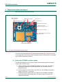
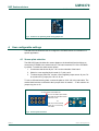
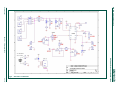
UM10370
User Manual for the PCF8883 Evaluation Kit OM11055
Rev. 02 — 2 December 2009
User manual
Document information
Info
Content
Keywords
Capacitive switch, sensor, proximity switch, PCF8883, OM11055,
PCF8883 evaluation board
Abstract
The OM11055 is a PCF8883 evaluation board which can be used to
demonstrate and evaluate the PCF8883 capacitive proximity switch. The
PCB is designed to make it easy to adjust the switch’s sensitivity. The
board can be powered using a Mini USB cable or a 9V battery.
UM10370
NXP Semiconductors
PCF8883 Evaluation Kit OM11055
Revision history
Rev
Date
Description
02
20091202
Fully updated version to reflect the change of the evaluation kit. Revision 1 was written for
the preliminary evaluation board which was marked “MA142_EVALBOARD.BRD”.
Revision 2 is valid for the new evaluation kit OM11055 (not marked as such on the board).
01
20090731
Initial release
Contact information
For additional information, please visit: http://www.nxp.com
For sales office addresses, please send an email to: [email protected]
UM10370_2
User manual
© NXP B.V. 2009. All rights reserved.
Rev. 02 — 2 December 2009
2 of 11
UM10370
NXP Semiconductors
PCF8883 Evaluation Kit OM11055
1. Introduction
This user manual describes the OM11055 evaluation kit. This board was developed in
order to provide a tool for application engineers and development engineers wishing to
try and evaluate the single channel PCF8883 capacitive proximity switch. A LED displays
the status of the switch; test points facilitate measurements of important signals.
The desired capacitive sensor area can vary in terms of material, form, size and
switching distance. Each particular switch configuration demands a suitable electrical
circuit for the input signal. This board allows to easily change the input circuit and the two
capacitors which define the sensitivity and reaction speed of the sensor in a typical
application. This offers the opportunity to rapidly evaluate many possible switching
configurations.
Features:
• Simple demonstration of the single channel PCF8883 capacitive proximity switch
• Jumper to select one of the three possible switch modes of the PCF8883
• Evaluate different sensor sizes (four different sensor plates included on the board) or
off board user defined sensors
• Two power supply options: via USB cable or a 9V battery
• Provisions for through-hole components allowing them to be easily changed
• Contents of the kit:
− One PCF8883 evaluation board
− One 3 ft USB A-B Mini Cable
• All documentation is available from the NXP website:
http://www.standardics.nxp.com/support/boards/pcf8883
2. Quick start
The OM11055 is an evaluation board for the single channel PCF8883 capacitive
proximity switch.
1. Apply power to the board by connecting the supplied mini USB cable to the PCF8883
board and the other end into a PC or a USB power adapter. Alternatively a 9V
battery can be used. The capacitive proximity sensor is now active.
2. With no jumpers on J9 (timed mode), touching the sense plate CP1 will turn on the
green output LED (LD1) for about two seconds.
Please read this manual completely for configuration options and modes.
UM10370_2
User manual
© NXP B.V. 2009. All rights reserved.
Rev. 02 — 2 December 2009
3 of 11
UM10370
NXP Semiconductors
PCF8883 Evaluation Kit OM11055
3. Board description and layout
Below the top view of the board is shown.
Option to connect an
external sense plate
Sensor output connections
Output LED, LD1
PCF8883
High impedance op-amp
Setting of output time
Mini USB connector for power
Setting of switch mode
(Push-button, toggle or pulse)
Connection for 9V battery
Optional header to select sense plate
(defaults to CP1)
Four sense plates (selected by J6)
Fig 1. Top view of the PCF8883 evaluation board
The lower halve is dominated by four sensor areas of different size. The actual circuit is
on the upper halve of the board. Arrows indicate the parts of interest which are described
more in detail in subsequent sections.
3.1 Setting the PCF8883 operation modes
The OM11055 allows the user to set one of three output switching behaviour modes,
using jumper J9. Refer to Fig 2:
a) With no jumper on J9, the PCF8883 will operate in pulse mode. The output is
activated for a defined time at each capacitive event. This defined time is
determined by C5.
b) With the jumper across the “TOG” and “TIM” pins, the PCF8883 will operate in
toggle mode (touch on, touch off).
c) With the jumper across the “SW” and “TIM” pins, the PCF8883 will operate in
momentary switch mode (push-button). The output is active as long as the
capacitive event lasts.
UM10370_2
User manual
© NXP B.V. 2009. All rights reserved.
Rev. 02 — 2 December 2009
4 of 11
UM10370
NXP Semiconductors
PCF8883 Evaluation Kit OM11055
Fig 2. Selection of operating mode using jumper J9
4. User configurable settings
The OM11055 kit allows the user to configure the PCF8883 sensor for evaluation in a
specific application.
4.1 Sensor plate selection
The OM11055 board includes four sensor plates on the board itself and provisions to
connect the PCF8883 to an external sensor. The board connects CP1 to the PCF8883
by default. To enable the other sensor options:
1. Cut the trace that shorts J6 pins 1 & 2 on the underside of the board.
2. Solder in a user supplied 8-pin header (0.1” pitch) at J6.
3. To select sensor plate CP4, connect a user-supplied jumper across J6, pins 7 &
8; to select CP3, jumper pins 5 & 6 of J6, etc.
To use an off board sensing plate, connect the plate at J14 & J18 using coax cable. The
coaxial shield must be connected to the input pin which is marked ‘−‘. In this case do not
jumper any pins on J6.
Cut trace under J6 to disable CP1
User can now add an 8pin header
and Jumper at J6 to select sensor
plates CP1 to CP4.
Or
User can connect external
sensor at J14 & J18 using
coax cable
Fig 3. Sensor plate selection
UM10370_2
User manual
© NXP B.V. 2009. All rights reserved.
Rev. 02 — 2 December 2009
5 of 11
UM10370
NXP Semiconductors
PCF8883 Evaluation Kit OM11055
The size and form of the sensor plate can be varied to obtain optimal switching behaviour
or to shape the sensor for a given application.
The following figure shows some creative examples of how the switch can be used with
sensors of various size and shape.
Fig 4. Examples of sensor areas and shapes
4.2 Sensitivity settings
The OM11055 board allows for easy modifications to the circuit to change the switch’s
sensitivity. It can be difficult to remove and install surface mount capacitors and resistors
without damaging the board. Therefore the OM11055 board includes holes to add
conventional through-hole passive components which enable quick evaluation of different
values. To remove the SMD components R1 and C1 from the circuit, cut the trace shorts
on the underside of the PCB at J4 and J5. Refer to the PCF8883 datasheet and the
application note AN10832 for details on adjusting the sensitivity.
Cut trace under J5 to disable C1
Cut trace under J4 to disable R1
Fig 5. Traces to be cut for sensitivity setting adjustment
UM10370_2
User manual
© NXP B.V. 2009. All rights reserved.
Rev. 02 — 2 December 2009
6 of 11
UM10370
NXP Semiconductors
PCF8883 Evaluation Kit OM11055
4.3 Power supply options
Power to the OM11055 PCB can be supplied using a mini USB cable (provided) or a 9V
battery. The 9V battery connector can be removed and a user provided power supply
could be connected at JP3 & JP4 for evaluation of a specific application. Using an
external power supply also allows for easy measuring of the power consumption.
Warning: There is no protection against reverse polarity of the external power supply.
4.4 High impedance op-amp
A high input impedance rail-to-rail input and output op-amp (U2) is included on the board
to measure the voltage at the CPC pin of the PCF8883. A capacitor is connected
between pin CPC and Vss. The value of this capacitor is used to adjust the sensitivity of
the switch. Since this is a very high impedance node, measuring directly with a probe
would disturb the control loop. Therefore this voltage buffer has been included on the
board. By default, this op-amp is not connected, as it would add to power consumption
measurements. To enable U2, install two pin headers and jumpers at J12 and J16.
Remark 1: Always first provide power to op-amp U2 (jumper J12) before connecting the
input to pin CPC of the PCF8883 (J16). Reversing this sequence could result in a CMOS
latch up.
Remark 2: The capacitor CCPC must be a good quality X7R type to minimize charge
leakage.
5. Sensor adjustment
It is recommended to start the evaluation of the application using the pre-assembled
components on the board since these have typical values and were tuned for use with
the default connected sensor plate CP1. This should give an adequate response in most
cases. In cases where the switch does not respond or responds unreliably, it is likely that
the input capacitance exceeds the specified input range. The voltage measured on CCPC,
via testpoint TP2, should ideally be approximately ½·VDDREG (note: ½·VDDREG which is half
the internally regulated supply voltage, not ½·VDD). The bias point can be optimized by
first changing CF (and possibly also RC) according to step 1 in the 5-step table below.
Once the switch works properly, further optimizations can be done by adjusting CCPC and
CLIN. Details concerning optimization of the biasing are given in application note
AN10832.
The circuit has three parameters that influence the switching behaviour. These are listed
below in order of their influence:
• Switch sensitivity, set by CCPC
• Calibration of the total capacitance on the sensor input using resistor RC and
capacitor CF
• Switching speed, set by CCLIN
UM10370_2
User manual
© NXP B.V. 2009. All rights reserved.
Rev. 02 — 2 December 2009
7 of 11
UM10370
NXP Semiconductors
PCF8883 Evaluation Kit OM11055
Table 1.
Optimizing step by step
Step
Component
Description
1
CIN (CF)
2
Min
Typ
Max
10 pF
CIN is the total input capacitance (CSensor + Ccable + CF). CF should
be chosen such that CIN is about 30 pF. This can be checked by
measuring the voltage over CCPC which should then be about ½ VDD.
30 pF
60 pF
RS
RS and CF form a low pass filter. The typical values are likely to be
correct for most applications.
-
6.8 kΩ
-
3
RC
This resistance compensates large input capacitances (long coaxial
cable, larger sensor plate area). Smaller resistor values should be
used with larger input capacitances.
5 kΩ
39 kΩ
50 kΩ
4
CCPC
CCPC determines the sensitivity of the sensor. If the sensitivity is
increased, the possibility of incorrect switching due to interfering
electrical fields is also increased. This parameter has a strong
influence on the switching characteristic.
90 nF
470 nF
2500 nF
5
CCLIN
CCLIN determines the internal sampling frequency and therefore the
reaction time of the switch. Smaller values of CCLIN correspond to
shorter reaction times. Shorter reaction times lead to increased
current consumption.
0 pF
22 pF
100 nF
6. Board schematic
On the next page the schematic of the Rev “A” OM11055 PCB is shown. Revision “A” is
identified by the fact that there is no revision number on the PCB. The schematic is also
available as a separate .PDF document on our website. Make sure to check our website
periodically for updates.
7. References and resource URLs
The documents below provide further useful information.
1. PCF8883 product datasheet.
2. AN10832; PCF8883 – capacitive proximity switch with auto-calibration.
Table 2.
Resource URLs
Item
Resource
Description and location
1
OM11055 eval kit
document package
Includes:
• This document
• Board schematic and BOM
• Links to datasheets and application notes
• Location:
http://www.standardics.nxp.com/support/boards/PCF8883
2
PCF8883 webpage Links to the datasheets and application notes
http://www.nxp.com/pip/PCF8883_1.html
UM10370_2
User manual
© NXP B.V. 2009. All rights reserved.
Rev. 02 — 2 December 2009
8 of 11
NXP Semiconductors
UM10370_2
User manual
Rev. 02 — 2 December 2009
UM10370
PCF8883 Evaluation Kit OM11055
9 of 11
© NXP B.V. 2009. All rights reserved.
Fig 6. Schematic of OM11055
UM10370
NXP Semiconductors
PCF8883 Evaluation Kit OM11055
8. Legal information
8.1 Definitions
Draft — The document is a draft version only. The content is still under
internal review and subject to formal approval, which may result in
modifications or additions. NXP Semiconductors does not give any
representations or warranties as to the accuracy or completeness of
information included herein and shall have no liability for the consequences
of use of such information.
to result in personal injury, death or severe property or environmental
damage. NXP Semiconductors accepts no liability for inclusion and/or use of
NXP Semiconductors products in such equipment or applications and
therefore such inclusion and/or use is for the customer’s own risk.
Applications — Applications that are described herein for any of these
products are for illustrative purposes only. NXP Semiconductors makes no
representation or warranty that such applications will be suitable for the
specified use without further testing or modification.
Export control — This document as well as the item(s) described herein
may be subject to export control regulations. Export might require a prior
authorization from national authorities.
8.2 Disclaimers
General — Information in this document is believed to be accurate and
reliable. However, NXP Semiconductors does not give any representations
or warranties, expressed or implied, as to the accuracy or completeness of
such information and shall have no liability for the consequences of use of
such information.
8.3 Trademarks
Notice: All referenced brands, product names, service names and
trademarks are property of their respective owners.
Right to make changes — NXP Semiconductors reserves the right to make
changes to information published in this document, including without
limitation specifications and product descriptions, at any time and without
notice. This document supersedes and replaces all information supplied prior
to the publication hereof.
Suitability for use — NXP Semiconductors products are not designed,
authorized or warranted to be suitable for use in medical, military, aircraft,
space or life support equipment, nor in applications where failure or
malfunction of a NXP Semiconductors product can reasonably be expected
UM10370_2
User manual
© NXP B.V. 2009. All rights reserved.
Rev. 02 — 2 December 2009
10 of 11
UM10370
NXP Semiconductors
PCF8883 Evaluation Kit OM11055
9. Contents
1.
2.
3.
3.1
4.
4.1
4.2
4.3
4.4
5.
6.
7.
8.
8.1
8.2
8.3
9.
Introduction .........................................................3
Quick start............................................................3
Board description and layout.............................4
Setting the PCF8883 operation modes ..............4
User configurable settings .................................5
Sensor plate selection ........................................5
Sensitivity settings..............................................6
Power supply options .........................................7
High impedance op-amp ....................................7
Sensor adjustment ..............................................7
Board schematic .................................................8
References and resource URLs .........................8
Legal information ..............................................10
Definitions ........................................................10
Disclaimers.......................................................10
Trademarks ......................................................10
Contents.............................................................11
Please be aware that important notices concerning this document and the product(s)
described herein, have been included in the section 'Legal information'.
© NXP B.V. 2009. All rights reserved.
For more information, please visit: http://www.nxp.com
For sales office addresses, email to: [email protected]
Date of release: 2 December 2009
Document identifier: UM10370_2
Mouser Electronics
Authorized Distributor
Click to View Pricing, Inventory, Delivery & Lifecycle Information:
NXP:
OM11055,598