1
To our customers,
Old Company Name in Catalogs and Other Documents
On April 1st, 2010, NEC Electronics Corporation merged with Renesas Technology
Corporation, and Renesas Electronics Corporation took over all the business of both
companies. Therefore, although the old company name remains in this document, it is a valid
Renesas Electronics document. We appreciate your understanding.
Renesas Electronics website: http://www.renesas.com
April 1st, 2010
Renesas Electronics Corporation
Issued by: Renesas Electronics Corporation (http://www.renesas.com)
Send any inquiries to http://www.renesas.com/inquiry.
Notice
1.
2.
3.
4.
5.
6.
7.
All information included in this document is current as of the date this document is issued. Such information, however, is
subject to change without any prior notice. Before purchasing or using any Renesas Electronics products listed herein, please
confirm the latest product information with a Renesas Electronics sales office. Also, please pay regular and careful attention to
additional and different information to be disclosed by Renesas Electronics such as that disclosed through our website.
Renesas Electronics does not assume any liability for infringement of patents, copyrights, or other intellectual property rights
of third parties by or arising from the use of Renesas Electronics products or technical information described in this document.
No license, express, implied or otherwise, is granted hereby under any patents, copyrights or other intellectual property rights
of Renesas Electronics or others.
You should not alter, modify, copy, or otherwise misappropriate any Renesas Electronics product, whether in whole or in part.
Descriptions of circuits, software and other related information in this document are provided only to illustrate the operation of
semiconductor products and application examples. You are fully responsible for the incorporation of these circuits, software,
and information in the design of your equipment. Renesas Electronics assumes no responsibility for any losses incurred by
you or third parties arising from the use of these circuits, software, or information.
When exporting the products or technology described in this document, you should comply with the applicable export control
laws and regulations and follow the procedures required by such laws and regulations. You should not use Renesas
Electronics products or the technology described in this document for any purpose relating to military applications or use by
the military, including but not limited to the development of weapons of mass destruction. Renesas Electronics products and
technology may not be used for or incorporated into any products or systems whose manufacture, use, or sale is prohibited
under any applicable domestic or foreign laws or regulations.
Renesas Electronics has used reasonable care in preparing the information included in this document, but Renesas Electronics
does not warrant that such information is error free. Renesas Electronics assumes no liability whatsoever for any damages
incurred by you resulting from errors in or omissions from the information included herein.
Renesas Electronics products are classified according to the following three quality grades: “Standard”, “High Quality”, and
“Specific”. The recommended applications for each Renesas Electronics product depends on the product’s quality grade, as
indicated below. You must check the quality grade of each Renesas Electronics product before using it in a particular
application. You may not use any Renesas Electronics product for any application categorized as “Specific” without the prior
written consent of Renesas Electronics. Further, you may not use any Renesas Electronics product for any application for
which it is not intended without the prior written consent of Renesas Electronics. Renesas Electronics shall not be in any way
liable for any damages or losses incurred by you or third parties arising from the use of any Renesas Electronics product for an
application categorized as “Specific” or for which the product is not intended where you have failed to obtain the prior written
consent of Renesas Electronics. The quality grade of each Renesas Electronics product is “Standard” unless otherwise
expressly specified in a Renesas Electronics data sheets or data books, etc.
“Standard”:
8.
9.
10.
11.
12.
Computers; office equipment; communications equipment; test and measurement equipment; audio and visual
equipment; home electronic appliances; machine tools; personal electronic equipment; and industrial robots.
“High Quality”: Transportation equipment (automobiles, trains, ships, etc.); traffic control systems; anti-disaster systems; anticrime systems; safety equipment; and medical equipment not specifically designed for life support.
“Specific”:
Aircraft; aerospace equipment; submersible repeaters; nuclear reactor control systems; medical equipment or
systems for life support (e.g. artificial life support devices or systems), surgical implantations, or healthcare
intervention (e.g. excision, etc.), and any other applications or purposes that pose a direct threat to human life.
You should use the Renesas Electronics products described in this document within the range specified by Renesas Electronics,
especially with respect to the maximum rating, operating supply voltage range, movement power voltage range, heat radiation
characteristics, installation and other product characteristics. Renesas Electronics shall have no liability for malfunctions or
damages arising out of the use of Renesas Electronics products beyond such specified ranges.
Although Renesas Electronics endeavors to improve the quality and reliability of its products, semiconductor products have
specific characteristics such as the occurrence of failure at a certain rate and malfunctions under certain use conditions. Further,
Renesas Electronics products are not subject to radiation resistance design. Please be sure to implement safety measures to
guard them against the possibility of physical injury, and injury or damage caused by fire in the event of the failure of a
Renesas Electronics product, such as safety design for hardware and software including but not limited to redundancy, fire
control and malfunction prevention, appropriate treatment for aging degradation or any other appropriate measures. Because
the evaluation of microcomputer software alone is very difficult, please evaluate the safety of the final products or system
manufactured by you.
Please contact a Renesas Electronics sales office for details as to environmental matters such as the environmental
compatibility of each Renesas Electronics product. Please use Renesas Electronics products in compliance with all applicable
laws and regulations that regulate the inclusion or use of controlled substances, including without limitation, the EU RoHS
Directive. Renesas Electronics assumes no liability for damages or losses occurring as a result of your noncompliance with
applicable laws and regulations.
This document may not be reproduced or duplicated, in any form, in whole or in part, without prior written consent of Renesas
Electronics.
Please contact a Renesas Electronics sales office if you have any questions regarding the information contained in this
document or Renesas Electronics products, or if you have any other inquiries.
(Note 1) “Renesas Electronics” as used in this document means Renesas Electronics Corporation and also includes its majorityowned subsidiaries.
(Note 2) “Renesas Electronics product(s)” means any product developed or manufactured by or for Renesas Electronics.
32
LCEVB-SH1
For SH1 Series Low-Cost Evaluation Board
Microcomputer Development Environment System
2003.4
www.rss.renesas.com
Microcomputer Development Environment System
LCEVB-SH1
SH1 Evaluation Board
User’s Manual
www.rss.renesas.com
LCEVB-SH1 – SH1-Series Low-cost Evaluation Board
User’s Manual
Published by
: Renesas System Solutions Asia Pte. Ltd.
Date
: April 1st, 2003, Version 1.0
Copyright (c) Renesas System Solutions Asia Pte. Ltd. All rights reserved
Trademarks
(a) General
All brands or product names in this manual are trademarks or registered trademarks of their respective companies or
organisation.
(b) Specific
Microsoft MS-DOS is registered trademark.
MS-Windows is a trademark of Microsoft Corporation.
Pentium is a registered trademark of Intel.
www.rss.renesas.com
IMPORTANT INFORMATION
•
READ this user’s manual before using this product.
•
KEEP the user’s manual handy for future reference.
Do not attempt to use this product until you fully understand its mechanism.
LCEVB-SH1 Evaluation Board:
Throughout this document, the term “LCEVB-SH1” shall be defined as the LCEVB-SH1 emulation system
produced only by Renesas System Solutions Asia Pte. Ltd. excluding all subsidiary products.
Purpose of LCEVB-SH1:
This emulation product is a software and hardware development tool for application systems employing the SH1
series microcomputer. It should only be used for the above purpose.
Improvement Policy:
Renesas System Solutions Asia Pte. Ltd. (hereafter collectively referred to as Renesas) pursues a policy of
continuing improvement in design, performance, and safety of the emulation products. Renesas reserves the right
to change, wholly or partially, the specifications, design, user’s manual, and other documentation at any time
without notice.
Target User of the Emulation Product:
User of this emulation product should have carefully read and thoroughly understood the information and
restrictions contained in the user’s manual before using it. Do not attempt to use the emulation product until you
fully understand its mechanism.
It is highly recommended that users who know how to operate this emulation product give proper training to users
who are not familiar with the operation of this product.
www.rss.renesas.com
LIMITED WARRANTY
Renesas warrants its emulator products to be manufactured in accordance with
published specifications and free from defects in material and/or workmanship.
Renesas, at its option, will repair or replace any emulator products returned intact to
the factory, transportation charges prepaid, which Renesas, upon inspection, shall
determine to be defective in material and/or workmanship. The foregoing shall
constitute the sole remedy for any breach of Renesas warranty. See the Renesas
warranty booklet for details on the warranty period. This warranty extends only to
you, the original Purchaser. It is not transferable to anyone who subsequently
purchases the emulator product from you. Renesas is not liable for any claim made
by a third party or made by you for a third party.
DISCLAIMER
RENESAS MAKES NO WARRANTIES, EITHER EXPRESS OR IMPLED,
ORAL OR WRITTEN, EXCEPT AS PROVIDED HEREIN, INCLUDING
WITHOUT
LIMITATION
THEREOF,
WARRANTIES
AS
TO
MARKETABILITY,
MECRCHANTABILITY,
FITNESS
FOR
ANY
PARTICULAR PURPOSE OR USE, OR AGAINST INFRINGEMENT OF ANY
PATENT. IN NO EVENT SHALL RENESAS BE LIABLE FOR ANY DIRECT,
INCIDENTAL OR CONSEQUENTIAL DAMAGES OF ANY NATURE, OR
LOSSES OR EXPENSES RESULTING FROM ANY DEFECTIVE EMULATOR
PRODUCT, THE USE OF ANY EMULATOR PRODUCT OR ITS
DOCUMENTATION, EVEN IF ADVISED OF THE POSSIBILITY OF SUCH
DAMAGES. EXCEPT AS EXPRESSLY STATED OTHERWISE IN THIS
WARRANTY. THIS EMULATOR PRODUCT IS SOLD “AS IS”. AND YOU
MUST ASSUME ALL RISK FOR THE USE AND RESULTS OBTAINED FROM
THE EMULATOR PRODUCT.
www.rss.renesas.com
State Law:
Some states do not allow the exclusion or limitation of implied warranty or liability for incidental or consequential
damages, so the above limitation or exclusion may not apply to you. This warranty gives you specific legal rights,
and you may have other rights which may varies from state to state.
The Warranty is Void in the Following Cases:
Renesas shall have no liability or legal responsibility for any problems caused by misuse, abuse, misapplication,
neglect, improper handling, installation, repair or modifications of the emulator product without Renesas’s prior
written consent or any problems caused by the user system.
Restrictions:
1. Earthing (applies only to manual for Renesas hardware products)
This hardware is designed for use with equipment that is fully earthed.
Ensure that all equipments used are appropriately earthed.
Failure to do so could lead to danger for the operator or damaged to equipments.
2. Electrostatic Discharge Precautions (applies only to manuals for Renesas hardware products)
This hardware contains devices that are sensitive to electrostatic discharge.
Ensure appropriate precautions are observed during handling and accessing connections.
Failure to do so could result in damage to the equipment.
All Right Reserved:
This user’s manual and emulator product are copyrighted and all rights are reserved by Renesas. No part of this
user’s manual, all or part, any be reproduced or duplicated in any form, in hardcopy or machine-readable form, by
any means available without Renesas‘s prior written consent.
Other Important Things to Keep in Mind:
1. Circuitry and other examples described herein are meant merely to indicate the characteristics and
performance of Renesas Technology‘s semiconductor products. Renesas assumes no responsibility for any
intellectual property claims or other problems that may result from applications based on the examples
described herein.
2. No license is granted by implication or otherwise under any patents or other rights of any third party or
Renesas.
3. MEDICAL APPLICATIONS: Renesas Technology’s products are not authorized for use in MEDICAL
APPLICATIONS without the written consent of the appropriate officer of Renesas Technology (Asia Sales
company). Such use includes, but is not limited to, use in life support systems. Buyers of Renesas
Technology’s products are requested to notify the relevant Renesas Technology (Asia Sales offices) when
planning to use the products in MEDICAL APPLICATIONS.
Figures:
Some figures in this user’s manual may show items different from your actual system.
Limited Anticipation of Danger:
Renesas cannot anticipate every possible circumstance that might involve a potential hazard. The warnings in this
user’s manual and on the emulator product are therefore not all inclusive. Therefore, you must use the emulator
product safely at your own risk.
www.rss.renesas.com
PREFACE
This guide explains how to setup and use the LCEVB-SH1 emulation system for the SH1 series of MCU.
Section 1
Introduction
Introduction of LCEVB-SH1 system including its package, specification and functions.
Section 2
Functional Description
Explain the functional blocks in LCEVB-SH1
Section 3
Board Options
Configurable components in LCEVB-SH1
Section 4
Hardware Startup
The necessary hardware installation to startup LCEVB-SH1
Section 5
Software Startup
The software installation sequences
Section 6
LCEVB-SH1 System Check
General check/diagnostic possible on LCEVB-SH1
Section 7
Tutorial Session
Provides a step by step guide in using the LCEVB-SH1 to perform emulation.
Section 8
Troubleshooting
Advises on some basic fault locating methods and commonly make mistakes.
Related Manuals:
• SuperH RISC engine C/C++ Compiler, Assembler, Optimizing, Linkage Editor User’s Manual
• SH7034, SH7032 Hardware Manual
• SH7020, SH7021 Hardware Manual
Table of Contents
SECTION 1. INTRODUCTION ............................................................................................................................ 1
1.1 OVERVIEW ....................................................................................................................................................................... 1
1.2 PACKAGE ......................................................................................................................................................................... 3
1.2.1
Software Components ............................................................................................................................................ 3
1.2.2
Hardware Components .......................................................................................................................................... 3
1.3 SPECIFICATIONS ............................................................................................................................................................... 4
1.4 SUMMARY OF LCEVB-SH1 FUNCTIONS.......................................................................................................................... 5
SECTION 2. FUNCTIONAL DESCRIPTION .................................................................................................... 6
2.1 SH1 RISC MICROCONTROLLER ....................................................................................................................................... 6
2.2 CLOCK CIRCUITRY ........................................................................................................................................................... 6
2.3 RESET CIRCUITRY ............................................................................................................................................................ 7
2.3.1
Reset Generator ..................................................................................................................................................... 7
2.3.2
Reset and Non-Maskable Interrupt (NMI) ............................................................................................................. 8
2.4 NMI CIRCUITRY .............................................................................................................................................................. 8
2.5 EPROM/ROM................................................................................................................................................................. 9
2.6 RAM................................................................................................................................................................................ 9
2.7 SERIAL INTERFACE ......................................................................................................................................................... 10
2.8 LED DRIVER .................................................................................................................................................................. 10
2.9 EXTERNAL USER INTERFACE ......................................................................................................................................... 10
SECTION 3. BOARD OPTIONS......................................................................................................................... 12
3.1 JUMPERS ........................................................................................................................................................................ 12
3.1.1
Jumper J1 and J2 (Crystal Clock Source) ........................................................................................................... 13
3.1.2
Jumpers J3, J4, and J5 (Analog Reference and Supply) ...................................................................................... 13
3.1.3
Jumper J6 (NMI).................................................................................................................................................. 13
3.1.4
Jumpers J7, J8, and J9 (Setting Operating Mode)............................................................................................... 13
3.1.5
Jumper J10 (LED Indicator Source).................................................................................................................... 14
3.1.6
Jumper J11 (DC Regulator Bypass) .................................................................................................................... 14
3.1.7
Jumpers J15, J16, J17, and J18 (Serial Port Disconnects) ................................................................................. 14
3.2 SERIAL PORT HARD-WIRING OPTIONS............................................................................................................................ 15
SECTION 4. HARDWARE STARTUP............................................................................................................... 18
4.1 INSTALLING THE LCEVB-SH1 BOARD .......................................................................................................................... 18
4.2 SERIAL COMMUNICATION CONNECTION ........................................................................................................................ 18
4.3 POWER SUPPLY CONNECTION ........................................................................................................................................ 18
4.3.1
Direct Power Supply ............................................................................................................................................ 19
4.3.2
Power-jet Power Supply ...................................................................................................................................... 19
SECTION 5. SOFTWARE STARTUP................................................................................................................. 20
5.1
5.2
5.3
HOST PC COMPUTER REQUIREMENT ............................................................................................................................. 20
HDI INSTALLATION ....................................................................................................................................................... 20
EVALUATION COMPILER AND ASSEMBLER INSTALLATION ............................................................................................ 23
SECTION 6. LCEVB-SH1 SYSTEM CHECK .................................................................................................... 24
SECTION 7. TUTORIAL SESSION ................................................................................................................... 26
7.1 INTRODUCTION .............................................................................................................................................................. 26
7.1.1
Overview .............................................................................................................................................................. 26
7.1.2
Compiling/Assembling ......................................................................................................................................... 26
7.1.3
How the Tutorial Program Works ....................................................................................................................... 26
7.2 EXECUTE HDI ................................................................................................................................................................ 28
7.2.1
Selecting the Target Platform .............................................................................................................................. 29
7.3 SETUP THE DEBUGGING ENVIRONMENT ......................................................................................................................... 30
7.4 MEMORY MAPPING ........................................................................................................................................................ 31
7.5 USER TARGET PROGRAM DOWNLOADING ...................................................................................................................... 32
7.6 DISPLAYING USER TARGET PROGRAM CODE ................................................................................................................. 33
7.7 USING BREAKPOINT (PC BREAKPOINT) ......................................................................................................................... 34
7.7.1
Setting PC Breakpoint ......................................................................................................................................... 34
7.8 EXECUTING USER TARGET PROGRAM ............................................................................................................................ 34
7.9 EXAMINING REGISTERS .................................................................................................................................................. 35
7.10
REVIEWING PC BREAKPOINTS .................................................................................................................................. 37
7.11
USER MEMORY MONITORING.................................................................................................................................... 38
7.11.1 Viewing User Memory ......................................................................................................................................... 38
7.12
WATCH WINDOW ...................................................................................................................................................... 39
7.12
LOCAL VARIABLE WATCH ........................................................................................................................................ 41
7.13
STEPPING USER TARGET PROGRAM .......................................................................................................................... 41
7.13.1 Single Step ........................................................................................................................................................... 41
7.14
SAVE SESSION ........................................................................................................................................................... 42
7.14
WHAT NEXT? ............................................................................................................................................................ 42
SECTION 8: TROUBLESHOOTING................................................................................................................. 43
APPENDIX A: FREQUENTLY ASKED QUESTIONS ................................................................................... 44
APPENDIX B: ASSEMBLER COMMANDS ..................................................................................................... 46
B.1
LEGEND ..................................................................................................................................................................... 46
B.2
COMMANDS SORTED ALPHABETICALLY.................................................................................................................... 46
B.3
COMMANDS SORTED BY TYPE ................................................................................................................................... 47
B.3.1
Data Transfer....................................................................................................................................................... 47
B.3.2
Arithmetic Operations.......................................................................................................................................... 48
B.3.3
Logical ................................................................................................................................................................. 48
B.3.4
Shift/Rotate .......................................................................................................................................................... 48
B.3.5
Branches .............................................................................................................................................................. 48
B.3.6
System Control..................................................................................................................................................... 49
APPENDIX C: MINI-PROJECT .......................................................................................................................... 50
C.1
C.2
C.3
BILL OF MATERIAL .................................................................................................................................................... 50
OPERATION ............................................................................................................................................................... 50
SOFTWARE LISTING ................................................................................................................................................... 51
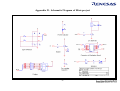
APPENDIX D: SCHEMATIC DIAGRAM OF MINI-PROJECT................................................................... 55
APPENDIX E: SCHEMATIC DIAGRAM OF LCEVB-SH1........................................................................... 56
RENESAS TECHNOLOGY (ASIA SALES OFFICES)
Section 1.
1.1
Introduction
Overview
The SH1 Evaluation Board (LCEVB-SH1) is an inexpensive demonstration / evaluation tool for the SH7000
family of RISC micro-controllers. It supports two members of the SH-1 family:
• SH7020 Series
: SH7021, SH7020
• SH7032 Series
: SH7034, SH7032
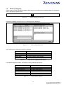
Figure 1.1 shows the physical layout of the LCEVB-SH1 system not drawn to scale.
J17
J18
Unregulated
Power
Supply
J11
J6
J2
J16
J15
HOST
SH7032
SRAM
OSC1
SRAM
J10
J8
EPROM
Figure 1-1
J1
J4
J9
J7
J5
J3
LCEVB-SH1 Layout
Schematic diagrams are provided at the back of this manual.
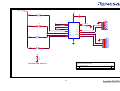
At the top level, the LCEVB-SH1 is composed of an SH processor, ROM, RAM, and two serial ports, as
shown in figure 1.2.
1
EPROM /
ROM
RAM
SH7032
Monitor
Port (to Host PC)
User
Port
Figure 1-2
LCEVB-SH1 Functional Block Diagram
The SH1 processor contains most of the decoding and glue logic necessary to implement an expanded
memory SH1-based system.
Read-only memory (ROM/EPROM) contains the Monitor Firmware. Two byte-wide (WORD) RAM blocks are
used side-by-side to provide word-wide reads and writes.
A serial transceiver supports two three-wire serial ports using the two on-board SH1 Universal Asynchronous
Receiver/Transmitters (UARTs). The respective usage of the ports are:
1 x Port is dedicated to the on-board Monitor Firmware for Host PC communication.
1 x Port is available to the user for user application system
The PC Host communication with LCEVB-SH1 is through PC interface program, HDI (Hitachi Debugging
Interface).
Users re-configuring LCEVB-SH1 I/O ports should be caution that pull-up resistors may be required for
proper operation in some the port configurations. In particular, users adding external memory in area 3
through 7 should be aware that the chip selects provided by SH1 are shared and may be floating until
properly configured.
2
1.2
Package
CD software
JJ
J
J
Serial Cable
Standard user Cable
J
JJ
J
J JJJ
JJ
LCEVB-SH1 User Manual
Packing list
Board spacer & nuts
Power cable
Figure 1-3
1.2.1
LCEVB-SH1 Package
Software Components
The software components included in the package are listed below.
• 1 x CD Software setup
- Setup.exe for HDI setup
- Adobe Reader Version 3.01
- SH Series Hardware manuals in pdf format
- SH Series Evaluation software and manuals in pdf format
Documents included in the package:
• 1 x User Manual
• 1 x Packing list
1.2.2
Hardware Components
The hardware components included in the package are listed below.
• 1 x LCEVB-SH1 System
• 4 x General User Cable
• 1 x Serial cable
• 1 x Power Supply Cable
• 5 x Board spacer & Nuts
3
1.3
Specifications
ITEM
MCU series
SPECIFICATION
•
SH7034, SH7032, SH7021, SH7022
Host PC
•
•
•
•
PC/AT i486 or above
Microsoft Windows 3.x / Window 95
One free serial port
Approximately 4 Mbytes of free hard disk space
Host-Interface
•
•
RS232C Serial Communication
Baud rate : 57600bps
Dimension
•
160 x 160 x 25 mm
Power supply
requirement
•
Power-jet (unregulated) Input
J11 set at 2-3 (input to regulator)
Or
Direct DC (regulated) Input
J11 set at 1-2 (bypass regulator)
•
Environmental
: 7.5 ~ 9 VDC (1A)
• Operating Temperature: 10oC to 35oC
• Humidity: 30% to 85% RH (no condensation)
• Corrosive Gas: None
Table 1-1
LCEVB-SH1 Specification
4
: 5 VDC (1A)
1.4
Summary of LCEVB-SH1 Functions
ITEM
Emulation
File
SPECIFICATION
• Performs close to real-time emulation of a target program
• High-level C debugging capability with SYSROF User Target
Program
• Performs simulated single step execution
• Supports MCU frequency : 20MHz
• Modifies and displays MCU registers
• Resets MCU
•
•
•
Memory
functions
•
Loads User Target Program (SYSROF or Motorola S-type
format)
Save target program in Motorola S-type format
Save Session
•
•
•
Fixed User usable Emulation Memory Address (H’0A000000 to
H’0A00FFFF)
Modifies and displays memory contents (including memory
mapped peripheral registers)
Dumps a range of memory contents
Fills data with specified pattern
Standard 64Kbyte high-speed RAM for emulation
Breakpoint
•
20 PC breakpoints
Single step
•
•
Performs simulated single step execution
Executes target program in step/s.
•
Table 1-2
LCEVB-SH1 Functions
5
Section 2.
Functional Description
The LCEVB-SH1 includes the following components:
•
•
•
•
•
•
•
•
•
SH1 (SH7032) RISC Microcomputer
Clock circuitry
Reset circuitry
NMI circuitry
ROM memory
RAM memory
Serial interface
LED driver
External user interface
Complete LCEVB-SH1 schematics are provided as part of the LCEVB-SH1 kit and are referenced throughout this
chapter.
2.1
SH1 RISC Microcomputer
Because the SH1 (SH7032) provides many on-board functions required to implement an expanded-memory microcontroller system (for example, address area decoding), the amount of glue logic required is minimized.
2.2
Clock Circuitry
The LCEVB-SH1 may use one of two clock sources:
• AT-cut parallel resonating system
• Oscillator
The SH1 is designed to operate with an AT-cut parallel resonating crystal (default clock source, Y1).
OSC1
3 2 1
2 1
J1
J2
In Use
Y1
Figure 2-1
Selecting AC-cut parallel resonating system for system clock
6
Alternatively by changing the jumpers setting of both J1 and J2, a standard TTL “can” oscillator may be used.
OSC1
3 2 1
2 1
In Use
J1
J2
Y1
Figure 2-2
Selecting Oscillator system for system clock
The setting of J1 and J2 can be shown below:
Jumper
setting
J1
J2
1-2 1-2
AT-cut parallel resonating system (Y1 & circuitry)
2-3
Oscillator (OSC1)
Assignment
(default)
NC
Table 2-3
2.3
Reset Circuitry
2.3.1
Reset Generator
Jumper J1 and J2 setting
The reset generator for the LCEVB-SH1 is a Dallas Semiconductor DS1233 “Econo Reset” device.
The DS1233 monitors its supply voltage. When the supply voltage is out of tolerance level, the DS1233 pulls its
reset input/output line active-low. This condition continues indefinitely. After the voltage reaches tolerance level
again, the reset is held low for an additional 350 ms to allow for final supply stabilization before release the
processor from reset state.
The DS1233 monitors its own reset output so that a pushbutton can be used as a reset source. The DS1233 debounces the input from the pushbutton (S1) provides a 350-ms reset signal when S1 is released.
Quickly switching power off then on supplying to the board may not allow VCC to fall low enough to generate a reset
pulse. In practice, the SH1 usually continues to operate normally. Rapid switching of the power supply stresses
the integrated circuit components and is not recommended.
7
2.3.2
Reset and Non-Maskable Interrupt (NMI)
The SH1 distinguishes between a power-on reset and a manual reset by sampling the state of the NMI input when
the RESET line goes high. If NMI is high at this point, a power-on reset sequence is initiated internally, and the
SH1 is initialised throughout. If NMI is low, the manual reset sequence initiates the SH1 except the following:
• bus state controller
• pin function controller
• I/O ports
The LCEVB-SH1 by default generates a power-on reset when:
• power is applied into the system
• reset pushbutton is depressed and released
2.4
NMI Circuitry
The NMI input of the SH1 is an independent edge-triggered input. NMI may be generated on the positive or
negative-going transition, depending on the setting of the Interrupt Control register (ICR) NMIE bit.
The LCEVB-SH1 uses two NAND gates (U3A and U3B) as an inverter to de-bounce the output of momentary
pushbutton S2. In the quiescent case, the output of U3B (and thus the SH1 NMI input) is high. Closing/depressing
S2 cause the NMI signal to go low until S2 is released. The default value of ICR.NMIE is 0, and NMI is generated
when NMI goes low. Multiple bounces of the switch on the normally open closure will have no further effect
(switches bounce on the active closure only), and the NMI signal will stay low until S2 is released.
Since the quiescent state of NMI is high, closing the reset pushbutton (S1) always generates a power-on reset. In
other words, when the board is reset, all SH1 internal circuitry is normally affected. It is possible to generate a
manual reset (leaving the bus state controller, pin function controller, and I/O port values untouched) with the
following sequence:
1. Close the reset switch (S1), putting the SH1 into reset state.
2. Close the NMI switch (S2), generating a negative-going edge on NMI, which is ignored.
3. Release the reset switch (S1), starting the SH with NMI low.
4. Release the NMI switch (S2), returning NMI to its base state.
Alternatively, external connections can be used to affect the NMI signal if jumper J6 is changed from its default
setting.
Jumper
setting
(J6)
1-2
2-3
Assignment
Internal usage
External usage (to S2)
Table 2-4
(default)
Jumper J6 setting
8
2.5
EPROM/ROM
The LCEVB-SH1’s EPROM/ROM memory is provided by U4, which is configured to contain 64k × 8, 27(C)512family device. Below shows the memory map.
H’ 00,000,000
64K x 8 EPROM/ROM
(27C512)
H’ 00,00F,FFF
H’ 0A,000,000
64K x 8 SRAM
(62256)
H’ 0A,00F,FFF
Figure 2-3
LCEVB-SH1 Memory Map
In either case, the EPROM/ROM is located in area 0 of the SH1 memory space, starting at location 0. U4 is always
accessed a byte at a time. The memory area select signal, CS0 is generated by the SH1 and is sufficient to select
either device.
The value of SH1 wait state control register 3 (WCR3) bits A02LW1 and A02LW0 control the number of wait states
automatically inserted for accesses to area 0 and area 2 by the SH1 on-board bus state controller. Since RAM
memory is located in area 2, the access time requirements for both RAM and EPROM/ROM must be considered
when setting WCR3 and set to conform with the slowest of the two (normally EPROM/ROM).
2.6
RAM
The LCEVB-SH1’s Emulation RAM is at U5 and U6, which contain a pair of 32k × 8, 62256-family static CMOS
RAM organized for word-wide access. Figure 3.3 shows the memory map.
In either case, the RAM memory is located in area 2 of the SH1 memory space, nominally starting at location
H'2000000. The configuration of U5 and U6 is 16 bits wide, so for proper access this RAM memory must be
accessed starting at address H'A000000. When RAM is referenced at this address, the memory area select signal
CS2, high byte strobe (HBS), and low byte strobe (LBS) signals are generated by the SH1 and are externally
combined by OR gates U7A and U7B before being used as the RAM device select signal. In order for HBS and
LBS signals to be generated, bit BAS of the SH1 bus control register (BCR) must be asserted.
The value of SH1 wait-state control register 3 (WCR3) bits A02LW1, A02LW0 controls the number of wait states
automatically inserted for accesses to area 0 and area 2 by the SH1 bus state controller. Since EPROM/ROM
memory is located in area 0, the access time requirements for both RAM and EPROM/ROM must be considered
when setting WCR3 and set to conform with the slowest of the two, normally ROM. Since a minimum of one waitstate is used for external accesses, and this corresponds to an access time of 120ns at a CPU speed of 20MHz, it
is likely to be most convenient to use 120ns RAM and EPROM/ROM.
9
2.7
Serial Interface
The LCEVB-SH1 supports two three-wire serial channels using the two identical SH1 SCI UART-type devices:
• SCI0
• SCI1
Of these, SCI1 is normally dedicated to use by Monitor Firmware for communication with a Host PC. SCI0 is
available for User Target System development.
U9 is a serial transceiver device that translates RS-232 signals to logic levels and vice-versa. This device provides
two channels in each direction, enough to support TxD and RxD for each of the two channels. U9 is a standard 16pin MAX-232 device.
2.8
LED Driver
U3 (7400, NAND chip), is used to drive LED D1 (Green LED). Jumper J10 should be set to 2-3 connecting to SH1
port pin PA15. Alternately, jumper J10 set to 1-2 cause connection to SH1 port pin PB15.
Jumper
setting
(J10)
1-2
Connecting to PB15
2-3
Connecting to PA15
Assignment
Table 2-5
2.9
(default)
Jumper J10 setting
External User Interface
The External User Interface output most of the Processor (SH1) signals to User Target System. The arrangement
is consistent keeping:
• Signal lines short
• Board design simple
• Signals are assigned compatible with Japan User Cable
• Lines potentially used for analog signals isolated
The external user interface consists of 4 two-row connectors of 50 pins each.
10
Connector*
Signals
UCN1
•
•
•
SH data lines (D0–D15)
SH Port B lines(PB14 & PB15)
SH address lines (A0-A5)
UCN2
•
•
•
SH address lines (A6–A21)
CS0-CS3
SH1 Port A lines (PA0-PA3)
•
•
•
•
SH Port A lines (PA4–PA15)
CK
WDTOVF
NMI
•
•
•
•
•
SH Port B lines (PB0-PB13)
SH Port C lines (PC0–PC7)
AVCC
AVREF
AVSS
UCN3
UCN4
Table 2-6
External User Interface pin-assignment
Note: Each of these external user interface connectors includes VCC, normally at +5 V.
Trivial external circuitry may use VCC from the LCEVB-SH1. External circuits drawing >50mA at +5V should
be powered by an independent power supply.
Note the positioning of pin 1 on each connector. The pins are numbered odd-even as shown below:
UCN1
UCN2
UCN3
UCN4
1
2
1
2
1
2
1
2
3
4
3
4
3
4
3
4
5
6
5
6
5
6
5
6
7
8
7
8
7
8
7
8
9
10
9
10
9
10
9
10
11
12
11
12
11
12
11
12
13
14
13
14
13
14
13
14
15
16
15
16
15
16
15
16
17
18
17
18
17
18
17
18
49
50
49
50
49
50
49
50
Figure 2-4
User External Interface Connector Configuration
11
Section 3.
Board Options
The LCEVB-SH1 provides a number of user-settable optional configurations. All of these are chosen by jumper
settings.
3.1
Jumpers
LCEVB-SH1 jumpers allow User to configure the board as required for evaluation. For simplicity, all jumpers are:
• three-pin header
or
• two-pin header
In each case, the default jumper setting is pin 1 to pin 2 (1-2). For most LCEVB-SH1 uses, these settings need not
be changed.
Jn
Use
Default (1-2)
Alternate (2-3)
J2
XTAL
Selection
Resonating
XTAL
No connection
J3
J4
J5
AVCC
AVREF
AVCC
= digital VCC
= digital VCC
= digital VSS
Set externally
Set externally
Set external
J6
NMI
Internal
External
J7
J8
J9
J10
SH MD2
SH MD1
SH MD0
User LED
Mode 0
Set according to table 4.2
PB15 drives LED
PA15 drives LED
J11
Power
Direct Power supply
Power-jet Power supply
(DC adapter)
J12
Power
Unregulated Power Supply (power-jet power supply)
JP1
Power
Regulated Power Supply (direct power supply)
TxD1
PB11 connected
J16
RxD1
PB10 connected
J17
TxD0
PB9 connected
J18
RxD0
PB8 connected
J1
TTL XTAL
Do not connect Jumper if
•
PB11
•
PB10
•
PB9
•
PB8
J15
Table 3-1
are to be left open.
Jumper Settings and Options
The following sections describe each jumper and its alternative settings.
12
3.1.1
Jumper J1 and J2 (Crystal Clock Source)
The LCEVB-SH1 comes with two types of clock source:
• AT-cut parallel resonant crystal
• TTL Can Crystal
Either clock source may be used. To make a selection, simply make the necessary connection on jumper J1 and
J2. The default crystal clock source is the AT-cut parallel resonant crystal with J1 (1-2) and J2 (1-2) connected. To
use the TTL can crystal simply change connection to J1 (2-3) and remove Jumper at J2 (1-2).
3.1.2
Jumpers J3, J4, and J5 (Analog Reference and Supply)
As described in section 14 of the SH7032 and SH7034 RISC Hardware Manual, the port C bits of the SH1 may be
configured as analog inputs. In this case, reference voltages for analog signals become important. The default
settings of these three jumpers route on-board digital references and the digital VCC to the SH1 analog subsystem.
For demonstration purposes, this configuration may be sufficient. However, to demonstrate the full capabilities of
the SH1 analog subsystem, as well as to reduce noise in the analog subsystem, it may be desirable to use external
sources for some or all of these signals.
The recommended noise suppression capacitors are provided on reference circuits as recommended by the
hardware manual section 14.7.2.
If an external analog VCC (AVCC) is provided to the SH1 on Header 4 Pin 1, set J3 (2-3).
If an external analog reference voltage (VREF) is provided to the SH on Header 4 Pin 2, set J3 (2-3).
If an external analog ground (AVSS) is provided to the SH on Header 4 Pin 12, set J5 (2-3).
Leaving any of these jumpers open is not recommended.
3.1.3
Jumper J6 (NMI)
Default (1-2) Setting
: The SH NMI input is controlled by the set-reset flip-flop de-bounce circuitry
implemented with AND gates U3A and U3B (schematic diagram).
Alternate (2-3) Setting
: The SH1 NMI input is controlled by an external signal (on-board pull-up is
provided).
Open Setting
: Not recommended. The SH1 NMI signal should be driven in most conditions.
Failure to do so may cause the board to operate erratically.
3.1.4
Jumpers J7, J8, and J9 (Setting Operating Mode)
As described in section 3 of the SH7032 and SH7034 RISC Hardware Manual, the operating mode of the SH1
processor is set at device initialization time by the settings of the three mode inputs, MD0, MD1, and MD2. These
settings should not be changed while the SH1 is running. Table 4.2 lists jumper settings for these modes.
Leaving any of these jumpers open is not recommended. Settings not shown in table 4.2 are currently undefined.
13
Mode J7
J8
J9
Description
Implementation
0
1
2
7
1-2
1-2
2-3
2-3
1-2
2-3
1-2
2-3
Memory area 0 is 8-bit
Memory area 0 is 16-bit
Memory area 0 is on-chip
EPROM programming
Default
Not supported
SH7034 only
Not supported
1-2
1-2
1-2
2-3
Table 3-2
3.1.5
Operating Mode Settings
Jumper J10 (LED Indicator Source)
LED D1 (Green LED) may be driven by SH1 port signal PA15 by setting J10 (2-3) or PB15 by setting J10 (1-2). The
default source is PB15. If these two sources is allocated for other use, remove the jumper at J10.
3.1.6
Jumper J11 (DC Regulator Bypass)
Jumper J11 selects the use of on-board DC Regulator. If Unregulated Power input is used through Connector J12,
Jumper J11 setting to 2-3 enables the regulator to regulate a usable voltage of 5VDC for LCEVB-SH1.
Either, if connector JP1 is used to used to provide direct power supply of regulated 5VDC to LCEVB-SH1, Jumper
J11 setting should be at 1-2 (bypass the on-board regulator).
3.1.6.1 Connector J12 (Power-jet Connector)
General power-jet connector allowing unregulated power (≥7.5V) to be supplied to LCEVB-SH1. Note that if this
type of power supply is selected over the direct power supply (regulated) to JP1, J11 should be set to 2-3
3.1.6.2 Connector JP1 (Direct Power Connector)
Direct regulated Power supplying 5VDC to LCEVB-SH1. Note that J11 should be set to 1-2
3.1.7
Jumpers J15, J16, J17, and J18 (Serial Port Disconnects)
UART1 is dedicated by default to the Firmware Monitor. UART0 is unassigned, and usable by User Target
System. The port pins (TxD0, RxD0 and TxD1, and RxD1) associated with transmitting and receiving data for both
UARTs are connected to a serial transceiver device.
In some applications it may be necessary to use some or all of these pins for another purpose, in which case the
connections of these port pins to the transceiver device should normally be disconnected.
These jumpers may be left open because the logic inputs of the MAX232 transceivers are internally pulled up
weakly to VCC. Alternate devices may not include these pull-ups.
To free PB8, remove Jumper at J18 (1-2). To free PB9, remove Jumper at J17 (1-2).
To free PB10, remove Jumper at J16 (1-2). To free PB11, remove Jumper at J15 (1-2). This will normally disable
serial communications between the LCEVB-SH1 and its host.
14
3.2
Serial Port Hard-wiring Options
As supplied, the LCEVB-SH1 supports three-wire serial communication. No direct provision is made for additional
handshaking signals that may be required by host computers or terminals in some configurations. It is not possible
to support all configurations, but there is provision for Jumpers providing some additional signals. Active hardware
control is not possible without additional hardware.
15
UCN1
Pin
No.
1
3
5
7
9
11
13
15
17
19
21
23
25
27
29
31
33
35
37
39
41
43
45
47
49
Signal
Name
PB14
GND
GND
GND
GND
GND
GND
GND
GND
GND
GND
GND
GND
GND
GND
GND
GND
GND
GND
GND
GND
GND
GND
GND
GND
Pin
No.
2
4
6
8
10
12
14
16
18
20
22
24
26
28
30
32
34
36
38
40
42
44
46
48
50
Signal
Name
PB15
GND
AD0
AD1
AD2
AD3
AD4
AD5
AD6
AD7
AD8
AD9
VCC
AD10
AD11
AD12
AD13
AD14
AD15
A0
A1
A2
A3
A4
A5
UCN3
Pin
No.
1
3
5
7
9
11
13
15
17
19
21
23
25
27
29
31
33
35
37
39
41
43
45
47
49
Signal
Name
GND
GND
GND
GND
GND
GND
GND
GND
GND
GND
GND
GND
GND
GND
GND
GND
VCC
UNMI
GND
GND
GND
GND
GND
GND
GND
Pin
No.
2
4
6
8
10
12
14
16
18
20
22
24
26
28
30
32
34
36
38
40
42
44
46
48
50
Signal
Name
PA4
PA5
PA6
PA7
GND
PA8
PA9
PA10
PA11
PA12
PA13
PA14
PA15
VCC
CK
VCC
WDTOVF
-
UCN2
Pin
No.
1
3
5
7
9
11
13
15
17
19
21
23
25
27
29
31
33
35
37
39
41
43
45
47
49
Signal
Name
GND
GND
GND
GND
GND
GND
GND
GND
GND
GND
GND
GND
GND
VCC
GND
GND
GND
GND
GND
GND
GND
GND
GND
GND
GND
Pin
No.
2
4
6
8
10
12
14
16
18
20
22
24
26
28
30
32
34
36
38
40
42
44
46
48
50
Signal
Name
A6
A7
A8
A9
A10
A11
A12
A13
A14
A15
GND
A16
A17
A18
A19
A20
A21
CS0
CS1
CS2
CS3
PA0
PA1
PA2
PA3
UCN4
Pin
No.
1
3
5
7
9
11
13
15
17
19
21
23
25
27
29
31
33
35
37
39
41
43
45
47
49
Signal
Name
No ADC
GND
GND
GND
GND
GND
GND
GND
GND
GND
GND
GND
VCC
GND
GND
GND
GND
GND
GND
GND
GND
GND
GND
GND
GND
Pin
No.
2
4
6
8
10
12
14
16
18
20
22
24
26
28
30
32
34
36
38
40
42
44
46
48
50
Signal
Name
No ADC
No ADC
No ADC
No ADC
No ADC
No ADC
No ADC
No ADC
No ADC
No ADC
PB0
PB1
PB2
PB3
PB4
PB5
PB6
PB7
GND
PB8
PB9
PB10
PB11
PB12
PB13
Table 2-7
SH7020/21 Connector Pinout
16
UCN1
Pin
No.
1
3
5
7
9
11
13
15
17
19
21
23
25
27
29
31
33
35
37
39
41
43
45
47
49
Signal
Name
PB14
GND
GND
GND
GND
GND
GND
GND
GND
GND
GND
GND
GND
GND
GND
GND
GND
GND
GND
GND
GND
GND
GND
GND
GND
Pin
No.
2
4
6
8
10
12
14
16
18
20
22
24
26
28
30
32
34
36
38
40
42
44
46
48
50
Signal
Name
PB15
GND
AD0
AD1
AD2
AD3
AD4
AD5
AD6
AD7
AD8
AD9
VCC
AD10
AD11
AD12
AD13
AD14
AD15
A0
A1
A2
A3
A4
A5
UCN3
Pin
No.
1
3
5
7
9
11
13
15
17
19
21
23
25
27
29
31
33
35
37
39
41
43
45
47
49
Signal
Name
GND
GND
GND
GND
GND
GND
GND
GND
GND
GND
GND
GND
GND
GND
GND
GND
VCC
UNMI
GND
GND
GND
GND
GND
GND
GND
Pin
No.
2
4
6
8
10
12
14
16
18
20
22
24
26
28
30
32
34
36
38
40
42
44
46
48
50
Signal
Name
PA4
PA5
PA6
PA7
GND
PA8
PA9
PA10
PA11
PA12
PA13
PA14
PA15
VCC
CK
VCC
WDTOVF
-
UCN2
Pin
No.
1
3
5
7
9
11
13
15
17
19
21
23
25
27
29
31
33
35
37
39
41
43
45
47
49
Signal
Name
GND
GND
GND
GND
GND
GND
GND
GND
GND
GND
GND
GND
GND
VCC
GND
GND
GND
GND
GND
GND
GND
GND
GND
GND
GND
Pin
No.
2
4
6
8
10
12
14
16
18
20
22
24
26
28
30
32
34
36
38
40
42
44
46
48
50
Signal
Name
A6
A7
A8
A9
A10
A11
A12
A13
A14
A15
GND
A16
A17
A18
A19
A20
A21
CS0
CS1
CS2
CS3
PA0
PA1
PA2
PA3
UCN4
Pin
No.
1
3
5
7
9
11
13
15
17
19
21
23
25
27
29
31
33
35
37
39
41
43
45
47
49
Signal
Name
AVCC
GND
GND
GND
GND
GND
GND
GND
GND
GND
GND
GND
VCC
GND
GND
GND
GND
GND
GND
GND
GND
GND
GND
GND
GND
Pin
No.
2
4
6
8
10
12
14
16
18
20
22
24
26
28
30
32
34
36
38
40
42
44
46
48
50
Signal
Name
AVREF
PC0
PC1
PC2
PC3
AVSS
PC4
PC5
PC6
PC7
PB0
PB1
PB2
PB3
PB4
PB5
PB6
PB7
GND
PB8
PB9
PB10
PB11
PB12
PB13
Table 2-7
SH7032/34 Connector Pinout
17
Section 4.
4.1
Hardware Startup
Installing the LCEVB-SH1 Board
Installing the LCEVB-SH1 requires connecting the following:
• Serial communication cable to Host PC
• Power supply
4.2
Serial Communication Connection
Plug-in the Serial Communication Cable provided to LCEVB-SH1 and the Host PC Serial Communication Port
(usually at the rear of the PC). LCEVB-SH1 System support the following Ports:
• COM1
• COM2
• COM3
• COM4
LCEVB-SH1 System will auto-detect the correct Port connection at HDI (Interface software) startup.
Ensure that Host PC is off when you are making the connection.
4.3
Power Supply Connection
Two type of Power supplies can be used on LCEVB-SH1, they are:
• Direct Power Supply
• Power-jet Power Supply
To select between Direct Power Supply or Power-jet Power Supply simply change the connection at Jumper J11.
Jumper J11 (1-2) is the default setting at shipment (using direct power supply of 5VDC). The connection should
not be left open.
Jumper
setting
(J11)
Assignment
1-2
Direct power supply of 5VDC, regulated
(default)
2-3
Power-jet power supply of ≥7.5VDC,
unregulated
Table 4-1
Jumper J11 setting
18
4.3.1 Direct Power Supply
The LCEVB-SH1 hardware uses a direct power supply of 5VDC (≈100mA) injecting into JP1 with J11 jumper set to
1-2 (bypass regulator).
5
Regulated
Power supply
5VDC
JP1
1
3
1
J11
J12
Figure 4-2
Direct Power supply to LCEVB-SH1
The pin assignment of JP1:
Pin
Assignment
1
2
3
4
5
+5VDC
NC
NC
NC
0V (GND)
Table 4-2
4.3.2
Pin assignment of JP1
Power-jet Power Supply
Alternatively, a power-jet supplying unregulated voltage (≥7.5VDC) to LCEVB-SH1 through J12. The power-jet
configuration:
-VDC
Figure 4-2
+VDC
Power-jet configuration for LCEVB-SH1
The power-jet connection with the appropriate J11 setting of the jumper at 2-3 (using regulator):
5
JP1
1
3
1
J11
Unregulated
Power supply
≥7.5VDC
J12
Figure 4-3
Power-jet Power supply for LCEVB-SH1
Since total power consumption can vary widely due to external connections, SH1 port state, and memory
configuration, generally use a power supply capable of providing at least 500mA at +5VDC (regulated) ±5%.
19
Section 5.
5.1
Software Startup
Host PC Computer Requirement
HDI is powerful yet easy to use MS-Window based Interface Program communicating with LCEVB-SH1 hardware
system. For program development with the LCEVB-SH1 package, you will need a PC:
• Capable of hosting the Renesas’s tools, editing files, and communicating with the evaluation board. The
computer must be an i386 ,i486 or Pentium standard PC running DOS 5.0 or higher with Windows 3.x or
higher
• Memory of at least 8Mbytes is highly recommended
• CD-ROM drive is required since the supplementary tools and tutorials are distributed on CD-ROM
• Standard serial port must be available on host computer for communication with the LCEVB-SH1 system
• Harddisk is required (at least 6Mbyte of free space). The supplementary tools and tutorials files require a trivial
amount of hard disk space
• Text editor capable of editing program source files without inserting non-printing characters in the file. An ASCII
editor such as EDIT is acceptable.
• SuperH RISC engine C/C++ Compiler, Assembler, Optimizing Linkage Editor.
• Evaluation copy of these tools is available in the distribution CD-ROM.
5.2
HDI Installation
Install the HDI software from the CD-ROM is as follows:
• Startup Windows if it is not already running.
• Close all other applications that are running.
• Insert Installation CD-ROM into CD-ROM Drive
• Click (or Double-click) on the CD-ROM Drive to view the content of the CD-ROM
• Click (or Double-click) on the folder HDI16 to view its content
• Execute LSH1_101.EXE by clicking (or Double-clicking).
The following Welcome! Screen will be displayed:
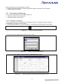
Figure 5-1
Welcome Screen of HDI for LCEVB-SH1
20
• Click Next to proceed with the installation.
• Read the update information for any important information concerning the installation
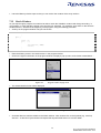
Figure 5-2
Latest information on HDI for LCEVB-SH1
• Click Next to proceed
• Select which directory you wish to install HDI for LCEVB-SH1
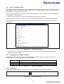
Figure 5-3
Selecting which Directory to install HDI for LCEVB-SH1
• Click Browse if you wish to change the default directory. The default directory is C:\Program File\Hitachi
Debugging Interface 16, or specify an alternative directory and click OK.
• Click Next to proceed
21
Figure 5-4
Selecting which Group the HDI application should place its Icon
• The Program Group is where icons for HDI application will be. The default Program Group (ProgMan Group) is
Hitachi Debugging Interface 16.
• Click Next to proceed
• Click Next in the Ready to Install Dialog-box to start installation
The installation will then copies the necessary HDI for LCEVB-SH1 files into the specified directory:
Figure 5-5
Installation Progress
Finally icons for HDI will be created into the Program Group specified earlier. The installer creates the following
icons in the program group (Start Menu\Programs) you specified, by default HDI:
Figure 5-6
HDI Icons
22
These icons have the following functions:
• Hitachi Debugging Interface
• Uninstall Hitachi Debugging Interface
5.3
: HDI for LCEVB-SH1
: will remove HDI for LCEVB-SH1, and its associated
files, if you need to uninstall it at any stage
Evaluation Compiler and Assembler Installation
Compiling/Assembling of SH Series Embedded codes need the following tools:
Evaluation SuperH RISC engine C/C++ Compiler, Assembler, Optimizing Linkage Edition
Install these tools by executing SETUP.EXE in EVAL directory. A similar automated installation process will copy
all the necessary files and setup the environment variables.
Note that User need to restart Host PC to complete this stage of installation.
23
Section 6.
LCEVB-SH1 System Check
The next step is to run the HDI software to check that the LCEVB-SH1 System is working correctly. Follow the
sequence below (ensure both the Serial Cable and Power Supply is properly connected up to LCEVB-SH1 before
continuing):
• Switch on the LCEVB-SH1 and check that the red LED is illuminated.
• Select Hitachi Debugging Interface under the Start Menu/Programs/Hitachi Debugging Interface menu or
Double-click the HDI icon:
Figure 6-1
HDI Application Icon
When everything is setup correctly the status bar will display Link up to indicate that everything is set up correctly,
and the HDI screen will be displayed as shown below:
Figure 6-2
HDI startup Desktop
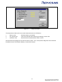
Perform the Diagnostic test by selecting View/Diagnostic Window… to verify the LCEVB-SH1 functionality:
24
Figure 6-3
Diagnostic Window
The test performed above will cover certain features/functions of LCEVB-SH1:
1.
2.
3.
Memory Test
Port_B LED Test
Checksum Test
: Emulation Memory accessible
: Inter-active test with User observing the blinking of Green LED
: Ensure that the Firmware Monitor used is correct
Note that performing Diagnostic will cause the HDI to restart. Thus, never perform Diagnostic Test in-between
Emulation process, as Emulation Memory content will be erased.
25
Section 7.
7.1
Tutorial Session
Introduction
The following describes a sample debugging session, designed to introduce the main features of the LCEVB-SH1
Evaluation Board used in conjunction with the Hitachi debugging interface (HDI) software.
The tutorial is designed to run on the Emulation memory so that it can be used without connecting the LCEVB-SH1
to an external user system.
The tutorial is based on a simple C program.
Before reading this chapter:
• Setup the LCEVB-SH1 and verify that it is communicating correctly with HDI.
• Make sure you are familiar with the architecture and instruction set of SH1 before continuing. For more
information refer to
• SH1/SH2 Series Programming Manual
• SH7034 or SH7021 Series Hardware Manual
7.1.1
Overview
This Tutorial program is an infinite loop that sort elements based on NAME in the alphabetical order, and AGE and
ID in the ascending order. It is a simple C program to illustrate the capabilities of LCEVB-SH1 with simple C code.
7.1.2 Compiling/Assembling
The Tutorial is provided on the installation disk as the file tutorial.c. A workable version of the Tutorial should be
compiled at User Host PC by executing Tutorial.bat, this needs the Evaluation SuperH RISC engine C/C++
Compiler, Assembler, Optimizing Linkage Edition (refer to section 5.3).
Note that the following files need customization:
• Tutorial.bat
• Tutorial.sub
Depending on the directory path where the Compiling/Assembling Tools are installed, the path of the respective
files contains in these two files above need to be altered.
The final workable Tutorial should have .ABS as its file-extension (Tutorial.abs).
7.1.3
How the Tutorial Program Works
The first part of the program includes a series of header files:
#include <machine.h>
#include "\CH38\INCLUDE\string.h"
26
The program then gives prototypes for the constants, structures, and function initial values:
#define
#define
#define
#define
NAME
AGE
ID
LENGTH
struct namelist
{
char
short
long
};
(short)0
(short)1
(short)2
8
name[LENGTH];
age;
idcode;
struct namelist section1[] =
{
"Naoko", 17, 1234,
"Midori", 22, 8888,
"Rie",
19, 7777,
"Eri",
20, 9999,
"Kyoko", 26, 3333,
"",
0,
0
};
int count;
void sort();
Now the main program.
main( )
{
count = 0;
for ( ; ; )
{
sort(section1, NAME);
count++;
sort(section1, AGE);
count++;
sort(section1, ID);
count++;
}
}
The remainder of the program defines the functions called from main:
void sort(list, key)
struct namelist list[];
short key;
{
short i,j,k;
long min;
char *name;
struct namelist worklist;
switch(key){
case NAME :
for (i = 0 ; *list[i].name != 0 ; i++){
name = list[i].name;
k = i;
for (j = i+1 ; *list[j].name != 0 ; j++){
if (strcmp(list[j].name , name) < 0){
name = list[j].name;
k = j;
}
}
worklist = list[i];
list[i] = list[k];
27
list[k] = worklist;
}
break;
case AGE :
for (i = 0 ; list[i].age != 0 ; i++){
min = list[i].age;
k = i;
for (j = i+1 ; list[j].age != 0 ; j++){
if (list[j].age < min){
min = list[j].age;
k = j;
}
}
worklist = list[i];
list[i] = list[k];
list[k] = worklist;
}
break;
case ID
:
for (i = 0
min
k =
for
; list[i].idcode != 0 ; i++){
= list[i].idcode;
i;
(j = i+1 ; list[j].idcode != 0 ; j++){
if (list[j].idcode < min){
min = list[j].idcode;
k = j;
}
}
worklist = list[i];
list[i] = list[k];
list[k] = worklist;
}
break;
}
}
7.2
Execute HDI
To run the HDI select Hitachi Debugging Interface under the Start Menu/Programs/Hitachi Debugging Interface
menu or double-click the Hitachi debugging interface icon:
Figure 7-1
HDI Application Icon
28
7.2.1
Selecting the Target Platform
The HDI can be extended to support multiple target platforms, and if your system is set up for more than one
platform you will first be prompted to choose a platform for the current session:
Figure 7-2
Select Platform
• For this tutorial select LCEVBSH1 Evaluation Board and click OK to continue.
Note that you can change the target platform at any time by choosing Select Platform… from the Setup menu.
Note that if you have only one platform installed this menu option will not be available.
When the emulator has been successfully set up the HDI Desktop window will be displayed, with the message
Link up in the status bar.
Menu-bar
Speed-buttons
(Help button)
Program
Window
Address
Status bar
Figure 7-3
HDI Application Code Window
The key features of HDI are described in the following sections:
• Menus
: Give you access to the HDI commands for setting up the SH1 Evaluation Board and
29
using the HDI debugger.
•
Speed-buttons
•
Program Window : Displays the source of the program being debugged (Maximised Window in this
case.
•
Address
: The address column show the respective absolute address of the C code.
•
Status Bar
: Displays the status of the LCVEB-SH1. For example, progress information
about User Program downloads, Execution, etc.
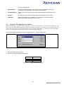
7.3
: Provides convenient buttons as shortcuts for the most frequently used menu
commands. The Help Button is the short-cut for Help\Index.
Setup the Debugging Environment
Before downloading a program to the LCEVB-SH1, you need to set up the user system for your application. The
Device type in LCEVB-SH1 Configuration Dialog-box needs to be setup. This leads to Device Memory Mapping
selection for the respective device automatically. Take note that LCEVB-SH1 is a common tool for current SH1
Series. The configuration of this setup is for information during debugging.
To set up the target configuration choose Configure Platform… from the Setup menu.:
Figure 7-4
Target Configuration Dialog-box
• Setup the option as shown below.
• Click OK to change the target configuration.
Option
Device
Mode
Table 7-1
Value
SH7034
Target
Target Configuration option
30
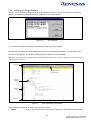
7.4
Memory Mapping
The next step is to open the Memory Mapping Window, select View then Memory Mapping Window. Alternatively,
click on the Mapping Speed-button:
Figure 7-5
Memory Mapping window Icon
The Memory Mapping window shown in the following figure is displayed:
Figure 7-6
Memory Mapping Window
The Target Device Configuration shows the following:
Memory
Description
Reserved Area
Internal IO
Internal RAM
Internal ROM
MCU unused & reserved area
MCU on-chip Input / Output port registers
MCU on-chip random access memory
MCU on-chip read only memory
Table 7-2
Target Device Configuration Description
In the Memory Mapping Window, the following memory attribution description:
Access Type
Description
On-Chip Read-write
On-Chip Read-only
On-Chip Guarded
User Read-write
User Read-only
User Guarded
Emulation RAM memory.
Emulation ROM memory.
No access allowed.
External RAM memory.
External ROM memory.
No access allowed.
Table 7-3
Target Memory Attribute
31
7.5
User Target Program Downloading
Once the LCEVB-SH1 is properly configured you can download the User Target Program (object program) you
want to debug.
First load the SYSROF-format object file (file extension .abs), as follows:
• Choose Load Program from the File menu, or click the Load program speed-button in the toolbar.
Figure 7-7
File-open speed-button
• Select the file tutorial.abs, in the \progra~1\hitach~1\sh1_tut directory, and click OK.
Figure 7-8
File-open Dialog-box
When the file has been loaded the dialogue box shown in the following figure displays information about the
memory areas that have been filled with the program code:
Figure 7-9
User Target Program downloaded Information
Note that all the code lies within the on-chip ROM.
• Click OK to continue.
32
7.6
Displaying User Target Program code
HDI allows you to debug a program at source level, so that you can see a listing of the program alongside the
disassembled code as you debug. To do this you need to read in a copy of the source program from which the
object file was compiled.
• Choose Program Window… from the View menu, or click the Program window button in the toolbar.
You will be prompted for the C source file corresponding to the object file you have loaded:
• Select tutorial.c and click OK to display the program window:
Figure 7-11
User Target Program Source Code window
• If necessary choose Font option from the Customise submenu on the Setup menu to choose a font and size
suitable for your computer.
33
7.7
Using Breakpoint (PC Breakpoint)
The simplest debugging aid is the PC breakpoint (Program breakpoint), which lets you halt execution when a
particular point in the program is reached. You can then examine the state of the MCU and memory at that point in
the program.
7.7.1
Setting PC Breakpoint
The program window provides a very simple way of setting a PC breakpoint. For example, set a breakpoint at
address H’0A00401A as follows:
• Double-click in the Break column on the line containing address H’0A00401A:
Figure 7-12
Setting a PC Breakpoint
The word Break (at the Break column) will be displayed there to show that a program breakpoint is set at that
address.
7.8
Executing User Target Program
To run the program from reset:
• Choose Go Reset from the Run menu, or click the Go Reset speed-button in the toolbar:
Figure 7-13
Go Reset speed-button
The program will be executed up to the breakpoint you inserted, and the statement will be highlighted in the
program window to show that the program has halted
34
Figure 7-14
Program (PC) Break
The message “Break = PC Breakpoint” is displayed in the status bar to show the cause of the break.
You can also see the cause of the last break in the System Status window.
• Choose Status Window from the View menu, or click the Status window button in the toolbar:
Figure 7-15
Status speed-button
Figure 7-16
Status window
The Cause of last break line shows that the break was a Program (PC) Break.
7.9
Examining Registers
While the program is halted you can examine the contents of the MCU registers. These are displayed in the
Registers window.
• Choose Registers window from the View menu, or click the Registers window speed-button in the toolbar:
Figure 7-17
Register speed-button
35
Figure 7-18
Register window
As expected, the value of the program counter (PC), is the same as the highlighted statement, H'0A00401A. Note
that during the execution of User Target Program, Emulation control is totally handed over to LCEVB-SH1
hardware. Thus, HDI has lose all control of the LCEVB-SH1 until it break (by PC breakpoint or by pressing
RESET/NMI button) where control is once again back with HDI.
You can also change the MCU registers from the Registers window. For example, to change the value of the PC:
• Double-click PC in the Register window.
The Register-PC Edit dialog-box allows you to edit the value.
Figure 7-19
Register-PC Edit Dialog-box
• Edit the value to H'0A004000, the starting address of the User Target Program, and click OK.
The yellow-highlighted bar will move to the new address in the program window (Tutorial.c) to show current
program counter value.
• Choose Go from the Run menu, or click the Go speed-button in the toolbar, to execute up to the breakpoint
again.
36
Figure 7-20
7.10
Go speed-button
Reviewing PC Breakpoints
You can see a list of all PC breakpoints set in the program in the Breakpoint window.
• Choose Breakpoint Window from the View menu, or click the Breakpoint Window speed-button in the toolbar:
Figure 7-21
Breakpoint window speed-button
The Breakpoint window also allows you to enable and disable individual breakpoint, define new breakpoints, and
delete breakpoints. Below shows the breakpoints set at several location besides address H’0A00401A previously
set:
Figure 7-22
Breakpoint window
Note that Symbol is actual address location. In another words, valid Labels/Symbols can be entered in the B Break
Address entry:
Figure 7-23
Breakpoint window Add Dialog-box
37
Before proceeding remove the breakpoint as follows:
• Highlight (move black-highlight bar) the breakpoint with address H’0A00401A and click Delete.
• Close the Breakpoint window.
7.11
User Memory Monitoring
You can monitor the behavior of User Target Program by:
• Examining content of the User memory
• Displaying variables’ content used
7.11.1 Viewing User Memory
You can view the contents of User Memory in the Memory window. For example, to view the memory
corresponding to the array section1 in ASCII:
• Choose Memory Window… from the View menu, or click the Memory Window button in the toolbar.
Figure 7-24
Memory window speed-button
• Enter section1 in the Address field, and set Format to ASCII.
Figure 7-25
Memory window Open Dialog-box
• Click OK to open the Memory window showing the specified area of memory.
Figure 7-26
Memory window in ASCII format start from address section1
38
• Leave the Memory window open so that you can monitor the contents of the array section1.
7.12
Watch Window
As you step through a program it is useful to be able to watch the Variables’ content used change according. in
your program, to verify that they change in the way that you expected. For example, set a watch on the structure
variable section1, declared at the beginning of the program, using the following procedure:
• Scroll up in the program window until you see the line:
.
.
.
main( )
{
count = 0;
for ( ; ; )
{
sort(section1, NAME);
count++;
.
.
.
• Place the blinking cursor in the word section1 in the program window.
• Click on the right mouse button in the program window to display a pop-up menu, and choose Instant Watch…:
Figure 7-27
Program window Popup menu
• The Instant Watch window will be displayed:
Figure 7-28
Instant Watch Dialog-box
• Click Add Watch to add the variable to the Watch window. Note, double-click on the Symbols (e.g. section1)
with the ‘+’ at the left of Symbol/Label will expand that Symbol/Label further if it has finer detail.
39
Figure 7-29
Watch window
You can also add a watch to the Watch window by specifying its name. Use this method to add a Watch on the
variable count as follows:
• Click right mouse button in Watch window and choose Add Watch… from the pop-up menu.:
Figure 7-30
Watch window Popup menu
The Add Watch dialogue box appears:
Figure 7-31
Watch window Add Watch Dialog-box
• Type the Symbol/Label to watch and click OK will show the similar display as shown in Figure 7-28.
40
7.12
Local Variable Watch
Local Variable window is treated different from Watch window. Content of Watch window is determinate by User,
while content of Local Variable window will only appear once User Target Program execution reach function that
has variables within the scope of the function.
You can watch variables local in a function using the Local Variables window. For example, we will examine the
local variables in the function sort.
• Open the Locals window by choosing Local Variable window from the View menu.
Note again that the Locals window will be empty if the local variable declarations have not yet been executed.
The Local Variable window will now show the local variables with their values once execution has reach the
function sort:
Figure 7-32
•
Local Variable window
Double-click the ‘+’ in front of the variable worklist in the Local Variable window to display the individual
elements of the array worklist.
7.13
Stepping User Target Program
LCEVB-SH1 provides a range of options for single stepping through a program, executing an instruction or
statement at a time. The stepping commands is listed below:
Command
Description
Step In
Step…
Executes every statement, including statements within functions.
Allows you to step repeatedly at a specified rate.
Table 7-4
Single Step Command
7.13.1 Single Step
Single step by selecting Step In… in Run menu or click on the Step-in speed-button at the Toolbar:
Figure 7-33
Step-in speed-button
41
• Observe that the PC (Register window) is incremented each time the Step-in speed-button is clicked. The PC
always points to the current instruction to be executed by MCU. Note the yellow-highlight bar in the program
window also indicate the current location of PC.
7.14
Save Session
Before exiting it is good practice to save your session, so that you can resume with the same ALE300L emulator
and HDI configuration at your next debugging session.
• Choose Save Session… from the File menu.
• Choose Exit from the File menu to exit from HDI.
7.14
What Next?
This tutorial has introduced you to some of the key features of the ALE300L emulator, and their use in conjunction
with the HDI. By combining the emulation tools provided in the ALE300L emulator you can perform extremely
sophisticated debugging, allowing you to track down hardware and software problems very efficiently by precisely
isolating and identifying the conditions under which they occur.
42
Section 8: Troubleshooting
Communication Problems
1
Verify the communication channel
• Is the Communication Port used by another device?
• Right Communication Port (COM1/COM2) selected?
• Right Communication Baud Rate (57,600bps) supported by Host PC
2
Power supply not switched on, or not connected, or connected loosely to the LCEVB-SH1.
Check the power LED on the LCEVB-SH1.
3
The PC interface cable is not correctly connected between the PC interface board and the
LCEVB-SH1.
5
Wrong PC interface/serial cable used? PC Interface /serial cable could be faulty?
Verify that pins 2 and 3 of each end of cable are connected to each other respectively.
6
Is the target system drawing too much current?
User Target System connected is drawing to much current.
No Power
1
The fuse may have been blown due to mishandling such as shorting of VCC and Ground, or
drawing of too much current from target system.
Simply replace the 1A fuse located beside the main power switch.
Note: Please investigates the cause before replacing the fuse.
Target system not working
1
Check User voltage
•
2
Running at LCEVB-SH1 supply(5 Volt)
Target may be drawing too much current from the LCEVB-SH1
Check the clock used to perform emulation
• Only one of the on-board clock source can be used at any one time.
43
Appendix A: Frequently Asked Questions
This section contains a list of frequently asked questions about developing and evaluating programs using the
LCEVB-SH1.
1. How do I write to the SH serial ports?
See the tutorial examples. Refer to the also Appendix C.
2. Why is RAM on the LCEVB-SH1 at such a high address?
The LCEVB-SH1 RAM starts at H'A000000. Since the monitor must reside at 0 (area 0) to provide for system bootup, system RAM must be located somewhere else. Areas 0 and 2 share internal wait-state generation facilities, so
area 2 is a logical place for RAM. Area 2 starts at location H'2000000, but to access it as word-wide, it must be
addressed starting at H'A000000.
3. Can LCEVB-SH1 RAM be accessed at a different address? Why do I have trouble with the RAM at
H'200000?
Conceptually, memory that is in SH area 2 is addressable at both address H'2000000 and H'A000000. The correct
addressing considering the LCEVB-SH1’s hardware memory configuration is starting at H'A000000.The LCEVBSH1 RAM is word-wide. If you address it at H'2000000, you’ll be telling the SH that it is byte-wide. In hardware
terms, for purely 8-bit accesses, the SH signal LBS will never go low, so half the RAM memory on the board will not
be used.
4. Why doesn’t the monitor use SH on-board RAM?
On-board SH RAM is the fastest possible, being accessible in 32-bit chunks without wait states. Committing this
RAM to the monitor might interfere with using this area for full-speed benchmarks.
Since monitor source is included with the LCEVB-SH1 kit, users are free to allocate onboard RAM for this use.
5. Why does the LCEVB-SH1 have word-wide instead of byte-wide RAM?
Word-wide accesses are faster. This choice was an inexpensive way of providing faster program execution.
6. My program (or the monitor) is crashing randomly. What might be wrong?
Check these possibilities:
• Check that your program isn’t affecting the monitor RAM area. Use the CMON status command to find the
current limit of monitor RAM use. Locate the code, data, and stack above that area.
• Check that there is actually RAM in the areas you are using.
• The monitor may work erratically if RAM is unavailable or only partly available, that is if one or both RAM ICs
are not correctly plugged into the board.
• Make sure your power supply is more than sufficient for the needs of the LCEVB-SH1. Power supplies operating
at or near their limits can sometimes cause programs to operate strangely.
• Make sure that the stack pointer (R15) is pointing to RAM. A simple way of doing this is to reset the monitor.
7. How can I time my benchmarks?
Every benchmark is different. One approach is to use an I/O bit, for example, by setting it low upon entering the
code-of-interest and high again when leaving.
44
8. When must I use HINT and when can I use, say, PROCOMM® with CMON?
The only time you must use HINT is when you want to use the Save (“SV”) command. Most users won’t have any
reason to upload an s-record representation of an LCEVB-SH1 memory region to a host computer, so this should
be no problem. Otherwise, for all commands, you can use almost any terminal emulator.
9. So what’s the problem with using Save (“SV”) and—if that’s a problem—how does Load work?
The problem is specifying a filename on the host computer. Barring the use of a full-blown protocol like ZMODEM,
there’s no standard way that CMON can inform the host of what file name to use for the data.
There is one somewhat awkward way of using SV with any terminal emulator, but this requires you to start up your
terminal emulator’s ASCII capture before invoking SV in CMON. You’ll undoubtedly have to enter a file name.
Load works smoothly because you can invoke the “L” command in CMON, then start up your emulator’s ASCII
download facility.
10. Besides that, why use HINT?
It would be very difficult to document setups for using CMON with every terminal emulator commonly used. By
supplying an easy-to-use baseline terminal emulator, we can ask you “What happens when you use HINT” rather
than trying to figure out your terminal emulator setup.
11. Does an application program need to establish its own stack for proper operation on the LCEVB-SH1?
Trivial programs don’t. There’s room on the monitor stack for user programs, and we’ve used simple programs
without declaring a distinct user stack, but we’d prefer that you establish your own stack. See the tutorials for
examples.
12. I just entered a very simple program loop using the CMON assembler and it crashed for no reason I can see.
What’s going on?
If your program ends with a branch, and there’s garbage in memory following the branch, you’ve likely found an
often-misunderstood SH feature: “delayed branches”. In order to be as efficient as possible, in the case of some
program branches, the instruction following the branch is also executed even if the branch is taken. The BRA
instruction is one of these. If you write a simple loop, it is likely to end with a BRA back to beginning, and it’s likely
that the garbage following the BRA caused the problem. You’ll crash somehow, possibly generating an exception
and a message like “INVALID INSTRUCTION” or “INVALID SLOT” or “CPU BUS ERROR”. A full discussion of this
subject is beyond the scope of this manual. An excellent rule of thumb is: when in doubt, follow all branches with
innocuous instructions (such as NOPs).
13. My benchmark shows that the SH doesn’t run as fast as I think it should. Why?
For maximum flexibility, CMON accepts the default setting of WCR3, that is, the LCEVB-SH1 automatically inserts
4 wait states into area 0 and area 2 accesses. This will certainly make the SH run slower. You can adjust the value
of the A02LW1 and A02LW0 bits in WCR3, consistent with the operating speed of the SH processor and the
memory currently installed.
45
Appendix B: Assembler Commands
This appendix lists assembler command syntax, sorted according to different categories and types.
B.1
Legend
Table B.1 lists command syntax abbreviations and their meanings.
Abbreviation
Meaning
Rn
A numbered register
Rm
Another numbered register
#imm
Immediate data
Disp
Displacement
disp8
8-bit displacement
disp12
12-bit displacement
Table B.1: Command Syntax Abbreviations
B.2
Commands Sorted Alphabetically
Available assembler instruction listing:
add #imm,Rn
add Rm,Rn
addc Rm,Rn
addv Rm,Rn
and #imm,R0
and Rm,Rn
and.b #imm,@(R0,GBR)
bf disp8
bra disp12
bsr disp12
bt disp8
clrmac
clrt
cmp/eq #imm,R0
cmp/eq Rm,Rn
mov Rm,Rn
mov.b Rm,@(R0,Rn)
mov.b Rm,@-Rn
mov.b Rm,@Rn
mov.b @(disp,Rm),R0
mov.b @(disp,GBR),R0
cmp/ge Rm,Rn
cmp/gt Rm,Rn
cmp/hi Rm,Rn
cmp/hs Rm,Rn
cmp/pl Rn
cmp/pz Rn
cmp/str Rm,Rn
div0s Rm,Rn
div0u
div1 Rm,Rn
exts.b Rm,Rn
exts.w Rm,Rn
extu.b Rm,Rn
extu.w Rm,Rn
jmp @Rn
mov.w @Rm,Rn
mov.w R0,@(disp,Rm)
mov.w R0,@(disp,GBR)
mova @(disp,PC),R0
movt Rn
muls Rm,Rn
46
jsr @Rn
ldc Rn,GBR
ldc Rn,SR
ldc Rn,VBR
ldc.l @Rn+,GBR
ldc.l @Rn+,SR
ldc.l @Rn+,VBR
lds Rn,MACH
lds Rn,MACL
lds Rn,PR
lds.l @Rn+,MACH
lds.l @Rn+,MACL
lds.l @Rn+,PR
mac.w @Rm+,@Rn+
mov #imm,Rn
shlr8 Rn
sleep
stc GBR,Rn
stc SR,Rn
stc VBR,Rn
stc.l GBR,@-Rn
mov.b @(R0,Rm),Rn
mov.b @Rm+,Rn
mov.b @Rm,Rn
mov.b R0,@(disp,Rm)
mov.b R0,@(disp,GBR)
mov.l Rm,@(disp,Rn)
mov.l Rm,@(R0,Rn)
mov.l Rm,@-Rn
mov.l Rm,@Rn
mov.l @(disp,Rn),Rm
mov.l @(disp,GBR),R0
mov.l @(disp,PC),Rn
mov.l @(R0,Rm),Rn
mov.l @Rm+,Rn
mov.l @Rm,Rn
mov.l R0,@(disp,GBR)
mov.w Rm,@(R0,Rn)
mov.w Rm,@-Rn
mov.w Rm,@Rn
mov.w @(disp,Rm),R0
mov.w @(disp,GBR),R0
mov.w @(disp,PC),Rn
mov.w @(R0,Rm),Rn
mov.w @Rm+,Rn
B.3
mulu Rm,Rn
neg Rm,Rn
negc Rm,Rn
nop
not Rm,Rn
or #imm,R0
or Rm,Rn
or.b #imm,@(R0,GBR)
rotcl Rn
rotcr Rn
rotl Rn
rotr Rn
rte
rts
sett
shal Rn
shar Rn
shll Rn
shll16 Rn
shll2 Rn
shll8 Rn
shlr Rn
shlr16 Rn
shlr2 Rn
stc.l SR,@-Rn
stc.l VBR,@-Rn
sts MACH,Rn
sts MACL,Rn
sts PR,Rn
sts.l MACH,@-Rn
sts.l MACL,@-Rn
sts.l PR,@-Rn
sub Rm,Rn
subc Rm,Rn
subv Rm,Rn
swap.b Rm,Rn
swap.w Rm,Rn
tas.b @Rn
trapa #imm
tst #imm,R0
tst Rm,Rn
tst.b #imm,@(R0,GBR)
xor #imm,R0
xor Rm,Rn
xor.b #imm,@(R0,GBR)
xtrct Rm,Rn
Commands Sorted by Type
B.3.1 Data Transfer
mov #imm,Rn
mov Rm,Rn
mov.b Rm,@(R0,Rn)
mov.b Rm,@-Rn
mov.b Rm,@Rn
mov.b @(disp,Rm),R0
mov.b @(disp,GBR),R0
mov.b @(R0,Rm),Rn
mov.b @Rm+,Rn
mov.b @Rm,Rn
mov.b R0,@(disp,Rm)
mov.b R0,@(disp,GBR)
mov.l Rm,@(disp,Rn)
mov.l Rm,@(R0,Rn)
mov.l Rm,@-Rn
mov.l Rm,@Rn
mov.l @(disp,Rn),Rm
mov.l @(disp,GBR),R0
mov.l @(disp,PC),Rn
mov.l @(R0,Rm),Rn
mov.l @Rm+,Rn
mov.l @Rm,Rn
mov.l R0,@(disp,GBR)
mov.w Rm,@(R0,Rn)
mov.w Rm,@-Rn
mov.w Rm,@Rn
47
mov.w @(disp,Rm),R0
mov.w @(disp,GBR),R0
mov.w @(disp,PC),Rn
mov.w @(R0,Rm),Rn
mov.w @Rm+,Rn
mov.w @Rm,Rn
mov.w R0,@(disp,Rm)
mov.w R0,@(disp,GBR)
mova @(disp,PC),R0
movt Rn
swap.b Rm,Rn
swap.w Rm,Rn
xtrct Rm,Rn
B.3.2 Arithmetic Operations
add #imm,Rn
add Rm,Rn
addc Rm,Rn
addv Rm,Rn
cmp/eq #imm,R0
cmp/eq Rm,Rn
cmp/ge Rm,Rn
cmp/gt Rm,Rn
cmp/hi Rm,Rn
cmp/hs Rm,Rn
cmp/pl Rn
cmp/pz Rn
cmp/str Rm,Rn
div0s Rm,Rn
div0u
div1 Rm,Rn
exts.b Rm,Rn
exts.w Rm,Rn
extu.b Rm,Rn
extu.w Rm,Rn
mac.w @Rm+,@Rn+
muls Rm,Rn
mulu Rm,Rn
neg Rm,Rn
negc Rm,Rn
sub Rm,Rn
subc Rm,Rn
subv Rm,Rn
or #imm,R0
or Rm,Rn
or.b #imm,@(R0,GBR)
tas.b @Rn
xor #imm,R0
xor Rm,Rn
xor.b #imm,@(R0,GBR)
shar Rn
shll Rn
shll2 Rn
shll8 Rn
shll16 Rn
shlr Rn
shlr2 Rn
shlr8 Rn
shlr16 Rn
B.3.3 Logical
and #imm,R0
and Rm,Rn
and.b #imm,@(R0,GBR)
not Rm,Rn
B.3.4 Shift/Rotate
rotl Rn
rotr Rn
rotcl Rn
rotcr Rn
shal Rn
B.3.5 Branches
bf disp8
bt disp8
bra disp12
bsr disp12
jmp @Rn
jsr @Rn
rts
48
B.3.6 System Control
Clrt
Clrmac
Ldc Rn,GBR
ldc Rn,SR
ldc Rn,VBR
ldc.l @Rn+,GBR
ldc.l @Rn+,SR
ldc.l @Rn+,VBR
lds Rn,MACH
lds Rn,MACL
lds Rn,PR
lds.l @Rn+,MACH
lds.l @Rn+,MACL
lds.l @Rn+,PR
nop
rte
sett
sleep
stc GBR,Rn
stc SR,Rn
stc VBR,Rn
stc.l GBR,@-Rn
stc.l SR,@-Rn
stc.l VBR,@-Rn
49
sts MACH,Rn
sts MACL,Rn
sts PR,Rn
sts.l MACH,@-Rn
sts.l MACL,@-Rn
sts.l PR,@-Rn
trapa #imm
tst #imm,R0
tst Rm,Rn
tst.b #imm,@(R0,GBR)
Appendix C: Mini-project
This section contains the schematic for a mini DC motor project that can be constructed and connected with the
LCEVB-SH1. The purpose of this project is to test the PWM function of the SH1 and also it’s Input and output pin.
Also provided is the SH1 C program required to run it. This C program can be compiled using the SuperH RISC
engine C/C++ Compiler, Assembler, Optimizing Linkage Editor. The Object file will then have to be converted to Srecord using the H series Linker and the S record converter before it can be downloaded to the LCEVB-SH1.
When invoking the Linker, please take note that user program can only start at H’A004000. Thus it is required to
specified the start address of the program section. The C source program of the Motor-control can be found in
project directory.
C.1
Bill of Material
Item
Quantity
• Push Button switch (normally
open)
• DC Motor
• 7 segment Display (Common
anode)
• Resistor 330Ω
• 470Ω
• 1.2KΩ
• 3.9KΩ
• 22KΩ
• Capacitor 0.1µF
• Transistor 2N2222A
• BC131
• Diode 1N4001
• LED (RED)
• (GREEN)
• 74HC04
• Buzzer
02
01
01
07
01
01
02
02
02
01
01
01
01
01
01
01
Table E.1: Bill of Material for Mini Project
C.2
Operation
The program starts out by displaying 1 to 10 on the 7 segment display. After which depressing S10 will increment
the 7 segment display by 1 to a maximum of 5 and depressing S11 will decrement the display by 1 to a minimum of
0. Respectively the duty cycle of the PWM driving the motor will increase or decrease by 1% starting from 4% to a
maximum of 8% corresponding to the value displayed . Depressing both S10 and S11 causes motor to stop.
50
C.3
Software Listing
/*
----------------------------------------------------------------Program Name
: motor.c
Date
: 20 Mar 97
----------------------------------------------------------------- */
#include <machine.h>
#include <iosh7030.h>
/*
----------------------------------------------------------------Constants
----------------------------------------------------------------- */
#define delay_constant 80160
/* delay of 0.1 sec */
unsigned char display_table[11]={0x40,0x79,0x24,0x30,0x19,0x12,
0x02,0x78,0x00,0x18,0x7F};
unsigned short pwm_table[11]={0,160,200,240,280,320};
/*
/* 0,4,5,6,7,8 */
----------------------------------------------------------------Global Variables
----------------------------------------------------------------- */
unsigned char motor_speed=0;
unsigned char past_motor_speed=0;
main()
{
/*motor speed*/
/*previous motor speed*/
/* main program */
init_ports();
init_timers();
count();
while (1)
/* infinite loop */
{
get_data();
out_motor();
}
}
/* End Main */
/* ---------------------------------------------------------------Routine : out_motor()
Purpose : output to motor
Note
: kick starts stationary motor
-------------------------------------------------------------- */
out_motor()
{
if ( (past_motor_speed == 0) && (motor_speed == 1) )
{
ITU_GRB1 = 600; /* kick-starts */
delay20ms();
}
ITU_GRB1 = pwm_table[motor_speed];
/* o/p to motor */
}
51
/* ---------------------------------------------------------------Routine : get_data()
Purpose : read PC0 & PC1 using software debouncing
-------------------------------------------------------------- */
get_data()
{
unsigned char temp,temp1,temp2;
unsigned char stable = 1;
while(stable)
{
temp = (PCDR & 0x03);
delay20ms();
temp1 = (PCDR & 0x03);
delay20ms();
temp2 = (PCDR & 0x03);
if ( (temp == temp1) && (temp1 == temp2) && (temp != 0x03) )
{
stable = 0;
beep();
}
}
past_motor_speed = motor_speed; /* update past_motor_speed */
switch(temp)
{
case 0x00:
/* both switches are ON */
motor_speed = 0;
break;
case 0x02:
/* PC0 is ON */
if (motor_speed >= 5)
{
motor_speed = 5;
}
else
{
motor_speed++;
}
break;
case 0x01:
/* PC1 is ON */
if (motor_speed <= 1)
{
motor_speed = 0;
}
else
{
motor_speed--;
}
break;
default:
motor_speed = 0;
break;
}
/* End Switch */
PBDR = ( (PBDR & 0xFF80) | display_table[motor_speed] );
while ( temp == (PCDR & 0x03) ) /* check for switch to be released */
{
delay20ms();
52
}
}
PBDR = (PBDR & 0xFF7F);
/* End get_data() */
/* off buzzer */
/* ---------------------------------------------------------------Routine : count()
Purpose : display 0 to 9 at 0.2 second interval
-------------------------------------------------------------- */
count()
{
int
display_count;
for (display_count = 0 ; display_count < 11 ; display_count++)
{
PBDR = display_table[display_count];
d_xx(10);
/* delay = 10 x 20ms = 0.2 sec */
}
}
/* ---------------------------------------------------------------Routine : beep()
Purpose : set PB7 => on buzzer
-------------------------------------------------------------- */
beep()
{
PBDR = (PBDR | 0x0080); /* set PB7 */
}
/* ---------------------------------------------------------------Routine : delay20ms()
Purpose : generate a software delay of 20ms
-------------------------------------------------------------- */
delay20ms()
{
int
dvar1;
for (dvar1 = 0 ; dvar1 < 16000 ; dvar1 ++ );
}
/* ---------------------------------------------------------------Routine : d_xx(count)
Purpose : generate a delay in multiples of 20ms using ITU_TCNT0
-------------------------------------------------------------- */
d_xx(count)
int count;
{
int delay_var;
unsigned char temp;
ITU_TCNT0 = 0;
ITU_TSTR = (ITU_TSTR | 0x01);
/* starts counting from 0 */
/* starts ITU_TCNT0 */
for (delay_var = 0 ; delay_var <= count ; delay_var ++)
{
while ( (temp = (ITU_TSR0 & 0x01) ) == 0)
/*check for IMFA = 1*/
{
}
ITU_TSR0 = (ITU_TSR0 & 0xF8);
/* IMFA flag = 0 */
}
ITU_TSTR = (ITU_TSTR & 0xFE);
/* stop ITU_TCNT0 */
return(0);
}
/* ---------------------------------------------------------------Routine : delay(count)
53
Purpose : generate a software delay in multiples of 20ms
-------------------------------------------------------------- */
delay(count)
int count;
{
int delay_var,ddd;
for (ddd=0 ; ddd != count ;ddd ++)
{
for (delay_var=0 ; delay_var<=delay_constant ; delay_var++);
}
return(0);
}
/* ---------------------------------------------------------------Routine : init_ports()
Purpose : initialize Ports A and B
Port Configuration :
a. PA10 : TIOCA0
b. PB0 <-> PB6 : output to drive 7-segment LED
-------------------------------------------------------------- */
init_ports()
{
PFC_PACR1
PFC_PACR2
PFC_PAIOR
PFC_PBCR1
PFC_PBCR2
PFC_PBIOR
}
=
=
=
=
=
=
0x0020;
0xBF55;
0xFFFF;
0x0000;
0x0000;
0xFFFF;
/*
/*
/*
/*
/*
/*
PA15
PB7
PB15
PB15
PB7
PB15
<->
<->
<->
<->
<->
<->
PA8
PB0
PB0
PB8
PB0
PB0
except PA10: general purpose I/O */
: general purpose I/O */
: all output */
: general purpose I/O */
: general purpose I/O */
: all output */
/* ---------------------------------------------------------------Routine : init_timers()
Purpose : initialize timers 0 & 1
-------------------------------------------------------------- */
init_timers()
{
ITU_TSNC = 0x00;
ITU_TMDR = 0x82;
ITU_GRA1 = 4000;
ITU_GRB1 = 0;
/* All channels to function independently */
/* TCNT0 : normal operation */
/* TCNT1 : PWM operation */
/* base = 4000 */
ITU_TCR0 = 0xA3;
/*
ITU_TCNT0 is cleared by output compare match A
Select internal clock /8
1 period = 8/20 MHz = 400 ns */
ITU_TIOR0 = 0x88;
/*
Select output compare operation with pin output disabled */
ITU_GRA0 = 50000;
/* 50000 x 400 ns = 20 ms */
ITU_TCR1 = 0x23;
/* TCNT1 is cleared by GRA compare match */
ITU_TSTR = (ITU_TSTR | 0x02);
/* starts ITU_TCNT1 */
}
exit()
{
trapa(0);
}
int __main() {}
/* now required by compiler; see release notes */
54
Appendix D: Schematic Diagram of Mini-project
55
Appendix E: Schematic Diagram of LCEVB-SH1
VCC
2(7)
VCC
OP
GND
NC
3(8)
3
1
2
1
OSC
43
15
70
75
77
83
84
99
EXTAL
J2
Y1
1
2
XTAL
79
RESET
20MHz
C3
22 pF
VCC
U1 SH7032
VCC
OSCILLATOR CIRCUITRYJ1
OSC1
4(14)
VCC
VCC
VCC
VCC
VCC(VPP)
VCC
VCC
VCC
RES
AVCC
VCC
85
J3
2
C1
86
76
3
GND Vcc
R
1
80
81
82
RESET
nc
3
73
EXTAL
C7
0.01uF
74
XTAL
VCC
MD0
MD1
MD2
NMI
CIRCUITRY
XTAL
R1 10K
J6
Momentary
1
U3A
3
2
S2
A[0..21]
UNMI
3
U3A
1
3
2
74HC00
2
1
NMI
74HC00
CONTROL
VCC
J7
3
MD[0..2]
2MD2
1
J8
3
MODE
SELECTOR
2MD1
1
J9
3
1
2MD0
VCC
D1
GREEN LED
CONTROL
PB[0..15]
LED CIRCUITRY
J10
PA15 3
PB15 1
2
9
AVREF
A0
A1
A2
A3
A4
A5
A6
A7
A8
A9
A10
A11
A12
A13
A14
A15
A16
A17
A18
A19
A20
A21
23
24
25
26
27
28
29
30
32
33
34
35
36
37
38
39
41
42
44
45
46
47
CS0
48
CS1
49
CS2
50
CS3
51
PA0
53
PA1
54
PA2
55
PA3
56
PA4
57
PA5
58
PA6
59
PA7
60
PA8
62
PA9
63
PA10 64
PA11 65
PA12 66
PA13 67
PA14 68
PA15 69
CK
71
WDTOVF/ 78
AVSS
91
2
3
AVSS
1
PC[0..7]
EXTAL
VCC
R2
10K
3
J5
MD0
MD1
MD2
1
2
S1
Momentary
AVCC
VCC
1
NMI
MD[0..2]
RESET CIRCUITRY
U2
DS1233
2
C6
0.01uF
3
J4
2
C5
10uF
C4
22 pF
NMI
C2
0.01uF
10uF
AVREF
1
A0(HBS)
A1
A2
A3
A4
A5
A6
A7
A8
A9
A10
A11
A12
A13
A14
A15
A16
A17
A18
A19
A20
A21
CSO
CS1/CASH
CS2
CS3/CASL
PA0/CS4/TIOCA0
PA1/CS5/RAS
PA2/CS6TICBO
PA3/CS7/WAIT
PA4/WRL(WR)
PA5/WRH(LBS)
PA6/RD
PA7/BACK
PA8/BREQ
PA9/AH/IRQOUT/ADTRG
PA10/DPL/TIOCA1
PA11/DPH/TIOCB1
PA12/IRQ0/DACK0/TCLKA
PA13/IRQ/DREQ0/TCLKB
PA14/IRQ2/DACK1]
PA15/IRQ3/DREQ1
CK
WDTOVF
PC0/AN0
PC1/AN1
PC2/AN2
PC3/AN3
PC4/AN4
PC5/AN5
PC6/AN6
PC7/AN7
PB0/TP0/TIOCA2
PB1/TP1/TIOCB2
PB2/TP2/TIOCA3
PB3/TP3/TIOCB3
PB4/TP4/TIOCA4
PB5/TP5/TIOCB4
PB6/TP6/TOCXA4/TCLKC
PB7/TP7/TOCXB4/TCLKD
PB8/TP8/RXD0
PB9/TP9/TXD0
PB10/TP10/RXD1
PB11/TP11/TXD1
PB12/TP12/IRQ4/SCK0
PB13/TP13/IRQ5/SCK1
PB14/TP14/IRQ6
PB15/TP15/IRQ7
87
88
89
90
92
93
94
95
PC0
PC1
PC2
PC3
PC4
PC5
PC6
PC7
PB[0..15]
PB0
PB1
PB2
PB3
PB4
PB5
PB6
PB7
PB8
PB9
PB10
PB11
PB12
PB13
PB14
PB15
97
98
100
101
102
103
104
105
107
108
109
110
111
112
1
2
D[0..15]
AD15
AD14
AD13
AD12
AD11
AD10
AD9
AD8
AD7
AD6
AD5
AD4
AD3
AD2
AD1
AD0
VSS
VSS
VSS
VSS
VSS
VSS
VSS
VSS
VSS
VSS
21
20
19
18
17
16
14
13
11
10
9
8
7
6
5
4
AD15
AD14
AD13
AD12
AD11
AD10
AD9
AD8
AD7
AD6
AD5
AD4
AD3
AD2
AD1
AD0
DECOUPLING CIRCUIT
3
12
22
31
40
52
61
72
106
96
VCC
C8
0.01uF
C9
0.01uF
R4
470
U3C
8
10
74HC00
Renesas System Solutions Asia Pte Ltd
Singapore Engineering Center
Size
Document Number
Date:
Friday, April 11, 2003
A3
56
Rev
ASH1EVB001-CPU
2.0
Sheet
1
of
6
D[0..15]
A[0..21]
U4
A0
A1
A2
A3
A4
A5
A6
A7
A8
A9
A10
A11
A12
A13
A14
A15
10
9
8
7
6
5
4
3
25
24
21
23
2
26
27
1
CS0
20
PA6/RD 22
U5
A0
A1
A2
A3
A4
A5
A6
A7
A8
A9
A10
A11
A12
A13
A14
A15
D0
D1
D2
D3
D4
D5
D6
D7
11
12
13
15
16
17
18
19
D0
D1
D2
D3
D4
D5
D6
D7
A1
A2
A3
A4
A5
A6
A7
A8
A9
A10
A11
A12
A13
A14
A15
PA5/LBS_N1
CE
OE
VCC
VCC
VSS
28
14
CS2
PA4/WR
10
9
8
7
6
5
4
3
25
24
21
23
2
26
1
U6
D0
D1
D2
D3
D4
D5
D6
D7
A0
A1
A2
A3
A4
A5
A6
A7
A8
A9
A10
A11
A12
A13
A14
11
12
13
15
16
17
18
19
D0
D1
D2
D3
D4
D5
D6
D7
U7A
3
2
20
27
22
74CT32
VCC
CS
WE
OE
VCC
PA6/RD
VSS
27C512
HM62256
28
14
A1
A2
A3
A4
A5
A6
A7
A8
A9
A10
A11
A12
A13
A14
A15
A0/HBS_N 4
CS2
PA4/WR
10
9
8
7
6
5
4
3
25
24
21
23
2
26
1
11
12
13
15
16
17
18
19
U7B
6
5
74CT32
20
27
22
D0
D1
D2
D3
D4
D5
D6
D7
VCC
CS
WE
OE
VCC
PA6/RD
VSS
28
14
HM62256
SRAM
EPROM
D0
D1
D2
D3
D4
D5
D6
D7
A0
A1
A2
A3
A4
A5
A6
A7
A8
A9
A10
A11
A12
A13
A14
SRAM
CONTROL
VCC
C10
0.01uF
C11
0.01uF
C12
0.01uF
C13
0.01uF
DECOUPLING CIRCUIT
Renesas System Solutions Asia Pte Ltd
Singapore Engineering Center
Size
Document Number
Date:
Friday, April 11, 2003
A3
57
Rev
ASH1EVB001-Memorys
1.0
Sheet
3
of
6
EXT POWER SUPPLY
VCC
J11
F1
D2
2
1
D3
1N4148
1
RED LED
+
Power Supply
3
U8
LM7805
VOUT
VIN
VCC
3
GND
FUSE
2
1
C14
100uF
C15
0.1uF
C16
0.1uF
2
JP1
C17
100uF
J12
Phono Jack
DC Adapter
Renesas System Solutions Asia Pte Ltd
Singapore Engineering Center
Size
A
Date:
58
Document Number
Rev
ASH1EVB001- Power Supply
Friday, April 11, 2003
2.1
Sheet
4
of
6
PB[0..15]
VCC
J15
PB11
1
1uF
2
1
2
3
1uF
4
C21
1uF
5
10
9
11
J17
PB9
1
2
12
C1+
C1-
V+
V-
2
1uF
C2-
R1IN
T2IN
T1OUT
R2OUT
R2IN
T1IN
R1OUT
MAX232A
C20
6
C2+
GND
PB10
C19
T2OUT
13
USER
14
8
7
5
9
4
8
3
7
2
6
1
J18
PB8
1
P1
5
9
4
8
3
7
2
6
1
15
1
J16
VCC
U9
16
C18
2
P2
HOST
VCC
C22
1uF
Renesas System SolutionsAsia Pte Ltd
DECOUPLING CIRCUIT
Singapore Engineering Center
Size
A
Date:
59
Document Number
Rev
ASH1EVB001-Serial Comms
Friday, April 11, 2003
1.0
Sheet
6
of
6
VCC
VCC
PB[0..15]
A[0..21]
AD[0..15]
USER1
PB15
2
4
6
8
10
12
14
16
18
20
22
24
26
28
30
32
34
36
38
40
42
44
46
48
50
AD0
AD1
AD2
AD3
AD4
AD5
AD6
AD7
AD8
AD9
AD10
AD11
AD12
AD13
AD14
AD15
A0
A1
A2
A3
A4
A5
A[0..21]
1
3
5
7
9
11
13
15
17
19
21
23
25
27
29
31
33
35
37
39
41
43
45
47
49
PB14
A6
A7
A8
A9
A10
A11
A12
A13
A14
A15
A16
A17
A18
A19
A20
A21
CS0
CS1
CS2
CS3
PA0
PA1
PA2
PA3
PIN HEADER 2X25
USER2
1
3
5
7
9
11
13
15
17
19
21
23
25
27
29
31
33
35
37
39
41
43
45
47
49
2
4
6
8
10
12
14
16
18
20
22
24
26
28
30
32
34
36
38
40
42
44
46
48
50
PIN HEADER 2X25
PA[0..15]
VCC
VCC
VCC
PA[0..15]
USER3
PA4
PA5
PA6
PA7
PA8
PA9
PA10
PA11
PA12
PA13
PA14
PA15
CK
WDTOVF
2
4
6
8
10
12
14
16
18
20
22
24
26
28
30
32
34
36
38
40
42
44
46
48
50
1
3
5
7
9
11
13
15
17
19
21
23
25
27
29
31
33
35
37
39
41
43
45
47
49
USER4
AVREF
AVSS
PC[0..7]
UNMI
PC0
PC1
PC2
PC3
PC4
PC5
PC6
PC7
PB0
PB1
PB2
PB3
PB4
PB5
PB6
PB7
PB8
PB9
PB10
PB11
PB12
PB13
PIN HEADER 2X25
PB[0..15]
1
3
5
7
9
11
13
15
17
19
21
23
25
27
29
31
33
35
37
39
41
43
45
47
49
2
4
6
8
10
12
14
16
18
20
22
24
26
28
30
32
34
36
38
40
42
44
46
48
50
AVCC
PIN HEADER 2X25
Renesas System Solutions Asia Pte Ltd
Singapore Engineering Center
Size
Document Number
Date:
Wednesday, February 10, 1999 Sheet
A3
60
Rev
ASH1EVB001-Connectors
2.1
5
of
6
Renesas Technology (Asia Sales Offices)
URL: http://www.renesas.com
LCEVB-SH1