1
CMOS 8-BIT MICROCONTROLLER
LC871A00 SERIES
USER’S MANUAL
http://onsemi.com
REV : 1.02
ON Semiconductor
Digital Solution Division
Microcontroller & Flash Business Unit
ON Semiconductor and the ON logo are registered trademarks of Semiconductor Components Industries, LLC (SCILLC). SCILLC owns the rights to a number
of patents, trademarks, copyrights, trade secrets, and other intellectual property. A listing of SCILLC’s product/patent coverage may be accessed at
www.onsemi.com/site/pdf/Patent-Marking.pdf. SCILLC reserves the right to make changes without further notice to any products herein. SCILLC makes no
warranty, representation or guarantee regarding the suitability of its products for any particular purpose, nor does SCILLC assume any liability arising out of the
application or use of any product or circuit, and specifically disclaims any and all liability, including without limitation special, consequential or incidental
damages. “Typical” parameters which may be provided in SCILLC data sheets and/or specifications can and do vary in different applications and actual
performance may vary over time. All operating parameters, including “Typicals” must be validated for each customer application by customer’s technical experts.
SCILLC does not convey any license under its patent rights nor the rights of others. SCILLC products are not designed, intended, or authorized for use as
components in systems intended for surgical implant into the body, or other applications intended to support or sustain life, or for any other application in which
the failure of the SCILLC product could create a situation where personal injury or death may occur. Should Buyer purchase or use SCILLC products for any
such unintended or unauthorized application, Buyer shall indemnify and hold SCILLC and its officers, employees, subsidiaries, affiliates, and distributors
harmless against all claims, costs, damages, and expenses, and reasonable attorney fees arising out of, directly or indirectly, any claim of personal injury or
death associated with such unintended or unauthorized use, even if such claim alleges that SCILLC was negligent regarding the design or manufacture of the
part. SCILLC is an Equal Opportunity/Affirmative Action Employer. This literature is subject to all applicable copyright laws and is not for resale in any manner.
Contents
Chapter 1 Overview ······················································································ 1-1
1.1
1.2
1.3
1.4
1.5
1.6
1.7
Overview ······································································································· 1-1
Features ········································································································ 1-1
Pinout ············································································································ 1-6
System Block Diagram ·················································································· 1-8
Pin Functions ································································································ 1-9
Port Output Types ······················································································· 1-11
USB Reference Power Supply Option ························································· 1-12
Chapter 2 Internal Configuration ·································································· 2-1
2.1
2.2
2.3
2.4
2.5
2.6
2.7
2.8
2.9
2.10
2.11
Memory Space ······························································································ 2-1
Program Counter (PC) ·················································································· 2-1
Program Memory (ROM)··············································································· 2-2
Internal Data Memory (RAM) ········································································ 2-2
Accumulator/A Register (ACC/A) ·································································· 2-3
B Register (B) ······························································································· 2-3
C Register (C) ······························································································· 2-4
Program Status Word (PSW) ········································································ 2-4
Stack Pointer (SP)························································································· 2-5
Indirect Addressing Registers ······································································· 2-5
Addressing Modes ························································································ 2-6
2.11.1
2.11.2
2.11.3
2.11.4
2.11.5
2.11.6
2.11.7
Immediate Addressing (#) ············································································ 2-6
Indirect Register Indirect Addressing ([Rn]) ·················································· 2-7
Indirect Register + C Register Indirect Addressing ([Rn,C]) ························· 2-7
Indirect Register (R0) + Offset Value indirect Addressing ([off])··················· 2-8
Direct Addressing (dst) ················································································· 2-8
ROM Table Look-up Addressing ·································································· 2-9
External Data Memory Addressing ······························································· 2-9
2.12 Wait Sequence ···························································································· 2-10
2.12.1
2.12.2
Wait Sequence Occurrence········································································ 2-10
What is a Wait Sequence? ········································································· 2-10
Chapter 3 Peripheral System Configuration ··············································· 3-1
3.1
Port 0 ············································································································ 3-1
3.1.1
3.1.2
3.1.3
3.1.4
3.1.5
Overview ······································································································· 3-1
Functions ······································································································ 3-1
Related Registers ························································································· 3-2
Options ········································································································· 3-4
HALT and HOLD Mode Operation ································································ 3-5
i
Contents
3.2
Port 1 ············································································································ 3-6
3.2.1
3.2.2
3.2.3
3.2.4
3.2.5
3.3
Port 2 ·········································································································· 3-10
3.3.1
3.3.2
3.3.3
3.3.4
3.3.5
3.4
Overview ····································································································· 3-32
Functions ···································································································· 3-32
Circuit Coufiguration ··················································································· 3-33
Related Registers ······················································································· 3-34
Timer/Counter 1 (T1)··················································································· 3-36
3.8.1
3.8.2
3.8.3
3.8.4
3.9
Overview ····································································································· 3-23
Functions ···································································································· 3-23
Circuit Configuration ··················································································· 3-24
Related Registers ······················································································· 3-29
High-speed Clock Counter ·········································································· 3-32
3.7.1
3.7.2
3.7.3
3.7.4
3.8
Overview ····································································································· 3-17
Functions ···································································································· 3-17
Related Registers ······················································································· 3-18
Options ······································································································· 3-22
HALT and HOLD Mode Operation ······························································ 3-22
Timer/Counter 0 (T0)··················································································· 3-23
3.6.1
3.6.2
3.6.3
3.6.4
3.7
Overview ····································································································· 3-15
Functions ···································································································· 3-15
Related Registers ······················································································· 3-15
Options ······································································································· 3-16
HALT and HOLD Mode Operation ······························································ 3-16
Port 7 ·········································································································· 3-17
3.5.1
3.5.2
3.5.3
3.5.4
3.5.5
3.6
Overview ····································································································· 3-10
Functions ···································································································· 3-10
Related Registers ······················································································· 3-11
Options ······································································································· 3-14
HALT and HOLD Mode Operation ······························································ 3-14
Port 3 ·········································································································· 3-15
3.4.1
3.4.2
3.4.3
3.4.4
3.4.5
3.5
Overview ······································································································· 3-6
Functions ······································································································ 3-6
Related Registers ························································································· 3-6
Options ········································································································· 3-9
HALT and HOLD Mode Operation ································································ 3-9
Overview ····································································································· 3-36
Functions ···································································································· 3-36
Circuit Configuration ··················································································· 3-38
Related Registers ······················································································· 3-43
Timers 6 and 7 (T6,T7) ··············································································· 3-47
3.9.1
3.9.2
Overview ····································································································· 3-47
Functions ···································································································· 3-47
ii
Contents
3.9.3
3.9.4
Circuit Configuration ··················································································· 3-47
Related Registers ······················································································· 3-50
3.10 Base Timer (BT) ·························································································· 3-52
3.10.1
3.10.2
3.10.3
3.10.4
Overview ····································································································· 3-52
Functions ···································································································· 3-52
Circuit Configuration ··················································································· 3-53
Related Registers ······················································································· 3-54
3.11 Serial Interface 0 (SIO0) ············································································· 3-56
3.11.1
3.11.2
3.11.3
3.11.4
3.11.5
3.11.6
Overview ····································································································· 3-56
Functions ···································································································· 3-56
Circuit Configuration ··················································································· 3-57
Related Registers ······················································································· 3-60
SIO0 Transmission Examples ···································································· 3-62
SIO0 HALT Mode Operation ······································································ 3-64
3.12 Serial Interface 1 (SIO1) ············································································· 3-65
3.12.1
3.12.2
3.12.3
3.12.4
3.12.5
Overview ····································································································· 3-65
Functions ···································································································· 3-65
Circuit Configuration ··················································································· 3-66
SIO1 Transmission Examples ···································································· 3-70
Related Registers ······················································································· 3-74
3.13 Serial Interface 4 (SIO4) ············································································· 3-76
3.13.1
3.13.2
3.13.3
3.13.4
3.13.5
3.13.6
Overview ····································································································· 3-76
Functions ···································································································· 3-76
Circuit Configuration ··················································································· 3-77
Related Registers ······················································································· 3-78
SIO4 Transmission Examples ···································································· 3-85
SIO4 HALT Mode Operation ······································································ 3-88
3.14 Parallel Interface ························································································· 3-89
3.14.1
3.14.2
3.14.3
3.14.4
Overview ····································································································· 3-89
Functions ···································································································· 3-89
Related Registers ······················································································· 3-89
Parallel Interface Programming Example ··················································· 3-90
3.15 Asynchronous Serial Interface 1 (UART1) ·················································· 3-92
3.15.1
3.15.2
3.15.3
3.15.4
3.15.5
3.15.6
Overview ····································································································· 3-92
Functions ···································································································· 3-92
Circuit Configuration ··················································································· 3-93
Related Registers ······················································································· 3-95
UART1 Continuous Communication Processing Examples ······················· 3-99
UART1 HALT Mode Operation ································································· 3-101
3.16 PWM0 and PWM1···················································································· 3-102
3.16.1
3.16.2
Overview ··································································································· 3-102
Functions ·································································································· 3-102
iii
Contents
3.16.3
3.16.4
Circuit Configuration ················································································· 3-103
Related Registers ····················································································· 3-104
3.17 AD Converter (ADC12) ············································································ 3-109
3.17.1
3.17.2
3.17.3
3.17.4
3.17.5
3.17.6
Overview ··································································································· 3-109
Functions ·································································································· 3-109
Circuit Configuration ················································································· 3-110
Related Registers ····················································································· 3-110
AD Conversion Examples ········································································· 3-114
Hints on the Use of the ADC ···································································· 3-115
3.18 USB Interface ···························································································· 3-117
3.18.1
3.18.2
3.18.3
3.18.4
3.18.5
3.18.6
Overview ··································································································· 3-117
Functions ·································································································· 3-117
Circuit Configuration ················································································· 3-119
Related Registers ····················································································· 3-123
USB Communication Examples ······························································· 3-144
USB Interface HALT Mode Operation ······················································ 3-144
3.19 Infrared Remote Control Receiver Circuit 2 (REMOREC2) ······················· 3-145
3.19.1
3.19.2
3.19.3
3.19.4
3.19.5
Overview ··································································································· 3-145
Functions ·································································································· 3-145
Circuit Configuration ················································································· 3-146
Related Registers ····················································································· 3-150
Remote Control Receiver Circuit Operation ············································· 3-156
Chapter 4 Control Functions········································································· 4-1
4.1
Interrupt Function ·························································································· 4-1
4.1.1
4.1.2
4.1.3
4.1.4
4.2
System Clock Generator Function ································································ 4-6
4.2.1
4.2.2
4.2.3
4.2.4
4.3
Overview ······································································································· 4-6
Functions ······································································································ 4-6
Circuit Configuration ····················································································· 4-7
Related Registers ························································································· 4-9
Standby Function ························································································ 4-14
4.3.1
4.3.2
4.3.3
4.4
Overview ······································································································· 4-1
Functions ······································································································ 4-1
Circuit Configuration ····················································································· 4-2
Related Registers ························································································· 4-3
Overview ····································································································· 4-14
Functions ···································································································· 4-14
Related Registers ······················································································· 4-14
Reset Function ···························································································· 4-19
4.4.1
4.4.2
Overview ····································································································· 4-19
Functions ···································································································· 4-19
iv
Contents
4.4.3
4.5
Reset State ································································································· 4-20
Watchdog Timer Function ··········································································· 4-21
4.5.1
4.5.2
4.5.3
4.5.4
4.5.5
Overview ····································································································· 4-21
Functions ···································································································· 4-21
Circuit Configuration ··················································································· 4-21
Related Registers ······················································································· 4-22
Using the Watchdog Timer ········································································· 4-24
Appendix I Special Functions Register (SFR) Map ···························· AI (1-8)
Appendix II Port Block Diagrams ······················································· AII (1-6)
v
Contents
vi
LC871A00 Chapter 1
1. Overview
1.1
Overview
The LC871A00 series microcontrollers is an 8-bit microcomputer that, centered around a CPU running at a
minimum bus cycle time of 83.3 ns, integrate on a single chip a number of hardware features such as
32K-byte flash ROM (onboard programmable), 2048-byte RAM, an on-chip debugger, sophisticated 16-bit
timers/counters (may be divided into 8-bit timers), 16-bit timers (may be divided into 8-bit timers or
PWMs), two 8-bit timers with prescalers, a base timer serving as a time-of-day clock, a high-speed clock
counter, two synchronous SIO interfaces with automatic block transmission/reception capabilities, an
asynchronous/synchronous SIO interface, a UART interface (full duplex), a full-speed USB interface (with
function control functions), a 12-bit 12-channel AD converter with 12-/8-bit resolution selector, two
channels of 12-bit PWMs, a system clock divider, an infrared remote control receiver function, and a
28-source 10-vector-address interrupt feature.
1.2
●
Features
Flash ROM
Onboard programmable over a wide power voltage range of 3.0V to 5.5V.
● Erasable in 128-byte block increments
● Write operation in 2-byte units
● 32768 × 8 bits
●
●
RAM
●
●
2048 × 9 bits
Bus cycle time
●
83.3 ns (when CF=12 MHz)
Note: The bus cycle time here refers to the ROM read speed.
●
Minimum instruction cycle time (Tcyc)
●
●
250 ns (when CF=12 MHz)
Ports
●
I/O ports
Ports whose I/O direction can be designated in 1 bit units: 28 (P10 to P17, P20 to P27, P30 to P34,
P70 to P73, PWM0, PWM1, XT2)
Ports whose I/O direction can be designated in 4 bit units: 8 (P00 to P07)
●
USB ports: 2 (D+, D−)
Dedicated oscillation ports: 2 (CF1, CF2)
Input-only ports (can also be used for oscillation): 2 (XT1)
Reset pin: 1 (RES)
Power pins: 6 (VSS1 to VSS3, VDD1 to VDD3)
●
●
●
●
1-1
●
Timers
● Timer 0: 16-bit timer/counter with a capture register
Mode 0: 8-bit timer with an 8-bit programmable prescaler (with an 8-bit capture register) × 2
channels
Mode 1: 8-bit timer with an 8-bit programmable prescaler (with an 8-bit capture register) + 8-bit
counter (with an 8-bit capture register)
Mode 2: 16-bit timer with an 8-bit programmable prescaler (with a 16-bit capture register)
Mode 3: 16-bit counter (with a 16-bit capture register)
●
Timer 1: 16-bit timer/counter that supports PWM/toggle outputs
Mode 0: 8-bit timer with an 8-bit prescaler (with toggle outputs) + 8-bit timer/counter with an 8-bit
prescaler (with toggle outputs)
Mode 1: 8-bit PWM with an 8-bit prescaler × 2 channels
Mode 2: 16-bit timer/counter with an 8-bit prescaler (with toggle outputs) (toggle outputs also from
the lower-order 8 bits)
Mode 3: 16-bit timer with an 8-bit prescaler (with toggle outputs) (The lower-order 8 bits can be
used as a PWM.)
●
Timer 6: 8-bit timer with a 6-bit prescaler (with toggle output)
●
Timer 7: 8-bit timer with a 6-bit prescaler (with toggle output)
●
Base timer
1)
2)
●
The clock is selectable from the subclock (32.768 kHz crystal oscillator), system clock, and
timer 0 prescaler output.
Interrupts programmable in 5 different time schemes.
Serial I/O
● SIO0: Synchronous serial interface
1)
2)
3)
●
LSB first/MSB first modes selectable
Tcyc)
Transfer clock cycle = 4 to 512
3
3
Automatic continuous data communication (1 to 256 bits selectable on a bit basis)
(suspension and resumption of transfer controllable on a byte basis)
SIO1: 8-bit asynchronous/synchronous serial interface
Mode 0: Synchronous 8-bit serial I/O (2- or 3-wire configuration, 2 to 512 Tcyc transfer clocks)
Mode 1: Asynchronous serial I/O (half-duplex, 8 data bits, 1 stop bit, 8 to 2,048 Tcyc baudrates)
Mode 2: Bus mode 1 (start bit, 8 data bits, 2 to 512 Tcyc transfer clocks)
Mode 3: Bus mode 2 (start detect, 8 data bits, stop detect)
●
SIO4: Synchronous serial interface
1)
2)
3)
4)
5)
6)
LSB first/MSB first modes selectable
Tcyc)
Transfer clock cycle = 43 to 1020
3
Automatic continuous data communication (1 to 2,048 bytes selectable on a byte basis)
(suspension and resumption of transfer controllable on a byte or word basis)
Auto-start-on-falling-edge feature
Clock polarity selectable
Built-in CRC16 computation circuit
1-2
LC871A00 Chapter 1
●
Full duplex UART
●
UART1
1) Data length: 7/8/9 bits
2) Stop bits: 1 bit (2 bits in continuous transmission mode)
3) Baudrate: 16 to 8192 Tcyc
3
●
3
AD converter: 12-bit × 12 channels
12-/8-bit resolution selectable
● Reference voltage automatic generation control
●
●
PWM: Multifrequency 12-bit PWM × 2 channels
●
Infrared remote control receiver circuit
1)
Noise rejection function
(Noise filter time constant: Approx. 120μs when the 32.768kHz crystal oscillator is selected
as the clock source)
2)
Supports data encoding formats such as PPM (Pulse Position Modulation) and Manchester
encoding.
3) X’tal HOLD mode release function
●
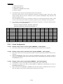
USB interface (with function control functions)
●
Conforms to USB specification, version 2.0 (full speed)
●
Supports a maximum 4 user-defined endpoints.
Transfer type
Endpoint
EP0
EP1
EP2
EP3
EP4
Control
○
-
-
-
-
Bulk
-
○
○
○
○
Interrupt
-
○
○
○
○
Isochronous
Max. payload
-
○
○
○
○
64
64
64
64
64
●
Watchdog timer
● External RC watchdog timer
● Interrupt and reset signals selectable
●
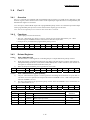
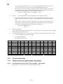
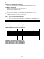
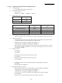
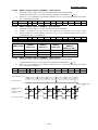
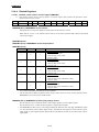
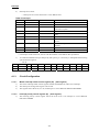
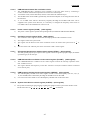
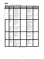
Interrupts
● 28 sources and 10 vectors
1)
Provides three levels (low (L), high (H), and highest (X)) of multiplexed interrupt control. Any
interrupt requests of the level equal to or lower than the current interrupt are not accepted.
2)
When interrupt requests to two or more vector addresses occur at the same time, the interrupt
of the highest level takes precedence over the other interrupts. For interrupts of the same level,
the interrupt into the smallest vector address is honored.
1-3
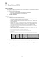
No.
1
Vector
00003H
Level
X or L
INT0
Interrupt Source
2
0000BH
X or L
INT1
3
00013H
H or L
INT2/T0L/INT4/USB bus active/remote control receiver
4
0001BH
H or L
INT3/INT5/base timer
5
00023H
H or L
T0H
6
0002BH
H or L
T1L/T1H
7
00033H
H or L
SIO0/USB bus reset/USB suspend/UART1 receive
8
0003BH
H or L
SIO1/USB endpoint/USB-SOF/SIO4/UART1 transmit
9
00043H
H or L
ADC/T6/T7
10 0004BH
H or L
Port 0/PWM0/PWM1
• Priority levels: X > H > L
• Of interrupts of the same level, the one with the smallest vector address takes precedence.
●
Subroutine stack levels: 1,024 levels maximum (The stack is allocated in RAM.)
●
High-speed multiplication/division instructions
● 16 bits × 8 bits (execution time: 5 Tcyc)
● 24 bits × 16 bits (execution time: 12 Tcyc)
●16 bits÷8 bits (execution time: 8 Tcyc)
●24 bits÷16 bits (execution time: 12 Tcyc)
●
Oscillation circuits and PLL
● RC oscillator circuit (built-in): For system clock
● CF oscillator circuit: For system clock
● Crystal oscillator circuit: For system clock and time-of-day clock
● PLL circuit (built-in): For USB interface
●
Standby function
● HALT mode: Halts instruction execution while allowing the peripheral circuits to
continue operation.
1)
2)
●
HOLD mode: Suspends instruction execution and the operation of the peripheral
circuits.
1)
2)
●
Oscillation will not stop automatically.
Reset by a system reset or interrupt.
The PLL base clock generator, CF oscillator, and RC oscillator automatically stop operation.
There are four ways of releasing the HOLD mode.
(1) Setting the reset pin to the lower level
(2) Setting at least one of the INT0, INT1, INT2, INT4, and INT5 pins to the specified
level
(3) Having an interrupt source established at port 0
(4) Having a bus active interrupt source established in the USB interface circuit
X'tal HOLD mode: Suspends instruction execution and the operation of the
peripheral circuits except the base timer and infrared remote control receiver.
1)
2)
3)
The PLL base clock generator and CF and RC oscillators automatically stop operation.
The state of crystal oscillation established when the hold mode is entered, is retained.
There are six ways of releasing the X'tal HOLD mode.
1-4
LC871A00 Chapter 1
(1) Setting the reset pin to the low level
(2) Setting at least one of the INT0, INT1, INT2, INT4, and INT5 pins to the specified
level
(3) Having an interrupt source established at port 0
(4) Having an interrupt source established in the base timer circuit
(5) Having a bus active interrupt source established in the USB interface circuit
(6) Having an interrupt source established in the infrared remote control receiver circuit
●
Package form
● SQFP48
(lead-free type)
●
Development tools
● On-chip debugger:
TCB87 Type B + LC87F1A32A
1-5
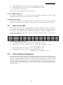
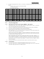
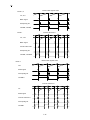
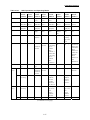
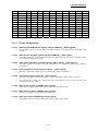
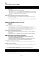
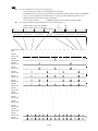
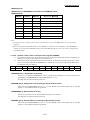
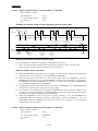
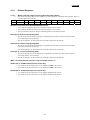
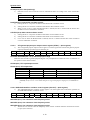
DD+
VDD3
VSS3
P34/UFILT
P33
P32/DBGP2
P31/DBGP1
P30/DBGP0
P70/INT0/T0LCP/AN8/DPUP
P71/INT1/T0HCP/AN9
P72/INT2/T0IN
36
35
34
33
32
31
30
29
28
27
26
25
37
38
39
40
41
42
43
44
45
46
47
48
1
2
3
4
5
6
7
8
9
10
11
12
P27/INT5
P26/INT5
P25/INT5
P24/INT5 /SCK4
P23/INT4/SI4/WR#
P22/INT4/SO4/RD#
P21/INT4/URX1
P20/INT4 /UTX1
P07/AN7/T7O
P06/AN6/T6O
P05/AN5/CKO
P04/AN4
●
P73/INT3/T0IN/RMIN
RES#
XT1/AN10
XT2/AN11
VSS1
CF1
CF2
VDD1
P10/SO0
P11/SI0/SB0
P12/SCK0
P13/SO1
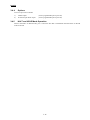
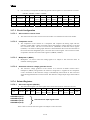
1.3
Pinout
SQFP48
24
23
22
21
20
19
18
17
16
15
14
13
1-6
P03/AN3
P02/AN2
P01/AN1
P00/AN0
VSS2
VDD2
PWM0
PWM1
P17/T1PWMH/BUZ
P16/T1PWML
P15/SCK1
P14/SI1/SB1
LC871A00 Chapter 1
SQFP48
NAME
SQFP48
NAME
1
P73/INT3/T0IN/RMIN
25
P04/AN4
2
RES#
26
P05/AN5/CKO
3
XT1/AN10
27
P06/AN6/T6O
4
XT2/AN11
28
P07/AN7/T7O
5
VSS1
29
P20/INT4/ UTX1
6
CF1
30
P21/INT4/URX1
7
CF2
31
P22/INT4/SO4/RD#
8
VDD1
32
P23/INT4/SI4/WR#
9
P10/SO0
33
P24/INT5/SCK4
10
P11/SI0/SB0
34
P25/INT5
11
P12/SCK0
35
P26/INT5
12
P13/SO1
36
P27/INT5
13
P14/SI1/SB1
37
D-
14
P15/SCK1
38
D+
15
P16/T1PWML
39
VDD3
16
P17/T1PWMH/BUZ
40
VSS3
17
PWM1
41
P34/UFILT
18
PWM0
42
P33
19
VDD2
43
P32/DBGP2
20
VSS2
44
P31/DBGP1
21
P00/AN0
45
P30/DBGP0
22
P01/AN1
46
P70/INT0/T0LCP/AN8/DPUP
23
P02/AN2
47
P71/INT1/T0HCP/AN9
24
P03/AN3
48
P72/INT2/T0IN
1-7
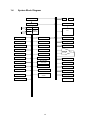
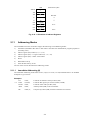
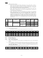
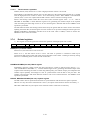
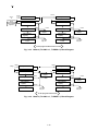
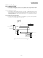
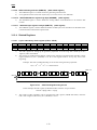
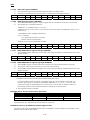
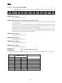
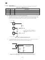
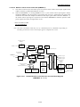
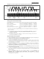
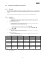
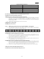
1.4
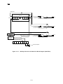
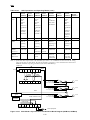
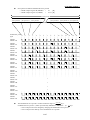
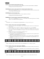
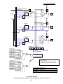
System Block Diagram
IR
Interrupt controller
Standby controller
CF
PLA
FROM
PLL for USB
RC
Clock
X’tal
generator
PC
SIO0
Bus interface
ACC
SIO1
Port 0
B register
SIO4
Port 1
C resister
Timer 0
Port 2
ALU
Timer 1
Port 3
Timer 6
Port 7
Timer 7
INT0 to INT5
Noise filter
Base timer
UART1
PWM0
ADC
Stack pointer
PWM1
Infrared remote
control
Watchdog timer
USB Interface
PSW
RAR
RAM
On-chip debugger
1-8
LC871A00 Chapter 1
1.5
Pin Functions
Pin
VSS1, VSS2,
VSS3
I/O
–
– power supply pin.
Option
No
VDD1, VDD2
–
+ power supply pin
No
VDD3
–
USB reference power supply pin
Yes
• 8-bit I/O port
• I/O specifiable in 4-bit units
• Pull-up resistors can be turned on and off in 4-bit units.
• HOLD release input
• Port 0 interrupt input
• Pin functions
AD converter input port pins: AN0 to AN7 (P00 to P07)
P05: System clock output
P06: Timer 6 toggle output
P07: Timer 7 toggle output
• 8-bit I/O port
• I/O specifiable in 1-bit units
• Pull-up resistors can be turned on and off in 1-bit units.
• Pin functions
P10: SIO0 data output
P11: SIO0 data input/bus I/O
P12: SIO0 clock I/O
P13: SIO1 data output
P14: SIO1 data input/bus I/O
P15: SIO1 clock I/O
P16: Timer 1 PWML output
P17: Timer 1PWMH output/beeper output
• 8-bit I/O port
• I/O specifiable in 1-bit units
• Pull-up resistors can be turned on and off in 1-bit units
• Pin functions
P20-P23: INT4 input/HOLD release input/timer 1 event input
/timer 0L capture input/timer 0H capture input
P24-P27: INT5 input/HOLD release input/timer 1 event input
/timer 0L capture input/timer 0H capture input
P20: UART1 transmit
P21: UART1 receive
P22: SIO4 data I/O/parallel interface RD# output
P23: SIO4 data I/O/parallel interface WR# output
P24: SIO4 clock I/O
Yes
Port 0
P00 to P07
I/O
Port 1
P10 to P17
I/O
Port 2
P20 to P27
I/O
Description
Interrupt acknowledge type
Rising
Falling
Rising &
falling
H level
L level
INT4
Y
Y
Y
N
N
INT5
Y
Y
Y
N
N
(Continued on next page)
1-9
Yes
Yes
Pin Functions (continued)
Pin
Port 3
I/O
I/O
Description
• 5-bit I/O port
• I/O specifiable in 1-bit units.
• Pull-up resistors can be turned on and off in 1-bit units.
• Pin functions
P34: USB interface PLL filter circuit pin
On-chip debugger pins: DBGP0 to DBGP2 (P30 to P32)
I/O
• 4-bit I/O port
• I/O specifiable in 1-bit units
• Pull-up resistors can be turned on and off in 1-bit units.
• Pin functions
P70: INT0 input/HOLD release input/timer 0L capture input
/watchdog timer output/D+ 1.5kΩ pull-up resistor pin
P71: INT1 input/HOLD release input/timer 0H capture input
P72: INT2 input/HOLD release input/timer 0 event input
/timer 0L capture input/high-speed clock counter input
P73: INT3 input (with noise filter)/timer 0 event input
/timer 0H capture input/infrared remote control receiver input
AD converter input port pins: AN8 (P70), AN9 (P71)
P30 to P34
Port 7
P70 to P73
Option
Yes
No
Interrupt acknowledge type
INT0
INT1
INT2
INT3
Rising
Falling
Rising &
falling
H level
L level
Y
Y
Y
Y
Y
Y
Y
Y
N
N
Y
Y
Y
Y
N
N
Y
Y
N
N
PWM0
PWM1
I/O
PWM0, PWM1 output ports
General-purpose input port
No
D−
I/O
USB data I/O pin D−/general-purpose I/O port
No
D+
I/O
USB data I/O pin D+/general-purpose I/O port
No
RES
XT1
Input
Reset pin
No
Input
XT2
I/O
CF1
Input
CF2
• 32.768 kHz crystal oscillator input pin
• Pin functions
General-purpose input port
AD converter input port: AN10
Must be connected to VDD1 if not to be used.
• 32.768 kHz crystal oscillator output pin
• Pin functions
General-purpose input port
AD converter input port: AN11
Must be set to oscillation specification and kept open if not to be
used.
Ceramic oscillator input pin
Output Ceramic oscillator output pin
1-10
No
No
No
No
LC871A00 Chapter 1
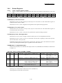
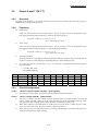
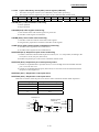
1.6
Port Output Types
The table below lists the types of port outputs and the presence/absence of a pull-up resistor. Data can be
read into an input port even if it is in the output mode.
Port name
P00 to P07
P10 to P17
P20 to P27
P30 to P34
Option
selection
unit
1 bit
1 bit
Option
type
Output type
Pull-up resister
1
CMOS
Programmable (Note 1)
2
N-channel open drain
No
1
CMOS
Programmable
2
N-channel open drain
Programmable
P70
–
No
N-channel open drain
Programmable
P71 to P73
–
No
CMOS
Programmable
PWM0,PWM1
–
No
CMOS
No
D+, D−
–
No
CMOS
No
XT1
–
No
Input only
No
XT2
–
No
Output for 32.768kHz crystal
No
oscillator (N-channel open drain
when in general-purpose output
mode)
Note 1: Programmable pull-up resistors for port 0 are controlled in 4-bit units (P00-P03, P04-P07).
1-11
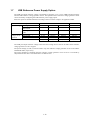
1.7
USB Reference Power Supply Option
The USB port output reference voltage is generated by supplying 4.5 to 5.5V to VDD1 and activating the
internal USB reference voltage generator circuit. The operation of this reference voltage generator circuit
can be selected by configuring the USB reference power supply option.
Select the option as summarized below according to the level of the voltage to be applied to VDD1.
VDD1 voltage (V)
Option setting USB Regulator
USB Regulator in
HOLD mode
USB Regulator in HALT
mode
Reference
Normal operating mode
voltage circuit HOLD mode
operation
HALT mode
Use
Use
4.5 to 5.5
Use
Nonuse
Use
Nonuse
3.0 to 3.6
Nonuse
Nonuse
Use
Nonuse
Use
Nonuse
Active
Active
Active
(1)
Active
Inactive
Inactive
(2)
Active
Inactive
Active
(3)
Inactive
Inactive
Inactive
(4)
The USB port output reference voltage will be the same voltage level as the one at VDD1 if the reference
voltage generator circuit is stopped.
The option settings (2) and (3) must be used to stop the reference voltage generator circuit in the HALT
and HOLD modes, respectively.
The power dissipation consumed when the reference voltage generator circuit is active is increased by
100μA than the one that is consumed when it is held inactive.
1-12
LC871A00 Chapter 2
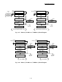
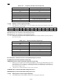
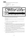
2. Internal Configuration
2.1
Memory Space
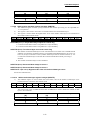
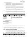
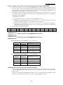
The LC870000 series microcontrollers have the following three types of memory space:
1)
2)
Program memory space:
Internal data memory space:
3)
External data memory space:
256K bytes (128K bytes × 2 banks)
64K bytes (0000H to FDFFH out of 0000H to FFFFH is shared
with the stack area.)
16M bytes
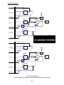
Address
Address
Program memory
space
External data memory
space
FFFFFFH
3FFFFH
Address
ROM bank 1
128KB
Internal data
memory space
FFFFH
RAM
16MB
Reserved for
system
FF00H
FEFFH
SFR (8-bit)
(some 9-bit)
1FFFFH
FE00H
FDFFH
ROM bank 0
128KB
00000H
RAM/Stack
64 KB
(9-bit config.)
0000H
000000H
Note: SFR is the area in which special registers such as the accumulator are allocated (see
Appendixes A-I).
Fig. 2.1.1 Types of Memory Space
2.2
Program Counter (PC)
The program counter (PC) is made up of 17 bits and a bank flag BNK. The value of BNK determines the
bank. The lower-order 17 bits of the PC allows linear access to the 128K ROM space in the current bank.
Normally, the PC advances automatically in the current bank on each execution of an instruction. Bank
switching is accomplished by executing a Return instruction after pushing necessary addresses onto the
stack. When executing a branch or subroutine instruction, when accepting an interrupt, or when a reset is
generated, the value corresponding to each operation is loaded into the PC.
Table 2.2.1 lists the values that are loaded into the PC when the respective operations are performed.
2-1
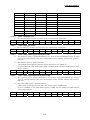
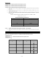
Table 2.2.1 Values Loaded in the PC
Operation
Inter- Reset
rupt
PC value
00000H
BNK value
0
00003H
0
INT1
0000BH
0
INT2/T0L/INT4/USB bus active/Remote controller
reception
00013H
0
INT3/INT5/Base timer
0001BH
0
T0H
00023H
0
T1L/T1H
0002BH
0
SIO0/USB bus reset/UART1 receive
00033H
0
SIO1/USB end point/USB-SOF/SIO4/UART1 transmit
0003BH
0
ADC/T6/T7
00043H
0
Port 0//PWM0/ PWM1
0004BH
0
INT0
Unconditional branch
instructions
JUMP
a17
PC=a17
Unchanged
BR
r12
PC=PC+2+r12[-2048 to +2047]
Unchanged
Conditional branch
instructions
BE, BNE, DBNZ, DBZ, BZ, BNZ,
BZW, BNZW, BP, BN, BPC
PC=PC+nb+r8[-128 to +127]
nb: Number of instruction bytes
Unchanged
Call instructions
CALL
PC=a17
Unchanged
RCALL r12
PC=PC+2+r12[-2048 to +2047]
Unchanged
RCALLA
PC=PC+1+Areg[0 to +255]
Unchanged
Return instructions
RET, RETI
PC16 to 08=(SP)
PC07 to 00=(SP-1)
(SP) denotes the contents of RAM
address designated by the value of
the stack pointer SP.
BNK is set
to bit 8 of
(SP-1).
Standard instructions
NOP, MOV, ADD, …
PC=PC+nb
nb: Number of instruction bytes
Unchanged
2.3
a17
Program Memory (ROM)
The LC870000 series microcontrollers have a program memory space of 256K bytes but the size of the
ROM that is actually incorporated in the microcontroller varies with the CPU type of the microcontroller.
The ROM table lookup instruction (LDC) can be used to reference all ROM data within the bank. Of the
ROM space, the 256 bytes in ROM bank 0 (1FF00H-1FFFFH for ROM sizes of 64K and above and
0FF00H-0FFFFH for ROM sizes of 64K and below) is reserved as the option area. Consequently, this area
is not available as a program area.
2.4
Internal Data Memory (RAM)
The LC870000 series microcontrollers have an internal data memory space of 64K bytes but the size of the
RAM that is actually incorporated in the microcontroller varies with the series of the microcontroller. 9
bits are used to access addresses 0000H to FDFFH of the 128K ROM space and 8 or 9 bits are used to
access addresses FE00H to FFFFH. The 9th bit of RAM is implemented by bit 1 of the PSW and can be
read and written.
The 128 bytes of RAM from 0000H to 007FH are paired to form 64 2-byte and can also be used as 64
indirect address registers. The bit length of these indirect registers is normally 16 bits (8 bits × 2). When
they are used by the ROM table lookup instruction (LDC), however, their bit length is set to 17 bits (9
higher-order bits + 8 lower-order bits).
As shown in Figure 2.4.1, the usable instructions vary depending on the address of RAM.
The efficiency improvement of use ROM and execution speed can be attempted by using these instructions
properly.
2-2
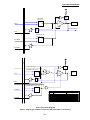
LC871A00 Chapter 2
FFFFH
Reserved for
system
FF00H
FEFFH
SFR space
* 8-bit long
FE00H
FDFFH
2000H
1FFFH
*Note: Some registers are 9-bit long
RAM/
Stack space
9-bit long
0200H
01FFH
0100H
00FFH
0000H
Bit instruction direct (long)
Bit instruction direct (short)
Non-bit instruction direct (long)/indirect, 16-bit operation instruction direct/indirect
Non-bit instruction direct (short)
Fig. 2.4.1 RAM Addressing Map
When the value of the PC is stored in RAM during the execution of a subroutine call instruction or
interrupt, assuming that SP represents the current value of the stack pointer, the value of BNK and the
lower-order 8 bits of the (17-bit) PC are stored in RAM address SP+1 and the higher-order 9 bits in SP+2,
after which SP is set to SP+2.
2.5
Accumulator/A Register (ACC/A)
The accumulator (ACC), also called the A register, is an 8-bit register that is used for data computation,
transfer, and I/O processing. It is allocated to address FE00H in the internal data memory space and
initialized to 00H on a reset.
Address
Initial value
R/W
Name
BIT7
BIT6
BIT5
BIT4
BIT3
BIT2
BIT1
BIT0
FE00
0000 0000
R/W
AREG
AREG7
AREG6
AREG5
AREG4
AREG3
AREG2
AREG1
AREG0
2.6
B Register (B)
The B register is combined with the ACC to form a 16-bit arithmetic register during the execution of a 16bit arithmetic instruction. During a multiplication or division instruction, the B register is used with the
ACC and C register to store the results of computation. In addition, during an external memory access
instruction (LDX or STX), the B register designates the higher-order 8 bits of the 24-bit address.
The B register is allocated to address FE01H of the internal data memory space and initialized to 00H on a
reset.
Address
Initial value
R/W
Name
BIT7
BIT6
BIT5
BIT4
BIT3
BIT2
BIT1
BIT0
FE01
0000 0000
R/W
BREG
BREG7
BREG6
BREG5
BREG4
BREG3
BREG2
BREG1
BREG0
2-3
2.7
C Register (C)
The C register is used with the ACC and B register to store the results of computation during the execution
of a multiplication or division instruction. In addition, during a C register offset indirect instruction, the C
register stores the offset data (-128 to +127) to the contents of an indirect register.
The C register is allocated to address FE02H of the internal data memory space and initialized to 00H on a
reset.
Address
Initial value
R/W
Name
BIT7
BIT6
BIT5
BIT4
BIT3
BIT2
BIT1
BIT0
FE02
0000 0000
R/W
CREG
CREG7
CREG6
CREG5
CREG4
CREG3
CREG2
CREG1
CREG0
2.8
Program Status Word (PSW)
The program status word (PSW) is made up of flags that indicate the status of computation results, a flag
to access the 9th bit of RAM, and a flag to designate the bank during the LDCW instruction. The PSW is
allocated to address FE06H of the internal data memory space and initialized to 00H on a reset.
Address
Initial value
R/W
Name
BIT7
BIT6
BIT5
BIT4
BIT3
BIT2
BIT1
BIT0
FE06
0000 0000
R/W
PSW
CY
AC
PSWB5
PSWB4
LDCBNK
OV
P1
PARITY
CY (bit 7): Carry flag
CY is set (to 1) when a carry occurs as the result of a computation and cleared (to 0) when no carry occurs.
There are the following types of carries:
1)
2)
3)
4)
Carry resulting from an addition
Borrow resulting from a subtraction
Borrow resulting from a comparison
Carry resulting from a rotation
There are some instructions that do not affect this flag at all.
AC (bit 6): Auxiliary carry flag
AC is set (to 1) when a carry or borrow occurs in bit 3 (bit 3 of the higher-order byte during a 16-bit
computation) as the result of an addition or subtraction and cleared (to 0) otherwise.
There are some instructions that do not affect this flag at all.
PSWB5, PSWB4 (bits 5 and 4): User bits
These bits can be read and written through instructions. They can be used by the user freely.
LDCBNK (bit 3): Bank flag for the table lookup instruction (LDCW)
This bit designates the ROM bank to be specified when reading the program ROM with a table lookup
instruction.
(0: ROM-ADR = 0 to 1FFFF, 1: ROM-ADR = 20000 to 3FFFF)
OV (bit 2): Overflow flag
OV is set (to 1) when an overflow occurs as the result of an arithmetic operation and cleared (to 0)
otherwise. An overflow occurs in the following cases:
1)
2)
When MSB is used as the sign bit and when the result of negative number + negative number or
negative number – positive number is a positive number
When MSB is used as the sign bit and when the result of positive number + positive number or
positive number – negative number is a negative number
2-4
LC871A00 Chapter 2
3)
4)
5)
When the higher-order 8 bits of a 16 bits × 8 bits multiplication is nonzero
When the higher-order 16 bits of a 24 bits × 16 bits multiplication is nonzero
When the divisor of a division is 0
There are some instructions that do not affect this flag at all.
P1 (bit 1): RAM bit 8 data flag
P1 is used to manipulate bit 8 of 9-bit internal data RAM (0000H to FDFFH). Its behavior varies
depending on the instruction executed. See Table 2.12.1 for details.
PARITY (bit 0): Parity flag
This bit shows the parity of the accumulator (A register). The parity flag is set (to 1) when there are an odd
number of 1s in the A register. It is cleared (to 0) when there are an even number of 1s in the A register.
2.9
Stack Pointer (SP)
The LC870000 microcontrollers can use RAM addresses 0000H to FDFFH as a stack area. The size of
RAM, however, varies depending on the model of the microcontroller. The SP is 16 bits long and made up
of two registers: SPL (at address FE0A) and SPH (at address FE0B). It is initialized to 0000H on a reset.
The SP is incremented by 1 before data is saved in stack memory and decremented by 1 after the data is
restored from stack memory.
Address
Initial value
R/W
Name
BIT7
BIT6
BIT5
BIT4
BIT3
BIT2
BIT1
BIT0
FE0A
0000 0000
R/W
SPL
SP7
SP6
SP5
SP4
SP3
SP2
SP1
SP0
FE0B
0000 0000
R/W
SPH
SP15
SP14
SP13
SP12
SP11
SP10
SP9
SP8
The value of the SP changes as follows:
1)
2)
3)
4)
2.10
When the PUSH instruction is executed: SP = SP + 1, RAM (SP) = DATA
When the CALL instruction is executed: SP = SP + 1, RAM (SP) = ROMBANK + ADL
SP = SP + 1, RAM (SP) = ADH
When the POP instruction is executed: DATA = RAM (SP), SP = SP - 1
When the RET instruction is executed: ADH = RAM (SP), SP = SP - 1
ROM BANK + ADL = RAM(SP), SP = SP - 1
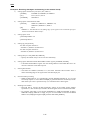
Indirect Addressing Registers
The LC870000 series microcontrollers are provided with three addressing schemes ([Rn], [Rn+C], [off])
that use the contents of indirect registers (indirect addressing modes). (See Section 2.11 for the addressing
modes.) Used for these addressing modes are 64 2-byte indirect registers (R0 to R63) allocated to RAM
addresses 0 to 7EH. The indirect registers can also be used as general-purpose registers (e.g., for saving 2byte data). Naturally, these addresses can be used as ordinary RAM (on a 1 byte (9 bits) basis) if they are
not used as indirect registers. R0 to R63 are "system reserved words" to the assembler and need not be
defined by the user.
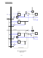
2-5
RAM
Address
Reserved for system
・
7FH
R63 (upper)
7EH
R63 (lower)
03H
R1 (upper)
02H
R1 (lower)
01H
R0 (upper)
00H
R0 (lower)
R63=7EH
R1=2
R0=0
Fig. 2.10.1 Allocation of Indirect Registers
2.11
Addressing Modes
The LC870000 series microcontrollers support the following seven addressing modes:
1)
2)
3)
4)
5)
6)
7)
Immediate (immediate data refers to data whose value has been established at program preparation
(assembly) time.)
Indirect register (Rn) indirect (0 ≦ n ≦ 63)
Indirect register (Rn) + C register indirect (0 ≦ n ≦ 63)
Indirect register (R0) + Offset value indirect
Direct
ROM table look-up
External data memory access
The rest of this section describes these addressing modes.
2.11.1
Immediate Addressing (#)
The immediate addressing mode allows 8-bite (1-byte) or 16-bit (1-word) immediate data to be handled.
Examples are given below.
Examples:
LD
L1: LDW
PUSH
ADD
BE
#12H;
#1234H;
#34H;
#56H;
#78H, L1;
Loads the accumulator with byte data (12H).
Loads the BA register pair with word data (1234H).
Loads the stack with byte data (34H).
Adds byte data (56H) to the accumulator.
Compares byte data (78H) with the accumulator for a branch.
2-6
LC871A00 Chapter 2
2.11.2
Indirect Register Indirect Addressing ([Rn])
In the indirect register indirect addressing mode, it is possible to select one of the indirect registers (R0 to
R63) and use its contents to designate an address in RAM or SFR. When the selected register contains, for
example, "FE02H," it designates the C register.
Example: When R3 contains "123H" (RAM address 6: 23H, RAM address 7: 01H)
LD
[R3];
Transfers the contents of RAM address 123H to the accumulator.
L1: STW
[R3];
Transfers the contents of BA register pair to RAM address 123H.
PUSH [R3];
Saves the contents of RAM address123H in the stack.
SUB
[R3];
Subtracts the contents of RAM address 123H from the accumulator.
DBZ
[R3], L1;
Decrements the contents of RAM address 123H by 1 and causes a branch if
zero.
2.11.3
Indirect Register + C Register Indirect Addressing ([Rn, C])
In the indirect register + C register indirect addressing mode, the result of adding the contents of one of the
indirect registers (R0 to R63) to the contents of the C register (-128 to +127 with MSB being the sign bit)
designates an address in RAM or SFR. For example, if the selected indirect register contains "FE02H" and
the C register contains "FFH (-1)," the address "B register (FE02H + (-1) = FE01H" is designated.
Examples: When R3 contains "123H" and the C register contains "02H"
LD
[R3, C];
Transfers the contents of RAM address 125H to the accumulator.
L1: STW
[R3, C];
Transfers the contents of the BA register pair to RAM address 125H.
PUSH [R3, C];
Saves the contents of 125H in the stack.
SUB
[R3, C];
Subtracts the contents of RAM address 125H from the accumulator.
DBZ
[R3, C], L1; Decrements the contents of RAM address 125H by 1 and causes a branch if
zero.
<Notes on this addressing mode >
The internal data memory space is divided into three closed functional areas as explained in Section 2.1,
namely, 1) system reserved area (FF00 to FFFF), 2) SFR area (FE00 to FEFF), and 3) RAM/stack area
(0000 to FDFF). Consequently, it is disallowed to point to a different area using the value of the C register
from the basic area designated by the contents of Rn. For example, if the instruction "LD [R5,C]" is
executed when R5 contains "0FDFFH" and the C register contains "1," since the basic area is 3)
RAM/stack area (0000 to FDFF), the intended address "0FDFFH+1 = 0FE00H" lies outside the basic area
and "0FFH" as the result of LD is consequently placed in the ACC. If the instruction "LD [R5,C]" is
executed when R5 contains "0FEFFH" and the C register contains "2," since the basic area is 2) SFR area
(FE00 to FEFF), the intended address "0FEFFH+2 = 0FF01H" lies outside the basic area. In this case,
since SFR is confined in an 8-bit address space, the part of the address data addressing outside the 8-bit
address space is ignored and the contents of 0FE01H (B register) are placed in the ACC as the result of the
computation "0FF01H&0FFH+0FE00H = 0FE01."
2-7
2.11.4
Indirect Register (R0) + Offset Value indirect Addressing ([off])
In this addressing mode, the results of adding the 7-bit signed offset data off (-64 to + 63) to the contents
of the indirect register R0 designate an address in RAM or SFR. If R0 contains "FE02H" and off has a
value of "7EH(-2)," for example, the A register (FE02H+(-2) = FE00H) is designated.
Examples: When R0 contains "123H" (RAM address 0: 23H, RAM address 1: 01H)
LD
[10H];
Transfers the contents of RAM address 133H to the accumulator.
L1: STW
[10H];
Transfers the contents of the BA register pair to RAM address 133H.
PUSH [10H];
Saves the contents of RAM address 133H in the stack.
SUB
[10H];
Subtracts the contents of RAM address 133H from the accumulator.
DBZ
[10H], L1;
Decrements the contents of RAM address 133H by 1 and causes a branch if
zero.
<Notes on this addressing mode>
The internal data memory space is divided into three closed functional areas as explained in Section 2.1,
namely, 1) system reserved area (FF00 to FFFF), 2) SFR area (FE00 to FEFF), and 3) RAM/stack area
(0000 to FDFF). Consequently, it is disallowed to point to a different area using an offset value from the
basic area designated by the contents of R0. For example, if the instruction "LD [1]" is executed when R0
contains "0FDFFH," since the basic area is 3) RAM/stack area (0000 to FDFF), the intended address
"0FDFFH+1 = 0FE00H" lies outside the basic area and "0FFH" is placed in the ACC as the results of LD.
If the instruction "LD [2]" is executed when R0 contains "0FEFFH," since the basic area is 2) SFR (FE00
to FEFF), the intended address "0FEFFH+2 = 0FF01H" lies outside the basic area. In this case, since SFR
is confined in an 8-bit address space, the part of the address data addressing outside the 8-bit address space
is ignored and the contents of "0FE01H (B register) are placed in the ACC as the result of computation
"0FF01H&0FFH+0FE00H = 0FE01."
2.11.5
Direct Addressing (dst)
The direct addressing mode allows a RAM or SFR address to be specified directly in an operand. In this
addressing mode, the assembler automatically generates optimum instruction code from the address
specified in the operand (the number of instruction bytes varies according to the address specified in the
operand). Long (middle) range instructions (identified by an "L (M)" at the end of the mnemonic) are
available to make the byte count of instructions constant (align instructions with the longest one).
Examples:
LD
123H;
LDL
123H;
STW
PUSH
SUB
DBZ
123H;
123H;
123H;
123H, L1;
L1:
Transfers the contents of RAM address 123H to the accumulator
(2-byte instruction).
Transfers the contents of RAM address 123H to the accumulator
(3-byte instruction).
Transfers the contents of the BA register pair to RAM address 123H.
Saves the contents of RAM address 123H in the stack.
Subtracts the contents of RAM address 123H from the accumulator.
Decrements the contents of RAM address 123H by 1 and causes a branch if
zero.
2-8
LC871A00 Chapter 2
2.11.6
ROM Table Look-up Addressing
The LC870000 series microcontrollers can read 2-byte data into the BA register pair at once using the
LDCW instruction. Three addressing modes [Rn], [Rn, C], and [off] are available for this purpose. (In this
case only, Rn are configured as 17-bit registers (128K-byte space)).
For models with having bank in ROM, it is possible to reference the ROM data in the ROM bank (128K
bytes) identified by the LDCBNK flag (bit 3) in the PSW. Consequently, when looking into the ROM table
on a series model with banked ROM, execute the LDCW instruction after switching the bank using the
instruction such as SET1 or CLR1 so that the LDCBNK flag designates the ROM bank where the ROM
table resides.
Examples:
TBL: DB
DB
DW
•
•
LDW
CHGP3
CHGP1
STW
LDCW
MOV
LDCW
INC
LDCW
34H
12H
5678H
•
•
#TBL;
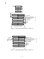
(TBL >> 17) & 1;
(TBL >> 16) & 1;
R0;
[1];
#1, C;
[R0, C];
C;
[R0, C]:
Loads the BA register pair with the TBL address.
Loads LDCBNK in PSW with bit 17 of the TBL address. (Note 1)
Loads P1 in PSW with bit 16 of the TBL address.
Load indirect register R0 with the TBL address (bits 16 to 0).
Reads out the ROM table (B=78H, ACC=12H).
Loads the C register with "01H."
Reads out the ROM table (B=78H, ACC=12H).
Increments the C register by 1.
Reads out the ROM table (B=56H, ACC=78H).
Note 1: LDCBNK (bit 3) of PSW needs to be set up only for models with having bank in ROM.
2.11.7
External Data Memory Addressing
The LC870000 series microcontrollers can access external data memory spaces of up to 16M bytes (24
bits) using the LDX and STX instructions. To designate a 24-bit space, specify the contents of the B
register (8 bits) as the highest-order byte of the address and the contents (16 bits) of (Rn), (Rn) + (C), or
(R0) + off (either one) as the lower-order bytes of the address.
Examples:
LDW
STW
MOV
LDX
#3456H;
R5;
#12H, B;
R5
Sets up the lower-order 16 bits.
Loads the indirect register R5 with the lower-order 16 bits of the address.
Sets up the higher-order 8 bits of the address.
Transfers the contents of external data memory (address 123456H) to the
accumulator.
2-9
2.12
Wait Sequence
2.12.1
Wait Sequence Occurrence
This series of microcontrollers performs wait sequences that suspend the execution of instructions in the
following cases:
1) When continuous data transmission is performed over the SIO0 with SIOCTR (SCON0, bit 4) set, a
wait request is generated ahead of each transfer of 8-bit data, in which case a 1-cycle wait sequence
(RAM data transfer) is performed.
2) When continuous data transmission is performed over the SIO4, a wait request is generated for each
transfer of 8-bit data, in which case a 1-cycle wait sequence (RAM data transfer) is performed.
3) When data packet transmission/reception is performed by the USB interface circuit, a wait request is
generated for each transfer of 4 bytes, in which case a 1-cycle wait sequence (RAM data transfer) is
performed.
2.12.2
1)
2)
3)
4)
5)
What is a Wait Sequence?
When a wait request occurs out of a factor explained in Subsection 2.12.1, the CPU suspends the
execution of the instruction for one cycle, during which transfers the required data. This is called a
wait sequence.
The peripheral circuits such as timers and PWM continue processing during the wait sequence.
A wait sequence extends over no more than two cycles.
The microprocessor performs no wait sequence when it is in the HALT or HOLD mode.
Note that one cycle of discrepancy is introduced between the progresses of the program counter and
time once a wait sequence occurs.
2-10
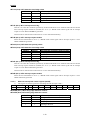
LC871A00 Chapter 2
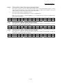
Table 2.12.1
Instruction
LD#/LDW#
LD
LDW
ST
STW
MOV
PUSH#
PUSH
PUSHW
PUSH_P
PUSH_BA
POP
Chart of State Transitions of Bit 8 (RAM / SFR) and P1
BIT8 (RAM/SFR)
P1 (PSW BIT 1)
-
-
-
P1←REG8
-
P1←REGH8
REG8←P1
-
REGL8, REGH8←P1
-
REG8←P1
-
RAM8←P1
-
RAM8←REG8
P1←REG8
RAMH8←REGH8, RAML8←REGL8
P1←REGH8
RAM8←Pl
-
RAMH8←P1, RAML8←P1
-
REG8←RAM8
P1←RAM8
POPW
REGH8←RAMH8, REGL8←RAML8
Pl←RAMH8
POP_P
POP_BA
XCH
XCHW
INC
-
-
REG8↔P1
REGH8←P1, REGL8←Pl, P1←REGH8
INC 9 bits
INCW
INC 17 bits, REGL8←lower byte of CY
DEC
DEC 9 bits
DECW
DBNZ
DEC 17 bits, REGL8← lower byte of CY
inverted
DEC 9 bits
P1←RAMl (bit l)
P1←RAMH8
Same as left.
Same as left.
P1←REG8 after
computation
P1←REGH8 after
computation
P1←REG8 after
computation
P1←REGH8 after
computation
P1←REG8
DBZ
DEC 9 bits
P1←REG8
SET1
NOT1
CLR1
BPC
BP
BN
MUL24
/DIV24
-
-
-
-
-
-
RAM8←1
-
-
-
-
-
-
-
FUNC
-
-
Remarks
P1←bit1 when PSW is
popped
P1←bit1 when higherorder address of PSW is
popped
BIT8 ignored
INC 9 bits
INC 17 bits
DEC 9 bits
DEC 17 bits
DEC 9 bits, check
lower-order 8 bits
DEC 9 bits, check
lower-order 8 bits
Bit 8 of RAM address
for storing results is set
to 1.
Note: A 1 is read if the processing target is an 8-bit register (no bit 8).
Legends:
REG8:
REGH8/REGL8:
RAM8:
RAMH8/RAML8:
Bit 8 of a RAM or SFR location
Bit 8 of the higher-order byte of a RAM location or SFR/bit 8 of the lower-order byte
Bit 8 of a RAM location
Bit 8 of the higher-order byte of a RAM location/bit 8 of the lower-order byte
2-11
2-12
LC871A00 Chapter 3
3. Peripheral System Configuration
This chapter describes the built-in functional blocks (peripheral system) of the LC871A00 series
microcontrollers except the CPU core, RAM, and ROM. Port block diagrams are provided in Appendix A-II
for reference.
3.1
Port 0
3.1.1
Overview
Port 0 is an 8-bit I/O port equipped with programmable pull-up resistors. It is made up of a data latch, a data
direction register, and a control circuit. Control of the input/output signal direction and the pull-up resistors
is accomplished through the data direction register in 4-bit units.
This port can also serve as a terminal for external interrupts and can release the HOLD mode. As a user
option, either CMOS output with a programmable pull-up resistor or N-channel open drain output can be
selected as the output type on a bit basis.
3.1.2
Functions
1)
Input/output port (8 bits: P00-P07)
• The port output data is controlled by port 0 data latch (P0: FE40) on a bit basis.
• I/O control of P00 to P03 is accomplished by P0LDDR (P0DDR: FE41, bit 0).
• I/O control of P04 to P07 is accomplished by P0HDDR (P0DDR: FE41, bit 1).
• Port bits selected as CMOS outputs as user options are provided with programmable
pull-up resistors.
• The programmable pull-up resistors for P00 to P03 are controlled by the P0LPU
(P0DDR: FE41, bit 2).
• The programmable pull-up resistors for P04 to P07 are controlled by P0HPU (P0DDR:
FE41, bit 3).
2)
Interrupt pin function
P0FLG (P0DDR: FE41, bit 5) is set when an input port is specified and 0 level data is input to one of
port bits whose corresponding bit in the port 0 data latch (P0: FE40) is set to 1.
In this case, if P0IE (P0DDR: FE41, bit 4) is 1, the HOLD mode is released and an interrupt request to
vector address 004BH is generated.
3)
Shared pin function
Pin P05 also serves as the system clock output pin, pin P06 as the timer 6 toggle output, and pin P07
as the timer 7 toggle output. Pins P00 to P07 are also used as analog input channel pins AN0 to AN7.
Address
Initial Value
R/W
Name
BIT7
BIT6
BIT5
BIT4
BIT3
BIT2
BIT1
BIT0
FE40
0000 0000
R/W
P0
P07
P06
P05
P04
P03
P02
P01
P00
FE41
HH00 0000
R/W
P0DDR
-
-
P0FLG
P0IE
P0HPU
P0LPU
FE4F
0000 0000
R/W
P0FCRU
T7OE
T6OE
P0HDDR P0LDDR
SCK0SL5 SCK0SL4 CLKOEN CKODV2 CKODV1 CKODV0
3-1
PORTS
3.1.3
Related Registers
3.1.3.1
1)
2)
Port 0 data latch (P0)
The port 0 data latch is an 8-bit register for controlling port 0 output data and port 0 interrupts.
When this register is read with an instruction, data at pins P00 to P07 is read in. If P0 (FE40) is
manipulated with an instruction NOT1, CLR1, SET1, DBZ, DBNZ, INC, or DEC, the contents of
the register are referenced instead of the data at port pins.
Port 0 data can always be read regardless of the I/O state of the port.
3)
Address
Initial Value
R/W
Name
BIT7
BIT6
BIT5
BIT4
BIT3
BIT2
BIT1
BIT0
FE40
0000 0000
R/W
P0
P07
P06
P05
P04
P03
P02
P01
P00
3.1.3.2
1)
Port 0 data direction register (P0DDR)
The port 0 data direction register is a 6-bit register that controls the I/O direction of port 0 data in 4
bit units, the pull-up resistors in 4 bit units, and port 0 interrupts.
Address
Initial Value
R/W
Name
BIT7
BIT6
BIT5
BIT4
BIT3
BIT2
FE41
HH00 0000
R/W
P0DDR
-
-
P0FLG
P0IE
P0HPU
P0LPU
BIT1
BIT0
P0HDDR P0LDDR
P0FLG (bit 5): P0 interrupt source flag
This flag is set when a low level is applied to a port 0 pin that is set up for input and the corresponding P0
(FE40) bit is set.
A HOLD mode release signal and an interrupt request to vector address 004BH are generated when both
this bit and the interrupt request enable bit (P0IE) are set to 1.
This bit must be cleared with an instruction as it is not cleared automatically.
P0IE (bit 4): P0 interrupt request enable
Setting this bit and P0FLG to 1 generates a HOLD mode release signal and an interrupt request to vector
address 004BH
P0HPU (bit 3): P07-P04 pull-up resistor control
When this bit is set to 1 and P0HDDR to 0, pull-up resistors are connected to port bits P07to P04 that are
selected as CMOS output.
P0LPU (bit 2): P03-P00 pull-up resistor control
When this bit is set to 1 and P0LDDR to 0, pull-up resistors are connected to port bits P03 to P00 that are
selected as CMOS output.
P0HDDR (bit 1): P07-P04 I/O control
A 1 in this bit places P07 to P04 into the output mode in which case the contents of the corresponding port 0
data latch (P0) are output.
When this bit is set to 0, P07 to P04 are placed into the input mode and P0FLG is set when a low level is
detected at a port whose corresponding port 0 data latch (P0) bit is set to 1.
P0LDDR (bit 0): P03 to P00 I/O control
A 1 in this bit places P03 to P00 into the output mode in which case the contents of the corresponding port 0
data latch (P0) are output.
When this bit is set to 0, P03 to P00 are placed into the input mode and P0FLG is set when a low level is
detected at a port whose corresponding port 0 data latch (P0) bit is set to 1.
3-2
LC871A00 Chapter 3
3.1.3.3
1)
Port 0 function control register (P0FCRU)
This 6-bit register controls Port 0's shared output pins.
Address
Initial value
R/W
Name
BIT7
BIT6
FE4F
0000 0000
R/W
P0FCRU
T7OE
T6OE
BIT5
BIT4
BIT3
BIT2
BIT1
BIT0
SCKOSL5 SCKOSL4 CLKOEN CKODV2 CKODV1 CKODV0
T7OE (bit 7):
Controls the output data of pin P07. This bit is disabled when P07 is in the input mode.
When P07 is in the output mode:
0: Carries the value of the port data latch.
1: Carries the OR of the waveform that toggles at the interval determined by timer 7 and the value of
the port data latch.
T6OE (bit 6):
Controls the output data of pin P06. This bit is disabled when P06 is in the input mode.
When P06 is in the output mode:
0: Carries the value of the port data latch.
1: Carries the OR of the waveform that toggles at the interval determined by timer 6 and the value of
the port data latch.
SCKOSL5 (bit 5):
SCKOSL4 (bit 4):
These bits are used to select the clock source that is to be sent to P05.
SCKOSL5
0
SCKOSL4
0
P05 Output Clock Source
Source oscillator clock selected as the
system clock
0
1
Internal RC clock
1
0
USB frequency divided clock
1
1
CF clock
CLKOEN (bit 3):
Controls the output data of pin P05. This bit is disabled when P05 is in the input mode.
When P05 is in the output mode:
0: Carries the value of the port data latch.
1: Carries the OR of the system clock output and the value of the port data latch.
CKODV2 (bit 2):
CKODV1 (bit 1):
CKODV0 (bit 0):
Define the frequency of the clock to be placed at P05.
000: Frequency of source oscillator clock to be placed at P05
001: 1/2 of frequency of source clock to be placed at P05
010: 1/4 of frequency of source clock to be placed at P05
011: 1/8 of frequency of source clock to be placed at P05
100: 1/16 of frequency of source clock to be placed at P05
101: 1/32 of frequency of source clock to be placed at P05
110: 1/64 of frequency of source clock to be placed at P05
111: Frequency of source oscillator clock selected as subclock
3-3
PORTS
<Notes on the use of the clock output feature>
Take notes 1) to 4) given below when using the clock output feature. Anomalies may be observed in the
waveform of the port clock output if these notes are violated.
1)
2)
3)
4)
Do not change the frequency of the clock output when CLKOEN (bit 3) is set to 1.
Æ Do not change the settings of CKODV2 to CKODV0 (bits 2 to 0).
Do not change the output clock source selection when CLKOEN (bit 3) is set to 1.
Æ Do not change the settings of SCK0SL5 and SCK0SL4 (bits 5 and 4).
Do not change the system clock selection when CLKOEN (bit 3) is set to 1.
Æ Do not change the settings of CLKCB5 and CLKCB4 (bits 5 and 4) of the OCR register.
CLKOEN will not go to 0 immediately even when the user executes an instruction that loads the
P0FCRU register with such data that sets the state of CLKOEN from 1 to 0. CLKOEN is set to 0 at
the end of the clock that is being output (on detection of a falling edge of the clock). Accordingly,
when changing the clock divider setting or changing the system clock selection after setting
CLKOEN to 0 with an instruction, be sure to read the CLKOEN value in advance and make sure
that it is 0.
DVCKON
CLKCB5, 4
2
Selector
Selector
UDVSEL2, 1, 0
SCK0SL5, 4
Source oscillator
clock selected as
system clock
CKODV2, 1, 0
2
3
USB freq. divided clock
Subclock
Subclock
oscillator
Figure 3.1.1 P05 Output Clock Selector Circuit
3.1.4
Options
Two user options are available.
1)
2)
CMOS output (with a programmable pull-up resistor)
N-channel open drain output
3-4
Selector
RC clock
RC oscillator
Freq. divider
CF clock
CF oscillator
Selector
48MHz
Freq.
divider
PLL oscillator
3
To P05
LC871A00 Chapter 3
3.1.5
HALT and HOLD Mode Operation
When in the HALT or HOLD mode, port 0 retains the state that is established when the HALT or HOLD
mode is entered.
3-5
PORTS
3.2
Port 1
3.2.1
Overview
Port 1 is an 8-bit I/O port equipped with programmable pull-up resistors. It is made up of a data latch, a data
direction register, a function control register, and a control circuit. Control of the input/output signal
direction is accomplished by the data direction register on a bit basis. Port 1 can also be used as a serial
interface I/O port or PWM output port by manipulating its function control register.
As a user option, either CMOS output with a programmable pull-up resistor or N-channel open drain output
can be selected as the output type on a bit basis.
3.2.2
1)
2)
Functions
I/O port (8 bits: P10 to P17)
• The port output data is controlled by the port 1 data latch (P1: FE44) and the I/O
direction is controlled by the port 1 data direction register (P1DDR: FE45).
• Each port bit is provided with a programmable pull-up resistor.
Shared functions
P17 is also used as the timer 1 PWMH / base timer BUZ output, P16 as the timer 1 PWML
output, P15 to P13 as SIO1 I/O, and P12 to P10 as SIO0 I/O.
Address
Initial Value
R/W
Name
BIT7
BIT6
BIT5
BIT4
BIT3
BIT2
BIT1
BIT0
FE44
0000 0000
R/W
P1
P17
P16
P15
P14
P13
P12
P11
P10
FE45
0000 0000
R/W
P1DDR
P17DDR P16DDR P15DDR P14DDR P13DDR P12DDR P11DDR P10DDR
FE46
0000 0000
R/W
P1FCR
P17FCR
P16FCR
P15FCR
P14FCR
P13FCR
P12FCR
P11FCR
P10FCR
3.2.3
Related Registers
3.2.3.1
1)
2)
Port 1 data latch (P1)
The port 1 data latch is an 8-bit register for controlling port 1 output data and pull-up resistors.
When this register is read with an instruction, data at pins P10 to P17 is read in. If P1 (FE44) is
manipulated with an instruction NOT1, CLR1, SET1, DBZ, DBNZ, INC, or DEC, the contents of
the register are referenced instead of the data at port pins.
Port 1 data can always be read regardless of the I/O state of the port.
3)
Address
Initial Value
R/W
Name
BIT7
BIT6
BIT5
BIT4
BIT3
BIT2
BIT1
BIT0
FE44
0000 0000
R/W
P1
P17
P16
P15
P14
P13
P12
P11
P10
3-6
LC871A00 Chapter 3
3.2.3.2
1)
2)
Port 1 data direction register (P1DDR)
The port 1 data direction register is an 8-bit register that controls the I/O direction of port 1 data on a
bit basis. Port P1n are placed in the output mode when bit P1nDDR is set to 1 and in the input mode
when bit P1nDDR is set to 0.
When bit P1nDDR is set to 0 and the bit P1n of the port 1 data latch is set to 1, port P1n becomes an
input with a pull-up resistor.
Address
Initial Value
R/W
Name
FE45
0000 0000
R/W
P1DDR
Register Data
P1n
P1nDDR
0
0
BIT7
BIT6
BIT5
BIT4
BIT3
BIT2
BIT1
BIT0
P17DDR P16DDR P15DDR P14DDR P13DDR P12DDR P11DDR P10DDR
Port P1n State
Output
Built-in Pull-up
Resistor
Input
Enabled
Open
OFF
1
0
Enabled
Built-in pull-up resistor
ON
0
1
Enabled
Low
OFF
1
1
Enabled
High/open (CMOS/N-channel open drain)
OFF
3.2.3.3
1)
Port 1 function control register (P1FCR)
The port 1 function control register is an 8-bit register that controls the shared functions of port 1.
Address
Initial Value
R/W
Name
BIT7
BIT6
BIT5
BIT4
BIT3
BIT2
BIT1
BIT0
FE46
0000 0000
R/W
P1FCR
P17FCR
P16FCR
P15FCR
P14FCR
P13FCR
P12FCR
P11FCR
P10FCR
n
7
6
5
4
3
2
1
0
P1nFCR
0
P1n
–
P1n Pin Data in Output Mode (P1nDDR=1)
Value of port data latch (P17)
1
0
AND of timer 1 PWMH and base timer BUZ
1
1
NAND of timer 1 PWMH and base timer BUZ
0
–
Value of port data latch (P16)
1
0
Timer 1 PWML data
1
1
Inverted data of timer 1 PWML data
0
–
Value of port data latch (P15)
1
0
SIO1 clock output data
1
1
High output
0
–
Value of port data latch (P14)
1
0
SIO1 output data
1
1
High output
0
–
Value of port data latch (P13)
1
0
SIO1 output data
1
1
High output
0
–
Value of port data latch (P12)
1
0
SIO0 clock output data
1
1
High output
0
–
Value of port data latch (P11)
1
0
SIO0 output data
1
1
High output
0
–
Value of port data latch (P10)
1
0
SIO0 output data
1
1
High output
The high data output at a pin that is selected as an N-channel open drain output (user option) is represented
by an open circuit.
3-7
PORTS
P17FCR (bit 7): P17 function control (timer 1 PWMH & base timer BUZ output control)
This bit controls the output data at pin P17.
When P17 is placed in the output mode (P17DDR=1) and P17FCR is set to 1, the AND of timer 1 PWMH
output and BUS output from the base timer is EORed with the port data latch and the result is placed at pin
17.
P16FCR (bit 6): P16 function control (timer 1 PWML output control)
This bit controls the output data at pin P16.
When P16 is placed in the output mode (P16DDR=1) and P16FCR is set to 1, the EOR of timer 1 PWML
output data and the port data latch is placed at pin 16.
P15FCR (bit 5): P15 function control (SIO1 clock output control)
This bit controls the output data at pin P15.
When P15 is placed in the output mode (P15DDR=1) and P15FCR is set to 1, the OR of the SIO1 clock
output data and the port data latch is placed at pin 15.
P14FCR (bit 4): P14 function control (SIO1 data output control)
This bit controls the output data at pin P14.
When P14 is placed in the output mode (P14DDR=1) and P14FCR is set to 1, the OR of the SIO1 output
data and the port data latch is placed at pin P14.
When the SIO1 is active, SIO1 input data is read from P14 regardless of the I/O state of P14.
P13FCR (bit 3): P13 function control (SIO1 data output control)
This bit controls the output data at pin P13.
When P13 is placed in the output mode (P13DDR=1) and P13FCR is set to 1, the OR of the SIO1 output
data and the port data latch is placed at pin P13.
P12FCR (bit 2): P12 function control (SIO0 clock output control)
This bit controls the output data at pin P12.
When P12 is placed in the output mode (P12DDR=1) and P12FCR is set to 1, the OR of the SIO0 clock
output data and the port data latch is placed at pin P12.
P11FCR (bit 1): P11 function control (SIO0 data output control)
This bit controls the output data at pin P11.
When P11 is placed in the output mode (P11DDR=1) and P11FCR is set to 1, the OR of the SIO0 output
data and the port data latch is placed at pin P11.
When the SIO0 is active, SIO0 input data is read from P11 regardless of the I/O state of P11.
P10FCR (bit 0): P10 function control (SIO0 data output control)
This bit controls the output data at pin P10.
When P10 is placed in the output mode (P10DDR=1) and P10FCR is set to 1, the OR of the SIO0 output
data and the port data latch is placed at pin P10.
3-8
LC871A00 Chapter 3
3.2.4
Options
Two user options are available.
1)
2)
3.2.5
CMOS output
N-channel open drain output
(with a programmable pull-up resistor)
(with a programmable pull-up resistor)
HALT and HOLD Mode Operation
When in the HALT or HOLD mode, port 1 retains the state that is established when the HALT or HOLD
mode is entered.
3-9
PORTS
3.3
Port 2
3.3.1
Overview
Port 2 is an 8-bit I/O port equipped with programmable pull-up resistors. It is made up of a data latch, a data
direction register, and a control circuit. Control of the input/output signal direction is accomplished by the
data direction register on a bit basis.
Port 2 can also serve as an input port for external interrupts. It can also be used as an input port for the timer
1 count clock input, timer 0 capture signal input, and HOLD mode release signal input.
As a user option, either CMOS output with a programmable pull-up resistor or N-channel open drain output
with a programmable pull-up resistor can be selected as the output type on a bit basis.
3.3.2
1)
2)
3)
Functions
Input/output port (8 bits: P20 to P27)
• The port 2 data latch (P2: FE48) is used to control port output data and the port 2 data
direction register (P2DDR: FE49) to control the I/O direction of port data.
• Each port bit is provided with a programmable pull-up resistor.
Interrupt input pin function
• The port (INT4) selected out of P20 to P23 and the port (INT5) selected out of P24 to
P27 are provided with a pin interrupt function. This function senses a low edge, a high
edge, or both edges and sets the interrupt flag. These two selected ports can also serve as
timer 1 counter clock input and timer 0 capture signal input.
Hold mode release function
• When the interrupt flag and interrupt enable flag are set by INT4 or INT5, a HOLD
mode release signal is generated, releasing the HOLD mode. The CPU then enters the
HALT mode (main oscillation by CR). When the interrupt is accepted, the CPU switches
from the HALT mode to normal operating mode.
• When a signal change, such that the interrupt flag is set, is input to INT4 or INT5 in the
HOLD mode, the interrupt flag is set. In this case, the HOLD mode is released if the
corresponding interrupt enable flag is set.
The interrupt flag, however, cannot be set by a rising edge occurring when INT4 or INT5
data which is established when the HOLD mode is entered, is in the high state or by a
falling edge occurring when INT4 or INT5 data which is established when the HOLD
mode is entered, is in the low state. Consequently, to release the HOLD mode with INT4
or INT5, it is recommended that INT4 or INT5 be used in the double edge interrupt
mode.
3-10
LC871A00 Chapter 3
Address Initial Value
R/W
Name
BIT7
BIT6
BIT5
BIT4
BIT3
BIT2
BIT1
BIT0
FE48
0000 0000
R/W
P2
P27
P26
P25
P24
P23
P22
P21
P20
FE49
0000 0000
R/W
P2DDR
P27DDR
P26DDR
P25DDR
P24DDR
P23DDR
P22DDR
P21DDR
P20DDR
FE4A
0000 0000
R/W
145CR
INT5HEG INT5LEG
INT5IF
INT5IE
INT4HEG INT4LEG
INT4IF
INT4IE
FE4B
0000 0000
R/W
145SL
15SL1
15SL0
14SL1
14SL0
15SL3
15SL2
14SL3
14SL2
3.3.3
Related Registers
3.3.3.1
1)
2)
Port 2 data latch (P2)
The port 2 data latch is an 8-bit register for controlling port 2 output data and pull-up resistors.
When this register is read with an instruction, data at pins P20 to P27 is read in. If P2 (FE48) is
manipulated with an instruction NOT1, CLR1, SET1, DBZ, DBNZ, INC, or DEC, the contents of
the register are referenced instead of the data at port pins.
Port 2 data can always be read regardless of the I/O state of the port.
3)
Address
Initial Value
R/W
Name
BIT7
BIT6
BIT5
BIT4
BIT3
BIT2
BIT1
BIT0
FE48
0000 0000
R/W
P2
P27
P26
P25
P24
P23
P22
P21
P20
3.3.3.2
1)
2)
Port 2 data direction register (P2DDR)
The port 2 data direction register is an 8-bit register that controls the I/O direction of port 2 data on a
bit basis. Port P2n are placed in the output mode when bit P2nDDR is set to 1 and in the input mode
when bit P2nDDR is set to 0.
When bit P2nDDR is set to 0 and the bit P2n of the port 2 data latch is set to 1, port P2n becomes an
input with a pull-up resistor
Address
Initial Value
R/W
Name
FE49
0000 0000
R/W
P2DDR
Register Data
P2n
P2nDDR
0
0
BIT7
BIT6
BIT5
BIT4
BIT3
BIT2
BIT1
BIT0
P27DDR P26DDR P25DDR P24DDR P23DDR P22DDR P21DDR P20DDR
Port P2n State
Output
Built-in Pull-up
Resistor
Input
Enabled
Open
OFF
1
0
Enabled
Built-in pull-up resistor
ON
0
1
Enabled
Low
OFF
1
1
Enabled
High/open (CMOS/N-channel open drain)
OFF
3.3.3.3
1)
External interrupt 4/5 control register (I45CR)
This register is an 8-bit register for controlling external interrupts 4 and 5.
Address Initial Value R/W
FE4A
0000 0000
R/W
Name
I45CR
BIT7
BIT6
INT5HEG INT5LEG
BIT5
BIT4
INT5IF
INT5IE
BIT3
BIT2
INT4HEG INT4LEG
INT5HEG (bit 7): INT5 rising edge detection control
INT5LEG (bit 6): INT5 falling edge detection control
INT5HEG
0
INT5LEG
0
INT5 Interrupt Conditions (Pin Data)
No edge detection
0
1
Falling edge detection
1
0
Rising edge detection
1
1
Both edges detection
3-11
BIT1
BIT0
INT4IF
INT4IE
PORTS
INT5IF (bit 5): INT5 interrupt source flag
This bit is set when the conditions specified by INT5HEG and INT5LEG are satisfied.
When this bit and the INT5 interrupt request enable bit (INT5IE) are set to 1, a HOLD mode release signal
and an interrupt request to vector address 001BH are generated.
The interrupt flag, however, cannot be set by a rising edge occurring when INT5 data which is established
when the HOLD mode is entered is in the high state or by a falling edge occurring when INT5 data which is
established when the HOLD mode is entered is in the low state. Consequently, to release the HOLD mode
with INT5, it is recommended that INT5 be used in the double edge interrupt mode.
This bit must be cleared with an instruction as it is not cleared automatically.
INT5IE (bit 4): INT5 interrupt request enable
When this bit and INT5IF are set to 1, a HOLD mode release signal and an interrupt request to vector
address 001BH are generated.
INT4HEG (bit 3): INT4 rising edge detection control
INT4LEG (bit 2): INT4 falling edge detection control
INT4HEG
0
INT4LEG
0
INT4 Interrupt Conditions (Pin Data)
No edge detection
0
1
Falling edge detection
1
0
Rising edge detection
1
1
Both edges detection
INT4IF (bit 1): INT4 interrupt source flag
This bit is set when the conditions specified by INT4HEG and INT4LEG are satisfied.
When this bit and the INT4 interrupt request enable bit (INT4IE) are set to 1, a HOLD mode release signal
and an interrupt request to vector address 0013H are generated.
The interrupt flag, however, cannot be set by a rising edge occurring when INT4 data which is established
when the HOLD mode is entered is in the high state or by a falling edge occurring when INT4 data which is
established when the HOLD mode is entered is in the low state. Consequently, to release the HOLD mode
with INT4, it is recommended that INT4 be used in the double edge interrupt mode.
This bit must be cleared with an instruction as it is not cleared automatically.
INT4IE (bit 0): INT4 interrupt request enable
When this bit and INT4IF are set to 1, a HOLD mode release signal and an interrupt request to vector
address 0013H are generated.
3.3.3.4
1)
External interrupt 4/5 pin select register (I45SL)
This register is an 8-bit register used to select pins for the external interrupts 4 and 5.
Address
Initial Value
R/W
Name
BIT7
BIT6
BIT5
BIT4
BIT3
BIT2
BIT1
BIT0
FE4B
0000 0000
R/W
I45SL
15SL3
15SL2
15SL1
15SL0
14SL3
14SL2
14SL1
14SL0
3-12
LC871A00 Chapter 3
I5SL3 (bit 7): INT5 pin select
I5SL2 (bit 6): INT5 pin select
I5SL3
0
I5SL2
0
Pin Assigned to INT5
Port P24
0
1
Port P25
1
0
Port P26
1
1
Port P27
I5SL1 (bit 5): INT5 pin function select
I5SL0 (bit 4): INT5 pin function select
When the data change specified in the external interrupt 4/5 control register (I45CR) is given to the pin that
is assigned to INT5, timer 1 count clock input and timer 0 capture signal are generated.
I5SL1
0
I5SL0
0
Function other than INT5 Interrupt
None
0
1
Timer 1 count clock input
1
0
Timer 0L capture signal input
1
1
Timer 0H capture signal input
I4SL3 (bit 3): INT4 pin select
I4SL2 (bit 2): INT4 pin select
I4SL3
0
I4SL2
0
Pin Assigned to INT4
Port P20
0
1
Port P21
1
0
Port P22
1
1
Port P23
I4SL1 (bit 1): INT4 pin function select
I4SL0 (bit 0): INT4 pin function select
When the data change specified in the external interrupt 4/5 control register (I45CR) is given to the pin that
is assigned to INT4, timer 1 count clock input and timer 0 capture signal are generated.
Notes:
1)
2)
3)
I4SL1
0
I4SL0
0
Function other than INT4 Interrupt
None
0
1
Timer 1 count clock input
1
0
Timer 0L capture signal input
1
1
Timer 0H capture signal input
When timer 0L capture signal input or timer 0H capture signal input is specified for INT4 or
INT5 together with port 7, the signal from port 7 is ignored.
When INT4 and INT5 are specified in duplicate for timer 1 count clock input, timer 0L capture
signal input, or timer 0H capture signal input, both interrupts are accepted. If both INT4 and
INT5 events occur at the same time, however, only one event is recognized.
When at least one of INT4 and INT5 is specified as timer 1 count clock input, timer 1L
functions as an event counter. If neither INT4 nor INT5 are specified for timer 1 count clock
input, the timer 1L counter counts on every 2Tcyc.
3-13
PORTS
3.3.4
Options
Two user options are available.
1)
2)
3.3.5
CMOS output
N-channel open drain output
(with a programmable pull-up resistor)
(with a programmable pull-up resistor)
HALT and HOLD Mode Operation
When in the HALT or HOLD mode, port 2 retains the state that is established when the HALT or HOLD
mode is entered.
3-14
LC871A00 Chapter 3
3.4
Port 3
3.4.1
Overview
Port 3 is a 5-bit I/O port equipped with programmable pull-up resistors. It is made up of a data latch, a data
direction register, and a control circuit. Control of the input/output signal direction is accomplished by the
data direction register on a bit basis.
As a user option, either CMOS output with a programmable pull-up resistor or N-channel open drain output
with a programmable pull-up resistor can be selected as the output type on a bit basis.
Note: Port 30 is temporally set low when the microcontroller is released.
3.4.2
1)
Functions
Input/output port (5 bits: P30 to P34)
• The port 3 data latch (P3: FE4C) is used to control the port output data and the port 3 data
direction register (P3DDR: FE4D) to control the I/O direction of port data.
• Each port bit is provided with a programmable pull-up resistor.
Address
Initial Value
R/W
Name
BIT7
BIT6
BIT5
BIT4
BIT3
BIT2
BIT1
BIT0
FE4C
HHH0 0000
R/W
P3
-
-
-
P34
P33
P32
P31
P30
FE4D
HHH0 0000
R/W
P3DDR
-
-
-
P34DDR P33DDR P32DDR P31DDR P30DDR
3.4.3
Related Registers
3.4.3.1
1)
2)
Port 3 data latch (P3)
This data latch is a 5-bit register for controlling the port 3 output data and its pull-up resistors.
When this register is read with an instruction, the data at pins P30 to P34 is read in. If P3 (FE4C) is
manipulated using the NOT1, CLR1, SET1, DBZ, DBNZ, INC or DEC instruction, the contents of
the register is referenced instead of the data at the pins.
Data can always be read from port 3 regardless of its I/O state.
3)
Address
Initial Value
R/W
Name
BIT7
BIT6
BIT5
BIT4
BIT3
BIT2
BIT1
BIT0
FE4C
HHH0 0000
R/W
P3
-
-
-
P34
P33
P32
P31
P30
3.4.3.2
1)
2)
Port 3 data direction register (P3DDR)
The port 3 data direction register is a 5-bit register for controlling the I/O direction of 3 port data on
a bit basis. Port P3n is placed in the output mode when bit P3nDDR is set to 1 and in the input mode
when bit P3nDDR is set to 0.
Port P3n is designated as an input with a pull-up resistor when bit P3nDDR is set to 0 and bit P3n of
port 3 data latch is set to 1.
Address
Initial Value
R/W
Name
BIT7
BIT6
BIT5
FE4D
HHH0 0000
R/W
P3DDR
-
-
-
Register Data
P3n
P3nDDR
0
0
BIT4
BIT3
BIT2
BIT1
Port P3n State
Output
Built-in Pull-up
Resistor
Input
Enabled
Open
OFF
1
0
Enabled
Built-in pull-up resistor
ON
0
1
Enabled
Low
OFF
1
1
Enabled
High/open (CMOS/N-channel open drain)
OFF
3-15
BIT0
P34DDR P33DDR P32DDR P31DDR P30DDR
PORTS
3.4.4
Options
Two user options are available.
1)
2)
3.4.5
CMOS output
N-channel open drain output
(with a programmable pull-up resistor)
(with a programmable pull-up resistor)
HALT and HOLD Mode Operation
When in the HALT or HOLD mode, port 3 retains the state that is established when the HALT or HOLD
mode is entered.
3-16
LC871A00 Chapter 3
3.5
Port 7
3.5.1
Overview
Port 7 is a 4-bit I/O port equipped with programmable pull-up resistors. It is made up of a data control latch
and a control circuit. The input/output direction of port data can be controlled on a bit basis.
Port 7 can be used as an input port for external interrupts. It can also be used as an input port for the timer 0
count clock input, capture signal input, and HOLD mode release signal input.
There is no user option for this port.
3.5.2
1)
2)
3)
Functions
Input/output port (4 bits: P70 to P73)
• The lower-order 4 bits of the port 7 control register (P7: FE5C) are used to control the
port output data and the higher-order 4 bits to control the I/O direction of port data.
• P70 is of the N-channel open drain output type and P71 to P73 are of CMOS output type.
• Each port bit is provided with a programmable pull-up resistor.
Interrupt input pin function
• P70 and P71 are assigned to INT0 and INT1, respectively, and used to detect a low or
high level, or a low or high edge and set the interrupt flag.
• P72 and P73 are assigned to INT2 and INT3, respectively, and used to detect a low or
high edge, or both edges and set the interrupt flag.
Timer 0 count input function
A count signal is sent to timer 0 each time a signal change such that the interrupt flag is set is supplied
to the port selected from P72 and P73.
4)
Timer 0L capture input function
A timer 0L capture signal is generated each time a signal change such that the interrupt flag is set is
supplied to the port selected from P70 and P72.
When a selected level of signal is input to P70 that is specified for level-triggered interrupts, a timer
0L capture signal is generated at 1 cycle interval for the duration of the signal.
5)
Timer 0H capture input function
A timer 0H capture signal is generated each time a signal change such that the interrupt flag is set is
supplied to the port selected from P71 and P73.
When a selected level of signal is input to P71 that is specified for level-triggered interrupts, a timer
0H capture signal is generated at 1 cycle interval for the duration of the signal.
3-17
PORTS
6)
HOLD mode release function
• When the interrupt flag and interrupt enable flag are set by INT0, INT1, or INT2, a
HOLD mode release signal is generated, releasing the HOLD mode. The CPU then
enters the HALT mode (main oscillation by CR). When the interrupt is accepted, the
CPU switches from the HALT mode to normal operating mode.
• When a signal change such that the interrupt flag is set is input to P70 or P71 in the
HOLD mode, the interrupt flag is set. In this case, the HOLD mode is released if the
corresponding interrupt enable flag is set.
• When a signal change such that the interrupt flag is set is input to P72 in the HOLD
mode, the interrupt flag is set. In this case, the HOLD mode is released if the
corresponding interrupt enable flag is set. The interrupt flag, however, cannot be set by a
rising edge occurring when P72 data which is established when the HOLD mode is
entered, is in the high state or by a falling edge occurring when P72 data which is
established when the HOLD mode is entered, is in the low state. Consequently, to release
the HOLD mode with P72, it is recommended that P72 be used in the double edge
interrupt mode.
Timer 0
Count
Input
-
Timer 0L
Enabled
-
Timer 0H
Enabled
L edge, H edge,
Available
Timer 0L
both
edges
P73
Available
Timer 0H
Note: P70 and P71 HOLD mode release is available only when level detection is set.
Enabled
P70
P71
P72
7)
Interrupt Input
Signal Detection
Input
Output
With
programmable
pull-up
resistor
N-channel open drain
CMOS
L level, H level,
L edge, H edge
Capture Hold Mode
Input
Release
-
Analog voltage input function
• P70 and P71 are used to receive the analog voltage inputs to the AD converter.
Address Initial Value R/W
Name
BIT7
BIT6
BIT5
BIT4
BIT3
BIT2
BIT1
BIT0
FE5C
0000 0000
R/W
P7
P73DDR
P72DDR
P71DDR
P70DDR
P73DT
P72DT
P71DT
P70DT
FE5D
0000 0000
R/W
I01CR
INT1LH
INT1LV
INT1IF
INT1IE
INT0LH
INT0LV
INT0IF
INT0IE
FE5E
0000 0000
R/W
I23CR
INT2IF
INT2IE
FE5F
0000 0000
R/W
ISL
NFON
ST0IN
INT3HEG INT3LEG
ST0HCP
ST0LCP
INT3IF
INT3IE
BTIMC1
BTIMC0
INT2HEG INT2LEG
BUZON
NFSEL
3.5.3
Related Registers
3.5.3.1
1)
Port 7 control register (P7)
The port 7 control register is an 8-bit register for controlling the I/O of port 7 data and pull-up
resistors.
When this register is read with an instruction, data at pins P70 to P73 is read into bits 0 to 3. Bits 4
to 7 are loaded with bits 4 to 7 of register P7. If P7 (FE5C) is manipulated with an instruction NOT1,
CLR1, SET1, DBZ, DBNZ, INC, or DEC, the contents of the register are referenced as bits 0 to 3
instead of the data at port pins.
Port 7 data can always be read regardless of the I/O state of the port
2)
3)
Address
Initial Value
R/W
Name
FE5C
0000 0000
R/W
P7
BIT7
BIT6
BIT5
BIT4
P73DDR P72DDR P71DDR P70DDR
3-18
BIT3
BIT2
BIT1
BIT0
P73DT
P72DT
P71DT
P70DT
LC871A00 Chapter 3
Register Data
P7n
P7nDDR
0
0
Input
Enabled
Port P7n State
Output
Open
Built-in Pull-up Resistor
OFF
1
0
Enabled
Built-in pull-up resistor
ON
0
1
Enabled
CMOS-Low
OFF
1
1
Enabled
CMOS-High (P70 is open)
ON
P73DDR (bit 7): P73 I/O control
A 1 or 0 in this bit controls the output (CMOS) or input of pin P73.
P72DDR (bit 6): P72 I/O control
A 1 or 0 in this bit controls the output (CMOS) or input of pin P72.
P71DDR (bit 5): P71 I/O control
A 1 or 0 in this bit controls the output (CMOS) or input of pin P71.
P70DDR (bit 4): P70 I/O control
A 1 or 0 in this bit controls the output (N-channel open drain) or input of pin P70.
P73DT (bit 3): P73 data
The value of this bit is output from pin P73 when P73DDR is set to 1.
A 1 or 0 in this bit turns on and off the built-in pull-up resistor for pin P73.
P72DT (bit 2): P72 data
The value of this bit is output from pin P72 when P72DDR is set to 1.
A 1 or 0 in this bit turns on and off the built-in pull-up resistor for pin P72.
P71DT (bit 1): P71 data
The value of this bit is output from pin P71 when P71DDR is set to 1.
A 1 or 0 in this bit turns on and off the built-in pull-up resistor for pin P71.
P70DT (bit 0): P70 data
The value of this bit is output from pin P70 when P70DDR is set to 1. Since this bit is of N-channel open
drain output type, however, it is placed in the high-impedance state when P70DT is set to 1.
A 1 or 0 in this bit turns on and off the built-in pull-up resistor for pin P70.
3.5.3.2
1)
External interrupt 0/1 control register (I01CR)
This register is an 8-bit register for controlling external interrupts 0 and 1.
Address
Initial Value
R/W
Name
BIT7
BIT6
BIT5
BIT4
BIT3
BIT2
BIT1
BIT0
FE5D
0000 0000
R/W
I01CR
INT1LH
INT1LV
INT1IF
INT1IE
INT0LH
INT0LV
INT0IF
INT0IE
INT1LH (bit 7): INT1 detection polarity select
3-19
PORTS
INT1LV (bit 6): INT1 detection level/edge select
INT1LH
0
INT1LV
0
INT1 Interrupt Conditions (P71 Pin Data)
Falling edge detection
0
1
Low level detection
1
0
Rising edge detection
1
1
High level detection
INT1IF (bit 5): INT1 interrupt source flag
This bit is set when the conditions specified by INT1LH and INT1LV are satisfied. When this bit and the
INT1 interrupt request enable bit (INT1IE) are set to 1, a HOLD mode release signal and an interrupt
request to vector address 000BH are generated.
This bit must be cleared with an instruction as it is not cleared automatically.
INT1IE (bit 4): INT1 interrupt request enable
When this bit and INT1IF are set to 1, a HOLD mode release signal and an interrupt request to vector
address 000BH are generated.
INT0LH (bit 3): INT0 detection polarity select
INT0LV (bit 2): INT0 detection level/edge select
INT0LH
0
INT0LV
0
INT0 Interrupt Conditions (P70 Pin Data)
Falling edge detection
0
1
Low level detection
1
0
Rising edge detection
1
1
High level detection
INT0IF (bit 1): INT0 interrupt source flag
This bit is set when the conditions specified by INT0LH and INT0LV are satisfied. When this bit and the
INT0 interrupt request enable bit (INT0IE) are set to 1, a HOLD mode release signal and an interrupt
request to vector address 0003H are generated.
This bit must be cleared with an instruction as it is not cleared automatically.
INT0IE (bit 0): INT0 interrupt request enable
When this bit and INT0IF are set to 1, a HOLD mode release signal and an interrupt request to vector
address 0003H are generated.
3.5.3.3
1)
External interrupt 2/3 control register (I23CR)
This register is an 8 bit register for controlling external interrupts 2 and 3.
Address
Initial Value
FE5E
0000 0000
R/W Name
BIT7
BIT6
R/W I23CR INT3HEG INT3LEG
BIT5
BIT4
INT3IF
INT3IE
BIT3
BIT2
INT2HEG INT2LEG
BIT1
BIT0
INT2IF
INT2IE
INT3HEG (bit 7): INT3 rising edge detection control
INT3LEG (bit 6): INT3 falling edge detection control
INT3HEG
0
INT3LEG
0
INT3 Interrupt Conditions (P73 Pin Data)
No edge detection
0
1
Falling edge detection
1
0
Rising edge detection
1
1
Both edges detection
3-20
LC871A00 Chapter 3
INT3IF (bit 5): INT3 interrupt source flag
This bit is set when the conditions specified by INT3HEG and INT3LEG are satisfied. When this bit and the
INT3 interrupt request enable bit (INT3IE) are set to 1, an interrupt request to vector address 001BH are
generated.
This bit must be cleared with an instruction as it is not cleared automatically.
INT3IE (bit 4): INT3 interrupt request enable
When this bit and INT3IF are set to 1, an interrupt request to vector address 001BH are generated.
INT2HEG (bit 3): INT2 rising edge detection control
INT2LEG (bit 2): INT2 falling edge detection control
INT2HEG
0
INT2LEG
0
INT2 Interrupt Conditions (P72 Pin Data)
No edge detection
0
1
Falling edge detection
1
0
Rising edge detection
1
1
Both edges detection
INT2IF (bit 1): INT2 interrupt source flag
This bit is set when the conditions specified by INT2HEG and INT2LEG are satisfied.
When this bit and the INT2 interrupt request enable bit (INT2IE) are set to 1, a HOLD mode release signal
and an interrupt request to vector address 0013H are generated.
The interrupt flag, however, cannot be set by a rising edge occurring when P72 data which is established
when the HOLD mode is entered is in the high state or by a falling edge occurring when P72 data which is
established when the HOLD mode is entered is in the low state. Consequently, to release the HOLD mode
with P72, it is recommended that P72 be used in the double edge interrupt mode.
This bit must be cleared with an instruction as it is not cleared automatically.
INT2IE (bit 0): INT2 interrupt request enable
When this bit and INT2IF are set to 1, a HOLD mode release signal and an interrupt request to vector
address 0013H are generated.
3.5.3.4
1)
Input signal select register (ISL)
This register is an 8-bit register for controlling the timer 0 input, noise filter time constant, buzzer
output, and base timer clock.
Address
Initial Value
R/W
Name
BIT7
BIT6
FE5F
0000 0000
R/W
ISL
ST0HCP
ST0LCP
BIT5
BIT4
BTIMC1 BTIMC0
BIT3
BIT2
BIT1
BIT0
BUZON
NFSEL
NFON
ST0IN
ST0HCP (bit 7): Timer 0H capture signal input port select
This bit selects the timer 0H capture signal input port.
When set to 1, a timer 0H capture signal is generated when an input that satisfies the INT1 interrupt
detection conditions is supplied to P71. If the INT1 interrupt detection mode is set to "level detection,"
capture signals are generated at an interval of 1 Tcyc as long as the detection level is present at P71.
When this bit is set to 0, a timer 0H capture signal is generated when an input that satisfies the INT3
interrupt detection conditions is supplied to P73.
ST0LCP (bit 6): Timer 0L capture signal input port select
This bit selects the timer 0L capture signal input port.
When set to 1, a timer 0L capture signal is generated when an input that satisfies the INT0 interrupt
detection conditions is supplied to P70. If the INT0 interrupt detection mode is set to "level detection,"
capture signals are generated at an interval of 1 Tcyc as long as the detection level is present at P70.
When this bit is set to 0, a timer 0L capture signal is generated when an input that satisfies the INT2
interrupt detection conditions is supplied to P72.
3-21
PORTS
BTIMC1 (bit 5): Base timer clock select
BTIMC0 (bit 4): Base timer clock select
BTIMC1
0
BTIMC0
0
Base Timer Input Clock
Subclock
0
1
Cycle clock
1
0
Subclock
1
1
Timer/counter 0 prescaler output
BUZON (bit 3): Buzzer output select
This bit enables the buzzer output (fBST/16).
When set to 1, a signal that is obtained by dividing the base timer clock by 16 is sent to port P17 as buzzer
output.
When this bit is set to 0, the buzzer output is fixed at the high level.
fBST:
The frequency of the input clock to the base timer that is selected through the input signal select
register (ISL), bits 5 and 4.
NFSEL (bit 2): Noise filter time constant select
NFON (bit 1): Noise filter time constant select
NFSEL
0
NFON
0
Noise Filter Time Constant
1 Tcyc
0
1
1
0
1 Tcyc
1
1
32 Tcyc
128 Tcyc
T0IN (bit 0): Timer 0 counter clock input port select
This bit selects the timer 0 counter clock signal input port.
When set to 1, a timer 0 count clock is generated when an input that satisfies the INT3 interrupt detection
conditions is supplied to P73.
When this bit is set to 0, a timer 0 count clock is generated when an input that satisfies the INT2 interrupt
detection conditions is supplied to P72.
Note: When timer 0L capture signal input or timer 0H capture signal input is specified for INT4 or
INT5 together with in port 7, the signal from port 7 is ignored.
3.5.4
Options
There is no user option for port 7.
3.5.5
HALT and HOLD Mode Operation
The pull-up resistor to P70 is turned off.
P71 to P73 retain their state that is established when the HALT or HOLD mode is entered.
3-22
LC871A00 Chapter 3
3.6
Timer/Counter 0 (T0)
3.6.1
Overview
The timer/counter 0 (T0) incorporated in this series of microcontrollers is a 16-bit timer/counter that
provides the following four functions:
1)
Mode 0:
2)
Mode 1:
3)
Mode 2:
4)
Mode 3:
3.6.2
Functions
1)
Mode 0:
2)
Mode 1:
Two channels of 8-bit programmable timer with a programmable prescaler (equipped
with an 8-bit capture register)
• Two independent 8-bit programmable timers (T0L and T0H) run on the clock (with a
period of 1 to 256 Tcyc) from an 8-bit programmable prescaler.
• The contents of T0L are captured into the capture register T0CAL on external input
detection signals from the P70/INT0/T0LCP and P72/INT2/T0IN, and P20 to P27 timer
0L capture input pins.
• The contents of T0H are captured into the capture register T0CAH on external input
detection signals from the P71/INT1/T0HCP and P73/INT3/T0IN, and P20 to P27 timer
0H capture input pins.
T0L period = (T0LR + 1) × (T0PRR + 1) × Tcyc
T0H period = (T0HR + 1) × (T0PRR + 1) × Tcyc
Tcyc = Period of cycle clock
•
•
•
•
3)
Two channels of 8-bit programmable timer with a programmable prescaler (equipped
with an 8-bit capture register)
8-bit programmable timer with a programmable prescaler (equipped with an 8-bit capture
register) + 8-bit programmable counter (equipped with an 8-bit capture register)
16-bit programmable timer with a programmable prescaler (equipped with a 16-bit
capture register)
16-bit programmable counter (equipped with a 16-bit capture register)
8-bit programmable timer with a programmable prescaler (equipped with an 8-bit capture
register) + 8-bit programmable counter (equipped with an 8-bit capture register)
T0L serves as an 8-bit programmable counter that counts the number of external input
detection signals from the P72/INT2/T0IN and P73/INT3/T0IN pins.
T0H serves as an 8-bit programmable timer that runs on the clock (with a period of 1 to
256 Tcyc) from an 8-bit programmable prescaler.
The contents of T0L are captured into the capture register T0CAL on external input
detection signals from the P70/INT0/T0LCP and P72/INT2/T0IN, and P20 to P27 timer
0L capture input pins.
The contents of T0H are captured into the capture register T0CAH on external input
detection signals from the P71/INT1/T0HCP and P73/INT3/T0IN, and P20 to P27 timer
0H capture input pins.
T0L period = (T0LR + 1)
T0H period = (T0HR + 1) × (T0PRR +1) × Tcyc
Mode 2:
16-bit programmable timer with a programmable prescaler (equipped with a 16-bit
capture register)
3-23
T0
• In this mode, timer/counter 0 serves as a 16-bit programmable timer that runs on the
clock (with a period of 1 to 256 Tcyc) from an 8-bit programmable prescaler.
• The contents of T0L and T0H are captured into the capture registers T0CAL and
T0CAH at the same time on external input detection signals from the P71/INT1/T0HCP
and P73/INT3/T0IN, and P20 to P27 timer 0H capture input pins.
T0 period = ([T0HR, T0LR] + 1) × (T0PRR +1) × Tcyc
16 bits
4)
Mode 3:
16-bit programmable counter (equipped with a 16-bit capture register)
• In this mode, timer/counter 0 serves as a 16-bit programmable counter that counts the
number of external input detection signals from the P72/INT2/T0IN and P73/INT3/T0IN
pins.
• The contents of T0L and T0H are captured into the capture registers T0CAL and
T0CAH at the same time on external input detection signals from the P71/INT1/T0HCP
and P73/INT3/T0IN, and P20 to P27 timer 0H capture input pins.
T0 period = [T0HR, T0LR] + 1
16 bits
5)
Interrupt generation
T0L or T0H interrupt requests are generated at the counter interval for timer/counter T0L or T0H if
the interrupt request enable bit is set.
6)
To control timer/counter 0 (T0), it is necessary to manipulate the following special function registers.
• T0CNT, T0PRR, T0L, T0H, T0LR, T0HR
• P7, ISL, I01CR, I23CR
• P2, P2DDR, I45CR, I45SL
Address
Initial Value
R/W
Name
BIT7
BIT6
FE10
0000 0000
R/W
T0CNT
T0HRUN T0LRUN T0LONG T0LEXT T0HCMP
FE11
0000 0000
R/W
T0PRR
T0PRR7
T0PRR6
BIT5
T0PRR5
BIT4
T0PRR4
BIT3
T0PRR3
BIT2
BIT1
BIT0
T0HIE
T0LCMP
T0LIE
T0PRR2
T0PRR1
T0PRR0
FE12
0000 0000
R
T0L
T0L7
T0L6
T0L5
T0L4
T0L3
T0L2
T0L1
T0L0
FE13
0000 0000
R
T0H
T0H7
T0H6
T0H5
T0H4
T0H3
T0H2
T0H1
T0H0
FE14
0000 0000
R/W
T0LR
T0LR7
T0LR6
T0LR5
T0LR4
T0LR3
T0LR2
T0LR1
T0LR0
FE15
0000 0000
R/W
T0HR
T0HR7
T0HR6
T0HR5
T0HR4
T0HR3
T0HR2
T0HR1
T0HR0
FE16
XXXX XXXX
R
T0CAL
T0CAL7 T0CAL6
T0CAL5
T0CAL4
T0CAL3
T0CAL2
T0CAL1
T0CAL0
T0CAH7 T0CAH6 T0CAH5
FE17
XXXX XXXX
R
T0CAH
FE1E
XXXX XXXX
R
T0CA1L T0CA1L7 T0CA1L6 T0CA1L5 T0CA1L4 T0CA1L3 T0CA1L2 T0CA1L1 T0CA1L0
T0CAH4 T0CAH3 T0CAH2 T0CAH1 T0CAH0
FE1F
XXXX XXXX
R
T0CA1H T0CA1H7 T0CA1H6 T0CA1H5 T0CA1H4 T0CA1H3 T0CA1H2 T0CA1H1 T0CA1H0
3.6.3
Circuit Configuration
3.6.3.1
1)
Timer/counter 0 control register (T0CNT) (8-bit register)
This register controls the operation and interrupts of T0L and T0H.
3.6.3.2
1)
Programmable prescaler match register (T0PRR) (8-bit register)
This register stores the match data for the programmable prescaler.
3-24
LC871A00 Chapter 3
3.6.3.3
1)
2)
3)
4)
3.6.3.4
1)
2)
3)
4)
3.6.3.5
1)
2)
3)
4)
3.6.3.6
1)
2)
3.6.3.7
1)
2)
Programmable prescaler (8-bit counter)
Start/stop:
This register runs in modes other than the HOLD mode.
Count clock: Cycle clock (period = 1 Tcyc).
Match signal: A match signal is generated when the count value matches the value of register
T0PRR (period: 1 to 256 Tcyc)
Reset:
The counter starts counting from 0 when a match signal occurs or when data is written
into T0PRR.
Timer/counter 0 low byte (T0L) (8-bit counter)
Start/stop:
This counter is started and stopped by the 0/1 value of T0LRUN (timer 0 control
register, bit 6).
Count clock: Either prescaler's match signal or external signal must be selected through the 0/1
value of T0LEXT (timer 0 control register, bit 4).
Match signal: A match signal is generated when the count value matches the value of the match
buffer register (16 bits of data needs to match in the 16-bit mode).
Reset:
This counter is reset when it stops operation or a match signal is generated.
Timer/counter 0 high byte (T0H) (8-bit counter)
Start/stop:
This counter is started and stopped by the 0/1 value of T0HRUN (timer 0 control
register, bit 7).
Count clock: Either prescaler's match signal or T0L match signal must be selected through the 0/1
value of T0LONG (timer 0 control register, bit 5).
Match signal: A match signal is generated when the count value matches the value of the match
buffer register (16 bits of data need to match in the 16-bit mode).
Reset:
This counter is reset when it stops operation or a match signal is generated.
Timer/counter 0 match data register low byte (T0LR) (8-bit register with a match
buffer register)
This register is used to store the match data for T0L. It has an 8-bit match buffer register. A match
signal is generated when the value of this match buffer register coincides with the lower-order byte of
timer/counter 0 (16 bits of data need to match in the 16-bit mode).
The match buffer register is updated as follows:
The match register matches T0LR when it is inactive (T0LRUN=0). When the match register is
running (T0LRUN=1), it is loaded with the contents of T0LR when a match signal is generated.
Timer/counter 0 match data register high byte (T0HR) (8-bit register with a match
buffer register)
This register is used to store the match data for T0H. It has an 8-bit match buffer register. A match
signal is generated when the value of this match buffer register coincides with the higher-order byte of
timer/counter 0 (16 bits of data need to match in the 16-bit mode).
The match buffer register is updated as follows:
The match register matches T0HR when it is inactive (T0HRUN=0). When the match register is
running (T0HRUN=1), it is loaded with the contents of T0HR when a match signal is generated.
3-25
T0
3.6.3.8
1)
2)
3.6.3.9
1)
2)
Timer/counter 0 capture register low byte (T0CAL) (8-bit register)
Capture clock: External input detection signals from the P70/INT0/T0LCP and P72/INT2/T0IN, and
P20 to P27 timer 0L capture input pins when T0LONG (timer 0 control register, bit 5)
is set to 0.
External input detection signals from the P71/INT1/T0HCP and P73/INT3/T0IN, and
P20 to P27 timer 0L capture input pins when T0LONG (timer 0 control register, bit 5)
is set to "1".
Capture data:
Contents of timer/counter 0 low byte (T0L).
Timer/counter 0 capture register high byte (T0CAH) (8-bit register)
Capture clock: External input detection signals from the P71/INT1/T0HCP and P73/INT3/T0IN, and
P20 to P27 timer 0H capture input pins.
Capture data: Contents of timer/counter 0 high byte (T0H)
Table 3.6.1 Timer 0 (T0H, T0L) Count Clocks
Mode T0LONG
T0LEXT
T0H Count Clock
T0L Count Clock
[T0H, T0L] Count Clock
0
0
0
T0PRR match signal
T0PRR match signal
-
1
0
1
T0PRR match signal
External signal
-
2
1
0
-
-
T0PRR match signal
3
1
1
-
-
External signal
3-26
LC871A00 Chapter 3
Clock
Clear
Tcyc
Prescaler
Comparator
Match
Capture trigger
Registers I01CR(FE5Dh)
I23CR(FE5Eh), ISL(FE5Fh)
I45CR(FE4Ah), I45SL(FE4Bh)
and I67CR(FE4Eh)
need setting
T0PRR
T0CAL/T0CA1L
T0CAH/T0CA1H
Capture
Clock
Capture
Clear
T0L
Comparator
Clock
Match
Match buffer
register
Clear
T0H
Match
Comparator
Match buffer
register
T0LCMP
flag set
Reload
T0HCMP
flag set
Reload
T0LR
T0HR
8-bit programmable timer with
programmable prescaler
8-bit programmable timer with
programmable prescaler
Figure 3.6.1 Mode 0 Block Diagram (T0LONG =0 , T0LEXT = 0)
Tcyc
Capture trigger
Clock
Registers I01CR(FE5Dh)
I23CR(FE5Eh), ISL(FE5Fh)
I45CR(FE4Ah), and
I45SL(FE4Bh)
need setting
Comparator
T0CAH
Capture
T0L
Comparator
Match
T0PRR
T0CAL
External
Clock
input
Set in register
ISL(FE5Fh)
Clear
Prescaler
Capture
Clock
Clear
Match
Match buffer
register
T0H
Comparator
T0LCMP
flag set
Clear
Match
Match buffer
register
T0HCMP
flag set
Reload
Reload
T0LR
T0HR
8-bit programmable timer with
programmable prescaler
8-bit programmable
counter
Figure 3.6.2 Mode 1 Block Diagram (T0LONG = 0, T0LEXT = 1)
3-27
T0
Tcyc
Clear
Clock
Prescaler
Match
Comparator
T0PRR
T0CAH
T0CAL
Capture trigger
Capture
Clock
T0H
T0L
Clear
Registers I01CR(FE5Dh)
I23CR(FE5Eh), ISL(FE5Fh)
I45CR(FE4Ah), and
I45SL(FE4Bh)
need setting
Match
Comparator
Match buffer register
T0LCMP
Reload T0HCMP
flag set
T0HR
T0LR
16-bit programmable timer with
programmable prescaler
Figure 3.6.3 Mode 2 Block Diagram (T0LONG = 1, T0LEXT = 0)
T0CAH
External
input
T0CAL
Capture trigger
Capture
Clock
T0H
Set in register
ISL(FE5Fh)
Clear
T0L
Match
Comparator
Match buffer register
Register I01CR(FE5Dh)
I23CR(FE5Eh), ISL(FE5Fh)
I45CR(FE4Ah), and
I45SL(FE4Bh)
need setting
T0LCMP
Reload T0HCMP
flag set
T0HR
T0LR
16-bit programmable counter
Figure 3.6.4 Mode 3 Block Diagram (T0LONG = 1, T0LEXT = 1)
3-28
LC871A00 Chapter 3
3.6.4
Related Registers
3.6.4.1
1)
Timer/counter 0 control register (T0CNT)
This register is an 8-bit register that controls the operation and interrupts of T0L and T0H.
Address
Initial Value
R/W
Name
FE10
0000 0000
R/W
T0CNT
BIT7
BIT6
BIT5
BIT4
BIT3
T0HRUN T0LRUN T0LONG T0LEXT T0HCMP
BIT2
BIT1
BIT0
T0HIE
T0LCMP
T0LIE
T0HRUN (bit 7): T0H count control
When this bit is set to 0, timer/counter 0 high byte (T0H) stops on a count value of 0. The match
buffer register of T0H has the same value as T0HR.
When this bit is set to 1, timer/counter 0 high byte (T0H) performs the required counting operation.
The match buffer register of T0H is loaded with the contents of T0HR when a match signal is
generated.
T0LRUN (bit 6): T0L count control
When this bit is set to 0, timer/counter 0 low byte (T0L) stops on a count value of 0. The match buffer
register of T0L has the same value as T0LR.
When this bit is set to 1, timer/counter 0 low byte (T0L) performs the required counting operation.
The match buffer register of T0L is loaded with the contents of T0LR when a match signal is
generated.
T0LONG (bit 5): Timer/counter 0 bit length select
When this bit is set to 0, timer/counter 0's higher- and lower-order bytes serve as independent 8-bit
timers/counters.
When this bit is set to 1, timer/counter 0 functions as a 16-bit timer/counter. A match signal is
generated when the count value of the 16-bit counter comprising T0H and T0L matches the contents
of the match buffer register of T0H and T0L.
T0LEXT (bit 4): T0L input clock select
When this bit is set to 0, the count clock for T0L is the match signal for the prescaler.
When this bit is set to 1, the count clock for T0L is an external input signal.
T0HCMP (bit 3): T0H match flag
This bit is set when the value of T0H matches the value of the match buffer register for T0H while
T0H is running (T0HRUN=1) and a match signal is generated. Its state does not change if no match
signal is generated. Consequently, this flag must be cleared with an instruction.
In the 16-bit mode (T0LONG=1), a match needs to occur in all 16 bits of data for a match signal to
occur.
T0HIE (bit 2): T0H interrupt request enable control
When this bit and T0HCMP are set to 1, an interrupt request to vector address 0023H is generated.
3-29
T0
T0LCMP (bit 1): T0L match flag
This bit is set when the value of T0L matches the value of the match buffer register for T0L while
T0L is running (T0LRUN=1) and a match signal is generated. Its state does not change if no match
signal is generated. Consequently, this flag must be cleared with an instruction.
In the 16-bit mode (T0LONG=1), a match needs to occur in all 16 bits of data for a match signal to
occur.
T0LIE (bit 0): T0L interrupt request enable control
When this bit and T0LCMP are set to 1, an interrupt request to vector address 0013H is generated.
Notes:
• T0HCMP and T0LCMP must be cleared to 0 with an instruction.
• When the 16-bit mode is to be used, T0LRUN and T0HRUN must be set to the same value to
control operation.
• T0LCMP and T0HCMP are set at the same time in the 16-bit mode.
3.6.4.2
1)
2)
3)
Timer 0 programmable prescaler match register (T0PRR)
Timer 0 programmable prescaler match register is an 8-bit register that is used to define the clock
period (Tpr) of timer/counter 0.
The count value of the prescaler starts at 0 when T0PRR is loaded with data.
TPr = (T0PRR+1) × Tcyc
Tcyc = Period of cycle clock
Address
Initial Value
R/W
Name
BIT7
BIT6
BIT5
BIT4
BIT3
BIT2
BIT1
BIT0
FE11
0000 0000
R/W
T0PRR
T0PRR7
T0PRR6
T0PRR5
T0PRR4
T0PRR3
T0PRR2
T0PRR1
T0PRR0
3.6.4.3
1)
Timer/counter 0 low byte (T0L)
This is a read-only 8-bite timer/counter. It counts the number of match signals from the prescaler or
external signals.
Address
Initial Value
R/W
Name
BIT7
BIT6
BIT5
BIT4
BIT3
BIT2
BIT1
BIT0
FE12
0000 0000
R
T0L
T0L7
T0L6
T0L5
T0L4
T0L3
T0L2
T0L1
T0L0
3.6.4.4
1)
Timer/counter 0 high byte (T0H)
This is a read-only 8-bite timer/counter. It counts the number of match signals from the prescaler or
overflows occurring T0L.
Address
Initial Value
R/W
Name
BIT7
BIT6
BIT5
BIT4
BIT3
BIT2
BIT1
BIT0
FE13
0000 0000
R
T0H
T0H7
T0H6
T0H5
T0H4
T0H3
T0H2
T0H1
T0H0
3.6.4.5
1)
2)
Timer/counter 0 match data register low byte (T0LR)
This register is used to store the match data for T0L. It has an 8-bit match buffer register. A match
signal is generated when the value of this match buffer register coincides with the lower-order byte of
timer/counter 0 (16 bits of data need match in the 16-bit mode).
The match buffer register is updated as follows:
The match register matches T0LR when it is inactive (T0LRUN=0).
When the match register is running (T0LRUN=1), it is loaded with the contents of T0LR when a
match signal is generated.
Address
Initial Value
R/W
Name
BIT7
BIT6
BIT5
BIT4
BIT3
BIT2
BIT1
BIT0
FE14
0000 0000
R/W
T0LR
T0LR7
T0LR6
T0LR5
T0LR4
T0LR3
T0LR2
T0LR1
T0LR0
3-30
LC871A00 Chapter 3
3.6.4.6
1)
2)
Timer/counter 0 match data register high byte (T0HR)
This register is used to store the match data for T0H. It has an 8-bit match buffer register. A match
signal is generated when the value of this match buffer register coincides with the higher-order byte of
timer/counter 0 (16 bits of data need match in the 16-bit mode)
The match buffer register is updated as follows:
The match register matches T0HR when it is inactive (T0HRUN=0).
When the match register is running (T0HRUN=1), it is loaded with the contents of T0HR when a
match signal is generated.
Address
Initial Value
R/W
Name
BIT7
BIT6
BIT5
BIT4
BIT3
BIT2
BIT1
BIT0
FE15
0000 0000
R/W
T0HR
T0HR7
T0HR6
T0HR5
T0HR4
T0HR3
T0HR2
T0HR1
T0HR0
3.6.4.7
1)
Timer/counter 0 capture register low byte (T0CAL)
This register is a read-only 8-bit register used to capture the contents of timer/counter 0 low byte
(T0L) on an external input detection signal.
Address
Initial Value
R/W
Name
BIT7
BIT6
BIT5
BIT4
BIT3
BIT2
BIT1
BIT0
FE16
XXXX XXXX
R
T0CAL
T0CAL7
T0CAL6
T0CAL5
T0CAL4
T0CAL3
T0CAL2
T0CAL1
T0CAL0
3.6.4.8
1)
Timer/counter 0 capture register high byte (T0CAH)
This register is a read-only 8-bit register used to capture the contents of timer/counter 0 high byte
(T0H) on an external input detection signal.
Address
Initial Value
R/W
Name
FE17
XXXX XXXX
R
T0CAH
BIT7
BIT6
BIT5
BIT4
BIT3
BIT2
BIT1
BIT0
T0CAH7 T0CAH6 T0CAH5 T0CAH4 T0CAH3 T0CAH2 T0CAH1 T0CAH0
3-31
NK Counter
3.7
High-speed Clock Counter
3.7.1
Overview
The high-speed clock counter is a 3-bit counter that is provided with a realtime output capability. It is
coupled with timer/counter 0 to form a 11- or 19-bit high-speed counter. It can accept clocks with periods of
as short as 1 the cycle time. The high-speed clock counter is also equipped with a 4-bit capture register
6
incorporating a carry bit.
3.7.2
1)
2)
3)
4)
Functions
11-bit or 19-bit programmable high-speed counter
• The 11-bit or 19-bit timer/counter, in conjunction with the timer/counter 0 low byte
(T0L) and timer/counter 0 high byte (T0H), functions as a 11- or 19-bit programmable
high-speed counter that counts up the external input signals from the P72/INT2/T0IN
/NKIN pin. The coupled timer/counter 0 counts the number of overflows occurring in the
3-bit counter. In this case, timer 0 functions as a free-running counter.
Realtime output
• A realtime output is placed at pin P17. Realtime output is a function to change the state
of output at a port into realtime when the count value of a counter reaches the required
value. This change in output occurs asynchronously with any clock for the
microcontroller.
Capture operation
• The value of high-speed clock counter is captured into NKCOV and NKCAP2 to
NKCAP0 in synchronization with the capture operation of T0L (timer 0 low byte).
NKCOV is a carry into timer/counter 0. When this bit is set to 1, the capture value of
timer/counter 0 must be corrected by +1. NKCAP2 to NKCAP0 carry the capture value
of the high-speed clock counter.
Interrupt generation
• The required timer/counter 0 flag is set when the high-speed clock counter and
timer/counter 0 keep counting and their count value reaches "(timer 0's match register
value+1) × 8+ NKCMP2 to NKCMP0." In this case, a T0L or T0H interrupt request is
generated if the interrupt request enable bit is set.
3-32
LC871A00 Chapter 3
5)
To control the high-speed clock counter, it is necessary to manipulate the following special function
registers:
• NKREG, P1TST, T0CNT, T0L, T0H, T0LR, T0HR
• P7, ISL, I01CR, I23CR
• P2, P2DDR, I45CR, I45SL
Address
Initial Value
R/W
Name
BIT7
BIT6
BIT5
BIT4
BIT3
BIT2
BIT1
BIT0
FE7D
0000 0000
R/W
NKREG
NKEN
NKCMP2
NKCMP1
NKCMP0
NKCOV
NKCAP2
NKCAP1
NKCAP0
FE47
0HHH H0H0
R/W
P1TST
FIX0
-
-
-
-
DSNKOT
-
FIX0
FE10
0000 0000
R/W
T0CNT
T0HRUN
T0LRUN
T0LONG
T0LEXT
T0HCMP
T0HIE
T0LCNP
T0LIE
FE12
0000 0000
R
T0L
T0L7
T0L6
T0L5
T0L4
T0L3
T0L2
T0L1
T0L0
FE13
0000 0000
R
T0H
T0H7
T0H6
T0H5
T0H4
T0H3
T0H2
T0H1
T0H0
FE14
0000 0000
R/W
T0LR
T0LR7
T0LR6
T0LR5
T0LR4
T0LR3
T0LR2
T0LR1
T0LR0
FE15
0000 0000
R/W
T0HR
T0HR7
T0HR6
T0HR5
T0HR4
T0HR3
T0HR2
T0HR1
T0HR0
FE16
XXXX XXXX
R
T0CAL
T0CAL7
T0CAL6
T0CAL5
T0CAL4
T0CAL3
T0CAL2
T0CAL1
T0CAL0
FE17
XXXX XXXX
R
T0CAH
T0CAH7
T0CAH6
T0CAH5
T0CAH4
T0CAH3
T0CAH2
T0CAH1
T0CAH0
INT1LH
INT1LV
INT0LH
INT0LV
FE5D
0000 0000
R/W
I01CR
FE5E
0000 0000
R/W
I23CR
FE5F
0000 0000
R/W
ISL
INT3HEG INT3LEG
ST0HCP
ST0LCP
INT1IF
INT1IE
INT3IF
INT3IE
BTIMC1
BTIMC0
INT2HEG INT2LEG
BUZON
NFSEL
INT0IF
INT0IE
INT2IF
INT2IE
NFON
ST0IN
3.7.3
Circuit Configuration
3.7.3.1
1)
High-speed clock counter control register (NKREG) (8-bit register)
The high-speed clock counter control register controls the high-speed clock counter. It contains the
start, count value setting, and counter value capture bits.
Start/stop: Controlled by the start/stop operation of timer/counter 0 low byte (T0L) when NKEN=1.
Count clock: External input signals from pins P72/INT2/T0IN/NKIN.
Realtime output: The realtime output port must be placed in the output mode.
When NKEN (BIT7) is set to 0, the realtime output port relinquishes its realtime output capability and
synchronizes itself with the data in the port latch.
2)
3)
4)
When the value that will result in NKEN=1 is written into NKREG, the realtime output port restores
its realtime output capability and holds the output data. In this state, the contents of the port latch must
be replaced by the next realtime output value.
When the high-speed clock counter keeps counting and reaches the count value "(T0LR+1) × 8 +
value of NKCMP2 to NKCMP0,”the realtime output turns to the required value. Subsequently, the
realtime output port relinquishes the realtime output capability and synchronizes itself with the data in
the port latch. To restore the realtime output capability, a value that will result in NKEN=1 must be
written into NKREG.
5)
3.7.3.2
1)
2)
Capture clock: Generated in synchronization with the capture clock for T0L (timer 0 low byte).
P1TST Register
The realtime output function is enabled when DSNKOT (P1TST register, bit 2) is set to 0.
The realtime output function is disabled when DSNKOT (P1TST register, bit 2) is set to 1. In this case,
the realtime output pin functions as an ordinary port pin.
3-33
NK Counter
3.7.3.3
Timer/counter 0 operation
T0EXT (T0CNT, bit4) must be set to 1 when a high-speed clock counter is to be used.
When NKEN=1 and T0LONG (T0CNT, bit5)=0, timer 0H runs in the normal mode and timer 0L is coupled
with the high-speed clock counter to form a 11-bit free-running counter. When NKEN=1 and T0LONG
(T0CNT, bit5)=1, timer 0 is coupled with the NK counter to form a 19-bit free-running counter.
When a free-running counter reaches the count value "(timer 0 match register value + 1) × 8 + value of
NKCMP2 to NKCMP0," a match detection signal occurs, generating the realtime output of the required
value and setting the match flag of timer 0. No new match signal is detected until the next NKREG write
operation is performed.
The match data for these free-running counters must always be greater than the current counter value. When
updating the match data, the match register for timer 0 must be set up before loading the match register for
NKREG (NKCMP2 to KNCMP0) with data. Even if the same value is loaded, it must be written into
NKREG to start a search for a match.
3.7.4
Related registers
1) This register is an 8-bit register that controls the operation of the high-speed clock counter.
Address
Initial Value
R/W
Name
BIT7
FE7D
0000 0000
R/W
NKREG
NKEN
BIT6
BIT5
BIT4
BIT3
BIT2
BIT1
BIT0
NKCMP2 NKCMP1 NKCMP0 NKCOV NKCAP2 NKCAP1 NKCAP0
NKEN (bit 7): Counter control
When set to 0, the NK control circuit is inactive.
When set to 1, the NK control circuit is active. The timer 0 operation is switched to make up an
asynchronous high-speed counter with timer 0 being the higher-order counter. Counting is started by setting
this bit to 1 and starting timer 0 in the external clock mode.
NKCMP2-NKCMP0 (bits 6-4): Match register
Immediately when the counter reaches the value equivalent to "(timer 0's match register value+1) × 8 +
value of NKCMP2 to NKCMP0 + 8,”a match detected signal occurs, generating the realtime output of the
required value and setting the timer 0's match flag. Subsequently, the realtime output port relinquishes the
realtime output capability and changes its state in synchronization with the data in the port latch. The
realtime output function and match detection function will not be resumed until the next NKREG write
operation is performed.
NKCOV, NKCAP2-NKCAP0 (bits 3-0): Capture register
The NK counter value is captured into these bits in synchronization with the timer 0L capture operation.
NKCOV is a carry into timer 0. When this bit is set to 1, the capture value of timer 0 must be corrected by +1.
NKCAP2 to NKCAP0 carry the capture value of the NK counter. These bits are read only.
3-34
LC871A00 Chapter 3
NK Comparison Value
NK Counter 3 Bits
T0L Comparison Value
NK Carry
T0L Counter 8 Bits
NK Capture
T0L Capture
T0L Match Signal
Capture Signal
Figure 3.7.1 T0LONG = 0 (Timer 0: 8-bit mode) Block Diagram
NK Comparison Value
NK Counter 3 Bits
NK Capture
T0L Comparison Value
NK Carry
T0H Comparison Value
T0L Counter 8 Bits
T0H Counter 8 Bits
T0L Match Signal
T0L Capture
T0H Capture
Capture Signal
Figure 3.7.2 T0LONG = 1 (Timer 0: 16-bit mode) Block Diagram
3-35
T1
3.8
Timer/Counter 1 (T1)
3.8.1
Overview
The timer/counter 1 (T1) incorporated in this series of microcontrollers is a 16-bit timer/counter with a
prescaler that provides the following four functions:
1)
Mode 0:
2)
3)
Mode 1:
Mode 2:
4)
Mode 3:
3.8.2
Two channels of 8-bit programmable timer with an 8-bit prescaler (with toggle output) +
8-bit programmable timer/counter (with toggle output)
Two channels of 8-bit PWM with an 8-bit prescaler
16-bit programmable timer/counter with an 8-bit prescaler (with toggle output) (the
lower-order 8 bits may be used as a timer/counter with toggle output.)
16-bit programmable timer with an 8-bit prescaler (with toggle output) (the lower-order
8 bits may be used as a PWM.)
Functions
1)
Mode 0:
Two channels of 8-bit programmable timer with an 8-bit prescaler (with toggle output) +
8-bit programmable timer/counter (with toggle output)
• T1L functions as an 8-bit programmable timer/counter that counts the number of signals
obtained by dividing the cycle clock by 2 or external events while T1H functions as an
8-bit programmable timer that counts the number of signals obtained by dividing the
cycle clock by 2.
• T1PWML and T1PWMH generate a signal that toggles at the interval of T1L and T1H
period, respectively. (Note 1)
T1L period = (T1LR+1) × (T1LPRC count) × 2Tcyc or (T1LR+1) × (T1LPRC count) events
detected
T1PWML period = T1L period × 2
T1H period = (T1HR+1) × (T1HPRC count) × 2Tcyc
T1PWMH period = T1H period × 2
2)
Tcyc= Period of cycle clock
Mode 1: Two channels of 8-bit PWM with an 8-bit prescaler
• Two independent 8-bit PWMs (T1PWML and T1PWMH) run on the cycle clock.
T1PWML period = 256 × (T1LPRC count) × Tcyc
T1PWML low period = (T1LR+1) × (T1LPRC count) × Tcyc
T1PWMH period = 256 × (T1HPRC count) × Tcyc
T1PWMH low period = (T1HR+1) × (T1HPRC count) × Tcyc
3)
Mode 2:
16-bit programmable timer/counter with an 8-bit prescaler (with toggle output) (the
lower-order 8 bits may be used as a timer/counter with toggle output.)
• A 16-bit programmable timer/counter runs that counts the number of signals whose
frequency is equal to that of the cycle clock divided by 2 or the number of external
events. Since interrupts can occur from the lower-order 8-bit timer (T1L) at the interval
of T1L period, the lower-order 8 bits of this 16-bit programmable timer/counter can be
used as the reference timer.
• T1PWML and T1PWMH generate a signal that toggles at the interval of T1L and T1
periods, respectively. (Note 1)
3-36
LC871A00 Chapter 3
T1L period = (T1LR+1) × (T1LPRC count) × 2Tcyc or
(T1LR+1) × (T1LPRC count) events detected
T1PWML period = (T1L period) × 2
T1 period = (T1HR+1) × (T1HPRC count) × T1L period
T1PWMH period = T1 period × 2
4)
5)
Mode 3:
16-bit programmable timer with an 8-bit prescaler (with toggle output) (the lower-order
8 bits may be used as a PWM.)
• A 16-bit programmable timer runs on the cycle clock.
• The lower-order 8 bits run as a PWM (T1PWML) having a period of 256 Tcyc.
• T1PWMH generates a signal that toggles at the interval of T1 period. (Note 1)
T1PWML period = 256 × (T1LPRC count) × Tcyc
T1PWML low period = (T1LR+1) × (T1LPRC count) × Tcyc
T1 period = (T1HR+1) × (T1LPRC count) × T1PWML period
T1PWMH period = T1 period × 2
Interrupt generation
T1L or T1H interrupt request is generated at the counter period of the T1L or T1H timer if the
interrupt request enable bit is set.
6)
To control timer 1 (T1), it is necessary to manipulate the following special function registers:
• T1CNT, T1L, T1H, T1LR, T1HR, T1PRR
• P1, P1DDR, P1FCR
• P2, P2DDR, I45CR, I45SL
Address
Initial Value
R/W
Name
BIT7
BIT6
BIT5
T1HRUN T1LRUN T1LONG
BIT4
BIT3
BIT2
BIT1
BIT0
T1LIE
FE18
0000 0000
R/W
T1CNT
T1PWM
T1HCMP
T1HIE
T1LCMP
FE1A
0000 0000
R
T1L
T1L7
T1L6
T1L5
T1L4
T1L3
T1L2
T1L1
T1L0
FE1B
0000 0000
R
T1H
T1H7
T1H6
T1H5
T1H4
T1H3
T1H2
T1H1
T1H0
FE1C
0000 0000
R/W
T1LR
T1LR7
T1LR6
T1LR5
T1LR4
T1LR3
T1LR2
T1LR1
T1LR0
FE1D
0000 0000
R/W
T1HR
T1HR7
T1HR6
T1HR5
T1HR4
T1HR3
T1HR2
T1HR1
T1HR0
FE19
0000 0000
R/W
T1PRR
T1HPRE T1HPRC2 T1HPRC1 T1HPRC0 T1LPRE
T1PRC2
T1LPRC1 T1LPRC0
Note 1: The output of the T1PWML is fixed at the high level if the T1L is stopped. If the T1L is
running, the output of the T1PWML is fixed at the low level when T1LR=FFH. The output
of T1PWMH is fixed at the high level if the T1H is stopped. If the T1H is running, the output
of the T1PWMH is fixed at the low level when T1HR=FFH.
3-37
T1
3.8.3
Circuit Configuration
3.8.3.1
1)
Timer 1 control register (T1CNT) (8-bit register)
The timer 1 control register controls the operation and interrupts of the T1L and T1H.
3.8.3.2
1)
Timer 1 prescaler control register (T1PRR) (8-bit counter)
This register sets the clocks for T1L and T1H.
3.8.3.3
1)
Timer 1 prescaler low byte (8-bit counter)
Start/stop: The start/stop of timer 1 prescaler low byte is controlled by the 0/1 value of T1LRUN
(timer 1 control register, bit 6).
Count clock: Varies with the operating mode.
2)
Mode
T1LONG
T1PWM
T1L Prescaler Count Clock
0
0
0
2 Tcyc/events (Note 2)
1
0
1
1 Tcyc (Note 3)
2
1
0
2 Tcyc/events (Note 2)
3
1
1
1 Tcyc (Note 3)
Note 2: T1L serves as an event counter when INT4 or INT5 is specified as the timer 1 count clock
input in the external interrupt 4/5 pin select register (I45SL). It serves as a timer that runs
using 2Tcyc as its count clock if neither INT4 nor INT5 are specified as the timer 1 count
clock input.
Note 3: T1L will not run normally if INT4 or INT5 is specified as the timer 1 count clock input when
T1PWM=1. When T1PWM=1, do not specify INT4 or INT5 as the timer 1 count clock
input.
3)
Prescaler count: Determined by the T1PRC value.
The count clock for T1L is generated at the intervals determined by the prescaler count.
4)
T1LPRE
T1LPRC2
T1LPRC1
T1LPRC0
T1L Prescaler Count
0
-
-
-
1
1
0
0
0
2
1
0
0
1
4
1
0
1
0
8
1
0
1
1
16
1
1
0
0
32
1
1
0
1
64
1
1
1
0
128
1
1
1
1
256
Reset: When the timer 1 stops operation or a T1L reset signal is generated.
3-38
LC871A00 Chapter 3
3.8.3.4
1)
2)
3)
4)
3.8.3.5
1)
2)
3)
4)
3.8.3.6
1)
2)
3)
4)
Timer 1 prescaler high byte (8-bit counter)
Start/stop: The start/stop of timer 1 prescaler high byte is controlled by the 0/1 value of T1HRUN
(timer 1 control register, bit 7).
Count clock: Varies with the mode.
Mode
T1LONG
T1PWM
T1H Prescaler Count Clock
0
0
0
2 Tcyc
1
0
1
1 Tcyc
2
1
0
T1L match signal
3
1
1
256 × (T1LPRC count) × Tcyc
Prescaler count: Determined by the T1PRC value.
The count clock for T1H is generated at the intervals determined by the prescaler count.
T1HPRE
T1HPRC2
T1HPRC1
T1HPRC0
T1H Prescaler Count
0
-
-
-
1
1
0
0
0
2
1
0
0
1
4
1
0
1
0
8
1
0
1
1
16
1
1
0
0
32
1
1
0
1
64
1
1
1
0
128
1
1
1
1
256
Reset: When the timer 1 stops operation or a T1H reset signal is generated.
Timer 1 low byte (T1L) (8-bit counter)
Start/stop: The start/stop of the timer 1 low byte is controlled by the 0/1 value of T1LRUN (timer 1
control register, bit 6).
Count clock: T1L prescaler output clock.
Match signal: A match signal is generated when the count value matches the value of the match
buffer register.
Reset: The timer 1 low byte is reset when it stops operation or a match signal occurs on the mode 0
or 2 condition.
Timer 1 high byte (T1H) (8-bit counter)
Start/stop: The start/stop of the timer 1 high byte is controlled by the 0/1 value of T1HRUN (timer 1
control register, bit 7).
Count clock: T1H prescaler output clock
Match signal: A match signal is generated when the count value matches the value of the match
buffer register.
Reset: The timer 1 high byte is reset when it stops operation or a match signal occurs on the mode
0, 2, or 3 condition.
3-39
T1
3.8.3.7
1)
2)
Timer 1 match data register low byte (T1LR) (8-bit register with a match buffer
register)
This register is used to store the match data for T1L. It has an 8-bit match buffer register. A match
signal is generated when the value of this match buffer register coincides with that of timer 1 low
byte (T1L)
The match buffer register is updated as follows:
T1LR and the match register has the same value when in inactive state (T1LRUN=0).
If active (T1LRUN=1), the match buffer register is loaded with the contents of T1LR when the value
of T1L reaches 0.
3.8.3.8
1)
2)
Timer 1 match data register high byte (T1HR) (8-bit register with a match buffer
register
This register is used to store the match data for T1H. It has an 8-bit match buffer register. A match
signal is generated when the value of this match buffer register coincides with that of timer 1 high
byte (T1H).
The match buffer register is updated as follows:
T1HR and the match register have the same value when in inactive state (T1HRUN=0).
If active (T1HRUN=1), the match buffer register is loaded with the contents of T1HR when the
value of T1H reaches 0.
3.8.3.9
1)
2)
3)
3.8.3.10
1)
2)
3)
Timer 1 low byte output (T1PWML)
The T1PWML output is fixed at the high level when T1L is inactive. If T1L is active, the T1PWML
output is fixed at the low level when T1LR=FFH.
Timer 1 low byte output is a toggle output whose state changes on a T1L match signal when
T1PWM (timer 0 control register, bit 4) is set to 0.
When T1PWM (timer 0 control register, bit 4) is set to 1, this PWM output is cleared on an T1L
overflow and set on a T1L match signal.
Timer 1 high byte output (T1PWMH)
The T1PWMH output is fixed at the high level when T1H is inactive. If T1H is active, the
T1PWMH output is fixed at the low level when T1HR=FFH.
The timer 1 high byte output is a toggle output whose state changes on a T1H match signal when
T1PWM=0 or T1LONG=1.
When T1PWM=1 and T1LONG=0, this PWM output is cleared on a T1H overflow and set on a T1H
match signal.
3-40
LC871A00 Chapter 3
Clock
2Tcyc
or
external events
Set in
I45CR(FE4Ah) Clock
I45SL(FE4Bh)
registers)
Clock
2Tcyc
T1L prescaler
Clock
Clear
T1L
Match
Comparator
T1H prescaler
Invert
Clear
T1H
Match
Comparator
T1PWML
output
Invert
T1PWMH
output
Match buffer
register
Match buffer
register
Reload
Reload
T1LCMP
flag set
T1LR
T1HCMP
flag set
T1HR
8-bit programmable timer
8-bit programmable timer
Fig. 3.8.1 Mode 0 (T1LONG = 0, T1PWM = 0) Block Diagram
Clock
1Tcyc
Clock
1Tcyc
T1L prescaler
Clock
Overflow
T1L
Match
Comparator
Reset
T1H prescaler
Clock
Overflow
T1H
T1PWML
output
Set
Match buffer
register
Match
Comparator
Reset
T1PWMH
output
Set
Match buffer
register
Reload
Reload
T1LR
T1LCMP
flag set
8-bit PWM
T1HR
8-bit PWM
Fig. 3.8.2 Mode 1 (T1LONG = 0, T1PWM = 1) Block Diagram
3-41
T1HCMP
flag set
T1
Clock
2Tcyc
or
external events
Set in
Clock
I45CR(FE4Ah)
I45SL(FE4Bh)
registers
Clock
T1L prescaler
T1H prescaler
Clock
Clear
T1L
Comparator
Clear
T1H
Invert
Match
Comparator
Match
T1PWML
output
Invert
T1PWMH
output
Match buffer
register
Match buffer
register
Reload
Reload
T1LCMP
flag set
T1LR
T1HCMP
flag set
T1HR
16-bit programmable timer/counter
Fig. 3.8.3 Mode 2 (T1LONG = 1, T1PWM = 0) Block Diagram
Clock
1Tcyc
Clock
T1L prescaler
Clock
T1L
Comparator
T1H prescaler
Overflow
Match
Reset
Clock
Clear
T1H
T1PWML
output
Match
Comparator
Set
Match buffer
register
T1LR
T1PWMH
output
Match buffer
register
Reload
Invert
Reload
T1LCMP
flag set
T1HR
16-bit programmable timer
Fig. 3.8.4 Mode 3 (T1LONG = 1, T1PWM = 1) Block Diagram
3-42
T1HCMP
flag set
LC871A00 Chapter 3
3.8.4
Related Registers
3.8.4.1
1)
Timer 1 control register (T1CNT)
Timer 1 control register is an 8-bit register that controls the operation and interrupts of T1L and
T1H.
Address
Initial Value
R/W
Name
FE18
0000 0000
R/W
T1CNT
BIT7
BIT6
BIT5
T1HRUN T1LRUN T1LONG
BIT4
BIT3
BIT2
BIT1
BIT0
T1PWM
T1HCMP
T1HIE
T1LCMP
T1LIE
T1HRUN (bit 7): T1H count control
When this bit is set to 0, timer 1 high byte (T1H) stops on a count value of 0. The match buffer register of
T1H has the same value as T1HR.
When this bit is set to 1, timer 1 high byte (T1H) performs the required counting operation.
T1LRUN (bit 6): T1L count control
When this bit is set to 0, timer 1 low byte (T1L) stops on a count value of 0. The match buffer register of
T1L has the same value as T1LR.
When this bit is set to 1, timer 1 low byte (T1L) performs the required counting operation.
T1LONG (bit 5): Timer 1 bit length select
When this bit is set to 0, timer 1's higher- and lower-order bytes serve as independent 8-bit timers.
When this bit is set to 1, timer 1 serves as a 16-bit timer since the timer 1 high byte (T1H) counts up at the
interval of the timer 1 low byte (T1L).
Independent match signals are generated from T1H and T1L when their count value matches the contents
of the corresponding match buffer register, regardless of the value of this bit.
T1PWM (bit 4): T1 output mode select
This bit and T1LONG (bit 5) determine the output mode of T1 (T1PWMH and T1PWML) as summarized
in Table 3.8.1.
Table 3.8.1 Timer 1 Output (T1PWMH, T1PWML)
Mode
T1LONG
T1PWM
0
0
0
T1PWMH
Toggle output
Period: {(T1HR+1) × (T1HPRC count) ×
2Tcyc}× 2
T1PWML
Toggle output
or
1
0
1
PWM output
Period: 256 × (T1HPRC count) × Tcyc
PWM output
2
1
0
Toggle output
Period: {(T1HR+1) × (T1HPRC count) ×
(T1LR+1) × (T1LPRC count) × 2Tcyc}× 2
Period: {(T1HR+1) × (T1HPRC count) ×
(T1LR+1) × (T1LPRC ) × events}× 2
Period: {(T1HR+1) × (T1HPRC count) ×
256 × (T1LPRC count) Tcyc}× 2
Toggle output
or
3
1
1
Toggle output
T1HCMP (bit 3): T1H match flag
This flag is set if T1H reaches 0 when T1H is active (T1HRUN=1).
This flag must be cleared with an instruction.
3-43
or
PWM output
Period: {(T1LR+1) × (T1LPRC
count) × 2Tcyc}× 2
Period: {(T1LR+1) × (T1LPRC
count) × events}× 2
Period: 256 × (T1LPRC count)
× Tcyc
Period: {(T1LR+1) × (T1LPRC
count) ×2Tcyc}× 2
Period: {(T1LR+1) × (T1LPRC
count) × events} × 2
Period: 256 × (T1LPRC count)
× Tcyc
T1
T1HIE (bit 2): T1H interrupt request enable control
An interrupt request is generated to vector address 002BH when this bit and T1HCMP are set to 1.
T1LCMP (bit 1): T1L match flag
This flag is set if T1L reaches 0 when T1L is active (T1LRUN=1).
This flag must be cleared with an instruction.
T1LIE (bit 0): T1L interrupt request enable control
An interrupt request is generated to vector address 002BH when this bit and T1LCMP are set to 1.
Note:
• T1HCMP and T1LCMP must be cleared to 0 with an instruction.
3.8.4.2
1)
2)
Timer 1 prescaler control register (T1PRR)
This register sets up the count values for the timer 1 prescaler.
When the register value is changed while the timer is running, the change is reflected in the prescaler
operation at the same timing when the match buffer register for the timer (T1L, T1H) is updated.
Address
Initial Value
R/W
Name
FE19
0000 0000
R/W
T1PRR
BIT7
BIT6
BIT5
BIT4
BIT3
BIT2
BIT1
BIT0
T1HPRE T1HPRC2 T1HPRC1 T1HPRC0 T1LPRE T1LPRC2 T1LPRC1 T1LPRC0
T1HPRE (bit 7): Controls the timer 1 prescaler high byte.
T1HPRC2 (bit 6): Controls the timer 1 prescaler high byte.
T1HPRC1 (bit 5): Controls the timer 1 prescaler high byte.
T1HPRC0 (bit 4): Controls the timer 1 prescaler high byte.
T1HPRE
T1HPRC2
T1HPRC1
T1HPRC0
T1H Prescaler Count
0
-
-
-
1
1
0
0
0
2
1
0
0
1
4
1
0
1
0
8
1
0
1
1
16
1
1
0
0
32
1
1
0
1
64
1
1
1
0
128
1
1
1
1
256
T1LPRE (bit 3): Controls the timer 1 prescaler low byte.
T1LPRC2 (bit 2): Controls the timer 1 prescaler low byte.
T1LPRC1 (bit 1): Controls the timer 1 prescaler low byte.
T1LPRC0 (bit 0): Controls the timer 1 prescaler low byte.
3-44
LC871A00 Chapter 3
3.8.4.3
1)
T1LPRE
T1LPRC2
T1LPRC1
T1LPRC0
T1L Prescaler Count
0
-
-
-
1
1
0
0
0
2
1
0
0
1
4
1
0
1
0
8
1
0
1
1
16
1
1
0
0
32
1
1
0
1
64
1
1
1
0
128
1
1
1
1
256
Timer 1 low byte (T1L)
This is a read-only 8-bit timer. It counts up on every T1L prescaler output clock.
Address
Initial Value
R/W
Name
BIT7
BIT6
BIT5
BIT4
BIT3
BIT2
BIT1
BIT0
FE1A
0000 0000
R
T1L
T1L7
T1L6
T1L5
T1L4
T1L3
T1L2
T1L1
T1L0
3.8.4.4
Timer 1 high byte (T1H)
1) This is a read-only 8-bit timer. It counts up on every T1H prescaler output clock.
Address
Initial Value
R/W
Name
BIT7
BIT6
BIT5
BIT4
BIT3
BIT2
BIT1
BIT0
FE1B
0000 0000
R
T1H
T1H7
T1H6
T1H5
T1H4
T1H3
T1H2
T1H1
T1H0
3.8.4.5
1)
2)
Timer 1 match data register low byte (T1LR)
This register is used to store the match data for T1L. It has an 8-bit match buffer register. A match
signal is generated when the value of this match buffer register coincides with the value of timer 1
low byte.
Match buffer register is updated as follows:
T1LR and the match register has the same value when in inactive (T1LRUN=0).
If active (T1LRUN=1), the match buffer register is loaded with the contents of T1LR when the value
of T1L reaches 0.
Address
Initial Value
R/W
Name
BIT7
BIT6
BIT5
BIT4
BIT3
BIT2
BIT1
BIT0
FE1C
0000 0000
R/W
T1LR
T1LR7
T1LR6
T1LR5
T1LR4
T1LR3
T1LR2
T1LR1
T1LR0
3.8.4.6
1)
2)
Timer 1 match data register high byte (T1HR)
This register is used to store the match data for T1H. It has an 8-bit match buffer register. A match
signal is generated when the value of this match buffer register coincides with the value of timer 1
high byte.
The match buffer register is updated as follows:
T1HR and the match register has the same value when in inactive (T1HRUN=0).
If active (T1HRUN=1), the match buffer register is loaded with the contents of T1HR when the
value of T1H reaches 0.
Address
Initial Value
R/W
Name
BIT7
BIT6
BIT5
BIT4
BIT3
BIT2
BIT1
BIT0
FE1D
0000 0000
R/W
T1HR
T1HR7
T1HR6
T1HR5
T1HR4
T1HR3
T1HR2
T1HR1
T1HR0
3-45
T1
Match buffer register value
Mode 0, 2
T1L,T1H
Match signal
Interrupt flag set
T1PWML,T1PWM
Counter value=FFH
Mode 1
Match
T1L、T1H
Match signal
Counter value=FFH
Interrupt flag set
T1PWML,T1PWMH
Mode 3
Match buffer register value
T1H
Match signal
Interrupt flag set
T1PWMH
Counter value=FFH
Match
T1L
Match signal
Counter value=FFH
Interrupt flag set
T1PWML
3-46
LC871A00 Chapter 3
3.9
Timers 6 and 7 (T6, T7)
3.9.1
Overview
The timer 6 (T6) and timer 7 (T7) incorporated in this series of microcontrollers are 8-bit timers with two
independently controlled 6-bit prescalers.
3.9.2
1)
Functions
Timer 6 (T6)
Timer 6 is an 8-bit timer that runs on either 4Tcyc, 16Tcyc, or 64Tcyc clock. It can generate, at pin
P06, toggle waveforms whose frequency is equal to the period of timer 6.
T6 period = (T6R+1) × 4nTcyc (n=1, 2, 3)
Tcyc = Period of cycle clock
2)
Timer 7 (T7)
Timer 7 is an 8-bit timer that runs on either 4Tcyc, 16Tcyc, or 64Tcyc clock. It can generate, at pin
P07, toggle waveforms whose frequency is equal to the period of timer 7.
T7 period = (T7R+1) × 4nTcyc (n=1, 2, 3)
Tcyc = Period of cycle clock
3)
Interrupt generation
Interrupt requests to vector address 0043H are generated when the overflow flag is set at the interval
of timer 6 or timer 7 period and the corresponding interrupt request enable bit is set.
4)
To control the timer 6 (T6) and timer 7 (T7), it is necessary to manipulate the following special
function registers:
• T67CNT, T6R, T7R
• P0, P0DDR, P0FCRU
Address
Initial Value
R/W
Name
BIT7
BIT6
BIT5
BIT4
BIT3
BIT2
BIT1
BIT0
FE78
0000 0000
R/W
T67CNT
T7C1
T7C0
T6C1
T6C0
T7OV
T7IE
T6OV
T6IE
FE7A
0000 0000
R/W
T6R
T6R7
T6R6
T6R5
T6R4
T6R3
T6R2
T6R1
T6R0
FE7B
0000 0000
R/W
T7R
T7R7
T7R6
T7R5
T7R4
T7R3
T7R2
T7R1
T7R0
FE42
0000 0000
R/W
P0FCRU
T7OE
T6OE
SCKOSL5 SCKOSL4 CLKOEN CKODV2 CKODV1 CKODV0
3.9.3
Circuit Configuration
3.9.4.2
1)
Timer 6/7 control register (T67CNT) (8-bit register)
The timer 6/7 control register controls the operation and interrupts of T6 and T7.
3.9.4.2
1)
Timer 6 counter (T6CTR) (8-bit counter)
The timer 6 counter counts the number of clocks from the timer 6 prescaler (T6PR). The value of
timer 6 counter (T6CTR) reaches 0 on the clock following the clock that brought about the value
specified in the timer 6 period register (T6R), when the interrupt flag (T6OV) is set.
When T6C0 and T6C1 (T67CNT:FE78, bit 4 and 5) are set to 0, the timer 6 counter stops at a count
value of 0. In the other cases, the timer 6 counter continues operation.
When data is written into T6R while timer 6 is running, both the timer 6's prescaler and counter are
temporarily cleared, then restart counting.
2)
3)
3-47
T6, T7
3.9.4.2
1)
Timer 6 prescaler (T6PR) (6-bit counter)
This prescaler is used to define the clock period for the timer 6 determined by T6C0 and T6C1
(T67CNT: FE78, bits 4 and 5).
Table 3.9.1 Timer 6 Count Clocks
T6 Count Clock
T6C1
T6C0
0
0
0
1
4 Tcyc
1
0
16 Tcyc
1
1
64 Tcyc
Timer 6 prescaler and timer/counter are reset.
3.9.4.2
1)
2)
Timer 6 period setting register (T6R) (8-bit register)
This register defines the period of timer 6.
When data is written into T6R while timer 6 is running, both the timer 6's prescaler and counter are
temporarily cleared, then restart counting.
3.9.4.2
1)
Timer 7 counter (T7CTR) (8-bit counter)
The timer 7 counter counts the number of clocks from the timer 7 prescaler (T7PR). The value of
timer 7 counter (T7CTR) reaches 0 on the clock following the clock that brought about the value
specified in the timer 7 period register (T7R), when the interrupt flag (T7OV) is set.
When T7C0 and T7C1 (T67CNT:FE78 bits 6 and 7) are set to 0, the timer 7 counter stops at a count
value of 0. In the other cases, the timer 7 counter continues operation.
When data is written into T7R while timer 7 is running, both the timer 7's prescaler and counter are
temporarily cleared, then restart counting.
2)
3)
3.9.4.2
1)
Timer 7 prescaler (T7PR) (6-bit counter)
This prescaler is used to define the clock period for the timer 7 determined by T7C0 and T7C1
(T67CNT:FE78 bits 6 and 7).
Table 3.9.2
T7C1
T7C0
0
0
Timer 7 prescaler and timer/counter are reset.
0
1
4 Tcyc
1
0
16 Tcyc
1
1
64 Tcyc
3.9.4.2
1)
2)
Timer 7 Count Clocks
T7 Count Clock
Timer 7 period setting register (T7R) (8-bit register)
This register defines the period of timer 7.
When data is written into T7R while timer 7 is running, both the timer 7's prescaler and counter are
temporarily cleared, then restart counting.
3-48
LC871A00 Chapter 3
Timer 6 period register
T6R (FE7Ah)
Timer 6/7 control register
T67CNT (FE78h)
bit5
T6 overflow
(T6R + 1) × count clock
bit4
Comparator
Set prescaler
count
1 Tcyc
Clock
Timer 6 prescaler
(T6PR)
Clock
Timer 6 counter
(T6CTR)
Clear
Clear
Timer 6/7 control register
T67CNT (FE78h)
bit3
bit2
Set
bit1
bit0
Set
T6 interrupt
T7 interrupt
Clear
1 Tcyc
Clock
Timer 7 prescaler
(T7PR)
Clear
Clock
Timer 7 counter
(T7CTR)
Set prescaler
count
Bit7
Bit6
Comparator
Timer 6/7 control register
T67CNT (FE78h)
T7 overflow
(T7R +1) × count clock
Timer 7 period register
T7R (FE7Bh)
Figure 3.9.1 Timer 6/7 Block Diagram
3-49
T6, T7
3.9.4
Related Registers
3.9.4.1
1)
Timer 6/7 control register (T67CNT)
The timer 6/7 control register is an 8-bit register that controls the operation and interrupts of T6 and
T7.
Address
Initial Value
R/W
Name
BIT7
BIT6
BIT5
BIT4
BIT3
BIT2
BIT1
BIT0
FE78
0000 0000
R/W
T67CNT
T7C1
T7C0
T6C1
T6C0
T7OV
T7IE
T6OV
T6IE
T7C1 (bit 7): T7 count clock control
T7C0 (bit 6): T7 count clock control
T7C1
T7C0
T7 Count Clock
0
0
0
1
4 Tcyc
1
0
16 Tcyc
1
1
64 Tcyc
Timer 7 prescaler and timer/counter are stopped in the reset state.
T6C1 (bit 5): T6 count clock control
T6C0 (bit 4): T6 count clock control
T6C1
T6C0
T6 Count Clock
0
0
0
1
4 Tcyc
1
0
16 Tcyc
1
1
64 Tcyc
Timer 6 prescaler and timer/counter are stopped in the reset state.
T7OV (bit 3): T7 overflow flag
This flag is set at the interval of timer 7's period when timer 7 is running.
This flag must be cleared with an instruction.
T7IE (bit 2): T7 interrupt request enable control
An interrupt request to vector address 0043H is generated when this bit and T7OV are set to 1.
T6OV (bit 1): T6 overflow flag
This flag is set at the interval of timer 6's period when timer 6 is running.
This flag must be cleared with an instruction.
T6IE (bit 0): T6 interrupt request enable control
An interrupt request to vector address 0043H is generated when this bit and T6OV are set to 1.
3.9.4.2
1)
2)
Timer 6 period setting register (T6R)
This register is an 8-bit register for defining the period of timer 6.
Timer 6 period = (T6R value+1) × Timer 6 prescaler value (4, 16 or 64 Tcyc)
When data is written into T6R while timer 6 is running, both the timer 6's prescaler and counter are
temporarily cleared, then restart counting.
Address
Initial Value
R/W
Name
BIT7
BIT6
BIT5
BIT4
BIT3
BIT2
BIT1
BIT0
FE7A
0000 0000
R/W
T6R
T6R7
T6R6
T6R5
T6R4
T6R3
T6R2
T6R1
T6R0
3-50
LC871A00 Chapter 3
3.9.4.3
1)
2)
Timer 7 period setting register (T7R)
This register is an 8-bit register for defining the period of timer 7.
Timer 7 period = (T7R value+1) × Timer 7 prescaler value (4, 16 or 64 Tcyc)
When data is written into T7R while timer 7 is running, both the timer 7's prescaler and counter are
temporarily cleared, then restart counting.
Address
Initial Value
R/W
Name
BIT7
BIT6
BIT5
BIT4
BIT3
BIT2
BIT1
BIT0
FE7B
0000 0000
R/W
T7R
T7R7
T7R6
T7R5
T7R4
T7R3
T7R2
T7R1
T7R0
3.9.4.4
1)
Port 0 function control register (P0FCRU)
This register is a 6-bit register that controls the shared functions of port 0 pins. It controls the timer 6
and timer 7 toggle output.
Address
Initial Value
R/W
Name
BIT7
BIT6
FE42
0000 0000
R/W
P0FCRU
T7OE
T6OE
BIT5
BIT4
BIT3
BIT2
BIT1
BIT0
SCKOSL5 SCKOSL4 CLKOEN CKODV2 CKODV1 CKODV0
T7OE (bit 7):
This flag is used to control the timer 7 toggle output at pin P07.
This flag is disabled when pin P07 is set in the input mode.
When pin P07 is set in the output mode:
A 0 in this bit causes the value of port data latch to be presented at pin P07.
A 1 in this bit causes the OR of the value of the port data latch and the waveform which toggles at the
interval equal to the timer 7 period at pin P07.
T6OE (bit 6):
This flag is used to control the timer 6 toggle output at pin P06.
This flag is disabled when pin P06 is set in the input mode.
When pin P06 is set in the output mode:
A 0 in this bit causes the value of port data latch to be presented at pin P06.
A 1 in this bit causes the OR of the value of the port data latch and the waveform which toggles at the
interval equal to the timer 6 period at pin P06.
SCKOSL5 (bit 5):
SCKOSL4 (bit 4):
The above two bits have no bearing on the control of timers 6 and 7. See the description of port 0 for
details on these bits.
CLKOEN (bit 3):
CKODV2 (bit 2):
CKODV1 (bit 1):
CKODV0 (bit 0):
The above four bits have no bearing on the control of timers 6 and 7. See the description of port 0 for
details on these bits.
3-51
BT
3.10
Base Timer (BT)
3.10.1
Overview
The base timer (BT) incorporated in this series of microcontrollers is a 14-bit binary up-counter that
provides the following five functions:
1)
2)
3)
4)
5)
3.10.2
1)
Clock timer
14-bit binary up-counter
High-speed mode (when used as a 6-bit base timer)
Buzzer output
Hold mode reset
Functions
Clock timer
The base timer can count clocks at 0.5 second intervals when a 32.768 kHz subclock is used as the
count clock for the base timer. In this case, one of the three clocks, namely, cycle clock,
timer/counter 0 prescaler output, and subclock must be loaded in the input signal select register (ISL)
as the base timer count clock.
2)
14-bit binary up-counter
A 14-bit binary up-counter can be constructed using an 8-bit binary up-counter and a 6-bit binary
up-counter. These counters can be cleared under program control.
3)
High speed mode (when used as a 6-bit base timer)
When the base timer is used as a 6-bit timer, it can clock at intervals of approximately 2 ms if the
32.768 kHz subclock is used as the count clock. The bit length of the base timer can be specified
using the base timer control register (BTCR).
4)
Buzzer output function
The base timer can generate 2kHz beeps when the 32.768 kHz subclock is used as the count clock.
The buzzer output can be controlled using the input signal select register (ISL). The buzzer output is
ANDed with the PWMH output from timer 1 and can be transmitted via pin P17.
5)
Interrupt generation
An interrupt request to vector address 001BH is generated if an interrupt request is generated by the
base timer when the interrupt request enable bit is set. The base timer can generate two types of
interrupt requests: "base timer interrupt 0" and "base timer interrupt 1."
6)
HOLD mode operation and HOLD mode resetting
The base timer is enabled for operation in the HOLD mode when bit 2 of the power control register
(PCON) is set. The HOLD mode can be reset by an interrupt from the base timer. This function
allows the microcontroller to perform low-current intermittent operations.
7)
To control the base timer, it is necessary to manipulate the following special function registers:
• BTCR, ISL
• P1, P1DDR, P1FCR
Address
Initial Value
R/W
Name
BIT7
BIT6
BIT5
BIT4
BIT3
BIT2
BIT1
BIT0
FE7F
0000 0000
R/W
BTCR
BTFST
BTON
BTC11
BTC10
BTIF1
BTIE1
BTIF0
BTIE0
FE5F
0000 0000
R/W
ISL
ST0HCP
ST0LCP
BUZON
NFSEL
NFON
ST0IN
BTIMC1 BTIMC0
3-52
LC871A00 Chapter 3
3.10.3
Circuit Configuration
3.10.3.1 8-bit binary up-counter
1) This counter is an up-counter that receives, as its input, the signal selected by the input signal
select register (ISL). It generates 2 kHz buzzer output and base timer interrupt 1 flag set signals.
The overflow out of this counter serves as the clock to the 6-bit binary counter.
3.10.3.2 6-bit binary up counter
1) This counter is a 6-bit up-counter that receives, as its input, the signal selected by the special
function register (ISL) or the overflow signal from the 8-bit counter and generates set signals for
base timer interrupts 0 and 1. The switching of the input clock is accomplished by the base timer
control register (BTCR).
3.10.3.3 Base timer input clock source
1) The clock input to the base timer (fBST) can be selected from "cycle clock," "timer 0 prescaler,"
and "subclock" via the input signal select register (ISL).
Set in
ISL(FE5Fh)
register
16TBST
Buzzer output
Timer 0 prescaler
Selector
Tcyc
1TBST
8 bit counter
Sub clock
6 bit counter
16384/64TBST
128TBST
512/2TBST
2048/8TBST
Figure 3.10.1
BTIF0 flag set
32TBST
Base Timer Block Diagram
3-53
Selector
Selector
256TBST
BTIF1 flag set
BT
3.10.4
Related Registers
3.10.4.1 Base timer control register (BTCR)
1) The base timer control register is an 8-bit register that controls the operation of the base timer.
Address
Initial Value
R/W
Name
BIT7
BIT6
BIT5
BIT4
BIT3
BIT2
BIT1
BIT0
FE7F
0000 0000
R/W
BTCR
BTFST
BTON
BTC11
BTC10
BTIF1
BTIE1
BTIF0
BTIE0
BTFST (bit 7): Base timer interrupt 0 period control
Used to select the interval at which base timer interrupt 0 is to occur. If this bit is set to 1, the base timer
interrupt 0 flag is set when an overflow occurs in the 6-bit counter. The interval at which overflows occur
is 64TBST.
If this bit is set to 0, the base timer interrupt 0 flag is set when an overflow occurs in the 14-bit
counter. The interval at which overflows occur is 16384TBST.
This bit must be set to 1 when the high speed mode is to be used.
TBST: Is the period of the input clock to the base timer that is selected by the input signal select register
(ISL), bits 4 and 5.
BTON (bit 6): Base timer operation control
When this bit is set to 0, the base timer stops when a count value of 0 is reached. When this bit is set to 1,
the base timer continues operation.
BTC11 (bit 5): Base timer interrupt 1 period control
BTC10 (bit 4): Base timer interrupt 1 period control
BTFST
0
1
0
1
0
0
1
1
BTC11
0
0
0
0
1
1
1
1
BTC10
0
0
1
1
0
1
0
1
Base Timer Interrupt Cycle 0
16384TBST
64TBST
16384TBST
64TBST
16384TBST
16384TBST
64TBST
64TBST
Base Timer Interrupt Cycle 1
32TBST
32TBST
128TBST
128TBST
512TBST
2048TBST
2TBST
8TBST
BTIF1 (bit 3): Base timer interrupt 1 flag
This flag is set at the interval equal to the base timer interrupt 1 period that is defined by BTFST, BTC11,
and BTC10.
This flag must be cleared with an instruction.
BTIE1 (bit 2): Base timer interrupt 1 request enable control
Setting this bit and BTIF1 to 1 generates "X'tal HOLD mode reset signal" and "interrupt request to vector
address 001BH" conditions.
BTIF0 (bit 1): Base timer interrupt 0 flag
This flag is set at the interval equal to the base timer interrupt 0 period that is defined by BTFST, BTC11,
and BTC10.
This flag must be cleared with an instruction.
3-54
LC871A00 Chapter 3
BTIE0 (bit 0): Base timer interrupt 0 request enable control
Setting this bit and BTIF0 to 1 generates the "X'tal HOLD mode reset signal" and "interrupt request to
vector address 001BH" conditions.
Notes:
•
Both of the system clock and base timer clock must not be selected as the subclock at the same
time when BTFST=BTC10=1 (high speed mode).
Note that BTIF1 is likely to be set to 1 when BTC11 and BTC10 are rewritten.
If the hold mode is entered while running the base timer when the cycle clock or subclock is
selected as the base timer clock source, the base timer is subject to the influence of unstable
oscillations caused by the main clock and subclock when they are started following the resetting
of the hold mode, resulting in an erroneous count from the base timer. When entering the hold
mode, therefore, it is recommended that the base timer be stopped.
This series of microcontrollers supports the "X'tal HOLD mode" that enables low-current
intermittent operation. In this mode, only the base timer is allowed for operation.
•
•
•
3.10.4.2 Input signal select register (ISL)
1) This register is an 8-bit register that controls the timer 0 input, noise filter time constant, buzzer
output, and base timer clock.
Address
Initial Value
R/W
Name
BIT7
BIT6
FE5F
0000 0000
R/W
ISL
ST0HCP
ST0LCP
BIT5
BIT4
BTIMC1 BTIMC0
BIT3
BIT2
BIT1
BIT0
BUZON
NFSEL
NFON
ST0IN
ST0HCP (bit 7): Timer 0H capture signal input port select
ST0LCP (bit 6): Timer 0L capture signal input port select
These 2 bits have nothing to do with the control function on the base timer.
BTIMC1 (bit 5): Base timer clock select
BTIMC0 (bit 4): Base timer clock select
BTIMC1
BTIMC0
0
0
0
1
1
0
1
1
Base Timer Input Clock
Subclock
Cycle clock
Subclock
Timer/counter 0 prescaler output
BUZON (bit 3): Buzzer output select
This bit enables the buzzer output ( fBST ).
16
When set to "1," a signal that is obtained by dividing the base timer clock by 16 is sent to port P17 as
buzzer output.
When this bit is set to "0," the buzzer output becomes fixed-high.
fBST: Is the period of the input clock to the base timer that is selected by the input signal select register
(ISL), bits 4 and 5.
NFSEL (bit 2): Noise filter time constant select
NFON (bit 1): Noise filter time constant select
ST0IN (bit 0): Timer 0 counter clock input port select
These 3 bits have nothing to do with the control function on the base timer.
3-55
SIO0
3.11
Serial Interface 0 (SIO0)
3.11.1
Overview
The serial interface SIO0 incorporated in this series of microcontrollers has the following two major
functions:
1)
2)
3.11.2
1)
2)
3)
Synchronous 8-bit serial I/O (2- or 3-wire system, clock rates of 43 to 512
3 Tcyc)
Continuous data transmission/reception (transmission of data whose length varies between 1 and 256
bits in bit units, clock rates of 43 to 512
3 Tcyc)
Functions
Synchronous 8-bit serial I/O
• Performs 2- or 3-wire synchronous serial communication. The clock may be an internal
or external clock.
• The clock rate of the internal clock is programmable within the range of (n+1) × 2
3
Tcyc (n = 1 to 255; Note: n = 0 is inhibited).
Continuous data transmission/reception
• Transmits and receives bit streams whose length is variable in 1-bit units between 1 and
256 bits. Transmission is carried out in the clock synchronization mode. Either internal
or external clock can be used.
• The clock rate of the internal clock is programmable within the range of (n+1) × 2
3
Tcyc (n= 1 to 255; Note: n = 0 is inhibited).
• 1 to 256 bits of send data is automatically transferred from RAM to the data shift register
(SBUF0) and receive data is automatically transferred from the data shift register
(SBUF0) to RAM.
Interrupt generation
An interrupt request is generated at the end of transmission when the interrupt request enable bit is
set.
4)
To control serial interface 0 (SIO0), it is necessary to manipulate the following special function
registers.
• SCON0, SBUF0, SBR0, SCTR0, SWCON0
• P1, P1DDR, P1FCR
Address Initial Value
R/W
Name
BIT7
BIT6
BIT5
BIT4
BIT3
BIT2
BIT1
BIT0
FE30
0000 0000
R/W
SCON0
SI0BNK
SI0WRT
SI0RUN
SI0CTR
SI0DIR
SI0OVR
SI0END
SI0IE
FE31
0000 0000
R/W
SBUF0
SBUF07
SBUF06
SBUF05
SBUF04
SBUF03
SBUF02
SBUF01
SBUF00
FE32
0000 0000
R/W
SBR0
SBRG07
SBRG06
SBRG05
SBRG04
SBRG03
SBRG02
SBRG01
SBRG00
FE33
0000 0000
R/W
SCTR0
SCTR07
SCTR06
SCTR05
SCTR04
SCTR03
SCTR02
SCTR01
SCTR00
FE37
0000 0000
R/W
SWCON0 S0WSTP SWCONB6 SWCONB5 S0XBYT4 S0XBYT3 S0XBYT2 S0XBYT1 S0XBYT0
3-56
LC871A00 Chapter 3
3.11.3
Circuit Configuration
3.11.3.1
1)
SIO0 control register (SCON0) (8-bit register)
The SIO0 control register controls the operation and interrupts of SIO0.
3.11.3.2
1)
SIO0 data shift register (SBUF0) (8-bit register)
The SIO0 data shift register is an 8-bit shift register that performs data input and output operations at
the same time.
3.11.3.3
1)
SIO0 baudrate generator register (SBR0) (8-bit reload counter)
This is an 8-bit register that defines the baudrate for SIO0 serial transmission.
2)
It can generate clocks at intervals of (n+1) × 23 Tcyc (n = 1 to 255; Note: n = 0 is inhibited).
3.11.3.4
1)
Continuous data bit register (SCTR0) (8-bit register)
The continuous data bit register controls the bit length of data to be transmitted or received in the
continuous data transmission/reception mode.
3.11.3.5
1)
Continuous data transfer control register (SWCON0) (8-bit register)
The continuous data transfer control register controls the suspension and resumption of serial
transmission in byte units in the continuous data transmission /reception mode.
It allows the application program to read the number of bytes transmitted in the continuous data
transmission/reception mode.
2)
3-57
SIO0
Data input
LSB first
8-bit shift register Data
output
SIO0 output control
P10 port latch
P10 output control
bit7 bit6 bit5 bit4 bit3 bit2 bit1 bit0
Clock
P10
MSB first
SBUF0 (FE31h)
SIO0 output control
P11 port latch
P11 output control
P11
Clock
Clock generation
circuit
MSB,LSB first control
Baud rate
generator
Serial transfer end flag
SBR0 (FE32h)
SIO0 overrun flag
SIO0 output control
P12 port latch
P12 output control
bit7 bit6 bit5 bit4 bit3 bit2 bit1 bit0
SCON0 (FE30h)
Interrupt request
Figure 3.11.1 SIO0 Synchronous 8-bit Serial I/O Block Diagram (SI0CTR=0)
3-58
P12
LC871A00 Chapter 3
Data input
SCTR0
(FE33h)
8-bit shift register
LSB first
Data
output
bit7 bit6 bit5 bit4 bit3 bit2 bit1 bit0
Clock
MSB first
SBUF0 (FE31h)
Data exchange
at the end of
8-bit data
transmission/
reception
SIO0 output control
P10 port latch
P10 output control
P10
SIO0 output control
P11 port latch
P11 output control
P11
SIO0 output control
P12
RAM
Number of bytes transmitted
bit7 bit6 bit5 bit4 bit3 bit2 bit1 bit0
SWCON0 (FE37h)
Clock
Clock generation
circuit
MSB,LSB first control
P12 port latch
P12 output control
Baud rate
generator Serial transfer end flag
SBR0 (FE32h)
SIO0 overrun flag
bit7 bit6 bit5 bit4 bit3 bit2 bit1 bit0
SCON0 (FE30h)
Interrupt request
Figure 3.11.2 SIO0 Continuous Data Transmission/Reception Block Diagram (SI0CTR=1)
3-59
SIO0
3.11.4
Related Registers
3.11.4.1
1)
SIO0 control register (SCON0)
The SIO0 control register is an 8-bit register that controls the operation and interrupts of SIO0.
Address Initial Value
FE30
0000 0000
R/W
Name
BIT7
BIT6
BIT5
BIT4
BIT3
BIT2
BIT1
BIT0
R/W
SCON0
SI0BNK
SI0WRT
SI0RUN
SI0CTR
SI0DIR
SI0OVR
SI0END
SI0IE
SI0BNK (bit 7): Transfer RAM address control during continuous data transmission/reception
1)
When this bit is set to 1, transfer of continuous transmission/reception data is carried out between
RAM addresses (01E0[H] to 01FF[H]) and SBUF0.
2)
When this bit is set to 0, transfer of continuous transmission/reception data is carried out between
RAM addresses (01C0[H] to 01DF[H]) and SBUF0.
SI0WRT (bit 6): RAM write control during continuous data transmission/reception
1)
When this bit is set to 1, the contents of data RAM and SBUF0 are automatically exchanged during
continuous mode data transmission/reception.
2)
When this bit is set to 0, the contents of data RAM are automatically transferred to SBUF0 during
continuous mode data transmission/reception, but the contents of data RAM remain unchanged.
SI0RUN (bit 5): SIO0 operation flag
1)
A 1 in this bit indicates that SIO0 is running.
2)
This bit must be set with an instruction.
3)
This bit is automatically cleared at the end of serial transmission (on the rising edge of the last clock
involved in the transfer).
SI0CTR (bit 4): SIO0 continuous data transmission/synchronous 8-bit control
1)
A 1 in this bit places SIO0 into the continuous data transmission/reception mode.
2)
A 0 in this bit places SIO0 into the synchronous 8-bit mode.
3)
This bit is automatically cleared at the end of serial transmission (on the rising edge of the last clock
involved in the transfer).
SI0DIR (bit 3): MSB/LSB first select
1)
A 1 in this bit places SIO0 into the MSB first mode.
2)
A 0 in this bit places SIO0 into the LSB first mode.
SI0OVR (bit 2): SIO0 overrun flag
1)
This bit is set when a falling edge of the input clock is detected with SI0RUN=0.
2)
This bit is set when a falling edge of the input clock is detected during internal data communication
between SBUF0 and RAM with each 8-bit transfer.
3)
Read this bit and judge if the communication is performed normally at the end of the
communication.
4)
This bit must be cleared with an instruction.
SI0END (bit 1): End of serial transmission flag
1)
This bit is set at the end of serial transmission (on the rising edge of the last clock involved in the
transfer).
2)
This bit must be cleared with an instruction.
SI0IE (bit 0): SI00 interrupt request enable control
1)
When this bit and SI0END are set to 1, an interrupt request to vector address 0033H is generated.
3-60
LC871A00 Chapter 3
3.11.4.2
1)
2)
SIO0 data shift register (SBUF0)
SIO0 data shift register is an 8-bit shift register for serial transmission.
Data to be transmitted/received is written to and read from this shift register directly.
Address Initial Value
FE31
3.11.4.3
1)
2)
0000 0000
R/W
Name
BIT7
BIT6
BIT5
BIT4
BIT3
BIT2
BIT1
BIT0
R/W
SBUF0
SBUF07
SBUF06
SBUF05
SBUF04
SBUF03
SBUF02
SBUF01
SBUF00
Baudrate generator register (SBR0)
The baudrate generator register is an 8-bit register that defines the baudrate of SIO0.
The baudrate is computed as follows:
TSBR0 = (SBR0 value + 1) × 23 Tcyc
SBR0 can take a value from 1 to 255 and the valid value range of TSBR0 is from
4
3
to
512
3
Tcyc.
* The SBR0 value of 00[H] is disallowed.
Address Initial Value
FE32
3.11.4.4
1)
2)
3)
0000 0000
3.11.4.5
1)
0000 0000
SBR0
BIT7
BIT6
BIT5
BIT4
BIT3
SBRG07 SBRG06 SBRG05 SBRG04 SBRG03
BIT2
BIT1
BIT0
SBRG02 SBRG01 SBRG00
R/W
Name
BIT7
BIT6
BIT5
BIT4
BIT3
BIT2
BIT1
BIT0
R/W
SCTR0
SCTR07
SCTR06
SCTR05
SCTR04
SCTR03
SCTR02
SCTR01
SCTR00
Continuous data transfer control register (SWCON0)
The continuous data transfer control register is used to suspend or resume the operation of SIO0 in
byte units in the continuous data transmission/reception mode and to read the number of transmitted
bytes (bits 4 to 0 are read only).
Address Initial Value
FE37
Name
R/W
Continuous data bit register (SCTR0)
The continuous data bit register is used to specify the bit length of serial data to be
transmitted/received through SIO0 in the continuous data transmission/reception mode.
The valid value range is from 00[H] to FF[H].
When continuous data transmission/reception is started with this register set to 00[H], 1 bit of data
transmission/reception is carried out after the contents of data RAM is transferred to SBUF0 (after
the contents of RAM and SBUF0 are exchanged when SI0WRT = 1) (Number of bits transferred =
SCTR0 value + 1).
Address Initial Value
FE33
R/W
0000 0000
R/W
R/W
Name
BIT7
BIT6
BIT5
BIT4
BIT3
BIT2
BIT1
BIT0
SWCON0 S0WSTP SWCONB6SWCONB5 S0XBYT4 S0XBYT3 S0XBYT2 S0XBYT1 S0XBYT0
S0WSTP (bit 7):
When this bit is set to 1, SIO0 stops operation after completing the transmission of 1 byte data in the
continuous transfer mode (1 byte of serial data separated at the beginning of serial transfer). Serial transfer
resumes when this bit is subsequently set to 0.
SWCONB6, SWCONB5 (bits 6 and 5):
These bits can be read and written with instructions. The user can use these bits freely.
S0XBYT4-S0XBYT0 (bits 4 to 0):
These bits can be read to determine the number of bytes transmitted in the continuous data transfer mode.
3-61
SIO0
3.11.4.6
RAM used in continuous data transmission/reception mode
SIO0 can transmit and receive 1 to 256 bits of serial data in the continuous data transmission/reception
mode, using the RAM area from 01C0[H] to 01FF[H].
1)
2)
3)
The RAM area ranging from addresses 01C0[H] to 01DF[H] is used when SI0BNK=0.
The RAM area ranging from addresses 01E0[H] to 01FF[H] is used when SI0BNK=1.
In the continuous data transmission/reception mode, data transmission/reception is started after the
operation flag is set and RAM data at the lowest address is transferred to SBUF0 (after the contents
of RAM and SBUF0 are exchanged when SI0WRT=1). After 8 bits of data are transmitted and
received, the RAM data from the next RAM address is transferred to SBUF0 (the contents of RAM
and SBUF0 are exchanged when SI0WRT=1) and data transmission/reception processing is
continued. The last 8 bits or less of received data are left in SBUF0 and not exchanged with data in
RAM. If the volume of data to transmit/receive is set to 8 bits or less, after the operation flag is set
and RAM data is transferred to SBUF0 (after the contents of RAM and SBUF0 are exchanged when
SI0WRT=1), data transmission and reception are carried out. Any data received after the
transmission/reception processing terminated is left in SBUF0 and not exchanged with data in RAM.
3.11.5
SIO0 Transmission Examples
3.11.5.1
1)
Synchronous 8-bit mode
Setting the clock
• Set up SBR0 when using an internal clock.
Setting the transmission mode
• Set as follows:
SI0CTR = 0, SI0DIR = ?, SI0IE = 1
Setting up the ports
2)
3)
Clock Port
P12
4)
5)
6)
Internal clock
Output
External clock
Input
Data Output Port
P10
Data I/O Port
(P11)
Data transmission only
Output
-
Data reception only
-
Input
Data transmission/reception (3-wire)
Output
Input
Data transmission/reception (2-wire)
-
N-channel open drain output
Setting up output data
• Write the output data into SBUF0 in the data transmission or data transmission/reception
mode.
Starting operation
• Set SI0RUN.
Reading data (after an interrupt)
• Read SBUF0 (SBUF0 has been loaded with serial data from the data I/O port even in the
transmission mode).
• Clear SI0END.
• Return to step 4) when repeating transmission/reception processing.
3-62
LC871A00 Chapter 3
3.11.5.2
1)
2)
3)
Continuous data transmission/reception mode
Setting the clock
• Set up SBR0 when using an internal clock
Setting the transmission mode
• Set as follows:
SI0BNK = ?, SI0WRT = 1, SI0DIR = ?, SI0IE = 1
Setting up the ports
Clock Port
P12
4)
5)
6)
Internal clock
Output
External clock
Input
Data Output Port
P10
Data I/O Port
P11
Data transmission only
Output
-
Data reception only
-
Input
Data transmission/reception (3-wire)
Output
Input
Data transmission/reception (2-wire)
-
N-channel open drain output
Setting up the continuous data bit register
• Specify the number of bits to be subject to continuous transmission/reception processing.
Setting up output data
• Transfer the output data of the specified bit length to data RAM at the specified address
in the data transmission or data transmission/reception mode.
RAM addresses (01C0[H] to 01DF[H]) when SI0BNK = 0
RAM addresses (01E0[H] to 01FF[H]) when SI0BNK = 1
• Data transmission and reception processing is started after the operation flag is set and
the contents of RAM and SBUF0 are exchanged. Consequently, there is no need to
transfer data to SBUF0.
Starting operation
• Set SI0CTR.
• Set SI0RUN.
*
•
*
•
7)
Suspending continuous data transmission processing
Set S0WSTP.
Resuming continuous data transmission processing
Clear S0WSTP.
* Checking the number of bytes transferred during continuous data transmission
processing
• Read S0XBYT4 to S0XBYT0.
Reading data (after an interrupt)
• Received data has been stored in data RAM at the specified address and SBUF0.
RAM addresses (01C1[H] to 01DF[H]) when SI0BNK = 0
RAM addresses (01E1[H] to 01FF[H]) when SI0BNK = 1
• The last 8 bits or less of received data is left in SBUF0 and not present in RAM.
• Clear SI0END.
• Return to step 5) when repeating transmission/reception processing.
3-63
SIO0
3.11.6
SIO0 HALT Mode Operation
3.11.6.1
1)
2)
Synchronous 8-bit mode
SIO0's synchronous 8-bit mode processing is enabled in the HALT mode.
The HALT mode can be reset by an interrupt that is generated during SIO0 synchronous 8-bit mode
processing.
3.11.6.2
1)
Continuous data transmission/reception mode
SIO0 suspends processing when the HALT mode is entered while running in the continuous data
transmission/reception mode, immediately before the contents of RAM and SBUF0 are exchanged.
After the HALT mode is entered, SIO0 continues processing until immediately before the contents
of first RAM address and SBUF0 are exchanged. After the HALT mode is reset, SIO0 resumes the
suspended processing.
Since SIO0 processing is suspended by the HALT mode, it is impossible to reset the HALT mode
using a continuous data transmission/reception mode SIO0 interrupt.
2)
3-64
LC871A00 Chapter 3
3.12
3.12.1
Serial Interface 1 (SIO1)
Overview
The serial interface SIO1 incorporated in this series of microcontrollers provides the following four
functions:
1)
2)
3)
4)
3.12.2
1)
2)
3)
4)
5)
Mode 0: Synchronous 8-bit serial I/O (2- or 3-wire system, clock rates of 2 to 512 Tcyc)
Mode 1: Asynchronous serial I/O (Half-duplex, 8 data bits, 1 stop bit, baud rates of 8 to 2048 Tcyc)
Mode 2: Bus-master (start bit, 8 data bits, transfer clock of 2 to 512 Tcyc)
Mode 3: Bus-slave (start detection, 8 data bits, stop detection)
Functions
Mode 0: Synchronous 8-bit serial I/O
• Performs 2- or 3-wire synchronous serial communication. The clock may be an internal
or external clock.
• The clock rate of the internal clock is programmable within the range of 2 to 512 Tcyc.
Mode 1: Asynchronous serial (UART)
• Performs half-duplex, 8 data bits/1 stop bit asynchronous serial communication.
• The baudrate is programmable within the range of 8 to 2048 Tcyc.
Mode 2: Bus-master
• SIO1 is used as a bus master controller.
• The start conditions are automatically generated but the stop conditions must be
generated by manipulating ports.
• Clock synchronization is used. Since it is possible to verify the transfer-time bus data at
the end of transfer, this mode can be combined with mode 3 to provide support for
multi-master configurations.
• The period of the output clock is programmable within the range of 2 to 512 Tcyc.
Mode 3: Bus-slave
• SIO1 is used as a slave device of the bus.
• Start/stop condition detection processing is performed but the detection of an address
match condition and the generation of an acknowledge require program intervention.
• SIO1 can generate an interrupt after automatically placing the clock line at the low level
on the falling edge of the eighth clock for recognition by a program.
Interrupt generation
An interrupt request is generated at the end of communication if the interrupt request enable flag is
set.
6)
To control serial interface 1 (SIO1), it is necessary to control the following special function registers.
• SCON1, SBUF1, SBR1
• P1, P1DDR, P1FCR
Address
Initial Value
R/W
Name
BIT8
BIT7
BIT6
FE34
0000 0000
R/W
SCON1
-
SI1M1
SI1M0
FE35
00000 0000
R/W
SBUF1 SBUF18 SBUF17 SBUF16 SBUF15 SBUF14 SBUF13 SBUF12 SBUF11 SBUF10
FE36
0000 0000
R/W
SBR1
-
BIT5
BIT4
BIT3
BIT2
BIT1
SI1RUN SI1REC SI1DIR SI1OVR SI1END
BIT0
SI1IE
SBRG17 SBRG16 SBRG15 SBRG14 SBRG13 SBRG12 SBRG11 SBRG10
3-65
SIO1
3.12.3
Circuit Configuration
3.12.3.1
1)
SIO1 control register (SCON1) (8-bit register)
The SIO1 control register controls the operation and interrupts of SIO1.
3.12.3.2
1)
2)
SIO1 shift register (SIOSF1) (8-bit shift register)
This register is a shift register used to transfer and receive SIO1 data.
This register cannot be accessed with an instruction. It is accessed via SBUF1.
3.12.3.3
1)
2)
SIO1 data register (SBUF1) (9-bit register)
The lower-order 8 bits of SBUF1 are transferred to SIOSF1 at the beginning of data transfer.
At the end of data transfer, the contents of SIOSF1 are placed in the lower-order 8 bits of SBUF1. In
modes 1, 2, and 3, since the 9th input data is placed in bit 8 of SBUF1, it is possible to check for a
stop bit.
3.12.3.4
1)
2)
SIO1 baudrate generator register (SBR1) (8-bit reload counter)
This is a reload counter for generating internal clocks.
The generator can generate clocks of 2 to 512 Tcyc in modes 0 and 2 and clocks of 8 to 2048 Tcyc in
mode 1.
3-66
LC871A00 Chapter 3
Table 3.12.1
SIO1 Operations and Operating Modes
Synchronous (Mode 0) UART (Mode 1)
Bus Master (Mode 2)
Bus Slave (Mode 3)
Transmit
SI1REC=0
Receive
SI1REC=1
Transmit
SI1REC=0
Receive
SI1REC=1
Transmit
SI1REC=0
Receive
SI1REC=1
Transmit
SI1REC=0
Start bit
None
None
Output
(Low)
Input
(Low)
See 1 and 2
below
Not required Not required Note 2
Data output
8
8
(Shift data) (All 1s)
8
8
(Shift data) (All 1s)
8
(Shift data)
8
(All 1s)
8
(Shift data)
8
(All 1s)
Data input
8
←
(Input pin)
8
←
(Input pin)
8
(Input pin)
←
8
(Input pin)
←
Stop bit
None
←
Output
(High)
Input
(H/L)
Input
(H/L)
Output
(SBUF1
bit8)
Input
(H/L)
Output
(L)
Clock
8
←
9
(Internal)
←
9
←
Low output
on falling
edge of 8th
clock
←
1) No start 1) On left
bit on falling side
edge of
SI1END
when
SI1RUN=1
2) With start
bit on rising
edge of
SI1RUN
when
SI1END=0
1) On right
side
1) Clock
released on
falling edge
of SI1END
when
SI1RUN=1
2) Start bit
detected
when
SI1RUN=0
and
2 to 512Tcyc ←
2 to 512Tcyc ←
Start bit
1)
Instruction detected
2) Start bit
detected
Instruction
Already set
Already set
Start bit
detected
End of stop ←
bit
1) St op
condition
detected
←
1) Stop
condition
detected
2) Ack=1
detected
←
1) Falling
←
Operation start SI1RUN↑
←
1) SI1RUN Start bit
detected
2) Start bit
detected
↑
Period
SI1RUN
(bit 5)
2 to 512
Tcyc
←
Set Instruction ←
Clear End of
←
processing
8 to 2048
Tcyc
←
2) When
arbitration
lost (Note 1)
SI1END
(bit 1)
Set End of
←
processing
Clear Instruction ←
End of stop ←
bit
1) Rising
Instruction ←
SI1END=0
edge of 9th
edge of 8th
clock
clock
2) Stop
condition
detected
2) Stop
condition
detected
Instruction
(Continued on next page)
3-67
←
←
Receive
SI1REC=1
Instruction
←
SIO1
Table 3.12.1
SIO1 Operations and Operating Modes (cont.)
Synchronous (Mode 0) UART (Mode 1)
Bus Master (Mode 2)
Bus Slave (Mode 3)
Transmit
SI1REC=0
Transmit
SI1REC=0
Transmit
SI1REC=0
Receive
SI1REC=1
1) Falling
edge of
clock
detected
when
SI1RUN=0
2) SI1END
set
conditions
met when
SI1END=1
3) Start bit
detected
Instruction
←
Receive
SI1REC=1
Transmit
SI1REC=0
Receive
SI1REC=1
Receive
SI1REC=1
1) Falling ←
edge of
clock
detected
when
SI1RUN=0
2) SI1END
set
conditions
met when
SI1END=1
1) Falling ←
edge of
clock
detected
when
SI1RUN=0
2) SI1END
set
conditions
met when
SI1END=1
1) SI1END ←
set
conditions
met when
SI1END=1
Clear Instruction ←
Instruction ←
Instruction
SI1OVR Set
(bit 2)
Shifter data
update
Shifter→
SBUF1
(bits 0 to 7)
Automatic
update of
SBUF1 bit 8
SBUF1→ ←
Shifter at
beginning
of
operation
Rising edge ←
of 8th clock
←
None
SBUF1→
Shifter at
beginning
of
operation
When 8 bit
data
transferred
Input data
read in on
stop bit
←
←
←
SBUF1→
←
Shifter at
beginning of
operation
SBUF1→
←
Shifter at
beginning of
operation
When 8-bit Rising edge ←
data
of 8th clock
received
←
Input data
←
read in on
rising edge
of 9th clock
Rising edge ←
of 8th clock
Input data
←
read in on
rising edge
of 9th clock
Note 1: If internal data output state="H" and data port state= "L" conditions are detected at the rising
edges of the first to 8th clocks, the microcontroller recognizes a bus contention loss and clears
SI1RUN (and also stops the generation of the clock immediately).
Data input
8-bit shift register (SI OSF1)
Data
output
Clock
At time
transfer
ends
At time
operation
starts
bit7 bit 6 bit5 bit4 bit 3 bit2 bit1 bit 0
SBUF1 (FE35h)
SIO1 ou tp ut control
P13 port la tch
P1 3 ou tp ut con trol
P13
SIO1 ou tp ut control
P14 port la tch
P1 4 ou tp ut con trol
P14
SIO1 ou tp ut control
P15 port la tch
P1 5 ou tp ut con trol
P15
Clock
Clock generation
circuit
MSB, LSB first control
Baud rate
generator Serial transfer end flag
SBR1 (FE36h)
Overrun flag
bit7 bit 6 bit5 bit4 bit3 bit2 bit 1 bit0
SCON1 (FE34h)
Int errupt request
Figure 3.12.1 SIO1 Mode 0: Synchronous 8-bit Serial I/O Block Diagram (SI1M1=0, SI1M0=0)
3-68
LC871A00 Chapter 3
Start bit
additional
circuit
Shift input
8-bit shift register (SIOSF1)
Shift input
Start, s top bit
additional circuit
Shift clock
At time 8-bit
transfer
ends
At time
operation starts
LSB, MSB
first control
Stop bit data input
bit8
bit7 bit6 bit5 bit4 bit3 bit2 bit1 bit0
SBUF1 (FE35h)
Stop bit input clock
SIO1 ou tp ut control
P13 port la tch
P1 3 ou tp ut control
P13
SIO1 ou tp ut control
P14 port la tch
P14
BUS
Clock generation
circuit
Baud rate
generator
SBR1 (FE36h)
P1 4 ou tp ut control
SET SI1END when
stop bit data ends
Overrun flag
bit7 bit6 bit5 bit4 bit3 bit2 bit1 bit0
SCON1 (FE34h)
Interrupt request
Figure 3.12.2 SIO1 Mode 1: Asynchronous Serial [UART] Block Diagram (SI1M1=0, SI1M0=1)
3-69
SIO1
3.12.4
SIO1 Transmission Examples
3.12.4.1
1)
Synchronous serial transmission (mode 0)
Setting the clock
• Set up SBR1 when using an internal clock.
Setting the transmission mode
• Set as follows:
SI1M0=0, SI1M1=0, SI1DIR, SI1IE=1
Setting up the ports and SI1REC (BIT4)
2)
3)
Internal clock
Clock Port
P15
Output
External clock
Input
Data I/O Port
P14
–
SI1REC
Data transmission only
Data Output Port
P13
Output
Data reception only
–
Input
1
Data transmission/reception (3-wire)
Output
Input
0
–
N-channel open
drain output
0
Data transmission/reception (2-wire)
4)
Setting up output data
• Write output data into SBUF1 in the data transmission mode (SI1REC=0).
Starting operation
• Set SI1RUN.
Reading data (after an interrupt)
• Read SBUF1 (SBUF1 has been loaded with serial data from the data I/O port even in the
transmission mode).
• Clear SI1END and exit interrupt processing.
• Return to step 4) when repeating processing.
5)
6)
3.12.4.2
1)
2)
3)
0
Asynchronous serial transmission (Mode 1)
Setting the baudrate
• Set up SBR1.
Setting the transmission mode
• Set as follows:
SI1M0=1, SI1M1=0, SI1DIR, SI1IE=1
Setting up the ports.
Data Output Port
P13
Data transmission/reception (2-wire)
Output
Data I/O Port
P14
Input
Data transmission/reception (1-wire)
–
N-channel open drain output
3-70
LC871A00 Chapter 3
4)
Starting transmission
• Set SI1REC to 0 and write output data into SBUF1.
• Set SI1RUN.
Note: Use the SIO1 data I/O port when using the SIO1 transmission only in mode 1.
In mode 1, transmission is automatically started when a falling edge of receive data is
detected. While mode 1 is on, the falling edge of data is always sensed at the data I/O port
(P14). Consequently, if the transmit port is assigned to the data output port (P13), it is
likely that data transmissions are started unexpectedly according to the changes in the state
of P14.
5)
Starting receive operation
• Set SI1REC to 1. (Once SI1REC is set to 1, do not attempt to write data to the SCON1
register until the SI1END flag is set.)
• Detect the falling edge of receive data.
6)
Reading data (after an interrupt)
• Read SBUF1. (SBUF1 has been loaded with serial data read from the data I/O port even
in the transmission mode. When SBUF1 is read in, the data about the position of the stop
bit is read into bit 1 of the PSW.)
• Clear SI1END and exit interrupt processing.
• Return to step 4) when repeating processing.
Note: Make sure that the following conditions are met when performing continuous mode
reception processing with SIO1 in mode 1 (UART):
• The number of stop bits is set to 2 or greater.
• Clearing of SI1END during interrupt processing terminates before the next start bit
arrives.
3.12.4.3
1)
2)
3)
4)
5)
6)
Bus-master mode (mode 2)
Setting the clock
• Set up SBR1.
Setting the mode.
• Set as follows:
SI1M0=0, SI1M1=1, SI1DIR, SI1IE=1, SI1REC=0
Setting up the ports
• Designate the clock and data ports as N-channel open drain output ports.
Starting communication (sending an address)
• Load SBUF1 with address data.
• Set SI1RUN (transfer a start bit + SBUF1 (8 bits) + stop bit (H)).
Checking for address data (after an interrupt)
• Read SBUF1. (SBUF1 has been loaded with serial data from the data I/O port even in
the transmission mode. When SBUF1 is read in, the data about the position of the stop
bit is read into bit 1 of the PSW.)
• Check for an acknowledge by reading bit 1 of the PSW.
• If a condition for losing the bus contention occurs (see Note 1 in Table 3.12.1), no
interrupt will be generated as SI1RUN is cleared in that case. If there is a possibility of
a condition for losing the bus contention such as the presence of a separate master mode
device, find out such condition by, for example, performing timeout processing using a
timer module.
Sending data
• Load SBUF1 with output data.
• Clear SI1END and exit interrupt processing (transfer SBUF1 (8 bits) + stop bit (H)).
3-71
SIO1
7)
8)
9)
10)
3.12.4.4
1)
2)
3)
Checking sent data (after an interrupt)
• Read SBUF1. (SBUF1 has been loaded with serial data from the data I/O port even in
the transmission mode. When SBUF1 is read in, the data about the position of the stop
bit is read into bit 1 of the PSW.)
• Check for an acknowledge by reading bit 1 of the PSW.
• If a condition for losing the bus contention occurs (see Note 1 in Table 3.12.1), no
interrupt will be generated as SI1RUN is cleared in that case. If there is a possibility of
a condition for losing the bus contention such as the presence of a separate master mode
device, find out such condition by, for example, performing timeout processing using a
timer module.
• Return to step 6) when continuing data transmission.
• Go to step 10) to terminate communication.
Receiving data
• Set SI1REC to 1.
• Clear SI1END and exit interrupt processing (receive (8 bits) + SBUF1 bit 8
(acknowledge) output).
Reading received data (after an interrupt)
• Read SBUF1.
• Return to step 8) to continue reception of data.
• Go to * in step 10) to terminate processing. At this moment, SBUF1 bit 8 data has
already been presented as acknowledge data and the clock for the master side has been
released.
Terminating communication
• Manipulate the clock output port (P15FCR=0, P15DDR=1, P15=0) and set the clock
output to 0.
• Manipulate the data output port (P14FCR=0, P14DDR=1, P14=0) and set the data output
to 0.
• Restore the clock output port into the original state (P15FCR=1, P15DDR=1, P15=0)
and release the clock output.
* • Wait for all slaves to release the clock and the clock to be set to 1.
• Allow for a data setup time, then manipulate the data output port (P14FCR=0,
P14DDR=1, P14=1) and set the data output to 1. In this case, the SIO1 overrun flag
SI1OVR (SCON1:FE34, bit 2) is set but this will exert no influence on the operation of
SIO1.
• Restore the data output port into the original state (set P14FCR to 1, then P14DDR to 1
and P14 to 0).
• Clear SI1END and SI1OVR, then exit interrupt processing.
• Return to step 4) to repeat processing.
Bus-slave mode (mode 3)
Setting the clock
• Set up SBR1 (to set the acknowledge data setup time).
Setting the transmission mode
• Set as follows:
SI1M0=1, SI1M1=1, SI1DIR, SI1IE=1, SI1REC=0
Setting up ports
• Designate the clock and data ports as N-channel open drain output ports.
3-72
LC871A00 Chapter 3
4)
5)
6)
7)
Starting communication (waiting for an address)
*1 • Set SI1REC.
*2 • SI1RUN is automatically set on detection of a start bit.
• Perform receive processing (8 bits) and set the clock output to 0 on the falling edge of
the 8th clock, which generates an interrupt.
Checking address data (after an interrupt)
• Detecting a start condition sets SI1OVR. Check SI1RUN=1 and SI1OVR=1 to determine
if the address has been received.
(SI1OVR is not automatically cleared. Clear it by instruction.)
• Read SBUF1 and check the address.
• If no address match occurs, clear SI1RUN and SI1END and exit interrupt processing,
then wait for a stop condition detection at * of step 8).
Receiving data
* • Clear SI1END and exit interrupt processing. (If a receive sequence has been performed,
send an acknowledge and release the clock port after the lapse of (SBR1 value + 1) ×
Tcyc.)
• When a stop condition is detected, SI1RUN is automatically cleared and an interrupt is
generated. Then, clear SI1END to exit interrupt processing and return to *2 in step 4).
• Perform a receive operation (8 bits), then set the clock output to 0 on the falling edge of
the 8th clock, after which an interrupt occurs. The clock counter will be cleared if a start
condition is detected in the middle of receive processing. In such a case, another 8 clocks
are required to generate an interrupt.
• Read SBUF1 and store the read data.
Note: Bit 8 of SBUF1 is not yet updated because the rising edge of 9th clock has not yet
occurred.
• Return to * in step 6) to continue receive processing.
Sending data
• Clear SI1REC.
• Load SBUF1 with output data.
• Clear SI1END and exit interrupt processing. (Send an acknowledge for the preceding
reception operation and release the clock port after the lapse of (SBR1 value + 1) ×
Tcyc.)
*1 • Perform a send operation (8 bits) and set the clock output to 0 on the falling edge of the
8th clock, after which an interrupt occurs.
*2 • Go to *3 in step 7) if SI1RUN is set to 1.
• If SI1RUN is set to 0, implying an interrupt from *4 in step 7), clear SI1END and
SI1OVR and return to *1 in step 4).
*3 • Read SBUF1 and check send data as required.
Note: Bit 8 of SBUF1 is not yet updated because the rising edge of 9th clock has not yet
occurred.
• Load SBUF1 with the next output data.
• Clear SI1END and exit interrupt processing. (Release the clock port after the lapse of
(SBR1 value + 1) × Tcyc).
• Return to *1 in step7) if an acknowledge from the master is present (L).
• If there is no acknowledge presented from the master (H), SIO1, recognizing the end of
data transmission, automatically clears SI1RUN and release the data port.
However, in a case that restart condition comes just after the event, SI1REC must be set
to “1” before exiting the interrupt (SI1REC is for detecting a start condition and is not
set automatically). It may disturb the transmission of address from the master if there is
an unexpected restart just after slave’s transmission (when SI1REC is not set by
instruction).
*4 • When a stop condition is detected, an interrupt is generated and processing returns to *2
in step 7).
3-73
SIO1
8)
Terminating communication
• Set SI1REC.
• Return to * in step 6) to cause communication to automatically terminate.
• To force communication to termination, clear SI1RUN and SI1END (release the clock
port).
* • An interrupt occurs when a stop condition is detected. Then, clear SI1END and SI1OVR
and return to *2 in step 4).
3.12.5
Related Registers
3.12.5.1
1)
SIO1 control register (SCON1)
The SIO1 control register is an 8-bit register that controls the operation and interrupts of SIO1.
Address Initial Value
FE34
0000 0000
R/W
Name
BIT8
BIT7
BIT6
R/W
SCON1
-
SI1M1
SI1M0
BIT5
BIT4
SI1RUN SI1REC
BIT3
BIT2
BIT1
SI1DIR SI1OVR SI1END
BIT0
SI1IE
SI1M1 (bit 7): SIO1 mode control
SI1M0 (bit 6): SIO1 mode control
Table 3.12.2
SIO1 Operation Modes
Mode
SI1M1
SI1M0
Operating Mode
0
0
0
Synchronous 8-bit SIO
1
0
1
UART (1 stop bit, no parity)
2
1
0
Bus master mode
3
1
1
Bus slave mode
SI1RUN (bit 5): SIO1 operation flag
1)
A 1 in this bit indicates that SIO1 is running.
2)
See Table 3.12.1 for the conditions for setting and clearing this bit.
SI1REC (bit 4): SIO1 receive/send control
1)
Setting this bit to 1 places SIO1 into the receive mode.
2)
Setting this bit to 0 places SIO1 into the send mode.
SI1DIR (bit 3): MSB/LSB first select
1)
Setting this bit to 1 places SIO1 into the MSB first mode.
2)
Setting this bit to 0 places SIO1 into the LSB first mode.
SI1OVR (bit 2): SIO1 overrun flag
1)
This bit is set when a falling edge of the input clock is detected when SI1RUN is set to 1 in mode 0,
1, or 3.
2)
This bit is set when a falling edge of the input clock is detected when SI1RUN is set to 1 in mode 0,
1, or 3.
3)
In mode 3 this bit is set when the start condition is detected.
4)
This bit must be cleared with an instruction.
SI1END (bit 1): End of serial transmission flag
1)
This bit is set when serial transmission terminates (see Table 3.12.1).
2)
This bit must be cleared with an instruction.
SI1IE (bit 0): SIO1 interrupt request enable control
When this bit and SI1END are set to 1, an interrupt request to vector address 003BH is generated.
3-74
LC871A00 Chapter 3
3.12.5.2
1)
2)
3)
Serial buffer 1 (SBUF1)
Serial buffer 1 is a 9-bit register used to store data to be handled during SIO1 serial transmission.
The lower-order 8 bits of SBUF1 are transferred to the data shift register for data
transmission/reception at the beginning of transmission processing and the contents of the shift
register are placed in the lower-order 8 bits of SBUF1 when 8-bit data is transferred.
In modes 1, 2, and 3, bit 8 of SBUF1 is loaded with the 9th data bit that is received (data about the
position of the stop bit).
Address Initial Value
FE35
3.12.5.3
1)
2)
3)
00000 0000
Name
R/W
SBUF1
BIT8
BIT7
BIT6
BIT5
BIT4
BIT3
BIT2
BIT1
BIT0
SBUF18 SBUF17 SBUF16 SBUF15 SBUF14 SBUF13 SBUF12 SBUF11 SBUF10
Baudrate generator register (SBR1)
The baudrate generator register is an 8-bit register that defines the baudrate of SIO1.
Loading this register with data causes the baudrate generating counter to be initialized immediately.
The baudrate varies from mode to mode (the baudrate generator is disabled in mode 3).
Modes 0 and 2: TSBR1 = (SBR1 value + 1) × 2Tcyc
(Value range = 2 to 512 Tcyc)
Mode 1:
TSBR1 = (SBR1 value + 1) × 8Tcyc
(Value range = 8 to 2048Tcyc)
Address Initial Value
FE36
R/W
0000 0000
R/W
Name
BIT8
R/W
SBR1
-
BIT7
BIT6
BIT5
BIT4
BIT3
BIT2
BIT1
BIT0
SBRG17 SBRG16 SBRG15 SBRG14 SBRG13 SBRG12 SBRG11 SBRG10
3-75
SIO4
3.13
Serial Interface 4 (SIO4)
3.13.1 Overview
The serial interface SIO4 incorporated in this series of microcontrollers is a synchronous serial interface
providing the following functions:
1)
2)
3.13.2
1)
Continuous synchronous data transfer
• Data transfer of arbitrary number of bytes between 1 and 2,048 bytes
• Clock period (master operation): (4/3) to (1,020/3) Tcyc
16-bit CRC code calculation
Functions
Synchronous continuous data transmission/reception
• Performs 2- or 3-wire synchronous serial communication. The clock may be an internal
clock (master operation) or external clock (slave operation).
• The clock period of the internal clock (master operation) is 4n/3 Tcyc (n= 1 to 255; Note
that n=0 is inhibited).
• Transmits and receives 1 to 2,048 bytes of data automatically and continuously.
Transmit data is automatically transferred from RAM to a shift register (SI4BUF) while
receive data is automatically transferred from the shift register (SI4BUF) to RAM.
• The RAM area to be used for continuous transmission and reception can be allocated to
any addresses in 1-byte units.
• When the internal clock is used, suspension and resumption of continuous mode data
transfer can be controlled in 1- or 2-byte units.
• Data can be transferred either on an MSB or LSB first basis.
• 16-bit CRC code calculation can be performed on serial transfer data.
• Related ports
Either port pin group P22 to P24 or P13 to P15 can be selected for serial communication.
Port
I/O
Pin Name
Function
P22
P13
I/O
SO4
Serial input/output pin
P23
P14
I/O
SI4
Serial input/output pin
P24
P15
I/O
SCK4
Synchronous clock input/output pin
2)
Interrupt generation
An interrupt request is generated at the end of transfer when the interrupt request enable bit is set.
3)
To control serial interface 4 (SIO4), it is necessary to manipulate the following special function
registers:
• S4ADRL, S4BYTH, CRCL, CRCH, CRCCNT, SI4CN0, SI4CN1, SI4BUF, S4BAUD,
S4ADDR, S4BYTE
• P1, P1DDR, P2, P2DDR
3-76
LC871A00 Chapter 3
Address Initial value
R/W
Name
BIT7
BIT6
BIT5
BIT4
BIT3
BIT2
BIT1
BIT0
S4ADL7
S4ADL6
S4ADL5
S4ADL4
S4ADL3
S4ADL2
S4ADL1
S4ADL0
FED6
0000 0000
R/W
S4ADRL
FED7
0000 0000
R/W
S4BYTH S4STPWD S4BYTRD S4BYTH5 S4BYTH4 S4BYTH3 S4BYTH2 S4BYTH1 S4BYTH0
FED8
0000 0000
R/W
CRCL
CRC7
CRC6
CRC5
CRC4
FED9
0000 0000
R/W
CRCH
CRC15
CRC14
CRC13
CRC12
FEDA
0000 0000
R/W
CRCCNT
CRCON
CRCLRZ
CRCRD
1/0SEL
CRC3
CRC2
CRC1
CRC0
CRC11
CRC10
CRC9
CRC8
S4STPCEN S4STPCHI S4STPSL1 S4STPSL0
FEDB
0000 0000
R/W
SI4CN0
SI4RUN
SBITON
MSBSEL
S4RAM
S4CKPL
SI4WRT
SI4END
SI4IE
FEDC
0000 0000
R/W
SI4CN1
PARA
P1/P0
P22/P23
P24OUT
P23MOS
P23OUT
P22MOS
P22OUT
FEDD
0000 0000
R/W
SI4BUF
S4BUF7
S4BUF6
S4BUF5
S4BUF4
S4BUF3
S4BUF2
S4BUF1
S4BUF0
FEDE
0000 0000
R/W
S4BAUD
S4BAU7
S4BAU6
S4BAU5
S4BAU4
S4BAU3
S4BAU2
S4BAU1
S4BAU0
FEDF
0000 0000
R/W
S4ADDR
S4WSTP
S4PTSEL
S4ADR5
S4ADR4
S4ADR3
S4ADR2
S4ADR1
S4ADR0
FEE0
0000 0000
R/W
S4BYTE
S4BYT7
S4BYT6
S4BYT5
S4BYT4
S4BYT3
S4BYT2
S4BYT1
S4BYT0
3.13.3
Circuit Configuration
3.13.3.1 SIO4 transfer RAM address register low byte (S4ADRL) (8-bit register)
1)
The S4ADRL register is used to define the starting address of the RAM area to be used for data
transfer.
3.13.3.2 SIO4 transfer data byte register high byte (S4BYTH) (8-bit register)
1)
The S4BYTH register is used to define the number of data bytes to be transferred via the SIO4 in the
continuous data transmission mode.
3.13.3.3 CRC (Cyclic Redundancy Check) registers (CRCL, CRCH) (8-bit register)
1)
The CRC registers set up the circuit for calculating cyclic redundancy check (CRC) generator
polynomials.
3.13.3.4 CRC computation results register (CRC16) (16-bit register)
1)
The CRC computation results register stores the results of CRC computation.
3.13.3.5 CRC control register (CRCCNT) (8-bit register)
1)
The CRCCNT register controls the operation of cyclic redundancy check (CRC) processing.
2)
This register also controls the suspension of the serial interface ports in the continuous data
transmission/reception mode.
3.13.3.6 SIO4 control register 0 (SI4CN0) (8-bit register)
1)
The SI4CN0 control register controls the operation and interrupts of SIO4.
3.13.3.7 SIO4 control register 1 (SI4CN1) (8-bit register)
1)
The SI4CN1 register controls the SIO4 interface ports.
3.13.3.8 SIO4 shift register (SI4BUF) (8-bit shift register)
1)
The SI4BUF register is an 8-bit shift register used for SIO4 serial transfer.
3-77
SIO4
3.13.3.9 SIO4 baudrate generator (S4BAUD) (8-bit reload register)
1)
The S4BAUD register is a reload counter for generating internal clocks.
2)
It can generate clocks at intervals of (4n/3)Tcyc (n=1-255; Note: n=0 is inhibited).
3.13.3.10 SIO4 RAM address register high byte (S4ADDR) (8-bit register)
1)
The S4ADDR register is used to define the starting address of the RAM area to be used for data
transfer.
3.13.3.11 SIO4 data byte register low byte (S4BYTE) (8-bit register)
1)
The S4BYTE register is used to define the number of data bytes to be transferred via the SIO4 in the
continuous data transmission/reception mode.
3.13.4
Related Registers
3.13.4.1 Cyclic redundancy check register (CRCL, CRCH)
Address
Initial value
R/W
FED8
0000 0000
R/W
CRCL
CRC7
CRC6
CRC5
CRC4
CRC3
CRC2
CRC1
CRC0
FED9
0000 0000
R/W
CRCH
CRC15
CRC14
CRC13
CRC12
CRC11
CRC10
CRC9
CRC8
1)
2)
Name
BIT7
BIT6
BIT5
BIT4
BIT3
BIT2
BIT1
BIT0
The CRC register for setting up the generator polynomial is 16 bits long and is made up of two
registers, CRCL and CRCH.
This register is loaded with the data for setting up the generator polynomial when the CRC control
register (CRCCNT), bit 5 (CRCRD) is set to 0. This register must be set up only once at the
beginning.
Example: The CRC encoding/decoding circuit for the 16-bit generator polynomial
G(x) = X16 + X12 + X5 + 1 is shown below.
Data out
Data in
Figure 3.13.1 CRC Encoding/Decoding Circuit
In this example, the CRC register (CRCH and CRCL) must be set up as follows:
CRCH = 10[H], CRCL = 21[H]
3)
The results of CRC calculation can be read from the CRC register (CRCH and CRCL) when the
CRC control register (CRCCNT), bit 5 (CRCRD) is set to 1.
3-78
LC871A00 Chapter 3
3.13.4.2 Cyclic redundancy check (CRC) control register (CRCCNT)
1)
The CRCCNT register controls cyclic redundancy check (CRC) processing.
2)
The register exercises suspension port control in the continuous data transfer mode.
Address
Initial value
R/W
Name
BIT7
BIT6
BIT5
BIT4
FEDA
0000 0000
R/W
CRCCNT
CRCON
CRCLRZ
CRCRD
1/0SEL
BIT3
BIT2
BIT1
S4STPCEN S4STPCHI S4STPSL1 S4STPSL0
CRCON (bit 7): CRC calculation control flag
1: Starts operation.
0: Stops operation.
CRCLRZ (bit 6): CRC register control flag
1: The contents of the CRC results register are preserved.
0: The CRC results register is initialized.
CRCRD (bit 5): CRC results read control flag
1: The CRC results are read out of the CRC results register.
0: The generator polynomial is read out of the CRC results register.
1/0SEL (bit 4): CRC results register initialization control flag
1: All CRC results register bits are initialized to 1.
0: All CRC results register bits are initialized to 0.
S4STPCEN (bit 3): Suspension port control enable flag
1: Enables continuous transfer mode suspension control (on a 1- or 2-byte basis) according to the
level (H or L level) of a port (P70 to P73).
0: Disables suspension port control in the continuous transfer mode.
S4STPCHI (bit 2): Suspension port control polarity select
1: Transfer is suspended when a port (P70 to P73) is set to the high level and resumed when the
port is set to the low level.
0: Transfer is suspended when the ports (P70 to P73) are set to the low level and resumed when
the ports are set to high level.
S4STPSL1 (bit 1): Suspension control port select
S4STPSL0 (bit 0): Suspension control port select
These bits are used to select the ports to be used to control continuous transfer mode suspension.
S4STPSL[1:0]
00
Suspension control port
P70
01
P71
10
P72
11
P73
S4STPWD
Selector
P70
P71
P72
P73
S4STPCHI
S4STPCEN
3-79
S4WSTP
resumption control
Number of bytes
transferred
Transfer suspension/
S4STPSL1, 0
2
BIT0
SIO4
3.13.4.3 SIO4 control register 0 (SI4CN0)
Address
Initial Value
R/W
Name
BIT7
BIT6
BIT5
FEDB
0000 0000
R/W
SI4CN0
SI4RUN
SBITON
MSBSEL
BIT4
BIT3
S4RAM S4CKPL
BIT2
BIT1
BIT0
SI4WRT
SI4END
SI4IE
SI4RUN (bit 7): SIO4 operation control flag
1: Starts transfer.
● This bit is automatically cleared at the end of transfer.
● When SI4RUN is set to 1 in the internal clock operating mode (master operation), the
transmission of the clock from the SCK4 pin and the loading of the input serial data into the
shift register are started regardless of the setting of SBITON.
0: Stops transfer.
SBTION (bit 6): Automatic transfer on start bit detection control flag
1: Sets the serial data transfer control flag (SI4RUN) automatically on detection of the falling
edge of the serial input data.
● Even when SBITON is set to 1 with SI4RUN set to 0 in the internal clock operating mode
(master operation), no clock is transmitted out of the SCK4 pin until a falling edge of input
serial data is detected and SI4RUN is automatically set.
0: Does nothing on the automatic transfer setting.
MSBSEL (bit 5): MSB/LSB transfer direction control flag
1: MSB transfer
0: LSB transfer
S4RAM (bit 4): Selects the start-time RAM address.
1: The RAM address 00 is selected first, followed by RAM address 01, and so on, on output. On
input, the RAM address 01 is selected first, followed by RAM address 02, and so on.
0: The serial shift register is selected first, followed by RAM address 00, and so on, on output. On
input, the RAM address 00 is selected first, followed by RAM address 01, and so on.
S4CKPL (bit 3): SIO4 clock polarity control flag
1: Data is output on detection of the rising edge of a clock and input on detection of the falling
edge of a clock.
0: Data is output on detection of the falling edge of a clock and input on detection of the rising
edge of a clock.
SI4WRT (bit 2): SIO4 transmission/reception mode setting flag
1: Transmission and reception (the contents of RAM and shift register are automatically
exchanged in the continuous data transfer mode.)
0: Transmission only (the contents of RAM are automatically transferred to the shift register in
the continuous data transfer mode but the contents of RAM remain unchanged.)
SI4END (bit 1): End of SIO4 transfer flag
This bit is automatically set at the end of SIO4 transfer. It must be cleared under program control.
SI4IE (bit 0): Interrupt enable flag
An interrupt request to vector address 003BH is generated when this bit and SI4END are all set to 1.
3.13.4.4 SIO4 control register 1 (SI4CN1)
1)
The SI4CN1 register is an 8-bit register that sets up the SIO4 communication ports.
Address
Initial Value
R/W
Name
BIT7
BIT6
BIT5
BIT4
BIT3
BIT2
BIT1
BIT0
FEDC
0000 0000
R/W
SI4CN1
PARA
P1/P0
P22/P23
P24OUT
P23MOS
P23OUT
P22MOS
P22OUT
PARA (bit 7): Parallel mode select
1: Turns on the parallel mode.
0: Turns off the parallel mode (serial mode).
3-80
LC871A00 Chapter 3
P1/P0 (bit 6): Parallel/serial control flag
Parallel mode (When PARA=1) • • • P1/P0 select flag
1: The data I/O port for the 8-bit parallel interface is assigned to P1.
0: The data I/O port for the 8-bit parallel interface is assigned to P0.
Serial mode (When PARA=0) • • • P24 (SIO4 clock) output type select flag
1: CMOS output
0: N-channel open drain output
P22/P23 (bit 5): SIO4 serial data input port select flag
1: Serial data to SIO4 is received via P22 (SO4 pin).
0: Serial data to SIO4 is received via P23 (SI4 pin).
P24OUT (bit 4): P24 (sync. clock) I/O control flag
1: The SIO4 sync clock is transmitted out of P24 (SCK4 pin) (master operation).
0: No SIO4 sync clock is transmitted out of P24 (SCK4 pin) (slave operation).
P23MOS (bit 3): P23 (serial data) output type select flag
1: CMOS output
0: N-channel open drain output
P23OUT (bit 2): P23 (serial data) I/O control flag
1: SIO4 serial data is transmitted out of P23 (SI4 pin).
0: No SIO4 serial data is transmitted out of P23 (SI4 pin).
P22MOS (bit 1): P22 (serial data) output type select flag
1: CMOS output
0: N-channel open drain output
P22OUT (bit 0): P22 (serial data) I/O control flag
1: SIO4 serial data is transmitted out of P22 (SO4 pin).
0: No SIO4 serial data is transmitted out of P22 (SO4 pin).
Mode
Transmit
P22 data
transmit
P23 data
transmit
P23&P22
data transmit
Receive
None
None
None
P22 data
transmit
P22 data
receive
P23 data
receive
P23 data
receive
P23 data
transmit
P22 data
receive
None
None
Clock
Internal/
External
Internal
External
Internal
External
Internal
External
Internal
External
Internal
External
Internal
External
Internal
External
Bit7
Bit6
Bit5
SI4CN1 register
Bit4
Bit3
PARA
P1/ P0
P22/P23
P24OUT P23MOS
*1
-
*1
-
*1
-
*1
-
*1
-
*1
-
*1
1
(*2)
0
(*2)
0/1
(*2)
0
0
0
0
0
0
0
1
0
0
1
-
1
0
1
0
1
0
1
0
1
0
1
0
1
0
Bit2
P23OUT
Bit1
-
0
*1
1
*1
1
-
0
*1
1
*1
1
-
0
-
0
-
0
-
0
-
0
*1
1
*1
1
-
0
*1: Set according to the output type (CMOS/N-channel open drain) selected.
*2: Since CRC encoding is performed on the input data, select the port (P22/P23) that is configured for
output when performing CRC encoding on the output.
3-81
Bit0
P22MOS P22OUT
SIO4
3.13.4.5 SIO4 shift register (SI4BUF)
1)
The SIO4 shift register is an 8-bit shift register for SIO4 serial data transfer.
2)
Data to be transmitted or received is written to or read from this shift register directly.
Address
Initial Value
R/W
Name
BIT7
BIT6
BIT5
BIT4
BIT3
BIT2
BIT1
BIT0
FEDD
0000 0000
R/W
SI4BUF
S4BUF7
S4BUF6
S4BUF5
S4BUF4
S4BUF3
S4BUF2
S4BUF1
S4BUF0
3.13.4.6 SIO4 baudrate register (S4BAUD)
1)
The S4BAUD baudrate register is an 8-bit register that sets the transfer rate of SIO4 serial transfer.
2)
The transfer rate is computed as follows:
TS4BAUD = 4 × S4BAUD value × (1/3) Tcyc
S4BAUD can take a value from 1 to 255 and the valid value range of TS4BAUD is from (4/3) to
(1020/3)Tcyc.
* The S4BAUD value of 00[H] is disallowed.
*Tcyc = 3/fSCLK
Tcyc: Minimum instruction cycle time
fSCLK: System clock frequency
Example: Tcyc=250 ns when fSCLK=12 MHz
Address
Initial Value
R/W
FEDE
0000 0000
R/W
Name
BIT7
S4BAUD S4BAU7
BIT6
BIT5
BIT4
BIT3
BIT2
BIT1
BIT0
S4BAU6
S4BAU5
S4BAU4
S4BAU3
S4BAU2
S4BAU1
S4BAU0
3.13.4.7 SIO4 RAM address register low byte (S4ADRL)
1)
The S4ADRL register defines the lowest-order 8 bits of the start address of the RAM area to be used
for data transfer.
Address
Initial Value
R/W
Name
BIT7
BIT6
BIT5
BIT4
BIT3
BIT2
BIT1
BIT0
FED6
0000 0000
R/W
S4ADRL
S4ADL7
S4ADL6
S4ADL5
S4ADL4
S4ADL3
S4ADL2
S4ADL1
S4ADL0
3.13.4.8 SIO4 RAM address register high byte (S4ADDR)
1)
The S4ADRL register is used to control the suspension of continuous data transfer processing.
2)
The register is also used to select the ports for serial communication.
3)
The S4ADRL register defines the highest-order 6 bits of the start address of the RAM area to be used
for data transfer.
Address
Initial Value
R/W
FEDF
0000 0000
R/W
Name
BIT7
BIT6
BIT5
S4ADDR S4WSTP S4PTSEL S4ADR5
BIT4
BIT3
BIT2
BIT1
BIT0
S4ADR4
S4ADR3
S4ADR2
S4ADR1
S4ADR0
S4WSTP (bit 7): Continuous data transfer mode suspension control flag
1: Disables automatic data transfer between the RAM and shift register.
Continuous data transfer processing is suspended when the current transfer of the data to or
from the shift register is finished. If S4STPWD (S4BYTH, bit 7) is set to 1, however, data
transfer processing is suspended after the transfer of an even byte data is finished. Control of
data transfer cannot be exercised when the SIO4 is running on an external clock.
0: The suspension mode is canceled.
S4PTSEL (bit 6): Serial communication port select
Pin Name
Serial data I/O pin
SO4
Serial data I/O pin
SI4
Sync clock I/O pin
SCK4
S4PTSEL=0
P22
P23
P24
S4PTSEL=1
P13
P14
P15
When S4PTSEL is set to 1, make settings explained in 3.13.4.4, "SIO4 control register 1 (SI4CN1)," while
substituting P22, P23, and P24 for P13, P14, and P15, respectively.
S4ADR5 to 0 (bit 5 to 0): RAM start address highest 6 bits
The lowest-order 6 bits of S4ADDR and the 8 bits of S4ADRL are used to define the start address of the
RAM area to be used for data transfer.
3-82
LC871A00 Chapter 3
S4ADDR lowest-order 6 bits
[H]
00
00
S4ADRL
[H]
00
01
07
FF
RAM start address
[H]
0000
0001
7FF
3.13.4.9 SIO4 transfer data byte register high byte (S4BYTH)
1)
The S4BYTH register is used to specify continuous data transfer processing is to be suspended on a
1- or 2-byte basis.
2)
The register is also used to control how to read the number of transferred data bytes.
3)
The register is used to define the highest-order 4 bits of the number of data bytes to be transferred in
the continuous data transfer mode.
Address Initial value R/W
FED7
0000 0000
Name
BIT7
BIT6
BIT5
BIT4
BIT3
BIT2
BIT1
BIT0
R/W S4BYTH S4STPWD S4BYTRD S4BYTH5 S4BYTH4 S4BYTH3 S4BYTH2 S4BYTH1 S4BYTH0
S4STPWD (bit 7): 1-/2-byte boundary suspension control flag
1: Continuous mode data transfer is suspended on a 2-byte boundary.
0: Continuous mode data transfer is suspended on a 1-byte boundary.
S4BYTRD (bit 6): Transferred byte count read control flag
1: The number of transferred data bytes can be read from the lowest-order 4 bits of S4BYTH and
S4BYTE. If continuous mode data transfer is suspended with S4RAM (SI4CN0, bit 4) set to 0,
however, the byte count that is read is (number of data bytes that are transferred minus 1). A 0
is read as the transferred byte count after the continuous mode data transfer processing is
finished.
0: The readout of transferred byte count is disabled.
S4BYTH5 (bit 5): Reserved. Must always be set to 0.
S4BYTH4 (bit 4): Reserved. Must always be set to 0.
S4BYTH3 to 0 (bit 3 to 0): Highest-order 4 bits of transferred data byte count
See the next subsubsection.
3.13.4.10 SIO4 transfer data byte register low byte (S4BYTE)
1)
The S4BYTE register is used to define the lowest-order 8 bits of the number of data bytes to be
transferred in the continuous data transfer mode.
Address Initial value R/W
FEE0
0000 0000
Name
R/W S4BYTE
BIT7
BIT6
BIT5
BIT4
BIT3
BIT2
BIT1
BIT0
S4BYT7
S4BYT6
S4BYT5
S4BYT4
S4BYT3
S4BYT2
S4BYT1
S4BYT0
The lowest-order 4 bits of S4BYTH and 8 bits of S4BYTE are used to define the number of data
bytes to be transferred
S4BYTH lowest-order 4 bits
[H]
0
0
S4BYTE
[H]
00
01
Transfer data byte count
7
FF
2048
3-83
1
2
SIO4
・When S4CKPL=0
SCK4 is held high when the clock is stopped; the data state is changed on the falling edge of a clock and data is
taken in on the rising edge of the clock.
WAIT request
TS4BAUD
SCK4
SI4/SO4
D0
D1
D2
D3
D4
D5
D6
D7
D8
D9
D10 D11 D12
D13
D14
D15
・When S4CKPL=1
SCK4 is held low when the clock is stopped; the data state is changed on the rising edge of a clock and data is
taken in on the falling edge of the clock.
TS4BAUD
WAIT request
SCK4
SI4/SO4
D0
D1
D2
D3
D4
D5
D6
D7
D8
D9
D10 D11 D12
D13
D14
D15
Notes:
・ In the continuous data transfer mode, a wait request occurs every 8-bit data transfer and the CPU performs 1 cycle
of wait operation (data transfer between RAM and shift register).
・ If a wait request has been issued by another module (SIO0 or USB), the wait operation for the SIO4 is made
pending; the wait operation for the SIO4 is carried out after the wait operation for the other module is finished (see
"SIO4 Serial Input/Output Characteristics" in the data sheet.
・ The CPU suspends instruction execution for 1 instruction cycle while it is performing a wait operation.
・ For details on the wait operation, see section 2.12, "Wait Operation," in the User's Manual.
Figure 3.13.2 Continuous data transfer timing chart
3-84
LC871A00 Chapter 3
3.13.5
SIO4 Transmission Examples
3.13.5.1 Synchronous serial interface
Example 1: Sending continuous data (on the internal clock)
1)
Setting up the transmission ports (P24, P23, and P22)
• [P2DDR]
P24DDR=0, P23DDR=0, P22DDR=0
• [P2]
P24=0, P23=0, P22=0
• [S4ADDR]
S4PTSEL=0
2)
Setting up the communication mode
• [SI4CN0] SBITON=0, MSBSEL=1/0, S4RAM=1, SI4WRT=0, SI4IE=1
• [IE]
IE7=1
3)
Setting up the clock
• [SI4CN0] S4CKPL=1/0
• [SI4CN1] PARA=0, P1/P0=1
4)
Setting up ports [SI4CN1]
<For data transmission from P22>
• P22/P23 = 1, P24OUT = 1, P23OUT = 0, P22MOS = 1, P22OUT = 1
<For data transmission from P23>
• P22/P23 = 0, P24OUT = 1, P23MOS = 1, P23OUT = 1, P22OUT = 0
5)
Setting the baudrate [S4BAUD]
• Set the period of the SIO4 serial clock (internal clock) to a value from (4/3) to
(1020/3)Tcyc.
6)
Setting the byte count [S4BYTH, S4BYTE]
• Specify the number of bytes to be transmitted continuously.
7)
Setting up the SIO4 data transfer RAM address offset register [S4ADDR, S4ADRL]
• Load the SIO4 RAM address register with the starting address of the RAM data area to
be used for continuous serial data transmission.
8)
Setting up output data
• Transfer the number of data bytes specified in step 6) to the RAM area specified in step
7).
9)
Starting data transfer
• Set SI4RUN (SI4CN0, bit 7) to 1 to start data transfer.
10)
End of transfer processing
• When the number of data bytes specified in 6) have been output, SI4RUN (SI4CN0, bit
7) is automatically cleared, SI4END (SI4CN0, bit 1) is set, and an interrupt request to
vector address 003B[H] is generated.
3-85
SIO4
Example 2: Receiving data bytes continuously (on the external clock)
1)
Setting up the transmission ports (P15, P14, and P13)
• [P1DDR]
P15DDR=0, P14DDR=0, P13DDR=0
• [P1]
P15=0, P14=0, P13=0
• [S4ADDR]
S4PTSEL=1
2)
Setting up the communication mode
• [SI4CN0]
SI4RUN=0, SBITON=1, MSBSEL=1/0,
S4RAM=0, SI4WRT=1, SI4IE=1
• [IE]
IE7=1
* SBITON=1: The SIO4 detects the falling edge of the signal at the serial data input port
and starts automatic SIO4 transfer.
3)
Setting up the clock
• [SI4CN0]S4CKPL=1/0
• [SI4CN1]PARA=0
4)
Setting up ports [SI4CN1]
<For data reception from P13>
・P22/P23=1, P24OUT=0, P22OUT=0
<For data reception from P14>
・P22/P23=0, P24OUT=0, P23OUT=0
5)
Setting the byte count [S4BYTH, S4BYTE]
• Specify the number of bytes to be received continuously.
6)
Setting up the SIO4 data transfer RAM address offset register [S4ADDR, S4ADRL]
• Load SIO4 RAM address register with the starting address of the RAM data area to be
used for continuous serial data reception.
7)
Starting data transfer
• The SIO4 sets SI4RUN (SI4CN0, bit 7) and starts automatic SIO4 transfer when it
detects the falling edge of the signal at the serial data input port.
8)
End of transfer processing
• SI4RUN (SIO4CN0, bit 7) is automatically cleared, SI4END (SI4CN0, bit 1) is set, and
an interrupt request to vector address 003B[H] is generated when the last data byte of the
data whose byte count is specified in step 5) is transferred to the shift register.
9)
Reading received data
• Received data is stored in RAM sequentially starting at the RAM starting address
specified in 6). The last data byte is held in the shift register and not transferred to RAM.
• For example, when data is received with S4ADDR set to 04[H] and S4ADRL to 00[H],
S4BYTH to 00[H], S4BYTE to 1F[H], 32 bytes of received data are stored in the RAM
address area (0400[H] through 041E[H]) and the shift buffer [SI4BUF].
3-86
LC871A00 Chapter 3
Shift buffer
32
SI4BUF(FEDD[H])
RAM
S4ADDR, S4ADRL
0400[H]
1
2
3
4
15
16
17
18
19
20
31
041FH
Example 3: CRC (cyclic redundancy checking) calculation
1)
Setting up CRC-related registers
Set the SIO4 registers as follows:
(i) [CRCCNT] CRCON = 0, CRCLRZ = 0, CRCRD = 0, 1/0SEL = 0
(ii) Define the generator polynomial [CRCH, CRCL]
CRCH = 10[H], CRCL = 21 [H]
(iii) [CRCCNT] CRCON = 0, CRCLRZ = 1, CRCRD = 1, 1/0SEL = 1
* Step (ii) may be skipped if one is already defined.
For 2) to 9) set the SIO4 registers in the same way as in 1) through 8) in example 2.
10)
Reading received data
• Received data is stored in RAM sequentially starting at the specified RAM starting
address. The last data byte is held in the shift buffer and not transferred to RAM.
• For example, when the byte data stream
00_11_22_33_44_55_66_77_88_99_aa_bb_cc_dd_ee_ff[H]
is received with S4ADDR set to 05[H], S4ADRL set to 00[H], S4BYTH to 00[H], and
S4BYTE to 0F[H], 16 bytes of receive data are stored in the RAM address area (0500[H]
through 050E[H]) and the shift buffer [SI4BUF].
11)
Reading CRC results
• The results of CRC calculated on the received data are as follows:
CRCH = 12[H], CRCL = 48[H]
Shift buffer
16
SI4BUF (FEDD[H])
RAM
S4ADDR, S4ADRL
0500[H]
1
3-87
2
3
4
15
050FH
SIO4
3.13.6
1)
2)
SIO4 HALT Mode Operation
The SIO4 suspends processing immediately before the contents of RAM and SI4BUF are exchanged
after the microcontroller enters the HALT mode. Even after the microcontroller enters the HALT
mode, the SIO4 continues processing until the contents of the first RAM location and SI4BUF are
exchanged. The SIO4 resumes and continues processing after the microcontroller exits the HALT
mode.
Since the SIO4 suspends processing on entry into the HALT mode, the HALT mode cannot be
released using the interrupt to SIO4.
3-88
LC871A00 Chapter 3
3.14
Parallel Interface
3.14.1 Overview
This series of microcontrollers can generate a read or write signal to external memory when an instruction
accessing a port (P0 or P1) is executed. The generation of the address needs to be set up under program
control.
3.14.2
Functions
1)
External memory read mode
Execution of an instruction (PUSH, LD, etc.) for reading data from a port (P0 or P1) generates a read
signal (RD#) from pin P22 or P13.
2)
External memory write mode
Execution of an instruction (POP, ST, etc.) for writing data into a port (P0 or P1) generates a write
signal (WR#) from pin P23 or P14.
The ports are assigned using S4PTSEL (S4ADDR, bit 6).
3)
Address
Port assignment
P22
P13
I/O
Description
Output
Read signal output pin
P23
Output
Write signal output pin
P14
To control the parallel interface, it is necessary to manipulate the following special function
registers:
• SI4CN0, SI4CN1, SI4BUF
• P1, P1DDR, P2, P2DDR
Initial value
R/W
Name
BIT7
BIT6
BIT5
BIT3
BIT2
BIT1
BIT0
FEDB
0000 0000
R/W
SI4CN0
SI4RUN
S4RAM
S4CKPL
SI4WRT
SI4END
SI4IE
FEDC
0000 0000
R/W
SI4CN1
PARA
P1/P0
P22/P23
P24OUT
P23MOS
P23OUT
P22MOS
P22OUT
FEDD
0000 0000
R/W
SI4BUF
S4BUF7
S4BUF6
S4BUF5
S4BUF4
S4BUF3
S4BUF2
S4BUF1
S4BUF0
3.14.3
SBITON MSBSEL
BIT4
Related Registers
See Subsection 3.13.4 for a description of the special function registers (SI4CN0, SI4CN1, and SI4BUF)
for controlling the parallel interface.
3-89
SIO4
3.14.4
Parallel Interface Programming Example
An example of configuring the special function registers for using the parallel interface is shown below,
followed by related timing charts.
1)
Initialization
Before using the parallel interface, it is necessary to perform the following sequence of initialization
steps (shifting the SIO4 shift register by 1 bit and loading a 1 into the output data latch) once:
• Load SI4CN1 with 00[H].
• Load SI4BUF with FF[H] (loading FF[H] into the shift register).
• Load SI4CN0 with 80[H] (setting SI4RUN to 1).
• Set P2, bit 4 to 1 and P2DDR, bit 4 to 1 (to generate a 1 from P24).
• Set P2, bit 4 to 0 (to generate a 0 from P24).
• Set P2DDR, bit 4 to 0.
• Load SI4CN0 with 00[H].
2)
Setting up the parallel interface mode
• [SI4CN1]PARA=1
3)
Setting up the port [SI4CN1]
• P22OUT=1, P22MOS=1 (to generate the read signal)
• P23OUT=1, P23MOS=1 (to generate the write signal)
4)
Selecting the parallel data I/O port [SI4CN1]
• P1/P0=1 (port 1)
5)
Accessing the port
1) External memory read mode
• Execute an instruction (e.g., PUSH) for reading data from P1 and generate a read signal
at P22 at the timing of S2.
<Read mode timing chart>
1 tcyc
S1
Instruction
S2
1 tcyc
S3
S1
1 tcyc
S2
PUSH
S3
P1
RD#
Port 1
FIX
3-90
S1
S2
S3
S1
LC871A00 Chapter 3
2) External memory write mode
• Execute an instruction (e.g., POP) for writing data into P1 to generate a write signal at
P23 at the timing of S1.
<Write mode timing chart>
1tcyc
S1
S2
1tcyc
S3
S1
S2
POP
Instruction
WR#
Port 1
3-91
1tcyc
S3
P1
S1
S2
S3
S1
UART
3.15
3.15.1
Asynchronous Serial Interface 1 (UART1)
Overview
This series of microcontrollers incorporates an asynchronous serial interface 1 (UART1) that has the
following characteristics and features:
1)
2)
3)
4)
5)
3.15.2
1)
2)
3)
Data length:
7, 8, and 9 bits (LSB first)
Stop bits:
1 bit (2 bits in continuous communication mode)
Parity bits:
None
16
8192
Clock rate:
( 3 to 3 ) Tcyc
Full duplex communication
The independent transmitter and receiver blocks allow both transmit and receive operations to be
performed at the same time. Both transmitter and receiver blocks adopt a double buffer
configuration, so that data can be transmitted and received continuously.
Functions
Asynchronous serial (UART1)
• Performs full duplex asynchronous serial communication using a data length of 7, 8, or 9
bits with 1 stop bit.
• The clock rate of the UART1 is programmable within the range of ( 16 to 8192 ) Tcyc.
3
3
Continuous data transmission/reception
• Performs continuous transmission of serial data whose data length and clock rate are
fixed (the data length and clock rate that are identified at the beginning of transmission
are used). The number of stop bits used in the continuous transmission mode is 2. (See
Figure 3.15.4)
• Performs continuous reception of serial data whose data length and clock rate vary on
each receive operation.
• The clock rate of the UART1 is programmable within the range of ( 16 to 8192 ) Tcyc.
3
3
• The transmit data is read from the transmit data register (TBUF) and the received data is
stored in the receive data register (RBUF).
Interrupt generation
Interrupt requests are generated at the beginning of each transmission and at the end of each
reception if the interrupt request enable bit is set.
4)
To control the asynchronous serial interface 1 (UART1), it is necessary to manipulate the following
special function registers:
• UCON0, UCON1, UBR, TBUF, RBUF
• P2, P2DDR
Address Initial Value
R/W
Name
BIT7
BIT6
BIT5
BIT4
BIT3
BIT2
BIT1
BIT0
RECRUN
STPERR
U0B3
RBIT8
RECEND
RECIE
8/9BIT
TDDR
TCMOS
8/7BIT
TBIT8
TEPTY
TRNSIE
UBRG6
UBRG5
UBRG4
UBRG3
UBRG2
UBRG1
UBRG0
TBUF6
TBUF5
TBUR4
TBUF3
TBUF2
TBUF1
TBUF0
RBUF6
RBUF5
RBUR4
RBUF3
RBUF2
RBUF1
RBUF0
FED0
0000 0000
R/W
UCON0 UBRSEL STRDET
FED1
0000 0000
R/W
UCON1
TRUN
FED2
0000 0000
R/W
UBR
UBRG7
FED3
0000 0000
R/W
TBUF
TBUF7
FED4
0000 0000
R/W
RBUF
RBUF7
3-92
LC871A00 Chapter 3
3.15.3
Circuit Configuration
3.15.3.1
1)
UART1 control register 0 (UCON0) (8-bit register)
The UART1 control register 0 controls the receive operation and interrupts of the UART1.
3.15.3.2
1)
UART1 control register 1 (UCON1) (8-bit register)
The UART1 control register 1 controls the transmit operation, data length, and interrupts of the
UART1.
3.15.3.3
1)
UART1 baudrate generator (UBR) (8-bit reload counter)
The UART1 baudrate generator is a reload counter for generating internal clocks.
2)
8
It can generate clocks at intervals of (n+1) × 3 Tcyc, or (n+1) ×
inhibited).
32
3
Tcyc (n = 1 to 255; Note: n = 0 is
3.15.3.4
1)
UART1 transmit data register (TBUF) (8-bit register)
The UART1 transmit data register is an 8-bit register for storing the data to be transmitted.
3.15.3.5
1)
2)
UART1 transmit shift register (TSFT) (11-bit shift register)
The UART1 transmit shift register is used to send transmit data via UART1.
This register cannot be accessed directly with an instruction. It must be accessed through the
transmit data register (TBUF).
3.15.3.6
1)
UART1 receive data register (RBUF) (8-bit register)
The UART1 receive data register is an 8-bit register for storing received data.
3.15.3.7
1)
2)
UART1 receive shift register (RSFT) (11-bit shift register)
The UART1 receive shift register is used to receive serial data via UART1.
This register cannot be accessed directly with an instruction. It must be accessed through the receive
data register (RBUF).
3-93
UART
Data input (LSB first)
Start bit (Note: The number
of start bits is 1.)
Stop bit
11-bit shift register (RSFT)
Clock
At end of receive operation (RSFTÆRBUF)
bit7
bit6
bit5
bit4
bit3
bit2
bit1
bit0
RBUF (FED4h)
Data bit 8 (9-bit data receive mode
only)
Clock generator
circuit
Stop bit error flag
Start bit detected
Falling edge
detector
Baudrate
circuit
At beginning of
receive operation
generator
UBR(FED2h)
bit7
bit6
bit5
bit4
bit3
bit2
bit1
bit0
UCON0 (FED0h)
Interrupt request
Note: Bit 1 of P2DDR (at FE49) must be set to 0 when the UART1 is to be used in the receive mode
(the UART1 will not function normally if bit 1 is set to 1).
Figure 3.15.1
UART1 Block Diagram (Receive Mode)
3-94
P21
(Note)
LC871A00 Chapter 3
Stop bit (Note: The position of
the stop bit differs depending
on the bit length to be
transferred.)
Start bit
11-bit shift register (TSFT)
Clock
“H”
“H”
bit8
Data output (LSB first)
“H”
bit 7
“L”
End of transfer to shift register
At beginning of transmit
operation (TBUFÆTSFT)
bit7
bit6
bit5
bit4
bit3
bit2
bit1
bit0
TBUF(FED3h)
Data bit 8
(only for 9-bit transfer data
length)
Clock generator
circuit
Baudrate
generator
UART1 output
P20
(Note)
UART1 output format control
UBR (FED2h)
bit7
bit6
bit5
bit4
bit3
bit2
bit1
bit0
UCON1 (FED1h)
Interrupt
request
UCON0 (FED0h), bit 7
Note: Bit 0 of P2DDR (at FE49H) must be set to 0 when the UART1 is to be used in the transmit
mode (the UART1 will not function normally if bit 0 is set to 1).
Figure 3.15.2
UART1 Block Diagram (Transmit Mode)
3.15.4
Related Registers
3.15.4.1
1)
UART1 control register 0 (UCON0)
The UART1 control register 0 is an 8-bit register that controls the receive operation and interrupts of
UART1.
Address Initial Value
FED0
0000 0000
R/W
Name
R/W
UCON0
BIT7
BIT6
BIT5
BIT4
UBRSEL STRDET RECRUN STPERR
BIT3
BIT2
BIT1
BIT0
U0B3
RBIT8
RECEND
RECIE
UBRSEL (bit 7): UART1 baudrate generator period control
1)
When this bit is set to 1, the UART1's legitimate clock rate range is set to ( 64 to 8192 ) Tcyc.
3
3
2)
When this bit is set to 0, the UART1's legitimate clock rate range is set to ( 16 to 2048 ) Tcyc.
3
3-95
3
UART
STRDET (bit 6): UART1 start bit detection control
1)
When this bit is set to 1, the start bit detection (falling edge detection) function is enabled.
2)
When this bit is set to 0, the start bit detection (falling edge detection) function is disabled.
* This bit must be set to 1 to enable the start bit detection function when the UART1 is to be used in
the continuous receive mode.
* If this bit is set to 1 when the receive port (P21) is held at the low level, RECRUN is automatically
set to start UART receive.
RECRUN (bit 5): UART1 start of receive operation flag
1)
This bit is set and a receive operation starts if a falling edge of the signal at receive port (P21) is
detected when the start bit detection function is enabled (STRDET = 1).
2)
This bit is automatically cleared at the end of the receive operation (clearing this bit during a receive
operation will abort the receive operation).
* When a receive operation is forced to terminate prematurely, RECEND is set to 1 and the contents
of the receive shift register are transferred to RBUF. STPERR is set to 1 if the state of the last data
bit that is received on the forced termination is low.
STPERR (bit 4): UART1 stop bit error flag
1)
This bit is set at the end of a receive operation if the state of the received stop bit (the last data bit
received) is low.
2)
This bit must be cleared with an instruction.
U0B3 (bit 3): General-purpose flag
1)
This bit can be used as a general-purpose flag bit. Any attempt to manipulate this bit exerts no
influence on the operation of this functional block.
RBIT8 (bit 2): UART1 receive data bit 8 storage bit
1)
This bit position is loaded with bit 8 of the received data when the data length is set to 9 bits
(UCON1: 8/9BIT=1). (If the receive operation is terminated prematurely, this bit position is loaded
with the last received bit but one.)
2)
This bit must be cleared with an instruction.
RECEND (bit 1): End of UART1 reception flag
1)
This bit is set at the end of a receive operation (When this bit is set, the received data is transferred
from the receive shift register (RSFT) to the receive data register (RBUF).
2)
This bit must be cleared with an instruction.
* In the continuous receive mode, the next receive operation is not carried out even when the UART1
detects such data as sets the start of receive operation flag (RECRUN) before this bit is set.
RECIE (bit 0): UART1 receive interrupt request enable control
1)
When this bit and RECEND are set to 1, an interrupt request to vector address 0033H is generated.
3.15.4.2
1)
UART1 control register 1 (UCON1)
The UART1 control register 1 is an 8-bit register that controls the transmission processing, data
length, and interrupts of and for UART1.
Address Initial Value
FED1
0000 0000
R/W
Name
BIT7
BIT6
BIT5
BIT4
BIT3
BIT2
BIT1
BIT0
R/W
UCON1
TRUN
8/9BIT
TDDR
TCMOS
8/7BIT
TBIT8
TEPTY
TRNSIE
TRUN (bit 7): UART1 transmission control
1)
When this bit is set to 1, the UART1 starts a transmit operation.
2)
This bit is automatically cleared at the end of the transmit operation. (If this bit is cleared in the
middle of a transmit operation, the operation is aborted immediately.)
3-96
LC871A00 Chapter 3
* In the continuous transmission mode, this bit is cleared at the end of a transmit operation but is
automatically set within the same cycle (Tcyc). Consequently, transmit operations occur with
intervening 1-Tcyc waits.
* In the continuous transmission mode, TRUN will not be set automatically if a
bit-manipulation-instruction (NOT1, CLR1, or SET1) is executed on the UCON1 register in the
same cycle in which TRUN is to be automatically cleared.
8/9BIT (bit6): UART1 transmit data length control
1)
When this bit is set to 1, the data length of UART1 is set to 9 bits.
2)
When this bit is set to 0 and 8/7BIT (bit 3) is set to 0, the data length of UART1 is set to 8 bits.
3)
When this bit is set to 0 and 8/7BIT (bit 3) is set to 1, the data length of UART1 is set to 7 bits.
* The UART1 will not run normally if the data length is changed in the middle of a transmit operation.
Be sure to manipulate this bit after confirming the completion of a transmit operation.
* The same data length is used when both transmission and receive operations are to be performed at
the same time.
8/9 BIT
8/7 BIT
Data Length (in bits)
0
0
8
0
1
7
1
X
9
TDDR (bit 5): UART1 transmit port output control
1)
When this bit is set to 1, the transmit data is placed at the transmit port (P20). No transmit data is
generated if bit 0 of P2DDR (at FE49) is set to 1.
2)
When this bit is set to 0, no transmit data is placed at the transmit port (P20).
* The transmit port is placed in the "HIGH/open (CMOS/N-channel open-drain) mode if this bit is set
to 1 when the UART1 has stopped a transmit operation (TRUN = 0).
* This bit must always be set to 0 when the UART1 transmission function is not to be used.
TCMOS (bit 4): UART1 transmit port output type control
1)
When this bit is set to 1, the output type of the transmit port (P20) is set to "CMOS."
2)
When this bit is set to 0, the output type of the transmit port (P20) is set to "N-channel open-drain."
8/7BIT (bit3): UART1 transmit data length control
1)
See the bit description on 8/9BIT (bit 6).
TBIT8 (bit 2): UART1 transmit data bit 8 storage bit
1)
This bit carries bit 8 of the transmit data when the data length is set to 9 bits (8/9BIT = 1).
TEPTY (bit 1): UART1 transmit shift register transfer flag
1)
This bit is set when the data transfer from the transmit data register (TBUF) to the transmit shift
register (TSFT) ends at the beginning of a transmit operation. (This bit is set in the cycle (Tcyc)
following the one in which the transmit control bit (TRUN) is set to 1.)
2)
This bit must be cleared with an instruction.
* When performing continuous mode transmission processing, make sure that this bit is set before
each loading of the next transmit data into the transmit data register (TBUF). When this bit is
subsequently cleared, the transmit control bit (TRUN) is automatically set at the end of the transmit
operation.
TRNSIE (bit 0): UART1 transmit interrupt request enable/disable control
1)
An interrupt request to vector address 003BH is generated when this bit and TEPTY are set to 1.
3-97
UART
3.15.4.3
1)
2)
3)
UART1 baudrate generator (UBR)
The UART1 baudrate generator is an 8-bit register that defines the baudrate of the UART1.
The counter for the baudrate generator is initialized when a UART1 serial transmit operation is
stopped or terminated (UCON0: RECRUN=0, UCON1: TRUN=0).
The legitimate clock rate value can be determined by the value of UBRSEL.
UBRSEL
TUBR1
0
(UBR value + 1) ×
1
(UBR value + 1) ×
Value Range
8
3
32
3
16
2048
( 3 to 3 ) Tcyc
64
8192
( 3 to 3 ) Tcyc
Tcyc
Tcyc
* Do not change the baudrate in the middle of UART1 serial transmission processing. The UART1
will not function normally if the baudrate is changed during UART1 serial transmission processing.
Always make sure that the UART1 has finished serial transmission processing before changing the
baudrate.
* The same baudrate is used when both transmit and receive operations are to be performed at the
same time (this holds also true when the transmit and receive operations are to be performed in the
continuous transmission mode).
* Setting UBR to 00[H] is inhibited.
Address Initial Value
FED2
0000 0000
R/W
Name
BIT7
BIT6
BIT5
BIT4
BIT3
BIT2
BIT1
BIT0
R/W
UBR
UBRG7
UBRG6
UBRG5
UBRG4
UBRG3
UBRG2
UBRG1
UBRG0
3.15.4.4
1)
UART1 transmit data register (TBUF)
The UART1 transmit data register is an 8-bit register that stores the data to be transmitted through
the UART1.
2)
Data from the TBUF is transferred to the transmit shift register (TSFT) at the beginning of a transmit
operation. (Load the next data after checking the transmit shift register transfer flag
(UCON1:TEPTY).)
* Bit 8 of the transmit data must be loaded into the transmit data bit 8 storage bit (UCON1:TBIT8).
Address Initial Value
FED3
0000 0000
R/W
Name
BIT7
BIT6
BIT5
BIT4
BIT3
BIT2
BIT1
BIT0
R/W
TBUF
T1BUF7
T1BUF6
T1BUF5
T1BUF4
T1BUF3
T1BUF2
T1BUF1
T1BUF0
3.15.4.5
1)
UART1 receive data register (RBUF)
The UART1 receive data register is an 8-bit register that stores the data that is received through the
UART1.
2)
The data from the receive shift register (RSFT) is transferred to this RBUF at the end of a receive
operation.
* Bit 8 of the received data is placed in the receive data b it 8 storage bit (UCON0:RBIT8).
Address Initial Value
FED4
0000 0000
R/W
Name
R/W
RBUF
BIT7
BIT6
BIT5
R1BUF7 R1BUF6
R1BUF5
3-98
BIT4
BIT3
BIT2
BIT1
BIT0
R1BUF4 R1BUF3 R1BUF2 R1BUF1 R1BUF0
LC871A00 Chapter 3
3.15.5
UART1 Continuous Communication Processing Examples
3.15.5.1
Continuous 8-bit data receive mode (first received data = 55H)
Start bit
Beginning of
reception
Next start bit
End of
reception
Receive data (LSB first)
P21 input
1)
TUBR1
2)
Figure 3.15.3
1)
2)
3)
4)
5)
4) , 5)
Stop bit
3)
Example of Continuous 8-bit Data Reception Mode Processing
Setting the clock
• Set the baudrate (UBR).
Setting the data length mode
• Clear UCON1:8/9BIT.
Configuring the UART1 for receive processing and setting up the receive port and receive interrupts
• Set up the receive control register (UCON0 = 41H).
* Set P21DDR (P2DDR:BIT1) to 0 and P21 (P2:BIT1) to 0.
Starting a receive operation
• UCON0:RECRUN is set when a falling edge of the signal at the receive port (P21) is
detected.
End of receive operation
• When the receive operation ends, UCON0:RECRUN is automatically cleared and
UCON0:RECEND is set. The UART1 then waits for the start bit of the next received
data.
Receive interrupt processing
• Read the received data (RBUF).
• Clear UCON0:RECEND and STRERR and exit the interrupt processing routine.
* When changing the data length and baudrate for the next receive operation, do so before
the start bit (falling edge of the signal) is detected at the receive port (P21).
Next receive data processing
• Subsequently, repeat steps 2), 3), and 4) shown above.
• To terminate continuous mode receive processing, clear UCON0:STRDET during a
receive operation, and this receive operation will be the last receive operation that the
UART1 executes.
3-99
UART
3.15.5.2
Continuous 8-bit data transmit mode (first transmit data = 55H)
Stop bit
Beginning of
transmission
Start bit
Transmit data (LSB first)
Beginning of
transmission
Next start bit
End of
transmission
P20 output
TUBR1
1)
5)
3)
2)
4)
Figure 3.15.4
1)
2)
3)
4)
5)
Example of Continuous 8-bit Data Transmit Mode Processing
Setting the clock
• Set the baudrate (UBR).
Setting up transmit data
• Load the transmit data (TBUF =55H).
Setting the data length, transmit port, and interrupts
• Set up the transmit control register (UCON1 = 31H).
* Set P20DDR (P2DDR:BIT0) to 0 and P20 (P2:BIT0) to 0.
Starting a transmit operation
• Set UCON1:TRUN.
Transmit interrupt processing
• Load the next transmit data (TBUF = xxH).
• Clear UCON1:TEPTY and exit the interrupt processing routine.
End of transmit operation
• When the transmit operation ends, UCON1:TRUN is automatically cleared and
automatically set in the same cycle (Tcyc) (at the continuous data transmission mode
only; this processing takes 1 Tcyc of time). The UART1 then starts the transmission of
the next transmit data.
Next transmit data processing
• Subsequently, repeat steps 3) and 4) shown above.
• To terminate continuous mode transmit processing, clear UCON1:TRNSIE while not
clearing UCON1:TEPTY and exit the interrupt in the step 3) processing, and the
transmit operation that is being performed at that time will be the last transmit operation
that the UART1 executes.
3-100
LC871A00 Chapter 3
3.15.5.3
1)
Setting Up the UART1 communications ports
Setting up the receive port (P21)
Register Data
P21DDR
0
P21
0
1
2)
Receive Port (P21)
State
Internal Pull-up
Resistor
Input
Off
Input
On
0
* The UART1 can receive no data normally if P21DDR is set to 1.
Setting up the transmit port (P20)
P20
0
Register Data
P20DDR
TDDR
0
1
Transmit Port (P20) State
TCMOS
1
Internal Pull-up
Resistor
CMOS output
Off
0
0
1
0
N-channel open drain output
Off
1
0
1
0
N-channel open drain output
On
* The UART1 transmits no data if P20DDR is set to 1.
3.15.6
UART1 HALT Mode Operation
3.15.6.1
1)
Receive mode
UART1's receive mode processing is enabled in the HALT mode. (If UCON0:STRDET is set to 1
when the microcontroller enters the HALT mode, receive processing will be restarted if data such
that UCON0:RECRUN is set at the end of a receive operation.)
The HALT mode can be reset using the UART1 receive interrupt.
2)
3.15.6.2
1)
2)
Transmit mode
UART1's transmit mode processing is enabled in the HALT mode. (If the continuous transmission
mode is specified when the microcontroller enters the HALT mode, the UART1 will restart
transmission processing after terminating a transmit operation. Since UCON1:TEPTY cannot be
cleared in this case, the UART1 stops processing after completing that transmit operation.)
The HALT mode can be reset using the UART1 transmit interrupt.
3-101
PWM
3.16 PWM0 and PWM1
3.16.1
Overview
This series of microcontrollers incorporates two 12-bit PWMs, named PWM0 and PWM1. Each PWM is
made up of a PWM generator circuit that generates multifrequency 8-bit fundamental PWM waves and a
4-bit additional pulse generator.
PWM0 and PWM1 are provided with dedicated output pins PWM0 and PWM1, respectively.
3.16.2
Functions
1)
PWM0: Fundamental PWM mode (register PWM0L=0)
2)
Tcyc (programmable in ( 16
)Tcyc increments, common to
• Fundamental wave period =
3
3
PWM1)
• High-level pulse width = 0 to (Fundamental wave period – 13 )Tcyc (programmable in ( 13 )Tcyc
increments)
PWM0: Fundamental wave + Additional pulse PWM mode
3)
• Fundamental wave period =
Tcyc (programmable in ( 16
)Tcyc increments, common to
3
3
PWM1)
• Overall period = Fundamental wave period × 16
• High-level pulse width = 0 to (Overall period – 13 )Tcyc (programmable in ( 13 )Tcyc increments)
PWM1: Fundamental wave PWM mode (register PWM1L=0)
4)
• Fundamental wave period =
Tcyc (programmable in ( 16
)Tcyc increments, common to
3
3
PWM0)
• High-level pulse width = 0 to (Fundamental wave period – 13 )Tcyc (programmable in ( 13 )Tcyc
increments)
PWM1: Fundamental wave + Additional pulse PWM mode
5)
• Fundamental wave period =
Tcyc (programmable in ( 16
)Tcyc increments, common to
3
3
PWM0)
• Overall period = Fundamental wave period × 16
• High-level pulse width = 0 to (Overall period – 13 )Tcyc (programmable in ( 13 )Tcyc increments)
Interrupt generation
6)
• Interrupt requests are generated at the intervals equal to the overall PWM period if the interrupt
request enable bit is set.
Shared input pin function
(16 to 256)
(16 to 256)
(16 to 256)
(16 to 256)
• The PWM0 and PWM1 pins can also serve as input port pins.
3-102
LC871A00 Chapter 3
7)
To control PWM0 and PWM1, it is necessary to manipulate the following special function registers:
• PWM0L, PWM0H, PWM1L, PWM1H, PWM0C, PWM01P
Address
Initial Value
R/W
Name
BIT7
BIT6
BIT5
BIT4
BIT3
BIT2
BIT1
BIT0
FE20
0000 HHHH
R/W
PWM0L
PWM0L3
PWM0L2
PWM0L1
PWM0L0
-
-
-
-
FE21
0000 0000
R/W
PWM0H
PWM0H7 PWM0H6 PWM0H5 PWM0H4 PWM0H3 PWM0H2 PWM0H1 PWM0H0
FE22
0000 HHHH
R/W
PWM1L
PWM1L3
FE23
0000 0000
R/W
PWM1H
PWM1H7 PWM1H6 PWM1H5 PWM1H4 PWM1H3 PWM1H2 PWM1H1 PWM1H0
FE24
0000 0000
R/W
PWM0C
PWM0C7 PWM0C6 PWM0C5 PWM0C4 ENPWM1 ENPWM0 PWM0OV PWM0IE
FE25
HHHH HHXX
R
PWM01P
-
PWM1L2
PWM1L1
-
-
PWM1L0
-
-
-
-
-
-
PWM1IN
-
PWM0IN
3.16.3
Circuit Configuration
3.16.3.1
1)
PWM0/PWM1 control register (PWM0C) (8-bit register)
The PWM0/PWM1 control register controls the operation and interrupts of PWM0 and PWM1.
3.16.3.2
1)
2)
3)
PWM0 compare register L (PWM0L) (4-bit register)
The PWM0 compare register L controls the additional pulses of PWM0.
PWM0L is assigned bits 7 to 4 and all of its lower-order 4 bits are apparently set to 1 when it is read.
When the PWM0 control bit (PWM0C: FE24, bit 2) is set to 0, the output of PWM0 (ternary) can be
controlled using bits 7 to 4 of PWM0L.
3.16.3.3
1)
2)
PWM0 compare register H (PWM0H) (8-bit register)
The PWM0 compare register H controls the fundamental pulse width of PWM0.
When bits 7 to 4 of PWM0L are all fixed at 0, PWM0 can serve as period-programmable 8-bit PWM
that is controlled by PWM0H.
3.16.3.4
1)
2)
3)
PWM1 compare register L (PWM1L) (4-bit register)
The PWM1 compare register L controls the additional pulses of PWM1.
PWM1L is assigned bits 7 to 4 and all of its lower-order 4 bits are apparently set to 1 when it is read.
When the PWM1 control bit (PWM0C: FE24, bit 3) is set to 0, the output of PWM1 (ternary) can be
controlled using bits 7 to 4 of PWM1L.
3.16.3.5
1)
2)
PWM1 compare register H (PWM1H) (8-bit register)
The PWM1 compare register H controls the fundamental pulse width of PWM1.
When bits 7 to 4 of PWM1L are all fixed at 0, PWM1 can serve as period-programmable 8-bit PWM
that is controlled by PWM1H.
3.16.3.6 PWM01 port input register (PWM01P) (2-bit register)
1) PWM0 data can be read into this register as bit 0.
2) PWM1 data can be read into this register as bit 1.
3-103
PWM
3.16.4
Related Registers
3.16.4.1
1)
PWM0/PWM1 control register (PWM0C) (8-bit register)
The PWM0/PWM1 control register controls the operation and interrupts of PWM0 and PWM1.
Address Initial Value R/W
FE24
0000 0000
Name
BIT7
BIT6
BIT5
BIT4
BIT3
BIT2
BIT1
BIT0
R/W PWM0C PWM0C7 PWM0C6 PWM0C5 PWM0C4 ENPWM1 ENPWM0 PWM0OV PWM0IE
PWM0C7 to PWM0C4 (bits 7 to 4): PWM0/PWM1 period control
• Fundamental wave period = (Value represented by (PWM0C7 to PWM0C4) + 1) × ( 16
)Tcyc
3
• Overall period
= Fundamental wave period × 16
ENPWM1 (bit 3): PWM1 operation control
• When this bit is set to 1, PWM1 is active.
• When this bit is set to 0, the PWM1 output (ternary) can be controlled using bits 7 to 4 of
PWM1L.
ENPWM0 (bit 2): PWM0 operation control
• When this bit is set to 1, PWM0 is active.
• When this bit is set to 0, the PWM0 output (ternary) can be controlled using bits 7 to 4 of
PWM0L.
PWM0OV (bit 1): PWM0/PWM1 overflow flag
• This bit is set at the interval equal to the overall period of PWM.
• This flag must be cleared with an instruction.
PWM0IE (bit 0): PWM0/PWM1 interrupt request enable control
An interrupt to vector addresses 004BH is generated when this bit and PWM0OV are both set
to 1.
3.16.4.2
1)
2)
3)
PWM0 compare register L (PWM0L) (4-bit register)
The PWM0 compare register L controls the additional pulses of PWM0.
PWM0L is assigned bits 7 to 4 and all of its lower-order 4 bits are apparently set to 1 when it is read.
When the PWM0 control bit (PWM0C: FE24, bit 2) is set to 0, the output of PWM0 (ternary) can be
controlled using bits 7 to 4 of PWM0L.
Address
Initial Value
R/W
FE20
0000 HHHH
R/W
PWM0 Output
HI-Z
LOW
HIGH
Name
BIT7
BIT6
BIT5
BIT4
PWM0L PWM0L3 PWM0L2 PWM0L1 PWM0L0
ENPWM0
FE24, bit2
0
0
0
PWM0L3
FE20, bit7
-
0
1
3-104
PWM0L2
FE20, bit6
0
1
1
BIT3
BIT2
BIT1
BIT0
-
-
-
-
PWM0L1, 0
FE20, bits 5,4
-
0, 0
0, 0
LC871A00 Chapter 3
3.16.4.3
1)
2)
PWM0 compare register H (PWM0H) (8-bit register)
The PWM0 compare register H controls the fundamental pulse width of PWM0.
Fundamental pulse width = (Value represented by PWM0H7 to PWM0H 0) × ( 13 )Tcyc
When bits 7 to 4 of PWM0L are all fixed at 0, PWM0 can serve as period-programmable 8-bit PWM
that is controlled by PWM0H.
Address
Initial Value
R/W
FE21
0000 0000
R/W
3.16.4.4
1)
2)
3)
Name
BIT7
BIT6
BIT5
BIT4
Initial Value
R/W
FE22
0000 HHHH
R/W
Name
BIT7
BIT6
BIT5
BIT4
PWM1L PWM1L3 PWM1L2 PWM1L1 PWM1L0
PWM1 Output
ENPWM1
FE24, bit 3
PWM1L3
FE22, bit 7
PWM1L2
FE22, bit 6
HI-Z
LOW
HIGH
0
0
0
-
0
1
1
2)
BIT1
BIT0
0
1
BIT3
BIT2
BIT1
BIT0
-
-
-
-
PWM1L1/
PWM1L0
FE22, bits 5 & 4
-
0, 0
0, 0
PWM1 compare register H (PWM1H) (8-bit register)
The PWM1 compare register H controls the fundamental pulse width of PWM1.
Fundamental pulse width =(Value represented by PWM1H7 to PWM1H0) × ( 13 )Tcyc
When bits 7 to 4 of PWM1L are all fixed at 0, PWM1 can serve as period-programmable 8-bit PWM
that is controlled by PWM1H.
Address Initial Value R/W
FE23
BIT2
PWM1 compare register L (PWM1L) (4-bit register)
The PWM1 compare register L controls the additional pulses of PWM1.
PWM1L is assigned bits 7 to 4 and all of its lower-order 4 bits are apparently set to 1 when it is read.
When the PWM1 control bit (PWM0C: FE24, bit 3) is set to 0, the output of PWM1 (ternary) can be
controlled using bits 7 to 4 of PWM1L.
Address
3.16.4.5
1)
BIT3
PWM0H PWM0H7 PWM0H6 PWM0H5 PWM0H4 PWM0H3 PWM0H2 PWM0H1 PWM0H0
0000 0000
Additional pulse counter
Name
BIT7
BIT6
BIT5
BIT4
BIT3
BIT2
BIT1
BIT0
R/W PWM1H PWM1H7 PWM1H6 PWM1H5 PWM1H4 PWM1H3 PWM1H2 PWM1H1 PWM1H0
E
F
0
1
2
3
4
Additional pulses
PWM0H, PWM1H setting
value
Fundamental pulse
counter
Fundamental PWM
waveform
PWM output waveform
3-105
PWM
●
The 12-bit PWM has the following waveform structure:
• The overall period consists of 16 fundamental wave periods.
• A fundamental wave period is represented by an 8-bit PWM. (PWM compare register H) (PWMH)
• 4 bits are used to designate the fundamental wave period to which additional pulses are to be
added. (PWM compare match register L) (PWML)
→
12-bit register structure
●
(PWMH), (PWML)=XXXX XXXX, XXXX (12BIT)
How pulses are added to the fundamental wave periods (Example 1)
• PWM compare register H (PWMH)
=
00
[H]
• PWM compare register L (PWML)
=
0 to F
[H]
Overall period
Fundamental
wave period 0
Fundamental period
signal
Fundamental
wave period 1
0
1
2
Fundamental
wave period 2
3
4
Fundamental
Fundamental
Fundamental
wave period 13 wave period 14 wave period 15
5
6
7
PWMH,
PWML=000
PWMH,
PWML=001
PWMH,
PWML=002
PWMH,
PWML=003
PWMH,
PWML=004
PWMH,
PWML=005
PWMH,
PWML=006
PWMH,
PWML=007
PWMH,
PWML=008
PWMH,
PWML=009
PWMH,
PWML=00A
〃
PWMH,
PWML=00B
〃
PWMH,
PWML=00C
〃
PWMH,
PWML=00D
〃
PWMH,
PWML=00E
PWMH,
PWML=00F
3-106
8
9
10
11
12
13
14
15
LC871A00 Chapter 3
●
How pulses are added to fundamental wave periods
• PWM compare register H (PWMH)
• PWM compare register L (PWML)
=
=
01
[H]
0 to F [H]
Overall period
Fundamental
wave period 0
Fundamental
wave period 1
Fundamental period
0
signal
1
2
Fundamental
wave period 2
3
4
Fundamental
Fundamental
Fundamental
wave period 13 wave period 14 wave period 15
5
6
7
8
9
10
11
12
13
14
PWMH,
PWML=010
PWMH,
PWML=011
PWMH,
PWML=012
PWMH,
PWML=013
PWMH,
PWML=014
PWMH,
PWML=015
PWMH,
PWML=016
PWMH,
PWML=017
PWMH,
PWML=018
PWMH,
PWML=019
PWMH,
PWML=01A
〃
PWMH,
PWML=01B
〃
PWMH,
PWML=01C
〃
PWMH,
PWML=01D
〃
PWMH,
PWML=01E
PWMH,
PWML=01F
●
The fundamental wave period is variable within the range of (16 to 256) Tcyc.
3
Fundamental wave period = (Value represented by PWM4C7 to PWM4C4 + 1) ×
16
3
• The overall period can be changed by changing the fundamental wave period.
• The overall period is made up of 16 fundamental wave periods.
3-107
Tcyc
15
PWM
Examples:
●
Wave comparison when the 12-bit PWM contains 237[H].
12-bit register configuration
→
(PWMH), (PWML) = 237[H]
1.Pulse added system (LC871A00 series)
Overall period
PWMH,
PWML=237
2.Ordinary system
Since the ripple component of the integral output in this system is greater than that of the pulse
added system as seen from the figure below, the pulse added system is considered better for
motor-controlling uses.
Overall period
PWMH,
PWML=237
Ripple
3.16.4.6
1)
2)
PWM01 port input register (PWM01P) (2-bit register)
PWM0 data can be read into this register as bit 0.
PWM1 data can be read into this register as bit 1.
Address
Initial Value
R/W
Name
BIT7
BIT6
BIT5
BIT4
BIT3
BIT2
BIT1
BIT0
FE25
HHHH HHXX
R
PWM01P
-
-
-
-
-
-
PWM1IN
PWM0IN
(Bits 7 to 2): Not available; always read as 1.
PWM1IN (bit 1): PWM1 pin data (read only)
PWM0IN (bit 0): PWM0 pin data (read only)
3-108
LC871A00 Chapter 3
3.17
3.17.1
AD Converter (ADC12)
Overview
This series of microcontrollers incorporates a 12-bit resolution AD converter that has the features listed
below. It allows the microcontroller to take in analog signals easily.
3.17.2
1)
12-bit resolution
2)
Successive approximation
3)
AD conversion mode select (resolution switching)
4)
12-channel analog input
5)
Conversion time select
6)
Automatic reference voltage generation control
Functions
1)
Successive approximation
• The ADC has a resolution of 12 bits.
• Requires some conversion time.
• The conversion results are placed in the AD conversion results registers (ADRLC,
ADRHC).
2) AD conversion select (resolution switching)
The AD converter supports two AD conversion modes: 12- and 8-bit conversion modes so that the
appropriate conversion resolution can be selected according to the operating conditions of the
application. The AD mode register (ADMRC) is used to select the AD conversion mode.
3) 12-channel analog input
The signal to be converted is selected using the AD converter control register (ADCRC) out of 12
types of analog signals that are supplied from port 0 pins and pins P70, P71, XT1, and XT2.
4) Conversion time select
The AD conversion time can be set to 1/1 to 1/128 (frequency division ratio). The AD mode register
(ADMRC) and AD conversion results register low byte (ADRLC) are used to select the conversion
time for appropriate AD conversion.
5) Automatic reference voltage generation control
The ADC incorporates a reference voltage generator that automatically generates the reference
voltage when the AD converter is started. Generation of the reference voltage stops automatically at
the end of AD conversion, which dispenses with the deed to manually provide on/off control of the
reference voltage. There is also no need to supply the reference voltage externally.
3-109
ADC12
6)
It is necessary to manipulate the following special control registers to control the AD converter:
• ADCRC, ADMRC, ADRLC, ADRHC
Address
Initial value
R/W
Name
FE58
0000 0000
R/W
ADCRC
BIT7
BIT6
BIT5
BIT4
AD
AD
AD
AD
CHSEL3 CHSEL2 CHSEL1 CHSEL0
BIT1
AD
AD
START
ENDF
BIT0
ADIE
FE59
0000 0000
R/W
ADMRC
ADMD4
ADMD1
ADMD0
ADMR2
ADTM1
ADTM0
0000 0000
R/W
ADRLC
DATAL3 DATAL2 DATAL1 DATAL0
ADRL3
ADRL2
ADRL1
ADTM2
FE5B
0000 0000
R/W
ADRHC
DATA3
DATA2
DATA1
DATA0
DATA6
ADMD2
ADCR3
BIT2
FE5A
DATA7
ADMD3
BIT3
DATA5
DATA4
3.17.3 Circuit Configuration
3.17.3.1
AD conversion control circuit
1)
3.17.3.2
Comparator circuit
1)
3.17.3.3
The comparator circuit consists of a comparator that compares the analog input with the
reference voltage and a control circuit that controls the reference voltage generator circuit and
the conversion results. The end of conversion bit (ADENDF) of the AD control register
(ADCRC) is set when an analog input channel is selected and the AD conversion terminates in
the conversion time designated by the conversion time control register. The conversion results
are placed in the AD conversion results registers (ADRHC, ADRLC).
Multiplexer 1 (MPX1)
1)
3.17.3.4
The AD conversion control circuit runs in two modes: 12- and 8-bit AD conversion modes.
Multiplexer 1 is used to select the analog signal to be subject to AD conversion from 12
channels of analog signals.
Automatic reference voltage generator circuit
1)
The reference voltage generator circuit consists of a network of ladder resistors and a
multiplexer (MPX2) and generates the reference voltage that is supplied to the comparator
circuit. Generation of the reference voltage is automatically started when an AD conversion
starts and stopped when the conversion ends. The reference voltage output ranges from VDD to
VSS.
3.17.4 Related Registers
3.17.4.1
AD control register (ADCRC)
1)
Address
FE58
The AD control register is an 8-bit register that controls the operation of the AD converter.
Initial value
0000 0000
ADCHSEL3 (bit 7):
ADCHSEL2 (bit 6):
ADCHSEL1 (bit 5):
ADCHSEL0 (bit 4):
R/W
R/W
Name
ADCRC
BIT7
BIT6
BIT5
BIT4
AD
AD
AD
AD
CHSEL3 CHSEL2 CHSEL1 CHSEL0
BIT3
ADCR3
AD conversion input signal select
These 4 bits are used to select the signal to be subject to AD conversion.
3-110
BIT2
BIT1
AD
AD
START
ENDF
BIT0
ADIE
LC871A00 Chapter 3
AD
CHSEL3
AD
CHSEL2
AD
CHSEL1
AD
CHSEL0
Signal Input Pin
0
0
0
0
P00/AN0
0
0
0
1
P01/AN1
0
0
1
0
P02/AN2
0
0
1
1
P03/AN3
0
1
0
0
P04/AN4
0
1
0
1
P05/AN5
0
1
1
0
P06/AN6
0
1
1
1
P07/AN7
1
0
0
0
P70/AN8
1
0
0
1
P71/AN9
1
0
1
0
XT1/AN10
1
0
1
1
XT2/AN11
ADCRC3 (bit 3): Fixed bit
This bit must always be set to 0.
ADSTART (bit 2): AD converter operation control
This bit starts (1) and stops (0) AD conversion processing. AD conversion starts when this bit is set
to 1. This bit is automatically reset when AD conversion terminates. The conversion time is defined
using the ADTM2 bit of the AD conversion results register low byte (ADRLC) and bits ADTM1
and ADTM0 of the AD mode register (ADMRC).
AD conversion stops when this bit is set to 0. Correct conversion results cannot be obtained if this
bit is cleared during AD conversion processing. This bit must never be cleared or the microcontroller
must never be placed in the HALT or HOLD mode while AD conversion processing is in progress.
ADENDF (bit 1): End of AD conversion flag
This bit identifies the end of AD conversion. It is set when AD conversion is finished. Then, an
interrupt request to vector address 0043H is generated if ADIE is set to 1. If ADENDF is set to 0, it
indicates that no AD conversion is in progress.
This flag must be cleared with an instruction.
ADIE (bit 0): AD conversion interrupt request enable control
An interrupt request to vector address 0043H is generated when this bit and ADENDF are set to 1.
Notes:
• No correct conversion results can be obtained if both ADCHSEL3 and ADCHSEL2 are set to 1.
• Setting ADCHSEL3 and ADCHSEL2 to 1 is inhibited.
• Do not place the microcontroller in the HALT or HOLD mode with ADSTART set to 1. Make sure
that ADSTART is set to 0 before putting the microcontroller in the HALT or HOLD mode.
3-111
ADC12
3.17.4.2
AD mode register (ADMRC)
1)
The AD mode register is an 8-bit register for controlling the operation mode of the AD
converter.
Address
Initial value
R/W
Name
BIT7
BIT6
BIT5
BIT4
BIT3
BIT2
BIT1
BIT0
FE59
0000 0000
R/W
ADMRC
ADMD4
ADMD3
ADMD2
ADMD1
ADMD0
ADMR2
ADTM1
ADTM0
ADMD4 (bit 7): Fixed bit
This bit must always be set to 0.
ADMD3 (bit 6): AD conversion mode control (resolution select)
This bit selects the AD converter's resolution between 12-bit AD conversion mode (0) and 8-bit AD
conversion mode (1).
When this bit is set to 1, the AD converter serves as an 8-bit AD converter. The conversion results
are placed only in the AD conversion results register high byte (ADRHC); the contents of the AD
conversion results register low byte (ADRLC) remain unchanged.
When this bit is set to 0, the AD converter serves as a 12-bit AD converter. The conversion results
are placed in the AD conversion results register high byte (ADRHC) and the higher-order 4 bits of
the AD conversion results register low byte (ADRLC).
ADMD2 (bit 5): Fixed bit
This bit must always be set to 0.
ADMD1 (bit 4): Fixed bit
This bit must always be set to 0.
ADMD0 (bit 3): Fixed bit
This bit must always be set to 0.
ADMR2 (bit 2): Fixed bit
This bit must always be set to 0.
ADTM1 (bit 1):
AD conversion time control
ADTM0 (bit 0):
These bits and bit 0 (ADTM2) of the AD conversion results register low byte define the conversion time.
ADRLC
Register
ADMRC Register
ADTM2
ADTM1
ADTM0
0
0
0
0
1
1
1
1
0
0
1
1
0
0
1
1
0
1
0
1
0
1
0
1
Frequency Division Ratio
1/1
1/2
1/4
1/8
1/16
1/32
1/64
1/128
3-112
LC871A00 Chapter 3
How to calculate the conversion time
Conversion time=((52/(division ratio))+2) ×(1/3) ×Tcyc
• 12-bit AD conversion mode:
• 8-bit AD conversion mode:
Conversion time=((32/(division ratio))+2) ×(1/3) ×Tcyc
Notes:
• The conversion time is doubled in the following cases:
1) The AD conversion is carried out in the 12-bit AD conversion mode for the first time after
a system reset.
2) The AD conversion is carried out for the first time after the AD conversion mode is
switched from 8-bit to 12-bit AD conversion mode.
• The conversion time determined by the above formula is taken in the second and subsequent
conversions or in the AD conversions that are carried out in the 8-bit AD conversion mode.
3.17.4.3
AD conversion results register low byte (ADRLC)
1)
The AD conversion results register low byte is used to hold the lower-order 4 bits of the results
of an AD conversion carried out in the 12-bit AD conversion mode and to control the
conversion time.
2)
Since the data in this register is not established during an AD conversion, the conversion results
must be read out after the AD conversion is completed.
Address
Initial value
R/W
Name
FE5A
0000 0000
R/W
ADRLC
BIT7
BIT6
BIT5
BIT4
DATAL3 DATAL2 DATAL1 DATAL0
DATAL3 (bit 7):
DATAL2 (bit 6):
DATAL1 (bit 5):
DATAL0 (bit 4):
BIT3
BIT2
BIT1
BIT0
ADRL3
ADRL2
ADRL1
ADTM2
Lower-order 4 bits of AD conversion results
ADRL3 (bit 3): Fixed bit
This bit must always be set to 0.
ADRL2 (bit 2): Fixed bit
This bit must always be set to 0.
ADRL1 (bit 1): Fixed bit
This bit must always be set to 0.
ADTM2 (bit 0): AD conversion time control
This bit and AD mode register bits ADTM1 and ADTM0 are used to control the conversion time.
See the subsection on the AD mode register for the procedure to set the conversion time.
Note:
• The conversion results data contains some errors (quantization error + combination error). Be sure
to use only valid conversion results while referring to the latest "Semiconductor News.
3.17.4.4
AD conversion results register high byte (ADRHC)
1)
The AD conversion results register high byte is used to hold the higher-order 8 bits of the
results of an AD conversion that is carried out in the 12-bit AD conversion mode. The register
stores the whole 8 bits of an AD conversion that is carried out in the 8-bit AD conversion
mode.
2)
Since the data in this register is not established during an AD conversion, the conversion results
must be read out after the AD conversion is completed.
Address
Initial value
R/W
Name
BIT7
BIT6
BIT5
BIT4
BIT3
BIT2
BIT1
BIT0
FE5B
0000 0000
R/W
ADRHC
DATA7
DATA6
DATA5
DATA4
DATA3
DATA2
DATA1
DATA0
3-113
ADC12
3.17.5 AD Conversion Example
3.17.5.1
12-bit AD conversion mode
1)
Setting up the 12-bit AD conversion mode
Set the ADMD3 bit of the AD mode register (ADMRC) to 0.
2)
Setting up the conversion time
To set the conversion time to 1/32, set bit 0 (ADTM2) of the AD conversion results register low byte
to 1, bit 1 (ADTM1) of the AD mode register to 0, and bit 0 (ADTM0) of the AD mode register
to 1.
3)
Setting up the input channel
When using AD channel input AN5, set AD control register (ADCRC) bit 7 (ADCHSEL3) to 0, bit
6 (ADCHSEL2) to 1, bit 5 (ADCHSEL1) to 0, and bit 4 (ADCHSEL0) to 1.
4)
Starting AD conversion
Set bit 2 (ADSTART) of the AD mode register (ADCRC) to 1.
The conversion time will be twice the normal conversion time immediately after a system reset and
for the first AD conversion that is carried out after the AD conversion mode is switched from
8-bit to 12-bit conversion mode. In the second and subsequent AD conversions, the normal
conversion time is taken.
5)
Testing the end of AD conversion flag
Monitor bit 1 (ADENDF) of the AD mode register (ADCRC) until it is set to 1.
After verifying that bit 1 (ADENDF) is set to 1, clear it to zero.
6)
Reading the AD conversion results
Read the contents of the AD conversion results registers high byte (ADRHC) and low byte
(ADRLC). The read conversion data contains some errors (quantization error + combination
error). Be sure to use only valid conversion results while referring to the latest "Semiconductor
News" bulletin.
Pass the read data to the application software.
Return to step 4) to repeat the conversion processing.
3-114
LC871A00 Chapter 3
3.17.6 Hints on the Use of the ADC
1)
The conversion time that the user can select varies depending on the frequency of the cycle
clock. When preparing a program, refer to the latest edition of "Semiconductor News" to select
an appropriate conversion time.
2)
Setting ADSTART to 0 while conversion is in progress will stop the conversion function.
3)
Do not place the microcontroller in the HALT or HOLD mode while AD conversion processing
is in progress. Make sure that ADSTART is set to 0 before putting the microcontroller in the
HALT or HOLD mode.
4)
ADSTART is automatically reset and the AD converter stops operation if a reset is triggered
while AD conversion processing is in progress.
5)
When conversion is finished, the end of AD conversion flag (ADENDF) is set and, at the same
time, the AD conversion operation control bit (ADSTART) is reset. The end of conversion
condition can be identified by monitoring ADENDF. An interrupt request to vector address
0043H is generated by setting ADIE.
6)
The conversion time is doubled in the following cases:
The AD conversion is carried out in the 12-bit AD conversion mode for the first time after a system
reset.
The AD conversion is carried out for the first time after the AD conversion mode is switched from
8-bit to 12-bit AD conversion mode.
The conversion time determined by the formula given in the paragraph entitled "How to calculate
the conversion time" is taken in the second and subsequent conversions or in the AD
conversions that are carried out in the 8-bit AD conversion mode.
7)
The conversion results data contains some errors (quantization error + combination error). Be
sure to use only valid conversion results while referring to the latest "Semiconductor News"
bulletin.
8)
Make sure that only input voltages that fall within the specified range are supplied to pins
P00/AN0 to P07/AN7 and pins P70/AN8 and P71/AN9, XT1/AN10, XT2/A11. Application of
a voltage greater than VDD or lower than VSS to an input pin may exert adverse influences on
the converted value of the channel in question or other channels.
9)
Take the following measures to prevent reduction in conversion accuracy due to noise
interferences:
Add external bypass capacitors of several μF to 1000 pF near the VDD1 and VSS1 pins (as close
as possible; 5 mm or less is desirable).
Add an appropriate external low-pass filter (RC), which is appropriated to reject noise interferences,
or capacitors close to each analog input pin. To preclude adverse coupling influences, use a
ground that is free of noise interferences (as a guideline, R = approx. 5kΩ or less, C = 1000 pF
to 0.1μF).
Do not lay analog signal lines close to, in parallel with, or in a crossed arrangement with digital
pulse signal lines or signal lines in which large current changes can occur. Shield both ends of
analog signal lines with noise-free ground shields.
3-115
ADC12
Make sure that no digital pulses are applied to or generated out of pins adjacent to the analog input
pin that is being subject to conversion.
Correct conversion results may not be obtained because of noise interferences if the state of port
outputs is changing. To minimize the adverse influences of noise interferences, it is necessary
to keep the line resistance across the power supply and the VDD pins of the microcontroller at
minimum. This should be kept in mind when designing an application circuit.
Adjust the amplitudes of the voltage at the oscillator pin and the I/O voltages at the other pins so that
they fall within the voltage range between VDD and VSS.
10) To obtain valid conversion data, perform conversion operations on the input several times,
discard the maximum and minimum values of the conversion results, and take an average of the
remaining data.
3-116
LC871A00 Chapter 3
3.18
USB Interface
3.18.1
Overview
This series of microcontrollers is provided with a USB (Universal Serial Bus) function control circuit that
has the following features:
1)
2)
3)
3.18.2
1)
2)
Compatible with the USB Specification Version 2.0.
Compatible with Full Speed (12 Mbps) specifications.
Supports the control transfer, bulk transfer, interrupt transfer, and isochronous transfer modes.
Functions
USB function control
• Can define a maximum of 5 endpoints (including the control endpoint EP0).
• The endpoint buffer for data transmission and reception (64 bytes maximum) is mapped
into RAM.
• The USB data sampling clock (48 MHz) can be derived from a clock that is generated
by the internal PLL circuit.
Interrupt generation
An interrupt is generated at the end of a USB transaction or on detection of a bus reset signal, a
suspend condition, an SOF packet, or resume signal if the corresponding interrupt request enable bit is
set.
3)
To control the USB interface, it is necessary to manipulate the following special function registers:
• USBDIV, PLLCNT
• USCTRL, USPORT, USBINT, EP0INT, EP1INT, EP2INT,
EP3INT, EP4INT, FRAMEL, FRAMEH, USBADR, EPINFO,
EP0STA, EP0MP, EP0RX, EP0TX, EP1STA, EP2STA, EP3STA,
EP4STA, EP1CNT,EP1RX, EP2CNT, EP2RX, EP3CNT, EP3RX,
EP4CNT, EP4RX, TESTR0, TESTR1, EPADOF
• P3, P3DDR
Address Initial Value R/W
Name
BIT7
BIT6
BIT5
BIT4
CF48ON DVCKON DVCKDR P73NDL
BIT3
FE04
0000 0000
R/W USBDIV
FE0D
0000 0000
R/W PLLCNT SELREF2 SELREF1 SELREF0 PLLTEST VCOSTP
FE80
0000 0000
R/W USCTRL
FE81
0000 0000
R/W USPORT DDRSOF
USBON
FE82
0000 0000
R/W
USBINT
FE83
0000 0000
R/W
EP0INT
FE84
0000 0000
R/W
EP1INT
FE85
0000 0000
R/W
FE86
0000 0000
FE87
0000 0000
FE8A
0000 0000
BIT2
BIT1
CF12OFF UDVSEL2 UDVSEL1
CMPSTP
LOVDEC
BIT0
UDVSEL0
PONRES
USBRUN VD3OEN
VD3KIL
IDLFG
IDLEN
DPIEZ
DMIEZ
P72NDL
USBSIO
SUSPND
DDRDP
DDRDM
PORTDP
PORTDM
BRSFG
BRSEN
BACFG
BACEN
SOFFG
SOFEN
USBINT1
ENPEN
AK0FG
AK0EN
NK0FG
NK0EN
ER0FG
ER0EN
ST0FG
ST0EN
AK1FG
AK1EN
NK1FG
NK1EN
ER1FG
ER1EN
ST1FG
ST1EN
EP2INT
AK2FG
AK2EN
NK2FG
NK2EN
ER2FG
ER2EN
ST2FG
ST2EN
R/W
EP3INT
AK3FG
AK3EN
NK3FG
NK3EN
ER3FG
ER3EN
ST3FG
ST3EN
R/W
EP4INT
AK4FG
AK4EN
NK4FG
NK4EN
ER4FG
ER4EN
ST4FG
ST4EN
R
FRAMEL
FRM07
FRM06
FRM05
FRM04
FRM03
FRM02
FRM01
FRM00
3-117
USB
Address Initial Value R/W
FE8B
HHHH H000
R
Name
BIT7
BIT6
BIT5
BIT4
BIT3
BIT2
BIT1
BIT0
FRAMEH
-
-
-
-
-
FRM10
FRM09
FRM08
ADDR0
FE8C
0000 0000
R/W USBADR
ADREN
ADDR6
ADDR5
ADDR4
ADDR3
ADDR2
ADDR1
FE8D
0000 0000
R/W
EPINFO
EPNO3
EPNO2
EPNO1
EPNO0
TKN1
TKN0
CTKN1
CTKN0
FE8E
0000 0000
R/W
EP0STA
E0EN
E0TGL
E0OVR
E0STL
E0ACK
E0CSU
E0CST
E0CRW
FE8F
H000 0000
R/W
EP0MP
-
E0MP6
E0MP5
E0MP4
E0MP3
E0MP2
E0MP1
E0MP0
FE90
H000 0000
R/W
EP0RX
-
E0RX6
E0RX5
E0RX4
E0RX3
E0RX2
E0RX1
E0RX0
FE91
H000 0000
R/W
EP0TX
-
E0TX6
E0TX5
E0TX4
E0TX3
E0TX2
E0TX1
E0TX0
FE92
0000 0000
R/W
EP1STA
E1EN
E1TGL
E1OVR
E1STL
E1ACK
E1DIR
E1ISO
E1BNK
FE93
0000 0000
R/W
EP2STA
E2EN
E2TGL
E2OVR
E2STL
E2ACK
E2DIR
E2ISO
E2BNK
FE94
0000 0000
R/W
EP3STA
E3EN
E3TGL
E3OVR
E3STL
E3ACK
E3DIR
E3ISO
E3BNK
FE95
0000 0000
R/W
EP4STA
E4EN
E4TGL
E4OVR
E4STL
E4ACK
E4DIR
E4ISO
E4BNK
FE98
H000 0000
R/W
EP1CNT
-
E1CN6
E1CN5
E1CN4
E1CN3
E1CN2
E1CN1
E1CN0
E1RX0
FE99
H000 0000
R/W
EP1RX
-
E1RX6
E1RX5
E1RX4
E1RX3
E1RX2
E1RX1
FE9A
H000 0000
R/W
EP2CNT
-
E2CN6
E2CN5
E2CN4
E2CN3
E2CN2
E2CN1
E2CN0
FE9B
H000 0000
R/W
EP2RX
-
E2RX6
E2RX5
E2RX4
E2RX3
E2RX2
E2RX1
E2RX0
FE9C
H000 0000
R/W
EP3CNT
-
E3CN6
E3CN5
E3CN4
E3CN3
E3CN2
E3CN1
E3CN0
FE9D
H000 0000
R/W
EP3RX
-
E3RX6
E3RX5
E3RX4
E3RX3
E3RX2
E3RX1
E3RX0
FE9E
H000 0000
R/W
EP4CNT
-
E4CN6
E4CN5
E4CN4
E4CN3
E4CN2
E4CN1
E4CN0
FE9F
H000 0000
R/W
EP4RX
-
E4RX6
E4RX5
E4RX4
E4RX3
E4RX2
E4RX1
E4RX0
FEAC
0000 0000
R/W
TESTR0
DPLTST
CMPTST
CMPKIL
TADR2
TADR1
P71NDL
FEAD
0000 0000
R/W
TESTR1
TDAT7
TDAT6
TDAT5
TDAT4
TDAT3
TDAT2
TDAT1
TDAT0
FEAE
0000 0000
R/W EPADOF
E4OF1
E4OF0
E3OF1
E3OF0
E2OF1
E2OF0
E1OF1
E1OF0
3-118
TTXCLK TTXREQ
LC871A00 Chapter 3
3.18.3
Circuit Configuration
P34
Oscillator
circuit
PLL
circuit
Clock control
■Clock start/stop
DPLL
■Transmit/receive
clock generation
■Data sampling
■EOP detection
■Bus reset detection
CPU I/F
■Control
register
■Interrupt
request
■RAM access
CPU
USB transceiver
CF2
CF1
The USB interface control circuit is made up of the functional blocks shown below.
USB device
controller
■NRZI conversion
■Bit-stuff / unstuff
■Serial-parallel
conversion
■Packet detection
■Device address
detection
■Endpoint detection
■CRC
generation/check
■Protocol control
Data bus
RAM
USB control circuit
Figure 3.18.1
3.18.3.1
USB Interface Control Circuit Block Diagram
USB interface PLL circuit
The internal USB interface PLL circuit generates the USB data sampling clock (48 MHz).
3.18.3.2 Clock control circuit
The clock control circuit turns on and off the clock to the DPLL and USB device controller.
3.18.3.3
1)
2)
3)
4)
5)
DPLL circuit
Generates the transmit/receive clock (12 MHz).
Samples the received data.
Detects EOP.
Detects the bus reset signal.
Detects the suspend condition
3.18.3.4
1)
2)
3)
USB device controller circuit
Performs NRZI encoding/decoding.
Performs bit stuffing/unstuffing.
Performs serial-to-parallel conversion.
3-119
D+
D-
USB
4)
5)
6)
7)
Detects packets.
Detects the device address and endpoints.
Performs CRC generation and check.
Exercises protocol control.
3.18.3.5
1)
2)
3)
4)
5)
CPU interface circuit
Contains registers for controlling the operation of the USB interface circuit.
Generates interrupt requests to the CPU.
Has a data transmit/receive buffer.
Transfers transmit data from RAM (endpoint buffer) to the transmit/receive buffer.
Transfers receive data from the transmit/receive buffer to RAM (end point buffer).
3.18.3.6
1)
2)
Endpoint configuration
The USB interface circuit allows a maximum of 5 endpoints to be configured.
The table below lists the transfer types that each endpoint supports, buffer sizes, and the RAM
addresses to which the data buffers are mapped.
3-120
LC871A00 Chapter 3
Table 3.18.1
Transfer Type
EP0
Control
Interrupt,
bulk,
isochronous
Bank 0
Interrupt,
bulk,
isochronous
Bank 0
Interrupt,
bulk,
isochronous
Receive
64
0200H to 023FH
0240H to 027FH
Offset 0
0280H to 02BFH
Offset 1
0290H to 02CFH
Offset 2
Bank 0
Interrupt,
bulk,
isochronous
02B0H to 02EFH
Offset 0
02C0H to 02FFH
02D0H to 030FH
Offset 2
02E0H to 031FH
Offset 3
02F0H to 032FH
Offset 0
0300H to 033FH
Offset 1
0310H to 034FH
Offset 2
0320H to 035FH
64
0330H to 036FH
Offset 0
0340H to 037FH
Offset 1
0350H to 038FH
Offset 2
0360H to 039FH
Offset 3
0370H to 03AFH
Offset 0
0380H to 03BFH
Offset 1
0390H to 03CFH
Offset 2
03A0H to 03DFH
64
03B0H to 03EFH
Offset 0
03C0H to 03FFH
Offset 1
03D0H to 040FH
Offset 2
03E0H to 041FH
Offset 3
03F0H to 042FH
Offset 0
0380H to 03BFH
Offset 1
0390H to 03CFH
Offset 2
Offset 3
Bank 1
02A0H to 02DFH
64
Offset 1
Offset 3
Bank 1
EP4
RAM Address
Offset 3
Bank 1
EP3
Maximum
size(bytes)
Offset 3
Bank 1
EP2
Settings
Transmit
Bank 0
EP1
Endpoint Configuration
03A0H to 03DFH
64
03B0H to 03EFH
Offset 0
03C0H to 03FFH
Offset 1
03D0H to 040FH
Offset 2
03E0H to 041FH
Offset 3
03F0H to 042FH
3-121
USB
3.18.3.7
1)
Related I/O pins
The table below lists the I/O pins that are associated with the USB interface control circuit.
Table 3.18.2 USB Related I/O Pins
Pin Name
I/O
D+
I/O
USB serial data I/O pin
D-
I/O
USB serial data I/O pin
P34
I/O
Connected to the internal PLL filter circuit
P70
O
2)
3)
Description
D+ pull-up control pin
The USB port peripheral circuit is shown in the figure below.
The pull-up resistor (1.5 k ) at the D+ pin must be connected to the P70 pin so that it can be
turned on and off according to the presence or absence of Vbus. The on/off control of this
register must be accomplished through bit 5 (VD3OEN) of the USCTRL register (FE80H).
VD3OEN
P70
1.5kΩ
D+
The values of the resistors and capacitors
need to be adjusted according to the actual
board in use.
D-
Figure 3.18.2 USB Port Peripheral Circuit
4)
To generate the USB 48 MHz clock using the internal PLL circuit, it is necessary to connect an
external filter circuit that looks like as shown below to the P34/UFILT pin.
External filter circuit (See
the data sheet document
P34
for constant values.)
Rd
+ Cp
-
+
-
Cd
Figure 3.18.3 External PLL Filter Circuit for the Internal PLL Circuit
3-122
LC871A00 Chapter 3
3.18.4
Related Registers
3.18.4.1
1)
USB frequency divided clock control register (USBDIV)
The USB frequency divided clock control register is used to select the frequency of the
frequency divided clock that is derived from the USB 48 MHz clock.
Address
Initial Value
R/W
FE04
0000 0000
R/W
Name
BIT7
BIT6
BIT5
BIT4
BIT3
BIT2
BIT1
BIT0
USBDIV CF48ON DVCKON DVCKDR P73NDL CF12OFF UDVSEL2 UDVSEL1 UDVSEL0
CF48ON (bit 7): Reserved bit. Must always be set to 0.
DVCKON (bit 6): Frequency divided clock select flag
1) Must be set to 1 to select the frequency divided clock derived from the USB 48 MHz clock as
the main clock. When the OCR register is configured to select the main clock (CLKCB4 set to
1) in this case, the frequency divided clock is supplied as the system clock.
2) Must be set to 0 to select the CF clock as the main clock.
3) When changing the state of this bit, make sure that the system clock selection setting of the OCR
register is set to a value other than "main clock" (CLKCB4 = 0).
DVCKDR (bit 5): Frequency divided clock external output control flag
1) Must be set to 1 to generate the frequency divided clock derived from the USB 48 MHz clock
from pin P73. The frequency divided clock is transmitted from pin P73 when the P73 output
enable bit (P7 register, bit 7) is set to 1 and the P73 data latch (P7 register, bit 3) is set to 0 in
this case.
2) Must be set to 0 to suppress the generation of the frequency divided clock to the external
circuitry.
P73NDL (bit 4): Reserved bit. Must always be set to 0.
CF12BOFF (bit 3): Reserved bit. Must always be set to 0.
UDVSEL2 (bit 2): Frequency divided clock frequency select
UDVSEL1 (bit 1): Frequency divided clock frequency select
UDVSEL0 (bit 0): Frequency divided clock frequency select
1) These bits are used to select the frequency of the frequency divided clock derived from the USB
48 MHz clock.
2) The bits must be set to select a frequency divided clock frequency of 8 to 12 MHz when the
frequency divided clock is to be supplied as the system clock to drive the USB interface control
circuit.
3) When making an attempt to change the frequency divided clock frequency setting to any value
other than the initial value (UDVSEL=000), reset it to the "clock stopped state" value
(UDVSEL=110) before setting up a new value
Example: Changing the frequency divided clock frequency from 12 MHz to 8 MHz
UDVSEL = 100 → 110 → 011
3-123
USB
Table 3.18.3
3.18.4.2
1)
Frequency Divided Clock Frequencies
UDVSEL[2:0]
Frequency (MHz)
000
4
001
4.8
010
6
011
8
100
12
101
Inhibited
110
Frequency divided clock stopped
111
16
USB PLL control register (PLLCNT)
The USB PLL control register is an 8-bit register that controls the operation of the PLL
oscillation circuit for the USB.
Address
Initial Value
R/W
FE0D
0000 0000
R/W
Name
BIT7
BIT6
BIT5
BIT4
BIT3
BIT2
BIT1
SELREF2 (bit 7): PLL reference clock frequency select
SELREF1 (bit 6): PLL reference clock frequency select
SELREF0 (bit 5): PLL reference clock frequency select
1) These bits are used to select the frequency of the ceramic oscillator element connected to the CF
pins (CF1 and CF2).
Table 3.18.4
Ceramic Oscillator Frequencies
SELREF[2:0]
Frequency (MHz)
000
8
001
9
010
10
011
11
100
12
101
2
110
3
111
16
PLLTEST (bit 4): Test bit for the PLL circuit. Must always be set to 0.
VCOSTP (bit 3): PLLVCO operation control flag
CMPSTP (bit 2): PLL phase comparator operation control flag
1) Must be set to 0 together with VCOSTP and CMPSTP to generate the USB 48 MHz clock from
the internal PLL circuit. In this case, P3DDR (FE4DH), bit 4 (P34DDR) and P3 (FE4CH), bit 4
(P34) must be set to 0. In addition, it is necessary to connect an external filter to the P34/UFILT
pin as shown in Figure 3.18.3
2)
Must be set to 1 if the internal PLL circuit is not to be used.
LOWVDEC (bit 1): Reserved bit. Must always be set to 0.
PWONRES (bit 0): Reserved bit. Must always be set to 0.
3.18.4.3
1)
BIT0
PLLCNT SELREF2 SELREF1 SELREF0 PLLTEST VCOSTP CMPSTP LOVDEC PONRES
USB operation control register (USCTRL)
The USB operation control register is used to turn on and off the USB clock.
3-124
LC871A00 Chapter 3
Address
Initial Value
R/W
Name
FE80
0000 0000
R/W
USCTRL
BIT7
BIT6
BIT5
BIT4
USBON USBRUN VD3OEN VD3KIL
BIT3
BIT2
BIT1
BIT0
IDLFG
IDLEN
DPIEZ
DMIEZ
USBON (bit 7): USB clock control flag
USBRUN (bit 6): USB clock control flag
1) These bits turn on and off the USB clock.
Table 3.18.5
USB Clock Control Settings
USBON
USBRUN
USB Operation
0
-
Enables the function to detect only USB bus active conditions (*1).
The other USB functions are disabled.
1
0
Enables the function to detect only USB bus reset and USB bus active
conditions.
The other USB functions are disabled.
1
1
Enables the entire USB block.
*1: Bus state other than bus idle (J state), i.e., K state or SE0
VD3OEN (bit 5): D+ pull-up control flag
1) Setting this bit to 1 causes a high D+ pull-up level to be presented at the P70 pin. In this case, bit
4 (P70DDR) and bit 0 (P70) of the P7 register (FE5CH) must be set to 0.
2) Setting this bit to 0 inhibits the high D+ pull-up level from being generated at the P70 pin. In
this case, the P70 pin is held in the "Hi-Z" state if bit 4 (P70DDR) and bit 0 (P70) of the P7
register (FE5CH) are set to 0.
VD3KIL (bit 4): Reserved. Must always be set to 0.
IDLFG (bit 3): Suspend detection flag
1) This flag is set when a suspend condition (staying in bus idle state for 3 ms or longer) is detected.
2) This bit remains set until the suspend condition is reset.
3) This flag must be cleared with an instruction.
IDLEN (bit 2): Suspend interrupt request enable flag
1) An interrupt request to vector address 0033H is generated when this bit and IDLFG are set to 1.
DPIEZ (bit 1): D+ pin input enable flag
1) Setting this bit to 1 disables the D+ pin for data read.
2) Setting this bit to 0 enables the D+ pin for data read.
3) This bit must be set to 0 when performing USB communication.
DMIEZ (bit 0):D− pin input enable flag
1) Setting this bit to 1 disables the D pin for data read.
2) Setting this bit to 0 enables the D pin for data read.
3) This bit must be set to 0 when performing USB communication.
3.18.4.4
USB port control register (USPORT)
Address
Initial Value
R/W
FE81
0000 0000
R/W
Name
BIT7
BIT6
USPORT DDRSOF P72NDL
BIT5
BIT4
USBSIO SUSPND
BIT3
BIT2
BIT1
BIT0
DDRDP
DDRDM
PORTDP
PORTDM
DDRSOF (bit 7): SOF detect pulse output control
1) Setting DDRSOF to 1, P7 (FE5CH), bit 6 (P72DDR) to 1, and P7 (FE5CH), bit 2 (P72) to 0
causes an SOF detect pulse (approx. 80 ns) to be generated from P72 on reception of an SOF.
3-125
USB
P72NDL (bit 6): Reserved bit. Must always be set to 0.
USBSIO (bit 5): Reserved bit. Must always be set to 0.
SUSPND (bit 4): USB transceiver operation control flag
1) Setting this bit to 1 places the USB transceiver into the suspended state. The USB transceiver
can detect bus active conditions even in this state.
2) If this bit is set to 0, the USB transceiver continues its normal operation.
DDRDP (bit 3): D+ pin general-purpose output control
1) If this bit is set to 1, PORTDP data is generated out of the D+ pin.
2) This bit must be set to 0 to perform normal USB communication.
DDRDM (bit 2): D− pin general-purpose output control
1) If this bit is set to 1, PORTDM data is generated out of the D pin.
2) This bit must be set to 0 to perform normal USB communication.
PORTDP (bit 1): D+ port data latch
1) PORTDP data is generated from the D+ pin when DDRDP is set to 1.
2) Reading this bit with an instruction causes the data at the D+ pin to be read in. If USPORT is
manipulated using a NOT1, CLR1, SET1, DBZ, DBNZ, INC, or DEC instruction, however, not
the data at the D+ pin but the register contents are referenced.
PORTDM (bit 0): D− port data latch
1) PORTDP data is generated from the D- pin when DDRDM is set to 1.
2) Reading this bit with an instruction causes the data at the D pin to be read in. If USPORT is
manipulated using a NOT1, CLR1, SET1, DBZ, DBNZ, INC, or DEC instruction, however, not
the data at the D pin but the register contents are referenced.
3.18.4.5
1)
USB interrupt control register (USBINT)
The USB interrupt control register controls USB interrupts.
Address
Initial Value
R/W
Name
BIT7
BIT6
BIT5
BIT4
BIT3
BIT2
BIT1
BIT0
FE82
0000 0000
R/W
USBINT
BRSFG
BRSEN
BACFG
BACEN
SOFFG
SOFEN
USBINT1
ENPEN
BRSFG (bit 7): Bus reset detect flag
1) This flag is set when a USB bus reset state (SE0 state continuing for 2.5
2) The bit remains set until the bus reset state is released.
3) This flag must be cleared with an instruction.
s or longer) is detected.
BRSEN (bit 6): Bus reset interrupt request enable flag
1) An interrupt request to vector address 0033H is generated when this bit and BRSFG are set to 1.
BACFG (bit 5): Bus active detect flag
1) This flag is set when a USB bus active state (bus state other than bus idle) is detected.
2) This flag must be cleared with an instruction.
3-126
LC871A00 Chapter 3
BACEN (bit 4): Bus active interrupt request enable flag
1) An interrupt request to vector address 0013H is generated when this bit and BACFG are set to 1.
SOFFG (bit 3): SOF detect flag
1) This flag is set when an SOF is detected.
2) This flag must be cleared with an instruction.
SOFEN (bit 2): SOF interrupt request enable flag
1) An interrupt request to vector address 003BH is generated when this bit and SOFFG are set to 1.
USBINT1 (bit 1): Reserved. Must always be set to 0.
ENPEN (bit 0): Endpoint interrupt request enable flag
1) An interrupt request to vector address 003BH is generated when this bit is set to 1 and either one
of interrupt sources EP0INT, EP1INT, EP2INT, EP3INT, and EP4INT is established.
3.18.4.6
1)
EP0 interrupt control register (EP0INT)
The EP0 interrupt control register controls endpoint 0 interrupts.
Address
Initial Value
R/W
Name
BIT7
BIT6
BIT5
BIT4
BIT3
BIT2
BIT1
BIT0
FE83
0000 0000
R/W
EP0INT
AK0FG
AK0EN
NK0FG
NK0EN
ER0FG
ER0EN
ST0FG
ST0EN
AK0FG (bit 7): End of EP0 ACK flag
1) Set to 1 when the endpoint 0 transaction terminates with an ACK. See the column entitled "End
Flags" in Table 3.18.11.
2) This flag must be cleared with an instruction.
AK0EN (bit 6): EP0 ACK interrupt request enable flag
1) An interrupt to vector address 003BH is generated when this bit, AK0FG, and ENPEN are all set to 1.
NK0FG (bit 5): EP0 NAK end flag
1) Set to 1 when the endpoint 0 transaction terminates with a NAK. See the column entitled "End
Flags" in Table 3.18.11.
2) This flag must be cleared with an instruction.
NK0EN (bit 4): EP0 NAK interrupt request enable flag
1) An interrupt to vector address 003BH is generated when this bit, NK0FG, and ENPEN are all set to 1.
ER0FG (bit 3): EP0 error end flag
1) Set to 1 when the endpoint 0 transaction terminates with an error. See the column entitled "End
Flags" in Table 3.18.11
2) This flag must be cleared with an instruction.
3-127
USB
ER0EN (bit 2): EP0 error interrupt request enable flag
1) An interrupt to vector address 003BH is generated when this bit, ER0FG, and ENPEN are all set to 1.
ST0FG (bit 1): EP0 stall end flag
1) Set to 1 when the endpoint 0 transaction terminates with a stall. See the column entitled "End
Flags" in Table 3.18.11.
2) This flag must be cleared with an instruction.
ST0EN (bit 0): EP0 stall interrupt request enable flag
1) An interrupt to vector address 003BH is generated when this bit, ST0FG, and ENPEN are all set to 1.
3.18.4.7
1)
EP1 interrupt control register (EP1INT)
The EP1 interrupt control register controls endpoint 1 interrupts.
Address
Initial Value
R/W
Name
BIT7
BIT6
BIT5
BIT4
BIT3
BIT2
BIT1
BIT0
FE84
0000 0000
R/W
EP1INT
AK1FG
AK1EN
NK1FG
NK1EN
ER1FG
ER1EN
ST1FG
ST1EN
AK1FG (bit 7): EP1 ACK end flag
1) Set to 1 when the endpoint 1 transaction terminates normally with an ACK. See the column
entitled "End Flags" in Table 3.18.12.
2) This flag must be cleared with an instruction.
AK1EN (bit 6): EP1 ACK interrupt request enable flag
1) An interrupt to vector address 003BH is generated when this bit, AK1FG, and ENPEN are all set
to 1.
NK1FG (bit 5): EP1 NAK end flag
1) Set to 1 when the endpoint 1 transaction terminates with a NAK. See the column entitled "End
Flags" in Table 3.18.12.
2) This flag must be cleared with an instruction.
NK1EN (bit 4): EP1 NAK interrupt request enable flag
1) An interrupt to vector address 003BH is generated when this bit, NK1FG, and ENPEN are all set
to 1.
ER1FG (bit 3): EP1 error end flag
1) Set to 1 when the endpoint 1 transaction terminates with an error. See the column entitled "End
Flags" in Table 3.18.12.
2) This flag must be cleared with an instruction.
ER1EN (bit 2): EP1 error interrupt request enable flag
1) An interrupt to vector address 003BH is generated when this bit, ER1FG, and ENPEN are all set
to 1
ST1FG (bit 1): EP1 stall end flag
1) Set to 1 when the endpoint 1 transaction terminates with a stall. See the column entitled "End
Flags" in Table 3.18.12.
2) This flag must be cleared with an instruction.
3-128
LC871A00 Chapter 3
ST1EN (bit 0): EP1 stall interrupt request enable flag
1) An interrupt to vector address 003BH is generated when this bit, ST1FG, and ENPEN are all set to 1.
3.18.4.8
1)
EP2 interrupt control register (EP2INT)
The EP2 interrupt control register controls endpoint 2 interrupts.
Address
Initial Value
R/W
Name
BIT7
BIT6
BIT5
BIT4
BIT3
BIT2
BIT1
BIT0
FE85
0000 0000
R/W
EP2INT
AK2FG
AK2EN
NK2FG
NK2EN
ER2FG
ER2EN
ST2FG
ST2EN
AK2FG (bit 7): EP2 ACK end flag
1) Set to 1 when the endpoint 2 transaction terminates normally with an ACK. See the column
entitled "End Flags" in Table 3.18.12.
2) This flag must be cleared with an instruction.
AK2EN (bit 6): EP2 ACK interrupt request enable flag
1) An interrupt to vector address 003BH is generated when this bit, AK2FG, and ENPEN are all set to 1.
NK2FG (bit 5): EP2 NAK end flag
1) Set to 1 when the endpoint 2 transaction terminates with a NAK. See the column entitled "End
Flags" in Table 3.18.12.
2) This flag must be cleared with an instruction.
NK2EN (bit 4): EP2 NAK interrupt request enable flag
1) An interrupt to vector address 003BH is generated when this bit, NK2FG, and ENPEN are all set to 1.
ER2FG (bit 3): EP2 error end flag
1) Set to 1 when the endpoint 2 transaction terminates with an error. See the column entitled "End
Flags" in Table 3.18.12.
2) This flag must be cleared with an instruction.
ER2EN (bit 2): EP2 error interrupt request enable flag
1) An interrupt to vector address 003BH is generated when this bit, ER2FG, and ENPEN are all set to 1
ST2FG (bit 1): EP2 stall end flag
1) Set to 1 when the endpoint 2 transaction terminates with a stall. See the column entitled "End
Flags" in Table 3.18.12.
2) This flag must be cleared with an instruction.
ST2EN (bit 0): EP2 stall interrupt request enable flag
1) An interrupt to vector address 003BH is generated when this bit, ST2FG, and ENPEN are all set to 1.
3-129
USB
3.18.4.9
1)
EP3 interrupt control register (EP3INT)
The EP3 interrupt control register controls endpoint 3 interrupts.
Address
Initial Value
R/W
Name
BIT7
BIT6
BIT5
BIT4
BIT3
BIT2
BIT1
BIT0
FE86
0000 0000
R/W
EP3INT
AK3FG
AK3EN
NK3FG
NK3EN
ER3FG
ER3EN
ST3FG
ST3EN
AK3FG (bit 7): EP3 ACK end flag
1) Set to 1 when the endpoint 3 transaction terminates normally with an ACK. See the column
entitled "End Flags" in Table 3.18.12.
2) This flag must be cleared with an instruction.
AK3EN (bit 6): EP3 ACK interrupt request enable flag
1) An interrupt to vector address 003BH is generated when this bit, AK3FG, and ENPEN are all set to 1.
NK3FG (bit 5): EP3 NAK end flag
1) Set to 1 when the endpoint 3 transaction terminates with a NAK. See the column entitled "End
Flags" in Table 3.18.12.
2) This flag must be cleared with an instruction.
NK3EN (bit 4): EP3 NAK interrupt request enable flag
1) An interrupt to vector address 003BH is generated when this bit, NK3FG, and ENPEN are all set to 1.
ER3FG (bit 3): EP3 error end flag
1) Set to 1 when the endpoint 3 transaction terminates with an error. See the column entitled "End
Flags" in Table 3.18.12.
2) This flag must be cleared with an instruction.
ER3EN (bit 2): EP3 error interrupt request enable flag
1) An interrupt to vector address 003BH is generated when this bit, ER3FG, and ENPEN are all set to 1
ST3FG (bit 1): EP3 stall end flag
1) Set to 1 when the endpoint 3 transaction terminates with a stall. See the column entitled "End
Flags" in Table 3.18.12.
2) This flag must be cleared with an instruction.
ST3EN (bit 0): EP3 stall interrupt request enable flag
1) An interrupt to vector address 003BH is generated when this bit, ST3FG, and ENPEN are all set to 1.
3.18.4.10 EP4 interrupt control register (EP4INT)
1) The EP4 interrupt control register controls endpoint 4 interrupts.
Address
Initial Value
R/W
Name
BIT7
BIT6
BIT5
BIT4
BIT3
BIT2
BIT1
BIT0
FE87
0000 0000
R/W
EP4INT
AK4FG
AK4EN
NK4FG
NK4EN
ER4FG
ER4EN
ST4FG
ST4EN
AK4FG (bit 7): EP4 ACK end flag
1) Set to 1 when the endpoint 4 transaction terminates normally with an ACK. See the column entitled
"End Flags" in Table 3.18.12.
2) This flag must be cleared with an instruction.
3-130
LC871A00 Chapter 3
AK4EN (bit 6): EP4 ACK interrupt request enable flag
1) An interrupt to vector address 003BH is generated when this bit, AK4FG, and ENPEN are all set to 1.
NK4FG (bit 5): EP4 NAK end flag
1) Set to 1 when the endpoint 4 transaction terminates with a NAK See the column entitled "End Flags" in
Table 3.18.12.
2) This flag must be cleared with an instruction.
NK4EN (bit 4): EP4 NAK interrupt request enable flag
1) An interrupt to vector address 003BH is generated when this bit, NK4FG, and ENPEN are all set to 1.
ER4FG (bit 3): EP4 error end flag
1) Set to 1 when the endpoint 4 transaction terminates with an error. See the column entitled "End Flags"
in Table 3.18.12.
2) This flag must be cleared with an instruction.
ER4EN (bit 2): EP4 error interrupt request enable flag
1) An interrupt to vector address 003BH is generated when this bit, ER4FG, and ENPEN are all set to 1
ST4FG (bit 1): EP4 stall end flag
1) Set to 1 when the endpoint 4 transaction terminates with a stall. See the column entitled "End Flags" in
Table 3.18.12.
2) This flag must be cleared with an instruction.
ST4EN (bit 0): EP4 stall interrupt request enable flag
1) An interrupt to vector address 003BH is generated when this bit, ST4FG, and ENPEN are all set to 1.
3.18.4.11 Frame number register (FRAMEL, FRAMEH)
1) The frame number register is loaded with the frame number when SOF data is received.
Address
Initial Value
R/W
Name
BIT7
BIT6
BIT5
BIT4
BIT3
BIT2
BIT1
BIT0
FE8A
0000 0000
R
FRAMEL
FRM07
FRM06
FRM05
FRM04
FRM03
FRM02
FRM01
FRM00
FE8B
HHHH H000
R
FRAMEH
-
-
-
-
-
FRM10
FRM09
FRM08
3.18.4.12 USB address register (USBADR)
1) The USB address register stores the address of the USB device.
Address
Initial Value
R/W
FE8C
0000 0000
R/W
Name
BIT7
USBADR ADREN
BIT6
BIT5
BIT4
BIT3
BIT2
BIT1
BIT0
ADDR6
ADDR5
ADDR4
ADDR3
ADDR2
ADDR1
ADDR0
ADREN (bit 7): Device address enable flag
1) A 1 in this bit enables ADDR[6:0]. Of the tokens sent from the host, only the tokens whose device
address matches the contents of ADDR[6: 0] are processed.
2) A 0 in this bit disables ADDR[6:0]. Of the tokens sent from the host, only the tokens whose device
address is 0 are processed.
3-131
USB
ADDR6 (bit 6): Device address
ADDR5 (bit 5): Device address
ADDR4 (bit 4): Device address
ADDR3 (bit 3): Device address
ADDR2 (bit 2): Device address
ADDR1 (bit 1): Device address
ADDR0 (bit 0): Device address
1) These bits designate the device address assigned by the host.
3.18.4.13 Endpoint information register (EPINFO)
1) The endpoint information register contains information about the endpoint number and token type.
Address
Initial Value
R/W
Name
BIT7
BIT6
BIT5
BIT4
BIT3
BIT2
BIT1
BIT0
FE8D
0000 0000
R
EPINFO
EPNO3
EPNO2
EPNO1
EPNO0
TKN1
TKN0
CTKN1
CTKN0
EPNO3 (bit 7): Endpoint number
EPNO2 (bit 6): Endpoint number
EPNO1 (bit 5): Endpoint number
EPNO0 (bit 4): Endpoint number
1) These register bit positions are loaded with the endpoint number from the token packet when one of the
following conditions is established:
(1) The transaction terminates normally with an ACK.
(2) NKnEN (n = 0 to 8) is set to 1 and the transaction for endpoint n terminates with an NAK.
(3) ERnEN (n = 0 to 8) is set to 1 and the transaction for endpoint n terminates with an error.
(4) STnEN (n = 0 to 8) is set to 1 and the transaction terminates with a stall.
TKN1 (bit 3): Token ID
TKN0 (bit 2): Token ID
1) These register bit positions are loaded with the token ID when either of the above conditions (1) to (4)
is established.
CTKN1 (bit 1): EP0 token ID
CTKN0 (bit 0): EP0 token ID
1) These register bit positions are loaded with the token ID when either of the above conditions (1) to (4)
is established for an endpoint 0 transaction.
Table 3.18.6 Token IDs
Token
Token ID
OUT
00
IN
10
SETUP
11
3.18.4.14 EP0 status register (EP0STA)
Address
FE8E
Initial Value R/W
0000 0000
Name
R/W EP0STA
BIT7
BIT6
BIT5
BIT4
BIT3
BIT2
BIT1
BIT0
E0EN
E0TGL
E0OVR
E0STL
E0ACK
E0CSU
E0CST
E0CRW
E0EN (bit 7): EP0 enable flag
1) If this bit is set to 1, the USB interface processes the token at endpoint 0.
2) If this bit is set to 0, the USB interface does not process the token at endpoint 0.
E0TGL (bit 6): EP0 data toggle
1) This bit is automatically set to 1 when a SETUP transaction terminates normally with an ACK.
3-132
LC871A00 Chapter 3
2)
3)
4)
On an OUT transaction, the receive data is transferred to RAM only when the packet ID in the data
packet from the host matches E0TGL. The state of E0TGL is automatically inverted when the
transaction terminates normally with an ACK.
On an IN transaction, the USB interface transmits the data packet with a packet ID matching E0TGL.
The state of E0TGL is automatically inverted when the USB interface receives an ACK from the host.
This bit is automatically cleared to 0 when an OUT transaction or IN transaction in the status stage
terminates normally with an ACK.
E0OVR (bit 5): EP0 payload over flag
1) This bit is automatically set to 1 when the USB interface receives a volume of data exceeding the
maximum payload size defined in EP0MP.
2) This flag must be cleared with an instruction.
E0STL (bit 4): EP0 stall flag
1) If this bit is set to 1, the USB interface returns a STALL handshake for IN and OUT transactions.
2) This bit is automatically set to 1 when a STALL handshake is returned due to a protocol violation.
3) This bit is automatically cleared to 0 when a SETUP transaction terminates normally with an ACK.
E0ACK (bit 3): EP0 ACK flag
1) If this bit is set to 1, the USB interface transmits a data packet for an IN transaction and an ACK
handshake for an OUT transaction.
2) If this bit is set to 0, the USB interface returns a NAK handshake for IN and OUT transactions.
3) See Table 3.18.11.
E0CSU (bit 2): EP0 complete setup stage flag
1) This bit is automatically set to 1 when a SETUP transaction terminates normally with an ACK.
2) This bit is automatically cleared to 0 when an IN transaction in the status stage terminates normally
with an ACK.
3) See Table 3.18.11.
E0CST (bit 1): EP0 status stage flag
1) A 1 in this bit indicates that the USB interface is in the control transfer status stage.
2) This bit is automatically cleared to 0 when a SETUP transaction terminates normally with an ACK.
3) This bit is automatically set to 1 when an OUT transaction in the status stage terminates normally with
an ACK.
4) See Table 3.18.11.
E0CRW (bit 0): EP0 transfer direction flag
1) A 1 in this bit identifies a control read transfer.
2) A 0 in this bit identifies a control write transfer.
3) This bit is automatically cleared to 0 when a SETUP transaction terminates normally with an ACK.
4) See Table 3.18.11.
3.18.4.15 EP0 maximum payload register (EP0MP)
1) The EP0 maximum payload register defines the maximum payload size of endpoint 0.
2) The legitimate values are 08[H], 10[H], 20[H], and 40[H].
Address
FE8F
Initial Value R/W
H000 0000
R/W
Name
BIT7
BIT6
BIT5
BIT4
BIT3
BIT2
BIT1
BIT0
EP0MP
-
E0MP6
E0MP5
E0MP4
E0MP3
E0MP2
E0MP1
E0MP0
3.18.4.16 EP0 receive data count register (EP0RX)
1) The EP0 receive data count register indicates the number of data bytes received at endpoint 0.
2) The contents of this register are updated when a SETUP or OUT transaction for endpoint 0 terminates
normally with an ACK.
3-133
USB
Address
FE90
Initial Value R/W
H000 0000
R/W
Name
BIT7
BIT6
BIT5
BIT4
BIT3
BIT2
BIT1
BIT0
EP0RX
-
E0RX6
E0RX5
E0RX4
E0RX3
E0RX2
E0RX1
E0RX0
3.18.4.17 EP0 transmit data count register (EP0TX)
1) The EP0 transmit data count register must be loaded with the number of data bytes to be transmitted
through endpoint 0.
2) The legitimate value range is from 00[H] to 40[H].
Address
FE91
Initial Value R/W
H000 0000
R/W
Name
BIT7
BIT6
BIT5
BIT4
BIT3
BIT2
BIT1
BIT0
EP0TX
-
E0TX6
E0TX5
E0TX4
E0TX3
E0TX2
E0TX1
E0TX0
BIT7
BIT6
BIT5
BIT4
BIT3
BIT2
BIT1
BIT0
E1EN
E1TGL
E1OVR
E1STL
E1ACK
E1DIR
E1ISO
E1BNK
3.18.4.18 EP1 status register (EP1STA)
Address
FE92
Initial Value R/W
0000 0000
Name
R/W EP1STA
E1EN (bit 7): EP1 enable flag
1) If this bit is set to 1, the USB interface processes the token at endpoint 1.
2) If this bit is set to 0, the USB interface does not process the token at endpoint 1.
E1TGL (bit 6): EP1 data toggle
1) On an OUT transaction, the receive data is transferred to RAM only when the packet ID in the data
packet from the host matches E1TGL. The state of E1TGL is automatically inverted when the
transaction terminates normally with an ACK. The E1TGL state does not invert, however, for
isochronous transfers.
2) On an IN transaction, the USB interface transmits the data packet with a packet ID matching E1TGL.
The state of E1TGL is automatically inverted when the USB interface receives an ACK from the host.
E1OVR (bit 5): EP1 payload over flag
1) This bit is automatically set to 1 when the USB interface receives a volume of data exceeding the
maximum payload size defined in EP1CNT.
2) This flag must be cleared with an instruction.
E1STL (bit 4): EP1 stall flag
1) The USB interface returns a STALL handshake for IN and OUT transactions.
E1ACK (bit 3): EP1 ACK flag
1) If this bit is set to 1, the USB interface transmits a data packet for an IN transaction and an ACK
handshake for an OUT transaction.
2) If this bit is set to 0, the USB interface returns a NAK handshake for IN and OUT transactions.
3) See Table 3.18.12.
E1DIR (bit 2): EP1 transfer direction flag
1) If this bit is set to 1, the USB interface processes only IN tokens at endpoint 1.
2) If this bit is set to 0, the USB interface processes only OUT tokens at endpoint 1.
3) See Table 3.18.12.
3-134
LC871A00 Chapter 3
E1ISO (bit 1): EP1 isochronous transfer flag
1) Setting this bit to 1 sets the transfer type of endpoint 1 to "isochronous."
2) If this bit is set to 0, the transfer type of endpoint 1 is either "bulk transfer" or "interrupt transfer."
3) See Table 3.18.12.
E1BNK (bit 0): EP1 transfer RAM address control flag
1) Setting this bit and E1OF[1:0](EPADOF, bits1 and 0) allocates the data transmit/receive buffer areas
for endpoint 1.
Table 3.18.7 EP1 buffer areas
E1BNK
E1OF1
E1OF0
RAM address
0
0
0
0280H to 02BFH
0
0
1
0290H to 02CFH
0
1
0
02A0H to 02DFH
0
1
1
02B0H
to 02EFH
1
0
0
02C0H
to 02FFH
1
0
1
02D0H to 030FH
1
1
0
02E0H
to 031FH
1
1
1
02F0H
to 032FH
3.18.4.19 EP2 status register (EP2STA)
Address
FE93
Initial Value R/W
0000 0000
Name
R/W EP2STA
BIT7
BIT6
BIT5
BIT4
BIT3
BIT2
BIT1
BIT0
E2EN
E2TGL
E2OVR
E2STL
E2ACK
E2DIR
E2ISO
E2BNK
E2EN (bit 7): EP2 enable flag
1) If this bit is set to 1, the USB interface processes the token at endpoint 2.
2) If this bit is set to 0, the USB interface does not process the token at endpoint 2.
E2TGL (bit 6): EP2 data toggle
1) On an OUT transaction, the receive data is transferred to RAM only when the packet ID in the data
packet from the host matches E2TGL. The state of E2TGL is automatically inverted when the
transaction terminates normally with an ACK. The E2TGL state does not invert, however, for
isochronous transfers.
2) On an IN transaction, the USB interface transmits the data packet with a packet ID matching E2TGL.
The state of E2TGL is automatically inverted when the USB interface receives an ACK from the host.
E2OVR (bit 5): EP2 payload over flag
1) This bit is automatically set to 1 when the USB interface receives a volume of data exceeding the
maximum payload size defined in EP2CNT.
2) This flag must be cleared with an instruction.
E2STL (bit 4): EP2 stall flag
1) The USB interface returns a STALL handshake for IN and OUT transactions.
E2ACK (bit 3): EP2 ACK flag
1) If this bit is set to 1, the USB interface transmits a data packet for an IN transaction and an ACK
handshake for an OUT transaction.
2) If this bit is set to 0, the USB interface returns a NAK handshake for IN and OUT transactions.
3) See Table 3.18.12.
E2DIR (bi 2): EP2 transfer direction flag
1) If this bit is set to 1, the USB interface processes only IN tokens at endpoint 2.
2) If this bit is set to 0, the USB interface processes only OUT tokens at endpoint 2.
3) See Table 3.18.12.
E2ISO (bit 1): EP2 isochronous transfer flag
1) Setting this bit to 1 sets the transfer type of endpoint 2 to "isochronous."
3-135
USB
2)
3)
If this bit is set to 0, the transfer type of endpoint 2 is either "bulk transfer" or "interrupt transfer."
See Table 3.18.12.
E2BNK (bit 0): EP2 transfer RAM address control flag
1) Setting this bit and E2OF[1:0](EPADOF, bits3 and 2) allocates the data transmit/receive buffer areas
for endpoint 2.
Table 3.18.8 EP2 buffer areas
E2BNK
E2OF1
E2OF0
RAM address
0
0
0
0300H
to 033FH
0
0
1
0310H
to 034FH
0
1
0
0320H
to 035FH
0
1
1
0330H
to 036FH
1
0
0
0340H
to 037FH
1
0
1
0350H
to 038FH
1
1
0
0360H
to 039FH
1
1
1
0370H
to 03AFH
3.18.4.20 EP3 status register (EP3STA)
Address
FE94
Initial Value R/W
0000 0000
Name
R/W EP3STA
BIT7
BIT6
BIT5
BIT4
BIT3
BIT2
BIT1
BIT0
E3EN
E3TGL
E3OVR
E3STL
E3ACK
E3DIR
E3ISO
E3BNK
E3EN (bit 7): EP3 enable flag
1) If this bit is set to 1, the USB interface processes the token at endpoint 3.
2) If this bit is set to 0, the USB interface does not process the token at endpoint 3.
E3TGL (bit 6): EP3 data toggle
1) On an OUT transaction, the receive data is transferred to RAM only when the packet ID in the data
packet from the host matches E3TGL. The state of E3TGL is automatically inverted when the
transaction terminates normally with an ACK. The E3TGL state does not invert, however, for
isochronous transfers.
2) On an IN transaction, the USB interface transmits the data packet with a packet ID matching E3TGL.
The state of E3TGL is automatically inverted when the USB interface receives an ACK from the host.
E3OVR (bit 5): EP3 payload over flag
1) This bit is automatically set to 1 when the USB interface receives a volume of data exceeding the
maximum payload size defined in EP3CNT.
2) This flag must be cleared with an instruction.
E3STL (bit 4): EP3 stall flag
1) The USB interface returns a STALL handshake for IN and OUT transactions.
E3ACK (bit 3): EP3 ACK flag
1) If this bit is set to 1, the USB interface transmits a data packet for an IN transaction and an ACK
handshake for an OUT transaction.
2) If this bit is set to 0, the USB interface returns a NAK handshake for IN and OUT transactions.
3) See Table 3.18.12.
E3DIR (bit 2): EP3 transfer direction flag
1) If this bit is set to 1, the USB interface processes only IN tokens at endpoint 3.
2) If this bit is set to 0, the USB interface processes only OUT tokens at endpoint 3.
3) See Table 3.18.12.
E3ISO (bit 1): EP3 isochronous transfer flag
1) Setting this bit to 1 sets the transfer type of endpoint 3 to "isochronous."
2) If this bit is set to 0, the transfer type of endpoint 3 is either "bulk transfer" or "interrupt transfer."
3) See Table 3.18.12
3-136
LC871A00 Chapter 3
E3BNK (bit 0): EP3 transfer RAM address control flag
1) Setting this bit and E3OF[1:0](EPADOF, bits5 and 4) allocates the data transmit/receive buffer areas
for endpoint 3.
Table 3.18.9 EP3 buffer areas
E3BNK
E3OF1
E3OF0
RAM address
0
0
0
0380H
to 03BFH
0
0
1
0390H
to 03CFH
0
1
0
03A0H
to 03DFH
0
1
1
03B0H
to 03EFH
1
0
0
03C0H
to 03FFH
1
0
1
03D0H
to 040FH
1
1
0
03E0H to 041FH
1
1
1
03F0H to 042FH
3.18.4.21 EP4 status register (EP4STA)
Address
FE95
Initial Value R/W
0000 0000
Name
R/W EP4STA
BIT7
BIT6
BIT5
BIT4
BIT3
BIT2
BIT1
BIT0
E4EN
E4TGL
E4OVR
E4STL
E4ACK
E4DIR
E4ISO
E4BNK
E4EN (bit 7): EP4 enable flag
1) If this bit is set to 1, the USB interface processes the token at endpoint 4.
2) If this bit is set to 0, the USB interface does not process the token at endpoint 4.
E4TGL (bit 6): EP4 data toggle
1) On an OUT transaction, the receive data is transferred to RAM only when the packet ID in the data
packet from the host matches E4TGL. The state of E4TGL is automatically inverted when the
transaction terminates normally with an ACK. The E4TGL state does not invert, however, for
isochronous transfers.
2) On an IN transaction, the USB interface transmits the data packet with a packet ID matching E4TGL.
The state of E4TGL is automatically inverted when the USB interface receives an ACK from the host.
E4OVR (bit 5): EP4 payload over flag
1) This bit is automatically set to 1 when the USB interface receives a volume of data exceeding the
maximum payload size defined in EP4CNT.
2) This flag must be cleared with an instruction.
E4STL (bit 4): EP4 stall flag
1) The USB interface returns a STALL handshake for IN and OUT transactions.
E4ACK (bit 3): EP4 ACK flag
1) If this bit is set to 1, the USB interface transmits a data packet for an IN transaction and an ACK
handshake for an OUT transaction.
2) If this bit is set to 0, the USB interface returns a NAK handshake for IN and OUT transactions.
3) See Table 3.18.12.
E4DIR (bit 2): EP4 transfer direction flag
1) If this bit is set to 1, the USB interface processes only IN tokens at endpoint 4.
2) If this bit is set to 0, the USB interface processes only OUT tokens at endpoint 4.
3) See Table 3.18.12.
E4ISO (bit 1): EP4 isochronous transfer flag
1) Setting this bit to 1 sets the transfer type of endpoint 4 to "isochronous."
2) If this bit is set to 0, the transfer type of endpoint 4 is either "bulk transfer" or "interrupt transfer."
3) See Table 3.18.12.
3-137
USB
E4BNK (bit 0): EP4 transfer RAM address control flag
1) Setting this bit and E4OF[1:0](EPADOF, bits7 and 6) allocates the data transmit/receive buffer areas
for endpoint 4.
Table 3.18.10 EP4 buffer areas
E4BNK
E4OF1
E4OF0
RAM address
0
0
0
0380H
to 03BFH
0
0
1
0390H
to 03CFH
0
1
0
03A0H
to 03DFH
0
1
1
03B0H
to 03EFH
1
0
0
03C0H
to 03FFH
1
0
1
03D0H
to 040FH
1
1
0
03E0H to 041FH
1
1
1
03F0H to 042FH
3.18.4.22 EP1 count register (EP1CNT)
1) The EP1 count register must be loaded with the number of transmit data bytes for endpoint 1 if the
transfer direction of endpoint 1 is IN (E1DIR=1).
2) If the transfer direction of endpoint 1 is OUT (E1DIR=0), this register must be loaded with the
maximum payload size of endpoint 1.
3) The legitimate value range is from 00[H] to 40[H].
Address
FE98
Initial Value R/W
H000 0000
Name
R/W EP1CNT
BIT7
BIT6
BIT5
BIT4
BIT3
BIT2
BIT1
BIT0
-
E1CN6
E1CN5
E1CN4
E1CN3
E1CN2
E1CN1
E1CN0
3.18.4.23 EP1 receive data count register (EP1RX)
1) The EP1 receive data count register indicates the number of data bytes received at endpoint 1.
2) The contents of this register are updated when an OUT transaction for endpoint 1 terminates normally
with an ACK.
Address
FE99
Initial Value R/W
H000 0000
R
Name
BIT7
BIT6
BIT5
BIT4
BIT3
BIT2
BIT1
BIT0
EP1RX
-
E1RX6
E1RX5
E1RX4
E1RX3
E1RX2
E1RX1
E1RX0
3.18.4.24 EP2 count register (EP2CNT)
1) The EP2 count register must be loaded with the number of transmit data bytes for endpoint 2 if the
transfer direction of endpoint 2 is IN (E2DIR=1).
2) If the transfer direction of endpoint 2 is OUT (E2DIR=0), this register must be loaded with the
maximum payload size of endpoint 2.
3) The legitimate value range is from 00[H] to 40[H].
Address
FE9A
Initial Value R/W
H000 0000
Name
R/W EP2CNT
BIT7
BIT6
BIT5
BIT4
BIT3
BIT2
BIT1
BIT0
-
E2CN6
E2CN5
E2CN4
E2CN3
E2CN2
E2CN1
E2CN0
3.18.4.25 EP2 receive data count register (EP2RX)
1) The EP2 receive data count register indicates the number of data bytes received at endpoint 2.
2) The contents of this register are updated when an OUT transaction for endpoint 2 terminates normally
with an ACK.
Address
FE9B
Initial Value R/W
H000 0000
R/W
Name
BIT7
BIT6
BIT5
BIT4
BIT3
BIT2
BIT1
BIT0
EP2RX
-
E2RX6
E2RX5
E2RX4
E2RX3
E2RX2
E2RX1
E2RX0
3.18.4.26 EP3 count register (EP3CNT)
1) The EP3 count register must be loaded with the number of transmit data bytes for endpoint 3 if the
transfer direction of endpoint 3 is IN (E3DIR=1).
3-138
LC871A00 Chapter 3
2)
3)
Address
FE9C
If the transfer direction of endpoint 3 is OUT (E3DIR=0), this register must be loaded with the
maximum payload size of endpoint 3.
The legitimate value range is from 00[H] to 40[H].
Initial Value R/W
H000 0000
Name
BIT7
BIT6
BIT5
BIT4
BIT3
BIT2
BIT1
BIT0
-
E3CN6
E3CN5
E3CN4
E3CN3
E3CN2
E3CN1
E3CN0
R/W EP3CNT
3.18.4.27 EP3 receive data count register (EP3RX)
1) The EP3 receive data count register indicates the number of data bytes received at endpoint 3.
2) The contents of this register are updated when an OUT transaction for endpoint 3 terminates normally
with an ACK.
Address
FE9D
Initial Value R/W
H000 0000
R/W
Name
BIT7
BIT6
BIT5
BIT4
BIT3
BIT2
BIT1
BIT0
EP3RX
-
E3RX6
E3RX5
E3RX4
E3RX3
E3RX2
E3RX1
E3RX0
3.18.4.28 EP4 count register (EP4CNT)
1) The EP4 count register must be loaded with the number of transmit data bytes for endpoint 4 if the
transfer direction of endpoint 4 is IN (E4DIR=1).
2) If the transfer direction of endpoint 4 is OUT (E4DIR=0), this register must be loaded with the
maximum payload size of endpoint 4.
3) The legitimate value range is from 00[H] to 40[H].
Address
FE9E
Initial Value R/W
H000 0000
Name
BIT7
BIT6
BIT5
BIT4
BIT3
BIT2
BIT1
BIT0
-
E4CN6
E4CN5
E4CN4
E4CN3
E4CN2
E4CN1
E4CN0
R/W EP4CNT
3.18.4.29 EP4 receive data count register (EP4RX)
1) The EP4 receive data count register indicates the number of data bytes received at endpoint 4.
2) The contents of this register are updated when an OUT transaction for endpoint 4 terminates normally
with an ACK.
Address
FE9F
Initial Value R/W
H000 0000
R/W
Name
BIT7
BIT6
BIT5
BIT4
BIT3
BIT2
BIT1
BIT0
EP4RX
-
E4RX6
E4RX5
E4RX4
E4RX3
E4RX2
E4RX1
E4RX0
3.18.4.30 Test register 0 (TESTR0)
1) TESTR0 is a test register.
Address Initial Value R/W
FEAC
0000 0000
Name
R/W TESTR0
BIT7
BIT6
BIT5
DPLTST
CMPTST
CMPKIL
DPLTST (bit 7): Test bit. Must always be set to 0.
CMPTST (bit 6): Test bit. Must always be set to 0.
CMPKIL (bit 5): Test bit. Must always be set to 0.
TTXCLK (bit 4): Test bit. Must always be set to 0.
TTXREQ (bit 3): Test bit. Must always be set to 0.
TADR2 (bit 2): Test bit. Must always be set to 0.
TADR1 (bit 1): Test bit. Must always be set to 0.
P71NDL (bit 0): Test bit. Must always be set to 0.
3-139
BIT4
BIT3
TTXCLK TTXREQ
BIT2
BIT1
BIT0
TADR2
TADR1
P71NDL
USB
3.18.4.31 Test register 1 (TESTR1)
1) TESTR1 is a test register.
Address Initial Value R/W
FEAD
0000 0000
R
Name
BIT7
BIT6
BIT5
BIT4
BIT3
BIT2
BIT1
BIT0
TESTR1
TDAT7
TDAT6
TDAT5
TDAT4
TDAT3
TDAT2
TDAT1
TDAT0
3.18.4.32 Endpoint buffer offset register (EPADOF)
1) The endpoint buffer offset register designates the buffer offsets for endpoints 1 to 4.
Address Initial Value R/W
FEAE
0000 0000
R
Name
BIT7
BIT6
BIT5
BIT4
BIT3
BIT2
BIT1
BIT0
EPADOF
E4OF1
E4OF0
E3OF1
E3OF0
E2OF1
E2OF0
E1OF1
E1OF0
E4OF1 (bit 7): EP4 buffer offset
E4OF0 (bit 6): EP4 buffer offset
1) See Table 3.18.10.
E3OF1 (bit 5): EP3 buffer offset
E3OF0 (bit 4): EP3 buffer offset
1) See Table 3.18.9.
E2OF1 (bit 3): EP2 buffer offset
E2OF0 (bit 2): EP2 buffer offset
1) See Table 3.18.8.
E1OF1 (bit 1): EP1 buffer offset
E1OF0 (bit 0): EP1 buffer offset
1) See Table 3.18.7.
3-140
LC871A00 Chapter 3
Table 3.18.11
EP0STA[3:0]
Endpoint 0 Status Register Transition Chart
ACK
CSU
CST
CRW
SETUP
0
0
0
0
0
0
0
1
0
0
1
0
0
0
1
1
OUT
IN
SETUP
OUT
IN
SETUP
OUT
IN
SETUP
OUT
IN
SETUP
0
1
0
0
OUT
IN
SETUP
0
1
0
1
OUT
IN
SETUP
0
1
1
0
OUT
IN
SETUP
0
1
1
EP0STA[3:0]
Receive Receive Receive
Token
1
OUT
IN
SETUP
1
0
0
0
1
0
0
1
1
0
1
0
1
0
1
1
OUT
IN
SETUP
OUT
IN
SETUP
OUT
IN
SETUP
OUT
IN
Response
toggle
data
buffer
-
Invalid
Valid
Invalid
Valid
Invalid
Valid
Invalid
Valid
Invalid
Valid
Invalid
Valid
Invalid
Valid
Invalid
Valid
Invalid
Valid
Invalid
Valid
Invalid
Valid
Invalid
Valid
Invalid
Valid
Invalid
Valid
Invalid
Valid
Invalid
Valid
-
Update
Update
Update
Update
Update
Update
Update
Update
Update
Update
Update
Update
Update
Update
Update
Update
Update
Update
Update
Update
Update
Update
Update
Update
-
--ACK
------ACK
------ACK
------ACK
------ACK
--NAK
NAK
--ACK
--NAK
NAK
--ACK
--NAK
NAK
--ACK
--NAK
NAK
--ACK
------ACK
------ACK
------ACK
-----
(Continued on next page.)
3-141
End flag
ACK
CSU
CST
CRW
0
0
0
0
0
0
0
0
0
0
0
0
0
0
0
0
0
0
0
0
0
0
0
0
0
0
0
0
0
0
0
0
0
0
0
0
1
0
1
1
1
0
1
1
1
0
1
1
1
0
1
1
0
1
0
0
0
1
0
0
0
1
0
0
0
1
0
0
1
1
1
1
1
1
1
1
1
1
1
1
1
1
1
1
1
1
1
1
0
1
0
0
0
1
0
0
0
1
0
0
0
1
0
0
0
0
0
0
0
0
0
0
1
0
1
1
1
0
1
1
0
0
0
0
0
0
0
0
0
0
1
0
1
1
1
1
0
1
1
1
0
0
0
0
0
0
0
0
1
0
1
1
1
0
1
1
0
0
0
0
1
0
1
1
0
0
0
0
1
0
1
1
0
0
0
0
0
1
0
1
1
1
0
0
0
0
0
1
0
1
1
1
0
0
0
0
1
0
1
1
0
0
0
0
1
0
1
1
Error
ACK
Error
ACK
Error
ACK
Error
ACK
Error
ACK
NAK
NAK
Error
ACK
NAK
NAK
Error
ACK
NAK
NAK
Error
ACK
NAK
NAK
Error
ACK
Error
ACK
Error
ACK
Error
ACK
-
USB
(Continued from preceding page.)
EP0STA[3:0]
ACK
CSU
CST
CRW
SETUP
1
1
0
0
OUT
Response
toggle
data
buffer
Mismatch
Invalid
Valid
Invalid
Valid
Invalid
Valid
Update
Update
Update
Update
IN
-
-
SETUP
-
1
0
1
OUT
IN
SETUP
1
1
1
0
OUT
IN
SETUP
1
1
1
1
OUT
IN
End flag
ACK
CSU
CST
CRW
--ACK
--ACK
--ACK
1
0
1
1
1
0
1
1
1
1
1
1
0
0
0
0
0
0
0
0
0
0
0
0
-
Status-IN(*1)
0
0
0
0
Invalid
Valid
Invalid
Valid
Update
Update
-
1
0
1
0
1
1
1
1
0
0
0
1
1
0
1
1
-
-
-
0
1
0
1
-
Invalid
Valid
Invalid
Valid
Update
Update
-
--ACK
--ACK
Tx Data
(*2)
--ACK
--STALL
1
0
1
1
1
1
1
1
1
0
1
1
0
0
0
0
Match
1
EP0STA[3:0]
Receive Receive Receive
Token
-
-
-
Status-IN(*1)
0
0
0
0
-
Invalid
Valid
Invalid
Valid
-
Update
Update
-
--ACK
--ACK
STALL
1
0
1
0
1
1
1
1
1
1
1
0
1
1
1
1
0
1
1
1
Error
ACK
Error
Error
ACK
ACK
(*3)
Error
ACK
Error
ACK
ACK
(*3)
Error
ACK
Error
STALL
ACK
(*3)
Error
ACK
Error
ACK
STALL
Shaded columns contain register contents, a receive buffer update, or a responses to the token from the host.
*1: A data packet containing no data is transmitted.
*2: The number of bytes specified in EP0TX are transmitted.
*3: If the reception of an ACK packet from host fails, the error end flag (bit 3) in EP0INT is
automatically set to 1 but the ACK flag (bit 3) in EP0STA is not cleared automatically.
3-142
LC871A00 Chapter 3
Table 3.18.12
Endpoint n (n=1 to 4) Status Register Transition Chart
EPnSTA[4:1]
STL
ACK
DIR
ISO
0
0
0
0
0
0
0
0
1
0
0
0
1
1
0
1
0
0
0
0
1
0
1
0
1
1
0
0
1
1
1
0
1
1
0
1
0
1
0
1
0
1
0
1
1
1
1
0
0
1
1
1
1
1
0
1
1
1
1
0
0
EPnSTA[4:1]
Receive Receive Receive
Token
0
1
1
Response
toggle
data
buffer
Update
Update
Update
Update
-
IN
-
OUT
-
IN
OUT
-
Invalid
Valid
Invalid
Valid
Invalid
Valid
Invalid
Valid
Invalid
Valid
-
IN
-
-
-
OUT
-
-
-
IN
-
-
-
OUT
-
IN
-
OUT
-
IN
OUT
IN
OUT
IN
Mismatch
OUT
Match
OUT
-
IN
-
OUT
-
IN
OUT
IN
OUT
IN
-
OUT
-
IN
-
OUT
-
IN
OUT
IN
OUT
-
Invalid
Valid
Invalid
Valid
Invalid
Valid
Invalid
Valid
-
IN
-
-
-
Update
Update
-
--NAK
----------NAK
--Tx 0(*1)
--ACK
--ACK
----------Tx Data
(*2)
--Tx Data
(*2)
--STALL
----------STALL
--Tx 0(*1)
--STALL
--------STALL
--Tx Data
(*2)
End flag
STL
ACK
DIR
ISO
0
0
0
0
0
0
0
0
0
0
0
0
0
0
0
0
0
0
0
0
0
0
0
0
0
0
0
0
0
1
1
1
0
1
1
0
1
1
0
0
0
0
0
0
1
1
1
1
0
0
0
0
0
0
0
0
1
0
0
0
1
1
1
0
0
1
1
0
0
0
0
0
1
1
1
0
Error
NAK
Error
NAK
Error
Error
ACK
Error
ACK
-
0
0
1
0
ACK
0
1
1
1
-
0
0
1
1
ACK
1
1
1
1
1
1
1
1
1
1
1
1
1
1
1
1
1
1
1
0
0
0
0
0
0
0
0
0
0
1
1
1
1
0
1
1
1
1
0
0
0
0
0
0
1
1
1
1
0
0
0
0
0
0
1
1
1
0
0
0
1
1
1
0
0
1
1
0
0
0
1
1
1
0
0
1
Error
STALL
Error
STALL
Error
STALL
Error
ACK
STALL
-
1
0
1
1
ACK
Shaded columns contain register contents, a receive buffer update, or a responses to the token from the host.
*1: A data packet containing no data is transmitted.
*2: The number of bytes specified in EPnTX are transmitted.
3-143
USB
3.18.5
USB Communication Examples
3.18.5.1
Setting up clocks
1)
Set up the PLLCNT register according to the frequency of the ceramic oscillator element connected
across the CF1 and CF2 pins. See 3.18.4.2, "USB PLL control register."
2) Set OCR register, bit 7 (CLKSGL) and bit 4 (CLKCB4) to 1 to designate the main clock as the
system clock.
* To perform USB communication, it is necessary to set the system clock frequency to 8 MHz or
higher.
Table 3.18.13
Sample Clock Settings
Ceramic oscillator frequency
PLLCNT
OCR
8 MHz
00[H]
90[H]
12 MHz
80[H]
90[H]
3.18.5.2
Configuration for USB communication
Refer to the separate document entitled "USB Application Note."
3.18.6
1)
2)
USB Interface HALT Mode Operation
When the HALT mode is entered, USB communication involving data transmission and reception
cannot proceed normally since the automatic data transfer between RAM (endpoint buffer) and the
transmit/receive buffer is interrupted in that case.
The HALT mode can be reset by generating a USB interface interrupt that involves neither data
transmission nor reception.
3-144
LC871A00 Chapter 3
3.19
Infrared Remote Control Receiver Circuit 2 (REMOREC2)
3.19.1 Overview
This series of microcontrollers is equipped with an infrared remote control receiver circuit 2 (REMOREC2)
that has the following features and functions:
1)
2)
Noise filtering
Supports 5 receive formats.
• Receive format A
Guide pulse
Data encoding system
Stop bits
: Half clock
: PPM (Pulse Position Modulation)
: No
• Receive format B (supporting repeat code reception)
Guide pulse
Data encoding system
Stop bits
: Clock
: PPM
: Yes
• Receive format C
Guide pulse
Data encoding system
Stop bits
: None
: PPM
: Yes
• Receive format D
Guide pulse
Data encoding system
Stop bits
: None
: Manchester coding
: No
• Receive format E
3)
3.19.2
Guide pulse
: Clock
Data encoding system
: Manchester coding
Stop bits
: No
X'tal HOLD mode release function
Functions
1)
Remote control receive function
The REMOREC2 tests the pulses of the remote control signal input from the P73/RMIN pin using the
clock output from the prescaler (RM2CKPR) which counts the 1 to 128 Tcyc or subclock oscillation
source (the RM2CK reference clock is selected out of 8 sources) to identify the data as 0, 1, or error.
The data that is found normal is stored in the remote control receive shift register (RM2SFT). Every
time 8 bits of data are stored in the register, the 8 bits are transferred to the remote control receive data
register (RM2RDT). At this moment, the data transfer flag is set. The end of reception flag is set when
the end of receive format condition is detected.
2)
Interrupt generation
An interrupt request to vector address 0013H is generated when an interrupt request occurs in the
remote control receiver circuit provided that the interrupt request enable bit is set. The remote control
receiver circuit can generate the following four types of interrupt requests:
3-145
REMOREC2
(1) Guide pulse detection
(2) Receive data test error
(3) RM2SFT-to-RM2RDT data transfer
(4) End of reception
3)
X'tal HOLD mode operation and X'tal HOLD mode release function
The remote control receiver circuit is enabled for operation by setting bits 2 and 1 of the power control
register (PCON) after the circuit is started for receive operation with RM2CK being selected as the
subclock oscillation source.
The X'tal HOLD mode can also be released by making use of the interrupt from the remote control
receiver circuit. This function makes it possible to realize low power intermittent current operation.
4)
It is necessary to manipulate the following special function registers to control the infrared remote
control receiver circuit 2 (REMOREC2).
• RM2CNT, RM2INT, RM2SFT, RM2RDT, RM2CTPR,
RM2GPW, RM2DT0W, RM2DT1W, RM2XHW, P7
Address
Initial value
R/W
Name
FE27
0000 0000
R/W
RM2CNT
BIT7
BIT6
BIT5
BIT4
BIT3
BIT2
FE28
0000 0000
R/W
RM2INT
RM2GPOK RM2GPIE RM2DERR RM2ERIE RM2SFUL RM2SFIE RM2REND RM2ENIE
FE29
0000 0000
R
RM2SFT
RM2SFT7 RM2SFT6 RM2SFT5 RM2SFT4 RM2SFT3 RM2SFT2 RM2SFT1 RM2SFT0
FE2A
XXXX XXXX
R
RM2RDT RM2RDT7 RM2RDT6 RM2RDT5 RM2RDT4 RM2RDT3 RM2RDT2 RM2RDT1 RM2RDT0
FE2B
0000 0000
R/W RM2CTPR RM2GPR1 RM2GPR0 RM2DPR1 RM2DPR0 RM2HOLD RM2BCT2 RM2BCT1 RM2BCT0
RM2RUN RM2FMT2 RM2FMT1 RM2FMT0 RM2DINV RM2CK2
BIT1
BIT0
RM2CK1
RM2CK0
FE2C
0000 0000
R/W
FE2D
0000 0000
R/W RM2DT0W RM2D0H3 RM2D0H2 RM2D0H1 RM2D0H0 RM2D0L3 RM2D0L2 RM2D0L1 RM2D0L0
FE2E
0000 0000
R/W RM2DT1W RM2D1H3 RM2D1H2 RM2D1H1 RM2D1H0 RM2D1L3 RM2D1L2 RM2D1L1 RM2D1L0
FE2F
0H00 0000
R/W
3.19.3
RM2GPW RM2GPH3 RM2GPH2 RM2GPH1 RM2GPH0 RM2GPL3 RM2GPL2 RM2GPL1 RM2GPL0
RM2XHW RM2RDIR
-
RM2D1H4 RM2D1L4 RM2D0H4 RM2D0L4 RM2GPH4 RM2GPL4
Circuit Configuration
3.19.3.1 Remote control receive control register (RM2CNT) (8-bit register)
1) The remote control receive control register controls the remote control's receive operation.
3.19.3.2 Remote control receive interrupt control register (RM2INT) (8-bit register)
1) The remote control receive interrupt control register controls the processing of remote control receive
interrupts.
2) When the REMOREC2 starts receive operation with RM2CK selected as the subclock oscillation
source, the X'tal HOLD mode of the microcontroller can be released using the interrupt occurring in
the REMOREC2 circuit.
3.19.3.3 Remote control receive shift register (RM2SFT) (8-bit shift register)
1) The RM2SFT is an 8-bit shift register used for storing remote control receive data.
2) The direction in which receive data is stored (LSB first or MSB first) is determined by the value of
RM2RDIR (RM2XHW, bit 7).
3) Data is transferred from RM2SFT to RM2RDT each time this register is loaded with 8 bits of receive
data. This register is also used to read the last less-than 8-bit receive data.
3-146
LC871A00 Chapter 3
4)
RM2SFT is reset when one of the following conditions occurs:
(1) The receive operation is stopped (RM2RUN = 0).
(2) A guide pulse is received normally after the beginning or resumption of a receive operation when
RM2FMT2 through RM2FMT0 (RM2CNT, bits 6 to 4) are set to give a value of 0, 1, or 4.
(3) The first rising edge (assuming that the input polarity is set to "positive phase") is detected after
the beginning or resumption of a receive operation when RM2FMT2 through RM2FMT0 are set
to 2, or 3.
(4) A RM2SFT-to-RM2RDT data transfer occurs
3.19.3.4 Remote control receive data register (RM2RDT) (8-bit register)
1) The remote control receive data register is an 8-bit register that holds the data received from the
remote control.
2) The initial value of this register is unpredictable. The contents of the RM2SFT are transferred to this
register each time 8 bits of receive data are loaded in the RM2SFT.
3.19.3.5 Remote control receive bit counter & prescaler setup register (RM2CTPR) (3-bit
counter + 5-bit register)
1) This register consists of a 3-bit up counter (RM2BCT) that counts the number of data bits received
from the remote control, a flag (RM2HOLD) that signals the suspension and resumption of the next
receive operation, and the bits that defines the count value (RM2GPR1,0/RM2DPR1,0) of
RM2CKPR in the guide pulse or data pulse receive mode.
2) The RM2BCT starts counting up when the remote control input signal is identified as 0 or 1. When
the receive operation is completed, the number of last less-than-8-bit data bits can be obtained by
reading the value of RM2BCT.
The RM2BCT is reset when:
(1) The remote control receive operation is stopped (RM2RUN set to 0).
(2) RM2FMT2 through RM2FMT0 are set to give a value of 0, 1, or 4 and a guide pulse is received
normally following the initiation or resumption of a receive operation
(3) RM2FMT2 through RM2FMT0 are set to give a value of 2 or 3 and the first rising edge is
detected (assuming that the input polarity is set to "positive phase") following the initiation or
resumption of a receive operation.
3) The value of RM2GPR1 and RM2GPR0 exert no influence on the receive operation if RM2FMT2
through RTM2FMT0 are set to 2 or 3.
3.19.3.6 Remote control receive prescaler (RM2CKPR) (5-bit counter)
1) The remote control receive prescaler is a 5-bit up-counter that generates a count clock to the pulse
width measuring counter (RM2MJCT).
2) The counter counts up on the RM2CK that is selected by the value of RM2CK2 through RM2CK0
(RM2CNT, bits 2 through 0).
3)
The RM2CKPR uses different count setup registers when receiving the guide pulse and
the data pulse. The count is set up by RM2GPR1 and RM2GPR0 (RM2CTPR bits 7 and 6) or
RM2DPR1 and RM2DPR0 (RM2CTPR, bits 5 and 4).
A count clock to RM2MJCT is generated every one of the counts listed below.
3-147
REMOREC2
* Count clock to the RM2MJCT in the guide pulse or data pulse receive mode
When "RM2FMT2 through RM2FMT0 = 0 to 2" is selected.
RM2GPR1
/RM2DPR1
RM2GPR0
/RM2DPR0
RM2CKPR Count Value
0
0
4
0
1
8
1
0
16
1
1
32
When "RM2FMT2 through RM2FMT0 = 3 or 4" is selected.
RM2GPR1
/RM2DPR1
RM2GPR0
/RM2DPR0
RM2CKPR Count Value
0
0
2
0
1
4
1
0
8
1
1
16
3.19.3.7 Remote control receive guide pulse width setup register (RM2GPW) (8-bit register)
1) The remote control receive guide pulse width setup register is an 8-bit register that defines the width
of the guide pulse.
2) The values of this register exerts no influence on the receive operation when RM2FMT2 through
RM2FMT0 are set to give a value of 2 or 3.
3.19.3.8 Remote control receive data 0 pulse width setup register (RM2DT0W) (8-bit register)
1) The remote control receive data 0 pulse width setup register is an 8-bit register that defines the width
of the data 0 pulse and timings 1 and 2.
3.19.3.9 Remote control receive data 1 pulse width setup register (RM2DT1W) (8-bit register)
1) The remote control receive data 1 pulse width setup register is an 8-bit register that defines the width
of the data 1 pulse and timings 3 and 4.
3.19.3.10 Remote control receive guide pulse & data pulse width high byte setup register
(RM2XHW) (7-bit register)
1) The remote control receive guide pulse & data pulse width high byte setup register is a 7-bit register
that defines the width of the guide pulse and data pulse and sets the highest bit of timings 1 through 4.
It is also used to control the direction in which data is loaded in RM2SFT.
3.19.3.11 Remote control receive pulse width measurement counter (RM2MJCT) (5-bit counter)
1) The remote control receive pulse width counter is a 5-bit up-counter used to measure the pulse width
of the remote control input signal and to generate timing signals.
2)
It counts up on the count clock output from the RM2CKPR.
Note: See the subsection entitled "Operation of the remote control receiver circuit" for the
operation of the REMOREC2 in various receive format mode.
3-148
LC871A00 Chapter 3
3.19.3.12 Remote control receive noise filter (RM2NFLT)
1) The remote control receive noise filter rejects occurrences of the remote control input signals whose
width is less than a predetermined duration as noises.
2) When the REMOREC2 is running (RM2RUN set to 1), the remote control input signal is always
sampled at RM2CK. The input signal is processed by the circuit as a valid signal if its signal levels
remain the same while four samples are obtained. If the input signal width is less than "RM2CK 4,"
the remote control input signal is rejected as noise and the REMOREC2 continues operation while
preserving the state of the old signal in the circuit.
* Noise cancellation width
Less than RM2CK×4
Note: The noise cancellation width may vary by a maximum factor of ±RM2CK×1 depending on
the timing at which the remote control input signal is sampled in the circuit.
Input polarity control bit
(RM2DINV)
P73/RMIN
Input
polarity
control
Noise filter
Receive
operation
selector
circuit
Edge
detect
(RM2NFLT)
Clock (RM2CK)
Guide/data pulse select signal
Receive format select bit
(RM2FMT2-0)
Base clock select bit
Reset or start signal
(RM2CK2-0)
1Tcyc
Frequency
Selector
Subclock source
oscillator
Reset or start
signal generator
Prescaler
Pulse counter
RM2GPOK set signal
(RM2CKPR)
(RM2MJCT)
RM2DERR set signal
Count clock
Guide pulse
test data
Receive format select bit
(RM2FMT2-0)
(RM2GPHn,
RM2GPLn)
Selector
Guide/data pulse select signal
Data pulse
test data
Comparator
Comparator
Data discriminator circuit
divider
RM2REND set signal
Storage direction
control bit
(RM2RDIR)
Receive shift
register
(RM2SFT)
( RM2D0Hn,
Guide pulse
Data pulse
RM2D0Ln,
match data
match data
RM2D1Hn,
(RM2GPRn)
(RM2DPRn)
RM2D1Ln)
Receive bit
counter
(RM2BCT)
Figure 3.19.1 Infrared Remote Control Receiver Circuit 2 Block Diagram
(RM2FMT2 - 0 = 0 - 2)
3-149
Receive data
register
(RM2RDT)
Transferred on each
reception of 8 bits of data
RM2SFUL set signal
REMOREC2
3.19.4
Related Registers
3.19.4.1 Remote control receive control register (RM2CNT)
1) The remote control receive control register is an 8-bit register that controls the operation of the
remote control receiver circuit.
Address
Initial value
R/W
FE27
0000 0000
R/W
Name
BIT7
BIT6
BIT5
BIT4
BIT3
BIT2
BIT1
BIT0
RM2CNT RM2RUN RM2FMT2 RM2FMT1 RM2FMT0 RM2DINV RM2CK2 RM2CK1 RM2CK0
RM2RUN (bit 7): REMOREC2 receive control
Setting this bit to 0 stops the operation of the remote control receiver circuit.
When this bit is set to 1, the remote control receiver circuit starts operation and waits for the remote
control input signal.
RM2FMT2 (bit 6):
RM2FMT1 (bit 5): REMOREC2 receive format select
RM2FMT0 (bit 4):
RM2FMT2
RM2FMT1
RM2FMT0
0
0
0
0
0
1
0
1
0
0
1
1
1
0
0
Format
Receive format A
・Guide pulse: Half clock
・Data encoding system: PPM
・Stop bits: None
Receive format B
・Guide pulse: Clock
・Data encoding system: PPM
・Stop bits: Yes
Receive format C
・Guide pulse: None
・Data encoding system: PPM
・Stop bits: Yes
Receive format D
・Guide pulse: None
・Data encoding system: Manchester coding
・Stop bits: None
Receive format E
・Guide pulse: Clock
・Data encoding system: Manchester coding
・Stop bits: None
* Any values other than those listed above are inhibited.
* See the subsection entitled "Operation of the remote control receiver circuit" for the operation of the
REMOREC2 in various receive format modes.
RM2DINV (bit 3): REMOREC2 receive input polarity control
This bit must be set to 0 when the remote control input signal is a positive phase signal.
This bit must be set to 1 when the input signal is a negative phase signal.
* The REMOREC2 starts receive processing assuming the detection of a start edge immediately when
it is activated if the positive phase input mode is specified for the high level of the remote control
input signal or if the negative phase input mode is specified for the low level of the remote control
input signal.
3-150
LC871A00 Chapter 3
RM2CK2 (bit 2):
RM2CK1 (bit 1): REMOREC2 receive base clock (RM2CK) select
RM2CK0 (bit 0):
RM2CK2
RM2CK1
RM2CK0
Base Clock(RM2CK)
0
0
0
4 Tcyc
0
0
1
8 Tcyc
0
1
0
16 Tcyc
0
1
1
32 Tcyc
1
0
0
64 Tcyc
1
0
1
128 Tcyc
1
1
0
Subclock source oscillation
1
1
1
1 Tcyc
Notes:
• The registers in the remote control receiver circuit must be set up when RM2RUN is set to 0 (operation
stopped).
• When releasing the X'tal HOLD mode, set the RM2CK to "subclock source oscillation." The REMOREC2
will not run with any other RM2CK settings in the X'tal HOLD mode since the cycle clock is stopped in the
X'tal HOLD mode.
3.19.4.2 Remote control receive interrupt control register (RM2INT)
1) The remote control receive interrupt control register is an 8-bit register that controls the handling of
interrupts occurring in the remote control receiver circuit.
2) This register allows the X'tal HOLD mode to be reset by an interrupt occurring in the remote control
receiver circuit provided that the REMOREC2 is started for receive processing with the RM2CK set
to "subclock source oscillation."
Address Initial value
FE28
0000 0000
R/W
Name
R/W
RM2INT
BIT7
BIT6
BIT5
BIT4
BIT3
BIT2
BIT1
BIT0
RM2GPOK RM2GPIE RM2DERR RM2ERIE RM2SFUL RM2SFIE RM2REND RM2ENIE
RM2GPOK (bit 7): Guide pulse receive flag
This bit is set when the REMOREC2 receives a guide pulse normally in a receive format that is
specified by setting RM2FMT2 through RM2FMT0 to 0, 1, or 4.
This flag must be cleared with an instruction.
RM2GPIE (bit 6): Guide pulse receive interrupt request enable control
When this bit and RM2GPOK are set to 1, an X'tal HOLD mode release signal and an interrupt
request to vector address 0013H are generated.
RM2DERR(bit 5): Receive data error flag
This bit is set when an error is detected while testing the received data.
This flag must be cleared with an instruction.
RM2ERIE (bit 4): Receive data error interrupt request enable control
When this bit and RM2DERR are set to 1, an X'tal HOLD mode release signal and an interrupt
request to vector address 0013H are generated.
3-151
REMOREC2
RM2SFUL (bit 3): Receive shift register FULL flag
This bit is set when the 8 data bits loaded in RM2SFT are transferred from RM2SFT to RM2RDT.
This flag must be cleared with an instruction.
RM2SFIE (bit 2): Receive shift register FULL interrupt request enable control
When this bit and RM2SFUL are set to 1, an X'tal HOLD mode release signal and an interrupt request
to vector address 0013H are generated.
RM2REND (bit 1): End of reception flag
This bit is set when the end of the receive format conditions are detected.
This flag must be cleared with an instruction.
RM2ENIE (bit 0): End of reception interrupt request enable control
When this bit and RM2REND are set to 1, an X'tal HOLD mode release signal and an interrupt
request to vector address 0013H are generated.
Notes:
• RM2GPOK is not set when RM2FMT2 through RM2FMT0 are set to give a value of 2 or 3.
3.19.4.3 Remote control receive shift register 2 (RM2SFT)
1) The remote control receive shift register 2 is an 8-bit shift register used to receive data from the
remote control.
2) The data loading direction (LSB first or MSB first) is determined by the value of RM2RDIR.
3) Since the contents of this register are transferred to RM2RDT from RM2SFT each time 8 bits of
receive data are loaded in the RM2SFT, this register is also used to read the last less-than-8-bit
receive data.
4) RM2SFT is reset when one of the following conditions occurs:
(1) The receive operation is stopped (RM2RUN = 0).
(2) A guide pulse is received normally after the beginning or resumption of a receive operation when
RM2FMT2 through RM2FMT0 are set to 0, 1, or 4.
(3) The first rising edge (assuming that the input polarity is set to "positive phase") is detected after
the beginning or resumption of a receive operation when RM2FMT2 through RM2FMT0 are set
to 2, or 3.
(4) A RM2SFT-to-RM2RDT data transfer occurs.
Address
Initial value
R/W
Name
FE29
0000 0000
R
RM2SFT
BIT7
BIT6
BIT5
BIT4
BIT3
BIT2
BIT1
BIT0
RM2SFT7 RM2SFT6 RM2SFT5 RM2SFT4 RM2SFT3 RM2SFT2 RM2SFT1 RM2SFT0
Note:
• Before reading this register, make sure that the value of RM2REND is set to 1 (End of reception).
3.19.4.4 Remote control receive data register (RM2RDT)
1) The remote control receive data register is an 8-bit register that holds the data received from the
remote control.
2) The initial value of this register is unpredictable. Each received data block of 8 bits is transferred
from RM2SFT to RM2RDT.
Address
Initial value
R/W
Name
FE2A
XXXX XXXX
R
RM2RDT
BIT7
BIT6
BIT5
BIT4
BIT3
BIT2
BIT1
BIT0
RM2RDT7 RM2RDT6 RM2RDT5 RM2RDT4 RM2RDT3 RM2RDT2 RM2RDT1 RM2RDT0
Note:
• Before reading this register, make sure that the value of RM2SFUL is set to 1 (Data transfer detected).
3-152
LC871A00 Chapter 3
3.19.4.5 Remote control receive bit counter & prescaler setup register (RM2CTPR)
1) This register consists of a 3-bit up counter (RM2BCT) that counts the number of data bits received
from the remote control, a flag (RM2HOLD) that signals the suspension and resumption of the next
receive operation, and the bits that defines the count value (RM2GPR1,0/RM2DPR1,0) of
RM2CKPR in the guide pulse or data pulse receive mode.
2) The RM2BCT starts counting up when the remote control input signal is identified as 0 or 1. When
the receive operation is completed, the number of last less-than-8-bit data bits can be obtained by
reading the value of RM2BCT.
The RM2BCT is reset when:
3)
(1) The remote control receive operation is stopped (RM2RUN set to 0).
(2) RM2FMT2 through RM2FMT0 are set to give a value of 0, 1, or 4 and a guide pulse is received
normally following the initiation or resumption of a receive operation
(3) RM2FMT2 through RM2FMT0 are set to give a value of 2 or 3 and the first rising edge is
detected (assuming that the input polarity is set to "positive phase") following the initiation or
resumption of a receive operation
Bits 3 to 0 of this register is read-only.
Address
Initial value
R/W
FE2B
0000 0000
R/W
RM2GPR1 (bit 7):
Name
BIT7
BIT6
BIT5
BIT4
BIT3
BIT2
BIT1
BIT0
RM2CTPR RM2GPR1 RM2GPR0 RM2DPR1 RM2DPR0 RM2HOLD RM2BCT2 RM2BCT1 RM2BCT0
Guide pulse receive mode RM2CKPR count select
RM2GPR0 (bit 6):
RM2DPR1 (bit 5):
Data pulse receive mode RM2CKPR count select
RM2DPR0 (bit 4):
When "RM2FMT2 through RM2FMT0 = 0 to 2" is selected.
RM2GPR1
/RM2DPR1
RM2GPR0
/RM2DPR0
RM2CKPR Count Value
0
0
4
0
1
8
1
0
16
1
1
32
When "RM2FMT2 through RM2FMT0 = 3 or 4" is selected.
RM2GPR1
/RM2DPR1
RM2GPR0
/RM2DPR0
RM2CKPR Count Value
0
0
2
0
1
4
1
0
8
1
1
16
RM2HOLD (bit 3): Receive operation suspend/resume flag
This bit is set and the REMOREC2 suspends the receive operation at the end of a receive operation.
Then, the REMOREC2 does not perform another receive operation even when a next remote control
signal is input.
This bit is cleared and the REMOREC2 resumes the receive operation when the RM2SFT is read.
This bit is also cleared when the receive operation is stopped (RM2RUN set to 0).
3-153
REMOREC2
RM2BCT2 (bit 2):
RM2BCT1 (bit 1): Receive data counter
RM2BCT0 (bit 0):
The REMOREC2 allows the number of last less-than-8-bits data block to be read at the end of a
receive operation. From this value, the user can identify the number of valid received data bits that are
left in the RM2SFT.
Note:
・The value that is set in RM2GPR1 and RM2GPR0 will exert no influence on the receive operation when
RM2FMT2 through RM2FMT0 are set to give a value of 2 or 3.
3.19.4.6 Remote control receive guide pulse width setup register (RM2GPW)
1) The remote control receive guide pulse width setup register is an 8-bit register that defines the width
of the guide pulse.
Address
Initial value
R/W
FE2C
0000 0000
R/W
Name
BIT7
BIT6
BIT5
BIT4
BIT3
BIT2
BIT1
BIT0
RM2GPW RM2GPH3 RM2GPH2 RM2GPH1 RM2GPH0 RM2GPL3 RM2GPL2 RM2GPL1 RM2GPL0
Note:
・The values of this register exerts no influence on the receive operation when RM2FMT2 through
RM2FMT0 are set to give a value of 2 or 3.
3.19.4.7 Remote control receive data 0 pulse width setup register (RM2DT0W)
1) The remote control receive data 0 pulse width setup register is an 8-bit register that defines the width
of the data 0 pulse or timings 1 and 2.
Address
Initial value
R/W
FE2D
0000 0000
R/W
Name
BIT7
BIT6
BIT5
BIT4
BIT3
BIT2
BIT1
BIT0
RM2DT0W RM2D0H3 RM2D0H2 RM2D0H1 RM2D0H0 RM2D0L3 RM2D0L2 RM2D0L1 RM2D0L0
3.19.4.8 Remote control receive data 1 pulse width setup register (RM2DT1W)
1) The remote control receive data 1 pulse width setup register is an 8-bit register that defines the width
of the data 1 pulse or timings 3 and 4.
Address
Initial value
R/W
FE2E
0000 0000
R/W
Name
BIT7
BIT6
BIT5
BIT4
BIT3
BIT2
BIT1
BIT0
RM2DT1W RM2D1H3 RM2D1H2 RM2D1H1 RM2D1H0 RM2D1L3 RM2D1L2 RM2D1L1 RM2D1L0
3.19.4.9 Remote control receive guide pulse & data pulse width high byte setup register
(RM2XHW)
1) The remote control receive guide pulse & data pulse width high byte setup register is a 7-bit register
that defines the width of the guide pulse and data pulse or sets the highest bit of timings 1 through 4.
It is also used to control the direction in which data is loaded in RM2SFT.
Address
Initial value
R/W
FE2F
0H00 0000
R/W
Name
BIT7
RM2XHW RM2RDIR
BIT6
-
BIT5
BIT4
BIT3
BIT2
BIT1
BIT0
RM2D1H4 RM2D1L4 RM2D0H4 RM2D0L4 RM2GPH4 RM2GPL4
RM2RDIR (bit 7): Remote control receive shift register loading data direction control
When this bit is set to 0, the data received by the remote control is loaded into the RM2SFT on an
LSB first basis.
When this bit is set to 1, the data received by the remote control is loaded into the RM2SFT on an
MSB first basis.
RM2D1H4 to RM2D1H0 (RM2XHW, bit 5 and RM2DT1W, bits 7 to 4)
These bits are used to define the higher side of the data 1 pulse width or to generate timing 4.
3-154
LC871A00 Chapter 3
RM2D1L4 to RM2D1L0 (RM2XHW, bit 4 and RM2DT1W, bits 3 to 0)
These bits are used to define the lower side of the data 1 pulse width or to generate timing 3.
RM2D0H4 to RM2D0H0 (RM2XHW, bit 3 and RM2DT0W, bits 7 to 4)
These bits are used to define the higher side of the data 0 pulse width or to generate timing 2.
RM2D0L4 to RM2D0L0 (RM2XHW, bit 2 and RM2DT0W, bits 3 to 0)
These bits are used to define the lower side of the data 0 pulse width or to generate timing 1.
RM2GPH4 to RM2GPH0 (RM2XHW, bit 1 and RM2GPW, bits 7 to 4)
These bits are used to define the higher side of the guide pulse width.
RM2GPL4 to RM2GPL0 (RM2XHW, bit 0 and RM2GPW, bits 3 to 0)
These bits are used to define the lower side of the guide pulse width.
Note:
・ See the subsection entitled "Operation of the remote control receiver circuit" for the operation of the
REMOREC2 in various receive format modes.
3-155
REMOREC2
3.19.5
Remote Control Receiver Circuit Operation
3.19.5.1 Receive operation when "receive format A" is specified
• Receive format A outline
Guide pulse
Data encoding system
Stop bits
: Half clock
: PPM
: No
* Example of a receive format A receive operation (positive phase input)
RM2RUN set to 1
P73/RMIN
1)
2)
3)
Guide pulse
Data
“0”
Data
“1”
4)
Data
“0”
Data
“1”
Guide pulse
criterion value
high side
Data
“1”
Data
“0”
Data
“1”
Data 1 pulse
Data 1 pulse
criterion value low side criterion value high side
Check end of
reception
Overflow detected
Guide pulse
criterion value
low side
RM2MJCT
Count value
“0”
Edge detected
Count start
Edge detected
Count reset &
start
Data 0 pulse
criterion value
low side
Data 0 pulse
criterion value
high side
End of
reception
* Setting up the receive format A criterion values
1) Check the pulse width (from rising edge to falling edge) of the guide pulse.
RM2CK in guide pulse receive mode =
(Period selected by RM2CK2 to RM2CK0) × (Count value selected by RM2GPR1, RM2GPR0)
Guide pulse criterion value =
(Value given by RM2GPL4 to RM2GPL0+1) × RM2CK or greater to (Value given by RM2GPH4 to
RM2GPH0 + 1) × Less than RM2CK
Note: The register values must be such that value given by RM2GPL4 to RM2GPL0 < value
given by RM2GPH4 to RM2GPH0.
2), 3) Check the pulse width (from falling edge to falling edge) of data 0 and 1
RM2CK in data pulse receive mode =
(Period selected by RM2CK2 to RM2CK0) × count value selected by RM2DPR1, RM2DPR0)
Data 0 criterion value =
(Value given by RM2D0L4 to RM2D0L0 + 1) × RM2CK or greater to (Value given by RM2D0H4 to
RM2D0H0 + 1) × less than RM2CK
Data 1 criterion value=
(RM2D1L4 to RM2D1L0 + 1) × RM2CK or greater to (Value given by RM2D1H4 to RM2D1H0 +
1) × less than RM2CK
4)
Note: The register values must be such that Value given by RM2D0L4 to RM2D0L0 < value
given by RM2D0H4 to RM2D0H0≦value given by RM2D1L4 to RM2D1L0 < value
given by RM2D1H4 to RM2D1H0.
Detect an end of reception condition (from falling edge to overflow of data 1 criterion value).
End of reception detection = (Value given by RM2D1H4 to RM2D1H0 + 1) × RM2CK or greater
Note: The minimum criterion value is RM2CK × 8. The interval between the low and high
values of guide and data pulses must be set up at intervals of RM2CK × 8 or greater.
3-156
LC871A00 Chapter 3
* Receive format A receive operation
(1)
(2)
(3)
(4)
(5)
The REMOREC2 remains idle in the wait state until it receives a guide pulse normally. When the
guide pulse falls within the valid criterion value range, the REMOREC2 resets the RM2MJCT and
set the RM2GPOK flag, then starts checking for the next data pulse. At this time, RM2SFT and
RM2BCT are reset.
When the data pulse falls within the valid criterion value range, the REMOREC2 resets the
RM2MJCT and loads the data (0/1) into the RM2SFT. The data from the RM2SFT is transferred to
the RM2RDT every time the REMOREC2 receives 8 bits of data. At this moment, the REMOREC2
sets the RM2SFUL flag and resets the RM2SFT.
If the data pulse goes out of the valid criterion value range, the REMOREC2 sets the RM2DERR flag
and returns into the idle state, waiting for a guide pulse.
The number of received data bits is counted by the RM2BCT. When receiving the number of data
bits that is not an integral multiple of 8, the REMOREC2 references this value at the end of reception
to determine the number of valid data bits in the RM2SFT.
When the REMOREC2 detects the end of reception condition, it sets the RM2REND and
RM2HOLD flags and suspends operation. Subsequently, when the RM2SFT is read, the
REMOREC2 clears the RM2HOLD flag and enters the idle state, waiting for a guide pulse (resuming
the receive operation).
3.19.5.2 Receive operation when "receive format B" is specified
• Receive format B outline
Guide pulse
Data encoding system
Stop bits
: Clock
: PPM
: Yes
* Example of a receive format B receive operation (positive phase input)
RM2RUN set to 1
P73/RMIN
1)
2)
3)
Guide pulse
Data
“0”
Data
“1”
4)
Data
“0”
Guide pulse
criterion value
high side
Guide pulse
criterion value
low side
Data
“1”
Data
“0”
Data 1 pulse criterion value Data 1 pulse criterion
low side
value high side
Check end of reception
Overflow detected
RM2MJCT
count value
“0”
Edge detected
Count start
Edge detected
Count reset &
start
Data 0 pulse
criterion value
low side
Data 0 pulse
criterion value
high side
End of
reception
* Setting up the receive format B criterion values
1) Check the pulse width (from rising edge to rising edge) of the guide pulse.
2), 3) Check the pulse width (from rising edge to rising edge) of data 0 and 1
4) Detect an end of reception condition (from rising edge to overflow of data 1 criterion value).
The criterion values are the same as those for the receive format A.
* Receive format B receive operation
The REMOREC2 takes the same actions for receive format B as for receive format A. Refer to Receive
format A receive operation.
3-157
REMOREC2
3.19.5.3 Receive operation when "receive format C" is specified
• Receive format C outline
Guide pulse
Data encoding system
Stop bits
: None
: PPM
: Yes
* Example of a receive format C receive operation (positive phase input)
RM2RUN set to 1
P73/RMIN
2)
3)
Data
“0”
Data
“1”
4)
Data
“0”
Data
“0”
Data
“1”
Data
“1”
Data 1 pulse criterion
value low side
Data
“0”
Data 1 pulse criterion
value high side
Check end of reception
Overflow detected
RM2MJCT
count value
“0”
Edge detected
Count start
Edge detected
Count reset &
start
Data 0 pulse
criterion value
low side
Data 0 pulse
criterion value
high side
End of
reception
* Setting up the receive format C criterion values
2), 3) Check the pulse width (from rising edge to rising edge) of data 0 and 1
4) Detect an end of reception condition (from rising edge to overflow of data 1 criterion value).
The criterion values are the same as those for the receive format A.
* Receive format C receive operation
(1)
(2)
(3)
(4)
(5)
When the REMOREC2 detects the first rising edge of the remote control signal at the beginning or
resumption of a receive operation, it resets the RM2SFT and RM2BCT.
When the data pulse falls within the valid criterion value range, the REMOREC2 resets the
RM2MJCT and loads the data (0/1) into the RM2SFT. The data from the RM2SFT is transferred to
the RM2RDT every time the REMOREC2 receives 8 bits of data. At this moment, the REMOREC2
sets the RM2SFUL flag and resets the RM2SFT.
If the data pulse goes out of the valid criterion value range, the REMOREC2 sets the RM2DERR flag
and returns into the idle state, waiting for a next rising edge.
The number of received data bits is counted by the RM2BCT. When receiving the number of data
bits that is not an integral multiple of 8, the REMOREC2 references this value at the end of reception
to determine the number of valid data bits in the RM2SFT.
When the REMOREC2 detects the end of reception condition, it sets the RM2REND and
RM2HOLD flags and suspends operation. Subsequently, when the RM2SFT is read, the
REMOREC2 clears the RM2HOLD flag and enters the idle state, waiting for a next rising edge
(resuming the receive operation).
3.19.5.4 Receive operation when "receive format D" is specified
• Receive format D outline
Guide pulse
Data encoding system
Stop bits
: None
: Manchester
: No
3-158
LC871A00 Chapter 3
* Example of a receive format D receive operation (positive phase input)
RM2RUN set to 1
P73/RMIN
Data
“1”
Data
“1”
Data
“0”
Data
“0”
Data
“0”
Data
“1”
Data
“1”
Timing 3
(sampling)
Data
“0”
Data
“1”
Data
“0”
Timing 4
(End of reception detected)
Data
“0”
Check end
of reception
Overflow detected
RM2MJCT
count value
“0”
Edge detected
Count start
Edge detected
Count reset &
start
Timing 1
(sampling)
Timing 2
(Judge)
End of
reception
* Setting up the receive format D timings
The REMOREC2 generates four timing signals to check for the reception of a remote control signal.
Timing 1 (sampling) =
(Value given by RM2D0L4 to RM2D0L0 + 1) × RM2CK
Timing 2 (data identification) =
(Value given by RM2D0H4 to RM2D0H0 + 1) × RM2CK
Timing 3 (sampling) =
(Value given by RM2D1L4 to RM2D1L0 + 1) × RM2CK
Timing 4 (detecting end of reception) = (Value given by RM2D1H4 to RM2D1H0 + 1) × RM2CK or
greater
The remote control signal is sampled at timings 1 and 3. The resultant two data bits are tested for 0, 1,
and error conditions.
Note: The register values must be such that value given by RM2D0L4 to RM2D0L0 < value given
by RM2D0H4 to RM2D0H0 < value given by RM2D1L4 to RM2D1L0 < value given by
RM2D1H4 to RM2D1H0.
Note: The minimum criterion value is RM2CK × 4. The interval between timings 1 to 4 must be set
up at intervals of RM2CK × 4 or greater.
* Receive format D receive operation
(1)
(2)
(3)
(4)
(5)
(6)
(7)
When the REMOREC2 detects the first rising edge of the remote control signal at the beginning or
resumption of a receive operation, it resets the RM2SFT and RM2BCT.
At timing 1, the REMOREC2 samples the remote control signal.
At timing 2, the REMOREC2 tests and identifies the data that are sampled in steps (2) and (6). When
identifying the first data, the REMOREC2 identifies it as data 1 if an H is sampled at timing 1 (a data
error is identified if an L is sampled).
If the data is identified as 0 or 1, it (0/1) is loaded into the RM2SFT. The data from the RM2SFT is
transferred to the RM2RDT every time the REMOREC2 receives 8 bits of data. At this moment, the
REMOREC2 sets the RM2SFUL flag and resets the RM2SFT.
If the data is identified as error, the REMOREC2 sets the RM2DERR flag and returns into the idle
state, waiting for a next rising edge.
At timing 3, the REMOREC2 samples the remote control signal. If the REMOREC2 detects an edge
after starting the detection of an edge at this timing and before timing 4, it resets the RM2MJCT and
returns to step (2).
When the REMOREC2 detects the end of reception condition, it sets the RM2REND and
RM2HOLD flags and suspends operation. Subsequently, when the RM2SFT is read, the
REMOREC2 clears the RM2HOLD flag and enters the idle state, waiting for a next rising edge
(resuming the receive operation).
3-159
REMOREC2
3.19.5.5 Receive operation when "receive format E" is specified
• Receive format E outline
Guide pulse
Data encoding system
Stop bits
: Yes
: Manchester
: No
* Example of a receive format E receive operation (positive phase input)
RM2RUN set to 1
P73/RMIN
1)
3)
2)
Guide pulse
Data
“1”
Data
“0”
4)
Data
“0”
Guide pulse
criterion value
high side
5)
6)
Timing 3
(sampling)
8)
7)
Data
“0”
Data
“0”
Data
“1”
Data
“1”
Timing 4
(End or reception detected)
Data
“0”
Check end
of reception
Overflow detected
Guide pulse
criterion value
low side
RM2MJCT
count value
“0”
Edge detected
Count start
Edge detected
Count reset &
start
Timing 1
(sampling)
RM2CK
divided by 2
Timing 2
(Identify)
End of
reception
* Setting up the receive format E criterion values / timings
The procedure for setting up the guide pulse criterion values for receive format E is identical to that for
receive format B.
The procedure for setting up the data pulse receive timings for receive format E is identical to that for
receive format D.
Note: The minimum criterion value is RM2CK × 4. The interval between upper and lower guide
pulse must be set up at intervals of RM2CK × 4 or greater.
* Receive format E receive operation
(1)
(2)
(3)
(4)
(5)
(6)
(7)
The REMOREC2 remains in the idle state until it receives a guide pulse normally. When the guide
pulse falls within the valid criterion value range, the REMOREC2 resets the RM2MJCT and sets the
RM2GPOK flag, and tests the next data pulse. At this moment, the RM2SFT and RM2BCT are reset.
At timing 1 in step 2), the REMOREC2 samples the remote control signal. If the REMOREC2
detects an edge after starting the detection of an edge at this timing and before timing 3, it resets the
RM2MJCT and proceeds with the next step (a data error is identified if no edge is detected).
At timing 1 in step 3) or 8), the REMOREC2 samples the remote control signal.
At timing 2 in step 3) or 8), the REMOREC2 tests the data that is sampled in step (2) or (7), (3).
If the data is identified as 0 or 1, it (0/1) is loaded into the RM2SFT. The data from the RM2SFT is
transferred to the RM2RDT every time the REMOREC2 receives 8 bits of data. At this moment, the
REMOREC2 sets the RM2SFUL flag and resets the RM2SFT.
If the data is identified as error, the REMOREC2 sets the RM2DERR flag and returns into the idle
state, waiting for a guide pulse.
At timing 3 in step 3) or 8), the REMOREC2 samples the remote control signal. If the REMOREC2
detects an edge after starting the detection of an edge at this timing and before timing 4, it resets the
RM2MJCT and returns to operation in step (3).
3-160
LC871A00 Chapter 3
(8)
(9)
(10)
(11)
(12)
(13)
(14)
(15)
When the REMOREC2 detects the end of reception condition, it sets the RM2REND and
RM2HOLD flags and suspends operation. Subsequently, when the RM2SFT is read, the
REMOREC2 clears the RM2HOLD flag and enters the idle state, waiting for a guide pulse (resuming
the receive operation).
After three cycles of steps (3) through (7), the REMOREC2 samples the remote control signal at
timing 1 in step 4).
At timing 2 in step 4), the REMOREC2 tests the data that is sampled in step (7) or (9). If the data is
identified as 0 or 1, the REMOREC2 performs the step similar to step (5). It also resets the
RM2MJCT and divides the frequency of RM2CK by 2. If the data is identified as error, the
REMOREC2 performs the step similar to step (6).
At timing1 in step 5), the REMOREC2 samples the remote control signal. If the REMOREC2 detects
an edge after starting the detection of an edge at this timing and before timing 3, it resets the
RM2MJCT and proceeds with the next step (a data error is identified if no edge is detected).
At timing1 in step 6), the REMOREC2 samples the remote control signal.
At timing 2 in step 6), the REMOREC2 tests the data that is sampled in step (11) or (12). If the data
is identified as 0 or 1, the REMOREC2 performs the step similar to step (5). It also resets the
RM2MJCT and resets RM2CK to the 1/1 frequency. If the data is identified as error, the
REMOREC2 performs the step similar to step (6).
At timing1 in step 7), the REMOREC2 samples the remote control signal. If the REMOREC2 detects
an edge after starting the detection of an edge at this timing and before timing 3, it resets the
RM2MJCT and proceeds with the next step (a data error is identified if no edge is detected).
In subsequent step 8), the REMOREC2 repeats steps (3) to (7). It performs step (8) when it detects
the end of reception condition.
3-161
REMOREC2
3-162
LC871A00
4. Control Functions
4.1
Interrupt Function
4.1.1
Overview
This series of microcontrollers has the capabilities to control three levels of multiple interrupts, i.e., low
level (L), high level (H), and highest level (X). The master interrupt enable and interrupt priority control
registers are used to enable or disable interrupts and determine the priority of interrupts.
4.1.2
1)
2)
3)
4)
5)
Functions
Interrupt processing
• Peripheral modules generate an interrupt request to the predetermined vector address
when the interrupt request and interrupt request enable flags are set to 1.
• When the microcontroller receives an interrupt request from a peripheral module, it
determines the interrupt level, priority and interrupt enable status of the interrupt. If the
interrupt request is legitimate for processing, the microcontroller saves the value of PC
in the stack and causes a branch to the predetermined vector address.
• The return from the interrupt routine is accomplished by the RETI instruction, which
restores the old state of the PC and interrupt level.
Multilevel interrupt control
• The interrupt function supports three levels of interrupts, that is, the low level (L), high
level (H), and highest level (X). The interrupt function will not accept any interrupt
requests of the same level or lower than that of the interrupt that is currently being
processed.
Interrupt priority
• When interrupt requests to two or more vector addresses occur at the same time, the
interrupt request of the highest level takes precedence over the other interrupt requests.
Among the interrupt requests of the same level, the one whose vector address is the
smallest has priority.
Interrupt request enable control
• The master interrupt enable register can be used to control the enabling/disabling of Hand L-level interrupt requests.
• Interrupt requests of the X level cannot be disabled.
Interrupt disable period
• Interrupts are held disabled for a period of 2Tcyc after a write is made to the IE (FE08H)
or IP (FE09H) register, or the HOLD mode is reset.
• No interrupt can occur during the interval between the execution of an instruction that
loads the PCON (FE07H) register and the execution of the next instruction.
• No interrupt can occur during the interval between the execution of a RETI instruction
and the execution of the next instruction.
4-1
Interrupt
6)
Interrupt level control
• Interrupt levels can be selected on a vector address basis.
Table of Interrupts
No.
Vector
1
00003H
Selectable Level
X or L
Interrupt Sources
INT0
2
0000BH
X or L
INT1
3
00013H
H or L
INT2/T0L/INT4/USB bus active/Remote
controller reception
4
0001BH
H or L
INT3 /INT5/Base timer
5
00023H
H or L
T0H
6
0002BH
H or L
T1L/T1H
7
00033H
H or L
SIO0/USB bus reset/USB suspend/ UART1
receive
8
0003BH
H or L
SIO1/USB endpoint/USB-SOF/SIO4/UART1
transmit
9
00043H
H or L
ADC/T6/T7
10
0004BH
H or L
Port 0/PWM0/PWM1
• Priority levels: X > H > L
• Of interrupts of the same level, the one with the smallest vector address takes precedence.
7)
To enable and disable interrupts and specify their priority, it is necessary to manipulate the following
special function registers:
• IE, IP
Address
Initial value
R/W
Name
BIT7
BIT6
BIT5
BIT4
BIT3
BIT2
BIT1
BIT0
FE08
0000 HH00
R/W
IE
IE7
XFLG
HFLG
LFLG
-
-
XCNT1
XCNT0
FE09
0000 0000
R/W
IP
IP4B
IP43
IP3B
IP33
IP2B
IP23
IP1B
IP13
4.1.3
Circuit Configuration
4.1.3.1
1)
2)
3)
Master interrupt enable control register (IE) (6-bit register)
The master interrupt enable control registers enables and disables H- and L-level interrupts.
The interrupt level flag of the register can be read.
The register selects the level (L or X) of interrupts to vector addresses 00003H and 0000BH.
4.1.3.2
1)
Interrupt priority control register (IP) (8-bit register)
The interrupt priority control register selects the level (H or L) of interrupts to vector addresses
00013H to 0004BH.
4-2
LC871A00
4.1.4
Related Registers
4.1.4.1
1)
Master interrupt enable control register (IE) (6-bit register)
The master interrupt enable control register is a 6-bit register for controlling the interrupts. Bits 6 to
4 of this register are read only.
Address
Initial value
R/W
Name
BIT7
BIT6
BIT5
BIT4
BIT3
BIT2
BIT1
BIT0
FE08
0000 HH00
R/W
IE
IE7
XFLG
HFLG
LFLG
-
-
XCNT1
XCNT0
IE7 (bit 7): H-/L-level interrupt enable/disable control
• A 1 in this bit enables H- and L-level interrupt requests to be accepted.
• A 0 in this bit disables H- and L-level interrupt request to be accepted.
• X-level interrupt requests are always enabled regardless of the state of this bit
XFLG (bit 6): X-level interrupt flag (R/O)
• This bit is set when an X-level interrupt is accepted and reset when execution returns from the
processing of the X-level interrupt.
• This bit is read only. No instruction can rewrite the value of this bit directly.
HFLG (bit 5): H-level interrupt flag (R/O)
• This bit is set when an H-level interrupt is accepted and reset when execution returns from the
processing of the H-level interrupt.
• This bit is read only. No instruction can rewrite the value of this bit directly.
LFLG (bit 4): L-level interrupt flag (R/O)
• This bit is set when an L-level interrupt is accepted and reset when execution returns from the
processing of the L-level interrupt.
• This bit is read only. No instruction can rewrite the value of this bit directly.
(Bits 3, 2): These bits do not exist. They are always read as "1."
XCNT1 (bit 1): 0000BH Interrupt level control flag
• A 1 in this bit sets all interrupts to vector address 0000BH to the L-level.
• A 0 in this bit sets all interrupts to vector address 0000BH to the X-level.
XCNT0 (bit 0): 00003H Interrupt level control flag
• A 1 in this bit sets all interrupts to vector address 00003H to the L-level.
• A 0 in this bit sets all interrupts to vector address 00003H to the X-level.
4-3
Interrupt
4.1.4.2
1)
Interrupt priority control register (IP)
The interrupt priority control register is an 8-bit register that selects the interrupt level (H/L) of
interrupts to vector addresses 00013H to 0004BH.
Address
Initial value
R/W
Name
BIT7
BIT6
BIT5
BIT4
BIT3
BIT2
BIT1
BIT0
FE09
0000 0000
R/W
IP
IP4B
IP43
IP3B
IP33
IP2B
IIP23
IP1B
IP13
Interrupt
Vector Address
IP Bit
Interrupt Level
Value
7
0004BH
IP4B
6
00043H
IP43
5
0003BH
IP3B
4
00033H
IP33
3
0002BH
IP2B
2
00023H
IP23
1
0001BH
IP1B
0
00013H
IP13
0
1
0
1
0
1
0
1
0
1
0
1
0
1
0
1
4-4
L
H
L
H
L
H
L
H
L
H
L
H
L
H
L
H
LC871A00
4.2
System Clock Generator Function
4.2.1
Overview
This series of microcontrollers incorporates four systems of oscillation circuits, i.e., the main clock
oscillator, subclock oscillator, RC oscillator, and USB-dedicated PLL oscillator, as system clock generator
circuits. The RC oscillation circuit has built-in resistors and capacitors, so that no external circuit is
required.
The system clock can be selected from these four types of clock sources under program control.
4.2.2
1)
2)
3)
4)
5)
Functions
System clock select
• Allows the system clock to be selected under program control from four types of clocks
generated by the main clock oscillator, subclock oscillator, RC oscillator, and
USB-dedicated PLL oscillator.
System clock frequency division
• Divides the frequency of the oscillator clock selected as the system clock and supplies
the resultant clock to the system as the system clock.
• The frequency divider circuit is made up of two stages:
1
1
and .
The first stage allows the selection of division ratios of
1
2
1
1
1
1
1
, 1 ,
The second stage allows the selection of division ratios of , , , ,
1
2
4
8
16
32
1
1
, and
.
64
128
Oscillator circuit control
• Allows the start/stop control of the four systems of oscillators to be executed
independently through microcontroller instructions.
Shared I/O pin function
• The crystal oscillator pins (XT1 and XT2) can be used as input ports. Pin XT2 can also
be used as an input/output port.
Oscillator circuit states and operating modes
Mode/clock
Reset
Normal mode
HALT
HOLD
Immediately after
resetting of HOLD
mode
X'tal HOLD
Immediately after
resetting of X'tal
HOLD
Main Clock
Subclock
RC Oscillator
USB-dedicated
PLL oscillator
System Clock
Running
Programmable
State established at
entry time
Stopped
Running
Stopped
Programmable
State established at
entry time
Stopped
State established at
entry time
Running
Programmable
State established at
entry time
Stopped
Running
Running
Programmable
State established at
entry time
Stopped
State established at
entry time
RC oscillator
Programmable
State established at
entry time
Stopped
RC oscillator
Stopped
State established at Stopped
Stopped
entry time
State established at State established at State established at State established at
entry time
entry time
entry time
entry time
Stopped
State established at
entry time
Note: See Section 4.3," Standby Function," for the procedures to enter and exit the microcontroller
operating modes.
4-5
System Clock
z
Reset
・Main clock started
・Subclock stopped
・RC oscillator started
・USB-dedicated PLL oscillator
started
z
X’tal HOLD mode
・Main clock, RC oscillator, and
PLL oscillator are stopped.
Subclock retains the state
established when X'tal HOLD
mode is entered.
・Contents of OCR register
unchanged
・Contents of PLLCNT register
unchanged
・Contents of USBDIV register
unchanged
・CPU enters this mode after
selecting subclock or RC
oscillator as system clock
source and stopping main clock.
・When X'tal HOLD mode is exited,
the oscillators return to the state
established when the mode is
entered.
z
Normal operating mode
・Start/stop of oscillators
z
HOLD mode
・All oscillators stopped.
・Since OCS register, bits 0, 1, 4, and
5 are cleared, the main clock and
RC oscillator are started and the RC
oscillator is designated as system
clock when HOLD mode is reset.
programmable
z
HALT mode
・All oscillation circuits retain the
state established when HALT
mode is entered.
6)
To control the system clock, it is necessary to manipulate the following special function registers.
• USBDIV, PCON, CLKDIV, PLLCNT, OCR
Address
Initial Value
R/W
Name
BIT7
FE04
0000 0000
R/W
USBDIV
CF48ON
BIT6
BIT5
DVCKON DVCKDR
BIT4
P73NDL
BIT3
BIT2
FE07
HHHH H000
R/W
PCON
-
-
-
-
-
XTIDLE
FE0C
HHHH H000
R/W
CLKDIV
-
-
-
-
-
CLKDV2
FE0D
0000 0000
R/W
PLLCNT
SELREF2
SELREF1 SELREF0 PLLTEST VCOSTP
FE0E
0000 XX00
R/W
OCR
CLKSGL
EXTOSC
FE43
0000 0000
R/W
XT2PC
XT2PCB7
XT2PCB6 XT2PCB5 XT2PCB4 XT2PCB3 XT2PCB2
CLKCB5
CLKCB4
BIT1
BIT0
CF12OFF UDVSEL2 UDVSEL1 UDVSEL0
XT2IN
PDN
IDLE
CLKDV1 CLKDV0
CMPSTP LOWVDEC PONRES
XT1IN
RCSTOP CFSTOP
XT2DR
XT2DT
4.2.3
Circuit Configuration
4.2.3.1
1)
Main clock oscillation circuit
The main clock oscillation circuit gets ready for oscillation by connecting a ceramic oscillator and a
capacitor to the CF1 and CF2 pins.
CF1 must be connected to VDD and CF2 must be released when the main clock is not to be used.
2)
4.2.3.2
1)
2)
3)
4.2.3.3
1)
2)
3)
Subclock oscillation circuit
The subclock oscillation circuit gets ready for oscillation by connecting a crystal oscillator (32.768
kHz standard), a capacitor, feedback resistor, and a damping resistor to the XT1 and XT2 pins.
The state of the XT1 and XT2 pins can be read as bits 2 and 3 of the register OCR.
When the subclock is not to be used, XT1 must be connected to VDD, XT2 must be released, and bit
6 of the OCR register must be set.
Built-in RC oscillation circuit
The build-in RC oscillation circuit oscillates according to the built-in resistance and capacitance.
The clock from the RC oscillation circuit is selected as the system clock after the microcontroller
exits the reset or HOLD mode.
Unlike main clock and subclock oscillation circuits, the RC oscillation circuit starts oscillation from
the beginning of oscillation at a normal frequency.
4-6
LC871A00
4.2.3.4
1)
2)
3)
4)
USB-dedicated internal PLL oscillation circuit
The USB-dedicated PLL oscillation circuit oscillates to drive the main clock by connecting a
ceramic oscillator element and capacitance across the CF1 and CF2 pins.
An external circuit (see the data sheet) must be connected to the UFILT/P34 pin.
The 48 MHz clock for the USB is generated by the internal multiplier circuit using the main clock as
the reference.
A 4 to 16 MHz clock which is derived by frequency-dividing the 48 MHz USB clock can be
supplied as the system clock. However, it is necessary to configure the frequency of this clock to
8-16 MHz to drive the USB function control circuit.
4.2.3.5
1)
Power control register (PCON) (3-bit register)
The power control register specifies the operating mode (Normal/HALT/HOLD/X'tal HOLD).
4.2.3.6
1)
2)
3)
Oscillation control register (OCR) (8-bit register)
The oscillation control register controls the start/stop operation of the oscillation circuits.
This register selects the system clock.
The register sets the division ratio of the oscillation clock to be used as the system clock to
1
.
2
The state of the XT1 and XT2 pins can be read as bits 2 and 3 of this register.
4)
1
1
or
4.2.3.7
1)
XT2 general-purpose port output control register (XT2PC) (8-bit register)
The XT2 general-purpose port output control register controls the general-purpose output (N-channel
open drain type) at the XT2 pin.
4.2.3.8
1)
USB-dedicated PLL oscillation circuit control register (PLLCNT) (8-bit register)
The USB-dedicated PLL oscillation circuit control register controls the start/stop operation of the
PLL oscillation circuit.
The register defines the frequency of the PLL reference clock (the oscillator element connected
across the CF pins).
2)
4.2.3.9
1)
2)
4.2.3.10
1)
USB frequency-divided clock control register (USBDIV) (8-bit register)
The USB frequency-divided clock control register is used to select the frequency (out of 4, 4.8, 6, 8,
12, and 16 MHz) that is obtained by dividing the 48 MHz clock for the USB.
It is also used to select either CF or USB frequency-divided clock as the main clock.
System clock division control register (CLKDIV)
(3-bit register)
The system clock division control register controls the operation of the system clock divider circuit.
1
1
1
1
1
, 1 , 1 , and 1 are allowed.
The division ratios of , , , ,
1
2
4
8
16
32
4-7
64
128
System Clock
DVCKON
CLKCB5, 4
UDVSEL
CF clock
CLKSGL
3
(CF oscillator frequency selected)
Selector
4-16Mhz
48MHZ To USB
RC clock
RC
oscillator
RCSTOP
3
To base timer
Fig. 4.1
System clock
SCLK
fSCLK
:System clock frequency
fCYC
:Cycle clock frequency
(Minimum instruction cycle)
Subclock
Subclock
oscillator
EXTOSC
Divider (3)
PLL oscillator
Frequency
divided
clock
CLKDV
Main clock
Divider (2)
VCOSTP
CMPSTP
SELREF
Divider (1)
3
Selector
CF oscillator
CFSTOP
2
fCYC
: fSCLK ÷3
System Clock Generator Block Diagram
4.2.4
Related Registers
4.2.4.1
1)
Power Control Register (PCON) (3-bit register)
The power control register is a 3-bit register used to specify the operating mode
(normal/HALT/HOLD/ X'tal HOLD).
• See Section 4.3, Standby Function, for the procedures to enter and exit the
microcontroller operating modes.
Address
Initial value
R/W
Name
BIT7
BIT6
BIT5
BIT4
BIT3
BIT2
BIT1
BIT0
FE07
HHHH H000
R/W
PCON
-
-
-
-
-
XTIDLE
PDN
IDLE
(bits 7 to 3): These bits do not exist. They are always read as "1."
XTIDLE (bit 2): X'tal HOLD mode flag
PDN (bit 1): HOLD mode setting flag
XTIDLE
-
0
1
1)
PDN
0
1
1
Operating mode
Normal or HALT mode
HOLD mode
X'tal HOLD mode
These bits must be set with an instruction.
• If the microcontroller enters the HOLD mode, all oscillations (main clock, subclock, RC,
and PLL) are suspended and bits 0, 1, 4, and 5 of the OCR are set to 0.
• When the microcontroller returns from the HOLD mode, the main clock and RC
oscillators resume oscillation. The subclock and PLL oscillators restore the state that is
established before the HOLD mode is entered and the system clock is set to RC.
• When the microcontroller enters the X'tal HOLD mode, all oscillations except XT (main
clock, RC, and PLL) are suspended but the contents of the OCR register remain
unchanged.
• When the microcontroller returns from the X'tal HOLD mode, the system clock to be
used when the X'tal HOLD mode is entered needs to be set to either subclock or RC
because it is impossible to reserve the oscillation stabilization time for the main clock.
4-8
LC871A00
2)
3)
4)
• Since the X'tal HOLD mode is used usually for low-current clock counting, less current
will be consumed if the system clock is switched to the subclock and the main clock and
RC oscillations are suspended before the X'tal HOLD mode is entered.
XTIDLE must be cleared with an instruction.
PDN is cleared when a HOLD mode resetting signal (INT0, INT1, INT2, INT4, INT5, P0INT, USB
bus active or remote controller reception) or a reset occurs.
Bit 0 is automatically set when PDN is set.
IDLE (bit 0): HALT mode setting flag
1)
Setting this bit places the microcontroller into the HALT mode.
2)
This bit is automatically set whenever bit 1 is set.
3)
This bit is cleared on acceptance of an interrupt request or on receipt of a reset signal.
4.2.4.2
1)
Oscillation Control Register (OCR) (8-bit register)
The oscillation control register is an 8-bit register that controls the operation of the oscillation
circuits, selects the system clock, and read data from the XT1 and XT2 pins. Except for read-only
bits 3 and 2, all bits of this register can be read or written.
Address
Initial value
R/W
Name
FE0E
0000 XX00
R/W
OCR
BIT7
BIT6
CLKSGL EXTOSC
BIT5
BIT4
BIT3
BIT2
BIT1
BIT0
CLKCB5
CLKCB4
XT2IN
XT1IN
RCSTOP
CFSTOP
CLKSGL (bit 7): Clock division ratio select
1)
When this bit is set to 1, the clock selected by bits 4 and 5 is used as the system clock as is.
2)
When this bit is set to 0, the clock having a clock rate of 1 of the clock selected by bits 4 and 5 is
2
used as the system clock.
EXTOSC (bit 6): XT1/XT2 function control
1)
When this bit is set to 1, the XT1 and XT 2 pins serve as the pins for subclock oscillation and get
ready for oscillation when a crystal oscillator (32.768 kHz standard), capacitors, feedback resistors,
and damping resistors are connected. When the OCR register is read in this case, bit 3 reads the data
at the XT2 pin and bit 2 reads "0."
2)
When this bit is set to 0, the XT1 and XT2 pins serve as input pins. When the OCR register is read in
this case, bit 3 reads the data at the XT2 pin and bit 2 reads the data at the XT1 pin.
CLKCB5 (bit 5): System clock select
CLKCB4 (bit 4): System clock select
1)
CLKCB5 and CLKCB4 are used to select the system clock.
2)
CLKCB5 and CLKCB4 are cleared at reset time or when the HOLD mode is entered.
CLKCB5
0
0
1
1
CLKCB4
0
1
0
1
System Clock
Internal RC oscillator
Main clock
Subclock
Main clock
XT2IN (bit 3): XT2 data (read-only)
4-9
System Clock
XT1IN (bit 2): XT1 data (read-only)
1)
Data that can be read via XT1IN varies as summarized below according to the value of EXTOSC
(bit 6).
EXTOSC
0
1
XT2IN
XT2 pin data
XT2 pin data
XT1IN
XT1 pin data
0 is read.
RCSTOP (bit 1): Internal RC oscillator control
1)
Setting this bit to 1 stops the oscillation of the built-in RC oscillation circuit.
2)
Setting this bit to 0 starts the oscillation of the built-in RC oscillation circuit.
3)
When a reset occurs or when the HOLD mode is entered, this bit is cleared and the built-in RC
oscillation circuit is enabled for oscillation.
CFSTOP (bit 0): Main clock oscillator control
1)
Setting this bit to 1 stops the oscillation of the main clock oscillation circuit.
2)
Setting this bit to 0 starts the oscillation of the main clock oscillation circuit.
3)
On a reset or when the HOLD mode is entered, this bit is cleared and the main clock oscillation
circuit is enabled for oscillation.
4.2.4.3
1)
XT2 general-purpose port output control register (XT2PC) (8-bit register)
The XT2 general-purpose output control register is an 8-bit register that controls the general-purpose
output (N-channel open drain type) at the XT2 pin.
Address
Initial value
R/W
Name
FE43
0000 0000
R/W
XT2PC
BIT7
BIT6
BIT5
BIT4
BIT3
BIT2
XT2PCB7 XT2PCB6 XT2PCB5 XT2PCB4 XT2PCB3 XT2PCB2
BIT1
BIT0
XT2DR
XT2DT
XT2PCB7-XT2PCB2 (bits 7 to 2): General-purpose flags
These bits can be used as general-purpose flag bits. Any manipulations of these bits exert no influence on
the operation of this function block.
XT2DR (bit1): XT2 input/output control
XT2DT (bit 0): XT2 output data
Register Data
XT2DT
0
1
0
1
Note:
XT2DR
0
0
1
1
Port XT2 State
Output
Open
Open
Low
Open
Input
Enabled
Enabled
Enabled
Enabled
The XT2 general-purpose output port function is disabled when EXTOSC (OCR register
(FE0EH), bit 6) is set to 1. To enable this port as a general-purpose output port, set EXTOSC to
0.
4.2.4.4 USB-dedicated PLL oscillator control register (PLLCNT) (8-bit register)
1)
The USB-dedicated PLL oscillator control register is an 8-bit register that controls the operation of
the USB-dedicated PLL oscillation circuit.
Address
Initial value
R/W
FE0D
0000 0000
R/W
Name
BIT7
BIT6
BIT5
BIT4
BIT3
BIT2
BIT1
BIT0
PLLCNT SELREF2 SELREF1 SELREF0 PLLTEST VCOSTP CMPSTP LOWVDEC PONRES
SELREF2 (bit 7): PLL reference clock frequency select
SELREF1 (bit 6): PLL reference clock frequency select
SELREF0 (bit 5): PLL reference clock frequency select
1)
Theses bits are used to select the frequency of the ceramic oscillator element connected across the
CF pins (CF1 and CF2).
4-10
LC871A00
Ceramic Oscillator Frequencies
SELREF[2:0]
000
001
010
011
100
101
110
111
Frequency (MHz)
8
9
10
11
12
2
3
16
PLLTEST (bit 4): Test bit for the PLL circuit. Must always be set to 0.
VCOSTP (bit 3): PLLVCO operation control flag
CMPSTP (bit 2): PLL phase comparator operation control flag
1)
Must be set to 0 together with VCOSTP and CMPSTP to generate the USB 48 MHz clock from the
internal PLL circuit. In this case, P3DDR (FE4DH), bit 4 (P34DDR) and P3 (FE4CH), bit 4 (P34)
must be set to 0. In addition, it is necessary to connect an external filter circuit to the P34/UFILT pin
as shown in Figure 3.18.3.
2)
Must be set to 1 if the internal PLL circuit is not to be used.
LOWVDEC (bit 1): Reserved bit.
PONRES (bit 0): Reserved bit.
4.2.4.5
1)
USB frequency divided clock control register (USBDIV) (8-bit register)
The USB frequency divided clock control register is used to select the frequency of the frequency
divided clock that is derived from the USB 48 MHz clock.
Address
Initial value
R/W
FE04
0000 0000
R/W
Name
BIT7
BIT6
BIT5
BIT4
BIT3
BIT2
BIT1
BIT0
USBDIV CF48ON DVCKON DVCKDR P73NDL CF12OFF UDVSEL2 UDVSEL1 UDVSEL0
CF48ON (bit 7): Reserved bit. Must always be set to 0.
DVCKON (bit 6): Frequency divided clock select flag
1)
Must be set to 1 to select the frequency divided clock derived from the USB 48 MHz clock as the
main clock. When the OCR register is configured to select the main clock (CLKCB4 set to 1) in this
case, the frequency divided clock is supplied as the system clock.
2)
Must be set to 0 to select the CF clock as the main clock.
3)
When changing the state of this flag, make sure that the OCR register's system clock select bit is set
to a setting other than "main clock" (CLKCB4 set to 0).
DVCKDR (bit 5): Frequency divided clock external output control flag
1)
Must be set to 1 to generate the frequency divided clock derived from the USB 48 MHz clock from
pin P73. The frequency divided clock is transmitted from pin P73 when the P73 output enable bit (P7
register, bit 7) is set to 1 and the P73 data latch (P7 register, bit 3) is set to 0 in this case.
2)
Must be set to 0 to suppress the generation of the frequency divided clock to the external circuitry.
73NDL (bit 4): Reserved bit. Must always be set to 0.
CF12BOFF (bit 3): Reserved bit. Must always be set to 0.
4-11
System Clock
UDVSEL2 (bit 2): Frequency divided clock frequency select
UDVSEL1 (bit 1): Frequency divided clock frequency select
UDVSEL0 (bit 0): Frequency divided clock frequency select
1)
These bits are used to select the frequency of the frequency divided clock derived from the USB 48
MHz clock.
2)
The bits must be set to a value between 8 to 16 MHz when the frequency divided clock is to be
supplied as the system clock.
3)
When changing the frequency divided clock setting from a value other than its initial value
(UDVSEL = 000), temporarily turn on the "frequency clock suspended" state (UDVSEL = 110), then
set a new value.
Example: Changing the frequency divided clock frequency from 12 MHz to 8 MHz
UDVSEL=100→110→011
Frequency Divided Clock Frequencies
UDVSEL[2:0]
000
001
010
011
100
101
110
111
4.2.4.6
1)
Frequency (MHz)
4
4.8
6
8
12
Inhibited
Frequency divided clock suspended
16
System clock divider control register (CLKDIV) (3-bit register)
The system clock divider control register controls the frequency division processing of the system
clock.
Address
Initial value
R/W
Name
BIT7
BIT6
BIT5
BIT4
BIT3
FE0C
HHHH H000
R/W
CLKDIV
-
-
-
-
-
BIT2
BIT1
(bits 7 to 3): These bits do not exist. 1 is always read when these bits are read.
CLKDV2 (bit 2):
CLKDV1 (bit 1):
CLKDV0 (bit 0):
Define the division ratio of the system clock.
CLKDV2
CLKDV1
CLKDV0
Division Ratio
0
0
0
0
0
1
0
1
0
0
1
1
1
0
0
1
0
1
1
1
0
1
1
1
1
1
1
2
1
4
1
8
1
16
1
32
1
64
1
128
4-12
BIT0
CLKDV2 CLKDV1 CLKDV0
LC871A00
4.3
Standby Function
4.3.1
Overview
This series of microcontrollers supports three standby modes, called the HALT, HOLD, and X'tal HOLD
modes, that are used to reduce current consumption at power-failure time or in program standby mode. In a
standby mode, the execution of all instructions is suspended.
4.3.2
1)
2)
3)
Functions
HALT mode
• The microcontroller suspends the execution of instructions but its peripheral circuits
continue processing.
• The HALT mode is entered by setting bit 0 of the PCON register to 1 when bit 1 is set to 0.
• Bit 0 of the PCON register is cleared and the microcontroller returns to the normal
operating mode when a reset occurs or an interrupt request is accepted.
HOLD mode
• All oscillations are suspended. The microcontroller suspends the execution of instructions
and its peripheral circuits stop processing.
• The HOLD mode is entered by setting bit 1 of the PCON register to 1 when bit 2 is set to 0.
In this case, bit 0 of the PCON register (HALT mode flag) is automatically set.
• When a reset occurs or a HOLD mode resetting signal (INT0, INT1, INT2, INT4, INT5,
P0INT, or USB bus active) occurs, bit 1 of the PCON register is cleared and the
microcontroller switches into the HALT mode.
X'tal HOLD mode
• All oscillations except the subclock oscillation are suspended. The microcontroller
suspends the execution of instructions and all the peripheral circuits except the base timer
stop processing.
• The X'tal HOLD mode is entered by setting bit 1 of the PCON register to 1 when bit 2 is set
to 1. In this case, bit 0 of the PCON register (HALT mode flag) is automatically set.
• When a reset occurs or a HOLD mode resetting signal (base timer interrupt, INT0, INT1,
INT2, INT4, INT5, P0INT, USB bus active, or remote controller reception) occurs, bit 1 of
the PCON register is cleared and the microcontroller switches into the HALT mode.
4.3.3
Related Registers
4.3.3.1
1)
Power Control Register (PCON) (3-bit register)
The power control register is a 3-bit register that specifies the operating mode (normal/HALT/HOLD/
X'tal HOLD).
Address
Initial value
R/W
Name
BIT7
BIT6
BIT5
BIT4
BIT3
BIT2
BIT1
BIT0
FE07
HHHH H000
R/W
PCON
-
-
-
-
-
XTIDLE
PDN
IDLE
(bits 7 to 3): These bits do not exist. They are always read as "1."
4-13
Standby
XTIDLE (bit 2): X'tal HOLD mode setting flag
PDN (bit 1): HOLD mode setting flag
XTIDLE
-
0
1
1)
2)
3)
PDN
0
1
1
Operating mode
Normal or HALT mode
HOLD mode
X'tal HOLD mode
These bits must be set with an instruction.
• If the microcontroller enters the HOLD mode, all oscillations (main clock, subclock, RC,
and PLL) are suspended and bits 0, 1, 4, and 5 of the OCR are set to 0.
• When the microcontroller returns from the HOLD mode, the main clock and RC oscillators
resume oscillation. The subclock and PLL oscillators restore the state that is established
before the HOLD mode is entered and the system clock is set to RC.
• If the microcontroller enters the X'tal HOLD mode, all oscillations except XT (main clock,
RC, and PLL) are suspended but the contents of the OCR register remain unchanged.
• When the microcontroller returns from the X'tal HOLD mode, the system clock to be used
when the X'tal HOLD mode is entered needs to be set to either subclock or RC because it is
impossible to reserve the oscillation stabilization time for the main clock.
• Since the X'tal HOLD mode is used usually for low-current clock counting, less current will
be consumed if the system clock is switched to the subclock and the main clock and RC
oscillations are suspended before the X'tal HOLD mode is entered.
XTIDLE must be cleared with an instruction.
PDN is cleared when a HOLD mode resetting signal (INT0, INT1, INT2, INT4, INT5, P0INT, USB
bus active, or remote controller reception) or a reset occurs.
IDLE (bit 0): HALT mode setting flag
1)
Setting this bit places the microcontroller into the HALT mode.
2)
This bit is cleared on acceptance of an interrupt request or on receipt of a reset signal.
4-14
LC871A00
Table 4.3.1
Standby Mode Operations
Item/mode
Reset State
HALT Mode
Entry conditions • RES applied
PCON register
• Reset from watchdog Bit 1=0
timer
Bit 0=1
HOLD Mode
PCON register
Bit 2=0
Bit 1=1
X'tal HOLD Mode
PCON register
Bit 2=1
Bit 1=1
Data changed on Initialized as shown
entry
in separate table.
WDT bits 2 to 0 are
cleared if WDT
register (FE0F), bit 4
is set.
• WDT bits 2 to 0 are
cleared if WDT register
(FE0F), bit 4 is set.
• PCON, bit 0 turns to 1.
• OCR register (FE0E),
bits 5, 4, 1, and 0 are
cleared.
• WDT bits 2 to 0 are
cleared if WDT register
(FE0F), bit 4 is set.
• PCON, bit 0 turns to 1.
Main clock
oscillation
Running
State established at
entry time
Stopped
Stopped
Built-in RC
oscillation
Running
State established at
entry time
Stopped
Stopped
Subclock
oscillation
Stopped
State established at
entry time
Stopped
State established at
entry time
USB-dedicated
PLL oscillation
Running
State established at
entry time
Stopped
Stopped
CPU
Initialized
Stopped
Stopped
Stopped
I/O pin state
See Table 4.3.2.
←
←
←
RAM
• RES: Unpredictable
Data preserved
• When watchdog timer
reset: Data preserved
Data preserved
Data preserved
Base timer
Stopped
State established at
entry time
Stopped
State established at
entry time
Peripheral
modules except
base timer
Stopped
State established at
entry time (Note 2)
Stopped
Stopped
Exit conditions
Entry conditions
canceled.
• Interrupt request
• Interrupt request from
accepted.
INT0 to INT2, INT4,
INT5, P0INT, or USB
• Reset/entry conditions
bus active
established
• Reset/entry conditions
established
• Interrupt request from
INT0 to INT2, INT4,
INT5, P0INT, USB bus
active, base timer, or
remote controller
receiver circuit
• Reset/entry conditions
established
Returned mode
Normal mode
Normal mode (Note1) HALT (Note1)
HALT (Note1)
Data changed on None
exit
PCON register, bit 0= PCON register, bit 1=0 PCON register, bit 1=0
0
Note 1: The microcontroller switches into the reset state if it exits the current mode on the
establishment of reset/entry conditions.
Note 2: Parts of the serial transmission function and USB host control circuit are stopped.
4-15
Standby
Table 4.3.2
Pin
Name
RES
XT1
XT2
CF1
CF2
Pin States and Operating Modes
Reset
Normal Mode
HALT Mode
Time
• Input
• Input
• X’tal
oscillator
will not start.
←
• Controlled by
register OCR
(FE0EH) as X’tal
oscillator input
• XT1 data can be
read through a
register (FE0EH) (0
is always read in
oscillation mode.)
• • Feedback
resistor
between XT1
and XT2 is
turned off
• Feedback resistor
between XT1 and
XT2 is controlled
by a program.
• Input
• X'tal
oscillator
will not
start
• Controlled by
register OCR
(FE0EH) as X’tal
oscillator output
• XT2 data can be
read through a
register OCR
(FE0EH).
• Feedback
resistor
between
XT1 and
XT2 is
turned off.
• Feedback resistor
between XT1 and
XT2 is controlled
by a program.
• CF
oscillator
inverter input
• CF oscillator
inverter input
• Enabled/disabled by
register OCR
(FE0EH)
• Feedback resistor
present between CF1
and CF2.
• Feedback
resistor
present
between CF1
and CF2.
• CF
oscillator
inverter
output
• Oscillation
enabled
←
←
HOLD Mode
←
• Oscillation
suspended when
used as X’tal
oscillator input pin
* Oscillation state
maintained in
X’tal HOLD mode
On Exit from
HOLD
←
• HOLD mode
established at
entry time
• Feedback resistor
between XT1 and
XT2 is in the state
established at
entry time.
• HOLD mode
• Oscillation
established at
suspended when
entry time
used as X’tal
oscillator input pin.
Always set to VDD
level regardless of
XT1 state
* Oscillation state
maintained in
X’tal HOLD mode
←
• Feedback resistor
between XT1 and
XT2 is in the state
established at
entry time.
←
• CF oscillator
inverter input
• Oscillation enabled
• Same as reset
time
• Feedback resistor
present between
CF1 and CF2.
• CF oscillator inverter ←
output
• Enabled/disabled by
register OCR
(FE0EH)
• Always set to VDD
level regardless of
CF1 state when
oscillation is
suspended.
• CF oscillator
inverter output
• Oscillation
suspended
• Always set to
VDD level
regardless of CF1
state
(Continued on next page)
4-16
• Same as reset
time
LC871A00
Pin
Name
Reset
Time
Normal Mode
HALT Mode
P00 to P07
P10 to P17
P20-P27
P30-P34
P70
• Input mode
• Pull-up
resistor off
• Input/output/pull-up
resistor controlled by
a program
←
←
←
• Input mode
• Pull-up
resistor off
• Input mode
• Pull-up resistor off
• N-channel output
transistor for
watchdog timer is
off (automatic
on-time extension
function reset).
←
• Same as in
normal mode
P71 to P73
• Input mode
• Pull-up
resistor off
• Input/output/pull-up
resistor controlled by a
program.
• N-channel output
transistor for
watchdog timer
controlled by a
program (on time is
automatic).
• Input/output/pull-up
resistor controlled by
a program.
←
←
←
4-17
HOLD Mode
On Exit from
HOLD
Standby
• All modes
♦ Reset state entry conditions
• Low level applied to RES pin.
• Reset
• Main clock started
• Subclock stopped
• RC oscillator started
•USB-dedicated PLL oscillator
started
• All registers initialized
• Reset signal generated by
watchdog timer
♦ Reset state cancellation conditions
• Lapse of predetermined time after
resetting conditions are set.
♦ X’tal HOLD mode entry conditions
• PCON register (FE07), bit 2 set to
1 and bit 1 to 1
♦ HOLD mode entry conditions
• PCON register (FE07), bit 2 set to
0 and bit 1 to 1
• Normal operating mode
• Start/stop of oscillators
programmable
• CPU and peripheral modules run
normally.
• HOLD mode
• All oscillators stopped
• Since OCR register, bits 0, 1, 4,
and 5 are cleared, the main clock
and RC oscillator are started and
RC oscillator is designated as
system clock source when HOLD
mode is reset
• CPU and peripheral modules are
stopped.
• HALT mode
• All oscillators retain the state
established when the HALT
mode is entered.
• CPU stopped. Peripheral
modules keep running.
♦ HOLD mode resetting conditions
• INT0 or INT1 level interrupt
request generated
• Request for INT2, INT4, INT5,
USB bus active, or port 0 interrupt
generated
• Resetting conditions established
(Note 1)
♦ HALT mode entry conditions
• PCON register (FE07), bit 1 set to
0 and bit 0 to 1
♦ HALT mode resetting conditions
• Interrupt request accepted (Note 2)
• Resetting conditions established (Note 1)
• X’tal HOLD
• Main clock, and RC, and
USB-dedicated PLL oscillators
stopped. Subclock retains the state
established when X'tal HOLD
mode is entered.
• Contents of OCR register remain
unchanged
• Contents of PLLCNT and USBDIV
registers remain unchanged
• CPU enters this mode after
selecting subclock or RC oscillator
clock as system clock and stopping
main clock.
• CPU and all peripheral modules
except base timer stop operation
and base timer retains the state
established when X'tal HOLD
mode is entered.
• When X'tal HOLD mode is exited,
the oscillators return to the state
established when the mode is
entered
♦ X'tal HOLD mode resetting
conditions
• Base timer interrupt request
generated.
• INT0 or INT1 level interrupt request
generated.
• Request for INT2, INT4, INT5, USB
bus active, port 0 interrupt, or
remote controller reception
generated.
• Resetting condition established
(Note 1)
Note 1: The CPU enters the reset state when the resetting conditions are established.
Note 2: The CPU cannot return from the HALT mode since no interrupt request can be accepted unless its interrupt
level is higher than the interrupt level that placed the CPU into the HALT, HOLD, or X'tal HOLD mode.
Interrupt level at which the CPU entered
HALT, HOLD, or X'tal HOLD mode
Interrupt request level that can reset
HALT mode
No interrupt request present
X, H and L levels
L level
X and H levels
H level
X level
X level
None (unable to reset with interrupt)
Fig. 4.3.1
Standby Mode State Transition Diagram
4-18
LC871A00
4.4
Reset Function
4.4.1
Overview
The reset function initializes the microcontroller when it is powered on or while it is running
4.4.2
Functions
This series of microcontrollers provides the following two modes of resetting function:
• External reset via the RES pin
• The microcontroller is reset without fail by applying and holding a low level to the RES pin for
200 μs or longer. Note, however, that a low level of a small duration (less than 200 μs) is
likely to trigger a reset.
The RES pin can serve as a power-on reset pin when it is provided with an external time constant
element.
• Runaway detection/reset function using a watchdog timer
The watchdog timer of this series of microcontrollers can be used to detect and reset runaway
conditions by connecting a resistor and a capacitor to its external interrupt pin
(P70/INT0/T0LCP) and making an appropriate time constant element.
A sample of resetting circuit is shown in Figure 4.4.1.
Exterior of
Interior of
microcontroller microcontroller
P70/INT0
/TOLCP
Watchdog timer
+
-
Synchronization
circuit
RES
+
-
Fig. 4.4.1
Reset Circuit Block Diagram
Fig. 4.4.1 Reset Circuit Block Diagram
4-19
Internal reset signal
Reset
4.4.3
Reset State
When a reset is generated by the RES pin or watchdog timer, the hardware functional blocks of the
microcontroller are initialized by a reset signal that is in synchronization with the system clock.
Since the system clock is switched to the built-in RC oscillator when a reset occurs, hardware initialization is
also carried out immediately even at power-on time. The system clock must be switched to the main clock
when the main clock gets stabilized. The program counter is initialized to 0000H on a reset. See Appendix
(AI), 87 Register Map, for the initial values for the special function registers (SFR).
<Notes and precautions>
• The stack pointer is initialized to 0000H.
• Data RAM is never initialized by a reset. Consequently, the contents of RAM are unpredictable at
power-on time.
• Be sure to set the RES pin to the low level when turning on the CPU. Otherwise, the CPU will be
out of control during the period from power-on till the time the RES pin goes to the low level.
4-20
LC871A00
4.5
Watchdog Timer Function
4.5.1
Overview
This series of microcontrollers incorporates a watchdog timer that, with an external RC circuit, detects
program runaway conditions.
The watchdog timer charges the external RC circuit that is connected to the P70/INT0/T0LCP pin and, when
the level at the pin reaches the high level, triggers a reset or interrupt, regarding that a program runaway
occurred.
4.5.2
Functions
1)
Detection of a runaway condition
A program that discharges the RC circuit periodically needs to be prepared. If such a program hangs, it
will not execute instructions that discharge the RC circuit. This causes the P70/INT0/T0LCP pin to the
high level, watchdog timer detects the runaway.
2)
Actions to be taken following the detection of a runaway condition
The microcontroller can take one of the following actions when the watchdog timer detects a program
runaway condition:
• Reset (program reexecution)
• External interrupt INT0 (program continuation)
The priority of the external interrupt INT0 can be changed using the master interrupt enable
control register (IE).
4.5.3
Circuit Configuration
The watchdog timer is made up of a high-threshold buffer, a pulse stretcher circuit, and a watchdog timer
control register. Its configuration diagram is shown in Figure 4.5.1.
• High threshold buffer
The high-threshold buffer detects the charging voltage of the external capacitor.
• Pulse stretcher circuit
The pulse stretcher circuit discharges the external capacitor for longer than the specified time to ensure
reliable discharging. The stretching time is from 1,920 to 2,048 Tcyc.
4-21
Watchdog Timer
• Watchdog timer control register (WDT)
The watchdog timer control register controls the operation of the watchdog timer.
Fig. 4.5.1
4.5.4
1)
Watchdog Timer Circuit
Related Registers
Watchdog timer control register (WDT)
Address
Initial value
R/W
Name
BIT7
BIT6
FE0F
0H00 H000
R/W
WDT
WDTFLG
-
Bit Name
WDTFLG (bit 7)
BIT5
BIT4
BIT3
WDTB5 WDTHLT
-
BIT2
BIT1
BIT0
WDTCLR WDTRST WDTRUN
Function
Runaway detection flag
0: No runaway
1: runaway
WDTB5 (bit 5)
General-purpose flag
Can be used as a general-purpose flag.
WDTHLT (bit 4)
HALT/HOLD mode function control
0: Enables the watchdog timer.
1: Disables the watchdog timer.
WDTCLR (bit 2)
Watchdog timer clear control
0: Disables the watchdog timer for clearing.
1: Enables the watchdog timer for clearing.
WDTRST (bit 1)
Runaway-time reset control
0: Suppresses resetting on a runaway condition.
1: Triggers a reset on a runway condition.
WDTRUN (bit 0)
Watchdog timer operation control
0: Maintains watchdog timer operating state.
1: Starts watchdog timer operation.
WDTFLG (bit 7): Runaway detection flag
This bit is set when a program runaway condition is detected by the watchdog timer. The application can
identify the occurrence of a program runaway condition by monitoring this bit (provided that WDTRST is set
to 1).
This bit is not reset automatically. It must be reset with an instruction.
4-22
LC871A00
WDTB5 (bit 5): General-purpose flag
This bit can be used as a general-purpose flag. Manipulating this bit exerts no influence on the operation of
the functional block.
WDTHLT (bit 4): HALT/HOLD mode function control
This bit enables (0) or disables (1) the watchdog timer when the microcontroller is in the HALT or HOLD
state. When this bit is set to "1," WDTCLR, WDTRST and WDTRUN are reset and the watchdog timer is
stopped in the HALT or HOLD state. When this bit is set to "0," WDTCLR, WDTRST and WDTRUN
remain unchanged and the watchdog timer continues operation even when the microcontroller enters the
HALT or HOLD state. Using watchdog timer when “1” and released from HALT/HOLD to normal operation
mode, initialize, set its condition again and start the watchdog timer.
WDTCLR (bit 2): Watchdog timer clear control
When watchdog timer is running (WDTRUN = 1), this bit enables (1) or disables (0) the discharge of
capacitance from the external capacitor. Setting the bit to 1 and executing instruction of clearing the
watchdog timer drives the pin P70/INT0/T0LCP N-channel transistors, discharging the external capacitors
and clearing the watchdog timer. The pulse stretcher also functions during this process. Setting the bit to 0
disables operation of the N-channel transistors and the clearing of the watchdog timer. Also, during watchdog
timer is not in operation (WDTRUN = 0), and when setting to “1”, P70/INT0/T0LCP pin’s N-channel
transistor is turned on and discharges external capacitor, then clears the watchdog timer.
WDTRST (bit 1): Runaway-time reset control
This bit enables (1) or disables (0) the watchdog timer from triggering a reset when it detects a program
hangup. When this bit set to "1," a reset is generated and execution restarts at program address 0000H when a
program hangup is detected. When the bit is set to "0," no reset occurs when a program hangup is detected.
Instead, an external interrupt INT0 is generated and a call is made to vector address 0003H.
WDTRUN (bit 0): Watchdog timer operation control
This bit starts (1) or maintains the state of (0) the watchdog timer. A 1 in this bit starts the watchdog timer
function and a 0 exerts no influence on the operation of the watchdog timer. This means, that once the
watchdog timer is started, a program will not be able to stop the watchdog timer (stopped by a reset).
Caution!
If WDTRST is set to 1, a reset is triggered when P70/INT0/T0LCP pin is “H-level” even if the watchdog
timer is inactive. The N-channel transistor at pin P70/INT0/T0LCP is turned on if the watchdog timer is
stopped (WDTRUN=0) and watchdog timer clear control (WDTCLR) is set to “1”. Keep this in mind when
programming if the watchdog timer function is not to be used. More current than usual may be consumed
depending on the program or application circuit.
2)
Master interrupt enable control register (IE)
See subsubsection 4.1.4.1, "Master interrupt Enable Control Register," for details.
3)
Port 7 control register (P7)
See subsubsection 3.5.3.1, "Port 7 Control Register," for details.
4-23
Watchdog Timer
4.5.5
Using the Watchdog Timer
Code a program so that instructions for clearing the watchdog timer periodically are executed. Select the
resistance R and the capacitance C such that the time constant of the external RC circuit is greater than the
time interval required to clear the watchdog timer.
1)
Initializing the watchdog timer
All bits of the watchdog timer control register (WDT) are reset when a reset occurs by the external
RES# pin. If the P70/INT0/T0LCP pin has been charged up to the high level, discharge it down to the
low level before starting the watchdog timer. The built-in N-channel transistor is used for discharging.
Since it has an on resistance, a discharging time equal to the time constant of the external capacitance is
required.
Set bits 0 and 4 of the port7 control register P7 (FE5C) to 0, 0 or 1, 1 to make the P70 port output open.
Starting discharge
Load WDT with "04H" to turn on the N-channel transistor at the P70/INT0/T0LCP pin to start
discharging the capacitor.
Checking the low level
Checking for data at the P70/INT0/T0LCP pin
Read the data at the P70/INT0/T0LCP pin with a LD or similar instruction. A 0 indicates that the
P70/INT0/T0LCP pin is at the low level.
2)
Starting the watchdog timer
(1) Set bit 2(WDTCLR) and bit 0 (WDTRUN) to "1."
(2) Also set bit 1 (WDTRST) to 1 when a reset is to be triggered when a runaway condition is
detected.
(3) To suspend the operation of the watchdog timer in the HOLD or HALT mode, set bit 4
(WDTHLT) at the same time.
The watchdog timer starts functioning when bit 0 (WDTRUN) is set to "1." Once the watchdog timer
starts operation, watchdog timer control register (WDT) is disabled for write; it is allowed only to clear
the watchdog timer and read watchdog timer control register (WDT). Consequently, the watchdog timer
can never be stopped with an instruction. The function of the watchdog timer is stopped only when a
reset occurs or when the microcontroller enters the HALT or HOLD mode with WDTHLT being set. In
this case, bits WDTCLR, WDTRST and WDTCRUN are reset.
4-24
LC871A00
3)
Clearing the watchdog timer
When the power is supplied, the external RC circuit connected to the P70/INT0/T0LCP pin is charged.
When voltage at this pin reaches the high level, a reset or interrupt is generated as specified in the
watchdog timer control register (WDT). To run the program in the normal mode, it is necessary to
periodically discharge the RC circuit before the voltage at the P70/INT0/T0LCP pin reaches the high
level (clearing the watchdog timer). Execute the following instruction to clear the watchdog timer while
it is running:
MOV #55H,WDT
This instruction turns on the N-channel transistor at the P70/INT0/T0LCP pin. Owing to the pulse
stretcher function (keeps the transistor on after the MOV instruction is executed), the capacitor keeps
discharging for a period from a minimum of 1,920 cycle times to a maximum of 2,048 cycle times.
4)
Detecting a runaway condition
Unless the above-mentioned instruction is executed, the RC circuit keeps charging because the
watchdog timer is not cleared. As charging proceeds and the voltage at the P70/INT0/T0LCP pin
reaches the high level, the watchdog timer considers that a program hangup has occurred and triggers a
reset or interrupt. In this case, the runaway detection flag WDTFLG is set (Only when WDTRST = 1).
If WDTRST is found to be 1 in this case, a reset occurs and execution restarts at address 0000H. If
WDTRST is "0," an external interrupt (INT0) is generated and control is transferred to vector address
0003H.
z
Hints on Use
1)
To realize ultra-low-power operation using the HOLD mode, it is necessary not to use the watchdog
timer at all or to disable the watchdog timer from running in the HOLD mode by setting WDTHLT to
"1."
Be sure to set WDTCLR to 0 when the watchdog timer is not to be used.
2)
The P70/INT0/T0LCP pin has two input levels. The threshold level of the input pins of the watchdog
timer circuit is higher than that of the port inputs and the interrupt detection level.
Refer to the latest "SANYO Semiconductor Data Sheet" for the input levels.
Fig. 4.5.2
P70/INT0/T0LCP Pin (without an Optional Pull-up Resistor)
4-25
Watchdog Timer
3)
The external resistor to be connected to the watchdog timer can be omitted by setting bits 4 and 0 of the
port7 control register P7 (FE5C) to 1, 0 and connecting a pull-up resistor to the P70/INT0/T0LCP pin
(see Figure 4.5.3).
The resistance of the pull-up resistor to be adopted in this case varies according to the power source
voltage VDD. Calculate the time constant of the watchdog timer while referring to the latest "SANYO
Semiconductor Data Sheet."
Fig. 4.5.3
4)
Sample Application Circuit with a Pull-up Resistor
Entering HALT/HOLD mode when the condition is WDTHLT = 1, WDTCLR, WDTRST and
WDTRUN is reset. Returning from HALT/HOLD to normal operation mode, initialize, set its condition
again and start the watchdog timer.
4-26
Appendixes
Table of Contents
Appendix I
• Special Functions Register (SFR) Map
Appendix II
•
•
•
•
•
•
Port 0 Block Diagram
Port 1 Block Diagram
Port 2 Block Diagram
Port 3 Block Diagram
Port 7 Block Diagram
Port PWM01 Block Diagram
LC871A00 APPENDIX-I
Address
Initial value
R/W
LC871A00
0-7FF
XXXX XXXX
R/W
RAM3KB
FE00
0000 0000
R/W
FE01
0000 0000
R/W
FE02
0000 0000
FE03
HHHH HHHH
FE04
0000 0000
FE05
FE06
Remarks
BIT8
BIT7
BIT6
BIT5
BIT4
BIT3
BIT2
BIT1
BIT0
AREG
-
AREG7
AREG6
AREG5
AREG4
AREG3
AREG2
AREG1
AREG0
BREG
-
BREG7
BREG6
BREG5
BREG4
BREG3
BREG2
BREG1
BREG0
R/W
CREG
-
CREG7
CREG6
CREG5
CREG4
CREG3
CREG2
CREG1
CREG0
R/W
USBDIV
-
CF48ON
DVCKON
DVCKDR
P73NDL
CF12OFF
UDVSEL2
UDVSEL1
UDVSEL0
1111 1111
R
None
-
0000 0000
R/W
PSW
-
CY
AC
PSWB5
PSWB4
LDCBNK
OV
P1
PARITY
FE07
HHHH H000
R/W
PCON
-
-
-
-
-
-
XTIDLE
PDN
IDLE
FE08
0000 HH00
R/W
IE
-
IE7
XFLG
HFLG
LFLG
-
-
XCNT1
XCNT0
FE09
0000 0000
R/W
IP
-
IP4B
IP43
IP3B
IP33
IP2B
IP23
IP1B
IP13
FE0A
0000 0000
R/W
SPL
-
SP7
SP6
SP5
SP4
SP3
SP2
SP1
SP0
FE0B
0000 0000
R/W
SPH
-
SP15
SP14
SP13
SP12
SP11
SP10
SP9
SP8
FE0C
HHHH H000
R/W
CLKDIV
-
FE0D
0000 0000
R/W
PLLCNT
FE0E
0000 XX00
R/W
OCR
FE0F
0H00 H000
R/W
WDT
FE10
0000 0000
R/W
T0CNT
FE11
0000 0000
R/W
T0PRR
FE12
0000 0000
R
FE13
0000 0000
R
FE14
0000 0000
FE15
0000 0000
FE16
XXXX XXXX
FE17
XXXX XXXX
FE18
0000 0000
FE19
0000 0000
FE1A
0000 0000
FE1B
0000 0000
FE1C
0000 0000
FE1D
0000 0000
R/W
9 bits long
None
XT1 and XT2 read at bits 2 and 3
-
-
-
-
-
CLKDV2
CLKDV1
CLKDV0
SELREF2
SELREF1
SELREF0
PLLTEST
VCOSTP
CMPSTP
LOWVDEC
PONRES
-
CLKSGL
EXTOSC
CLKCB5
CLKCB4
XT2IN
XT1IN
RCSTOP
CFSTOP
-
WDTFLG
-
WDTB5
WDTHLT
-
WDTCLR
WDTRST
WDTRUN
-
T0HRUN
T0LRUN
T0LONG
T0LEXT
T0HCMP
T0HIE
T0LCMP
T0LIE
-
T0PRR7
T0PRR6
T0PRR5
T0PRR4
T0PRR3
T0PRR2
T0PRR1
T0PRR0
T0L
-
T0L7
T0L6
T0L5
T0L4
T0L3
T0L2
T0L1
T0L0
T0H
-
T0H7
T0H6
T0H5
T0H4
T0H3
T0H2
T0H1
T0H0
R/W
T0LR
-
T0LR7
T0LR6
T0LR5
T0LR4
T0LR3
T0LR2
T0LR1
T0LR0
R/W
T0HR
-
T0HR7
T0HR6
T0HR5
T0HR4
T0HR3
T0HR2
T0HR1
T0HR0
R
T0CAL
Timer 0 capture register L
-
T0CAL7
T0CAL6
T0CAL5
T0CAL4
T0CAL3
T0CAL2
T0CAL1
T0CAL0
R
T0CAH
Timer 0 capture register H
-
T0CAH7
T0CAH6
T0CAH5
T0CAH4
T0CAH3
T0CAH2
T0CAH1
T0CAH0
R/W
T1CNT
-
T1HRUN
T1LRUN
T1LONG
T1PWM
T1HCMP
T1HIE
T1LCMP
T1LIE
R/W
T1PRR
-
T1HPRE
T1HPRC2
T1HPRC1
T1HPRC0
T1LPRE
T1LPRC2
T1LPRC1
T1LPRC0
R
T1L
-
T1L7
T1L6
T1L5
T1L4
T1L3
T1L2
T1L1
T1L0
R
T1H
-
T1H7
T1H6
T1H5
T1H4
T1H3
T1H2
T1H1
T1H0
R/W
T1LR
-
T1LR7
T1LR6
T1LR5
T1LR4
T1LR3
T1LR2
T1LR1
T1LR0
T1HR
-
T1HR7
T1HR6
T1HR5
T1HR4
T1HR3
T1HR2
T1HR1
T1HR0
Prescaler is 8 bits long. (max. 256 Tcyc)
AI-1
LC871A00 APPENDIX-I
Address
Initial value
R/W
LC871A00
FE1E
HHHH HHHH
FE1F
HHHH HHHH
FE20
0000 HHHH
R/W
PWM0L
FE21
0000 0000
R/W
PWM0H
FE22
0000 HHHH
R/W
FE23
0000 0000
R/W
FE24
0000 0000
FE25
HHHH HHXX
FE26
HHHH HHHH
FE27
Remarks
BIT8
BIT7
BIT6
BIT5
BIT4
BIT3
BIT2
BIT1
BIT0
PWM0 compare L (additional)
-
PWM0L3
PWM0L2
PWM0L1
PWM0L0
-
-
-
-
PWM0 compare H (base)
-
PWM0H7
PWM0H6
PWM0H5
PWM0H4
PWM0H3
PWM0H2
PWM0H1
PWM0H0
PWM1L
PWM1 compare L (additional)
-
PWM1L3
PWM1L2
PWM1L1
PWM1L0
-
-
-
-
PWM1H
PWM1 compare H (base)
-
PWM1H7
PWM1H6
PWM1H5
PWM1H4
PWM1H3
PWM1H2
PWM1H1
PWM1H0
R/W
PWM0C
Controls PWM0 and PWM1.
R
PWM01P
0000 0000
R/W
RM2CNT
FE28
0000 0000
R/W
FE29
0000 0000
R
FE2A
XXXX XXXX
FE2B
FE2C
None
None
-
PWM0C7
PWM0C6
PWM0C5
PWM0C4
ENPWM1
ENPWM0
PWM00V
PWM0IE
-
-
-
-
-
-
-
PWM1IN
PWM0IN
RM2RUN
RM2FMT2
RM2FMT1
RM2FMT0
RM2DINV
RM2CK2
RM2CK1
RM2CK0
RM2INT
-
RM2GPOK
RM2GPIE
RM2DERR
RM2ERIE
RM2SFUL
RM2SFIE
RM2REND
RM2ENIE
RM2SFT
-
RM2SFT7
RM2SFT6
RM2SFT5
RM2SFT4
RM2SFT3
RM2SFT2
RM2SFT1
RM2SFT0
R
RM2RDT
-
RM2RDT7
RM2RDT6
RM2RDT5
RM2RDT4
RM2RDT3
RM2RDT2
RM2RDT1
RM2RDT0
0000 0000
R/W
RM2CTPR
-
RM2GPR1
RM2GPR0
RM2DPR1
RM2DPR0
RM2H0LD
RM2BCT2
RM2BCT1
RM2BCT0
0000 0000
R/W
RM2GPW
-
RM2GPH3
RM2GPH2
RM2GPH1
RM2GPH0
RM2GPL3
RM2GPL2
RM2GPL1
RM2GPL0
FE2D
0000 0000
R/W
RM2DT0W
-
RM2D0H3
RM2D0H2
RM2D0H1
RM2D0H0
RM2D0L3
RM2D0L2
RM2D0L1
RM2D0L0
FE2E
0000 0000
R/W
RM2DT1W
-
RM2D1H3
RM2D1H2
RM2D1H1
RM2D1H0
RM2D0H3
RM2D0H2
RM2D0H1
RM2D0H0
None
RM2CTPR[3:0] is read-only.
FE2F
0000 0000
R/W
RM2XHW
-
RM2RDIR
-
RM2D1H4
RM2D1L4
RM2D0H4
RM2D0L4
RM2GPH4
RM2GPL4
FE30
0000 0000
R/W
SCON0
-
SI0BNK
SIOWRT
SIORUN
SIOCTR
SIODIR
SIOOVR
SIOEND
SIOIE
FE31
0000 0000
R/W
SBUF0
-
SBUF07
SBUF06
SBUF05
SBUF04
SBUF03
SBUF02
SBUF01
SBUF00
FE32
0000 0000
R/W
SBR0
-
SBRG07
SBRG06
SBRG05
SBRG04
SBRG03
SBRG02
SBRG01
SBRG00
FE33
0000 0000
R/W
SCTR0
-
SCTR07
SCTR06
SCTR05
SCTR04
SCTR03
SCTR02
SCTR01
SCTR00
FE34
0000 0000
R/W
SCON1
-
SI1M1
SI1M0
SI1RUN
SI1REC
SI1DIR
SI1OVR
SI1END
SI1IE
FE35
0000 0000
R/W
SBUF1
SBUF18
SBUF17
SBUF16
SBUF15
SBUF14
SBUF13
SBUF12
SBUF11
SBUF10
FE36
0000 0000
R/W
SBR1
FE37
0000 0000
R/W
SWCON0
FE38
HHHH HHHH
None
-
FE39
HHHH HHHH
None
-
FE3A
HHHH HHHH
None
FE3B
HHHH HHHH
None
FE3C
HHHH HHHH
None
-
FE3D
HHHH HHHH
None
-
9 bit REG
S0XBYT[4:0] is read-only.
-
SBRG17
SBRG16
SBRG15
SBRG14
SBRG13
SBRG12
SBRG11
SBRG10
-
S0WSTP
SWCONB6
SWCONB5
S0XBYT4
S0XBYT3
S0XBYT2
S0XBYT1
S0XBYT0
AI-2
LC871A00 APPENDIX-I
Address
Initial value
FE3E
HHHH HHHH
R/W
LC871A00
Remarks
BIT7
BIT6
BIT5
BIT4
BIT3
BIT2
BIT1
BIT0
FE3F
HHHH HHHH
None
-
FE40
0000 0000
R/W
P0
-
P07
P06
P05
P04
P03
P02
P01
P00
FE41
HH00 0000
R/W
FE42
HHHH HHHH
P0DDR
-
-
-
P0FLG
P0IE
P0HPU
P0LPU
P0HDDR
P0LDDR
None
-
FE43
0000 0000
FE44
0000 0000
R/W
XT2PC
-
XT2PCB7
XT2PCB6
XT2PCB5
XT2PCB4
XT2PCB3
XT2PCB2
XT2DR
XT2DT
R/W
P1
-
P17
P16
P15
P14
P13
P12
P11
FE45
P10
0000 0000
R/W
P1DDR
-
P17DDR
P16DDR
P15DDR
P14DDR
P13DDR
P12DDR
P11DDR
P10DDR
FE46
0000 0000
R/W
P1FCR
-
P17FCR
P16FCR
P15FCR
P14FCR
P13FCR
P12FCR
P11FCR
P10FCR
FE47
0HHH H0H0
R/W
P1TST
-
FIXO
-
-
-
-
DSNKOT
-
FIXO
FE48
0000 0000
R/W
P2
-
P27
P26
P25
P24
P23
P22
P21
P20
FE49
0000 0000
R/W
P2DDR
-
P27DDR
P26DDR
P25DDR
P24DDR
P23DDR
P22DDR
P21DDR
P20DDR
FE4A
0000 0000
R/W
I45CR
-
INT5HEG
INT5LEG
INT5IF
INT5IE
INT4HEG
INT4LEG
INT4IF
INT4IE
FE4B
0000 0000
R/W
I45SL
-
I5SL3
I5SL2
I5SL1
I5SL0
I4SL3
I4SL2
I4SL1
I4SL0
FE4C
HHH0 0000
R/W
P3
-
-
-
-
P34
P33
P32
P31
P30
FE4D
HHH0 0000
R/W
P3DDR
-
-
-
-
P34DDR
P33DDR
P32DDR
P31DDR
P30DDR
FE4E
HHHH HHHH
None
-
FE4F
0000 0000
R/W
P0FCRU
-
T7OE
T6OE
SCK0SL5
SCK0SL4
CLKOEN
SCKDVC2
SCKDVC1
SCKDVC0
FE50
HHHH HHHH
None
FE51
HHHH HHHH
None
FE52
HHHH HHHH
None
FE53
HHHH HHHH
None
FE54
HHHH HHHH
None
FE55
HHHH HHHH
None
FE56
HHHH HHHH
None
FE57
HHHH HHHH
FE58
0000 0000
R/W
ADCRC
-
ADCHSEL3
ADCHSEL2
ADCHSEL1
ADCHSEL0
ADCR3
ADSTART
ADENDF
ADIE
FE59
0000 0000
R/W
ADMRC
-
ADMD4
ADMD3
ADMD2
ADMD1
ADMD0
ADMR2
ADTM1
ADTM0
FE5A
0000 0000
R/W
ADRLC
-
DATAL3
DATAL2
DATAL1
DATAL0
ADRL3
ADRL2
ADRL1
ADTM2
FE5B
0000 0000
R/W
ADRHC
-
DATA7
DATA6
DATA5
DATA4
DATA3
DATA2
DATA1
DATA0
FE5C
0000 0000
R/W
P7
-
P73DDR
P72DDR
P71DDR
P70DDR
P73
P72
P71
P70
FE5D
0000 0000
R/W
I01CR
-
INT1LH
INT1LV
INT1IF
INT1IE
INT0LH
INT0LV
INT0IF
INT0IE
None
BIT8
-
None
4bit-IO (7-4:DDR
3:0:DATA)
AI-3
LC871A00 APPENDIX-I
Address
Initial value
R/W
LC871A00
FE5E
0000 0000
R/W
FE5F
0000 0000
R/W
FE60
HHHH HHHH
None
FE61
HHHH HHHH
None
FE62
HHHH HHHH
None
FE63
HHHH HHHH
None
FE64
HHHH HHHH
None
FE65
HHHH HHHH
None
FE66
HHHH HHHH
None
FE67
HHHH HHHH
None
FE68
HHHH HHHH
None
FE69
HHHH HHHH
None
FE6A
HHHH HHHH
None
FE6B
HHHH HHHH
None
FE6C
HHHH HHHH
None
FE6D
HHHH HHHH
None
FE6E
HHHH HHHH
None
FE6F
HHHH HHHH
None
FE70
HHHH HHHH
None
FE71
HHHH HHHH
None
FE72
HHHH HHHH
None
FE73
HHHH HHHH
None
FE74
HHHH HHHH
None
FE75
HHHH HHHH
None
FE76
HHHH HHHH
None
FE77
HHHH HHHH
None
FE78
0000 0000
FE79
HHHH HHHH
FE7A
0000 0000
R/W
FE7B
0000 0000
R/W
FE7C
HHHH HHHH
R/W
BIT8
BIT7
BIT6
BIT5
BIT4
BIT3
BIT2
BIT1
BIT0
I23CR
-
INT3HEG
INT3LEG
INT3IF
INT3IE
INT2HEG
INT2LEG
INT2IF
INT2IE
ISL
-
ST0HCP
ST0LCP
BTIMC1
BTIMC0
BUZON
NFSEL
NFON
ST0IN
-
T7C1
T7C0
T6C1
T6C0
T7OV
T7IE
T6OV
T6IE
T6R
-
T6R7
T6R6
T6R5
T6R4
T6R3
T6R2
T6R1
T6R0
T7R
-
T7R7
T7R6
T7R5
T7R4
T7R3
T7R2
T7R1
T7R0
T67CNT
Remarks
None
None
AI-4
LC871A00 APPENDIX-I
Address
Initial value
R/W
LC871A00
FE7D
0000 0000
R/W
NKREG
FE7E
0000 0000
R/W
FSR0
Remarks
Flash control (bit 4 is R/O)
Base timer control
BIT8
BIT7
BIT6
BIT5
BIT4
BIT3
BIT2
BIT1
BIT0
-
NKEN
NKCMP2
NKCMP1
NKCMP0
NKCOV
NKCAP2
NKCAP1
NKCAP0
FSAERR
FSWOK
INTHIGH
FSLDAT
FSPGL
FSWREQ
BTIF0
BTIE0
-
FSR0B7
FSR0B6
Fix to 0
Fix to 0
BTFST
BTON
BTC11
BTC10
BTIF1
BTIE1
FE7F
0000 0000
R/W
BTCR
-
FE80
0000 0000
R/W
USCTRL
-
USBON
USBRUN
VD3OEN
VD3KIL
IDLFG
IDLEN
DPIEZ
DMIEZ
FE81
0000 0000
R/W
USPORT
-
DDRSOF
P72NDL
USBSI0
SUSPND
DDRDP
DDRDM
PORTDP
PORTDM
FE82
0000 0000
R/W
USBINT
-
BRSFG
BRSEN
BACFG
BACEN
SOFFG
SOFEN
USBINT1
ENPEN
FE83
0000 0000
R/W
EP0INT
-
AK0FG
AK0EN
NK0FG
NK0EN
ER0FG
ER0EN
ST0FG
ST0EN
FE84
0000 0000
R/W
EP1INT
-
AK1FG
AK1EN
NK1FG
NK1EN
ER1FG
ER1EN
ST1FG
ST1EN
FE85
0000 0000
R/W
EP2INT
-
AK2FG
AK2EN
NK2FG
NK2EN
ER2FG
ER2EN
ST2FG
ST2EN
FE86
0000 0000
R/W
EP3INT
-
AK3FG
AK3EN
NK3FG
NK3EN
ER3FG
ER3EN
ST3FG
ST3EN
FE87
0000 0000
R/W
EP4INT
-
AK4FG
AK4EN
NK4FG
NK4EN
ER4FG
ER4EN
ST4FG
ST4EN
FE88
HHHH HHHH
None
-
FE89
HHHH HHHH
FE8A
0000 0000
FRM07
FRM06
FRM05
FRM04
FRM03
FRM02
FRM01
FRM00
FE8B
FE8C
None
-
R
FRAMEL
-
HHHH H000
R
FRAMEH
-
-
-
-
-
-
FRM10
FRM09
FRM08
0000 0000
R/W
USBADR
-
ADREN
ADDR6
ADDR5
ADDR4
ADDR3
ADDR2
ADDR1
ADDR0
FE8D
0000 0000
R/W
EPINF0
-
EPNO3
EPNO2
EPNO1
EPNO0
TKN1
TKN0
CTKN1
CTKN0
FE8E
0000 0000
R/W
EPOSTA
-
E0EN
E0TGL
E0OVR
E0STL
E0ACK
E0CSU
E0CST
E0CRW
FE8F
H000 0000
R/W
EPOMP
-
-
E0MP6
E0MP5
E0MP4
E0MP3
E0MP2
E0MP1
E0MP0
FE90
H000 0000
R/W
EPORX
-
-
E0RX6
E0RX5
E0RX4
E0RX3
E0RX2
E0RX1
E0RX0
FE91
H000 0000
R/W
EPOTX
-
-
E0TX6
E0TX5
E0TX4
E0TX3
E0TX2
E0TX1
E0TX0
FE92
0000 0000
R/W
EP1STA
-
E1EN
E1TGL
E1OVR
E1STL
E1ACK
E1DIR
E1ISO
E1BNK
FE93
0000 0000
R/W
EP2STA
-
E2EN
E2TGL
E2OVR
E2STL
E2ACK
E2DIR
E2ISO
E2BNK
FE94
0000 0000
R/W
EP3STA
-
E3EN
E3TGL
E3OVR
E3STL
E3ACK
E3DIR
E3ISO
E3BNK
FE95
0000 0000
R/W
EP4STA
-
E4EN
E4TGL
E4OVR
E4STL
E4ACK
E4DIR
E4ISO
E4BNK
FE96
HHHH HHHH
FE97
HHHH HHHH
FE98
H000 0000
R/W
-
-
E1CN6
E1CN5
E1CN4
E1CN3
E1CN2
E1CN1
E1CN0
FE99
H000 0000
R/W
EP1RX
-
-
E1RX6
E1RX5
E1RX4
E1RX3
E1RX2
E1RX1
E1RX0
FE9A
H000 0000
R/W
EP2CNT
-
-
E2CN6
E2CN5
E2CN4
E2CN3
E2CN2
E2CN1
E2CN0
FE9B
H000 0000
R/W
EP2RX
-
-
E2RX6
E2RX5
E2RX4
E2RX3
E2RX2
E2RX1
E2RX0
None
None
EP1CNT
AI-5
LC871A00 APPENDIX-I
Address
Initial value
R/W
LC871A00
FE9C
H000 0000
R/W
FE9D
H000 0000
FE9E
H000 0000
FE9F
H000 0000
FEA0
HHHH HHHH
None
FEA1
HHHH HHHH
None
FEA2
HHHH HHHH
None
FEA3
HHHH HHHH
None
FEA4
HHHH HHHH
None
FEA5
HHHH HHHH
None
FEA6
HHHH HHHH
None
FEA7
HHHH HHHH
None
FEA8
HHHH HHHH
None
FEA9
HHHH HHHH
None
FEAA
HHHH HHHH
None
FEAB
HHHH HHHH
FEAC
0000 0000
FEAD
FEAE
FEAF
HHHH HHHH
None
FEB0
HHHH HHHH
None
FEB1
HHHH HHHH
None
FEB2
HHHH HHHH
None
FEB3
HHHH HHHH
None
FEB4
HHHH HHHH
None
FEB5
HHHH HHHH
None
FEB6
HHHH HHHH
None
FEB7
HHHH HHHH
None
FEB8
HHHH HHHH
None
FEB9
HHHH HHHH
None
FEBA
HHHH HHHH
None
Remarks
BIT8
BIT7
BIT6
BIT5
BIT4
BIT3
BIT2
BIT1
BIT0
EP3CNT
-
-
E3CN6
E3CN5
E3CN4
E3CN3
E3CN2
E3CN1
E3CN0
R/W
EP3RX
-
-
E3RX6
E3RX5
E3RX4
E3RX3
E3RX2
E3RX1
E3RX0
R/W
EP4CNT
-
-
E4CN6
E4CN5
E4CN4
E4CN3
E4CN2
E4CN1
E4CN0
R/W
EP4RX
-
-
E4RX6
E4RX5
E4RX4
E4RX3
E4RX2
E4RX1
E4RX0
TADR1
TADR0
None
R/W
TESTR0
-
DPLLTEST
CMPTST
CMPKIL
TTXCLK
TTXREQ
TADR2
0000 0000
R
TESTR1
-
TDAT7
TDAT6
TDAT5
TDAT4
TDAT3
TDAT2
TDAT1
TDAT0
0000 0000
R/W
EPAD0F
-
AK7FG
AK7EN
NK7FG
NK7EN
ER7FG
ER7EN
ST7FG
ST7EN
AI-6
LC871A00 APPENDIX-I
Address
Initial value
FEBB
HHHH HHHH
R/W
LC871A00
None
Remarks
BIT8
BIT7
BIT6
BIT5
BIT4
BIT3
BIT2
BIT1
UCON0
-
UBRSEL
STRDET
RECRUN
UCON1
-
TRUN
8/9BIT
TDDR
R/W
UBR
-
UBRG7
UBRG6
R/W
TBUF
-
TBUF7
TBUF6
R/W
RBUF
-
RBUF7
RBUF6
BIT0
FEBC
HHHH HHHH
None
FEBD
HHHH HHHH
None
FEBE
HHHH HHHH
None
FEBF
HHHH HHHH
None
FEC0
HHHH HHHH
None
FEC1
HHHH HHHH
None
FEC2
HHHH HHHH
None
FEC3
HHHH HHHH
None
FEC4
HHHH HHHH
None
FEC5
HHHH HHHH
None
FEC6
HHHH HHHH
None
FEC7
HHHH HHHH
None
FEC8
HHHH HHHH
None
FEC9
HHHH HHHH
None
FECA
HHHH HHHH
None
FECB
HHHH HHHH
None
FECC
HHHH HHHH
None
FECD
HHHH HHHH
None
FECE
HHHH HHHH
None
FECF
HHHH HHHH
None
FED0
0000 0000
R/W
FED1
0000 0000
R/W
STPERR
U0B3
RBIT8
RECEND
RECIE
TCMOS
8/7BIT
TBIT8
TEPTY
TRNSIE
FED2
0000 0000
FED3
0000 0000
UBRG5
UBRG4
UBRG3
UBRG2
UBRG1
UBRG0
TBUF5
TBUF4
TBUF3
TBUF2
TBUF1
TBUF0
FED4
0000 0000
FED5
HHHH HHHH
RBUF5
RBUF4
RBUF3
RBUF2
RBUF1
RBUF0
FED6
0000 0000
R/W
S4ADRL
-
S4ADL7
S4ADL6
S4ADL5
S4ADL4
S4ADL3
S4ADL2
S4ADL1
S4ADL0
FED7
0000 0000
R/W
S4BYTH
-
S4STPWD
S4BYTRD
S4BYTH5
S4BYTH4
S4BYTH3
S4BYTH2
S4BYTH1
S4BYTH0
FED8
0000 0000
R/W
CRCL
-
CRC7
CRC6
CRC5
CRC4
CRC3
CRC2
CRC1
CRC0
FED9
0000 0000
R/W
CRCH
-
CRC15
CRC14
CRC13
CRC12
CRC11
CRC10
CRC9
CRC8
None
AI-7
LC871A00 APPENDIX-I
Address
Initial value
R/W
LC871A00
BIT8
BIT7
BIT6
BIT5
BIT4
BIT3
BIT2
BIT1
BIT0
FEDA
0000 0000
R/W
CRCCNT
Remarks
-
CRCON
CRCLRZ
CRCRD
1/0SEL
S4STPCEN
S4STPCHI
S4STPSL1
S4STPSL0
FEDB
0000 0000
R/W
SI4CN0
-
SI4RUN
SBITON
MSBSEL
S4RAM
S4CKPL
SI4WRT
SI4END
SI4IE
FEDC
0000 0000
R/W
SI4CN1
-
PARA
P1/P0
P22/P23
P24OUT
P23MOS
P23OUT
P22MOS
P22OUT
FEDD
0000 0000
R/W
SI4BUF
-
S4BUF7
S4BUF6
S4BUF5
S4BUF4
S4BUF3
S4BUF2
S4BUF1
S4BUF0
FEDE
0000 0000
R/W
S4BAUD
-
S4BAU7
S4BAU6
S4BAU5
S4BAU4
S4BAU3
S4BAU2
S4BAU1
S4BAU0
FEDF
0000 0000
R/W
S4ADDR
-
S4WSTP
S4PTSEL
S4ADR5
S4ADR4
S4ADR3
S4ADR2
S4ADR1
S4ADR0
FEE0
0000 0000
R/W
S4BYTE
-
S4BYT7
S4BYT6
S4BYT5
S4BYT4
S4BYT3
S4BYT2
S4BYT1
S4BYT0
FEE1
HHHH HHHH
None
FEE2
HHHH HHHH
None
FEE3
HHHH HHHH
None
FEE4
HHHH HHHH
None
FEE5
HHHH HHHH
None
FEE6
HHHH HHHH
None
FEE7
HHHH HHHH
None
FEE8
HHHH HHHH
None
FEE9
HHHH HHHH
None
FEEA
HHHH HHHH
None
FEEB
HHHH HHHH
None
FEEC
HHHH HHHH
None
FEED
HHHH HHHH
None
FEEE
HHHH HHHH
None
FEEF
HHHH HHHH
None
FEF0
HHHH HHHH
None
FEF1
HHHH HHHH
None
FEF2
HHHH HHHH
None
FEF3
HHHH HHHH
None
FEF4
HHHH HHHH
None
FEF5
HHHH HHHH
None
FEF6
HHHH HHHH
None
FEF7
HHHH HHHH
None
FEF8
HHHH HHHH
None
FEF9
HHHH HHHH
None
AI-8
LC871A00 APPENDIX-I
Address
Initial value
R/W
LC871A00
FEFA
HHHH HHHH
None
FEFB
HHHH HHHH
None
FEFC
HHHH HHHH
None
FEFD
HHHH HHHH
None
FEFE
HHHH HHHH
None
FEFF
HHHH HHHH
None
Remarks
BIT8
AI-9
BIT7
BIT6
BIT5
BIT4
BIT3
BIT2
BIT1
BIT0
LC871A00 APPENDIX-II
Bus
T7OUT(P07), T6OUT(P06)
CLKOUT(P05)
P0 (FE40)
bits 7-5
S
E
L
SW
D
CMOS
or
Nch-OD
Q
W-P0
C
Pin
P07-P05
S
E
L
R-P0
SW
P0 (FE40)
bit 4
D
CMOS
or
Nch-OD
Q
C
Pin
P04
S
E
L
SW
P0 (FE40)
bits 3,2,1,0
D
CMOS
or
Nch-OD
Q
C
Pin
P03-P00
S
E
L
P0DDR(FE41)
-
-
5
4
3
2
1
P0(FE40) bit 7
P07 pin input data
0
Int. request to
address 0004B
P0(FE40) bit 6
P06 pin input data
P0(FE40) bit 5
P05 pin input data
P0(FE40) bit 4
P04 pin input data
P0 interrupt detected
P0DDR(FE41) bit 1
Pull-up resistor is:
P0(FE40) bit 3
P03 pin input data
Not attached if Nch-OD option is selected.
Programmable if CMOS option is selected.
P0(FE40) bit 2
P02 pin input data
P0(FE40) bit 1
P01 pin input data
Port
P07
P06
P05
P0(FE40) bit 0
P00 pin input data
P0DDR(FE41) bit 0
Shared port pin function
Timer 7 toggle output
Timer 6 toggle output
Clock output (system/subclock selectable)
Port 0 Block Diagram
Option: Output type (CMOS or N-channel OD) selectable on a bit basis.
AII-1
Port Block Diagrams
FUNCTION output 7,6
P1FCR (FE46)
bits 7,6
D
W-P1FCR
Q
C
Bus
R-P1FCR
SW
P1 (FE44)
bits 7,6
CMOS
or
Nch-OD
D
W-P1
C
Q
Pin
XOR
P17,P16
S
E
L
R-P1
P1DDR (FE45)
bits 7,6
D
W-P1DDR
Q
C
Port
P17
P16
P15
P14
P13
P12
P11
P10
R-P1DDR
FUNCTION outputs 5-0
Special Input
None
None
SIO1 clock input
SIO1 data input
None
SIO0 clock input
SIO0 data input
None
FUNCTION Output
Timer 1HPWM output
Timer 1LPWM output
SIO1 clock output
SIO1 data output
SIO1 data output
SIO0 clock output
SIO0 data output
SIO0 data output
Table of Port 1 Shared Pin Functions
P1FCR (FE46)
bits 5-0
D
W-P1FCR
Q
C
Bus
R-P1FCR
SW
P1 (FE44)
bits 5-0
CMOS
or
Nch-OD
D
W-P1
R-P1
C
Q
OR
Pin
P15-P10
S
E
L
P1DDR (FE45)
bits 5-0
D
W-P1DDR
Q
C
R-P1DDR
Port 1 Block Diagram
Option: Output type (CMOS or N-channel OD) selectable on a bit basis.
AII-2
LC871A00 APPENDIX-II
Bus
SW
P2 (FE48)
bits 7-5, 1
D
CMOS
or
Nch-OD
Q
W-P2
C
Pin
P27-P25,P21
S
E
L
Special input P21
R-P2
P2DDR (FE49)
bits 7-5, 1
D
W-P2DDR
Q
C
R-P2DDR
Bus
FUNCTION outputs 4-2, 0
SW
P2 (FE48) bits 4-2, 0
D
W-P2
CMOS
or
Nch-OD
Q
C
Pin
P24-P22, P20
S
E
L
R-P2
FUNCTION control bits 4-2, 0
P2DDR (FE49) bits 4-2, 0
D
W-P2DDR
Q
C
Port
P27
P26
P25
P24
P23
P22
P21
P20
R-P2DDR
Special Input
None
None
None
SIO4 clock input
SIO4 data input
SIO4 data input
UART1 data input
None
FUNCTION Output
None
None
None
SIO4 clock output
SIO4 data output
SIO4 data output
None
UART1 data output
Table of Port 2 Shared Pin Functions
Port 2 (Pin) Block Diagram
Option: Output type (CMOS or N-channel OD) selectable on a bit basis.
AII-3
Port Block Diagrams
P27
Timer 1 count clock
P26
S
E
L
P25
P24
S
E
L
Timer 0L capture signal
Timer 0H capture signal
Int. request to
address 00013
7
6
5
I45SL (FE4B)
4
3
2
1
0
7
6
5
4
3
2
1
0
I45CR (FE4A)
Int. request to
address 0001B
P23
P22
P21
P20
Timer 1 count clock
S
E
L
S
E
L
Port 2 (Interrupt) Block Diagram
AII-4
Timer 0L capture signal
Timer 0H capture signal
LC871A00 APPENDIX-II
Bus
SW
P3 (FE4C)
bits 4-0
D
CMOS
or
Nch-OD
Q
W-P3
C
Pin
P34-P30
S
E
L
R-P3
P3DDR (FE4D)
bits 4-0
D
W-P3DDR
Q
C
R-P3DDR
Port 3 Block Diagram
Option: Output type (CMOS or N-channel OD) selectable on a bit basis.
AII-5
Port Block Diagrams
Bus
SW
P7 (FE5C)
bits 3-1
D
Pin
CMOS
Q
W-P7
C
P73-P71
S
E
L
AD input (P71)
R-P7
INT3-INT1
P7 (FE5C)
bits 7-5
D
Q
C
HALT/HOLD
SW
P7 (FE5C)
bit 0
D
Pin
Q
C
P70
S
E
L
AD input (P70)
INT0
P7 (FE5C)
bit 4
D
Q
C
From watchdog timer
Port 7 (Pin) Block Diagram
Option: None
AII-6
LC871A00 APPENDIX-II
ISL(FE5F)
7
INT3
6
5
4
3
Noise filter
Int. request to
address 00013
7
6
5
4
3
2
1
2
1
0
S
E
L
Timer 0 clock input
S
E
L
Timer 0H capture signal
S
E
L
Timer 0L capture signal
0
I23CR(FE5E)
Int. request to
address 0001B
INT2
INT1
H level
L level
Int. request to
address 00003
7
6
5
4
3
2
1
0
I01CR(FE5D)
Int. request to
address 0000B
INT0
H level
L level
Port 7 (Interrupt) Block Diagram
AII-7
Port Block Diagrams
PWM1
output data
CMOS
Pin
PWM1
PWM1L (FE22)
bit 6
L
W-PWM1L
Q
C
R-PWM1L
PWM0C (FE24)
bit 3
L
W-PWM0C
Q
C
R-PWM0C
PWM0
output data
CMOS
Pin
PWM0
PWM0L (FE20)
bit 6
L
W-PWM0L
Q
C
R-PWM0L
PWM0C (FE24)
bit 2
L
Q
C
R-PWM01P
PWM0/PWM1 Block Diagram
Option: None
AII-8
Important Note
This document is designed to provide the reader with accurate information in easily
understandable form regarding the device features and the correct device implementation
procedures.
The sample configurations included in the various descriptions are intended for reference
only and should not be directly incorporated in user product configurations.
ON Semiconductor shall bear no responsibility for obligations concerning patent
infringements, safety or other legal disputes arising from prototypes or actual products
created using the information contained herein.
LC871A00 SERIES USER’S MANUAL
Rev : 1.02
March 1, 2010
ON Semiconductor
Digital Solution Division
Microcontroller & Flash Business Unit