1
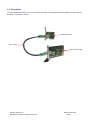
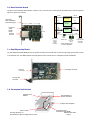
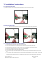
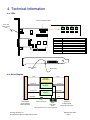
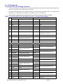
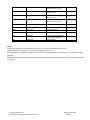
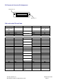
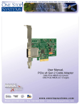
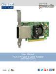
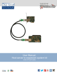
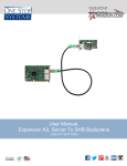
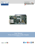
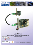
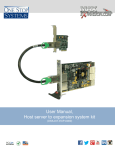
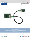
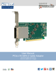
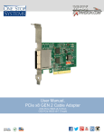
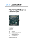
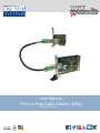
User Manual, PCIe x4 Host Cable Adapter (HIB2) OSS-KIT-EXP-4500 Table of Contents 1. Description 1.a. Description ..................................................................................................................................... 3 1.b. Host interface board ....................................................................................................................... 4 1.c. Host expansion board ..................................................................................................................... 4 1.d. Conceptual architecture.................................................................................................................. 4 2. Specifications 2.a. Host interface board ....................................................................................................................... 5 2.b. Host expansion board..................................................................................................................... 5 3. Installation Instructions 3.a. Connecting PCIe cable.................................................................................................................... 6 3.b. Removing PCIe cable...................................................................................................................... 6 3.c. Installation instructions for a 2-slot backplane ................................................................................. 6 4. Technical Information 4.a. LEDs .................................................................................................................................................. 7 4.b. Block Diagram ................................................................................................................................... 7 4.c. Pin assignments ................................................................................................................................. 8 4.d. Signal Descriptions ............................................................................................................................ 12 5. Ordering Information One Stop Systems, Inc. Specifications subject to change without notice OSS-KIT-EXP-4500 Page 2 1.a. Description The Host Interface Board (HIB2) sits in the host machine and cables to the Host Expansion Board (HEB2). The Host Expansion Board site in a CPCI/CPCE Chassis. Host interface board PCIe x4 cable Host expansion board One Stop Systems, Inc. Specifications subject to change without notice OSS-KIT-EXP-4500 Page 3 1.b. Host interface board The PCIe x4 host Interface board installs in a PCIe x4, x8, or x16 PCIe slot of a host system and cables down to a PCIe expansion system or other PCIe x4 device. Clock* Clock* LVPECL Clock Buffer Slot Cover (Also available in low profile height) 3.35” Power on / Cable Ready LEDs PCIe x4 Connect or 2.713” X4 PCIe Tx PCIe Signal Redriver X4 PCIe Rx PCIe Signal Redriver CPRS NT# Downstream X4 PCI Express Cable Connector X4 PCIe X4 PCIe Rx +3.3v LEDs Cable Present/ Pwr LEDs PCIe lane status *Clock direction shown in Host configuration Upstream X4 PCI Express Card Edge Connector 1.c. Host Expansion Board The Host Expansion Board (HEB2) fits into the system slot of the CPCI chassis and connects through a high-speed PCIe x4 cable to an upstream host. The HEB2 expands the PCI Express bus from a PCIe slot to a CompactPCI system at 20Gb/sec. PCIe x4 connector Card edge connector Locking card connector 1.d. Conceptual architecture Upstream host adapter PCIe backplane in the host enclosure Compact PCI backplane PCIe x4 cable One Stop Systems, Inc. Specifications subject to change without notice Downstream host expansion board (HEB2) OSS-KIT-EXP-4500 Page 4 2 Specifications 2.a. Host interface board specifications Electrical/Mechanical Specifications Form Factor: ExpressCard/34 Dimensions (H x L): 1.34 x 5.01 inches (34 x 127.3mm) External Connectors: One PCIe x4 cable connector Board Indicators: Power On / Cable Present LEDs Power Consumption (designed to meet the following conditions 3W typical, 3.3V@1A Operating Environment (designed to meet the following conditions) Temperature Range: 0° to 55°C (32° to 131°F) Relative Humidity: 10 to 90% non-condensing Shock: 30g acceleration peak (11ms pulse) no cable connected Vibration: 5-17 Hz 0.5” double amplitude displacement; 7-2000Hz, 1.5g acceleration. Redriver Pericom PIEQX4401 Agency Compliance Designed to meet, but not tested UL60950, FCC Class B, CE safety and emissions 2.b. Host expansion board specifications CPCI Interface Cable Interface Electrical/Mechanical Operating Environment Agency Compliance: 32 or 64 bit at 66 or 33MHz 3.3V I/O only Internal arbiter supports up to 4 external masters Seven CPCI slots (up to 7 PCI clock/bus requests) Enhanced Intel SpeedStep Technology Single port x4 link width 100MHz reference clock 256 byte maximum payload size Automatic link training (auto-negotiate to largest common width) Advance flow control, CRC and error reporting Molex 75586-0010 connector 3U or 6U CPCI system master or peripheral slot 3U [H x L x W] dimensions of 3.937 x 6.299 x 0.6” (100 x 160 x 1.6mm) Tundra Tsi384 32/64-Bit/33/66MHz CPCI bus on connectors J1 & J2 Four green front panel indicators Automatic downstream select cable dip switches Temperature range 0 to 50C (32 to 122F) Relative Humidity 5 to 90% non-condensing Shock: 5-17 Hz 0.5” double amplitude displacement; 7-2000Hz, 1.5g acceleration +Designed to meet UL 60950, FCC Class B, CE safety and emissions One Stop Systems, Inc. Specifications subject to change without notice OSS-KIT-EXP-4500 Page 5 3. Installation Instructions 3.a. Connecting PCIe cable 1) To install the PCIe cable, Insert into the expansion link board firmly or until you feel it lock into place. 3.b. Removing PCIe cable: 1) To remove PCIe cable pull back on green thumb tab to release metal pins and gently separate. 3.c. Installation instructions for a 2-slot backplane 1) Insert the HIB2 x4 in host mode in a PCIe slot in the host computer 2) Connect the 2-slot backplane to an ATX power supply separate from the host system power supply. 3) Insert the HIB2 x4 in target mode in the PCIe connector on the test backplane, next to the ATX connector. 4) Insert the PCIe endpoint board in the other PCIe slot on the test backplane. 5) Connect the PCIe cable to both the host and target HIB2 x4. 6) Turn on the power supply for the test backplane. NOTE: The power supply and test backplane will not power up at this time. 7) Turn on the host system. Signals across the PCIe cable will cause the test backplane to power up as well. The power and cable LEDS on both HIB2 x4s should be on, indicating that the host system is communicating with the endpoint board. One Stop Systems, Inc. Specifications subject to change without notice OSS-KIT-EXP-4500 Page 6 4. Technical Information 4.a. LEDs PCIe Lane Status LEDs Power and Cable present LEDs CR2 CR4 CR6 CR8 CR3 CR5 CR7 CR9 LED # CR2 CR3 CR4 CR5 CR6 CR7 CR8 CR9 Cable present LED Function Tx pair, Lane 0 (from card edge) Rx pair, Lane 0 (from cable) Tx pair, Lane 1 (from card edge) Rx pair, Lane 1 (from cable) Tx pair, Lane 2 (from card edge) Rx pair, Lane 3 (from cable) Tx pair, Lane 3 (from card edge) Rx pair, Lane 2 (from cable) Power LED 4.b. Block Diagram Clock* Clock* LVPECL Clock Buffer x4 PCIe Tx PCIe Signal Redriver x4 PCIe Rx PCIe Signal Redriver x4 PCIe Tx x4 PCIe Rx +3.3v CPRSNT# Downstream x4 PCI Express Cable Connector LEDs Cable Present/ Pwr LEDs PCIe lane status Upstream x4 PCI Express Card Edge Connector *Clock direction shown in Host configuration One Stop Systems, Inc. Specifications subject to change without notice OSS-KIT-EXP-4500 Page 7 4.c. Pin Assignments Connectors PCIe x4 Card Edge Connector The pins are numbered as shown with side A on the top of the centerline on the solder side of the board and side B on the bottom of the centerline on the component side of the board. The PCIe interface pins PETpx, PETnx, PERpx, and PERnx are named with the following convention: “PE” stands for PCIe high speed, “T” for Transmitter, “R” for Receiver, “p” for positive (+), and “n” for negative (-). Note that adjacent differential pairs are separated by two ground pins to manage the connector crosstalk. Table 1: Pin-out for the PCIe x4 Card Edge Connector on the Host Cable Adapter Pin # Side B Side A Name Description Name Description 1 N/C N/C PRSNT1# Hot-Plug presence detect 2 N/C N/C N/C N/C 3 N/C N/C N/C N/C 4 GND Ground GND Ground 5 NC N/C N/C Not connected 6 N/C N/C JTAG3 Host Mode:TDI (Test Data Input) Target Mode: Test Clock+ 7 GND Ground JTAG4 Host Mode: TDO (Test Data Output) Target Mode: Test Clock- 8 +3.3V 3.3 V power N/C Not connected 9 N/C Host Mode: Not connected Target Mode: Test Power On N/C Not connected 10 3.3Vaux 3.3 V auxiliary power +3.3V 3.3 V power 11 N/C N/C PERST# Fundamental reset Mechanical key 12 RSVD Reserved GND 13 GND Ground REFCLK+ 14 PETp0 15 PETn0 Transmitter differential pair, Lane 0 16 GND Ground PERp0 17 PRSNT2# Hot-Plug presence detect PERn0 18 GND Ground GND Ground 19 PETp1 Reserved PETn1 Transmitter differential pair, Lane 1 RSVD 20 GND Ground 21 GND Ground PERp1 22 GND Ground PERn1 23 PETp2 24 PETn2 Transmitter differential pair, Lane 2 25 GND Ground PERp2 26 GND Ground PERn2 27 PETp3 28 PETn3 Transmitter differential pair, Lane 3 29 GND Ground PERp3 30 RSVD Reserved PERn3 31 PRSNT2# Hot-Plug presence detect GND Ground 32 GND Ground RSVD Reserved One Stop Systems, Inc. Specifications subject to change without notice REFCLK GND Ground Reference clock (differential pair) Ground Receiver differential pair, Lane 0 Receiver differential pair, Lane 1 GND Ground GND Ground Receiver differential pair, Lane 2 GND Ground GND Ground Receiver differential pair, Lane 3 OSS-KIT-EXP-4500 Page 8 PCI Table 2: Pin-out for the External PCIe Cable Connector PIN # Signal Description A1 GND A2 PETp0 A3 PETn0 A4 GND A5 PETp1 A6 PETn1 A7 GND A8 PETp2 A9 PETn2 A10 GND A11 PETp3 A12 PETn3 A13 GND A14 CREFCLK+ A15 CREFCLK A16 GND A17 SB_RTN A18 CPRSNT# Ground reference for PCI Express transmitter Lanes Differential PCI Express transmitter Lane 0 5 Differential PCI Express transmitter Lane 0 5 GND Ground reference for PCI Express transmitter Lanes Differential PCI Express transmitter Lane 1 5 Differential PCI Express transmitter Lane 1 Ground reference for PCI Express transmitter Lanes Differential PCI Express transmitter Lane 2 Differential PCI Express transmitter Lane 2 Ground reference for PCI Express transmitter Lanes Differential PCI Express transmitter Lane 3 Differential PCI Express transmitter Lane 3 Ground reference for PCI Express transmitter Lanes Differential 100MHz cable reference clock Differential 100MHz cable reference clock GND Ground reference for cable reference clock Signal return for single ended sideband signals Used for detection of whether a cable is installed and the downstream subsystem is powered A19 CPWRON B1 GND B2 PERp0 B3 PERn0 B4 GND B5 PERp1 B6 PERn1 B7 GND B8 PERp2 B9 PERn2 One Stop Systems, Inc. Specifications subject to change without notice Notes 5 5 5 5 5 5 5 5 Turns power on / off to slavetype downstream subsystems Ground reference for PCI Express receiver Lanes Differential PCI Express receiver Lane 0 Differential PCI Express receiver Lane 0 Ground reference for PCI Express receiver Lanes 5 Differential PCI Express receiver Lane 1 Differential PCI Express receiver Lane 1 Ground reference for PCI Express receiver Lanes 5 Differential PCI Express receiver Lane 2 Differential PCI Express receiver Lane 2 5 5 5 5 OSS-KIT-EXP-4500 Page 9 B10 GND Ground reference for PCI Express receiver Lanes B11 PERp3 Differential PCI Express receiver Lane 3 5 B12 PERn3 Differential PCI Express receiver Lane 3 5 B13 GND Ground reference for PCI Express receiver Lanes B14 PWR +3.3VCable power B15 PWR +3.3VCable Power B16 PWR RTN Cable power return B17 PWR RTN Cable power return B18 CWAKE# Power management signal for wakeup events (optional) B19 CPERST# Cable PERST# 1, 3 Notes: 1 Optional signals that are not implemented are to be left as no connects on the board side connector. 2 Reserved signals must be left as no connects on the board side connector. 3 Although support of CWAKE# is optional from the board side connector perspective, an allocated wire is mandated for the cable assembly. 4 Board side pin-out on both sides of the Link is identical. The cable assembly incorporates a null modem for the PCIe transmit and receive pairs. One Stop Systems, Inc. Specifications subject to change without notice OSS-KIT-EXP-4500 Page 10 PCI Express x4 Connector Pin Assignment Row B, Pin 19 Row A, Pin 1 PIN- out for the PCIe x4 Cable Pin # A1 A4 A7 A10 A13 A16 B1 B4 B7 B10 B13 A2 A3 A5 A6 Cable Side 1 GND Pin # A8 A9 A11 A12 A14 A15 A17 A18 A19 B2 B3 B5 B6 B8 B9 B11 B12 B14 B15 B16 B17 B18 B19 Cable Side 1 PETp2 PETn2 PETp3 PETn3 CREFCLK+ CREFCLK SB_RTN CPRSNT# CPWRON PERp0 PERn0 PERp1 PERn1 PERp2 PERn2 PERp3 PERn3 PWR PWR PWR_RTN PWR_RTN CWAKE# CPERST# Backshell Chassis Ground PETp0 PETn0 PETp1 PETn1 Drain Wires Differential Pair Differential Pair Differential Pair Differential Pair Differential Pair Hook-up Wire Hook-up Wire Hook-up Wire Differential Pair Differential Pair Differential Pair Differential Pair NC NC NC NC Hook-up Wire Hook-up Wire Overall Cable Braid One Stop Systems, Inc. Specifications subject to change without notice Cable Side 2 GND PERp0 PERn0 PERp1 PERn1 Pin # A1 A4 A7 A10 A13 A16 B1 B4 B7 B10 B13 B2 B3 B5 B6 Cable Side 2 PERp2 PERn2 PERp3 PERn3 CREFCLK+ CREFCLKSB_RTN CPRSNT# CPWRON PETp0 PETn0 PETp1 PETn1 PETp2 PETn2 PETp3 PETn3 PWR PWR PWR_RTN PWR_RTN CWAKE# CPERST# Pin # B8 B9 B11 B12 A14 A15 A17 A18 A19 A2 A3 A5 A6 A8 A9 A11 A12 B14 B15 B16 B17 B18 B19 Chassis Ground Back shell OSS-KIT-EXP-4500 Page 11 4.d. Signal Descriptions PETp(x) PCI Express Transmit Positive signal of (x) pair. PETn(x) PCI Express Transmit Negative signal of (x) pair. PERp(x) PCI Express Receive Positive signal of (x) pair. PERn(x) PCI Express Receive Negative signal of (x) pair. Cable REFerence CLocK: Provides a reference clock from the host system to the remote system. Side Band ReTurN: return path for single ended signals from remote systems. CREFCLK+/SB_RTN CPRSNT# PWR_RTN Cable PReSeNT: Indicates the presence of a device beyond the cable. PoWeR: Provides local power for in-cable redriver circuits. Only needed on long cables. Power does not go across the cable.) PoWeR ReTurN: Provides local power return path for PWR pins. CWAKE# Cable WAKE CPERST# Cable PCI Express Reset PWR One Stop Systems, Inc. Specifications subject to change without notice OSS-KIT-EXP-4500 Page 12 5. Ordering Information OSS-KIT-EXP-4500 One Stop Systems, Inc. Rev. A OSS-KIT-EXP-4500 Page 13