1
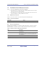
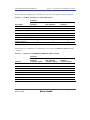
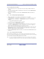
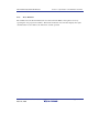
User’s Manual
H8S, H8SX Family E10A-USB Emulator
Additional Document for User’s Manual
Supplementary Information on Using the H8S/2113 Group
H8S Family / H8S/2100 Series
E10A-USB for H8S/2113
HS2113KCU01HE
All information contained in these materials, including products and product specifications,
represents information on the product at the time of publication and is subject to change by
Renesas Electronics Corporation without notice. Please review the latest information published
by Renesas Electronics Corporation through various means, including the Renesas Electronics
Corporation website (http://www.renesas.com).
www.renesas.com
Rev.1.00 Mar. 2013
Notice
1.
Descriptions of circuits, software and other related information in this document are provided only to illustrate the operation of
semiconductor products and application examples. You are fully responsible for the incorporation of these circuits, software,
and information in the design of your equipment. Renesas Electronics assumes no responsibility for any losses incurred by you
or third parties arising from the use of these circuits, software, or information.
2.
Renesas Electronics has used reasonable care in preparing the information included in this document, but Renesas Electronics
does not warrant that such information is error free. Renesas Electronics assumes no liability whatsoever for any damages
incurred by you resulting from errors in or omissions from the information included herein.
3.
Renesas Electronics does not assume any liability for infringement of patents, copyrights, or other intellectual property rights of
third parties by or arising from the use of Renesas Electronics products or technical information described in this document. No
license, express, implied or otherwise, is granted hereby under any patents, copyrights or other intellectual property rights of
Renesas Electronics or others.
4.
You should not alter, modify, copy, or otherwise misappropriate any Renesas Electronics product, whether in whole or in part.
Renesas Electronics assumes no responsibility for any losses incurred by you or third parties arising from such alteration,
modification, copy or otherwise misappropriation of Renesas Electronics product.
5.
Renesas Electronics products are classified according to the following two quality grades: “Standard” and “High Quality”. The
recommended applications for each Renesas Electronics product depends on the product’s quality grade, as indicated below.
“Standard”:
Computers; office equipment; communications equipment; test and measurement equipment; audio and visual
equipment; home electronic appliances; machine tools; personal electronic equipment; and industrial robots etc.
“High Quality”: Transportation equipment (automobiles, trains, ships, etc.); traffic control systems; anti-disaster systems; anticrime systems; and safety equipment etc.
Renesas Electronics products are neither intended nor authorized for use in products or systems that may pose a direct threat to
human life or bodily injury (artificial life support devices or systems, surgical implantations etc.), or may cause serious property
damages (nuclear reactor control systems, military equipment etc.). You must check the quality grade of each Renesas
Electronics product before using it in a particular application. You may not use any Renesas Electronics product for any
application for which it is not intended. Renesas Electronics shall not be in any way liable for any damages or losses incurred
by you or third parties arising from the use of any Renesas Electronics product for which the product is not intended by Renesas
Electronics.
6.
You should use the Renesas Electronics products described in this document within the range specified by Renesas Electronics,
especially with respect to the maximum rating, operating supply voltage range, movement power voltage range, heat radiation
characteristics, installation and other product characteristics. Renesas Electronics shall have no liability for malfunctions or
damages arising out of the use of Renesas Electronics products beyond such specified ranges.
7.
Although Renesas Electronics endeavors to improve the quality and reliability of its products, semiconductor products have
specific characteristics such as the occurrence of failure at a certain rate and malfunctions under certain use conditions. Further,
Renesas Electronics products are not subject to radiation resistance design. Please be sure to implement safety measures to
guard them against the possibility of physical injury, and injury or damage caused by fire in the event of the failure of a Renesas
Electronics product, such as safety design for hardware and software including but not limited to redundancy, fire control and
malfunction prevention, appropriate treatment for aging degradation or any other appropriate measures. Because the evaluation
of microcomputer software alone is very difficult, please evaluate the safety of the final products or systems manufactured by
you.
8.
Please contact a Renesas Electronics sales office for details as to environmental matters such as the environmental compatibility
of each Renesas Electronics product. Please use Renesas Electronics products in compliance with all applicable laws and
regulations that regulate the inclusion or use of controlled substances, including without limitation, the EU RoHS Directive.
Renesas Electronics assumes no liability for damages or losses occurring as a result of your noncompliance with applicable laws
and regulations.
9.
Renesas Electronics products and technology may not be used for or incorporated into any products or systems whose
manufacture, use, or sale is prohibited under any applicable domestic or foreign laws or regulations. You should not use
Renesas Electronics products or technology described in this document for any purpose relating to military applications or use
by the military, including but not limited to the development of weapons of mass destruction. When exporting the Renesas
Electronics products or technology described in this document, you should comply with the applicable export control laws and
regulations and follow the procedures required by such laws and regulations.
10. It is the responsibility of the buyer or distributor of Renesas Electronics products, who distributes, disposes of, or otherwise
places the product with a third party, to notify such third party in advance of the contents and conditions set forth in this
document, Renesas Electronics assumes no responsibility for any losses incurred by you or third parties as a result of
unauthorized use of Renesas Electronics products.
11. This document may not be reproduced or duplicated in any form, in whole or in part, without prior written consent of Renesas
Electronics.
12. Please contact a Renesas Electronics sales office if you have any questions regarding the information contained in this document
or Renesas Electronics products, or if you have any other inquiries.
(Note 1) “Renesas Electronics” as used in this document means Renesas Electronics Corporation and also includes its majorityowned subsidiaries.
(Note 2) “Renesas Electronics product(s)” means any product developed or manufactured by or for Renesas Electronics.
(2012.4)
Regulatory Compliance Notices
European Union regulatory notices
This product complies with the following EU Directives. (These directives are only valid in the European Union.)
CE Certifications:
• Electromagnetic Compatibility (EMC) Directive 2004/108/EC
EN 55022 Class A
WARNING: This is a Class A product. In a domestic environment this product may
cause radio interference in which case the user may be required to take adequate
measures.
EN 55024
• Information for traceability
• Authorised representative
Name:
Renesas Electronics Corporation
Address:
1753, Shimonumabe, Nakahara-ku, Kawasaki, Kanagawa, 211-8668, Japan
• Manufacturer
Name:
Renesas Solutions Corp.
Address:
Nippon Bldg., 2-6-2, Ote-machi, Chiyoda-ku, Tokyo 100-0004, Japan
• Person responsible for placing on the market
Name:
Renesas Electronics Europe Limited
Address:
Dukes Meadow, Millboard Road, Bourne End, Buckinghamshire, SL8 5FH, U.K.
Environmental Compliance and Certifications:
• Waste Electrical and Electronic Equipment (WEEE) Directive 2002/96/EC
WEEE Marking Notice (European Union Only)
Renesas development tools and products are directly covered by the European Union's Waste
Electrical and Electronic Equipment, (WEEE), Directive 2002/96/EC. As a result, this equipment,
including all accessories, must not be disposed of as household waste but through your locally
recognized recycling or disposal schemes. As part of our commitment to environmental
responsibility Renesas also offers to take back the equipment and has implemented a Tools Product
Recycling Program for customers in Europe. This allows you to return equipment to Renesas for
disposal through our approved Producer Compliance Scheme. To register for the program, click
here “http://www.renesas.com/weee".
United States Regulatory notices on Electromagnetic compatibility
FCC Certifications (United States Only):
This equipment has been tested and found to comply with the limits for a Class A digital device, pursuant to Part
15 of the FCC Rules. These limits are designed to provide reasonable protection against harmful interference
when the equipment is operated in a commercial environment. This equipment generates, uses, and can radiate
radio frequency energy and, if not installed and used in accordance with the instruction manual, may cause
harmful interference to radio communications. Operation of this equipment in a residential area is likely to cause
harmful interference in which case the user will be required to correct the interference at his own expense.
CAUTION:
Changes or modifications not expressly approved by the party responsible for
compliance could void the user's authority to operate the equipment.
Table of Contents
Section 1
1.1
1.2
1.3
1.4
Section 2
2.1
2.2
Connecting the Emulator with the User System ............................................................... 1
Components of the E10A-USB Emulator ................................................................................................................. 1
Connecting the E10A-USB Emulator with the User System .................................................................................... 2
Pin Assignments of the E10A-USB Connector......................................................................................................... 3
Example of Emulator Connection............................................................................................................................. 4
Specifications of the Emulator’s Software ....................................................................... 7
Differences between the H8S/2113 and the Emulator .............................................................................................. 7
The H8S/2113 E10A-USB Emulator Functions ..................................................................................................... 10
2.2.1
Emulator Driver Selection............................................................................................................................ 10
2.2.2
Hardware Break Functions ........................................................................................................................... 10
2.2.3
Notes on Setting the [Breakpoint] Dialog Box............................................................................................. 12
2.2.4
Note on Using the JTAG Clock (TCK) ........................................................................................................ 12
2.2.5
Trace Function.............................................................................................................................................. 13
H8S, H8SX Family E10A-USB Emulator
Section 1 Connecting the Emulator with the User System
Section 1 Connecting the Emulator with the User System
1.1
Components of the E10A-USB Emulator
The H8S/2113 E10A-USB emulator supports the H8S/2113 (hereafter referred to as the MCU
unless the description is specific to any of them). Table 1.1 lists the components of the emulator.
Table 1.1 Components of the Emulator
Classification Component
Hardware
Appearance
Emulator box
Quantity
1
Remarks
HS0005KCU01H:
Depth: 65.0 mm, Width: 97.0 mm,
Height: 20.0 mm, Mass: 72.9 g
or
HS0005KCU02H:
Depth: 65.0 mm, Width: 97.0 mm,
Height: 20.0 mm, Mass: 73.7 g
Software
User system interface
cable
1
14-pin type:
Length: 20 cm, Mass: 33.1 g
USB cable
1
Length: 150 cm, Mass: 50.6 g
H8S/2113 E10A-USB
emulator setup
program,
1
HS0005KCU01SR,
H8S, H8SX Family
E10A-USB Emulator
User’s Manual,
HS0005KCU01HJ-H8S,
HS0005KCU01HE-H8S,
Supplementary
Information on Using
the H8S/2113*, and
HS2113KCU01HJ,
HS2113KCU01HE,
Test program manual
for HS0005KCU01H
and HS0005KCU02H
HS0005TM01HJ, and
HS0005TM01HE
(provided on a CD-R)
Note: Additional document for the MPUs supported by the emulator is included. Check the target
MPU and refer to its additional document.
R20UT2527EJ0100 Rev. 1.00
Mar 19, 2013
Page 1 of 14
H8S, H8SX Family E10A-USB Emulator
1.2
Section 1 Connecting the Emulator with the User System
Connecting the E10A-USB Emulator with the User System
Before connecting an E10A-USB emulator (hereafter referred to as emulator) with the user
system, a connector must be installed in the user system so that an user system interface cable can
be connected. When designing the user system, refer to an example of recommended connection
between the connector and the MCU shown in this manual.
Before designing the user system, be sure to read the E10A-USB emulator user’s manual and the
hardware manual for related MCUs.
Connect pins 8, 9, 10, 12, 13, and 14 of the user system connector to GND firmly on the PCB.
These pins are used as electrical GND and to monitor the connection of the user system connector.
Note the pin assignments of the user system connector.
User system interface cable
Tab
GND line
User system connector
Pin 8
User system GND
connection
Pin 1
User system
Figure 1.1 Connecting the User System Interface Cable to the User System
Notes: 1. The pin number assignments of the 14-pin connector differ from those of the E8a
emulator; however, the physical location is the same.
2. When designing the connector layout on the user board, do not place any components
within 3 mm of the connector.
R20UT2527EJ0100 Rev. 1.00
Mar 19, 2013
Page 2 of 14
H8S, H8SX Family E10A-USB Emulator
Section 1 Connecting the Emulator with the User System
WARNING
Be sure to place the GND line of the user system interface
cable on the GND of the user system with a screw, etc. Failure
to do so will result in a FIRE HAZARD due to an overcurrent
and will damage the user system, the emulator product, and
the host computer.
1.3
Pin Assignments of the E10A-USB Connector
Figure 1.2 shows the pin assignments of the user system connector.
Pin No.
Pin 1 mark
User system connector
User system connector
(top view)
Pin 14
Pin 7
Pin 8
Pin 1
Pin 1 mark
Input/Output *1
1
PE1/ETCK
Input
2
PE5/ETRST#
Input
3
PE3/ETDO
Output
4
RES(in)# *2 *6
Input
5
PE4/ETMS
Input
6
PE2/ETDI
Input
7
RES(out)# *2
Output
8 to 10
GND *3
12 to 14
11
Top view
MCU Pin Name
H8S/2113 *5
Vcc *4
Notes: 1. Input to or output of the user system connector on the user system.
2. The symbol (#) means that the signal is active-low.
3. By detecting GND on the user system side, the emulator
decides whether the user system is connected or not.
4. Connect Vcc with the Vcc of the MCU.
5. When using E10A-USB, these pins are used only for E10A-USB
connector pins, therefore PE1 to PE5 pin functions are not available.
6. RES(in) is not the pin name of the MCU. It cannot be directly
connected to the MCU pins.
Figure 1.2 Pin Assignments of the User System Connector
R20UT2527EJ0100 Rev. 1.00
Mar 19, 2013
Page 3 of 14
H8S, H8SX Family E10A-USB Emulator
1.4
Section 1 Connecting the Emulator with the User System
Example of Emulator Connection
The figure shown below is an example of connecting the user system to the emulator.
14-pin connector with
a 2.54-mm pitch
(3M Limited: 7614-6002)
Pulled-up at 4.7 kΩ
Vcc
MCU
11
MD2
1
PE1/ETCK
2
PE5/ETRST#
3
PE3/ETDO
5
PE4/ETMS
6
PE2/ETDI
4
User logic
7
RES#
8 to 10
12 to 14
E10A-USB pin No.
User system
· RES(in)# of pin 4 of the user system connector is a signal line in which the emulator outputs signals to the MCU.
Connect RES(in)# of pin 4 and the user system reset circuit to the MCU, as shown above.
· RES(out)# of pin 7 of the user system connector is a signal line in which the emulator monitors the RES# signal of
the MCU. The RES(out)# must be pulled up before it is connected to pin 7 of the user system connector.
Figure 1.3 Example of Emulator Connection
R20UT2527EJ0100 Rev. 1.00
Mar 19, 2013
Page 4 of 14
H8S, H8SX Family E10A-USB Emulator
Section 1 Connecting the Emulator with the User System
Notes: 1. The emulator uses PE1 to PE5 pins. Pull up the emulator and MCU pins and connect
them to the user system connector.
MCU
User system
connector
Vcc
4.7 k
Pins 1, 2, 3, 5, and 6
Figure 1.4 Connection of Emulator and the MCU
2.
RES(in)# of pin 4 of the user system connector is a signal line in which the
emulator outputs signals to the MCU. RES(in)# of pin 4 and the user system reset
circuit must be connected to the MCU, as shown in figure 1.5. RES(out)# of pin 7
of the user system connector is a signal line in which the emulator monitors the
RES# signal of the MCU. The RES# must be pulled up before it is connected to pin
7 of the user system connector.
Vcc
4.7 kΩ
User system
connector
User
logic
MCU
Vcc
RES(in)# (pin 4)
4.7 kΩ
RES#
RES(out)# (pin 7)
Figure 1.5 Example of Reset Circuits
3.
Connect GND of pins 8 to 10, 12 to 14 of the user system connector to ground in the
user system.
4.
Connect Vcc, pin 11 of the user system connector, to the power supply (Vcc) in the
user system. The input voltage, Vcc, is within the range of guaranteed operation of
the microcomputer.
5.
When the emulator is used, the pin functions listed below are not available.
R20UT2527EJ0100 Rev. 1.00
Mar 19, 2013
Page 5 of 14
H8S, H8SX Family E10A-USB Emulator
Section 1 Connecting the Emulator with the User System
Table 1.2 Pin Functions Not Available
H8S/2113
PE1 to PE5
The symbol ‘#’ means that the signal is active-low.
R20UT2527EJ0100 Rev. 1.00
Mar 19, 2013
Page 6 of 14
H8S, H8SX Family E10A-USB Emulator
Section 2 Specification of the Emulator’s Software
Section 2 Specifications of the Emulator’s Software
2.1
Differences between the H8S/2113 and the Emulator
1. When the emulator system is initiated, it initializes the general registers and part of the control
registers as shown in table 2.1. The initial value of the MCU is undefined. When the emulator
is initiated from the workspace, a value to be entered is saved in a session.
For the registers shown in table 2.1, values other than PC or CCR are not changed even if the
CPU reset command is issued. If ER7 (SP) is changed as an odd value, it must be modified in
the [Register] window.
Table 2.1 Register Initial Values at Emulator Power-On
Register
Initial Value
PC
Reset vector value in the vector address table
ER0 to ER6
H’0
ER7 (SP)
H'10
CCR
1 for I mask, and others undefined
EXR
H’7F
MACH
H’0
MACL
H’0
2. System Control Register
In the emulator, the internal I/O registers can be accessed from the [IO] window. However, be
careful when accessing the system control register. The emulator saves the register value of the
system control register at a break and returns the value when the user program is executed.
Since this is done during a break, do not rewrite the system control register in the [IO]
window.
3. Memory Access during Emulation
If the memory contents are referenced or modified during emulation, realtime emulation
cannot be performed because the user program is temporarily halted.
4. The emulator communicates with the MCU by using the PE1 to PE5 pins. These pins cannot
be used.
R20UT2527EJ0100 Rev. 1.00
Mar 19, 2013
Page 7 of 14
H8S, H8SX Family E10A-USB Emulator
Section 2 Specification of the Emulator’s Software
5. When the emulator is used, the power consumed by the MCU can reach several mA. This is
because the user power supply drives ICs to make the communication signal level match the
user-system power-supply voltage.
6. Do not use an MCU that has been used for debugging.
If the flash memory is rewritten many times, and the MCU is left for a few days, data may be
lost due to retention problems.
If the flash memory is rewritten many times, the data will not be erased. If an error message is
displayed, exchange the MCU for a new one.
7. MCU Operating Mode
The emulator supports mode 6 (on-chip emulation mode). Use mode 6 for emulation in mode
2.
8. Programming Flash Memory during Debugging
The flash memory is programmed in the following functions because they use breakpoints:
• When executing [Go to cursor]
• When stepping over the subroutine
• When executing the subroutine at step-out operation
9. Sum Data Displayed in the Program Flash Mode
Sum data, which is displayed in the ‘Program Flash’ mode, is a value that data in the whole
ROM areas has been added by bytes.
10. Note on Executing the User Program
The set value is rewritten since the emulator uses flash memory and watchdog timer registers
during programming (Go, Step In, Step Out, or Step Over) of the flash memory.
11. Loading Sessions
⎯ Information in [JTAG clock] of the [Configuration] dialog box cannot be recovered by
loading sessions. Thus the value of the JTAG clock (TCK) becomes the initial value at
execution of start-up.
R20UT2527EJ0100 Rev. 1.00
Mar 19, 2013
Page 8 of 14
H8S, H8SX Family E10A-USB Emulator
Section 2 Specification of the Emulator’s Software
12. Value Set in the [System Clock] Dialog Box when Connecting the Emulator
Input the frequency of the oscillator in use in the [System Clock] dialog box (this also applies
when the MCU is multiplied by the PLL circuit).
Figure 2.1 [System Clock] Dialog Box
13. Emulation on Programming or Erasing the Internal Flash Memory
A break cannot be generated while the program for programming or erasing the internal flash
memory is being called. Note that the following processing also cannot be performed:
• Execution of the [STOP] button
• Auto-update of the watch function and use of the tool-chip watch function
• Memory operation during executing emulation
14. Table 2.2 shows a list of device supported by the H8S/2113 emulator.
Table 2.2 A List of Device Supported by the Emulator
Project Target
Device
H8S/2113 E10A-USB SYSTEM (CPU2100)
H8S/2113
R20UT2527EJ0100 Rev. 1.00
Mar 19, 2013
Page 9 of 14
H8S, H8SX Family E10A-USB Emulator
2.2
Section 2 Specification of the Emulator’s Software
The H8S/2113 E10A-USB Emulator Functions
Notes: 1. Do not use an MCU that has been used for debugging.
2. If the flash memory is rewritten many times, and the emulator is left for a few days,
data may be lost due to retention problems.
3. If the flash memory is rewritten many times, the data will not be erased. If an error
message is displayed, exchange the MCU for a new one.
2.2.1
Emulator Driver Selection
Table 2.3 shows drivers which can be selected in the [Driver Details] dialog box.
Table 2.3 Type Name and Driver
Type Name
Driver
HS0005KCU01H, HS0005KCU02H
Renesas E-Series USB Driver
2.2.2
Hardware Break Functions
Hardware Break Conditions: In the H8S/2113 E10A-USB emulator, eight break conditions
(Break Condition 1,2,3,4,5,6,7,8) can be set. Table 2.4 lists the items that can be specified.
Table 2.4 Hardware Break Condition Specification Items
Items
Description
Address bus condition
Breaks when the MCU address bus value matches the
specified value.
Data bus condition
Breaks when the MCU data bus value matches the specified
value. High or low byte or word can be specified as the
access data size.
Read or write condition
Breaks in the read or write cycle.
Trace acquisition condition
Acquires trace information based on Break Condition 1.
R20UT2527EJ0100 Rev. 1.00
Mar 19, 2013
Page 10 of 14
H8S, H8SX Family E10A-USB Emulator
Section 2 Specification of the Emulator’s Software
Table 2.5 lists the combinations of conditions that can be set in the [Break condition] dialog box.
Table 2.5 Conditions Set in [Break condition] Dialog Box
Condition
Dialog Box
Address Bus
Condition
Data Condition
Read or Write
Condition
[Break condition 1]
O
O
O
[Break condition 2]
O
O
O
[Break condition 3]
O
X
O
[Break condition 4]
O
X
O
[Break condition 5]
O
X
O
[Break condition 6]
O
X
O
[Break condition 7]
O
X
O
[Break condition 8]
O
X
O
Note: O: Can be set by checking the radio button in the dialog box.
Table 2.6 lists the combinations of conditions that can be set by the BREAKCONDITION_SET
command.
Table 2.6 Conditions Set by BREAKCONDITION_SET Command
Condition
Channel
Address Bus
Condition
(<addropt> option)
Data Condition
(<dataopt> option)
Read or Write
Condition
(<r/wopt> option)
Break condition 1
O
O
O
Break condition 2
O
O
O
Break condition 3
O
X
O
Break condition 4
O
X
O
Break condition 5
O
X
O
Break condition 6
O
X
O
Break condition 7
O
X
O
Break condition 8
O
X
O
Note: O: Can be set by the BREAKCONDITION_SET command.
R20UT2527EJ0100 Rev. 1.00
Mar 19, 2013
Page 11 of 14
H8S, H8SX Family E10A-USB Emulator
Section 2 Specification of the Emulator’s Software
Notes on Setting the Break Condition:
1. When [Step In], [Step Over], or [Step Out] is selected, the settings of Break Condition are
disabled.
2. The settings of Break Condition are disabled when an instruction to which a BREAKPOINT
has been set is executed.
3. When step over function is used, the settings of BREAKPOINT and Break Condition are
disabled.
2.2.3
Notes on Setting the [Breakpoint] Dialog Box
1. When an odd address is set, the address is rounded down to an even address.
2. A BREAKPOINT is accomplished by replacing instructions. Accordingly, it can be set only
to the flash memory or the RAM area. A BREAKPOINT cannot be set to the following
addresses:
• An area other than flash memory or RAM
• An instruction in which Break Condition is satisfied
3. During step execution, a BREAKPOINT is disabled.
4. A condition set at Break Condition is disabled immediately after starting execution when an
instruction at a BREAKPOINT is executed. A break does not occur even if a condition of
Break Condition is satisfied immediately after starting the execution.
5. When execution resumes from the breakpoint address after the program execution stops at the
BREAKPOINT, single-step execution is performed at the address before execution resumes.
Therefore, realtime operation cannot be performed.
6. Settings of BREAKPOINT and Break Condition are invalid while the STEP OVER function is
being used.
2.2.4
Note on Using the JTAG Clock (TCK)
When the JTAG clock (TCK) is used, set the frequency to lower than that of the system clock.
The value of the JTAG clock (TCK) becomes the initial TCK value that has been set at the starting
up of the emulator, after [Reset CPU] or [Reset Go] is executed*.
Note: The value of the JTAG clock (TCK) that has been set at the starting up of the emulator is
appropriately calculated on the basis of the value entered in the [System clock] dialog box.
R20UT2527EJ0100 Rev. 1.00
Mar 19, 2013
Page 12 of 14
H8S, H8SX Family E10A-USB Emulator
2.2.5
Section 2 Specification of the Emulator’s Software
Trace Function
The emulator uses the branch-instruction trace function in the MCU, and acquires a trace by
operating the user program in realtime. The branch-instruction trace function displays the eightchannel branch-source address, the mnemonic, and the operand.
R20UT2527EJ0100 Rev. 1.00
Mar 19, 2013
Page 13 of 14
H8S, H8SX Family E10A-USB Emulator
R20UT2527EJ0100 Rev. 1.00
Mar 19, 2013
Section 2 Specification of the Emulator’s Software
Page 14 of 14
H8S, H8SX Family E10A-USB Emulator
Additional Document for User’s Manual
Supplementary Information on Using the H8S/2113
Publication Date:
Rev.1.00, Mar. 19, 2013
Published by:
Renesas Electronics Corporation
http://www.renesas.com
SALES OFFICES
Refer to "http://www.renesas.com/" for the latest and detailed information.
Renesas Electronics America Inc.
2880 Scott Boulevard Santa Clara, CA 95050-2554, U.S.A.
Tel: +1-408-588-6000, Fax: +1-408-588-6130
Renesas Electronics Canada Limited
1101 Nicholson Road, Newmarket, Ontario L3Y 9C3, Canada
Tel: +1-905-898-5441, Fax: +1-905-898-3220
Renesas Electronics Europe Limited
Dukes Meadow, Millboard Road, Bourne End, Buckinghamshire, SL8 5FH, U.K
Tel: +44-1628-651-700, Fax: +44-1628-651-804
Renesas Electronics Europe GmbH
Arcadiastrasse 10, 40472 Düsseldorf, Germany
Tel: +49-211-65030, Fax: +49-211-6503-1327
Renesas Electronics (China) Co., Ltd.
7th Floor, Quantum Plaza, No.27 ZhiChunLu Haidian District, Beijing 100083, P.R.China
Tel: +86-10-8235-1155, Fax: +86-10-8235-7679
Renesas Electronics (Shanghai) Co., Ltd.
Unit 301, Tower A, Central Towers, 555 LanGao Rd., Putuo District, Shanghai, China
Tel: +86-21-2226-0888, Fax: +86-21-2226-0999
Renesas Electronics Hong Kong Limited
Unit 1601-1613, 16/F., Tower 2, Grand Century Place, 193 Prince Edward Road West, Mongkok, Kowloon, Hong Kong
Tel: +852-2886-9318, Fax: +852 2886-9022/9044
Renesas Electronics Taiwan Co., Ltd.
13F, No. 363, Fu Shing North Road, Taipei, Taiwan
Tel: +886-2-8175-9600, Fax: +886 2-8175-9670
Renesas Electronics Singapore Pte. Ltd.
80 Bendemeer Road, Unit #06-02 Hyflux Innovation Centre Singapore 339949
Tel: +65-6213-0200, Fax: +65-6213-0300
Renesas Electronics Malaysia Sdn.Bhd.
Unit 906, Block B, Menara Amcorp, Amcorp Trade Centre, No. 18, Jln Persiaran Barat, 46050 Petaling Jaya, Selangor Darul Ehsan, Malaysia
Tel: +60-3-7955-9390, Fax: +60-3-7955-9510
Renesas Electronics Korea Co., Ltd.
12F., 234 Teheran-ro, Gangnam-Gu, Seoul, 135-080, Korea
Tel: +82-2-558-3737, Fax: +82-2-558-5141
© 2013 Renesas Electronics Corporation. All rights reserved.
Colophon 2.0
H8S, H8SX Family E10A-USB Emulator
Additional Document for User’s Manual
Supplementary Information on Using the H8S/2113
R20UT2527EJ0100