1
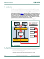
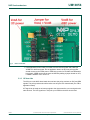
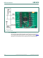
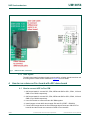
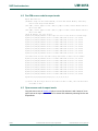
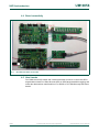
UM10856
User manual for dI2C demo board
Rev. 1 — 13 July 2015
User manual
Document information
Info
Content
Keywords
dI2C-bus, differential I2C-bus buffer, PCA9614, PCA9615, PCA9616
Abstract
User manual for the dI2C demo board OM15323. This demo board will
make it easy to test and design with PCA9614, PCA9615 and PCA9616, a
differential I2C-bus buffer.
UM10856
NXP Semiconductors
User manual for dI2C demo board
Revision history
Rev
Date
Description
1
20150713
Initial version.
Contact information
For more information, please visit: http://www.nxp.com
For sales office addresses, please send an email to: [email protected]
UM10856
User manual
All information provided in this document is subject to legal disclaimers.
Rev. 1 — 13 July 2015
© NXP Semiconductors N.V. 2015. All rights reserved.
2 of 13
UM10856
NXP Semiconductors
User manual for dI2C demo board
1. Introduction
The dI2C demo board OM13523 is for demonstration of the differential I2C-bus working
better in noise and ground offset environment than standard I2C-bus. The two dI2C demo
boards can be used to see the improvement of signal integrity in a noisy environment or a
system that has many different power sources creating different ground offset.
In the system block diagram (Figure 1), the I2C-bus between the Boot Bus Controller and
the CPU/Memory board has a lot of high speed data transmission; therefore the I2C-bus
may pick up some noise. The fan and power supply modules may have different power
sources; they may have a different ground offset level. To make a better I2C-bus system,
install dI2C devices to isolate noise and ground offset in a system.
This user manual shows how to use a dI2C demo board on an existing system.
Normal I2C-bus cable
CPU/Memory
Board
CPU/Memory
Board
Temp
sensor
Temp
sensor
Cat5, twist pair cable
Noise area
Fan
Data Switch
dI2C
dI2C
Power
Supply
dI2C
Power
Supply
dI2C
dI2C
Boot Bus
Controller
dI2C
Disk controller
Ethernet controller
USB controller
PCI slot
DVD controller
Centerplane Board
Fig 1.
Typical application
2. Key features
• A complete evaluation platform for PCA9616, (or PCA9614 and PCA9615)
• Easy to connect to an existing system
• Convenient test point for easy scope measurement and signal access
UM10856
User manual
All information provided in this document is subject to legal disclaimers.
Rev. 1 — 13 July 2015
© NXP Semiconductors N.V. 2015. All rights reserved.
3 of 13
UM10856
NXP Semiconductors
User manual for dI2C demo board
3. Getting started
3.1 Assumptions
Familiarity with the I2C-bus is recommended.
3.1.1 Static handling requirements
This device is sensitive to ElectroStatic Discharge (ESD). Therefore care should be taken
during transport and handling. You must use a ground strap or touch the PC case or other
grounded source before unpacking or handling the hardware.
3.1.2 System requirement
The OM13523 demo card can be used with Fm+ Development Board (OM13260), or
customer's application system.
3.1.3 Schematic of dI2C demo board
Fig 2.
Schematic of dI2C demo board
UM10856
User manual
All information provided in this document is subject to legal disclaimers.
Rev. 1 — 13 July 2015
© NXP Semiconductors N.V. 2015. All rights reserved.
4 of 13
UM10856
NXP Semiconductors
User manual for dI2C demo board
Fig 3.
OM13523 dI2C demo board
3.1.4 Bill of materials
Table 1.
Bill of materials
Part
Value
Package
Part #
Description
C1
100n
C0603
399-1095-1-ND
SMD capacitor
C2
22uF/16V
A/3216-18R
1276-2728-1-ND
SMD capacitor
C3
22uF/16v
A/3216-18R
1276-2728-1-ND
SMD capacitor
C4
100n
C0603
399-1095-1-ND
SMD capacitor
CON1
MA08-1
MA08-1
609-3235-ND
dI2C part connector 1
CON2
MA08-1
MA08-1
609-3235-ND
dI2C part connector 2
CON4
MA04-2
MA04-2
609-3203-ND
Cable connector
JP1
MA03-1
1X03
WM8073-ND
Part selector header
JP2
MA02-1
1X02
WM8072-ND
VDDB power selector
header
R1
604R
M1206
541-604FCT-ND
Terminator resistor
R10
10K
R0603
1276-5930-2-ND
EN, pull-up resistor
UM10856
User manual
All information provided in this document is subject to legal disclaimers.
Rev. 1 — 13 July 2015
© NXP Semiconductors N.V. 2015. All rights reserved.
5 of 13
UM10856
NXP Semiconductors
User manual for dI2C demo board
Table 1.
Bill of materials …continued
Part
Value
Package
Part #
Description
R11
NI
0204/7
NONE
Terminator resistor op
R12
10K
R0603
1276-5930-2-ND
INT, pull-up resistor
R13
NI
0204/7
NONE
Terminator resistor op
R14
NI
0204/7
NONE
Terminator resistor op
R15
NI
0204/7
NONE
Terminator resistor op
R16
NI
0204/7
NONE
Terminator resistor op
R17
NI
0204/7
NONE
Terminator resistor op
R18
NI
0204/7
NONE
Terminator resistor op
R19
NI
0204/7
NONE
Terminator resistor op
R2
121R
M1206
541-131FCT-ND
Terminator resistor
R20
NI
0204/7
NONE
Terminator resistor op
R3
604R
M1206
541-604FCT-ND
Terminator resistor
R31
10K
M1206
1276-5930-2-ND
Pull-up resistor
R32
10K
R0603
1276-5930-2-ND
!Ready, pull-up resistor
R4
604R
M1206
541-604FCT-ND
Terminator resistor
R5
121R
M1206
541-131FCT-ND
Terminator resistor
R6
604R
M1206
541-604FCT-ND
Terminator resistor
R7
604R
M1206
541-604FCT-ND
Terminator resistor
R8
121R
M1206
541-131FCT-ND
Terminator resistor
R9
604R
M1206
541-604FCT-ND
Terminator resistor
TP1
TP_GND
TP_GND
952-1873
GND
U1
PCA9410
TSSOP16_4X4MM
PCA9616
dI2C part
X1
A31465-ND
RJ45-NO-SHIELD
A31465-ND
Internet connector
3.1.5 Power supply
The dI2C demo board needs two power supplies for I2C-bus (VDDA) and dI2C-bus
(VDDB).
• Using Fm+ Development Board (Fm+ DB): There is no direct connector to the Fm+
DB. The dI2C demo board can draw the power from an Fm+ DB using either 3.3 V
headers (CN21) or 5 V headers (CN22) to the VDDA of CON1 on the dI2C demo
board. VDDB can use the same power as VDDA by connecting JP2, or using jumper
wire from CN21 or CN22 of Fm+ DB (see Figure 4).
UM10856
User manual
All information provided in this document is subject to legal disclaimers.
Rev. 1 — 13 July 2015
© NXP Semiconductors N.V. 2015. All rights reserved.
6 of 13
UM10856
NXP Semiconductors
User manual for dI2C demo board
Fig 4.
Power connector
• User application board: CON1 pin VDDA is for the I2C-bus power and CON2 pin
VDDB is for dI2C-bus power. On an application board, the I2C-bus pull-up power
should connect to the VDDA power. VDDB is the power for PCA9616 and differential
bus signals. VDDB can be set the same as VDDA by adding a jumper header on JP2,
if VDDA is between 3.0 V and 5.0 V.
3.1.6 I2C-bus side
The I2C-bus on the dI2C demo board does not have the pull up resistors on SLC and SDA
signals. The pull-up resistors should be taken care of by the I2C master board (Fm+ DB or
application board).
INT signal can be used as an interrupt signal to the microcontroller or a reset signal to the
slave devices. The INT signal has a 10K pull-up to VDDB on the dI2C demo board.
UM10856
User manual
All information provided in this document is subject to legal disclaimers.
Rev. 1 — 13 July 2015
© NXP Semiconductors N.V. 2015. All rights reserved.
7 of 13
UM10856
NXP Semiconductors
User manual for dI2C demo board
Fig 5.
I2C-bus connection
3.1.7 dI2C-bus side
dI2C-bus has three pairs of differential signals on the dI2C demo board. All of the pairs
are connected to RJ45 through the termination resistors. Please see schematic (Figure 6)
for more detail. RJ45 is internet connector; it can use cat5/6 cable to connect to the other
dI2C board. A user can have his or her own cable and it can be connected to CON4.
UM10856
User manual
All information provided in this document is subject to legal disclaimers.
Rev. 1 — 13 July 2015
© NXP Semiconductors N.V. 2015. All rights reserved.
8 of 13
UM10856
NXP Semiconductors
User manual for dI2C demo board
Fig 6.
Differential bus connectors
3.1.8 Other signals
The dI2C demo board is designed ready to use; therefore, all other signals have been set
to running mode. Please see the schematic in Figure 2 for more detail.
4. How to run a demo on Fm+ board with dI2C demo board
4.1 How to connect dI2C to Fm+ DM
1. dI2C demo board #1: connect SCL, SDA, VDDA and GND to SCL1, SDA1, 3.3V and
GND of Fm+ DM #1 respectively.
2. dI2C demo board #2: connect SCL, SDA, VDDA and GND to SCL2, SDA2, 3.3V and
GND of Fm+ DM #2 respectively.
3. Use a CAT6 cable to connect the two dI2C DMs together
4. Install jumpers on both dI2C demo boards JP2 and JP1 (PIDET - VDDAPU)
5. Connect GPIO target board: the first GPIO target board connects to CN10 of Fm+
board #1 and the second one connects to CN20 of Fm+ board #2
UM10856
User manual
All information provided in this document is subject to legal disclaimers.
Rev. 1 — 13 July 2015
© NXP Semiconductors N.V. 2015. All rights reserved.
9 of 13
UM10856
NXP Semiconductors
User manual for dI2C demo board
4.2 Fm+ DM source code for expert mode
Expert Mode Data File
//Hardware setup: Two Fm+ boards OM13260, two dI2C demo boards OM13523, CAT6 cable,
and two GPIO Target boards OM13303
//Fm+ DB#1, install jumper on JP10 = GND; no jumper on CN12; connect OM13303 board to
CN10 on Fm+ DM#1
//Fm+ DB#2, install jumper on JP20 = GND; no jumper on CN12; connect OM13303 board to
CN20 on Fm+ DM#2
//dI2C DB OM13523, JP2 =1&2; JP1=1&2
44,Write,Yes,200,FE,Comments: Please open this file in text editor for boards setup
44,Write,Yes,200,FE,Comments: Write to PCA9672 addr 0x44 on bus #1; set bit0=0
44,Write,Yes,200,FD,Comments: Write to PCA9672 addr 0x44 on bus #1; set bit1=0
44,Write,Yes,200,FB,Comments: Write to PCA9672 addr 0x44 on bus #1; set bit2=0
44,Write,Yes,200,F7,Comments: Write to PCA9672 addr 0x44 on bus #1; set bit3=0
44,Write,Yes,200,EF,Comments: Write to PCA9672 addr 0x44 on bus #1; set bit4=0
44,Write,Yes,200,DF,Comments: Write to PCA9672 addr 0x44 on bus #1; set bit5=0
44,Write,Yes,200,BF,Comments: Write to PCA9672 addr 0x44 on bus #1; set bit6=0
44,Write,Yes,200,7F,Comments: Write to PCA9672 addr 0x44 on bus #1; set bit7=0
//The data below are sent from bus1
46,Write,Yes,200,7F,Comments: Write
46,Write,Yes,200,BF,Comments: Write
46,Write,Yes,200,DF,Comments: Write
46,Write,Yes,200,EF,Comments: Write
46,Write,Yes,200,F7,Comments: Write
46,Write,Yes,200,FB,Comments: Write
46,Write,Yes,200,FD,Comments: Write
46,Write,Yes,200,FE,Comments: Write
through dI2C buffer to bus2
to PCA9672 addr 0x46 on bus
to PCA9672 addr 0x46 on bus
to PCA9672 addr 0x46 on bus
to PCA9672 addr 0x46 on bus
to PCA9672 addr 0x46 on bus
to PCA9672 addr 0x46 on bus
to PCA9672 addr 0x46 on bus
to PCA9672 addr 0x46 on bus
to drive PCA9672
#2; set bit7=0
#2; set bit6=0
#2; set bit5=0
#2; set bit4=0
#2; set bit3=0
#2; set bit2=0
#2; set bit1=0
#2; set bit0=0
Sequence:01,02,03,04,05,06,07,08,09,10,11,12,13,14,15,16,17
//;results: LED GPIO target board on JP10 runs from LED7 to LED0, other LED board runs
form LED0 to LED7
4.3 Open source code in expert mode
Copy the source code in Section 4.2 above in a text file and save it with “name.txt”, then
open name.txt in expert mode of NXPs Fm+ board GUI software by selecting Device and
Expert Mode.
UM10856
User manual
All information provided in this document is subject to legal disclaimers.
Rev. 1 — 13 July 2015
© NXP Semiconductors N.V. 2015. All rights reserved.
10 of 13
UM10856
NXP Semiconductors
User manual for dI2C demo board
4.4 Board connectivity
Fig 7.
Run dI2C test demo on Fm+ DM
4.5 How it works
Fm+ DM #1 has an I2C master and it sends commands on bus #1 to control two GPIO
target boards on both Fm+ DMs. When the LEDs on GPIO target board #2 is toggling, that
means the data has been transferred from Fm+ DM #1 to Fm+ DM #2 through dI2C demo
boards.
UM10856
User manual
All information provided in this document is subject to legal disclaimers.
Rev. 1 — 13 July 2015
© NXP Semiconductors N.V. 2015. All rights reserved.
11 of 13
UM10856
NXP Semiconductors
User manual for dI2C demo board
5. Legal information
5.1
Definitions
Draft — The document is a draft version only. The content is still under
internal review and subject to formal approval, which may result in
modifications or additions. NXP Semiconductors does not give any
representations or warranties as to the accuracy or completeness of
information included herein and shall have no liability for the consequences of
use of such information.
5.2
Disclaimers
Limited warranty and liability — Information in this document is believed to
be accurate and reliable. However, NXP Semiconductors does not give any
representations or warranties, expressed or implied, as to the accuracy or
completeness of such information and shall have no liability for the
consequences of use of such information. NXP Semiconductors takes no
responsibility for the content in this document if provided by an information
source outside of NXP Semiconductors.
In no event shall NXP Semiconductors be liable for any indirect, incidental,
punitive, special or consequential damages (including - without limitation - lost
profits, lost savings, business interruption, costs related to the removal or
replacement of any products or rework charges) whether or not such
damages are based on tort (including negligence), warranty, breach of
contract or any other legal theory.
Notwithstanding any damages that customer might incur for any reason
whatsoever, NXP Semiconductors’ aggregate and cumulative liability towards
customer for the products described herein shall be limited in accordance
with the Terms and conditions of commercial sale of NXP Semiconductors.
Right to make changes — NXP Semiconductors reserves the right to make
changes to information published in this document, including without
limitation specifications and product descriptions, at any time and without
notice. This document supersedes and replaces all information supplied prior
to the publication hereof.
Suitability for use — NXP Semiconductors products are not designed,
authorized or warranted to be suitable for use in life support, life-critical or
safety-critical systems or equipment, nor in applications where failure or
malfunction of an NXP Semiconductors product can reasonably be expected
to result in personal injury, death or severe property or environmental
damage. NXP Semiconductors and its suppliers accept no liability for
inclusion and/or use of NXP Semiconductors products in such equipment or
applications and therefore such inclusion and/or use is at the customer’s own
risk.
Applications — Applications that are described herein for any of these
products are for illustrative purposes only. NXP Semiconductors makes no
representation or warranty that such applications will be suitable for the
specified use without further testing or modification.
Customers are responsible for the design and operation of their applications
and products using NXP Semiconductors products, and NXP Semiconductors
accepts no liability for any assistance with applications or customer product
UM10856
User manual
design. It is customer’s sole responsibility to determine whether the NXP
Semiconductors product is suitable and fit for the customer’s applications and
products planned, as well as for the planned application and use of
customer’s third party customer(s). Customers should provide appropriate
design and operating safeguards to minimize the risks associated with their
applications and products.
NXP Semiconductors does not accept any liability related to any default,
damage, costs or problem which is based on any weakness or default in the
customer’s applications or products, or the application or use by customer’s
third party customer(s). Customer is responsible for doing all necessary
testing for the customer’s applications and products using NXP
Semiconductors products in order to avoid a default of the applications and
the products or of the application or use by customer’s third party
customer(s). NXP does not accept any liability in this respect.
Export control — This document as well as the item(s) described herein
may be subject to export control regulations. Export might require a prior
authorization from competent authorities.
Evaluation products — This product is provided on an “as is” and “with all
faults” basis for evaluation purposes only. NXP Semiconductors, its affiliates
and their suppliers expressly disclaim all warranties, whether express, implied
or statutory, including but not limited to the implied warranties of
non-infringement, merchantability and fitness for a particular purpose. The
entire risk as to the quality, or arising out of the use or performance, of this
product remains with customer.
In no event shall NXP Semiconductors, its affiliates or their suppliers be liable
to customer for any special, indirect, consequential, punitive or incidental
damages (including without limitation damages for loss of business, business
interruption, loss of use, loss of data or information, and the like) arising out
the use of or inability to use the product, whether or not based on tort
(including negligence), strict liability, breach of contract, breach of warranty or
any other theory, even if advised of the possibility of such damages.
Notwithstanding any damages that customer might incur for any reason
whatsoever (including without limitation, all damages referenced above and
all direct or general damages), the entire liability of NXP Semiconductors, its
affiliates and their suppliers and customer’s exclusive remedy for all of the
foregoing shall be limited to actual damages incurred by customer based on
reasonable reliance up to the greater of the amount actually paid by customer
for the product or five dollars (US$5.00). The foregoing limitations, exclusions
and disclaimers shall apply to the maximum extent permitted by applicable
law, even if any remedy fails of its essential purpose.
Translations — A non-English (translated) version of a document is for
reference only. The English version shall prevail in case of any discrepancy
between the translated and English versions.
5.3
Trademarks
Notice: All referenced brands, product names, service names and trademarks
are the property of their respective owners.
All information provided in this document is subject to legal disclaimers.
Rev. 1 — 13 July 2015
© NXP Semiconductors N.V. 2015. All rights reserved.
12 of 13
UM10856
NXP Semiconductors
User manual for dI2C demo board
6. Contents
1
2
3
3.1
3.1.1
3.1.2
3.1.3
3.1.4
3.1.5
3.1.6
3.1.7
3.1.8
4
4.1
4.2
4.3
4.4
4.5
5
5.1
5.2
5.3
6
Introduction . . . . . . . . . . . . . . . . . . . . . . . . . . . . 3
Key features . . . . . . . . . . . . . . . . . . . . . . . . . . . . 3
Getting started . . . . . . . . . . . . . . . . . . . . . . . . . . 4
Assumptions . . . . . . . . . . . . . . . . . . . . . . . . . . . 4
Static handling requirements . . . . . . . . . . . . . . 4
System requirement . . . . . . . . . . . . . . . . . . . . . 4
Schematic of dI2C demo board . . . . . . . . . . . . 4
Bill of materials . . . . . . . . . . . . . . . . . . . . . . . . . 5
Power supply . . . . . . . . . . . . . . . . . . . . . . . . . . 6
I2C-bus side . . . . . . . . . . . . . . . . . . . . . . . . . . . 7
dI2C-bus side . . . . . . . . . . . . . . . . . . . . . . . . . . 8
Other signals . . . . . . . . . . . . . . . . . . . . . . . . . . 9
How to run a demo on Fm+ board with dI2C
demo board . . . . . . . . . . . . . . . . . . . . . . . . . . . . 9
How to connect dI2C to Fm+ DM . . . . . . . . . . . 9
How to connect dI2C to Fm+ DM . . . . . . . . . . 10
Use source code in expert mode of NXP Fm+
board GUI . . . . . . . . . . . . . . . . . . . . . . . . . . . . 10
Board connectivity . . . . . . . . . . . . . . . . . . . . . 11
How it works . . . . . . . . . . . . . . . . . . . . . . . . . . 11
Legal information. . . . . . . . . . . . . . . . . . . . . . . 12
Definitions . . . . . . . . . . . . . . . . . . . . . . . . . . . . 12
Disclaimers . . . . . . . . . . . . . . . . . . . . . . . . . . . 12
Trademarks. . . . . . . . . . . . . . . . . . . . . . . . . . . 12
Contents . . . . . . . . . . . . . . . . . . . . . . . . . . . . . . 13
Please be aware that important notices concerning this document and the product(s)
described herein, have been included in section ‘Legal information’.
© NXP Semiconductors N.V. 2015.
All rights reserved.
For more information, please visit: http://www.nxp.com
For sales office addresses, please send an email to: [email protected]
Date of release: 13 July 2015
Document identifier: UM10856