1
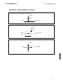
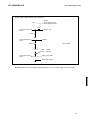
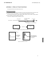
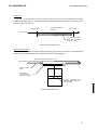
KIT-V850E/MA3-IE
User's Manual (Rev.1.03)
RealTimeEvaluator
KIT-V850E/MA3-IE
User’s Manual (Rev.1.02)
Software Version Up
* The latest RTE for Win32 (Rte4win32) can be down-loaded from following URL.
http://www.midas.co.jp/products/download/english/program/rte4win_32.htm
Notice
* The copyright associated with KIT-V850E/MA3-IE (including software and manual) are proprietary to
Midas Lab. Co., Ltd.
* This software and manual are protected under applicable copyright laws, and may not be copied,
redistributed, or modified in whole or in part, in any way without explicit prior written permission from Midas
Lab. Co., Ltd.
* While this product was manufactured with all possible care, Midas Lab. Co., Ltd. does not guarantee that
this product is free from any problem.
* Midas Lab. Co., Ltd. and its distributor assume no responsibility whatsoever for any result of using this
product.
* The contents and specifications of this software and this manual are subject to change without notice.
Trademarks
* MS-Windows, Windows, MS, and MS-DOS are the trademarks of Microsoft Corporation, U.S.A.
* The names of the programs, systems, CPUs, and other products that appear in this document are usually
trademarks of the manufacturer of the corresponding product.
1
KIT-V850E/MA3-IE
User’s Manual (Rev.1.02)
REVISION HISTORY
Rev.1.00
Jan. 8, 2003
1st edition
Rev.1.01
Feb. 8, 2003
The following modification and addition are made:
* The explanation of SW1 is modified.
* A description related to the setting of the ASID register is
added to "Precautions".
Rev.1.02
Mar. 12, 2003
Clerical error correction
Rev.1.03
Apr. 25, 2003
Clerical error correction
The notation of SW3 and SW4 is reverse at Chapter.4.
2
KIT-V850E/MA3-IE
User’s Manual (Rev.1.02)
CONTENTS
1. OVERVIEW.............................................................................................................................................. 4
2. HARDWARE SPECIFICATIONS ............................................................................................................. 5
3. INSTALLATION PROCEDURE ............................................................................................................... 7
4. SETTING SWITCHES.............................................................................................................................. 8
5. CONNECTING THIS PRODUCT TO THE USER SYSTEM .................................................................... 9
Mounting the EV socket........................................................................................................................... 9
Turning the power on............................................................................................................................... 9
Turning the power off............................................................................................................................... 9
6. RTE for WIN32 ...................................................................................................................................... 10
Invoking ChkRTE2.exe .......................................................................................................................... 10
7. PRECAUTIONS ..................................................................................................................................... 12
Restrictions on CPU emulation.............................................................................................................. 12
Precautions for connecting the user system.......................................................................................... 12
Handling the pod ................................................................................................................................... 12
Settings required for using external bus emulation memory ................................................................. 12
Initializing the ASID register .................................................................................................................. 13
Adjusting supports ................................................................................................................................. 13
External clock input ............................................................................................................................... 13
Caution related to the delay time........................................................................................................... 13
HALT instruction .................................................................................................................................... 13
Breakpoints............................................................................................................................................ 13
Measuring the execution time................................................................................................................ 13
Mounting the CPU on the EV socket ..................................................................................................... 14
Other information................................................................................................................................... 14
APPENDIX A. PACKAGE DRAWING OF THE POD SECTION ............................................................... 15
APPENDIX B. USER INTERFACE CIRCUITS .......................................................................................... 16
APPENDIX C. DETAILS OF TRACE FUNCTIONS ................................................................................... 19
Overview of the trace function ............................................................................................................... 19
Delay count............................................................................................................................................ 20
Trace execution mode ........................................................................................................................... 20
Sub-switch, section, and qualify ............................................................................................................ 21
Starting trace ......................................................................................................................................... 21
Trigger condition.................................................................................................................................... 22
Stopping trace ....................................................................................................................................... 23
Terminating trace................................................................................................................................... 23
Forced delay mode................................................................................................................................ 24
3
KIT-V850E/MA3-IE
User’s Manual (Rev.1.02)
1. OVERVIEW
KIT-V850E/MA3-IE is a kit that performs in-circuit emulation for NEC RISC microprocessor V850E/MA3.
Using a dedicated emulator chip in the kit has made it highly transparent, compact, and lightweight.
Connect the pod to the RTE-2000-TP and use it. Two types of debug monitors are available: Dedicated
PARTNER and GHS Multi.
This product comes with the following items:
1.
V850E/MA3 pod
: 1
2.
RTE for Win32 setup disk
: 1
3.
User's Manual
: 1
4.
Power supply (RTE-PS04: +5 V/4.5 A) : 1
5.
EV socket
: 1 set
6.
Support spacers and screws
: 1 set
In addition to the above items, the following items are required for using this product. They are not
standard accessories.
7.
RTE-2000-TP-x-x
8.
Interface kit (interface card and cable set)
One of the following kits is required:
• PC card interface kit
• PC98 desktop PC interface kit
• DOS/V desktop PC interface kit
• PCI bus interface kit
9.
Debugger
Either of the following debuggers is required:
• Multi debugger
: Multi and Midas server
• PARTNER debugger : PT-V850E1-IE/TP
4
KIT-V850E/MA3-IE
User’s Manual (Rev.1.02)
2. HARDWARE SPECIFICATIONS
Emulation
Target device
V850E/MA3 (TQFP-144)
RTE-TP format to be used
RTE-2000-TP
Emulation functions
Operating frequency
Clock source
Main clock
*4
80 MHz (max.)
Automatic switching between external and internal
clocks (internal: 8 MHz)
Internal ROM emulation capacity
1 MB
Internal RAM emulation capacity
60K bytes (can be switched among 4K, 12K, 28K, and
60K bytes)
External memory emulation capacity
Operation voltage
4M bytes (mounted in the pod section as standard)
3.3 V
Event function
Number of events
Setting of execution address
8
Setting of data access
6
Address specification
Maskable
Data specification
Maskable
Status specification
Maskable
Number of sequential unit stages
Path counter
4
12 bits
Break functions
Hardware breakpoints
Instruction/access breakpoints
2
Address specification
Maskable
Data specification
Maskable
Status specification
Maskable
Software breakpoints
100
Breaks that can be set using events
Supported
Step breaks
Supported
Manual breaks
Supported
External breaks (High/Low edge)
Supported
Trace functions
Trace data bus
48 bits
Trace memory
48 bits × 256k words
Trigger setting
Trigger that can be set using an execution
address
Supported
Trigger setting by data access
Supported
Trigger setting by event
Supported
Trigger setting by external input
Supported
Start/stop specification (sub-switch)
Supported
Trace delay
0 - 3FFFF
Trace clock
Time tag
80 MHz
100 ns - 30 h
Disassembled trace data display function
Provided
Complete trace mode specification function (no
real time)
Provided
5
KIT-V850E/MA3-IE
User’s Manual (Rev.1.02)
ROM emulation functions (*5)
Map function in block (USER/EMEM)
64k words
Used as RAM
Supported
Memory capacity
8M - 128M bytes
Access time ((): burst cycle)
35 ns (30 ns) (*1)
Operation voltage
1.8 - 5 V (*2)
Electrical condition
LV-TTL, 5-V tolerant (*3)
Number of ROMs that can be emulated
DIP-32pin-ROM (8-bit ROM)
4 (max.)
DIP-40/42pin-ROM (16-bit ROM)
4 (max.)
Extend STD-16BIT-ROM connector
4 (max.)
Sizes of ROMs that can be emulated (bits)
DIP-32-ROM (8-bit bus)
1M, 2M, 4M, 8M (27C010/020/040/080)
DIP-40-ROM (16-bit bus)
1M, 2M, 4M (27C1024/2048/4096)
DIP-42-ROM (16-bit bus)
*4
Extend STD-16BIT-ROM (16-bit bus)
8M, 16M (27C8000/16000)
1M, 2M, 4M, 8M, 16M, 32M, 64M, 128M, 256M
(32M bytes)
Bus width specification (bits)
Pin mask functions
8/16/32
NMI, INTWDG, WAIT-, HLDRQ, RESET-
*1, 2, 3: Values when RTE-2000-TP + CBL-STD16-2K is used.
*2: Note that the DC characteristics of each cable may not electrically match when the supply voltage is 2.3
V or less.
*4: External memory emulation (capacity: 4M bytes) occupies one of /CS[0..7] signals and supports a
16-bit bus only.
*5: The user system must have a ROM socket or dedicated connector for connecting the ROM emulation
cable. For details, refer to the manual of the RTE-2000-TP main unit.
Up to four E.MEM boards can be mounted on the RTE-2000-TP, and the maximum capacity is 128M
bytes.
6
KIT-V850E/MA3-IE
User’s Manual (Rev.1.02)
3. INSTALLATION PROCEDURE
Install this product using the following procedure:
1.
Installing the RTE-2000-TP
→ Refer to the manual of the RTE-2000-TP.
2.
Connecting this product to the RTE-2000-TP
→ Connect the pod cable to the CPU-IF connector on the JTAG/N-Wire board module of the
RTE-2000-TP.
3.
Setting switches on the pod
→ See Chapter 4 in this manual.
4.
Connecting this product to a user system
→ See Chapter 5 in this manual.
5.
Installing RTE for Win32
→ Refer to the manual of RTE for Win32.
6.
Initializing RTE for Win32
→ See Chapter 6 in this manual.
7.
Installing the debugger
→ Refer to the manual of the target debugger.
7
KIT-V850E/MA3-IE
User’s Manual (Rev.1.02)
4. SETTING SWITCHES
SW1
Switch for setting the emulation mode
SW1
Symbol
1
CKSEL
Function
2
PSEL
3
SVMODE
4
INTSEL
Initial value
Specifies the status of the CKSEL pin on the CPU when the internal
clock is used.
OFF: High level (through mode), ON: Low level (PLL mode)
ON
Specifies the status of the PSEL pin on the CPU when the internal clock
is used.
OFF: High level, ON: Low level
OFF
Use this switch in the factory-set status.
ON
Specifies the switch mode for the clock supplied to the CPU.
OFF: Auto, ON: Internal clock
OFF
[INTSEL]
Switches the clock supplied to the CPU and related signals (CKSEL and PSEL).
OFF :
When the user system is connected, the signal from the user system is connected.
Otherwise, the internal clock is used.
ON :
The internal clock is always used.
The internal clock frequency is 8 MHz, CKSEL enters the status set by SW1-1, and PSEL
enters the status set by SW1-2.
SW2
Use this switch with all contacts set to OFF because it is not used for this product.
SW3 and SW4
Switches for setting external bus emulation memory.
External bus emulation memory occupies one of eight CS- signals of the V850E/MA3 to map the RAM
mounted in the pod as a hardware component.
Set these switches as follows.
SW4
SW3
CS into which E.MEM
is to be mapped
1
2
3
4
5
6
7
8
1
2
3
4
CS0-
OFF
ON
ON
ON
ON
ON
ON
ON
OFF
OFF
OFF
ON
CS1-
ON
OFF
ON
ON
ON
ON
ON
ON
ON
OFF
OFF
ON
CS2-
ON
ON
OFF
ON
ON
ON
ON
ON
OFF
ON
OFF
ON
CS3-
ON
ON
ON
OFF
ON
ON
ON
ON
ON
ON
OFF
ON
CS4-
ON
ON
ON
ON
OFF
ON
ON
ON
OFF
OFF
ON
ON
CS5-
ON
ON
ON
ON
ON
OFF
ON
ON
ON
OFF
ON
ON
CS6-
ON
ON
ON
ON
ON
ON
OFF
ON
OFF
ON
ON
ON
CS7-
ON
ON
ON
ON
ON
ON
ON
OFF
ON
ON
ON
ON
Not used
ON
ON
ON
ON
ON
ON
ON
ON
x
x
x
OFF
SW1 and SW2 are on the top of the middle board near the end of the pod.
SW3 and SW4 are on the back of the pod.
Do not change the setting of SW0, an eight-contact switch, on the top of the
middle board.
8
KIT-V850E/MA3-IE
User’s Manual (Rev.1.02)
5. CONNECTING THIS PRODUCT TO THE USER SYSTEM
Connect this product to the user system using the following procedure.
Mounting the EV socket
Solder the EV socket supplied with the product on the user system.
Turning the power on
1.
Turn the power to the host personal computer on.
2.
Turn the power to the RTE-2000-TP on.
3.
Turn the power to the V850E/MA3 pod on. (Connect the dedicated power supply to the power
supply jack.)
Confirm that the LED indicating the power status of the pod comes on.
4.
Turn the power to the user system on.
Confirm that the LED indicating the power status of the user system comes on.
5.
Start up the debug monitor.
Turning the power off
1.
Exit the debug monitor.
2.
Turn the power to the user system off.
Confirm that the LED indicating the power status of the user system goes out.
3.
Turn the power to KIT-V850E/MA3-IE off. (Disconnect the dedicated power supply from the power
supply jack.)
4.
Turn the power to the RTE-2000-TP off.
5.
Turn the power to the host personal computer off.
[Caution]
When soldering the EV socket on the board, be careful about the position of pin 1 because the
orientation of the socket is determined. Use the t mark.
The following figure shows how the V850E/xxx pod is connected to the user system.
V850E/xxx pod
To the RTE-2000-TP
Two LEDs
Near LED: Power status of the
pod
Far LED : Power status of the
user system
Power supply jack
Support
703134GJ144-EA
EV socket
Soldering
703134GJ144-TC
User system
9
KIT-V850E/MA3-IE
User’s Manual (Rev.1.02)
6. RTE for WIN32
This chapter describes the setting of RTE for WIN32.
Invoking ChkRTE2.exe
After finishing to connect to the user system and apply the power supply for all equipments, invoke
ChkRTE2.exe to set up the configuration of "RTE for WIN32".
Please set up the "RTE for WIN32" configuration at least one time for newly installed hardware.
<Setting up RTE-products>
<Selecting RTE>
From Product List, select the V850E/MA3-IE located beneath the IE tree.
<Selecting I/F-1, I/F-2>
Select and specify the host interface that suitable for your system from pull-down
menu. (The display in example shows that PCI-Card is assigned.)
V850E/MA3-IE is supported by rte4win32 ver.5.09 or later.
10
KIT-V850E/MA3-IE
User’s Manual (Rev.1.02)
<Function test>
For the function test, RTE for WIN32 must properly be connected to the user system and capable of
debugging. If you set up RTE and then perform a function test according to the screen instructions, the
following dialog box appears upon the normal completion of the test. In this state, control from the
debugger is possible.
Perform the ChkRTE2.exe function test when the power to the user
system is on if it is connected.
If the power is off, an error occurs.
11
KIT-V850E/MA3-IE
User’s Manual (Rev.1.02)
7. PRECAUTIONS
This chapter provides the precautions you should observe when using KIT-V850E/MA3-IE.
Restrictions on CPU emulation
Bit[0,1] of port CT cannot be used as [LBE-,UBE-].
Precautions for connecting the user system
1)
If the power to the user system is turned off in the break status, the ICE puts the CPU into the forced
reset status and stops the output of the signal line to the user system. In this status, the user system
cannot be controlled from the debugger. If you want to turn the power to the user system again, it is
desirable to restart up this system from scratch in principle. To continue with debugging from
necessity, turn the power to the user system on again and be sure to issue the initialize (init)
command from the debugger. Then, set the CPU and debugger again. If the power to the target
system is turned off, then on again after the debugger has started up, however, the debugger may
hang up. In this case, restart up the system from scratch. Do not leave the RTE system with only the
power to the user system turned off because this status may cause a failure in the user system or
this product.
2)
If the CPU in the user system fails to operate normally, the debugger may also fail to start up or hang
up with specific commands.
Handling the pod
The entire circuit of the pod is exposed. Do not allow the circuit to come into contact with metals and
others when it is energized. Otherwise, a failure may occur in the main unit.
Settings required for using external bus emulation memory
The following settings are required:
Port settings:
Port AL : Set this port as addresses in the separate mode.
Port AH : Set A16 to A21 as addresses.
Port DL : Set this port as a data bus.
Port CS : Set CS- for mapping emulation memory to enabled.
Port CT : Set either combination, LWR-/UWR or LBE-/UBE/WR-, to enabled. (The memory
cannot be used with the latter combination currently, however.)
Set RD- to enabled.
Set ASTB to enabled in the multiplex mode.
MEMC settings (setting for the CS- space for mapping emulation memory)
BCTx
: MEn = 1, MMn = Any, BTn[1,0] = [0,0]
DWCx : When the bus clock frequency is less than 33 MHz : One wait state
When the bus clock frequency is 33 MHz or more : Two wait states
LBS
: Set LB0x = 1 (16-bit bus).
12
KIT-V850E/MA3-IE
User’s Manual (Rev.1.02)
Be sure to set port AH so that addresses from A16 to A21 are
enabled. Port AH is directly connected to emulation memory as
addresses. If part of addresses are set as a port, the emulation
memory cannot be accessed correctly.
A user system should not drive a data bus in the state with all
inactive CS signals. It becomes the following causes when driving.
* Injustice of access to an emulation memory
* Failure of a user system or ICE
Initializing the ASID register
Before using the emulator, set the value of the ASID register to 0x00 for future compatibility. If the
emulator is used with the ASID register set to other than 0x00, a break function may be disabled.
Adjusting supports
The pod is designed so that supports can be mounted at its end. Adjust the supports so that the pod
becomes parallel to the board on the user system when it is connected to the user system with the EV
socket.
To adjust the height of a support, loosen the nut and slide the screw
in or out.
After adjusting the height, tighten the nut to fix the screw position.
External clock input
When an external clock is supplied, there are the following restrictions:
* When the clock is input from an oscillator:
Use the clock at frequencies from 5 to 25 MHz.
* When a crystal or another resonator is connected:
Use the clock at frequencies from 4 to 8 MHz. The constant of the external capacitor must be
adjusted according to the resonator individually.
Caution related to the delay time
Almost all signals are connected directly between the CPU in the pod and the user system. However, a
delay of about 3 ns (typical) may occur due to the wiring length to the tip and the capacity, compared with
direct CPU connection. Design the user system with accommodating this delay.
HALT instruction
When a break is made with the HALT instruction, the break address is the starting address of the
instruction next to the HALT instruction.
Breakpoints
If a hardware breakpoint is set to the second instruction of an instruction string that simultaneously
execute two instructions, it is invalid.
Measuring the execution time
The time command displays the execution time from the previous "execution to a break".
The
measurement value contains the overhead time (error of several CPU clocks). Note the following point:
13
KIT-V850E/MA3-IE
User’s Manual (Rev.1.02)
→ If a breakpoint is set at the execution start address, the measurement error is doubled. To measure
the execution time, remove the breakpoint at the execution start address.
Mounting the CPU on the EV socket
Purchase a 703134GJ144-MA, an optionally available component. The 703134GJ144-MA has a socket
for mounting the V850E/MA3 on its top. It can be mounted on the 703134GJ144-TC soldered on the user
system.
Other information
Be sure to refer to the Release Note and other manuals if provided.
14
KIT-V850E/MA3-IE
User’s Manual (Rev.1.02)
77
66.04
30
22
77
APPENDIX A. PACKAGE DRAWING OF THE POD SECTION
1pin
13
GJ144-EA
20
43
99
GJ144-TC
22
69
77
22
Unit: mm
15
KIT-V850E/MA3-IE
User’s Manual (Rev.1.02)
APPENDIX B. USER INTERFACE CIRCUITS
Port 0, Port 1, Port 2, Port 3, Port 4, Port 5, Port 8
TVDD3
100 KΩ
User system
CPU
Port AL, Port AH, Port DL, Port CS, Port CT, Port CD, Port BD
TVDD3
100 KΩ
22 Ω
User system
MEMC
Port
ANI0-ANI7
TVDD3
100 Ω
CPU
User system
16
KIT-V850E/MA3-IE
User’s Manual (Rev.1.02)
RESET-
TVDD3
FPGA
LCX14
100 KΩ
User system
CPU
X1, X2
VHCU04(2/6)
1 MΩ 100 Ω
1 MΩ
X1
User system
100 Ω
CPU
X2
1 MΩ
AVDD0, AVDD1, AVSS
CPU
AVDD
AVSS
+3.3 V
NC.
AVDD
AVSS
User system
17
KIT-V850E/MA3-IE
User’s Manual (Rev.1.02)
CKSEL, PSEL, VDD3, VDD25, VSS, and others
Others
Other VDD3 circuits
Other VDD25 circuits
NC.
1 KΩ
To the level sense
circuit
VDD3 (--pin)
1 KΩ
To the level sense
circuit
CKSEL
100 KΩ
User system
+3.3 V
To the level sense
circuit
VSS : 10 KΩ
PSEL : 100 KΩ
VSS (--pin), PSEL
Other VSS circuits
Remark: TVDD3 is an internal power supply equivalent to a 3.3-V power supply in the user system.
18
KIT-V850E/MA3-IE
User’s Manual (Rev.1.02)
APPENDIX C. DETAILS OF TRACE FUNCTIONS
This appendix describes the real-time trace function.
Overview of the trace function
The real-time trace function writes the details of the execution (trace data) output from the CPU in the
trace buffer in the ICE for each execution. You can check the data using the trace command.
You can set the trace mode, trace start condition, trigger condition, section condition, qualify condition,
and other conditions to specify the loading of trace data.
For the flow of loading trace data, see Figures 1 and 2.
Start of trace
The trigger condition
is satisfied.
End of trace
CPU execution
Data loaded into the ICE
CPU
Trace
Trace data
Figure 1 Flow of loading trace data
End
The trigger
condition is
satisfied.
If the trace buffer in
the ICE becomes full,
it is overwritten from
the beginning.
Start of trace
Figure 2 Trace data in the ICE
19
KIT-V850E/MA3-IE
User’s Manual (Rev.1.02)
Delay count
The delay count means the number of cycles in which trace data is to be loaded after the trigger
condition is satisfied (Figure 3). The number of cycles differs depending on the type of CPU execution. One
cycle is not one execution unit.
Start of trace
The trigger condition is
satisfied.
End of trace
CPU execution
Trace data is loaded
during the specified
number of cycles.
Figure 3 Flow of delay count
Trace execution mode
In the real-time mode, trace data is loaded with priority given to the CPU execution. If the trace buffer
(FIFO) in the CPU becomes full, part of trace data may not be loaded (Figure 4).
When the trace buffer in the CPU is full
CPU execution
Loading of trace
data
The details of
execution during
this section are lost.
Overflow information and
not trace data is written in
the trace buffer.
Figure 4 Real-time mode
20
KIT-V850E/MA3-IE
User’s Manual (Rev.1.02)
In the non-real-time mode, all trace data can be loaded. If the trace buffer (FIFO) in the CPU becomes
full in this mode, the CPU execution is temporarily stopped and is automatically restarted (Figure 5).
The CPU is temporarily
stopped.
The CPU is restarted.
CPU execution
Loading of trace
data
Trace data is not loaded
when the CPU is
temporarily stopped.
Figure 5 Non-real-time mode
Sub-switch, section, and qualify
The sub-switch indicates whether OR or AND (set by tenv [subor|suband]) of the section and qualify
conditions are satisfied (on) or not (off). You can specify cycles in which trace data is to be loaded according
to the on or off status (sswon/sswoff command). By specifying cycles in which trace data is to be loaded for
sswon and nothing to be loaded for sswoff, the on/off status of this sub-switch corresponds to the start or
stop of trace. (The initial value of the sswon/sswoff command is as described above. In the description
below, these commands are assumed to be set to their initial value.)
You can specify a section using the tsp1 and tsp2 commands and evt secon and secoff parameters. Use
tsp1 and secon to specify that a section is established (on) and tsp2 and secoff to specify that a section is
not established (off).
The event condition specified for qualify in the evt command is used as a qualify condition. When the
event condition is satisfied, the qualify condition is also satisfied.
Starting trace
To start loading trace data, the following methods are available: Forced start method (tron force) and the
method using the status of the sub-switch according to the section and qualify setting. (Figure 6)
To set the loading condition using the sub-switch, use sswon and sswoff. Usually, specify cycles in
which trace data is to be loaded for sswon and nothing to be loaded for sswoff. According to this setting,
trace data is loaded in the sub-switch on state and the loading of trace data is stopped in the sub-switch off
state.
21
KIT-V850E/MA3-IE
User’s Manual (Rev.1.02)
• Start unconditionally loading trace data (tron force)
• Set section point (tsp1, evt secon)
• Set qualify (evt qualify)
The condition
is satisfied.
Start of trace
CPU execution
Loading of trace
data
Figure 6 Starting trace
Trigger condition
A trigger condition is used as the start point of delay count (Figure 7). You can set a trigger condition to
check the details of the execution before and after the trigger.
• The instruction at the trigger address (tp) is executed or trace data
(td1, td2, td3, or td4) is accessed.
• The external signal condition is as specified (tron noext|posi|nega).
• The event match point factor is established (evt match).
The condition
is satisfied.
The trigger condition
is satisfied.
End of trace
CPU execution
Execution is traced during
as many cycles as the delay
count and trace is forcibly
terminated.
Figure 7 Trigger condition
22
KIT-V850E/MA3-IE
User’s Manual (Rev.1.02)
Stopping trace
To stop loading trace data, use the status of the sub-switch according to the section and qualify setting.
(Figure 8)
To set the loading condition using the sub-switch, use sswon and sswoff. Usually, specify cycles in
which trace data is to be loaded for sswon and nothing to be loaded for sswoff. According to this setting,
trace data is loaded in the sub-switch on state and the loading of trace data is stopped in the sub-switch off
state.
• Set section point (tsp2, evt secoff)
• Set qualify (evt qualify)
The condition
is satisfied.
Stop of trace
Start of trace
Stop of trace
CPU execution
Loading of trace
data
Loading of trace
data
Figure 8 Stopping trace
Terminating trace
After trace is terminated, no more trace data is loaded.
When the end condition is satisfied, unlike the stop condition, trace is not restarted (Figure 9).
• Stop CPU execution.
• Forcibly terminate trace (troff).
• End delay count.
The condition
is satisfied.
Start of trace
End of trace
CPU execution
No more data is loaded.
Loading of trace
data
Figure 9 Terminating trace
23
KIT-V850E/MA3-IE
User’s Manual (Rev.1.02)
Forced delay mode
In the forced delay mode, trace is forcibly terminated when trace data is loaded during the specified
delay count (number of cycles) after the start of trace. In this mode, the trigger condition is ignored (Figure
10).
When CPU execution starts, trace is started in this mode.
Start of trace
End of trace
CPU execution
Trace terminates after trace
data is loaded during as many
cycles as the delay count.
Figure 10 Forced delay mode
24