1
AD27uD|ADA2700
User'sManual
Real Time Devices,fnc.
"Accessing
theAnalogWorld'k
AD2700/ADA2700
UsertsManual
ffi
REALTIMEDEVICES,
INC.
820NorthUniversity
Drive
PostO,fficeBox906
StateCollege,Pennsytvania
16804USA
Phone:(814)234-8087
FAX:(81a)234-5218
Pubtishedby
RealTime Devices,Inc.
820N. UniversityDr.
P.O.Box 906
StateCollege,PA 16804USA
Copyright @ l9Y2 by Real Time Devices,Inc.
All rights reserved
Printedin U.S.A.
Rev.G 9310
Thbleof Contents
INTRODUCTION......
Digital-to-Analog
(AnA2700Only)...........
Conversion
..........................r-3
WhatComes
ApplicationsSoftwareandToolkit
FlardwareAccessories
CHAPTER 1 - BOARD SETTINGS
............i4
1-l
Factory-Configured
SwitchandJumperSettings
...............1-3
P3- AnalogInputVoltageRange(FactorySetting:10Vols)......
.......................1_3
P4- AnalogInputVoltagePolariry(FacorySering: +/-) ..............
.....................1_3
P5 - DMA RequesrChannel(FactorySetting:Disabled).....
...........l-4
P6 - DMA AcknowledgeChannel(FactorySeuing:Disabled)
......l_5
n-8254TimerlCounterClockSources(FacorySeuings:
CLKI-OSC,CLK2-OTI,PCK)......................1-5
P8 - IntemrptSourceandChannel(FactorySetting:Jumperson OT2 & G; IntemrptChsDisabled).........l-6
P10- DAC I OutputVoltageRange@actorySering:+5 o -5 volts)............
......1-7
Pl1 - DAC 2 OurputVolageRange(FactorySening:+5 o -5 volrs)............
......1_g
P13- Single-EndedlDifferenrial
AnalogInputs(FactorySeuing: single-Ended)
....................1-g
P14- ND ConvefterSatuqlExtern
al Gate2 Monitor@actorySetting:EOC (A/D ConverterSanrs))........l-9
Pl5 - AID DataWordBir SrateSet(FactorySening:+/-) ..............
......................1-9
Sl - BaseAddress(FactorySetting:300hex(768decimal) .................
..............1_9
52 - BufferBypassSwitch(FacorySering:OPEN(Not Bypassed))
...................
..................1_10
Pull-up/Pull-down
Resistorson Digital VO Lines.....
.......l_ I I
CHAPTER 2 - BOARD INSTALLATION
Connecting
theAnalogInputPins
ConnectingttreTriggerIn andTriggerOut Pins,Cascading
Boards.........
Connecting
theAnalogOutputs(ADA2700Only)...........
Connecring
theTimer/Counters
andDigiralVO...............
Runningthe2700DIAGDiagnostics
Program
CHAPTER 3 _ HARDWARE DESCRIPTION
D/A Converte
............24
..............2_6
..................2_6
..................2-6
...................2_6
3-l
Digital I/O, Programmable
PeripheralInterface
CHAPTER 4 _ BOARD OPERATION AND PROGRAMMING
BA + 0: ReadData/StartConverr(Read/Write)
BA + 2: ReadStatus/Reset
(Read/Wrire)
................
BA + 4: ChanneVGain/Board
FuncrionsSelecr(ReadAMrite)
BA + 8: D/A ConverterI (ADA2700DACI) (WriteOnly)...........
BA+ 10: D/AConverter
2( Dlo7n DAC2)(Writeonly)...........
BA + 16: PPIPortA - Digial VO (Readl'\ilrite)
................
BA + 18: PPIPortB - DigitalVO (ReadAMrire)
.............
BA + 20:PPIPortC - DigiralVO Eead/Wrire)................
BA+22: 8255PPIConnolWod (WriteOnly) ...........
BA+24: 8254Timer/CounrerO
(ReadflMrite)
BA + 26: 8254Timer/Counter1 (ReadflMrite)
BA + 28: 8254Timer/Counter2 (ReadflMrire)
BA + 30: 8254Conrol Word (WriteOnly)...........
ClearingandSettingBirsin a Port..........
EnablingandDisablingtheExternalTrigger
Enabling
andDisabling
RQ..........
Conversion
Modes/Triggering
............
Startingan A/D Conversion
MonitoringConversion
Status(DM.l Doneor End-of-Convert)
ReadingtheConverted
Data............
Programming
thePacerClock..........
.................3-5
4-l
............44
......44
...........4_5
........................4_5
......................4-5
.............4_6
................4_6
..............4_6
.....................4-6
.............4_g
.............4_8
.............4-g
.......4_g
.......................4_9
..........4-il
.....4_tl
.....................4_l
l
................4-lz
......................4_lz
...4_I3
.......................4_14
What Is
8259hogrammableIntemrptControllers
InterruptMaskRegisters(IMR)
End-of-IntemrptGOf) Command
WhatExactlyllappensWhenan IntemrptOccurs?
UsingIntemrptsin Your Programs
Writingan IntemrptServiceRourine0SR)...........
Savingthe SarnrpIntemrptMaskRegister(IMR) andIntemrptVecor
Restoringthe StartupIMR andIntemrptVector
CommonIntemrptMisakes
Choosinga DMA Channel
Allocatinga DMA Buffer
Calculating
thePageandOffsetof a Buffer
SettingtheDMA PageRegister...................
TheDMA
...............4_15
..........4-15
......4_16
.....................4_16
.....4_16
.......................4-16
..........4_17
.....4-lg
...............4_lg
..................4_19
...................4_19
............4_19
............4_Zl
APPENDIX C _ COMPONENTDATA SHEETS
APPENDIX D _ CONFIGURINGTHE 27OO
FOR SIGNAL*MATH
APPENDIX E _ CONFIGURINGTHE 27OO
FOR ATLANTIS........
APPENDIX F _ WARRANTY
tu
......D.1
.................E-l
TV
LIST OF ILLUSTRATIONS
1-l
r-2
1-3
t4
l-5
1-6
r-7
1-8
r-9
1-10
l - 11
l-t2
l-r3
t-14
r-15
1-16
r-t7
l-18
l-19
r-20
2-r
)-)
2-3
24
3-1
3-2
4-l
4-2
+-1
44
4-5
4-6
+-t
5-l
BoardLayoutShowingFactory-Configured
Settings
AnalogInputVoltageRangeJumper,P3
AnalogInputVoltagePolarityJumper,p4 ................
DMA Request
ChannelJumper,P5 ................
DMA Acknowledge
ChannelJumper,P6................
p7................
8254Timer/Counter
ClockSourceJumpers,
8254Timer/CounterCircuit Block Diagram
IntemrptChannelJumper,P8 ................
Pulling Down theIntemrptRequestLine
DAC I Ouput VoltageRangeJumper,p10 ..............
DAC 2 OutputVolrageRangeJumper,Pl I ..............
pt3 ..........
Single-Ended/Differendal
AnalogInputSignalTypeJumpers,
A/D Converter
Status/External
Gate2 MonitorJumper,p14....
A/D Daa WordBit StateSetJumper,Pl5
BaseAddress
Switch,Sl ...............
PortC BufferCircuiry ...............
Pull-uplPull-down
Resisror
Circuitry......
AddingPull-upsandPull-downsto DigitalVO Lines
GainCircuiry andFormulasfor Calculating
Gm andf ...................
Diagramfor Removalof SolderShort...........
pin Assignments
n IlO Connector
andPl2 On-board
Connector
.................
Single-Ended
InputConnections
............
DifferentialInputConnections
............
Cascading
Two Boardsfor SimulaneousSampling
AD?7W|ADA27JI_BlockDiagram
8214Timer/Counrer
Circuit Block Diagram
A/D ConversionTiming Diagram,All Modes....
PacerClockBlockDiagram
8Zl4Timer/CounrerCircuit Block Diagram
SingleConversion
Flow Diagram
DMA Flow Diagram
IntemrptsFlow Diagram
D/A ConversionFlow Diagram
................14
.............1-3
................1-4
.....t4
..................1_5
........1-5
........l_6
...............
l_6
.............1_7
................1-g
................
l_g
.........................1_g
.....................
l_9
...........1_9
.....................1_10
...l-11
............1_12
.............1_13
............1_14
.....l_14
....................24
..............2_5
.................2_5
..,,.............2_6
.....................3_3
........34
.....................4-12
...........4_14
......4_24
.......................4-27
......................4-Zg
................4_2g
.....4_30
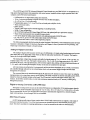
INTRODUCTION
The AD2700andADA2700AdvancedIndusrial Controlboardsturn your IBMo PC/AT or compatibleinro a
high-speed,
high-performance
dataacquisitionandcontrolsystem.Installedwithin a singleexpansionslot in the
computer,each27ffi seriesboardfeatures:
. 8 differentialor l6 single-ended
analoginputchannels,
' 12-bit,5 microsecond
analog-to-digital
converter
with 150kHz throughput,
. *5, *10, or 0 to +10volt inputrange,
' Programmable
gainsof 1,2,4, and8 with anon-boardgainmultipliercircuit,
. Threeconversionmodes,
. DMA transfer,
. Triggerin andrigger out for extemaltriggeringor cascading
boards,
. 16-birAT buscompatibiliry,
' 24 TTLICMOSbuffered8255-based
digitalI/O lineswith optionalpull-upor pull-downresistors,
. Threel6-bit timer/counters
(two cascaded
for pacerclock),
' Two l2-bit digital-o-analogoutputchannelswith dedicared
grounds(ADA2700only),
. t5, +10,0 to +5, or 0 to +10 volt analogoutputrange(ADA2Z00
only),
. TurboPascalandTurboC sourcecode;diagnostics
program.
The following paragraphs
briefly describethemajorfunctionsof theboard.A moredetaileddiscussionof board
functionsis includedin Chapter3, HardwareOperation,andChapter4, Board Operationandprogramming.
The
boardsetupis described
in Chaprerl, Board Settings.
Analog-to-DigitalConversion
(A/D) circuitryreceivesup to 8 differentialor 16single-ended
analoginputsandconverts
. The analog-to-digital
theseinputs into l2'bit dtgital datawordswhich can thenbe read and/ortransferredto pC memory.
The boardis
facmryserfor single-ended
input channels.
Theanaloginput voltagerangeis jumper-selectable
for bipolarrangesof -5 o +5 volts or -10 ro +10 volts,or a
unipolarrangeof 0 to +10 volts.The boardis factorysetfor -5 to +5 voln. Overvoltageprotectionto +35 volts
is
providedat theinpuB.The high-performance
A/D convertersupportsfast-settling,
soit*.-p.grammable gainsof
l'2,4, and8 with on-boardgainmultipliercircuitryso thatyou cancustomizettri inputgain.
A/D conversions
areperformedin 5 microseconds,
andthe maximumthroughputrateis 150kHz. Conversions
arecontrolledttrroughsoftware,by an on-boardpacerclock, or by an externaltrigger broughtonto the
board
throughtheI/O connector.
Theconverteddatacanbe ransfenedthroughthePCdatabusto PC memoryin oneof two ways:
by usingthe
microprocessor
or by usingdirectmemoryaccess@MA). The modeof transferis software-selectable
andthe DMA
channelis chosenby jumpersettingson theboard.ThePC databusis usedto readand/ortransferdata pC
o
memory.In theDMA Fansfermode,you canmakecontinuoustransfersdirectlyto pC memorywithoutgoing
throughtheprocessor.
Digitaf-fo-AnalogConversio
n (AD A2700Onty)
The digital-to-analog
(D/A) circuitryon theADA2700featurestwo independent
l2-bir analogoutputchannels
with individuallyjumper-selectable
outputrangesof -5 to +5 volts,-10o +10volts,0 to +5 volts,or 0 to +10 vols.
Datais programmedinto theD/A converteranda conversionis automaticallytriggeredfor a channel
througha
singlewriteoperation.
AccessthroughDMA is not available.
8254Timer/Counter
An 8254programmable
intervaltimercontainsthreel6_bit,g_MHztimer/counters
to supporta wide rangeof
timing andcountingfunctions.Two of thetimer/counters
arecascaded
andcanbe usedinternaly for thepacJr
clock.The third is availablefor countingapplications,
or it canbe cascaded
to theothertwo timer/counters.
i-3
DigitalVO
The 2700has24TlL/CMOS-compadbledigitalI/O lineswhichcanbe directlyinterfacedwith exrernaldevices
or signalsto senseswitchclosures,triggerdigital evens,or activatesolid-staterelays.Theselinesareprovidedby
theon-board8255programmable
peripheralinterfacechip.The 8255canbe operatedin oneof t*o modes:Mod;0
or Mode l. To ensurehigh driving capacity,CMOSbuffersareinstalled.TTL buffersareavailableon request.
Padsfor installingandacdvatingpull-upor pull-downresistorsareincludedon theboard.Installationproceduresaregivenneartheendof ChapterI, Board Settings.
What ComesWith Your Board
You receivethefollowing itemsin your 2700package:
. AD2700or ADA2700inrerfaceboard
' Softwareanddiagnosticsdiskettewith TurboPascalandTurboC source
code
. User'smanual
If any item is missingor damaged,
pleasecall RealTime Devices'CustomerServiceDepartmentat
(814) 234'8087.If you requireserviceouside theU.S.,contactyour local distriburor.
Board Accessories
In additionto theitemsincludedin your 2700package,
RealTime Devicesoffersa full line of softwareand
hardwareaccessories.
Call your local distributoror our mainoffice for moreinformationabouttheseaccessories
and
for help in choosingthebestitemsto supportyourboard'sapplication.
ApplicationSoftwareand Drivers
Our customapplicationsoftwarepackages
provideexcellentdataacquisitionandanalysissupport.Use
SIGNAL*MATH for integrateddataacquisitionandsophisticated
digital signalprocessingandanalysis,or
ATLANTIS for real-timemoniloringanddataacquisition.rtdlinx andrtdlinxlablinx driversprovidefull-featured
high level interfacesbetweenthe2700andcustomor third partysoftware,includingLABTECH NOTEBOOK,
NOTEBOOKIKE,andLTICONTROL.rtdlinx sourcecodeis availablefor a one-timefee.Our pascalandC
Programmer's
Toolkit providesroutineswith documented
sourcecodefor customprogramming.
HardwareAccessories
Hardwareaccessories
for the2700includerheMX32 analoginput expansionboardwhich canexpanda single
input channelon your 2700to 16differentialor 32 single-ended
inputchannels,MR seriesmechanicalrelayoutput
boards,OP seriesoptoisolated
digital inputboards,theTS16temperature
sensorboard,theTB50 terminalboardand
XB50 prototype/terminal
boardfor easysignalaccessandprotorypedevelopment,
rheEX-XT andEX-AT extender
boardsfor simplifiedtestinganddebuggingof prototypecircuitry,andXT50 twistedpair wire flat ribboncable
assemblyfor externalinterfacing.
UsingThis Manual
This manualis intendedto helpyou installyour newboardandget it runningquickly, while alsopr,oviding
enoughdetailabouttheboardandis functionsso thatyou canenjoymaximumuseof ils featuresevenin themost
complexapplications.We assumethatyou alreadyhavean understanding
of dataacquisitionprinciplesandthatyou
cancustomizetheexamplesoftwareor write your own applicationsprograms.
When You NeedHelp
This manualandtheexampleprogramsin thesoftwarepackageincludedwith your boardprovideenough
informationto properlyuseall of ttreboard'sfeatures.If you haveanyproblemsinstallingor usingrhisboard,
contactour TechnicalSupportDepartrnent,
(814)234-8087,duringregularbusinesshours,easternstandardtime or
easterndaylighttime,or senda FAX requestingassistance
to (814)234-5218.Whensendinga FAX request,please
includeyourcompany'snameandaddress,
yourname,yourtelephone
number,anda briefdescription
of ne
problem.
,1
CHAPTER 1
BOARDSETTINGS
The AD2700andADA2700boardshavejumperandswitch
settingsyou canchangeif necessary
for your application.The
2700is factory-configured
with themostoftenusedsettings.The
factorysettingsarelistedandshownon a diagramin the beginning
of this chapter.shouldyou needto changethesesettings,usethese
easy-to-followinstructionsbeforeyou installthe boardin your
computer.
NotethatDIP switch52 is providedto bypasstheport C
buffersandallow Mode I operationof the8255.Also notethat by
installingresistorpacksat the four locations,andsolderingjumpersin thedesiredlocationsin the associated
pads,you canconfigure your digital VO linesto bepulledup or pulleddown.This
procedureis explainedneartheendof this chapter.
By installingcomponents
ar Rl, R2, TR4, andC46,you can
addyour own gainmultiplierto the softwareprogammablebinary
gainsof t,2,4, and8. Thegainmultipliercircuioryis described
at
theendof this chapter.
1-l
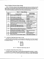
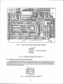
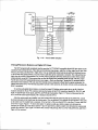
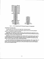
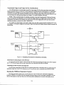
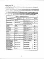
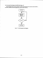
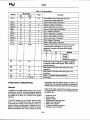
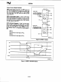
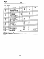
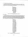
Factory-Configured Switch and Jumper Settings
Table1-1lisc thefacory settingsof theuser-configurable
jumpersandswirchon theAD2700and ADA27ffi
boards.Figure1-1(onthenextpage)showstheboardlayoutandthelocationsof thefactory-set
jumpers.The
followingparagraphs
explainhowto changethefactorysenings.
Payspecialauentionto thesettingof Sl, thebase
address
switch,to avoidaddress
contention
whenyoufirst useyourboardin yoursystem.
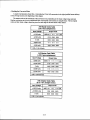
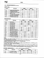
Table1.1- FactorySetilngs
Swltch/
Jumper
Faclory settlngs
(JumpersInstalled)
10 vohs
Bipolar(-5to +5 vohs)
(mustbe the sameas P15)
P3
FunctlonControlled
Setsthe analoginputvoltagerange
P4
Setsthe analoginputvoltagepolarity
P5
P8
P10
Setsthe DMArequest(DRQ)channel
Disabled
Setsths DMAacknowledge
(DACK)channel
Disabled
Setslhe clocksourcesfor the 8254timer/counters Jumpersinstalled
on CLK1-OSC,
TC1out (PCK)to A/Dtrigger
CLK2OT1,& PCK
OCO-TC2);@nnects
Conneclsoneof fourinterrupt
sourcssto an interrupt Jumpersinstall€d
on G (ground
channel;pullstri-statebufferto ground(G)for multiple for buffer)& OT2;interrupt
interruptapplications
channelsdisabled
Setsthe D/Aoutputvoltagerangefor DAC1
+5 to -5 volts
P11
Setsthe D/Aoutputvohagerangefor DAC2
P13
s'l
Sglectssingle-ended
or diffErential
analoginputtype
Seledsihe A/D converterstalusor the externalgate
of timer/counter
2 to be available
lor monitoring
Setsthe stateof thEtop 4 bits(thebitsnot usedby
lhe 12-bitconverter)
of the 16-bitAy'Doutputword
Setsthe baseaddress
EOC(A/DconvsrtErstatus)
Bipolar
(mustbe the sameas P4)
300hex(768decimal)
S2
Bypasses8255PortC buffersfor Mode1 operation
Open(buffersnot bypassed)
P6
P7
P14
P1s
+5 to -5 volts
(jumpersinstalted
Single-ended
on thresSE pins)
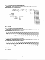
P3 - Analog Input VoltageRange(Factory Setting: 10 Volts)
This headerconnector,shownin Figurel-2, setsilre analoginput volage rangefor l0 or 20 volts.Notethatif
thejumperis insalled on 20V, thenP4 canonly be setfor bipolu (+t-).Theinputrangesallowedby the2700are
15, +10,and0 to +10 volts.
P3
20V 10V
Fig. 1-2- AnalogInputVoltageRangeJumper,p3
P4 - Analog Input VoltagePolarity (Factory Setting: +/-)
This headerconnector,shownin Figure1-3,setstre analoginput volage polarityfor unipolar(+) or bipolar
(+/-). If thejumperon P3 is installedon 20V, thenP4 canonly be setfor bipolar(+/-). The inputrangesallowedby
the2700are15, +10, and0 to +10 volts.NOTE: P4 and P15must be set the samefor proper board operation.
1-3
#ffiHE$EgHFJ
ooo
trrALT-l
pffiffilE#H
EOO
o
'lffi3Elooo
'il3:llEl
iI
lool*ol
".te9"ol
o
o
Io
Io
6E-E
oooo
ooo000
otrr oo
OOra OO
oooooo
oooo
otr l.gl
oooooo
OFIT-4I6TTE
oK)ooolloOOol
& tr:a
A-ooo_oo-ooooo.
Hfu#
r
E tr:r
ch
t
*$RN6
i
E
o
6
:-f o
i
oooooo
oooooooo o
oo
oo o
ogr
oo o
O0 azcss OO
o
oo
00
t
H
5
o0000000
t
8
oooooo
P
€
oooooooooo
@;.
6 S
n d fiDr
lhrykr,
h€. sbtr
Eg
Colhgo, P. t6!Oa tJgA
Fig.1-1- BoardLayoutShowingFaclory-Conligured
Sefiings
+ +l-
P4
Sot P15to the samepolarity!
Fig. 1-3 -Analog lnput Voltage PolarityJumper, P4
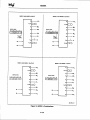
P5 - DMA RequestChannel@actorySetting: Di.sabled)
This headerconn@tor,shownin Figure1-4,letsyou selectchannel5,6, or 7 for DMA Eansfers.This line, the
DMA requestline (DRQ), must be set to the sarnechannelas rheDACK line on K. The frclr:rrysettingis DMA
disabled.Note that if any other devicein your systemis alreadyusingyour selectedDMA channel,channelcontenrion will result, causingerraticoperation.
P5
3i.;Et
Fig.1-4- DMARequest
ChannelJumper,
P5
t4
P6 - DMA AcknowtedgeChannet(FactorySetting: Disabled)
This headerconnector,shownin Figure1-5,letsyou selectchannel5, 6, or 7 for DMA Eansfers.This line,
the
DMA acknowledge
line (DACK), mustbe setto thesamechannelasrie DRe line on p5. Thefactoryseftingis
DMA disabled.Note thatif anyotherdevicein your systemis alreadyusingyour selectedDMA channel,
channel
contentionwill result,causingerraticoperation.
P6
3ilfHt
Fig. 1-5 -
DMA AcknowledgeChannelJumper,p6
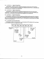
P7 -8254 Timer/CounterClockSources(FactorySettings:CLKI-OSC, CLK2-OT1,pCK)
This headerconnector,shownin Figurel-6, letsyou selecttheclocksourcesfor the8254timer/counters,
TC0,
TCI' andTC2.TCOandTCI arecascaded
to form thepacerclock.You mustinstalltwo or threejumpersin orderto
properlyusethetimer/counterfeatures,includingthepacerclock.Figure l-7 showsa block diagram
of ttretimer/
countercircuitry to helpyou in makingtheseconnections.
The clock sourcefor TCOandTCI is selectedby placinga jumperon OSCor ECl on CLKI (thetwo pairs
of
pins at the op of the header)'oSC is theon-board8-MHz clock andECI is an extemalclock sourceyou
connect
throughtheexrernalI/O connector(p245).
Below theCLKI pinsarethreepairsof pinslabeledCLK2.Thesepins areusedto selecttheclock sourcefor
TC2' OTI connectstheoutputof TCI to theclockpin of TC2. Installinga jumperherecascades
a1 threetimer/
counters,a featurenecessary
whenusingSIGNAL*MATH or ATLANTIS sofnrare(seeAppendixesD andE).
OSCis theon-boardS-MHzclock,andEC2 is connecred
ro thesameexternalclock sourceasECI (p245).
The lasttwo pins on this header,PCK andET, let you usethepacerclock (pCK) or an extemaltrigger(ET)
ro
triggerA/D conversions.
A jumpermustbe placedon PCK in orderto usefte pacerclock (outputrro* iCry. cir,
you canplacethejumperacrossET andconnectanyexternaltriggertoY2-39to triggertheA/b convener.
NOTES: You mustdisconnectthepacerclockby removingthePCKjumperandinstallthejumperof ET
wheneveryou usetheextemaltriggerline. You musthaveonejumperinstalledon oneof the two CLKI selections
andonejumper insralledon oneof thethreeCLK2 selections.
P7
osc
Y
EC1
oTl
o
6l
osc
Y
o
EC2
PCK
ET
p7
Fig.1-6-8254 Timer/Counter
ClockSource
Jumpers,
l-5
2700
I/O CONNECTOR
P2
TO A/D
TRIGGER
P7
CLKI
)
o--
I
I
I
8 MHz
EXTCLK
EXT GATE1
PrN39lrRtGGER tN
TiC OUT 1
Fig. 1-7 -
8254 Timer/CounterCircuitBlock Diagram
P8 - Interrupt Sourceand Channel (FactorySetting: Jumperson OT2 & G; Interrupt ChannelsDisabled)
This headerconnector,shownin Figure1-8,letsyou connect,
anyoneof thefour intemrptsoruceso anyof I I
intemrptchannels,IRQg (highestpriority channel)ttrroughIRQI2, IRQ14,IRQ15,and thenbackto IRe3 through
P8
Fig.1-8a:
FactorySetting
P8
oT2
oT2
ET
ET
EOC
EOC
DMA
IRQ3
Fig.1-8b:Interrupt
Source
Connected
to lRQ3
DMA
IRQ3
IRQ4
IRQ4
IRQ5
IRQS
IRQ6
IRQ6
IRQT
IRQT
IRQ9
IRQg
IRQlO
IRQlO
IRQl1
IRQl1
IRQ12
IRQl2
IBQ14
tRo14
IRQ15
G
IRQl5
G
Fig.1-B- lnterrupt
ChannelJumper,
l-6
IRQT (lowestpriority). Chapter4 explainsintemrpt channelprioritization in deail. To activatea channel,you
must
install a jumper horizontallyacrossthe desiredIRQ channel.Figure l-8a showsrhefactory serring;figurei-gb
showsthe intemlpt sourceconnectedto IRe3.
At the top of the header,you can selectany oneof four signalsourcesto generatean intemrpt. An intemrpt
sourc'eis chosenby placinga jumper acrossthe desiredpair of pins. The intenupt sourcesavailable
are the ttre
outputof timer/countn 2 (oT2), extemalrigger (ED, elo end-of-convert
@OC),and DMA done(DMA).
when jumpered'the bottompair of pins on P8, labeledG, connectsa I kilohm pull-down resistor
to the output
of a high-impedancetri-statedriver which carriesthe intemrptrequestsignal.This jul-down resistor
drives the
intemrpt requestline low wheneverintemrptsarenot active.Wheneveran intemrpi requestis
made,the ti-state
buffer is enabled,forcing the ouput high and generatingan intemrpt You can monioithe intemrpt
sa6s through
bitz n the sE[us word (I/O addresslocationBA + 2). After the inrcmrpt hasbeenserviced,thereset
command
retumsthe IRQ line low, disablingthe ri-state buffer, andpulling ttreouput low again. Figure
l-9 showsthis
circuit Becausethe intemrpt requestline is driven low only by G pull-down resis6r, you i* have
two or more
boardswhich sharethe sameIRQ channel.You cantell which boardissuedthe intenuit request
by monitoringeach
board'sIRQ sanrsbit.
NOTE: When you usemultiple boardsthat sharethe sameinremrpt,only oneboardshould
havethe G jumper
installed.The rest shouldbe disconnected.
Wheneveryou operatea singteboard,lhe G jumper shouldbe insalled-
INT
SOURCE
IRQ STATUS
INTERRUPT
Fig. 1-9 -
PultingDown the InterruptRequestLine
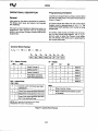
P10- DAc I output voltage Range(Factory setting: +s to.5 vorts)
This headerconnector,shownin Figurel-10, setstheoutputvoltagerangefonDAC I at 0 +5,
1p t5, 0 to +10,
o1t10 volts.Two jumpersmustbe installed,oneto selecttheiangeani one!o selectthemultiplier.The
two
rightmostjumpersselectthe range,brpolar(t5) or unipolar (5). The t*o leftmostjumpersselect
the multiplier, X2
or Xl. Whena jumperis on the X2 multiplierpins,therangevaluesbecome+10 and 10.The rable
belowshowsthe
four possiblecombinationsof jumper settings,and the diagramshowsthet5 volt bipolar setring.
This headerdoes
not haveto be setthesameasPl l.
Jumpers(Leftto Rlghr)
VoltageRange
x2
xl
*5
5
-5 to +5 vohs
OFF
ON
ON
OFF
0 to +5 volts
OFF
ON
OFF
ON
-10lo +10volts
ON
OFF
ON
OFF
0 lo +10 volts
ON
OFF
OFF
ON
t-7
PlO DAC1
:II:
x2x1r5 5
Fig. 1-10Pll-
DAC 1 OutputVoltageRangeJumper,P10
DAC 2 Output VoltageRange(Factory Setting:+5 to -5 votts)
This headerconneclor,shownin Figure1-11,ses theoutputvoltagerangefor DAC 2 at 0 !o +5, t5, 0 to +10,
or +10 volts. Two jumpersmustbe installed,one!o selectthe rangeandone o selectthe multiplier. The nvo
rightmostjumpers selectthe range,bipolar (+5) or unipolar (5). The two leftmostjumpers selectthe multiplier, X2
or Xl. When a jumper is on the X2 multiplier pins, the rangevaluesbecome+10 and 10.The tablebelow showsthe
four possiblecombinationsof jumper settings,andthe diagramshowsthe+5 volt bipolar seuing.This headerdoes
not haveto be setthe sameasP10.
Jumpers(Leftto Rlght)
VoltageRange
and Polarhy
x2
x1
r5
5
-5 to +5 vohs
OFF
ON
ON
OFF
0 to +5 vohs
OFF
ON
OFF
ON
-10lo +10vohs
ON
OFF
ON
OFF
0lo +10volts
ON
OFF
OFF
ON
Pll DAC2
:II:
x2x1r5 5
Fig. 1-11-
DAC 2 OutputVoltageRangeJumper,P11
P13- Single-Ended/DifferentialAnalog Inputs (Factory Setting: Single.Ended)
This headerconnector,shownin Figure 1-12,configuresttre2700 for 8 differentiat or 16 single-endedanalog
input channels.Whenoperatingin the single-endedmode,threejumpersmusrbe inse[ed acrossthe SE pins. When
operatingin the differential mode,two jumpersmust be installedacrossthe D pins. DO NOT insall jumpersacross
bottrSE andD pinsat thesametime!
EI
U'
a
uJ
U,
E
o
uJ
o
P13
Fig.1-12- Single-Ended/DifferentialAnalog
lnputSignalType
Jumpers,P13
1-8
P14- A,/DConverterStatudExternal Gate 2 Monitor (FactorySetting: EOC (A/D ConverterStatus))
This headerconnector,shownin Figurel-13, letsyou selecteitherthe A,/Dconverterstatusor theexternalgate
input of timer/counter2 to be availablefor monitoringat bit 3 of the statusword (BA + 2). The A/D converter
status
providesa directreadof the A/D converter'savailabilityfor sarting conversions.
This line goeslow whena
conversionstarts,thengoeshigh whentheconversionis completed.Chapter4 providesa ror" detailedexplanation
of this statussignal.
Pl4
l-l
'c,
I o.< leoc
Fig. 1-13 - A/D ConverterStatuyExternalGate 2 MonitorJumper, p14
P15- A/D Data Word Bit StateSet(Factory Setting: +/-)
This headerconn@tor,shownin Figurel-14, setsthe stateof theunusedfour bis in the l6-bit A/D daraword.
This headerensuresthat thesefour topmostbits are setat 0 for unipolarconversionsandat the samestateas
the
MSB of the 12-bitA/D converteddatafor bipolarconversions.
Chapter4, BA + 0, explainsthis in moredeail.
NOTE: P15and P4 must be set the samefor proper board operation.
Set P4 to the samepolarityl
Fig. 1-14 -A/D Data Word Bit State Set Jumper, p15
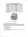
51-
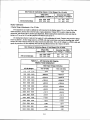
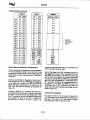
BaseAddress(FactorySetting:300hex (76Edecimal))
Oneof themostcommoncausesof failurewhenyou arefirst trying your boardis addresscontention.Someof
your computer'sI/O spaceis alreadyoccupiedby internalI/O and otherperipherals.When the27cpboardanempts
to useI/O addresslocationsalreadyusedby anotherdevice,contentionresultsand the boarddoesnot work.
To avoid thisproblem,the27{J|_
hasan easilyaccessible
four-positionDIP switch,Sl, which letsyou selectany
oneof 16 startingaddresses
in thecomputer'sVO. Shouldthe factoryseuingof 300hex (768decimal)be unsuitable
for your system,you canselecta differentbaseaddresssimplyby settingtheswitchesto any oneof the valueslisted
in Table 1-2.The tableshowsthe swirchsettingsandttreirconesponding
decimalandhexadecimal
(in parentheses)
values.Makesurethatyou verify theorderof theswitchnumberson theswitch(l through4) beforer"uing them.
Whentheswitchesarepulledforward,theyareOPEN.or setto logic 1, aslabeledon ttreptp switchpackage.When
you setthebaseaddressfor your board,recordthevaluein thetableinsidetfrebackcover.Figurel-15 shows
the
DIP switchsetfor a baseaddressof 300hex (768decimal).
1-9
Table1-2- BaseAddressSwttchSetilngs,Sl
BaseAddress
Decimal/(Hex)
Swltch Settlng
4321
BaseAddress
Declmal/(Hex)
SwltchSettlng
4321
sLztQAO)
0000
768/ (3oo)
l0 0 0
544| (220)
0001
8ffi JQ20)
r00t
s76| (240)
608/ (260)
0010
l0l0
0011
832| (340)
864/ (360)
640 tQ80)
0100
896/ (380)
ll00
672t(2A0)
0101
en tQAO)
l10l
7M t(2C0)
0l l0
lll0
736t(2E0)
0111
960/ (3C0)
992| (3E0)
l01l
l11l
0 = c l o s e d 1, = o p e [
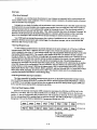
Fig. 1-15-
BaseAddressSwitch,51
52 - Buffer BypassSwitch (Factory Setting: OPEN (Not Bypassed))
Whenoperatingthe8255in Mode 1, thelinesof PortC functionascontrollines,someasoutputsandsomeas
inputs.WhenusingMode l, thePort C buffersmustbe removedandbypassedto allow theport C linesto be
individuallysetasinputsor outputs.Figure1-16showsthePortC buffen, andthefollowing stepst€ll you how ro
configurethe boardfor Mode I operation.
To removebuffering from port C:
l . CloseDIP swirches1 through8 on 52.
2. RemoveU8 from theboard.
3 . RemoveU9 from theboard.
CAUTION: Remember,wheneveryou closetheswitches,be sure to remove&e buffers,U8 andU9, from the
board.Failure to do so may damagetlre board.
1-r0
l
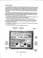
I/O CONNECTOR
P2 t P12
I
I
PIN16
PC7
PC6
PC5
PC/+
PIN 1.1
PIN 12
PC3
PC2
PC1
PC0
Fig.1-16- portC BufferCircuitry
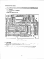
Pull-up/Pull-downResistorson Digitat VO Lines
The 8255programmableperipheralinrerfaceprovidesZ4TIIICMOS compatibledigial I/() lines which canbe
interfacedwitlr extemaldevices.Theselines aredivided into four groups: eightPort A lines, eight port B lines, four
Port C Lower lines, andfour Port C Upper lines. You caninstall and connectpull-up or pull-down resistorsfor any
or all of thesefour groupsof lines. You may want to pull lines up fonconnectiono switches.This will pull the 11nL
high whenthe switch is disconnectedor, you may want o pull lines down for connectionto relayswhich conrol
turning motorson and off. Thesemotorstum on whenthe digital linas controlling themare high. The port A urd
Port B lines of the 8255auomatically power up asinputs - which can float high - during the few momentsbefore
the boad is first initialized. This cancausetlre externaldevicesconnectedto theselinesto operateerratically.By
pulling theselines down, when ttredataacquisitionsyslemis first tumedon, the motorswill not switch on beforethe
8255is initialized.
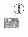
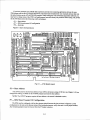
To usethe pull-up/pull-downfeanre, you must first insall 10kilohm resistorpacksin any or all of the four
locationsaroundthe 20-pin P12connectorand nearthe botom of thep2 Ilo connector,labeledpA, pB, pcl-, and
PCH.PA andPB take10-pinpacks,andPCL andPCH take6pin packs.Figure1-17showsa blowupof rhepA,
PCL, andPCHresisor packlocations.pB is locatedto theleft of pl2.
After theresistorpacksareinstalled,you mustconnecttheminto thecircuit aspull-upsor pull-downs.Locate
the three-holepadson the boardnearthe resistorpacks.They are labeledG (for ground)on one endand V (for +5V)
on tle otherend.The middleholeis common.PA is for PortA, PB is for Port B, PCL is for port C Lower,andpCIi
is for Port C Upper.Figure1-17showsthesepads.To operateaspull-ups,soldera jumperwire betweenthe
commonpin (middlepin of thethree)andthe V pin. For pull-downs,soldera jumperwire betweenthecommonpin
(middlepin) andtheG pin. Figurel-18 showsPort A lineswittr pull-ups,Port C Lower with pull-downs,andport C
Upperwith no resistors.
l-11
oooo
oooooo
oEr oo
OOe
66
oooooo
oooo
-.
-a--------;
oooooo
oooooooo
oo
oo
oot
oo
OO 62635 OO
oo
oo
oooooooo
oooooo
bThDehE&-qBhtga
Fig.1-17- Pull-up/Putt-down
Resistor
Circuitry
t-t2
8255
(
istJrJ
(
PoRr
c f
L O W E R(
(PA0-3)
[
YL .C€ OHO - r
u
o*
P O F TC
UPPER
(PA4-7)
Fig.1-18- AddingPult-ups
andpuil-downs
to Digitat
t/OLines
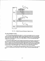
Gm, Gain Muttiplier Circuitry
1\e2700 hassoftwareprogrammable
binarygainsof l,Z,4,and 8. A gain multipliercircuit,Gm, is provided
so that you can easilyconfigurespecialgain settingsfor a specificapplication.Note that whenyou usethis feature
and setup the boardfor a gain of othertlan l, all of the input channeiswill operateonly at your customgain
sening.
In otherwords,if you installcircuiry which givesyou a gainmultiplierof 10,thentheiourprogrammablegains
availableare10,?n,40,and80.
Gm is derived by addingresistorsRl andR2, rimpot TR4, andcapacitorC46, alllocatedin the upperpart,just
to theright of centeron theboard.Theresistorsandtimpot combineto setthegain,asshownin the formulain
Figure 1-19'CapacitorC46 is providedso thatyou canaddlow-passfiltering in ne gain circuit.If your input
signal
is a slowly changingoneandyou do not needto measueit at a higherrate,you may wantto adda capacitor
ata46
in orderto reducetheinput frequencyrangeandin turn reducethe noiseon yotu input signal.The formulafor
settingthefrequencyis givenin thediagram.Figurel-19 showshow theGm circulry is configured.
As shownin Figurel-19, a soldershortmustbe removedfrom theboardo activatethe Gm circuitry.This short
is locatedon the bottom sideof theboardunderU27 (AD7L}IC). Figurel-20 showsthe locationof thesolder
short.
l-13
Removesoldershort
(seeFigure1-20)
To calculateGm:
Gm =[(TH4+ R2)/R1]+ 1
To calculatelrequency:
t=1t12nC46(R2+TRa)l
Fig.1-19- GainCircuitryand Formulas
tor Catcutating
Gm andf
FernoyeSolder Shorl
BetweenThese2 Padson
Bottom Slde of Board
oooo
oooooo
oq. oo
OOs OO
oooooo
oooo
ooo000
oooooooo
oo
oo
oo.
oo
00.e
oo
oo
oo
oooooooo
oooooo
Fig.1-20- Diagram
lor RemovalofSolderShort
t-14
CHAPTER2
BOARDINSTALLATION
The 2700boardis easyto installin your pCl/ef or compatible
computer.This chaptertells you step-by-step
how to install and
connectthe board.
After you haveinstalledthe boardandmadeall of your connections,you canturn your systemon andrun the 2700DIAC
boarddiagnosticsprogramincludedon your examplesoftwaredisk
to verify thatyour boardis working.
2-r
Board Installation
Keeptheboardin its antistaticbaguntil you arereadyto installit in yourcomputer.Whenremovingit from ttre
bag,hold the boardat theedgesanddo not [ouchthecomponents
or connectors.
Beforeinstallingtheboardin your computer,checkthejumperandswitchsettings.Chapter1 reviewshe
factorysettingsandhow to changethem.If you needto changeanysettings,referto theappropriateinstructionsin
Chapter1. Note that incompatiblejumper settingscanresultin unpredictableboardopetationand erraticresponse.
To install the board:
1. Turn OFF the powerto your AT computer.
2. Removethe top coverof thecomputerhousing(refero yourowner'smanualif you do not aheadyknow
how ro do this).
3. Selectany unusedexpansionslotandremovethe slotbracket.
4. Touchthemetalhousingof thecomputerto dischargeanysutticbuildupandthenremovettreboardfrom its
anrisaticbag.
5. If you areusingthe20-pinP12connectorfor 8255digitalI/O operations,
connectthematingconnectorto it
beforeinstallingtheboardin thePC.Notethat theY2IlO connectormountingbrackethasan oversized
cutoutto allow spacefor runningthe cableto Pl2 throughthesameVO slot.If you wantto run bothcables
throughthesameslot,you mustmaketheseconnections
beforeinstallingtheboard.
6. Holdingtheboardby its edges,orientit so thatis cardedge(bus)connectors
line up with ttreexpansionslot
connectorsin the bouomof theselectedexpansionsloL
7. After carefullypositioningtheboardin theexpansionslot so thatthecardedgeconnectors
arerestingon the
computer'sbusconnectors,
gentlyandevenlypressdownon theboarduntil it is securedin theslot.
NOTE: Do not forcetheboardino the slot.If theboarddoesnot slideinto place,removeit andry again.
Wiggling the boardor exert"ingtoo muchpressurecan resultin damageto the boad or to the compub;.
8. After the boardis installed,securethe slot bracketbackino placeandput the coverback on yotu compurcr.
Theboardis now readyo be connected
via theext€malI/O connectorat therearpanelof yourcomputer.Be
sureto observethekeyingwhenconnectingyour externalcableto the I/O connector.
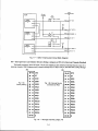
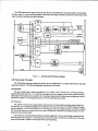
External VO Connections
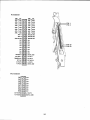
Figure
2-l shows
the2700's
P250-pinVOconnector
andpl2 on-board
20-pinconnector
pinous.Refertothese
diagramsasyou makeyour I/O connections.
2-3
A|ltr
att€
A|t{3
A||{a
att{5
Allltr
Alttb
AllB+
Allll+
Alll5+
Al116+ All€
alM. I Alt.e
A|lA- | X]tto
aD& | atMr
AN+ | Arttz
alila I Attfr3
A|lF I ltiha
AIlfl+
A|lft
arit- | a|ltrt
Alt{8.
altr5
A|l{& I Alinc
AOIJT I
AIIALG
GIIO
AOIJT 2
A}IAL6
OND
al{aloc
tH@En
ol{o
atrAL(E ol{o
PA7
Pgt
PK
FOt
PAI
FCr
PAI
PCa
P3
FGI
PA2
FCt
PAI
FC'l
P0
FCO
til
ETT GAIE T
THCCEn OUr
ETT CLK
P80
PC0
PE.I
PCr
?E2
PC2
PAt
PC3
PB.
PCa
TrcotTr
T/CO{rT2
Ptt
PCr
PEI
PCt
gT CATE 2
Pgl
DICITALGIIO
+12 YOLIS
$ VOLn]
-r2 Yotts
DIOITALOIID
PgI
+t2 VOLTS
+6 YOLTS
.r2volts
OIGITALGI'O
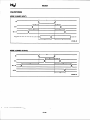
pinAssignments
Fig.2-1- P2 l/OConnector
andPl2 On-board
Connector
Connectingthe Analog Input Pins
The analoginputson the 2700 canbe set for single-endedor differential operation.
NOTE: It is goodpracticeto connectall unusedchannelsto ground,as shownin the following diagrams.
Failure to do so may affect the accuracyof your results.
Single'Ended. When operat"ingin the single-endedmode,connectttre high side of the analoginput to oneof
the analoginput channels,AINI throughAIN16, and connectthe low side to an ANALOG CXp-tpins Ig and,2U2T
on P2). Figure 2-2 showshow ftese connectionsare made.
Differential. Whenoperatingin the differential mode,twistedpair cableis recommendedo reducethe effects
of magneticcoupling at the inputs.Your signalsourpemay or may not havea separategroundreference.When
using the differential mode,you shouldinstall a l0 kilohm resistorpackat locarionRN7 on the boardo provide a
referenceto ground for signalsourceswithout a separategroundreference.
Firsl connectthe high sideof the analoginput to the selectedanaloginput channel,AINI+ throughAINS+, and
connectthe low side of the input to the conespondingAIN- pin. Then,for signal sourceswith a separateground
reference,connectthe groundfrom the signal sourceto an ANALOG GND (pins 18 and 20-22 ony2). Figure 2-3
showshow theseconnections
aremade.
24
2700
t/o cot{l{EcToR
P2
I
I
SIGI{AL
touRcE
1 our
P|lt t
t
AtN t
GND
a
a
a
a
a
a
O
a
a
IUX
O U T+
SIGNAL
SOURCE
15 our
At|t t5
oul .
GND
Ptt|
AIN I6
I
I
I
I
I
I P||t 22
Fig.2-2- Single-Ended
InputConnections
2700
I/O CONNECTOR
P2
I
I
I
lt'*,
SIGNAL
sOURCE
I out
i
IPIN2
a
o
a
AIN lr
RN7
I
.l
.l
.l
rruE
I
AIN t.
a
.
OUT +
| ,," ,.
'
ttl
ltl
lPtN,r4
z our{
(-
IUX
I
a
a
a
I
I
I
SIGNAL
T
I
I
I
AIN 7+
OUT .
|
|
AtN 7.
I
I
GND
rl
ll
ll
lPtNis
.-t
I
AIN 8r
,!-$uri Ll
ii
ll
\-
AtN 8-
] ert aa
Fig.2-3- Differential
InputConneclions
2-5
+
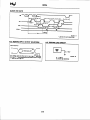
Connectingthe Trigger In and Trigger Out pins, CascadingBoards
The 2700 boardhasan externalrigger input (P2-39)andoutput(Y243) so rhatconversionscanbe starred
basedon externalevents,or so that two or moreboardscan be cascadedandrun synchronouslyin a "master/slave"
configuration.By cascadingtwo (or more)boardsas shownin Figure 24,they can be triggeredto startan A/D
convenion at the sametime (samplinguncertaintyis lessthan50 nanoseconds).
When you cascadeboards,be sure
to set eachboardfor a different baseaddress(seeChapterl), or systemcontentionwill result
NOTE: When cascadingboards,the samplinguncertaintyis lessthan 50 nanoseconds.
If this level of uncertainty is too geat for your application,you canconnectthe rigger signalto the trigger input of eachboard.In this
configuration,the boardsarenot cascaded,but ratherdrivenby the samerigger pulseat the sametime, and the
samplinguncertaintyis reducedo lessthan 5 nanoseconds.
If you apply an externalrigger to the hard's rigger in pin, note that a jumper shouldbe installedon ET on p7
(seeChapterl). The boardis triggeredon the positive edgeof thepulseand the pulsedurationshouldbe least
at
100
nanoseconds.
2700
t/o coNNECToR
P2
I
I
I
B O A R OT 1
(MASTER)
BOARO ,2
(SLAVE)
ilux
SIGNAL ,
souRcE| '
z ourJ
(-
PIN 1
AlNl +
I
!prrz
I
I
AIN1 .
r0K
I
I p'* .t
TRIGGER IN
Fig.2-4 - CascadingTwo Boardsfor SimultaneousSampling
Connectingthe Analog Outputs (ADA2700Onty)
For eachof the two D/A outputs,connectthe high sideof thedevicereceiving theouput O tfie AOUT channel
F2-17 or P2-19)andconnectthe low sideof thedeviceo anANALOG GND (P2-18orY2-20\.
Connectingthe Timer/Countersand Digital VO
For all of theseconnections,
thehigh sideof an externalsignalsourceor destinationdeviceis connectedto the
appropriatesignalpin on theP2 VO connectoror on P12,andthelow sideis connected
to any DIGITAL GND.
Runningthe2700DtrAG
Diagnostics
Program
Nowthatyourboardis readyto use,youwill wantto ry it out.An easy-to-use,
menu-driven
diagnostics
program,
2700DIAG,
is included
you can
withyourexample
software
to helpyouverifyyourboard'soperation.
alsousethisprogramto makesurethatyourcurrentbaseaddress
settingdoesnotcontendwith anotherdevice.
2-6
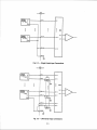
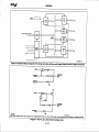
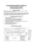
CHAPTER3
HARDWARE DESCRIPTION
This chapterdescribesthefeaturesof the 2200hardware.The
majorcircuitsarethe A/D, the D/A, the timer/counters,
andthe
digital vo lines.This chapteralsodescribesthehardware-selectableinterrupts.
3-l
3-2
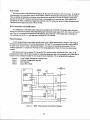
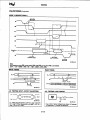
The2700boardhasfourmajoncircuirs,theA/D,rheD/A (ADA27CCI
only),chetimer/counters,
andthedigifal
VOlines.Figure3-1showstheblockdiagnmof ttreboard.Thischapterdescribes
thehardware
whichmakesupthe
majorcircuis andhardware-selectable
intemrps.
Fig.3-1- AD2700/ADAZ700
BlockDiagram
A/D ConversionCircuitry
The2700 performsanalog-o-digital conversionson up o 8 differential or 16 single-endedsofrware-selectable
analoginput channels.The following paragraphsdescribethe AID circuirry.
Analqg Inputs
The input voltagerangeis jumper-selectable
for -5 to +5 volts,-10 o +10 volts,or 0 to +10 volts.Softwareprogrammable
binarygainsof l,2,4,and 8 let you amplifulowerlevel signalsto morecloselymatchtheboard's
input ranges.Thesegainscanbe customizedfor evengreaterinput controi by addinga gain muttiplying circuit
as
describedin Chapterl. overvoltageprotectiono +35 volts is providedat theinpus.
A"/DConverter
The AD678 12-bitsuccessive
approximationA/D converteraccuratelydigitizesdynamicinput voltagesin 5
microseconds,for a maximumthroughputrateof 200 kIIz for the converteralone.Thi AD678 cbnains a sampteand-holdamplifier, a L2-bitAlD converter,a 5-volt reference,a clock, and a digiat interfaceto provide a ,orpl"t"
A/D conversionfunctionon a singlechip.Its low-powerCMOS logic combinedwith a high-precision,
low-noise
designgive you accurateresults.
Conversionsarecontrolledthroughsoftware(internally rriggered)or by an externalrigger broughtonto ttre
boardthroughthe I/O connector.An on-boardpacerclock canbe usedto control the conveisionrate.Conversion
modesaredescribedin Chapter4, Board Operationandprogramming.
3-3
Data Transfer
The converteddatacanbe ransfened throughthe PC databus to PC memoryin oneof two ways: by usingthe
microprocessoror by using direct memoryaccess(DMA). Databus transferstakemore processortime to execute.
They useponing and intemrptsto determinewhen datahasbeenacquiredand is readyfor ransfer. DMA places
datadirectlyinto thePC's memory,onebyteat a time,with minimaluseof processoitime.DMA nansfersare
managedby theDMA controllerasa backgroundfunctionof thePC, lettingyou operateat higherthroughputrates.
The maximumthroughpurrareof the2700is 150kHz.
D/A Converters(ADA2700Onty)
Two independent12$it analogoutputchannelsare includedon the ADA2700. The analogoutputsare generatedby two 12-bitD/A converterswith independent
jumper-selecable
outputrangesof 15, +lb, 0 to +5, orb m +10
volts.The+10 volt rangehasa resolutionof 4.88 millivolts,the+5 and0 to +10 volt rangeshavea resolutionof
2.44millivolts, andthe0 to +5 volt rangehasa resolutionof l.22millivolts.
Timer/Counters
An 8254programmableinterval timer providesthree l6-bit, g-MHz timer/countersto supporta wide rangeof
timing andcountingfunctions.Two of thetimer/counters,
TCOandTCl, arecascaded
so that theycanbe usedfor
the pacerclock. The pacerclock is describedin Chapter4. You can usethe remainingtimer/counter,TCZ, for
countingapplications,or cascadeit to TCOandTCI for timingapplications.
Figure3-2 showsthe timer/counter
circuiry.
Eachtimer/counterhastwo inputs,CLK in andGATE in, and oneoutput, timer/counterOUT. They canbe
programmedasbinary or BCD down countersby writing the appropriatedatato the commandword, asdescribedin
Chapter4. The commandword also lets you setup the modeof operation.The six programmablemodesare:
Mode 0
Mode I
Mode 2
Mode 3
Event Counter(ntemrpt on Terminal Count)
Hardware-Retriggerable
One-Shot
RateGenerator
SquareWave Mode
!-;;------'i
lltEB/
COUNT€R
0
2700
I/O CONNECTOR
P2
TO A/O
TRIGGER
I
I
I
EXT CLK
CLK
GATE
OUT
ptn lr I Ext cltE r
I
prruge
lrRrccen rn
I
p t r o z .T/C
l OUT 1
GATE 2
T/C OUT 2
L---------.;
:
Fig.3-2 -8254 Timer/Counter
CircuitBtockDiagram
34
Mode 4
Mode 5
Sofnvare-TriggeredSrobe
HardwareTriggeredSnobe(Reriggerable)
Thesemodesaredetailedin the 8254Data Sheet"reprintedfrom Inrel in Appendix C.
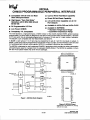
Digital VO, ProgrammablePeripheralInterface
The programmableperipheralinterface@pI) is usedfor digital I/O functions.This high_performance
TTL/
CMOScompatiblechip has24 drgitalI/O linesdividedinro two groupsof 12lineseach:
Group A - Port A (8 lines) andPort C Up'per(4 lines);
GroupB - Port B (8 lines) andPort C Lower (4 lines).
Port A andPort C areavailableat ttreextemalVO connector,p2. fort B andport C are availableat the on_board
20-pinconnector,P12.You canusethesepors in oneof two PPIoperatingmodes,Mode0 or Mode l. Do not try
to useMode 2 operation! The 2700doesnot supportMode 2. Whenoperatingin Mode l, the on-boardbuffen
mustbe removedfrom thePort C lines. This procedureis describedin ChapterI in ttre52 DIP switch discussion.
The 2700 operatingmodesare:
Mode 0 - Basic input/ouput. Lets you usesimpleinput andoutputoperationfor a port Datais written to or
readfrom the specifiedport.
Mode I - Strobedinput/output.Lets you ransfer VO daa from Port A or Port B in conjunctionwith strobesor
handshaking
signals.
Thesemodesaredetailedin the8255DataSheet"reprintedfrom Intel in AppendixC.
Thebidirectionalbufferson the8255'sVO linesmonitorthe8255controlword ro auomaticallysetrheir
direction.Hardwarechangesto the buffer circuitry arerequiredonly when usingMode l, wheretheport C buffers
mustbe removedasdescribedin Chapterl.
Interrupts
The27N hasfour jumper-selectable
intemrptsources:end-of-convert,
DMA done,the externaltrigger,and the
outputof timer/counter2. The end-of+onvertsignalcanbe usedtrcinterruptthe computerwhen an A,/Dconversion
is completed.The DMA doneis usedin the DMA modeto signalan intemrpt whenevera DMA transferis completed.The externaltrigger at the VO connectorcanbe usedto generatean intemlpt whenevertre trigger line
changesfrom low to high.Or, theoutputof timer/counter
2 cangenerate
an intemrptwheneverthecountreaches0.
ChapterI tellsyou how to setthejumpenson theintemrptheaderconnectorF8, andChapter4 describeshow to
programintemrpts.
3-5
3-6
CHAPTER4
BOARDOPERATIONAND PROGRAMMING
This chaptershowsyou how to prognrmanduseyour 2700
boardby writing to andreadingfrom the AT busin 8- or 16-bit
words.It providesa completedescriptionof theVO map,a detaileddescriptionof programmingoperationsandoperatingmodes,
andflow diagramsto aid you in programming.The example
pfogfilrnsincludedon thedisk in your boardpackagearelistedat
the endof this chapterTheseprograms,writtenin Turboc and
TurboPascal,includesourcecodeto simplify your applications
programming.
Definingthe VO Map
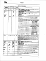
Th. VO mapfor the AD2700andADA2700is shownin Table4-l betow.As shown,the2T}}occupies32
consecutiveVO port locations.
Becauseof the lGbit struc[re of the AT bus,everyotheraddresslocation is used.Our programmingstructure
usesthe l6-bit commandfor readingttreAID converteddataandfor programmingthe nvo ADA2700 D/A converters.All otherread/writeoperationsare 8-bit operations.
, The baseaddress(designatedasBA) canbe selectedusingDIP switch Sl asdescribedin Chapterl,Board
Setrtngs.This switch can be accessedwithout removingthe boardfrom the connecbr. Sl is facory
setat 300 hex
(768 decimal).The following sectionsdescribethe regisrercontentsof eachaddress
usedin the VO map.
Tabfe4-1-AD27O0/ADAATWUOMap
ReglsterD,escrlptlon
ReadFunalon
Wrhe Functlon
Address'
(Declmal)
Read Data/Stad Conv€rt
Read 12-bit ArlDconverted
data word
StartA/Dconversion
BA+0
ReadStatus/Reset
Readstatusword
Resets board so thai it is
ready to start A/D oonversions
B A +2
Ghannel/Gain/
Board
Funclions
Programchannel& gain;
Readcurrentchannel& gain exlsrnallriggerenable,IRQ
ssttings
enable
BA+4
Reserved
Not used
B A +6
D/A Converter1
(ADA2700
Only)
D/AConverter2
(ADA2700
Only)
Notused
Not used
Program12-bitDAC1and
startconversion
Program12-bitDAC2and
stadconversion
B A +1 0
Reserved
Not used
Not used
BA+12
Reserved
Not used
8255PPIPortA
Not used
Notused
ProgramPortA digitaloutput
ReadPortA digilalinputlines lines
BA+8
BA+14
B A +1 6
8255PPIPortC
ProgramPodB digitaloutput
ReadPortB digitalinputtines lines
ProgramPortC digitaloutput
ReadPortC digitalinputlines linEs
BA+20
8255PPlControlWord
Notused
ProgramPPIconfiguration
BA+22
Readcount value
Loadcountregister
BA+24
8255PPIPortB
8254Timer/Counter
0
(Usedfor pacerclock)
8254Timer/Counter
1
(Usedfor pacerclock)
B A +1 8
Readcount value
Loadcountregister
BA+26
S254TimerlOounlet 2
(Availablefor externaluse) Readcount value
Loadcountregister
BA+28
8254Timer/Counter
ControlWord
Programcountermode
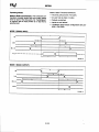
BA+30
Notused
* BA = B35s Address
4-3
BA + 0: ReadData/Start Convert (ReadAilrite)
16'bit operation. A readprovidesthe 12-bitA/D converreddatain a rightjustified formatasshownbelow.
Whenjumperson P4 andP15aresetfor bipolarconversions,
thedataword's four mostsignificantbis matchthe
MSB of theA/D converteddataOit 12).This is necessary
to providetheconecttwoscomplementrepresentation
of
theconverteddata.WhenP4 andP15aresetfor unipolarconversions,
tlresetop four bits are0.
A write star8 an A,lD conversion(datawritten is irrelevant).
BIPOLARDATAWORD:
D l 5 D l 4 D l 3 D12 D l 1 D l 0
D9
D8
D7
D6
D5
D4
D3
D2
D1
DO
B i t 1 2 B i t 1 2B i t 1 2B i t 1 2B i t 1 2B i t 1 1B i t l o B i t g B i t S Bit 7 Blt 6 Bit s Bit 4 Bit 3 Bttz Bit 1
(MsB)
(LSB)
UNIPOLAR
DATAWORD:
D 1 5 D 1 4 D 1 3 D12 D l 1 D l 0
0
D9
D8
D7
D6
D5
D4
D3
D2 D1
DO
Bit12Bit11
Bit10Bir9Bit8 BitT Bit6 Bits B1t4 BitS Bit2 Birl
(MSB)
(LSB)
BA + 2: Read StatuVReset(ReadAilrite)
t'bit operation. A readprovidesthe four sanrsbits definedbelow.The end-of+onvertbit goeshigh whena
conversionis completeanddoesnot go low until the datais read,useful informationwhenusing e*te-il triggering
to startconversions.The DMA donebit goeshigh whenyou are in the DMA modeand the DMA uansferis
complete.The IRQ statusbit goeshigh whenan intemrpt hasoccurredand stayshigh until a resetcommandis sent
(BA + 2). D3 showsthes[atusof eithertheA/D converterstatussignalor theexternalgateinput for timer/counter2,
dependingon the settingofjumper Pl4. Unlike theEOC statusat bit 0, theA,/Dconverterstahs goeslow whena
conversionstartsand thengoeshigh as soonas the conversionis completed.When the input tr,asUeensampledand a
conversionis in progress,this line goeslow. At this time,theanaloginputchannelcanbe changed,allowing
maximumthroughputfor channelscanning.
A write resetsinternalregisten so that the boardis readyto startconversions.The datawritren is inelevant; the
act of writing to this addressclearsthe board.A resetcommandresetsthe end-of-convert,DMA done,and IRe
statusbits to 0.
D7
D6
D5
D4
D3
D2
A/D CONVERTER
Status
0=converling
1=notconverting
EXTGATE2 Status
monitorsexternalgate
2 line
|
|
|
I
I
|
|
D1
End-of-Convert
End-o
|
0 ==nnooE O C
O
|
|
l1==cconversion
o
done
I
DMADone
te
0 = DMAnot
1ot done
dor
1 = DMAdone
IRQStatus
0=NolRQ
1=tRQ
44
DO
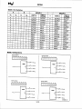
BA + 4: ChanneVGain/BoardFunctionsSelect(ReadAVrite)
t-bit operation. Programsthe analoginput channelandgain, and enablesthe IRQ and extemalrigger.
Readingthis registershowsyou the currentsettings.
AnalogInput
ChannelSelect
0000= channel1
0001= channel
2
0010= channel
3
0 0 1 1= c h a n n e l 4
0100 = channel
5
0101= channel
6
0110=channelT
0 1 1 1= c h a n n e l 8
1000= channel9
1001= channel
10
1010- channel
11
1 0 1 1= c h a n n e1l2
1 1 0 0 = c h a n n1e3l
1101= channel
14
1 1 1 0= c h a n n e1l5
1111=channel16
lRQ Enable
0 = IRQdisabled
1 = IRQenabled
ExternalTrlggerEnable
0 = Disabled
1 - Enabled
ChannelGaln
00=x1
0 1- x l
10*x4
11=x8
BA + 6: Reserved
BA + 8: D/A Converter1(ADA2700DACI) (Write Onty)
16'bit operation. Programsthe 12-bitdigital word for DACI in a right-justifiedformatasshownbelow.The
act of writing o this port startsa D/A conversionon channell.
D l 5 D l 4 D l 3 D12 D l 1 D l 0 D9
X
x
D8
D7
D6
D5 D4
D3
D2
D1
DO
B i t 1 28 1 t 1 1B i t l 0 B i r g B i t S B i r T B i t 6 B i r s B i r 4 B i t 3 B 1 t 2 Bit 1
(MSB)
(LSB)
BA + 10: DIA Converter 2 (ADA2700DAC2) (IVrite Onty)
l6'bit operation. Programsthe 12-bitdigital word for DAC2 in a right-justifiedformatasshownbelow.The
act of writing o this port startsa D/A conversionon channel2.
D l 5 D t 4 D l 3 D12 D l 1 D l 0
X
x
D9
D8
D7
Bit 12 Bit 11 Bit10 Bit9 Bit8
(MSB)
BA + 12: Reserved
BA + 14: Reserved
4-5
D6
D5
D4
D3 D2
D1
DO
8rt7 Bit 6 Bit s Bit 4 Bit 3 Bit 2 Bit 1
(LSB)
BA + 16: PPI Port A - Digital UO (Read/Write)
8'bit operation. Transfersthe 8-bit Port A digital inputanddigial outputdatabetweenttreboardandan
externaldevice.A readEansfersdatafrom the exernal device,throughP2, and into PPI Port A; a write ransfers the
written daa from Port A throughP2 to an extemaldevice.
BA + 18: PPI Port B - Digitat I/O (ReadAilrite)
8'bit operation. Transfersthe8-bit Port B digital inputanddigitrl outputdatabenveenthe'boardandan
externaldevice.A readtransfersdatafrom the exemal device,throughP12 (the on-board20-pin connector),and
into PPI Port B; a write transfersthe written datafrom Port B throughPl2 to an externaldevice.
BA + 20: PPI Port C - Digitat I/O (ReadAilrite)
E'bit operation. Transfersthe two 4-bit Port C digial input and digiml ourputdatagroups(port C Upper and
Port C Lower) betweenthe boardandan externaldevice.A readtransfersdatafrom the Jxternaldevice,tlrbugh p2
andPl? (the on-board20'pinconnector),and into PPI Port C; a urite transfen the wriuen datafrom port C 41fougn
Y2 andP12to an externaldevice.
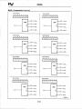
BA + 22: 8255PPI Control lVord (tVrite Onty)
8'bit operation. Whenbit 7 of thisword is setto l, a write progamsthePpI configuration.Bit 6 mustalways
be set to 0 (Mode 2 operationis not supportedby tre 2700).
D7
Mode Set r's
1 = aclive
D6
D5
D4
D3
D2
D1
DO
---l
i
!*
lde Sels(:t
* mode
= modg
t t - modg j
i3i
I
I
I
I
I
PortA
0 = output
1 = input
PortC Upper
0 = output
1 = input
GroupA
4-6
|
|
|
ll
I
|
|
|
|
|
Portc
t C Lower
o = output
our
1 = input
inp
PortB
0 - ourpur
1 = input
I
ModeSelect
0=mode0
1=mode1
L_
--JY!-BJ
The tablebelow showsthe connol words for ttre 16possibleMode 0 port
vo combinations.
8255Portl/OFlowDlrectionandControtWords,
Mode0
GroupA
GroupB
ControlWord
PortA
Port C
Upper
Porl B
PortC
Lower
Outpul
Output
Output
Output
Output
Output
Output
Output
Output
Output
Blnary
Declmal
Hex
10000000
128
80
Input
10000001
129
81
Input
Output
130
82
Outpul
Input
lnput
10000010
10 0 0 0 0 ' t ' l
131
83
Output
Input
Output
Output
10001000
136
88
Output
Input
Output
Input
10001001
137
89
Output
Input
Input
Output
10001010
138
8A
Output
lnput
Input
Input
10001011
139
8B
Input
Output
Output
Output
10010000
144
90
Input
Output
Output
Input
10010001
145
91
Input
Output
Input
Output
10010010
146
92
lnput
Output
Input
Input
10010011
147
93
lnput
Input
Output
Output
10011000
152
98
Input
Input
Output
lnpul
10011001
153
99
Input
Input
lnput
Output
10011010
154
9A
Input
Input
lnput
lnput
10011011
155
9B
Whenbit 7 of the PPI conrol word is setto 0, a write canbe usedto individually progmm port
the
C lines.
D7
D6
D5
D4
SeVReset
FunctionBit
0 = active
D3
D2
Blt Select
000= Pco
001= Pc1
010= Pc2
0 1 1= P C 3
100= PC4
101= PCs
1 1 0= P C 6
1 1 1= P C 7
4-7
D1
DO
Blt SeUReset
Blr
0 == s e t b i t t o 0
1=S€tbittol
For example,if you want to setPort C bit 0 to 1, you would setup thecontrolword so thatbit 7 is 0; bits 1, 2,
and 3 are0 (this selectsPC0); andbit 0 is 1 (this setsPCOto 1). The control word is setup like this:
D7
D6
D5
D4
D3
D2
D1
X = don'tcare
SeVReset
FunctionBlt
DO
SetsPCOto 1
(written
loBA+22)
Set PCO
Blt Sefect
000= PCO
BA + 24: 8254Timer/Counter 0 (Read/Write)
8'bit operation. A readshowsthe countin the counter,and two write operationsload the counterwith a new
16'bit valuein two 8-bit steps,LSB followedby MSB. Thecountermustbe loadedin two 8-bit sreps!Counting
beginsas soonas the count is loaded.This counteris cascadedwith TCI o form the 32-bit on-boardpacerclock.
BA + 26: 8254Timer/Counter 1(Read/Write)
8'bit operation. A readshowsthe count in the counter,and two write operationsload the counterwith a new
16-bitvaluein two 8-bit steps,LSB followedby MSB. Thecountermustbe loadedin two 8-bit steps!Counting
beginsas soonas the count is loaded.This counteris cascadedwith TCOto form the 32-bit on-boardpacerclock.
BA + 2E: E254Timer/Counter 2 (Read/Write)
8'bit operation. A readshowsthe count in the counter,and two write operationsload the counterwith a new
16-bitvaluein two 8-bit steps,LSB followedby MSB. Thecountermusrbe loadedin two 8-bit sreps!Counting
beginsas soonas tle count is loaded.This countercanbe cascadedto TCOand TCI or it can be usedindependently.
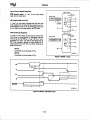
BA + 30: 8254Control Word (Write Only)
8-bit operation. Accesses
the8254controlregistero directlyconkol thethreetimer/counters.
D7
D6
D5
D4
D3
D2
D1
DO
BCD/Blnary
0 = binaU
1=BCD
CounterSelect
Selec
00 = Counter
0
01 = Counter1
10= Counter
2
11= readbacksetting
Read/Load
00 = latchingoperation
01 = read/load
LSBonly
10 = read/load
MSBonly
11= read/load
LSB,thenMSB
4-8
Counterilode Select
Counter
000= Mode0, eventcount
001= Mode1, programmable
1-shot
010= Mode2, rategenerator
011= Mode3, squarewavsrategenerator
100= Mode4, software-triggered
strobe
101= Mode5, hardware-triggered
strobe
Programming the 27fi)
This sectiongivesyou somegeneralinformationaboutprogrammingand ttreAD2700 and ADA2700 boards,
and thenwalks you throughthe major 2700programmingfunctions.Thesedescriptionswill help you as you usethe
exampleprogruns includedwith the boardand the programmingflow diagramsat the end of this chapter.All of the
progzun descriptionsin this sectionusedecimalvaluesunlessotierwise specified.
The 2700 is programmedby writing to andreadingfrom the correctVO port locationson the board.These
VO
ports weredefinedin the previoussection.Becausethe 2700 is AT bus compatible,readingthe A/D converter
data
and writing the D/A converterdatais donein a l6bit word format. All other operations61idon" in an 8-bit word
formal High-level languagessuchasPascal,C, and Cr+ makeit very easyto readlwritetheseports.The table
below showsyou how to readfrom and write to Vo ports in Turbo C andTurbo pascal.
Language
TurboC
Bead8 Blts
tYrite8 Blts
Reed16Bits
Wrlh16Bits
Dala= inp164166r.ur;oulponb(Address,
Data) Data=inpo11466put1 outpod(Address,
Data)
TurboPascal
Data:=PorllAddress] Poil[Address]:=
Dda
Dala:=PortW[Address]PorlWlAddressl:=
Data
In addition to beingable o read/writethe VO pors on the 2700,you mustbe able o perform a variety
of
operationsthat you might not normally usein your programming.The tablebelow showsyou some
of the operaton
discussed
in this section,with an exampleof how eachis usedwith pascalandc.
Language
c
Modulus
IntegerDlvision
Vo
3=b7oC
Pascal
MOD
a:=bMODc
AND
OR
I
?=b/C
&
a=b&c
a=b;c
DIV
a:-bDlVc
AND
a:=bANDc
OR
a:=bORc
Many compilershavefunctionsthat canreadlwriteeither 8 or 16bits from/to an I/O porr For example,
Turbo
PascalusesPort for 8-bit port operationsandPortW for 16bic, Turbo C usesinportb for an
8-bit readof a port
andinport for a 16-bitread.Be sure to usethe correct function for E- and 16-bit operationswith
the 2700!
Clearing and Setting Bits in a port
When you clear or set one or morebits in a port, you mustbe carefulthat you do not changethe satus
of the
otherbits. You canpreservethe saars of all bits you do not wish to changeby properuseof th! AND
andOR
binary operators.Using AND and OR, singleor multiple bis canbe easilycteareoin one operation.
To clear a singlebit in a port, AND the curent valueof the port with the valueb, whereb = 2552u,.
Exanple: Clearbit 5 in a port.Readin thecurrentvalueof theport, AND it wittr 223
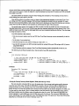
(223 = 255 - 2s),and thenwrite the resultingvalue to theport. In pascal,this is programmed
as:
p
o
r
t
V :=
lportAddressJ,.
V := V AND223;
Port [PortAddress] := V;
To seta singlebit in a port, OR thecurrentvalueof theport with thevalueb, whereb = /tir.
Example: Setbit 3 in a port.Readin thecurrentvalueof theport, OR it with 8 (8 = 23),andthen
write theresultingvalueto theport. In pascal,this is programmed
as:
V := port lportAddress],.
V := V OR B;
Port [PortAddress] := V;
4-9
Seningor clearingmore thanonebit at a time is accomplishedjust aseasily.To clear multiple bits in a port,
AND the currentvalue of the port with the valueb, whereb = 255 - (the sum of the valuesof the bits to be cleared).
Note that the bis do not haveto be consecutive.
Example:Clearbis2,4,and6inaporlReadinthecunentvalueof
theport,ANDitwith 171
(171= 255 - 22- Y - 2'\, andthenwrite theresultingvalueto ttreport"In C, this is programmed
:ts:
v : inportb (port_address) ,.
v=v&171,.
outportb(port_address,
v) ;
To set multiple bis in a port, OR the currentvalue of the port with the valueb, whereb = the sumof the
individual bits m be set.Note that the bis to be setdo not have!o be consecutive.
Example: Setbis 3, 5, and7 in a port.Readin thecurrentvalueof theport, OR it with 168
(168= 23+ 2s+ 2), andthenwrite theresultingvaluebackto theport In C, this is programmed
zts:
v : inportb(port_address),.
v=v
I 158;
outportb (port_address, v) ;
Often, assigninga rangeof bits is a mixture of settingand clearingoperations.you can setor cleareachbit
individually or usea fastermethodof first clearingall drebis in the rangethen seningonly thosebis that mustbe
set usingthe methodshownabovefor settingmultiple bits in a port. The following e*a*pie showshow this twostepoperationis done.
Example: Assignbits 3, 4, and 5 in a port to 101(bits 3 and 5 set,bit 4 cleared).First, read in rhe
port and clearbis 3, 4, and 5 by Al.{Ding themwith l99. Then setbirs 3 and 5 by ORing them
with 40, and finally write the resultingvalueback to the pon In C, this is programmedas:
v = inportb(port_address)
;
v:vC199;
v:v
| 40;
outportb (port_address, v) ,
A final note: Don't be intimidatedby the binary operatorsAND and OR andtry to useoperatorsfor which you
havea betterintuition. For instance,if you areBmpted to useadditionand subracdon to setand clear bis in place
of the methodsshownabove,DON'T! Addition and subraction may seemlogical, but they will not work if you
try
to clear a bit ttratis alreadyclear or seta bit that is alreadyset.FG example,you might think that to setbit 5 of
a
porq you simply nepdto readin tle port, add32 (25)to that value,and thenwrite the resultingvalue
back to the port.
This works fine if bit 5 is not alreadyset.But, what happenswhenbit 5 rs alreadyset?Bits O-to+ witt be unaffected
andwe can't sayfor surewhathappensto bits 6 andT,butwe cansayfor surethatbit 5 endsup clearedinsteadof
being ser A similar ploblem happenswhen you usesubtractionto cleara bit in placeof the methodshownabove.
Now that you know how to clear and setbits, we arereadyto look at the programmingstepsfor the 2700 board
functions.
A./DConversions
The following paragraphswalk you throughthe programmingstepsfor performingA/D conversions.Detailed
information aboutthe conversionmodesis presentedin this section.You canfollow ttrise stepson the flow diagmmsat theendof ttrischapterandin our exampleprognmsincludedwith theboard.In this discussion,BA
refers
to the baseaddress.
. Initializing the Board
Start your programby resetting the 27ffi board.This is doneby writing to the CLEAR porr locared atBA + z.
The actualvalue you write to this pon is irrelevant.After resettingthe boardfollowing po*ir-op, take an AID
4-10
readingand throw it away to makesurethe converteris initialized and conains no unwanteddata.After the A/D
readingis taken,senda secondCLEAR commandto BA + 2. After clearingthe board,you may want
to initialize
the 8255for Mode 0 or Mode I operationandconfigureyour VO. Refer o the g255conrol word descriprion,
BA+ 22, presented
earlierto determinethe valueof theword you write for initialization.Now ttreboardis initialized andreadyto run.
. Selectinga Channel
To selecta conversionchannel,you mustassignvaluesto bits 0 through3 at BA + 4. The tablebelow
shows
you how to determinethebit settings.Note thatif you do not wantto changethegain
setting,alsoprogrammed
throughBA + 4, you mustpreserveit whenyou setthechannel.
x
x
x
cH3
cH2
cH1
cH0
Channel
cH3
cH2
cH1
cH0
0
0
0
0
0
0
0
1
0
0
0
0
0
1
I
10
0
0
0
0
0
1
0
1
0
0
1
1
1
11
12
13
1
a
I
0
1
0
1
0
0
1
0
1
14
I
1
o
1
1
0
t
1
7
0
0
0
15
1
1
1
8
0
1
1
1
16
,|
0
1
1
Channel
I
2
4
5
o
cH3 cH2 cH1 cH0
x
1
1
BA+4
. Settingthe Gain
You maychooseamongthe variouslevelsof programmable
gainby settingbits4 and5 at BA + 4. The able
belowshowsyou how to determinettrebit settinggforthe gainy;u nod. If you have gain
a
multiplyingresistor
installedasdescribedin Chapter1, thenorrractualgain valueswill be thosein
the table-multipliedby the gain
multiplier'svalue.Note thatif you do not wantto changethechannelsetting,alsoprogrammed
throughBA + 4, you
mustpreserveit whenyou setthegain.
x
x
G1
GO
x
x
Galn
G1
GO
1
0
4
0
0
,|
8
1
2
x
x
BA+4
1
0
1
. Enablingand Disablingthe ExternalTrigger
Any time you usetheexternaltriggeror thepacerclock,this bit at port BA + 4 mustbe sethigh
to enableAID
conversions.
. Enablingand DisablinCIRQ
Any time you useintemlpts,this bit at port BA + 4 mustbe sethigh to enabletheon-boardinterrupt
circuitry.
. ConversionModes/Triggering
The2700hasttrreeriggering (conversion)modes.Figure4-l showst6etiming diagramfor Al) conversions.
This sectiondescribestheconversionmodes.
4-ll
Trigger
End-of-Convert
(EOC)
Read
Fig.4-1-A/D Conversion
Timing
Diagram,
AllModes
Internal vs. External Triggering. with internalriggering (alsocalled softwareriggering), conversionsare
initiated by writing a valueto the START COI.IVERTport at BA + 0 on the board.Wiilr lxternal triggering,
conversionsare initiated by applyinga high TTL signalwith a pulsedurationof at least 100nanoseconds
to the
externalTRIGGER IN pin (P2'39). Any TTL signalcanbe usedas a rigger source.In fact, you can use
the timer/
counteroutputsas a trigger source.
Software trigger. In this mode,a singlespecifiedchannelis sampledwhenevera value is writtEnto the
START
GoNVERT port, BA + 0. The acrivechannelis the onespecifiedar poft BA + 4.
This is the easiestof all riggering modes. It can be usedin a wide variety of applications,suchas
sampleevery
'
time a key is pressedon thekeyboard,samplewith eachiterationof a loop, or warchthe sys8emclock
and sample
every five seconds.see the SOFTTRIGsampleprognm in c andpascal.
Pacer Clock. In ttris mode,conversionsarecontinuouslyperformedat the pacerclock rate.To use
this mode,
you mustprogramthe pacerclock to run at the desiredrate (seethe pacerclock discussionlater in
this chapter).Tire
PCK jumper on P7 must be installed!o usethepacerclock.
This is the ideal modefor fitlingarr amrywith daa. Triggering is automatic,so your progam is spared
rhe
choreof monitoring tle pacerclock to determinewhen to sample.Seethe MULTI sampfepr[gram in C
and pascal.
External Trigger. In this mode,a singleconversionis initiated by the rising edgeof an external
trigger pulse.
This modeis implementedwhenan externaldeviceis usedto determinewhen to sample.see the EXTTRIG
sampleprogramin C andPascal.
. Starting an A/D Conversion
Sofnvareriggered singleconversionsare sarrcd by writing o the START COI.iVERT port at BA + 0. The
value you write is irrelevant For singleconversions,you must write o this port to initia3eev;ry conversion.
Externally riggered singleconversionsand multiple conversionsriggered by thepacerclock throughthe
external
trigger are startedby the first pulsepresentafter the externalnigger hasbeenenabled.
. Monitoring ConversionStatus(DMA Done or End-of-Convert)
The A/D conversionstatuscanbe moniored throughttreDMA doneflag or throughthe end-of-convert
@OC)
bit in the STATUS port at BA +2. When doing DMA ransfers,you will want to moniior the DMA doneflag for
a
transitionfrom low to high.This tells you whena DMA transferis completeanddatahasbeenplacedin thepC,s
memory.TheEOC line is availablefor monitoringconversionstatuswlienperformingsingleconversions
not using
DMA ransfer. When theEOC goesfrom low o high, ttreAID converterhascompletid its conversionand
the daa
is readyto read.The EOC line says high following a convenion until the datahai beenread.Then tlre line goes
backto low until thenextconversionis complete.
4-t2
. Readingthe ConvertedData
A singlereadoperationof port BA + 0 providesthe l2-bit A/D conversionin the right-justified format defined
in the I/O map sectionar rhebeginningof rhis chapter.
Theoutputcodeandtheresolutionof theconversionvary,dependingon theinput voltagerangeselected.
Bipolarconversions
arein twoscomplementform,andunipolarconuersions
arestr;ght binary.Thekey digital
codesandtheir input voltagevaluesaregivenfor eachrangein thethreetableswhich follow.
A/D Blpolar Code Tabte
(15V;twos complement)
Input Voltage
OutputCode
+4.998volts
M S B0 ' t 1 1 1 1 1 1 1 1 1 1L S B
+2.500vohs
0100 0000 0000
0 volts
0000 0000 0000
-.00244vofts
1 1 1 11 1 1 1 1 1 1 1
-5.000volls
1000 0000 0000
1 LSB= 2.44millivolts
A/DBlpolarCodeTabte
(110v; twoscomplement)
InputVoltage
Output Codo
+9.995vohs
M S B 0 1 1 11 1 1 1 1 1 1 1 L S B
+5.000 volts
0100 0000 0000
0 volts
0000 0000 0000
-.00488volts
1 1 1 11 1 1 1 1 1 1 1
-10.000
volts
1000 0000 0000
1 LSB= 4.88millivolts
A/D UnlpolarCodeTabte
(0 to +10V;stralghtblnary)
InputVoltag€
OutputCode
+9.99756
vohs
M S B1 1 1 1 1 1 1 1 1 1 1 1L S B
+5.00000volls
1000 0000 0000
0 volts
0000 0000 0000
1 LSB= 2.44millivolts
4-13
. Programming the PacerClock
Two of the three 16-bit timer/countenin the 8254programmableinterval timer are cascadedto form the onboardpacerclock,shownin Figure4-2. Whenyou wantto usethepacerclock for continuousA/D conversions,
you
mustprogramthe clock rate. To find the value you must load into the clock to producethe desiredrate, you fint
haveto calculatethe value of Divider 1 (Iimer/Counter 0) and Divider 2 (Iimer/Counter l) shownin the diagram.
The formulasfor making this calculationareas follows:
= ClockSourceFrequency/(Divider
Pacerclockfrequency
1 x Divider2)
Divider1 x Divider2 = ClockSourceFrequency/Pacer
ClockFrequenry
To set the pacerclock frequencyat 100kllz using theon-board8-MI{z clock source,this eqnarienbecomes:
Divider1 x Divider2=8 MHz/100kHz--> gO- g MHz/100
kHz
After you determinethe valueof Divider I x Divider 2, you thendivide theresult by the leastcommondenominator.The leastcommondenominatoris the value that is loadedinro Divider 1, and the result of the division, the
quotient,is loadedino Divider 2. In our exampleabove,the leastcommondenominatoris 2, so Divider 1 equals2,
and Divider 2 equals802, or 40. The table below liss somecommonpacerclock frequenciesand the counter
senings(usingthe on-board8-MIIZ clock source).
After you calculatethe decimalvalue of eachdivider, you canconvertthe result to a hex value if it is easierfor
you whenloadingthecountino the 16-bitcounter.
To set up the pacerclock on the 2700,follow tlresesteps:
1. Selecta clock source(ttre8-MHz on-boardclock or an externalclock source).
2. ProgramTimer/Counter0 for Mode 2 operation.
3. ProgramTimer/Counter1 for Mode 2 operation.
4. Load Divider l LSB.
5.load DividerI MSB.
6. load Divider 2 LSB.
7.LoadDivider2 MSB.
The pacerclock star8 running assoonasthe last divider is loaded.A,/Dconversionscanbe startedand stopped
by enablingand disablingrheexremalnigger.
PacerClock
Fig.4-2- PacerClockBlockDiagram
PacerClock
Divlder1
declmal/(her)
Dlvlder2
declmal/(her)
148kH,z
2 | (0002)
27 t(0018',)
100kHz
2 | (ooo2)
40 / (0028)
50 kHz
2 | (00021
80/ (00s0)
10kHz
2 | (0002)
400/ (0190)
1 kHz
2 | (00021
4000/ (0FA0)
100Hz
2 t (00021
40000/ (9c40)
4-14
Interrupts
. What Is an Interrupt?
An intempt is an eventthat causestheprocessorin your compuierto temporarilyhalt its currentprocessand
executeanotherroutine.Upon completionof the new routine,control is retumedto the original routini at the point
whereits executionwas intemrpted"
Intemrps are very handyfor dealingwith asynchronousevents(eventsthat occur at lessthanregularintervals).
Keyboardactivity is a good example;your comput€rcannotpredict when you might pressa key and it would be a
wasteof processortime for it to do nothing while waiting for a keysroke to occur.Thus,the intemrpt schemeis
usedandthe processorproceedswith other tasks. Then,whena keystrokedoesoccur, the keyboard,intemrpts' the
p(rcessor'and the procsssorgetsttrc keyboarddat4 placesit in memory,and thenreurmsto what it was
doing
beforeit was intemrpted Other commondevicesthat useintemrps are modems,disk drives,and mice.
Your 2700 boardcanintemrpt the processorwhena variety of conditionsare met, suchas DMA done,timer
countdownfinished,end-of-convert,and exEernalrigger. By usingtheseintemrpts,you can write sofnrare that
effectively dealswith real world events.
. Interrupt RequestLines
To allow different peripheraldevicesto generateintemrptson he samecompu6r, the AT bus has 16 different
intemrpt request(IRQ) lines. A ransition from low to high on oneof theselines generatesan intemrpt request
which is handledby oneof the AT's two intemrpt control chips.Onechip handlei IReg rhroughIReT anh rhe
other
chip handlesIRQ8 throughIRQ15.Theconroller which handlesIRQS-IRQI5is chainedto tni nrst controller
throughthe IRQ2 line. When an IRQ line is broughthigh, the intemrpt conrollers checkto seeif intemrptsare
to be
acknowledgedfrom that IRQ and,if anotherintemrpt is alreadyin progress,they decideif the new requestshould
supersedethe one in progressor if it haso wait until the onein progressis done.This prioritizing allows an
internrpt o be intemrptedif the secondrequesthasa higherpnority. The priority levells determined
by the number
of the IRQ. Becauseof the configurationof the two controllers,with onechainedto the other throughIRe2, the
priority schemeis a little unusual. IR@ nasthe highestpriority, IRQI is second-highest,
thenpriority jumps to
IRQ8,IRQ9,IRQIO,IRQIl,IRQI2,IRQI3,IRQI4, andIRQ15,andthenfollowin! IRe15, ii;umpjUact
ro IRe3,
RQ4' RQ5' IRQ6, and finally, the lowestpriority, IRQ7. This sequencemakessenseif you considerthat
the
controller that handlqsIRQS-IRQI5 is routedthroughIRe2.
. 8259hogrammable Interrupt Controllers
The chips responsiblefor handlingintenuptrequestsin the PC are rhe8259hogrammable Intemrpt ConrolIers.The 8259 thathandlesIRQ0-IRQ7is refened o as 8259A, andthe 8259that tranUtqsIReS-IRelj
is refened
to as 82598. To useintemrpts,you needEoknow how to readand setthe 8259intemrpt maskregisters(IMR)
and
how to sendtie end-of-intemrptGOD command!o theg259s.
. Interrupt Mask Registers(IMR)
Eachbit in theintemrptmaskregister(IMR) containsthemaskslatusof an IRQ line; in 825gA,bit 0 is for
IRQ0,bit 1 is for IRQI, andso on, while in 82598,bit 0 is for IRQ8,bit 1 is for IRe9, andso on. If a bit is
set
(equalo 1), thentheconespondingIRQ is maskedandit will not generatean intemrpr If a bit is clear (equal
to 0),
thenthe correspondingIRQ is unmaskedand cangenerateintemrps. The IMR for n-eQ-ne7 is programmed
throughport 2lH, andtheIMR for IRQS-IRQISis programmed
throughport AlH.
tRoT
rR06
IRQS
lRo4
IRQ3
IRQ2
IRQl
IRQO l/O Port21H
IRQl5
IBQl4
IRQl3
IRQl2
IRQl1
IRQlO
IRQ9
IRQS
For all bltg:
0 = IRQunmasked
(enabled)
1 = IRQmasked(disabled)
4-r5
l/O PortA1H
. End-of-Interrupt (EOI) Command
After an intemrpt serviceroutine is complete,the appropriatlS2Sgintemrpt contoller mustbe notified. When
usingIRQ0-IRQ7,ttrisis doneby writing thevalue20H to VO pon 20H only; whenusingIRQ8-IRQI5, you must
write the value 20H to VO pora 20H and A0H.
. V[hat Exactly HappensVghenan Interrupt Occurs?
Undersundingthe se4uenceof eventswhen an intemrpt is triggeredis necessaryto properly write software
intemrpt handlers.When an intemrpt requestline is driven high by a peripheraldevice(suchas the 2700),the
intemtpt controllerscheckto seeif intemrptsareenabledfor that IRQ, and thencheckto seeif other intemrptsare
active or requestedand determinewhich intemrpt haspriority. The intemrpt controllersthen intemrpt the processor.
The cunent codesegment(CS), instructionpointer (IP), and flags arepushedon the scackfor storage,anda new CS
and IP are loadedfrom a table ttratexiss in the lowest lD%bytesof memory.This able is referredo as the
intempt vector table andeachentry is calledan intemrpt vector.Oncethe new CS and IP are loadedfr,omthe
intemrpt vector table,the processorbeginsexecutingthe codelocatedat CS:IP.When the intemrpt routine is
completed,the CS, IP, and flags that werepushedon the stackwhenthe intemrpt occurredare now poppedfrom the
stackand executionresumesfrom the point whereit wasintemrpted.
. Using Interrupts in Your Programs
Adding intemrpts to your softwareis not asdifficult asit may s@m,and what they add in termsof performance
is often worth the effort. Note, however,that alttroughit is not that hard to useintemrpts,the smallestmisake will
often lead to a systemhangthat requiresa reboot This canbe both frusrating and time-consuming.But, after a few
tries, you'll get the bugsworked out and enjoy the benefis of properly executedintemrps. In addition toieading rhe
following paragraphs,study the INTRPTS sourcecodeincludedon yo1u2700programdisk for a betterunderstanding of intemrpt prograrndevelopment.
.IVriting an Interrupt ServiceRoutine (ISR)
The first stepin addingintemrptsto yoru softwareis o write the interrupt serviceroutine (ISR). This is the
routine that will aulomaticallybe executedeachtime an intemrpt requestoccurson the specifiedIRe. An ISR is
different thanstandardroutinesthat you write. First, on enEance,theprocessorregistersshouldbe pushedonto the
stackBEFORE you do anythingelse.Second,just beforeexitingyour ISR, you mustcleartheintemrptstatusof the
27C0andwrite an end-of-intemrptcommandto the 8259conroller(s). Since82598 generatesa requeston IRe2
which is handledby 8259A,an EOI mustbe sentto both 8259Aand82598for IRQS-IRQI5.Finally,whenexiting
the ISR, in addition to poppingall 0reregistersyou pushedon entrance,you must usethe IRET instructionand not a
plain RET. The IRET automaticallypoipsthe flags, CS, andIP that werepushedwhen the intemrpt wascalledIf you find yourself intimidatedby theserequirements,take heart.Most Pascaland C compilersallow you to
identify a procedure(function) asan intemrpt type and will automaticallyadd theseinstructionsto your ISR, wirh
one importantexception:most compilersdo not auomatically add the end-of-intemrptcommandto 0reprocedure;
you mustdo this yourself.Other thanthis and the few exceptionsdiscussedbelow, you can write your ISh just like
any other routine.It can call other functionsandproceduresin your programandit canaccessglobal daa. if you are
writing your fust ISR, we recommendthatyou stick to thebasics;just somethingthatwill convinceyou thatit
works, suchas incrementinga globat variable.
NOTE: If you are writing an ISR using assemblylangu,age,
you areresponsiblefor pushingandpopping
registersand using IRET insteadof RET.
Therearea few cautionsyou mustconsiderwhenwriting your ISR. The mostimportantis, do not useany
DOS functions or routines that call DOS functionsfrom within an ISR. DOS is not reentranqthatis, a pOS
function cannotcall itself. In typical programming,this will not happenbecauseof the way DOS is wrinen. But
what aboutwhen using intemrpts?Then, you could havea sinrationsuchas this in your program.If DOS function X
is being executedwhen an intemtpt occursand the intemrpt routine makesa call o DOS function X, then function
X is essentiallybeingcalledwhile it is alreadyactive.Sucha r@nrancyauemptspellsdisasterbecauseDOS
functionsare not written to supportir This is a complexconceptandyou do not needto understandit Justmake
surethat you do not call any DOS functionsfrom within your ISR. The one wrinkle is that, unfortunately,it is not
4-16
obviouswhich library routinesincludedwith your compiler rse DOS functions.A rule of thumb is thu routines
which write to the screen,or checkthe statusof or readthe keyboard,andany disk I/0 routinesuseDOS and should
be avoidedin your ISR.
The sameproblemof reentrancyexistsfor manyfloating point emulatorsas well, meaningyou may haveto
avoid floating point (reat)math in your ISR.
Note that the problemof reenrancyexists,no matterwhat programminglanguageyou areusing.Even if you
are writing your ISR in assemblylanguage,DOS and manyfloating point emulatorsare not [email protected] course,
thereare waysaroundthis problem,suchas thosewhich involve checkingto seeif any DOS functionsare currently
active when your ISR is called,but suchsolutionsare well beyondthe scopeof this discussion.
The secondmajor concernwhen writing your ISR is to makeit as shortaspossiblein termsof executiontime.
Spendinglong periodsof time in your ISR may meantrat otherimportantintemrptsare being ignored.Also, if you
spendoo long in your ISR, it may be calledagainbeforeyou havecompletedhurdling the first run. This often leads
to a hangthat requiresa reboot
Your ISR shouldhavethis strucnue:
' Pushany prccessorregisten usedin your ISR. Most C andPascalintemrpt routinesautomaticallydo this for
you.
. Put the body of your routine here.
. Clear the intemrpt bit on the 2700 by writing any value ro BA + 2.
' Issuethe EOI commandto the 8259intemrpt controllerby writin g20H n port 20H and port AOH (if you
are
usingIRQ8-IRQ15).
' Pop all registerspushedon enrance.Most C andPascalintemrpt routinesautomaticallydo this for you.
The following C andPascalexamplesshow what the shell of your ISR shouldbe like:
In C:
void
internrpt
ISR(voi.d)
I
*/
/* Your code goes here. Do not use any DOS functions!
outportb(BaseAddress * 2, Ol;
*,/
/* Clear 2700 interrupt
outportb (Ox2O, 0x20) ,.
/* Send EOf coranand to 8259A (for all IRQs) */
outportb (0x20, 0:<A0);
/* Send EOI conrnand to 82598 (if using IRQS-IS)
l
In Pascal:
Procedure ISR,. Interrupt;
beoin
{ You! code goes here. Do nort, use
Port[BaseAddress + 2] := 0;
Porc[920] :- S20;
Port [$A0] :: $20,.
end,'
DOS functions!
)
Clear 2700 internrpt
)
Send EOI con'mand t.o 8259A (for all
IRQs) l
Send EOf conrrand to 82598 (if using IRQS-1S)
)
. Savingthe Startup Interrupt Mask Register(IMR) and Interrupt Vector
The next stepafter miting the ISR is to savethe startupstateof the intemrpt maskregisterand the intemrpt
vectorthatyou will be using.The IMR for IRQGIRQTis locatedar I/O port 21H; theIMR for IReg-IRel5 is
locatedat VO port AlH. Theintemrptvectoryou will be usingis locatedin theintemrptvectorable which is
simplyan aray of 256 four-bytepointersandis locatedin thefirst l0Z bytesof memory(Segment= 0, Offset= 0).
You canreadthis valuedirectly,but it is a betterpracticeto useDOSfunction35H (getintemrptvector).Most C
and Pascalcompilersprovide a library routine for readingthe value of a vector.The vectorsfor IRQO-IRQ7are
v@tors8 through15,whereIRQ0 usesvector8, IRQI usesvector9, andso on.The vectorsfor IRQS-IRQI5are
vectors70H through77H, whereIRQ8 usesvector70H,IRQ9 usesvector71H,andsoon. Thus,if the2700will be
usingIRQ15,you shouldsavethe valueof intemrptvecor 77H.
4-t7
Before you inseallyour ISR, temporarilymaskout the IRQ you will be using.This prevens tlre IRQ from
requestingan intemrpt while you are insalling and initinlizing your ISR. To maskthe IRQ, readin the cunent IMR
at VO port 21H for IRQO-IRQ7,or at VO port AIH for IRQ8-IRQI5andset thebit thatcorresponds
o your IRQ
(remember,settinga bit disablesintemrptson that IRQ while clearinga bit enablesthem).The IMR on 8259Ais
arrangedso that bit 0 is for IRQ0, bit 1 is for IRQI, and so on. The IMR on 82598 is arrangedso that bit 0 is for
IRQ8, bit 1 is for IRQ9, and so on. Seethe paragraphentitlellnterrupt Mask Register(IMR) earlier in this chapter
for help in determiningyour IRQ's bit. After seaingthe bit, write the new value o VO port 21H (IRQ0-IRe7) or I/O
porrAlH (IRQ8-rRQI5).
With the startupIMR savedand the intemrptson your IRQ temporarilydisabled,you can assignthe intemrpt
vector to point !o yotlr ISR. Again, you can overwrite the appropriateentry in the vector tablewith a direct memory
write, but this is a badpractice.Instead,useeither DOS function 25H (setintemrpt vector) or, if your compiler
providesit, the library routine for secingan intemrpt vector.Rememberthat vectors8-15 are for IRQ0-IRe7 and
vectors70H-77Harefor IRQS-IRQI5.
If you needto prognm the sourceof your interrupts,do that nexLFor example,if you are using the programmableinterval timer to generateintemrpts,you mustprogramit o run in the propermodeandat the properrate.
Finally, clear the bit in the IMR for the tRQ you areusing.This enablesintemrptson the IRe.
. Restoringthe Startup IMR and Interrupt Vector
Beforeexiting your prognm, you mustrestorethe intemrpt maskregisterand intemrpt vectorsto the statethey
were in beforeyour progfim started.To restorethe IMR, write the value ftat was savedwhen your programsarted
to VO port 21H for IRQO-IRQ7or VO port AIH for IRQ8-IRQI5.Restorethe intemrptvecrorthat wassavedat
startupwith either DOS function 25H (setintemrpt vector),or usethe library routine sup'pliedwith your compiler.
Performingthesetwo stepswill guaranteethat the intemrpt statusof your computeris the sameaftei running your
programas it was beforcyour pro$am startedrunning.
. CommonInterrupt Mistakes
' Rememberthat hardwareintemrps arenumbered8 through 15 for IRQGIRQT
and 70H ttrough 77Hfor
rRQ8-rRQ15.
' Two of the mostcommonmisakes whenwriting an ISR areforgetting to clear
the intemrpt sratusof ttre2700
and forgering to issuethe EOI commando the appropriateSzsginterruptcontroller beforeexiting the ISR.
Data Transfers Using DMA
Direct Memory Access(DMA) transfersdatabetweena peripheraldeviceandI{ memorywifrout usingthe
pKressor asan intermediate.Bypassingtheprocessorin this way allows very fast transferrates.All PCscontainthe
necessaryhardwarecomponentsfor accomplishingDMA. However,softwaresupportfor DMA is not includedas
part of the BIOS or DOS, leaving you with the task of programmingthe DMA controller yourself.With a liole care,
suchprogrammingcan be successfullyand efficiently achieved"
The following discussionis basedon using the DMA controllerto get datafrom a peripheraldeviceand write it
to memory.The oppositecan alsobe done;the DMA controllercanreaddatafrom memoryand passit to a peripheral device.Therearea few minor differences,mostly in programmingthe DMA controller,but in generalthe
processis the same.
The following stepsare requiredwhen using DMA:
1.
2.
3.
4.
5.
6.
7.
8.
Chmsea DMA channel.
Allocate a buffer.
Calculatetre pageand offset of thebuffer.
SettheDMA pageregister.
Programthe8237DMA conroller.
Programdevicegeneraringd^t^Q7m\
Wait until DMA is complete.
DisableDMA.
Eachstepis detailedin the following paragraphs.
4-18
. Choosinga DMA Channel
Therearea numberof DMA channelsavailableon the PC for useby peripheraldevices.T:hez7C0can use
DMA channel5, 6, or 7. The facory settingis DMA disabled.You canarbirarily chooseany of these;in mostcases
your choicewill be fine. Occasionallythough,you will haveanotherperipheratdevice(for example,a tapebackup
or Bernoulli drive) that alsousesthe DMA channelyou haveselected.This will certainly causeerratic resultsand
canbe hardo detect.The bestapproachto pinpoint this problemis o read rhedocumentationfor the otherperipheral devicesin your systemand try to determinewhich DMA ctunnel eachuses.
. Allocating a DMA Buffer
When using DMA, you musthavea locationin memorywherethe 8237 DMA connoller will placettre l6-bit
datawordswhich containthe l2-bit A/D converteddatafrom the2700board.This buffer canbe either shtic or
dynamicallyallocated.The buffer must starton a word boundary(i.e., evennumberedaddress).you shouldforce
your compiler !o useword alignmentfor daa. Be surethat its locationwill not changewhile DMA is in progress.
The following codeexamplesshowhow to allocatebuffersfor usewith DMA.
In Pascal:
Var Buffer
: Array[1..10000J
of Byte;
{ static
allocation
)
-orVar Buffer
Buffer
::
: ^Byte,.
{dynamic alJ-ocation
}
cetMem(10000) t
In C:
char Buffer[10000];
/*
static
allocation
/*
dynamic allocation
*/
-orchar *Buffer;
*/
Buffer = calloc(10000, 0);
. Calculatingthe Pageand Offset of a Buffer
Onceyou havea buffer ino which to placeyour data you must inform the8237DMA controllerof the location
of this buffer. This is a little morecomplexthanit soundsbecausethe DMA controller usesa page:offsetmemory
scheme,while you areprobablyusedto thinking aboutyour computer'smemoryin termsof a segmencoffset
scheme.Pagedmemoryis simplymemorythatoccupiescontiguous,
non-overlappingblocksof memory,with each
block being64K (oneInge) in length.The first page(page0) sarts ar the frst byte of memory,the secondpage
(pagel) startsat byte65536,thethird page(page2) atbyte l3l072,and so on. A computerwittr 640K of meiory
has l0 pagesof memory.
The DMA controller can write to (or readfrom) only onepagewithout beingreprogrammed.This meansthat
theDMA controllerhasaccessto only 64K of memoryat a time.If you programit o usepage3, it cannotuseany
otherpageuntil you reprogmmit to do so.
When DMA is started,the DMA controller is programmedto place dataata specifiedoffset ino a specified
page(for example,startwriting at word 5I2 of pge 3). Eachtime a word of daa is witten by the conroller, the
offsetis automaticallyincremented
so thenextword will be placedin thenext memorylocation.Theproblemfor
you whenprogrammingthesevaluesis figuring out what the conespondingpageandoffset are for your buffer.
Most compilersconcainmacrosor functionsthat allow you to directly determinethe segmentand offset of a data
structure,but not the pageand offset. Therefore,you must.calculatethepagenumberandoffset yourself.Probably
the most intuitive way of doing this is to convertt}te segmenfioffsetaddressof your buffer to a linear addressand
thenconvertthat linear addressto a page:offsetaddrcss.The tableat the top of the next pageshows functionV
macrosfor determiningthe segmentand offset of a buffer.
4-r9
Language
Segment
Offset
c
FP_SEG
s - FP_SEG(&Buffer)
FP-OFF
o = FP_OFF(&Bufler)
Pascal
seg
S :=Seg(Buffer)
CIs
O:= O1s1gu6.t;
Onceyou've determinedthe segmentand offset, multiply the segmentby 16 andadd the offset o give you the
linear address.(Make sureyou storethis result asa long integer,or DWORD, or the resultswill be meaningless.)
The linear addressis a20-bit value,with the upper4 bis representingthe pageand the lower 16 bits representing
theoffsetinto thepage. Eventhoughthe upper4 bits arethepage,only the upper3 bits, D17, Dl8, andDl9, are
sentto what is called the pageregtster.The remainingbit for the page,Dl6, is sento the baseaddressregisterof the
DMA conEolleralong with bits Dl throughDl5. Sincethe buffer sits on a word boundary,bit D0 mustbe zero,and
is ignored.The following diagramshowsyou o which registen the componensof the 2Gbit linear addressare sent.
19 18 17
1615141312
1110
9
87654321
To 8237baseaddressMSB
0
tr
To 8237baseaddressLSB
To pageregister
The following examplesshow you how to calculatethe linear addressand breakit ino componentsto be sentto
the variousregisters.
In Pascal:
Segrnent := SEG(Buffer);
Offset :- OFS(Buffer),
linearAddress
:* Segrnent * 16 + Offset;
PageBit.s :- (LinearAdclress DM5536)
AND SOE;
OffsetBit.s
;=
(LjnearMclress
get segfltent of buffer
l
get offset
of buffer
)
calcul.ate
linear
address )
deterrnine page corresponding
to this
linear
ad&ess and clear least
significant
bit
)
SHR 2) MOD 65536,. { shift
linear
address to j.gnore D0 then
exLract bits DL-D16 l
{
t
{
{
In C:
segment - FP_SEG(&Buffer),= FP_OFS(&Buffer) ;
offset
= segnent * 15 + offseti
linear_ad&ess
= (l-inear address / 65535) 6 0x08,pagebits
offset-bits
-
(linear-address
>> 2) * 55536,'
*,/
get segfiEnt of buffer
*/
get offset
of buffer
linear
/1, calsulate
address */
/* deterrnine page corresponding
to this
linear
address and clear least
significant
bit *,/
linear
/* shift
address to ig.nore D0 then
bits D1-D15 *,/
extract
Beware!Thereis onebig catchwhenusingpage-based
addresses.
The 8237DMA controllercannotwrite
properly to a buffer that 'straddles'a pageboundary.A buffer sfiaddlesa pageboundaryif onepart of the buffer
residesin onepageof memorywhile anotherpart residesin the following page.The DMA controller cannot
properly write to sucha buffer becausethe DMA controllercanonly write to onepagewithout reprogramming.
When it reachesthe end of the cunent page,it doesnot start*iting to the next page.Instead,it startswriting back
at the fust byte of the curent page.This can be disastrousif the beginningof thepagedoesnot correspondto your
buffer. More often thannot, this location is being usedby the codeportion of your programor the operatingsystem,
and writing datato it will almostalwayscauseserratic behaviorandan eventualsystemcrash.
4-20
You mustcheckto seeif your buffer straddlesa pageboundaryand,if it does,take action to preventthe DMA
controller from trying to write o the portion that continueson the next pageYou can reducethe sizeof the buffer or
try o repositionthe buffer. However,this canbe difficult when usinglarge sraticdatastrucnres,andoften, the only
solution is to usedynamicallyallocatedmemory.
. Settingthe DMA PageRegister
Oddly enough,you do not inform the DIvIA controllerdirectly of thepageto be used.Instea4 you put tle page
to be usedino the DMA pageregister,with the leastsignificantbit set o zeio. The DMA pageregisterls sepatati
from the DMA conroller, as shownin the tablebelow.
DM/t Channel
Locatlonof PageReglster
5
88(13e)
6
8et(137)
7
8A/(138)
. The DMA Controller
The DMA controlleris madeup of two complex8237chips,onefor DMA channels0-3, andonefor
channels
4-7, that occupy32 contiguousbytesof the AT I/O port spacesarting with port CgH. A completediscussion
of how
it operatesis beyondthe scopeof this manual;only relevantinformuion is includedhere.The DMA controller
is
programmedby writing to the DMA registersin your AT. The able below lists theseregisters.
DMAReglsters
ChannelS
DMAPageSelect
Channel5 DMABasEAddress
Channel6 DMAPageSelect
Channel6 DMABaseAddress
ChannelTDMAPageSelect
Channel7 DMABaseAddress
If you are using DMA channel5, write your pageoffset bits to port C4H andthe count o C6H;
for channel6,
write theoffsetto C8H andthe counto CAH; for channel7, write theoffsetto CCH andthe count
to CEH. The
pageoffset bits are the bis you calculatedas shownabove.Count indicatesthe numberof samples
that you want the
DMA controllerto transfer.The valuethatyou write to ttreDMA controlleris (numberof samites- 1).
The single
maskregisterand moderegisteraredescribedbelow.
. DMA SingleMask Register
The DMA singlemaskregisteris usedo enableor disableDMA on a specifiedDMA channel.you shoutd
mask(disable)DMA on the DMA channelyou will be usingwhile programmingtheDMA controller.After the
4-21
DMA controllerhasbeenprogrammed
and the}7D hasbeenprogrammedto sampledata,you canenableDMA by
clearingthemaskbit for theDMA channelyou areusing.You shouldmanuallydisableOfvie Uy settingthemask
bit beforeexitingyour prognm or, if for somereason,samplingis haltedbeforettreDMA controllerhastransferred
all thedatait wasprogrammedto transfer.If you leaveDMA enabledandit hasnot transferredall rhedatait was
programmedto transfer,it will resumetransfersthenext rimedaraappearsac*re A/D converter.This
canspell
disasterif yourprogramhasendedandthebuffer hasbe reallocatedioanotherapplication.
x
x
x
x
x
82
B1
BO
l/O Port D4H
ChannalSelect
Maskgit
O0= Channel4
0 = uoffi?Sk 01 = g6snn";5
1 = fi6Sk
10 - e63n'1"1
6
11- Channel
7
. DMA Mode Register
The DMA moderegisteris usedto setpar:rmeters
for theDMA channelyou will be using.The read/writebits
areself explanatory;thereadmodecannotbe usedwi0r the2700. AutoiniializauonallowsthepMA
controllerto
automaticallystartoveronceit hasransferredtherequested
numberof words.Decrementmeansthe DMA conroller shoulddecrementits offsetcounteraftereachtransfer;thedefaultis incremenlWe recommend
thatyou use
eitherthedemandor singletransfermodewhentransferringdata.
87
B6
Tran rfer Moc
0 0 = Jemand
0 1= ringletra
1 0= rlock
1 1 = ;ascade
B5
B4
B3
82
Autolnitiallzatl
on
0 = disable
1 = enable
OffsetCounter
0 = increment
1 = decrement
B1
BO
l/O Port DGH
Channel
tnel Select
t
00 = Channel
Chan 4
01 = Channel
66"n 5
10= g63n
Channel6
1 1= Channel
Chan 7
RaadlVt/rite
01 = write
10 - read(notusedwith2700)
. Programmingthe DMA Controller
To programthe DMA controller,follow thesesteps:
1. DisableDMA on thechannelyou are using.
2. Write the DMA moderegisterto choosethe DMA parameters.
3. Write thepageoffsetbits(Dl-Dl6) of yourbuffer.
4. Write thenumberof samplesto transfer.
5. EnableDMA on the channelyou areusing.
. Programmingthe 2700for DMA
Onceyou havesetup theDMA controller,you musrprogrilmthe}7ffi for DMA. The following stepslist
this
procedure:
l. hogram thepacerclock (if appropriare).
2. SettheIRQ enablebit in BA + 4.
3. Settheexternaltriggerenablebit in BA + 4.
4. Monitor for DMA done.
4-22
. Monitoring for DMA Done
Therearetwo waysto monitor for DMA done.The easiestis to poll the DMA donebit in the 2700 status
register(BA +2). While DMA is in progress,thebit is clear(0). WhenDMA is complere,ttrebit is set(l). The
secondway to checkis to usethe DMA donesignalto generatean intemrpt An intenupt can immediatelynotify
your progam that DMA is doneandany actionscanbe takenasneeded.Both methodsaredemonstratedin the
sampleC andPascalprogxams,the polling methodin the programnamedDMA and the intemrpt methodin
DMASTR.
. CommonDMA Probtems
a
Make surethat your buffer is largeenoughto hold all of the datayou programthe DMA conholler to transfer.
Checkto be surethat your buffer doesnot straddlea pageboundary.
Rememberthat the value for the numberof samplesfor the DMA controller o nansferis equalto (the
numberof samples- l), This is becauseas the DMA controllercountsdown,it transfersa samplewhen the
countreaches0.
' If you terminatesamplingbeforethe DMA controllerhasransferred number
the
of bytesit wasprogrammed
for, be sureto disableoMA by setringthe maskbit in the singlemaskregister.
D/A Conversions
The two D/A convertencan be individually programmed0oconvert l2-bit digital wordsinto a voltagein ttre
rangeof +5, +10, 0 to +5, or 0 to +10 votts.DACI is programmed
by writing ttreiz-uit digital daa word to BA + g.
DAC2 is identical, with the dataword written o BA + 10.The following tables[st the rcy Agiat codesand
correspondingoutput voltagesfor the D/A converters.
D/AConverter
Untpotar
Callbrailon
Table
ldealOutputVoltage(ln mlillvotts)
D/A Blt Weight
0to+5V
0to+10V
4095(Max.Output)
4998.8
9997.6
2048
2500.0
5000.0
1024
12s0.0
2500.0
512
625.00
1250.0
256
312.s0
625.00
128
156.250
312.50
64
78.12s
156.250
32
39.063
78.125
16
19.s313
39.063
I
9.7655
19.5313
4
4.8828
9.7656
2
2.4/.14
4.8828
1
1.2207
2.4414
0
0.0000
0.0000
4-23
D/AConverterBlpolarCallbratlon
Tabte
ldealOulputVoltage(ln ml!llvolts)
r10v
D/A Bit Welghr
15V
4095(Ma:<.
Output)
+4997.6
+9995.1
2048
0.0
0.0
1024
-2500.0
-5000.0
512
-3750.0
-7500.0
2s6
4375.0
-8750.0
128
4687.s
-937s.0
64
484:!.8
-9687.s
32
4921.9
-9843.8
16
*4960.9
.9921.9
8
-4980.s
-9960.9
4
-4990.2
-9980.5
2
-499s.1
-9990.2
1
-4997.6
-999s.1
0
€000.0
-10000.0
Timer/Counters
An 8254programmableinterval timer providesthreel6-bit, 8-MHz timer/countersfor timing andcounting
functionssuchas frequencymeasurement,
eventcounting,andintemrpts.Two of the timer/countersare cascaded
and canbe usedfor the pacerclock. The remainingtimer/counteris availablefor your use.Figure 4-3 showsthe
timer/counter circuitry.
i-a;------l
2700
I/O CONNECTOR
P2
TO A/O
TRIGGER
I
I
I
PrN4zlT/c our I
EXT GATE 2
T / C O U T2
Fig.4-3 -8254 Programmable
IntervalTimerCircuitBlockDiagram
4-24
Eachtimer/counterhasnro inputs,cLK in andGATE in, and oneoutput, timer/counterour. They canbe
programmedasbinary or BCD down counten by writing the appropriatedatato the commandword, asdescribedin
the I/O mapsectionat the beginningof this chapter.
Oneof two clock souces, the on-board8-MHz crystalor the extemalclock e245) canbe selectedas the clock
input to TCOor TC2. The diagramshowshow theseclock sotucesare connectedto the timer/counters.
Two gatesourcesareavailableat ttreVO connector(p}4l andv246).When a gateis disconnected,
an on_
boardpull-upresistorautomaticallypulls thegatohigh,enablingthetimer/counter.
The outputfrom Timer/CounterI is availableat rheT/C OUT I pin p2a\ andTimer Counter2's ourputis
availableatTlO 2 OLrf e244), wherethey canbe usedfor intemrpt generation,asan A/D trigger, or for counting
functions.
The timer/counterscan be programmedo operatein one of six modes,dependingon your application.The
following paragraphsbriefly describeeachmode.
Mode 0' Event Counter (Interrupt on Terminat Count).This modeis typicallyusedfor eventcounting.
While the timer/countercounlsdown,theoutputis low, andwhenthe countis complete,it goeshigh.The oofut
stayshigh until a new Mode 0 control word is written o the timer/counter.
Mode 1' Hardware-RetriggerableOne-Shot.The outputis initially high andgoeslow on theclockpulse
following a triggerto begintheone-shotpulse.Theoutputremainslow until thecountreaches0, andttrengoeshigh
and remainshigh until the clock pulseafter the next rigger.
Mode 2, Rate Generator.This modefunctionslike a divide-by-Ncounterandis typicallyusedto generatea
real-timeclock intemrpt.Theouput is initially high,andwhenthecountdecrements
to l, theoutputgoeslow for
one clock pulse.The output thengoeshigh again,the timer/counterreloadsthe initial count,and thepiocessis
repeated.This sequencecontinuesindefinitely.
Mode 3' SquareWave Mode. Similaro Mode2 exceptfor theduty cycleoutpur,rhismodeis typicallyused
for baudrategeneration.The output is initially high, and whenthe countdecrementsto one-halfis initial count,the
outputgoeslow for the remainderof the counl The timer/counterreloadsand the ouput goeshigh again.This
processrepeatsindefinitely.
Mode 4' Software'TriggeredStrobe.The ourputis initially high.Whentheinitial countexpires,theoutput
goeslow for oneclockpulseandthengoeshighagain.Countingis "triggered"by writing theinitial count
Mode 5' Hardware Triggered Strobe(Retriggerable).Theourpuris initially high.Countingis riggeredby
therising edgeof thegateinput.Whenthe initial counthasexpired,theoutputgoeslow for oneclockpulseand
thengoeshigh again.
Digital VO
The 24 8255PPl-baseddigital VO lines canbe usedto transferdatabenpeenrhecomputerand externaldevices.
Becausethe linesarebuffered,only Mode0 or Mode I operationcanbe used.WhenusingMode l, removetheport
C buffersasdescribedin Chapterl. Thedigital inputlinescanhavepull-upor pull-downiesistorsinsblled,as
describedin Chapter1.
4-25
ExamplePrograms and Flow Diagrams
Includedwith the 2700 is a set of exampleprogramsthat demonstratethe useof many of 0reboard's features.
Theseexamplesare written in C andPascal.Also inctudedis an easy-to-usemenu-drivenrtiagnosticsprogram,
2700DIAG, which is eqpeciallyhelpful when you arefirst checkingout your boardafter installationand when
calibratingthe board(Chapter5).
Beforeusing the softwareincludedwith your board,makea backupcopy of the disk. You may makeas many
backupsasyou need.
C and PascalPrograms
Theseprogramsare sourcecodefiles so that you caneasily developyour own customsoftwarefor your 2200
board.In the C direcory,t700.Hurd 2700.INCcontiainall the functionsneededo implementthe main C programs.
H definesthe addresses
and INC containstheroutinescalledby rhemain programs.In the pascaldirecory,
2700.PNCcontainsall of the proceduresneededo implementthe main Pascalprogams.
Analog-to-Digital:
SOFTTRIG
EXTTRIG
MULTI
DemonsmEs how to rse the sofnvarerigger modefor acquiringdata.
similar to SOFTTRIGexceptthat an externalrigger is used.
Showshow to fill an arraywith datausinga sofrwaretrigger.
Timer/Counters:
TIMER
A shontprogramdemonstratinghow to prognm the 8254for useasa timer.
Digitat VO:
DIGITAL
Simpleprogramthat showshow to readand write the digital VO lines.
Digital-to-Analog:
DAC
WAVES
showshow to usethe DACs.usesA/D channelI to monitortheouput of DAcl.
A more complexprogam that showshow to usethe g254 timer and the DACs asa
waveformgenentor.
Interrupts:
INTRPTS
INTSTRM
Showsthebareessenrials
requiredfor usingintemrpts.
A completeprogramshowingintemrpt-basedsreaming to disk.
DMA:
DMA
DMASTRM
Demonstrateshow to useDMA to Eansferacquired datato amemorybuffer. Buffer can
be written to disk andviewed wittr the includedVIEWDAT progxam.
Demonstrates
how to useDMA for disk sgeaming.Very high continuousacquisition
ratescirnbe obtained.
4-26
Flow Diagrams
The following paragraphsprovide descriptionsand flow diagramsfor someof the 2700's A/D and D/A conversion functions.Thesediagramswill help you to build your own customapplicationsprognms.
. SingleConvert Flow Diagram
@igure4-4)
This flow diagramshowsyou the stepsfor taking a singlesampleon a selectedchannel.A sampleis
takeneach
time you sendthe StartConvertcommand.All of the sampleswill be takenon the samechanneland at the
same
gain until you changethe valuein port BA + 4. Changingthis valuebeforeeachStartConvert
commandis issued
lets you takethe next readingfrom a different channelara different gain.
ClearRegisters
(Reset)
SelectChannel
& Gain
ChangeChannel
or Gain?
StartConversion
End-of-Convert
Read12-bltA/D Data
StopProgram
Fig.4-4- SingteConversion
FlowDiagram
4-27
. DMA FlowDiagram(Figure4-5)
Thisflow diagramshowsyouhowto ake samples
andnansferthedatadirectlyino thecomputer'smemory.
YoucanuseDMA channel5, 6, or 7 to transferdatato thecomputer's
memory.Thepacerclockcanbeusedto set
thesamplinginterval.
ClearRegisters
(Reset)
Program8254TCO& TC1for
desiredtransferrates
SelectChannel
& Gain
ProgramDMAController
EnableDMA&
ExternalTrigger
DMADone= 1?
StopProgram
Fig.4-5- DMAFlowDiagram
. fnterrupts Flow Diagram (Figure 4-6)
This flow diagramshowsyou how to programan intemrpt routine for your 2700.The diagramprallels the
intemrps discussionincludedearlierin this chapter.You canusethis diagramin conjunction*ittr ttre detailedtext
in this chapterto developan interruptprogramfor your 2700.
Fig.4-6- Interrupts
FlowDiagram
. D/A ConversionFIow Diagram (ADA2700Only) (Figure 4-7)
This flow diagramshowsyou how to generatea volage output throughthe D/A converteron the ADA2700. A
conversionis initiated eachtime the digital datais written to the D/A converter.
Wrib 12-bit
digitaldata and
updatDAC
Fig.4-7- D/AConversion
FlowDiagram
CHAPTER5
CALIBRATION
This chaptertells you how to calibratetheTlffi usingthe
2700DIAGcalibrationprogramincludedin theexamplesofrware
packageandsix trimpotson the board.Thesetrimpotscalibratethe
A/D conveftergainandoffsetandtheDl{xz multiplieroutput.
This chaptertells you how to calibratethe AID convertergain andoffset and the D/A converterX2 multiplier
(ADA2700 only). All A/D and D/A rangesare facory-calibratedbeforeshipping.Any time you suspecrinaccurate
readings,you cancheckthe accuracyof your conversionsusing theprocedurebelow, andmakeadjusfnentsas
necessary.
progam is a convenientway to monitorconversions
Using the2700DIAGdiagnostics
while you
calibratethe board.
Calibrationis donewith theboardinstalledin your syslem.You canaccessttretrimpos at the edgeof the
board.Powerup tle systemand let the boardcircuitry stabilizefor 15 minutesbeforeyou start calibrating.
RequiredEquipment
The following equipmentis requiredfor calibration:
. hecision VoltageSource:-10 to +10 volts
. Digital Voltmerer:5-112digis
. Small Screwdriver(for nimpot adjustment)
While not required,the 2700DIAG diagnosticsprogram(includedwith examplesofware) is helpful when
performingcalibrations.Figure 5-1 showsthe boardlayout with the rimpos locatedalongthe top edgeof theboard
(TR7 at left, followedby TRI throughTR6).
oooo
oooooo
otrr oo
OOrs OO
oooooo
oooo
oooooo
oooooooo
oo
oo
oor
oo
90 e2css OO
oo
oo
oooo0000
oooooo
@
Fig.5-1- BoardLayout
5-3
A/D Calibration
Two proceduresare usedto calibratethe A/D converterfor all input voltageranges.The fint procedurecalibratesthe converterfor the unipolarrange(0 o +10 volts), and the secondprocedurecalibratesthe bipolar ranges
(15, +10 vols). Table5-1 shows0reidealinput volage for eachbit weightfor rheunipolar,straightbinaryrange,
andTable5-2 showsthe idealvoltagefor eachbit weightfor thebipolar,twoscomplementranges.
Unipolar Calibration
Two adjusrnentsare madeto calibratethe A/D converterfor the unipolarrangeof 0 to +10 vols. One is the
offset adjustment,and the other is the full scale,or gain, adjusrnent Trimpot TR7 is usedo makethe offset
adjustment,andtrimpot TR2 is usedfor gain adjustrnent.This calibrationprocedureis performedwith the boardset
up for a 0 to +10 volt input range.Before making ttreseadjusunents,makesurethat thejumper on P3 is set for lov
and thejumperson P4 andP15 arc set for +.
Useanaloginput channelI and setit for a gain of I while calibratingthe board.Connectyour precisionvolage
sourceto channel1. Setthe voltagesourcen +L.22070miltvolts, starta conversion,andreadtheresultingdata.
Adjust rimpot TR7 until it flicken betweenthe valueslisted in the tableat the op of the next page.Next, set the
voltageto +9.49829volts, and repeatthe procedure,this time adjustingTR2 until the dataflickers betweenthe
valuesin the table.Note that the valueusedto adjustthe full scalevoliageis not the ideal full scalevalue for a 0 16
+10 volt input range.This valueis usedbecauseit is the maximumvalueat which the A7D converteris guaranteed
to be linear, and ensuresaccuate calibrationresults.
Table5-1- A/DConverter
Bit Wetghts,
Unlpolar,
StratghtBlnary
ldealInputVoltage(mllllvotts)
A/OBlt Welght
0 to +10Volts
1 1 1 1 1 1 1 11 1 1 1
+9997.6
1000 0000 0000
+5000.0
0100 0000 0000
+2500.0
0010 0000 0000
+1250.0
000't 0000 0000
+625.00
0000 1000 0000
+312.50
0000 0100 0000
+156.250
0000 0010 0000
+78.125
0000 0001 0000
+39.063
0000 0000 1000
+19.5313
0000 0000 0100
+9.7656
0000 0000 0010
+4.8828
0000 0000 0001
+2.4414
0000 0000 0000
+0.0000
54
DataValuesfor CalibratlngUnlpotar10 Volt Fange(0 to +10 vofts)
Offset (TR7)
ConverlerGaln(TR2)
InputVoltages +1.22070
mV InputVoltage= +9.49829
V
0000 0000 0000
0000 0000 0001
A/D ConvertedData
1 1 1 10 0 1 1 0 0 1 0
1 1 1 10 0 1 1 0 0 1 1
. Bipolar RangeAdjustments:-5 to +5 volts
Two adjustrnentsarc madeto calibratethe ,{/D converterfor the bipolar rurge of -5 to +5 volts. One is the
offset adjustment'and $reotheris the full scale,or gain, adjustmenLTrimpot TR3 is usedto makethe offset
adjustment,and trimpot TR2 is usedfor gain adjustment.Beforemakingtheseadjustments,makesurethat the
jumper on P3 is set for 10v and thejumperson p4 andpl5 aresetfor +/-.
Useanaloginput channelI and setit for a gain of I while calibratingthe board.Connectyour precisionvoltage
sourceto channel1. Setthe voltagesource!o 4.99878 volts,starta conversion,andreadtheresultingdara.adjusl
trimpotTR3 until it flickersbetweenthevalueslistedin thetablebelow.Next, setthe voltagetDA.tg6;.4
vols, and
repeattheprocedure,this time adjustingTR2 until tlre dataflickers berweenthe valuesin thi able.
DalaValuesfor CailbratlngBlpotar10 Volt Range(-5to +5 votts)
oftset (TR3)
conyertsrGatn(TF2)
InputVoltage= -4.99878VlnputVoltage= +4.99634V
A/D ConvertedData
1000 0000 0000
1000 0000 0001
0 1 1 1 ' t 1 1 11 1 1 0
0 1 1 1 1 1 1 11 1 1 1
Table5-2 - A/D GonverterBtt Wetghts,
Blpolar, Twos Complement
ldealInputVoltage(mlltlvotts)
A/D Bit Welght
1 ' 1 1 11 1 1 1 1 1 1 1
-5 to +5 Volts
-2.44
-10to +10Volts
.4.88
1000 0000 0000
-5000.00
-10000.00
0100 0000 0000
+2500.00
+5000.00
0010 0000 0000
+1250.00
+2500.00
0001 0000 0000
+625.00
+1250.00
0000 1000 0000
+312.50
+625.00
0000 0100 0000
+156.25
+312.50
0000 0010 0000
+78.13
+156.25
0000 0001 0000
+39.06
+78.13
0000 0000 1000
+19.53
+39.06
0000 0000 0100
+9.77
+19.53
0000 0000 0010
+4.88
+9.7/
0000 0000 0001
+2.4
+4.88
0000 0000 0000
0.00
5-5
0.00
. Bipolar RangeAdjustments:-10 to +10 Volts
To adjustthebipolar20.volt range(-10 to +10 volts),changethejumperon P3 so that it is installedacrossthe
20V pins.LeavetheP4 andPl5 jumpersat +/-. Then,settheinput voltageo +5.0000volts andadjustTRI until ttre
outputmatchesthe datain the tablebelow.
DalaValuefor CallbratlngElpotar20 Vott Range(-10to +10votts)
TR1
InputVoltage= +5.0000V
A/D ConvertedData
0100 0000 0000
DiA Calibration (ADA2700)
The D/A converterrequiresno calibrationfor the Xl ranges(0 to +5 andt5 volts). The following paragraph
describesthe calibrationprocedurefor the X2 multiptier ranges.
To calibrateforX2 (0 to +10 or+10 volts),settheDAC outputvoltagerangeto 0 to +10 vols (umperson X2
and5 on Pl0, AOUTI, or Pl1, AOUT2).Then,programthecorresponding
D/A converrer(DACI oi OACZ)win
thedigital value2048.The idealDAC ouput for 2048at X2 (0 o +10 volt range)is 5.0000vols. AdjustTR5 for
AOUTI andTR6 for AOUTZ until 5.0000volts is readat theoutput.Table5-3 lists theidealourputvolragesperbit
weight for unipolarrangesand Table 5-4 lists the ideal outputvoltagesfor bipolar ranges.
Table5-3- D/AConverterUnipotarCailbrattonTabte
ldealOutputVoltage(ln mllllvolts)
D/A Bit Welght
0to+5V
0to+10V
4095(Max.Output)
4998.8
9997.6
2048
2500.0
5000.0
1024
1250.0
2s00.0
512
62s.00
1250.0
256
312.s0
625.00
128
156.250
312.s0
64
78.12s
156.250
32
39.063
78.125
16
19.5313
39.063
I
9.76s6
4
4.8828
9.76s6
2
2.4414
4.8828
1
1.2207
2.4414
0
0.0000
0.0000
5-6
19.5313
Table 5.4 - D/A ConverterBlpolar Callbrailon Table
ldealOutputVoltage(ln mllllvolts)
D/A Bit Weight
+5V
4095(Ma<.Output)
+4997.6
2048
0.0
r10v
+9995.1
0.0
1024
-2s00.0
-5000.0
s12
-37s0.0
-7500.0
2s6
437s.0
-8750.0
128
-4687.5
-9375.0
64
4843.8
-9687.s
32
-4921.9
-9843.8
16
-4960.9
-9921.9
I
-4980.5
-9960.9
4
-4990.2
-9980.s
2
4995.1
-9990.2
1
-4997.6
-9995.1
0
-5000.0
.10000.0
5-8
APPENDIXA
AD27OO
IAD A27OOSPECIFICATIONS
A-2
LD2700/LDA2700Characteristicsrypical
@25"c
Intertace
Switch-seledablebase address,l/O mapped
Jumper-selectable
interrupts& DMA channel
AnatogInput
8 dilferentialor
16 single-ended
inputs
Inputimpedance,
eachchannel........
Gains,software-selectable
...........
Gainerror
Inputranges
Guaranteed
linearityacrossinputranges
protection
Overvoltage
Common
modeinputvoltage
Settling
time(gain= 1)..............
A/DConverter...............
.............>10
megohms
......1,2, 4, & g plusGmgainm,ittlplier
05%,typ-;O.21lo,'max
.............+5,
tl 0, or 0 to +10vohs
.....1S,+g.5,and0 to +9.5volts
..t35 Vdc
...t1Ovolts,max
...5psec,max
..AD67B
Type............
...........
Successive
approximation
Resolution....
......
12birs(2.44my @ 10V;+.edhV @ 2oV)
Linearity
...................f1
LSB,typ
Conversion
speed..........
................5
psec,typ
Throughput
150kHz
Pacer Clock
Range(usingon-board
8-MHzclock)..........
..............g
minutes
to 5 Fsec
Digiratilo.............
CMOS
B2c5s
Number
of lines
......................24
Logiccompatibiliry
............
.............TTUCMOS
(Configurable
withoptionall/O pull-up/pull-down
resistors)
High-level
output
voltage...................
....................4.2V,
min
Low-level
outputvoltage..................
..................0.45V,
max
High-level
inputvoltage
..2.2V,min;5.5V,max
Low-level
inputvoltage
._0.3V,min;0.gV,max
High-level
outputcurrent,
lsource
.................CMOS
buffer:_t! mA,max;
TTLbuffer:-16mA,max
Low-level
outputcurrent,
|sink..........
..............CMOS
buffer:24 mA,max;
TTLbuffer:64 mA,max
Inputloadcurrent
""'t1o PA
Inputcapacitance,
C(|N)@F=1MHz
................
..................10
pF
Outputcapacitance,
C(OUT)<@F=1MHZ
pF
.......20
D/A Converrer(ADA2700Onty)
......AD72g7
Analogoutputs
..........Zchannels
Resolution
...12bits
Outputranges
..................0
to +5,t5, 0 to +10,orilo volts
Relative
accuracy......
......,...........+1
LSB,max
Full-scale
accuracy
+5 LSB,max
Non-linearity
...........+1
LSB,max
Settling
time.............
10psec,max
Timer/Counters...........
g2C54
...........CMOS
Three'l6-bitdownccunters
(2 cascaded,
I independent)
6 programmable
operating
modes
Counter
inputsource
...........
External
clock(g MHz,max)or
on-board
8-MHzclock
Counter
outputs
Available
externally;
usedas pC intenupts
gatesource..
Counter
........
gateor alwaysenabied
Exlernal
A-3
Mlscellaneous
Inputs/Outputs
(PCbus-sourced)
tS volts,+12volts,ground
CurrentRequirements
185mA@ +5 volts;M mA@ +12volrs;
42 mA@-12 votls
Connectors
P2: 50-pinrightangleshroudedboxheader
P12: 20-pinboxconnector
Slze
(107mmx 162mm)
4.2'Hx 6.375"L
APPENDIX B
P2AND P12CONNECTORPIN ASSIGNMENTS
P2 Connector
DIFF. s'E
AlNl +
AIM
AINI. I ANO
AlN2+
Atla
attit2.I A[{10
AlN3+
All{3
AINS I ANll
AI}||+
AIlir.
alra. I Ax12
AlN5+
A|lt5
al{r
Al116+ A|l{6
Alil7+
AlllS+
Atrt
Am8
| 4til13
AN& | Ar|la
Aril7. I ANls
Ail& | At{10
AOUT 1
AT{ALOGG}ID
touT 2
A}IALOG GI{D
ANALOG GND
AI{ALOG GND
PA7
Plcll
PA5
PO8
PA5
PCs
PM
Prol
PA3
PGI
Pt!2
Ptcil
PA1
PCI
PAO
POo
TRIGGER11{
T'IGITALGIID
EXT GATE I
T/C(ruTr
T/COUT2
TRIGGEROUT
ETT CLK
P I N1
P I N2
PIN49
PIN 50
ETT GATE 2
+12 VOLTS
+5 VOLTS
.12 VOLTS
IXGITAL GND
P12 Connector
PBO
PC0
PBl
PCl
PB2
pc2
PB3
PC3
P8{
Pc4
PB5
p86
PC5
PB7
Pc7
+12 VOLTS
-12 VOLTS
PC6
+5 VOLTS
DIGITALGND
B-3
APPENDIX C
COMPONENTDATASHEETS
fntel 82C54Programmable
IntervalTimer
DatasheetReprint
intel'
82C54
CHMOSPROGRAM]I,IABLE
INTERVALTIMER
Compatlblewlth alt Intel and most
other mlcroproces8ors
HfghSpeed,"Zero Walt State"
Operatlonwlth 8 MHz8086/88and
80186/188
HandlesInputs lrom DC to g MHz
- 10 MHzlor 82C54.2
AvallableIn EXPRESS
- StandardTemperatureRange
-Extended TemperatureRange
t ThreeIndependentl6-blt counters
I Low Power CHMOS
-lcc : 10 mA @8 MHzCount
lrequency
r CompletelylTL Compatfbte
I Slx Programmable
CounterModes
I Blnaryor BCDcounilng
I StatusReadBack Command
I Avalfableln 24-PlnDIPand 28.ptnPLCC
The Intel82C54is a high'performance,
cHMoS versionof the industrystandarct
8254counter/timer
whichis
designedto solvethe timingcontrolproblemscommonin microcomputer
systemdesign.tt providesthree
independent
16'bitcourtergeachca'pable
of handlingcroci inpuisup to 10 MHz.All modesare software
programmable.
The 82Oil is pin compatible
withttre titr,lOS8254,and is a supersetof the g25S.
Six programmable
timer modesallowthe 82C54to be usedas an 6ventcounter,elapsedtime indicator,
programmable
one-shot,and in manyotherapplications.
The 82C54is fabricatedon lntel'sadvancedCHllo.Slll.technology
whichprovideslow powerconsumption
t!$l[ equivalent
y:tl *1?9:1^:_?!l?llo oJ,_steat?t
HMospiSiuct.
r# 82cs4isaviirabre
in24-pin
Dtp
and28-pinplasticteadedchipcanier(PLCC)pdcXages.
t
a
I
I
t
t0
FD
FT
$
Ao
lt
PLASTICLEADEDCHIPCARRIEF
D,
?.
!|
tt
m
Or
22
Fo
D.
2,1
ea
Dr
20
Ir
Dr
Dt
tl
fa
Oo
291244-1
Flgure 1.82C54Block Dtagram
.ctr o
orrr 0
OATEO
Ycc
crt t
tt
ou?2
tl
ortc 2
r c clt r
tl
ta
tt
OATCI
oul I
Oiagramsar€ lor pin tete?€ncsonly.
Packagesizesare not to scal€.
231244-2
Ffgure2.82C54Ptnout
S.ptcmbrr t0t9
Onlc? }{unbon 23f 2a4fu5
inbf
82C54
Table1.PlnDescrlption
PlnNumber
Symbol
Dz'Do
CLKO
OUTO
GATEO
GND
OUT1
GATE1
CLK 1
DIP
1-8
PLCC
I
10
't2
10
2-9
11
13
12
13
14
16
17
18
19
14
TyPe
tlo
Data:Bidirectional
tri-state
databuslines,
connectedto systemdatabus.
Clock0: Clockinputof Counter
0.
Output0: Outputof Counter
0.
Gate0: Gateinputof Counter0.
Ground:Powersupplyconnection.
Out1:Outputof Counter'l
Gate'l: Gateinputof Counter1.
o
I
o
I
I
I
GATE2
OUT2
CLK2
15
16
17
18
20
o
21
I
At, Ao
20-19
23-22
G
21
24
I
HD
22
26
I
WR
23
27
Vec
24
28
NC
Function
Clock 1: Clockinputof Counter1
Gate2: Gateinputof Counter2.
Out2: Outputof Counter
2.
Clock2: Clockinputof fuunter2.
Address:Usedto selectoneof thethreeCounters
or theControlWordRegisterfor reador write
operations.
Normallyconnect€dto thesystem
addressbus.
Ar
Ao
Selects
0
0
Counter0
0
1
Counter1
1
0
Counter2
1
1
ControlWord
Reoister
ChipSelectA lowon thisinputenablesthe92C54
to respondto F'DandWFisignats.ffi andWFiare
ignoredotherwise.
ReadControl:Thisinputis lowduringGpUread
operations.
WriteControl:Thisinputis lowduringCPUwrite
operations.
Power: + 5V power supplyconnection.
1,11,15,25
NoGonnect
sired delay. Atler the desired delay, the 92C54 will
intem.pt the CPU.Softwareoverheadis minimaland
variablelength delayscan easily be accommodated.
FUNCTIONALDESCRTPTION
General
The 82C54is a programmable
intervaltimer/counter
designedfor use with lntel microcomputersystems.
It is a generalpurpose,multi-timingelementthat can
b€ treated as an anay ot llo ports in the system
software.
The 82C54 solves one of the most common problems in any microcomputersystem,the generation
of accurate time delays under software control. Instead of setting up timing loops in software,the programmerconfiguresthe 82C54to matchhis requirements and programsone of the countersfor the de-
Some of the other counter/tim€rfunctions common
to microcomputerswhich can be implementedwith
the 82C54 are:
o
.
r
.
o
o
o
o
3-84
Realtimeclock
Evencounter
Digitalone-shot
Programmablerate generator
Squarewave generator
Binaryrate multipfier
Complexwaveformgenerator
Complexmotor controller
inbr
82C54
BlockDlagram
CONTROLWORDREGISTER
The ControlWord Register(seeFigure4) is selected
by the Read/WriteLogicwhen At, Ao : 1't. tf the
CPU then does a write operationto the 82C54,the
data is stored in the ControlWord Registerand is
interpreted as a Control Word used to define the
operationof the Counters.
DATABUSBUFFER
g-bitbutferis usedto inThis3-state,bi-directional,
terfacethe 82C54to tha systembus(seeFigure3).
The ControlWord Registercan only be written to;
status informationis availablewith the Read-Back
Command.
+CLx0
+c
tE0
Flgure3. BtockDlagramShowlngDataBus
Bufferand Read/WrlteLoglc Funcflons
231214-5
READ/WRITE
LOGIC
TheRead/WriteLogicacceptsinputsfromthe system busand generatescontrolsignalsfor the other
functionalblocksof the 92C54.A1 and Ao s€lect
oneof thethreecountersor theControtWordReoister to b€ readfrom/writteninto.A ,,low"on theFD
inputtellsthe 82C54thatthe CpUis readinoone of
the counters.A "low" on the WFi input i-ettstne
82C54thattheCPUis writingeithera ControlWord
or an initialcount.BothRD anOWRarequatified
by
fS; FD anctWFiare ignoreduntessthe geCs+nas
beenselectedby holding6low.
Flgure 4. Btock Dlagram Showlng Control Word
Reglsterand Counter Func$ons
COUNTERO,COUNTEH1, COUNTER2
These three functionalblocks are identicalin operation, so only a singleCounterwill be described.The
internalblock diagramof a singlecounteris shown
in Figure5.
The Countersare fulfy independent.Each Counter
may operate in a ditferent Mode.
The ControlWord Registeris shownin the figure;it
is not part of the Counteritself,but its contentsdeterminehow the Counteroperates.
3-85
intef
82C54
storedin theCRandlatertransferred
to theCE.The
ControlLogic aflowsone registerat a time to be
loadedfromthe internalbus. Both bytesare transferredto the CE simultaneously.
CRy and CR; are
clearedwhenthe Counteris programmed.
In this
way,if the Counterhas beenprogrammed
for one
bytecounts(eithermostsignificant
byteonlyor least
significantbyte only) the other byte will be zero.
Notethatthe CEcannotbe writteninto;whenevera
countis written,it is writteninto the CR.
TheControlLogicis alsoshownin thediagram.
CLK
n, GATEn, andOUTn areallconn€cted
to th€outsideworldthroughthe ControlLogic.
82C54SYSTEMINTERFACE
231244-6
Flgure 5.InternalBlock Dlagramof a Counter
The status register, shown in the Figure, when
latched,containsthe current contentsof the Control
Word Register and status of the output and null
count flag. (See detailed €xplanationof the Read.
Back command.)
The actualcounterlslabelledCE (for,,CountingElement"). lt is a 16-bit presettablesynchronousdown
counter.
OLy and OL1 are two 8-bit latches. OL stands for
"Output Latch"; the subscripts M and L stand for
"Most significantbyte" and "Least significantbyte,'
respectively.Both are normally relerred to as one
unit and calledjust OL. Theselatchesnormally..follow" the CE, but if a suitable Counter Latch C;ommand is sent to the 82C54,the latches.,latch,'the
present count until read by the CPU and then return
to "following"the CE. One latchat a time is enabled
by the counter's Control Logic to drive the internal
bus. This is how the 16-bitCountercommunicates
ov€r the 8-bit internal bus. Note that the CE itself
cannot be read; wheneveryou read the count, it is
the OL that is beingread.
Similarly,there are two 8-bit registerscalled CRM
and CRg (for "Count Register").Both are normally
relerredto as one unit and calledjust GR. When a
new count is written to the Counter,the count is
3-86
The82C54is treatedby the systemssottwareas an
anayol peripherall/O ports;threearecountersand
the fourthis a controlregisterfor MODEprogramming.
Basically,
the selectinputsAo,A1connectto the A6,
A1 addressbussignalsof the CPU.The6 can bb
deriveddirectlyfromthe addressbus usinga linear
selectmethod.Or it can be connectedto the output
of a decoder,suchas an Intel8205for largersystems.
r'
Ao
cot xttt
El
+O,
tacta
cot tltt
0tt
'ott
12
oltt ctr'
m
9r
cot xtEt
'ott
oltl
clr'
231244-7
Flgure 6. 82C54System Intertace
intef
82C54
OPERATIONAL
DESCRIPTION
Programmingthe 82C54
General
Counters
areprogrammed
bywritinga ControlWord
andthenan initialcount.Thecontrolwordformatis
shownin Figure7.
Atter power-up,the state of the 82C54is undefined.
The Mode,counl value,and outputof all Counters
are undefined.
How each Counteroperatesis determinedwhen it is
programmed.Each Counter must be programmed
beforeit can be used.Unusedcountersneed not be
programmed.
All ControlWordsarewrittenintothe ControlWord
Register,
whichis selected
whenA1,Ao : 11.The
ControlWorditsellspecifies
whichCounteris being
programmed.
By contrast,
initialcountsarewrittenintothe Counters,not the ControlWordRegister.
TheA1,A9 inputs are used to selectthe Counterto be written
into.Theformatof the initialcounlis determined
by
theControlWord
used.
ControlWordFormat
41,As:11 6:0
FiD:1
WFI:O
D5
D5
D3 D2 D1 Ds
sc1 s c ol R w l l n w o M 2 l M l l M o l B C D
9t
Da
SC- SelectCounter:
scl
sco
0
0
SelectCounter0
0
1
SelectCounter1
1
1
M - MODE:
n2
til
0
0
0
0
0
Mode0
1
Mode1
0
Mode2
0
SelectCounter2
X
'l
1
Read-BackCommand
(See ReadOperations)
x
1
1
Mode3
1
0
0
Mode4
1
0
1
Mode5
RW- Read/Wrlte:
RWl RWo
0
0
it0
BCD:
CounterLatchCommand(seeRead
Operations)
0
1
Read/Writeleastsignificantbyteonly.
1
0
Read/Writemostsignificantbyteonly.
1
1
Read/Writeleastsignificantbytefirst,
then mostsignificantbyte.
0
BinaryCounter16-bits
1
BinaryCodedDecimal(BCD)Counter
(4 Decades)
iIOTE: Don't care bits (X) shouldbe 0 to insure
compatibilitywith luture Intel products.
Figure7. ControlWordFormat
3-87
irilef
82C54
WriteOperations
structionseguenceis required.Any programming
sequence
thatfollowsthe conventions
aboveis acceptable.
The programming
procedure
for the 82C54is very
flexible.Onlytwo conventions
needto be remembered:
1) For each Counter,the ControlWord must be
writtenbeforethe initialcountis writtan.
2) The initialcountmustfollowthe countformat
specifiedin the ControlWord (leastsignificant
byteonly,mostsignificantbyteonly,or leastsignificantbyteandthenmostsignificant
byte).
A new initialcountmay be writtento a Counterat
any time without affecting the Counter's programmed
Modein anyway.Counting
willbeatfected
as describedin the Modedefinitions.
Thenewcount
mustfollowthe programmed
countformat.
lf a Counteris programmed
to read/writetwo-byte
counts,the followingprecaution
applies:A program
must not transfercontrolbetweenwritingthe first
andsecondbyteto anotherroutinewhichalsowrites
intothatsameCounter.
Othenrise,
the Counterwill
be loadedwithan incorrect
count.
Since the ControlWord Registerand the three
Countershaveseparateaddresses(selectedby the
41, Ao inputs),andeachControlWord
specifieitne
Counterit appliesto (SG0,SCI bits),no speciatinControlWord- Counter
0
LSBof countCounter
0
MSBof count- Counter
0
- Counter1
ControlWord
LSBof countCounter1
MSBof count- Counter1
ControlWord- Counter2
LSBof countGounter2
MSBof count- Gounter2
A1
1
0
0
1
0
0
1
1
1
Ao
1
0
0
1
1
1
1
0
0
ControlWordCounterWordControlWordLSBof countLSBof countLSBof counlMSBof countMSBof countMSBof count-
A1
1
1
1
1
0
0
0
0
1
Ae
Counter0
Counter1
Counter
2
Counter2
Counter1
Counter
0
Counter
0
Counter1
Counter2
A1
1
1
1
1
1
0
0
0
0
As
Counter
2
Counter1
Counter
0
Counter
2
Counter2
Counter1
Counter1
Counter
0
Counter0
- CounterI
ControlWord
ControlWord- Counter
0
LSBof countCounter1
- Counter2
ControlWord
LSBof countCounter0
MSBof count- Counter1
LSBof countCount€r2
MSBof count- Counter0
MSBof count- Counter2
A1
11
11
01
11
00
01
10
00
10
Ao
ControlWordControlWord
ControlWordLSBof countMSBof countLSBof countMSBof countLSBof countMSBof count-
1
1
1
0
1
0
0
1
0
1
1
1
0
0
1
1
0
0
NOTE:
ln all four examples,all countersare programmedto read/writetwobyte counts.
These are only four of manypossibleprogrammingsequences.
Figure8. A FewPosslbleProgrammlngSequences
ReadOperations
It is often desirableto read the value of a Counter
withoutdisturbingthe countin progress.This is easily done in the 82C54.
There are three possiblemethodsfor readingthe
counters: a simple read operation, the Counter
Latch Command,and the Read-BackCommand.
Each is explainedbelow. The first method is to perform a simple read operation.To read the Counter,
which is selectedwith the A1, A0 inputs,the CLK
input of the sefected Counter must be inhibitedby
usingeitherthe GATEinputor externallogic.Otherwise,the counl may be in the processol changing
when it is read,givingan undefinedresult.
3-88
int€f
82C54
COUNTER
LATCHCOMMAND
Thesecondmethodusesthe .,Counter
LatchCommand".Likea ControlWord,
thiscommand
is written
to the ControlWord Register,which is selected
:
llgnnr, Ao 11.Alsotikea ControtWord,the
SC0,SC1bitsselectoneof thethreeCounters,
but
twootherbits,D5andD4,distinguish
thiscommand
froma ControlWord.
A 1 ,A g : 1 1 ;
D7
Ql:0; RD: 1;WR-:0
D5
sc1 sc0
D5
Da
D3
0
0
xlx
D2
D1
De
X
X
0
0
sco
ol
Counter
11
1
1
'l
o
ol
2
1
| Read-BackCommand
Another feature of the g2CS4 is that reads and
writesol the same Countermay be interleaved;for
example,if the Counteris programmedfor two byte
counts,the followingsequenceis valid.
"1. Read leastsignificantbyte.
2. Write new least significantbyte.
3. Read most significantbyte.
4. Write new most significantbyte.
lf a Counter-is programmedto readlwrite two_byte
counts,the followingprecautionapplies;A program
must not transfercontrol betweenreadingthtfirst
and secondbyteto anotherroutinewhichalso reads
from that same Counter.Otherwise,an incorrect
countwill be read.
SC1,SCO- specifycounterto be latched
scl
grammingoperationsof other Countersmay be insertedbetweenthem.
READ.BACKCOMMAND
D5,D4- 00 designatesCounter Latch Commanct
X - don't care
NOTE:
Don'tcarebits (X)shouldbe 0 to insurecompatibility
withfutureInt€lproducls.
The third method uses the Read-Backcommand.
This commandallowsthe user to check the count
value,programmedMode,and currentstate of the
OUT pin and Nuil Countflag of the setectedcounter(s).
The commandis written into the Control Word Register and has the format shown in Figure 10. The
command applies to the counters selected by set_
ting their conespondingbits D3,D2,D1: 1.
Figure 9. Counter latchlng Command Format
The selectedCounter'soutput latch (OL)latchesthe
count at the time the CounterLatch Commandis
received.This count is held in the latch until it is read
!V tne CPU (or until the Counteris reprogrammed).
The count is then unlatched automaticaliyand the
OL returnsto "following"the countingelement(CE).
This allows readingthe contents oi tne Counters
"on the fly" withoutaflectingcountingin progress.
MultipleCounterLatch Commandsm-y be used to
latch more than one Counter.Each latchedCounter's OL holdsits countuntilit is read.CounterLatch
Commandsdo not aflect the programmedMode of
the Counterin any way.
lf a Counteris latchedand then, some time later,
latchedagainbetorethe count is read,the second
CounterLatchCommandis ignored.The countread
will be lhe count at the time the first CounterLatch
Commandwas issued.
With eithermethod,the count must be read accord_
fg to the programmedtormat; specificaily,if the
Counter is programmedfor two byte counts, two
bytes must be read.The two bytes do not have to be
read one right after the other; read or write or pro3-89
AO,A1-11 f,$-o
FD:t
WF:o
=
9s: O Latchcount ol selectedcounter(s)
Da:0 = Latch statusof selectedcounter(s)
D3: 1 : Sel€ctcounter2
D2: 1 = Sel€ctcount€r1
D1:1 : Selectcounter0
D9:Reservedlor luture expansion;must be 0
Figure 10.Read-BackCommandFormat
The read-backcommandmay be usedto latch multitarches (OL) by setting the
S;lprnter_output
COUNTbit D5:0 and selectingthe desiredcounter(s).This single commandis functionaltyequiva_
lent to several counter latch commands,one for
each counterlatched.Eachcounter'slatchedcount
is held until it is read (or the counter is repro_
grammed).That counteris automaticallyunlatched
when read, but other countersremainlitched until
theyare read.lf multiplecountread-backcommands
are issuedto the same counterwithoutreadingthe
irfief
82C54
count,all but lhe first are ignored;i.e.,the count
whichwill be readis the countat the timethe first
read-back
command
wasissued.
Theread-back
command
mayalsobe usedto latch
statusinformationof selectedcounte(s)by setting
StrTG bir D4:0. starusmustbe titbn6oto oe
read;statusof a counteris accessedby a readfrom
thatcounter.
Thecounterstatusformatis shownin Figure11.Bits
D5 throughD0 containthe counter'sfrogrammed
Modeexactlyas writtenin the last ModeControl
Word.OUTPUTbit D7 containsthe currentstateof
the OUT pin. This allowsthe userto monitorthe
counter'soutputvia sottware,possiblyeliminating
somehardwarefroma system.
THISACTION:
A. Writeto the control
wordregister:[tl
B. Writeto th€ count
(cR);lal
register
C. Newcountis loaded
intocE (cR + ggi
CAUSES:
ull count= 1
Nullcount:1
Nullcount=o
hl Only the counter speciliedby the control word will
hav€ its null count set to 1. Null count bits of other
countersare unaffected.
t2l f Ue counter is programmedfor trvo-byt€counts
(least significantbyt€ then most signiticantbyte) null
counl goes to 1 when the s€condbyte is written.
Flgure12.NutlCountOperaflon
lf multiplestatuslatchoperations
of the counter(s)
are performedwithoutreadingthe status,all butthe
firstare ignored;i.e.,the statusthat will be rsadis
the statusof the counterat the tim€the first status
read-back
command
wasissued.
Dz1=OutPinisl
0-OutPinis0
D 6 1 : N u l lc o u n t
0 = Countavailablefor reading
Ds-Do CounterProgrammedMode (See Figure7)
Flgure 11.Status Byte
NULL COUNTbil DOindicateswhen the last count
written to the counter register(CR) has been loaded
into the countingelement(CE).The exact time this
happensdependson the Modeof the counterand is
describedin the ModeDefinitions,
but untilthecount
is loadedinto the countingelement(CE),it can't be
read from the counter.lf the count is latchedor read
before this time, the count value will not reflect the
new count just written.The operationof Null Count
is shown in Figure12.
Both count and statusof the selectedcounter(s)
may be latched simultaneously
by setting both
eOUffi ano SiA=fF bits D5,D4=0.rnis ii functionallythe sameas issuingtwo separateread-back
commandsat once,and the abovediscussions
apply herealso.Specifically,
if multiplecountand/or
statusread-backcommands
are issuedto the same
count6r(s)withoutanyintervening
reads,all but the
firstareignored.
Thisis illustrated
in Figure13.
lf bothcountandstatusof a counterarelatched,the
firstreadoperationof thatcounterwillreturnlatched
status,regardlessof whichwas latchedfirst. The
next one or two reads(depending
on whetherthe
counteris programmed
for one or two typecounts)
returnlatchedcount.Subsequentreadsreturnunlatchedcount.
Command
DescrlPtlon
D7 D5 D5 Da D3 D2 D1 Ds
1 1 0 0 0 0
1 0 Readbackcountandstatusof
Counter0
1
1
1
0
0
1
0
0
1
1
1
0
1
1
0
0
1
1
0
1
1
0
0
0
1
1
0
0
0
1
0
0
1
1
1
0
0
0
1
0
Regults
Countandstatuslatch€d
for Counter0
Read back statusof Counter1
Statuslatchedfor Counter1
Read back statusof Counters2, 1 Statuslatchedfor Counter
2, but not Counter1
Readbackcountof Counter2
Count latchedfor Counter2
Readbackcountand statusof
Countlatchedfor Counter1.
Counter1
but not status
Readbackstatusof Counter1
Command
ignored,
status
alreadylatchedfor Counter1
Figure 13.Read-BackCommandExample
3-90
inbr
6
m
82C54
WF
A r Ao
1
0
0 0 WriteintoCounter0
0
1
0
0 1 filrite intoCounter1
0
1
0
1
0 WriteintoCounter2
0
1
0
1
1 lilrite ControlWord
0
0
I
0 0 ReadfromCounter0
0
0
1
0
1 Be?dfromCounter1
0
0
1
1
0 €ead fromCounter
2
0
0
1
1
1 NoOperation(3-State)
1
X
X
X X No-Operation
(g-State)
0
1
1
X X No-Operation
(3-State)
Flgure14.Read/WrlteOpera$ons
Summary
0
ModeDefinitions
The following.are definedfor use in
describingthe
operationof the 92C54
CLK PULSE:a rising.edgg,t[en a falling
ecrge,in
that order, of a Counter,sdLK indut.
TRIGGER:a risingedge of a Counter,s
GATE input.
COUNTERLOADTNG:
the transferof a countfrom
thE CR to the CE (reter to
the "Functional Descrip_
tion")
Thisallowsthecounting
sequence
to be synchronizAgain,OUr'ooesnoi go nig'huntirNJ
:d
?yJ?!t*"re.
+ 1 CLKpulsesafterthe newcountoifl i".
written.
lf an initialcountis writtenwhileGATE= 0,
it will
stillbe loadedon the neRCLKpufse.WfrenGATE
wiil go hight,l iLX pulses-tater;
g?3r_lig_h,.OUT
no
rvLKputsersneededto loadtheCounter
as thishas
alreadybeendone.
Cfr
t0
LStra
I -1, l" l, I I I 3I I I I I Slfilr:l
Cr.l0
rta.t
l, I " I , I " | 3I I I : I I I ?I s li5I
ilODE 0: |NTERRUPTON TERMTNAL
COUNT
ltode Qis typicallyusedfor eventcounting.Afterthe
ConrrotWordis written,our is initiJ;il;il,
and will
remainlow untilthe Counterreacneii6ro.'CiUf
tn"n
goes high and ramainshigh untit
n", .irnt o,
new Mode 0 Controt WorOis writtJn
" inioiie coun"
ter.
GATE : 1 enabtescounting;GATE =
O disables
counting.GATE has no etfeclton OUT.
Atler the ControlWord and initialcount
are writtento
a Counter,the initialcountwill UetoaOeJ
ontn"
putse-This CLK putsedoes *t-J"1i"r"nt n"rf
C_LK
tn"
count,so for an initialcount of N, OUT does
not go
highuntitN + 1 CLK putsesattei ne initLi
i.
written.
"ornt
lf a new count is written to the Counter,
it will be
loadedon the nextCLKpulseand countino-willcon_
Irnuefrom the new count.lf a two_bytecou-niis
wrif
len, the followinghappens:
1) Writingthe firstbyte disabtescounting.
OUT is set
tow tmmectiately
(no clock pulserequired).
2) Writingthe secondbfle allowsthe new
counr to
be loadedon the next CLK pulse.
3-91
I'l"l-l-lilll
0lo
r r r l r l lool r rl lo
tFrl
231244_8
NOTE:
The FollowingConventions
ApplyTo Alt Mode Timing
Diagrams:
for binary (not BCD)
l:..?_ul"rr. are_programm€d
counting
and {or Reading/Writing
teasrsiiniiicanioyre
(LSB)onty.
2. Th.ecounteris alwaysselected(eS abays
tow).
3. CW standsfor ..conrrolworo,,;'bw=lo
illn.
controlwordof 10, hex is writen to tne
countei.-- "
..Least
4. LSB standstor
gyt";oj
Significant
5. Numb€rsbelowdiagramsare countvalues.
""r*.
I ne towernumberis the leastsignificant
byte.
The uppernumberis the mostiigniricani
ofe. Stnce
is.prosrammed
ro Re;d/wrii"ldein,v,
lP:9ylr"'
tne moslsignificant
bytecannotbe read.
N stanclsfor an undefinedcount.
Verticallinesshowtransitions
betweencountvalues.
Figure 15.Mode 0
inbf
82C54
iIODE 1: HARDWARERETRIGGERABLE
ONE-SHOT
MODE2: RATE GENERATOR
OUT will be initiallyhigh.OUT will go low on the CLK
pulsefollowinga triggerto beginthe one-shotpulse,
and will remainlow until the Gounterreacheszero.
OUT willthen go high and remainhigh untilthe CLK
pulse after the next trigger.
This Mode functionslike a divide-by-Ncounter.lt is
typiciallyused to generalea Real Time Clock interrupt.OUT will initiallybe high.When the initialcount
has decrementedto 1, OUT goes low for one CLK
pulse.OUT then goes high again,the Counterreloads the initial count and the process is repeated.
Mode 2 is periodic;the same sequenceis repeated
indefinitely.For an initialcount of N, the sequence
repeats every N CLK cycles.
After writingthe ControlWord and initialcount, the
Counter is armed. A trigger results in loading the
Counterand settingOUT low on the next GLKpulse,
thus startingthe one-shotpulse.An initialcountof N
will resultin a one-shotpulse N CLK cyclesin duration. The one-shotis retriggerable,hence OUT will
remainlow lor N CLK pulsesafter any trigger.The
one-shotpulse can be repeatedwithoutrewritingthe
samecount into the counter.GATEhas no effecton
OUT.
GATE : 1 enablescounting;GATE : 0 disables
counting.lf GATE goes low duringan outputpulse,
OUT is s€t high immediately.A triggerreloadsthe
Counterwith the initialcount on the next CLK pulse;
OUT goes low N CLK pulsesafter the trigger.Thus
the GATE input can be used to synchronizethe
Counter.
lf a new count is written to the Counterduringa oneshot pulse,the currentone-shotis not affectedunless the Counter is retriggered.In that case, the
Counteris loadedwith the new count and the oneshot pulse continuesuntilthe new count expires.
After writing a Control Word and initial count, the
Counterwill be loadedon the next CLK pulse.OUT
goes low N CLK Pulsesafter the initialcount is written. This allowsthe Counterto be synchronizedby
sottwarealso.
r-I
m
ctx
cLr
ott
olrc
out
oul
l"l"l-l'.l3lilt
l3lil il: I
PT
9t
ctl
ctr
oArE
GAIC
our
oul
l,l" I xlrlrt:
l: lll:l
llt ll I
-Pt
CW.l2
l3l-2
LS!r{
WT
cLx
oltE
ctr
oul
G IE
l.i,l"l"il
l!il l:ll l:l3l
231244-'tO
oul
NOTE:
A GATE transitionshould not occur one clock orior to
terminalcount.
Flgure 17.Mode 2
Figure16.Mode 1
3-92
intef
82C54
Writinga newcountwhilecountingdoes
-trilger
not afr€ct
the cunent countingseguence.tt-a
is
ceivedafterwritinga newcountbut beforethe reof the currentperi6d,tneCounterwiirl-eioaoaoend
witn
the newcounton the nextCLKpulseanOcountint
will continuefrom.thenew count.-Othenflise,
the
new countwill be loadedat the end of ths
cunent
countingcycte.In mode2, a COUNTot i is iilegat-
OUT wilt_behigh for (N + 1)/2 countsand low
for
(N -1)/2 counts.
itl
c!r
oatt
qrt
trlODE3: SQUAREWAVEMODE
f{o!e S is typicallyusedfor Baudrategeneration.
Mode3 is simitar
t6 Mooe.eerc"piroiii.,e"duty
cycte
of OUT.OUTwiltinitiailybe highiWnenfrarrthe
initiatcounthasexpired,
ciur goEJro;l;;il. remainder of the count.Mode-3is-perioOic;
in" sequence
aboveis repeatedindefinitety.
en-initiaicountof N
resultsin a squarewave with a perioO
ot tt CLX
cycles.
GATE= l enablescounting;
GATE= 0disables
GAT_E
goestoww-nibOUTis low,OUTis
99^u|jng..lt
set highimmediately;
no CLKputseis reguired.
tllggerretoadsthe Gunter witi tnJiniti"i-"ount A
on
the next CLK putse.Thusthe eAfg inph
can
be
usedto synchronize
the Counter.
After writinga ControlWordand initialcount,
the
Counterwittbe toadedon rhe ne*t Ci[
fnis
iurse.
allowsthe Counterto be synchronizeO'f-sottrrare
also.
Writinga newcountwhilecountingdoesnot
atfect
countingsequence.li a trigg;; il';;:
l?._"_r111!
afrerwritinga newcountbut betdr6the
99'y.ed
of
the cunent half-cycleof the squaiewave,end
tne
Counterwill be toaOedwith the n"-" *unt
on
ths
n€xtCLKpulseandcountingwittcontinue
irom the
newcount.Othenrvise,
the newcountwill be loaded
at the end of the currenthalf-cycle.
Mode3 is implemented
as follows:
l"l,l.l.lil:l:i:
l:1:l: it I:lil
tl
ctr
ol?t
*t
:l:lilil:l3i
r|
ctr
ort:
out
l.l.l.l " i ! I ;l :l i | il tl il : I :l !l
231241_11
NOTE:
A GATEtransition
shouldnot occurone clockpriorto
lerminalcount.
Figure19.Mode3
I|ODE4: SOFTWARE
TRtccEBEDSTROBE
gUT 4!.be iniliailyhigh.Whenthe initialcounrexgirgg,pUf wifl_golowfor one CLKputr"
tn"n
go highagain.Thecounting
"no
sequence
is.;triggereO,,
"'i
by writingtheinitialcount.
Evencounts:OUTis initiallyhigh.Theinitialcount
is
loadedon on€CLKpulseind-thenii OecrementeO
GATE: 1 enablescounting;
GATE: 0 disabtes
orr.
yo
slcceeding
pulses.
CLK
When
counting.
the
counr
GATEhasno effeciton OUT.
?y
ou] .changesvalueand the counteris re,",rpre:
toaoeoMth the
initialcount.The aboveprocessis
After writinga ControlWordand initialcount,
repeated
indefinitely.
Counterwiil be toadedon the nen CiX plljse. the
fnis
CLKputsedoes
thecouni,,o tor
Odd counts:OUTis initialtyhigh.The initiatcount rnitialcount notdecrement
of N, OUT does not str;G low untit
"n
minusone(anevennumbei;is-loaded
N + 't CLKputsesafterthe initiafcouniL ilntten.
on oneCLK
pulseandthenis decremented
by twoon .r""e"Oing CLKpufses.OneCLK pulseifter tf,"'cornr
lf a newcountis writtenduringcounting,
it will be
pires,.OUT
goeslow and the Counteris ietoaOeO
"rloadedon thenextCLKputsea-ndcountiig'wtttconwith the initialcountminusone. SucceeOing
tinuefromthenewcouni.tt a two_byt;corinlis
CLX
writpulsesdecrement
thecountby two.Whenihe counr ten,thefollowing
happens:
expires,OUTgoeshighagainand the Counteris
reloaded
withihe initialcountminusone.Theabove
processis repeatedindefinitely.
So for odd counts,
3-93
inbf
82C54
1) Writingthefirstbytehasno etfecton counting.
2) Writingthe secondbyteallowsthe new countto
be loadedon the nextCLKpulse.
This allowsthe sequenceto be "retriggered"by
sottware.OUTstrobeslow N*l CLKpulsesafter
the newcountof N is written.
9I
A triggerresultsin the Counterbeingloadedwiththe
initialcounton the next CLK pulse.The counting
OUTwill not strobelow
sequenceis retriggerable.
for N * 1 CLKpulsesafteranytrigger.GATEhas
no etfecton OUT.
lf a newcountis writtenduringcounting,the current
countingsequencewill not be atfected.lf a trigger
occursafterthe newcountis writtenbut beforethe
currentcountexpires,the Counterwill be loaded
with the new count on the next CLK pulse and
fromthere.
willcontinue
counting
clx
oar:
our
l-l"l'.l"l3l
Afterwritingthe ControlWordand initialcount,the
counterwillnotbe loadeduntiltheCLKpulseaftera
trigger.This CLK pulse does not decrementthe
count,so for an initialcountof N, OUTdoes not
strobelow untilN + 1 CLKpulsesaftera trigger.
olololttlFFltrl
2lrlolFFlFEltol
9r
9l
cLx
clt
oltt
olt:
oul
l.l"l"l"l3l
o lo
r tJ
lo
la
lo lo
I r l0
lttl
lFtl
Ltt.2
m
-t
cLr
ctr
oltE
oltc
our
out
l " l " l " l " | : | : | ?| I | 3 l 3 l ; t l
l . l " l . l r l r , l . | 3 | : l 3| l l I l 3 l t : l
231214-12
CU.ll
Figure 19.Mode 4
L3lrl
l3l.l
x-i
clt
MODE 5: HARDWARETRIGGEREDSTROBE
(RETFIGGERABLE)
clrt
OUT will initiallybe high.Countingis triggeredby a
risingedge of GATE.When the initialcount has expired,OUT will go low for one CLK pulse and then
go high again.
our
l| r l . |
lI r
l| .
lr
|
I| o I| o II o I o l lrt r: llt rt ls l
I
2
r
I
O
o i o I
r.
I
I
231244-'-t3
Flgure 20. Mode 5
3-94
inbr
82C54
Operation
Commonto Alt Modes
Programmlng
Whena ControlWord is writtento a Counter,all
ControlLogicis immediately
resetandOUf goe'siJ
a knowninitialstate;no CLk pulsesare requiredfor
this.
1) Initiates
counling
2) Resetsoutput
atternext
clock
GATE
The GATEinput is alwayssamptedon the rising
edgeof CLK.In Modes0,2, g, and4 theGATEinpui
is levelsensitive,and the logiclevelis simptedon
1, 2,3, and5 the
!g15il,ngedgeof CLK.In trrt6Oes
GAT.E
inputis rising-edge
sensitive.ln
if,6." Modes,
a nslng.edge
of GATE(trigger)
setsan edge-sensitiveflip-ftop
in theCounter.
fnii ftip-ftop
is iien sampledon the n€!il risingedgeot itX; ifre tip-ttop
is
resetimmediately
afterit ii sampled.tn ttrisw8y,a
lriggerwill be datectedno matteiwhenit oc"urs_a
highlogicleveldoesnothaveto be maintiinect
until
the.nextrisingedgeof CLK.Notethat in MoOese
lnd q,theGATEinputis bothedge-andlevel-sensitive.In Modes2 and3, if a CLK-source
otherthan
the systemclock is used_GATEshouldbe pulsed
immediately
followingWFIof a newcounlvalue.
Flgure21.Gatepln Opera0onsSummary
COUNTER
MODE MIN
0
ilAX
COUNT COUtrlT
1
0
1
1
0
2
0
3
2
2
0
4
1
0
New countsare loadedand Countersare decrs.
mentedon the fallingedgeof CLK.
The largg_s!
possibleinitialcountis 0; this is equiva_
lent to 216for binarycountingand 1Oaior BCD
counting.
NOTE:
0 is equivalent
to 216lor binarycountingand 1Olfor
BCDcounting
Flgure22.Mlnlmumand MaxlmumInlilalCounts
3-95
TheCounterdoesnot stopwhenit reacheszero.ln
,,wraps
Modes0,1,4,and5 theCounter
arounO,,
to
thehighestcount,eitherFFFFhexfor'binary
count_
ingor 9999for BCDcounting,
andcontinuei.ornting.Modes2 and3 areperiodic;theCounterreloads
itselfwith the initialcountand continuescounting
fromthere.
irilef
82C54
ABSOLUTEMAXIMUMRATINGSAmbient
Temperature
UnderBias.. . . . . .0'C to 70'C
StorageTemperature ..... -65'to *150'C
-0,5 to +8.0V
Supply
Voltage
OperatingVoltage
...... +4Vto+7V
Voltage
. .GND-2V to +6.5V
onanyInput..
Voltageon anyOutput. .GND-0.SVto Vg6 + 0.5V
PowerDissipation
.....1Watt
'Notice: Slressesabove those listed under "Absolute MaximumRatings"maycausepermanentdamage to the devica. Thisis a stressrating only and
functionaloperationof tha device at these or any
otherconditionsabovethoseindicatadin the operationalsectionsof thisspecificationis not implied.Exposure to absolutdmaximumrating conditionsfor
extandedperiodsmayaffect devicereliability.
D.C.CHARACTERISTICS
GND=0V)ffA : -40'C to +85'C for Extended
Temperature)
fl-R=0'Cto 70'C,VCC:5V+ 10olo,
Symbol
V11
Parametgr
InoutLowVoltaoe
Vtx
InputHigh Voltaga
Vor
OutputLowVoltage
OutputHighVoltage
Vox
lrr
lorl
Mln
-0.5
Max
0.8
2.0
Ven * 0.5
Unlta
V
V
0.4
v
lor : 2.5 mA
V
V
loH = -2.5 mA
lns : - 100uA
Vrru:Vcc to 0V
Vorr= Vecto 0.0V
SMHz82C54
ufKFr€q=
loMHz gzcs4-z
CLKFreq : 96
dS = Vcc.
All Inputs/DataBusV66
AllOutputsFloatinE
3.0
Vec - 0.4
Tett Condltlon3
196
lnputLoadGunent
OutputFloatLeakageCunent
V6g SupplyGunent
*2.0
+10
20
pA
mA
lccse
V66 SupplyCurent-Standby
10
pA
lccsar
Vg6 SupplyCurrent-Standby
150
pA
CLKFreq: DC
eS : Vcc.AllOherlnputs,
l/O Pins= Vcrun,
Outputs
OoEn
lnpul Capacilance
10
20
20
pF
lc:1MHz
pF
pins
Unmeasured
returnedto GND(s)
Qru
trllO
Cour
l/O Capacitance
OutputCapacitanoe
A.C.CHARACTERISTICS
Parameter
lnR
AddressStableBeforeF-DJ
tsn
6staute BetoreffiJ
tRl
AddressHoldTimeAtterRDI
tRR
RD PulseWidth
tno
DataDelayfromF-DJ
lan
Data Delavfrom Address
tor
tnv
FD t to DataFloating
CommandRecoveryTime
NOTE:
1. AC timingsmeasuredat Vss : 2.0V,VOI = 0.8V.
Mln
45
pF
-40'C to + 85'C for ExtendedTemperature)
ffA : 0'G to 70oC,Vcc : 5V + 10olo,GND :0V) (IA :
BUS PARAMETERS(Note1)
READCYCLE
Symbol
pA
82C54
Mar
0
0
150
5
200
3-96
120
220
90
82C54-2
Mln
Max
30
0
0
95
85
185
5
165
65
Unlts
ns
ns
ns
ns
ns
ns
ns
ns
inbf
82C54
A.C. CHARACTERTSTICS
(Continued)
WRITECYCLE
Symbol
82C54
Parameter
Mln
tnw
tsw
AddressStableBeforeWFIJ
0
0
eS StaulegetoreW-RJ
twa
AddressHotdTimeAfterWF'f
WFiPulseWidth
DataSetupTimeBeforeWHf
tww
tow
two
tnv
82C54-2
Min
Max
0
Max
0
0
150
0
95
95
120
0
200
_rJaranoto nme After WB T
Command
Recovery
Time
Unlts
ns
ns
ns
ns
ns
ns
ns
0
165
CLOCKAND GATE
Symbol
lcr-r
tPwx
tpwt
Tn
tp
tew
tcl
les
ton
Too
trroe
twc
two
two
t(rL
Parameter
ClockPeriod
HighPulseWidth
Low PulseWidth
ClockRiseTime
ClockFallTime
Gate Width High
Gate Width Low
GateSetupTimeto CLKI
GateHotdTimeAfterCLKt
OutputDelayfromCLKJ
9glqrt Oetaytrorneate J
CLK Delayfor Loading(a)
Gate Delayfor Sampling(a)
OUT Delayfrom ModeWrite
CLK Set Up for CountLatch
82C54
Mln
Max
125
DC
60€t
82C54-2
Min
Max
100
DC
30(3)
6o(3)
sob)
25
25
25
25
50
50
50
50.
50
40
50(2)
50(2)
0
-5
-40
150
120
55
50
260
45
100
-40
ns
ns
ns
ns
ns
ns
ns
ns
ns
100
0
-5
Unlts
55
40
240
40
ns
ns
ns
ns
ns
ns
NOTES:
!;llJiffi:'#f;XS*f
3. Low'goingglitches
;::;:i:Bl[:.each
risins
crock
edse.
A second
rrisser
wthini20ns(70nsrorrhe82c54-2)
that violatetpyar,tp[1_."y causee,?orsrequiring
counterreprogramming.
4. Excepttor Extendedremp., Seri'Er,rd.ib? i"inp. a.c.
characrerisricsberow.
5. Samplednot looo/ctested.T1 = 25"C.
!|il1;tlffi;"t:ti-'::l-"X,ffiiffi1#5,91^1Ti
present
lJ SX*:rt-iii"tirlifill
is
purses,
rry6max
equars
counr
N+rcLKpurse.
rr1y6
minto
wnenwriiinsa newcountvarue,
at Tw6mincounter
wirnorb€triss€r€d,
arrry6
8' It cLK presentwhen writinga count€r Latch or ReadBack
command,at Tg1 min cLK will be retrectedin counl
latched'al Tg1 max cLK will nol be rellectedin the counl
value
value latched.writi;g- a counter 1"6, oi'n""oBack
command
betweenTg1 min and rv l max will resultin a latchedcount
valluewnicn is't one leasl significanlbit.
EXTENDED
TEMPERATURE
F : -40"C to +85'C for ExtendedT
CLK Delayfor Loading
GateDelayfor Sampting
intef
82C54
WAVEFORMS
WRITE
23124-14
READ
231244-15
RECOVERY
23124-16
3-98
irttef
82C5{
CLOCKAND GATE
' l.rlt bytoof countbelngz3124-17
nrdtfen
A.C.TEST|T{G
LoADcrRcutT
INPUT/OUTPUT
F---q
| *r,..
|| '*Tl
A.c.Terting:
lnpurtaredrrven
rr 2.1vto ,'*. ,.f,tj#i]otuu
toeig':gr'.nmirE
meaerromcnrr
lre mrdohA.OV
,oratogb
1gr.:
-0.',
"1" lnd 0.8V
tor ! togtc
3-99
I
|
*Cr.
|
-I
rll'
Cl - 150PF
CL Indud.r ilg c.plclbno.
?3121/'-15
peripheralInterface
Intel82C55AProgrammable
DataSheetReprint
intel'
82C55A
CHMOSPROGRAMMABLE
PERIPHERAL
INTERFACE
I Compatiblewith all lntel and Most
Other Microprocessors
r Hlgh Speed,"Zero Walt State"
Operationwith 8 MHz8086/88and
80186/188
| 24 Programmablel/O Plns
I Low PoweTCHMOS
I CompletelyTTL Compatlble
I Control Word Read-BackCapabillty
I Direct Blt Set/ResetCapabillty
I 2.5 mA DC Drive Capabilltyon all l/O
Port Outputs
I AvallableIn 40-PlnDIP and 44-PinPLCC
I Availablein EXPRESS
-Standard TemperatureRange
- ExtendedTemperatureRange
The Intel 82C55Ais a high-performance,
CHMOSversionof the industrystandard8255A generalpurpose
programmablel/O devicewhichis designedfor use with all Inteland most othermicroprocessors.
lt provides
24llO pinswhich may be individually
programmedin 2 groupsot 12 andusedin 3 majormodesof operation.
The 82C55Ais pin compatiblewith the NMOS8255Aand 8255A-5.
fn MODE 0, each group of 12llo pins may be programmedin sets of 4 and I to be inputsor outputs.In
MODE1, eachgroupmay be programmedto have8 linesof inputor output.3 of the remaining4 pinsare used
for handshakingand intenuptcontrolsignals.MODE2 is a strobedbi-directional
bus configuration.
The 82C55Aastabricatedon Intel'sadvancedCHMOSlll technologywhich provideslow powerconsumption
with performanceequal to or greaterthan the equivalentNMOS product.The 82C55A is availablein 40-pin
DIP and 44-pinplastic laaded chip carrier (PLCC)packages.
tO <
ta a
FC'
rc
PCt
fcs
<
a
<
!
<
]
g
z
<
a
<
!
<
a
<rl
1tt
le3tl
o
0r
D2
0t
xc
oa
t
t
to
lt
IJ
la
6
fga
06
o,
SHit!rrE?Rt
lccBdt.G
!
d
231256-1
Flgure1.82C55ABlock Diagram
231256-2
Figure2.82C55APlnout
Oiag.amsar€ tor pin rgfsr€nc€ only. Package
siz€s aro nol to scale.
3-124
S.ptamb.r 1gt7
Ordor Numbor: 231256-OOf
82C55A
Table1.PtnDescrlpilon
Symbol
PAg-o
PlnNumber
Dlp
PLCC
1-4
2-5
HE
5
6
6
7
7
I
8-9
9-10
es
GND
Ar-o
Type
Nameand Function
t/o
r,oRTA, PINS0-3: Lowernibbleof an g-bitdataoutputtatchT
butferandan 8-bitdatainputlatch.
READ
CONTROT:
Thic innrrt ic law r{rrria^
/^Dr
rv
vr
v r esv
vPE l au(r]ls.
ClllP SELECT:
A towonthisinputenablesthe82C55Ato
respondto HE andWF signats.FD andWRareignored
otherwise.
system Ground
I
oootttt
controltheselectionof oneof thethreeportsor thecontrol
wordregisters.
Ar
0
A6
0
1
1
0
1
1
0
10-13 11,13-15
vo
PCo-s
14-',t7
16-19
PBo.z
18-25
20-22,
24-2A
29
30-33,
35-38
t/o
t/o
Vcc
Dz-o
26
27-94
l/o
RESET
35
39
I
vm
36
40
I
PAt-c
37-40
41-44
tlo
NC
1 ,1 2 ,
23,34
0
0
0
0
WF G
1
1
1
1
0
0
0
0
InputOperatlon(Read)
PortA-DataBus
PortB-DataBus
PortC-DataBus
- DataBus
ControlWord
OutputOperailon(Wrtte)
DataBus- PortA
I
0
1
1
DataBus- PortB
1
0
I
DataBus- PortC
1
1
1
DataBus- Control
DlsableFunctlon
X
X
x
X
1
DataBus-3-State
x
X
1
1
0
DataBus-3-State
PINS4-7: Uppernibbteof an 8-b[ dataoutputfatcV
:,ojlTC,
ounerandan g-bitdatainputbutfer(nolatchfor inpui).Thisport
canbe dividedintotwo4-bitportsunderthe modecontror.Each
4'bitportcontainsa 4-bitratchandit canbe usedfor the
controt
signaloutputs
andstratus
signarinputsin conjunction
withports
A andB.
ref,T c, ptNS0-3: Lowernibbleof portC.
PORTB, PtN
bit datainputbufier.
0
PCt-t
m
1
0
0
0
0
0
0
0
0
SYSTEMPOWER:* 5V powerSuppty.
DATA BUS: Bi-directional,tri-statedata bus lines,connectect
to
systemdata bus.
FTESET:
A highon thisinputclearsthe controlregisterand atl
ports are set to the input mode.
WHITECONTROL:Thisinputis towduringCpU write
operations.
ptNS4-7: Uppernibbteof an8-bit
dataoutputtatch/
l9IT A,
butlerandan B-bitdatainputlatch.
No Gonnect
3-125
irilef
82C5sA
82C55AFUNCTIONAL
DESCRIPTION
General
peripheral
The82C55Ais a programmable
interface
devicedesignedfor usein Intelmicrocomputer
systems.lts functionis that of a generalpurposel/O
componentto interfaceperipheralequipment
to the
microcomputer
systembus.The functional
configurationof the 82C55Ais programmed
by the system
soltwareso that normallyno externallogicis necessaryto interfaceperipheral
devicesor structures.
DataBug Bufler
This3-statebidirectional
8-bitbutferis usedto interface the 82C55Ato the systomdata bus. Datais
transmitted
or receivedby the bufferuponexecution
of inputor outputinstructions
by the CPU.Control
words and statusinformationare also transferred
throughthe databusbuffer.
Read/Wrlteand ControlLoglc
The functionof this block is to manageall of the
internaland externaltransfersof both Data and
Gontrolor Statuswords.lt acceptsinputsfromthe
CPUAddressandControlbussesandin turn,issues
commands
to bothof the controlGroups.
GroupA and GroupB Controls
The functionalconfiguration
of each port is programmedby the systemssoftware.In essence,the
CPU"outputs"a controlwordto the 82C55A.The
controlwordcontainsinformation
suchas "mode",
"bit set", "bit res€t",etc., that initializosthe functionalconfiguration
of the 82C55A.
Eachof the Controlblocks(GroupA and GroupB)
fromthe Read/Write
Control
accepts"commands"
Logic,receives"controlwords"from the internal
databusand issuesthe propercommands
to itsassociatedports.
ControlGroupA - PortA andPortC upper(C7-C3)
ControlGroup
B - PortB andPortC lower(C3-C0)
The controlword registercan be both writtenand
readas shownin the addressdecodetablein the
pin descriptions.
Figure6 showsthe controlword
formatfor both Readand Writeoperations.When
the controlwordis read,bit D7willalwaysbe a logic
"1", as thisimpliescontrolwordmodeinformation.
PortgA, B, and G
The82G55A
three8-bitports(A,B,andC).
contains
in a widevarietyof functional
All can be configured
characteristics
by the systemsottwarebuteachhas
its own specialfeaturesor "personality"to further
enhancethe powerandflexibility
of the 82C55A.
Port A. One 8'bit dataoutputlatch/butferand one
8-bit input latch butter.Both "pull-up" and "pulldown"busholddevicesar€ prgs€nton PortA.
Port B. One 8-bit data input/outputlatch/butfer.
Only"pull-up"busholddevicesarepresenton Porl
B.
Port C. One8-bitdataoutputlatch/butferand one
8-bitdatainputbuffer(no latchfor input).This port
can be dividedintotwo 4-bitportsunderthe mode
control.Each4-bitportcontainsa 4-bitlatchand it
canbe usedfor thecontrolsignaloutputsandstatus
withportsA andB. Only
signalinputsin conjunction
"pull-up"busholddevicesare pres€nton PortC.
circuitconfiguration
for
SeeFigure4 forthebus-hold
PortA, B, andC.
3-126
intef
82Cs5A
tr.orttcflolt
oall
at a
Flgure3.82c55AElockDlagram
ShowlngDataBur BufterandRcad/Wrtte
Conrrotr.oJfilriln]
NTEFNAL
DATA
'NOTE:
frfr
Port pins loadedwith morelhan 20 pF capacitancemay not havetheir logic
231256_4
lsvel guaranteed lollowing a hardware r€set.
Flgure4. PortA, B, C,Bue-holdGonflguration
3-',127
inbf
82C55A
82C55AOPERATIONAL
DESCRIPTION
cof{Yiol woRD
q
ModeSelectlon
oa
or
o.
o,
D2
or
%
Thereare threebasicmodesof operationthat can
be selecledby the syst€msoftware:
Mode0 - Basicinput/output
Mode1 - StrobedInput/output
Mode2 - Bi-dirsctional
Bus
Whentheresetinputgoes"high"allportswillbeset
to theinputmodewithall24 portlinesheldat a logic
"one" levelby the internalbus holddevices(see
Figure4 Note). After the reset is r€movedthe
82C55Acanremainin the inputmodewithno additionalinitialization
required.
Thiseliminates
theneed
for pullupor pulldowndevicesin "all CMOS"designs.Duringthe executionof the systemprogram,
anyof the othermodesmaybe selectedby usinga
single output instruction.This allows a single
82C55Ato servicea varietyof peripheraldevices
with a simplesoftwaremaintenance
routine.
/
orort!
\
forT c |ldEtl
t . ltatuT
0-OUTrul
toiT !
|. lLtul
0.OUTrut
rcDE ltLIS'l
O. nOOt 0
|.tOO€I
/
o*qr^
T
\
forr c turreil
i. ll{lu'
0. OUrtUr
The modesfor PortA and PortB can be separately
defined,whilePortC is dividedintotwo portionsas
requiredby the PortA and PortB definitions.
All of
the outputregisters,includingthe statusflip-flops,
willbe resetnheneverths modeis changed.
Modes
may be combinedso that theirfunctionaldefinition
can be "tailored"to almostany l/O structure.For
instance;GroupB canbe programmed
in Mode0 to
monitorsimpleswitchclosingsor displaycomputational results,Group A could be programmedin
Mode1 to monitora keyboardor tapereaderon an
interrupt-driven
basis.
fott a
I.littT
O.OUtXr?
mc$Ltsild
O.rcO:0
0t .lilOOE I
u.xott
x)oE 3tr f lac
I . rcllvl
231256-6
Flgure 6. Modc Deflnltlon Format
The mode definitionsand possible mode combinations may seem confusingat lirst but after a cursory
raview of the complete device operation a simple,
logical l/O approachwill surface.The design of the
82C55A has taken into account things such as etficientPC boardlayout,controlsignaldefinition
vs PC
layout and complete functionalflexibilityto support
almost any peripheraldevice with no extemal logic.
Such design represents the ma:<imumuse of the
availablepins.
Slngle Blt Set/Reset Feature
rq.rt
mc2
or uo
oofrot
oa rro
r^r.r^!
Any ol the eight bits of Port C can be Set or Reset
using a single OUTput instruction.This feature re.
duces sottwarerequirementsin Control-basedapplications.
'l
2'S
lrlrrc
1->
f!r.rlo
lF+
qrto!
231256-5
Figure 5. Baslc Mode Definltionsand Bus
lnterface
When Port C is beingused as status/controlfor Port
A or B, these bits can be set or r6set by usingthe Bit
Set/Reset operationjust as if they were data output
ports.
3-128
inbr
82C55A
InterruptControlFuncilons
coa|rRol fotD
When the 82C5SAis programmedto operatein
mode1 or mode2, controlsignalsare providedthat
can be usedas intemrptrequestinputsto the CpU.
Theintenuptrequestsignals,generated
fromportC,
can be inhibitedor e-nabled
by settingor r€setting
theassociated
INTEflip-flop,
usingthjbit set/reset
functionof port C.
Thisfunctionallowsthe programmer
to disallowor
allowa specificl/O deviceto intem.rpt
the CpUwithoul attectinganyotherdevicein the interruptstruclure.
INTEflip-flopdefinition:
2312fi-7
€II-SETF|NTE is SET-tnrerruprenabto
(BIT-RESET)--|NTE
is RESET-intemrptdisabte
Flgure7. Blt Set/ResetFonnat
Note:
All Mask flip-flopsare automaticallyreset during
.
modeselectio4
anddeviceReset.
3-129
intef
82C554
OperatlngModes
Mode0 BasicFunctional
Definitions:
r Two8-bitportsandtwo 4-bitports.
Mode0 (BaslcInput/Output).Thisfunctionat
cono Anyportcanbe inputor output.
figurationprovidessimpleinput and outputoperationsfor eachof thethreeports.No "handshaking" o Outputsare latched.
is required,data is simplywrittento or readfroma
o Inpirtsare not latched.
specifiedport.
r 16 ditferentlnput/Output
configurations
arepossiblein thisMode.
moDE0 (BAS|CTNPUT)
231256-8
MODE0 (BAS|COUTPUT)
231256-9
3-130
intef
82C55A
MODE0 Port Deftnlilon
A
B
GROUPA
PORTC
Da
D3
D1
Dq
PORTA
0
0
0
0
0
0
1
1
0
0
0
0
0
0
0
0
1
'l
0
0
0
OUTPUT
OUTPUT
OUTPUT
OUTPUT
OUTPUT
OUTPUT
OUTPUT
OUTPUT
INPUT
INPUT
OUTPUT
OUTPUT
OUTPUT
OUTPUT
INPUT
INPUT
INPUT
INPUT
1
1
1
0
1
1
1
1
0
0
1
1
0
0
0
0
0
1
0
1
0
1
0
1
1
1
1
INPUT
INPUT
INPUT
INPUT
0
0
0
INPUT
1
1
1
0
1
1
1
INPUT
INPUT
INPUT
1
1
1
1
1
(UPPERI
#
OUTPUT
OUTPUT
OUTPUT
OUTPUT
INPUT
INPUT
0
GROUP
B
PORTC
PORTB
(LOWER)
OUTPUT
OUTPUT
OUTPUT
INPUT
INPUT
OUTPUT
INPUT
INPUT
OUTPUT
OUTPUT
OUTPUT
INPUT
INPUT
OUTPUT
INPUT
INPUT
OUTPUT
OUTPUT
OUTPUT
INPUT
INPUT
OUTPUT
INPUT
INPUT
OUTPUT
OUTPUT
OUTPUT
INPUT
INPUT
OUTPUT
INPUT
INPUT
1
2
3
4
5
6
7
I
9
10
11
12
13
't4
15
MODE0 Conftgurailone
Lor
or
D6
D. o,
%
D6
D.
ot
o,
Dl
CON?NOL
rcROA
D, Do
Dr
Or
Da
Di
D.
clrrnoL tvoRoat
D7 O. O! D.
oo
3-131
Or
Dr
D,
Do
intef
82C55A
(Continued)
I|ODE0 Conflgurations
o,
oa
Dr
o9
Dr
ol
coNrRot rfoio I
o, oa o!
o.
o,
I
0
o,
or
o,
0
0
0
0
oo
coxreoL roBo aa
o,
o.
coffaor
D!
ioio
o.
o!
o,
or
oo
-
c(xrtol
fitio ato
Ot Oa Dg O.
r l0l0lt
o,
o.
o,
o.
o!
D,
ot
Do
o,
Da o,
O!
Io
D.
Ot
Or
Dr
0lt
D:
Oo
l0
Or
Do
82Cs5A
MODE0 ConllguraUone
(Continued)
o,
oa
Dr
O.
Dt
Dr
Ot
oot{tRoL WoROata
Ot Oa Dr Or
oo
D:
Or
Or
Oo
rl0l0lrlrlolrlo
@fattot sotDttt
ooiartot roio ill
m
9O.Or0.DrDrOr%
D,
rl0l0lrlrlolo
OpcreUngllodcr
ilODE I (Strobed Input/Output).This functional
configuration
providesa meansfor transfeningl/O
data to or from a specifiedport in conlunctionrvith
strobesor "handshaking"
signals.In mode1, portA
and Port B use the lineson port C to generateor
acc€ptthese"handshaking"
signals.
Da
Or
O.
Dr
Dr
Ot
Oo
Mode1 BasicfunctionalDefinitions:
o Two Groups(GroupA and GroupB).
o Eaghgroupcontainsone g-bitdateportandone
4-bitcontrol/detaport.
.
Ihg 8-bitdata port can be eitherinputor output
Bothinputsand ouputs are latched.
o The4-bitportis usedfor controlandstatusof the
8-bitdataport.
3-133
inbf
82C55A
InputControlSlgnalDeflnltlon
Sffi lStroUe Input). A "tow" on this input loads
dataintothe inputlatch.
oofaYiot roro
tljj
IBF(lnputBufferFullF/F)
fr^
Itt^
A "high" on this outputindicatesthat the data has
beenloadedintothe inputlatch;in essence,an acknowledgement.
IBF is set by STB inpqtbeinglow
and is resetby the risingedgeof the HE input.
txti^
ID
INTR(lnterrupt Requert)
A "high" on this outputcan be usedto intenuptthe
CPU when an input deviceis requestingservice.
INTRis set by the STBis a "one",IBFii a "one',
and INTEis a "one". lt is resetby thefallingedgeof
RE. fnis procedureallowsan input deviie to regu€stservicefrom the CPUby simplystrobingits
dataintothe port.
INTEA
Controlledby bit set/resetol PGa.
INTEB
Controlledby bit set/resetof pC2.
--'t
I
lltl
!l
.--J
?31256-13
FlgurcS.llODEI Input
lll
It
rxtt
E
rttttc_
ttttHatat
- -
2J1256-11
Flgure f. ilODE 1 (Strobcd Input)
3-134
intef
82C55A
OutputControlStgnatDellntilon
O-Af-f
lOutput Buffer Fuil F/F). The6EF outputwitl
go "low" to indicatethat theletU has writtendata
oul to the specifiedport.TheoEF pff wiil be set bv
the risingedgeof the WR inputand resetby ffi
Inputbeinglow.
f,t^
fi^
A ,,tow,,on this input
F^T_t**"::tedge.Input).
Intormsthe g2c55AthatthedatafromportA or port
B has beenaccepted.fn essence,a responsefrom
me peripheral
deviceindicating
that it hasreceived
the dataoutputby the CpU.
INTR(lnterruptRequert).A ,.high".onthisoutput
Ganbe usedto intenuptthe CpU whenan output
by ihe CpU.
9g:[g has accepreddata transmitred
INTRis set whenAffi is a ,.on€",6tEiF'is'a,,one,,
elg INTEis a "one". tt is resetby thefaflingldge of
wR.
IttR^
&t
ootltol
I (fottD
notD
ib
f--a
I lillE
tll
ec
I
INTEA
Controlledby bit set/resetof pC5.
INTEB
Controlledby bit set/resetof pC2.
rxTrl
2312s6-15
Flgurc10.MODE1 Output
txll
m
231256-16
Flgurc11.ttODE1 (SrrobcdOutpur)
3-135
intet
82C55A
Comblnatlons
of MODE1
PortA andPortB canbe individually
definedas inputor outputin Mode1 to supporta widevarietyof strobed
l/O applications.
Ff^
ffi^
OOa{TiOLrcnD
ooattiol
woRo
tilTi^
Er.r
t/o
fSrr%
lcr
oa-F.
$q
lcr
ecr,
t!ir
?,co
txTar
r{tRr
roFt a - (stRolEoouTru?l
rcRrt-tslRoa€onruTl
roiTA-ttliot:oil{?wl
toil3 - tsTFolCooutrurr
231256-',t7
Flgure12.Comblnatlons
of itODEI
Operatlng Modes
OutputOperatlona
lilODE 2 (Strobed Bldlrectlonal Bus l/O).This
functional configurationprovidesa means for communicatingwith a peripheraldeviceor structureon a
single 8-bit bus for both transmittingand receiving
data (bidirectional
bus l/O). "Handshaking"signals
are providedto maintainproperbus flow disciplinein
a similar mannerto MODE 1. Interruptgeneration
and enable/disablefunctionsare also available.
6-BTlOutput Bufter Futl).The 6BF outputwill go
"low" to indicatethat the CPUhaswrittendataout
to portA.
MODE2 BasicFunctionalDefinitions:
. Used in GroupA only.
o One 8-bit,bi-directional
bus port (PortA) and a 5bit control port (Port C).
o Both inputsand outputsare latched.
o The 5-bit controlport (PortC) is used for control
and stalus for the 8-bit, bi-directionalbus port
(PortA).
Bldirectional Bus l/O Control Slgnal Detlnltlon
INTR(lnterrupt Request).A highon this outputcan
be usedto interruptthe CPUfor inputor outputoperations.
ffiR (Act<nowtedge).
A "low" on thisinputenables
the tri-stateoutputbufferof PortA to sendout the
data.Otherwise,
theoutputbutferwillbein the high
impedance
state.
1 (The INTE Fllp-Flop Associated wlth
!S
OBF).Controlledby bit set/resetof PC5.
InputOperatlons
SiE (StroOeInput).A "low" on this inputloads
dataintothe inputlatch.
IBF(lnputBufferFullF/F).A "high"on thisoutput
indicates
that datahas beenloadedintothe input
latch.
INTE2 (TheINTEFllp-FlopAssoclatedwlth IBF).
Conlrolled
by bit set/resetof PCa.
3-136
inbr
82C55A
o(x?iol
I|oiD
E?^
E-xr
roRt I
t. liltirf
0. OuTrur
GnottBrcot
0. rrOOE0
I . I,OOE r
231256-18
Flgure13.MODEGontrolWord
231256-19
Flgure14.ttODE2
orratFt
CtUrO|.C.cA
IEI
stt
IBF
tlFttt{EnaL
at,s
o tlFn
'Cfttici
Lroucaa
o^t^ Frot
r:c8e?66121q1
DATA;rOI
aacta tob
231256-20
Figure 15.MODE2 (Btdirectionat)
IIOTE:
Any sequencewhere WF occursbeforelffi,
(tNrR: tBFo iliAsK-.ffi.
and SiEi occursbeforeffi 'o
is permissible.
HD+ OFe. n-fs[.-A6i-;trrtj'v'e "v
3-137
inbr
82C55A
MOOE2 ANO MOOEO IINPUTI
MOOE2 AND MOOEO (OUTPUTI
tct
t+r\
t rtt
tct
-fa
rq
trFrr
sDr\D.Ororotoo
q
dr^
tcr
Frr
4DrOrD.OrOzOtOo
rc.
3i-!^
lc.
m^
tcr
|lF^
tcr
t!t^
tro
tq.
MODE2 ANDMODEI (OUTPUTI
t,t)
MODE2 ANOMODE't IINPUTI
tc!
t+.r\
r+r\
lct
ff^
tct
tct
F:r
rq
tC.
fr^
fc.
fcr
NF^
tcr
r+rro
rqr\
d-r.
--r
FO
rfatRa
f,a
231256-21
Figure16.MODE% Combinailons
3-138
inbr
82C55A
ModeDeflnltlonSummary
MODEO
MODE1
MODE2
IN
OUT
IN
OUT
PAo
PAr
PAz
PAs
PAI
PAs
PAo
PAt
IN
IN
IN
IN
IN
IN
IN
IN
OUT
OUT
OUT
OUT
OUT
OUT
OUT
OUT
IN
IN
IN
IN
IN
IN
IN
IN
OUT
OUT
OUT
OUT
OUT
OUT
OUT
OUT
PBo
PBr
PBz
PBs
PBa
PBs
PBe
PBz
IN
IN
IN
IN
IN
IN
IN
IN
OUT
OUT
OUT
OUT
OUT
OUT
OUT
OUT
IN
IN
IN
IN
IN
IN
IN
IN
OUT
OUT
OUT
OUT
OUT
OUT
OUT
OUT
PGo
PCr
PCz
Pcg
PCe
PCs
PCo
IN
IN
IN
1N
IN
1N
IN
IN
OUT
OUT
OUT
OUT
OUT
OUT
OUT
OUT
PQt
GBOUPA ONLY
MODEO
OR MODE
ONLY
vo
INTRg INTRe
lBFs 6EFs
t/o
t/o
SEs Affis
INTRa INTRa
STBA 1/O
lBFa vo
tlo 7ffig
t/o OB-r1
SpeclalModeComblnailonConalderailons
Thereare severalcombinations
of modespossible.
Foranycombination,
someor all of the portC lines
areusedfor controlor stiatus.
Theremaining
bitsare
eitherinputsor outputsas definedby a ,,SetMode',
command.
Duringa readof lort C, the stateof all the port C
lines,exceptthe Affi andSIE lines,will be placed
on the databus. In placeof the Affi and ffi tine
states,flagstatuswill appearon the databusin the
PC2,PC4,and PC6 bit positionsas illustratedby
Figure18.
Througha "WritePortG" command,onlythe portC
pinsprogrammed
as outputsin a ModeOgroupcan
bewritten.No otherpinscanbe aflectedby a ,iwrite
PortC" command,
norcantheintenuptenableflags
be accessed.To write to any Port C output programmedas an outputin a Mode 1 groupor to
INTRa
sFEl
lBFa
A-KA
6EF1
changean intenuptenableflag,the ,,Set/Resetport
C Bit" command
mustbe used.
Witha "Set/ResetPortC Bit" command,
anyportC
linegpg_
(including
as
|NTR,IBF
_rammed an output
andOBF)can be written,or an interrupfenable
flag
can be eith€rset or reset.port C linesproorammed
as inputs,includingffi and SfB tinei, ajsociated
withPortC are not att€ctedby a .,Set/Resetport G
portC
Bit" command.
Writingto the conespondino
bit positionsof the Fffi and SIE tines iitn tfre
"Set/Reset Port C Bit" commandwill atf€ct the
GroupA andGroupB intenuptenableflags,as illustratedin Figure18.
CurrentDrlveCapablllty
Anyoutputon PortA, B or C cansinkor source2.5
mA.Thisfeatureallowsthe B2CFSA
to directtydrive
Darlington
type driversand high-voltage
displays
thatrequiresuchsinkor sourcecurrent.
3-139
intef
82C55A
ReadlngPort C Status
ln Mode0, PortC transfersdatato or fromthe peripheraldevice.
Whenthe82C55Ais programmed
to
functionin Modes1 or 2, PortC generatesor accepts"hand-shaking"
signalswiththeperipheraldevice.Readingthe contentsof PortC allowsthe programmerto t€st or verifythe "status" of each p+
ripheraldeviceand changethe programflow accordingly.
Thereis no specialinstructionto readthe statusinformationfrom PortC. A normalreadoperationof
PortC is executedto performthis function.
D"
INPUTCONFIGURATION
D5
D4
D3
D2
D1
D5
GROUPA
D7
Ds
GROUPB
OUTPUTCONFIGURATIONS
D6 D5 Da D3
D2
D1
GROUPA
Ds
GROUPB
Figure17a.MODE1 StatusWordFormat
D?
D5
D5
D1
D3
D2
GROUPA
D1
GROUPB
(D€ftnodBy Mode 0 or Mod€ 1 Sel€c{ion)
Figure17b.MODE2 StatusWord Format
InterruptEnableFlag
Posltlon
Alternate Port C Pln Slgnal (Mode)
INTEB
PC2
ATRa(OutputMode1)orSTEg(lnputMode1)
INTEA2
PU
ST-81ltnputModet or Mode2)
]NTEA1
PC6
AFXalOutputMod€1 or Mode2
Flgure18.lnterruptEnableFtageIn Modes1 and 2
3-140
int€f
82C55A
ABSOLUTEMAXIMUMRATINGS'
AmbientTemperature
UnderBias.. . .0.Cto + ZO.C
StorageTemperature ...- 6S.Cto* 150.C
- 0.5to + 8.OV
SupplyVoltage
OperatingVoltrage
..... + 4vto + 7V
Voltage
onanylnput..
. .GND-2Vto + 6.5V
Voftageon anyOutput. . GND-0.SVto V66 + O.sV
PowerDissipation
....1Watt
'Notica:9lrassasabovethoselisted
under ',Absolute MaximumRatings"maycausepermanentdamdga to the device. Thisis a stressrating only and
functionaloperationof the device at thaseor any
otherconditionsabovethoseindicatedin the operationalsectionsof thisspecificationis not implied.Exposure to absolutemacimumrating conditionsfor
ertendedperiodsmayaffect devicereliabitity.
D.C.CHARACTERISTICS
TA : 0'C tO 7O'C.VCC:
Symbol
Vrr
+5V t10o/o,GND = OV(TA :
Parameter
-40'C to +85'C for Extended
Temperture)
Mln
Mar
Unlts
-0.5
0.8
Vcc
V
V
0.4
V
l9g : 2.5 mA
V
V
l o H : -2.5 mA
loH : - 1 0 0 p A
t1
pA
t10
1tA
VsN= Vgg to 0V
(Note1)
V;1 : V66 to 0V
(Not€2)
TestCondltlong
vrx
-lqprt LowVoltage
lnputHighVottage
vol
OutputLowVoltage
Vox
OutputHighVoltage
It
InputLeakageCunent
lorl
OutputFloatLeakageCunent
loln
Darlington
DriveCunent
r2.5
(Note4)
mA
PortsA, B, C
R61: 500O
Vs6 = 1.7V
lpnl
PortHoldLowLeakageCunent
+50
+300
pA
lpxx
Port Hold High LeakageCunent
-50
-300
p.A
lpnlo
PortHoldLowOverddve
Cunent
-350
V6g1 = 1.0V
Port A only
V6g1 : 3.0V
PortsA, B, C
VggT : 0.8V
lpnno
Port Hold High OverdriveCunent
+350
lcc
V6g SuppfyCunent
lccss
V66 SupplyCunent-Standby
2.0
3.0
V66 - 0.4
}IOTES:
1.PinsA1,Ao,6, WF[,FiD,neser.
----.-- -. -.z,.oataRutPadF-8._q. 3. Outputsopen.
4. Limitoutputcunentto 4.0mA.
3-141
P,A
pA
Vggy : 3.0V
10
mA
(Note3)
10
pA
Vgg : 5.5V
Vtru= VCCor GND
PortGonditions
It llP : Open/High
O/P = OpenOnly
WithDataBus:
High/Low
6 : High
Raset: Low
Purelnputs:
Low/High
intef
82C55A
CAPACITANCE
T4 : 25oC,Vgg :GND : 0V
Symbol
Parameter
illn
crH
InputCapacitance
10
Unlts
pF
Qro
l/O Capacitance
20
pF
ilax
TestCondltlons
plns
Unmeasured
returnedto GND
fc : 1 MHz(s)
NOTE:
5. Samplednot 100o/otsst€d.
A.C. CHARACTERISTICS
TA : 0otO70oC,VCC= +5V t10o/o,GND : 0V
TA = -40oC to *85'C for ExtendedTemperature
BUS PARAIIETERS
READ CYCLE
Symbol
82C55A-2
Peramcter
llln
tln
hn
AddressStableBeforeFD J,
AddressHoldTimeAtterRET
tnn
HEPutseWiAn
tno
tor
DataDetayfromHDJ
HT f to DataFtoating
RecoveryTimebetweenFID/WF
tnv
llax
0
Tsrt
Condltlona
ns
ns
ns
0
150
10
Unltc
120
ns
75
ns
ns
200
WRITECYCLE
Symbol
82C55A-2
Paremclcr
tln
tnw
twR
tww
tow
two
AddressStableBeforeWF J
AddressHoldTimeAfterWHT
0
Unltr
ilar
20
ns
ns
Tcrt
Condltlone
PortsA & B
PortC
20
ns
WF PulseWidrh
100
ns
DataSetupTimeBeforeWFIf
DataHoldTimeAfterWFf
100
ns
30
ns
PortsA & B
30
ns
PortC
3-142
[ss
82C55A
OTHERTIIIINGS
Symbol
82C55A-2
Parameter
Mln
lwa
WFi: l toOutpur
trn
txn
tnx
tst
Peripheral
DataBeforeFiE
Peripheral
DataAtterRD
tps
tpx
leo
AeRPutseWidth
SfE Pubewidth
Per.DataBeforeSIF High
Per.DaraAtterSTBHigtr
Iffi = 0toOutput
llar
Unlts
Condltlons
350
ns
ns
ns
ns
ns
ns
ns
175
ns
250
0
0
200
100
20
50
txo
A
twog
WF I: l to OB F : O
150
teoe
tsre
ns
ns
Ajffi:0toOEF: 1
SIB:OtotBF:1
150
ns
150
ns
tRrg
ffi:ltolBF:0
150
tnr
ns
R-D:Oto|NTR:0
tsr
200
SfB:ltolNTR-1
150
tlr
Fffi=ltoINTR:1
twr
tnes
150
WFi:0to|NTR=0
200
ns
ns
ns
ns
ns
: 1 to OutputFloal
ResetPulseWidth
20
500
Tert
se€note1
seenote2
1{OTE:
l. $TRt mayoccurasearryasWHJ,.
of initialResit pulseaiterpoweton mustbe at teast50 psec.subsequent
Resetpursesmaybe 5fi) ns
fi,I#n.*"n
3-143
82C55A
WAVEFORMS
moDE0 (BASTC
|NPUT)
231256-?2
roDE 0 (BASTC
OUTPUT)
?31268-23
g-14
intef
82C55A
WAVEFORMS(continued)
MODE1 (STROBED
tNPtT)
Itl
llF
t|tt
[D
;lifl.llt- - 2312ft-21
moDE 1 (STROBEDOUTPUTI
m
C}
l?r
ET
q,lin
3-145
82Cs5A
WAVEFORMS(continued)
lttoDE2 (B|D|RECT|ONAL)
oatA;iotl
mToutS
&r
!?r
ltt
tltrtxliaL
aut
it
nrr,.'*iou..
*o*klll$!"^.
OATA
.lt3rou0
ilol.:
Anlgecueqge whers wEgqcuq.lefore ACR nno srE occuqbrsfore FD is permissibre.
(INTF= IBFo MASR.SfE. trD + 6EF. FIASR
r ffift r ffi;
TITIING
READTIiIING
231256-27
A.C.TESTINGINPUT,OUTPUTWAVEFORTI
A.C. TESTII{G LOAD CIRCUIT
231256-29
=
231256_30
'VgrT ls Set At Vrrious Voltages
OudngTestingTo Guerantee
Th€ Spocificlton. C1 lncludesJig Capecitance.
A.C. Tdting InputsAre DriyenAi 2.4V Fq A Logic I And 0.'t5V
For A Logic 0 Timir€ Measur€mentsAre Mad€ At 2.0V Fof A
Logic I And 0.6 For A Logic0.
3-146
APPENDIXD
CONFIGURING THE 27OO
FOR SIGNAL*MATH
D-t
D-2
Jumperand SwitchSettings
WhenrunningSIGNAL*MATH, you may haveto changesomeof the2700'son-boardjumpen from
their
factory-setpositions.BeforeusingSIGNAL*MATH on the2700board,checkrhefollowing swilch
andjumpers:
. Sl - Baseaddress
opJ - 8254timerlcounterI/O configuration
. P8- Intemrps
Theboardlayoutis shownin FigureD-1.
ffiE{HE$ffi-Im Bffi #"miHpi
Hffiffi
lH
oooo
oooooo
hillle
ffififfi
t'g
Il;3|;n
Otrr
OO
OOrsr
OO
oooooo
oooo
il,ffi
oooooo
ooooo000
oo
oo
Otrr
OO
C)O aaCss OO
00
00
oooooooo
oooooo
m*
$ffi;" _p"tilj;
lifl
inffi,ffigg
.i*'r5.%;uffiffi
',^@br8,-ElFlSullBffii|ig
ilr38r
rsE
mil
iL_
@
Fig. D-1 -
2700 Board Layout
Sl - BaseAddress
SIGNAL*MATH assumes
thattirebaseaddressof your 2700is thefactorysettingof 300 hex (768decimal).If
you changethis setting,you must run the ADAINST programandresetthebaseaddress.
NOTE: WhenusingtheADAINST program,you canenterthebaseaddressin decimalor hexadecimal
nomdon.Whenenteringa hexvalue,youmustprecede
thenumberby a dollarsign(for example,$300).
D-3
W -8254 Timer/CounterUO Configuration
The 8254mustbe configuredwith thethreejumpersplacedbetweenttrepins asshownin Figure
D-2. This
configurationis thesameasthe factorysetting.After settingthejumpers,verify ttrateachis in
thi properlocation.
Any remainingjumpersmustb" removedfrom thep7 headerronn..io.
P7
Y
osc
o
EC1
oT1
o|
Y
osc
o
EC2
PCK
ET
Fig. D-2 -8254 Timer/CounterClock SourceJumpers,p7
P8 - Interrupts
To selectan rRQ channelandan intemrptsource,you mustinstallthreejumperson this headerconnector.
To
configurethis headerfor SIGNAL*MATH, placeonejumperacrossthepins of your desiredIRe channel,place
the
secondjumperacrcssthepins labeledEOC,andplacethirdjumperacrossthepins labeledG. Makecertain
that
thereareno otherjumperson this conneclor.Also, makesurethattlreIRQ channelyou haveselectedis not
usedby
any otherdevicein your system.Valid IRQ selectionswith SIGNAL*MATH ateniQg throughIRel2, IRel4,
and
IRQI5. IRQ3 throughIRQTcannotbe used.FigureD-3 showsyou how o configurep8 ror d.q channel
10.
P8
oT2
ET
EOC
DMA
IRQ3
IRQ4
IRQ5
IRQ6
IRQT
IRQg
IRQlO
IRQl1
IRQl2
IRQ14
IRQ15
G
pg
Fig.D-3- Interrupts
andlnterrupt
ChannelJumpers,
D4
Running ADAINST
After thejumpersand swirchareset and the 2700boad is instatledin the computer,you
- arereadyo conligure
SIGNAL*MATH so that it is compatiblewith your board'sserings.This is done
by running rhe ADAINST driver
instaffationprograrn.After running the program,openADA27OOfu<nfrom rhe
open a fi6 menu.you will seea
screensimilar to the screenshownin FigureD-4 below. The factory defaultseainis
are shownin the illusnation.
Your settingsmay or may not matchthe defaultsettings,dependini on whetheryou
havemadechangesto these
secingsbefore.
BaseAddress. Theboard'sbaseaddresssettingis enteredin theupperright block,
asshownin thediagram.
The factory settingfor all Real Time Devicesboardsis 300 hex (768 decimall. rne
uaseaddresscanbe enteredasa
decimalor hexadecimalvalue (hex valuesmustbe precededuy a cottar sign (for example,
$300)).Refer to your
board'smanualif you needhelp in determiningthecorrectvaiueto enter.
Eoc rT (End'of-Convert rnterrupt). In this block, enterthe IRQ channelnumber
which correspondsto your
jurnpersettingon P8. valid channelsarcRe9 throughIRel2,
IRel4, andlRels.
Timer IT (Timer/Counter Interrupt). This block is not usedon the 2?00,and
shouldbe Ieft blank.
LabTech sw rT (LABTECH NoTEBooK SoftwareInterrupt). This setsrhesoftware
inrerrupraddress
whereLABTECH NoTEBoOK's labLINX driver is installed.The facory seu.ingis
$60. This setting.- U"
ignoredwhenrunningSIGNAL*MATH.
A/D Parameters.Six A/D boardparameters:relisted:ruolution, numberof channels,
activeDMA channel,
gain, loss,and input voltagepolarity.
Resolutionand numberof channelsare fixed by theprogramfor your board.
Endof-Convert
Interrupt
Channel
Timer/Counter
Interrupt
Channel
BaseAddress
Software
lnterrupt
Address
A/D DMA
Channel
Select;
ExternalGain
& Loss
D/A DMA
Channel
Select;
ExternalGain
& Loss
A/D Unipolar/
Bipolar
Select
D/AUnipolar/
Fig.D-4- ADAINST.EXE
Screen
D-5
Bipolar
Selea
If you areusing DMA transfer,you mustenterthe channelnumberwhich correspondso ttrejumper settingsin
the DMA channelblock. Valid channelsnumbersare 5, 6, and ?.
The next two blocks, gain and loss,are providedso that you canmakeadjustmentsfor external gain or loss,
other than the programmablegain settingsavailableon the board.For example,on the 2700,you can set a gain
multiplier circuit by addingsomeresistorswhich are external!o the programmablegain ampfiher. If yo'r gain
multiplier circuit is set for a gain of 2, then you musttell SIGNAL*MATH this seuingby entering 2ior gin.If your
input signalis externallyaEenuated,then you can adjustfor this by settinga value other ttran I for loss.Numbers
mustbe enteredas whole decimalvalues.The factory defaultsettingfor garnand loss is l.
For a bipolar input range,an X shouldbe placrd beforeBipolar on the screen(default setting).For unipolar
operation,removethe X.
D/A Paraneters (ADA2700 Only). Six D/A boardparamebrsarc listed: resolution,numberof channels,
active DMA channel,gain, loss,and input voltagepolarity. Resolutionand numberof channelsare fixed. For the
ADA2700' DMA is not usedandshouldbe left blank. Gain andlossareprovidedso that you can makeadjusrnens
for externalgarnor loss,asdescribedabovefq the AID parameters.for a Uipotaroutputrange,an X shouldbe
placedbeforeBipolar on the screen(defaultsetting).For unipolaroperation,removethe X.
D-6
APPENDIXE
CONFIGURINGTHE 27OO
FORATLANTIS
E-1
If you havepurchasedATLANTIS dataacquisitionandreal time monitoringapplicationsoftwarefor your
2700,pleasenorcthat the ATLANTIS driversfor your boardmustbe loadedfrom your examplesoftware
disk into
the samedirectoryas the ATLANTIS.EXE program.Whenrunning the ATLAN1-S dataacquisitionsoftwareyou
may haveto changesomeof the 2700'son-boardjumpersfrom theirfacory-setpositions.BeforeusingellailrrS
on the2700board,checkthefollowing switchandjumpers:
. Sl - Baseaddress
. P7- 8254timer/counrer
I/O configuration
. P8 - Interrupts
FigureE-l showstheboardlayout
.O
'o
'o
cc)
rO
.o
o
oooo
oooooo
oo! oo
C)Orasr O O
oooooo
oooo
fiF?'.-*inffi
vs-6tE6-E6t---gffib3t-oooooo
oooooo
oooooooo
oo
oo
gtrr
OO
oo sacssoo
oo
oo
o0000000
oooooo
@
Fig.E-1- 2700BoardLayout
51- BaseAddress
ATLANTIS assumes
thatthebaseaddressof your2700is the facory settingof 300 hex (seeChaprerl). If you
changedthis setting,you must run the ATINST prognm andresetthebaseaddress.
NOTE: The ATINST progam requiresthebaseaddressto be enteredin decimalnotation.
P7 - 8254Timer/CounterVO Configuration
The8254mustbeconfigured
jumpers
withthethree
placed
berween
thepinsasshown
in Figure
E-2.This
configural.ion
is thesameasthefactorysetting.After settingthejumpers,verify thateachis in theproperlocation.
Any remainingjumpersmustbe removedfrom theP7 headerconnector.
E-3
osc
EC2
Fig.E-2 -8254 Timer/Counter
ClockSourceJumpers,p7
P8- Interrupts
To selectan IRQ channelandan intemrptsource,you mustinstallthreejumperson
this headerconnector.To
configurethis headerfor ATLANTIS, placeonejumperacrossthepins of your desired
IRe channel,placethe
secondjumper acrossthepins labeledOT2,andptaci ttrirO
iurp., u.ros thepins labeledG. Makecertainthatthere
areno otherjumperson this connector.Also, makesurethatne mQ channelyou have
selectedis not usedby any
otherdevicein your sysrem.FigureE-3 showsyou how o configurerg for IRe channel
9.
oT2
ET
EOC
DMA
rR03
IRQ4
IRQlO
IRQl1
IRQl2
IRQl4
IRQl5
Fig.E-3- Interrupts
andInterrupt
ChannelJumpers,pg
E4
APPENDIXF
WARRANTY
LIMITED WARRANTY
RealTime Devices,Inc. warrantsthehardwareandsoftwareproductsit manufactures
andproducesto be fiee
from defectsin materialsandworkmanshipfor oneyearfollowingthedateof shipmentfrom REAL TIME DEVICES.This warrantyis limited to ttreoriginalpurchaserof productandis not ransferable.
During the one yearwarrantyperiod,REAL TIME DEVICES will repair or replace,at its option, any defective
productsor partsat no additionalcharge,providedthat the productis returned,shippingprepaid,to REAL TIME
DEVICES.All replacedpars andproductsbecomethepropertyof REAL TIME DEVICES.Beforereturning any
product for repair, customersare required to contactthe factory for an RMA number.
THIS LIMITED WARRANTY DOESNOT EXTEND TO AIIY PRODUCTSWHICH HAVE BEEN DAMAGED AS A RESULT OF ACCIDENT, MISUSE, ABUSE (suchas:useof incorrectinput voltages,improperor
insufficient ventilation,failure to follow the operaringinsrructionsttratare providedby nBeI, TIME DEVICES,
"actsof God" or othercontingencies
beyondtheconrol of REAL TIME DEVICES),OR AS A RESLLT OF
SERVICEOR MODIFICATION BY AI..IYONEOTIIER THANREALTIME DEVICES.EXCEPTAS EX.
PRESSLYSETFORTH ABOVE, NO OTFIERWARRANTIESARE E)PRESSEDOR IMPLIED, INCLUDING,
BUT NOT LIMITED TO, ANY IMPLIED WARRANTIESOF MERCHANTABILITY AND FITNESSFOR A
PARTICULARPURPOSE,AND REAL TIME DEVICESEXPRESSLYDISCLAIMS ALL WARRANTIESNOT
STATED HEREIN. ALL IMPLIED WARRANTIES,INCLUDING IMPLIED WARRANTIES FOR
MECHANTABILITY AND FITNESSFOR APARTICULAR PURPOSE,ARE LIMITED TO THE DURATION
OF THIS WARRANTY. IN THE EVENT THE PRODUCTIS NOT FREEFROM DETIECTSAS WARRANTED
ABOVE, THE PURCHASER'SSOLEREMEDY SHALL BE REPAIROR REPLACEMENTAS PROVIDED
ABOVE. UNDER NO CIRCUMSTANCESWILL REAL TIME DEVICES BE LIABLE TO THE PIJRCHASER
oR ANY USERFOR AhIY DAMAGES, INCLUDING Al.ry INCIDENTAL OR CONSEQUENTIAL DAMAGES,EXPENSES,LOST PROFITS,LOST SAVINGS,OR OTHERDAMAGES ARISING OUT OF TTIEUSE
OR INABILITY TO USE TI{E PRODUCT.
SOME STATES DO NOT ALLOW TITEEXCLUSION OR LIMITATION OF INCIDENTAL OR CONSE.
QTIENTIALDAMAGESFOR CONSUMERPRODUCTS,AND SOMESTATESDO NOT ALLOW LIMITATIONS ON HOW LONG AN IMPLIED WARRANTY LASTS,SO THE ABOVE LIMITATIONS OR EXCLU.
SIONSMAY NOT APPLY TO YOU.
THIS WARRANTY GIVES YOU SPECIFICLEGAL RIG}ITS,AND YOU MAY ALSO HAVE OTHER
RIGHTSWHICH VARY FROM STATETO STATE.
F-3
AD2700l
ADA2700
UserSettings
Basel/OAddress:
(hex)
IRQChannel:
DMAChannel:
(decimal)