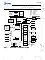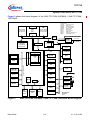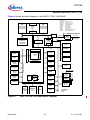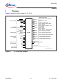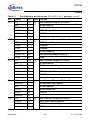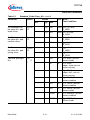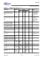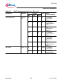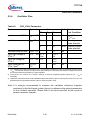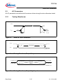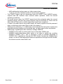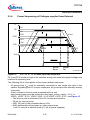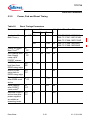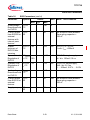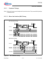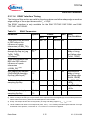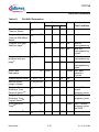
1
32-Bit
Microcontroller
TC1724
32-Bit Single-Chip Microcontroller
Data Sheet
V1.2 2014-06
Microcontrollers
Edition 2014-06
Published by
Infineon Technologies AG
81726 Munich, Germany
© 2014 Infineon Technologies AG
All Rights Reserved.
Legal Disclaimer
The information given in this document shall in no event be regarded as a guarantee of conditions or
characteristics. With respect to any examples or hints given herein, any typical values stated herein and/or any
information regarding the application of the device, Infineon Technologies hereby disclaims any and all warranties
and liabilities of any kind, including without limitation, warranties of non-infringement of intellectual property rights
of any third party.
Information
For further information on technology, delivery terms and conditions and prices, please contact the nearest
Infineon Technologies Office (www.infineon.com).
Warnings
Due to technical requirements, components may contain dangerous substances. For information on the types in
question, please contact the nearest Infineon Technologies Office.
Infineon Technologies components may be used in life-support devices or systems only with the express written
approval of Infineon Technologies, if a failure of such components can reasonably be expected to cause the failure
of that life-support device or system or to affect the safety or effectiveness of that device or system. Life support
devices or systems are intended to be implanted in the human body or to support and/or maintain and sustain
and/or protect human life. If they fail, it is reasonable to assume that the health of the user or other persons may
be endangered.
32-Bit
Microcontroller
TC1724
32-Bit Single-Chip Microcontroller
Data Sheet
V1.2 2014-06
Microcontrollers
TC1724
Table of Contents
Table of Contents
1
Summary of Features . . . . . . . . . . . . . . . . . . . . . . . . . . . . . . . . . . . . . . 1-1
2
2.1
System Overview of the TC1724 . . . . . . . . . . . . . . . . . . . . . . . . . . . . . 2-1
Block Diagrams . . . . . . . . . . . . . . . . . . . . . . . . . . . . . . . . . . . . . . . . . . . . 2-2
3
Pinning . . . . . . . . . . . . . . . . . . . . . . . . . . . . . . . . . . . . . . . . . . . . . . . . . . 3-1
4
Identification Registers . . . . . . . . . . . . . . . . . . . . . . . . . . . . . . . . . . . . . 4-1
5
5.1
5.1.1
5.1.2
5.1.3
5.1.4
5.1.5
5.2
5.2.1
5.2.2
5.2.3
5.2.4
5.2.5
5.2.5.1
5.3
5.3.1
5.3.2
5.3.3
5.3.4
5.3.5
5.3.6
5.3.7
5.3.8
5.3.9
5.3.10
5.3.11
5.3.11.1
5.3.11.2
5.3.11.3
5.3.11.4
5.4
5.4.1
5.4.2
Electrical Parameters . . . . . . . . . . . . . . . . . . . . . . . . . . . . . . . . . . . . . . 5-1
General Parameters . . . . . . . . . . . . . . . . . . . . . . . . . . . . . . . . . . . . . . . . 5-1
Parameter Interpretation . . . . . . . . . . . . . . . . . . . . . . . . . . . . . . . . . . . 5-1
Pad Driver and Pad Classes Summary . . . . . . . . . . . . . . . . . . . . . . . . 5-2
Absolute Maximum Ratings . . . . . . . . . . . . . . . . . . . . . . . . . . . . . . . . . 5-3
Pin Reliability in Overload . . . . . . . . . . . . . . . . . . . . . . . . . . . . . . . . . . 5-5
Operating Conditions . . . . . . . . . . . . . . . . . . . . . . . . . . . . . . . . . . . . . . 5-7
DC Parameters . . . . . . . . . . . . . . . . . . . . . . . . . . . . . . . . . . . . . . . . . . . 5-11
Input/Output Pins . . . . . . . . . . . . . . . . . . . . . . . . . . . . . . . . . . . . . . . . 5-11
Analog to Digital Converters (ADCx) . . . . . . . . . . . . . . . . . . . . . . . . . 5-23
Fast Analog to Digital Converter (FADC) . . . . . . . . . . . . . . . . . . . . . . 5-34
Oscillator Pins . . . . . . . . . . . . . . . . . . . . . . . . . . . . . . . . . . . . . . . . . . 5-39
Power Supply Current . . . . . . . . . . . . . . . . . . . . . . . . . . . . . . . . . . . . 5-40
Calculating the 1.3 V Current Consumption . . . . . . . . . . . . . . . . . 5-45
AC Parameters . . . . . . . . . . . . . . . . . . . . . . . . . . . . . . . . . . . . . . . . . . . 5-47
Testing Waveforms . . . . . . . . . . . . . . . . . . . . . . . . . . . . . . . . . . . . . . 5-47
Power Sequencing 5V Supply Only . . . . . . . . . . . . . . . . . . . . . . . . . . 5-48
Power Sequencing 3.3V Supply Only . . . . . . . . . . . . . . . . . . . . . . . . 5-50
Power Sequencing all Voltages supplied from External . . . . . . . . . . 5-52
Power, Pad and Reset Timing . . . . . . . . . . . . . . . . . . . . . . . . . . . . . . 5-54
EVR Parameter . . . . . . . . . . . . . . . . . . . . . . . . . . . . . . . . . . . . . . . . . 5-57
Phase Locked Loop (PLL) . . . . . . . . . . . . . . . . . . . . . . . . . . . . . . . . . 5-60
ERAY Phase Locked Loop (ERAY_PLL) . . . . . . . . . . . . . . . . . . . . . . 5-62
JTAG Interface Timing . . . . . . . . . . . . . . . . . . . . . . . . . . . . . . . . . . . . 5-63
DAP Interface Timing . . . . . . . . . . . . . . . . . . . . . . . . . . . . . . . . . . . . . 5-65
Peripheral Timings . . . . . . . . . . . . . . . . . . . . . . . . . . . . . . . . . . . . . . . 5-67
Micro Link Interface (MLI) Timing . . . . . . . . . . . . . . . . . . . . . . . . . 5-67
Micro Second Channel (MSC) Interface Timing . . . . . . . . . . . . . . 5-69
SSC Master/Slave Mode Timing . . . . . . . . . . . . . . . . . . . . . . . . . . 5-72
ERAY Interface Timing . . . . . . . . . . . . . . . . . . . . . . . . . . . . . . . . . 5-75
Package and Reliability . . . . . . . . . . . . . . . . . . . . . . . . . . . . . . . . . . . . . 5-77
Package Parameters . . . . . . . . . . . . . . . . . . . . . . . . . . . . . . . . . . . . . 5-77
Package Outline . . . . . . . . . . . . . . . . . . . . . . . . . . . . . . . . . . . . . . . . 5-78
Data Sheet
I-1
V1.2, 2014-06
TC1724
Table of Contents
5.4.3
5.4.4
5.5
Data Sheet
Flash Memory Parameters . . . . . . . . . . . . . . . . . . . . . . . . . . . . . . . . 5-78
Quality Declarations . . . . . . . . . . . . . . . . . . . . . . . . . . . . . . . . . . . . . . 5-80
Revision History . . . . . . . . . . . . . . . . . . . . . . . . . . . . . . . . . . . . . . . . . . . 5-81
I-2
V1.2, 2014-06
TC1724
Summary of Features
1
Summary of Features
The SAK-TC1724F-192F133HL / SAK-TC1724F-192F133HR has the following
features:
•
•
•
•
•
•
•
High-performance 32-bit super-scalar TriCore V1.3.1 CPU with 4-stage pipeline
– Superior real-time performance
– Strong bit handling
– Fully integrated DSP capabilities
– Single precision Floating Point Unit (FPU)
– 133 MHz operation at full temperature range
32-bit Peripheral Control Processor with single cycle instruction (PCP2)
– 8 Kbyte Parameter Memory (PRAM)
– 24 Kbyte Code Memory (CMEM)
– 133 MHz operation at full temperature range
Multiple on-chip memories
– 1.5 Mbyte Program Flash Memory (PFLASH) with ECC
– 64 Kbyte Data Flash Memory (DFLASH) usable for EEPROM emulation
– 120 Kbyte Data Memory (LDRAM)
– Instruction Cache: up to 8Kbyte (ICACHE, configurable)
– 24 Kbyte Code Scratchpad Memory (SPRAM)
– Data Cache: up to 4 Kbyte (DCACHE, configurable)
– 8 Kbyte Overlay Memory (OVRAM)
– 16 Kbyte BootROM (BROM)
16-Channel DMA Controller
Sophisticated interrupt system with 2 × 255 hardware priority arbitration levels
serviced by CPU or PCP2
High performing on-chip bus structure
– 64-bit Local Memory Buses between CPU, Flash and Data Memory
– 32-bit System Peripheral Bus (SPB) for on-chip peripheral and functional units
– One bus bridge (LFI Bridge)
Versatile On-chip Peripheral Units
– Two Asynchronous/Synchronous Serial Channels (ASC) with baud rate generator,
parity, framing and overrun error detection
– Four High-Speed Synchronous Serial Channels (SSC) with programmable data
length and shift direction
– One serial Micro Second Bus interface (MSC) for serial port expansion to external
power devices
– One High-Speed Micro Link interface (MLI) for serial inter-processor
communication
– One MultiCAN Module with 3 CAN nodes and 64 free assignable message objects
for high efficiency data handling via FIFO buffering and gateway data transfer
– One FlexRayTM module with 2 channels (E-Ray).
Data Sheet
1-1
V1.2, 2014-06
TC1724
Summary of Features
•
•
•
•
•
•
•
•
– One General Purpose Timer Array Module (GPTA) providing a powerful set of
digital signal filtering and timer functionality to realize autonomous and complex
Input/Output management
– Two Capture/Compare Unit 6 (CAPCOM6) kernels
– Two General Purpose Timer (GPT12) modules
28 analog input lines for ADC
– 2 independent kernels (ADC0 and ADC1)
– Analog supply voltage range from 3.3 V to 5 V (single supply)
– Broken wire detection
2 different FADC input channels
– channels with impedance control and overlaid with ADC1 inputs
– Extreme fast conversion, 21 cycles of fFADC clock
– 10-bit A/D conversion (higher resolution can be achieved by averaging of
consecutive conversions in digital data reduction filter)
95 digital general purpose I/O lines (GPIO)
Digital I/O ports with 3.3 V capability
On-chip debug support for OCDS Level 1 (CPU, PCP, DMA, On Chip Bus)
Dedicated Emulation Device chip available (TC1724ED)
– multi-core debugging, real time tracing, and calibration
– four/five wire JTAG (IEEE 1149.1) or two wire DAP (Device Access Port) interface
Power Management System
Clock Generation Unit with PLL
Data Sheet
1-2
V1.2, 2014-06
TC1724
Summary of Features
The SAK-TC1724N-192F133HR has the following features:
•
•
•
•
•
•
•
High-performance 32-bit super-scalar TriCore V1.3.1 CPU with 4-stage pipeline
– Superior real-time performance
– Strong bit handling
– Fully integrated DSP capabilities
– Single precision Floating Point Unit (FPU)
– 133 MHz operation at full temperature range
32-bit Peripheral Control Processor with single cycle instruction (PCP2)
– 8 Kbyte Parameter Memory (PRAM)
– 24 Kbyte Code Memory (CMEM)
– 133 MHz operation at full temperature range
Multiple on-chip memories
– 1.5 Mbyte Program Flash Memory (PFLASH) with ECC
– 64 Kbyte Data Flash Memory (DFLASH) usable for EEPROM emulation
– 120 Kbyte Data Memory (LDRAM)
– Instruction Cache: up to 8Kbyte (ICACHE, configurable)
– 24 Kbyte Code Scratchpad Memory (SPRAM)
– Data Cache: up to 4 Kbyte (DCACHE, configurable)
– 8 Kbyte Overlay Memory (OVRAM)
– 16 Kbyte BootROM (BROM)
16-Channel DMA Controller
Sophisticated interrupt system with 2 × 255 hardware priority arbitration levels
serviced by CPU or PCP2
High performing on-chip bus structure
– 64-bit Local Memory Buses between CPU, Flash and Data Memory
– 32-bit System Peripheral Bus (SPB) for on-chip peripheral and functional units
– One bus bridge (LFI Bridge)
Versatile On-chip Peripheral Units
– Two Asynchronous/Synchronous Serial Channels (ASC) with baud rate generator,
parity, framing and overrun error detection
– Four High-Speed Synchronous Serial Channels (SSC) with programmable data
length and shift direction
– One serial Micro Second Bus interface (MSC) for serial port expansion to external
power devices
– One High-Speed Micro Link interface (MLI) for serial inter-processor
communication
– One MultiCAN Module with 3 CAN nodes and 64 free assignable message objects
for high efficiency data handling via FIFO buffering and gateway data transfer
– One General Purpose Timer Array Module (GPTA) providing a powerful set of
digital signal filtering and timer functionality to realize autonomous and complex
Input/Output management
– Two Capture/Compare Unit 6 (CAPCOM6) kernels
Data Sheet
1-3
V1.2, 2014-06
TC1724
Summary of Features
•
•
•
•
•
•
•
•
– Two General Purpose Timer (GPT12) modules
28 analog input lines for ADC
– 2 independent kernels (ADC0 and ADC1)
– Analog supply voltage range from 3.3 V to 5 V (single supply)
2 different FADC input channels
– channels with impedance control and overlaid with ADC1 inputs
– Extreme fast conversion, 21 cycles of fFADC clock
– 10-bit A/D conversion (higher resolution can be achieved by averaging of
consecutive conversions in digital data reduction filter)
95 digital general purpose I/O lines (GPIO)
Digital I/O ports with 3.3 V capability
On-chip debug support for OCDS Level 1 (CPU, PCP, DMA, On Chip Bus)
Dedicated Emulation Device chip available (TC1724ED)
– multi-core debugging, real time tracing, and calibration
– four/five wire JTAG (IEEE 1149.1) or two wire DAP (Device Access Port) interface
Power Management System
Clock Generation Unit with PLL
Data Sheet
1-4
V1.2, 2014-06
TC1724
Summary of Features
The SAK-TC1724N-192F80HL / SAK-TC1724N-192F80HR has the following features:
•
•
•
•
•
•
•
High-performance 32-bit super-scalar TriCore V1.3.1 CPU with 4-stage pipeline
– Superior real-time performance
– Strong bit handling
– Fully integrated DSP capabilities
– Single precision Floating Point Unit (FPU)
– 80 MHz operation at full temperature range
32-bit Peripheral Control Processor with single cycle instruction (PCP2)
– 8 Kbyte Parameter Memory (PRAM)
– 24 Kbyte Code Memory (CMEM)
– 80 MHz operation at full temperature range
Multiple on-chip memories
– 1.5 Mbyte Program Flash Memory (PFLASH) with ECC
– 64 Kbyte Data Flash Memory (DFLASH) usable for EEPROM emulation
– 120 Kbyte Data Memory (LDRAM)
– Instruction Cache: up to 8Kbyte (ICACHE, configurable)
– 24 Kbyte Code Scratchpad Memory (SPRAM)
– Data Cache: up to 4 Kbyte (DCACHE, configurable)
– 8 Kbyte Overlay Memory (OVRAM)
– 16 Kbyte BootROM (BROM)
16-Channel DMA Controller
Sophisticated interrupt system with 2 × 255 hardware priority arbitration levels
serviced by CPU or PCP2
High performing on-chip bus structure
– 64-bit Local Memory Buses between CPU, Flash and Data Memory
– 32-bit System Peripheral Bus (SPB) for on-chip peripheral and functional units
– One bus bridge (LFI Bridge)
Versatile On-chip Peripheral Units
– Two Asynchronous/Synchronous Serial Channels (ASC) with baud rate generator,
parity, framing and overrun error detection
– Four High-Speed Synchronous Serial Channels (SSC) with programmable data
length and shift direction
– One serial Micro Second Bus interface (MSC) for serial port expansion to external
power devices
– One High-Speed Micro Link interface (MLI) for serial inter-processor
communication
– One MultiCAN Module with 3 CAN nodes and 64 free assignable message objects
for high efficiency data handling via FIFO buffering and gateway data transfer
– One General Purpose Timer Array Module (GPTA) providing a powerful set of
digital signal filtering and timer functionality to realize autonomous and complex
Input/Output management
– Two Capture/Compare Unit 6 (CAPCOM6) kernels
Data Sheet
1-5
V1.2, 2014-06
TC1724
Summary of Features
•
•
•
•
•
•
•
•
– Two General Purpose Timer (GPT12) modules
28 analog input lines for ADC
– 2 independent kernels (ADC0 and ADC1)
– Analog supply voltage range from 3.3 V to 5 V (single supply)
2 different FADC input channels
– channels with impedance control and overlaid with ADC1 inputs
– Extreme fast conversion, 21 cycles of fFADC clock
– 10-bit A/D conversion (higher resolution can be achieved by averaging of
consecutive conversions in digital data reduction filter)
95 digital general purpose I/O lines (GPIO)
Digital I/O ports with 3.3 V capability
On-chip debug support for OCDS Level 1 (CPU, PCP, DMA, On Chip Bus)
Dedicated Emulation Device chip available (TC1724ED)
– multi-core debugging, real time tracing, and calibration
– four/five wire JTAG (IEEE 1149.1) or two wire DAP (Device Access Port) interface
Power Management System
Clock Generation Unit with PLL
Data Sheet
1-6
V1.2, 2014-06
TC1724
Summary of Features
Ordering Information
The ordering code for Infineon microcontrollers provides an exact reference to the
required product. This ordering code identifies:
•
•
The derivative itself, i.e. its function set, the temperature range, and the supply
voltage
The package and the type of delivery.
For the available ordering codes for the TC1724 please refer to the “Product Catalog
Microcontrollers”, which summarizes all available microcontroller variants.
This document describes the derivatives of the device.The Table 1 enumerates these
derivatives and summarizes the differences.
Table 1
TC1724 Derivative Synopsis
Derivative
CPU/PCP Flash
Ambient
Size
Temperatur Freq.
e Range (TA)
ERAY Wire
Bond
Material
SAK-TC1724F-192F133HL
-40oC to
+125oC
133 MHz
1.5 MB
Yes
Au
SAK-TC1724F-192F133HR1)
-40oC to
+125oC
133 MHz
1.5 MB
Yes
Cu
SAK-TC1724N-192F133HR
-40oC to
+125oC
133 MHz
1.5 MB
No
Cu
SAK-TC1724N-192F80HL
-40oC to
+125oC
80 MHz
1.5 MB
No
Au
SAK-TC1724N-192F80HR2)
-40oC to
+125oC
80 MHz
1.5 MB
No
Cu
1) This derivative has the same features as the SAK-TC1724F-192F133HL, except the wire-bonding material.
2) This derivative has the same features as the SAK-TC1724N-192F80HL, except the wire-bonding material.
Data Sheet
1-7
V1.2, 2014-06
TC1724
System Overview of the TC1724
2
System Overview of the TC1724
The TC1724 combines three powerful technologies within one silicon die, achieving new
levels of power, speed, and economy for embedded applications:
•
•
•
Reduced Instruction Set Computing (RISC) processor architecture
Digital Signal Processing (DSP) operations and addressing modes
On-chip memories and peripherals
DSP operations and addressing modes provide the computational power necessary to
efficiently analyze complex real-world signals. The RISC load/store architecture
provides high computational bandwidth with low system cost. On-chip memory and
peripherals are designed to support even the most demanding high-bandwidth real-time
embedded control-systems tasks.
Additional high-level features of the TC1724 include:
•
•
•
•
•
•
•
•
•
Efficient memory organization: instruction and data scratch memories, caches
Serial communication interfaces – flexible synchronous and asynchronous modes
Peripheral Control Processor – standalone data operations and interrupt servicing
DMA Controller – DMA operations and interrupt servicing
General-purpose timers
High-performance on-chip buses
On-chip debugging and emulation facilities
Flexible interconnections to external components
Flexible power-management
The TC1724 is a high-performance microcontroller with TriCore CPU, program and data
memories, buses, bus arbitration, an interrupt controller, a peripheral control processor
and a DMA controller and several on-chip peripherals. The TC1724 is designed to meet
the needs of the most demanding embedded control systems applications where the
competing issues of price/performance, real-time responsiveness, computational power,
data bandwidth, and power consumption are key design elements.
The TC1724 offers several versatile on-chip peripheral units such as serial controllers,
timer units, CAPCOM6 and Analog-to-Digital converters. Within the TC1724, all these
peripheral units are connected to the TriCore CPU/system via the Flexible Peripheral
Interconnect (FPI) Bus and the Local Memory Bus (LMB). Several I/O lines on the
TC1724 ports are reserved for these peripheral units to communicate with the external
world.
Data Sheet
2-1
V1.2, 2014-06
TC1724
System Overview of the TC1724
2.1
Block Diagrams
Figure 1 shows the block diagram of the SAK-TC1724F-192F133HL / SAK-TC1724F192F133HR.
Abbreviations:
ICACHE:
Instruction Cache
DCACHE Data Cache
SPRAM:
Scratch-Pad RAM
LDRAM:
Local Data RAM
OVRAM:
Overlay RAM
BROM:
Boot ROM
PFlash:
Program Flash
DFlash:
Data Flash
PRAM:
Parameter RAM in PCP
CMEM:
Code RAM in PCP
FPU
PMI
DMI
TriCore
CPU
16 KB SPRAM
8 KB ICACHE
(Configurable)
116 KB LDRAM
4 KB DCACHE
(Configurable)
TC1.3.1
133MHz
CPS
Local Memory Bus
1.3V, 3.3V
Int. Supply
DMA
LFI Bridge
16 channels
EVR
Embedded
Voltage
Regulator
5V, 3.3V
Single-source
Ext. Supply
SMIF
M
PMU
1,5 MB PFlash
64 KB Dflash
16 KB BROM
8 KB OVRAM
Optional Ext. Supply
LBCU
(LMB)
M/S
OCDS L1 Debug
Interface
ASC0
ASC1
PCP2
Core
JTAG/DAP
Interrupt
System
MLI0
Interrupts
FPI-Bus Interface
8 KB PRAM
System Peripheral Bus
(SPB)
STM
MemCheck
24 KB CMEM
SCU
CAPCOM
(CCU60, CCU61)
GPT12
(GPT 120)
System Peripheral Bus
E-Ray
(2 channels)
FCE
Ports
5V
Ext. ADC Supply
BMU
ADC0
GPT12
(GPT 121)
SBCU
PLL
E-RAY
fE -Ray
PLL
fCPU
SSC0
(5V max,
16 channels )
16
ADC1
8
(5V max,
24 channels )
4
SSC1
GPTA 0
FADC
(3.3V max,
2 differential
SSC2
Ext.
Request
Unit
Figure 1
Data Sheet
MultiCAN
(3 Nodes,
64 MO)
MSC0
SSC3
channels )
BlockDiagram
TC1724F
V0.8
SAK-TC1724F-192F133HL / SAK-TC1724F-192F133HR Block
Diagram
2-2
V1.2, 2014-06
TC1724
System Overview of the TC1724
Figure 2 shows the block diagram of the SAK-TC1724N-192F133HR.
Abbreviations:
ICACHE:
Instruction Cache
DCACHE
Data Cache
SPRAM:
Scratch-Pad RAM
LDRAM:
Local Data RAM
OVRAM:
Overlay RAM
BROM:
Boot ROM
PFlash:
Program Flash
DFlash:
Data Flash
PRAM:
Parameter RAM in PCP
CMEM:
Code RAM in PCP
FPU
PMI
DMI
TriCore
CPU
16 KB SPRAM
8 KB ICACHE
(Configurable)
116 KB LDRAM
4 KB DCACHE
(Configurable)
TC1.3.1
133MHz
CPS
Local Memory Bus
1.3V, 3.3V
Int. Supply
DMA
LFI Bridge
16 channels
EVR
Embedded
Voltage
Regulator
5V, 3.3V
Single-source
Ext. Supply
SMIF
M
PMU
1,5 MB PFlash
64 KB Dflash
16 KB BROM
8 KB OVRAM
Optional Ext. Supply
LBCU
(LMB)
M/S
OCDS L1 Debug
Interface
ASC0
ASC1
System Peripheral Bus
(SPB)
JTAG/DAP
Interrupt
System
MLI0
Interrupts
FPI-Bus Interface
8 KB PRAM
PCP2
Core
STM
MemCheck
24 KB CMEM
CAPCOM
(CCU60, CCU61)
GPT12
(GPT 120)
System Peripheral Bus
SCU
FCE
Ports
5V
Ext. ADC Supply
BMU
ADC0
GPT12
(GPT 121)
SSC0
SBCU
PLL
fCPU
(5V max,
16 channels )
16
ADC1
8
(5V max,
24 channels )
4
SSC1
GPTA 0
FADC
(3.3V max,
2 differential
SSC2
Ext.
Request
Unit
Figure 2
Data Sheet
MultiCAN
(3 Nodes,
64 MO)
MSC0
SSC3
channels )
BlockDiagram
TC1724N
V0.8
SAK-TC1724N-192F133HR Block Diagram
2-3
V1.2, 2014-06
TC1724
System Overview of the TC1724
Figure 3 shows the block diagram of the SAK-TC1724N-192F80HL / SAK-TC1724N192F80HR.
Abbreviations:
ICACHE:
Instruction Cache
DCACHE
Data Cache
SPRAM:
Scratch-Pad RAM
LDRAM:
Local Data RAM
OVRAM:
Overlay RAM
BROM:
Boot ROM
PFlash:
Program Flash
DFlash:
Data Flash
PRAM:
Parameter RAM in PCP
CMEM:
Code RAM in PCP
FPU
PMI
DMI
TriCore
CPU
16 KB SPRAM
8 KB ICACHE
(Configurable)
116 KB LDRAM
4 KB DCACHE
(Configurable)
TC1.3.1
80MHz
CPS
Local Memory Bus
1.3V, 3.3V
Int. Supply
DMA
LFI Bridge
16 channels
EVR
Embedded
Voltage
Regulator
5V, 3.3V
Single-source
Ext. Supply
SMIF
M
PMU
1,5 MB PFlash
64 KB Dflash
16 KB BROM
8 KB OVRAM
Optional Ext. Supply
LBCU
(LMB)
M/S
OCDS L1 Debug
Interface
ASC0
ASC1
System Peripheral Bus
(SPB)
JTAG/DAP
Interrupt
System
MLI0
Interrupts
FPI-Bus Interface
8 KB PRAM
PCP2
Core
STM
MemCheck
24 KB CMEM
CAPCOM
(CCU60, CCU61)
GPT12
(GPT 120)
System Peripheral Bus
SCU
FCE
Ports
5V
Ext. ADC Supply
BMU
ADC0
GPT12
(GPT 121)
SSC0
SBCU
PLL
fCPU
ADC1
8
(5V max,
24 channels )
4
FADC
SSC2
Ext.
Request
Unit
Data Sheet
16
SSC1
GPTA 0
Figure 3
(5V max,
16 channels )
MultiCAN
(3 Nodes,
64 MO)
MSC0
SSC3
(3.3V max,
2 differential
channels )
BlockDiagram
TC1724N
V0.8
SAK-TC1724N-192F80HL / SAK-TC1724N-192F80HR Block Diagram
2-4
V1.2, 2014-06
TC1724
System Overview of the TC1724
Figure 4 shows the block diagram of the SAK-TC1724F-192F80HR.
Abbreviations:
ICACHE:
Instruction Cache
DCACHE Data Cache
SPRAM:
Scratch-Pad RAM
LDRAM:
Local Data RAM
OVRAM:
Overlay RAM
BROM:
Boot ROM
PFlash:
Program Flash
DFlash:
Data Flash
PRAM:
Parameter RAM in PCP
CMEM:
Code RAM in PCP
FPU
PMI
DMI
TriCore
CPU
16 KB SPRAM
8 KB ICACHE
(Configurable)
116 KB LDRAM
4 KB DCACHE
(Configurable)
TC1.3.1
80MHz
CPS
Local Memory Bus
1.3V, 3.3V
Int. Supply
DMA
LFI Bridge
16 channels
EVR
Embedded
Voltage
Regulator
5V, 3.3V
Single-source
Ext. Supply
SMIF
M
PMU
1,5 MB PFlash
64 KB Dflash
16 KB BROM
8 KB OVRAM
Optional Ext. Supply
LBCU
(LMB)
M/S
OCDS L1 Debug
Interface
ASC0
ASC1
PCP2
Core
System Peripheral Bus
(SPB)
JTAG/DAP
Interrupt
System
MLI0
Interrupts
FPI-Bus Interface
8 KB PRAM
STM
MemCheck
24 KB CMEM
SCU
CAPCOM
(CCU60, CCU61)
GPT12
(GPT 120)
System Peripheral Bus
E-Ray
(2 channels)
FCE
Ports
5V
Ext. ADC Supply
BMU
ADC0
GPT12
(GPT 121)
SBCU
PLL
E-RAY
fE -Ray
PLL
fCPU
SSC0
8
(5V max,
24 channels )
4
FADC
SSC2
Ext.
Request
Unit
Data Sheet
16
ADC1
SSC1
GPTA 0
Figure 4
(5V max,
16 channels )
MultiCAN
(3 Nodes,
64 MO)
MSC0
SSC3
(3.3V max,
2 differential
channels )
BlockDiagram
TC1724F
V0.8
SAK-TC1724F-192F80HR Block Diagram
2-5
V1.2, 2014-06
TC1724
Pinning
3
Pinning
Figure 5 shows the logic symbol for TC1724
Alternate Functions
General Control
12
PORST
TESTMODE
ESR0
ESR1
9
14
OCDS /
JTAG Control
Analog Inputs
Analog Power
Supply
2
TMS / DAP1
16
VD D
VD D P
VSS
EVR Pass
Device Gate
Figure 5
Data Sheet
V PD G
Port 4
Port 5
9
TC172 4
9
V DD M
VSSM
V AR EF0
VAGN D 0
V5
Digital Circuitry
Power Supply
Port 3
TCK / DAP0
AN[16:0],
AN19, AN23,
AN25,
AN[39:32]
Port 1
Port 2
16
TRST
Port 0
4
4
GPTA, SCU, E-RAY1), MSC0,
CCU6
SCU, GPTA, SSC1,
OCDS, CCU6, GPT12
GPTA, SSC0/1, MSC0, MLI0,
CCU6, GPT12
GPTA, ASC0/1, SSC0/1, SCU,
CAN, MSC0
GPTA, SCU,
CCU6, GPT12
GPTA, E-RAY 1), SSC0/2, CAN,
CCU6, GPT12, SCU, ADC1
Port 8
CCU6, GPT12, SSC3, GPTA
Port 9
GPTA, CCU6, CAN, OCDS/JTAG
Port 11
Overlaid digital /analog inputs
Port 12
Overlaid digital /analog inputs
XTAL1
XTAL2
Oscillator
4
5
4
2
1 )On ly a va ila b le fo r
1
SAK -TC 1 7 2 4F-1 9 2F1 3 3H L, SAK- TC1 7 2 4F-1 9 2F13 3HR
TC1724_LogSym_144
TC1724 Logic Symbol
3-1
V1.2, 2014-06
TC1724
1
2
3
4
5
6
7
8
9
10
11
12
13
14
15
16
17
18
19
20
21
22
23
24
25
26
27
28
29
30
31
32
33
34
35
36
TC1724
108
107
106
105
104
103
102
101
100
99
98
97
96
95
94
93
92
91
90
89
88
87
86
85
84
83
82
81
80
79
78
77
76
75
74
73
P3.4/MTSR0/OUT88
P3.7/SLSO02/SLSO12/SLSI0/OUT89
P3.3/MRST0/OUT87
P3.2/SCLK0/OUT86
P3.8/SLSO06/TXD1/OUT90/REQ14
P3.6/SLSO01/SLSO11/SLSOANDO1
P3.5/SLSO00/SLSO10/SLSOANDO0
P8.13/OUT4/COUT60
P8.3/SLSI3/CC61INC/CC61/OUT51/SLSO30
P8.4/OUT99/COUT62/SLSO31
ESR0
PORST
ESR1
P1.1/IN17/OUT17/OUT73/T13HRE/CTRAPB
TESTMODE
P1.15/BRKIN/BRKOUT
P1.0/REQ15/IN16/OUT16/OUT72/T3OUT/BRKIN/BRKOUT
TCK/DAP0
TRST
P9.6/TDO/BRKIN/BRKOUT
TMS/DAP1
P9.5/TDI/BRKIN/BRKOUT
V5
V DDP
V DD
V SS
XTAL2
XTAL1
VSS
P1.4/IN20/EMGSTOP/OUT20/OUT76/COUT61
P1.3/IN19/OUT19/OUT75/COUT63
P1.11/IN27/IN51/SCLK1B/OUT27/OUT51/CCPOS0C/T2INA/B
P1.10/IN26/IN50/OUT26/OUT50/SLSO17
P1.9/IN25/IN49/MRST1B/OUT25/OUT49/CCPOS1C/T2EUDA/B
P1.8/IN24/IN48/MTSR1B/OUT24/OUT48/CCPOS2C/T4EUDA/B
P4.3/IN31/IN55/OUT31/OUT55/EXTCLK0/T12HRE/CTRAPA
AN19/DIG3/P11.3
AN16/DIG0/P11.0
AN15
AN14
VAGND0
VAREF0
VSSM
VDDM
AN13
AN12
AN11
AN10
AN9
AN8
AN6
AN5
AN4
AN3
AN2
AN1
AN0
VDD
VDDP
V5
CC62/CC62INA/B/TCLK0/OUT32/IN32/P2.0
CCPOS0A/T12HRB/T2INA/B/SLSO13/SLSO03/OUT33/TREADY0A/IN33/P2.1
CC61/CC61INA/B/TVALID0A/OUT34/IN34/P2.2
T12HRC/T13HRC/CCPOS2A/T4EUDA/B/TDATA0/OUT35/IN35/P2.3
COUT63/OUT36/RCLK0A/IN36/P2.4
CC60/CC60INA/B/RREADY0A/OUT37/IN37/P2.5
COUT62/OUT38/RVALID0A/IN38/P2.6
COUT60/OUT39/RDATA0A/IN39/P2.7
SLSO32/OUT100/CC60/CC60INC/P8.5
COUT61/OUT101/P8.6
CC62INC/CC62/OUT102/P8.7
T13HRB/CCPOS1A/T2EUDA/B/EXTCLK1/OUT54/OUT30/IN54/IN30/P4.2
37
38
39
40
41
42
43
44
45
46
47
48
49
50
51
52
53
54
55
56
57
58
59
60
61
62
63
64
65
66
67
68
69
70
71
72
REQ7/CC62/CC62INA/B/CAPINA/B/SLSO20/OUT40/IN40/P5.0
SLSO21/OUT41/IN41/P5.1
COUT62/SLSO22/OUT42/IN42/P5.2
SLSO23/OUT43/IN43/P5.3
RXDCAN 2/OUT80/P9.0
TXDCAN2/OUT81/P9.1
SLSI2A/SLSO24/OUT44/IN44/P5.4
MRST2A/OUT45/IN45/P5.5
MTSR2A/OUT46/IN46/P5.6
SCLK2A/OUT47/IN47/P5.7
1)
TXDCAN0/OUT37/RXDB1 /P5.15
VDD
CC60INC/CC60/OUT87/P9.7
COUT60/OUT88/P9.8
1)
CC61/CC61INA/B/OUT6/TXDA1 /P5.8
1)
OUT7/RXDCAN0/TXDB1 /P5.9
COUT61/OUT8/TXENA 1)/P5.10
1)
COUT63/OUT9/TXENB /P5.11
CCPOS0A/T12HRB/T3INA/B/AD1EMUX0/SLSO07/OUT19/P5.12
CCPOS1A/T13HRB/T3EUDA/B/OUT20/AD1EMUX1/P5.13
CCPOS2A/T12HRC/T13HRC/T4INA/B/OUT36/AD1EMUX2/RXDA1 1)/P5.14
VDDP
1) VDD
V5
V PDG
AN39/DIG19/P12.3
AN38/DIG18/P12.2
AN37/DIG17/P12.1
AN36/DIG16/P12.0
AN35
AN34
AN33
AN32
AN7
AN25/DIG9/P11.9
AN23/DIG7/P11.7
144
143
142
141
140
139
138
137
136
135
134
133
132
131
130
129
128
127
126
125
124
123
122
121
120
119
118
117
116
115
114
113
112
111
110
109
P0.15/IN15/REQ5/OUT15/OUT71/COUT61
P0.14/IN14/REQ4/OUT14/OUT70/CC61INC/CC61
P0.7/IN7/REQ3/HWCFG7/OUT7/OUT63/EVTO3
P0.6/IN6/REQ2/HWCFG6/OUT6/OUT62/EVTO2
P9.2/COUT63/OUT82
P9.3/OUT83/COUT62
P9.4/CC62INC/CC62/OUT84
1)
P0.13/IN13/OUT13/TXENB /OUT69
1)
P0.12/IN12/OUT12/TXENA /OUT68/CTRAPB/T13HRE
P0.5/IN5/HWCFG5/OUT5/OUT61/EVTO1
P0.4/IN4/HWCFG4/OUT4/OUT60/EVTO0
P2.13/SLSI11/SDI0/CTRAPA/T12HRE/SLSO16/T6OUT
P2.8/SLSO04/SLSO14/EN00
P2.12/MTSR1A/SOP0B
P2.11/SCLK1A/FCLP0B
P2.10/MRST1A
P2.9/SLSO05/SLSO15/EN01
V5
VDDP
VDD
P0.3/IN3/HWCFG3/OUT3/OUT59
P0.2/IN2/HWCFG2/OUT2/OUT58
P0.1/IN1/HWCFG1/OUT1/OUT57/SDI1/COUT60
P0.0/IN0/HWCFG0/OUT0/OUT56/CC60/CC60INA/B
P3.11/REQ1/OUT93
P3.12/RXDCAN0/RXD0B/OUT94
P3.13/TXDCAN0/TXD0/OUT95
P8.0/SCLK3/CCPOS0C/T3INA/B/OUT48
P8.1/MRST3/CCPOS1C/T3EUDA/B/OUT49
P8.2/MTSR3/CCPOS2C/T4INA/B/OUT50
P3.9/RXD1A/OUT91
P3.10/REQ0/OUT92
P3.0/OUT84/RXD0A/REQ6
P3.1/TXD0/OUT85
P3.14/RXDCAN1/RXD1B/OUT96/SDI2
P3.15/TXDCAN1/TXD1/OUT97
Pinning
1) This pin is used as standby
power supply in emulation device.
1) Only available for
SAK-TC1724F-192F133HL, SAK-TC1724F-192F133HR
TC1724_QFP144
Figure 6
TC1724 Pinning for PG-LQFP-144-17 package
Table 3-1
Pin Definitions and Functions (PG-LQFP-144-17 package)
Pin
Symbol
Ctrl.
Type Function
Port 0
Data Sheet
3-2
V1.2, 2014-06
TC1724
Pinning
Table 3-1
Pin Definitions and Functions (PG-LQFP-144-17 package) (cont’d)
Pin
Symbol
Ctrl.
Type Function
121
P0.0
I/O0
A1/
PU
122
123
124
Port 0 General Purpose I/O Line 0
IN0
I
CCU60
I
CC60INA
CCU61
I
CC60INB
HWCFG0
I
Hardware Configuration Input 0
OUT0
O1
GPTA0 Output 0
OUT56
O2
GPTA0 Output 56
GPTA0 Input 0
CCU60
O3
P0.1
I/O0
IN1
I
SDI1
I
MSC0 Serial Data Input 1
HWCFG1
I
Hardware Configuration Input 1
OUT1
O1
GPTA0 Output 1
OUT57
O2
GPTA0 Output 57
CCU60
O3
COUT60
P0.2
I/O0
IN2
I
CC60
A1/
PU
A1/
PU
Port 0 General Purpose I/O Line 1
GPTA0 Input 1
Port 0 General Purpose I/O Line 2
GPTA0 Input 2
HWCFG2
I
Hardware Configuration Input 2
OUT2
O1
GPTA0 Output 2
OUT58
O2
GPTA0 Output 58
Reserved
O3
P0.3
I/O0
IN3
I
A1+/ Port 0 General Purpose I/O Line 3
PU
GPTA0 Input 3
HWCFG3
I
Hardware Configuration Input 3
OUT3
O1
GPTA0 Output 3
OUT59
O2
GPTA0 Output 59
Reserved
O3
-
Data Sheet
3-3
V1.2, 2014-06
TC1724
Pinning
Table 3-1
Pin Definitions and Functions (PG-LQFP-144-17 package) (cont’d)
Pin
Symbol
Ctrl.
Type Function
134
P0.4
I/O0
IN4
I
A1/
PD
HWCFG4
I
Hardware Configuration Input 4
OUT4
O1
GPTA0 Output 4
OUT60
O2
GPTA0 Output 60
EVTO0
O3
MCDS event output 0
P0.5
I/O0
IN5
I
HWCFG5
I
Hardware Configuration Input 5
OUT5
O1
GPTA0 Output 5
OUT61
O2
GPTA0 Output 61
EVTO1
O3
MCDS event output 1
135
141
142
P0.6
I/O0
IN6
I
HWCFG6
I
A1/
PD
A1/
PU
Port 0 General Purpose I/O Line 4
GPTA0 Input 4
Port 0 General Purpose I/O Line 5
GPTA0 Input 5
Port 0 General Purpose I/O Line 6
GPTA0 Input 6
Hardware Configuration Input 6
REQ2
I
External Request Input 2
OUT6
O1
GPTA0 Output 6
OUT62
O2
GPTA0 Output 62
EVTO2
O3
MCDS event output 2
P0.7
I/O0
IN7
I
HWCFG7
I
Hardware Configuration Input 7
REQ3
I
External Request Input 3
OUT7
O1
GPTA0 Output 7
OUT63
O2
GPTA0 Output 63
EVTO3
O3
MCDS event output 3
Data Sheet
A1/
PU
Port 0 General Purpose I/O Line 7
GPTA0 Input 7
3-4
V1.2, 2014-06
TC1724
Pinning
Table 3-1
Pin Definitions and Functions (PG-LQFP-144-17 package) (cont’d)
Pin
Symbol
Ctrl.
Type Function
136
P0.12
I/O0
IN12
I
A2/
PU
CCU60
I
CTRAPB
CCU61
I
T13HRE
OUT12
O1
GPTA0 Output 12
OUT68
O2
GPTA0 Output 68
TXENA
O3
E-Ray Channel A transmit Data Output
enable1)
P0.13
I/O0
IN13
I
OUT13
O1
GPTA0 Output 13
OUT69
O2
GPTA0 Output 69
TXENB
O3
E-Ray Channel B transmit Data Output
enable1)
P0.14
I/O0
IN14
I
REQ4
I
External Request Input 4
CCU61
I
CC61INC
OUT14
O1
GPTA0 Output 14
OUT70
O2
GPTA0 Output 70
CCU60
O3
CC61
137
143
144
P0.15
I/O0
IN15
I
A2/
PU
Port 0 General Purpose I/O Line 12
GPTA0 Input 12
Port 0 General Purpose I/O Line 13
GPTA0 Input 13
A1+/ Port 0 General Purpose I/O Line 14
PU
GPTA0 Input 14
A1+/ Port 0 General Purpose I/O Line 15
PU
GPTA0 Input 15
REQ5
I
External Request Input 5
OUT15
O1
GPTA0 Output 15
OUT71
O2
GPTA0 Output 71
CCU60
O3
COUT61
Port 1
Data Sheet
3-5
V1.2, 2014-06
TC1724
Pinning
Table 3-1
Pin Definitions and Functions (PG-LQFP-144-17 package) (cont’d)
Pin
Symbol
Ctrl.
Type Function
92
P1.0
I/O0
A2/
PU
95
78
79
Port 1 General Purpose I/O Line 0
REQ15
I
IN16
I
GPTA0 Input 16
BRKIN
I
Break Input
OUT16
O1
GPTA0 Output 16
OUT72
O2
GPTA0 Output 72
GPT120
O3
T3OUT
BRKOUT
O
P1.1
I/O0
IN17
I
CCU60
I
T13HRE
CCU61
I
CTRAPB
OUT17
O1
GPTA0 Output 17
OUT73
O2
GPTA0 Output 73
Reserved
O3
-
External Request Input 15
Break Output (controlled by OCDS module)
A1/
PU
A1/
PU
Port 1 General Purpose I/O Line 1
GPTA0 Input 17
P1.3
I/O0
IN19
I
OUT19
O1
GPTA0 Output 19
OUT75
O2
GPTA0 Output 75
CCU61
O3
COUT63
GPTA0 Input 19
P1.4
I/O0
IN20
I
EMGSTOP
I
Emergency Stop Input
OUT20
O1
GPTA0 Output 20
OUT76
O2
GPTA0 Output 76
CCU61
O3
COUT61
Data Sheet
A1/
PU
Port 1 General Purpose I/O Line 3
Port 1 General Purpose I/O Line 4
GPTA0 Input 20
3-6
V1.2, 2014-06
TC1724
Pinning
Table 3-1
Pin Definitions and Functions (PG-LQFP-144-17 package) (cont’d)
Pin
Symbol
Ctrl.
Type Function
74
P1.8
I/O0
IN24
I
A1+/ Port 1 General Purpose I/O Line 8
PU
GPTA0 Input 24
IN48
I
GPTA0 Input 48
MTSR1B
I
SSC1 Slave Receive Input B (Slave Mode)
CCU61
I
CCPOS2C
GPT120
I
T4EUDB
GPT121
I
T4EUDA
OUT24
O1
GPTA0 Output 24
OUT48
O2
GPTA0 Output 48
75
76
MTSR1B
O3
P1.9
I/O0
IN25
I
IN49
I
GPTA0 Input 49
MRST1B
I
SSC1 Master Receive Input B (Master Mode)
CCU61
I
CCPOS1C
GPT120
I
T2EUDB
GPT121
I
T2EUDA
OUT25
O1
GPTA0 Output 25
OUT49
O2
GPTA0 Output 49
MRST1B
O3
SSC1 Slave Transmit Output B (Slave Mode)
SSC1 Master Transmit Output B (Master Mode)
A1+/ Port 1 General Purpose I/O Line 9
PU
GPTA0 Input 25
P1.10
I/O0
IN26
I
IN50
I
GPTA0 Input 50
OUT26
O1
GPTA0 Output 26
OUT50
O2
GPTA0 Output 50
SLSO17
O3
SSC1 Slave Select Output 7
Data Sheet
A1+/ Port 1 General Purpose I/O Line 10
PU
GPTA0 Input 26
3-7
V1.2, 2014-06
TC1724
Pinning
Table 3-1
Pin Definitions and Functions (PG-LQFP-144-17 package) (cont’d)
Pin
Symbol
Ctrl.
Type Function
77
P1.11
I/O0
IN27
I
A1+/ Port 1 General Purpose I/O Line 11
PU
GPTA0 Input 27
IN51
I
GPTA0 Input 51
SCLK1B
I
SSC1 Clock Input B
CCU61
I
CCPOS0C
GPT120
I
T2INB
GPT121
I
T2INA
OUT27
O1
GPTA0 Output 27
OUT51
O2
GPTA0 Output 51
93
SCLK1B
O3
P1.15
I/O0
BRKIN
I
Reserved
O1
-
Reserved
O2
-
Reserved
O3
-
BRKOUT
O
Break Output (controlled by OCDS module)
SSC1 Clock Output B
A2/
PU
Port 1 General Purpose I/O Line 15
Break Input
Port 2
61
P2.0
I/O0
IN32
I
CCU60
I
CC62INB
CCU61
I
CC62INA
OUT32
O1
GPTA0 Output 32
TCLK0
O2
MLI0 Transmitter Clock Output 0
CCU61
O3
CC62
Data Sheet
A2/
PU
Port 2 General Purpose I/O Line 0
GPTA0 Input 32
3-8
V1.2, 2014-06
TC1724
Pinning
Table 3-1
Pin Definitions and Functions (PG-LQFP-144-17 package) (cont’d)
Pin
Symbol
Ctrl.
Type Function
62
P2.1
I/O0
IN33
I
A2/
PU
TREADY0A
I
MLI0 Transmitter Ready Input A
CCU61
I
CCPOS0A
CCU60
I
T12HRB
GPT120
I
T2INA
GPT121
I
T2INB
OUT33
O1
GPTA0 Output 33
SLSO03
O2
SSC0 Slave Select Output Line 3
63
64
Port 2 General Purpose I/O Line 1
GPTA0 Input 33
SLSO13
O3
P2.2
I/O0
IN34
I
CCU60
I
CC61INB
CCU61
I
CC61INA
OUT34
O1
GPTA0 Output 34
TVALID0A
O2
MLI0 Transmitter Valid Output
CCU61
O3
CC61
SSC1 Slave Select Output Line 3
A2/
PU
GPTA0 Input 34
P2.3
I/O0
IN35
I
CCU60
I
T12HRC
CCU60
I
T13HRC
CCU61
I
CCPOS2A
GPT120
I
T4EUDA
GPT121
I
T4EUDB
OUT35
O1
GPTA0 Output 35
TDATA0
O2
MLI0 Transmitter Data Output
Reserved
O3
-
Data Sheet
A2/
PU
Port 2 General Purpose I/O Line 2
Port 2 General Purpose I/O Line 3
GPTA0 Input 35
3-9
V1.2, 2014-06
TC1724
Pinning
Table 3-1
Pin Definitions and Functions (PG-LQFP-144-17 package) (cont’d)
Pin
Symbol
Ctrl.
Type Function
65
P2.4
I/O0
IN36
I
A2/
PU
RCLK0A
I
MLI Receiver Clock Input A
OUT36
O1
GPTA0 Output 36
CCU61
O2
COUT63
Reserved
O3
-
P2.5
I/O0
IN37
I
CCU60
I
CC60INB
CCU61
I
CC60INA
OUT37
O1
GPTA0 Output 37
RREADY0A
O2
MLI0 Receiver Ready Output A
CCU61
O3
P2.6
I/O0
IN38
I
RVALID0A
I
MLI Receiver Valid Input A
Reserved
I
-
OUT38
O1
GPTA0 Output 38
CCU61
O2
COUT62
Reserved
O3
-
66
67
68
132
A2/
PU
Port 2 General Purpose I/O Line 4
GPTA0 Input 36
Port 2 General Purpose I/O Line 5
GPTA0 Input 37
CC60
A2/
PU
A2/
PU
Port 2 General Purpose I/O Line 6
GPTA0 Input 38
P2.7
I/O0
RDATA0A
I
IN39
I
GPTA0 Input 39
OUT39
O1
GPTA0 Output 39
CCU61
O2
COUT60
Port 2 General Purpose I/O Line 7
MLI Receiver Data Input A
Reserved
O3
P2.8
I/O0
SLSO04
O1
SLSO14
O2
SSC1 Slave Select Output 4
EN00
O3
MSC0 Enable Output 0
Data Sheet
A2/
PU
Port 2 General Purpose I/O Line 8
SSC0 Slave Select Output 4
3-10
V1.2, 2014-06
TC1724
Pinning
Table 3-1
Pin Definitions and Functions (PG-LQFP-144-17 package) (cont’d)
Pin
Symbol
Ctrl.
Type Function
128
P2.9
I/O0
SLSO05
O1
A2/
PU
SLSO15
O2
SSC1 Slave Select Output 5
EN01
O3
MSC0 Enable Output 1
129
130
131
133
Port 2 General Purpose I/O Line 9
SSC0 Slave Select Output 5
P2.10
I/O0
MRST1A
I
A1+/ Port 2 General Purpose I/O Line 10
PU
SSC1 Master Receive Input A
MRST1A
O1
SSC1 Slave Transmit Output
Reserved
O2
-
Reserved
O3
-
P2.11
I/O0
SCLK1A
I
A1+/ Port 2 General Purpose I/O Line 11
PU
SSC1 Clock Input A
SCLK1A
O1
SSC1 Clock Output A
Reserved
O2
-
FCLP0B
O3
MSC0 Clock Output Positive B
P2.12
I/O0
MTSR1A
I
MTSR1A
O1
SSC1 Master Transmit Output A
Reserved
O2
-
SOP0B
O3
MSC0 Serial Data Output Positive B
P2.13
I/O0
SLSI11
I
SDI0
I
MSC0 Serial Data Input 0
CCU60
I
CTRAPA
CCU61
I
T12HRE
Reserved
O1
-
SLSO16
O2
SSC1 Slave Select Output 6
GPT120
O3
T6OUT
A1+/ Port 2 General Purpose I/O Line 12
PU
SSC1 Slave Receive Input A
A1+/ Port 2 General Purpose I/O Line 13
PU
SSC1 Slave Select Input 1
Port 3
Data Sheet
3-11
V1.2, 2014-06
TC1724
Pinning
Table 3-1
Pin Definitions and Functions (PG-LQFP-144-17 package) (cont’d)
Pin
Symbol
Ctrl.
Type Function
112
P3.0
I/O0
RXD0A
I
A1+/ Port 3 General Purpose I/O Line 0
PU
ASC0 Receiver Input A (Async. & Sync. Mode)
REQ6
I
External Request Input 6
RXD0A
O1
ASC0 Output (Sync. Mode)
Reserved
O2
-
OUT84
O3
GPTA0 Output 84
P3.1
I/O0
TXD0
O1
Reserved
O2
111
105
106
108
102
A1+/ Port 3 General Purpose I/O Line 1
PU
ASC0 Output
-
OUT85
O3
P3.2
I/O0
SCLK0
I
SCLK0
O1
SSC0 Clock Output (Master Mode)
Reserved
O2
-
OUT86
O3
GPTA0 Output 86
GPTA0 Output 85
A1+/ Port 3 General Purpose I/O Line 2
PU
SSC0 Clock Input (Slave Mode)
P3.3
I/O0
MRST0
I
A1+/ Port 3 General Purpose I/O Line 3
PU
SSC0 Master Receive Input (Master Mode)
MRST0
O1
SSC0 Slave Transmit Output (Slave Mode)
Reserved
O2
-
OUT87
O3
GPTA0 Output 87
P3.4
I/O0
MTSR0
I
A2/
PU
MTSR0
O1
SSC0 Master Transmit Output (Master Mode)
Reserved
O2
-
OUT88
O3
GPTA0 Output 88
Port 3 General Purpose I/O Line 4
SSC0 Slave Receive Input (Slave Mode)
P3.5
I/O0
SLSO00
O1
A1+/ Port 3 General Purpose I/O Line 5
PU
SSC0 Slave Select Output 0
SLSO10
O2
SSC1 Slave Select Output 0
SLSOANDO0 O3
Data Sheet
SSC0 AND SSC1 Slave Select Output 0
3-12
V1.2, 2014-06
TC1724
Pinning
Table 3-1
Pin Definitions and Functions (PG-LQFP-144-17 package) (cont’d)
Pin
Symbol
Ctrl.
Type Function
103
P3.6
I/O0
SLSO01
O1
A1+/ Port 3 General Purpose I/O Line 6
PU
SSC0 Slave Select Output 1
SLSO11
O2
SSC1 Slave Select Output 1
SLSOANDO1 O3
107
104
114
113
120
SSC0 AND SSC1 Slave Select Output 1
P3.7
I/O0
SLSI0
I
A2/
PU
SLSO02
O1
SSC0 Slave Select Output 2
SLSO12
O2
SSC1 Slave Select Output 2
OUT89
O3
GPTA0 Output 89
A2/
PU
Port 3 General Purpose I/O Line 7
SSC0 Slave Select Input 1
P3.8
I/O0
REQ14
I
SLSO06
O1
SSC0 Slave Select Output 6
TXD1
O2
ASC1 Transmit Output
OUT90
O3
GPTA0 Output 90
P3.9
I/O0
RXD1A
I
RXD1A
O1
ASC1 Receiver Output A (Synchronous Mode)
Reserved
O2
-
OUT91
O3
GPTA0 Output 91
P3.10
I/O0
A1/
PU
A1/
PU
Port 3 General Purpose I/O Line 8
External Request Input 14
Port 3 General Purpose I/O Line 9
ASC1 Receiver Input A
Port 3 General Purpose I/O Line 10
REQ0
I
Reserved
O1
-
Reserved
O2
-
OUT92
O3
P3.11
I/O0
External Request Input 0
GPTA0 Output 92
A1/
PU
Port 3 General Purpose I/O Line 11
REQ1
I
Reserved
O1
-
Reserved
O2
-
OUT93
O3
GPTA0 Output 93
Data Sheet
External Request Input 1
3-13
V1.2, 2014-06
TC1724
Pinning
Table 3-1
Pin Definitions and Functions (PG-LQFP-144-17 package) (cont’d)
Pin
Symbol
Ctrl.
Type Function
119
P3.12
I/O0
RXDCAN0
I
A1/
PU
RXD0B
I
ASC0 Receiver Input B
RXD0B
O1
ASC0 Receiver Output B (Synchronous Mode)
Reserved
O2
-
OUT94
O3
GPTA0 Output 94
P3.13
I/O0
TXDCAN0
O1
TXD0
O2
118
110
109
A2/
PU
Port 3 General Purpose I/O Line 12
CAN Node 0 Receiver Input
Port 3 General Purpose I/O Line 13
CAN Node 0 Transmitter Output
ASC0 Transmit Output
OUT95
O3
P3.14
I/O0
RXDCAN1
I
RXD1B
I
ASC1 Receiver Input B
SDI2
I
MSC0 Serial Data Input 2
RXD1B
O1
ASC1 Receiver Output B (Synchronous Mode)
Reserved
O2
-
OUT96
O3
GPTA0 Output 96
GPTA0 Output 95
A1/
PU
A2/
PU
Port 3 General Purpose I/O Line 14
CAN Node 1 Receiver Input
P3.15
I/O0
TXDCAN1
O1
TXD1
O2
ASC1 Transmit Output
OUT97
O3
GPTA0 Output 97
Port 3 General Purpose I/O Line 15
CAN Node 1 Transmitter Output
Port 4
Data Sheet
3-14
V1.2, 2014-06
TC1724
Pinning
Table 3-1
Pin Definitions and Functions (PG-LQFP-144-17 package) (cont’d)
Pin
Symbol
Ctrl.
Type Function
72
P4.2
I/O0
IN30
I
A2/
PU
IN54
I
GPTA0 Input 54
CCU60
I
T13HRB
CCU61
I
CCPOS1A
GPT120
I
T2EUDA
GPT121
I
T2EUDB
OUT30
O1
GPTA0 Output 30
OUT54
O2
GPTA0 Output 54
73
Port 4 General Purpose I/O Line 2
GPTA0 Input 30
EXTCLK1
O3
P4.3
I/O0
IN31
I
IN55
I
GPTA0 Input 55
CCU60
I
T12HRE
CCU61
I
CTRAPA
OUT31
O1
GPTA0 Output 31
OUT55
O2
GPTA0 Output 55
EXTCLK0
O3
External Clock 0 Output
P5.0
I/O0
External Clock 1 Output
A2/
PU
Port 4 General Purpose I/O Line 3
GPTA0 Input 31
Port 5
1
A1+/ Port 5 General Purpose I/O Line 0
PU
External Request Input 7
REQ7
I
IN40
I
GPTA0 Input 40
CCU60
I
CC62INA
CCU61
I
CC62INB
GPT120
I
CAPINB
GPT121
I
CAPINA
OUT40
O1
GPTA0 Output 40
CCU60
O2
CC62
SLSO20
O3
SSC2 Slave Select Output 0
Data Sheet
3-15
V1.2, 2014-06
TC1724
Pinning
Table 3-1
Pin Definitions and Functions (PG-LQFP-144-17 package) (cont’d)
Pin
Symbol
Ctrl.
Type Function
2
P5.1
I/O0
IN41
I
A1+/ Port 5 General Purpose I/O Line 1
PU
GPTA0 Input 41
OUT41
O1
GPTA0 Output 41
Reserved
O2
-
3
4
7
8
SLSO21
O3
SSC2 Slave Select Output 1
P5.2
I/O0
IN42
I
A1+/ Port 5 General Purpose I/O Line 2
PU
GPTA0 Input 42
OUT42
O1
GPTA0 Output 42
CCU60
O2
COUT62
SLSO22
O3
SSC2 Slave Select Output 2
P5.3
I/O0
IN43
I
A1+/ Port 5 General Purpose I/O Line 3
PU
GPTA0 Input 43
OUT43
O1
GPTA0 Output 43
Reserved
O2
-
SLSO23
O3
SSC2 Slave Select Output 3
P5.4
I/O0
IN44
I
A1+/ Port 5 General Purpose I/O Line 4
PU
GPTA0 Input 44
SLSI2A
I
SSC2 Slave Select Input A
OUT44
O1
GPTA0 Output 44
Reserved
O2
-
SLSO24
O3
SSC2 Slave Select Output 4
P5.5
I/O0
IN45
I
A1+/ Port 5 General Purpose I/O Line 5
PU
GPTA0 Input 45
MRST2A
I
SSC2 Master Receive Input A (Master Mode)
OUT45
O1
GPTA0 Output 45
Reserved
O2
-
MRST2
O3
SSC2 Slave Transmit Output (Slave Mode)
Data Sheet
3-16
V1.2, 2014-06
TC1724
Pinning
Table 3-1
Pin Definitions and Functions (PG-LQFP-144-17 package) (cont’d)
Pin
Symbol
Ctrl.
Type Function
9
P5.6
I/O0
IN46
I
A1+/ Port 5 General Purpose I/O Line 6
PU
GPTA0 Input 46
MTSR2A
I
SSC2 Slave Receive Input (Slave Mode)
OUT46
O1
GPTA0 Output 46
Reserved
O2
-
MTSR2
O3
SSC2 Master Transmit Output (Master Mode)
P5.7
I/O0
IN47
I
A1+/ Port 5 General Purpose I/O Line 7
PU
GPTA0 Input 47
SCLK2A
I
SSC2 Clock Input A (Slave Mode)
OUT47
O1
GPTA0 Output 47
Reserved
O2
-
SCLK2
O3
SSC2 Clock Output (Master Mode)
10
15
16
17
P5.8
I/O0
CCU60
I
A2/
PU
CCU61
I
CC61INB
OUT6
O1
GPTA0 Output 6
TXDA1
O2
E-Ray Channel A transmit Data Output1)
CCU60
O3
P5.9
I/O0
RXDCAN0
I
Port 5 General Purpose I/O Line 8
CC61INA
CC61
A2/
PU
Port 5 General Purpose I/O Line 9
CAN Node 0 Receiver Input
OUT7
O1
GPTA0 Output 7
TXDB1
O2
E-Ray Channel B transmit Data Output1)
Reserved
O3
-
P5.10
I/O0
OUT8
O1
TXENA
O2
E-Ray Channel A transmit Data Output
enable1)
CCU60
O3
COUT61
Data Sheet
A2/
PU
Port 5 General Purpose I/O Line 10
GPTA0 Output 8
3-17
V1.2, 2014-06
TC1724
Pinning
Table 3-1
Pin Definitions and Functions (PG-LQFP-144-17 package) (cont’d)
Pin
Symbol
Ctrl.
Type Function
18
P5.11
I/O0
A2/
PU
19
20
21
Port 5 General Purpose I/O Line 11
OUT9
O1
TXENB
O2
CCU60
O3
P5.12
I/O0
CCU60
I
CCU61
I
T12HRB
GPT120
I
T3INA
GPT121
I
T3INB
OUT19
O1
GPTA0 Output 19
SLSO07
O2
SSC0 Slave Select Output 7
AD1EMUX0
O3
P5.13
I/O0
CCU60
I
CCU61
I
T13HRB
GPT120
I
T3EUDA
GPT121
I
T3EUDB
OUT20
O1
GPTA0 Output 20
Reserved
O2
-
AD1EMUX1
O3
P5.14
I/O0
RXDA1
I
CCU60
I
CCPOS2A
CCU61
I
T12HRC
CCU61
I
T13HRC
GPT120
I
T4INA
GPT121
I
T4INB
OUT36
O1
GPTA0 Output 36
Reserved
O2
-
AD1EMUX2
O3
ADC1 External Multiplexer Control Output 2
Data Sheet
GPTA0 Output 9
E-Ray Channel B transmit Data Output
enable1)
COUT63
A1+/ Port 5 General Purpose I/O Line 12
PU
CCPOS0A
ADC1 External Multiplexer Control Output 0
A1+/ Port 5 General Purpose I/O Line 13
PU
CCPOS1A
ADC1 External Multiplexer Control Output 1
A1+/ Port 5 General Purpose I/O Line 14
PU
E-Ray Channel A Receive Data Input 11)
3-18
V1.2, 2014-06
TC1724
Pinning
Table 3-1
Pin Definitions and Functions (PG-LQFP-144-17 package) (cont’d)
Pin
Symbol
Ctrl.
Type Function
11
P5.15
I/O0
A1+/ Port 5 General Purpose I/O Line 15
PU
E-Ray Channel B Receive Data Input 11)
RXDB1
I
OUT37
O1
GPTA0 Output 37
Reserved
O2
-
TXDCAN0
O3
CAN Node 0 Transmitter Output
P8.0
I/O0
Port 8
117
116
115
A2/
PU
Port 8 General Purpose I/O Line 0
SCLK3
I
CCU60
I
CCPOS0C
GPT120
I
T3INB
GPT121
I
T3INA
Reserved
O1
-
OUT48
O2
GPTA0 Output 48
SCLK3
O3
SSC3 Clock Output (Master Mode)
P8.1
I/O0
A2/
PU
SSC3 Clock Input (Slave Mode)
Port 8 General Purpose I/O Line 1
MRST3
I
CCU60
I
CCPOS1C
GPT120
I
T3EUDB
GPT121
I
T3EUDA
Reserved
O1
-
OUT49
O2
GPTA0 Output 49
MRST3
O3
SSC3 Slave Transmit Output (Slave Mode)
P8.2
I/O0
A2/
PU
SSC3 Master Receive Input (Master Mode)
Port 8 General Purpose I/O Line 2
MTSR3
I
CCU60
I
CCPOS2C
GPT120
I
T4INB
GPT121
I
T4INA
Reserved
O1
-
OUT50
O2
GPTA0 Output 50
MTSR3
O3
SSC3 Master Transmit Output (Master Mode)
Data Sheet
SSC3 Slave Receive Input (Slave Mode)
3-19
V1.2, 2014-06
TC1724
Pinning
Table 3-1
Pin Definitions and Functions (PG-LQFP-144-17 package) (cont’d)
Pin
Symbol
Ctrl.
Type Function
100
P8.3
I/O0
A2/
PU
99
69
70
71
101
Port 8 General Purpose I/O Line 3
SLSI3
I
CCU60
I
CC61INC
CCU61
O1
CC61
OUT51
O2
GPTA0 Output 51
SLSO30
O3
SSC3 Slave Select Output 0
P8.4
I/O0
OUT99
O1
CCU61
O2
SLSO31
O3
P8.5
I/O0
CCU60
I
A2/
PU
SSC3 Slave Select Input B
Port 8 General Purpose I/O Line 4
GPTA0 Output 99
COUT62
SSC3 Slave Select Output 1
A2/
PU
Port 8 General Purpose I/O Line 5
CC60INC
OUT100
O1
GPTA0 Output 100
CCU61
O2
CC60
SLSO32
O3
SSC3 Slave Select Output 2
P8.6
I/O0
OUT101
O1
A2/
PU
Port 8 General Purpose I/O Line 6
GPTA0 Output 101
Reserved
O2
-
CCU61
O3
COUT61
P8.7
I/O0
CCU60
I
OUT102
O1
GPTA0 Output 102
Reserved
O2
-
CCU61
O3
P8.13
I/O0
OUT4
O1
Reserved
O2
-
CCU61
O3
COUT60
A2/
PU
Port 8 General Purpose I/O Line 7
CC62INC
CC62
A2/
PU
Port 8 General Purpose I/O Line 13
GPTA0 Output 4
Port 9
Data Sheet
3-20
V1.2, 2014-06
TC1724
Pinning
Table 3-1
Pin Definitions and Functions (PG-LQFP-144-17 package) (cont’d)
Pin
Symbol
Ctrl.
Type Function
5
P9.0
I/O0
RXDCAN2
I
A1/
PU
Reserved
O1
-
OUT80
O2
GPTA0 Output 80
6
140
139
138
87
Port 9 General Purpose I/O Line 0
CAN Node 2 Receiver Input
Reserved
O3
P9.1
I/O0
TXDCAN2
O1
OUT81
O2
GPTA0 Output 81
Reserved
O3
-
P9.2
I/O0
Reserved
O1
OUT82
O2
CCU60
O3
P9.3
I/O0
Reserved
O1
A2/
PU
A1/
PU
Port 9 General Purpose I/O Line 1
CAN Node 2 Transmitter Output
Port 9 General Purpose I/O Line 2
GPTA0 Output 82
COUT63
A1/
PU
Port 9 General Purpose I/O Line 3
-
OUT83
O2
GPTA0 Output 83
CCU60
O3
COUT62
P9.4
I/O0
CCU61
I
A1/
PU
Reserved
O1
-
OUT84
O2
GPTA0 Output 84
CCU60
O3
CC62
P9.5
I/O0
A2/
PU
Port 9 General Purpose I/O Line 4
CC62INC
Port 9 General Purpose I/O Line 5
TDI
I
BRKIN
I
OCDS Break Input
Reserved
O1
-
Reserved
O2
-
Reserved
O3
-
BRKOUT
O
OCDS Break Output (controlled by OCDS
module)
Data Sheet
JTAG Serial Data Input
3-21
V1.2, 2014-06
TC1724
Pinning
Table 3-1
Pin Definitions and Functions (PG-LQFP-144-17 package) (cont’d)
Pin
Symbol
Ctrl.
Type Function
89
P9.6
I/O0
A2/
PU
13
14
Port 9 General Purpose I/O Line 6
TDO
I
BRKIN
I
OCDS Break Input
Reserved
O1
-
Reserved
O2
-
Reserved
O3
-
BRKOUT
O
OCDS Break Output (controlled by OCDS
module)
TDO
O
JTAG Serial Data Output (controlled by OCDS
module)
A1/
PU
JTAG Serial Data Output
P9.7
I/O0
CCU61
I
Reserved
O1
-
OUT87
O2
GPTA0 Output 87
CCU60
O3
CC60
A1/
PU
Port 9 General Purpose I/O Line 7
CC60INC
P9.8
I/O0
Reserved
O1
OUT88
O2
GPTA0 Output 88
CCU60
O3
COUT60
Port 9 General Purpose I/O Line 7
-
Port 11
38
37
36
P11.0
I
D / S Port 11 General Purpose I/O Line 02)
Dig0
I
Digital Input 0
AN16
I
Analog Input : ADC1.CH0 3)
P11.3
I
Dig3
I
Digital Input 3
AN19
I
Analog Input : ADC1.CH3 3)
P11.7
I
Dig7
I
Digital Input 7
AN23
I
Analog Input : ADC1.CH7 3)
Data Sheet
D / S Port 11 General Purpose I/O Line 32)
D / S Port 11 General Purpose I/O Line 72)
3-22
V1.2, 2014-06
TC1724
Pinning
Table 3-1
Pin Definitions and Functions (PG-LQFP-144-17 package) (cont’d)
Pin
Symbol
Ctrl.
Type Function
35
P11.9
I
D / S Port 11 General Purpose I/O Line 92)
Dig9
I
Digital Input 9
AN25
I
Analog Input : ADC1.CH9 3)
Port 12
29
28
27
26
P12.0
I
D / S Port 12 General Purpose I/O Line 02)
Dig16
I
Digital Input 16
AN36
I
Analog Input : ADC1.CH20 3)
P12.1
I
D / S Port 12 General Purpose I/O Line 12)
Dig17
I
Digital Input 17
AN37
I
Analog Input : ADC1.CH21 3)
P12.2
I
D / S Port 12 General Purpose I/O Line 22)
Dig18
I
Digital Input 18
AN38
I
Analog Input : ADC1.CH22 3)
P12.3
I
D / S Port 12 General Purpose I/O Line 32)
Dig19
I
Digital Input 19
AN39
I
Analog Input : ADC1.CH23 3)
Analog Input Port
57
AN0
I
D
Analog Input 0: ADC0.CH0 3)
56
AN1
I
D
Analog Input 1: ADC0.CH1 3)
55
AN2
I
D
Analog Input 2: ADC0.CH2 3)
54
AN3
I
D
Analog Input 3: ADC0.CH3 3)
53
AN4
I
D
Analog Input 4: ADC0.CH4 3)
52
AN5
I
D
Analog Input 5: ADC0.CH5 3)
51
AN6
I
D
Analog Input 6: ADC0.CH6 3)
34
AN7
I
D
Analog Input 7: ADC0.CH7 3)
50
AN8
I
D
Analog Input 8: ADC0.CH8 3)
49
AN9
I
D
Analog Input 9: ADC0.CH9 3)
48
AN10
I
D
Analog Input 10: ADC0.CH10 3)
47
AN11
I
D
Analog Input 11: ADC0.CH11 3)
46
AN12
I
D
Analog Input 12: ADC0.CH12 3)
Data Sheet
3-23
V1.2, 2014-06
TC1724
Pinning
Table 3-1
Pin Definitions and Functions (PG-LQFP-144-17 package) (cont’d)
Pin
Symbol
Ctrl.
Type Function
45
AN13
I
D
Analog Input 13: ADC0.CH13 3)
40
AN14
I
D
Analog Input 14: ADC0.CH14 3)
39
AN15
I
D
Analog Input 15: ADC0.CH15 3)
38
AN16
I
D / S Analog Input 16: ADC1.CH0, Dig0 3)
37
AN19
I
D / S Analog Input 19: ADC1.CH3, Dig3 3)
36
AN23
I
D / S Analog Input 23: ADC1.CH7, Dig7 3)
35
AN25
I
D / S Analog Input 25: ADC1.CH9, Dig9 3)
33
AN32
I
D
Analog Input 32: FADC_FADIN0P 4)
32
AN33
I
D
Analog Input 33: FADC_FADIN0N 4)
31
AN34
I
D
Analog Input 34: FADC_FADIN1P 4)
30
AN35
I
D
Analog Input 35: FADC_FADIN1N 4)
29
AN36
I
D / S Analog Input 36: ADC1.CH20, Dig16 3)
28
AN37
I
D / S Analog Input 37: ADC1.CH21, Dig17 3)
27
AN38
I
D / S Analog Input 37: ADC1.CH22, Dig18 3)
26
AN39
I
D / S Analog Input 37: ADC1.CH23, Dig19 3)
44
VDDM
VSSM
VAREF0
VAGND0
VDD
-
-
ADC Analog Part Power Supply (3.3V - 5V)
-
-
ADC Analog Part Ground
-
-
ADC0 and ADC1 Reference Voltage
-
-
ADC Reference Ground
-
-
Digital Core Power Supply (1.3V)
VDDP
-
-
Port Power Supply (3.3V)
43
42
41
12,
235),
58,
84,
125
22,
59,
85,
126
Data Sheet
3-24
V1.2, 2014-06
TC1724
Pinning
Table 3-1
Pin Definitions and Functions (PG-LQFP-144-17 package) (cont’d)
Pin
Symbol
Ctrl.
Type Function
24,
60,
86
127
V5
-
-
EVR Power Supply (5V)
25
VPDG
-
-
EVR Pass Device Gate
If this pin is connected to ground, the internal pass
devices are used and the external pass device
bypassed.
80,
83
VSS
-
-
Digital Ground
81
XTAL1
I
Main Oscillator Input
82
XTAL2
O
Main Oscillator Output
88
TMS
I
A2/
PD
JTAG State Machine Control Input
DAP1
I/O
90
TRST
I
A1/
PD
JTAG Reset Input
91
TCK
I
I
A1/
PD
JTAG Clock Input
DAP0
94
TESTMODE
I
I/PU
Test Mode Select Input
96
ESR1
I/O
A2/
PD
External System Request Reset Input 1
97
PORST
I
I/PU
Power On Reset
98
ESR0
I/O
A2
External System Request Reset Input 0
Default configuration during and after reset is
open-drain driver. The driver drives low during
power-on reset.
Device Access Port Line 1
Device Access Port Line 0
1) Only applicable for SAK-TC1724F-192F133HL, SAK-TC1724F-192F133HR.
2) Analog input overlayed with digital input functionality. The related port logic is used to configure the input as
either analog input (default after reset) or digital input. The related port logic supports only the port input
features as the connected pads are input only pads.
3) IOZ1 valid for this pin is the parameter with overlayed = No in the ADC parameter table.
4) IOZ1 valid for this pin is the parameter with overlayed = Yes in the ADC parameter table.
5) For the emulation device (ED), this pin is bonded to VDDSB (ED Stand By RAM supply). In the production
devide device, this pin is bonded to a VDD pad.
Data Sheet
3-25
V1.2, 2014-06
TC1724
Pinning
Legend for Table 3-1
Column “Ctrl.”:
I = Input (for GPIO port lines with IOCR bit field selection PCx = 0XXXB)
O = Output
O0 = Output with IOCR bit field selection PCx = 1X00B
O1 = Output with IOCR bit field selection PCx = 1X01B (ALT1)
O2 = Output with IOCR bit field selection PCx = 1X10B(ALT2)
O3 = Output with IOCR bit field selection PCx = 1X11(ALT3)
Column “Type”:
A1 = Pad class A1 (LVTTL)
A1+ = Pad class A1+ (LVTTL)
A2 = Pad class A2 (LVTTL)
D = Pad class D (ADC)
I = Pad class I (LVTTL)
S = Pad class D (ADC) / Pad class S (Digital)
PU = with pull-up device connected during reset (PORST = 0)
PD = with pull-down device connected during reset (PORST = 0)
TR = tri-state during reset (PORST = 0)
Data Sheet
3-26
V1.2, 2014-06
TC1724
Identification Registers
4
Identification Registers
The Identification Registers uniquely identify the device.
Table 2
SAK-TC1724F-192F133HL Identification Registers
Short Name
Value
Address
Stepping
CBS_JDPID
0000 6350H
F000 0408H
AB
CBS_JTAGID
101D 0083H
F000 0464H
AB
SCU_MANID
0000 1820H
F000 0644H
AB
SCU_CHIPID
0300 A601H
F000 0640H
AB
SCU_RTID
0000 0001H
F000 0648H
AB
Table 3
SAK-TC1724F-192F133HR Identification Registers
Short Name
Value
Address
Stepping
CBS_JDPID
0000 6350H
F000 0408H
AB
CBS_JTAGID
101D 0083H
F000 0464H
AB
SCU_MANID
0000 1820H
F000 0644H
AB
SCU_CHIPID
8300 A601H
F000 0640H
AB
SCU_RTID
0000 0001H
F000 0648H
AB
Table 4
SAK-TC1724F-192F133HR Identification Registers
Short Name
Value
Address
Stepping
CBS_JDPID
0000 6350H
F000 0408H
AC
CBS_JTAGID
101D 0083H
F000 0464H
AC
SCU_MANID
0000 1820H
F000 0644H
AC
SCU_CHIPID
8300 A601H
F000 0640H
AC
SCU_RTID
0000 0002H
F000 0648H
AC
Table 5
SAK-TC1724N-192F133HR Identification Registers
Short Name
Value
Address
Stepping
CBS_JDPID
0000 6350H
F000 0408H
AC
CBS_JTAGID
101D 0083H
F000 0464H
AC
SCU_MANID
0000 1820H
F000 0644H
AC
Data Sheet
4-1
V1.2, 2014-06
TC1724
Identification Registers
Table 5
SAK-TC1724N-192F133HR Identification Registers (cont’d)
Short Name
Value
Address
Stepping
SCU_CHIPID
8300 9B01H
F000 0640H
AC
SCU_RTID
0000 0002H
F000 0648H
AC
Table 6
SAK-TC1724N-192F80HL Identification Registers
Short Name
Value
Address
Stepping
CBS_JDPID
0000 6350H
F000 0408H
AB
CBS_JTAGID
101D 0083H
F000 0464H
AB
SCU_MANID
0000 1820H
F000 0644H
AB
SCU_CHIPID
1300 9B01H
F000 0640H
AB
SCU_RTID
0000 0001H
F000 0648H
AB
Table 7
SAK-TC1724N-192F80HR Identification Registers
Short Name
Value
Address
Stepping
CBS_JDPID
0000 6350H
F000 0408H
AB
CBS_JTAGID
101D 0083H
F000 0464H
AB
SCU_MANID
0000 1820H
F000 0644H
AB
SCU_CHIPID
9300 9B01H
F000 0640H
AB
SCU_RTID
0000 0001H
F000 0648H
AB
Table 8
SAK-TC1724N-192F80HR Identification Registers
Short Name
Value
Address
Stepping
CBS_JDPID
0000 6350H
F000 0408H
AC
CBS_JTAGID
101D 0083H
F000 0464H
AC
SCU_MANID
0000 1820H
F000 0644H
AC
SCU_CHIPID
9300 9B01H
F000 0640H
AC
SCU_RTID
0000 0002H
F000 0648H
AC
Data Sheet
4-2
V1.2, 2014-06
TC1724
Electrical Parameters
5
Electrical Parameters
This specification provides all electrical parameters of the TC1724.
5.1
General Parameters
5.1.1
Parameter Interpretation
The parameters listed in this section partly represent the characteristics of the TC1724
and partly its requirements on the system. To aid interpreting the parameters easily
when evaluating them for a design, they are marked with an two-letter abbreviation in
column “Symbol”:
•
•
CC
Such parameters indicate Controller Characteristics which are a distinctive feature of
the TC1724 and must be regarded for a system design.
SR
Such parameters indicate System Requirements which must provided by the
microcontroller system in which the TC1724 designed in.
Data Sheet
5-1
V1.2, 2014-06
TC1724
Electrical Parameters
5.1.2
Pad Driver and Pad Classes Summary
This section gives an overview on the different pad driver classes and its basic
characteristics. More details (mainly DC parameters) are defined in the Section 5.2.1.
Table 9
Pad Driver and Pad Classes Overview
Class Power Type
Supply
A
3.3 V
LVTTL
I/O,
LVTTL
outputs
Sub Class
Speed Load
Grade
A1
6 MHz
(e.g. GPIO)
Leakage1)
150°C
100 pF 500 nA
Termination
No
A1+
(e.g. serial
I/Os)
25
MHz
50 pF
1 μA
Series
termination
recommended
A2
(e.g. serial
I/Os)
40
MHz
50 pF
3 μA
Series
termination
recommended
DE
5V
ADC
–
–
–
–
I
3.3 V
LVTTL
(input
only)
–
–
–
–
1) Two values are given: for TJ = 150 °C and a 50% higher value for TJ = 160 °C.
Data Sheet
5-2
V1.2, 2014-06
TC1724
Electrical Parameters
5.1.3
Absolute Maximum Ratings
Stresses above the values listed under “Absolute Maximum Ratings” may cause
permanent damage to the device. This is a stress rating only and functional operation of
the device at these or any other conditions above those indicated in the operational
sections of this specification is not implied. Exposure to absolute maximum rating
conditions may affect device reliability.
Table 10
Absolute Maximum Rating Parameters
Parameter
Symbol
Values
Min. Typ. Max.
Storage temperature
TST
Voltage at 1.3 V power supply VDD
pins with respect to VSS
Voltage at 3.3 V power supply VDDP
SR
pins with respect to VSS
Voltage at 5 V power supply VDDM
pins with respect to VSS
Voltage on any Class A input VIN
Unit Note /
Test Con
dition
SR -65
–
160
°C
–
SR –
–
2.0
V
–
–
–
4.33
V
–
SR –
–
7.0
V
–
SR -0.6 –
VDDP + 0.5 V
or max. 4.33
Whatever
is lower
-0.6 –
7.0
V
–
Voltage on any shared Class VAINF
-0.6 –
D analog input pin with
respect to VSSAF, if the FADC
SR
is switched through to the pin.
7.0
V
–
Input current on any pin
during overload condition
pin and dedicated input pins
with respect to VSS
Voltage on any Class D
analog input pin with respect
to VAGND
VAIN
VAREFx
SR
IIN
-10
–
+10
mA
Absolute maximum sum of all IIN
input circuit currents for one
port group during overload
condition1)
-75
–
+75
mA
Absolute maximum sum of all ΣIIN
input circuit currents during
overload condition
–
–
|200|
mA
Data Sheet
5-3
V1.2, 2014-06
TC1724
Electrical Parameters
1) The port groups are defined in Table 15.
Data Sheet
5-4
V1.2, 2014-06
TC1724
Electrical Parameters
5.1.4
Pin Reliability in Overload
When receiving signals from higher voltage devices, low-voltage devices experience
overload currents and voltages that go beyond their own IO power supplies specification.
Table 11 defines overload conditions that will not cause any negative reliability impact if
all the following conditions are met:
•
•
full operation life-time (24000 h) is not exceeded
Operating Conditions are met for
– pad supply levels (VDDP or VDDM)
– temperature
If a pin current is out of the Operating Conditions but within the overload parameters,
then the parameters functionality of this pin as stated in the Operating Conditions can no
longer be guaranteed. Operation is still possible in most cases but with relaxed
parameters.
Note: An overload condition on one or more pins does not require a reset.
Table 11
Overload Parameters
Parameter
Min. Typ. Max.
Unit Note /
Test Con
dition
Input current on any digital pin IIN
during overload condition
-5
–
+5
mA
Absolute sum of all input
circuit currents for one port
group during overload
condition1)
IING
-70
–
+70
mA
Input current on analog pins
IINANA
IINSAS
-3
–
+3
mA
-15
–
+15
mA
ΣIINS
-100 –
100
mA
Absolute sum of all analog
input currents for analog
inputs of a single ADC during
overload condition
Absolute sum of all input
circuit currents during
overload condition
Symbol
Values
1) The port groups are defined in Table 15.
Note: FADC input pins count as analog pin as they are overlayed with an ADC pins.
Data Sheet
5-5
V1.2, 2014-06
TC1724
Electrical Parameters
Table 12
Pad Type
A1 / A1+
A2
D/S
Table 13
Pad Type
A1 / A1+
A2
D/S
PN-Junction Characterisitics for positive Overload
IIN = 3 mA
UIN = VDDP + 0.6 V
UIN = VDDP + 0.5 V
UIN = VDDM + 0.6 V
IIN = 5 mA
UIN = VDDP + 0.7 V
UIN = VDDP + 0.6 V
-
PN-Junction Characterisitics for negative Overload
IIN = -3 mA
UIN = VSS - 0.6 V
UIN = VSS - 0.5 V
UIN = VSSM - 0.6 V
IIN = -5 mA
UIN = VSS - 0.7 V
UIN = VSS - 0.6 V
-
Note: A series resistor at the pin to limit the current to the maximum permitted overload
current is sufficient to handle failure situations like short to battery without having
any negative reliability impact on the operational life-time.
Data Sheet
5-6
V1.2, 2014-06
TC1724
Electrical Parameters
5.1.5
Operating Conditions
The following operating conditions must not be exceeded in order to ensure correct
operation and reliability of the TC1724. All parameters specified in the following tables
refer to these operating conditions, unless otherwise noticed.
Digital supply voltages applied to the TC1724 from external must be static regulated
voltages which allow a typical voltage swing of ± 5 %.
All parameters specified in the following tables refer to these operating conditions
(Table 14), unless otherwise noticed in the Note / Test Condition column.
Table 14
Operating Conditions Parameters
Parameter
Symbol
Values
Min.
Overload coupling
factor for analog
inputs, negative
KOVAN
Overload coupling
factor for analog
inputs, positive
KOVAP
CPU Frequency
fCPU
Data Sheet
CC −
Typ Max.
.
−
0.0001
Unit
Note /
Test Condition
IOV≥ -2 mA;
IOV≤ 0 mA; analog
pad= 5.0 V
CC −
−
0.00001
IOV≥ 0 mA;
IOV≤ 3 mA; analog
pad= 5.0 V
SR −
−
133
MHz SAK-TC1724F192F133HL;
SAK-TC1724F192F133HR;
SAK-TC1724N192F133HR
−
−
80
MHz SAK-TC1724N192F80HL;
SAK-TC1724N192F80HR
5-7
V1.2, 2014-06
TC1724
Electrical Parameters
Table 14
Operating Conditions Parameters (cont’d)
Parameter
FPI Frequency
LMB Frequency
PCP Frequency
Symbol
fFPI
fLMB
fPCP
Values
Unit
Typ Max.
.
−
−
110
MHz SAK-TC1724F192F133HL;
SAK-TC1724F192F133HR;
SAK-TC1724N192F133HR
−
−
80
MHz SAK-TC1724N192F80HL;
SAK-TC1724N192F80HR
SR −
−
133
MHz SAK-TC1724F192F133HL;
SAK-TC1724F192F133HR;
SAK-TC1724N192F133HR
−
−
80
MHz SAK-TC1724N192F80HL;
SAK-TC1724N192F80HR
SR −
−
133
MHz SAK-TC1724F192F133HL;
SAK-TC1724F192F133HR;
SAK-TC1724N192F133HR
−
−
80
MHz SAK-TC1724N192F80HL;
SAK-TC1724N192F80HR
SR
Inactive device pin
current
IID
SR -1
−
1
mA
Short circuit current
of digital outputs1)
ISC
SR -5
−
5
mA
Data Sheet
Note /
Test Condition
Min.
5-8
All power supply
voltages
VDDx = 0
V1.2, 2014-06
TC1724
Electrical Parameters
Table 14
Operating Conditions Parameters (cont’d)
Parameter
Symbol
Values
Min.
Unit
Typ Max.
.
Note /
Test Condition
Absolute sum of
ΣISC_D CC −
short circuit currents
of the device
−
100
mA
Absolute sum of
ΣISC_PG CC −
short circuit currents
per pin group
−
70
mA
Ambient
Temperature
TA
SR -40
−
125
°C
Junction
temperature
TJ
SR -40
−
160
°C
Core Supply Voltage VDD
SR 1.17
1.3
1.432)
V
ADC analog supply
voltage
VDDM
SR 2.97
5.0
5.53)
V
EVR supply voltage
V5
4.00
5.0
5.5
V
5.0V single supply
2.97
3.3
3.63
V
3.3V single supply
Only required if
externally supplied5)
Digital supply voltage VDDP
for IO pads
SR
SR 2.97
4)
3.3
3.63
V
−
−
V
VDDP voltage to
ensure defined pad
states6)
VDDPPA CC 0.65
Digital ground
voltage
VSS
SR 0
−
−
V
Analog ground
voltage for VDDM
VSSM
SR -0.1
0
0.1
V
Only required if
externally supplied5)
1) Applicable for digital outputs.
2) Voltage overshoot to 1.7V is permissible at Power-Up and PORST low, provided the pulse duration is less than
100 μs and the cumulated sum of the pulses does not exceed 1 h.
3) Voltage overshoot to 6.5V is permissible at Power-Up and PORST low, provided the pulse duration is less than
100 μs and the cumulated sum of the pulses does not exceed 1 h.
4) Voltage overshoot to 4.0V is permissible at Power-Up and PORST low, provided the pulse duration is less than
100 μs and the cumulated sum of the pulses does not exceed 1 h.
5) No external inductive load permissable if EVR is used.
6) This parameter is valid under the assumption the PORST signal is constantly at low level during the powerup/power-down of VDDP.
Data Sheet
5-9
V1.2, 2014-06
TC1724
Electrical Parameters
Table 15
Pin Groups for Overload / Short-Circuit Current Sum Parameter
Group
Pins
1
P5.[15:2], P9.[1:0], P9.[8:7]
2
P0.[7:0], P0.[15:12], P2.[13:8], P3.[1:0], P3.[4:3], P3.7, P3.[15:9], P5.[1:0],
P8.[2:0], P9.[4:2]
3
P1.[1:0], P1.15, P3.2, P3.[6:5], P3.8, P8.[4:3], P8.13, P9.[6:5]
4
P1.[4:3], P1.[11:8], P2.[7:0], P4.[3:2], P8.[7:5]
Data Sheet
5-10
V1.2, 2014-06
TC1724
Electrical Parameters
5.2
DC Parameters
5.2.1
Input/Output Pins
Table 16
Standard_Pads Parameters
Parameter
Symbol
Values
Min.
Typ.
Max.
Unit
Note /
Test Condition
TA= 25 °C;
f= 1 MHz
Vi≥ 0.6 x VDDP V
Vi≥ 0.36 x
VDDP V
Vi≤ 0.6 x VDDP V
Vi≤ 0.36 x
VDDP V
Pin capacitance (digital
inputs/outputs)
CIO
CC −
−
10
pF
Pull-down current
|IPDL| CC −
−
150
μA
10
−
−
μA
10
−
−
μA
−
−
100
μA
−
−
10
ns
only PORST pin
120
−
−
ns
only PORST pin
Pull-Up current
Spike filter always
blocked pulse duration
|IPUH| CC
tSF1 CC
Spike filter pass-through tSF2 CC
pulse duration
Table 17
Standard_Pads Class_A1
Parameter
Symbol
Values
Min. Typ.
Unit
Max.
HYSA CC 0.1 x −
VDDP
Input Leakage Current IOZA1 CC -500 −
−
V
500
nA
-750 −
750
nA
Input Hysteresis for
pads of all A classes1)
Class A1
Ratio Vil/Vih, A1 pads
Data Sheet
0.6
VILA1 /
VIHA1 CC
−
5-11
Note /
Test Condition
Vi≤ VDDP V; Vi≥ 0 V;
-40°C ≤ TJ ≤ 150°C
Vi≤ VDDP V; Vi≥ 0 V;
150°C < TJ ≤ 160°C
−
V1.2, 2014-06
TC1724
Electrical Parameters
Table 17
Standard_Pads Class_A1 (cont’d)
Parameter
On-Resistance of the
class A1 pad, weak
driver
Symbol
Values
−
450
600
Ohm IOH> -0.5 mA;
P_MOS
−
210
340
Ohm IOL< 0.5 mA;
N_MOS
−
−
155
Ohm IOH> -2 mA;
P_MOS
−
−
110
Ohm IOL< 2 mA;
N_MOS
CC −
−
150
ns
CC
CC
Fall time,pad type A1
tFA1
Note /
Test Condition
Max.
RDSONW
On-Resistance of the
class A1 pad, medium
driver
Unit
Min. Typ.
RDSONM
CL= 20 pF; pin out
driver= weak
−
−
50
ns
CL= 50 pF; pin out
driver= medium
−
−
140
ns
CL= 150 pF; pin out
−
−
550
ns
CL= 150 pF; pin out
driver= medium
driver= weak
−
−
18000
ns
CL= 20000 pF; pin
−
−
65000
ns
CL= 20000 pF; pin
out driver= medium
out driver= weak
Rise time, pad type A1 tRA1 CC
−
−
150
ns
CL= 20 pF; pin out
driver= weak
−
−
50
ns
CL= 50 pF; pin out
−
−
140
ns
CL= 150 pF; pin out
driver= medium
driver= medium
−
−
550
ns
CL= 150 pF; pin out
driver= weak
−
−
18000
ns
CL= 20000 pF; pin
−
−
65000
ns
CL= 20000 pF; pin
out driver= medium
out driver= weak
Data Sheet
5-12
V1.2, 2014-06
TC1724
Electrical Parameters
Table 17
Standard_Pads Class_A1 (cont’d)
Parameter
Symbol
Input high voltage,
class A1 pads
VIHA1 SR
Unit
Max.
0.6 x −
min(VD V
+
0.3,
3.6)
VDDP
Input low voltage, class VILA1 SR
A1 pads
Output voltage high,
class A1 pads
Values
Min. Typ.
Note /
Test Condition
DP
−
-0.3
0.36 x
V
VDDP
VOHA1 CC VDDP −
−
V
IOH≥ -1.4 mA; pin out
−
−
V
IOH≥ -2 mA; pin out
- 0.4
2.4
driver= medium
driver= medium
VDDP −
−
V
IOH≥ -400 μA; pin
out driver= weak
2.4
−
−
V
IOH≥ -500 μA; pin
out driver= weak
−
−
0.4
V
IOL≤ 2 mA; pin out
- 0.4
Output voltage low,
class A1 pads
VOLA1 CC
driver= medium
−
−
0.4
V
IOL≤ 500 μA; pin out
driver= weak
1) Hysteresis is implemented to avoid metastable states and switching due to internal ground bounce. It can´t be
guaranteed that it suppresses switching due to external system noise.
Table 18
Standard_Pads Class_A1+
Parameter
Symbo
l
Min.
Values
Input Hysteresis for HYSA1 0.1 x VDDP −
+ CC
A1+ pads 1)
Input Leakage
Current Class A1+
Data Sheet
IOZA1+
-1000
Unit
Typ Max.
.
−
−
V
1000
nA
Note /
Test Condition
CC
5-13
V1.2, 2014-06
TC1724
Electrical Parameters
Table 18
Standard_Pads Class_A1+ (cont’d)
Parameter
Symbo
l
Min.
Values
Unit
Typ Max.
.
Note /
Test Condition
On-Resistance of
the class A1+ pad,
weak driver
RDSONW −
450
600
Ohm IOH> -0.5 mA;
P_MOS
−
210
340
Ohm IOL< 0.5 mA;
N_MOS
On-Resistance of
the class A1+ pad,
medium driver
RDSONM −
−
155
Ohm IOH> -2 mA;
P_MOS
−
−
110
Ohm IOL< 2 mA;
N_MOS
RDSON1+ −
−
110
Ohm IOH> -2 mA;
P_MOS
−
−
80
Ohm IOL< 2 mA;
N_MOS
−
−
150
ns
CL= 20 pF; pin out
driver= weak
−
−
28
ns
CL= 50 pF;
edge= slow; pin out
driver= strong
−
−
16
ns
CL= 50 pF;
edge= soft ; pin out
driver= strong
−
−
50
ns
CL= 50 pF; pin out
driver= medium
−
−
140
ns
CL= 150 pF; pin out
driver= medium
−
−
550
ns
CL= 150 pF; pin out
driver= weak
−
−
18000
ns
CL= 20000 pF; pin out
driver= medium
−
−
65000
ns
CL= 20000 pF; pin out
driver= weak
CC
CC
On-Resistance of
the class A1+ pad,
strong driver
CC
Fall time, pad type
A1+
tFA1+
C
Data Sheet
C
5-14
V1.2, 2014-06
TC1724
Electrical Parameters
Table 18
Standard_Pads Class_A1+ (cont’d)
Parameter
Rise time, pad type
A1+
Symbo
l
Min.
tRA1+
Values
Unit
Note /
Test Condition
Typ Max.
.
−
−
150
ns
CL= 20 pF; pin out
driver= weak
−
−
28
ns
CL= 50 pF;
edge= slow ; pin out
driver= strong
−
−
16
ns
CL= 50 pF;
edge= soft ; pin out
driver= strong
−
−
50
ns
CL= 50 pF; pin out
driver= medium
−
−
140
ns
CL= 150 pF; pin out
driver= medium
−
−
550
ns
CL= 150 pF; pin out
driver= weak
−
−
18000
ns
CL= 20000 pF; pin out
driver= medium
−
−
65000
ns
CL= 20000 pF; pin out
driver= weak
C
C
Input high voltage,
Class A1+ pads
VIHA1+
0.6 x VDDP −
Input low voltage,
Class A1+ pads
VILA1+
-0.3
Ratio Vil/Vih, A1+
pads
VILA1+ /
VIHA1+
SR
−
SR
min(VD V
DP +
0.3,
3.6)
0.36 x
V
VDDP
0.6
−
−
CC
Data Sheet
5-15
V1.2, 2014-06
TC1724
Electrical Parameters
Table 18
Standard_Pads Class_A1+ (cont’d)
Parameter
Symbo
l
Min.
Output voltage high, VOHA1+
class A1+ pads
CC
Output voltage low,
class A1+ pads
VOLA1+
Values
Unit
Note /
Test Condition
Typ Max.
.
VDDP - 0.4 −
−
V
IOH≥ -1.4 mA; pin out
driver= medium
VDDP - 0.4 −
−
V
IOH≥ -1.4 mA; pin out
driver= strong
2.4
−
−
V
IOH≥ -2 mA; pin out
driver= medium
2.4
−
−
V
IOH≥ -2 mA; pin out
driver= strong
VDDP - 0.4 −
−
V
IOH≥ -400 μA; pin out
driver= weak
2.4
−
−
V
IOH≥ -500 μA; pin out
driver= weak
−
−
0.4
V
IOL≤ 2 mA; pin out
−
−
0.4
V
IOL≤ 2 mA; pin out
CC
driver= medium
driver= strong
−
−
0.4
IOL≤ 500 μA; pin out
V
driver= weak
1) Hysteresis is implemented to avoid metastable states and switching due to internal ground bounce. It can´t be
guaranteed that it suppresses switching due to external system noise.
Table 19
Standard_Pads Class_A2
Parameter
Symbol
Input Hysteresis
for A2 pads 1)
HYSA2
Values
Min.
Data Sheet
CC
Unit
Typ. Max.
0.1 x VDDP −
5-16
−
Note /
Test Condition
V
V1.2, 2014-06
TC1724
Electrical Parameters
Table 19
Standard_Pads Class_A2 (cont’d)
Parameter
Symbol
Unit
Note /
Test Condition
6000
nA
−
3000
nA
Vi< VDDP / 2 - 1 V;
Vi> VDDP / 2 + 1 V;
Vi≥ 0 V;
Vi≤ VDDP V
Vi> VDDP / 2 - 1 V;
Vi< VDDP / 2 + 1 V
0.6
−
−
−
450
600
Ohm IOH> -0.5 mA;
P_MOS
−
210
340
Ohm IOL< 0.5 mA;
N_MOS
−
−
155
Ohm IOH> -2 mA;
P_MOS
−
−
110
Ohm IOL< 2 mA;
N_MOS
On-Resistance
RDSON2 CC −
of the class A2
pad, strong driver
−
−
42
Ohm IOH> -2 mA;
P_MOS
−
22
Ohm IOL< 2 mA;
N_MOS
Input Leakage
IOZA2 CC
current Class A2
Ratio Vil/Vih, A2
pads
VILA2 /
VIHA2 CC
RDSONW
On-Resistance
of the class A2
CC
pad, weak driver
On-Resistance
of the class A2
pad, medium
driver
Data Sheet
RDSONM
Values
Min.
Typ. Max.
-6000
−
-3000
CC
5-17
V1.2, 2014-06
TC1724
Electrical Parameters
Table 19
Parameter
Fall time, pad
type A2
Standard_Pads Class_A2 (cont’d)
Symbol
tFA2 CC
Values
Min.
Typ. Max.
−
−
150
Unit
Note /
Test Condition
ns
CL= 20 pF;
pin out
driver= weak
−
−
7
ns
CL= 50 pF;
edge= medium ;
pin out
driver= strong
−
−
10
ns
CL= 50 pF;
edge= mediumminus ; pin out
driver= strong
−
−
3.7
ns
CL= 50 pF;
edge= sharp ; pin
out driver= strong
−
−
5
ns
CL= 50 pF;
edge= sharpminus ; pin out
driver= strong
−
−
16
ns
CL= 50 pF;
edge= soft ; pin
out driver= strong
−
−
50
ns
CL= 50 pF; pin out
−
−
7.5
ns
CL= 100 pF;
driver= medium
edge= sharp ; pin
out driver= strong
−
−
140
ns
CL= 150 pF;
pin out
driver= medium
Data Sheet
5-18
V1.2, 2014-06
TC1724
Electrical Parameters
Table 19
Standard_Pads Class_A2 (cont’d)
Parameter
Symbol
Values
Unit
Note /
Test Condition
550
ns
CL= 150 pF; pin
18000
ns
CL= 20000 pF;
Min.
Typ. Max.
−
−
−
−
out driver= weak
pin out
driver= medium
−
−
65000
ns
CL= 20000 pF; pin
out driver= weak
Rise time, pad
type A2
tRA2 CC
−
−
150
ns
CL= 20 pF; pin out
driver= weak
−
−
7.0
ns
CL= 50 pF;
edge= medium ;
pin out
driver= strong
−
−
10
ns
CL= 50 pF;
edge= mediumminus ; pin out
driver= strong
−
−
3.7
ns
CL= 50 pF;
edge= sharp ; pin
out driver= strong
−
−
5
ns
CL= 50 pF;
edge= sharpminus ; pin out
driver= strong
−
−
16
ns
CL= 50 pF;
edge= soft ; pin
out driver= strong
−
−
50
ns
CL= 50 pF; pin out
−
−
7.5
ns
CL= 100 pF;
driver= medium
edge= sharp ; pin
out driver= strong
−
−
140
ns
CL= 150 pF; pin
out
driver= medium
Data Sheet
5-19
V1.2, 2014-06
TC1724
Electrical Parameters
Table 19
Standard_Pads Class_A2 (cont’d)
Parameter
Symbol
Values
Unit
Note /
Test Condition
550
ns
CL= 150 pF; pin
18000
ns
CL= 20000 pF;
Min.
Typ. Max.
−
−
−
−
out driver= weak
pin out
driver= medium
−
−
65000
ns
CL= 20000 pF; pin
out driver= weak
VIHA2 SR
Input high
voltage, class A2
pads
0.6 x VDDP −
Input low voltage, VILA2 SR
Class A2 pads
-0.3
Output voltage
high, class A2
pads
VDDP - 0.4
−
VDDP - 0.4
−
2.4
−
VOHA2 CC
−
min(VDDP V
+ 0.3,
3.6)
0.36 x
V
VDDP
−
V
IOH≥ -1.4 mA; pin
out
driver= medium
−
V
IOH≥ -1.4 mA; pin
out driver= strong
−
V
IOH≥ -2 mA; pin out
driver= medium
2.4
−
−
V
IOH≥ -2 mA; pin out
VDDP - 0.4
−
−
V
IOH≥ -400 μA; pin
2.4
−
−
V
IOH≥ -500 μA; pin
out driver= weak
−
−
0.4
V
IOL≤ 2 mA; pin out
driver= strong
Output voltage
low, class A2
pads
VOLA2 CC
out driver= weak
driver= medium
−
−
0.4
V
IOL≤ 2 mA; pin out
driver= strong
−
−
0.4
V
IOL≤ 500 μA; pin
out driver= weak
1) Hysteresis is implemented to avoid metastable states and switching due to internal ground bounce. It can´t be
guaranteed that it suppresses switching due to external system noise.
Data Sheet
5-20
V1.2, 2014-06
TC1724
Electrical Parameters
Table 20
Standard_Pads Class_I
Parameter
Symbol
Values
Unit
Note /
Test Condit
ion
Min.
Typ.
Max.
0.1 x
−
−
V
CC -1000
−
1000
nA
-40°C ≤ TJ ≤
150°C
-1500
−
1500
nA
150°C < TJ ≤
160°C
−
−
−
min(VD V
DP +
0.3,
3.6)
−
0.36 x
Input Hysteresis Class I1) HYSI CC
VDDP
Input Leakage Current
Ratio between low and
high input threshold
IOZI
VILI / VIHI CC 0.6
Input high voltage, class I VIHI
pins
SR 0.6 x
Input low voltage, Class I VILI
pads
SR -0.3
VDDP
V
VDDP
1) Hysteresis is implemented to avoid metastable states and switching due to internal ground bounce. It can´t be
guaranteed that it suppresses switching due to external system noise.
Class S pad parameters are only valid for VDDM = 4.75 V to 5.25 V.
Table 21
Standard_Pads Class_S
Parameter
Symbol
Values
Min.
Max.
−
−
V
CC −300
−
300
nA
CC −
−
3.6
V
Input Hysteresis for
class S pads1)
HYSS CC 0.3
Input leakage current
IOZS
VIHS
Input voltage high
Data Sheet
Unit
Typ.
5-21
Note /
Test Condition
V1.2, 2014-06
TC1724
Electrical Parameters
Table 21
Standard_Pads Class_S (cont’d)
Parameter
Symbol
Values
Min.
Input voltage low
VILS Delta 2)
VILS CC 1.9
VILSD CC -50
Typ.
Unit
Max.
−
−
V
−
50
mV
Note /
Test Condition
Maximum input
low state
treshold
variation over
1ms
(VDDP = consta
nt)
1) Hysteresis is implemented to avoid metastable states and switching due to internal ground bounce. It can´t be
guaranteed that it suppresses switching due to external system noise.
2) VILSD is implemented to ensure J2716 specification. It can’t be guaranteed that it suppresses switching due to
external noise.
Data Sheet
5-22
V1.2, 2014-06
TC1724
Electrical Parameters
5.2.2
Analog to Digital Converters (ADCx)
ADC parameter in Table 22 are valid for VDD = 1.235 V to 1.365 V; VDDM = 4.75 V to
5.25 V; TJ = 150°C.
Table 22
5V ADC Parameters
Parameter
Symbol
Values
Unit
Min.
Typ. Max.
Switched capacitance at
the analog voltage
inputs1)
CAINSW
−
9
20
pF
Total capacitance of an
analog input
CAINTOT
−
20
30
pF
Switched capacitance at
the positive reference
voltage input2)3)
CAREFSW −
15
30
pF
Total capacitance of the CAREFTOT −
voltage reference inputs2) CC
20
40
pF
Differential Non-Linearity EADNL
Error4)5)6)7)
CC
−
3
LSB
Note /
Test Condition
CC
CC
CC
-3
ADC
resolution= 12bit
8) 9)
Gain Error4)5)6)7)
EAGAIN
-3.5
−
3.5
LSB
ADC
resolution= 12bit 8) 9)
EAINL
-3
−
3
LSB
ADC
resolution= 12bit8) 9)
EAOFF
-4
−
4
LSB
ADC
resolution= 12bit 8) 9)
CC
Integral NonLinearity4)5)6)7)
Offset Error4)5)6)7)
CC
CC
Data Sheet
5-23
V1.2, 2014-06
TC1724
Electrical Parameters
Table 22
5V ADC Parameters (cont’d)
Parameter
Converter clock
Symbol
fADC
Values
Unit
Note /
Test Condition
110
MHz
SAK-TC1724F192F133HL;
SAK-TC1724F192F133HR;
SAK-TC1724N192F133HR
−
80
MHz
SAK-TC1724N192F80HL;
SAK-TC1724N192F80HR
−
20
MHz
10)
pC
charge needs to
be provided via
Min.
Typ. Max.
4
−
4
SR
fADCI CC 1
Charge consumption per QCONV
70
Internal ADC clock
conversion
8511) 100
CC
VAREF0
Data Sheet
5-24
V1.2, 2014-06
TC1724
Electrical Parameters
Table 22
5V ADC Parameters (cont’d)
Parameter
Input leakage at analog
inputs12)
Symbol
IOZ1
Values
Min.
Typ. Max.
-100
−
500
Unit
Note /
Test Condition
nA
Vi≥ 0.97 x
VDDM V;
Vi≤ VDDM V;
CC
overlayed= No
-100
−
600
nA
Vi≥ 0.97 x
VDDM V;
Vi≤ VDDM V;
overlayed= Yes
-500
−
100
nA
-600
−
100
nA
Vi≥ 0 V;
Vi≤ 0.03 x
VDDM V;
overlayed= No
Vi≤ 0.03 x
VDDM V;
Vi≥ 0 V;
overlayed= Yes
-100
−
200
nA
-100
−
300
nA
Vi> 0.03 x
VDDM V;
Vi< 0.97 x
VDDM V;
overlayed= No
Vi> 0.03 x
VDDM V;
Vi< 0.97 x
VDDM V;
overlayed= Yes
Input leakage current at
Varef0
IOZ2 CC
-2
−
2
μA
Input leakage current at
Vagnd0
IOZ3 CC
-2
−
2
μA
900
1500
Ohm
ON resistance of the
RAIN
−
transmission gates in the
CC
analog voltage path
Data Sheet
5-25
VAREF0≥ 0V;
VAREF0≤ VDDM V
VAGND0≥ 0V;
VAGND0≤ VDDM V
V1.2, 2014-06
TC1724
Electrical Parameters
Table 22
5V ADC Parameters (cont’d)
Parameter
Symbol
Values
Min.
Typ. Max.
Unit
Note /
Test Condition
ON resistance for the
ADC test (pull down for
AIN7)
RAIN7T
180
550
900
Ohm
Test feature
available only
for odd AINx
pins
Resistance of the
reference voltage input
path
RAREF
−
500
1000
Ohm
500 Ohm
increased if
AIN[1:0] used
as reference
input
Broken wire detection
delay against VAGND
tBWG CC −
−
50
13)
Broken wire detection
delay against VAREF
tBWR CC −
−
50
14)
Sample time
tS CC
tCAL CC
2
−
257
TADCI
−
−
4352
cycles
−
416)
LSB
Calibration time after bit
ADC_GLOBCFG.SUCAL
is set
Total Unadjusted
Error5)6)15)
CC
CC
TUE CC -4
Wakeup time from analog tAWAF
powerdown, fast mode
CC
−
−
5
μs
Wakeup time from analog tAWAS
powerdown, slow mode CC
−
−
10
μs
VSSM -
−
VAREF0 V
−
VDDM/2
VAREF0 V
VDDM + V
Analog reference
ground2)
Analog input voltage
Analog reference
voltage2)
VAGND0
SR
VAIN SR
VAREF0
SR
Analog reference voltage VAREF0 range5)6)2)
VAGND0
SR
Data Sheet
0.05
VAGND0
VAGND0
-
−
+
VDDM/2
VDDM/2
5-26
ADC
resolution= 12bit
0.0517)
18)
−
VDDM + V
0.05
V1.2, 2014-06
TC1724
Electrical Parameters
1) The sampling capacity of the conversion C-network is pre-charged to VAREF/2 before the sampling moment.
Because of the parasitic elements the voltage measured at AINx can deviate from VAREF/2.
2) Applies to AINx, when used as auxiliary reference input.
3) This represents an equivalent switched capacitance. This capacitance is not switched to the reference voltage
at once. Instead smaller capacitances are successively switched to the reference voltage.
4) The sum of DNL/INL/GAIN/OFF errors does not exceed the related TUE total unadjusted error.
5) If the analog reference voltage range is below VDDM but still in the defined range of VDDM / 2 and VDDM is used,
then the ADC converter errors increase. If the reference voltage is reduced by the factor k (k<1),
TUE,DNL,INL,Gain, and Offset errors increase also by the factor 1/k.
6) If a reduced analog reference voltage between 1V and VDDM / 2 is used, then there are additonal decrease in
the ADC speed and accuracy.
7) If the analog reference voltage is > VDDM, then the ADC converter errors increase.
8) For 10-bit conversions the error value must be multiplied with a factor 0.25.
9) For 8-bit conversions the error value must be multiplied with a factor 0.0625.
10) If the alternate reference is used or fADCI is more than 16 MHz, the accuracy of the ADC may decrease.
11) For a conversion time of 1 µs a rms value of 85µA result for IAREF0.
12) The leakage current definition is a continous function,as shown in figure ADCx Analoge Input Leakage. The
numerical values defined determine the characteristic points of the given countinuous linear approximation they do not define step function.
13) The broken wire detection delay against VAGND is measured in numbers of consecutive precharge cycles at a
conversion rate of not more than 250μs. Results below 10% (199H).
14) The broken wire detection delay against VAREF is measured in numbers of consecutive precharge cycles at a
conversion rate of not more than 10μs. This function is influenced by leakage current, in particular at high
temperature.Results above 60% (999H).
15) Measured without noise.
16) For 10-bit conversion the TUE is ±2LSB; for 8-bit conversion the TUE is ±1LSB
17) A running conversion may become inexact in case of violating the normal conditions (voltage overshoot).
18) If the reference voltage VAREF increase or the VDDM decrease, so that VAREF = (VDDM + 0.05V to VDDM + 0.07V),
then the accuracy of the ADC decrease by 4LSB12.
Data Sheet
5-27
V1.2, 2014-06
TC1724
Electrical Parameters
ADC parameter in Table 23 are valid for VDD = 1.235 V to 1.365 V; VDDM = 3.135 V to
3.465 V; TJ = 150°C.
Table 23
3.3V ADC Parameters
Parameter
Symbo
l
Min.
Switched capacitance at
the analog voltage
inputs1)
CAINSW
Total capacitance of an
analog input
Switched capacitance at
the positive reference
voltage input2)3)
CAREFS
Values
Unit
Typ. Max.
−
9
20
pF
CAINTOT −
20
30
pF
−
15
30
pF
Total capacitance of the CAREFTO −
voltage reference inputs2) T CC
20
40
pF
Differential Non-Linearity EADNL
Error4)5)6)7)
CC
−
4
LSB
Note /
Test Condition
CC
CC
W
CC
-4
ADC
resolution= 12bit
8) 9)
4)5)6)7)
Gain Error
EAGAIN
-3.5
−
3.5
LSB
ADC
resolution= 12bit 8) 9)
EAINL
-4
−
4
LSB
ADC
resolution= 12bit8) 9)
EAOFF
-4
−
4
LSB
ADC
resolution= 12bit 8) 9)
fADC
4
−
110
MHz
SAK-TC1724F192F133HL;
SAK-TC1724F192F133HR;
SAK-TC1724N192F133HR
4
−
80
MHz
SAK-TC1724N192F80HL;
SAK-TC1724N192F80HR
CC
Integral NonLinearity4)5)6)7)
Offset Error4)5)6)7)
CC
CC
Converter clock
SR
Data Sheet
5-28
V1.2, 2014-06
TC1724
Electrical Parameters
Table 23
3.3V ADC Parameters (cont’d)
Parameter
Symbo
l
Min.
Values
Unit
Note /
Test Condition
Typ. Max.
Internal ADC clock
fADCI
1
−
20
MHz
10)
Charge consumption per
conversion11)
QCONV
−
−
70
pC
charge needs to
be provided via
Input leakage at analog
inputs12)
IOZ1
-100
−
500
nA
-100
−
600
nA
CC
CC
C
C
VAREF0
Vi≥ 0.97 x
VDDM V;
Vi≤ VDDM V;
overlayed= No
Vi≥ 0.97 x
VDDM V;
Vi≤ VDDM V;
overlayed= Yes
−
-500
100
nA
Vi≥ 0 V;
Vi≤ 0.03 x
VDDM V;
overlayed= No
−
-600
100
nA
Vi≤ 0.03 x
VDDM V; Vi≥ 0 V;
overlayed= Yes
−
-100
200
nA
Vi> 0.03 x
VDDM V;
Vi< 0.97 x
VDDM V;
overlayed= No
-100
−
300
nA
Vi> 0.03 x
VDDM V;
Vi< 0.97 x
VDDM V;
overlayed= Yes
Input leakage current at
Varef
IOZ2 CC -2
−
2
μA
VAREF0≤ VDDM V
Input leakage current at
Vagnd
IOZ3 CC -2
−
2
μA
VAGND0≤ VDDM V
Data Sheet
5-29
V1.2, 2014-06
TC1724
Electrical Parameters
Table 23
3.3V ADC Parameters (cont’d)
Parameter
Symbo
l
Min.
Values
Unit
Typ. Max.
Note /
Test Condition
ON resistance of the
RAIN
transmission gates in the
C
analog voltage path
C
−
3500 9000
Ohm
ON resistance for the
ADC test (pull down for
AIN7)
RAIN7T
180
800
1800
Ohm
Test feature
available only
for odd AINx
pins
Resistance of the
reference voltage input
path
RAREF
−
1700 3000
Ohm
500 Ohm
increased if
AIN[1:0] used
as reference
input
Broken wire detection
delay against VAGND
tBWG
−
−
50
13)
Broken wire detection
delay against VAREF
tBWR CC −
−
50
14)
Sample time
tS CC
2
tCAL CC −
−
257
TADCI
−
4352
cycles
-4.5
−
4.516)
LSB
Calibration time after bit
ADC_GLOBCFG.SUCAL
is set
CC
CC
CC
Total Unadjusted
Error5)6)15)
TUE
Analog reference
ground2)
VAGND0
VSSM -
−
Analog input voltage
VAIN SR VAGND0
VAREF0 VAGND0
−
Analog reference
voltage2)
CC
SR
SR
0.05
VAREF0 V
-
−
+
VDDM/2
Analog reference voltage VAREF0 - VDDM/2
VAGND0
range5)6)2)
ADC
resolution= 12bit
VDDM/2
VAREF0 V
VDDM + V
0.0517)
18)
−
VDDM + V
0.05
SR
1) The sampling capacity of the conversion C-network is pre-charged to VAREF/2 before the sampling moment.
Because of the parasitic elements the voltage measured at AINx can deviate from VAREF/2.
Data Sheet
5-30
V1.2, 2014-06
TC1724
Electrical Parameters
2) Applies to AINx, when used as auxiliary reference input.
3) This represents an equivalent switched capacitance. This capacitance is not switched to the reference voltage
at once. Instead smaller capacitances are successively switched to the reference voltage.
4) The sum of DNL/INL/GAIN/OFF errors does not exceed the related TUE total unadjusted error.
5) If the analog reference voltage range is below VDDM but still in the defined range of VDDM / 2 and VDDM is used,
then the ADC converter errors increase. If the reference voltage is reduced by the factor k (k<1),
TUE,DNL,INL,Gain, and Offset errors increase also by the factor 1/k.
6) If a reduced analog reference voltage between 1V and VDDM / 2 is used, then there are additonal decrease in
the ADC speed and accuracy.
7) If the analog reference voltage is > VDDM, then the ADC converter errors increase.
8) For 10-bit conversions the error value must be multiplied with a factor 0.25.
9) For 8-bit conversions the error value must be multiplied with a factor 0.0625.
10) If the alternate reference is used, or fADCI is more than 16 MHz, or STC is lower than 8, the accuracy of the ADC
may decrease.
11) QCONV is calculated as QCONV = CAREF*VAREF. The Qconv can be calculated according to this formula.
12) The leakage current definition is a continous function,as shown in figure ADCx Analoge Input Leakage. The
numerical values defined determine the characteristic points of the given countinuous linear approximation they do not define step function.
13) The broken wire detection delay against VAGND is measured in numbers of consecutive precharge cycles at a
conversion rate of not more than 250μs. Results below 10% (199H).
14) The broken wire detection delay against VAREF is measured in numbers of consecutive precharge cycles at a
conversion rate of not more than 10μs. This function is influenced by leakage current, in particular at high
temperature.Results above 60% (999H).
15) Measured without noise.
16) For 10-bit conversion the TUE is ±2LSB; for 8-bit conversion the TUE is ±1LSB
17) A running conversion may become inexact in case of violating the normal conditions (voltage overshoot).
18) If the reference voltage VAREF increase or the VDDM decrease, so that VAREF = (VDDM + 0.05V to VDDM + 0.07V),
then the accuracy of the ADC decrease by 4LSB12.
Table 24
Conversion Time (Operating Conditions apply)
Parameter
Symbol Values
tC
Conversion
time with
post-calibration
Conversion
time without
post-calibration
Data Sheet
Unit Note
CC 2 × TADC + (4 + STC + n) × TADCI μs
2 × TADC + (2 + STC + n) × TADCI
5-31
n = 8, 10, 12 for
n - bit conversion
TADC = 1 / fFPI
TADCI = 1 / fADCI
V1.2, 2014-06
TC1724
Electrical Parameters
REXT
VAIN =
Analog Input Circuitry
RAIN, On
ANx
CEXT
CAINTOT - CAINSW
VAGNDx
CAINSW
RAIN7T
Reference Voltage Input Circuitry
RAREF, On
VAREFx
VAREF
CAREFTOT - CAREFSW
CAREFSW
VAGNDx
Analog_InpRefDiag
Figure 7
Data Sheet
ADCx Input Circuits
5-32
V1.2, 2014-06
TC1724
Electrical Parameters
Ioz1
Single ADC Input
500nA
200nA
100nA
-100nA
VIN[VDDM%]
3%
97%100%
-500nA
Ioz1
Overlayed ADC/FADC Input
600nA
300nA
100nA
-100nA
VIN[VDDM%]
3%
97% 100%
-600nA
Figure 8
Data Sheet
ADCx Analog Inputs Leakage
5-33
V1.2, 2014-06
TC1724
Electrical Parameters
5.2.3
Fast Analog to Digital Converter (FADC)
FADC parameter are valid for VDDM = 4.75 V to 5.25 V;TJ = 150°C.
Table 25
Parameter
FADC Parameters with VDDM = 5V
Symbol
Values
Min.
DNL error
Typ.
Max.
EFDNL CC -1
−
1
-1
−
Unit
Note /
Test Condition
LSB
VIN mode=
differential
Gain = 1, 2
1
LSB
VIN mode=
single ended
Gain = 1, 2
−
-2
2
LSB
VIN mode=
differential
Gain = 4, 8
TJ = 150°C 1)
-2.5
−
2.5
LSB
VIN mode=
differential
Gain = 4, 8
TJ = 160°C 1)
−
-2
2
LSB
VIN mode=
single ended
Gain = 4, 8
TJ = 150°C 1)
-2.5
−
2.5
LSB
VIN mode=
single ended
Gain = 4, 8
TJ = 160°C 1)
Data Sheet
5-34
V1.2, 2014-06
TC1724
Electrical Parameters
Table 25
FADC Parameters with VDDM = 5V (cont’d)
Parameter
GRADient error
Symbol
EFGRAD
Values
Min.
Typ.
Max.
-5
−
5
Unit
Note /
Test Condition
%
VIN mode=
CC
differential ;
Gain< 4
−
-5
5
%
VIN mode=
single ended ;
Gain< 4
-5.5
−
5
%
VIN mode=
differential ;
Gain= 4
-5.5
−
5
%
VIN mode=
single ended ;
Gain= 4
−
-6
6
%
VIN mode=
differential ;
Gain= 8
−
-6
6
%
VIN mode=
single ended ;
Gain= 8
INL error
EFINL CC -4
−
-4
−
4
LSB
VIN mode=
differential
4
LSB
VIN mode=
single ended
Data Sheet
5-35
V1.2, 2014-06
TC1724
Electrical Parameters
Table 25
FADC Parameters with VDDM = 5V (cont’d)
Parameter
Symbol
Values
Min.
Offset error
Typ.
Max.
EFOFF CC -90
−
90
-90
−
Unit
Note /
Test Condition
mV
VIN mode=
differential ;
Calibration= No
90
mV
VIN mode=
single ended ;
Calibration= No
-20
−
20
mV
VIN mode=
differential ;
Calibration= Yes
2)3)
-20
−
20
mV
VIN mode=
single ended ;
Calibration= Yes
2)3)
EFREFI
-80
−
80
mV
Channel amplifier cutoff
frequency
fCOFF CC
2
−
−
MHz
Converter clock
fFADC
4
−
110
MHz SAK-TC1724F192F133HL;
SAK-TC1724F192F133HR;
SAK-TC1724N192F133HR
4
−
80
MHz SAK-TC1724N192F80HL;
SAK-TC1724N192F80HR
−
−
21
1/
Error of common mode
voltage VFAREFI/2
CC
SR
Conversion time
Input resistance of the
analog voltage path (Rn,
Rp)
Data Sheet
tC CC
For 10-bit
fFADC conversion
RFAIN CC 100
5-36
−
200
kOh
m
V1.2, 2014-06
TC1724
Electrical Parameters
Table 25
FADC Parameters with VDDM = 5V (cont’d)
Parameter
Symbol
Values
Unit
Note /
Test Condition
Min.
Typ.
Max.
Settling time of a channel tSET CC
amplifier after changing
ENN or ENP
−
−
5
Analog input voltage
range4)
VSSM
−
VDDP V
Wakeup time from analog tFWAF CC
powerdown, fast mode
−
−
5
μs
Wakeup time from analog tFWAS CC
powerdown, slow mode
−
−
10
μs
Analog reference ground VFAGNDI
CC
−
0
−
V
Internally
generated
Analog reference voltage VFAREFI
CC
−
3.3
−5)6)
V
Internally
generated
VAINF SR
μs
1) No missing codes.
2) Calibration should be preformed at each power-up. In case of a continous operation, it should be performed
minimium once per week.
3) The offser error voltage drifts over the whole temperature range maximum +-3LSB.
4) The accuracy values is valid between 5% and 90%of VAINF
5) Voltage overshoot to 4V is permissible, provided the pulse duration is less than 100 μs and the cumulated sum
of the pulses does not exceed 1 h.
6) A running conversion may become inexact in case of violating the nomal operating conditions (voltage
overshoots).
The calibration procedure should run after each power-up, when all power supply
voltages and the reference voltage have stabilized.
Data Sheet
5-37
V1.2, 2014-06
TC1724
Electrical Parameters
FADC Analog Input Stage
RN
FAINxN
-
VFAREF/2
VSSM
+
+
RP
FAINxP
VFAREF
-
FADC Reference Voltage
Input Circuitry
(from IVR)
IFAREF
VFAREF
VFAGND
FADC _InpRefDiag
Figure 9
Data Sheet
FADC Input Circuits
5-38
V1.2, 2014-06
TC1724
Electrical Parameters
5.2.4
Table 26
Oscillator Pins
OSC_XTAL Parameters
Parameter
Symbol
Values
Min.
Unit
Note /
Test Condition
VIN> 0 V;
VIN<VDDP
Typ. Max.
−
25
μA
4
−
40
MHz Direct Input
Mode selected
8
−
25
MHz External Crystal
Mode selected
Oscillator start-up time1) tOSCS CC −
−
10
ms
Input high voltage at
XTAL12)
VIHX
−
VDDP +
V
Input low voltage at
XTAL1
VILX
0.3 x
V
Input hysteresis for
XTAL1 pad3)
HYSAX
CC -25
Input current at XTAL1
IIX1
Input frequency
fOSC SR
SR 0.7 x
0.5
VDDP
−
SR -0.5
VDDP
−
−
200
mV
CC
1) tOSCS is defined from the moment when VDDP = 3.13V until the oscillations reach an amplitude at XTAL1 of 0.3
* VDDP. The external oscillator circuitry must be optimized by the customer and checked for negative resistance
as recommended and specified by crystral suppliers.
2) If the XTAL1 pin is driven by a crystal, reaching a minimum amplitude (peak-to-peak) of 0.3 * VDDP is
necessary.
3) Hysteresis is implemented to avoid metastable states and switching due to internal ground bounce. It can´t be
guaranteed that it suppresses switching due to external system noise.
Note: It is strongly recommended to measure the oscillation allowance (negative
resistance) in the final target system (layout) to determine the optimal parameters
for the oscillator operation. Please refer to the limits specified by the crystal or
ceramic resonator supplier.
Data Sheet
5-39
V1.2, 2014-06
TC1724
Electrical Parameters
5.2.5
Power Supply Current
The total power supply current defined below consists of leakage and switching
component.
Application relevant values are typically lower than those given in the following two
tables and depend on the customer's system operating conditions (e.g. thermal
connection or used application configurations).
The operating conditions for the parameters in the following table are:
VDD=1.365 V, VDDP=3.47 V, VDDM=5.1 V, fLMB=133 / 80 MHz, TJ=160 °C
The realisic power pattern defines the following conditions:
•
•
•
•
•
•
TJ=150 °C
fLMB = fPCP = fCPU = 133 / 80 MHz
fFPI = 66.5 / 80 MHz
VDD = 1.326 V
VDDP = 3.366 V
VDDM = 5.1 V
The max power pattern defines the following conditions:
•
•
•
•
•
•
TJ=160 °C
fLMB = fPCP = fCPU = 133 / 80 MHz
fFPI = 66.5 / 80MHz
VDD = 1.37 V
VDDP = 3.47 V
VDDM = 5.25 V
Data Sheet
5-40
V1.2, 2014-06
TC1724
Electrical Parameters
Table 27
Power Supply Parameters
Parameter
Symbol
Values
Unit
Note / Test Condition
Min Typ. Max.
.
Core active mode
supply current1)
IDD
CC
PORST pad
output current
CC
IDDP current at
PORST Low
Data Sheet
−
310
mA
power pattern= max ;
SAK-TC1724F-192F133HL
SAK-TC1724F-192F133HR
SAK-TC1724N-192F133HR
−
−
212
mA
power pattern= realistic ;
SAK-TC1724F-192F133HL
SAK-TC1724F-192F133HR
SAK-TC1724N-192F133HR
248
mA
power pattern= max ;
SAK-TC1724N-192F80HL
SAK-TC1724N-192F80HR
160
mA
power pattern= realistic ;
SAK-TC1724N-192F80HL
SAK-TC1724N-192F80HR
−
110
mA
IDD_PORST −
IDD current at
PORST Low
Sum of all 1.3 V
supply currents
−
CC
IDDPORST
13
−
−
mA
IDDSUM
−
−
212
mA
power pattern= realistic;
SAK-TC1724F-192F133HL
SAK-TC1724F-192F133HR
SAK-TC1724N-192F133HR
−
−
160
mA
power pattern= realistic ;
SAK-TC1724N-192F80HL
SAK-TC1724N-192F80HR
SAK-TC1724F-192F80HR
IDDP_PORS −
−
6
mA
CC
T
CC
5-41
V1.2, 2014-06
TC1724
Electrical Parameters
Table 27
Power Supply Parameters (cont’d)
Parameter
Symbol
Values
Unit
Note / Test Condition
Min Typ. Max.
.
IDDP current no
pad activity2)
IDDP CC
−
−
IDDP_ mA
including flash read current
PORST
+ 83
−
−
IDDP_ mA
PORST
including flash programming
current 3)
+ 62
−
−
IDDP_ mA
PORST
including flash erase verify
current 3)
+
914)
ADC 5V power
supply current
IDDM
EVR Supply
current
IV5
Data Sheet
−
−
32
mA
−
−
375
mA
power pattern= max;
mode = 5V only with ext. pass
device;
SAK-TC1724F-192F133HL
SAK-TC1724F-192F133HR
−
−
370
mA
power pattern= max;
mode = 5V only with ext. pass
device
SAK-TC1724N-192F133HR
−
−
280
mA
power pattern= real;
mode = 5V only with ext. pass
device;
SAK-TC1724F-192F133HL
SAK-TC1724F-192F133HR
−
−
275
mA
power pattern= real;
mode = 5V only with ext. pass
device;
SAK-TC1724N-192F133HL
SAK-TC1724N-192F133HR
CC
CC
5-42
V1.2, 2014-06
TC1724
Electrical Parameters
Table 27
Power Supply Parameters (cont’d)
Parameter
Symbol
Values
Unit
Note / Test Condition
Min Typ. Max.
.
EVR Supply
current
Maximum power
dissipation
Data Sheet
IV5
−
−
310
mA
power pattern= max;
mode = 5V only without ext.
pass device;
SAK-TC1724N-192F80HL
SAK-TC1724N-192F80HR
−
−
235
mA
power pattern= real;
mode = 5V only without ext.
pass device;
SAK-TC1724N-192F80HL
SAK-TC1724N-192F80HR
−
−
902
mW
power pattern= max;
mode = all external;
SAK-TC1724F-192F133HL
SAK-TC1724F-192F133HR
SAK-TC1724N-192F133HR
−
−
744
mW
power pattern= realistic
mode = all external;
SAK-TC1724F-192F133HL
SAK-TC1724F-192F133HR
SAK-TC1724N-192F133HR
CC
PD
CC
5-43
V1.2, 2014-06
TC1724
Electrical Parameters
Table 27
Power Supply Parameters (cont’d)
Parameter
Symbol
Values
Unit
Note / Test Condition
Min Typ. Max.
.
Maximum power
dissipation
Maximum power
dissipation
Data Sheet
PD
−
−
1970 mW
power pattern= max;
mode = 5V only with ext. pass
device;
SAK-TC1724F-192F133HL
SAK-TC1724F-192F133HR
−
−
1950 mW
power pattern= max;
mode = 5V only with ext. pass
device;
SAK-TC1724N-192F133HR
−
−
1428 mW
power pattern= realistic
mode = 5V only with ext. pass
device;
SAK-TC1724F-192F133HL
SAK-TC1724F-192F133HR
−
−
1403 mW
power pattern= realistic
mode = 5V only with ext. pass
device;
SAK-TC1724N-192F133HR
−
−
810
mW
power pattern= max;
mode = all external;
SAK-TC1724N-192F80HL
SAK-TC1724N-192F80HR
−
−
669
mW
power pattern= realistic;
mode = all external;
SAK-TC1724N-192F80HL
SAK-TC1724N-192F80HR
CC
PD
CC
5-44
V1.2, 2014-06
TC1724
Electrical Parameters
Table 27
Power Supply Parameters (cont’d)
Parameter
Symbol
Values
Unit
Note / Test Condition
Min Typ. Max.
.
Maximum power
dissipation
PD
−
−
1628 mW
power pattern= max;
mode = 5V only without ext.
pass device;
SAK-TC1724N-192F80HL
SAK-TC1724N-192F80HR
−
−
1200 mW
power pattern= realistic
mode = 5V only without ext.
pass device;
SAK-TC1724N-192F80HL
SAK-TC1724N-192F80HR
CC
1) Infineon Power Loop: CPU and PCP running, all peripherals active. The power consumption of each customer
application will most probably be lower than this value, but must be evaluated separately.
2) For operations including the D-Flash the required current is always lower than the current for non-DFlash
operations.
3) Relevant for the power supply dimensioning, not for thermal considerations.
4) In case of erase of Program Flash PF, internal flash array loading effects may generate transient current spikes
of up to 15 mA for maximum 5 ms per flash module.
5.2.5.1
Calculating the 1.3 V Current Consumption
The current consumption of the 1.3 V rail compose out of two parts:
•
•
Static current consumption
Dynamic current consumption
The static current consumption is related to the device temperature TJ and the dynamic
current consumption depends of the configured clocking frequencies and the software
application executed. These two parts needs to be added in order to get the rail current
consumption.
(1)
I
mA
= 0, 674 --------- × e 0, 02592 × T J [ C ]
C
0
(2)
I
Data Sheet
0
mA
= 3, 9 --------- × e 0, 02085 × T J [ C ]
C
5-45
V1.2, 2014-06
TC1724
Electrical Parameters
Function 1 defines the typical static current consumption and Function 2 defines the
maximum static current consumption. Both functions are valid for VDD = 1.326 V.
For the dynamic current consumption using the application pattern and fLMB
= fPCP = 2 * fFPI the function 4 applies:
(3)
mA
I D m = 0, 76 ------------- × f CPU [ MHz ]
y
MHz
For the dynamic current consumption using the application pattern and fLMB = fPCP = fFPI
the function 5 applies:
(4)
mA
I D m = 0, 9 ------------- × f CPU [ MHz ]
y
MHz
and this finally results in
(5)
I DD = I 0 + I DYM
Data Sheet
5-46
V1.2, 2014-06
TC1724
Electrical Parameters
5.3
AC Parameters
All AC parameters are defined with maximum driver strength unless otherwise stated.
5.3.1
Testing Waveforms
VD D P
90%
90%
10%
10%
VSS
tR
tF
rise_fall
Figure 10
Rise/Fall Time Parameters
VD D P
VD D E / 2
Test Points
VD D E / 2
VSS
mct04881_a.vsd
Figure 11
Testing Waveform, Output Delay
VLoad+ 0.1 V
VLoad- 0.1 V
Timing
Reference
Points
VOH - 0.1 V
VOL - 0.1 V
MCT04880_new
Figure 12
Data Sheet
Testing Waveform, Output High Impedance
5-47
V1.2, 2014-06
TC1724
Electrical Parameters
5.3.2
Power Sequencing 5V Supply Only
V
5.5V
5V
4.0V
3.63V
3.3V
2.97
1.43V
1.3V
1.17V
t
PORST (output)
PORST (input)
A
B
C
D
E
t
Power-Up_EVR_1.vsd
Figure 13
5 V / 3.3 V / 1.3 V Power-Up/Down Sequence
The events for the above points in the power-up/down sequence
•
•
•
•
•
A :external supplied voltage reaches operating level
B: external supplied and internal generated voltages reaches operating levels
C: internal generated voltage drops below operating level
D: internal generated voltage resumes operating level
E: external supplied voltage leaves operating level
P0.4 and P0.5 should be kept at the selected setting of '0' or '1' until external supplied
voltage has reached its operating level.
The following list of rules applies to the power-up/down sequence:
•
•
All ground pins VSS must be externally connected to one single star point in the
system. Regarding the DC current component, all ground pins are internally directly
connected.
The latch-up risk is minimized if the I/O currents are limited to:
– 20 mA for one pin group
– AND 100 mA for the completed device I/Os
Data Sheet
5-48
V1.2, 2014-06
TC1724
Electrical Parameters
•
•
•
•
•
– AND additionally before power-up / after power-down:
1 mA for one pin in inactive mode (0 V on all power supplies)
The PORST signal may be deactivated after all VDD5, and VAREF0 power-supplies
and the oscillator have reached stable operation, within the normal operating
conditions.
At normal power down the PORST signal should be activated within the normal
operating range, and then the power supplies may be switched off. Care must be
taken that all Flash write or delete sequences have been completed.
In case of a power-loss at any power-supply, all power supplies must be powereddown, conforming at the same time to the rule number 2.
Although not necessary, it is additionally recommended that all power supplies are
powered-up/down together in a controlled way, as tight to each other as possible.
Additionally, regarding the ADC reference voltage VAREF0:
– VAREF0 must power-up at the same time or later then VDDM, and
– VAREF0 must power-down either earlier or at latest to satisfy the condition
VAREF0 < VDDM + 0.5 V. This is required in order to prevent discharge of
VAREF0 filter capacitance through the ESD diodes through the VDDM power
supply. In case of discharging the reference capacitance through the ESD diodes,
the current must be lower than 5 mA.
Data Sheet
5-49
V1.2, 2014-06
TC1724
Electrical Parameters
5.3.3
Power Sequencing 3.3V Supply Only
V
3.63V
3.3V
2.97V
1.43V
1.3V
1.17V
t
PORST (output)
PORST (input)
A
B
C
D
E
t
Power-Up_EVR_2.vsd
Figure 14
3.3 V / 1.3 V Power-Up/Down Sequence
The events for the above points in the power-up/down sequence
•
•
•
•
•
A :external supplied voltage reaches operating level
B: external supplied and internal generated voltages reaches operating levels
C: internal generated voltage drops below operating level
D: internal generated voltage resumes operating level
E: external supplied voltage leaves operating level
P0.4 and P0.5 should be kept at the selected setting of '0' or '1' until external supplied
voltage has reached its operating level.
The following list of rules applies to the power-up/down sequence:
•
•
All ground pins VSS must be externally connected to one single star point in the
system. Regarding the DC current component, all ground pins are internally directly
connected.
The latch-up risk is minimized if the I/O currents are limited to:
– 20 mA for one pin group
– AND 100 mA for the completed device I/Os
Data Sheet
5-50
V1.2, 2014-06
TC1724
Electrical Parameters
•
•
•
•
•
– AND additionally before power-up / after power-down:
1 mA for one pin in inactive mode (0 V on all power supplies)
The PORST signal may be deactivated after all VDD3.3, and VAREF0 powersupplies and the oscillator have reached stable operation, within the normal
operating conditions.
At normal power down the PORST signal should be activated within the normal
operating range, and then the power supplies may be switched off. Care must be
taken that all Flash write or delete sequences have been completed.
In case of a power-loss at any power-supply, all power supplies must be powereddown, conforming at the same time to the rule number 2.
Although not necessary, it is additionally recommended that all power supplies are
powered-up/down together in a controlled way, as tight to each other as possible.
Additionally, regarding the ADC reference voltage VAREF0:
– VAREF0 must power-up at the same time or later then VDDM, and
– VAREF0 must power-down either earlier or at latest to satisfy the condition
VAREF0 < VDDM + 0.5 V. This is required in order to prevent discharge of
VAREF0 filter capacitance through the ESD diodes through the VDDM power
supply. In case of discharging the reference capacitance through the ESD diodes,
the current must be lower than 5 mA.
Data Sheet
5-51
V1.2, 2014-06
TC1724
Electrical Parameters
5.3.4
Power Sequencing all Voltages supplied from External
V
5.5V
5V
4.5V
VAREF
3.63V
3.3V
2.97V
1.43V
1.3V
1.17V
0.5V
0.5V
0.5V
VDDP
PORST
power
down
Figure 15
power
fail
Power-Up 10.v
5 V / 3.3 V / 1.3 V Power-Up/Down Sequence
P0.4 and P0.5 should be kept at the selected setting until external supplied voltage has
reached its operating level.
The following list of rules applies to the power-up/down sequence:
•
•
All ground pins VSS must be externally connected to one single star point in the
system. Regarding the DC current component, all ground pins are internally directly
connected.
At any moment in time to avoid increased latch-up risk,
each power supply must be higher then any lower_power_supply - 0.5 V, or:
VDD5 > VDDP - 0.5 V; VDD5 > VDD - 0.5 V;VDDP > VDD - 0.5 V, see Figure 15.
– The latch-up risk is minimized if the I/O currents are limited to:
– 20 mA for one pin group
– AND 100 mA for the completed device I/Os
– AND additionally before power-up / after power-down:
1 mA for one pin in inactive mode (0 V on all power supplies)
Data Sheet
5-52
V1.2, 2014-06
TC1724
Electrical Parameters
•
•
•
•
•
•
•
During power-up and power-down, the voltage difference between the power supply
pins of the same voltage (3.3 V, 1.3 V, and 5 V) with different names, that are
internally connected via diodes, must be lower than 100 mV. On the other hand, all
power supply pins with the same name (for example all VDDP), are internally directly
connected. It is recommended that the power pins of the same voltage are driven by
a single power supply.
The PORST signal may be deactivated after all VDD5, VDDP, VDD, and VAREF0
power-supplies and the oscillator have reached stable operation, within the normal
operating conditions.
At normal power down the PORST signal should be activated within the normal
operating range, and then the power supplies may be switched off. Care must be
taken that all Flash write or delete sequences have been completed.
At power fail the PORST signal must be activated at latest when any 3.3 V or 1.3 V
power supply voltage falls 10% below the nominal level. If, under these conditions,
the PORST is activated during a Flash write, only the memory row that was the target
of the write at the moment of the power loss will contain unreliable content. In order
to ensure clean power-down behavior, the PORST signal should be activated as
close as possible to the normal operating voltage range.
In case of a power-loss at any power-supply, all power supplies must be powereddown, conforming at the same time to the rules number 2 and 4.
Although not necessary, it is additionally recommended that all power supplies are
powered-up/down together in a controlled way, as tight to each other as possible.
Additionally, regarding the ADC reference voltage VAREF0:
– VAREF0 must power-up at the same time or later then VDDM, and
– VAREF0 must power-down either earlier or at latest to satisfy the condition
VAREF0 < VDDM + 0.5 V. This is required in order to prevent discharge of
VAREF0 filter capacitance through the ESD diodes through the VDDM power
supply. In case of discharging the reference capacitance through the ESD diodes,
the current must be lower than 5 mA.
Data Sheet
5-53
V1.2, 2014-06
TC1724
Electrical Parameters
5.3.5
Power, Pad and Reset Timing
Table 28
Reset Timings Parameters
Parameter
Symbo
l
Min.
Typ. Max.
Uni Note / Test Condition
t
CC 150
−
810
μs
SAK-TC1724F-192F133HL
SAK-TC1724F-192F133HR
SAK-TC1724N-192F133HR
150
−
1140
μs
SAK-TC1724N-192F80HL
SAK-TC1724N-192F80HR
−
−
2.5
ms
EVR Startup time tEVR
from Supply
CC
ramp-up till
PORST release
−
860
1100
μs
HWCFG pins
tHDH
hold time from
SR
ESR0 rising edge
16 / fFPI −
−
ns
tHDS
HWCFG pins
CC
setup time to
ESR0 rising edge
0
−
−
ns
Ports inactive
after ESR0 reset
active
tPI
−
−
8/fFPI
ns
Ports inactive
after PORST
reset active5)
tPIP
−
−
150
ns
4.5
−
−
ms
Application Reset tB
Boot Time1)2)
Power on Reset
Boot Time3)4)
tBP
CC
CC
CC
Minimum PORST tPOA
active time after
CC
power supplies
are stable at
operating levels
Data Sheet
Values
5-54
6)
V1.2, 2014-06
TC1724
Electrical Parameters
Table 28
Reset Timings Parameters (cont’d)
Parameter
Symbo
l
Min.
Values
Typ. Max.
Uni Note / Test Condition
t
TESTMODE / TR tPOH
ST hold time from SR
PORST rising
edge
100
−
−
ns
PORST rise time
tPOR
−
−
50
ms
TESTMODE / TR tPOS
ST setup time to
SR
PORST rising
edge
0
−
−
ns
Application Reset tPOR_APP −
inactive after
SR
PORST
deassertion
−
40 7)
μs
SR
1) The duration of the boot time is defined between the rising edge of the internal application reset and the clock
cycle when the first user instruction has entered the CPU pipeline and its processing starts.
2) The given time includes the time of the internal reset extension for a configured value of
SCU_RSTCNTCON.RELSA = 0x05BE.
3) The duration of the boot time is defined between the rising edge of the PORST and the clock cycle when the
first user instruction has entered the CPU pipeline and its processing starts.
4) The given time includes the internal reset extension time for the System and Application Reset which is visible
through ESR0.
5) This parameter includes the delay of the analog spike filter in the PORST pad.
6) This parameter represents the additional time required to ensure that external crystal is stable and operational
at PORST.
7) Application Reset is assumed not to be extended from external, otherwise the time extends by the time the
Application Reset is extended.
Data Sheet
5-55
V1.2, 2014-06
TC1724
Electrical Parameters
V5
‐10%
V DDPPA
VDDP
V DDPPA
VDD
VDD ‐12%
t BP
t EVR
t POA
PORST
t POH
TRST
t POH
t hd
t hd
ESR0
t HDH
t HDH
t HDH
HWCFG
t PIP
t PI
t PIP
t PI
Pads
tPI
t
t PI
tPI
PIP
Pad‐state undefined
Tri‐state or pull device active
As programmed
Figure 16
Power, Pad and Reset Timing
Data Sheet
5-56
V1.2, 2014-06
TC1724
Electrical Parameters
5.3.6
Table 29
EVR Parameter
Pass device detector
Parameter
Symbol
Values
Unit
Note /
Test Condition
VDD5≥ 4.5V;
VDD5≤ 5.5V
Min.
Typ. Max.
Pull-up current at VDPG IPU_VDPG
SR
0.7
−
2.0
mA
Input low voltage
0
−
1.5
V
Table 30
Parameter
VIL
SR
EVR Parameters
Symbol
Output
COUT33
Capacitance on CC
Values
Unit
Note / Test Condition
Min. Typ.
Max.
−
6.8
−
µF
ILOAD > 310 mA;
ESR < 50mΩ;
with external pass device,
additional decoupling
capacitor on each supply pin,
SAK-TC1724F-192F133HL
SAK-TC1724F-192F133HR
SAK-TC1724N-192F133HR
−
2.2
−
µF
ILOAD ≤ 310 mA;
ESR < 50mΩ;
with internal pass device,
additional decoupling
capacitor on each supply pin,
SAK-TC1724N-192F80HL
SAK-TC1724N-192F80HR
VDDP
Data Sheet
5-57
V1.2, 2014-06
TC1724
Electrical Parameters
Table 30
EVR Parameters (cont’d)
Parameter
Symbol
Values
Unit
Note / Test Condition
−
µF
ILOAD < 250 mA;
ESR < 50mΩ;
additional decoupling
capacitor on each supply pin,
SAK-TC1724F-192F133HL
SAK-TC1724F-192F133HR
SAK-TC1724N-192F133HR
4.7
−
µF
ILOAD < 250 mA;
ESR < 50mΩ;
additional decoupling
capacitor on each supply pin,
SAK-TC1724N-192F80HL
SAK-TC1724N-192F80HR
6.8
−
µF
depending on ext. regulator
SAK-TC1724F-192F133HL
SAK-TC1724F-192F133HR
SAK-TC1724N-192F133HR
−
4.7
−
µF
depending on ext. regulator
SAK-TC1724N-192F80HL
SAK-TC1724N-192F80HR
−
−
2.97
V
3.3V single supply
−
−
4.5
V
5.0 single supply
−
+80
mV
4.5V≤ VIN ≤ 5.5V;
1 mA≤ IOUT ≤310mA
+225
mV
dI / dt = 150mA /10 ns
+25
mV
dV5 / dt = 1V / ms
1 … 310mA,
4.5V … 5.5V
Min. Typ.
Max.
−
6.8
−
Input
CIN5 CC −
Capacitance on
Output
COUT13
Capacitance on CC
VDD
V5
Undervoltage
VRST5
Reset threshold CC
for external
supply
Output
accuracy of
EVR33 after
trimming
Dynamic Load
Regulation of
EVR33
Dynamic Line
Regulation of
EVR33
Data Sheet
∆VOUT33 -80
CC
−
∆VLOREG CC
225
33
∆VLIREG
CC
-25
−
33
5-58
V1.2, 2014-06
TC1724
Electrical Parameters
Table 30
EVR Parameters (cont’d)
Parameter
Symbol
Values
Unit
Note / Test Condition
Min. Typ.
Max.
Undervoltage
VRST33
Reset threshold CC
for EVR33
−
−
2.97
V
Current drawn EXI33
from EVR33 for SR
external
devices with
internal pass
devices.
−
−
30
mA
No inductive loads allowed.
Decoupling capacitor >
330 nF
−
+30
mV
2.97V≤ VIN ≤ 3.63V;
1 mA≤ IOUT ≤250mA
+100
mV
5.0V/3.3V single supply,
dI / dt = 150mA /10 ns
5.0V/3.3V single supply,
dV5 / dt=1V / ms
1 … 250mA, 2.97V … 3.63V
Output
accuracy of
EVR13 after
trimming
Dynamic Load
Regulation of
EVR13
∆VOUT13 -30
CC
∆VLOREG −
CC
100
13
-10
−
+10
mV
Undervoltage
VRST13
Reset threshold CC
for EVR13
−
−
1.17
V
Current drawn EXI13
from EVR13 for SR
external
devices
−
−
10
mA
Supply ramp-up SR
SR
−
−
50
V/ms
Dynamic Line
Regulation of
EVR13
Data Sheet
∆VLIREG
13 CC
5-59
No inductive loads allowed.
Decoupling capacitor >
100 nF
V1.2, 2014-06
TC1724
Electrical Parameters
5.3.7
Table 31
Phase Locked Loop (PLL)
PLL_SysClk Parameters
Parameter
Symbol
Values
Min.
Accumulated Jitter
DP
PLL base frequency fPLLBASE
VCO input frequency fREF
fVCO
VCO frequency
Unit
Note /
Test Condition
Typ.
Max.
CC -7
−
7
ns
CC 50
200
320
MHz
CC 8
−
16
MHz
CC 400
−
720
MHz
14
−
200
μs
N > 32
14
−
400
μs
N ≤ 32
range
PLL lock-in time
tL CC
Phase Locked Loop Operation
When PLL operation is enabled and configured, the PLL clock fVCO (and with it the LMBBus clock fLMB) is constantly adjusted to the selected frequency. The PLL is constantly
adjusting its output frequency to correspond to the input frequency (from crystal or clock
source), resulting in an accumulated jitter that is limited. This means that the relative
deviation for periods of more than one clock cycle is lower than for a single clock cycle.
This is especially important for bus cycles using wait states and for the operation of
timers, serial interfaces, etc. For all slower operations and longer periods (e.g. pulse train
generation or measurement, lower baudrates, etc.) the deviation caused by the PLL jitter
is negligible.
Two formulas are defined for the (absolute) approximate maximum value of jitter Dm in
[ns] dependent on the K2 - factor, the LMB clock frequency fLMB in [MHz], and the
number m of consecutive fLMB clock periods.
for
( K2 ≤ 100 )
( m ≤ ( f LMB [ MHz ] ) ⁄ 2 )
and
( 1 – 0, 01 × K2 ) × ( m – 1 )
740
D m [ ns ] = ⎛⎝ --------------------------------------------- + 5⎞⎠ × ⎛⎝ ---------------------------------------------------------------- + 0, 01 × K2⎞⎠
0, 5 × f LMB [ MHz ] – 1
K2 × f LMB [ MHz ]
else
Data Sheet
740
D m [ ns ] = --------------------------------------------- + 5
K2 × f LMB [ MHz ]
5-60
(6)
(7)
V1.2, 2014-06
TC1724
Electrical Parameters
With rising number m of clock cycles the maximum jitter increases linearly up to a value
of m that is defined by the K2-factor of the PLL. Beyond this value of m the maximum
accumulated jitter remains at a constant value. Further, a lower LMB-Bus clock
frequency fLMB results in a higher absolute maximum jitter value.
Note: The specified PLL jitter values are valid if the capacitive load per pin does not
exceed CL = 20 pF with the maximum driver and sharp edge.
Oscillator Watchdog (OSC_WDT)
The expected input frequency is selected via the bit field SCU_OSCCON.OSCVAL. The
OSC_WDT checks for too low frequencies and for too high frequencies.
The frequency that is monitored is fOSCREF which is derived for fOSC.
(8)
f O S C R EF
fO S C
= ---------------------------------OSCVAL + 1
The divider value SCU_OSCCON.OSCVAL has to be selected in a way that fOSCREF is
2.5 MHz.
Note: fOSCREF has to be within the range of 2 MHz to 3 MHz and should be as close as
possible to 2.5 MHz.
The monitored frequency is too low if it is below 1.25 MHz and too high if it is above
7.5 MHz. This leads to the following two conditions:
•
•
Too low: fOSC < 1.25 MHz × (SCU_OSCCON.OSCVAL+1)
Too high: fOSC > 7.5 MHz × (SCU_OSCCON.OSCVAL+1)
Note: The accuracy is 30% for these boundaries.
Data Sheet
5-61
V1.2, 2014-06
TC1724
Electrical Parameters
5.3.8
Table 32
ERAY Phase Locked Loop (ERAY_PLL)
PLL_ERAY Parameters
Parameter
Symbol
Values
Min.
Unit
Typ.
Max.
CC -0.8
−
0.8
ns
DP
CC -0.5
PLL Base Frequency of fPLLBASE_ERAY CC 50
−
0.5
ns
250
360
MHz
VCO input frequency of fREF
the ERAY PLL
CC 20
−
40
MHz
VCO frequency range
of the ERAY PLL
fVCO_ERAY
CC 450
−
500
MHz
PLL lock-in time
tL
CC 5.6
−
200
μs
Accumulated jitter at
SYSCLK pin
DPP
Accumulated_Jitter
Note /
Test Con
dition
the ERAY PLL
Note: The specified PLL jitter values are valid if the capacitive load per pin does not
exceed CL = 20 pF with the maximum driver and sharp edge.
Data Sheet
5-62
V1.2, 2014-06
TC1724
Electrical Parameters
5.3.9
JTAG Interface Timing
The following parameters are applicable for communication through the JTAG debug
interface. The JTAG module is fully compliant with IEEE1149.1-2000.
Note: These parameters are not subject to production test but verified by design and/or
characterization.
Table 33
JTAG Parameters
Parameter
TCK clock period
TCK high time
Symbol
t1 SR
t2 SR
t3 SR
t4 SR
t5 SR
t6 SR
Values
Unit
Min.
Typ.
Max.
25
−
−
ns
10
−
−
ns
10
−
−
ns
−
−
4
ns
−
−
4
ns
6.0
−
−
ns
t7 SR
6.0
−
−
ns
TDO valid after TCK falling t8 CC
edge1)
3.0
−
−
ns
−
−
13
ns
TCK low time
TCK clock rise time
TCK clock fall time
TDI/TMS setup to TCK
rising edge
TDI/TMS hold after TCK
rising edge
Note /
Test Condition
TDO high impedance to
valid from TCK falling
edge2)
t9 CC
−
−
14
ns
CL= 20 pF
CL=50 pF
CL= 50 pF
TDO valid output to high
impedance from TCK
falling edge
t10 CC
−
−
13.5
ns
CL= 50 pF
TDO hold after TCK falling t18 CC
edge
2
−
−
ns
1) The falling edge on TCK is used to generate the TDO timing.
2) The setup time for TDO is given implicitly by the TCK cycle time.
Data Sheet
5-63
V1.2, 2014-06
TC1724
Electrical Parameters
t1
0.9 VD D P
0.5 VD D P
t5
t2
0.1 VD D P
t4
t3
MC_ JTAG_ TCK
Figure 17
Test Clock Timing (TCK)
TCK
t6
t7
t6
t7
TMS
TDI
t9
t8
t1 0
TDO
t18
Figure 18
Data Sheet
MC_JTAG
JTAG Timing
5-64
V1.2, 2014-06
TC1724
Electrical Parameters
5.3.10
DAP Interface Timing
The following parameters are applicable for communication through the DAP debug
interface.
Note: These parameters are not subject to production test but verified by design and/or
characterization.
Table 34
DAP Parameters
Parameter
Symbol
1)
tTCK SR
t12 SR
t13 SR
t14 SR
t15 SR
t16 SR
DAP0 clock period
DAP0 high time
1)
DAP0 low time
DAP0 clock rise time
DAP0 clock fall time
DAP1 setup to DAP0
rising edge
Values
Unit
Min.
Typ.
Max.
12.5
−
−
ns
4
−
−
ns
4
−
−
ns
−
−
2
ns
−
−
2
ns
6.0
−
−
ns
DAP1 hold after DAP0
rising edge
t17 SR
6.0
−
−
ns
DAP1 valid per DAP0
clock period2)
t19 CC
8
−
−
ns
10
−
−
ns
Note /
Test Condition
CL= 20 pF;
f= 80 MHz
CL= 50 pF;
f= 40 MHz
1) See the DAP chapter for clock rate restrictions in the Active::IDLE protocol state.
2) The Host has to find a suitable sampling point by analyzing the sync telegram response.
t11
0.9 VD D P
0.5 VD D P
t1 5
t1 2
t14
0.1 VD D P
t1 3
MC_DAP0
Figure 19
Data Sheet
Test Clock Timing (DAP0)
5-65
V1.2, 2014-06
TC1724
Electrical Parameters
DAP0
t1 6
t1 7
DAP1
MC_ DAP1_RX
Figure 20
DAP Timing Host to Device
t1 1
DAP1
t1 9
MC_ DAP1_TX
Figure 21
Data Sheet
DAP Timing Device to Host
5-66
V1.2, 2014-06
TC1724
Electrical Parameters
5.3.11
Peripheral Timings
Note: Peripheral timings are not subjected to production test. They are verified by design
/ characterization.
5.3.11.1 Micro Link Interface (MLI) Timing
MLI Transmitter Timing
t13
t14
t10
t12
TCLKx
t11
t15
t15
TDATAx
TVALIDx
t16
t17
TREADYx
MLI Receiver Timing
t23
t24
t20
RCLKx
t22
t21
t25
t26
RDATAx
RVALIDx
t27
t27
RREADYx
MLI_Tmg_2.vsd
Figure 22
Data Sheet
MLI Interface Timing
5-67
V1.2, 2014-06
TC1724
Electrical Parameters
Note: The generation of RREADYx is in the input clock domain of the receiver. The
reception of TREADYx is asynchronous to TCLKx.
The MLI parameters are valid for CL = 50 pF, strong driver medium edge.
Table 35
MLI Receiver
Parameter
Symbol
RCLK clock period
RCLK high time1)2)
RCLK low time1)2)
3)
RCLK rise time
RCLK fall time3)
RDATA/RVALID setup
time before RCLK falling
edge
t20 SR
t21 SR
t22 SR
t23 SR
t24 SR
t25 SR
Values
Unit
Min.
Typ.
Max.
1 / fFPI
−
−
ns
−
0.5 x t20 −
ns
−
0.5 x t20 −
ns
−
−
4
ns
−
−
4
ns
4.2
−
−
ns
RDATA/RVALID hold
time after RCLK falling
edge
t26 SR
2.2
−
−
ns
RREADY output delay
time
t27 SR
0
−
16
ns
Note /
Test Condition
1) The following formula is valid: t21 + t22 = t20.
2) Min and Max values for this parameter can be derived from the typ. value by considering the other receiver
timing parameters.
3) The RCLK max. input rise/fall times are best case parameters for fFPImax. For reduction of EMI, slower input
signal rise/fall times can be used for longer RCLK clock periods.
Table 36
MLI Transmitter
Parameter
Symbol
TCLK clock period
t10 CC
Values
Min.
Typ.
Max.
Unit Note /
Test Condition
2x1/
−
−
ns
0.45 x
0.5 x
0.55 x t10
ns
t10
t10
0.45 x
0.5 x
0.55 x t10
ns
t10
t10
fFPI
TCLK high time1)2)
TCLK low time1)2)
Data Sheet
t11 CC
t12 CC
5-68
V1.2, 2014-06
TC1724
Electrical Parameters
Table 36
MLI Transmitter (cont’d)
Parameter
Symbol
Min.
Typ.
Max.
Unit Note /
Test Condition
t13 CC
t14 CC
t15 CC
−
−
0.3 x t103)
ns
−
−
0.3 x t103)
ns
-3
−
4.4
ns
t16 SR
18
−
−
ns
t17 SR
TREADY hold time
after TCLK rising edge
-2
−
−
ns
TCLK rise time
TCLK fall time
TDATA/TVALID
output delay time
TREADY setup time
before TCLK rising
edge
Values
1) The following formula is valid: t11 + t12 = t10.
2) The min./max. TCLK low/high times t11/t12 include the PLL jitter of fSYS. Fractional divider settings must be
regarded additionally to t11 / t12.
3) For high-speed MLI interface, strong driver sharp or medium edge selection (class A2 pad) is recommended
for TCLK.
5.3.11.2 Micro Second Channel (MSC) Interface Timing
The MSC parameters are valid for CL = 50 pF.
Table 37
MSC Parameters
Parameter
FCLP clock period1)2)
Data Sheet
Symbol
t40 CC
Values
Unit
Min.
Typ.
Max.
2x
−
−
TMSC3)
5-69
Note /
Test Condition
ns
V1.2, 2014-06
TC1724
Electrical Parameters
Table 37
MSC Parameters (cont’d)
Parameter
Symbol
SOP4)/ENx outputs delay
from FCLP4) rising edge
SDI bit time
t45 CC
t46 CC
Values
Unit
Note /
Test Condition
5
ns
ENx with strong
driver and
sharp (minus )
edge;
CMOS mode
−
10
ns
ENx with strong
driver and
medium
(minus) edge
0
−
21
ns
ENx with strong
driver and soft
edge
8x
−
−
ns
−
−
200
ns
−
−
200
ns
Min.
Typ.
Max.
-5
−
-2
TMSC
SDI rise time
t48 SR
t49 SR
SDI fall time
1) FCLP signal rise/fall times are only defined by the pad rise/fall times.
2) FCLP signal high and low can be minimum 1 / TMSC
3) TMSC = TSYS = 1 / fSYS.
4) SOP / FCLP either propagated by CMOS strong driver and non soft edge.
t40
0.9 VDDP
0.1 VDDP
FCLP
t45
t45
SOP
EN
t48
t49
0.9 VDDP
0.1 VDDP
SDI
t46
Figure 23
Data Sheet
t46
MSC_Tmg_1.vsd
MSC Interface Timing
5-70
V1.2, 2014-06
TC1724
Electrical Parameters
Note: The data at SOP should be sampled with the falling edge of FCLP in the target
device.
Data Sheet
5-71
V1.2, 2014-06
TC1724
Electrical Parameters
5.3.11.3
SSC Master/Slave Mode Timing
The SSC parameters are valid for CL = 50 pF, strong driver medium edge.
Table 38
Parameters
Parameter
SCLK clock period1)2)3)
Symbol
t50 CC
Values
Unit
Min.
Typ.
Max.
2x1/
−
−
ns
Note /
Test Conditi
on
fFPI
MTSR/SLSOx delay from
SCLK rising edge
t51 CC
0
−
8
ns
MRST setup to SCLK
latching edge3)
t52 SR
16.5
−
−
ns
MRST hold from SCLK
latching edge3)
t53 SR
0
−
−
ns
SCLK input clock
period1)3)
t54 SR
4x1/
−
−
ns
SCLK input clock duty
cycle
t55_t54 SR 45
−
55
%
MTSR setup to SCLK
latching edge3)4)
t56 SR
1 / fFPI
+1
−
−
ns
MTSR hold from SCLK
latching edge
t57 SR
1 / fFPI
+5
−
−
ns
SLSI setup to first SCLK
latching edge
t58 SR
1 / fFPI
+5
−
−
ns
SLSI hold from last SCLK t59 SR
latching edge5)
7
−
−
ns
MRST delay from SCLK
shift edge
t60 CC
0
−
16.5
ns
SLSI to valid data on
MRST
t61 CC
−
−
16.5
ns
fFPI
1) SCLK signal rise/fall times are the same as the rise/fall times of the pad.
2) SCLK signal high and low times can be minimum 1xT.
3) Tmin = TSYS = 1/fSYS.
4) Fractional divider switched off, internal baud rate generation used.
Data Sheet
5-72
V1.2, 2014-06
TC1724
Electrical Parameters
5) For CON.PH=1 slave select must not be removed before the following shifting edge. This mean, that what ever
is configured (shifting / latching first), SLSI must not be de-actived before the last trailing edge from the pair
of shifting / latching edges.
t50
SCLK1)2)
t51
t51
MTSR1)
t52
t53
Data
valid
1)
MRST
t51
2)
SLSOn
1) This timing is based on the following setup: CON.PH = CON.PO = 0.
2) The transition at SLSOn is based on the following setup: SSOTC.TRAIL = 0
and the first SCLK high pulse is in the first one of a transmission.
SSC_TmgMM
Figure 24
Data Sheet
Master Mode Timing
5-73
V1.2, 2014-06
TC1724
Electrical Parameters
t54
First latching
SCLK edge
First shift
SCLK edge
SCLK1)
t55
t56
Last latching
SCLK edge
t55
t56
t57
Data
valid
1)
MTSR
t57
Data
valid
t60
t60
1)
MRST
t61
SLSI
t59
t58
1) This timing is based on the following setup: CON.PH = CON.PO = 0.
Figure 25
Data Sheet
SSC_TmgSM
Slave Mode Timing
5-74
V1.2, 2014-06
TC1724
Electrical Parameters
5.3.11.4 ERAY Interface Timing
The timings of this section are valid for the strong driver and either sharp edge or medium
edge settings of the output drivers with CL = 25 pF.
The ERAY interface is only available for the SAK-TC1724F-192F133HL and SAKTC1724F-192F133HR .
Table 39
ERAY Parameters
Parameter
Symbol
Values
Min.
Typ.
Unit
Max.
Note /
Test Condition
Time span from last BSS
to FES without the
influence of quartz
tolerancies (d10Bit_TX)1)
t60 CC
997.75 −
1002.25 ns
TxD data valid from
fsample flip flop txd_reg
TxDA, TxDB
(dTxAsym)2)3)
t61-t62
−
−
1.5
ns
Time span between last
BSS and FES without
influence of quartz
tolerancies
(d10Bit_RX)1)4)5)
t63 SR
966
−
1046.1
ns
RxD capture by fsample
(RxDA/RxDB sampling
flip-flop) (dRxAsym)5)
t64-t65
−
−
3.0
ns
Asymmetrical
delay of rising
and falling edge
(RxDA, RxDB)
TxD data delay from
sampling flip-flop
dTxdly
−
−
10.0
ns
Px_PDRz.PDy
= 000B
−
−
15.0
ns
Px_PDRz.PDy
= 001B
−
−
10.0
ns
RxD capture delay by
sampling flip-flop
CC
CC
CC
dRxdly
Asymmetrical
delay of rising
and falling edge
(TxDA, TxDB)
CC
1) This includes the PLL_ERAY accumulated jitter.
2) Refers to delays caused by the asymmetries of the output drivers of the digital logic and the GPIO pad drivers.
Quarz tolerance and PLL_ERAY accumulated jitter are not included.
3) E-Ray TxD output drivers have an asymmetry of rising and falling edges of |tFA2 - tRA2| ≤ 1 ns.
4) Limits of 966ns and 1046.1ns correspond to (30%, 70%) * VDDP FlexRay standard input thresholds. For input
thresholds of this product, a correction of - 0.5 ns and +0.1 ns has to be applied.
Data Sheet
5-75
V1.2, 2014-06
TC1724
Electrical Parameters
5) Valid for output slopes of the bus driver of dRxSlope 5ns, 20% * VDDP to 80% * VDDP, according to the FlexRay
Electrical Physical Layer Specification V2.1B. For A2 pads, the rise and fall times of the incoming signal have
to satisfy the following inequality: -1.6ns ≤ |tFA2 - tRA2| ≤ 1.3ns.
Last CRC Byte
BSS
(Byte Start Sequence)
FES
(Frame End Sequence)
0.7 VDD
0.3 VDD
TXD
t60
tsample
TXD
0.9 VDD
0.1 VDD
t61
t62
Last CRC Byte
BSS
(Byte Start Sequence)
FES
(Frame End Sequence)
0.7 VDD
0.3 VDD
RXD
t63
tsample
RXD
0.7 VDD
0.3 VDD
t64
t65
ERAY_TIMING
Figure 26
Data Sheet
ERAY Timing
5-76
V1.2, 2014-06
TC1724
Electrical Parameters
5.4
Package and Reliability
5.4.1
Package Parameters
Table 40
Thermal Characteristics of the Package
Device
Package
TC1724
PG-LQFP-144-17
RΘJCT RΘJC
1)
B1)
RΘJCL Unit
9.0
28.1
0.4
Note
1)
K/W
1) The top and bottom thermal resistances between the case and the ambient (RTCAT, RTCAB) are to be combined
with the thermal resistances between the junction and the case given above (RTJCT, RTJCB), in order to calculate
the total thermal resistance between the junction and the ambient (RTJA). The thermal resistances between
the case and the ambient (RTCAT, RTCAB) depend on the external system (PCB, case) characteristics, and are
under user responsibility.
The junction temperature can be calculated using the following equation: TJ = TA + RTJA × PD, where the RTJA
is the total thermal resistance between the junction and the ambient. This total junction ambient resistance
RTJA can be obtained from the upper four partial thermal resistances.
Data Sheet
5-77
V1.2, 2014-06
TC1724
Electrical Parameters
5.4.2
Package Outline
Figure 27
Package Outlines PG-LQFP-144-17
Table 41
Exposed pad Dimensions
Ex
7.5 mm
Ey
7.5 mm
You can find all of our packages, sorts of packing and others in our Infineon Internet
Page “Products”: http://www.infineon.com/products.
5.4.3
Flash Memory Parameters
The data retention time of the TC1724’s Flash memory depends on the number of times
the Flash memory has been erased and programmed.
Data Sheet
5-78
V1.2, 2014-06
TC1724
Electrical Parameters
Table 42
FLASH32 Parameters
Parameter
Symbol
Values
Min.
Unit
Typ.
Max.
Note /
Test Condition
tERD
CC −
−
31)
s
Program Flash Erase tERP
Time per 256 KByte
Sector
CC −
−
5
s
−
−
5.3
ms
without
reprogramming
−
−
15.9
ms
with two
reprogramming
cycles
−
−
5.3
ms
without
reprogramming
−
−
10.6
ms
with one
reprogramming
cycle
CC 60000
−
−
cycles Min. data
retention
5 years
−
15
ms
Data Flash Erase
Time per Sector
Program time data
flash per page2)
tPRD CC
Program time
program flash per
page3)
tPRP CC
Data Flash
Endurance
NE
4)
Erase suspend delay tFL_ErSusp CC −
Wait time after
margin change
tFL_MarginDel SR 10
−
−
μs
Program Flash
Retention Time,
Physical Sector5)6)
tRET
CC 20
−
−
years
Max. 1000
erase/
program cycles
Program Flash
Retention Time,
Logical Sector5)6)
tRETL
CC 20
−
−
years
Max. 100 erase/
program cycles
UCB Retention
Time5)6)
tRTU
CC 20
−
−
years
Max. 4 erase/
program cycles
per UCB
Wake-Up time2)
tWU
CC −
−
270
μs
Data Sheet
5-79
V1.2, 2014-06
TC1724
Electrical Parameters
Table 42
FLASH32 Parameters (cont’d)
Parameter
Symbol
Values
Min.
Typ.
Unit
Max.
DFlash wait state
configuration
WSDF
SR 50ns x −
−
PFlash wait state
configuration
WSPF
fLMB
SR 26ns x −
fLMB
−
Note /
Test Condition
1) In case of wordline oriented defects (see robust EEPROM emulation in the User's Manual) this erase time can
increase by up to 100%.
2) In case the Program Verify feature detects weak bits, these bits will be programmed up to twice more. Each
reprogramming takes additional 5 ms.
3) In case the Program Verify feature detects weak bits, these bits will be programmed once more. The
reprogramming takes additional 5 ms.
4) Only valid when a robust EEPROM emulation algorithm is used. For more details see the User´s Manual.
5) Storage and inactive time included.
6) At average weighted junction temperature Tj = 100°C, or the retention time at average weighted temperature
of Tj = 110°C is minimum 10 years, or the retention time at average weighted temperature of Tj = 150°C is
minimum 0.7 years.
5.4.4
Table 43
Quality Declarations
Quality Parameters
Parameter
Symbol
Values
Unit
Note / Test Condition
Min. Typ. Max.
–
–
24000 hours –2)
ESD susceptibility VHBM
according to
Human Body
Model (HBM)
–
–
2000
V
Conforming to
JESD22-A114-B
ESD susceptibility VCDM
according to
Charged Device
Model (CDM)
–
–
500
V
Conforming to
JESD22-C101-C
Moisture
Sensitivity Level
–
–
3
–
Conforming to Jedec
J-STD-020C for 240°C
Operation
Lifetime1)
tOP
MSL
1) This lifetime refers only to the time when the device is powered on.
Data Sheet
5-80
V1.2, 2014-06
TC1724
Electrical Parameters
2) For worst-case temperature profile equivalent to:
1200 hours at Tj = 125...160oC
3600 hours at Tj = 110...125oC
7200 hours at Tj = 100...110oC
11000 hours at Tj = 25...110oC
1000 hours at Tj = -40...25oC
5.5
Revision History
Changes from V0.3 to V0.4D1
•
•
•
•
•
Operating Conditions
– Added footnote 3 and 4
– Updated KOVAN and KOVAP max values
– Added fCPU, fLMB, fPCP, fFPImax for SAK-TC1724F-192F133HL, SAK-TC1724F192F133HR, SAK-TC1724N-192F80HR, SAK-TC1724N-128F80HR.
– Updated limits for VDD, VDDM, VDDP.
– Added IIN, ΣIIN
– Updated ΣISC_PG
Standard Pad Class A1
– Changed RDSON1 to RDSONM, added new condition “PMOS” for 140ohms, added a
new condition for “NMOS” with a max value of 100ohms
– Added RDSONW
– Changed min value of VIHA1 to 0.6 x VDDP
– Changed min value of VILA1 / VIHA1 to 0.6
Standard Pad Class A1+
– Added HYSA1+
– Added VILA1+ / VIHA1+
– Added RDSONW, RDSONM
– RDSON1+, added new condition “PMOS” for 85ohms, added a new condition for
“NMOS” with a max value of 70ohms
– Changed min value of VIHA1+ to 0.6 x VDDP
– Deleted -2000nA to 2000nA limits for IOZA1+
Standard Pad Class A2
– Added HYSA2
– Added RDSONW, RDSONM
– RDSON2, added new condition “PMOS” for 25ohms, added a new condition for
“NMOS” with a max value of 20ohms
– tFA2, added max 18000ns for CL=20000pF; pinout driver=medium, 65000ns for
CL=20000pF;pinout driver=weak
– tRA2, removed 140ns for CL=150pF;pinout driver=weak
– tRA2, added 550ns for CL=150pF,pinout driver=weak, 18000ns for CL=20000pF,
pinout driver=medium, 65000ns for CL=20000pF, pinoutdriver=weak
Standard Pad Class F
– Added HYSF
Data Sheet
5-81
V1.2, 2014-06
TC1724
Electrical Parameters
•
•
•
•
•
•
•
– Changed min value of VIHF to 0.6 x VDDP
– Added min value of VILF / VIHF as 0.6
– Added RDSONW, RDSONM
– Deleted note for tFF, tRF
Standard Pad Class I
– Changed min value of VIHI to 0.6 x VDDP
– Changed min value of VILI / VIHI as 0.6
LVDS Pads
– Removed input hysteresis F, HYSF
– Added note “Parallel termination 100 Ohm +-1%” for tFL, tRL, tSET_LVDS
Standard Pad Class S
– Changed max value of VIHS to 3.6
– Changed min value of VILS to 2.1
– Added input leakage current, IOZS
ADC parameters
– Changed typ value of CAINSW to 9pF
– Changed typ value of CAINTOT to 20pF
– Updated notes for EADNL,EAGAIN,TUE,EAINL,EAOFF
– Changed fADCI to max 20MHz
– Added fADC of 110MHz where ffpimax=110MHz
– Added fADC of 80MHz where ffpimax=80MHz
– Updated fADC min of 4MHz
– Added sample time, tS, 2 to 255 tADCI
– Added calibration time after reset, tCAL max 4352 cycles
– Included footnote for TUE for 10-bit and 8-bit conversion
– Removed IAIN7T (covered by RAIN7T )
– Removed IAREF, added QCONV
– Updated notes for IOZ2 and IOZ3
– Updated typ value of 900Ohm for RAIN
FADC parameters
– Updated note for EFGRAD
– Updated note for EFOFF
– Added fFADC of 110MHz where ffpimax=110MHz
– Added fFADC of 80MHz where ffpimax=80MHz
– Added conversion time, tC
– Added analog input voltage range,VAINF
OSC XTAL parameters
– Added fOSC
– Changed max value of VIHX to VDDP+0.5V
– Changed min value of VILX to -0.5V
– Added typ values for internal load capacitors, CL0 to CL3, 2.5pF, 2.5pF, 4pF, 6.5pF
– Added HYSAX
Power Supply parameters
Data Sheet
5-82
V1.2, 2014-06
TC1724
Electrical Parameters
–
–
–
–
–
•
•
•
•
•
•
•
•
•
•
•
•
Updated IDDP, IDDM, IDDP_FP
Added IDD for fCPU=80MHz for max and realistic patterns
Updated PD values for max and real patterns, all external, fCPU=133MHz
Added text to of fCPU=133MHz to the note for the PD parameter.
Added PD for fCPU=80Mhz for max and realistic patterns for both all external mode
and 5V only with ext.pass device mode
– Current consumption for LVDS pad pairs is updated for all LVDS pads in total
– Deleted the redundant IDDP
– Updated IDDP_FP, IDDP_PORST, IDD_PORST
– Deleted RTHJA parameter
Power Sequencing
– Added Power Sequencing for 3.3V Supply Only section
Power, Pad and Reset Timing parameters
– Removed redundant note for tHDH, tHDS
– Added text from note “TESTMODE/TRST” to the name of tPOH and tPOS, deleted
note
EVR Parameters
– Added IPU_VDPG, VIH and VIL parameters in Pass Device Detector Table
– Added EVR Parameter Table
PLL SYSCLK parameters
– Changed max value for fVCO
– Added min value of 50us for tL
– Included formula 1 and 2
– Removed note for peak-to-peak noise on pad supply voltage
PLL ERAY parameters
– Changed typ value to 250MHz for fPLLBASE
– Added min value of 50us for tL
– Removed note for peak-to-peak noise on pad supply voltage
JTAG Interface parameters
– Changed to ‘=’ signs in the notes for t8, t9 and t10
DAP parameters
Peripheral Timings
– Removed note for Peripheral Timings “Peripheral timing parameters are not
subject to production test. They are verified by design/characterization.”
MLI Timing
– Added text for MLI parameters valid for CL=25pF
MLI Receiver parameters
– Changed fSYS to 110MHz in footnote 3
MLI Tranmitter parameters
– Changed t13, TCLK rise time and t14, TCLK fall time to 0.3 x t10
MSC parameters
– Added text for MSC parameters valid for CL=25pF
– Added limits for different pad drive strength of t45
Data Sheet
5-83
V1.2, 2014-06
TC1724
Electrical Parameters
•
•
•
•
•
parameters
– Changed min value of tt52 to 16.5ns
ERAY parameters
– Changed min value of t60
– Changed max value of t61-t62
– Changed min and max values of t63
– Changed max value of t64-t65
– Added dTxdly, dRxdly
– Updated ERAY timing figure
Flash32 parameters
– Updated tPRD, tPRP
– Changed min value of WSDF to 50ns x fLMB
– Updated footnote 3
Package parameters
– Added RTHJCT, RTHJCB, RTHJCL for LQFP144
Package outline
– Added package outline for LQFP176
Changes from V0.5 to V0.6
•
•
•
•
•
•
•
•
•
•
•
•
•
•
•
•
•
•
•
•
•
•
•
Added max limit for VRST5 for 5.0V single supply
Removed note above MLI Transmitter table
Updated conditions for tFL and tRL for LVDS pad parameters
Updated limits for RDSONW and RDSONM for Class A1 pads
Updated limits for RDSONW and RDSONM and RDSON1+ for Class A1+ pads
Updated limits for RDSONW and RDSONM and RDSON2 for Class A2 pads
Updated limits for RDSONW and RDSONM for Class F pads
Added footnote 7 to ADC table
Updated QCONVof ADC table
Updated conditions to tL of PLL Sysclk
Changed t19 of DAP from SR to CC
Removed condition for V5
Added FADC input circuit
Updated max limit for VAGND0 and min limit for VAREF0
tBWG and tBWR are added to ADC table
Updated description of tCAL
Added a placeholder for RAIN, RAIN7T, RAREF, tS, fADCI, EADNL, EAINL, EAGAIN, EAOFF, TUE
at a separate ADC table for VDDM=3.3V
Added a placeholder for tAWAF, tAWAS to both ADC tables for VDDM=5V and VDDM=3.3V
Added a placeholder for tFWAF, tFWAS to FADC table for VDDM=5V, VDDM=3.3V
Removed limits of gain=8 for EFGRAD
Added VFAREFI and VFAGNDI parameters
Updated limit of tSF2 to min 120ns
Typo in Note for IV5 at 80MHz is corrected.
Data Sheet
5-84
V1.2, 2014-06
TC1724
Electrical Parameters
•
•
•
•
•
•
•
•
•
•
•
•
•
•
•
•
•
•
•
•
•
•
•
•
•
•
•
•
•
•
•
•
•
•
•
•
•
•
Updated max limit of ΣIIN.
Added IIN.
Added Pin Reliability in Overload subchapter.
Removed sentence “Exposure to conditions within the maximum ratings will not
affect device reliability.” Replaced with the Pin Reliability in Overload subchapter.
Added definition of driver strength settings, updated footnote 4 for ERAY Interface
Timing
Updated max limits of Flash parameters tPRD, tPRP
Updated representation of IDDP
Updated limits of IDD_PORST to max 110mA
Updated limits of IDDP_PORST to max 6mA
Updated limits of IDD for real pattern, fCPU=133MHz, to max 212mA
Added new parameter IDDSUM
Updated max limit of IDDM to 32mA
Updated TC1724 IV5 for max and real patterns, with and without ERAY, fCPU=133MHz
Updated TC1724 IV5 for max pattern, fCPU=80MHz
Updated PD for real pattern, fCPU=133MHz, all external supplies.
Updated TC1724 PD for max and real patterns, with and without ERAY, fCPU=133MHz,
5V only with external pass device.
Updated TC1724 PD for max and real patterns, fCPU=80MHz, 5V only without external pass device.
Updated limit for RDSON2 of A2 pad, P_MOS
Removed VIH for Pass Device Detector
Updated limits for VIL of Pass Device Detector
Updated limits and test conditions for ∆VLOREG33 and ∆VLIREG33
Updated test condition for 5.0V single supply ∆VLOREG13
Updated limits and test condition for 5.0V single supply ∆VLIREG13
Corrected typ and max limits for COUT33 and COUT13
Added limit and test condition for 3.3V single supply ∆VLOREG13 and ∆VLIREG13
Application reset boot time limits are updated
Added min limit for IOZS
Added a new parameter VILSD
Updated limits for tBP, STT
Removed typical text from load of Peripheral Timing sections.
Limits for EFGRAD with Gain=4 is changed to TBD
Min limit for VDDM is changed to TBD
Added EFREFI
Added a placeholder for RFAIN, EFDNL, EFINL, EFGRAD, EFOFF at a separate ADC table
for VDDM=3.3V
Added max and typ limits for RRAIN for VDDM=3.3V
Updated limits of PD for real pattern, fCPU=80MHz, to max 669mW
Added new variant SAK-TC1724F-192F80HR
Updated text for Note column of NE
Data Sheet
5-85
V1.2, 2014-06
TC1724
Electrical Parameters
•
•
•
•
•
•
•
•
Corrected typo for Class D pads in PN-Junction Characteristics for positive/negative
overload tables
Updated limits of IDD for max pattern, fCPU=133MHz, to max 310mA
Updated limits of IDD for max pattern, fCPU=80MHz, to max 248mA
Updated limits of PD for max pattern, fCPU=133MHz, to max 902mA
Updated limits of IDD for max pattern, fCPU=80MHz, to max 810mA
Corrected typo for COUT13
Updated load jump current for COUT33 and COUT13 for fCPU=80MHz
Changed min to typ value for CIN5
Changes from V0.6 to V0.7
•
Name of package is updated
Changes from V0.7 to V0.8
•
•
•
•
•
•
•
•
•
•
•
•
•
•
•
•
•
•
•
•
•
•
•
•
•
Absolute maximum rating section for is updated for VDDP, VIN, VAIN, VAREF0, VAINF
A footnote is added to tERD
A note is added, updated pad supply levels in Pin Reliability in Overload section
Updated min limit for t17 of MLI
Added a footnote to IDDP
Included text to power sequencing sections for setting of P0.4 and P0.5.
Added limits for EFDNLfor Gain= 4, 8
Changed STT to tEVR, updated Power, Pad and Reset Timing figure
Changed min limit of tL for PLL_ERAY timing
Changed min limit of tL for PLL_Sysclk timing
Removed IPU_VDPG for VDD5≥2.97V, VDD5£3.63V
Updated limit and test condition for COUT33, COUT13
Updated limit for CIN5
Updated limit and test condition for ∆VLOREG33
Removed PSRR33, PSRR13
Updated test condition for ∆VLOREG13
Updated limit and test condition for ∆VLIREG13
Updated min limit for MSC t45, strong sharp setting, CMOS mode
Added ∆VOUT33, ∆VOUT13 parameters
Updated first sentence for Chapter 5.3
Added text for MLI and SSC parameters for validity of strong driver medium edge
only
Updated description for t52 and t53
Changed SSC parameters from CC to SR for t56, t57, t58, and t59
Changed min to max limit for EVR Supply ramp-up parameter
Updated min limit for IPU_VDPG
Changes from V0.8 to V1.0
•
•
Added limits for EFGRAD for Gain= 4, 8
Added limits for EFREFI
Data Sheet
5-86
V1.2, 2014-06
TC1724
Electrical Parameters
•
•
•
•
•
•
•
•
•
•
•
•
•
•
•
•
•
•
Updated VFAGNDI, VFAREFI, changed from SR to CC
A footnote is added for VFAREFI
Updated limit for COUT13
Updated limit for CIN5
Added min limit for V5
Updated limits for fADCI, tBWG, tBWR , tAWAF, tAWAS, tFWAF, , tFWAS
Updated limits for ADC table, VDDM=3.3V, fADCI, tBWG, tBWR , tAWAF, tAWAS, tFWAF, , tFWAS,
RAIN7T, EADNL, EAGAIN, EAINL, , EAOFF, TUE , QCONV
Corrected typo in test condition for RDSON
Removed footnote 2 from ΣISC_D
Added footnote 3 to VDDM
Corrected typo for Class F in Table 14 and Table 15
Updated max limit for ADC parameter tS
Added footnote 2 for t9 of JTAG parameter
Changed t26, t27 from CC to SR
Updated max limit for ADC parameter VAIN
Added footnote 5 to t59
Added tPOR_APP parameter of Reset Timing parameters
Updated max limit for ERAY parameter t60
Changes from V1.0 to V1.1
•
•
•
•
Updated limits for ADC table, VDDM=3.3V, fADCI, tBWG, tBWR , tAWAF, tAWAS, RAIN7T,
EADNL, EAGAIN, EAINL , EAOFF, TUE , QCONV
Added new marking options for TC1724
Updated description for tCAL
Added a footnote to QCONV
Changes from V1.1 to V1.2
•
•
•
•
•
•
•
•
change t48 from 100ns to 200ns in table 29
change t49 from 100ns to 200ns in table 29
extend KOVAN conditon from IOV≤ 0 mA; IOV≥ -1 mA to IOV≤ 0 mA; IOV≥ -2 mA
clearify leakage definition for A1 and I pads for 150°C < TJ ≤ 160°C
change VILS from 2.1V to 1.9V in table 25
change t56 from 1 / fFPI to 1 / fFPI + 1 in table 30
change RAIN from 4500 Ohm to 9000 Ohm in table 15
remove the following product options:
– SAK-TC1724N-192F133HL
– SAK-TC1724F-128F133HL
– SAK-TC1724F-128F133HR
– SAK-TC1724N-128F133HL
– SAK-TC1724N-128F133HR
– SAK-TC1724N-128F80HL
– SAK-TC1724N-128F80HR
– SAK-TC1724N-192F133HL
Data Sheet
5-87
V1.2, 2014-06
TC1724
Electrical Parameters
•
•
– SAK-TC1724F-128F80HR
shift the product SAK-TC1724N-192F133HR from step AB to AC
add for products SAK-TC1724F-192F133HR and SAK-TC1724N-192F80HR step
AC
Data Sheet
5-88
V1.2, 2014-06
w w w . i n f i n e o n . c o m
Published by Infineon Technologies AG