1
EEL4915 | August 6, 2009 | Group 5
Philip Bell
Andrew Léger
Matthew O‟Morrow
Joshua Rust
Table of Contents
1.0 Executive Summary ......................................................................................................- 1 1.1 Problem Statement...................................................................................................- 2 1.2 Solution....................................................................................................................- 3 1.3 Research Methodology .............................................................................................- 4 1.4 Design Methodology .................................................................................................- 4 1.5 Implementation Methodology ..................................................................................- 5 1.6 Project Management ................................................................................................- 6 1.7 Similar Projects .........................................................................................................- 8 2.0 Case Design ................................................................................................................ - 11 2.1 ABS Plastic Enclosures............................................................................................. - 11 2.2 Lucite Sheets .......................................................................................................... - 12 2.3 Wood ..................................................................................................................... - 12 3.0 Microcontroller .......................................................................................................... - 13 3.1 Technical Objectives and Specifications ................................................................... - 13 3.1.1 Goals ............................................................................................................... - 13 3.2 Research ................................................................................................................ - 15 3.2.1 Texas Instruments MSP430............................................................................... - 15 3.2.2 Atmel AVR ....................................................................................................... - 16 3.3 Implementation ...................................................................................................... - 18 3.4 Testing ................................................................................................................... - 19 4.0 Alarm Module ............................................................................................................ - 20 4.1 Block Diagram ........................................................................................................ - 20 4.2. Design Requirements ............................................................................................. - 20 4.2.1 Audio Output ................................................................................................... - 20 4.2.2 FM Tuner ......................................................................................................... - 25 4.2.3 MP3 Decoder ................................................................................................... - 31 4.2.4 Sim Card/USB Drive Reader .............................................................................. - 37 5.0 User Interface ............................................................................................................ - 45 5.1 Motivation ............................................................................................................. - 45 5.2 Liquid Crystal Display .............................................................................................. - 46 5.2.1 Research .......................................................................................................... - 46 5.2.2 Implementation ............................................................................................... - 50 5.2.3 LCD Driver Chip ................................................................................................ - 52 Page | i
5.2.4 Testing ............................................................................................................. - 53 5.3 Physical User Interface ............................................................................................ - 54 5.3.1 User's Expectation ............................................................................................ - 54 5.3.2 Key switch........................................................................................................ - 57 5.3.3 Physical User Interface Implementation ............................................................ - 57 5.4 Graphical User Interface ......................................................................................... - 58 5.5 Complete User Interface ......................................................................................... - 61 6.0 Sensor System ............................................................................................................ - 62 6.0.1 Motivation ....................................................................................................... - 62 6.0.2 Assumptions .................................................................................................... - 62 6.1 Research ................................................................................................................ - 63 6.1.1 Weight Sensing ................................................................................................ - 63 6.1.2 Distance Sensing .............................................................................................. - 66 6.1.3 Infrared ........................................................................................................... - 67 6.2 Implementation ...................................................................................................... - 69 6.3 Sensor System Testing ............................................................................................ - 71 7.0 Radio Frequency Transmission .................................................................................... - 71 7.0.1 Design and Requirements ................................................................................. - 71 7.0.2 Research .......................................................................................................... - 72 7.0.3 Implementation ............................................................................................... - 77 7.0.4 Configuration ................................................................................................... - 78 7.0.5 Testing ............................................................................................................. - 80 7.1 Remote Detection Unit ........................................................................................... - 80 7.1.1 Technical Objectives and Specifications ............................................................ - 80 7.1.2 Goals ............................................................................................................... - 81 7.1.3 Input/output .................................................................................................... - 81 7.1.4 Power .............................................................................................................. - 81 7.1.5 Software .......................................................................................................... - 81 7.1.6 Research .......................................................................................................... - 82 7.1.7 Implementation ............................................................................................... - 82 7.2 Appliance Module................................................................................................... - 83 7.2.1 Technical Objectives and Specifications ............................................................ - 83 7.2.2 Research .......................................................................................................... - 85 7.2.3 Implementation ............................................................................................... - 86 7.2.4 Testing ............................................................................................................. - 88 Page | ii
8.0 Clock Module ............................................................................................................. - 88 8.1 Goals and Objectives .............................................................................................. - 88 8.2 Research ................................................................................................................ - 88 8.2.1 Atomic Clock........................................................................................................ - 88 8.2.2 Real Time Clock.................................................................................................... - 89 8.3 Implementation ...................................................................................................... - 92 8.4 Testing ................................................................................................................... - 92 9.0 Power Supply ............................................................................................................. - 92 9.1 Block Diagram ........................................................................................................ - 92 9.2 Power System......................................................................................................... - 93 9.2.1 Power Supply ................................................................................................... - 93 9.2.2 Battery Backup............................................................................................... - 101 10.0 Software ................................................................................................................ - 104 10.0.1 Motivation ................................................................................................... - 104 10.1 Software Research .............................................................................................. - 104 10.1.1 Alternatives ................................................................................................. - 104 10.2 Software Implementation ................................................................................... - 106 10.2.1 General Configuration .................................................................................. - 106 10.2.2 Overall Behavior........................................................................................... - 110 10.2.3 Functions ..................................................................................................... - 113 10.3 Software Testing ................................................................................................. - 118 11.0 Printed Circuit Board .............................................................................................. - 118 11.1 Research............................................................................................................. - 118 11.2 Implementation .................................................................................................. - 120 12.0 Budget ................................................................................................................... - 122 13.0 Final Integration Test .............................................................................................. - 124 14.0 Conclusion.............................................................................................................. - 126 APPENDIX A: Works Cited .............................................................................................. - 127 APPENDIX B: Emails ....................................................................................................... - 131 -
Page | iii
1.0 Executive Summary
There is always a need for alarm clocks in our daily society. They are used for
many reasons. The most common and popular uses are to be woken up in the
morning for school or work. Although these would seem the obvious reasons
there are others such as reminding the user about a certain event in their day or
even to let them know when a deadline needs to be completed. Whatever the
reason is, there is always a demand for these ingenious and effective electronic
devices.
With the growing technical revolution taking place, electronic companies are
continually researching new ways to improve upon the design of current alarm
clocks. Some of these new modifications include an improved visual screen,
better sound quality, and more features that can be used in the common person‟s
lifestyle. More and more companies are using LCD screen displays as an
aesthetic way to illustrate the software and features that these new alarm clocks
have.
While most alarm clocks contain an AM/FM tuner, some corporations are looking
into satellite radio to incorporate into their designs. Using this technology would
bring in a much broader audience than the regular AM/FM users because the
general public would be exposed to other stations than just AM/FM. Sound
quality is something people are always looking to improve upon and developing
new types of sound speakers are high on the list of improvements made to the
daily alarm clocks. New software is always being developed to improve the
sound quality of the actual music files that can be played on the newer alarm
clocks such as MP3, FLAC, and OGG. To use this improved software and file
formats new alarm clocks must have software developed to meet these
requirements.
One other feature that has been gaining remarkable popularity recently has been
the addition of an Ethernet jack or wireless capability so the user can connect
their alarm clock into their home network. The major advantages of this would be
so that the home user can awake to the local news, get weather reports from
their area, and even to check the regional traffic reports so that they can adjust
their commute to work or school accordingly. This new technology has been
gaining momentum with the developing companies as to provide software and
firmware upgrades to their alarm clocks to keep their systems up to date. New
updates have been made available to these alarm clocks such as new user
interfaces and downloadable content.
The “Go Go” American lifestyle has changed throughout recent decades with
more and more people working longer hours. In consequence to this, more
people are losing sleep due to the constant stress of work, school, and children.
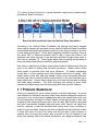
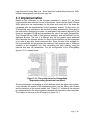
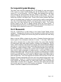
But in order to keep their current lifestyles these demands must be met. Figure
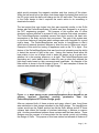
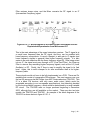
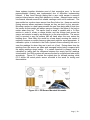
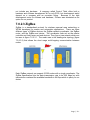
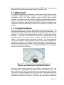
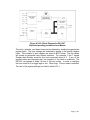
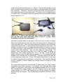
Page | - 1 -
1.0.1 shows a day in the life of a typical American employee as researched by
the National Sleep Foundation.
Figure 1.0.1: Shows the day in the life of a typical American Worker.
Reprinted with permission from the National Sleep Foundation.
According to the National Sleep Foundation the average time spent sleeping
every night is between six and seven hours, while the National Sleep Foundation
recommends that people get between seven and nine hours of sleep to function
at their peak performance. Some other staggering statistics that were found is
that about 25% of American workers tend to take a quick nap while at the
workplace and more than half of the American workforce brings home some of
their work to complete [1]. These figures show how not getting enough sleep at
home can hinder employment productivity and performance.
Now, bear in mind that most alarm clocks cannot solve this dilemma but they do
prove to be useful in dealing with this daily occurrence. Modern alarm clocks
allow people to prioritize their time more efficiently. In today‟s progressive
society time is of the essence and in the business world time is money. With
today‟s alarm clocks they help give people‟s lives a more structured schedule,
this can help them in having a better routine which in turn can help them get a
better night‟s rest. Current alarm clocks have lost their effectiveness in dealing
with these sleep problems. The GuSu prototype will attempt to solve these
issues with a better design that will help people with their dynamic lifestyles.
1.1 Problem Statement
Waking up, especially for some college students, can be troublesome. In a worst
case scenario an individual may have a half dozen alarms scattered throughout a
room set for one or many times, perhaps even with a few outside their room, and
still find themselves shutting all of these alarms off and getting back in bed, only
to wake up later realizing they are late to start the day. Most solutions proposed
and even commercially available have the alarm clock “launch” an object that
must be retrieved, or task the individual with solving some form of problem or
puzzle to quiet the alarm. However this does not defeat the individual who is able
to leave their room to shut off an alarm and still get back in bed, because in
essence this still leaves the person with a snooze or turn off method for the
alarm, and perhaps after a few weeks will become very adept at whatever task
Page | - 2 -
must be performed to silence the alarm, and now have not only spent time
dealing with the alarm, but also gone back to bed, thus resulting in even more
delay to their morning routine.
An alarm clock serves three purposes; waking the user when they wish to be
awoken, getting the user out of bed, and waking them in a "non-harmful" or
disorientating way. These three requirements can be further broken down in the
following way. The alarm clock obviously must be able to keep track of time, and
let the user decide what time they want to wake up. Waking up the user alone is
not enough, the ideal alarm clock ensures that the user also gets up and out of
bed in a timely fashion and stays out of bed (by having no snooze or off button),
in essence preventing both oversleeping and snoozing. Finally, users have
different needs and preferences for being roused from slumber. For example,
some individuals require sudden, often loud or jolting methods, while others wake
better to a slow process, such as subtle music or talk radio followed by lights
coming on, scents of coffee, or an old fashioned alarm tone signifying the time to
get up has passed.
1.2 Solution
Building a clock from the ground up that has no snooze or off button and
removing any direct action on part of the user that can silence the alarm is the
first step in satisfying the three aforementioned design necessities of a better
alarm clock system. But the alarm must turn off somehow, so the clock will
include sensors that tell it whether someone is in the bed or not, and will run off
of the simple logic that if it is time to get up, and someone is in the bed, it will
follow it's programmed routine. This motivates the user by giving them no option
but to get out of bed and stay out of bed. In addition, a battery backup system
serves two purposes; it helps keep the internal clock correct, and ensures the
user cannot silence the alarm by unplugging its power source. The internal clock
itself may be either an atomic clock, set for time-zone by the user, or a binary
clock adjusted by the user.
For meeting a user's "waking preferences" the clock shall have the following
abilities that tie in to the alarm clocks wireless modules and alarm speaker. An
FM tuner, an SD card slot for mp3 storage and mp3 decoder chip, a built in
common tone alarm, Zigbee interfaces with lights and coffee makers, seven day
programmability, and timing/ordering adjustments for what alarm option will occur
(for example if the user would like the FM radio to play through the speaker
fifteen minutes before the wake up time, at which point lights may turn on and the
alarm tone will sound).
To further prevent the user "tricking" the clock into silencing, the alarm settings
can only be changed and tested when a turnkey slot on the bottom of the unit is
turned from the Running mode to a Test/Set mode. This turnkey will be ignored
during the alarm period.
Page | - 3 -
1.3 Research Methodology
The purpose of research methods is to successfully explore information that is
relevant to the design that will be put into practice. There are various methods of
research that are used all the time throughout the academic and professional
disciplines. Some of these methods include use of a library, the internet, and
even life experiences. The purpose of doing research before designing a project
is to measure the idea‟s originality and creativity. There are other factors that
were taken into account which included the significance, contribution, and
technical soundness of the design at hand. Looking at research from another
point of view there are two main aspects that define research; those are
qualitative versus quantitative. When comparing both of these measures of
research the qualitative side can be defined as the measure of the quality of the
project. This means that the qualitative measures will be found in the research
and analysis of the data and physical attributes of the design. On the other side
there is the quantitative approach which includes the research of and analysis of
the numerical data. This side focuses more on the numbers and equations that
will hold the design together.
The main method that was used in designing the GuSu project was the internet
which provided an endless amount of information at the team‟s disposal. The
GuSu project team did countless research and searched the internet for ideas
that suited the team members‟ needs. After we brainstormed and looked at
projects from past UCF Senior Design groups, the team decided on the GuSu
prototype that is explained in detail in this document. Other projects that were
comparable to the GuSu project can be found in section 4.4 of this document.
Once the idea was agreed upon research that used the internet began. This
investigation commenced while we searched for parts and devices that would fit
the brainstormed ideas. The team first searched for each module that was used
in the prototype and compare them to other products of similar likeness. This
method was done for each of the modules that were used in the GuSu design.
After completing this research the most favorable parts were chosen to be used
in its design. Once these parts had been obtained they were put into the design
and implementation phase of the project which will be discussed in sections 1.4
and 1.5 of the document.
1.4 Design Methodology
This section describes the techniques of how the GuSu prototype was designed.
When designing a prototype there are a few dynamics that need to be addressed
before the actual design begins. Some of these include the engineering behind
the design, the marketing which will provide the product to the public and of
course the actual production of the design. First off the research behind the
design must be completed first which was discussed in section 1.4. After doing
so, the plan can be thought about much more. One thing to point out is how the
design‟s ability can conform to professional standards. A number of points that
can be taken into consideration are those of the safety of the design, the
Page | - 4 -
environmental friendliness, and how the designs specifications coincide with any
governmental laws or stipulations. Once these different regulations are taken
into account the design‟s architecture can be thought about.
The GuSu design included various modules that are described throughout this
technical document. These devices were ordered off the internet and put into
practice during the implementation phase of the design. After we received the
parts, the project team studied the various schematics and connections that were
later made. The central part of the design included a PCB (Printed Circuit Board)
that allowed all of these modules to link together. The project team understood
the schematics of the devices and had to create circuitry to allow these devices
to talk to one another.
Team members Josh and Andrew attended a class given at UCF that taught
students to learn how to use the milling machine that created these printed circuit
boards. After we had a better understanding of how this machine creates these
circuit boards the team was able to better recognize how to design the main
board. Following the various schematics behind the devices also allowed the
project team to integrate these into the printed circuit board. Once the devices
successfully communicated with one another, the software design was thought
about. After much research and thought about the design of the GuSu prototype
another methodology was put into practice, this is the implementation phase of
the project which is discussed in the following section.
1.5 Implementation Methodology
This section describes the implementation phase of the design.
The
implementation included the actual building and testing of the prototype. The
purpose of going about the implementation step of designing was ultimately the
deciding factor in which the design had succeeded or failed. As seen in the two
previous sections the research was completed as well as the design
brainstorming and production.
After these steps were completed the GuSu project team then applied this
background information into a real working prototype. The first step in achieving
this methodology had been to assemble the purchased devices in a safe and
secure environment. The purpose of building this in a safe environment ensured
the devices stayed intact and also the builders. Various methods were used
when constructing the devices; such as soldering, wiring, and testing. When we
soldered and wired up each device to one another as well as the printed circuit
board, the project team was careful not to damage the circuitry on the devices.
Simple scratching or high heat can ruin an electrical circuit in an instant.
Page | - 5 -
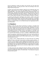
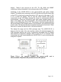
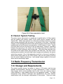
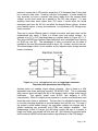
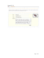
Figure 1.5.1: Overall block diagram of the alarm clock.
Once the devices were connected to one another the testing phase of the
implementation methodology came into place. This phase included all the
directives needed to make sure the hardware was working properly. The project
team had used multi-meters, oscilloscopes, and other electrical testing
equipment to ensure there were no bad connections. As soon as this stage had
been completed and there were no technical errors the software design had
begun. Software design incorporated many different aspects to controlling all of
the devices to perform to the team‟s specifications. This stage of implementation
incorporated a lot of hard work and time to make sure the GuSu design carried
out the actions described in the document.
1.6 Project Management
This section describes the aspects behind what project management meant and
what it did for the designing team. The purpose of project management was a
way to plan, organize, and manage resources at the team‟s disposal to
accomplish the goal that was set for the GuSu project team. The main goal of
the GuSu project team was to successfully implement the design of GuSu and
present it to the fellow Senior Design peers and the UCF faculty. The success of
the design decided whether or not the project team was able to achieve the
various principles that were instilled in the group members throughout their
college career. Some of these principles that were taught throughout the college
program were that of working with others and the ability to apply engineering
practices and ethics. Since the design met the specified requirements the GuSu
Page | - 6 -
project members knew they had accomplished something meaningful and
worthwhile.
To achieve this project management was put into effect. Using project
management ensured that the team had been on schedule and allowed the team
to make sure deadlines were met. The GuSu project team had set up an active
live web folder using Windows Live Mesh which allowed the members to add and
update documents, images, and information. This also allowed each team
member to view each other‟s work and use constructive criticism to make sure
each member was on the right track. Google Documents were also used when
updating documents. The GuSu project team was then using the Google Docs to
update information about billing and specifications. Using these methods proved
to be a way to achieve the organization and management elements of project
management. To achieve the planning aspect of project management a
milestone chart was set up at the beginning of the design. A milestone chart is a
way of depicting key events along a period of time. Most of these events were
deadlines that the GuSu project team had met in order to successfully implement
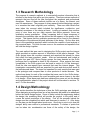
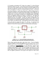
this design. Figure 1.6.1 shows the GuSu milestone chart. Taking into account
all of these factors was key to implement project management in a plan this
complex, otherwise it was extremely difficult to meet all of the goals that were set
beforehand.
Figure 1.6.1: Milestone chart showing project schedule and deadlines.
Page | - 7 -
Back in the beginning of January 2009 when the Senior Design I semester
started the students were told to break into groups of three or four. All four of the
group members have previously been in classes with one another and knew that
this team would work well together. Every Tuesday and Thursday after the
morning class the GuSu team would meet with one another to discuss project
ideas and research methods. After deciding on the GuSu design the team
continued to meet each week, further discussing components that would be used
and how the overall design would function.
The team decided that to break up the 120 page technical design document had
been the best way to tackle this challenge. The document write up was evenly
divided among the four group members and we each choose a module to
research and design. Seen in the following list is a sample of what each member
has worked on.
Andrew: All sections related to Audio output, FM Tuner, Power and
Battery backup, Printed Circuit Boards.
Josh: All sections related to Alarm Clock External Casing, ZigBee,
Appliance Module, Microcontroller, and Clock Module.
Matt: All sections related to LCD display, MP3 decoding, USB reader,
Budgets, Executive and Final Design Summaries.
Philip: All sections related to sensors, User Interface, MP3 decoding,
Software design.
After it was decided which team member would tackle each section, all of the
members worked on the design document on their spare time at home and
school with meetings having continuity from week to week. The team set
deadlines for how many pages would be completed with the average completion
time being 5 pages per week. Keeping with this schedule the team eventually
found that they were ahead of the agenda and had time to spare at the end of the
semester to deal with formatting, appendices, and company emails. The team
met a few times before the deadline to work on formatting and also proof read
the design document. Lastly, the finished documentation needed to be printed
and bound, which was later done at Kinko‟s.
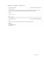
1.7 Similar Projects
There were a few similar projects that were found on the web and in past UCF
Senior Design classes that corresponded to the project this design had
implemented. The team examined all of these projects to get an idea of how to
execute the GuSu system and made it more efficient.
The first project looked into was Lazy@Home [2] designed by a former UCF
Senior Design engineering group. The purpose of this project was a hands free
approach to controlling different aspects of electrical devices within your home.
This group created a base station similar to the GuSu base station that would
Page | - 8 -
control features of the home such as the air conditioning/heating thermostat, the
lighting, vents, and even the wall outlets. The main idea behind this project was
that it allowed the user of the home to control all of these utilities in their home
via web interface so if you left on a vacation you could still control all of your
electrical appliances from the internet. The idea behind this was if the user forgot
to turn off certain lights after you had left the user could easily turn them on or off
from a remote location. Another idea behind this was that when the user was
planning their return home they could easily adjust the thermostat so the home
would be perfectly cooled or heated to their liking. One more interesting feature
that was implemented into the Lazy@Home station was turning on and off
lighting outside of the house. The GuSu project team was very intrigued
because it allowed their users to turn on outside lights at night so it could seem
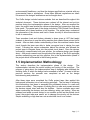
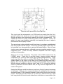
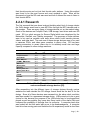
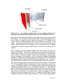
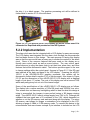
like someone was at home even though no one was there. Seen in figure 1.7.1
are two diagrams taken from Lazy@Home. The image on the left shows the Use
Case diagram of the system and its respective feature components. The image
on the right shows the web interface that this team created to control the
Lazy@Home base station via the internet.
Figure 1.7.1: UML diagram and web interface of the Lazy@Home Senior
Design project. Reprinted pending permission from the Lazy@Home UCF
Senior Design group.
Other projects which were looked at were similar. One was from a UCF senior
design and another from Columbia University. The name of the project at
Columbia University was the OH800 [3], an alarm clock that consisted of a base
and a ball that would shoot out when the alarm was activated. This project
included a solenoid that would push the ball off of the base of the alarm clock
and onto the floor which would disconnect the two magnetic switches. This would
launch a DC motor to turn on inside of the plastic ball and also activate a sound
alarm on the base station. An anti-symmetric disk would rotate within the ball to
move it around the floor. In order to deactivate the alarm the person sleeping
would have to get out of bed and pick up the ball then return it to the base station
Page | - 9 -
which would reconnect the magnetic switches and thus turning off the alarm.
While the ball would sit on the alarm clock base station the battery that would run
the DC motor inside the ball could charge via the AC wall outlet. This was similar
to the GuSu design in that it required the user‟s action to do something to
deactivate the alarm.
The last project that was looked into that was especially similar to the GuSu
design was the PerfectSleepSystem [4] which was also designed by a group in
the UCF engineering program. The purpose of this system was to utilize
electronic sensors attached to a person‟s body to optimize their sleep occasions.
The PerfectSleepSystem contained sensors that would monitor the heart rate,
temperature of the body, and also their movement. The goal of this system was
to use those features to calculate which settings were most favorable for a good
night‟s sleep. The PerfectSleepSystem was similar to Lazy@Home in that it
would control external electronic devices to allow the user to sleep more sound.
Examples of this would be turning off appliances such as the TV or lights. One
feature of the PerfectSleepSystem that was found most interesting was the ability
to detect the amount of light in the room. Having this feature would allow the
base station to turn on its alarm clock to wake the person up at a certain time;
whether it is in the morning, afternoon, or at night. The PerfectSleepSystem was
fascinating as it could detect when to wake the user up when they entered the
light sleep mode based on their movements and heartbeats. An example of the
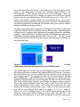
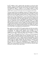
base station is shown in the left image of figure 1.7.2 and examples of where the
sensors were placed are shown in the right image.
Figure 1.7.2: Base station of the PerfectSleepSystem and a diagram of the
sensors
involved.
Reprinted
pending
permission
from
the
PerfectSleepSystem UCF Senior Design group.
After we reviewed both of these projects and many others it was found there
were similarities in their design compared to the GuSu design. The Lazy@Home
system would use the Zigbee protocol as did the GuSu design and all of these
systems had utilized the concept of wireless technology to achieve a common
goal. Another resemblance between these systems was the base station. These
designs used the concept of a base station as the central control unit including
the design of GuSu. The purpose of this base station had allowed all features of
Page | - 10 -
the designs to be easily integrated together. The main difference that was seen
from these designs compared to the GuSu design was the fundamental function
of what each system performed, each system had a different goal to accomplish.
Once these designs were looked into, the GuSu project team got a better feel for
how this design would be implemented and put into effect.
2.0 Case Design
The alarm clock needs to be enclosed in an aesthetically pleasing and durable
case. It will have a single SD card slot and removable back panel for access to
the battery compartment. The three options investigated are an ABS plastic box,
Plexiglas (Lucite) sheets, or a wood case.
2.1 ABS Plastic Enclosures
ABS plastic boxes are readily available from online retailers and local home
hobby stores such as radio shack. They are sturdy, water resistant, and durable.
They are also non conductive. The cases are available in clear to opaque
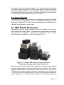
colored boxes and available in a variety of sizes (figure 2.1.1).
Figure 2.1.1: Sample ABS enclosures from Polycase Inc.
Reprinted pending permission from Polycase Inc.
Pre built boxes are designed with holes for switches and buttons while providing
thin walls allowing easier mounting of said buttons and switches. This is also a
drawback for ABS boxes. The enclosure size of the box is also static and the
PCB layout has not been finalized at this point. The design calls for a device size
of 12x4 but this could change based on further PCB designs and additions to
system specifications. The design calls for buttons to be mounted in a circular
Page | - 11 -
fashion which in our research is not available. Many online retailers offer custom
ABS enclosures but the costs are prohibitively expensive.
2.2 Lucite Sheets
With Plexiglas sheets, the box can be constructed to our specifications. It can be
modified easily and adjusted to the final design of the system. A solvent or
adhesive is applied to a finely sanded edge and the solvent is allowed to cure for
12 hours. The edges are then sanded to make a smooth edge. Another option
is using an extruded acrylic adhesive like Weld-on #5. It is applied as glue and
the seams are taped allowing it to dry for 12 hours. While simple to implement,
the aesthetics are certainly compromised with this type of implementation. The
available Lucite products are clear and the user would be able to see the
internals of the system. While some would prefer the look of the clear case, the
group feels this would limit its appeal to a select few.
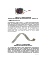
2.3 Wood
Wood sheets are readily available at local home improvement stores in a wide
variety of species. An oak or a maple cabinet grade sheeting with different stains
would certainly provide an aesthetic appeal and are easy materials to use in
construction. Small half inch sections are available for cabinet construction and
can be formed and resized to our specifications. For the aforementioned
reasons, a wood case design was chosen for our product. Simple wood glue and
finishing nails can be used to construct the clock. Holes for buttons can be milled
to any specification and mounting hardware such as standoffs for the PCB can
be drilled directly into the case. The only drawback to the wood design is that it
is flammable. As the system is low power and DC only these concerns are at
most minimal. In order to limit the risk of fire, ventilation shafts and plenty of
open air space can be provided within the enclosure. Adequate heat sinks on
the required components and if necessary cooling fans could also be installed
although this should not be required. The alarm clock system also has a battery
backup in which the battery is internal to the clock. The access door is a simple
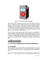
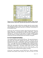
plate attached with four small screws. A sample design is provided in figure
2.1.3.1.
The system also has an external interface for the USB flash module and external
plugs for external sensors. The plugs are modular allowing for the two digital
interfaces for the pressure sensor and the PIR sensor. The plugs will have
different adaptors for both of the sensors to prevent the end user from inserting
the wrong type of adaptor. A single female two pole receptacle will pass through
the case to power all internal devices. A grill was created on one of rear for vent
for the speaker output. Since stereo speakers were not implemented, the two
grill plates were not created. Instead the single speaker was placed directly
below the LCD and is covered with mesh netting.
Page | - 12 -
Figure 2.1.3.1: Sample Clock Case Design
There are five buttons on the top and a hole for the OLED screen in the front.
The LCD screen has mounting holes built directly into the PCB and is screwed
directly to the front face plate. The buttons may require straps through the
terminals to hold them in place. Another option would be to make the top plate a
little thicker ad counter sink holes to hold the buttons and pass the wires through.
In order to make the buttons visually appealing, wood buttons are overlaid and
glued to the off the shelf plastic buttons. A potentiometer is placed on the left
plate to tune the FM tuner to a desired station.
The cost of a wood enclosure is second to ABS in expense for material in the
alarm clock design. Suitable plastic ABS enclosures range in price from $6.50 to
~ $20.00. Wood and Lucite are difficult to estimate based on possible errors that
would require extra materials. Assuming no errors in construction, a single piece
of ½ inch 4‟x4‟‟ cabinet grade oak or maple would be sufficient. The cost for this
piece of wood is around $10.00. The glue and nails would add on an extra
$5.00.
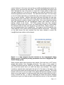
3.0 Microcontroller
3.1 Technical Objectives and Specifications
3.1.1 Goals
The microcontroller is the core component of any embedded system and it is vital
that this device be chosen with care. It must meet all the system requirements
and as well be affordable in regards to the physical device and the development
costs.
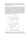
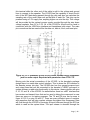
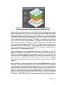
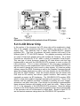
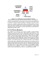
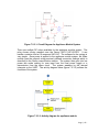
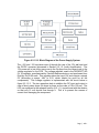
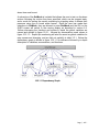
The main microcontroller will interface all of the devices within the alarm clock
(figure 3.1.1.1). This includes any sensors such as passive infrared sensors
Page | - 13 -
(PIR) and/or pressure sensors, the real time clock, the MP3 decoder, the XBee
module, and the . The microcontroller must accomplish the extensive interfacing
and be capable of quick responses for the event driven functions.
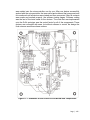
Figure 3.1.1.1: Microcontroller Interface Block Diagram
3.1.1.1 Input/output
For the PIR sensor module, the microcontroller must have a single digital input
pin. Since the PIR sensor module is analog, only a single analog input is required
to monitor the status. Power and ground are also transmitted to the external PIR
sensor. The pressure sensors is also an analog sensor with a single input and a
single output and requires two pins for each sensor. It connects through a
voltage divider network as this provided more precision than measure the actual
resistance through the sensor. The graphical LCD the group has chosen uses
UART as does the XBee module so these two devices will need use two
separate UART pin sets. The MP3 Player and the Real time clock interfaces are
over SPI which is a shared port so the system uses only one set. There is also a
minimum of five buttons for the user interface and each of these uses a single
digital input.
3.1.1.2 Power
To simplify circuit design, devices were sought out which operate in similar
voltage ranges. The common range between devices is 3-5 volts but some
components require more so a voltage regulator will be necessary.
3.1.1.3 Software
Since there are devices communicating wirelessly to separate microcontrollers
the system architectures are similar to aid in design. The ability to use the same
Page | - 14 -
code for both microcontrollers will reduce the amount of code, which decreased
the time it took to develop the software, as well as debugging and maintenance.
Specifically, the selected microcontroller must have an Integrated Development
Environment (IDE) available for it which allows for programming in the C or C++
programming languages. In addition to a common programming language, the
control panel and the microcontroller use the same bit architecture.
3.1.1.4 Physical Package
Both of the microcontrollers are installed on single sided printed circuit boards.
Each of these devices are hand soldered to the boards. In order to make it easier
to mount and solder the microcontroller, all components use a dual in-line
package (DIP).
3.2 Research
After taking into consideration all of the requirements, the range of choices for
the microcontroller were narrowed down to two types. The first choice was from
the Texas Instruments MSP430 microcontroller family. The second choice was
the Atmel AVR line of microcontrollers. The choices were limited to these devices
because of the access to both of the development kits for these, as well as some
experience in developing code for them.
3.2.1 Texas Instruments MSP430
The first and foremost problem with the MSP430 is the availability in packaging.
Texas Instruments provides a wide variety of chips in MSP430 family. The only
problem is that they are all only available in a TSSOP and QFN packaging. The
preferred package type is DIP. The group chose to explore the option of using
the MSP430 with QFN adaptors or sending off PCB and microcontroller for
soldering. The specific device investigated for the project was the
MSP430F2274IRHA. The reason for choosing this device is that it met all of the
requirements excluding dual UART ports and Texas Instruments currently sells a
development kit which is integrated with a ZigBee module using this chip. The
device features a 16-bit RISC CPU, 16-bit registers, and constant generators for
code efficiency. Wake up time from the 5 low power modes is less than 1 µs. It
has two built-in 16 bit timers, a single UART module, 10-bit A/D converter, and
two integrated operational amplifiers. It also supports SPI and I 2C interfaces.
There is an internal low power oscillator which operates at 32 kHz and built in
support for an external RTC. There are 32 I/O pins available. In order to use this
microcontroller the group would have to investigate the use of another LCD.
With 32 I/O pins available, the LCD could easily be supported using TTL logic
instead of the UART interface. Although, controlling a graphical LCD with TTL
logic may add another degree of complexity to the project. The MSP430
operates at 1.8 – 3.6V which is the same voltage as the XBee radios.
Page | - 15 -
3.2.2 Atmel AVR
Atmel manufactures 8 bit microcontrollers under the brand ATmega. This
microcontroller is a high performance, low power consumption, 8 bit RISC
microcontroller [5]. This chip is an ideal candidate for embedded applications
since it is well supported by both its manufacturer and the market. They offer
multiple devices with program memory in the range of 4 - 256 Kb, data memory
from 256 – 2048 Kb, and packages which range from 28 - 100 pins. The
ATmega can operate at as high as 20 MIPS at a clock rate of 20 MHz although
the system is using a real time clock with timers; the chip also has the counters
for use in embedding timing functions. Both internal and external interrupts are
supported which will allow event driven communication over ZigBee and sensor
monitoring. The required voltage supply can be anywhere from 1.8 to 5.5 volts
with a current drawing between 250μA to .1μA which falls in the range of other
modules within the system. This will lower costs by lowering costs in power
system design. ATmega also support boot loaders which will permit remote
upgrading and there are also multiple resources available online for working with
Atmel chips and they are inexpensive. Development Software is also provided
free of charge.
3.2.2.1 Input/output
There are multiple members of the Atmel mega family of microcontrollers that
have at least 20 input/output pins, two serial interfaces and an SPI interface. The
maximum frequencies supported by these chips ranges from 4MHz to 20MHz.
3.2.2.2 Power
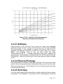
As illustrated in Figure 3.2.2.2.1, the operating voltage for all of the chips is either
1.8V-5.5V or 2.7V-5.5V. The difference in minimum operating voltages varies
depending on the chip selected. The Atmel AVR microcontrollers include a 32
kHz crystal oscillator for use during Power Save mode. This lowers the current
consumption during Power Save mode down to 650nA. Since the appliance
module will not be running continuously, the microcontroller is able to be placed
in power save mode and have wake up events based on button presses or
randomly to check for new information from the alarm clock
Page | - 16 -
Figure 3.2.2.2.1: Supply Current Requirements
Reprinted with permission Atmel [5].
3.2.2.3 Software
Atmel provides a free IDE that can be used for writing and debugging
applications written for all of its chips. The IDE is also used to compile and flash
the microcontroller. It also includes a simulator that can be used to aid in
application development and testing. It allows for program writing in C, Pascal,
BASIC, and assembly. There is also an open source IDE called
Arduino/Sanguino [6] [7]. It enables descriptive coding and simplifies the
programming. The boot loader is compatible with both the ATmega164 and the
ATmega644P. Atmel‟s IDE and Arduino‟s both have extensive support available
online.
3.2.2.4 Physical Package
Both megaAVRs are available as dual inline packages. This makes these chips
good for use in the project because soldering these chips can be done by hand,
rather than being sent out. This will keep the cost of using these particular chips
low and ease prototyping.
3.2.2.5 Summary
All of the Atmel megaAVR microcontrollers meet the specified minimum project
requirements. The availability of each chip as a DIP is advantageous, which will
Page | - 17 -
keep the cost of using them low. Since there are multiple free choices for IDEs,
software development costs are also very low.
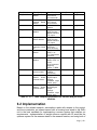
3.3 Implementation
Based on the information in the research presented in section 3.2, an Atmel
microcontroller was selected for use in this project. Atmel site lists three ATmega
AVRs which met our requirements for the clock and nearly all of the chips are
compatible with the specifications for the appliance module. For the clock, the
ATmega644p was used due to the fact that is widely supported by Atmel and by
the open source Arduino boot loader. As anticipated, the memory required for the
clock unit exceeded 25 KB and necessitated the use of the larger Atmega644p.
The ATmega168 has 12KB of flash memory available, and was sufficient, for the
appliance module. The use of a different chip did not require much additional
effort because the software written for Atmel microcontrollers can be recompiled
to be used in any other Atmel microcontroller. Since the size of the software for
the microcontroller did not exceed the maximum flash memory size of 64Kbytes
available in the megaAVR line, then expanding the flash memory using an
external chip was not researched. The pin configuration of the ATmega644p
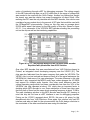
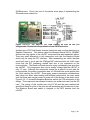
(figure 3.3.1) is shown below.
Figure 3.3.1: Pin configuration for ATmega644p.
Reprinted pending permission from Atmel.
The microcontroller is managing all of the devices within the alarm clock system.
It also handles the control of the appliance module over the XBee radio modem
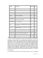
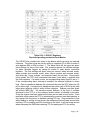
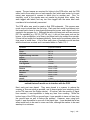
and the detection of the remote sensor unit. Table 3.3.1 outlines all the required
pin assignments for the interconnections between all secondary control modules.
The location of the pins on the ATmega is in figure 3.3.1.
Page | - 18 -
Device
MUX
MUX
ATmega644P
Pin 1 (D0)
Pin 2 (D1)
Device Pin
Pin 5 (MP3 Control)
Pin 2 (FM OUT)
Buzzer
Pin 3 (D2)
Power Buzzer (BZCTRL)
Pin 4 (D3)
Pin 6 (MOSI)
Pin 7 (MISO)
Pin 8 (SCK)
Pin 12 (XTAL2)
Pin 10 (CE/CLKSS)
Pin 13 (SDO/CLKXMIT)
Pin 12 (SDI/CLKRX)
Pin 11 (SCLK/CLKSRL)
Pin 15 (32 KHz/Clockout)
MP3 (Data) - STA013
MP3 (Data) - STA013
MP3 (Data) - STA013
MP3 (Control)
MP3 (Control)
Pin 5 (D4)
Pin 7 (MISO)
Pin 8 (SCK)
Pin 7 (BIT_EN)
Pin 5 (SDI)
Pin 6 (SCKR)
Pin 3 (SDA)
Pin 4 (SCL)
LCD
LCD
Pin 14 (RX0)
Pin 15 (TX0)
Pin 5 (LCDRX)
Pin 3 (LCDXMIT)
XBee
XBee
Pin 16 (RX1)
Pin 17 (TX1)
Pin 2 (DOUT)
Pin 3 (DIN)
Button - up
Button - Down
Button - Left
Button - Right
Button - Select
Pin 35 (D26)
Pin 36 (D27)
Pin 37 (D28)
Pin 38 (D29)
Pin 39 (D30)
Button
Button
Button
Button
Button
PIR
Pin 40 (D31)
Digital Out
Clock - DS1307
Clock - DS1307
Clock - DS1307
Clock - DS1307
Clock - DS1307
Table 3.3.1: Pin Assignments for ATmega644P
3.4 Testing
This included testing of the sleep function, sending data serially, and receiving
data serially. The sleep function was tested by programming the microcontroller
with a simple application that will put it to sleep and wake it up after a given
amount of time. During this test, an amp meter was used to monitor the amount
of current being used by the microcontroller. The results from the amp meter
reflected the appropriate values expected from the calculations in the power
section. The sending of serial data was tested by using the development board
serially linked to a computer (main panel). A simple test application was written
and programmed into the microcontroller that repeatedly sent data serially out of
one of its ports. A terminal on the computer monitored the port and output what it
received over that line. If the data received by the computer matches the data
sent by the microcontroller, then the test passes, otherwise the test fails. The
receiving of serial data was tested by using the development board serially linked
to a computer. The computer sent data serially, and using the Arduino monitor
the data was confirmed. Specific keys were transmitted and confirmed from
Page | - 19 -
alarm clock system and the computer interface module. If the value matches the
data sent by the computer, then the test passes, otherwise the test fails.
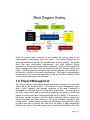
4.0 Alarm Module
4.1 Block Diagram
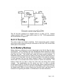
The alarm module consists of an FM tuner, an MP3 decoder, an USB Reader, an
audio amplifier, a speaker, and two buzzers. The microcontroller controls the
power to the FM Tuner and both buzzers, and controls the MP3 Decoder. A
block diagram of the Alarm Module is shown in Figure 4.1.1.
Figure 4.1.1: Block Diagram of the Alarm Module.
4.2. Design Requirements
4.2.1 Audio Output
There are two standard buzzers for the clock that can be used. The
microcontroller is in charge of selecting which output (mp3, standard buzzer
alarm, or the FM radio) will be accessed.
4.2.1.1 Standard Buzzers
Some small amount of research was needed to be done for the common alarm
buzzers. There are several different types, but most of the common ones use a
Page | - 20 -
DC voltage input and output a buzz. Each of them offer different levels of sound
output, measured in decibels (dB). 90 dB should be safe for use of under 8 hrs,
and 85 dB and under would be safe for much longer (it is an exponential
relationship) [8]. As such, the alarm buzzer could easily exceed 85 db without
causing hearing loss as it would only be on for a short time.
A quick search on Digi-key.com showed many different buzzers. A 5mm 2.8 kHz
PCB buzzer with sound output of 85dB minimum was found (part number CEM14R06CT) for $1.24 each. It runs on 40mA. A problem with this model is that it
requires 1.0V to 1.7V DC, which is not in the final design for the clock. Of
course, a step-down could have been used to achieve this voltage, but it was not
necessary, so it was simpler to avoid that. Further searching found a 12mm
(slightly larger) 2.3 kHz PCB buzzer with a sound output of 85 dB minimum and a
maximum current of 30mA. This was the WST-1205S, manufactured by
Soberton Inc. It requires a supply voltage of 4-6V, which is ideal for this clock. It
costs $1.81 each at Digi-Key.com. A second one was found that fit our
specifications nicely, and this was the CPE-503. It runs on 5V, and delivers
95dB output. It cost $3.46 each at Digi-key.com.
The buzzer is activated whenever a voltage is passed through it. Because of
this, the microcontroller passes the 5V whenever the buzzer is needed. A
schematic of the buzzer is shown in Figure 4.2.1.2.1, and the 5VM is controlled
by the microcontroller.
Figure 4.2.1.2.1: Buzzer schematic.
Schematic was made using ExpressSCH.
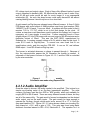
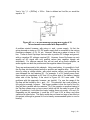
4.2.1.2 Audio Amplifier
Once the output is chosen, the audio needed to be amplified. This is done by a
simple non-inverting setup of an Op-Amp (operational amplifier). The most
common Op-Amps used are the 4558 or 1458 models, which are available for
roughly $0.29 to $0.49 each. There are many different brands of these, but they
are all of the same utility. The gain would of course be dependent on the desired
audio output, and on the audio inputs. The gain cannot be large enough to
saturate the Op-Amp, though, which would occur around 10 or 11 V if the OpAmp was biased at 12V. Figure 4.2.1.2.1 below shows a basic non-inverting OpAmp biased at +-12V, with a gain of 100. This gain was found using basic
electronic formulas learned in EEL 4314, Electronics 2. The equation for it is
Page | - 21 -
Vout = Vin * (1 + (Rf/Rin)) = 10Vin. Gain is defined as Vout/Vin, so would be
equal to 10.
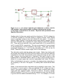
Figure 4.2.1.2.1: A non-inverting Op-Amp with a gain of 10.
This schematic was created with ExpressSCH.
A problem existed, however, with using a + and – power supply. At first, the
group planned on using a +12V DC power supply that is converted to the various
necessary voltages, i.e. 5V, 3V, etc. However, there are no plans to have a -12V
line. There do exist Op-Amps that can take a positive DC voltage and ground,
with no negative DC voltages required [8]. However, these Op-Amps can only
amplify an AC signal with only positive values (any negative signals are
eliminated). For obvious reasons, this will not work as an audio amplifier, as
audio signals use both the positive and the negative sides of the signal.
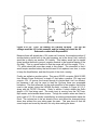
There are workarounds to this obstacle. Using one battery, it is possible to „trick‟
the Op-Amp into being biased as both a positive and negative bias. This can be
done by using a voltage divider, with equal resistor values, and grounding the
zone between the two resistors [8]. For example, if a 12V battery were used,
there would be considered a +6V and -6V on either side of the battery, biasing
either side of the Op-Amp, if the circuit in Figure 4.2.1.2.2 were used. The
problems with this approach, however, are twofold. For one, the range of the
Op-Amp will be limited by the + and – 6V. This shouldn‟t be a real problem in
this group‟s example, however. This bigger problem is that the load of the OpAmp will be in parallel with the resistors. So if the negative or positive biasing of
the Op-Amp draws more or less current (which will be the case for most of the
time of operation), it will offset the loads, making them not exactly +6V and -6V.
Depending on the operations, it could be +5.7V and -6.3V at times, and other
variations at other times. This likely would also not have too large of an effect on
this project, although in general it is not a heavily recommended option to use for
biasing.
Page | - 22 -
Figure 4.2.1.2.2: „Trick‟ for biasing the LM1458 Op-Amp. The top rail
voltage would be +6V in this example, and the bottom rail would be -6V.
Schematic created with ExpressSCH.
Because there will already be a 12V power rail, however, the simplest method (if
another battery would have to be used anyways, as in the above „trick‟ method)
would be to simply use another 12V battery. This battery would just be upside
down (positive terminal to ground, negative terminal to the negative biasing of the
Op-Amp). This is a good method in that the range will be from roughly 11V to 11V, which should be more than ample in this project. The downside, is that it
would require another battery that would need to be replaced over time, in order
to keep the Amplification, and thus the point of the clock, running.
Finally, we settled on another option. This was a DC/DC converter (NKA1212SC
from Murata Power Solutions) a simple IC that takes a positive 12V input and
outputs -12V. Of course, the current through it is limited and it isn‟t too efficient,
but because it will only be used to bias the Op-Amp these are acceptable
limitations. The final schematic for the audio amplifier to the speaker, that will be
used in this project (using the LM1458 Op-Amp), is shown in Figure 4.2.1.2.3,
along with the DC/DC Converter. Refer to section 9 which details the GuSu
alarm‟s +12V line being used. The audio input is coming from the FM Tuner,
Mp3 reader, and standard alarm buzzer. Though the resistor values are listed to
give a gain of 10, Rf is actually controlled by an analog potentiometer inside the
clock. The volume has to be set ahead of time, and cannot be changed during
alarm time without the user taking apart the case. This was done so that the
sound output can be set by the user, but only when setting the alarm.
Page | - 23 -
Figure 4.2.1.2.3: Audio Amplifier Module final schematic.
The Audio In will be controlled by the microcontroller.
Schematic created with ExpressSCH.
After assembling the device and testing it, it was found that the audio was not
amplified quite enough for the internal speaker. So an alternate design
implementation was undertaken. The output from the Op-Amp was split with one
line going to the main speaker and the other line going to an external audio jack
that was taken from an older speaker. This jack was placed on the back side of
the case, and allows the user to plug in external speakers that can amplify the
signal much louder. The original speaker was also included just in case the user
would just unplug the speakers and go back to sleep.
4.2.1.3 Speaker
There are many types of speakers available, and through searching on Digi-Key,
there were many that could fit the needs of this group. Ideally, the speaker would
use a minimum of power/current consumption, output a maximum level of dB, be
as small as possible, be easily integrated into the alarm clock, and have as low of
a cost as possible. Of course, there are no speakers that can deliver all of those
competing ideals, but a decent speaker was found by way of the Panasonic EAS4P15SA. This speaker uses .1W max power, can output up to 92dB, has a
45mm diameter and 18mm height, terminates in solder pads, and costs $4.32
Page | - 24 -
each when purchased without a bulk discount. This speaker was more than
sufficient for the needs of this project.
4.2.2 FM Tuner
An FM tuner was to be integrated with the GuSu alarm clock and needed to be
able to wake the user with any chosen FM radio station. This was to be in
addition to the option for mp3 audio from the on board SD card slot and standard
alarm beeping. It was intended for the device to use a minimum number of parts,
and the radio needed to be able to be tuned by the user to any local station that
has strong enough of reception to be easily picked up. In this case, that would
be all FM stations that are broadcast from the Orlando area. The tuning needed
to be relatively easy for the user to do; with a user interface on the outside of the
alarm clock housing unit allowing access to change the stations. This could be
done with an analog knob or two buttons, depending on the method of reception.
The radio needed to be able to tune at every 200 kHz frequency interval from
87.5 MHz to 107.9 MHz, which is the frequency range for broadcast FM radio in
America. It was also important that the radio is properly selective.
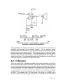
4.2.2.1 Research
The process of integrating an FM Tuner into the clock began with identifying the
various alternatives that are available. Through researching online, it became
apparent that there were two main ways to do this. Several circuits could be built
from scratch and connected, or a partially or completely prebuilt receiver could
be purchased.
There are many different circuits that could be built from scratch, from a
(somewhat) simple single transistor receiver to more complex super heterodyne
receiver circuits. The most common radio receiver today (and it has been for
well over 50 years) is the super heterodyne receiver (short for supersonic
heterodyne receiver) [9]. A block diagram of the important elements of this
receiver is shown below in figure 4.2.2.1.1.
The RF input, received from an antenna, is fed through a filter (the Preselector
Filter) to severely limit the frequencies passing through to a narrow band
including the frequency that is wanted. The Limiter acts similarly to a surge
protector; if a seriously high powered signal were to come through the RF input,
this limiter would protect the LNA (Low Noise Amplifier). The Switchable
Attenuator is able to, as needed, slightly reduce the strength of the signal if it is
strong enough to saturate the LNA. Next, the LNA amplifies the signal, though it
is important that it is not damaged by too much power hitting it. Any damage
done is permanent. The amplifier‟s purpose is to amplify the main signal to a
point where it is further distinguishable from the background noise). The Image
Page | - 25 -
Filter reduces image noise, and the Mixer converts the RF signal to an IF
(Intermediate Frequency) signal.
Figure 4.2.2.1.1: Block diagram of a common super heterodyne receiver.
Reprinted with permission from Microwaves101.
This is the main advantage of the super heterodyne receiver. The IF signal is at
a much lower frequency than the RF signal, and thus, can be modified with
lower-frequency components. It is much „cheaper‟ to add gain to IF signals (and
lower frequency signals in general) than higher frequency signals. It is also
easier to be more selective with the lower frequency signal [9]. After being mixed
into an IF, the signal must pass through a LPF (Low Pass Filter), the Clean-up
Filter to remove any remaining higher frequency signals, such as the LO (Local
Oscillator) or RF. Finally, the IF Amp is used to amplify the signal to its final
level. Again, this is much cheaper to do after modulation than at its higherfrequency state.
These circuits would not have to be fully implemented on a PCB. There are ICs
available that consist of regenerative FM receivers. The most common one over
the last 20 years may be the Phillips (now NXP Semiconductors) TDA7000. This
IC is a basic FM receiver, with only mono audio output (which would be
acceptable according to our one-speaker specifications), and selectivity decided
by the local oscillation frequency, which would be determined by a small variable
RC circuit. The TDA7000 were no longer produced beginning in December
2003, although they are still available on the market. There are also two later
models, the TDA7010 and TDA7021. An example of the block diagrams of the
TDA7010 is shown below in figure 4.2.2.1.4.
Page | - 26 -
Figure 4.2.2.1.4: Block diagram of the TDA7010.
Reprinted with permission from Digi-Key.
This circuit could be implemented on a PCB board more easily than the “do-ityourself” method, but would eat a lot of space and use a lot of components
(though the space and components required are minimal comparatively). The
variable RC circuit for tuning could also present some problems. One of the
goals is for easy user frequency selectivity, and requiring the user to adjust a
potentiometer would qualify as such.
The second main option available would have been to purchase a prefabricated
chip that includes the FM receiver. These are generally digital circuits that can
be controlled by a microcontroller to receive the desired station. Most of these
circuits require external elements, although some are complete receivers in one
integrated circuit. There are many different companies that offer varying
solutions to this problem.
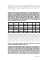
Sanyo is one of such companies. They have a line of FM receivers from the
LV24000 series. These are all one-chip tuners, requiring minimal external
components [10]. Some of these chips even include internal antennas. These
tuners also have the ability to include RDS (Radio Data System). The RDS
system allows for the output of the name of the station/song and band that is
playing. One nice thing about this line of chips is their versatility; they have many
different features available on different chips. Table 4.2.2.1.4 shows the different
tuners in production and their feature sets, as they would be applicable to the
needs of this project.
Having the AM tuner would have been a nice bonus, though it was not necessary
to this project. While any true commercial release of a project like this one would
doubtlessly need it, FM is generally listened to much more often by most younger
people. Especially since the function of our alarm is to wake the user up; a loud
rock song would do the trick much faster than a talk show or news station (the
Page | - 27 -
kind of shows that are found more frequently on the AM band). The RDS
decoder would be handy, though also most definitely not a necessity. The user
knowing the name of the song that is playing is of less importance than the actual
waking up. RDS functions would have more necessity in systems where the
main function is to listen to and enjoy the music/programming. Most of the
LV24000 lines of chips are 3-wire controlled, but the couple that are I2C is noted.
The headphone amp is not truly needed either, because another audio amplifier
is used elsewhere in the GuSu system.
Model #
LV24003
LV24010
LV24100
LV24230
LV24233
+AM Tuning
+RDS
2
I C Controlled
+Headphone Amp
X
X
X
X
X
X
Table 4.2.2.1.4: Sanyo FM tuner one-chip solutions [10].
Sanyo was contacted via email, and they were very helpful. They provided help
with locating the part in the event that the group had decided to go with it, and
they also gave important documents such as the datasheet, access to their
LV24230 „Easy Radio‟ schematics and information, and offered to help however
they could during the process.
Another company worth looking into was Silicon Labs. They also have many FM
tuners on the market, most notably their line of Si470X ICs. These receivers do
require external components, although the amount is minimal. Each model, like
the Sanyo receivers, has different feature sets. The Si4702 and Si4703 models
offer full FM receiving, with the Si4703 model including RDS decoding. The
Si4704 and Si4705 models improve on the previous versions with Bluetooth
capability, and will accept transmissions in that format. The 4705 chip also
includes the RDS decoding. The Si4708 and Si4709 chips improve on those by
decreasing the size to an amazing 6.25 mm 2, again with the Si4709 including the
RDS decoding.
An example of the Si4704/05 models (with necessary
components included) is shown below in figure 4.2.2.1.5.
These models all seem to be difficult to order just one of; most of the authorized
retailers require minimum purchases of over 2500 parts. Digi-Key had none
available of any of the above models. Avnet Memec had only the Si4709 and the
Si4703 part readily available, for $13.75 a piece. Nu Horizons had none of the
above, and Mouser Electronics had the Si4704 for $9.21.
Page | - 28 -
Figure 4.2.2.1.5: A block diagram of the Si4704/05 FM tuner. Notice the few
needed external components. Reprinted with permission from Silicon Labs.
Silicon Labs was similarly helpful when contacted about the group‟s project.
They responded promptly to emails, and their local sales liaison quickly replied
with the datasheets, latest device errata, tips for PCB layout, and information on
the embedded antenna.
A third option that could have been possibly implemented would have been from
Silicon Labs as well. This project did not support a USB reader. If that had
changed, Silicon Labs does manufacture an FM Tuner that is embedded into a
USD card [11]. This looks to be used mainly for computer operating systems
using their software to decode and play the music; however, it is reasonable to
assume that it could be controlled with the microcontroller in this project.
4.2.2.2 Implementation
It was originally decided to use the Si4704 FM tuner. This was picked because it
was cheap, small, and easily integrated and controlled. One was found on
www.mouser.com for $9.21. It was ordered, it came in, and the group was very
surprised as to how small it was (although it was exactly as advertised, 3mm X
3mm). It also came with no pins, and apparently needs a special machine to
„press‟ it onto a PCB. At this point, the Si4704 FM tuner was no longer a viable
candidate for implementation. The Sanyo LV24000 series of FM Tuners was
reinvestigated, and the same size/mounting issues remain with them. It was
decided that the use of these specialty one-chip tuner chips should be left to the
companies that have the abilities and the facilities to use them.
At that point, it was decided to use the TDA7000 chip. While all mainstream
electronics stores (Mouser, Avnet, Digi-Key, etc.) were out of stock on it (if the
Page | - 29 -
part was even listed), a few of them were found on E-Bay. 2 were purchased for
$21.25 from littlediode_usa. Using resources found online, including the
datasheet for it and a couple of helpful websites, the schematic in Figure
4.2.2.2.1 was created [12] [13].
As can be seen 4.2.2.2.1, there are many external components to be integrated,
including 16 capacitors. The tuning is determined by three things: the input
voltage, the variable coil (L1), and the potentiometer. The easiest way to set up
the tuning for the user is to take the following steps [12]. First, for FM reception,
the input voltage should be around 4.5V to 5V (5V will be used, as it is a common
voltage level through the alarm clock). Next, the variable coil should be used to
tune to the upper (or lower) frequency. In the case of FM reception, that would
be 108 MHz (or 88 MHz). Finally, the potentiometer can be used to fine-tune the
frequency between the specified ranges. This potentiometer also does not need
to be attached directly to the PCB; it could be attached to the casing of the alarm
clock with wires going to the PCB to be soldered on. This would allow the user to
change radio stations without opening the casing.
Figure 4.2.2.2.1: Final design of the TDA7000 FM Tuner implementation.
Schematic created using ExpressSCH.
The antenna A1 can be built a couple of ways. Ideally, the clock will not have
any exterior antennas. An interior antenna can be used that is at least 10 cm
long, and to be on the safe side, a longer one will likely be used. Another
Page | - 30 -
important criterion would be a lack of interference, and one other component in
the clock could cause some serious interference: the Zigbee device. Because of
that, the FM tuner and the Zigbee device should be placed on opposite ends of
the PCB, and the antenna for the tuner should stay on that end of the clock.
The audio output level of the TDA7000 is about 75mA. This is amplified by the
audio amplifier, as needed to produce an optimal loud noise. The power signal
is supplied by the multiplexer when the FM tuner is selected by the
microcontroller.
4.2.2.3 Testing
The FM receiver was tested on its own breadboard first. It was powered, and
connected to an amplified speaker. While there were initially problems with the
variable inductor, the group got the device working and were able to select from
the major radio stations in the area. The selectivity was extreme, however,
although it was somewhat helped by including a 50k resistor in series and a 100k
resistor in parallel with the 100k potentiometer. This was because all the stations
were located in the upper 50k of the potentiometer range.
4.2.3 MP3 Decoder
To accommodate user comfort and preference, the Get Up Stay Up (GuSu)
Alarm System has the ability to read and play MP3 files as audio output in
addition to the other alarm audio/action options. This allows the user to choose
any of the music or sound file they own or can create using one of the many
available free and open source audio recording software as the alarm's wake up
sound, greatly widening the alarm's range of available options for waking it's
user. The storage of MP3 files is handled by the on board USB Flash Drive slot
discussed in its own section. In order to make use of the data stored on the USB
Flash Drive hardware and/or software is required in order to decode the files and
process them. ID3 tags can also be handled to display the song name and artist
on the GuSu's LCD screen.
4.2.3.1 Research
Due to the GuSu's architecture a software solution to handling MP3 audio playing
required many hours of coding and pins that were dedicated to reading from the
SD slot and passing along audio to the GuSu's speaker output, greatly
decreasing the number of available pins for other uses. A hardware solution
involving an MP3 decoder chip was a much more convenient and stable solution
considering pins would only be required to send control signals to the MP3
decoder chip and relieve the engineers of the burden of software creation and
testing. The team put a lot of effort into researching what MP3 Decoder to use
with the GuSu prototype and it proved to be a difficult challenge deciding which
decoder would work best with the design at hand. One of the main sources that
were used in looking for MP3 decoders was Sparkfun electronics, this company
Page | - 31 -
seemed to hold a large array of different types of MP3 decoders. Some other
companies found on the web that carried MP3 decoders were PJRC electronics
and STMicroelectronics. The following contains information on the various MP3
decoders that were considered along with their specifications and why they were
or were not chosen.
Possible solutions range from lone decoder chips, to integrate-ready boards, all
the way up to fully assembled boards which only require a storage device be
connected. While the third option was convenient, the prices range over a $100
and would have been harder to interface with from the GuSu system without
either modifying the board received or having separate controls. In addition the
excess parts and components jeopardized the design plans for keeping the
GuSu as small as possible. The second option did not have this problem, and
parts were usually priced under $50. Below (table 4.2.3.1.1) is a table comparing
some of the available MP3 mini circuit boards.
Item No./Name
On-board
Chip
VLSI VS1002
Interface
Output/Input
Dimensions
Price
Supplier
SPI
45 x 55 mm
$ 23.90
[15]
SD card
N/A
80.00 €
[14]
USB
Audio Out
N/A
80.00 €
[14]
SD Card
80.00 €
[14]
57 x 45 mm
$ 41.94
[20]
BOB=07832
VLSI VS1002
Microphone
Audio Out
Microphone
Audio Out
Microphone
Audio Out
N/A
MOD-MP3
VLSI
VS1003B-L
VLSI
VS1000B-L
VLSI
VS1053B-L
VLSI VS1002
Microphone
Audio Out
Audio Out
57 x 45 mm
$ 40.95
[21]
MINIMP3
VS1003B-L SD
Card Mini Player
VS1000B-L Tiny
Player
VS1053B-L
UEXT
SD/MMC
UEXT
SD/MMC
Table 4.2.3.1.1: Comparison of MP3 mini circuit boards
Some of these mini boards did include SD capability built in, however most used
battery power, already had buttons soldered to the control lines, and included
parts or capabilities not needed for the GuSu system. Another complication was
controlling audio output for the system when the output lines were already
connected to audio jacks and microphone lines for encoding. Extra hardware
presented complications for running on battery backup during alarm time, and
having unused hardware and controls sitting idle also interfered with other
signals to and from the main micro-controller. Therefore, with respect to routing
of audio, control, power consumption, and overall design size, the optimum
solution was to integrate a lone MP3 decoder chip.
One of the first decoders looked at was the VS1053b [20]. This chip was very
interesting in that it had the ability to decode multiple audio file formats and not
just MP3s. Some of the file formats the VS1053b was capable of decoding were
Ogg, MP3, ACC, WMA, and MIDI. The team thought this chip was a good fit for
the GuSu design because of its potential to decipher the high quality Ogg sound
format. Although this was a great attribute to this chip, the chip did require
additional software plug-ins to handle these file formats. Some specifications for
the VS1053b chip were that it was controlled via a serial input bus and had the
Page | - 32 -
option of interfacing through uART for debugging purposes. The voltage supply
to this MP3 decoder chip was ran at 3.6V which was in the range of voltage that
was needed to be used with the GuSu Design. Another key feature that caught
the team‟s eye was the relative low power consumption at about 50mA. After
realizing that SPI was the only interface with this MP3 decoder, this solution was
considered a poor product due to the amount of SPI pins that would be used with
the ATMega644P microcontroller. Pricing on this chip was on average about
$19.95 which wasn‟t that pricey for the high quality of this chip. Shown in figure
4.2.3.1.1 is a schematic of the VS1053b MP3 decoder showing the processing
unit on the chip as well as the interfacing capabilities.
Figure 4.2.3.1.1: The package design of the VS1053b audio decoder.
Reprinted with permission from VLSI Solution.
One other MP3 decoder that was manufactured from VLSI Solutions based in
Finland, an integrated circuit developing company was the VS1001 [21]. This
chip was also fabricated from the same company that made the VS1053b. The
VS1001 chip is not as involved and does not have all of the extra features as the
VS1053b but it had some of its own advantages. The main difference in this chip
was that it only supported the MPEG audio layer codec whereas the VS1053b
had support for multiple audio formats. One other small difference was the
voltage operating range which had been considerably less than the 3.6V of the
VS1053b; this chip operated at about 3.3V which was an important factor in
deciding which MP3 decoder to use. Some similarities of these two chips were
that they both of them had the same clock operating frequency at about 13 MHz.
The main interfacing solution to this MP3 decoder was through SPI, bearing in
mind this chip did not have a uART interface to use for debugging purposes.
Pricing on the VS1001 averaged about $21.00; this was a bit pricey for this
discontinued chip from VLSI Solutions. Once again, this solution only had SPI
interface and was not ideal for the microcontroller the GuSu design used due to
the constraints of the other modules that were using this interface.
Page | - 33 -
Lastly, the team had found an ideal candidate MP3 decoder that worked easily
with the ATMega644P microcontroller and the SD Card Reader. This chip was
called the STA013 MP3 decoder developed by STMicroelectronics. The main
feature of the STA013 decoder was that it could handle just deciphering of
MPEG layer 3 formats, specifically MP3s. This differed from the other decoders
that were researched in that the STA013 only dealt with one type of file format
which made it idyllic for handling just MP3s, which are the most popular form of
sound format on the market today. When decoding these formats the STA013
had a special ability to output information in stereo, dual channel, or mono sound
types. The STA013 was run off of 3.3V and helped with the GuSu design
because this was low voltage for a decoder. Surprisingly enough the STA013
had very low power consumption at 85mW and also a lower clock frequency than
the other MP3 decoders that were researched running at 10 MHz. A key feature
that caught the eyes of the team members had been the I2C interface capability.
Having essentially used all of the uART and SPI interface pins on the
microcontroller there were a few digital pins left for I2C interface. Pricing on the
STA013 was set at around an average of $20.00 which lined up with the other
decoders looked at. Since all of the decoders were about the same price and due
to the fact that the team needed a device with I2C operation the STA013 was the
right decoder for the price and features.
The STA013 has two modes of operation; it can work in either Multimedia mode
or Broadcast mode. In the Multimedia operation mode the STA013 decoded the
incoming MP3 data streams and output them to the speaker with much ease.
This type of operating was controlled by buffer management that was embedded
on the software within the decoder. While operating in the other mode, the
STA013 received a data stream but had to check that the bit rate of the incoming
MP3 data matched the actual bit rate of the stream that was being decoded. One
important fact about the STA013 I2C data bus was that it would always act as a
slave device instead of a master when connected to the microcontroller and
speakers. Shown in figure 4.2.3.1.2 are the absolute maximum ratings of the
STA013 decoder.
Figure 4.2.3.1.2: The absolute maximum ratings of the STA013 MP3
Decoder. Reprinted pending permission from STMicroelectronics.
Having done the research on these different decoders it seemed like the STA013
was the best fit for the implementation of the GuSu system. The VS1053b
seemed like a great choice but the team only cared about the MP3 formatting of
audio files. Dealing with different formats of files had proved to complicate the
Page | - 34 -
design much more than it already was. Having the data interface as I2C also
helped the team choose this chip over the others. Thus, this proved to be the
pick for the GuSu design. The implementation of the STA013 decoder chip will
be discussed in further detail in section 4.2.3.2 of the document.
4.2.3.2 Implementation
After doing much testing with the STA013 MP3 decoder it was decided to drop
this component from the GuSu prototype. Reasons for abandoning this decoder
are given in the testing section of the MP3 decoder. The team went back and
looked into the researched MP3 decoders to look for a different one and the
VS1003 from VLSI Solution was chosen to be implemented on the GuSu system.
The VS1003 is a single-chip MP3/WMA/MIDI/WAV audio decoder. On this chip is
a high performance and low power DSP processor. It has the capability of
decoding MPEG 1, 2, and layer 3 audio files in CBR, VBR, or ABR format. To
operate the VS1003 the analog and digital positive voltage supply does not
exceed 3.3V and a 12 or 13 MHz clock is used. Power consumption of the
VS1003 is considerably small at only 50mA. A key feature that this decoder uses
to ensure good audio output is the high-quality stereo digital to analog converter
that does not allow any phase errors between channels. If no decodable data is
found, the VS1003 will enter idle mode. This audio decoder has a uART interface
that allows for debugging purposes when implementing software to control this
device. The VS1003 is used in conjunction with the VMusic 2 device that is
discussed in further detail in the SD/USB section of the document. Shown in
figure 4.2.3.2.1 is the flow of data through the VS1003 audio decoder.
Figure 4.2.3.2.1: Data flow of the VS1003 Audio Decoder.
Reprinted with permission from VLSI Solution.
Since the VS1003 decoder is embedded into the VMusic 2 which is discussed in
the SD Card/USB Drive section there is not much that the team had to implement
on this device. Figure 4.2.3.2.2 shows the schematic of the VS1003 audio
decoder connected to a headphone jack which is used for audio output. Once
data is decoded through this device there is a left and right output connected to
a phonejack stereo component. A 3.5mm audio cable will be used to connect to
Page | - 35 -
this terminal while the other end of the cable is split to the voltage and ground
lines to connect to the speaker. The VS1003 has the capability to check the bit
rate of the MP3 data being passed through the chip and also can calculate the
sampling rate of the audio data such as the MHz of each file. This chip can be
powered using a 3.3V supply line, anything higher can ruin the chip. This voltage
will be provided by the system‟s power supply provided through the step down
voltage regulator from 5V to 3.3V. All of the VS1003‟s 48 pins will be used in
connection with the USB Drive interface and headphone jack output. The main
pin connections that are used will be the data out, data in, clock, and reset pins.
Figure 4.2.3.2.2: Schematic of the VS1003 Audio Decoder with a headphone
jack for audio output. Reprinted with permission from FTDI LTD.
Moving onto the actual connections of the VS1003, in the decoder‟s package
design there is a serial data control interface. This is where the SPI interface to
the decoder comes into play. The VS1003 also has four general purpose input
and output lines that can be connected to the decoder‟s VSDSP processor to
update software or add extra functionality to this device, these coincide with pins
9, 10, 33, and 34 of the VS1003. As stated before there is a uART interface that
has receive and transmit lines that can be used to debug the component in case
there are errors or for testing purposes. The TX and RX pins can be seen in
figure 4.2.3.2.2 on pins 26 and 27. There are many different types of resistors
and capacitors that will help regulate voltages throughout this component. Data
will flow through the VS1003 by receiving its input bitstream through the SPI bus
which is used as the system slave. The input stream is decoded through the
Page | - 36 -
various stages of the package and then is sent to a digital to analog converter
that is already embedded onto the chip.
Dealing with the software to control this audio decoder will be fairly simple.
Software code needed to be implemented on the ATMega644P microcontroller;
the first bit of code would be used to read in data from the USB Flash drive which
is connected to the VMusic 2 module. This would allow the microcontroller to
control the module that contained the VS1003 and the USB flash drive reader.
There would only be one function that needed to be on the ATMega644P which
is the read function. More on the implementation about this chip and the module
it is embedded onto is talked about in the next section, Testing.
4.2.3.3 Testing
There were many reasons that the team decided to drop the STA013 MP3
decoder. When the device came in the team immediately went to work testing its
functionality on a breadboard. It was soon discovered that this device required
much more implementation than was planned for. There was much trouble in
finding the 14.7456 MHz crystal that it needed to operate and there were a large
amount of resistors and capacitors that would have had to been used to use
them on the printed circuit board. There was success in powering the STA013 by
connecting it to a 2.9V voltage source and ground. There was a sample program
provided in the Arduino libraries, but it was written in C code. All of the software
libraries for the GuSu were being written in C++. After seeing the software to
control this device it came to our attention that this component would be
extremely complex to write software for. On top of these problems there were a
lot of misfortunes when dealing with the SD Card reader. Finally, after time was
running short with the deadline of the project approaching the decision was made
to drop this component. The team went back and looked at the research that was
done before and we realized that an audio decoder from VLSI Solution were
ultimately the best choice. Modules were looked at that included both the SD
Card/USB Drive interface and an audio decoder from VLSI. VMusic 2 included
the VS1003 decoder which has the ability to decode different audio formats than
just MP3s like the STA013 could do. Testing with this device was found to be
much easier because the VS1003 was embedded on a printed circuit board
inside the VMuisc 2 module. Powering the device included a 5V voltage source
provided by the microcontroller. A simple script was written in C++ to test the
functionality of the device. We were successful to get audio output from the
VMusic 2. More information about the VMusic 2 is discussed in the
implementation section of the SD Card/USB Flash drive reader.
4.2.4 Sim Card/USB Drive Reader
The purpose of the SD Card Reader allowed the user of the GuSu prototype to
store their favorite songs and music on a widely available Secure Disk for
playback through the GuSu‟s sound output. The reasoning behind this was so
that besides the FM Tuner the user could also have a backup way of listening to
Page | - 37 -
their favorite music and not just their favorite radio stations. Using this method
was found to be the most secure and most updated to date. More will be
discussed on how the SD card was used and how it allowed the user to listen to
their favorite MP3s.
4.2.4.1 Research
The first research that was done involved deciding what kind of storage device
the GuSu design would use to pass MP3 files through the MP3 decoder and to
the speaker. There are many types of storage devices out on the market today.
Some of the devices are Compact Flash, USB storage, hard drives and even SD
cards. SD is a short acronym for Secure Digital which was developed by the
Matsushita, SanDisk, and Toshiba companies. The purposes of these devices
were to be used as portable solid state drives which could transfer pictures,
videos, and other data. The main use of these storage devices were to be used
in cameras, PDAs, and video game consoles to name a few. SD has been
gaining momentum in recent years due to its relatively small size and large
capacity compared to other storage mediums.
Card
Compact Flash I
Compact Flash II
Smart Media
MMC, MMCplus
RS-MMC, MMCmobile
MMCmicro
Memory Stick
Standard
Memory Stick Duo
Memory Stick Micro
SD
miniSD
microSD
xD
USB
Width,
mm
43.0
43.0
37.0
Length,
mm
36.0
36.0
45.0
Thickness, mm
Volume, mm^2
Mass, g
3.3
5.0
0.76
5108
7740
1265
3.3
24.0
24.0
14.0
21.5
32.0
16.0
12.0
50.0
1.4
1.4
1.1
2.8
1075
538
185
3010
1.3
1.3
20.0
12.5
24.0
20.0
15.0
25.0
Varies
31.0
15.0
32.0
21.5
11.0
20.0
Varies
1.6
1.2
2.1
1.4
1.0
1.78
Varies
992
225
1613
602
165
890
Varies
2.0
2.0
2.0
1.0
0.27
2.8
Varies
2.0
4.0
Table 4.2.4.1.1: The relative sizes and masses of
various multimedia storage devices [22].
After researching into the different types of storage devices through various
websites the team decided the SD storage format would be the best fit for the
design. Since all of these devices were encased into the alarm clock a solution
was then needed for a permanent storage device. USB proved not to be a good
choice for this because the purpose of the USB sticks was to be plugged and
played as well as portable; they were also flimsy inside of the alarm clock and
increased the possibility of dislodge from its connector. A computer hard drive
was looked into but this would also prove to be disadvantageous. A computer
hard drive has moving parts and therefore the life expectancy would be less than
Page | - 38 -
that of the other solid state drives. A hard drive would also draw way too much
power for the alarm clock to handle and interfacing these devices to the
microcontroller or MP3 decoder proved to be very challenging. After we
eliminated these devices from our design, the team found that the SD storage
medium was the most advantageous for the GuSu alarm clock. Table 4.2.4.1.1
shows some different storage mediums and their relative size to one another.
The actually storage capacity also varies from one to the other. Researching into
the Secure Digital format showed that this allowed for the most capacity variation
between the different storage mediums.
The team‟s first choice when looking into SD storage formats was a special type
of SD Card Reader that would interface with the MP3 decoder. Researching into
GHIElectronics, a company which specialized in storage mediums for embedded
systems; it was found that they produced an SD Card Reader that used various
interfacing connections which included uART, SPI, and I2C. This also proved
useful in connecting to the MP3 decoder because this component contained all of
the interfacing types.
Figure 4.2.4.1.1: The diagram of the uALFAT and how it interfaces to other
components. Reprinted with permission from GHI Electronics.
This device called the uALFAT [24] provided support for the FAT16 and FAT32
file systems which were excellent when dealing with the MP3 format. This device
also allowed the user up to four simultaneous file accesses, had a fast start up
and reconnect speed. The average file read from this device was on average
about 60KByes/sec. With GHIElectronic‟s new firmware the uALFAT was also
capable of interfacing with the new and improved SD cards like the SDHC cards.
This Secure Digital High Capacity card allowed for greater storage capacity.
Some other key specifications were that it had a Real Clock Time and a low
power consumption of about 12mA. This would prove useful with all of the
devices that the alarm clock had been using. Lastly, all of the input and output
pins had a 5 volt tolerance which was in our range of 3.3V to 5V. Shown in
Figure 4.2.4.1.2 is a sample image of the uALFAT device along with the pin
schematic showing the different interfaces using uART, SPI, and I2C. The
pricing was fairly expensive for this small component at $44.95 a piece from
Page | - 39 -
GHIElectronics. Due to the cost of this device more ways of implementing the
SD reader were looked into.
Figure 4.2.4.1.2: The uALFAT SD Card Reader as well as the pin
assignments. Reprinted with permission from GHI Electronics.
Another type of SD Card Reader that was looked into was one that was found on
Sparkfun electronics. This device called the Breakout Board [25] for SD/MMC
devices was very similar to the uALFAT component that was researched above.
There are small differences in this component such that the Breakout Board
would only be using the SPI interface. After researching into which interface
would suit best to work with the ATMega644P microcontroller the GuSu team
found that the SPI interfacing worked best due to pin constraints on the
microcontroller. The Breakout Board was also using considerably less pins than
the uALFAT. This component also used a smaller voltage than the uALFAT at
only 3.3 volts. Although this component seems like a great fit to work with the
microcontroller, the power consumption was a 0.5A which was much greater than
the 12mA used by the uALFAT. Once again, power consumption considerations
were taken into effect when dealing with different components, the team made
sure that there was enough current to power all of the devices in the alarm clock.
Figure 4.2.4.1.3 shows the Breakout Board as well as the PCB schematic of this
design. This component also allowed for data to be written and read from the SD
card. The pricing of this module was only $17.95 and the team realized this
would be a better buy due to the price as well as dealing with the amount of pins.
The Breakout Board was easier to integrate to the MP3 decoder than the
uALFAT.
Page | - 40 -
Figure 4.2.4.1.3: The Breakout Board SD Card Reader and its dimensions.
Reprinted with permission from Sparkfun Electronics.
One more type of reader that was researched into was the USB SD Card Reader
[26] from Sparkfun Electronics. This device seemed like a great choice for the
GuSu prototype because it had support for all of the different types of SD formats
such as SD, microSD, MMC, and compact flash. After realizing that the GuSu
prototype needed some type of USB interface with the MP3 decoder the team
thought that this proved to be a more challenging task that required extra work.
Finding a USB interface that would interface easily with the STA013 MP3
decoder proved to add a lot of extra programming work on top of the large
amount of programming already needed to be done. The team thought of
another easy way to get around this by directly interfacing the USB SD Reader to
the ATMega644P. Doing it this way proved useful in that the microcontroller
could control the data being read from the SD card and would pass it to the MP3
decoder and then out the speaker. The team finally decided that this was the
worst choice for the SD Card Reader because the USB interface to the
microcontroller needed a way to be powered and this was adding to much
implementation just for this one module of the GuSu alarm clock.
4.2.4.2 Implementation
After doing much testing with the SD Card reader it was decided to drop this
component from the GuSu prototype. Reasons for abandoning this media reader
are given in the testing section of the SD Card/USB Drive reader. The team went
back and looked into the researched ways of reading media from a storage
device. Although most of the research was done on SD Card readers, it was
strongly felt that this device required an excessive amount of implementation and
with time running short a more simple method of reading media was looked into.
The team came across the VMusic 2 media module and it was decided to use
this.
Firstly, what is the VMuisc 2 media module? The VMusic 2 module from FTDI
Limited is an all inclusive media handler that has a USB host controller as well as
the VS1003 audio decoder. Some of the specs behind this device are as follows.
It contains the VNC1L-1A USB host controller which allows for the insertion of a
USB flash drive that can store audio media. This controller is paired in line with
the VS1003 audio decoder which was described in the previous section [27]. The
Page | - 41 -
type of USB socket to connect with the flash media drive is type „A‟. For audio
output, the VMusic 2 has a stereo 3.5mm headphone jack that a cable can be
connected to, this is where the speaker will be connected to. Seen in figure
4.2.4.2.1 is the schematic of the USB host controller. There are two different
types of voltage regulators that are used in junction with the USB host controller.
One of these is the MCP 1700T regulator. The other type is the TPS76428 which
are a low-dropout voltage regulator which offers benefits of low noise, lowdropout voltage, and low-power operation. A special fact about these regulators
is that they offer low quiescent current when you compare them to the standard
regulators. More is discussed on the interaction with the ATmega644P
microcontroller below.
Figure 4.2.4.2.1: Schematic of the VNC1L-1A USB host controller.
Reprinted with permission from FTDI LTD.
When dealing with the interaction of the VMuisc 2 and the microcontroller there
are a few things that need to be taken into consideration. There are four
connections that need to be made to the microcontroller. These four lines are the
clock, serial data input and output, and the chip select. Digital pins three and four
will be use on the ATmega644P for the digital input and output. The chip select
line must be held high when entering the read cycle and is taken low for one
clock period after reading is complete. All of the interfacing between this device
and the microcontroller is through SPI but there is a uART connection that can be
made for debugging and testing purposes. To power the device a standard 3.3V
voltage line will be supplied by the power supply which runs through the printed
circuit board along with a ground connection.
Page | - 42 -
Figure 4.2.4.2.2 shows the VMusic 2 media module. Inside the plastic casing is
the printed circuit board that controls the VS1003 and the USB host controller.
On the front side of the module is the 3.5mm stereo headphone jack. To connect
the speaker with this device a 3.5mm audio cable was used. One end will be
connected to the headphone jack while the other end is stripped into the two
lines where they are soldered to the speaker. On the other end of the module is
the USB host controller where a USB flash drive can be inserted. A longer USB
cable was ordered to use, the VMusic 2 module will be mounted inside the GuSu
case along with the printed circuit board. A small hole is cut out of the back of the
GuSu case where the USB extender cable will be mounted, this is where the
user will insert their USB flash drive with audio media on it. There is also a LED
status indicator that will let the user know when the device is powered on as well
as when there is traffic that is read through the device. On the back of the
module is where the lines to the microcontroller are placed. Using the VMusic 2
module would help the microcontroller deal with other processes in the GuSu
system. The original implementation of using the SD Card reader would of
hogged a lot of resources on the microcontroller.
Figure 4.2.4.2.2: Shows the VMuisc 2 media module with the pin outs.
Reprinted with permission from FTDI LTD [28].
After the connections were made to the microcontroller the team needed to
format the USB flash drive so that the VMusic 2 would be able to recognize the
partitioning format. The standard format that can be used is the FAT file structure
allowing FAT16 or FAT32. The team needed to work on the software to control
the device. The code would be implemented in C++ on the ATmega644P. The
software was a small program that would allow the transfer of data through the
Page | - 43 -
SPI interface. The microcontroller would request data from the VMusic 2 and
send the output to the speakers as audio. This method of reading audio media
was found to much simpler than the previous implementation the team had tried
to accomplish. Having done the research prior to the original design was helpful
in that it allowed the team to go back and look into other designs that would have
worked with the GuSu prototype. Seen in the next section Testing are the steps
that were taken to use the VMusic 2.
4.2.4.3 Testing
The original plan was to use the SD Card for storage of audio media files. The
team spent about four weeks trying to get this device to work. It was wired to a
breadboard on an ATmega168 for testing purposes; the plan was to connect it to
the ATmega644P after it was found to be working. There were seven lines that
were connected directly to the SD Card‟s pins. Resistors were used in series with
some of the lines to the microcontroller. A 3.3V voltage line was supplied to
power the SD Card. The team found many software libraries to control SD Cards
and the Arduino microcontrollers. These libraries were looked into because
writing the software to control this device would of required to much time when
that time needed to be used focusing on other components. One of the problems
was that a FAT file system would need to be coded in the software just to handle
the FAT system on the SD Card. The main problem was that the software
libraries were much too large to load onto the microcontroller, there wasn‟t
enough memory. Even after testing various software to control the SD Card there
was problems in getting the card to initialize. The team eventually ordered a SD
Card socket where the SD Card could be inserted and wires were soldered to the
printed circuit board to connect to the microcontroller but this proved to not be
useful. After spending so much time trying to get this device to work the team
eventually decided to drop this and look for another option. The team found a
Wave Shield from Adafruit Industries that could work with the ATmega644P but
the problem with this is that it was only able to play WAV files. This sound quality
was not preferred; a more high-quality audio would be needed for the GuSu.
Finally after looking back into the research and looking for a different option the
VMusic 2 came across the teams‟ eyes. This option was ideal because the
module had everything on it that was needed, a USB host controller and an audio
decoder. Wiring to the microcontroller was very easy, much easier than the SD
Card. A simple SPI script was written in C++ to control the VMusic 2. This was
much simpler than the code that was required to control the SD Card. The
pushbuttons on the GuSu can be used to control the play of the VMusic 2 with
options such as starting or stopping the play and moving onto the next track.
The team was very happy to have come across the VMusic 2 because time was
running short and it was very simple to get implemented into the GuSu system.
Page | - 44 -
5.0 User Interface
5.1 Motivation
In designing a user interface assumptions must be made and stuck to about the
environment and user. An assumption that will affect most of the assumptions to
follow is that the system will most likely be interacted with between dusk and
dawn. For the environment there is a bedroom, likely low lit, and the GuSu
device positioned within arm‟s reach from the bed. For the user it is assumed
they are not fully awake, either due to being sleepy or having just been awoken
by the system. It is also assumed that the user is a legal adult and has had
interactions with basic consumer electronics and alarm clocks.
Keeping these assumptions in mind the more basic and default options given to
the user should function as the user expects them to rather than a method that is
easier to implement, or seems more sensible. Designs on paper can often seem
perfectly intuitive and even innovative, but once realized can be clumsy or
frustrating. In the design of the GuSu's overall user interface the combined
graphical user interface and physical user interface are built around these ideals
with the previously mentioned assumptions to create an interface that is simple to
use, and straightforward as possible, hopefully so much so that almost anyone
can use the GuSu system without reading an instruction manual. Before the UI
is laid out in detail, figure 5.1.1 presents a block diagram of the UI‟s finalized
abstract components.
Figure 5.1.1 User Interface Block Diagram
Page | - 45 -
5.2 Liquid Crystal Display
The alarm clock was also integrated with a LCD display for easy user access.
LCD is short for Liquid Crystal Display and will be defined more in detail in
section 5.2.1 of this document. The LCD display was integrated into the alarm
clock through the microcontroller that was chosen in this design. The main
purpose of having this display was so that the user would have an easy way to
access the controls of the alarm clock. Some of the common features that were
used on this display were a friendly user control panel as well as some buttons.
The user control panel allows whoever is using the alarm clock to set their time,
alarm time, and other features that will be discussed in detail. The buttons
provide support to the user to change settings within the control panel. A
discussion behind the history of LCD displays and the research that was put into
the design will be examined in section 5.2.1 of the document.
5.2.1 Research
First off, a discussion of a brief history of the Liquid Crystal Display will be
explained. Following this discussion will be important information about how this
specific type of LCD display was chosen along with the research that went along
with this decision.
Back in the late 1800s a chemist by the name of Friedrich Reinitzer had found
liquid crystals in the cholesterol molecules of carrots. In the early 1900s there
was various research done on these liquid crystals, they were finally classified
into three types which were called nematics, smectics, and cholesterics. By the
time of 1962 a member of the electronics company RCA named Richard Williams
was the first to notice that the liquid crystals had electrical and optical properties
by applying a certain voltage to them. In the following decades more work was
done by researchers to harness the practical value of these crystals and how
they could be used in electronics in modern society. In the early 1970s various
patents were made in the USA as well as in Europe for creating the first twisted
nematic LCD display [29]. Twisted nematic displays means that display contains
liquid crystals that will twist and untwist at different angles which allow light to
pass through them. Once this happened the dominos fell and work on the LCD
displays increased dramatically with more and more patents being made in the
following years. Figure 5.2.1.1 shows a common active-matrix LCD display. The
liquid crystals are encased within two glass plates which have horizontal and
vertical filters on either side of the glass. These are what create the horizontal
and vertical sync lines on your LCD monitors or displays. To add color to the
screen a color filter is added over the horizontal filter.
Page | - 46 -
Figure 5.2.1.1: The common components of a LCD display and how it is
assembled. Reprinted with permission under the General Public License.
By the time the new millennium had hit, LCD displays were being sold more than
CRT displays. CRT is short for Cathode Ray Tube. These are usually the more
bulky monitors or displays that are used with computers, CRT displays use a
vacuum tube with three separate electron guns that shoot electrons to the
screen. These electrons will emit from a screen that will show images on the
display. By present day the LCD displays are the most popular form of imaging
ranging from computer screens, laptop screens, and now more than ever TV
screens.
Now, continuing onto the research methods that were used in choosing our
specific LCD display. The team had researched various displays throughout the
internet trying to find a LCD screen that would work with our microcontroller.
Some issues in finding the perfect screen were backlighting, viewing angle,
power consumption, and whether or not the display was capable of displaying
characters. Detailed in the next paragraph is a comparison of two different LCD
displays that were considered before choosing the appropriate one. Ultimately,
the uOLED-160-G1 would prevail over the other displays that were looked into.
The first LCD display that was looked at was the 16x2 character LCD RS232TTL. This display had many of the features that were required by our alarm clock
module. This display required a +5V supply to power it while also having a high
operating temperature range of up to 150 degrees Fahrenheit. To work with the
specific microcontroller that was chosen the display had to have an SPI interface.
SPI is short for Serial Peripheral Interface Bus, which is a synchronous serial
data link that will operate in full duplex mode. Some advantages of the SPI
interface over other interfaces such as I2C or SMBus are that it had a higher
throughput as well as simple hardware interfacing. The only real disadvantage of
Page | - 47 -
the SPI interface is that it required many more pins to run than the other
interfaces. Pricing for this display was set at about $24.00 which wasn‟t bad for
this type of display but was a bit pricey. After coming to the conclusion that the
LCD RS232-TTL wasn‟t a suitable fit for the design because of limited
capabilities of the LCD display and also the user friendliness of the hardware, the
uOLED-160-G1 seemed to be the right choice for the design that was chosen.
The team decided that the just standalone character LCD displays wouldn‟t look
aesthetic enough for what the GuSu design was trying to accomplish. The team
decided that the OLED graphic displays would be a great visual aide for the
alarm clock. Another display looked into from the same company that makes the
uOLED-160-G1 was the uOLED-320XX-P1. Some of the specifications about this
display were that it had a 240x320 pixel resolution with 256, 65k, or 262k true life
colors on the AMOLED screen. The viewing angel was near perfect allowing the
user to see the screen from about 180 degrees. The interface was SPI with the
same pin configuration as the uOLED-160-G1 graphics display. The voltage
supply could be run at 3.6V to 5.5V with the current being on average at 60mA
which was pretty minimal for this type of display. Some extra features that were
considered were the addition of the microSD memory card adapter and an audio
amplifier with an 8 ohm speaker for audio playback. This display was great for
the GuSu design but at a costly $149.95 this was definitely out of the price range
for the GuSu team so this display was eventually ruled out.
Now, moving onto the uOLED-160-G1 graphics display and why it was chosen.
This display was suited well for interfacing with the microcontroller having an
uncomplicated and straight forward approach that connected it to the
microcontroller. To understand the properties behind the OLED display a
comparison was made between this display and the standard TFT display.
OLED stands for Organic Light-Emitting Diode while TFT stands for Thin Film
Transistor. Most LCD displays that are seen in stores and used with computers
are TFT displays, but the OLED display has many advantages over the TFT. To
understand why the OLED works the way it does a figure is provided to help the
reader understand why it works. Organic material is placed between an anode
and a cathode which is composed of electric conductive materials. By applying a
voltage through the organic materials holes and electrons are injected to and
from the anode and cathode in which luminescence will occur. To understand
why the OLED is a better fit an understanding of TFT displays must be
discussed. The TFT is a special kind of field effect transistor in which films of a
specific type of semiconductor are used as both the active and dielectric layers
sitting upon a substrate usually made of glass.
Page | - 48 -
Figure 5.2.1.2: The hardware structure of an OLED display.
Reprinted pending permission from HowStuffWorks.com.
Figure 5.2.1.2 shows the structure of an OLED display. This display was suited
well for interfacing with the microcontroller having an uncomplicated and straight
forward approach to connecting it to the microcontroller. There were many
advantages that the OLED display had over the TFT and those will be discussed
briefly. One of the major advantages was the high contrast ratio which could be
up to 20 times the amount as a normal TFT display. The purpose of the contrast
ratio is that it is a ratio of the luminance of the bright color being white to the
darkest color being black. A higher contrast ratio provided a more detailed and
fine picture than something with a low ratio. Another great benefit was the
response time of the OLED screen. These displays can have an astonishing 50
microsecond response time while the normal TFT LCDs have somewhere in the
range of 3000 to 30000 microseconds [30].
Power consumption is also considerably less than TFT because in the TFT
displays a backlight must always be on to show images on the display while the
OLED uses a black background to minimize power utilization. Knowing these
facts about power consumption helped with the changing economies and the
green movement. With the world‟s energy crisis at hand more and more people
are turning to energy efficient products and the OLED provides that over the TFT
displays.
Now, even with all of these advantages there are also disadvantages that come
with them. The major one would be the price, since the OLED is more expensive
to manufacture it is obvious that these displays cost more. The other drawback
being the display‟s lifetime, the average lifetime of an OLED display is about
20000 hours whereas the TFT displays get about 50000 hours of use. Shown in
figure 5.2.1.3 are sample pictures of the uOLED-160-G1. The left image shows
the display sitting on top of the chip while the right image is the back of the OLED
LCD display. The GOLDELOX-GFX graphics processor situated in the middle of
Page | - 49 -
the chip, it is a black square. The graphics processing unit will be defined in
further detail in section 5.2.3 of the document.
Figure 5.2.1.3: The μOLED-160-G1 LCD display as well as circuit board it is
connected to. Reprinted with permission from 4D Systems.
5.2.2 Implementation
The alarm clock was also be integrated with a LCD display for easy user access.
The LCD display was integrated into the alarm clock through the microcontroller
that had been chosen in this design. The main purpose of having this display
was so that the user would have an easy way to access the controls of the alarm
clock. Some of the common features that were used on this display are a
friendly user control panel as well as some buttons. The user control panel
allows whoever is using the alarm clock to set their time, alarm time, and other
features that will be discussed in detail. The buttons provide support to the user
to change settings within the control panel. As seen in Figure 5.2.1.3 the SD card
was inserted at the back and base of the LCD display. Powering the uOLED160-G1 is the GOLDELOX-GFX graphics processor; this module will be
discussed in further detail in section 5.2.3 of the document. Also shown in Figure
5.2.2.2 are the dimensions of the uOLED-160-G1 LCD display with a diagonal
length of just about 1.7 inches. The cost of this display was set at around 100$
which was pretty pricey but not out of the teams budget.
Some of the specifications of the uOLED-160-G1 LCD display are as follows.
The display has a native resolution of 160x128 pixels and 256/65K true color.
This screen does not have any backlighting which is ideal for what this design is
trying to accomplish; the imagery is near perfect having a 180 degree viewing
angle. The uOLED-160-G1 uses a voltage supply from 3.6V to 6V. Although the
standard that was used was a 5V compared to the 3.6V, which depended on
whether or not the SD memory card was used along with the display. The micro
SD memory card allows for images or animations to be displayed on the LCD,
allowing a range of 64Mb to 2 GB memory cards. To connect this device to the
microcontroller that was chosen a simple 5 pin interface is included on the LCD
Page | - 50 -
display. These 5 pins account for the VCC, TX, RX, GND, and RESET
connections and are connected to the microcontroller via SPI interface.
Interfacing of the uOLED-160-G1 to the microcontroller was pretty straight
forward. The display was connected via the SPI interface and five pins were used
on the LCD to power and connect this device. VCC was set in the range of 3.6V
to 5V to power the display. The TX and RX which transmit and receive
connections on the LCD display allowed the device to communicate with the
microcontroller. These pin connections were used when sending signals and
data to the display from the microcontroller. The microcontroller also has the
ability to read information off the LCD. The software code that implemented this
will be discussed in the Software section of the document; this includes the initial
pseudo code. The last pins that were connected are the ground and reset. Reset
was used to change the device back to the factory defaults.
This display fits snugly onto the GuSu prototype case. The uOLED-160-G1 is
facing on the front side of the case and this is where all interaction between the
GuSu prototype and the user occurs. Pushbuttons accompany the LCD display
which allow for configuration changes. Seen in figure 5.2.2.1 is a sample of the
connections that were made between the uOLED-160-G1 and a microcontroller
using the 5V system.
Figure 5.2.2.2: The interface between the uOLED-160-G1
microcontroller. Reprinted with permission from 4D Systems.
and
a
Page | - 51 -
Figure 5.2.2.2: Layout of the uOLED-160-G1 LCD display and its
dimensions. Reprinted with permission from 4D Systems.
5.2.3 LCD Driver Chip
In this section of the document the LCD driver chip will be explained in detail.
This is the graphics processing chip that is located in the center of the LCD
display chip. This particular chip is called the GOLDELOX-GFX graphics
processor [30]. This type of processor will easily interface with many of the
different types of TFT and OLED displays. The graphics processing unit allows
an output of high-level graphics along with multiple I/O functions. All of these
functions are controlled by E.V.E. which is short for Extensible Virtual Engine.
This new type of virtual processor created by 4D Labs allows code that was
implemented to work with the GOLDELOX-GFX processor to work on other 4D
Labs processors. This is a major advantage to this new type of architecture
because once you have implemented code to work on the GOLDELOX-GFX you
will not need to change the code to work on other devices. 4D Labs has written
software named the 4DGL Workshop as well as the Graphics Composer that will
allow the software developers to easily code new features for the GOLDELOXGFX and the OLED displays. There are several features that will interact with
EVE such as SD memory card drivers, graphic functions, flash memory, and
eventually an output via SPI interfacing. The GOLDELOX-GFX requires 4DGL
which is a high level graphics language required by this processor. Some of the
features that this graphics processor is capable of handling are color images,
animations, and even video clips. Even though for this design‟s implementation
these advanced features will probably not be used that much. Seen in figure
5.2.3.1 is the schematic of the GOLDELOX-GFX processor. Since this design
focuses on the OLED display rather than the graphics driver the pin assignments
of the processor will not be discussed in further detail. Shown in figure 5.2.3.2
are the absolute maximum ratings about the GOLDELOX-GFX processor.
Page | - 52 -
Figure 5.2.3.1: Package and pin assignments of the GOLDELOX-GFX
graphics processor. Reprinted with permission from 4D Systems.
Figure 5.2.3.2: The absolute maximum ratings of the GOLDELOX-GFX
graphics processor. Reprinted with permission from 4D Systems.
5.2.4 Testing
The OLED display was the first device to arrive in the mail and testing on it
began immediately. The display came in tact when shipped and it was very easy
to wire up to the microcontroller. A standard breadboard was used with a 5V
voltage line supplied with ground. The TX and RX lines were connect through
uART to the ATmega644P. The team didn‟t use the on board microSD card
reader because there was no need for it. A small program was written in C++ in
the Arduino development environment to communicate with this display. Simple
test signals were written in this script to see if the display could output text
characters which were successful. Now knowing that the display was working
more work was being done on the GuSu menu system which is the main control
to the system. All of the interaction would be done through the display and
pushbuttons. Finally after the menu system was written in C++ which took weeks
to complete the display would need to be mounted inside the case. There were
four holes on the corners of the display that are screwed into the back of the front
side of the case. The connection and power lines were then connected to the
printed circuit board. After knowing that the power supply was working with the
12V wall wart the system was powered on and the display started in the SetMode
which meant that the implementation of the OLED display was successful.
Page | - 53 -
5.3 Physical User Interface
Since the PUI greatly influences the design and capabilities of the GUI, its overall
architecture must be decided on first. Options vary from two pushbuttons to a full
thirty-six button keypad, and these can be bought pre-labeled, or be positioned
and labeled on the device. Building a custom button system however would
require the user to do more learning in order to use the system and at times force
them to look at the buttons when interacting with it. Furthermore it would create
additional engineering hours for the design and implementation of such a button
display, making this option the least desirable.
5.3.1 User's Expectation
In order to design a physical interface that the user will need little to no
instructions for a variety of alarm clocks on the market were looked at. Rising in
popularity are alarm clocks that can both charge and redirect audio from iPods.
These devices make a good competitor model to the GuSu system as they tackle
the challenge of allowing a user to have a variety of options, including
personalized audio selection, for waking. The latest model in the iHome lineup,
the iP9SR, has the features listed in figure 5.3.1.1 f33].
Wake or sleep to iPhone, iPod®, AM/FM radio or buzzer
Universal dock with inserts to fit docking iPod models
Weekday/weekend alarm settings
Programmable snooze times
Charges iPhone or iPod while docked
High-fidelity stereo drivers in specially designed Reson8® speaker
chambers deliver astounding clarity, depth, and power
Line-in jack
Gradual Wake and Gradual Sleep increase/decrease Alarm/Sleep volume
so as not to startle the user
Full function remote control controls unit and iPhone/iPod menu functions
Dual alarm with AM/FM presets
Bass, treble, 3D and balance controls for best sound
Extra-large, backlit custom LCD Display with dimmer
DST switch for quick daylight-savings time adjustment
Backlit buttons
Figure 5.3.1.1: List of features for an iHome
Most of these features work towards offering the user a wide selection of options
while making control of the device straightforward. Widely recognizable symbols
are used where ever possible to mark control buttons (such as the power,
play/pause, and alarm 1/2 buttons), scroll wheels with a center buttons which
mimic the iPod's control interface are used for volume and numerical
incrementing and decrementing, and a large button that is as wide as the control
area doubles as a snooze button and LCD back light dimmer. The GuSu alarm
system will take advantage of the computing power of its micro controller to have
Page | - 54 -
seven day programmable alarm times. In a similar fashion the iHome takes
advantage of what is now cheaply available electronics to give the user
weekday/weekend alarm timing, this also gives weight to the design assumption
made for the GuSu system that more and more users have use of such a
capability. College students especially have varying morning schedules that
often fluctuate day to day and many times over a year.
An example of a product on the market which solves the other challenge the
GuSu tackles, waking a user who needs a little more motivation than the alarm
simply sounding, is the Flying Alarm Clock from Vat19.com. This alarm clock
features a small plastic propeller that is launched at alarm time that the user must
retrieve and replace on top of the clock to silence the alarm. For many this is
ample extra action needed to awake and stay out of bed, however, there is
nothing preventing the propeller from landing on the bed or within arm‟s reach of
the bed, allowing the user to silence the alarm while remaining in bed.
Disregarding this possibility, it is unlikely it will take much time to retrieve the
propeller and this violates one of the key design requirements of the GuSu alarm
system, the user must not be allowed to occupy the bed during the alarm time.
The Flying Alarm Clock from Vat19.com also has a snooze switch and modes
that do not utilize the propeller, violating another requirement of the GuSu system
that the only way to silence the alarm in a timely fashion is to leave the bed [34].
Most of these products such as the iHome and iLuv have a simple backlit LCD
screen, basic play/skip/stop controls for the attached mp3 device, and just
enough buttons for adjusting clock and alarm times. The GuSu alarm system
handles mp3 audio through the SD card slot and MP3 decoding module
discussed in their sections of this document, but still requires a method for time
setting. Most digital display alarm clocks use similar control methods as the
iHome and iLuv involving holding down a button for either clock time or alarm
time and tapping or holding a button for hours or minutes which increments the
desired value. In table 5.3.1.2 various available pushbuttons and keypads are
compared for price and function.
Page | - 55 -
Item No.
Description
Supplier
Unit
Price
($)
PSPST01
SPST off-on Red Pushbutton
[31]
0.45
PSPST10
SPST on-off Black Pushbutton
[31]
0.45
PRBLK
SPST Round off-on Black Pushbutton
[31]
0.65
SPBLK
SPST Square on-off Black Pushbutton
[31]
0.45
PLBLK
Black Large Pushbutton
[31]
0.45
KEYSWITCH01
Mini SPST Key Switch
[31]
4.90
KEYPADSM
12 Button Small Keypad Switch, 51mm Wide,
64mm High, 7mm thickness
[31]
2.20
KEYPAD4X4B
16 button keypad switch, 75mm wide, 80mm
high, 17mm thickness
[31]
4.40
(SWP) 3W720SS20
General instrument snap action pushbutton
SPST, red lens, can be lighted, 5/16" mount,
1-1/16" long.
[32]
4.00
(SWP) SPM
2 pole 5 amp contact pushbutton switch,
maintained contact
[32]
9.00
GH5008-ND
KEYPAD 12 KEY BLK FRONT PNL MNT
[33]
12.26
MGR1104-ND
KEYPAD 36 KEY W/LEGEND SEALED
[33]
75.10
MGR1501-ND
KEYPAD 12 KEY VANDAL RESISTANT
[33]
64.72
MGR1516-ND
KEYPAD INDUSTRIAL 4 KEY ARROW
[33]
30.86
GH5010-ND
KEYPAD 16 KEY BLK FRONT PNL MNT
[33]
13.66
Table 5.3.1.2: Table comparing basic options for pushbuttons and keypads
A full thirty-six button keyboard is unnecessary for this application, and given the
assumptions about the user and environment, high end push buttons are also
unnecessary. From the user's perspective the 4X3 or 4X4 matrix keypads would
seem an easy choice. Setting the various time based settings would be simple,
menus and non on/off options could be itemized and navigated quickly.
However, the user would at times need to look away from the GUI to examine
the keys to ensure proper input, and pay attention to what each button does as it
changes with menu navigation. Using number input and having so many keys
would also require invalid input handling, while controls for number incrementing
would only require having loops for hours and minutes that go from 1 - 12 and 0 59 respectively.
For the GuSu alarm system the GUI should provide the user with detailed
Page | - 56 -
information and allow them to interact and control the device with minimal action
on their part. So the entire user interface will be built on and designed around a
moderately sized graphical liquid crystal display and five pushbuttons oriented in
an UP, DOWN, LEFT, RIGHT, CENTER orientation. While this will require more
programming and testing during the design and implementation phase, it
provides the user with the aforementioned easy interaction, spending more
engineer hours rather than forcing the user to do more to use the system.
5.3.2 Key switch
As a deterrent to silencing of the alarm, the idea of using a key switch on the
bottom of the GuSu unit for changing between RUN and SET mode was
proposed. This would force the user to have the key nearby, turn the unit over or
on its side, and insert the key to turn the alarm from RUN to SET. This would be
easy to implement, and relatively effective since the key could not simply be left
in the key-turn slot indefinitely. Unfortunately this not only gives the user a
relatively quick way of silencing the alarm and returning to bed, but if the key is
lost or damaged the user loses control of the GuSu system. Additionally having
to keep track of the key and turn the unit over each time they wish to change
modes would become a hassle after several uses. Therefore this idea is being
left out of the design due to the above complications and negative aspects.
5.3.3 Physical User Interface Implementation
The area surrounding the push buttons is flat, allowing the user to find the
buttons easily by brushing their fingers across the top surface of the GuSu unit.
The CENTER pushbutton is slightly lower than other pushbuttons, making it
easier for a user to orient their fingers. All other pushbuttons (UP, DOWN, LEFT,
RIGHT) are the same height and oriented at ninety degree intervals around the
CENTER pushbutton. LEFT and RIGHT are aligned along a line parallel to the
front of the GuSu unit, while UP and DOWN are oriented on a perpendicular line
to LEFT and RIGHT. Going clock wise the directional pushbuttons shall be wired
in the following order; UP, RIGHT, DOWN, LEFT.
In the interest of ease of programming the GuSu system has been built using offon pushbuttons, and is designed around the SPST round off-on black
pushbuttons available from Sparkfun. These have a mounting diameter of 6mm
and height of 7mm. Figure 5.3.2.1 is a stock photograph of the pushbutton
followed by theoretical schematics of the pushbutton layout.
Page | - 57 -
Figure 5.3.2.1 Pushbuttons mounted to final case.
5.3.4 Physical User Interface Testing
Code was included in the GuSuMAIN program for displaying through serial
output what logical direction (UP, DOWN, LEFT, RIGHT, CENTER) was being
interpreted from pushbutton signals to ensure that pin assignment and circuitry is
correct for all five pushbuttons. It was noticed that at times several button
presses would be registered, so code was added to handle debouncing, that is
preventing the clock speed of the processor from registering more button presses
than the user input. This occurs by comparing what the last level of the
pushbutton digital input was with the last time a button press was encountered.
Additional code was later added to setting menus to allow the user to hold UP
and DOWN to continually increment or decrement values without having to press
the buttons over and over.
5.4 Graphical User Interface
The graphical user interface is run by software downloaded to the on board micro
controller. It is displayed to the user on the LCD screen that has been
implemented, and controlled by the pushbuttons discussed earlier. For the five
push buttons to be able to control everything necessary for daily operation the
GUI will emulate a branch model for menu handling. That is, upon entering the
SET mode the user is presented with a list of categories to set, and upon
entering one of these menus is presented with a sub set within that menu, and
enter a sub set of each of those options, and so forth. While this is not the
quickest or simplest design, it is straightforward, can be easily navigated, and
would only require at most two buttons for changing/setting various features,
options, and values available as user preferences.
Page | - 58 -
The branch menu model was chosen for its common implementation and intuitive
use. It is used in many retail electronics such as camcorders, Texas Instruments
calculators, iPods, and more. Branch menus also relieve the user of needing to
pay much attention to the pushbuttons other than knowing that their fingers are
placed correctly over them, allowing them to keep their focus on the screen once
they have begun interacting with the device. Even if the user has no prior
experience with branch menus they should be able to quickly figure out how to
do anything they intend as far as choosing and adjusting settings for the GuSu
system. Furthermore, as mentioned earlier, branch menus greatly reduce the
amount of invalid input checking necessary, as it gives the programmer full
control over deciding the entire range of possible input. The sections
immediately following this discuss the abstract design of the graphical user
interface and how the GUI and PUI interact.
The graphical display has two modes; RUN and SET. The names are selfexplanatory; however figures 5.4.1 and 5.4.2 show an example layout and list of
what is shown when the GuSu is in RUN mode respectively. Figures 5.4.3 and
5.4.4 present a hypothetical layout for a setting screen and a hierarchical list of
the SET mode's branch menus.
Figure 5.4.1: Running GUI Display
Current Time in large display format
Upcoming Alarm Time
List of chosen alarm actions
Current alarm action being taken (if user detected)
Figure 5.4.2: Running Display Info List
Page | - 59 -
Figure 5.4.3: Setting GUI Display
Clock Set
o Weekday
o Hour
o Minute
o AM/PM
Alarm Set
o Weekday
o Hour
o Minute
o AM/PM/Off
Alarm Actions
o MP3
Use?
Delay
Duration
Test
o FM
Use?
Delay
Duration
Test
o Soft Buzzer
Use?
Delay
Duration
Test
Loud Buzzer
Use?
Page | - 60 -
Delay
Duration
Test
System
o Behavior
Alarm Time Span
Weekend EZ Off
o Conifgure
Calibrate
o Wireless
o
Use?
o
Delay
o
Test
Figure 5.4.4: Tree Mapping of Setting Branch Menu
5.5 Complete User Interface
Here the interactions between PUI and GUI, and the constraints involved, are
laid out in detail in figures 5.5.1 and 5.5.2.
Hold CENTER/ENTER for 3 minutes to enter SET mode during alarm
time, 3 seconds during non-alarm time
Hold DOWN for 5 seconds to cause Zigbee keychain to beep, hold again
for 3 seconds to silence
Hold UP for 5 seconds during non-alarm time to enter PLAY for MP3 or
FM
LEFT/RIGHT tune or skip songs in PLAY mode
PLAY mode is overridden during ALARM time
Figure 5.5.1: Running Mode Controls
Pressing UP or DOWN will move the menu selection up and down
respectively.
Pressing RIGHT will enter the selected setting/option/menu or do nothing
if the user is already inside a value setting branch.
Pressing LEFT will move back up out of a branch, do nothing if the user is
at the top menu level, or exit a value setting branch without saving.
Pressing CENTER/ENTER will enter a branch or save and exit a value
setting branch.
Figure 5.5.2: Set Mode Controls
5.5.1 Complete User Interface Testing
Once both basic pushbutton testing and display testing were completed, both
were integrated into the system and graphical user interface code was
implemented and all menus and options were tested using pushbutton controls.
This ensured that all looping and alternating values, such as minutes,
AM/PM/OFF, etc. were working correctly. Certain menu labels were renamed in
order to fit on screen, and eventually all display items were passed as strings or
Page | - 61 -
character arrays. Originally the OLED software library handled some value
conversion, however this resulted in some visual artifacts during menu use.
Once all items were changed to be passed as strings of a set length, all artifacts
disappeared and menu fixes were streamlined.
6.0 Sensor System
6.0.1 Motivation
The Get Up Stay Up alarm clock system requires a method of "knowing" when
someone is in bed. So in an abstract way the sensor system receives the
question of "is there a human occupant in the bed?" and transmits a Boolean
answer back to the system for it to decide what to do next. This can be
accomplished in a variety of ways, including weight sensing, distance, and
infrared. The system ideally will be able to tell that only one person has left the
bed if there are multiple occupants, preventing conflicts if multiple users have
different waking times. At the absolute bare minimum the system should not give
false positives for small pets, backpacks, purses, luggage, etc. The sensor
system should also be secure in that it cannot be "fooled" in any easy way that
an occupant has left the bed. The sensor system should also avoid being fragile
if possible, given that sleeping habits vary widely among people and sudden
movements or sleep walking should not result in damage to the system or
present the potential for personal injury to the user. Lastly the sensor system
shall be as uncomplicated as possible so as to be conducive towards ease of
installation and reconfiguration by the end user.
6.0.2 Assumptions
In the design and implementation of the sensor system the following assumptions
are made. The user has a bed with at least one side against a wall, the bed
consists of a mattress on either a box spring or flat bed frame, and the bed is
within arm's reach of the GuSu alarm device. The mattress total weight including
possible memory foam layer and sheets and pillows is less than 100 pounds.
Data was collected on the beds of the four team members and roommates to
create a definite picture of the average college student‟s sleeping setup. This
data consisted of bed height, bed length, bed width, and the distance from the
edge of the bed facing the subject‟s current alarm to the alarm itself. The data
gathered is shown in the table 6.0.2.1, with the last row containing averaged
values for reference.
Page | - 62 -
Surveyed
PB
JR
AL
MO
JS
BN
DD
Average
Bed Height
61"
32"
25"
24"
38”
27”
20”
32”
Bed Length
80"
80"
80"
78"
78”
80”
80”
79”
Bed Width
43"
75"
52"
64"
54”
66”
53”
58”
Distance to
current
alarm
58"
19"
14"
14"
7”
6”
10”
18”
Table 6.0.2.1: Collected data on bed sizes and alarm distances
6.1 Research
6.1.1 Weight Sensing
For sensing the weight of a bed occupant, options include load cells, force
sensors, and FlexiForce. Load cells usually work by deformation to change
electrical signals and are commonly used in structural sensing [3]. Force
sensors are thin plates used for measuring surface pressure and displacement
[3]. FlexiForce sensors are very thin circular force sensitive devices that produce
lower resistance as the force applied increases [36].
6.1.1.1 Load Cells
Load cells could be placed beneath a mattress and can be purchased in
sensitivity ranges beyond 5000 lb loads. This wide range of sensitivity makes
measuring exactly how much weight has been added or removed from the
sleeping area very feasible. Three viable form factors of load cells are pancake,
load button, and donut types. Most load cells are cylindrical with a center
pressure sensitive apparatus that changes the signal output as force is applied.
Sensor thicknesses range from 0.25 inches to almost 2 inches, thus depending
on the type of mattress, a solid piece of material with the same width and length
as the mattress would need to be placed over the sensors and the mattress on
top in order to get a proper reading of the total weight on the mattress. While the
pancake and load button sensors might shift about, donut form sensors could
have a small rod mounted to the bottom of this board that keeps the donut
sensors in place as shown in figure 6.1.1.1.1.
Page | - 63 -
Figure 6.1.1.1.1 Schematic of a mounted Donut Load Cell
Reprinted with permission from Futek Advanced Sensor Technology Inc.
However, assuming that the user has space to spare for the sensors and the slat
is hazardous, and adds unwanted complexity to installation of the GuSu system
for the user. In addition it would require study on the effects adding such a layer
between the mattress and bed frame or box spring would have on user comfort.
Given that sensors available from FUTEK are designed for industrial OEM
applications and use CC standard connection methods they would be difficult to
integrate with the GuSu system.
6.1.1.2 Force Sensors
Also available from FUTEK are force sensors, available in weight sensitivity
ranges from 1 ounce up to 40 pounds. These sensors are less than 0.1 of an
inch thick (ranging from 0.025 - 0.05 in) making them exempt from most of the
complications involved with load cells, and can be directly wired as a variable
resistor. However, their sensitivity range presents a similar but new problem.
Given that most bedding weighs near 40 pounds if not more the ability to
measure changes in load is unattainable, and this is assuming any force sensors
placed aren't already reading maximum load before any occupants have entered
the bed. If the user did in fact own a memory foam layer or their particular
mattress came with a detachable memory foam layer, force sensors could be
used, but still would not be able to inform the GuSu system of exactly how much
weight had been added or removed from the bed. Given that our environmental
assumption does not include a memory foam layer, and that luggage and small
pets could result in a false positive, force sensors are therefore not feasible
components for this application. Figure 6.1.1.2.1 displays an example force
sensor in order to demonstrate how thin most of available devices are [39].
Page | - 64 -
Figure 6.1.1.2.1 Example Force Sensor
Reprinted with permission from Futek Advanced Sensor Technology Inc.
6.1.1.3 FlexiForce
FlexiForce sensors, shown in figure 6.1.1.3.1, can be ordered for custom weight
ranges, and come standard up to 100 lb sensitivity [37]. A convenient property of
FlexiForce sensors is their sensitivity range can be tuned based on drive voltage
and the feedback resistor connected in the circuit. This allows a maximum of
1000 pounds to be measured, once again making detecting different users and
preventing false positives feasible. These devices also come in a thickness of
approximately 0.005", and as the name implies are very flexible, reducing
conditions for installation to a matter of positioning. FlexiForce sensors are also
rated to handle forces up to 10,000 psi, removing any worry of damage
throughout normal use.
Figure 6.1.1.3.1 FlexiForce IMAGE
Reprinted with permission from Tekscan Inc.
The arrangement and number of sensors needed depends on the sensitivity
range of the FlexiForce strip. With the assumption that the user's total bed
weight above the sensors is under 100 pounds, and assuming FlexiForce strips
rated for 100 pound maximum force, simply detecting in several locations a
maximum load would be sufficient for proper sensing of an occupant. However,
this would make it near impossible to distinguish between two occupants, and
Page | - 65 -
how many have left the bed. If custom FlexiForce strips are ordered the system
could be programmed and calibrated to not only detect that a user's weight has
been added or removed from the bed, but also could be programmed by the user
for the approximate weight of any possible occupant if their individual weights
differ significantly, and in turn when each needs to be awoken. This design is
safe from mistakes involving most luggage and pets, and could avoid problems
with couples or shared beds.
6.1.1.4 Conclusion
On the down side in order to use weight sensors the user would be responsible
for the placement and calibration of the sensors. In order to silence the alarm the
user could remove the sensors from under the bed when the alarm sounds and
go back to sleep, defeating the key design element of the user having no easy
way to silence the alarm, with the exception of leaving the bed entirely. Another
problem is the added cost and the complications of if the user has a waterbed, or
some non-standard bed frame, such as a bed over desk fixture, bunk bed, air
mattress, etc. While most of these possibilities are not included in the
assumptions made for the user environment, they are factors that limit the
distribution of the GuSu system. Below table 6.1.1.4.1 compares sample
products of the various pressure and weight sensing devices mentioned.
Type
Thickness
(in.)
Load Range
Available
Pricing ($)
Custom Order
Available
Load
Cell
0.25 - 2.0
0-1000000 lb
500.002000.00+
No
Force
Sensor
<0.1
0-40 lb
90.00-300.00
No
FlexiFor
ce
<0.1
0-100 lb
25.00-117.00
Yes: max 1000lb
Supplie
r
[38]
[38]
[36][37]
Table 6.1.1.4.1: Comparison of basic force/weight sensors
6.1.2 Distance Sensing
Another method of detecting an occupant in the sleeping area is to detect a
change in range between some chosen point and the top of the bed. One or
more sensors could be mounted over the bed in order to detect the distance to
the highest point of the bed. With a twin size mattress one sensor should suffice,
however double or king size beds are wide enough that an occupant could be
missed. The most common methods of range detection include infrared and
ultrasonic based sensor systems for finding the range to an object. Both IR and
ultrasonic would be hard to use with multiple sensors positioned so close
together. Therefore to use either the system would be constrained to using only
one sensor, unless one of each kind was used. However, this would still not
solve the problem of ensuring the entire bedding area is checked for a human
Page | - 66 -
sized displacement, and with so few detectors the system could be fooled by
pets and personal items. Given a user's tendency to move during sleep, the lack
of full coverage of the sleeping area, and the complications with implementation
of distance sensing this method of user detection is unsuitable for this
application. Table 6.1.2.1 shows two distance measuring sensors available from
Futurlec and Parallax.
Name
Specifications
Supplier
Price
($)
19.90
Sharp®
Distance Range: 100-550cm
http://www.futurlec.com
Measuring Sensor
Output: 4.5-5.5V
Supply: 0.5-3.0V
L:60mm W: 37mm
H: 20mm
PING)))
Ultrasonic 2cm-300cm
http://www.parallax.com
Sensor
Output: Variable width
pulse
Input: 4.5-6V
L: 46mm W: 22mm H:
16mm
29.99
Table 6.1.2.1: Table comparing available distance sensors
6.1.3 Infrared
Infrared sensing has often been applied to motion and human body detection in
the form of security systems and door operation. Implementation of infrared
sensing falls under two main categories, emissive and passive. Emissive
involves a unit radiating infrared over an area and detecting the reflections,
usually in an effort to record or view a dark environment without being forced to
light up an area in a way that a human eye can detect. Passive infrared sensor
systems merely react to infrared radiation that passes over the sensitive
elements and produces an electrical reading. In this case the system only needs
to "know" if a user is present, and given that humans emit large amounts of
infrared black body radiation, an emissive infrared unit is unnecessary.
For focusing or widening the effective angle of an infrared sensor, lenses can be
made or attached to gather or deflect incoming radiation. Since the objective of
the GuSu alarm system is merely forcing the user to rise from bed and not expel
them from the sleeping area completely, a lens will most likely be needed
depending on the distance and positioning of the sensor in relation to the bed.
Experimentation with different distances, positions, and lenses will be needed
during the second session of senior design to decide on an optimum setup,
however examples of implemented infrared sensors and component
specifications allow for a set of educated guesses as a starting point.
Passive infrared sensors present a good middle ground as far as meeting base
requirements and optimum performance requirements. An infrared sensor or
array can easily inform the GuSu system that the bed is occupied by a human
Page | - 67 -
and will not produce false positives due to luggage and other personal items
being set on the bed. However, small pets and occupants besides the user will
produce a positive signal. It is possible with adjustments to the analog to digital
conversion to adjust the sensitivity of the sensor, that is setting a certain
threshold for it within the converter, but most likely anybody giving off heat will
activate the alarm. Perhaps this is not a bad thing as it may optionally be used to
deter pets from entering the bed. An infrared sensor is also hard to "trick" short
of lifting a plate of glass above the user or a small piece blocking the sensor's
view. Furthermore with the sensor mounted to the wall or ceiling this won't be an
easy task, and yanking on the wires connecting the sensor would damage the
wall, ceiling, or the GuSu unit itself.
In the interest of user preference, Fresnel lenses could be included with focusing
lenses giving the user a choice between being forced to rise from bed and being
forced to leave the room entirely to silence the alarm. For this application our
"default" setup will be made assuming the use only wishes to be awoken and
made to leave their sleeping area. A small stand could be constructed or a
camera tripod included that allows the user to position the infrared sensor on any
flat surface and aim it at their bed if they prefer this over drywall mounting and
have such a position available.
6.1.3.1 Infrared Lenses
Most lenses used with infrared such as Fresnel lenses are made to gather and
focus so as to allow a small sensor to cover a wide area, especially in respect to
security monitoring. In this case the sensor is meant to cover a specific area no
larger than the size of a bed and not too small that it would allow a sleeping or
waking occupant to be undetected on the bed. Glass housing would both
eliminate infrared radiation from sources outside of the area of interest and make
the sensor less noticeable, however using such would make production
expensive and the sensor unit fragile and possibly dangerous, violating basic
requirements of the system. Infrared sensors, components, lenses, and premade circuits for infrared motion sensing are available from many companies
and in differing configurations. For quick reference during final design and build
table 6.1.3.1.1 was created in case parts need to be changed.
Page | - 68 -
Part No.
PIR_D203B
Description
Infrared Radial
Sensor
PIR_D203S
Directional
Infrared Radial
Sensor
Fresnel Lens
FRESNEL
PIR_MODULE
PIR
Module
PIR_MODULE_B
Compact
PIR
Sensor Module
CS9803
Infrared
Induction Control
IC
PIR
Motion
Sensor
SEN-08630
Sensor
DEV-08645
Motion Detection
Module
55-28027
Parallax
PIR
sensor module
AMN13111
Panasonic
Electric Works
Infrared Sensor
AMN2111
Panasonic
Electric Works
Infrared Sensor
Specifications
Supply: 3-15V
120º vertical
110º horizontal
Supply: 3-15V
125º vertical
42º horizontal
Used with above
sensors
Supply: 5-20V
Delay: 5s-18m
Motion Detection
TTL output
Supply: 5-20V
Delay: 5s-18m
Motion Detection
TTL output
Supply: 4.5-5.5V
CDS input
Noise immunity
Supply: 5-12V
Delay: 1-2s
0.1" pitch female
connector
Low power
Status LEDs on
board
JTAG connector
Supports:
Olimex, TI SBW
Supply: 3.3-5V
Parallax
connectivity
Supply: 3-6V
Digital Output
Settings:
(standard, slight
motion, spot)
Supply: 4.5-5.5V
Analog/Digital
Output
Settings:
(standard, slight
motion, spot)
Price ($)
1.90
Supplier
[31]
1.90
[31]
0.35
[31]
6.90
[31]
7.40
[31]
0.90
[31]
9.95
[39]
23.95
[39]
9.95
[40]
33.44
[41]
12.62
[41]
Table 6.1.3.1.1: Table comparing available PIR sensors and pre-made
modules
6.2 Implementation
Based on the related research, assumptions made with respect to the project,
and time constraints, an infrared sensor with a focusing lens wired to the GuSu
unit is the best candidate for implementing a sensor system that satisfies our
requirements. Implementation of weight sensors coupled with IR would be the
optimum system for the reasons stated in the research section, and using both of
Page | - 69 -
these systems together eliminates most of their respective cons. In the end
pressure/weight sensing was implemented due to difficulties implementing
infrared. It was found through testing that a user could escape a common
passive infrared sensor using thick blankets or clothes. Attempts were made to
use thermal infrared sensors but reliable readings could not be achieved. The
team settled on a pulsor stress sensor from Sure Action Inc., these are resistive
flexing sensors whose resistance changes as they are bent by tiny amounts.
Mounting a pulsor to a bed frame prevents the user from being able to hide from
the sensor as their weight will always cause a flexing in the frame of the bed no
matter where they lay. The sensor itself is wired in parallel with a 1k Ohm
resistor in order to create a voltage divider, and the voltage level across the
sensor and resistor is read by an analog pin on the microcontroller. The sensor
itself is epoxied to any flat surface that will bend when the user enters the
bedding area. Most likely this would be a base board crossing the center of
mattress, however on certain frames a side panel might be more appropriate. A
calibration option is included in the GuSu system's menus allowing the user to
save the readings for when they are in and out of bed. During alarm time the
readings from the sensor are taken and averaged before being compared with
the empty readings stored earlier. If a certain threshold is passed, which is
calculated by taking half the difference between the empty and full readings
stored earlier, the GuSu system will assume the bed is occupied and take action
accordingly. Figure 6.2.1 depicts the original plan for infrared sensing, while
6.2.2 shows the actual pulsor sensor mounted to the wood for testing and
demonstation.
Figure 6.2.1: PIR Sensor Mounted Schematic
Page | - 70 -
Figure 6.2.2: Pulsor mounted to 1x4x4
6.3 Sensor System Testing
The pulsor sensor was wired to an analog pin in parallel with a 1k Ohm resistor
and the reading was directly output to the serial monitor included with the
Arduino IDE. Values were read as one of the team members would sit on a chair
while another teammate held the sensor to the bottom of the chair. Significant
changes in the readings assured the team that the sensor would work once fully
implemented and so the sensor was epoxied to a 1X4X4 piece of wood. Twelve
foot wires were run from the sensor to the unit and tested. However, something
between the epoxying of the sensor and the wiring destroyed the pulsor and
readings of infinite resistance were being read. The pulsor was removed from
the wood and the spare sensor was epoxied to the other side. This time correct
readings were received, and with slight code changes and calibration the sensor
worked as expected. One of the teammates would sit on the wood, resulting in
alarm actions being taken by the GuSu system, and once the person stood up
from the wood all actions would stop. Upon weight being re-applied to the wood
alarm actions would begin again.
7.0 Radio Frequency Transmission
7.0.1 Design and Requirements
The project requires secure, low power, a range of 100 meters, and two-way
wireless communications. Security is a major requirement in order to prevent
false triggers which could potentially lead to fires if the user chose to plug a
coffee machine or other heating device into the appliance module. The team
researched many different topologies and specifications but three wireless
specifications met the minimum requirements of the project. There are many
Page | - 71 -
other protocols and available for use but the team felt the three listed provided
the met the standards required in the alarm clock. ZigBee and Bluetooth are
both IEEE ratified specifications that are readily available and Z-Wave is
proprietary but is currently used extensively for home automation applications. All
three topologies form a wireless personal area network (Table 7.0.1.1).
By using a standard transmitter/receiver the need to design and test radio
transmission for the transceivers is eliminated as the radios already comply with
FCC. Table 1 contrasts the three different topologies based on our needs.
Bluetooth
(802.15.1)
ZigBee (802.15.4)
Z-Wave
(proprietary)
Security
SAFER+ block
Cipher
128 bit AES
Power
100mW
(class 1)
1mW
None (required at
application level)
1mW
Topology
Star, point-topoint
Star, mesh,
point-to-point
Star, mesh,
point-to-point
Range
~100m
~100m
~30m
Table 7.0.1.1: Wireless Technologies Comparison
7.0.2 Research
7.0.2.1 Bluetooth
Bluetooth is designed as a wireless replacement for wired RS-232
communication. It is a low power communication protocol which maintains three
classes (Table 7.0.2.1.1) for radio transmission. Class 1 devices met our design
requirements for secure wireless communication but failed based on the power
requirements for the device. The data is transmitted using FHSS (frequency
hopping spread spectrum) chopping the data and transmitting it on up to 79
different frequencies. The data is transmitted over the ISM (scientific and
medical) band running at 2.4 GHz short range frequency band.
Class
Maximum Permitted Power Range (Approximate)
mW (dBm)
Class 1
Class 2
Class 3
100 mW (20 dBm)
2.5 mW (4 dBm)
1 mW (0 dBm)
~100 meters
~10 meters
~1 meter
Table 7.0.2.1.: Bluetooth Classes
Bluetooth supports a number of protocols including but not limited to dial up
networking profile (DUN), Personal Area Networking profile (PAN), and the
service port profile (SPP). The profiles of interest to the group include the PAN
profile and the SPP profile. The PAN profile describes how two or more
Bluetooth enabled devices can form an ad-hoc network and how the same
mechanism can be used to access a remote network through a network access
point.
Using this protocol the alarm clock would function as the
Page | - 72 -
server/coordinator and the appliance module as the end device. The Bluetooth
protocol supports up to seven clients at a time. This would allow a small
expansion to other devices connected to the alarm clock such as a light/lamp
switch or using received signal strength indication (RSSI) a Bluetooth transceiver
could be used to detect when a device such as a key chain has left the network
range. This could be used to develop an algorithm to determine optimal wake up
time to allow the end user to sleep until it was necessary to get out of bed (based
on average times of departures). The other profile which could be potentially
used is the SPP profile. This profile creates a one-to-one interface between the
server and client using virtual serial ports.
This would be the optimal
communication protocol for our devices as the microcontrollers supports this
profile and the Bluetooth devices would emulate the serial transmission between
devices. The drawback to Bluetooth devices is the expense in the development
and the limited availability of development kits. Sparkfun, an online retailer,
provides a Bluetooth development kit. One in particular meets the SPP
specifications. The Roving Networks Bluetooth module supports the SPP profile
and is available in a DIP. The device does require an RS-232 TTL converter to
communicate with the microcontroller. The device is expensive costing $59.95
and the project would require a minimum of two devices for the current
implementation.
7.0.2.2 Z-Wave
Z-Wave is very similar to the ZigBee specification in that it allows mesh
networking between devices and was designed for home automation and sensor
networks. It evolved from the 802.15.4 consortium and is now adopted by more
than 200 companies [45]. Zensys, the parent company of Z-Wave, uses the
same PHY and MAC layers as ZigBee but implements a proprietary
Application/Framework layer. Z-Wave operates in the sub- gigahertz range and
is used for low data rate transmission. The low data rate is used for on/off
commands for devices such as light switches and remote controls. Metadata can
also be transmitted. Since the operating frequency at the 900 MHz frequency
range is not prone to the commonly used 2.4 GHz ISM frequency range
employed in devices such as Bluetooth, Wi-Fi, and cordless phones.
Microwaves also operate in the 2.4 GHz frequency range and can interfere with
devices that use that spectrum. If the alarm clock were to be distributed
internationally the 900 MHz range would need to be modified as this is not a
common open frequency available in other countries as is the 2.4 GHz range. ZWave is designed specifically for home automation and security. This makes the
protocol an optimal choice for the alarm clock project. The coffee machine, the
light switch, and the alarm clock could all be monitored and maintained and
controlled with a more robust PC application. The clock could be set over the
wireless connection; the appliance module could be controlled over the internet
or with the clock. There are already a large number of end devices available
made with Z-Wave technology and the market is well established. There is a
single problem with implementing the alarm clock system with Z-Wave. The high
development costs. The software development kits alone cost $3500 which does
Page | - 73 -
not include any hardware. A company called Control Think offers both a
hardware and software development kit for only $100, but development would
depend on a company with an uncertain future.
Because of the high
development costs for software and hardware, Z-Wave was eliminated as an
option for our product.
7.0.2.3 ZigBee
ZigBee is a standardized protocol for wireless personal area networking or
WPAN developed for sensor and automation applications. There are three
different types of ZigBee devices: the ZigBee network coordinator, the ZigBee
router, and the ZigBee end device. The coordinator links act as the master
controller and links router and end devices. They form a tree network which can
be seen in figure 7.0.2.3.1. The mesh uses a self healing star topology (figure
7.0.2.3.2) that allows the short range multi-hopping communication between
nodes.
Figure 7.0.2.3.1: ZigBee Radio Transmission
Each ZigBee network can support 65,000 nodes with a single coordinator. The
ZigBee specification lists the data transmission rate to be 250 Kbps but with
transmission overhead the available bandwidth is 94 Kbps which is plenty for our
device
.
Page | - 74 -
Figure 7.0.2.3.2: Zigbee network node type
Reprinted pending permission from Ember.
7.0.2.3.1 ZigBee Protocol
ZigBee builds upon the IEEE 802.15.4 standard. They implement four main
layers (network layer, application layer, ZigBee device objects (ZDO‟s), and
manufacturer specific application objects) to the MAC and PHY layers.
The ZDO‟s are the essential core to the ZigBee network. The ZDO layer is
accountable for maintaining device roles, security, device discovery, and network
joining requests. Beneath the ZDO layer is the network layer.
All routing is managed within the network layer. This layer supports star, tree,
and mesh network topologies and will act as three different devices. The first is
the ZigBee coordinator (ZC). The ZC is the first required device on the network
and will be implemented within the alarm clock. It initiates the network formation
by selecting the channel, personal area network ID, and the stack profile. Once
the network is formed it will also function as a router for other devices within the
mesh. It can also act as a bind controller which will prevent other devices from
joining the network without acknowledgment from the ZC. The ZigBee Router
(ZR) will be the ZigBee component in the appliance module. It is an optional
component in the ZigBee network which acts as a fully functioning device and a
network router to extend the range of the network. The router manages its
network table for devices within range and allows neighbor routing for those
devices. If a ZigBee end device (ZED) is a child of the router it will hold
information for the ZED until it wakes up.
The ZED unit is also an optional device which is optimized for very low power
operation. It relies on its parent node to let it sleep. It can be associated with
either the ZC or the ZR but will not allow associations with other child nodes.
There are multiple providers of development kits and devices using ZigBee
radios. In our research the devices were narrowed down to three different
devices based on availability, price, customer support, and ease of development.
Initially it was intended that the product was to be ZigBee compliant using the
Page | - 75 -
Home Automation Public profile but found that development costs were too high
for this and chose to use just the IEEE 802.15.4 specifications.
7.0.2.4.1 CC2430
Texas Instruments provides the largest number of ZigBee compliant devices and
development kits. The evaluation helped to narrow the selection down to the
CC2480 as it is the chip included with the eZ430-RF2480. The development
included an MSP430 coprocessor chip CC2480 radio. This was our initial choice
until software development costs were investigated. Texas Instruments provides
their “Z-stack API” library for product development but no IDE for programming.
Texas Instruments in partnership with IAR provide and IDE which integrates with
Texas instruments API but even with student discounts was $800.00. As the
design was to be low cost this immediately eliminated any product from Texas
instruments.
7.0.2.4.2 XBee
Our second choice was the XBee radio developed by Digi International
Incorporated. The chip provides UART communication using 802.15.4. The
XBee-PRO ZB (figure 7.0.2.4.2.1) was the chosen module as it is ZigBee
compliant if the group chooses to implement ZigBee compliance later on in our
design and met all of our requirements for radio transmission.
Figure 7.0.2.4.2.1: XBee Radios
Reprinted pending permission from Digi International.
For the appliance module, the microcontroller could use the provided digital I/O
pins but opted for UART communication between the modules and the
microcontrollers for potential upgrades to the system.
Page | - 76 -
Pin #
Name
Direction
1
VCC
-
Description
Power Supply
2
DOUT
Output
UART Data out
3
DIN/Config
Input
UART Data in
4
DO8
Output
Digital Output 8
5
Reset
Input
Module Reset
6
PWM0/RSSI
Output
PWM Output 0 / RX Signal Strenght Indicator
7
PWM1
Output
PWM Output 1
8
[reserved]
-
Do not connect
Pin sleep Control Line or Digital Input 8
9
DTR/Sleep_RQ/DI8
Input
10
GND
-
Ground
11
AD4/DIO4
Either
Analog Input 4 or Digital I/O 4
12
CTS/DIO7
Either
Clear-to-Send Flow Control or Digital I/O 7
13
On/Sleep
Output
Module Status Indicator
14
VREF
Input
Voltage Reference for A/D Inputs
15
Associate/AD5/DIO5
Either
Associated Indicator, Analog Input 5 or Digital I/O 5
16
RTS/AD6/DIO6
Either
Request to Send Flow Control, Analog Input 6 or Digital I/O 6
17
AD3/DIO3
Either
Analog Input 3 or Digital I/O 3
18
AD2/DIO2
Either
Analog Input 2 or Digital I/O 2
19
AD1/DIO1
Either
Analog Input 1 or Digital I/O 1
20
AD0/DIO0
Either
Analog Input 0 or Digial I/O 0
Table 7.0.2.4.2.2: XBee Pin Assignments
Reprinted pending permission from Digi International.
The XBee ZB modules have an indoor range of 133‟. Adding more devices to
the network can increase the network range but using a single module for the
network should be adequate for most households. Transmit and peak current
are each at 40mA while the power-down current is less than 1 µA. The module
handles all the data communication and is self healing. If a node in the system
fails, the module will automatically seek another node to rejoin the network. The
modules support serial communication speeds of 1200-230400 bps (and nonstandard baud rates). They also provide small buffers to collect received serial
and RF data. Since the data packets will be small, overflow should not be a
problem with the system. Overflow can occur if the module receives a
continuous stream of RF data and the transmit buffer is also being overloaded.
Another problem can occur if the network link is not established and the buffer is
continually loaded with data to transmit. In order to prevent the errors, the
system will not send any serial data until network links are established and as
previously mentioned data transmissions will be short.
7.0.3 Implementation
The XBee modules as indicated above are only transmitting serial data over the
ZigBee end devices. Each XBee module is connected wirelessly to a
microcontroller. The devices will be pre-programmed at set channels and data
rate. In order to configure the devices for serial commands they will be
connected to a USB to serial converter board which is configured to work with the
XBee module. Sparkfun distributes a PCB with an integrated USB to serial
converter and provides the pin headers for the non standard XBee modules.
Each device was configured before insertion into each device and with the two
Page | - 77 -
separate XBee explorer USB devices and tested as mentioned in the test plan
section and configured as follows. Maxstream, the manufacturers of the XBee
module, provides software named X-CTU which is used to configure the
modules. XBee configuration is started with the command „+++‟. Once the
XBee transmits „ok‟, configuration data was sent to the module. Once each
configuration level is sent, the configuration parameter was checked by sending
the same command without the parameter. If configured correctly, the entered
data should was echoed back to the console.
The default settings allow other XBee modules to communicate with one another
and prevents interference from other modules or in the event that another user is
using the same configuration parameters, the settings will be customized. There
are multiple parameters for each of the modules to talk to each other. Each of
the parameters needs to be configured and saved to ensure proper
communication. Each module must be on the same network by setting the ID
parameter (see configuration below for details on setting the parameters). The
modules must also be on the same channel by setting the CH parameter. The
baud rate of each device must also be set at the same rate. The group opted for
a transmission speed of 9600 bauds as this does not require buffering in the
Xbee module. Finally, each module‟s destination address (destination high (DH)
and destination low (DL)) must be configured. These parameters determine
which modules on the particular and network and channel will receive the data it
transmits. The destination high and destination low parameters can be
configured in a few ways:
If a module's DH is 0 and its DL is less than 0xFFFF (i.e. 16 bits), data
transmitted by that module will be received by any module whose 16-bit
address MY parameter equals DL.
If DH is 0 and DL equals 0xFFFF, the module's transmissions will be
received by all modules.
If DH is non-zero or DL is greater than 0xFFFF, the transmission will only
be received by the module whose serial number equals the transmitting
module's destination address (i.e. whose SH equals the transmitting
module's DH and whose SL equals its DL).
7.0.4 Configuration
The available configuration options available for using the XBee modules are
listed in table 7.0.4.1. There are other commands supported, but the XBee
module will only be used as a virtual serial port between the microcontrollers,
only the options listed below will be used.
Page | - 78 -
Command
ID
CH
SH and SL
MY
DH and DL
BD
Description
The network ID of the XBee
module.
The channel of the XBee module.
The serial number of the XBee
module (SH gives the high 32
bits, SL the low 32 bits). Readonly.
The 16-bit address of the
module.
The destination address for
wireless communication (DH is
the high 32 bits, DL the low 32).
The baud rate used for serial
communication with the Arduino
board or computer.
Valid Values
0 - 0xFFFF
Default Value
3332
0x0B - 0x1A
00xFFFFFFFF
(for
both SH and SL)
0 - 0xFFFF
0X0C
different for each
module
00xFFFFFFFF
(for
both DH and DL)
0 (1200 bps)
1 (2400 bps)
2 (4800 bps)
3 (9600 bps)
4 (19200 bps)
5 (38400 bps)
6 (57600 bps)
7 (115200 bps)
0 (for
both DH and DL)
0
3 (9600 baud)
Table 7.0.4.1: Common Serial Configuration Parameters
Reprinted pending permission Digi International.
Serial communication is transmitted at 9600 baud using the configuration
command ATBD 3. The channel for each module will be for the alarm clock and
the appliance module 0x11. Any additional XBee devices will be configured with
same channel ID as this is required for communication over the network. The
network ID is configured by sending the command ATID XXXX, where XXXX is
the ID number in the range of 0 to 0xFFFF. Initially this will be set at a static
value of 0xAAAA. If the alarm clock system goes to market, the alarm clock
master ZigBee module can be set to scan for any transmitting channels, but this
was not implemented in the current system. If one is found, this channel would
be eliminated from the selection as the alarm clock would be functioning as the
master controller and another channel is chosen. Again if the product went to
manufacturing, the appliance module would be set to scan all the network
channels and look for the alarm clock and send commands with expected return
values. As noted in the table 7.0.4.1, DH and DL settings are specific to the
operation of the modules. The alarm clock, acting as the master controller, has
the DH address as 0 and DL as 0xFFFF. The appliance modules DL and DH
addresses also has the same initial address as the alarm clock. Using the same
parameters eliminates any link communication problems. Of course this will
need to change if the device does go to market. As a note, once all the
configuration parameters have been set, the command ATWR is sent to the
XBee module and the configuration parameters are written to NVRAM on the
module. Once this is done, the XBee modules are connected to each of the
respective microcontrollers. As there will be different microcontrollers, each
separate implementation is listed in the following sections.
Page | - 79 -
The alarm clock uses an ATmega644p which provides two separate UART pins.
The LCD module is connected to one set and an XBee module is connected to
the second set. On the microcontroller, pin 16 (RX1) will go to pin 3
(DIN/CONFIG) on the XBee module. Pin 17 will be connected to pin 2 (DOUT)
on the XBee module. These two pins handle the data transmission. For power,
pin one is VCC and connected to a 3.3V source and pin 10 is connected to the
common ground of the system. All interface and link information for the Xbee
module is displayed on the OLED module in the setup screen. The appliance
module is hooked up in the same manner as the alarm clock system. The
microcontroller runs at 5 volts and the XBee module runs at 3.3 V. As the Xbee
module is the only device requiring 3.3 volt and is powered by a separate linear
voltage regulator. Pin 7 is hooked to power and pin 1 is hooked to power. The
common ground is connected to pin 10 on the XBee adaptor and pin 8 on the
microcontroller.
For the appliance module, transmit (pin 11) on the
microcontroller will be connected to receive (pin 2) on the XBee module.
Receive on the microcontroller is pin 12 and it will be connected to pin 2 on the
XBee module. There will be two LED‟s on the appliance module. The first will
indicate if the appliance module is in the “ON” state. This LED will be connected
to a digital output pin on the microcontroller. This will give an indication to the
user that the system has successfully linked up. The details of the appliance
module are in section 7.2.
7.0.5 Testing
The microcontroller will only be using the UART mode of the XBEE modules. For
testing the function and communication, two Xbee were use. One was
connected to a USB to serial adaptors and the other to the microcontroller. The
Xbee modules were configured as listed in the implementation section above.
Using a windows DOS terminal and the microcontroller, a set sequence of
characters were sent and a series of commands and which were verified with the
terminal server. Range tests were performed up to a range of 150 feet to ensure
the specification of minimum range of 100 feet was met.
7.1 Remote Detection Unit
7.1.1 Technical Objectives and Specifications
In order to optimize the wake up time for the user, the group decided to
implement a remote detection system. The device would be a wireless
transmitter/receiver that the alarm clock would ping at set intervals to detect
when it was out of range. Initial suggestions were using a key chain system that
would run on battery power. Upon determining the power requirements of the
XBee module, this would not be a viable choice as the battery would only last
approximately two to four hours depending on the frequency of transmission. The
next option would be to place the XBee module within a car. It would be
powered off the car battery which eliminates the power system dilemmas.
Page | - 80 -
7.1.2 Goals
The alarm clock will be able to determine if e the user is out of range of the alarm
clock system. The alarm clock will be able optimize the wake up time to ensure
the user has left the premises by the time specified by the user. The system will
be able to detect the differences between device out of range and device failure.
The alarm clock software system will be able to determine whether the car
transceiver has left range or if it has simply failed.
7.1.3 Input/output
The remote (car) transmitter will simply be powered by the car battery. It will be
a standalone device which will be programmed to send short packets to the
alarm clock. The XBee modules support RSSI to indicate when the range
changes. If the RSSI is decreasing the alarm clock will request transmission
frequently to ensure the device is leaving by verifying a progressively decreasing
RSSI and making sure it is not just interference or a dropped communication.
7.1.4 Power
Car batteries typically run between 12V and 16V. The XBee module require 3 –
3.4 V for the Pro version. To bring the power down to specifications a LM3703
will be used. It is a linear voltage regulator available from multiple manufacturers
and can drop the voltage to 3V. A simple PCB with the voltage regulator and the
XBee module would be all that is required.
7.1.5 Software
There is no software requirement for the key chain system. All Zigbee modules
support node discovery (ND) operations. The node discovery command can be
used to discover all modules that have joined a network. Issuing the ND
command sends a broadcast node discovery command throughout the network.
All devices on the network that receive the command will send a response that
includes the device‟s addressing information, node identifier string (see NI
command), and other relevant information. This command is useful for
generating a list of all module addresses in a network. The node identifiers are
unique to each module and can distinguish between the appliance module
system and the remote sensor unit. When a device receives the node discovery
command, it waits a random time period before sending its own response. The
maximum time delay can be set on each individual module using the ND
command for the sender with the NT command. The ND originator includes its
NT setting in the transmission to provide a delay window for all devices in the
network. Large networks may need to increase NT to improve network discovery
reliability. The default NT value is 0x3C (6 seconds). With only three devices on
the network, the default settings will be kept at 6 seconds. There is also an
option to have the remote sensor act as a beacon transmitter. In beacon mode,
the transmitter could transmit at a random 30 second interval. If the received
signal strength was significantly decreased between pings, the transmitter could
decrease the ping time by half with each successively decreasing ping time. The
Page | - 81 -
base transceiver (alarm clock) could measure the RSSI with each ping and
determine if the receiver were actually leaving the network area.
7.1.6 Research
The research for wireless communication modules was limited to Zigbee devices
as Zigbee is already limited in the system. This limits production costs and
development costs. The XBee module supports received signal strength
indication so the alarm clock will be able to support the distance/range detection.
There are a number of other Zigbee modules (including those mentioned in the
wireless communication section) that support RSSI. No further investigation was
conducted on Zigbee module based on previous investigations and design costs
and time.
7.1.7 Implementation
The remote detection unit was not implemented based on time allotted. The
following Implementation if at a later time the device should be implemented. As
with the other XBee modules the all device configuration will occur prior to
installing it. The device only requires power to function. It will only support node
discovery. There will be a single LED connected to the remote signal strength
indicator pin (pin 6) to ensure remote connection to the GuSu alarm clock
system. It will be lighted when a connection is present. The remote detection
unit will be mounted in a sealed plastic enclosure and will have an external 12V
cigarette power adaptor to be plugged into the automobile. Being that there are
very few components in the system, it will be mountable in a small enclosure.
The soap box enclosure (figure 7.1.7.1) available from Sparkfun.com will be large
enough to contain all of the devices.
Figure 7.1.7.1: Soap Box Case for remote detection unit
Reprinted with permission from Sparkfun Electronics.
Since the remote sensor system will not include a microprocessor all of the
processing will be performed at the master controller unit (alarm clock). The
alarm clock will send out the network discovery command every thirty seconds.
If the remote module is determined to be in the process of leaving the network by
measuring a decreasing RSSI signal strength, the alarm clock system will
decrease the ping time to 6 seconds. It will not be set lower than six seconds as
Page | - 82 -
this is the timeout period for the network discovery command. Once three
successive pings have been acknowledged with three successively decreasing
signal strengths have been received, the system will consider that the node has
left the network. In order to minimize the network traffic the ping time will be set
to 30 minute intervals during non alarm time interval. The alarm time interval will
be defined as the time period between 30 minutes before alarm wake up time to
an hour and a half after alarm trigger. The circuit is quite simple (figure 7.1.7.2)
and will be built with a perfboard as it only requires four components.
Figure 7.1.7.2: Circuit diagram for remote
Detection Unit
7.2 Appliance Module
7.2.1 Technical Objectives and Specifications
7.2.1.1 Goals
The appliance module with an external plug and two receptacles will be used.
The appliance module will be externally connected over a wireless ZigBee mesh
network. All communications with the device will be over secure network
communications which will prevent the appliance module from turning on at
random periods. The appliance module will be controlled with microcontroller
and communicate with the alarm clock via UART to the XBee module. There will
be a single button on the appliance module to locally toggle the module on and
off for unscheduled activations. There will also be a single LED to indicate power
on and ZigBee link status.
Page | - 83 -
7.2.1.2 Input/output
With only a single button and a single LED only two digital IO pins will be
required. For the XBee Module the alarm clock microcontroller will need a single
UART port on the microcontroller. To activate the receptacles appliance module
will need a digital relay to enable the external appliances.
7.2.1.3 Power
The microcontroller requires DC power and AC power is required for the external
appliances. In order to limit the wires coming into the device, a dc voltage
converter will be placed within the system case. Three options were investigated
for AC/DC conversion. The first device investigate was a full wave rectifier with
DC voltage regulators, transformers with voltage regulators, and switched mode
power supplies are the researched options. Batteries could also be used to
power the DC components but even with every DC electronic system in lower
power state, the system would last only approximately 3 days before requiring
new batteries. As we want to limit the size of the component case, smaller
devices were investigated. The smallest switching mode power supply found
during the research was approximately 2‟‟ x 2‟‟. With the microcontroller and
XBee module already occupying the limited space the group felt that the module
power supply could be installed externally if necessary. As the coffee machine
has not been obtained yet, this will be investigated further during development.
The group consensus is to currently supply the DC power via a second power
source. An AC/DC transformer can be housed external to the system and heat
problems will also be eliminated. The same power design implemented with the
alarm clock system could be used to power the microcontroller at the full 5V and
a step down voltage regulator could be inserted to power the XBee module at the
require 3.3V. The other option would be to power both the XBee module and the
microcontroller at 3.3V as previously mentioned with a single 3.3V DC wall wart.
If the power problems prove difficult to implement, there are multiple
manufactures which produce ZigBee compatible relay switches which can be
controlled by the alarm clock.
7.2.1.4 Software
The software will only need to handle controlling simple communication with the
XBee module and enabling and disabling three separate I/O Pins. As discussed
in the Clock System, by using similar microcontrollers the group will be able to
save time and money in development and cost. By using a similar architecture
the group will not need to learn new programs for development and buy separate
development boards.
7.2.1.5 Physical Package
The microcontroller for the alarm clock includes a number of pins and features
that are not necessary for the clock but ATMEL makes a number of
microcontrollers that support the same 8-bit RISC architecture with smaller
footprints.
Page | - 84 -
7.2.2 Research
Since the group will be restricting the microcontroller to an Atmel device the
following device topologies from Atmel will be contrasted. The first device is the
ATiny 2313.
7.2.2.1 ATtiny 2313
The Atmel ATtiny 2313 met the requirements all of the requirements set forth in
the previous section. It is capable of handling UART communication with the
XBee module and has multiple digital I/O pins for controlling the relay. It can also
be powered at the same voltage as the XBee module. The ATtiny 2313 is an 8 bit
RISC processor with 2 Kbytes of in system programmable flash memory. It can
operate from 0-20 MHz on a voltage range of 1.8V – 5.5V. There are 20 pins
total with programmable I/O pins for connecting to the relay for the heater
element and the LED lights for user updates. There is a single UART port for
communication with the XBee module. The only negative factor is the
programming of the microcontroller. Atmel provides an IDE to develop for the
board in either C or Assembly languages. The group is leaning towards using
the open source Arduino boot loader so this eliminates this microcontroller as it is
not compatible with Arduino.
7.2.2.2 ATmega168
As this microcontroller is similar to the ATmega644, only the finite
details/differences will be listed in this section. The other Atmel chip researched
is the ATmega168 which is compatible with the Sanguino boot loader. The
packages available are a 28 pin DIP, 32 pin VQFN, and 32 pin TQFP packages.
The DIP package is preferred for its ease in prototyping. It is also an 8 bit RISC
microprocessor with 16Kbytes of programmable flash memory and 512 bytes of
EEPROM. It supports 131 instructions and 32 x 8 general purpose registers.
Like the ATtiny2313 it will operate from 0-20 MHz at a voltage range of 1.8V –
5.5V. A single UART is available for communication with the XBee ZigBee radio
modem. There are 23 other I/O pins available for analog or digital signals. A
single external interrupt and internal interrupts are also supported. The
microprocessor also supports five software selectable power modes (Table
7.2.2.2.1). The power-down mode saves the register contents to NVRAM and
freezes the internal oscillator until an interrupt or hardware reset on pin 1. Power
save mode keeps the asynchronous timer running while shutting down all other
functions on the device. ADC Noise reduction mode allows the microprocessor
to shut down all I/O modules except the analog to digital converter to minimize
switching noise while sample analog signals. In standby mode the oscillator
continues to run which permits fast startups and low power consumption. The
idle mode stops the CPU but leaves the USART, SPI, interrupts, SRAM, and the
timers running.
Page | - 85 -
Table 7.2.2.2.1: Power Modes for ATmega microcontrollers
Reprinted pending permission Atmel.
7.2.3 Implementation
The Atmega168 was used and will be running at 5 volts. The Atmega168
provides a single 3v3 output pin so the Xbee module will be powered from the
microcontroller. The microcontroller communicates with the XBee module using
UART pins 11 and 12, RX and TX respectively. It will also be connected to an
LED with a single Digital output pin. The led will indicate to the user that the
appliance module is in the ON state. A single relay will also be connected to a
digital output pin of the microcontroller. As most motors and relays are inductive,
they shouldn‟t be connected directly to a microcontroller because they may
require more current than a microcontroller can safely supply. The requirements
for the relay are 3.3V and can tolerate 10 amps. The standard home plug
supports 15 amps but most devices do not draw such a large load.
According
to the U.S. Department of Energy, the average coffee maker consumes 800 1200 watts. This equates to 6.7 to 10 Amps. The option of plugging in a coffee
machine was investigated and this is the reason a 10 amp relay was chosen.
In order to protect the microcontroller from the inductive loads a transistor was
used as a switch to prevent damage to the microcontroller during relay switching.
A diode is also needed to protect the microprocessor from back EMF current and
is placed in parallel with the relay and the power supply (figure 7.2.3.1).
Page | - 86 -
Figure 7.2.3.1: Circuit Diagram for Appliance Module System
There are multiple DC relays available for the appliance module system. The
relay chosen during research was the Omron G6C-2114P-US-DC5. It can
handle a resistive load at 10 amps and 240 VAC. The software for the system is
very simple. Once power is applied to the appliance module system, the XBee
module joins the network using previously defined connection settings which is
described in the Radio communication section. The system then goes into low
power idle mode waiting for user input from the local power toggle or a
transmission from the alarm clock. The system awakens by the internal
interrupts on the UART. The activity diagram below (figure 7.2.3.2) outlines the
functions of the system.
Figure 7.2.3.2: Activity diagram for appliance module
Page | - 87 -
As you can see, the appliance is quite simple. Verifying transmission is handled
by echoing back the message to the alarm clock system and receiving the same
instruction previously received. There is also a key assigned to each device
which is unique to each pair. This assists in preventing false triggers and thus
potential fires.
7.2.4 Testing
The microcontroller was booted and serial communication was tested with a
terminal server and a PC. An LED was hooked up to toggle with the relay to
indicate on and off status of the device. Since the system is quite simple, the
code will be developed and completely tested on the system using a terminal
server. Timeout verification will be verified by sending an on command and
confirming that system has returned to idle mode and confirming that the LED is
off. The local button was tested to ensure on/off of the relay controlled device
also was controllable.
8.0 Clock Module
8.1 Goals and Objectives
The alarm clock system will need to maintain accurate time with little drift. It will
also require the ability to maintain a minimum of two alarms to be stored in the
system. These can be stored externally or in NVRAM on the microcontroller.
8.2 Research
Two different clock modules were investigated for the system. Ideally the atomic
clock was to be implemented as it would limit the need for user interface design
and contribute to the ease of use. Since there is limited availability atomic clock
modules real time clock modules were also investigated.
8.2.1 Atomic Clock
WWVB broadcasts a radio time signal from the National Institute and Technology
(NIST) in Fort Collins, Colorado. The signal transmits both time and date 22
hours a day. Using a radio receiver the clock can automatically set itself. The
radio clock module would, in the event of power failure/loss, transmit the correct
date and time to the microcontroller without requiring the user to set the time.
This would simplify the programming of the microcontroller by limiting the
implementation of the user interface. The most desirable choice but the
availability of clock modules is very limited. In fact, only one such module could
be found that was available for purchase. This was the CME6005 made by CMax Time Solutions. It is an IC that requires external antennae design and
fabrication and research has shown that the device is fairly unreliable. The cost
of the radio clock module and complexity of including it in our design is also
Page | - 88 -
much greater than a real time clock module eliminating this option from project
consideration.
8.2.2 Real Time Clock
The alarm clock will contain a real time clock (RTC) module. This will allow the
clock to maintain time, date, and alarm settings in the event of power failure. The
RTC will also provide a number of integrated features which can be used in our
system. The countdown timer can be used to begin counting when the alarm
goes off and gradually increase the volume of the alarm until the user gets out of
bed. There are many interfaces available but in order to keep the complexity and
cost of the system low, the group opted for a real time clock with an SPI
interface. As with the other components, a dual inline package will be chosen.
Two devices meet our requirements. The first is the DS-1307N (figure 8.2.2.1)
available from Dallas Semiconductor and the Intersex CDP68HC68T1. Each
module meets all of our requirements. The DS-1307 provides a few more
features such as dual alarms and costs half as much as the Intersil module.
Clearly the choice will be the least expensive module with more features.
Figure 8.2.2.1: DS-1307 Pin Diagram
Reprinted pending permission from Maxim.
The DS-1307 is an 8 pin DIP with a clock/calendar which provides seconds,
minutes, hours, day, date, month, and year information. All of this data is
accessible over the I2C interface. The module also provides 96 bytes of NVRAM
for storing data such as alarm settings. The alarms can be set to output a single
or different interrupt in the event of an alarm condition and can be operated
under either of the available alarm conditions. Dual–power systems are
supported allowing for a backup battery in the event of power failure and the VBAT
pin outputs a programmable trickle charge permitting the use of rechargeable
batteries (figure 8.2.2.2). The operating voltage is from 2.0V to 5.5V which falls
within the range of other modules within the system.
Page | - 89 -
Figure 8.2.2.2: Block Diagram for DS-1307
Reprinted pending permission from Maxim.
The clock, calendar, and alarm times can be obtained by reading the appropriate
register bytes. The time settings are initialized by writing to the specific register
bytes. The contents of each register are stored in BCD format. The day values
are stored as sequential user defined numbers. For example, if the 1 equals
Sunday then Monday would be the next sequential value of 2. If any of the
register values are improperly set, the operation of the clock is undefined. The
DS1307 can operate in either 12-hour or 24-hour modes. In order to configure
the hour mode bit 6 is toggle high or low. When high, 12-hour mode is selected.
The rest of the register settings are listed in table 8.2.2.1.
Page | - 90 -
Table 8.2.2.1: DS1307 Registers
Reprinted pending permission from Maxim.
The DS1307 also contains two times of day alarms which can drive two external
interrupts. The alarm times are set by writing to registers 87h to 8Ah for alarm 0
and registers 8Bh to 8Eh for alarm 1. The alarm clock will be using two alarm
clock settings for days of the week. The module supports five different settings
for alarm time/day triggers by setting bit masks in each alarms respective
registers. The five settings are alarm once per second, when seconds match,
when minutes and seconds match, when hour‟s minutes and seconds match,
and when day, hours, minutes, and seconds match the set time. During each
clock update, the RTC clock compares both alarm 0 and alarm 1 registers with
the clock registers. If a match occurs, the corresponding alarm flag bit is set to 1.
If the corresponding alarm interrupt is enabled, the external interrupt is driven
high. Data is transferred between the microcontroller and the RTC when the CE
pin is driven high. A single byte is transferred per clock cycle of SCLK at the shift
edge when selecting read or writes to/from registers. Address and data bytes
are shifted MSB first. All transfers require address of the byte to indicate
write/read to the RTC or to the memory location which is followed by the data.
Once the register has been selected the data can be read in burst mode. Each
read/write cycle causes the RTC to automatically increment each data member in
the register until the device is disabled (setting CE low). One precaution is that
while reading or writing in burst mode, the address pointer will wrap around after
reaching 1Fh for reading and 9Fh for writing to the clock. It will also wrap around
when accessing the RAM after reaching 7Fh for reading and FFh for writing.
Page | - 91 -
8.3 Implementation
The DS-1307 is available in an 8 pin dual-inline-package making it easy to
integrate into the PCB. The alarm clock system design includes a battery backup
module for the entire system so VBAT (pin 2) will be used and the pins for battery
charging will be left open. The module requires a 32.768 Hz crystal to be
connected to X1 and X2, pins 3 and 5 respectively. Pin 8 provides a 32.768 Hz
output that can be used throughout the system but is not implemented as the
microcontroller‟s max frequency is 20MHz. If the alarm settings are to be
implemented in the clock module, both interrupt pins can be used independently
from one another. As the group opted to have a seven day programmable alarm,
the interrupts were not used. Pins 7 and 8 on the DS-1307 are the I2C pins are
connected to pins 15 and 16 of the microcontroller.
8.4 Testing
The clock module will maintain the critical function for the alarm clock in keeping
time. All used functions of the module were tested thoroughly. Since the alarm
clock system was using an I2C interface, the module was tested by hooking it up
to the ATmega644p pins 16 and 17 (I2C interface) after the microcontroller has
been tested. All pins will be wired as indicated in the implementation described
above. The clock time was set and power was applied for 24 hours. Once the
time has elapsed, the module time was compared with a synchronized clock on a
nist.time.gov (an online official time clock from the U.S. government which is
accurate within 0.2 seconds.)
9.0 Power Supply
The alarm clock requires power to operate, and this section is dedicated to the
supply and backup storage of that power.
9.1 Block Diagram
Below (figure 9.1), is a very top-down block diagram of the power system of our
alarm clock. The two main components of note in the design of this section
would be the Power Supply and the Battery Backup.
Page | - 92 -
Figure 9.1: A block diagram of the “power system.”
9.2 Power System
9.2.1 Power Supply
The alarm clock is powered through power available from wall outlets. This
voltage is regulated to a DC voltage of around 3.3 and 5V, the values chosen
due to the needs of the clock components.
9.2.1.1 Research
Of course, everything in the electronics world needs power. In this project‟s
case, every component from the microcontroller, the tuner, and everything in
between, will need to be powered by DC current with a voltage of 3-5V. Because
America (and much of the rest of the world) generates AC power for distribution,
that power must be converted from AC to DC. This can be done in a variety of
ways, but first it is important to understand how it works.
The first step in any power supply is to convert the 110V AC voltage to a DC
voltage, preferably somewhere between 9V and 15V [53]. This is often done with
something known as a „wall wart,‟ or with a power brick. These are basically the
same thing; the main difference is that wall warts plug into a wall and output the
desired voltage directly out form there through the cord, whereas power bricks
are fed a line from the wall to the device where the A to D conversion takes
place. This is then fed through a second line to the device that is consuming the
power. The main advantage of wall warts would be the easier design, and it only
needs one cord. Another advantage is that is keeps any heat from the
conversion right next to the wall outlet, and far from the device. While power
bricks can be kept from the device as well, a user that does not know any better
Page | - 93 -
could set the power brick directly by it or under it. The main advantage for power
bricks, however, would be that they do not take up any more space on the outlet
than necessary. Oftentimes, wall warts can be quite bulky, blocking access to
other plugs that could use the same outlet. The same is true of plugging them
into power strips. An example of both the wall wart and the power brick is shown
below in figure 9.2.1.1.1.
Figure 9.2.1.1.1: Both a wall wart (left) and a power brick (right). Notice
how the wall wart could potentially block access to a lower outlet,
depending on its physical configuration.
Wall warts or power bricks for this project could come from a variety of places.
Many home appliances use them, and one could rather easily be scavenged for
use in this alarm clock. Each one plainly and simply states the input and output
voltage and current levels. It was important that a suitable one was used. For
example, one with too high of a voltage level would likely not cause too much of
an issue (see below about regulators), but one that does not output enough
current could cause problems. They can also readily be found online. For
example, many wall warts were able to be found for under 20 dollars on
Amazon.com, with outputs ranging from .5A to 2.5A [54]. Power bricks are
readily available online as well, with an example of a 12V power brick being
available from store.mp3.com for $29.99 [55]. The many options will make the
choice a somewhat simple one. For the GuSu alarm clock project, it really does
not matter if the group uses a wall wart or a power brick. The important thing will
be that it supplies a decent voltage, and enough current to supply all of the
components.
The voltage that comes from this wall wart (or power brick) is a noisy voltage,
somewhat around what is specified. For example, a 9V wall wart will not give
exactly 9V; more likely it will rise and fall somewhere between 8.5 to 9.5 V [53].
This somewhat-DC voltage needs to be both dropped down to the needed
voltage (around 3.3V to 5V), and cleaned up (so it will be a steady, flat voltage
rather than one with ripples). This can easily be accomplished with the use of a
regulator.
Page | - 94 -
A 5V regulator could take any DC voltage from roughly 7V to about 34V and
output that voltage at 5V [53]. A very common part for this task is the LM7805.
The first pin on the regulator would be connected to the input voltage from the
wall wart, the middle pin to ground, and the output pin would be 5V. Now if the
input to the regulator is a noisy 9V, the output would be a noisy 5V. This can be
fixed using capacitors to smooth the voltage levels. Without heavily going into
the physics of capacitors, they basically provide stability to the voltage level, by
absorbing energy when the voltage is high and expelling energy whenever the
voltage is low. As long as the voltage is not dropping out for considerable
periods of time (power outage), and there are not significant spikes in the voltage
levels, the capacitors will keep the voltage to a steady 5V. The higher the
capacitance rating of the capacitor (in Farads), the more energy it can store,
meaning the more it can release. However, the higher the capacitance, the
slower the storing and releasing of energy takes place, and vice versa. So, with
most regulators, it is important to place larger capacitors in the range of 10 to 100
micro Farads on the power rail [53]. These capacitors help to hold the voltage up
if the power falls for a short time (about 10 to 100 ms). An example of the
previously mentioned LM7805 5V regulator is shown below in Figure 9.2.1.1.2,
with the 10 uF and 100 uF capacitors on the 5V and 9V sides of the regulator.
Figure 9.2.1.1.2: LM7805 regulator with capacitors.
Reprinted with permission from Sparkfun Electronics.
These voltage regulators are rather easily found online. From the Sparkfun
Electronics website, a LM7805 5V regulator with a max current flow of 1.5A is
available for $1.25 [53]. An LM78M05CT 5V regulator with max current flow of
.5A is available from www.national.com for a mere $0.58 [56]. However, these
come with minimum orders of 45, so that would not be very feasible. Many
companies offer samples of these, and some requests could be put out if the
group believed that it was needed. There is a wealth of other companies selling
similar voltage regulators for similar prices, and it would mainly be very important
that the regulator purchased for this project could support as much current
Page | - 95 -
flowing through it as the clock would need. However, the alarm clock should not
need more than 500mA of current.
According to Sparkfun Electronics, it is also very helpful to place a diode at the
9V receiving end to ensure that the current will only flow in one direction [53].
This can be important in some instances where the connection might be made
many times, or by the user. This would prevent the accidental incorrect wiring of
the voltage line and ground, resulting in a reversing the polarity of the voltage,
and thus the direction of the current. However, because this part of the project
would not be touched by the user, the diode would not be a necessity. It will just
be important for the group members to keep the voltage and ground lines straight
during development.
One thing that would be very handy, however, would be a way to know whether
or not the power is on. An indicator of sorts would be nice to have, so if there
were ever any problems during testing (which is very possible), rather than
having to check the voltages with a multimeter each and every time, it would be
nice to see a straightforward visual indication. This can rather easily be done by
using a light-emitting diode (LED). Without going explicitly into how LEDs work,
suffice it to say that they emit a small light when a small amount of current flows
through them. In general, LEDs should never have more than 20mA of current
flowing through them, as around that point they begin to fail [53]. The easiest
way to ensure the reduced current in the LED is to put it in series with a resistor.
The resistor would be chosen, of course, based on the voltage. So if there was a
5V regulator, and someone wanted to know how to tell if that regulator is truly
outputting about 5V, an LED and a resistor could be wired in series from the 5V
voltage level to ground. In this example, the resistor to be chosen would
probably be about 330 Ohms. Using Ohm‟s Law that would create a current of
about 15mA, which would be more than enough to light the LED. Now, if there
were ever significantly less than 5V coming out of the regulator, the LED would
be off to indicate that. Chances are the voltage out of the regulator would be
nearly 5 or nearly 0. Because of that, if the light is lit up, than there is a good
chance that if anything is wrong, it is not the power supply. An example of a
circuit with the LED installed is shown in Figure 9.2.1.1.3:
Different colored LEDs can be found for prices that approach being free with
minimal searching. A quick search of SparkFun Electronics found red and yellow
LEDs for only $0.50 each [53]. There are many other suppliers, and it could be
added to any other orders from most electronics websites.
The “build it yourself” method outlined above would not be too difficult. It would
require some PCB space, possibly its own small board for the regulator. It could
probably be integrated onto another board to save size and cost, however. The
regulated voltage, if chosen to be around 5V, could then be stepped down as
needed to power the lower voltage elements that exist in this project.
Page | - 96 -
Figure 9.2.1.1.3: The LM7805 regulator with capacitors, a switch, and the
LED installed. Notice that it makes no difference whether the resistor
or the diode is placed first in the series. Reprinted with permission from
Sparkfun Electronics.
Another option for the power supply would be to feed pure 110V AC voltage into
a PCB that included an all-in-one Analog to Digital converter, which should
output a regulated voltage at the level needed for this project. A search of
Acopian Power Supplies, a well-known power supply delivery company, shows
all-in-one PCB parts with a regulated 5V output ranging from $79.00 to $97.00
[57]. These prices are reflective of an output current max of .5A (model 5E50A)
and 1A (model 5E100), respectively. This max current would of course depend
on the requirements of all the modules in the project. These also come with
guaranteed tolerances of +- 0.1% for the .5A model and +-.15% for the 1A
model. These all fit within a small roughly 1X2.5X1 inch package.
This alternative would make the design much simpler. Rather than dealing with
all the parts and building the PCB for the first method, this could very easily be
integrated into the main microcontroller circuit, being fed simply by just a wall
plug. However, they are pretty pricy. Especially if this were to ever try to be
implemented in a marketable fashion, there is no way to justify spending over 75
dollars for a power supply that could be implemented with under 25 dollars.
While it will definitely be an option to consider in the design phase, depending on
the complexity of the rest of the project, it is unlikely that it would be the better
option.
Earlier, it was mentioned that a step-down may be needed in some cases. This
is because it is much easier to take our regulated 5V DC voltage and step it
down to the desired voltage (e.g. 3.3V) than to build a second entire power
supply (wall wart, regulator combo). That much is obvious. Of course, a simple
method to produce 3.3V from 5V is to put two resistors in series from the 5V line
to ground, with the relative resistances being 1.7:3.3. For example, a 170 ohm
Page | - 97 -
resistor in series with a 330 resistor would drop 3.3V between them if they were
put in series in that order. However, with this configuration, it would actually be
very important to know a constant load being drawn from the stepped down
voltage, as this load would be in parallel to the 330 ohm resistor. If it was
anything other than much higher than 330 ohms, it would affect the actual
resistance seen from the 5V line, and affect the dropped down voltage. Another
more feasible option, in many circumstances, is to purchase a DC voltage stepdown converter.
There are a couple different types of voltage converters, and basic ones can be
implemented very easily, if there is a known input and output voltage. An
example of a 5V to 3.3V step-down/step-up is shown below in Figure 9.2.1.1.4.
This is the LM3350 from National Semiconductors, and is available from Digi-Key
for $2.02 per unit [57]. The advantages of such a converter are the ease of
installation, the size (the example below is about .2X.1 inches), and the low cost.
The disadvantage is that it is not variable, so the required output voltage must be
known in advance.
Figure 9.2.1.1.4: The LM3350 5V to 3.3V Step-down converter.
Reprinted with permission from Digi-Key.
Another option is a variable output voltage converter. One of these is a 10W
adjustable step down switching regulator, DE-SWADJ [58]. This is adjustable
with a screw, and could easily be set to the desired output voltage while using a
multimeter.
This specific model costs $15.00, and shipping is $1.25
internationally. While it is slightly more expensive, it needs no external parts, and
would be much easier to implement. The fact that it is adjustable makes it easy
to use with changing objectives in an initial design such as this one. This way, if
the project‟s power needs change, the step-down voltage can change with it,
without rendering any previously built PCBs and designs worthless. One
disadvantage is that it is larger, but still being roughly the size of a quarter in
length and width, and maybe half that size tall. Not needing the external parts
that the above LM3350 would need makes a big difference in the PCB design.
Page | - 98 -
9.2.1.2 Implementation
For this project, it was decided to use a +12V DC wall wart to provide the power.
This is convenient, mainly because of the Op-Amps that require a +12V and -12V
biasing. The 5V regulator should perform just as well with the 12V incoming as it
would with the 9V. The wall wart used was converted from an older wireless
network router wall wart that is rated at 12V DC up to 1A. The part that used to
be plugged into the router was split, and the +12V and ground lines were
soldered to the PCB to provide for the power rail and ground plane.
It is important, before going further, to know the voltage and current requirements
of all of the devices used in the clock. Together, they cannot exceed the ability of
the power supply to deliver it. Table 9.2.1.2.1 shows the separate devices, and
their power requirements that are known from researching their datasheets.
Device
Microcontroller
FM Tuner
OLED Screen
PIR Sensor
Buzzers
Mp3 Decoder
Clock/Timer
ZIGBEE
Op-Amp
Totals
Voltage Req. (DC)
2V – 5V
4.5V – 5V
4V – 6V
3V – 5V
4V - 6V
4V-6V
2V - 5.5V
3.3V – 3.6V
+12V and -12V
2.4-3.6, 4-5, -12, 12
Current Req. (Active)
<10 mA
8 mA
10-115 mA (typ. 40)
<100 uA
30 mA
80-100 mA
2 mA
40 mA
250 mA max
Table 9.2.1.2.1: Table of the different components in the GUSU alarm clock,
and their voltage and current requirements.
As can be seen in the table above, the minimum amount of voltages required are
a +12V and -12V to bias the Op-Amps, a voltage of 3.3V to satisfy the Mp3
decoder and Zigbee components, and a voltage between 4V and 5V to be a
sufficient source for the rest of the components. The max current that could be
drawn if all of the components were drawing max current at once would be about
250 mA. Of course, that is not possible. For example, if the buzzer is drawing
current, then the FM Tuner and Mp3 decoder would not be, and vice versa.
Regardless, it is best to plan on a higher max current draw than is possible so
that there are no problems. In that regard, it is important to make sure that all
components involved in the power supply are rated to handle a current of 500
mA flowing through them. The above table can also be used to construct a
simple block diagram of the power supply system, which is shown in Figure
9.2.1.2.2.
Page | - 99 -
Figure 9.2.1.2.2: Block Diagram of the Power Supply System.
The +12V and -12V are taken care of through the use of the 12V wall wart and
the DC/DC converter (discussed in Section 4.2.1.2: Audio Amplification). The
12V power rail is just a thin trace over to the Op-Amp from the larger trace to the
voltage regulator on the PCB. The voltage regulator used is the LM7805CT-ND
5V 1A regulator, manufactured by Fairchild Semiconductors, and purchased from
Digi-Key for $0.45 each. This regulator takes the input 12V and outputs a steady
5V (According to specs, 4.8V to 5.2V, which should be good for all the
components). This voltage regulator is implemented with the circuit below in
figure 9.2.1.2.3. The two capacitors help to stabilize the DC input and output in
case of short power drops (for drops in power on the order of 10 to 100 ms). The
LED, as explained in the research section (9.2.1.1), is positioned with the resistor
so that only 15 mA should flow through it. This is to prevent the excess of
current from damaging the component.
Page | - 100 -
Figure 9.2.1.2.3: The 5V voltage regulator.
Schematic created using ExpressSCH.
This 5V line also needed to be „stepped down‟ to a value of 3.3V. Another
voltage regulator (LM11171) was used to drop it to 3.3V. PCB implementation
will be discussed in Chapter 10.
9.2.1.3 Testing
The power supply was tested completely. Each component‟s power voltages
and currents were measured using a multi-meter on the final PCB, and all were
within specs of the devices.
9.2.2 Battery Backup
Battery backup is considered to be an integral part to the Get-Up Stay-Up alarm
clock system. This is because if the user decided that he/she would like to sleep
through the noise, the only thing the user would have to do is remove the power
plug from the wall. That would have made the entire project pointless. A
worthwhile battery backup would not need to last long; with the noise planned on
coming out of it, less than 5 minutes should be needed to fully wake any sleeper.
It is just important that the user cannot disable it easily, so the battery backup
would need to be encased with screws needed to remove the batteries. The
backup would also be able to keep the clock time set during short power
outages. The specifications for the device are that it is able to provide
uninterrupted power for at least 8 hours (the average power outage lasts about 4
hours) when unplugged from the wall with a fresh battery, that it does not drain
the battery when there is current flowing from the wall outlet, and that there is
minimal to no lag during the switch, so the devices do not lose information.
Page | - 101 -
9.2.2.1 Research
An easy way to incorporate battery power is to stick commonly available batteries
prior to the 5V regulator. While this is a waste in a way, only using 5V of the
batteries outputting voltage level, it is a simple way to incorporate the battery
backup. The wastefulness likely would not impact the user, as the battery will
almost never be used. This is not for an emergency radio that could be used in
the event of hurricane-like power outages, it is meant to last long enough to wake
the user if the user unplugged the clock from the wall and survive short power
outages. Eight AA batteries could be placed in series to come up to a total
voltage of 12V DC. This voltage could have differed of course, based on the
needs of the design. According to Techlib.com, the average AA battery lasts
about 2000mAhrs [59]. So even if the clock used a total of 250mA, which is an
extremely high estimate, the battery backup would last over 8 hours. In fact, 2 or
more sets of the AA batteries could be placed in parallel to increase this
estimate. But with just one set, it would last long enough for the user to
completely wake up after unplugging the alarm clock as many times as
necessary to break them of that habit. It would also hold the power steady during
small power outages.
One important thing to consider is that the batteries should not be draining while
the alarm clock is plugged in. This could be accomplished easily with one major
constraint: whatever the final power supply voltage is prior to the regulator, the
voltage supplied by the batteries must be less. If this is the case, a simple diode
placed heading from the battery supply to the voltage from the wall wart would
keep the current from exiting the battery supply (there would have to be roughly a
.7V drop between the two for current to flow. In this case, if the input voltage
dropped significantly (at least .7V) below the battery supply level, the battery
current would kick in. It would be extremely important that the battery supply was
lower than the voltage coming from the wall wart/power brick, as if it were higher,
the current would flow through the diode anyways. It could be accomplished by
simply stacking as many AA 1.5V batteries as necessary without going too high.
It is important that it is nearly 12V however, so that the 5V regulator has enough
voltage to account for the drop it needs, and the Op-Amp can be biased, so it
makes sense to go to 12V as long as the wall wart is above that level.
9.2.2.1 Implementation
The entire battery backup implementation was simple enough. It just required 8
AA batteries in series, or 1 12V battery (A23 model, by Duracell), followed by a
diode. With a wall wart with a voltage greater than or equal to 12V, the current
will never drain from the batteries except when the main power supply is
unplugged. This is because of the .7V drop on the diode that is necessary in
order for current to flow from the battery backup. The line coming out of the
diode connects to the line from the wall wart to the DC 5V regulator. A schematic
of this can be seen in figure 9.2.2.1.1.
Page | - 102 -
Figure 9.2.2.1.1: Schematic of the battery backup system, made with
ExpressSch. The DC voltage is actually the 8 AA batteries in series (or 1
12V battery), in a small case made to hold them as compactly as possible.
The battery backup does not take any space on the PCB, as there is a premium
for that space (the larger the board, the higher the cost). Instead, the battery
backup is attached to the case with screws, with leads going from either end of
the battery and being soldered into two holes in the PCB. A small plastic casing
was purchased at a local Radio Shack for $2.00 to hold the batteries, and this
was screwed into the casing.
With the backup battery, the group also wanted to know if the batteries needed
replacing. Due to the audio restraints involving the Op-Amp, the clock requires at
least 10-11V for positive and negative biasing. So an LED was used to show
that the battery needed replacing when the battery voltage level dropped below
this amount. This LED was in series with a 133 Ohm resistor, so that when the
battery voltage dropped to about 10-11V, the LED would turn on, indicating to the
user that the batteries needed replacement. This is shown below in Figure
9.2.2.1.2.
Figure 9.2.2.1.2: Schematic of the Low
ExpressSCH.
Battery LED,
made with
Page | - 103 -
9.2.2.2 Testing
The backup battery was tested extensively. First, the device was powered on
using the wall wart. Next, the battery backup was connected. The current was
measured through it with a multimeter the entire time. At first, a few mA did pass
through the batteries, although after some use as the voltage fell below 13.25 V,
it no longer drained any current. After the wall wart was unplugged, there was no
data loss, and with all devices powered that would be at any given time, the drain
was approximately 230 mA.
Next, the device was run only with the
microcontroller, OLED, and clock active. The device was checked on every hour,
and the battery replacement LED went on after the 23 rd hour. At this point, the
batteries still provided enough voltage to power the device, but not enough for
the Op-Amp, causing any audio signals to saturate.
10.0 Software
10.0.1 Motivation
In order to bring all of the systems and functions of the GuSu alarm system
together in an automated fashion, a form of logic must be built in to the system
itself. An incredibly complex artificial intelligence could serve to expand
functionality and introduce auto calibration and so on. But this is highly
unnecessary as the requirements and design of the overall user interface and
GuSu system provide ample flexibility for user preference and system
performance. The following sections discuss alternatives and software choices
and then go on to explicitly describe the software that will be written for the GuSu
system and how it will behave.
10.1 Software Research
10.1.1 Alternatives
The GuSu system architecture could be controlled and run solely by hardware
using binary logic. Binary clocks, abstracted Boolean logic, transistors to flip on
and off the various alarm systems and other controls could theoretically
accomplish anything software would do. However, as possible as this is, it is
highly implausible and would greatly increase the time for design, construction,
and debug of the system. User control would become excessively complex, and
as college students the team does not have access to materials and equipment
for making miniature electronics, and this if the system was built to run on
hardware only its size and weight would increase beyond the specifications
chosen for the GuSu unit's housing. Similar discussions involved implementing
the internal clock using binary logic gates but the advantages of ordering a
component that is pre-made and tested far outweighed the disadvantages of
going ahead with making one from scratch. Thus all of the GuSu alarm system's
functions and sub systems will be controlled through software run on the central
Page | - 104 -
microprocessor.
10.1.2 Programming Languages
The microcontrollers investigated to run the GuSu device interpret C, C++, and
the descriptive programming language Arduino. Since C++ has all the abilities of
C and more, it of course would be very advantageous to use over C. Arduino,
which is C-like in syntax, has the advantage of being structured and created as a
Processing/Wiring language, reducing the amount of abstraction between
physical microcontroller hardware and software written to control it. While C++ is
an excellent language for higher level systems and complex software packages,
the GuSu alarm system in the grand scale of things is a rather "simple" system
overall and would benefit more from the use of Arduino than C++. To further this
point the two languages are compared below in the following table.
Feature
C++
Compiler/Developer
Environment Available
Visual
Studio,
Bloodshed, Dev-C++
Programming
Language Support
All C/C++ libraries
All AVR-g++ constructs
Open Source Projects?
Yes
Yes
Operating
Support
Windows/OS X/Linux
Windows/OS X/Linux
System
Arduino
Xcode,
Arduino 0015
Table 10.2.2.1 Comparison of Programming Languages
The reasons for choosing an Atmel microcontroller are fully discussed in section
3.0, in addition there are several reasons Arduino is a good platform from a
software perspective. Full operating system support alone makes the IDE very
attractive as the team members regularly use Windows XP, Windows Vista, and
Mac OS X, and thus team efforts towards programming and debugging will be
easier compared to a development platform such as Xilinx and VHDL which are
primarily supported on Windows. A minor factor is graphical user interface of the
development software, which Xilinx and most C++ development suites sacrifice
simplicity to provide a flexible and robust environment. The Arduino IDE is very
simple and straightforward in comparison, and is pictured below in figure
10.1.2.1. A significant option that comes with Arduino is its ability to be extended
using C++ libraries, meaning that if it is found a certain C++ function or library
would enhance the software it can be included as needed. Much like C/C++
Arduino can also be compiled using a make file and command prompt, adding
yet another degree of flexibility. As mentioned earlier, the overall function of the
GuSu unit is relatively simple, and implementing the software should not require
strict object oriented or higher level programming that a simulation or complex
system control would. Therefore the software shall be structured using
specialized functions, variables, and parameters to run all functional systems,
Page | - 105 -
actions, and menus.
Figure 10.1.2.1: Side by side comparison of IDEs
10.2 Software Implementation
10.2.1 General Configuration
Two main functions call and encapsulate all other functions; SetMode and
RunMode. These are the only two modes the GuSu unit can be in once the
system completes initialization, and as their names suggest, are the modes
where the use changes settings and where the GuSu alarm system is running,
that is checking the time, checking for user presence in the sleeping area, and at
alarm time if the user is present performing the user's preset alarm routines. Most
alarm clocks when first turned on have default settings of midnight alarm and
current time, and the alarm activated. This could be somewhat "dangerous" in a
loose sense of the word given that if the GuSu is in RunMode and the clock
returns the alarm time it will not let the user easily enter SetMode to silence it,
and thus will force the user out of bed unless they point the infrared sensor away
or find a similar fashion of becoming undetectable. But even escaping detection
the user still cannot enter SetMode until either the alarm time span has passed
or they hold the correct button for the chosen emergency silence time, currently
chosen to be three minutes. To avoid this scenario entirely, however unlikely,
the GuSu unit's startup routine does the following; set clock to noon, set clock
alarm to null, set all alarm and action durations to five minutes, and finally enter
SetMode, displaying the setting mode GUI menus on the OLED screen. To
further ensure a correct initialization and setup for the first run the user is forced
to either choose a setting for or deactivate each available alarm action and the
Page | - 106 -
alarm time must be set.
A subroutine of the SetMode is included that allows the user to test run the alarm
actions following the routine they have specified, which can be stopped early,
and a mode for testing the sensor positioning by signaling when it detects their
presence using the on board alarm buzzer. Once the user has made their
selections in SetMode, they are allowed to enter RunMode and the GUI on the
OLED screen will switch to the running display as described in section 5.4.
Before discussing the functions and modes in depth the global variables are
named and defined in figure 10.2.1., followed by enumerations used, shown in
figure 10.2.1.3. Explicit pin numbering will also be saved as global variables for
easy access and changing, and are laid out explicitly in table 3.3.1. Below the
dependency graph is shown in figure 10.2.1.1 for reference followed by in depth
description of variables, enumerations, and functions.
10.2.1.1 Dependency Graph
Page | - 107 -
int mp3PowerPIN = 6
int fmPIN = 1
int SoftBuzzerPIN = 25
int LoudBuzzerPIN = 24
int PressureSensorPIN = 0
int upPIN = 26
int downPIN = 27
int leftPIN = 28
int rightPIN = 29
int enterPIN = 30
menu_key nextMenu = SETUPmenu
action_key actionToSet = MP3key
boolean actionIsRunning [5] = { false, false, false, false, false }
char weekday_strings [7][6]
o An array of strings for displaying days of the week on setting screens.
char month_strings [12][6]
o An array of strings for displaying months of the year on setting screens.
StoredAlarm alarmTimes [7]
o An array of seven StoredAlarm objects used to store the user's seven week day alarm
times.
StoredAlarm nextAlarm
o StoredAlarm variable used when checking for alarm time and displaying for the user
what the upcoming alarm is.
char string_nextAlarm [20]
o string generated for displaying the upcoming alarm time
AlarmAction myActions [TOTAL_ACTIONS]
o Array for storing alarm actions, TOTAL_ACTIONS being a defined value for easy
addition/subtraction of alarm actions.
boolean XBEE_use = 0
o value used as a boolean and set by the user whether they want to use the wireless
devices in range
byte XBEE_delay = 0
o value set by the user determining how many minutes after alarm time to send the
wireless activation signal
boolean XBEE_connected = 0
o value used to keep track of whether any wireless devices in range are connected
boolean ON_BATTERY
o boolean for deciding how to take action if wall power source is no long recieveing power
all behaviors change based on power status
int SENSORread = 0
o variable set whenever checking the sensor system
float originPressure = 0
o analog value set at startup representing pressure read in the bedding area when it is
empty
float pSENSITIVITY = 1.001
byte alarmTimeSpan = 30
o span of time following alarm time in which to continue sensing for the user in bed and
sound alarm
boolean weekendEasyOff = true
o boolean set by user as to whether to allow silencing of the alarm during the weekend or
not
Page | - 108 -
long lastDebounceTime = 0
o value tracking time after previous debounce, preventing multiple pushbutton reads dto
the sample speed being faster than human factor
long debounceDelay = 100 milliseconds to delay debouncing
pushbutton lastPUSH = NONE globally stored value of the last pushbutton read received
int UPpressed = HIGH current reading from the UP pushbutton wire
int DOWNpressed = HIGH current reading from the DOWN pushbutton wire
int LEFTpressed = HIGH current reading from the LEFT pushbutton wire
int RIGHTpressed = HIGH current reading from the RIGHT pushbutton wire
int ENTERpressed = HIGH current reading from the ENTER pushbutton wire
int UPold = LOW previous reading from the UP pushbutton wire
int DOWNold = LOW previous reading from the DOWN pushbutton wire
int LEFTold = LOW previous reading from the LEFT pushbutton wire
int RIGHTold = LOW previous reading from the RIGHT pushbutton wire
int ENTERold = LOW previous reading from the ENTER pushbutton wire
byte endHour = 0
o the hour value denoting the end of the alarm time span, calculated by comparing alarm
time span setting with next alarm
byte endMinute = 0
o the minute value denoting the end of the alarm time span, calculated by comparing
alarm time span setting with next alarm
byte midHour = 0
o the hour value denoting the middle of the alarm time span, calculated by comparing
end hour with next alarm
byte midMinute = 0
o the minute value denoting the middle of the alarm time span, calculated by comparing
end minute with next alarm
boolean useBackup = 0
o value for storing previously set value for whether or not to use the related alarm action,
this allows the user to press LEFT and restore the previous value
byte delayBackup = 0
o value for storing previously set value for how long to delay the related alarm action, this
allows the user to press LEFT and restore the previous value
byte durationBackup = 0
o value for storing previously set value for how many minutes the related alarm action will
occur, this allows the user to press LEFT and restore the previous value
Figure 10.2.1.1: Global Variable Definitions
enum menu_key {
LEAVEmenu = 0, SETUPmenu = 1, CLOCKmenu = 20, DATEmenu = 21,
ALARMmenu = 30, ACTIONmenu = 40, MODULEmenu = 41, XBEEmenu = 44,
SYNCmenu = 441, SYSTEMmenu = 50, BEHAVIORmenu = 51, GuSuSYNCmenu = 52,
SCREENmenu = 53
}
o Enumerated list of key values for each setting menu. Keywords are used to determine
which menu should be called next by the masterMenuCommand() function. 0 Exits out
to RUNmode, 1 calls the overall SETmode menu, while other values are run by a
hierarchy. Originally the setup menus were coded to act as a tree branching menu
system, with menus calling other menus. However, memory constraints forced us to do
this virtually. While to the user the menus appear and act exactly the same as before,
Page | - 109 -
loop() now only calls masterMenuCommand(), which decides based on the value of
nextMenu what menu to call next, or whether to call RUNmode. This slightly
complicates the code, and can make changes a bit more difficult, but achieves the user
end goals while leaving plenty of memory free to avoid overflowing the stack and
crashing the system.
enum action_key {
MP3key = 0, FMkey = 1, SOFTkey = 2, LOUDkey = 3,
SIRENkey = 23, NOaction = 10
}
o Enumerations for possible action menus to call. Similar to menu_key, this is another
level that works combined with the menu_key if the user wishes to go into an action
setting menu. When the user is in the ActionMenu and pushes RIGHT or ENTER both
nextMenu and actionToSet values are set and looked at by masterMenuCommand to
decide which AlarmAction to pass to the ModuleSet function.
enum weekday {
Sunday = 1, Monday = 2, Tuesday = 3, Wednesday = 4,
Thursday = 5, Friday = 6, Saturday = 7
}
o Enumerated days of the week.
enum month {
JANUARY = 1, FEBUARY = 2, MARCH = 3, APRIL = 4,
MAY = 5, JUNE = 6, JULY = 7, AUGUST = 8,
SEPTEMBER = 9, OCTOBER = 10, NOVEMBER = 11, DECEMBER = 12
}
o Enumerated months of the year.
enum pushbutton {
NONE = 0, UP = 1, DOWN = 2, LEFT = 3,
RIGHT = 4, ENTER = 5
}
o Enumerations for possible pushbutton values. These values and words are used to make
the code more readable and reduce complexity of debugging pushbutton reads
Figure 10.2.1.2: Enumeration Definitions
The Zigbee module does not need a duration variable since devices that connect
through Zigbee are preprogrammed internally to perform their own actions; they
remain idle until a signal is received from the GuSu unit.
10.2.2 Overall Behavior
The setup() function first performs system initialization and object creation before
moving to loop() which clears the screen and calls masterMenuCommand,
linking the user to subordinate functions which handle changing settings for the
GuSu alarm. These functions are; ClockSet, AlarmSet, ModuleSet, and
SystemSet. Each of these Set functions is entered by selection of the user in
the main SetMode menu. All Set functions are structured to loop until the LEFT
button signal is received, and will otherwise follow the user's navigation to select
a sub function, each of which handle adjusting the variables associated with the
device of the Set function. Exiting subordinate functions is handled the same
Page | - 110 -
way, detecting a LEFT signal, and also loops until that signal is received. All set
functions behave in the following way; start with selection set to the highest
option, loop until LEFT signal received, UP and DOWN signals will cause the
selection to be incremented or decremented respectively, and a RIGHT signal
causes the program to enter the selected subordinate set function. Inside
subordinate set functions UP and DOWN increment and decrement the related
variable until a CENTER signal is received, causing the program to exit the loop
and return to the main module Set function.
ClockSet acts differently from the other functions in that along with exiting on a
LEFT signal, the input time is also pushed out to the internal clock. This is done
because there is no guarantee the user will finish changing settings in less than a
minute of choosing the clock time. It would be possible to track how much time
elapses between choosing the clock time and exiting SetMode but this is adds
unnecessary complexity and wastes resources. The AlarmSet function also
uses explicit code that converts the user's abstract selections of 7-day,
weekday/weekend, and every day for the alarm timing modes. In the case of 7day the user's chosen times are saved to the alarmTimes array to the respective
slot. For weekday/weekend the first five time slots are filled with the chosen
weekday alarm times, while the last two slots are saved with the chosen
weekend alarm time. If every day is selected then one time is saved to all
spaces in the array. ModuleSet is the backbone of SetMode and is responsible
for more of the GuSu‟s system‟s flexibility, which leads to this function being
implemented in an object oriented manner to facilitate expandability. Whenever
the GuSu alarm is in RunMode it only cares about three things when it comes to
alarm actions, with the exception of Xbee devices; whether the action is to be
taken, how long the action will last, and how long of a delay after alarm time the
action is to occur. The MP3 module, FM tuner, soft buzzer, and loud buzzer all
have global variables to store the needed information for the three mentioned
concerns, allowing the variables to be passed into ModuleSet and manipulated
as the user wishes. This way any additional actions to be implemented in the
future can easily be added in by creating the three needed global variables and
handled just as smoothly when they are passed into ModuleSet.
The XbeeSet function requires a XBEE_test function which makes an attempt at
connecting with any Zigbee devices in range and informs the user of what it
successfully connected to.
During alarm time spans power is sent to the sensor system and the output
received is interpreted. Based on the current time and the time spans chosen for
the various alarm actions the software chooses which action to take if the user is
detected with the exception of Zigbee actions. For example given the scenario of
the user setting the alarm time for the current day for 6 a.m., the FM tuner to play
for fifteen minutes, followed by MP3 files for thirty minutes, and Zigbee devices to
occur last with the wake up action turned off, the FM will go silent once the user
rises from bed, if the user is detected in bed again at any time between 6:15 a.m.
and 6:45 a.m. MP3 files will be played, and at 6:45 a.m. the Zigbee devices that
successfully connect will be activated. At the start of each RunMode loop the
Page | - 111 -
current time will be requested from the clock and updated on the OLED screen,
the upcoming alarm time is displayed along with the current date. If the user has
chosen to use the keychain tracker device a connection is made with it once the
user is no longer detected in the bed. The time the connection succeeds is
stored. Once the connection is lost the current time is compared to the time
stored earlier and the difference is stored and averaged with previous values,
along with the number of times compared being incremented by one. These
values are used to estimate the time it takes the user to leave their home once
they have left the bed and after a certain number of values being stored and
averaged the option for "most sleep" will be available where the user can choose
what time they wish to leave rather than what time they wish to wake up, and the
GuSu software decides what time they need to be awoken based on that time
and the time it takes them to leave.
RunMode continues looping until a CENTER signal is detected, which waits for
the signal to continue over a time depending on if the current time falls within the
alarm time span, if that wait time is reached SetMode is called. The subordinate
function of RunMode, PlayMode, is entered if the UP signal is received over five
seconds. This function allows use of the GuSu system as an FM radio or MP3
player, and is overridden if the alarm time is reached and the user is detected in
bed. Overriding PlayMode is easily handled as when the alarm time saved to
the clock is reached, the clock device chosen for the GuSu system automatically
sends an interrupt signal. Figure 10.3.1.2 illustrates the overall flow of the GuSu
system beginning at first turn on and running indefinitely.
Page | - 112 -
Figure 10.3.1.2: Overall Activity Diagram
10.2.3 Functions
10.2.3.1 RunMode Functions
The RunMode function itself acts as a loop and branch that continually checks
the time and listens for user input. Depending on the current time, alarm time
span, and user interaction RunMode will enter subordinate functions or call on
SetMode. RunMode's subordinate functions are laid out in name, purpose, and
behavior here. All alarm action function exit and control options act similarly
depending on how the function was entered. If the function was called because
alarm time was reached then the user can only exit by holding down the
CENTER/ENTER key and entering SetMode. If the function was called
by actionTest the user can interrupt the function without delay and return back
to SetMode. All alarm action functions also have a method internally that makes
them continue running until the desired time span has elapsed. These functions
must also check for user input so they can be interrupted by user interactions.
All action functions will also be passed a parameter integer which informs them
of how they were called.
Page | - 113 -
10.2.3.2 MP3 Handling
Play_MP3
This function is called in one of three ways; alarm time is reached while the GuSu
system is in RunMode, TestMode is called while the user is changing settings,
or PlayMode is entered during runtime. This function handles sending data
requests to the on board Secure Disk reader, and passing the data stream on to
the MP3 decoder chip, and also controlling the chip. The function also sets the
on board multiplexers control bits accordingly to direct power to the MP3 decoder
chip and Secure Disk reader, along with directing the audio lines to accept only
signal from routed from the MP3 decoder to the GuSu system's speakers.
Play_MP3 differs from other alarm actions in that if the function was entered
from RunMode.
Stop_MP3
Function called when MP3 audio is to be stopped. This may be at the end of
alarm action time, because the user has left the bed, or the user is stopping
actionTest. The function sends a command out to the VMUSIC2 module, and
checks if it is still receiving data over the serial line. If so it will send the stop
command again, repeating its check and send process until the MP3 audio
stream stops.
10.2.3.3 FM Handling
Play_FM
Similar to Play_MP3, Play_FM must set multiplexer controls to route power to
and audio from the FM tuner. The FM tuner itself is relatively self contained and
therefore does not require much interaction from the microcontroller directly. The
FM station tuning is handled externally to the microcontroller and so no LCD
output or passing of control information needs to be passed on to the tuner by
the microcontroller.
Stop_FM
Called to shut down the FM tuner, this function merely sets a digial pin powering
the fm tuner to LOW.
10.2.3.4 Buzzer Handling
Sound_Buzzer
Two multiplexers are set by this function, one that passes power to the buzzer
module, and one that selects either the loud or soft buzzer depending on what
Page | - 114 -
user preference has been set. If time allows during the build and test phase
during the following semester an attempt will be made at adding the capability to
slowly increase the volume of the loud buzzer. This gives the user the option for
a rising alarm sound that for some can be a gentler way to wake up rather than
sudden or loud noises. This improves the GuSu system's ability to accomplish its
overall goal of waking the user properly, which encourages the user to arise from
bed and stay out of bed rather than simply react to a disturbance and return to
slumber.
Stop_Buzzer
Called for buzzer shutoff, it accomplishes this by setting the pins powering the
buzzers to LOW. Since the method is simple It is called for both the soft and
loud buzzer.
10.2.3.5 XBEE Handling
XBEE_cycle
This function is called most often as it must act as the middleman between the
GuSu system and all Zigbee devices in range. On startup a signal must be sent
to the Zigbee module to create a network and start accepting connections from
nearby devices. The XBEE_cycle function sends activation signals to Zigbee
devices, accept and examine information returned from the Zigbee module, log
disconnection times, and provide the necessary data for the microcontroller to
display during SetMode and RunMode what devices have succeeded in
connecting with the GuSu system. Disconnects, especially with the tracking
device used for checking when the user has left their home, must also be
reported to the GuSu system and handled accordingly. The function accepts a
Boolean value, and either sends a turn on or turn off signal accordingly, the
signal is sent three times every time the function is called to ensure a successful
activate or deactivate.
10.2.3.6 Run_Alarm
The above functions are all called by this function, which is entered when the
alarm time is reached and the GuSu system is in RunMode. Upon entering this
method a check is made to the alarmActionOrder array, and the number given is
used to decide which Boolean to check to see if that action was enabled by the
user. If the action is enabled the related action function is called and executed
until passing control back to the Run_Alarm function. Control is also given back
if the user is no longer detected in the bed. If this occurs Run_Alarm awaits
either sensor signals to start alarm actions again, or user input to enter SetMode
if the user holds down the CENTER/ENTER pushbutton long enough.
Page | - 115 -
10.2.3.7 SetMode Functions
All SetMode functions behave as menus and work to emulate a tree branching
menu system. They constantly check for pushbutton input while controlling the
OLED screen to display what information is needed and changes made by the
user.
10.2.3.8 masterMenuCommand
This function acts as the master control for moving between menus. As each
menu exits it sets nextMenu to the corresponding enumerated value before
passing control back to this function. Originally menus called other menus but
due to memory constraints this was implemented to reduce memory usage while
the user is changing settings on the GuSu system. The function loops between
setting menus until exit is called within SETmode (here designated by
SETUPmenu enum value). Once exit is called, doubleCheckSettings() is
called. If it returns TRUE then RUNmode is called. When RUNmode is exited
SETmode is called next.
10.2.3.9 SystemSet
Menu for changing overall system related settings. This menu gives the user
access to the behavior setting menu, Wireless setting menu, and GuSu setting
menu. It was planned to also have a menu for "Screen" settings that would allow
the user to set what time span the clock display should be dimmed after
sundown, and give the user some color options, but project timing did not allow
for these options to be implemented.
10.2.3.10 GuSuSet
GuSUSet is a menu for setting GuSu specific settings. More options were
planned for this menu, such as wirelessly syncing two GuSu systems, but as of
project completion this menu only contains the operation for re-calibrating the
systems pressure sensing.
10.2.3.11 ActionSet
This setting function deals with configuring alarm actions. All actions at a
minimum have three options, Use, Delay, and Duration. Currently the system
comes equipped with an MP3 audio interface through user storage media, an FM
radio tuner, a loud/siren buzzer, and a softer more common alarm buzzer. In
addition to configuring the behavior of these audio alarm functions, the overall
behavior of the system during alarm time can be set by entering the BehaviorSet
function from this menu, discussed in its own section.
10.2.3.12 BehaviorSet
Function for displaying and handling the setting menu for overall system alarm
time behavior. Here the user sets the time span after alarm time in which to
Page | - 116 -
continue sensing for their presence in bed and take action to arouse them, and
whether they want to be able to silence the alarm on weekends.
10.2.3.13 ClockSet/DateSet
Function for displaying and handling user setting the current clock time. This
menu function displays and allows changing of the current date, weekday, hour,
minute, and whether it is AM or PM. For setting the date the DateSet() function is
called as a separate branch due to the limitations of a maximum of four items
displayed at once per menu. DateSet is a menu function for the displaying and
handling of setting the current day of the month, month, year, and weekday.
10.2.3.14 doubleCheckDate
Function for checking for invalid date settings. This function gets passed the
user's selection for date and month and checks for invalid entries, such as 31st of
February, in which case it will return false. If all values are valid, or if the user has
set a month that does have 31 days, and so is not checked here, true is returned.
It is unnecessary to check every month or the value because the date setting
menu automatically loops from 31 to 1 within the
10.2.3.15 AlarmSet
Menu function for the displaying and handling of configuring the alarm times for
all seven weekdays. This functions structure differs slightly in that each time the
user changes the weekday displayed they are editing that day's alarm time rather
than editing what day of the week the alarm occurs.
10.2.3.16 ModuleSet
Generic functions are used for adjusting settings for each alarm action excluding
Xbee/Wireless. All alarm time actions have a boolean "use" variable, a chosen
number of minutes after the alarm time in which to act, and how long once the
action has begun to continue the action. Delays have been hardcoded to a
minimum of 0 and a maximum of 30, durations have been hard coded to a
minimum of 1 and maximum of 30. This newer function gets passed a pointer to
an AlarmAction object stored in the myActions array. The code has been made
much cleaner, shorter, and easier to read by this, along with reducing memory
usage slightly. Usage speed has not been noticeably affected.
10.2.3.17 XbeeSet
XbeeSet is a menu function for the displaying and handling of the wireless
settings. This menu was hardcoded due to the need for syncing functionality,
displaying the current wireless status (connected or not), and there being no
need for a duration value for the Xbee module since it merely sends out an
activate signal.
Page | - 117 -
10.3 Software Testing
All software requires thorough unit testing to guarantee integrity and an
implementation free of both runtime and logical errors. Unit testing has been
written into and for all functions, and proof of concept versions were written in
C/C++ for external logic testing before attempting to make the software work
directly with the microcontroller. All GUI menus were tested to double check
menu handling and data changes were being handled correctly in both
change/save and display. As project completion neared steps were taken to
reduce memory usage, mainly changing the code to emulate rather than truly
implement a tree branching menu system. This was due to menu functions
calling menu functions, which would exponentially increase memory usage. The
solution to this problem was to create the masterMenuCommand function which
handles calling all menus based on what menu is requested by the previous
menu. masterMenuCommand itself has no variables and so does not use stack
memory, and also only allows one menu to be operating in menu at a time.
11.0 Printed Circuit Board
In order to attach all of the different modules and devices in this alarm clock
together, it will be necessary to use a PCB (Printed Circuit Board). While all of
the members of the group only have experience working with breadboards, it is
not feasible to use one of these in the clock. They are large, bulky, and most
importantly, do not allow the permanent soldering of the different devices. There
are, of course, multiple methods of going about using PCBs in this project,
however.
11.1 Research
The easiest method is often to outsource the actual creation of the PCB itself.
This can be done through one of many companies online, all of which charge
different prices for different services, but do roughly the same thing. They take a
PCB schematic, use it to build a PCB, and return the PCB to the customer within
a few days to a week. These PCB schematics are not the same as regular
schematics, but that will be discussed later. The obvious advantages to this
method of PCB development are the time and mistake savings. In other words,
none of the group members have experience using a milling machine (the
machine that can create the boards); it will take a lot of time for a couple of the
members to learn the process of creating the board. There is also the time
involved with getting certified to use the milling machine provided by UCF to the
students, and while this time also helps to familiarize the users with the machine,
it is not enough to make them truly competent users. This is also the cause of
another time-drainer: mistakes. If any mistakes are made, it would render the
board worthless and involve the purchase of another blank board.
It would likely still be worthwhile to become certified, however. There can be
several reasons for this, but most importantly, it gives options in case there are
Page | - 118 -
mistakes in the design. If a design has a mistake in it, where a trace was made
that shouldn‟t have been, or vice versa, it is possible that it could be fixed by
using the milling machine at UCF rather than purchase another board. As will be
seen below, while the boards are not ridiculously priced, it would get rather
expensive to keep repurchasing the boards because of simple errors.
While the common companies available to produce PCBs do charge a premium
to have them create the board for you, they are generally guaranteed to be done
right. There are many different companies around, so each will be looked at to
determine the feasibility of using that company. This applies to both the
company manufacturing the board, and the company whose software will be
used to create the PCB schematic. These PCB schematics are known as
„Gerber files‟ [53]. These Gerber files are actually a collection of seven required
files: Top Copper Layer (GTL), Top Soldermask Layer (GTS), Top Silkscreen
Layer (GTO), Bottom Copper Layer (GBL), Bottom Soldermask Layer (GBS),
Bottom Silkscreen Layer (GBO), and a Drill File [53]. The three-letter names in
parenthesis in the previous sentence refer to the file extension of each file,
respectively.
The first fabrication company that will be looked into is PCB123. A quick
estimate of the needs of the group‟s board size would be about 8 X 10 inches, so
that estimate will be used as a pricing estimate for the different companies as of
now. Of course, when the final PCB schematic is completed, the choice of
company could be changed if the final dimensions are significantly different, and
would change the choice of PCB producer. As mentioned earlier, regardless of
the software chosen, the hardware development uses the same files. Because it
is standardized, any company‟s software can be used, and the files sent to a
different PCB producer, if desired. For 2 PCB boards of 8 X 10 inches, PCB123
will create them for $81.00 [61]. This includes free ground shipping in the US,
and is only including a 2-layer board with no soldermask or silkscreen. These
layers are considered rather unnecessary for prototype boards, which are what
the group is looking for. The minimum trace width is .007 inches, and the
minimum space width is not available online. This could be important to find out
if this manufacturer were chosen, as some parts (such as the Si4704 FM Tuner)
are extremely small, and need very small trace and space widths.
PCB123 also offers free software available for download to create the PCB
schematics. This software is nice in that it comes with a parts library of over
100,000 parts free, as well as an over 100 page user manual, and a part
placement guide, and many other features. It will definitely be considered when
selecting the program to use.
Another fabrication company that stands out from the rest is ExpressPCB. Using
the same criterion as with the previous board, a price estimate is important.
From their website, they use a formula to determine the final price, rather than
tables.
The formula they use is: “$55 + ($0.65 * NumberOfBoards *
Page | - 119 -
BoardAreaInSquareInches) + ($1.00 *NumberOfBoards) + Shipping” [62]. With
ordering 2 boards, with no silkscreen or soldermask layers, and a shipping fee of
$9.85 for 2-Day air (the only readily available shipping quote; it may be possible
to get it cheaper with slower delivery), this comes out to $171. If only one board
were needed, this total would be $118. This is significantly higher than
PCB123‟s price, although ten of it may be removable in unnecessary shipping
costs.
This fabrication company also offers some free software to design the PCBs with.
This software does not come with the vast library that PCB123‟s software does,
but it does come with a basic schematic editor as well, ExpressSCH. This is
extremely handy. Using schematic software that is more similar to pSPICE is
enticing, as the group has plenty of experience in using that software. The
schematic, when completed, can be linked into when using the PCB software,
ExpressPCB. The pins are all linked to, and if the naming is used consistently,
the ExpressPCB software will show the user what pins need to be connected to
what other pins. Now, the software has an automated feature that may be worth
looking into that will automatically connect all the different traces, but with a
board as complex as this one, it may be more fool-proof if the group decides to
manually trace the lines in the program.
A third option for software to use for the PCB board is Eagle. This program is
pretty top-notch, and multiple good tutorials were found for it online. A great
benefit to the program is that there are huge libraries, containing most ICs,
available to download. However, the program is expensive, running 747 dollars
for 1 user to make a board about the size this group would need. There is a
freeware version offered, but it is limited to 4 x 3.2 inch board dimensions. The
final board that will be used for the alarm clock will most certainly exceed these
dimensions.
11.2 Implementation
The software chosen was the ExpressSCH, along with the ExpressPCB. These
were chosen for their ease of use, helpful, quick tutorial [63], the fact that it was
free, and most importantly, the connection between the schematic and the PCB
programs for error-checking.
Each group member downloaded the free
programs, so that schematics created on one machine would be able to be seen,
and checked, on the other member‟s computers.
First, the tutorial from www.usna.edu was run through, using both the
ExpressSCH and the ExpressPCB software [63]. Manipulating both pieces of
software became much easier after this. Next, the master schematic of the
GuSu Alarm clock was created. It was important to label the pins on this
schematic so that they would match the pins on the pieces of hardware itself.
This schematic can be seen in the final design summary. Most of the parts had
to be manually created. It was very important that each part, including the basic
miscellaneous parts such as resistors and capacitors, each had their own part
Page | - 120 -
names. The part names are required for linking to the PCB editor, and the PCB
editor had to know what pins on each specific part (which was known by its part
name) was supposed to connect to which pins on another part. Also, for
simplicity, most of the signals were not passed by physical lines; rather, they
were tagged with labels, and any two lines tagged with the same label were
considered to be electrically connected.
The PCB editor was used to create a final PCB schematic. This process was
much more involved than the first step. Each part that would be soldered onto
the board had to have its true physical dimensions known, and a figure had to be
created in the program for it. Although the editor did have parts such as common
DIP ICs available (e.g. DIP 20, DIP 28, etc.), it did not have parts such as the
buzzer, or the multiplexor, in its library, and these had to be created from scratch.
If these did not match the hardware perfectly, there would be problems when the
time came to install them. A list of how each piece of hardware would interface
with the board was created, and is recreated below in Table 11.2.1.
Hardware
Microcontroller
Clock
FM Tuner
Digital to Analog converter
Zigbee
Connection Method
DIP 40
DIP 16
DIP 18
DIP 8
DIP 20
Op-Amp
5V regulator
3.3V regulator
Pressure Sensor
Dip 8
TO-220
TO-220
Wires to PCB
Buttons
MP3 Decoder
Batteries
Wires to PCB
Wires to PCB
Wires to PCB
LCD
Multiplexor
Buzzer
Wires to PCB
Custom
Custom
Table 11.2.1: The main pieces of hardware in the GuSu clock, and the
method that each would use to interface with the PCB.
Next, each part was placed. They were placed in a manner to reduce the
crossing of lines as much as possible, and to keep signals from interfering (such
as the FM tuner and the Zigbee device). Of course, with the quantity of signal
lines needed, it was impossible to keep any lines from crossing. While the
bottom layer of the PCB is a ground layer, it was possible to trace out lines from
the ground layer as well to reduce the problem. However, even using both
layers, it was impossible to cross all of the signal lines. It was decided that a few
wires would have to be used to cross over lines, although the number to be used
was kept to a minimum.
Page | - 121 -
It was decided to make a majority of the signal traces .01” in width, as that is
sufficient to pass 300mA of current through with no problems [63]. However, the
power traces were chosen to be .025” in width, which can handle a current load
of 1A [63]. Of course, this is overkill, but as in any design, it is better to have a
system that is rated to handle more of everything than is expected.
Using net listing (the handy tool that shows what each pin should connect to,
when the PCB is linked to a schematic), the parts were connected as planned.
The ground plane was created, and each pin was double checked. The group
reviewed the design, and agreed to it after a couple of minor changes. The final
PCB design is shown in section 13.0.
12.0 Budget
Dealing with budgets and the financials of a project is an important role in the
design process. Budgets are normally the first things discussed when companies
talk about the development of software and hardware projects. If the budget cost
is too high and the projected revenues from the developed project cannot
surpass the initial budget outlay chances are companies will not go ahead with
that project. The same question was asked for the GuSu prototype. Was this
design cost feasible? The GuSu project team definitely thought that the overall
design was cost feasible for the purpose it was intended for. The team had to
purchase all components and other necessary devices for the prototype to
perform. Each team member asked their various companies of employment for a
sponsorship on the project but was unable to get a sponsor to pay for the
prototype. The team members thought of asking the local faculty and professors
for a sponsor but assumed the same outcome as the team member‟s employers.
One of the reasons the team thought of for not being able to obtain a
sponsorship was the poor economy. Businesses and faculty members of UCF
were having a hard enough time paying their own costs and paying for student‟s
projects had not been on their list of expenditures. Although this was a
disappointment the GuSu team members were able to get student discounts on
some of the components purchased. The cost for this project came directly out of
the team member‟s pockets so these discounts helped to curb the cost of
supplies and components. Seen in table 12.1 is the planned budget, this is what
the team originally thought of purchasing for the GuSu prototype. Table 12.2 has
information on the development budget; these are the items the team used to
complete the project but already had for free. Lastly is the actual budget in table
12.3 with all of the components and devices that were bought.
Page | - 122 -
Components
Prototype Cost
Production Cost
uOLED-160-G1 LCD Display
$79.99 (2) = 159.98
$79.99
Atmel ATmega644-20PU
$7.87 (1)
$7.87
Sanguino Development Kit
$25.00 (1)
$25.00
XBee Modules
$23.00 (2) = $46.00
$23.00
Appliance module asst.
$20.00 (1)
$30.00
Arduino Development Kit
Free, Josh
$25.00
ATmega168
$5.00 (2) = $10.00
$5.49
Housing/Case Supplies
$25.00 (1)
$20.00
SD Card
$4.50 (1)
$3.00
SD Card Socket
$3.95 (1)
$3.00
VMusic 2 Media Module
$29.00 (2) = $58.00
$25.00
DS1307 Clock Timer
$5.06 (1)
$5.00
TDA7000 FM Tuner
$7.00 (1)
$6.00
PIRD203B Passive Infrared
Sensor
PIRd203S
Directional
Infrared Sensor
Fresnel Lens
$1.90 (2) = $3.80
$1.75
$1.90 (2) = $3.80
$1.75
$0.35 (5) = $1.75
$0.30
PIR Sensor Module
$6.90 (1)
$6.90
Compact PIR Sensor Module
$7.40 (1)
$7.40
CS9803 Infrared Induction
Control
LP8072 PIR Sensor
$0.90 (3) = $2.70
$0.90
$0.60 (3) = $1.80
$0.60
M7612 PIR Controller
$0.90 (3) = $2.70
$0.90
Pressure Sensor
$14.50 (2) = $29.00
$14.00
STA013 MP3 Decoder
$6.90 (2) = $13.80
$12.00
28 Pin SOIC Adapter
$0.80 (2) = $1.60
$0.75
LM7805 5V Regulator
$0.51 (1)
$0.50
$15.00 (1)
$12.00
$1.81 (1)
$1.80
LM1458 Op-Amp
$0.50 (1)
$0.50
12V Wall Wart
Free, Andrew
$12.00
EAS-4P15SA Speaker
$4.32 (1)
$4.00
TS5A23159DGSR Mux
$0.81 (1)
$0.81
Logictech Speakers
$30.00 (1)
$30.00
Printed Circuit Board
$52.50 (2) = $105.00
$30.00
Miscellaneous
$50.00 (1)
$5.00
$655.56
$402.21
DE-SWADJ 3.3V
Regulator
WST-1205S Buzzer
TOTAL
Variable
Table 12.3: Actual Budget
Page | - 123 -
13.0 Final Integration Test
The purpose of this section will help clarify all of the research and implementation
that went into each component. To make the reader understand more about how
the GuSu was designed, to function a walkthrough of each component and how
they interact with one another will be discussed.
The main component which controls all of the other modules is the
microcontroller. All of the other components are directly involved with this device.
The LCD display is also another key component with the GuSu design. It
connects to the microcontroller and is the way the prototype interacts with the
user through a menu system and buttons to allow the prototype to perform the
various functions. Another electronic component that makes the design unique is
the Pressure sensors. These sensors are positioned underneath the users bed.
This is the component that allows the prototype to test whether the user is in bed
or not and acts accordingly by turning on or off the alarm buzzer and speaker. To
wake the user from sleep the GuSu design uses audio output in the form of a
speaker and a buzzer. Interacting with the audio output is also the VMusic 2
media module and the VS1003 audio decoder. The USB Flash Drive is primarily
used for storage of files such as music and audio files. This connects to the audio
decoder which then deciphers the audio files and outputs them to the speaker.
Included with the audio components is also an FM Tuner so the user has the
option of listening to FM radio. One of the last major components is the addition
of the wireless ZigBee module which interacts with an appliance module. This will
allow the appliance module to control external devices such as coffee machines
or lamps.
The external casing design was the easiest part of the design to make. This is
the housing for all of the electronic components to fit neatly together. The LCD
display is shown through the front of the housing and has push buttons on top of
the case to control the menu system. The power and battery backup systems are
also involved with this part of the design. To power the device it is plugged into a
standard AC wall outlet and also has a battery backup system. The purpose of
the backup system is if a power outage occurs the GuSu alarm clock will still
have power to wake the user up in the morning. Inside of the housing the
components are connected to a Printed Circuit Board to have control of the
devices. Shown on the next page, in Figure 13.1, is a schematic of the Printed
Circuit Board for the GuSu design showing all of the components the team had
selected to work with one another.
The final integration test of the project was the most important test to perform to
make sure the prototype functioned correctly. The final test was a culmination of
all of the other tests combined. Working in a logical and sequential order the
main components were first tested and then the other component modules were
added on step by step. The team used the UCF labs and breadboards to
experiment with all of the components. The first device that had been tested was
the microcontroller since this is the heart of the prototype. The other modules
Page | - 124 -
were added onto the microcontroller one by one. After one device successfully
worked with the microcontroller the team wired and soldered that component and
this continued until all devices were tested and then connected. After all contacts
were made and worked properly, the software testing began. Software coding
was the last of the tests made on the devices. The code that was implemented
onto the GuSu prototype was the control factor for all of the components. These
devices are connected with ease, but without software to control the design the
final outcome would have been useless.
Figure 13.1: Schematic of the Printed Circuit Board with components.
Page | - 125 -
14.0 Conclusion
With the American workforce being so high paced in this day and age there is a
need for a new and improved alarm clock to help them with their daily lives. Many
people are not satisfied with their current alarm clock setup and are looking to
enhance their present design with better features and a more improved user
interface. The GuSu prototype challenges this need with a better design
implementation and more efficiency.
The goal of the GuSu development team was to dive into the electronic field and
decide what users really wanted and needed. Most modern alarm clocks on the
market today are simple and affordable for the standard user. The GuSu
prototype attempts to revamp these simple alarm clocks with a more proficient
design geared towards a wide genre of users. As stated in the executive
summary, there are many problems with the amount of sleep each person gets
every night. The GuSu prototype will ensure that everyone will get a good night‟s
rest and will guarantee that the user is awakened whenever they need to be. The
two core types of people the GuSu prototype attempts to persuade in utilizing the
device are people in school and people that are in the workplace. The GuSu
development team knows from personal experience how crucial it is to wake from
sleep and get started on their daily activities. Not waking up in the morning
seems harmless enough but it can cause major consequences down the road.
The GuSu prototype that the team has developed will help ease these troubles.
The initial budget costs of the design were quite pricey but if the design was
manufactured on a mass scale the overall cost to the average user could drop
significantly. The components used in the GuSu prototype are standard devices
that can be bought off the internet from companies that specialize in the
manufacture of these specific devices. One good aspect about the GuSu
prototype is its capability of adding new features and devices with relative
simplicity. In the future, one big feature that could be upgraded to the average
user is the Menu system. New devices will be simple to add to the microcontroller
but the software would have to be implemented to control it.
Keeping in mind all of the features and usability the GuSu prototype has to offer,
there are many benefits that outweigh the costs of actually building the prototype.
The prototype is safe enough to be used in any location of the user‟s home and
users of all ages will effectively be able to operate the prototype easily with
simple instructions. The GuSu design also attempts to challenge the users of the
prototype to come up with new ideas and features. In conclusion, the GuSu
prototype will have a lasting impact on the feasibility of new alarm clock designs
in the future and will help pave the way for new and improved designs.
Page | - 126 -
APPENDIX A: Works Cited
[1]
http://www.sleepfoundation.org/site/c.huIXKjM0IxF/b.3934129/k.31D9/Poll_Stats.
htm, Accessed 4-8-09
[2]
http://eecs.ucf.edu/seniordesign/su2007fa2007/g04/Site/Welcome.html,
Accessed 3-29-09
[3] http://me.columbia.edu/seniordesigns/2007/800/ultimate.html, Accessed 3-2909
[4] http://eecs.ucf.edu/seniordesign/sp2007su2007/g09/, Accessed 3-29-09
[5] http://www.atmel.com/dyn/resources/prod_documents/doc8011.pdf
ATmega644, Accessed 3-25-09
[6] http://sanguino.cc/hardware
ATmega644, Accessed 3-25-09
[7] http://arduino.cc/en/Main/Hardware
ATmega164p, Accessed 3-25-09
[8] http://www.howstuffworks.com/question124.htm
Accessed 4-1-2009
[9] http://www.hotsolder.com/articles/index.php?page=stupid-op-amp-trick
Accessed 3-31-2009
[10] http://www.microwaves101.com/encyclopedia/receivers_superhet.cfm
Accessed 3-1-2009
[11] http://www.semiconductor-sanyo.com/easy_radio/index.htm
Accessed 3-2-2009
[12] https://www.silabs.com/products/mcu/Pages/USBFMRadioRD.aspx
Accessed 3-7-2009
[13] http://electronics-diy.com/TDA7000_FM_Receiver.php
Accessed 4-2-2009
[14] http://www.users.bigpond.com/cool386/tda7000/tda7000.html
Accessed 4-2-2009
[15] http://www.vlsi.fi/en/products/vs1002.html, Accessed 4-7-09
Page | - 127 -
[16] http://www.futurlec.com/Mini_MP3.shtml, Accessed 4-11-09
[17] http://www.pjrc.com/tech/mp3/sta013.html, Accessed 4-11-09
[18] http://www.rohm.com/products/lsi/sound/usb_host_audio/, Accessed 4-11-09
[19] http://microcontrollershop.com/product_info.php?products_id=1422,
Accessed 4-11-09
[20] http://www.sparkfun.com/commerce/product_info.php?products_id=7832,
Accessed 4-5-09
[21] http://www.vlsi.fi/en/products/vs1053.html, Accessed 4-7-09
[22] http://www.vlsi.fi/en/products/vs1001.html, Accessed 4-7-09
[23] http://plex.us/outbursts/dc_memory.html, Accessed 4-20-09
[24] http://www.ghielectronics.com/product/2, Accessed 4-9-09
[25] http://www.sparkfun.com/datasheets/Prototyping/SD-Socket-PP-14446.pdf,
Accessed 4-9-09
[26]
http://www.sparkfun.com/commerce/product_info.php?products_id=8698,
Accessed 4-9-09
[27] http://www.vlsi.fi/en/products/vs1003.html, Accessed 7-15-09
[28] http://www.vinculum.com/prd_vmusic1.html, Accessed 7-15-09
[29]
http://www.britannica.com/EBchecked/topic/343093/liquid-crystal-display,
Accessed 3-13-09
[30] http://www.4dsystems.com.au/prod.php?id=29, Accessed 3-13-09
[31] http://www.futurlec.com/, Accessed 3-28-09
[32] http://www.surplussales.com/Switches/SWPushB-1.html, Accessed 4-15-09
[33] http://www.digikey.com/, Accessed 4-18-09
[34] http://www.ihomeaudio.com/products.asp?product_id=10309&dept_id=1006,
Accessed 4-2-09
[35] http://www.vat19.com/dvds/flying-alarm-clock.cfm, Accessed 4-9-09
Page | - 128 -
[36] http://www.tekscan.com/flexiforce/flexiforce.html, Accessed 4-19-09
[37] http://www.parallax.com/Store/tabid/60/Default.aspx, Accessed 4-19-09
[38] http://www.futek.com/, Accessed 4-20-09
[39] http://www.imagesco.com/sensors/force-sensors.html, Accessed 4-20-09
[40] http://www.sparkfun.com, Accessed 3-25-09
[41] http://www.efx-tek.com/topics/pir.html, Accessed 4-17-09
[42] http://www.futureelectronics.com/, Accessed 4-13-09
[43] https://www.fallingpixel.com/product.php/6877, Accessed 4-14-09
[44] http://bluetooth.com/Bluetooth/Technology/Works/Architecture__Radio.htm
Accessed 3-1-2009
[45] http://zensys.org
Accessed 3-3-2009
[46]
http://www.zigbee.org/imwp/idms/popups/pop_download.asp?contentID=10547
Accessed 3-1-09
[47] http://www.digi.com/technology/rf-articles/wireless-zigbee.jsp
Accessed 3-10-09
[48] http://www.digi.com/pdf/ds_xbeezbmodules.pdf
XBee ZB Pro, Accessed 3-10-09
[49]
http://www.energysavers.gov/your_home/appliances/index.cfm/mytopic=10040
Department of Energy, Accessed 4-8-09
[50] http://www.atmel.com/dyn/resources/prod_documents/doc2543.pdf
ATtiny2313, Accessed 4-3-09
[51] http://www.c-max-time.com/downloads/getFile.php?id=514
WWVB Clock IC, Accessed 3-30-09
[52] http://datasheets.maxim-ic.com/en/ds/DS1307.pdf
DS-1307 RTC, Accessed 3-30-09
[53] http://www.sparkfun.com/commerce/tutorial_info.php?tutorials_id=57
Page | - 129 -
Accessed 3-10-2009
[54] http://www.amazon.com/s/?ie=UTF8&keywords=wall+wart&tag=googhydr20&index=electronics&hvadid=2565704181&ref=pd_sl_352wjrl16u_b
Accessed 3-11-2009
[55]
http://store.mp3car.com/AC_DC_Power_Brick_120_Volt_AC_to_12V_DC_p/pwr028.htm
Accessed 3-11-2009
[56] http://www.national.com/mpf/LM/LM78M05.html
Accessed 3-11-2009
[57]
http://www.digikey.com/scripts/dksearch/dksus.dll?KeywordSearch?Keywords=L
M3350MM&vendor=14
Accessed 3-12-2009
[58] http://www.dimensionengineering.com/DE-SWADJ.htm
Accessed 3-12-2009
[59] http://www.techlib.com/reference/batteries.html
Accessed 3-12-2009
[60] http://www.arduino.cc/, Accessed 3-10-09
[61] http://www.pcb123.com/pcb123pricing.php
Accessed 3-27-2009
[62] http://www.expresspcb.com/ExpressPCBHtm/SpecsStandard.htm
Accessed 3-27-2009
[63] www.usna.edu/EE/ee241/EXPRESS%20PCB%20TUTORIAL.doc
Accessed 3-29-2009
Page | - 130 -
APPENDIX B: Emails
Figure 1.0.1
Page | - 131 -
Figure 5.2.1.1
Figure 5.2.1.2
Page | - 132 -
Figures 5.2.1.3, 5.2.2.1, 5.2.2.2, 5.2.3.1, 5.2.3.2
Hi Matt,
You can use the figures as long as you give proper references of the product and the company in
your documentation.
Cheers
Muhammad Bilal
4D Tech Support
email: [email protected]
Web: http://www.4dsystems.com.au
4DGL: http://www.4dsystems.com.au/developers
Forum: http://www.websitetoolbox.com/mb/4d
From: Matt O'Morrow [mailto:[email protected]]
Sent: Friday, March 13, 2009 4:12 AM
To: [email protected]
Subject: uOLED-160-G1 LCD Display
Matt OMorrow
United States
[email protected]
Hello, I am an engineering student at the University of Central Florida in the United States. We
are working on a Senior Design project and will be using your uOLED-160-G1 LCD display. I am
writing to ask for permission to use figures you have in your PDF files to add to our
documentation.
Page | - 133 -
uOLED-160-G1-Mech.pdf
uOLED-160-G1_Users_Manual_Rev1.0.pdf
uOLED-Connections.pdf
Figures 4.2.4.1.1, 4.2.4.1.2
Page | - 134 -
Figure 4.2.4.2.1, 4.2.4.2.2, 4.2.3.2.2
Figure 4.2.4.2.2
Page | - 135 -
Figure 4.2.3.1.1
Figures 4.2.3.1.2
Page | - 136 -
Figure 4.2.3.2.1
Figure 4.2.2.1.1
Page | - 137 -
Figure 4.2.2.1.5
Figures 4.2.4.1.3, 7.1.7.1, 9.2.1.1.2, 9.2.1.1.3, 9.2.1.1.4
Page | - 138 -
Figures 4.2.1.4, 4.2.2.1.4, 9.2.1.1.5
Page | - 139 -
Figure 4.2.2.1.2
Page | - 140 -
Figure 3.2.2.2.1, Figure 3.3.1, Table 7.2.2.2.1
Page | - 141 -
Figure 8.2.2.1, Figure 8.2.2.2
Page | - 142 -
FIGURE 6.1.1.1.1, 6.1.1.2.1
From: Navid Mokhberi <[email protected]>
Date: March 23, 2009 3:15:15 PM EDT
To: <[email protected]>
Subject: Re: website image inquiry
Phillip,
Thanks for the response and explanation of usage. You have our
permission for usage. Please keep this email for your reference.
Thanks
Navid Mokhberi
Business Development Associate
[email protected]
FUTEK Advanced Sensor Technology, Inc.
10 Thomas, Irvine, CA 92618
V: 949.297.9660
F: 949.465.0905
Toll: 800.23.FUTEK
www.futek.com
On 3/21/09 2:42 PM, "[email protected]"
<[email protected]> wrote:
> Thanks for your quick reply
>
> Me and my teammates are researching options for the design
of a system
> that needs to detect if a person is in a bed, and hopefully be
able to
> tell the difference between a person and a pet or luggage. So
I'm
Page | - 143 -
> just looking into what's out there as far as pressure/weight
sensing
> goes, though we most likely will just use infrared, pressure
sensing
> would have been useful for measuring exactly how much the
overall
> weight including the mattress would be, allowing the system to
be
> further programmed to handle multiple bed users at once, that
is if
> the system knows how much each person weighs, it can tell
who has left
> the bed and who hasn't.
>
> I didn't have an exact product in mind, though I was going to
make use
> of the base product images for the pancake, load button, and
donut
> load cells
>
>
http://www.futek.com/product.aspx?stock=FSH00126&acc2=acc
>
http://www.futek.com/product.aspx?stock=FSH00158&acc2=acc
>
http://www.futek.com/product.aspx?stock=FSH00294&acc2=acc
>
> especially the "in use" sketch for the donut load cell to
demonstrate
> how they could be positioned with a rod through the center
attached to
> a board that is sized to fit under the entire mattress, allowing
for
> better weight measuring.
>
> also an image demonstrating how thin the force sensors are
such as
>
> http://www.futek.com/product.aspx?t=force&m=ffp350
>
> of course most of these are more industrial testing and due to
Page | - 144 -
the
> complications of setup for our particular project will probably
not be
> used, but our professor encourages fully researching any
options.
>
> Thank you
>
> Philip Bell
> [email protected]
>
>
> On Mar 21, 2009, at 5:20 PM, Navid Mokhberi wrote:
>
>> Hi Philip,
>>
>> Thanks for emailing us first. We're naturally cautious how our
>> product images are used. Our general position is to allow
usage as
>> long as the document/research paper doesn't position FUTEK
in a
>> negative manner. Which product did you have in mind and
what is the
>> synopsis of your research paper?
>>
>> Regards,
>>
>> Navid Mokhberi
>> Business Development Associate
>> [email protected]
>>
>> FUTEK Advanced Sensor Technology, Inc.
>> 10 Thomas, Irvine, CA 92618
>> V: 949.297.9660
>> F: 949.465.0905
>> Toll: 800.23.FUTEK
>> www.futek.com
>>
>>
>> -----Original Message----Page | - 145 -
>> From: [email protected] [mailto:[email protected]]
>> Sent: Sat 3/21/2009 10:14 AM
>> To: Navid Mokhberi
>> Subject: website image inquiry
>>
>> Hello
>>
>> My name is Philip Bell
>> I am a Computer Engineering student at the Universitty of
Central
>> Florida in Orlando Florida
>>
>> I am emailing to request permission to use some of the
product images
>> for a senior design project documentation. Please let me
know any
>> additional information you need from me. Thank you
>>
>> Philip Bell
>> koyapb@earthlink,net
>>
>
Page | - 146 -
Figure 4.2.3.2.1
From: Paul Stoffregen <[email protected]>
Date: March 24, 2009 11:20:35 PM EDT
To: [email protected]
Subject: Re: [Fwd: website image inquiry]
Did you have any specific image in mind?
In general, we don't mind if you use material from the pjrc.com website for
educational (non-profit) purposes.
Of course, if you require specific affirmative permission to use an image, you
need to be specific about which image and how you're using it.
Robin Coon wrote:
Subject: website image inquiry
From: [email protected]
Date: Sat, 21 Mar 2009 13:01:05 -0400
To: [email protected]
To: [email protected]
Hello
My name is Philip Bell
I am a Computer Engineering student at the Universitty of Central Florida in
Orlando, Florida
I am emailing to request permission to use some of the product images for a
senior design project documentation. Please let me know any additional
information you need from me. Thank you
Philip Bell
koyapb@earthlink,net
Page | - 147 -
FIGURE 5.3.2.1
From: "sales" <[email protected]>
Date: April 12, 2009 6:16:43 PM EDT
To: <[email protected]>
Subject: RE: Request for use of images from the website
Dear Sir,
Thanks for your enquiry and yes, it is fine to use these images in your design documents.
Best Regards
Alan
Sales Manager
Futurlec
http://www.futurlec.com
From: [email protected] [mailto:[email protected]]
Sent: Sunday, 12 April 2009 10:44 PM
To: [email protected]
Cc: [email protected]; [email protected]
Subject: Request for use of images from the website
Hello, I am re-emailing a previous email that failed to deliver
My name is Philip Bell
I am a college student at University of Central Florida and wanted to request
permission to use some product images in a design document, here is the email I
sent previously and the message the server sent back. Let me know if there is
anything else you need from me. Thank you
==================
PREVIOUS MESSAGE
==================
This message was created automatically by mail delivery software.
A message that you sent could not be delivered to one or more of its
recipients. This is a permanent error. The following address(es) failed:
save to /clientmail/mail-1/f/u/futurlec.com/webmaster/
Page | - 148 -
generated by [email protected]
mailbox is full: retry timeout exceeded
------ This is a copy of the message, including all the headers. -----Return-path: <[email protected]>
Received: from pop06.mail.atl.earthlink.net ([207.69.200.40])
by smtp-mx-server-8.servers.netregistry.net protocol: esmtp (Exim 4.69 #1
(Debian))
id 1Ll4Y6-0005tq-59
for <[email protected]>; Sun, 22 Mar 2009 03:59:54 +1100
Received: from user-142ga72.cable.mindspring.com ([72.40.40.226]
helo=[10.0.1.199])
by pop06.mail.atl.earthlink.net with esmtp (Exim 3.36 #1)
id 1Ll4YB-0005zT-00
for [email protected]; Sat, 21 Mar 2009 12:59:59 -0400
Message-Id: <[email protected]>
From: [email protected]
To: [email protected]
Content-Type: text/plain; charset=US-ASCII; format=flowed; delsp=yes
Content-Transfer-Encoding: 7bit
Mime-Version: 1.0 (Apple Message framework v930.3)
Subject: Use of website images
Date: Sat, 21 Mar 2009 12:59:59 -0400
X-Mailer: Apple Mail (2.930.3)
Hello
My name is Philip Bell
I am a Computer Engineering student at the Universitty of Central
Florida in Orlando Florida
I am emailing to request permission to use some of the product images
for a senior design project documentation. Please let me know any
additional information you need from me. Thank you
Philip Bell
koyapb@earthlink,net
Page | - 149 -
Figure 6.1.1.3.1
From: "Amy McDonough" <[email protected]>
Date: March 23, 2009 4:08:12 PM EDT
To: "Philip Bell" <[email protected]>
Subject: FlexiForce Images
Dear Philip,
Thank you for emailing to request the use of our images. You are
welcome to use any images on the website. Please let me know if
you need anything else.
Best regards,
Amy
Amy McDonough FlexiForce Sales & Marketing Assistant
Tekscan, Inc. Phone: 617.464.4500 x245
[email protected] www.tekscan.com Order
FlexiForce sensors and ELF Systems at our online shopping
cart
Page | - 150 -