1
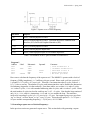
ELE 205 Lab 6 – Spring 2005
Lab 6: Generating a Square Wave of Desired Frequency
1. Objectives:
Learn how to send data to the output ports on 68HC11 EVB.
Generate a square wave of desired frequency.
2. Generating a square wave:
Reading: Sections 2.4.4, 6.1, and 6.2 of M68HC11EVB Evaluation Board User's Manual
A square wave with frequency f = 1 kHz (kilohertz) is shown in the Figure below. This is a periodic
signal with period T = 1/f = 1/1000 = 1 millisecond. The amplitude of the signal is 5 V (volts). This
signal can be generated by making a bit “1” when “high” voltage is required and “0” when “low”
voltage is required. If one is added repeatedly to a binary number, the least significant bit (LSB) of
the result will alternate between 0 and 1. We use this technique of continually incrementing a
number to generate a square wave.
The problem then becomes: write a program that will change the LSB of an accumulator and send
the result to one of the output lines of the EVB. As can be seen in the Table, the EVB has output
ports A-E. They are accessed through connector P1. Connector P1 includes the lines of five ports,
namely Port A, B, C, D, and E, and other signals like E-clock, interrupt request (IRQ), VDD, etc.
Except for Port D, each port has eight pins. Note that Port B is the only port that generates only
output lines. Hence, we will use Port B in this lab. We will generate a square wave with a program
and send the signal to the Port B.
The address for Port B is $1004. This location does not belong to the user programmable space in
the RAM (you can see this on the EVB memory map). Any data that is stored at this location will
appear at the eight pins of Port B. The instruction STAA $1004 will store the value in
Accumulator A into $1004 and thus the eight bits in Accumulator A appear at Port B. The
frequency of the square wave can be measured by connecting the appropriate pins to the
oscilloscope. The pin assignment of the 60-pin connector P1 is shown in Table 6-1 of the EVB
User’s Manual.
We start by writing a program that can do these manipulations. We will use Accumulator A to
increment the value we send to output Port B. We first have to clear Accumulator A, then
continuously increment it and write the result to address $1004. Program 1 (below) performs this
task. Note that the BRA instruction always branches back, so this program has an infinite (never
ending) loop. We can connect an oscilloscope to the appropriate pin on connector Pl to see the
generated square wave, and can calculate the frequency of this signal. All of the square waves will
be observed on bit 0 of Port B (abbreviated “PB0”). You may want to look at the signals generated
on the other bits of Port B, too.
-1-
ELE 205 Lab 6 – Spring 2005
Figure 1: Square wave of l kHz frequency
Pins on P1
Purpose
9-16
Port C, General-purpose I/O lines
20-25
Port D, General-purpose I/O lines. Used with the Serial Communication
Interface (SCI) and Serial Peripheral Interface (SPI).
27-34
Port A, General-purpose I/O lines.
35-42
Port B, General-purpose output lines.
43-50
Port E, General-purpose input or A/D channel input lines
Table 1: Pin numbers of MCU ports available on connector P1
Program 1
Address
Label
Mnemonic
C010
C011
C012
C015
C017
CLRA
INCA
STAA
BRA
SWI
LOOP
FINISH
Operand
$1004
LOOP
Comment
;
;
;
;
;
Clear Accumulator A
Increment Accumulator A
Send ACCA to Port B
Branch back always
We never get here!
How can we calculate the frequency of the square wave? The M68HC11 operates with a clock of
frequency 2 MHz (megahertz), i.e. 2 million cycles per second. Hence each cycle has a period of
1 second/(2 × 106 cycles) = 0.5 µsec/cycle. Therefore, if an instruction takes 4 cycles, it takes 4 ×
0.5 = 2 µsec to execute. The number of cycles each instruction takes can be found in the Instruction
Set Summary (Appendix A in the textbook). From these tables, we see that CLRA takes 2 cycles,
INCA takes 2 cycles, STAA with extended addressing takes 4 cycles, and BRA takes 3 cycles. Hence
the total number of cycles involved in each loop are 2+4+3 = 9 cycles. Note that the loop consists of
only INCA, STAA, and BRA instructions. CLRA and SWI are outside the loop. The total time
involved in executing 9 cycles is 9 × 0.5 µsec/cycle = 4.5 µsec. Our output square wave goes from
“up” to “down”, or from “down” to “up”, every 4.5 µsec. This makes the period T = 2 × 4.5 µsec =
9.0 µsec and the corresponding frequency f = 1/(9.0 µsec) = 0.1111 MHz.
3. Generating a square wave of desired frequency:
In the previous section we generated a square wave. This section deals with generating a square
-2-
ELE 205 Lab 6 – Spring 2005
wave of a desired frequency. We showed the calculations required for computing the total number
of clock cycles in a given loop. To generate a square wave of lower frequency (< 0.1111 MHz), we
need to introduce a “wait loop”, i.e., a sequence of instructions that takes some time to execute but
does nothing. The following assembly program shows one such wait loop.
WAIT LOOP
Address
Label
Mnemonic Operand
Comment
C010
C011
C012
C014
LDX
DEX
BNE
SWI
;
;
;
;
LOOP
FINISH
#$0010
LOOP
load loop counter
Decrement Index Register
Branch till the end of loop
Stop
This wait loop does nothing, but it spends some time executing. Inserting such a loop in Program l,
we can increase the execution time and hence can increase the period of the generated square wave.
Program 2 shows Program 1 modified with a wait loop.
Program 2
Address
C010
C011
C012
C015
C016
C018
C01B
C01C
Label
LOOP
WAIT
FINISH
Mnemonic Operand
Comment
CLRA
INCA
LDX
DEX
BNE
STAA
BRA
SWI
;
;
;
;
;
;
;
;
#$N
WAIT
$1004
LOOP
Clear Accumulator A
Increment Accumulator A
Load Index Register X with a number N
Decrement Index Register
Branch back to wait loop
Send ACCA to Port B
Branch back always
We never get here!
Note that an unknown number N is used in Program 2. For a given frequency we wish to generate,
we must compute the value of N. We compute the execution time involved in executing LOOP by
analyzing the loop WAIT, and the rest of the instructions in loop LOOP with cycle-by-cycle
calculations:
WAIT loop timing:
- N = Total number of times the loop WAIT is executed
- DEX takes 3 cycles.
- BNE takes 3 cycles.
- Total cycles in WAIT loop = 6N.
LOOP loop timing:
- INCA takes 2 cycles.
- LDX takes 3 cycles in immediate addressing mode.
- STAA takes 4 cycles in extended addressing mode.
- BRA takes 3 cycles.
- Total cycles in LOOP loop = 2 + 3 + 6N + 4 + 3 = 6N + 12 cycles
Square wave characteristics:
Period of square wave: T = 2 × (6N + 12) cycles × 0.5 µsec/cycle = 6N + 12 µsec
A desired frequency of f MHz implies: N = (1/f - 12) / 6
-3-
ELE 205 Lab 6 – Spring 2005
The number N calculated from this formula for a desired frequency, fdesired , should be substituted for
N in Program 2. Care should be taken since the resulting N is a real number, not an integer. The
integer value closest to the calculated real number should be chosen. The resulting frequency will
not always equal the desired frequency, fdesired . For example, fdesired = 25 kHz results in N = 4.67; we
choose the closest integer, N = 5. The calculated frequency is fcalc = 23.8 kHz.
A solution to this problem is to introduce more instructions to change the loop timing. A good
choice is the NOP instruction (no operation). This instruction does nothing but use two CPU cycles
(it doesn't change any registers, affect the CCR, etc.). Since it doesn't affect the CPU, it is a good
choice to use in wait loops. If additional instructions are introduced, all the cycle-by-cycle
calculations must be redone since the above formula for N is no longer valid.
Prelab:
1. Create Program 3 from Program 2 by introducing two NOP instructions, the first before the LDX
instruction and the second before the BNE instruction. Redo the cycle-by-cycle calculations and
derive the new expression for N required for a given f.
2. Let fdesired be 16 kHz. Find fcalc for both Program 2 and Program 3 (the one with the additional
NOP instructions). Calculate the percentage difference between the desired frequencies and
calculated frequencies.
3. Code Program 1, Program 2, and Program 3. Make sure AS11 can assemble them without
generating any warnings or error messages. Bring these source files to lab!
Lab Work: Assemble and run Program 1, Program 2, and Program 3. For Program 1, measure the
frequency of the square wave on PB0. For Programs 2 and 3, let fdesired = 16.0 kHz. Measure the
frequency of the square wave on PB0. Also record the wave frequencies on PB1 and PB2.
Lab Report: Show your calculations from prelab and values measured in lab. Make a table for the
results of Program 2 and Program 3. Show the desired frequencies, the calculated frequencies, and
the measured frequencies. Show the percentage difference between the desired and measured
frequencies, and the percentage difference between the calculated and measured frequencies.
Answer the following:
1. Explain the purpose of connector P1 in our lab.
2. List the number of bytes and number of cycles required for executing the instructions MUL,
FDIV, IDIV, and NOP. Note that the number of bytes of an instruction is different from the
number of cycles required to execute the instruction.
3. Compute the time required for executing loop LOOP once in Program 1 if the clock frequency of
the M68HC11 is 5 MHz instead of 2 MHz.
4. Which program gave you the frequency closest to the desired frequency of 16.0 kHz? Why?
5. Derive an expression (mathematically and/or graphically) relating the frequency of the square
wave on bit 1 of Port B (PB1) to the square wave frequency you observed on bit 0 (PB0).
-4-