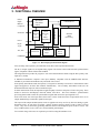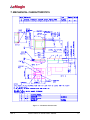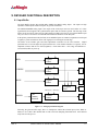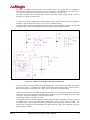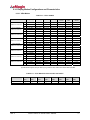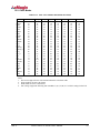
1
SVGA+ Rev3 XL SERIES
852 X 600
ACTIVE MATRIX OLED MICRODISPLAY
USER’S SPECIFICATION
Revision 4
For Part Numbers:
EMA-100309-01
EMA-100310-01
EMA-100311-01
TABLE OF CONTENTS
1.
INTRODUCTION ..................................................................................................................................1
2.
GENERAL CHARACTERISTICS ........................................................................................................2
3.
FUNCTIONAL OVERVIEW..................................................................................................................3
4.
INPUT / OUTPUT DESCRIPTION .......................................................................................................5
5.
ELECTRICAL CHARACTERISTICS ...................................................................................................6
5.1. Analog R, G, B Input Characteristics ................................................................................................ 8
6.
OPTICAL CHARACTERISTICS ..........................................................................................................9
6.1. Measurement Conditions ................................................................................................................ 10
7.
MECHANICAL CHARACTERISTICS................................................................................................11
8.
CLEANING HANDLING AND STORAGE RECOMMENDATIONS ..................................................13
8.3 Static Charge Prevention: ................................................................................................................ 13
8.4 Protection from Dust and Dirt:.......................................................................................................... 14
8.5 Short Term Storage:......................................................................................................................... 14
8.6 Long Term Storage: ......................................................................................................................... 14
9.
DETAILED FUNCTIONAL DESCRIPTION .......................................................................................15
9.1. Input Buffer...................................................................................................................................... 15
9.2. Data Sampling................................................................................................................................. 17
9.3. Pixel Cell ......................................................................................................................................... 17
9.4. Pixel Driver ...................................................................................................................................... 18
9.5. Voltage References......................................................................................................................... 18
9.6. Vertical Sequencer and Row Driver ................................................................................................ 21
9.7. Horizontal & Burn-in Sequencers.................................................................................................... 22
9.8. Burn-in compensation Sequencer................................................................................................... 23
9.9. Clock Recovery ............................................................................................................................... 24
9.10. Sync Processor ............................................................................................................................. 24
9.11. Serial Interface .............................................................................................................................. 24
9.11.1. Sequential Read/Write Operation ...........................................................................................................25
9.12. Power On sequence...................................................................................................................... 26
9.13. Power Down Modes ...................................................................................................................... 26
9.13.1. Automatic Power Down Mode ................................................................................................................26
9.13.2. Manual Power Down Mode.....................................................................................................................26
9.14. Display Modes Configurations and Characteristics ...................................................................... 27
9.14.1. VESA Modes ..........................................................................................................................................27
9.14.2. Interlaced Video Modes ..........................................................................................................................28
9.14.3. Zoom & 16:9 Modes ...............................................................................................................................28
10.
REGISTER MAP SUMMARY ............................................................................................................29
11.
DETAILED REGISTER DESCRIPTION ............................................................................................31
12. REGISTER TABLE CONFIGURATION.............................................................................................42
12.1. VESA Modes ................................................................................................................................. 42
12.2. Other Modes.................................................................................................................................. 43
13.
APPENDIX A: MICRODISPLAY CARRIER BOARD ELECTRICAL DIAGRAM..............................44
14.
APPENDIX B: COMPOSITE SIGNAL INPUT CONNECTIONS .......................................................45
15.
APPENDIX C: REVISION HISTORY .................................................................................................46
Rev 4
SVGA+ Rev3 XL Series User’s Manual
i
LIST OF FIGURES
Figure 3-1. Microdisplay functional block diagram ...................................................................................................................... 3
Figure 7-1. Mechanical Characteristics....................................................................................................................................... 11
Figure 9-1. Analog Inputs Block Diagram .................................................................................................................................. 15
Figure-9-2. Input Multiplexer Block Diagram ............................................................................................................................ 16
Figure 9-3. Dual Sample & Hold Block Diagram ....................................................................................................................... 17
Figure 9-4. OLED I-V Characteristic (Log and Linear scale) .................................................................................................... 18
Figure 9-5. Sample Circuit Designs Using External References ................................................................................................ 19
Figure 9-6. Luminance as a Function of Vbh ............................................................................................................................. 20
Figure 9-7. Typical Contrast Ratio as a Function of Vblack ...................................................................................................... 21
Figure 9-8. Serial Interface Protocol ........................................................................................................................................... 25
Figure 10-1. Register Map Summary ........................................................................................................................................... 30
Figure 13-1. Microdisplay Carrier Board Electrical Diagram .................................................................................................... 44
LIST OF TABLES
TABLE 2-1. GENERAL CHARACTERISTICS ........................................................................................................................ 2
TABLE 3-1. SVGA+ MICRODISPLAY VIDEO FORMATS ................................................................................................... 4
TABLE 4-1. INPUT-OUTPUT DESCRIPTION......................................................................................................................... 5
TABLE 5-1. ABSOLUTE MAXIMUM RATINGS..................................................................................................................... 6
TABLE 5-2. RECOMMENDED OPERATING CONDITIONS ............................................................................................... 6
TABLE 5-3. DC CHARACTERISTICS DC CHARACTERISTICS ........................................................................................ 7
TABLE 5-4. AC CHARACTERISTICS ...................................................................................................................................... 7
TABLE 5-5. INPUT CHARACTERISTICS................................................................................................................................ 8
TABLE 6-1. EMA-100310-01 COLOR MICRODISPLAY OPTICAL CHARACTERISTICS.............................................. 9
TABLE 6-2. EMA-100309-01 MONOCHROME WHITE MICRODISPLAY OPTICAL CHARACTERISTICS .............. 9
TABLE 9-1. INPUT MULTIPLEXER SELECTION CONTROLS........................................................................................ 16
TABLE 9-2. VERTICAL SEQUENCER CONTROLS............................................................................................................ 21
TABLE 9-3. MICRODISPLAY ROW SEQUENCE ................................................................................................................ 22
TABLE 9-4. MICRODISPLAY HORIZONTAL MODE CONTROLS ................................................................................. 23
TABLE 9-5. VESA MODES ....................................................................................................................................................... 27
TABLE 9-6. SYNCHRONIZATION PULSES POLARITY.................................................................................................... 27
TABLE 9-7. INTERLACED VIDEO MODES.......................................................................................................................... 28
TABLE 9-8. ZOOM AND 16:9 VIDEO MODES...................................................................................................................... 28
TABLE 9-9. ZOOM AND 16:9 MODES SYNCHRONIZATION PULSES POLARITY ..................................................... 28
TABLE 12-1. VESA MODES REGISTER SETTINGS ............................................................................................................ 42
TABLE 12-2. NON-VESA MODES REGISTER SETTINGS ................................................................................................. 43
TABLE 15-1. MINIMUM CONNECTIONS REQUIRED FOR COMPOSITE INPUT ....................................................... 45
Rev 4
SVGA+ Rev3 XL Series User’s Manual
ii
1. INTRODUCTION
eMagin’s SVGA+ Rev3 OLED Microdisplay continues the SVGA+ series of microdisplays with a resolution of
852x3x600 pixels and compatibility with multiple video sources. The SVGA+ Rev3 XL OLED Microdisplay is
nearly identical to the SVGA+ Rev2 XL OLED Microdisplay except the Rev3 requires input for the Vbh and
Vbl terminals (previously generated internally). This change allows for a more monotonic behavior of the
luminance as a function of temperature, improving the integration of the SVGA+ microdisplay in rugged
environment compatible systems.
This series of microdisplays was dubbed "SVGA+" (Super Video Graphics Array plus) because they 52 more
display columns than a standard SVGA display.. This design permits users to run either (1) standard SVGA
(800 x 600 pixels) to interface to the analog output of many portable computers or (2) 852 x 480, using all the
data available from a DVD player in a 16:9 wide screen entertainment format. The SVGA+ can be made as a
full-color or monochrome microdisplay primarily for high-performance and large-view consumer OEM
products such as games, video/data head-wearable displays, digital cameras, video cameras and other portable
electronics applications. The display also has an internal NTSC and PAL monochrome video decoder suitable
for low power night vision systems. This product is designed to interface with most portable personal
computers.
See Chapter 8, “Handling,”
prior to use of displays
(with or without glass
covers).
NOTE
This specification applies to the following SVGA+ Rev3 XL Series OLED microdisplay models:
Color:
White monochrome:
Green monochrome:
EMA-100310-01
EMA-100309-01
EMA-100311-01
NOTE: Please refer to the Defect Criteria Document C15-100000-xx for specifics on Defect types
Rev 4
SVGA+ Rev3 XL Series User’s Manual
1
2. GENERAL CHARACTERISTICS
TABLE 2-1. GENERAL CHARACTERISTICS
Parameter
Format
Specification1
852 (x3) x 600 pixels
Color Pixel Aspect Ratio
Square
Color Pixel Pitch
15 µm
Color Pixel Arrangement
R, G, B Vertical Stripe
Viewing Area
12.78 x 9 mm
Mechanical Envelope
19.78 x 15.2 x 5 mm
Weight
1.8 grams
White Chromaticity
x = 0.30 ±0.03, y = 0.35 ±0.03
Gray Levels
Up to 256 per primary color
Uniformity
> 85% (2)
Contrast Ratio
≥100:1 Intrinsic (Measured per VESA FPDM Standard)
White Luminance Maximum
≥ 150 cd/m2 (front luminance), SVGA 60Hz VESA mode
Video Inputs
R, G, B Inputs
Monochrome Input
0 to 0.7 V, compatible with VESA VSIS standard
0 to 1.0 V, compatible with SMTPE-170M & PAL
Video Signal Bandwidth
56 MHz maximum (VESA mode), up to 85Hz frame rate
13 MHz minimum (SMPTE-170 mode), 30 Hz frame rate
Control & Serial Interface
Digital 3.3 V CMOS
Power Interface
Logic/Analog Supply (Vdd)
Van
Vcommon
3.3 Volts DC @ 50 mA maximum
4.0 Volts DC @ 50 mA maximum
-3.0 Volts DC @ 50 mA maximum
Operating Ambient Temperature*
-40°C to +65°C
Storage Temperature
-55°C to +90°
Humidity
85%RH non-condensing
Note 1: The above data represents consumer and commercial performance specifications, measured at 20°C.
Performance will vary at temperatures above or below 20°C. Operation may be possible outside this temperature
ranges, especially for short term use, but such use is considered outside of the basic commercial specification range.
For additional information about special operating conditions and methods of test, contact eMagin Technical
Support.
Note 2: At 100% of gray level brightness and 60 Cd/m2 luminance. Luminance uniformity measured between the
nominal values of five 1000 pixel zones located in the four extreme corners and the center zone of display.
Rev 4
SVGA+ Rev3 XL Series User’s Manual
2
3. FUNCTIONAL OVERVIEW
MONO
Composite
Serial Bus
Input buffer
Gain-Offset
control
Host
Interface
&
Registers
Power
Column Driver
Clock
Recovery
&
Phase
Interpolator
Row Driver
R,G,B
Inputs
852x600
RGB
Pixel Array
Hsync
Vsync
Vbl, Vbh
Voltage
References
Control
Logic
Power
Down
Control
COMMON
Figure 3-1. Microdisplay functional block diagram
Four (4) analog video inputs are provided: Red, Green, Blue, and Composite Monochrome.
The R, G, B input signals are dc-coupled analog signals with external vertical and horizontal synchronization
signals, compatible with the VESA VSIS standard.
The integrated circuit provides for progressive scan color and monochrome modes using the three primary color
inputs (R, G, and B).
A dedicated monochrome composite video input (MONO), compatible with the SMPTE-170M and PAL
standards is provided for monochrome-only interlaced video sources.
In the primary monochrome mode, the input R, G, B signals are internally converted to a monochromatic white
signal and applied to all three data channels simultaneously. The secondary monochrome mode uses the
dedicated interlaced composite video monochrome input.
In either monochrome mode, the input data is applied equally to the three sub-pixels of each color group. These
modes are meant for microdisplays delivered without color filters. The circuit includes a synchronization
processing function that extracts the synchronization signals and restores the input signal dc level.
In the color mode, each color input data is delivered in a raster format and fed to an input buffer and a set of
sample and hold stages connected in parallel to the input.
The output of the sample and hold (SAH) circuits is applied to the array on a line by line basis during a typical
horizontal period. At each pixel cell resides a storage element (capacitor) which is used to control a current
source. Gray scale is achieved by generating different current levels through the pixel cell driver circuit. The
array is addressed one row at a time as are conventional flat panel displays.
Two external voltage references are required to provide for setting the luminance level.
Rev 4
SVGA+ Rev3 XL Series User’s Manual
3
The SVGA+ microdisplay has built-in settings for the following video formats:
TABLE 3-1. SVGA+ MICRODISPLAY VIDEO FORMATS
Format (columns x rows)
640 x 480 Color
800 x 600 Color
640 x 480 Monochrome
640 x 480 Monochrome
800 x 600 Monochrome
800x 600 Monochrome
852 x 480 Color
852 x 600 Color 4
Name
VGA
SVGA
SMPTE-170M
SMPTE-170M
PAL3
PAL3
16:9 Format
Zoom
Input Mode
Progressive Scan
Progressive Scan
Interlaced
Interlaced
Interlaced
Interlaced
Progressive Scan
Progressive Scan
Output (Display) Mode
Progressive Scan
Progressive Scan
Interlaced Scan
Pseudo Interlaced Scan
Interlaced Scan
Pseudo Interlaced Scan
Progressive Scan
Progressive Scan
NOTES:
1: All progressive scan input modes should use the R, G, B video inputs. All interlaced input modes should use
the MONO composite video input. However, all progressive scan color modes are available in the primary
monochrome which can be activated through the registers. Other modes are also available..
2: A pseudo-interlaced scan is equivalent to a line-doubling scan during which two adjacent rows are enabled at
the same time. A one-row offset occurs every even field.
3: 800 x 600 Monochrome modes are compatible with all forms of PAL/CCIR except for PAL M. PAL M uses
525 lines, thus 640 x 480 Monochrome modes should be used.
4: The Zoom mode is the power-on default operating mode of the microdisplay.
Selection between the non-interlaced and interlaced modes is done through a register set via the on-chip serial
interface. The power-up default is a non-interlaced Zoom 60Hz mode.
The serial interface also provides for user adjustments such as contrast, brightness, PLL parameters, display
orientation (an externally hardwired control is also provided).
Standard VESA analog video modes do not carry the video clock, which has to be regenerated on chip. A clock
recovery circuit based on a digital phase locked loop circuit provides a recovered pixel clock. The PLL has
default power-on settings, which can be overridden via the serial interface.
An external video clock input (VCLK) is also available and is enabled/disabled via the serial interface. Default
power-up mode is VCLK input disabled.
Rev 4
SVGA+ Rev3 XL Series User’s Manual
4
4. INPUT / OUTPUT DESCRIPTION
Connector Part Number: Hirose DF12D (3.0)-30DP-0.5V
TABLE 4-1. INPUT-OUTPUT DESCRIPTION
Pin #
1
2
Name
VDD
/RESET
Type
Power
I
3
4
SCL
SDA
I
I/O
5
6
PWM
L/R
O
I
7
U/D
I
8
9
10
11
12
13
14
15
16
17
18
19
20
21
22
23
24
25
SERADD
VAN
COMMON
GND
VBLACK
VBH
VBL
N/C
N/C
GND
RED
GND
GREEN
GND
BLUE
GND
MONO
VS
I
Power
Power
Power
I/O
I
I
Open
Open
Power
I
Power
I
Power
I
Power
I
I
26
HS
I
27
VCLK
I
28
29
30
N/C
N/C
N/C
Open
Open
Open
Rev 4
Description
Power input for the analog and logic circuits 3.3V nominal
System Reset Input (active low). Used to asynchronously reset the
entire microdisplay. 100 µs minimum active.
Clock port for the serial interface. 400 KHz Max.
Data port for the serial interface. Open collector output with 2.2K onboard pull-up resistor
Logic output. Reserved for test.
Left/Right logic input. Used to configure the starting pixel position (left
or right)
Up/Down logic input. Used to configure the starting row position (top
or bottom)
Serial Interface LSB address bit. Must be connected.
Input power for Pixel Array (4.0 VDC nominal).
Common display terminal. (- 3.0 VDC nominal).
Microdisplay power return terminal
Internal Reference Voltage Monitor Output / External Input
External Reference Voltage Input
External Reference Voltage Input
Not Used
Not Used
IC power return terminal
Analog video signal inputs. 0 to 0.7 V peak to peak.
IC power return terminal
Analog video signal inputs. 0 to 0.7 V peak to peak
IC power return terminal
Analog video signal inputs. 0 to 0.7 V peak to peak
IC power return terminal
Composite Video input. 1.0 V peak to peak nominal.
Vertical Sync logic input. TTL level. Used with non-composite video
input
Horizontal Sync logic input used with non-composite video input. TTL
level.
Video data input clock (logic input). Used when the internal clock
recovery circuit is disabled. TTL level.
Not Used
Not Used
Not Used
SVGA+ Rev3 XL Series User’s Manual
5
5. ELECTRICAL CHARACTERISTICS
TABLE 5-1. ABSOLUTE MAXIMUM RATINGS
Parameter
VDD
VAN
Vcommon
Vbl
Vbh
Vblack
VI
VO
Tst
Tj
Ilu
Vesd
Front End Power Supply
Array Power Supply
Common electrode bias
External Reference
External Reference
External Black Reference
Input Voltage Range
Output Voltage Range
Storage Temperature
Junction Temperature
Latch up current
Electrostatic Discharge –
Human Body Model
Min
-0.3
-0.3
-5
0
0
0
-0.3
-0.3
-55
-25
Typ.
2
2.2
3.6
Max.
4.6
4.6
0
Van
Van
Van
VDD+0.3
VDD+0.3
+90
+125
+100
±2000
Unit
VDC
VDC
VDC
VDC
VDC
VDC
VDC
VDC
°C
°C
MA
V
Stresses at or above those listed in this table may cause permanent damage to the device. This is a stress rating
only and functional operation of the device at these or any other condition above those indicated in the
following tables is not implied. Exposure to absolute maximum rated temperatures or voltages in the chart
below for extended periods may affect device reliability. Prolonged exposure to high temperatures will shorten
the luminance half-life. Protection diodes are suggested between Vcommon and ground to protect against power
supply spikes.
TABLE 5-2. RECOMMENDED OPERATING CONDITIONS
Parameter
VDD
VAN
Vcommon
Vbl
Vbh
Vblack
Tst
Ta*
PD
Front End Power Supply
Array Power Supply
Common electrode bias
External Reference
External Reference
External Black Reference
Storage Temperature
Ambient Operating Temp.
Power Dissipation
Min
3.0
3.8
-5
1.4
1.6
3.4
-55
-40
Typ.
3.3
4.0
-3.0
1.6
1.8
3.6
+25
Max.
3.6
4.2
0
2.0
2.600
3.8
+90
+65
450
Unit
VDC
VDC
VDC
VDC
VDC
VDC
°C
°C
mW
Note*: The above data represents commercial performance specifications, measured at 20°C. Performance will
vary at temperatures above or below 20°C. Operation at higher or lower temperatures is possible but may
require compensation via biasing to maintain the 20°C optimum performance. Half-life is reduced at high
temperatures. Operation may be possible outside the temperature ranges specified in Table 5-2, especially for
short term use, but such use is considered outside the basic specification range. Operation outside the
recommended operating conditions will void any warranty.
The consumer OEM specification for acceptable operating and storage temperature range is different from the
above chart; refer to the SVGA-3D specifications for this parameter.
Rev 4
SVGA+ Rev3 XL Series User’s Manual
6
Contact eMagin customer service regarding potential use of the display under other conditions. Warranties for
use under other operating conditions require formal written documentation specifically extending the warranty
to these conditions. Statement of potential acceptable use under alternate conditions by company personnel
does not constitute a warranty extension.
TABLE 5-3. DC CHARACTERISTICS DC CHARACTERISTICS
Ta = 20°C, GND = 0V, VDD = +3.3V, VAN = +4V, Vcommon =-3.0
Parameter
Vil
Vih
Vol
Voh
Ivbh, Ivbl
Ivblack
V MONO 1
V R,G,B 2
Pd Van
Pd VDD
Pd VCOM
Digital input low level
Digital input high level
Digital output low level
Digital output high level
External Reference Current
External Black Reference Current
MONO Analog input dc level
VESA Inputs signal level
Average Van Power Dissipation
(SVGA Mode 60 Hz refresh rate)
Average VDD Power Dissipation
(SVGA Mode 60 Hz refresh rate)
Average VCOMMON Power
Dissipation (@ -3.0V)
Min
GND-0.3
2.0
2.4
-1.2
Typ.
Max.
1
VDD+ 0.3
0.5
0.18
0
60
0.3
0.05
1.0
0.7
150
Unit
VDC
VDC
VDC
VDC
mA
mA
VDC
VDC
mW
140
180
mW
50
150
mW
0
0
Notes:
1: The RED, GREEN and BLUE inputs are CMOS inputs. No termination other than those required by the
driving source and cable characteristics are required
2: The MONO channel includes a dc restore circuit. A non-polarized ac coupling capacitor is required for
proper operation.
TABLE 5-4. AC CHARACTERISTICS
Ta = 20°C, GND = 0 V, VDD= +3.3V, Van = +4.0V, VCOMMON =-3.0
Symbol
Fvclk
Ths
Thsw
Tvs
Tvsw
Trst
Cpwm
Cav
Parameter
Video Clock Frequency
Horizontal Sync frequency
Hsync Pulse Width
Vertical Sync Frequency1
Vsnc Pulse Width
Reset Pulse Width
PWM Output Load
Analog input capacitance
Min
10
15.7
2
30
2
100
Typ.
-
85
4
5
Max.
56.25
53
8
8
Unit
MHz
KHz
Tclk
Hz
Tclk
µs
pF
Pf
Note 1: Maximum refresh rate for SVGA mode is 85 Hz. For interlaced mode the frame rate may be as low as
30 Hz (SMPTE Modes)
Rev 4
SVGA+ Rev3 XL Series User’s Manual
7
5.1. Analog R, G, B Input Characteristics
Input Characteristics (per VESA VSIS rev 1.0)
TABLE 5-5. INPUT CHARACTERISTICS
Parameter
Max Luminance1
Min Luminance1
Video Channel Rise/Fall Time
Max
Video Channel Rise/Fall Time Min
Settling Time Max
Monotonic
Resolution
Integral Linearity Error
Differential Linearity Error
Video Channel to Video
Channel Mismatch
Noise injection ratio
Video Channel to Video
Channel Output Skew
Overshoot/ Undershoot
Value
0.700 Volts - 0.035 Volts/ +0.07 Volts
0.000 Volts
50% of minimum pixel clock
period
20 % of minimum pixel clock
period
30% of minimum pixel clock
period
Yes
1 LSB
+/- 1 LSB
+/- 1 LSB
6% of any output voltage over the full
voltage range
0.5 % of Max Luminance Voltage
25% of minimum pixel clock
period
+/-12% of step function voltage level over
the full voltage range
Comment
All Sources
DC to Max Pixel
Frequency
1.5 X the rise time duration
Note 1: With respect to GND.
Rev 4
SVGA+ Rev3 XL Series User’s Manual
8
6. OPTICAL CHARACTERISTICS
TABLE 6-1. EMA-100310-01 COLOR MICRODISPLAY OPTICAL CHARACTERISTICS
Conditions: Ta = +20°C, GND = 0 V, VDD= +3.3V, Van = +4.0V, Vcommon =-3.0
Symbol
L
CR
U
CIE White
Gray
Levels
Refresh
Rate1
Pixel
Cell
Fill Factor
Parameter
Front Luminance
White to Black Contrast Ratio
Area Uniformity
X
Y
Ng
Progressive scan mode
Interlaced scan mode
Sub Pixel Width Pitch
Sub Pixel Height Pitch
% Emissive Area vs. total subpixel area
Min
0.5
300:1
80%
0.27
0.29
64
Typ.
140
90%
0.32
0.34
256
Max.
400
100%
0.37
0.38
-
40
30
5
15
62
85
85
59
Unit
Cd/m2
Levels
Hz
Hz
µm
µm
%
65
Note 1: Specification refers to value producing no visible image flicker
TABLE 6-2. EMA-100309-01 MONOCHROME WHITE MICRODISPLAY OPTICAL
CHARACTERISTICS
Symbol
L
CR
U
CIE
Gray
Levels
Refresh
Rate1
Pixel
Cell
Fill Factor
Parameter
Front Luminance
White to Black Contrast Ratio
Area Uniformity
X
Y
Ng
Progressive scan mode
Interlaced scan mode
Sub Pixel Width Pitch
Sub Pixel Height Pitch
% Emissive Area vs. total subpixel area
Min
0.5
300:1
80%
0.27
0.295
64
Typ.
900
90%
0.32
0.345
256
Max.
1800
100%
0.37
0.395
-
40
30
5
15
62
85
85
59
65
Unit
Cd/m2
Levels
Hz
Hz
µm
µm
%
Note 1: Specification refers to value producing no visible image flicker
Rev 4
SVGA+ Rev3 XL Series User’s Manual
9
TABLE 6-3. EMA-100311-01 MONOCHROME GREEN MICRODISPLAY OPTICAL
CHARACTERISTICS
Symbol
L
CR
U
CIE
Gray
Levels
Refresh
Rate1
Pixel
Cell
Fill Factor
Parameter
Front Luminance
White to Black Contrast Ratio
Area Uniformity
X
Y
Ng
Progressive scan mode
Interlaced scan mode
Sub Pixel Width Pitch
Sub Pixel Height Pitch
% Emissive Area vs. total subpixel area
Min
1
100:1
80%
0.0
0.50
64
Typ.
1500
90%
0.23
0.55
256
Max.
3000
100%
0.30
0.66
-
40
30
5
15
62
85
85
59
65
Unit
Cd/m2
Levels
Hz
Hz
µm
µm
%
Note 1: Specification refers to value producing no visible image flicker
Optical characteristics are measured in accordance with the VESA Flat Panel Display Measurement Standard,
Rev 1.0 (A copy of the standard is available at the VESA website: www.vesa.org).
6.1. Measurement Conditions
Luminance, contrast and chromaticity measurements are performed in a dark ambient environment at room
temperature, on a dedicated automated test bench.
The reference used for the luminance measurement is the OLED current density, set to 20 mA/cm2. This
reference is purely for reference purposes and corresponds approximately to the typical luminance value.
In order to account for possible leakage effects, the OLED current, measured at the Vcommon terminal, is
first measured when the video input has been set to black. The Vcommon current is then recorded (dark
current) and the video input is set to white (maximum video input level). The Vcommon current is then
adjusted to add exactly 20 mA/cm2 to the dark current. The “white” luminance is then measured, as well as
the color coordinates.
The contrast is then obtained by taking a luminance measurement with the video inputs set to black without
adjusting any other parameter.
Minimum Luminance is defined as the lowest luminance level for which a 100:1 contrast ratio is
measurable.
Maximum Luminance is defined as the maximum luminance the microdisplay can provide while keeping
the black level (0V data input) at or below 1 cd/m2. In order to reach the maximum value mentioned in the
tables above, it will be necessary to adjust the VCommon input to a lower level (typically close to -4.5V).
The minimum and maximum luminance levels are obtained by adjusting the external voltage reference Vbh
and Vbl being kept at a fixed level (See section VOLTAGE REFERENCES page 9).
Rev 4
SVGA+ Rev3 XL Series User’s Manual
10
7. MECHANICAL CHARACTERISTICS
Figure 7-1. Mechanical Characteristics
Rev 4
SVGA+ Rev3 XL Series User’s Manual
11
Connector J1
Manufacturer:
Manufacturer Part Number:
Hirose
DF12D (3.0)-30DP-0.5V
Mating Connector Information
Manufacturer:
Manufacturer Part Number:
Weight:
Hirose
DF12A(3.0)-30DS-0.5V
1.9 g (nominal)
Printed Circuit Board Material:
Printed Circuit Board Tolerances:
FR4
± 0.8 mm (both axes)
Rev 4
SVGA+ Rev3 XL Series User’s Manual
12
8. CLEANING HANDLING AND STORAGE RECOMMENDATIONS
8.1 Cleaning:
When cleaning the displays we recommend the use of TECH-SPEC lens cleaner, manufactured by Edmund
Optics Inc. and Alpha wipes 1010
8.2 General handling considerations:
• Do not expose the display to strong acids, bases, or solvents.
• Do not expose the display surface to UV or other strong ionizing radiation
• Temperatures in excess of the specified operating and storage range can cause irreversible damage to the display.
• Do not allow sharp objects to contact the exposed regions of the silicon display chip.
• Avoid immersion of the display in any liquid.
• The glass cover slip protects the display surface from most forms of damage and may be cleaned using
techniques appropriate for fine lenses.
• Avoid applying force to the glass relative to the display chip in compressive, tensile, and sheer directions.
Fig. 3 Best method of handling the displays
Fig. 4 Avoid this method of display handling
8.3 Static Charge Prevention:
The microdisplay is sensitive to electro-static discharge damage. The following measures are
recommended to minimize ESD occurrences:
• When handling the microdisplay, operated under a flow of ionized air to discharge the panel
• Use a conductive wrist strap connected to earth ground via a 10 M-Ohm resistor.
• Wear non-chargeable clothes
• Keep stored displays away from charged materials
Rev 4
SVGA+ Rev3 XL Series User’s Manual
13
8.4 Protection from Dust and Dirt:
It is also recommended that all display handling operations take place in a clean environment. The use of
ionized nitrogen gas is the preferred method of removing particles from the surface.
8.5 Short Term Storage:
For short term storage (one to two weeks or less), the displays should be kept in their original container at room
ambient and the typical controlled office environment.
8.6 Long Term Storage:
For displays that will be stored for a longer period (a few weeks and up), it is recommended to keep displays
stored in a dry environment near or at room ambient (20ºC typically) whenever possible prior to installation into
an optical subsystem.
There are several ways to achieve this:
- Dry storage cabinet
- Dry Nitrogen cabinet
- Nitrogen sealed bag
- Vacuum sealed bag with desiccant
Rev 4
SVGA+ Rev3 XL Series User’s Manual
14
9. DETAILED FUNCTIONAL DESCRIPTION
9.1. Input Buffer
The Input Buffer assumes DC-coupled RED, GREEN and BLUE analog inputs. The inputs are high
impedance CMOS inputs and do not require any special termination.
The MONOCHROME analog input is the output of the Video Sync Processor and consists of a video
signal that has been stripped of the synchronization pulses and dc restored to ground. The first stage of the
buffer circuit provides for removal of the CRT gamma provided by the host (for use with the MONO input
only) as well as a correction to accommodate the internal non-linearities of the data path.
In the primary monochrome mode, the Red, Green and Blue inputs are summed (weighted sum with equal
weights) to yield a monochrome white video signal prior to entering the second stage.
The buffer circuit includes gain and offset adjustments controlled via the serial interface. Digital
potentiometers are used to adjust the signal characteristics. Each channel includes two registers, one for
amplitude (contrast) and one for offset (brightness). Each control has a ± 50% range and defaults to 1
(Gain) and 0 (Offset) at power up.
RGAIN[7:0]
ROFF[6:0]
Gain &
Offset
RED
GGAIN[7:0]
GREEN
R
GOFF[6:0]
Gain &
Offset
BGAIN[7:0]
BLUE
G
BOFF[6:0]
Gain &
Offset
B
Weighted
Sum
W
MGAIN[7:0] MOFF[6:0]
MONO
CRT
Gamma
Removal
Gain &
Offset
M
Figure 9-1. Analog Inputs Block Diagram
Following the gain and offset stage, three 3:1 multiplexers channel the selected input (Color, White or
Mono) to one of three data channels that are fed to the Data Sampling functional block. Each channel
maps into 852 cells per row.
Rev 4
SVGA+ Rev3 XL Series User’s Manual
15
The input selection is controlled by the VMODE register, accessible via the serial interface. The lower
two bits, COLSEL1 and COLSEL0, are used.
TABLE 9-1. INPUT MULTIPLEXER SELECTION CONTROLS
COLSEL[1]
0
0
1
1
COLSEL[0]
0
1
0
1
MODE
Color
White
Composite
Color
Mux1 Out
R
W
M
R
Mux2 Out
G
W
M
G
Mux3 Out
B
W
M
B
R
3:1 Analog
Mux1
G
B
W
3:1 Analog
Mux2
To Data
Sampling
3:1 Analog
Mux3
M
COLSEL[1:0]
Figure-9-2. Input Multiplexer Block Diagram
Rev 4
SVGA+ Rev3 XL Series User’s Manual
16
9.2. Data Sampling
The output of the multiplexers is fed to multiple dual sample and hold stages. The design approach is a
pipeline mode where the raster line input data is sampled then held to allow for propagation to the relevant
pixel cell, while allowing for the sampling to continue uninterrupted using the second sampling capacitor.
The stages are optimized to achieve the best balance between low power (via bandwidth reduction and
minimum loading of the buffer) and performance (uniformity, noise and internal propagation delays).
S1
S2
FROM BUFFER
TO PIXEL DRIVER
/S1
/S2
Figure 9-3. Dual Sample & Hold Block Diagram
The analog switches are designed to minimize charge injection and dynamic power dissipation.
The sample and hold amplifier is a unity gain element with low fan out requirements. Its output is fed
directly to the pixel driver circuit. The sequence controlling which SAH is being selected is generated by
the column sequencer block. This includes start and end of active video sampling.
9.3. Pixel Cell
There are 2,556 pixel cells (852 x 3) per active row (600active rows). Each cell is a 5 x 15-micron
rectangle, yielding a 15 x 15-micron square color group (RGB).
The pixel cell output stage is a current source configured around a PMOS transistor. The current flows
from the VAN power input to the OLED’s anode terminal. The OLED is typically represented as a diode.
OLEDs generate an amount of light that is proportional to the current density flowing through the device.
Rev 4
SVGA+ Rev3 XL Series User’s Manual
17
OLED I-V Curve
OLED I-V Curve
100
80
70
10
60
Current (mA)
Current (mA)
1
0.1
50
40
30
20
0.01
10
0.001
0
0
2
4
6
8
10
12
0
2
Voltage (V)
4
6
8
10
12
Voltage (V)
Figure 9-4. OLED I-V Characteristic (Log and Linear scale)
The pixel cell operates at VAN power to maximize the dynamic range of the display technology as well as
accommodate its life-dependent voltage characteristic.
The cathodes of all OLED pixels are electrically connected to the COMMON pin via an internal electrode
that surrounds the array.
9.4. Pixel Driver
The pixel driver block buffers the sampled signal to an output tuned to the array characteristics. There are
as many pixel drivers as there are dual SAH stages.
At the beginning of each video line, the pixel driver output is reset to the black level. This will ensure a
consistent reference level on the data lines and reduce the impact of potential residual charges.
The Pixel driver is designed around a current source operated in the sub-threshold region in order to
output the low current required by the OLED to generate modulated light.
The driver works in two phases, a programming phase and a run phase
During the programming phase, which lasts for one row period, the output of the sample and hold charges
the pixel storage capacitor with a current approximately 100 times greater than the value needed for light
emission. This provides for enough settling time over the specified refresh rate range.
During the run phase, which lasts for one entire frame period minus one row period, the pixel driver output
current is scaled down by switching the drive transistor into its sub-threshold operation region. This is
achieved by changing the storage capacitor reference level.
This method preserves the dynamic range as well as the linearity of the overall transfer function.
9.5. Voltage References
Three reference voltage levels are used in the pixel driver circuit: Vblack, Vbl and Vbh.
Vblack can be generated internally or provided externally. Vbl and Vbh require external bias.
Rev 4
SVGA+ Rev3 XL Series User’s Manual
18
The power on condition for the Vblack is the internal reference. This setting can be overridden by
powering down the internal references after power-up using register 17h (PDWN) bits 4,5, and 6 (Set to 1
for power down), and register 18h (ATB) bit 7 (Set to 1 to allow use of register 17h).
The output impedance of the internal Vblack reference generator is high enough that an override is
possible even without powering it down.
Care must be taken when designing an external voltage reference circuit for Vbl and Vbh.. An application
schematic is provided below that can serve as a basis for a production design.
A different approach relying on operational amplifiers in lieu of shunt regulators is possible. A4.7 K-Ohm
pull down resistor is then recommended at both Vbl and Vbh inputs to maximize stability.
Figure 9-5. Sample Circuit Designs Using External References
Vbl is the reference level used during the programming phase of the pixel driver operation. During this
phase the pixel driver is programmed at a higher current value than needed for image restitution. This is
done for settling time reasons. This level is active one row per frame for each pixel driver.
Vbh is the reference level used during the light emission phase of the pixel driver operation which lasts
most of the video frame. Vbh switches the pixel driver current range down by roughly 100 times in order
to bring it to the typical operating levels required by the OLED.
Vbh operates typically at 200 mV above Vbh.
Varying Vbh causes the current through the OLED to change and thus the luminance to change. Since this
is a global input, it affects the entire display and therefore can be used for dimming control. The
relationship between Vbh and the luminance is exponential. The dimming range can be over 1000:1 over
200 mV. One consequence of this relationship is the high sensitivity to Vbh. A few millivolts will yield a
large luminance variation.
Rev 4
SVGA+ Rev3 XL Series User’s Manual
19
Note that bringing Vbh less than 100 mV above Vbl will result in a washed out display with no
modulation as well as a high luminance level that will accelerate the display aging.
The graph below illustrate the luminance response as a function of Vbh for a color microdisplay. For this
measurement, Vbl = 2.0V
Luminance vs. Vbh
1000
Luminance (cd/m2)
100
10
1
0.1
0.01
2.1
2.15
2.2
2.25
2.3
2.35
2.4
2.45
2.5
2.55
Vbh (Volt)
Figure 9-6. Luminance as a Function of Vbh
Vblack is a reference level used to reset the pixel driver to the black level at the beginning of each line.
Using an externally generated voltage level can improve the display contrast ratio significantly, albeit with
a higher variability from display to display. Adjusting Vblack only affects the black level (0V video input)
and has no impact on the maximum luminance.
The internal Vblack reference circuit output is nominally 3.45V.
An optimum value for an externally generated Vblack is 3.60 V.
The reference is a dc level reference that requires very little current (less than 50 micro Amperes).
The graph below shows the typical contrast ratio (dark ambient measurement) as a function of Vblack for
the SVGA+ Rev3 Color microdisplay. Two curves were taken for two different values of Vbl for
information purposes.
For reference when Vbl = 1.6V, Vbh= 1.805V. When Vbl = 2.0V, Vbh = 2.218V
Rev 4
SVGA+ Rev3 XL Series User’s Manual
20
SVGA Color Contrast vs Vblack
600
500
CR units
400
Part#1 Vbl=1.6V
300
Part#1 Vbl=2.0V
200
100
0
3.2
3.3
3.4
3.5
3.6
3.7
3.8
3.9
4
Vblack (Volts)
Figure 9-7. Typical Contrast Ratio as a Function of Vblack
9.6. Vertical Sequencer and Row Driver
The row driver is designed around a 600-stage shift register. For nomenclature and reference purposes,
Row # 1 is set arbitrarily to be the top row when viewing the display with the I/O pads on the left.
The shift register is bi-directional. The direction is set by the U/D external input or by bit 5, VSCAN, in
the VMODE registers. The priority is set by bit 6, VSCANS of the same register. When VSCANS = 0,
the external input has priority. When VSCANS = 1, VSCAN has priority. When U/D = GND or VSCAN
= 0, the display is scanned from top to bottom (increasing row number sequence). When U/D = VDD or
VSCAN = 1, the display is scanned from bottom to top (decreasing row number sequence).
The table below summarizes the various vertical modes. Interlaced modes are limited to a maximum of
300 and a minimum of 240 active rows per field. The table is provided assuming VSCAN = 0. The
reverse direction start and end rows are symmetric with respect to the center of the array.
TABLE 9-2. VERTICAL SEQUENCER CONTROLS
VSEL2
0
0
0
0
1
1
1
1
Rev 4
VSEL1
0
0
1
1
0
0
1
1
VSEL 0
0
1
0
1
0
1
0
1
Vertical Mode
SVGA / Zoom (600 Rows)
VGA / 16:9 (480 Rows)
Interlaced 2 (600 Rows)
Pseudo Interlaced 2 (600 Rows)
Interlaced 1 (480 Rows)
Pseudo Interlaced 1 (480 Rows)
SVGA / Zoom (600 Rows)
SVGA / Zoom (600 Rows)
SVGA+ Rev3 XL Series User’s Manual
21
The vertical sequencer gets inputs from the Sync Processor block and the serial interface. The vertical
sync with or without serration pulses (non-interlaced or interlaced/pseudo interlaced mode), the field
polarity (for interlaced/pseudo interlaced modes), and the horizontal clock come from the Sync Processor
block. Register VSTART is used to determine the start of the vertical active window. In addition,
counters are used to sample the horizontal clock and/or the serration pulses. The start of the active vertical
window is determined by a match between the output of the counters and the value in the register
VSTART. The end of active scan occurs when the shift register runs out. A new vertical start strobe is
required to start the shift register again.
For interlaced modes, the odd field maps to the odd rows and the even field maps to the even rows. The
field polarity output from the Sync Processor is used in conjunction with the vertical sync signal to control
the odd/even rows selection.
The row shift register can be started at various stages, depending on the video mode selected by the user.
Selected cells of the shift register have input multiplexers to allow for alternate start/end points. The shift
register can also be configured for interlaced and pseudo interlaced scan operations. These settings are
determined by the VSEL [2:0] bits in the VMODE register.
In a progressive scan mode, rows are addressed in a sequential manner. In an interlaced scan mode, every
other row is addressed in a sequential manner. The polarity of the addressed rows depends on the value of
the FIELD bit (internal output of the Sync Processor function). Thus, the first active row may be an odd
or even row. The unaddressed rows are left unselected.
In a pseudo-interlaced mode, rows are addressed as pairs, in a sequential manner. Depending on the value
of the FIELD bit, the first row of the first pair may be an odd or an even row. Thus, there is a one row
vertical offset between odd and even fields. In these modes, all active rows are addressed for each field,
except for the first active row of the even field, which is left unselected.
The table below summarizes the row selection and addressing for progressive, interlaced and pseudo
interlaced modes.
TABLE 9-3. MICRODISPLAY ROW SEQUENCE
Input Active
Row Period
Number
1
2
3
4
5
Display Row Sequence
Progressive
Scan
1
2
3
4
5
Interlaced Scan
(Odd Field)
1
3
5
7
9
Pseudo Interlaced
Scan Odd Field
1,2
3,4
5,6
7,8
9,10
Pseudo Interlaced Scan
Even Field
2,4
3,5
6,7
8,9
10,11
The shift register is reset at the end (or beginning) of each frame. For modes other than SVGA and
Interlaced 1, all inactive rows are set to the off state (black) automatically. The shift register is clocked at
the line rate to minimize power dissipation (as opposed to being clocked by the video clocked and gated
by an enable signal).
9.7. Horizontal & Burn-in Sequencers
The horizontal sequencer generates the timing signals needed to control the sample and hold circuit
switches. The start and end of the sampling sequence depends on the video mode selected (COLSEL
[1:0]).
Rev 4
SVGA+ Rev3 XL Series User’s Manual
22
The start and end of the active video line are centered with respect to the center of the display in order to
avoid image miss registration when implementing a bi-ocular headset.
The horizontal sequencer provides for left/right support via the L/R input pin or an internal bit, HSCAN,
of the HMODE register. The reference used (L/R or HSCAN) is determined by the value of bit HSCANS
(bit 4 of the HMODE register). When HSCANS = 1, HSCAN determines the horizontal shift direction.
The power-up default is HSCANS = 0.
Assuming HSCANS = 1, when HSCAN = 0, the image starts at the left side of the display IC. The image
is displayed on a line by line basis, starting at the leftmost column of the display window. When HSCAN
= 1, the image starts at the right side of the display window.
The HSTART register is used to set the starting point of the active sampling window. HSTART is
programmed in units of the pixel clock. The power-up default is set to 84h (132d), which corresponds to
the default Zoom @ 60Hz settings.
Bits HSEL [2:0] of register HMODE are used to configure the display format for the horizontal sequencer.
TABLE 9-4. MICRODISPLAY HORIZONTAL MODE CONTROLS
HSEL2
0
HSEL1
0
HSEL 0
0
0
0
1
0
1
0
0
1
1
1
X
X
Horizontal Mode
Interlaced 2 /Pseudo Interlaced 2
(800 Columns)
VGA / Interlaced 1 / Pseudo Interlaced 1
(640 Columns)
SVGA
(800 Columns)
Interlaced 2 /Pseudo Interlaced 2
(800 Columns)
16:9 & Zoom 2
(852 Columns)
All starts and ends occur on a color group boundary.
9.8. Burn-in compensation Sequencer
For all modes except 16:9 and Zoom modes, the start and end column positions can be shifted by ± 5
columns at a programmable rate to minimize visible pattern burn in when use of the display fixed image is
anticipated... This is done to smooth out sharp edges that may arise in graphics mode with fixed patterns
such as cursors or icons. A programmable 16-bit counter (HRATE [15:0]) is strobed by the vertical
synchronization pulse. When the count terminates the start and end columns are shifted by one position.
When the number of shifts has reached five (5) the direction of shift is reversed, and so on. The
compensation mode is selected via the user interface, as is the count.
The default power-up value for HRATE [15:0] is 8000h, which corresponds to a 9 minute per column
shift. At 60 Hz, the column shift rate can be adjusted from 0 to 18 minutes.
eMagin does not warranty against fixed pattern burn in effects. It is the customer’s responsibility to
minimize use of the display with fixed patterns for extended periods. Automatic turn off of the display
when not in use is recommended to minimize luminance loss or pattern burn in. The luminance reduction
rate increases at high temperatures, so added attention to minimizing fixed pattern use should be taken
above 40 ºC.
Should a fixed pattern burn in occur, fixed patterns can typically be mostly erased by running the screen
for long periods of time with random motion video (e.g., TV, screen savers, or movies), inverse patterns to
the burn-on pattern, or all-white screens. For additional information, please contact eMagin Technical
Support.
Rev 4
SVGA+ Rev3 XL Series User’s Manual
23
9.9. Clock Recovery
The integrated circuit includes a clock recovery unit based on a phase-locked loop circuit. The PLL’s
modulus divider is programmed through the serial interface. Its default power-up value is set for a 60Hz
SVGA video mode.
The circuit regenerates the pixel clock based on the horizontal synchronization input (line locked system).
This signal is generated by the Sync Processor and has been conditioned to provide a short rise/fall time.
The on-chip voltage controlled oscillator is fed by the phase detector through an external low pass filter
resistor/capacitor combination.
The output of the VCO feeds a programmable post-scaler (divide by 1,2,4,8 and 16) and the feedback
divider. A post-scaler is required to ensure compatibility of a single VCO with VGA through SXGA
video formats, as well as the interlaced video modes (lower frequency).In addition, a charge pump gain
control is provided to match the pump’s output to the frequency selected.
The PLL circuit provides for fine phase adjust via a dedicated register (PI2). A programmable delay
controls the clock phase with respect to the recovered HSYNC signal. The unit delay is 1/32nd of the clock
period after the post scaler.
The phase interpolator circuit can be bypassed and powered down by setting the PIBYP bit to 1 in the PI2
register. In this configuration, only four phase selections are possible (0, 90, 180, and 270 degrees).
The IC supports eight VESA standard monitor-timing configurations and up to two interlaced timings:
-VGA 640 x 480 @ 60, 72, 75 & 85 Hz non-interlaced
-SVGA 800 x600 @ 60, 72, 75 & 85 Hz non-interlaced
-Interlaced 480 active lines (240 per field), timing and levels per SMPTE-170M
-Interlaced 600 active lines (300 per field), levels per SMPTE-170M
The Clock recovery circuit can be entirely bypassed and powered down by setting the CLKS bit to GND
in the HMODE register. In this mode, the external pin VCLK is used as the source clock for the
microdisplay.
9.10. Sync Processor
The Sync Processor primary function is to extract the synchronization signals from the composite
monochrome video input (MONO) and output the recovered horizontal, vertical, and field polarity signals.
In addition, it provides dc restore for the sync-stripped video signal.
For non-interlaced video modes, the Sync Processor conditions the input HS (horizontal synchronization)
signal via a Schmitt buffer before output to the PLL and other functional blocks.
The interlaced mode recovery functions are disabled (power down) when not in use in order to provide for
lower operating power.
NOTE: The MONO analog input pin is designed for an ac-coupled signal. The SVGA+ microdisplay does
not provide the ac-coupling function, which is left to the display integrator. A dc-coupled input can be
used provided the black level is maintained at a stable reference. Failure to do so will result in abrupt
luminance changes and possible loss of synchronization.
9.11. Serial Interface
Rev 4
SVGA+ Rev3 XL Series User’s Manual
24
The serial interface consists of a serial controller and registers. The serial controller follows most of the
I2C slave device protocol (clock stretching is not supported by this device). An internal address decoder
transfers the content of the data into appropriate registers. The protocol will follow the address byte
followed by register address data byte and register data byte sequence (3 bytes for each register access):
Serial address with write command
Register address
Register data
The registers are designed to be read/write. Read mode is accomplished via a 4 byte sequence:
Serial address with write command
Register address
Serial address with read command
Register data
RANDOM REGISTER WRITE PROCEDURE
S 0 1 1 0 0 1 x W A
7 bit address
START condition
A
register address
Acknowledge
WRITE command
A P
data
Acknowledge
STOP condition
Acknowledge
RANDOM REGISTER READ PROCEDURE
S 0 1 1 0 0 1 x W A
7 bit address
START condition
register address
Acknowledge
WRITE command
A S 0 1 1 0 0 1x R A
7 bit address
Acknowledge
A P
data
Acknowledge
READ condition
NO Acknowledge
STOP condition
Figure 9-8. Serial Interface Protocol
The serial controller is capable of slave mode only.
The x in the 7-bit address code is set by the SERADD input pin and is provided to allow a dual display and
single controller configuration. Slave Address:
011001X where X = 0 or 1 depending on the status
of the SERADD pin.
Write Mode:
Address is 64 (or 66 if SERADD = 1)
Read Mode:
Address is 65 (or 67 is SERADD =1)
9.11.1. Sequential Read/Write Operation
The serial controller allows for both sequential and read operational modes. For either mode, the
host needs only set the initial register address followed by as many data bytes as needed, taking
care not to issue a STOP condition until all desired data bytes have been transmitted (or received).
Interface maximum frequency: 400 KHz.
Rev 4
SVGA+ Rev3 XL Series User’s Manual
25
Details of the timing of the SDA and SCL signals can be found in the I2C Standard, available on
the Philips website.
The SDA pin is pulled up via a 2.2 Kilo-Ohm resistor that is mounted on the microdisplay carrier
pcb.
9.12. Power On sequence
When VAN is applied without ramping to the OLED Microdisplay chip, the voltage at the gate of the
current source is close to ground. As the storage capacitor is discharged to the reference level the current
increases. Since the current source is on, current flows through the OLED and causes the flash seen when
the display is initially turned on.
Ramping VAN to 3.3 volts before turning on VCOMMON allows the storage capacitor discharge to track
the supply and keep the current source at or close to turn off. In addition, having VCOMMON at GND
reduces the voltage that can be applied to the OLED to a maximum of VAN, and so this reduces the
amount of current that can flow through the OLED.
To ensure proper startup and stabilization the following power-on sequence should be used:
1) Turn on VCC
2) Turn on VAN and wait for it to reach a minimum of 3.3V
3) Turn on VCOMMON
A 10 to 50 ms ramp is a good starting-point for implementation into a circuit design. Also, eMagin
Corporation recommends that the registers are configured after VCC is up and before VAN and
VCOMMON are brought up.
9.13. Power Down Modes
The circuit provides power down modes to minimize power consumption. Two modes of operations are
provided to the user:-Automatic Power Down Mode
9.13.1. Automatic Power Down Mode
In the Automatic mode, functional blocks are powered down based on the display configuration.
For example, in the power-up default mode, the sync separator and MONO input buffer blocks are
automatically powered down.
9.13.2. Manual Power Down Mode
In the Manual mode, the user can, via the POWERDOWN and ATB registers, control
independently the power down of most functional blocks. This mode is the preferred approach to
set the microdisplay in its minimum power consumption mode, also known as sleep mode. To do
so, the ATB7 bit must be set to VDD, and all bits of the POWERDOWN register must also be set
to VDD. The contents of the registers will be preserved and the serial interface will remain
functional.
Rev 4
SVGA+ Rev3 XL Series User’s Manual
26
9.14. Display Modes Configurations and Characteristics
9.14.1. VESA Modes
TABLE 9-5. VESA MODES
Mode
SVGA 800x600
85Hz non-interlaced
SVGA 800x600
75Hz non-interlaced
SVGA 800x600
72Hz non-interlaced
SVGA 800x600
60Hz non-interlaced
VGA 640x480
85Hz non-interlaced
VGA 640x480
75Hz non-interlaced
VGA 640x480
72Hz non-interlaced
VGA 640x480
60Hz non-interlaced
H
V
P
H
V
P
H
V
P
H
V
P
H
V
P
H
V
P
H
V
P
H
V
P
Frequency
Total
Active
Blanking
248 pixels
31 lines
Front Porch
+ Border
32 pixels
1 line
Sync
Pulse
64 pixels
3 lines
Back Proch
+ Border
152 pixels
27 lines
53.674KHz
85.061Hz
56.250MHz
46.875KHz
75.000Hz
49.500MHz
48.077KHz
72.188Hz
50.000MHz
37.879KHz
60.317Hz
40.000MHz
43.269KHz
85.008Hz
36.000MHz
37.500KHz
75.000Hz
31.500MHz
37.861KHz
72.809Hz
31.500MHz
31.469KHz
59.940Hz
25.175MHz
1048 pixels
631 lines
800 pixels
600 lines
1056 pixels
625 lines
800 pixels
600 lines
256 pixels
25 lines
16 pixels
1 line
80 pixels
3 lines
160 pixels
21 lines
1040 pixels
666 lines
800 pixels
600 lines
240 pixels
66 lines
56 pixels
37 lines
120 pixels
6 lines
64 pixels
23 lines
1056 pixels
628 lines
800 pixels
600 lines
256 pixels
28 lines
40 pixels
1 line
128 pixels
4 lines
88 pixels
23 lines
832 pixels
509 lines
640 pixels
480 lines
192 pixels
29 lines
56 pixels
1 line
56 pixels
3 lines
80 pixels
25 lines
840 pixels
500 lines
640 pixels
480 lines
200 pixels
20 lines
16 pixels
1 line
64 pixels
3 lines
120 pixels
16 lines
832 pixels
520 lines
640 pixels
480 lines
192 pixels
40 lines
24 pixels
9 lines
40 pixels
3 lines
128 pixels
28 lines
800 pixels
525 lines
640 pixels
480 lines
160 pixels
45 lines
16 pixels
10 lines
96 pixels
2 lines
48 pixels
33 lines
Synchronization pulses (Hsync and Vsync) polarities must follow the VESA DMT standard.
TABLE 9-6. SYNCHRONIZATION PULSES POLARITY
Mode
Hsync Polarity
Vsync Polarity
Rev 4
VGA
60Hz
Negative
Negative
VGA
72Hz
Negative
Negative
VGA
75Hz
Negative
Negative
VGA
85Hz
Negative
Negative
SVGA
60Hz
Positive
Positive
SVGA+ Rev3 XL Series User’s Manual
SVGA
72Hz
Positive
Positive
SVGA
75Hz
Positive
Positive
SVGA
85Hz
Positive
Positive
27
9.14.2. Interlaced Video Modes
TABLE 9-7. INTERLACED VIDEO MODES
Mode
170M 640 x480
30Hz interlaced
H
V
P
H
V
P
PAL 800x600
25 Hz interlaced
Frequency
15.734 KHz
30 Hz Frame / 60Hz Field
12.27 MHz
19.8KHz
25 Hz Frame / 50Hz field
14.75MHz
Total
780 pixels
262.5 lines
Active
640 pixels
240 lines
944 pixels
312.5 lines
768 pixels
288 lines
9.14.3. Zoom & 16:9 Modes
TABLE 9-8. ZOOM AND 16:9 VIDEO MODES
Mode
16:9 852x480
85Hz non-interlaced
16:9 852x480
75Hz non-interlaced
16:9 852x480
60Hz non-interlaced
Zoom 852x600
75Hz non-interlaced
Zoom 852x600
60Hz non-interlaced
Frequency
H
43.265 KHz
V
P
H
85.000Hz
45.168MHz
37.5 KHz
V
P
H
75.000Hz
39.45MHz
31.468KHz
V
P
H
59.94Hz
31.84MHz
46.875KHz
V
P
H
75.0Hz
51.937MHz
37.642KHz
V
P
59.94Hz
41.707MHz
Total
Active
Blanking
Front Porch
192
pixels
29 lines
56 pixels
509 lines
852
pixels
480 lines
1052
pixels
500 lines
852
pixels
480 lines
200
pixels
20 lines
16 pixels
1012
pixels
525 lines
852
pixels
480 lines
144
pixels
66 lines
24 pixels
1108
pixels
625 lines
852
pixels
600 lines
256
pixels
25 lines
16 pixels
1108
pixels
628 lines
852
pixels
600 lines
256
pixels
28 lines
40 pixels
1 line
1 line
16 lines
1 line
1 line
Sync
Pulse
56
pixels
3 lines
Back
Porch
80 pixels
64
pixels
3 lines
120 pixels
96
pixels
6 lines
40 pixels
80
pixels
3 lines
160 pixels
128
pixels
4 lines
88 pixels
25 lines
16 lines
23 lines
21 lines
23 lines
Synchronization pulses polarities for Zoom and 16:9 modes
TABLE 9-9. ZOOM AND 16:9 MODES SYNCHRONIZATION PULSES POLARITY
Mode
Hsync Polarity
Vsync Polarity
Rev 4
Zoom 60Hz
Negative
Negative
Zoom 75Hz
Negative
Negative
16:9 60Hz
Negative
Negative
SVGA+ Rev3 XL Series User’s Manual
16:9 75Hz
Negative
Negative
16:9 85Hz
Negative
Negative
28
10. REGISTER MAP SUMMARY
Register
Index
(Hex)
Name
Access
00
STAT
R
Bit Name
Bit# Reset
Value
(Hex)
Description
LOCK
7
-
PLL Lock Flag, 1=Locked, 0=Not Locked
STAT[6:3]
6-3
0
Reserved
REV
2-0
1
Silicon Revision Number
7-0
80
+/- 50% Red channel gain control
01
RGAIN
R/W
RGAIN
02
ROFF
R/W
ROFF7
7
0
Reserved
ROFF
6-0
40
+/- 50% Red channel offset control
7-0
80
+/- 50% Green channel gain control
03
GGAIN
R/W
GGAIN
04
GOFF
R/W
GOFF7
7
0
Reserved
GOFF
6-0
40
+/- 50% Green channel offset control
7-0
80
+/- 50% Blue channel gain control
05
BGAIN
R/W
BGAIN
06
BOFF
R/W
GOFF7
7
0
Reserved
BOFF
6-0
40
+/- 50% Blue channel offset control
7-0
80
+/- 50% Mono channel gain control
07
MGAIN
R/W
MGAIN
08
MOFF
R/W
MOFF7
7
0
Reserved
MOFF
6-0
40
+/- 50% Mono channel offset control
SRESET
7
0
Software Reset. Clears all registers to default setting,
VSCANS
6
0
Vertical Scan Direction Source. 1=VMODE5, 0=U/D
VSCAN
5
0
Vertical Scan Direction. 1=Up, 0=Down
VSEL
2-4
0
Vertical Sequence Mode select
COLSEL
1-0
0
Color Mode. 00=rgb, 01=white, 10=composite
09
VMODE
R/W
powerdowns analog blocks and holds until released (1)
0A
HMODE
R/W
HSOFT
7
1
Burn-in Compensation Enable
HMODE6
6
0
Reserved
CLKS
5
0
Clock Source. 1=VCLK, 0=PLL
HSCANS
4
0
Horizontal Scan Direction Source. 1=HMODE3, 0=L/R
HSCAN
3
0
Horizontal Scan Direction. 0=Left, 1=Right
HSEL
2-0
4
Horizontal Mode Select.
0B
BR_L
R/W
BR[7:0]
7
0
Reserved
0C
BR_U
R/W
BR[15:8]
7
80
Reserved
0D
HRATE_L
R/W
HRATE[7:0]
7-0
0
Horizontal Frame Shift Rate Counter lower bits
0E
HRATE_U
R/W
HRATE[15:8]
7-0
80
Horizontal Frame Shift Rate Counter upper bits
0F
PLL_L
R/W
FBD[7:0]
7-0
52
PLL Feedback Divider lower bits
10
PLL_U
R/W
ICPSEL[1:0]
7-6
1
Charge Pump Current Control
(Continued)
Rev 4
SVGA+ Rev3 XL Series User’s Manual
29
11
12
PIF
PI2
R/W
R/W
13
HSTART
R/W
14
VSTART
R/W
PLL_U5
5
0
Reserved
PSD[1:0]
4-3
1
PLL Post Scaler Divider Register
FBD[10:8]
2-0
4
PLL Feedback Divider upper bits
BREFQ[4:0]
7-4
8
Luminance control base frequency register
PIF[3:0]
3-0
1
Pixel Clock Frequency Selection. Default is Zoom 60 Hz
(41.707 MHz)
PIBYP
7
0
Phase Interpolator Bypass. 1=Bypassed, 0= Not bypassed
PHSEL[1:0]
6-5
0
PHASE[4:0]
4-0
0
PLL Clock phase selection when PIBYP = 1 (90° phase
selection)
PLL Clock phase adjustment when PiBYP =0 (32 steps)
HSTART[7:0]
7-0
D3
Horizontal Active Start Counter
VSTART5:0]
5-0
18
Vertical Active Start Counter
VSTART[7:6]
7-6
0
Reserved
15
HBLK
R/W
HBLK[7:0]
7-0
80
Reserved.
16
HDEL
R/W
HDEL[7:0]
7-0
0C
Reserved.
17
PDWN
R/W
PDWN7
7
0
Bias block power down. 1=Power Down
PDWN6
6
0
VBLACK Buffer power down. 1=Power Down
PDWN5
5
0
VBH Buffer power down. 1=Power Down
PDWN4
4
0
VBL Buffer power down. 1=Power Down
PDWN3
3
0
Phase Interpolator Power down. 1=Power Down
PDWN2
2
0
PLL Power downs. 1=Power Down
PDWN1
1
1
Mono Channel power down. 1=Power Down
PDWN0
0
0
RGB Channels power down. 1=Power Down
18
ATB
R/W
ATB7
7
0
Power Down Source. 1=PWDN Register, 0=Internal
ATB[6..0]
6-0
0
Reserved.
19
AMTEST
R/W
AMTEST[7:0]
7-0
0
Reserved.
1A
TRIM
R/W
TRIM[7:0]
7-0
60
Reserved.
Figure 10-1. Register Map Summary
Note: Reserved registers have a default power-on value and do not need to be updated. These registers are meant for
device test and should be left as is. Attempts at writing any of these registers may lead to permanent functional
damage to the microdisplay.
Rev 4
SVGA+ Rev3 XL Series User’s Manual
30
11. DETAILED REGISTER DESCRIPTION
Name:
Index:
Mode:
STATUS
0h
Read Only
Bit Name
Bit#
Reset Value
Description
REV
0-2
00h
STAT [6:3]
LOCK
3-6
7
00h
N/A
Circuit Revision. Initial Value is 000. Will increase by +1 for each alllayer change.
Reserved
PLL lock status
Bit
Name
Description
7
LOCK
PLL Lock Status
0 = Unlocked
1 = Locked
Name:
Index:
Mode:
RGAIN
01h
Read-Write
Bit Name
Bit#
RGAIN 0-7
80h
Reset Value
Description
Red Data Channel gain control
Bit
Name
Description
0-7
RGAIN
Controls the gain of the Red Analog Input. The 8-bit value spans a range of one half to
one and a half the signal’s full-scale value. The default (reset) value is a gain of 1 (80h
value).
Name:
Index:
Mode:
ROFF
02h
Read-Write
Bit Name
Bit#
Reset Value
Description
ROFF
0-6
40h
Red Data Channel offset control
Bit
Name
Description
0-6
ROFF
Controls the dc offset of the Red Analog Input. The 6-bit value spans a range of one half
to one and a half the signal’s full-scale value. The default (reset) value is zero offset (40h
value).
7
ROFF7
Reserved
Rev 4
SVGA+ Rev3 XL Series User’s Manual
31
Name:
Index:
Mode:
GGAIN
03h
Read-Write
Bit Name
Bit#
GGAIN 0-7
80h
Reset Value
Description
Green Data Channel gain control
Bit
Name
Description
0-7
GGAIN
Controls the gain of the Green Analog Input. The 8-bit value spans a range of
one half to one and a half the signal’s full scale value. The default (reset) value
is a gain of 1 (80h value).
Name:
Index:
Mode:
GOFF
04h
Read-Write
Bit Name
Bit#
Reset Value
Description
GOFF
0-6
40h
Green Data Channel offset control
Bit
Name
Description
0-6
GOFF
Controls the dc offset of the Green Analog Input. The 6-bit value spans a range of one
half to one and a half the signal’s full-scale value. The default (reset) value is zero offset
(40h value).
7
GOFF7
Reserved
Name:
Index:
Mode:
BGAIN
05h
Read-Write
Bit Name
Bit#
BGAIN
Reset Value
0-7
80h
Description
Blue Data Channel gain control
Bit
Name
Description
0-7
BGAIN
Controls the gain of the Blue Analog Input. The 8-bit value spans a range of one half to
one and a half the signal’s full scale value. The default (reset) value is a gain of 1 (80h
value).
Rev 4
SVGA+ Rev3 XL Series User’s Manual
32
Name:
Index:
Mode:
BOFF
06h
Read-Write
Bit Name
Bit#
Reset Value
Description
BOFF
0-6
40h
Blue Data Channel offset control
Bit
Name
Description
0-6
BOFF
Controls the dc offset of the Blue Analog Input. The 6-bit value spans a range of one half
to one and a half the signal’s full-scale value. The default (reset) value is zero offset (40h
value).
7
BOFF7
Reserved
Name:
Index:
Mode:
MGAIN
07h
Read-Write
Bit Name
Bit#
MGAIN 0-7
80h
Reset Value
Description
Mono Data Channel gain control
Bit
Name
Description
0-7
MGAIN
Controls the gain of the Mono Analog Input. The 8-bit value spans a range of one half to
one and a half the signal’s full scale value. The default (reset) value is a gain of 1 (80h
value).
Name:
Index:
Mode:
MOFF
08h
Read-Write
Bit Name
Bit#
Reset Value
Description
MOFF
0-6
40h
Mono Data Channel offset control
Bit
Name
Description
0-6
MOFF
Controls the dc offset of the Mono Analog Input. The 6-bit value spans a range of one
half to one and a half the signal’s full-scale value. The default (reset) value is zero offset
(40h value).
7
MOFF7
Reserved
Rev 4
SVGA+ Rev3 XL Series User’s Manual
33
Name:
Index:
Mode:
Bit Name
VMODE
09h
Read-Write
Bit#
Reset Value
Description
COLSEL
VSEL
VSCAN 5
VSCANS
SRESET
0-1
2-4
0
6
7
Color Mode Selection
Vertical Sequence Mode Selection
Vertical Scan Direction Selection
Vertical Scan Direction Source Selection
Software Reset, active high bit
00h
00h
0
0
Bit
Name
Description
0-1
COLSEL
Determine which data input is used (RGB or MONO) and the chromaticity of the RGB
mode (color or white only).
COLSEL 1
COLSEL 0
Color Mode
0
0
R,G,B inputs selected (Default)
0
1
White-Only Mode selected
1
0
MONO input selected
1
1
R,G,B inputs selected
The White-only mode selection will result in every subpixel of a color group to be addressed with the
normalized sum of the R, G, and B input signals. This mode should be selected only for monochrome
white applications or for microdisplay specially ordered without color filters.
Bit
2-4
Name
VSEL
VSEL2
0
0
0
0
1
1
1
1
Description
Determine the Vertical Mode for the display operation. Default is SVGA.
VSEL1
0
0
1
1
0
0
1
1
VSEL 0
0
1
0
1
0
1
0
1
Vertical Mode
SVGA / Zoom (600 Rows)
VGA / 16:9 (480 Rows)
Interlaced 2 (600 Rows)
Pseudo Interlaced 2 (600 Rows)
Interlaced 1 (480 Rows)
Pseudo Interlaced 1 (480 Rows)
SVGA / Zoom (600 Rows)
SVGA / Zoom (600 Rows)
5
VSCAN
Determines the vertical scan direction. Default is Scan Down (0).
0 = Scan Down: Top to Bottom
1 = Scan Up: Bottom to Top
6
VSCANS
Determines the source of the vertical direction control: Bit5 or the U/D external pin.
Default is the U/D external pin.
1 = Direction determined by status of VSCAN
0 = Direction determined by status of U/D pin
GND = Scan Down: top to bottom
VDD = Scan Up: bottom to top
Rev 4
SVGA+ Rev3 XL Series User’s Manual
34
7
SRESET
Circuit software reset. When active, resets all the circuit’s registers and power downs all
functional blocks except the serial interface. The circuit will remain in this reset state
until SRESET is deactivated. When coming out of reset, the circuit will self-initialize to
the SVGA, 60Hz mode. Default value is deactivated.
0 = SRESET inactive
1 = SRESET active
Name:
Index:
Mode:
HMODE
0Ah
Read-Write
Bit Name
Bit#
Reset Value
HSEL
HSCAN 3
HSCANS
CLKS
HMODE6
HSOFT
0-2
0
4
5
6
7
04h
Bit
Name
0-2
HSEL
0
0
0
1
Description
Horizontal Mode Selection
Horizontal Scan Direction Selection
Horizontal Scan Direction Source Selection
Circuit System Clock Source Selection
Reserved
Screen Saver Enable
Description
Determines the horizontal mode for the display. Default is SVGA.
HSEL2
0
HSEL1
0
HSEL 0
0
0
0
1
0
0
1
1
0
1
X
X
1
Horizontal Mode
Interlaced 2 /Pseudo Interlaced 2
(800 Columns)
VGA / Interlaced 1 / Pseudo Interlaced 1
(640 Columns)
SVGA (800 Columns)
Interlaced 2 /Pseudo Interlaced 2
(800 Columns)
16:9 & zoom (852Columns)
.
3
HSCAN
Determines the horizontal scan direction. Default is Scan Right (0).
0 = Scan Right: Left to Right
1 = Scan Left: Right to Left
4
HSCANS
Determines the source of the horizontal direction control: Bit3 or the U/D external pin.
Default is U/D external pin.
1 = Direction determined by status of HSCAN
0 = Direction determined by status of L/R pin
GND = Scan Right: left to right
VDD = Scan Left: right to left
5
CLKS
Determines the source of the circuit system clock: PLL or the VCLK external pin.
Default is internal (PLL)
0 = Clock source is internal PLL
1 = Clock source is external pin VLCK
When CLKS = 1, the PLL and Phase Interpolator are powered-down.
Rev 4
SVGA+ Rev3 XL Series User’s Manual
35
Bit
Name
Description
6
HMODE6
Reserved
7
HSOFT
Activates /deactivates the horizontal screen saver mode. When activated, the image
frame will be moved left to right and right to left over a 5 pixel span at a rate determined
by the value of HRATE (See below, register index 0Eh and 0Fh). This mode is not
applicable to the horizontal Zoom mode. Default is screen saver mode activated.
0 = Screen saver mode deactivated
1 = Screen saver mode activated
Name:
Index:
Mode:
Bit Name
BR_L / BR_U
0Bh, 0Ch
Read-Write
Index Bit#
Reset Value
Description
BR_L [7:0]
BR_U [7:0]
0Bh
0Ch
00h
02h
Reserved
Reserved
0-7
0-7
These registers are reserved for wafer level testing and are of no use for normal operation.
Name:
Index:
Mode:
HRATE_L / HRATE_U
0Dh, 0Eh
Read-Write
Bit Name
Index
HRATE [7:0]
0Dh
HRATE [15:8]0Eh
Bit#
Reset Value
Description
0-7
0-7
00h
80h
Horizontal Frame Shift Rate LSBs
Horizontal Frame Shift Rate MSBs
The value that is programmed into HRATE [15:0] determines, in units of vertical periods, the rate of single
column shift (left or right) for the display frame. An internal 16-bit counter advances at every Vsync until its output
equals the value programmed into HRATE [15:0]. At that time, the display frame is shifted by one column. The
Default value is 8000h, which for a 60Hz refresh rate corresponds to one shift every 546 seconds or approximately 9
minutes.
Name:
Index:
Mode:
PLL_L / PLL_U
0Fh, 10h
Read-Write
Bit Name
Index
Bit#
Reset Value
Description
FBD [7:0]
0Fh
0-7
1Eh
PLL Feedback Divider LSBs
FBD [10:8]
PSD [1:0]
PLL_U [7:5]
10h
10h
10h
0-2
3-4
5-7
04h
01h
00h
PLL Feedback Divider MSBs
PLL Post-Scaler Divider
Reserved
The value that is programmed into FBD [10:0] is equal to the number of pixel clock period per horizontal
period minus 2. For instance if a total of 1056 clock periods per line is desired (this number is the default SVGA
60Hz mode), then the value programmed into FBD [10:0] is 1054 or 41Eh. Small adjustments with count may be
necessary to compensate for variations between different implementations of the standards.
The value that is programmed into PSD [1:0] is the divider factor for the VCO clock output before it is routed
to the Phase Interpolator module.
Rev 4
SVGA+ Rev3 XL Series User’s Manual
36
PSD1
0
0
1
1
PSD0
0
1
0
1
PSD Divider
2
4
8
16
.
The default value after reset is PSD[1:0] = 01 (divide by 4).
Note: The internal oscillator has a maximum internal frequency of 200 MHz. Any combination of FBD [10:0]
and PSD [1:0] that would result in the oscillator exceeding that frequency should be avoided to prevent permanent
damage to the circuit.
Name:
Index:
Mode:
PIF
11h
Read-Write
Bit Name
Bit#
Reset Value
Description
PIF [3:0]
PIF [7:4]
0-3
4-7
0Ch
00h
Phase Interpolator Reference Frequency Selection
Reserved
Bit
Name
Description
0-3
PIF [3:0]
Determines the reference pixel clock frequency for the phase interpolator
Default value is SVGA 60Hz (40 MHz)
PIF3
PIF2
PIF1 PIF0
Pixel Clock Frequency & Mode
0
0
0
0
Reserved
0
0
0
1
41.707 MHz – Zoom 852x600 @60Hz
0
0
1
0
51.937 MHz – Zoom 852x600 @75Hz
0
0
1
1
31.84 MHz – 852x480 @60Hz
0
1
0
0
39.45 MHz – 852x480 @75Hz
0
1
0
1
45.168 MHz – 852x480 @85Hz
0
1
1
0
14.75 MHz – PAL @25Hz
0
1
1
1
12.275 MHz – SMPTE170M @30Hz
1
0
0
0
25.175 MHz – VGA 640x480 @60Hz
1
0
0
1
31.50 MHz – VGA 640x480 @72Hz
1
0
1
0
31.50 MHz – VGA 640x480 @75Hz
1
0
1
1
36.0 MHz – VGA 640x480 @85Hz
1
1
0
0
40.0 MHz – SVGA 800x600 @60Hz
1
1
0
1
50.0 MHz – SVGA 800x600 @72Hz
1
1
1
0
49.5 MHz – SVGA 800x600 @75Hz
1
1
1
1
56.25 MHz – SVGA 800x600 @85Hz
.
Note: When setting the FBD and PSD values, the user must select the matching PIF setting. For modes other
than those directly supported by the SVGA+ Microdisplay (and mentioned above), there is no guarantee of
performance even if the PIF setting is set to the closest value of the programmed frequency output.
4-7
Name:
Rev 4
PIF [7:4]
Reserved
PI2
SVGA+ Rev3 XL Series User’s Manual
37
Index:
Mode:
12h
Read-Write
Bit Name
Bit#
PHASE 0-4
PHSEL 5-6
PIBYP
00h
00h
7
Reset Value
Description
PLL Clock Phase Adjustment when PIBYP = 0
PLL Clock Phase Adjustment when PIBYP = 1
Phase Interpolator bypass selection.
0
Bit
Name
Description
0-4
PHASE
Selects the clock edge offset in 32 discrete steps from zero to one clock period. This
selection is active only when PIBYP = 0.
5-6
PHSEL
Selects one of 4 clock edge offsets when PIBYP = 1.
PHSEL1
0
0
1
1
7
PIBYP
PHSEL 0
0
1
0
1
Clock Edge Offset
None
90°
180°
270°
Phase Interpolator Bypass Enable. When active (High) the Phase interpolator circuit is
bypassed and only 4 phase shifts are available. The PIBYP mode can be used when a
simple adjustment is sufficient, allowing the PI circuit to be powered down.
Name:
Index:
Mode:
HSTART
13h
Read-Write
Bit Name
Bit#
Reset Value
Description
HSTART
0-7
D8h
Horizontal Active Start Count
The value that is programmed into HSTART sets the number of clock cycles after the leading edge of Hsync at
which the analog input signal will be sampled into the Microdisplay, minus 5. This gap is equivalent to the sum of
the Sync pulse width plus the Back Porch (as defined in the VESA Display Monitor Timing Specification).
Name:
Index:
Mode:
VSTART
14h
Read-Write
Bit Name
Bit#
Reset Value
Description
VSTART
VSTRT[7:6]
0-5
6-7
1Bh
00h
Vertical Active Start Count
Reserved
The value that is programmed into VSTART sets the number Hsync after the leading edge of Vsync at which
the first analog input signal line will be sampled into the Microdisplay, minus 3. This gap is equivalent to the sum
of the Sync pulse width plus the Back Porch (as defined in the VESA Display Monitor Timing Specification).
Rev 4
SVGA+ Rev3 XL Series User’s Manual
38
Name:
Index:
Mode:
HBLK
15h
Read-Write
Bit Name
Bit#
Reset Value
Description
HBLK [7:0]
0-7
D8h
Reset to black pulse width
The value that is programmed into HBLK sets the width in Tclk increments of a “reset to black” duration at the
beginning of each display row. The higher the value, the longer the reset duration. This setting minimizes residual
charge in the array matrix that could contribute to ghost images or crosstalk. The default value has been calculated
for the SVGA 60Hz format.
Name:
Index:
Mode:
HDEL
16h
Read-Write
Bit Name
Bit#
Reset Value
Description
HDEL [7:0]
0-7
0Ch
Break before make switch delay
The value that is programmed into HDEL sets the gap between the closure of two of the analog switches used
in the pixel driver. The default value should not be changed for normal operation.
Name:
Index:
Mode:
POWERDOWN
17h
Read-Write
Bit Name
Bit#
Reset Value
Description
PWRDN0
PWRDN1
PWRDN2
PWRDN3
PWRDN4
PWRDN5
PWRDN6
PWRDN7
0
1
2
3
4
5
6
7
0
1
0
0
0
0
0
0
RGB Channels power down enable
MONO Channel power down enable
PLL power down enable
Phase Interpolator power down enable
VBL Buffer power down enable
VBH Buffer power down enable
VBLACK Buffer power down enable
Bias block power down enable
Bit
Rev 4
Name
Description
SVGA+ Rev3 XL Series User’s Manual
39
0
PWRDN0
Active only when ATB7 = 1. When active (high), disables and powers down the R, G,
and B analog input channels. No input at the RED, GREEN and BLUE pins will be
processed while PWRDN0 = 1.
When ATB7 = 0, PWRDN0 has not effect. The R, G, B channels will be powered down
if the MONO channel is selected via VSEL [1:0]
Default after reset is PWRDN0 = 0.
1
PWRDN1
Active only when ATB7 = 1. When active (high), disables and powers down the MONO
analog input channel. No input at the MONO input pin will be processed while
PWRDN1 = 1. The sync separator circuit will also be disabled.
When ATB7 = 0, PWRDN1 has not effect. The MONO channel will be powered down if
the R,G,B channels are selected via VSEL[1:0]
Default after reset is PWRDN1 = 1.
2
PWRDN2
Active only when ATB7 = 1. When active (high), disables and powers down the internal
PLL circuit. No clock will be recovered from Hsync while PWRDN2 = 1.
When ATB7 = 0, PWRDN2 has no effect. The PLL will be powered down if the VCLK
pin is selected as the clock source (CLKS = 1).
Default after reset is PWRDN2 = 0.
3
PWRDN3
Active only when ATB7 = 1. When active (high), disables and powers down the Phase
Interpolator circuit. No fine adjustment of the clock phase can be effected while
PWRDN3 = 1. Only the simple adjustments controlled by PHSEL[1:0] can be used.
When ATB7 = 0, PWRDN3 has not effect. The Phase Interpolator will be powered down
if the PIBYP bit is set.
Default after reset is PWRDN0 = 0.
4
PWRDN4
Active only when ATB7 = 1. When active (high), disables and powers down the VBL
Output Buffer. The VBL pin can then used as an input pin while PWRDN4 = 1.
When ATB7 = 0, PWRDN4 has not effect on the VBL buffer.
Default after reset is PWRDN4 = 0.
5
PWRDN5
Active only when ATB7 = 1. When active (high), disables and powers down the VBH
Output Buffer. The VBH pin can then used as an input pin while PWRDN5 = 1.
When ATB7 = 0, PWRDN5 has not effect on the VBH buffer
Default after reset is PWRDN2 = 0.
6
PWRDN6
Active only when ATB7 = 1. When active (high), disables and powers down the
VBLACK Output Buffer. The VBLACK pin can then used as an input pin while
PWRDN6 = 1.
When ATB7 = 0, PWRDN6 has not effect on the VBLACK buffer.
Default after reset is PWRDN6 = 0.
7
PWRDN7
Active only when ATB7 = 1. When active (high), disables and powers down the Bias
circuit. While PWRDN7 = 1 no internal bias levels or current will be generated,
preventing all circuit operation except for the digital only blocks such as the serial
interface and register controller.
When ATB7 = 0, PWRDN7 has no effect.
Default after reset is PWRDN7 = 0.
Rev 4
SVGA+ Rev3 XL Series User’s Manual
40
Name: ATB
Index:
Mode:
18h
Read-Write
Bit Name
Bit#
Reset Value
Description
ATB [6,4:0]
ATB5
ATB7
0-4,6
5
7
00h
0
0
Reserved for internal use
MONO Input Bias Source Selection
Power down source selection: External /Automatic
Bit
Name
Description
0-6
ATB [6,4:0]
Reserved
ATB5
Active high input used to set the black level bias when selecting the MONO input
channel. ATB5 must be set to 1 (logic high level) in order to properly set the black level
reference for this mode. ATB5 must be set to 0 (logic low level) for modes using the R,
G, B inputs.
ATB7
Active high enable for using the POWERDOWN register as the controlling source for
circuit block power downs. When ATB7 = 0, functional blocks are powered down based
on the VMODE and HMODE register settings. When ATB7 = 1, the settings in the
POWERDOWN register control the functional blocks power down state.
Default after reset is PWRDN0 = 0.
5
7
Name:
Index:
Mode:
AMTEST
19h
Read-Write
Bit Name
Bit#
Reset Value
Description
AMTEST [7:0]
0-7
00h
Reserved for testing
This register is reserved for wafer level testing and is of no use for normal operation.
Bit
Name
Description
7
AMTEST[7:0]
Reserved
Name:
Index:
Mode:
TRIM
1Ah
Read-Write
Bit Name
Bit#
Reset Value
Description
TRIM [7:5]
TRIM [4]
TRIM [3]
TRIM [2:0]
5-7
4
3
0-2
00h
0
0
00h
Trim value read back (read only)
Trim mode: continuous / startup
Trim override enable (active high)
Trim override input
The TRIM register controls an internal calibration resistor used by the Input Buffer circuit and aimed at
compensating non-linearities in the silicon.
The default configuration is for an automatic and periodic calibration (every Vsync). An override bit allows
the user to modify the trim resistor setting with the 3 least significant bits.
Rev 4
SVGA+ Rev3 XL Series User’s Manual
41
12. REGISTER TABLE CONFIGURATION
Recommended values for use with on-chip PLL selected.
For use with external clock, change bit 5 of HMODE from 0 to 1.
12.1. VESA Modes
TABLE 12-1. VESA MODES REGISTER SETTINGS
NAME
ADDRESS
SVGA_60 SVGA_72 SVGA_75 SVGA_85 VGA_60 VGA_72 VGA_75
VGA_85
STATUS
00
00
00
00
00
00
00
00
00
RGAIN
01
78
78
78
78
78
78
78
78
ROFF
02
30
30
30
30
30
30
30
30
GGAIN
03
78
78
78
78
78
78
78
78
GOFF
04
30
30
30
30
30
30
30
30
BGAIN
05
78
78
78
78
78
78
78
78
BOFF
06
30
30
30
30
30
30
30
30
MGAIN
07
80
80
80
80
80
80
80
80
MOFF
08
38
38
38
38
38
38
38
38
VMODE
09
00
00
00
00
04
04
04
04
HMODE
0A
02
02
02
02
01
01
01
01
BR_L
0B
00
00
00
00
00
00
00
00
BR_U
0C
02
02
02
02
02
02
02
02
HRATE_L
0D
00
00
00
00
00
00
00
00
HRATE_U
0E
80
80
80
80
80
80
80
80
PLL_L
0F
1E
0E
1E
16
1D
3E
46
3E
PLL_U
10
0C
04
0C
04
0B
0B
0B
0B
PIF
11
0C
0D
0E
0F
08
09
0A
0B
PI2
12
00
00
18
18
18
18
18
18
HSTART
13
D4
B4
EC
D4
8B
A4
B4
84
VSTART
14
19
DB
16
1C
21
1D
11
1A
HBLK
15
D8
D8
D8
D8
D8
D8
D8
D8
HDEL
16
0C
0C
0C
0C
0C
0C
0C
0C
PWDN
17
32
32
32
32
32
32
32
32
ATB
8
80
80
80
80
80
80
80
80
AMTEST
19
00
00
00
00
00
00
00
00
TRIM
1A
08
08
08
08
08
08
08
08
Note: The last two digits after the video format indicate the refresh rate in Hz.
Rev 4
SVGA+ Rev3 XL Series User’s Manual
42
12.2. Other Modes
TABLE 12-2. NON-VESA MODES REGISTER SETTINGS
NAME
NTSC/170
PAL
STATUS
ADDRESS
00
ZOOM_60 ZOOM_75 DVD_60
00
00
00
DVD_75
00
DVD_85
00
00
00
RGAIN
01
78
78
78
78
78
78
78
ROFF
02
30
30
30
30
30
30
38
GGAIN
03
78
78
78
78
78
78
78
GOFF
04
30
30
30
30
30
30
38
BGAIN
05
78
78
78
78
78
78
78
BOFF
06
30
30
30
30
30
30
38
MGAIN
07
80
80
80
80
80
80
81
MOFF
08
38
38
38
38
38
38
39
VMODE
09
00
00
04
04
04
12
4A
HMODE
0A
04
04
04
04
04
01
10
BR_L
0B
00
00
00
00
00
00
00
BR_U
0C
02
02
02
02
02
80
02
HRATE_L
0D
00
00
00
00
00
00
00
HRATE_U
0E
80
80
80
80
80
80
80
PLL_L
0F
51
52
F1
1A
12
0A
AE
PLL_U
10
0C
0C
0B
0C
0C
1B
13
PIF
11
01
02
03
04
05
07
07
PI2
12
00
12
04
18
14
08
00
HSTART
13
D3
EC
83
B4
84
7B
90
VSTART
14
19
16
1B
11
1A
0F
0F
HBLK
15
D8
D8
D8
D8
D8
D8
D8
HDEL
16
0C
0C
0C
0C
0C
0C
0C
PWDN
17
32
32
32
32
32
31
71
ATB
18
80
80
80
80
80
20
80
AMTEST
19
00
00
00
00
00
00
00
TRIM
1A
08
08
08
08
08
08
08
Notes:
1. The last two digits after the video format indicate the refresh rate in Hz.
2. Zoom stands for an 852 x 600 format
3. DVD stands for an 852 x 480 format
4. PAL settings support the following PAL standards: I, B, G, H, D, N. Use NTSC settings for PAL M.
Rev 4
SVGA+ Rev3 XL Series User’s Manual
43
13. APPENDIX A: MICRODISPLAY CARRIER BOARD
ELECTRICAL DIAGRAM
AVDD
R1
VCOVDD
VCC
VCC
AVDD
L1
+
FERRITE
C7
10uF
10
VAN
+
C3
2.2uF
C4
.1uF
+
C6
.1uF
AGND
AGND
Place this network as close to chip pads
as possible and away from VCLK and RCLK
tracks
DGND
VAN
AVDD
VCC
C8
VCC
.1uF
R2
2.2K
8
38
RSTb
SCL
SDA
PWM
10
9
11
16
SERADD
18
19
VBLACK
VBH
VBL
21
23
24
RST
REXT
7
52
CEXT
SCAN
SERIN
TESTOUT
SCL
SDA
SERADD
TST_SEL1
TST_SEL0
BRT
RCLK
L/R
U/D
ATBP
ATBN
SVGA+ MICRODISPLAY
VBLACK
VBH
VBL
ITEST
C11
.1uF
C12
.1uF
C13
.1uF
VAN
R4
12.0K 1%
AGND
12
13
17
14
15
51
41
42
25
VCOVDD
45
C9
100pF NPO
46
48
C10
2.2nF X7R
VCOVDD
COMP
VS
HS
VCLK
EMA100009
COMMON
R5 0
ArrayGND
ArrayGND2
ArrayGND3
VCOGND
47
VCOGND
DGND
5
32
54
36
49
50
PLLGND
AMRGND
AINGND
AINGND2
BIASGND
SYNCGND
34
VS
HS
VCLK
EXTFILN
DGND
DGND2
BLUE
RED
GREEN
BLUE
44
20
26
30
40
35
GREEN
6
53
27
29
31
COMMON
COMMON
COMMON
COMMON
RED
39
R3 50K
EXTFILP
3
4
55
56
1
2
3
4
5
6
7
8
9
10
11
12
13
14
15
16
17
18
19
20
21
22
23
24
25
26
27
28
29
30
DVDD
DVDD2
J1
VAN
VAN
VAN
VAN
VAN
U4
28
33
43
37
COMMON
AINVDD
SYNCVDD
PLLVDD
BIASVDD
Van
1
2
22
57
58
VCC
CON30
C2
.1uF
VCOGND
C5
2.2uF
+
AGND
R5 is a "dummy"
resistor
used for netlist
separation
purposes
DO NOT USE ANY
FOOTPRINT
Connect AGND
tracks to GND at
pedestal of C7
only.
C1
10uF
AGND
DGND
AGND
eMagin Corporation
DGND
2070 Route 52
Hopewell Junction, NY 12533
www.emagin.com
All grounds connect
together at J1 only
Title
SVGA+ Rev2 Carrier Board Schematic
Size
B
Date:
Document Number
Rev
-
EMA-100069
Monday, October 15, 2001
Sheet
1
of
Figure 13-1. Microdisplay Carrier Board Electrical Diagram
Rev 4
SVGA+ Rev3 XL Series User’s Manual
44
1
14. APPENDIX B: COMPOSITE SIGNAL INPUT CONNECTIONS
TABLE 14-1. MINIMUM CONNECTIONS REQUIRED FOR COMPOSITE INPUT
Pin
Pin 1
Pin 2
Pin 3
Pin 4
Pin 6
Pin 7
Pin 8
Pin 9
Pin 10
Pin 11
Pin 13
Pin 14
Pin 17
Pin 19
Pin 21
Pin 23
Pin 24
Notes
Power
Reset should be pulled high through an RC network to VDD to ensure that
reset stays on low for 100 µsecs after all other lines have stabilized.
2.2kΩ pull-up to VDD
(Note: there is a 2.2kΩ pull-up resistor on the display board)
Should be grounded for normal operation
Should be grounded for normal operation
Should be grounded for normal operation
Power
Power
Ground
Vbh
Vbl
Ground
Ground
Ground
Ground
For mono NTSC input attach a .01µF ceramic coupling capacitor.
A 75Ω termination resistor to ground on the signal side of the capacitor is
recommended to prevent reflection and noise in the transmission line.
After the chip has reset (enters the high state), load the NTSC settings into the registers through the I2C serial
bus. Anytime the chip is reset, the register values must be reloaded.
Rev 4
SVGA+ Rev3 XL Series User’s Manual
45
15. APPENDIX C: REVISION HISTORY
Revision Level
1
2
Date
09-18-07
02-06-06
3
11-25-09
4
08-18-10
Rev 4
Scope
Initial Release
Removed CIE sprecifications from Table 2.1 Values are in
Tables 6.1 through 6.4
Replaced External Reference Circuit Diagram with version
showing Vcc voltage (Figure 9-5)
Removed separate electrical levels for Hs, Vs Table 5.3. Make
reference to the Defect Criteria document and added cleaning,
handling and storage recommendations in section 8.0
Updated Figure 7.1 Assembly Drawing
SVGA+ Rev3 XL Series User’s Manual
46