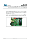
1
UM1604
User manual
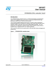
STEVAL-IHM039V1 dual motor control demonstration board
featuring the STM32F415 microcontroller
Introduction
The STEVAL-IHM039V1 demonstration board is designed as a dual motor field-oriented
control (FOC) development platform for STMicroelectronics' ARM Cortex™-M4 32-bit corebased STM32F415ZG microcontroller with up to 168 MHz of clock frequency and FPU
support. The board features full-speed USB 2.0 and CAN 2.0 A/B compliant interfaces; 1
I2S/I2C channel, 1 USART channel and 1 insulate USART through USB to serial bridge, 2
DAC channels, internal 192+4KB SRAM and 1 MB Flash memory, and JTAG and SWD
debugging support. The board is designed to implement multiple motor controls and offers
an advanced user I/O interface (LCD QVGA display and joystick key). Extension headers
make it easy to connect a daughterboard or wrapping board for specific applications.
With dedicated hardware features, the STEVAL-IHM39V1 board is designed to help
developers to evaluate the device and develop their own applications.
The STEVAL-IHM39V1 can be used together with the STM32 PMSM single/dual FOC SDK
v3.x and two of the possible STMicroelectronics demonstration power boards equipped with
MC connector for a complete dual motor control evaluation and development platform.
The demonstration board can be ordered through order code STEVAL-IHM039V1.
Figure 1. Demonstration board
March 2013
DocID024194 Rev 1
1/24
www.st.com
Contents
UM1604
Contents
1
Features . . . . . . . . . . . . . . . . . . . . . . . . . . . . . . . . . . . . . . . . . . . . . . . . . . . 3
2
Board description . . . . . . . . . . . . . . . . . . . . . . . . . . . . . . . . . . . . . . . . . . . 4
3
Jumper settings . . . . . . . . . . . . . . . . . . . . . . . . . . . . . . . . . . . . . . . . . . . . 13
4
Using the STEVAL-IHM039V1 with the STM32 FOC firmware library . 16
4.1
Hardware requirements . . . . . . . . . . . . . . . . . . . . . . . . . . . . . . . . . . . . . . 16
4.2
Software requirements . . . . . . . . . . . . . . . . . . . . . . . . . . . . . . . . . . . . . . . 16
5
Bill of material . . . . . . . . . . . . . . . . . . . . . . . . . . . . . . . . . . . . . . . . . . . . . 18
6
Revision history . . . . . . . . . . . . . . . . . . . . . . . . . . . . . . . . . . . . . . . . . . . 23
2/24
DocID024194 Rev 1
UM1604
1
Features
Features
•
STMicroelectronics’ ARMTM Cortex-M4 core-based STM32F415ZG microcontroller
•
Two full-featured MC connectors for interfacing with any of the possible
STMicroelectronics demonstration power boards
•
JTAG, SWD and trace debug support
•
USB connector for isolated virtual com port
•
USB 2.0 full speed connection
•
240 x 320 TFT color LCD
•
Joystick with 4-direction control and selector
•
4 LEDs
•
Reset plus three user buttons
•
Five 5 V power supply sources: 2-way screw connector, power jack, two USB
connectors or daughterboard
•
Boot from user Flash or system memory
•
CAN 2.0 A/B compliant connection
•
I2C connection
•
RS-232 channel with RTS/CTS handshake support
•
Extension connectors for daughterboard or wrapping area board
DocID024194 Rev 1
3/24
Board description
2
UM1604
Board description
Figure 2. Schematic diagram (1 of 9)
3*>@
3)>@
3(>@
3'>@
3&>@
3%>@
3$>@
3*>@
3)>@
3(>@
3'>@
3&>@
3%>@
3$>@
&21
5(6(7
3*
3*
3*
3&
3'
3'
3'
5
5
'9
3%
3%
3(
3(
3(
3'
3(
3(
3*
3)
3)
3%
3%
3%
3&
3$
3$
3$
3&
3&
3)
9
3*
3*
3*
3*
3'
3'
3'
3%
3%
3%
3%
3(
3(
3'
3(
3(
3*
3)
3)
3)
3&
3$
3$
3$
3$
3&
3&
+HDGHU[
&21
3&
3&
3$
3$
3$
3$
3&
3'
3(
3'
3'
3'
3'
3*
3*
3*
3%
3%
3%
3(
3(
3(
3&
3)
'9
- 3
3)
3)
3)
3)
9
+HDGHU[
4/24
DocID024194 Rev 1
3&
3&
3$
3$
3$
3$
3$
3&
3&
3'
3(
3'
3'
3*
3*
3*
3*
3%
3%
3%
3%
9
3(
3(
3&
- 3
3&
3)
3)
3)
3)
3)
UM1604
Board description
Figure 3. Schematic diagram (2 of 9)
9
5
N 5
5
8VHUB%XWWRQB
5
5
9
&
Q)
8 6(5 5
.
5
.
5
.
5 .
5
.
6: 5 5 5
8
5
-2<B6HOHFW
5 5
-2<B'RZQ
5 5
-2<B/HIW
5 5
-2<B5LJKW
5 5
-2<B8S
&
Q)
&
&
Q) Q)
&20021
6HOHFWLRQ
9
5 '2:1
/()7
+PZTUJDL
5
5,*+7
83
6: &
GRQRWILW
0 7 $
&
Q)
&
Q)
8 6(5 5 8VHUB%XWWRQB
5
5 .
9
&21
/&'B&6
/&'B6&/
/&'B6',
/&'B56
/&'B: 5
/&'B6'2
5(6(7
5 . &6
6&/
6',
56
:5
5'
6'2
5(6(7
5 8VHUB%XWWRQB
5
9
9
5 /&'%/B&RQWURO
5
5 GRQRWILW
9''
9&,
*1'
*1'
%/B9''
%/B&RQWURO
%/B*1'
%/B*1'
&
Q)
8 6(5 5 6: 5
&RORU/&'0RGXOH
DocID024194 Rev 1
5/24
Board description
UM1604
Figure 4. Schematic diagram (3 of 9)
9
5 .
5 .
5 .
5 .
- 3
%FGBVMUTFUUJOH0QFO
-7066: ',2
-7&.6: &/.
-7'2
-7',
-7567
5(6(7
9
&21
5 .
9
&21
5 GRQRWILW
5 GRQRWILW
- 7$ *
75 $ & (
5 5
5 5
75$&(B'
75$&(B'
75$&(B'
75$&(B'
75$&(B&.
6/24
DocID024194 Rev 1
9
5 GRQRWILW
5 N
5 N
5 N
DocID024194 Rev 1
0&B0DLQ&XUUHQW&
0&B0DLQ&XUUHQW%
5 5
Q)
& 5
5 5
& GRQRWILW
5 & GRQRWILW
0&B0DLQ3)&6\QF
0&B0DLQ&XUUHQW$
0&B0DLQ(PHUJHQF\6WRS
5
5 & Q)
5 .
%FGBVMU
TFUUJOH0QFO
0&B0DLQ3)&B3: 0
0&B0DLQ6SHHG6HQVRU$
0&B0DLQ6SHHG6HQVRU%
0&B0DLQ17&%\SDVVUHOD\
0&B0DLQ'LVVLSEUDNH
0&B0DLQ3: 0B8+
0&B0DLQ3: 0B8/
0&B0DLQ3: 0B9+
0&B0DLQ3: 0B9/
0&B0DLQ3: 0B: +
0&B0DLQ3: 0B: /
9
Q)
& - 3
- 8 0 3(5
9
& GRQRWILW
GRQRWILW
& 0&B0DLQFRQQHFWRU
&21
1'$0$1@4FOTF
&.&3(&/$:4501
.$@6)
(/%
.$@6(/%
.$@7)
(/%
.$@7(/%
.$@8)
(/%
#6470-5"(&
.$@8 $633&/5"
(/%
$633&/5#
(/%
$633&/5$
(/%
/5$#:1"443&-":
1'$7BD@TFOTF
%*44*1"5*7",& 1'$*BD@TFOTF
7108&3 )FBUTJOL5FNQFSBUVSF
1'$4:/$
71PXFS
1'$18.
(/%
&/$0%&3"
(/%
&/$0%&3#
&ODPEFS*OEFY
.PUPSDPOUSPMDPOOFDUP
S
& Q)
& Q)
& 0&B0DLQ+HDWVLQN7HPS
GRQRWILW
5
5 &
Q)
.
5 5
5 0&B0DLQ6SHHG6HQVRU&
5 5
& GRQRWILW
9
5 .
5 GRQRWILW
5 GRQRWILW
5 .
0&B0DLQ3)&B,DF
0&B0DLQ3)&B9DF
0&B0DLQ%XV9ROWDJH
0&B0DLQ3)&B2&3
UM1604
Board description
Figure 5. Schematic diagram (4 of 9)
7/24
8/24
DocID024194 Rev 1
0&B6XE&XUUHQW&
0&B6XE&XUUHQW%
0&B6XE&XUUHQW$
0&B6XE(PHUJHQF\6WRS
5 & GRQRWILW
5
5 5
& GRQRWILW
5 & GRQRWILW
5
5
5 & Q)
5 .
9
%FGBVMUTFUUJOH0QFO
0&B6XE6SHHG6HQVRU$
0&B6XE6SHHG6HQVRU%
0&B6XE17&%\SDVVUHOD\
0&B6XE'LVVLSEUDNH
0&B6XE3: 0B8+
0&B6XE3: 0B8/
0&B6XE3: 0B9+
0&B6XE3: 0B9/
0&B6XE3: 0B: +
0&B6XE3: 0B: /
9
Q )
& - 3
& GRQRWILW
& GRQRWILW
0&B6XEFRQQHFWRU
&.&3(&/$:4501
(/%
.$@6)
(/%
(/%
.$@6
(/%
.$@7)
.$@7(/%
.$@8)
(/%
.$@8#6470-5"(&
$633&/5"
(/%
$633&/5#
(/%
(/%
$633&/5$
1'$7BD@TFOTF
/5$#:1"443&-": 1'$*BD@TFOTF
%*44*1"5*7",&
)FBUTJOL5FNQFSBUVSF
7108&3
71PXFS
1'$4:/$
(/%
1'$18.
(/%
&/$0%&3"
&ODPEFS*OEFY
&/$0%&3#
&21
9
& 5
& GRQRWILW
Q)
5 5
5 7,0B&+
7,0B&+
7,0B&+
7,0B&+
7,0B&+
7,0B&+
0&B6XE6SHHG6HQVRU$
%FGBVMUCFUXFFOBOE
0&B6XE6SHHG6HQVRU%
%FGBVMUCFUXFFOBOE
0&B6XE+HDWVLQN7HPS
0&B6XE6SHHG6HQVRU&
& Q)
0&B6XE%XV9ROWDJH
0&B6XE6SHHG6HQVRU&
%FGBVMUCFUXFFOBOE
5 .
- 0 3
- 0 3
- 0 3 Board description
UM1604
Figure 6. Schematic diagram (5 of 9)
UM1604
Board description
Figure 7. Schematic diagram (6 of 9)
9
- 0 3
5 .
9
5
5 %FGBVMUTFUUJOH
& %FGBVMUTFUUJOH0QFO
Q)
- 3
- 8 0 3(5
8
&$1B7;
5 &$1B5;
% %
(/%
7$$
3 3
5
34
$"/)
$"/
7SFG
3
/
5 5
'%PDOHFRQQHFWRU
5 GRQRWILW
5 5
&$1
9
9
& Q)
5 GRQRWILW
& Q)
& Q)
8
86$57B7;
86$57B5;
86$57B576
86$57B&76
9
&
&
7LQ
5RXW
7LQ
5RXW
9
9&&
&
&
7RXW
5LQ
7RXW
5LQ
*1'
3
& Q) 5 5
5 5
'%PDOHFRQQHFWRU
6 7 ( % 7 5
& Q)
86$57
'
5HG
5 /('
5
-
,&B6'$
,&B60%$
/('
,&B6&/
2UDQJH
'
*UHHQ
'
%OXH
5
5 /('
5
,&
,&
'
5 5 /('
5
/('
9
5 5 9
.
3RWHQWLRPHWHU
5
& Q)
3RWHQWLRPHWHU
DocID024194 Rev 1
9/24
$X['&
' & %
8 = ( 1 9 $ /6
,1
287
*1'
DocID024194 Rev 1
5 & 5
X)
95()
& 2 1 & X)
89
-
& Q)
9%$7
95()
9''$
9''B
9''B
9''B
9''B
9''B
9''B
9''B
9''B
9''B
9''B
9''B
6 7 0 ) = * 7 9''B
95()
9&$3
9&$3
966B
3'5B21
966B
966B
966B
966B
966B
966B
966B
966B
8 %
5,'&'&FRQYHUWHU
34DPEF
4*1
6 0 $ - $ 7 5
=
9''
& X)
9''$
5 5
9''$
- 3 - 3 - 3 - 3
& X) Y
/
%($'GLVWUHOHF
%FGBVMU+1QSFTFOU
- 3 & Q)
9
95()
Q)
& (9
9
Q )
& Q )
& 5
5 '
Q)
& & X) 9
9
%FGBVMUTFUUJOHKVNQFSQSFTFOUPOMZPO+1QJOT
86%9
(9
&*
&*
&*
&9
% 1 ; 6*
69
'9
8
8
Q)
& 9''
5HG
9,1
& Q)
Q)
& 9287
/' ' 0 *1'
10/24
& 2 1 & Q)
& X)
& Q)
Q)
& & Q)
9
Q)
& 9''
& Q)
& Q)
Board description
UM1604
Figure 8. Schematic diagram (7 of 9)
7,0B&+
& 2 1 B
- 3
- 0 3
0&B6XE%XV9ROWDJH
0&B0DLQ3)&B9DF
7,0B&+
0&B0DLQ3)&B3: 0
-7567
0&B0DLQ3)&6\QF
9
0&B0DLQ+HDWVLQN7HPS
7,0B&+
0&B6XE&XUUHQW&
0&B6XE+HDWVLQN7HPS
0&B0DLQ3)&B,DF
-7'2
86$57B7;
86$57B5;
86%'0
86%'3
-7066: ',2
-7&.6: &/.
-7',
DocID024194 Rev 1
S)
& S )
& 6
9
& S)
5
5 <
0 + ]
5 .
Q)
& 5 (6(7
5(6(7
. K]
<
9
5 5 5 5 /&'B6&/
/&'B6'2
/&'B6',
0&B6XE&XUUHQW$
0&B0DLQ%XV9ROWDJH
0&B6XE3: 0B8+
0&B6XE3: 0B9+
0&B6XE3: 0B: +
0&B0DLQ&XUUHQW$
0&B0DLQ&XUUHQW%
0&B0DLQ&XUUHQW&
0&B6XE3: 0B9/
0&B6XE3: 0B: /
0&B0DLQ'LVVLSEUDNH
0&B0DLQ17&%\SDVVUHOD\
0&B6XE'LVVLSEUDNH
0&B6XE17&%\SDVVUHOD\
0&B0DLQ6SHHG6HQVRU&
& S )
5 .
0&B6XE&XUUHQW%
0&B6XE(PHUJHQF\6WRS
0&B6XE3: 0B8/
/&'B&6
- 0 3
- 0 3
- 0 3
6: %2 2 7
- 0 3
0&B0DLQ6SHHG6HQVRU$
0&B0DLQ6SHHG6HQVRU%
5 .
8 $
6 7 0 ) = * 7 %227
26&B,1
26&B287
1567
3&$'&B,1
3&$'&B,1
3&$'&B,1
3&$'&B,1
3&$'&B,1
3&$'&B,1
3&7,0B&+
3&7,0B&+
3&7,0B&+
3&7,0B&+
3&63,B6&.
3&63,B026,
3&63,B0,62
3&$17,7$03
3&26&,1
3&26&287
3%7,0B&+$'&B&KDQQHOB
3%7,0B&+$'&B&KDQQHOB
3%%227
3%-7'26:'B6:27,0B&+63,B6&.
3%-75677,0B&+63,B0,62
3%7,0B&+63,B026,
3%,&B6&/
3%,&B6'$
3%
3%
3%7,0B&+
3%7,0B&+
3%63,B166
3%63,B6&.
3%63,B0,627,0B&+1
3%63,B026,7,0B&+1
3$:.837,0B&+7,0B&+
3$7,0B&+7,0B&+
3$7,0B&+$'&B&KDQQHOB
3$$'&B,1
3$$'&B,1'$&B287
3$$'&B,1'$&B287
3$7,0B%.,1
3$7,0B&+1
3$
3$86$57B7;
3$86$57B5;
3$86%'0
3$86%'3
3$-7066:',2
3$-7&.6:&/.
3$-7',7,0B&+B(7563,B166
% 2 2 7
6: 26&B,1
26&B287 5(6(7
3&
3&
3&
3&
3&
3&
3&
3&
3&
3&
3&
3&
3&
3&
3&
3%
3%
3%
3%
3%
3%
3%
3%
3%
3%
3%
3%
3$
3$
3$
3$
3$
3$
3$
3$
3$
3$
3$
3$
3$
3$
3$
3$
3'7,0B&+
3'7,0B&+
3'7,0B&+
3'7,0B&+
3'
3'
3'
3'
3'
3'86$57B5;
3'86$57B7;
3'86$57B576
3'86$57B&76
3'7,0B(75
3'&$1B7;
3'&$1B5;
3(7,0B%.,1
3(
3(7,0B&+
3(7,0B&+1
3(7,0B&+
3(7,0B&+1
3(7,0B&+
3(7,0B&+1
3(
3(
3(
3(
3(
3(
3(
3(7,0B(75
3)
3)
3)
3)
3)
3)$'&B,1
3)$'&B,1
3)$'&B,1
3)$'&B,1
3)$'&B,1
3)
3)
3)
3),&B60%$
3),&B6&/
3),&B6'$
3*
3*
3*
3*
3*
3*
3*
3*
3*
3*
3*
3*
3*
3*
3*
3*
3'
3'
3'
3'
3'
3'
3'
3'
3'
3'
3'
3'
3'
3'
3'
3'
3(
3(
3(
3(
3(
3(
3(
3(
3(
3(
3(
3(
3(
3(
3(
3(
3)
3)
3)
3)
3)
3)
3)
3)
3)
3)
3)
3)
3)
3)
3)
3)
3*
3*
3*
3*
3*
3*
3*
3*
3*
3*
3*
3*
3*
3*
3*
3*
- 3
- 8 0 3(5
/&'B56
86$57B5;
86$57B7;
86$57B576
86$57B&76
0&B0DLQ3)&B2&3
&$1B7;
&$1B5;
7,0B&+
7,0B&+
7,0B&+
/&'B: 5
/('
/('
/('
/('
0&B0DLQ3: 0B: +
0&B0DLQ3: 0B: /
0&B0DLQ3: 0B9+
0&B0DLQ3: 0B9/
0&B0DLQ3: 0B8+
0&B0DLQ3: 0B8/
0&B0DLQ(PHUJHQF\6WRS
,&B60%$
,&B6&/
,&B6'$
3RWHQWLRPHWHU
8VHUB%XWWRQB
8VHUB%XWWRQB
8VHUB%XWWRQB
-2<B6HOHFW
-2<B'RZQ
-2<B/HIW
-2<B5LJKW
-2<B8S
34
0LQL86%W\SH%FRQQ
9&&
'
'
1&
*1'
6+
6+
6+
6+
& 2 1 86%9
3$
3$
3$
3$
3$
3$
3$
3$
3$
3$
3$
3$
3$
3$
3$
3$
3(
3(
3(
3(
3(
3(
3(
3(
3(
3(
3(
3(
3(
3(
3(
3(
N
5
5
5 5 5 3$>@
3%
3%
3%
3%
3%
3%
3%
3%
3%
3%
3%
3%
3%
3%
3%
3%
3(>@
3)
3)
3)
3)
3)
3)
3)
3)
3)
3)
3)
3)
3)
3)
3)
3)
86%'3
86%'0
3$>@
3%>@
3&
3&
3&
3&
3&
3&
3&
3&
3&
3&
3&
3&
3&
3&
3&
3&
3(>@
3)>@
3*
3*
3*
3*
3*
3*
3*
3*
3*
3*
3*
3*
3*
3*
3*
3*
5 N
5 N
3%>@
3&>@
3'
3'
3'
3'
3'
3'
3'
3'
3'
3'
3'
3'
3'
3'
3'
3'
3)>@
3*>@
4
6 7 5 9
3&>@
3'>@
3*>@
3'>@
UM1604
Board description
Figure 9. Schematic diagram (8 of 9)
11/24
12/24
DocID024194 Rev 1
7JSUVBM$0.
*OTVMBUFE
86%W\SH%FRQQ
&
Q)
'
'
05
5
&
X)
89
'
'
.
*0
7CVT *0 8
Q)
&
89
675
4
.
5
N
86%B'0
86%B'3
86%B'LVFRQQHFW
- 03 &
Q)
89
9''
966
3$
3$
3$
3$
3$
3$
3&
3&
3&
3&
3%
3%
3%
3%
'MBTI
4ZTUFN
89
%FGBVMUTFUUJOH
5 5
89 & Q)
5 5
#005
5
.
89
86%/&6&
*0
(/%
*0
86%B'LVFRQQHFW
5
675
4
.
89
5
5
89
&
Q)
9%$7
3&7$0357&
3&
3&
3'26&,1
3'26&287
1567
3&
3&
3&
3&
966$
9''$
3$:.83
3$
3$
7$$
%
%
(/%
4)&-4)&--
89
S)
8
%227
6: 9''
966
3%
3%
3%
3%
3%
3&
3&
3$
3$
3$
3$
9''$
966$
3$
&21
&
Q)
5
89
670)57
8B6:&/.
5 N
3$
3$
3&
3&
3&
3'
3%
3%
3%
3%
3%
%227
3%
3%
966
9''
86%5HVHW
%
;
0+]
&
S)
&
&
Q)
8B6:',2
8B6:&/.
-
89
X)9
&
89
9''
*1'
,1
,1
287
287
1&
*1'
8
,1+
,1
*1'
287
-
9''
*1'
287
287
,1
,1
1&
*1'
9
X)9
&
89
,/(
SLQ62,&
/'$%075627/
8B86$57B5;
89
8B6:',2
86%B'3
86%B'0
8B86$57B5;
8B86$57B7;
89
8B86$57B7;
&
Q)
86$57B5;
89
'
*UHHQ
5
N
86$57B7;
Board description
UM1604
Figure 10. Schematic diagram (9 of 9)
UM1604
3
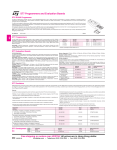
Jumper settings
Jumper settings
Table 1 gives a detailed description of the jumpers used.
Table 1. Jumper settings
Jumper
Selection
Close
PC14 is connected to the
extension connector CON3
Open (default)
PC14 isn't connected to the
extension connector CON3
Close
PC15 is connected to the
extension connector CON3
Open (default)
PC15 isn't connected to the
extension connector CON3
Close
Add 10nF of capacitor to filter
the motor 1 sensor input
(Encoder A/H1)
Open (default)
No filter added
Close
Add 10nF of capacitor to filter
the motor 2 sensor input
(Encoder A/H1)
Open (default)
No filter added
Between 1-2 (default)
TIM4_CH3 is used for motor 2
sensor input (Encoder
Index/H3)
Between 2-3
TIM3_CH3 is used for motor 2
sensor input (Encoder
Index/H3). See JMP5.
Between 1-2 (default)
TIM4_CH2 is used for motor 2
sensor input (Encoder B/H2)
Between 2-3
TIM3_CH2 is used for motor 2
sensor input (Encoder B/H2).
See JPM8.
Between 1-2 (default)
TIM4_CH1 is used for motor 2
sensor input (Encoder A/H1)
Between 2-3
TIM3_CH1 is used for motor 2
sensor input See JP5.
Open
+5 V is not supplied by the 2way screw connector CON13 or
by the power jack CON12
Close (default)
+5 V is supplied by the 2-way
screw connector CON13 or by
the power jack CON12
JP1
JP2
JP4
JP6
Description
JMP3
JMP4
JMP10
JP9
DocID024194 Rev 1
13/24
Jumper settings
UM1604
Table 1. Jumper settings (continued)
Jumper
Selection
Open (default)
+5 V is not connected to the
extension connector
Close
+5 V is connected to the
extension connector
Open (default)
+5 V is not supplied by USB
connector CON11
Close
+5 V is supplied by USB
connector CON11
Open (default)
+5 V is not supplied by USB
connector CON14
Close
+5V is supplied by USB
connector CON14
Between 1-2
The microcontroller pin PB0
(TIM3_CH3) is used for motor 2
sensor input (Encoder
Index/H3). See JMP3.
Between 2-3 (default)
The microcontroller pin PB0
(ADC12_IN8) is connected to
the phase C motor 2 current
feedback (MC_Sub1 CurrentC).
Between 1-2
Use this setting if TIM3 is used
for speed and positioning
feedback for the motor 2.
Between 2-3 (default)
The microcontroller pin PB1
(ADC12_IN9) is connected to
the temperature sensor of
power stage 1 (MC_Main
Heatsink Temp).
Between 1-2 (default)
The microcontroller pin PA2
(ADC123_IN2) is connected to
the temperature sensor of
power stage 2 (MC_Sub1
Heatsink Temp).
Between 2-3
The microcontroller pin PA2
(ADC123_IN2) is connected to
the AC current feedback of
power stage 1 (MC_Main
PFC_Iac).
Between 1-2
The microcontroller pin PB5
(TIM3_Ch2) is used for motor
control 2 sensor input (Encoder
B/H2). See JPM4.
Between 2-3
The microcontroller pin PB5
(TIM3_Ch2) is connected to the
PFC PWM output (MC_Main
PFC_PWM).
JP10
JP11
JP13
JMP5
JMP6
JMP7
JMP8
14/24
Description
DocID024194 Rev 1
UM1604
Jumper settings
Table 1. Jumper settings (continued)
Jumper
Selection
Between 1-2
The microcontroller pin PC3
(ADC123_IN13) is connected to
the AC voltage input sensing of
the power stage 1 (MC_Main
PFC_Vac).
Between 2-3 (default)
The microcontroller pin PC3
(ADC123_IN13) is used for bus
voltage measurement of the
power stage 2 (MC_Sub1 Bus
Voltage).
Between 1-2 (default)
The microcontroller pin PB4
(JTRST) is connected to the
JTAG connector CON6
Between 2-3
The microcontroller pin PB4 is
connected to the
synchronization feedback signal
coming from power stage
(MC_Main PFC Sync)
Between 2-4
The microcontroller pin PB4
(TIM3_CH1) is used for motor
control 2 sensor input (Encoder
A/H1). See JMP10.
Closed
This must be closed if TIM4 is
used for speed and positioning
feedback for the motor 2.
JMP9
JP5
JP7
Description
DocID024194 Rev 1
15/24
Using the STEVAL-IHM039V1 with the STM32 FOC firmware library
4
UM1604
Using the STEVAL-IHM039V1 with the STM32 FOC
firmware library
The “STM32 FOC firmware library” provided together with the STM3210B-MCKIT performs
the field oriented control (FOC) of a permanent magnet synchronous motor (PMSM) in both
sensor and sensorless configurations.
It is possible to configure the firmware to work with the STEVAL-IHM039V1 board and to
establish a real-time communication for debugging/tuning purposes using the ST motor
control workbench.
This section describes how the “STM32 FOC firmware library” v3.2 or higher can be used
together with the STEVAL-IFN003V1 and with the ST motor control workbench release 2.0
or higher.
4.1
Hardware requirements
The following items are required to run the STEVAL-IHM039V1 together with the “STM32
FOC firmware library”.
4.2
•
The STEVAL-IHM039V1 board
•
A DC power supply (up to 48 V)
•
A programmer/debugger dongle (not included in the package). To program/debug the
STEVAL-IHM039V1, a dongle with JTAG or single wire debugging capabilities (SWD)
is required. Use of an insulated dongle (like “ST-LINK/V2-ISOL”) is always
recommended.
•
A 3-phase brushless motor with permanent magnet rotor (not included in the package)
•
A USB cable with USB connector (type B) to establish a real-time communication (not
included in the package).
•
An insulated oscilloscope (as needed).
•
An insulated multimeter (as needed).
Software requirements
To customize, compile and download the “STM32 FOC firmware library” v3.2 or above, a
tool chain must be installed. Please refer to the UM1052 user manual for details on how to
set up the proper tool chain.
Before establishing the real-time communication it is also necessary to install the “STM32
Virtual COM Port Driver” available for download from the ST website.
Two specific configuration files for the ST motor control Workbench designed to work with
the STEVAL-IHM039V1 exist (see Table 2). Both are present in the STM32 PMSM FOC
Firmware Library, under “\Utilities\WB_Projects\SDK3xx” subfolder or in the ST MC
Workbench, under “\WB_Projects\SDK3xx”.
16/24
DocID024194 Rev 1
UM1604
Using the STEVAL-IHM039V1 with the STM32 FOC firmware library
Table 2. STEVAL-IHM039V1 configuration files for ST motor control Workbench
Configuration file name
SDK3xx-STEVAL-IHM039V1-MB459-Shinano-SINGLE-DRIVE.stmc
SDK32x-STEVAL-IHM039V1-MB459-Shinano-DUAL-DRIVE.stmc
Intended use
STEVAL-IHM039 in single
drive configuration
STEVAL-IHM039 in dual
drive configuration
To establish real-time communication between STEVAL-IHM039V1 and the ST motor
control Workbench, after installing the “STM32 Virtual COM Port Driver”, connect a USB
cable (type B) to the CON11 connector on the STEVAL-IHM039V1.
New hardware will be found on the system and the driver will be installed. A new COM port
will be added to the system and the new COM port (Ex. COM58) can be set up in the ST
motor control Workbench under the “monitor” window to establish the connection.
DocID024194 Rev 1
17/24
Bill of material
5
UM1604
Bill of material
Table 3. Bill of material
Item
Quantity
1
1
2
3
2
1
Reference
Part
B1
CON1,CON3
CON4
Tolerance
Description
TD-0341
[RESET/Black]
Micro tactile switch
Header 35 x 2
2x35 way double row
strip line connector
(male connector)
2.54 mm pitch
Color LCD module
2 strip line connector
(female connector) 2x8
way double row
2.54 mm pitch
4
1
CON5
TRACE
2x10 way double row
strip line connector
(male connector)
1.27 mm pitch
5
1
CON6
JTAG
20 way IDC low profile
boxed header 2.54 mm
pitch
6
1
CON8
MC_Main connector
34 way IDC low profile
boxed header 2.54 mm
pitch
7
1
CON9
MC_Sub1 connector
34 way IDC low profile
boxed header 2.54 mm
pitch
8
1
CON11
USB-typeB conn.
USB connector
9
1
CON12
DC-10B
Mini DC power socket
2.5 mm
10
1
CON13
Aux DC - 250 V
2 way PCB screw
terminal, 5.08 mm pitch
11
1
CON14
MiniUSB-typeB conn.
MiniUSB connector
12
40
C1,C3,C4,C5,C6,C7,C
8,C9,
100 nF 16 V
13
C15,C20,C23,C26,C28,
C34,C35,
14
C36,C37,C38,C39,C40,
C42,C44,
15
C45,C46,C47,C50,C57,
C60,C61,
16
C62,C63,C64,C65,C66,
C67,C68,
17
C69,C70,C74,C75
18/24
DocID024194 Rev 1
+/-10%
Ceramic capacitor X7R
UM1604
Bill of material
Table 3. Bill of material (continued)
Item
Quantity
Reference
Part
18
21
C2,C12,C13,C14,C17,
C18,
19
C19,R24,C25,C27,C29,
R30,
20
C30,R31,C31,R32,C32,
R44,
21
R47,R61,R83
Tolerance
Description
do not fit
22
2
C10,C24
1 nF
+/-10%
Ceramic capacitor X7R
23
1
C11
22 nF
+/-10%
Ceramic capacitor X7R
24
4
C16,C21,C33,C54
10 nF
+/-10%
Ceramic capacitor X7R
25
1
C22
1 uF
+/-10%
Ceramic capacitor X7R
26
4
C41,C58,C59,C73
22 pF
+/-10%
Ceramic capacitor X7R
27
1
C43
4.7 nF
+/-10%
Ceramic capacitor X7R
28
1
C48
10 uF 16 V
+/-10%
Electrolytic aluminum
capacitor
29
1
C49
470 uF 10 V
+/-10%
Electrolytic aluminum
capacitor
30
2
C51,C53
10 uF
+/-10%
Ceramic capacitor X7R
31
1
C52
470 nF
+/-10%
Ceramic capacitor X7R
32
2
C55,C56
10 pF
+/-10%
Ceramic capacitor X7R
33
1
C71
1 uF
+/-10%
Ceramic capacitor X7R
34
1
C72
2.2 uF 10 V
+/-20%
Electrolytic aluminum
capacitor
35
2
C76,C77
2.2 uF 16 V
+/-10%
Ceramic capacitor X7R
36
2
D1,D5
Red
Chip LED
37
1
D2
Orange
Chip LED
38
2
D3,D6
Green
Chip LED
39
1
D4
Blue
Chip LED
10
JMP1,JMP2,JMP3,JMP
Jump_linear 3
4,JMP5,
40
41
JMP6,JMP7,JMP8,JMP
9,
42
JMP10
43
JP1,JP2,JP3,JP4,JP6,J
JUMPER
P7,JP8,JP9,
11
DocID024194 Rev 1
3 way single row strip
line connector (male
connector) 2.54mm
pitch
2 way single row strip
line connector (male
connector) 2.54mm
pitch
19/24
Bill of material
UM1604
Table 3. Bill of material (continued)
Item
Quantity
44
45
Reference
Part
Tolerance
Description
JP10,JP11,JP12
1
JP5
CON3+1_1
3+1 way single row
strip line connector
(male connector)
2.54mm pitch
46
1
J1
I2C
4 way single row strip
line connector (male
connector) 2.54mm
pitch
47
1
J2
RI-0505 DC-DC
converter
Isolated DC-DC
converter
48
1
J3
IL516-3E 0.15'' 16-pin
SOIC
4 channel opto-isolator
49
1
J4
50
1
L1
BEAD distrelec 330005
Data line filter
51
2
P1,P2
DB9-male connector
9 way r/a PCB D
plug,US footprint
52
3
Q1,Q2,Q3
2STR1215
Low voltage fastswitching NPN power
transistor
53
22
R6,R7,R8,R9,R10,R25, 10 K
3 way dual row strip line
connector
(male
connector)
2,54 mm
pitch
54
R26,R27,R28,R29,R33,
R34,
55
R35,R63,R64,R73,R77,
R88,
56
R91,R92,R97
+/- 1%
Resistor
57
2
R1,R2
820
+/- 1%
Resistor
58
2
R3,R20
4K7
+/- 1%
Resistor
59
4
R4,R11,R16,R23
100 R
+/- 1%
Resistor
60
32
R5,R12,R13,R14,R15,
R17,
0R
+/- 1%
Resistor
61
R21,R22,R36,R37,R40,
R41,
62
R45,R46,R48,R49,R50,
R52,
63
R53,R54,R56,R57,R58,
R59,
20/24
DocID024194 Rev 1
UM1604
Bill of material
Table 3. Bill of material (continued)
Item
Quantity
Reference
Part
64
R60,R76,R78,R80,R84,
R87,
65
R89,R90
Tolerance
Description
66
1
R18
330 R
+/- 1%
Resistor
67
1
R19
220 K
+/- 1%
Resistor
68
2
R38,R51
3.3 K
+/- 1%
Resistor
69
3
R39,R42,R55
100 K
+/- 1%
Resistor
70
1
R43
4.7 K
+/- 1%
Resistor
71
1
R62
1k
+/- 1%
Resistor
72
4
R65,R66,R69,R71
600 R
+/- 1%
Resistor
73
2
R67,R68
22 R
+/- 1%
Resistor
74
1
R70
1 MR
+/- 1%
Resistor
75
2
R72,R96
1.5 K
+/- 1%
Resistor
76
2
R74,R98
36 K
+/- 1%
Resistor
77
1
R75
47 K
+/- 1%
Resistor
78
1
R79
220
+/- 1%
Resistor
79
1
R82
120 R
+/- 1%
Resistor
80
1
R85
300 R
+/- 1%
Resistor
81
1
R86
47 R
+/- 1%
Resistor
82
1
R93
390 R
+/- 1%
Resistor
83
2
R94,R95
10 R
+/- 1%
Resistor
84
1
SW1
USER3
Surface mount tactile
switch
85
1
SW2
USER2
Surface mount tactile
switch
86
1
SW3
USER1
Surface mount tactile
switch
87
1
SW4
BOOT1
1-pole miniature slide
switches through hole
88
2
SW5,SW6
BOOT0
1-pole miniature slide
switches through hole
89
1
S1
RESET
Surface Mount Tactile
Switch
90
1
U1
MT008-A
Joystick
91
1
U2
USBLC6-2SC6
Very low capacitance
ESD protection
92
1
U3
L9615
CAN transceiver
93
1
U4
ST3232EBTR
RS-232 transceiver
DocID024194 Rev 1
21/24
Bill of material
UM1604
Table 3. Bill of material (continued)
Item
Quantity
94
1
U5
ZEN056V130A24LS
95
1
U6
BNX002-01
96
1
U7
LD1086D2M33TR
97
1
U8
STM32F415ZGT6
98
1
U9
STM32F103R8T6
99
1
U11
LD2981ABM33TR
100
2
X1,Y2
8 MHz
101
1
Y1
32.768 KHz
102
1
Z1
SMAJ5.0A-TR
103
1
RV1
10 K (Trimmer)
104
22/24
14
Reference
Part
Tolerance
5.6 V
50 V/10 A
Description
Polymer protected
Zener diode 5.6V
PCB mount DC power
filter
Low drop linear
regulator
Low drop linear
regulator
Transil
Jumper on
JMP3,JMP4,JMP10,JM
P5, JMP6,
JMP7,JMP8,JMP9,JMP
2,JP5,JMP1,JP7,JP9,J
P12
jumper
DocID024194 Rev 1
UM1604
6
Revision history
Revision history
Table 4. Document revision history
Date
Revision
19-Mar-2013
1
Changes
Initial release.
DocID024194 Rev 1
23/24
UM1604
Please Read Carefully:
Information in this document is provided solely in connection with ST products. STMicroelectronics NV and its subsidiaries (“ST”) reserve the
right to make changes, corrections, modifications or improvements, to this document, and the products and services described herein at any
time, without notice.
All ST products are sold pursuant to ST’s terms and conditions of sale.
Purchasers are solely responsible for the choice, selection and use of the ST products and services described herein, and ST assumes no
liability whatsoever relating to the choice, selection or use of the ST products and services described herein.
No license, express or implied, by estoppel or otherwise, to any intellectual property rights is granted under this document. If any part of this
document refers to any third party products or services it shall not be deemed a license grant by ST for the use of such third party products
or services, or any intellectual property contained therein or considered as a warranty covering the use in any manner whatsoever of such
third party products or services or any intellectual property contained therein.
UNLESS OTHERWISE SET FORTH IN ST’S TERMS AND CONDITIONS OF SALE ST DISCLAIMS ANY EXPRESS OR IMPLIED
WARRANTY WITH RESPECT TO THE USE AND/OR SALE OF ST PRODUCTS INCLUDING WITHOUT LIMITATION IMPLIED
WARRANTIES OF MERCHANTABILITY, FITNESS FOR A PARTICULAR PURPOSE (AND THEIR EQUIVALENTS UNDER THE LAWS
OF ANY JURISDICTION), OR INFRINGEMENT OF ANY PATENT, COPYRIGHT OR OTHER INTELLECTUAL PROPERTY RIGHT.
ST PRODUCTS ARE NOT AUTHORIZED FOR USE IN WEAPONS. NOR ARE ST PRODUCTS DESIGNED OR AUTHORIZED FOR USE
IN: (A) SAFETY CRITICAL APPLICATIONS SUCH AS LIFE SUPPORTING, ACTIVE IMPLANTED DEVICES OR SYSTEMS WITH
PRODUCT FUNCTIONAL SAFETY REQUIREMENTS; (B) AERONAUTIC APPLICATIONS; (C) AUTOMOTIVE APPLICATIONS OR
ENVIRONMENTS, AND/OR (D) AEROSPACE APPLICATIONS OR ENVIRONMENTS. WHERE ST PRODUCTS ARE NOT DESIGNED
FOR SUCH USE, THE PURCHASER SHALL USE PRODUCTS AT PURCHASER’S SOLE RISK, EVEN IF ST HAS BEEN INFORMED IN
WRITING OF SUCH USAGE, UNLESS A PRODUCT IS EXPRESSLY DESIGNATED BY ST AS BEING INTENDED FOR “AUTOMOTIVE,
AUTOMOTIVE SAFETY OR MEDICAL” INDUSTRY DOMAINS ACCORDING TO ST PRODUCT DESIGN SPECIFICATIONS.
PRODUCTS FORMALLY ESCC, QML OR JAN QUALIFIED ARE DEEMED SUITABLE FOR USE IN AEROSPACE BY THE
CORRESPONDING GOVERNMENTAL AGENCY.
Resale of ST products with provisions different from the statements and/or technical features set forth in this document shall immediately void
any warranty granted by ST for the ST product or service described herein and shall not create or extend in any manner whatsoever, any
liability of ST.
ST and the ST logo are trademarks or registered trademarks of ST in various countries.
Information in this document supersedes and replaces all information previously supplied.
The ST logo is a registered trademark of STMicroelectronics. All other names are the property of their respective owners.
© 2013 STMicroelectronics - All rights reserved
STMicroelectronics group of companies
Australia - Belgium - Brazil - Canada - China - Czech Republic - Finland - France - Germany - Hong Kong - India - Israel - Italy - Japan Malaysia - Malta - Morocco - Philippines - Singapore - Spain - Sweden - Switzerland - United Kingdom - United States of America
www.st.com
24/24
DocID024194 Rev 1