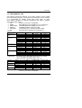
1
GA - 586HX USER'S MANUAL PCI - ISA SOLUTION PENTIUM PCI - ISA BUS MAINBOARD REV.2.0 Second Edition GA-586HX Who need 82430HX? 1. If you want to get the best performance. (Because more buffers & Quick DRAM Timing is supported.) 2. If your DATABASE is very imporant. (Because single bit error correction & Multi-bit error detection is supported.) 3. If you want to use memory more than 64MB. (Because 512MB memory size cacheable is supported.) 4. If you need more flexibility to upgrade your memory. (Because 4 banks DRAM is supported.) 5. If you need a USB ports for C&C application. (Because 2 USB ports will be ready in the end of Q2/96".) Why do you need GA-586HX 82430HX motherboard? 1. Because it is the best performance motherboard, see next page, we compare GA-586HX with PC Magazine EDITOR choice-system. 2. Because user can easily make you memory cacheable size to 512MB. Others can't, because they don't have an EXTRA TAG-RAM socket. 3. Because GA-586HX has 3 banks DRAM, you may upgrade your memory easily & with flexibility. Others don't, because they only have 2 banks 72-pin SIMM modules. 4. Just plug a 256KB Pipeline cache module, you can get cache size to 512KB easily, no jumper setting needed. Others don't, because they don't have an upgrade cache module, or they have to change jumper setting to 512KB. 5. No risk for Intel P55CT CPU upgrade because GA-586HX will auto detect P55CT, and support right operation voltage. Others don't, because they need an EXTRA VRM module or jumper setting for P55CT CPU upgrade. 6. DIP switch setting is supported, you don't have to worry any jumper shunter missed. Others don't, because they have jumpers on board. I. PERFORMANCE 2 Table of Contents Gateway P5-166 XL (P/166) / SAG STF 166(P/166): These two systems' score are according to PC Magazine February 20, 1996. Page 146-148. GA-586SVX (P166): The system tested with 1.2GB hard disk drive, 4 x CD-ROM, and 16MB of EDO RAM. Using each graphics driver provides from Windows95 1024 by 768 resolution with 256 colors, small font, and a refresh rate 72Hz, we defragmented hard disk before each test for Windows95 manage virtual memory setting. Hardware Configuration: • CPU Intel 166 MHz • RAM 8MB 2pcs. Total 16 MB (Panasonic EUXSR08XX00E) • Cache size 256 KB Pipeline Burst SRAM (UMC UM61L3232AF-7) 2 pcs. 512 KB Pipeline Burst SRAM (UMC UM61L3232AF-7) 4 pcs. • DISPLAY Matrox MGA Millennium Power Desk • STORAGE Quantum Fireball 1280AT • O.S. Windows 95 O.S. Cache size Gateway P5-166 XL(P/166) Windows95 256KB Matrox MGA Impression 75 SAG STF 166(P/166) Windows95 512KB Image 128#9 76 GA-586HX(P/166) Windows95 256KB Matrox MGA Millennium Power Desk 80.1 GA-586HX(P/166) Windows95 512KB Matrox MGA Millennium Power Desk 82.4 II. Quick Installation Guide: 3 VGA WINSTONE96 GA-586HX Intel CPU SW1 SW2 SW3 SW4 1. Pentium 75 MHz OFF OFF ON ON 2. Pentium 90 MHz OFF OFF OFF ON 3. Pentium 100 MHz OFF OFF ON OFF 4. Pentium 120 MHz ON OFF OFF ON 5. Pentium 133 MHz ON OFF ON OFF 6. Pentium 150 MHz/P55C-150MHz ON ON OFF ON 7. Pentium 166MHz ON ON ON OFF 8. Pentium 180 MHz OFF ON OFF ON 9. Pentium 200 MHz/P55C-200MHz OFF ON ON OFF 10. P54CT-125 MHz ON ON ON ON 11. P54CT-150 MHz ON ON OFF ON 12. P54CT-166 MHz ON ON ON OFF 166 MHz/P55C- 13. P54CTB-150 MHz ¬¬ ON ON OFF ON 14. P54CTB-166 MHz ¬¬ ON ON ON OFF 15. P54CTB-180 MHz ¬¬ OFF ON OFF ON 16. P54CTB-200 MHz ¬¬ OFF ON ON OFF 4 Table of Contents AMD/Cyrix CPU SW1 SW2 SW3 SW4 17. AMDK5- 75 MHz-P75 OFF OFF ON ON 18. AMDK5- 90 MHz-P90 OFF OFF OFF ON 19. AMDK5-100 MHz-P100 OFF OFF ON OFF 20. AMDK5- OFF OFF OFF ON 21. AMDK5-100 MHz-P133 ON OFF ON OFF 22. AMDK5-P166 ON ON ON OFF 23. AMDK5-P200 OFF ON ON OFF 24. Cyrix 6x86-100 MHz-P120+ ON OFF ON ON 25. Cyrix 6x86-110 MHz-P133+ ON OFF OFF OFF 26. Cyrix 6x86-120 MHz-P150+ ON OFF OFF ON 27. Cyrix 6x86-133 MHz-P166+ ON OFF ON OFF 28. Cyrix 6x86L- P150+ 2.8V ON OFF OFF ON 29. Cyrix 6x86L-P166+ 2.8V ON OFF ON OFF 90 MHz-P120 ¬ Note : If Cyrix 6x86 is being used, please check the CPU Date Code after 605. ¬¬ Note : To Support Intel CPU P54CTB-150MHz/166MHz/180MHz/200MHz, GA-586HX Is Available From PCB Ver.1.54. 5 GA-586HX 1. Pentium 75 MHz Pentium 75 MHz CPU OFF ON 1 2 3 4 SW 2. Pentium 90 MHz Pentium 90 MHz CPU OFF ON 1 2 3 4 SW 3. Pentium 100 MHz Pentium 100 MHz CPU OFF ON 1 2 3 4 SW 4. Pentium 120 MHz 6 Table of Contents Pentium 120 MHz CPU OFF ON 1 2 3 4 SW 5. Pentium 133 MHz Pentium 133 MHz CPU OFF ON 1 2 3 4 SW 6. Pentium 150 MHz/P55C-150MHz Pentium 150 MHz/P55C-150MHz CPU OFF ON 1 2 3 4 SW 7. Pentium 166 MHz/P55C-166MHz 7 GA-586HX Pentium 166 MHz/P55C-166MHz CPU OFF ON 1 2 3 4 SW 8. Pentium 180 MHz Pentium 180 MHz CPU OFF ON 1 2 3 4 SW 9. Pentium 200 MHz/P55C-200MHz Pentium 200 MHz/P55C-200MHz CPU OFF ON 1 2 3 4 SW 10. P54CT-125 MHz 8 Table of Contents P54CT-125 MHz CPU OFF ON 1 2 3 4 SW 11. P54CT-150 MHz P54CT-150 MHz CPU OFF ON 1 2 3 4 SW 12. P54CT-166 MHz P54CT-166 MHz CPU OFF ON 1 2 3 4 SW 9 GA-586HX 13. P54CTB-150 MHz P54CTB-150 MHz CPU OFF ON 1 2 3 4 SW 14. P54CTB-166 MHz P54CTB-166 MHz CPU OFF ON 1 2 3 4 SW 15. P54CTB-180 MHz P54CTB-180 MHz CPU OFF ON 1 2 3 4 SW 10 Table of Contents 16. P54CTB-200 MHz P54CTB-200 MHz CPU OFF ON 1 2 3 4 SW 17. AMDK5- 75 MHz-P75 AMDK5- 75 MHz-P75 CPU OFF ON 1 2 3 4 SW 18. AMDK5- 90 MHz-P90 11 GA-586HX AMDK5-90 MHz-P90 CPU OFF ON 1 2 3 4 SW 19. AMDK5-100 MHz-P100 AMDK5-100 MHz-P100 CPU OFF ON 1 2 3 4 SW 20. AMDK5- 90 MHz-P120 AMDK5-90 MHz-P120 CPU OFF ON 1 2 3 4 SW 12 Table of Contents 21. AMDK5-100 MHz-P133 AMDK5-100 MHz-P133 CPU OFF ON 1 2 3 4 SW 22. AMDK5-P166 AMDK5-P166 CPU OFF ON 1 2 3 4 SW 23. AMDK5-P200 AMDK5-P200 CPU OFF ON 1 2 3 4 SW 13 GA-586HX 24. Cyrix 6x86-100 MHz-P120+ Cyrix6x86-100 MHz-P120+ CPU OFF ON 1 2 3 4 SW 25. Cyrix 6x86-110 MHz-P133+ Cyrix6x86-110 MHz-P133+ CPU OFF ON 1 2 3 4 SW 26. Cyrix 6x86-120 MHz-P150+ Cyrix6x86-120 MHz-P150+ CPU OFF ON 1 2 3 4 SW 14 Table of Contents 27. Cyrix 6x86-133 MHz-P166+ Cyrix6x86-133 MHz-P166+ CPU OFF ON 1 2 3 4 SW 28. Cyrix 6x86L-P150+ 2.8V Cyrix6x86L-P150+ 2.8V CPU OFF ON 1 2 3 4 SW 29. Cyrix 6x86L-P166+ 2.8V Cyrix6x86L-P166+ 2.8V CPU OFF ON 1 2 3 4 SW 15 GA-586HX III. SRAM Install 16 Table of Contents CPU Cache Size 256KB / Cacheable Memory Size 64 MB CN2: Cache Module U7,U8 : SRAM Pipeline 256KB Onboard (32K*32) 2pcs. * U5: Installed only (16K*8-15) CPU Cache Size 256KB / Cacheable Memory Size 512 MB CN2: Cache Module U7,U8 : SRAM Pipeline 256KB Onboard (32K*32) 2pcs. * U4, U5: Installed only (16K*8-15) (U4 has to be installed only (16K*8-15)) 17 GA-586HX 18 Table of Contents CPU Cache Size 512KB / Cacheable Memory Size 64 MB CN2: Cache Module U7,U8 : SRAM Pipeline 256KB Onboard (32K*32) 2pcs. * U5: Installed only (16K*8-15) CPU Cache Size 512KB / Cacheable Memory Size 512 MB CN2: Cache Module U7,U8 : SRAM Pipeline 256KB Onboard (32K*32) 2pcs. * U5: Installed only (16K*8-15) (U4 has to be installed only (16K*8-15)) 19 GA-586HX IV. Quick Installation Guide of Jumper setting: HD: IDE Hard Disk Active LED 1 1 Pin No. Function 1 2 3 LED anode (+) LED cathode (-) LED cathode (-) 4 LED anode (+) CPU GN: Green Function Switch Close: For system entering Green mode. CPU Open: Normal operation. GD: Green Function LED 1 1 Pin No. 1 2 Function CPU LED anode (+) LED cathode (-) 20 Table of Contents RST: Reset Switch Close: For hardware reset system. CPU Open: Normal operation. TB: Turbo Switch Close: For low speed (50MHz). CPU Open: For high speed (Normal). * Don't switch TB function when system is live. TD: Turbo LED Connector 1 1 Pin No. 1 2 Function CPU LED anode (+) LED cathode (-) 21 GA-586HX SPK: Speaker Connector 1 1 Pin No. Function 1 2 VCC NC 3 4 NC Data CPU PWR: Power LED and Key-Lock Connector 1 1 CPU Pin No. Function 1 LED anode (+). 2 3 NC LED cathode (-). 4 5 Key lock GND POWER: Power Connector 1 Pin No. 1 Function Power Good signal. 2,10,11,12 3 VCC (+5V) +12V 4 5,6,7,8 9 CPU -12V GND 1 -5V 22 Table of Contents J1: Keyboard Connector 1 2 3 4 5 Pin No. CPU Function 1 2 Key Clock. Key Data 3 4 NC VCC (+5V) 5 GND J9: CPU Cooling Fan Power Connector 1 Pin No. 1 2 Function +12V GND CPU 1 JP1,2: System Speed Selection (For Motherboard with JP1, JP2) JP2 1 JP1 1 JP2 1 JP1 1 JP2 1 JP1 1 : For 50 MHz system speed CPU : For 60 MHz system speed 1 1 : For 66 MHz system speed 23 GA-586HX JP3: CPU INT./EXT. FREQ. (For Motherboard with JP3) 1 1 x 1.5 x2 1 CPU 1 1 x 2.5 x3 CN3,4,J2,3,4,5,6: I/O Ports Connector 1 1 RED LINE CPU CN3: For Primary IDE port 1 RED LINE 1 CPU CN4: For Secondary IDE port 24 Table of Contents 1 CPU RED LINE 1 J2: For PS/2 Mouse port 1 RED LINE CPU 1 J3: For COM A 1 CPU RED LINE 1 J4: For COM B 25 GA-586HX 1 CPU RED LINE 1 J5: For LPT port 1 CPU RED LINE 1 J6: For Floppy port SW1, SW2: For CPU INT./EXT. FREQ. 1 OFF ON SW1 SW2 OFF SW1 SW2 x 1.5 OFF ON ON SW1 SW2 OFF SW1 SW2 x 2.5 CPU x2 ON x3 26 Table of Contents SW3, SW4: For System Speed OFF ON 50 MHz SW3 SW4 OFF CPU ON 60 MHz SW3 SW4 OFF ON SW3 SW4 V. 1 66 MHz Top Performance Test Setting: Note:Users have to modify the value for each item in chipset features as follow: Note:60ns EDO-60ns DRAM is necessary for top performance setting. Chipset features setup ROM PCI / ISA BIOS CHIPSET FEATURES SETUP AWARD SOFTWARE, INC. Auto Configuration : Disabled Memory Parity/ECC Check Single Bit Error Report : Disabled : Enabled DRAM RAS# Precharge Time DRAM R/W Leadoff Timing :3 : 6/5 L2 Cache Cacheable size Chipset NA # Asserted : 64 MB : Enabled Fast RAS# To CAS# Delay DRAM Read Burst (EDO/FPM) :2 : x222/x333 Pipeline Cache Timing Passive Release : Fastest : Enabled DRAM Write Burst Timing Turbo Read Leadoff : x222 : Disabled Delayed Transaction : Disabled DRAM Speculative Leadoff Turn-Around Insertion : Enabled : Disabled ISA Clock System BIOS Cacheable : PCI CLK/4 : Enabled Video BIOS Cacheable 8 Bit I/O Recovery Time : Enabled :1 ESC : Quit 16 Bit I/O Recovery Time Memory Hole At 15M-16M :1 : Disabled F1 F5 : Help PU/PD/+/: Old Values (Shift)F2 Peer Concurrency DRAM ECC/PARITY Select : Enabled : Parity F6 F7 : Load BIOS Defaults : Load Setup Defaults 27 : Select Item : Modify : Color GA-586HX The author assumes no responsibility for any errors or omissions which may appear in this document nor does it make a commitment to update the information contained herein. IBM PC/AT, PC/XT are trademarks of International Business Machine Corporation. PENTIUM is a trademark of Intel Corporation. AWARD is a trademark of Award Software, Inc. MS-DOS WINDOWS NT are registered trademarks of Microsoft Corporation. UNIX is a trademark of Bell Laboratories. OCTOBER 22, 1996 Taipei, Taiwan 28 Table of Contents TABLE OF CONTENTS 1. INTRODUCTION.................................................................................. 1-1 1.1. PREFACE ......................................................................................... 1-1 1.2. KEY FEATURES ............................................................................... 1-1 1.3. PERFORMANCE LIST....................................................................... 1-2 1.4. BLOCK DIAGRAM............................................................................. 1-4 1.5. INTRODUCE THE PCI - BUS............................................................. 1-5 1.6. FEATURES ....................................................................................... 1-5 2. SPECIFICATION.................................................................................. 2-1 2.1. HARDWARE ..................................................................................... 2-1 2.2. SOFTWARE...................................................................................... 2-2 2.3. ENVIRONMENT ................................................................................ 2-2 3. HARDWARE INSTALLATION............................................................... 3-1 3.1. UNPACKING..................................................................................... 3-1 3.2. MAINBOARD LAYOUT ...................................................................... 3-2 3.3. QUICK REFERENCE FOR JUMPERS & CONNECTORS................... 3-2 3.4. DRAM INSTALLATION ...................................................................... 3-4 3.5. SRAM INSTALLATION ...................................................................... 3-7 Sync. SRAM (PipeLine Burst SRAM) ................................................. 3-7 3.6. CPU INSTALLATION AND JUMPERS SETUP ................................... 3-7 3.7. CMOS RTC & ISA CFG CMOS SRAM ............................................... 3-7 3.8. SPEAKER CONNECTOR INSTALLATION ......................................... 3-8 3.9. POWER LED & KEY LOCK CONNECTOR INSTALLATION ............... 3-8 3.10.TURBO SWITCH CONNECTOR INSTALLATION.............................. 3-8 3.11.TURBO LED CONNECTOR INSTALLATION..................................... 3-8 3.12.HARDWARE RESET SWITCH CONNECTOR INSTALLATION.......... 3-8 3.13.GREEN FUNCTION INSTALLATION ................................................ 3-8 3.14.PERIPHERAL DEVICE INSTALLATION............................................ 3-9 3.15.KEYBOARD SETTING FUNCTION ................................................... 3-9 4. BIOS CONFIGURATION ...................................................................... 4-1 4.1. ENTERING SETUP ........................................................................... 4-1 4.2. CONTROL KEYS .............................................................................. 4-1 4.3. GETTING HELP ................................................................................ 4-2 4.3.1. Main Menu.................................................................................. 4-2 29 GA-586HX 4.3.2. Status Page Setup Menu / Option Page Setup Menu.................... 4-2 4.4. THE MAIN MENU.............................................................................. 4-2 4.5. STANDARD CMOS SETUP MENU .................................................... 4-4 4.6. BIOS FEATURES SETUP.................................................................. 4-7 4.7. CHIPSET FEATURES SETUP ........................................................... 4-10 4.8. POWER MANAGEMENT SETUP....................................................... 4-14 4.9. PNP/PCI CONFIGURATION .............................................................. 4-16 4.10. LOAD BIOS DEFAULTS .................................................................. 4-17 4.11. LOAD SETUP DEFAULTS............................................................... 4-18 4.12. INTEGRATED PERIPHERALS......................................................... 4-19 4.13. SUPERVISOR / USER PASSWORD................................................ 4-21 4.14. IDE HDD AUTO DETECTION .......................................................... 4-22 4.15. HDD LOW LEVEL FORMAT ............................................................ 4-23 4.16. SAVE & EXIT SETUP ...................................................................... 4-24 4.17. EXIT WITHOUT SAVING ................................................................. 4-25 5. AT TECHNICAL INFORMATION ............................................................. 5-1 5.1. I/O BUSEnhanced Parallel Port CONNECTOR PIN OUT .................... 5-1 5.1.1. ISA SLOT PIN OUT .................................................................... 5-1 5.1.2. PCI - BUS SLOT PIN OUT .......................................................... 5-2 5.2. I/O & MEMORY MAP......................................................................... 5-3 5.3. TIMER & DMA CHANNELS MAP ....................................................... 5-3 5.4. INTERRUPT MAP ............................................................................. 5-4 5.5. RTC & CMOS RAM MAP................................................................... 5-5 APPENDIX A: POST MESSAGE ................................................................. A-1 APPENDIX B: POST CODES...................................................................... B-1 APPENDIX C: BIOS DEFAULT DRIVE TABLE ............................................ C-1 APPENDIX D: PROBLEM SHEET ............................................................... D-1 30 GA-586HX 1. INTRODUCTION 1.1. PREFACE Welcome to use the GA - 586HX motherboard. The motherboard is a Pipeline 256 KB / 512 KB CACHE PENTIUM Processor based PC / AT compatible system with ISA bus and PCI Local Bus, and has been designed to be the fastest PC / AT system. There are some new features allowing you to operate the system with just the performance you want. This manual also explains how to install the motherboard for operation, and how to set up your CMOS CONFIGURATION with BIOS SETUP program. 1.2. KEY FEATURES q Pentium based PC / AT compatible mainboard with PCI - ISA Bus. q 3 PCI Bus slots, 3 ISA Bus slots, 1 PCI/ISA slot. q Supports Pentium processor running at 75-200 MHz, P54CT (125 / 150 / 166), P55C (150 / 166 / 200), P54CTB (150 / 166 / 180 / 200), AMDK5 (P75 / P-90 / P-100 / P-120 / P-133 / P-166 / P-200), Cyrix 6x86-100 / 110 / 120 / 133 (P-120+ / P-133+ / P-150+ / P-166+), Cyrix 6x86L (P-150+ / P166+ 2.8V). q Supports true 64 bits CACHE and DRAM access mode. q Supports 321 Pins (Socket 7) ZIF white socket on board. q Supports 256 KB / 512 KB Pipeline Burst Sync. 2nd Cache. q CPU L1 / L2 Write-Back cache operation. q Supports 8 - 512 MB DRAM memory on board. q Supports 2-channel Enhanced PCI IDE ports for 4 IDE Devices. q Supports 2xCOM (16550), 1xLPT (EPP / ECP), 1x1.44MB Floppy port. q Supports PS/2 Mouse port. q Supports Green function, Plug & Play function. q Licensed AWARD BIOS, FLASH EEPROM for BIOS update. q BENCHMARQ3287 / DALLAS 12887 / ODIN 12C887 RTC on board. q 3/4 BABY AT size, 4 layers PCB. 1-1 Introduction 1.3. PERFORMANCE LIST The following performance data list is the testing results of some popular benchmark testing programs. These data are just referred by users, and there is no responsibility for different testing data values gotten by users. (The different Hardware & Software configuration will result in different benchmark testing results.) • CPU Pentium processor 133/166 MHz • DRAM EDO 8MB 2pcs. Total 16 MB (Panasonic EUXSR08XX00E) • CACHE SIZE 256 KB Pipeline Burst SRAM (UMC UM61L3232AF-7) • DISPLAY DIAMOND STEALTH 64 PCI S3-968 • STORAGE Onboard IDE port + Quantum Fireball 1280AT • O.S. MS DOS V6.22 / Windows for workgroup 3.11 ×DOSØ Program Item Unit LandMark Speed CPU MHz FPU MHz V2.0 VIDEO chr/ms MIPS Mips Dhrystone K-Dstone/s Whetstone K-Wstone/s Data Transfer Rate KB/S Mean Seek ms Track-Track Seek ms CPU Index Disk Index DATA Transfer Rate KB/S Sequential Read ms Random Read ms Performance Index Index DOS Mark Index CPU Mark16 Index Video Score Index Disk Score Index Power Meter V1.81 Norton System Info. V8.0 Core Test V.3.02 PC BenchMark V9.0 Pentium 133/66 771.42 2589.68 20480 69.4 121.9 25623.4 14481.9 10.2 2.6 423.5 22 13552 6304 2384 86.05 1086.87 287.34 5447.68 592.35 Pentium 166/66 964.29 3237.09 20480 86.2 151.4 32235.9 14694.8 10.4 2.6 529.4 22 13568 6320 2384 86.09 1162.82 344.46 5452.37 606.56 × WINDOWSØ− with Display Driver DIAMOND STEALTH 64 PCI S3-968 Ver.2.12 at 800 x 600 x 256 colors x 72Hz − with Triones IDE Bus Master Driver Ver.3.20 Program Item Unit Winbench 95 Disk Winmark95 Graphics Winmark95 Winstone95 CPU mark16 CPU mark32 Winbench 96 Winstone 96 KB/s Mpixels/S Index Winstone 95 Winbench 96 Winstone 96 • CPU Pentium 133/66 1050 22.7 210.4 289 292 22.6 87.3 Pentium processor 133/166 MHz 1-2 Pentium 166/66 1120 24.7 226.5 329 335 25.3 95 GA-586HX • • • • • DRAM CACHE SIZE DISPLAY STORAGE O.S. EDO 8MB 2pcs. Total 16 MB (Panasonic EUXSR08XX00E) 512 KB Pipeline Burst SRAM (UMC UM61L3232AF-7) DIAMOND STEALTH 64 PCI S3-968 Onboard IDE port + Quantum Fireball 1280AT MS DOS V6.22 / Windows for workgroup 3.11 ×DOSØ Program Item Unit LandMark Speed CPU MHz FPU MHz V2.0 VIDEO chr/ms MIPS Mips Dhrystone K-Dstone/s Whetstone K-Wstone/s Data Transfer Rate KB/S Mean Seek ms Track-Track Seek ms CPU Index Disk Index DATA Transfer Rate KB/S Sequential Read ms Random Read ms Performance Index Index DOS Mark Index CPU Mark16 Index Video Score Index Disk Score Index Power Meter V1.81 Norton System Info. V8.0 Core Test V.3.02 PC BenchMark V9.0 Pentium 133/66 771.42 2589.68 20480 69.4 121.9 25623.4 14694.8 10.3 2.6 423.5 22 13552 6304 2384 86.08 1090.78 290.18 5447.62 592.89 Pentium 166/66 964.29 3237.09 20480 86.2 151.4 32235.9 14694.8 10.4 2.6 529.4 22.0 13632 6320 2384 86.42 1205.68 349.78 5452.73 641.13 × WINDOWSØ− with Display Driver DIAMOND STEALTH 64 PCI S3-968 Ver.2.12 at 800 x 600 x 256 colors x 72Hz − with Triones IDE Bus Master Driver Ver.3.20 Program Item Unit Winbench 95 Disk Winmark95 Graphics Winmark95 Winstone95 CPU mark16 CPU mark32 Winbench 96 Winstone 96 KB/s Mpixels/S Index Winstone 95 Winbench 96 Winstone 96 1-3 Pentium 133/66 1050 23.1 211.9 287 312 22.9 88.3 Pentium 166/66 1140 26.8 231.1 340 362 25.8 96.7 Introduction 1.4. BLOCK DIAGRAM R Pentium Processor Host Bus 3.3V Control Address Data Second Level Cache Cntl Cache (SRAM) Tag Addr Data Tag Cntl TIO[7:0] TIO[10:8] TXC Main Memory (DRAM) ECC Cntl PCI Bus Control Address/Data Hard Disk USB 1 USB 2 PCI Device(s) Fast IDE CD ROM PIIX3 Universal Serial Bus ISA Bus 1-4 ISA Device(s) GA-586HX 1.5. INTRODUCE THE PCI - BUS Connecting devices to a CPU local bus can dramatically increase the speed of I/O-bound peripherals with only a slight increase in cost over traditional systems. This price / performance point has created a vast market potential for local bus products. The main barrier to this market has been the lack of an accepted standard for local bus peripherals. Many mainboard and chipset manufactures developed their own local bus implementations, but they are incompatible with each other. The VL (Video Electronics Standards Association) local bus and PCI (Peripheral Component Interconnect) bus specification was created to end this confusion up. The PCI - bus standard, under development since Jun. 1992, which is designed to bring workstation-level performance to standard PC platform. The PCI - bus removes many of the bottlenecks that have hampered PC for several years. On the PCI - bus, peripherals operate at the native speed of the computer system, thus enabling data transfer between peripherals and the system at maximum speed. This performance is critical for bandwidth-constrained devices such as video, multimedia, mass storage, and networking adapters. PCI - bus standard provides end-users with a low-cost, extendible and portable local bus design, which will allow system and peripherals from different manufactures to work together. 1.6. FEATURES q 32 bits bus transfer mode. q Bus Master or Slave access. q Memory burst transfer to 132 MB/sec. q 33 MHz operation speed. q 10 device loading ability. q CPU independent. 1-5 Specification 2. SPECIFICATION 2.1. HARDWARE • CPU • COPROCESSOR • SPEED • DRAM MEMORY • CACHE MEMORY • SHADOW RAM • I/O BUS SLOTS • IDE PORTS • I/O PORTS • GREEN FUNCTION − Pentium processor 75 - 200 MHz, P55C, P54CT, P54CTB, AMDK5(P-75/P-90/P-100/P120/P-133/P-166/P-200), Cyrix6x86(P-120+/P133+/P-150+/P-166+), Cyrix6x86L(P-150+/P166+ 2.8V) . − 321 pins (socket 7) ZIF white socket on board. − 3.52V / 2.8V Dual Power Ready. − Included in Pentium. − 50 / 60 / 66 MHz system and 25 / 30 / 33 PCI-Bus speed. − 7.5 / 8 MHz AT bus speed. − Hardware and Software speed switchable function. − 3 banks 72 pins SIMM module socket on board. − Use 4 / 8 / 16 / 32 / 64 / 128 MB 60~70 ns SIMM module DRAM. − 8 ~ 512 MB DRAM size. − Supports Fast Page / EDO DRAM access mode. − 16 KB cache memory included in Pentium. − Pipeline Burst Sync. 2nd cache. − Supports Write Back cache function for both CPU & on board cache. − Main BIOS shadow function. − Video BIOS shadow function programmable. − Shadow RAM cacheable function. − 4 Master / Slave PCI BUS. − 4 16-bit ISA BUS. − 2-channel Enhanced IDE on board. (Using IRQ14, 15) − Supports Mode 3,4 IDE & ATAPI CD - ROM. − Supports 2 16550 COM ports. (Using IRQ4, 3) − Supports 1 EPP/ECP LPT port. (Using IRQ7 or 5 and DMA3 or 1) − Supports 1 1.44MB Floppy port. (Using DMA2 & IRQ6) − Supports PS/2 Mouse. (Using IRQ12 ) − Supports Standby & Suspend mode. − Supports Green switch & LED. − Supports IDE & Display power down. 2-1 GA-586HX • BIOS • DIMENSION − − − − Monitors all IRQ / DMA / Display / I/O events. 128KB FLASH EEPROM. Supports Plug & Play Function. 3/4Baby AT size / 4 layers. 2.2. SOFTWARE • BIOS − Licensed AWARD BIOS. − AT CMOS Setup, BIOS / Chipset Setup, Green • O.S. − Operation with MS-DOS V6.22, Windows for Setup, Hard Disk Utility included. workgroup 3.11, Windows 95, WINDOWS NT 3.51, OS/2 Warp 3.0, NOVELL 3.12 / 4.01 / 4.1 and SCO UNIX 3.2.4. 2.3. ENVIRONMENT • Ambient Temp. • Relative Hum. • Altitude • Vibration • Electricity − − − − − 0°C to +50°C (Operating). 0 to +85% (Operating). 0 to 10,000 feet (Operating). 0 to 1,000 Hz. 4.9 V to 5.2 V. 2-2 Hardware Installation 3. HARDWARE INSTALLATION 3.1. UNPACKING The mainboard package should contain the following: • The GA - 586HX mainboard. • USER'S MANUAL. • Cable set for I/O Device. • Diskette for BUS Master IDE Driver. The mainboard contains sensitive electric components which can be easily damaged by static electricity, so the mainboard should be left in its original packing until it is installed. Unpacking and installation should be done on a grounded anti-static mat. The operator should be wearing an anti static wristband, grounded at the same point as the anti-static mat. Inspect the mainboard carton for obvious damage. Shipping and handling may cause damage to your board. Be sure there are no shipping and handling damages on the board before proceeding. After opening the mainboard carton, extract the system board and place it only on a grounded anti-static surface component side up. Again inspect the board for damage. Press down on all of the socket IC's to make sure that they are properly seated. Do this only on with the board placed on a firm flat surface. M DO NOT APPLY POWER TO THE BOARD IF IT HAS BEEN DAMAGED. You are now ready to install your mainboard. The mounting hole pattern on the mainboard matches the IBM-AT system board. It is assumed that the chassis is designed for a standard IBM XT/AT mainboard mounting. Place the chassis on the anti-static mat and remove the cover. Take the plastic clips, Nylon stand-off and screws for mounting the system board, and keep them separate. 3-1 GA-586HX 3.2. MAINBOARD LAYOUT SPK RST TD 1 GN + + TB + BIOS ISA SLOT4 RTC GD HD PWR ISA SLOT3 IDE2 CN4 1 IDE1 1 CN3 ISA SLOT2 ISA SLOT1 JP3 PCI4 CPU 1 1 PCI3 SW1 JP2 GND 1 1 J9 + FAN-PW +12V PCI2 JP1 Cache Module 1 PCI1 COMB 1 FLOPPY J6 1 LPT J5 1 PS/2 MOUSE J2 1 COMA 1 1 J4 J3 SIMM6 GA-586HX J1 Keyboard SIMM1 Power ×Figure 3.1Ø 3.3. QUICK REFERENCE FOR JUMPERS & CONNECTORS t HD: IDE Hard Disk Active LED Pin No. 1 LED anode (+). 2 LED cathode (-). 3 LED cathode (-). 4 LED anode (+). Function t GN: Green Function Switch Pin No. Function Close For system entering Green mode ( Suspend mode). Open Normal operation. t GD: Green Function LED Pin No. 1 LED anode (+). 2 LED cathode (-). Function t RST: Reset Switch Open For normal operation. Close For hardware reset system. t TB: Turbo Switch *Don't switch TB function when system is live. 3-2 Hardware Installation Pin No. Close Open t t t Function For low speed (50MHz). For high speed. TD: Turbo LED Connector Pin No. 1 LED anode (+). 2 LED cathode (-). Function SPK: Speaker Connector Pin No. 1 VCC. 2 NC. 3 NC. 4 Data. Function PWR: Power LED and Key-Lock Connector Pin No. Function 1 LED anode (+). 2 NC. 3 LED cathode (-). 4 Key lock. 5 GND. t POWER: Power Connector Pin No. 1 Power Good signal 2,10,11,12 VCC (+5V) 3 +12V 4 -12V 5,6,7,8 GND 9 -5V t Function J1: Keyboard Connector Pin No. 1 Key Clock. 2 Key Data. 3 NC. 4 VCC (+5V). 5 GND. Function t J9: CPU Cooling Fan Power Connector Pin No. Function 1 +12V 2 GND t JP1,2: System Speed Selection (For Motherboard with JP1, JP2) JP1 JP2 Function 3-3 GA-586HX 1-2 1-2 2-3 1-2 2-3 1-2 For 50 MHz system speed ( CPU 75, 100(x2) MHz ). For 60 MHz system speed ( CPU 90, 120, 150, 180 MHz ). For 66 MHz system speed ( CPU 100, 133, 166, 200 MHz ). t JP3: CPU INT. / EXT. FREQ. RATIO (For Motherboard with JP3) 1-2 3-4 Open Open x 1.5 Close Open x2 Close Close x 2.5 Open Close x3 t SW: CPU INT./EXT. FREQ. RATIO (For Motherboard with SW) SW1 SW2 SW3 SW4 OFF OFF X 1.5 ON ON ON OFF X2 OFF ON ON ON X 2.5 ON OFF OFF ON X3 OFF OFF t MHz 50 60 66 55 CN3,4,J2,3,4,5,6 I/O Ports Connector CN3 For Primary IDE port CN4 For Secondary IDE port J2 For PS/2 Mouse port. J3 For COM A (Serial port1) J4 For COM B (Serial port2) J5 For LPT port J6 For Floppy port 3.4. DRAM INSTALLATION The mainboard can be installed with 4 / 8 / 16 / 32 MB 72 pins SIMM module DRAM, and the DRAM speed must be 60 or 70 ns. The DRAM memory system on mainboard consists of bank 0, bank 1 & bank 2. Each bank consists of 2 PCs 72 pins SIMM module DRAM. Because the 72 pins SIMM module is 32 bits width, using 2 PCs which can match a 64 bits system. The total memory size is 8 - 512 MB. The DRAM installation position refers to Figure 3.1, and notice that the Pin 1 of SIMM module must match with the Pin 1 of SIMM socket when the DRAM SIMM module is installed. Insert the DRAM SIMM module into the SIMM socket at 45 degree angle. If there is a wrong direction of Pin 1, the DRAM SIMM module couldn't be inserted into socket completely. After completely insert SIMM module into socket, then press the SIMM module in vertical direction until the left and right metal holders can keep the SIMM module standing up firmly. DRAM configuration table: BANK0 BANK1 BANK2 3-4 TOTAL SIZE Hardware Installation 4MB * 2pcs. 4MB * 2pcs. 8MB * 2pcs. 4MB * 2pcs. 8MB * 2pcs. 4MB * 2pcs. 8MB * 2pcs. 16MB * 2pcs. 8MB * 2pcs. 16MB * 2pcs. 8MB * 2pcs. 16MB * 2pcs. 16MB * 2pcs. 16MB * 2pcs. 16MB * 2pcs. 32MB * 2pcs. 32MB * 2pcs. 16MB * 2pcs. 32MB * 2pcs. 16MB * 2pcs. 32MB * 2pcs. 32MB * 2pcs. 32MB * 2pcs. 32MB * 2pcs. 16MB * 2pcs. 32MB * 2pcs. 32MB * 2pcs. 64MB * 2pcs. 32MB * 2pcs. 32MB * 2pcs. 64MB * 2pcs. 32MB * 2pcs. 64MB * 2pcs. 64MB * 2pcs. 32MB * 2pcs. 64MB * 2pcs. 64MB * 2pcs. 64MB * 2pcs. 64MB * 2pcs. 4MB * 2pcs. 4MB * 2pcs. 4MB * 2pcs. 4MB * 2pcs. 8MB * 2pcs. 4MB * 2pcs. 8MB * 2pcs. 8MB * 2pcs. 4MB * 2pcs. 8MB * 2pcs. 8MB * 2pcs. 8MB * 2pcs. 8MB * 2pcs. 16MB * 2pcs. 4MB * 2pcs. 8MB * 2pcs. 4MB * 2pcs. 8MB * 2pcs. 4MB * 2pcs. 16MB * 2pcs. 8MB * 2pcs. 16MB * 2pcs. 4MB * 2pcs. 8MB * 2pcs. 8MB * 2pcs. 16MB * 2pcs. 16MB * 2pcs. 16MB * 2pcs. 16MB * 2pcs. 4MB * 2pcs. 8MB * 2pcs. 4MB * 2pcs. 4MB * 2pcs. 8MB * 2pcs. 16MB * 2pcs. 4MB * 2pcs. 8MB * 2pcs. 32MB * 2pcs. 16MB * 2pcs. 4MB * 2pcs. 32MB * 2pcs. 4MB * 2pcs. 8MB * 2pcs. 32MB * 2pcs. 8MB * 2pcs. 8MB * 2pcs. 16MB * 2pcs. 16MB * 2pcs. 16MB * 2pcs. 4MB * 2pcs. 4MB * 2pcs. 8MB * 2pcs. 4MB * 2pcs. 8MB * 2pcs. 4MB * 2pcs. 3-5 8MB 16MB 16MB 24MB 24MB 32MB 32MB 32MB 40MB 40MB 48MB 48MB 56MB 64MB 64MB 64MB 72MB 72MB 80MB 80MB 80MB 88MB 96MB 96MB 96MB 104MB 112MB 128MB 128MB 128MB 136MB 136MB 144MB 144MB 144MB 152MB 160MB 160MB 168MB GA-586HX 64MB * 2pcs. 64MB * 2pcs. 64MB * 2pcs. 64MB * 2pcs. 64MB * 2pcs. 64MB * 2pcs. 64MB * 2pcs. 64MB * 2pcs. 128MB * 2pcs. 64MB * 2pcs. 128MB * 2pcs. 64MB * 2pcs. 128MB * 2pcs. 128MB * 2pcs. 128MB * 2pcs. 128MB * 2pcs. 128MB * 2pcs. 128MB * 2pcs. 128MB * 2pcs. 128MB * 2pcs. 128MB * 2pcs. 128MB * 2pcs. 128MB * 2pcs. 128MB * 2pcs. 128MB * 2pcs. 128MB * 2pcs. 128MB * 2pcs. 128MB * 2pcs. 128MB * 2pcs. 128MB * 2pcs. 128MB * 2pcs. 16MB * 2pcs. 16MB * 2pcs. 32MB * 2pcs. 32MB * 2pcs. 32MB * 2pcs. 32MB * 2pcs. 32MB * 2pcs. 64MB * 2pcs. 8MB * 2pcs. 16MB * 2pcs. 64MB * 2pcs. 4MB * 2pcs. 64MB * 2pcs. 8MB * 2pcs. 8MB * 2pcs. 8MB * 2pcs. 16MB * 2pcs. 16MB * 2pcs. 16MB * 2pcs. 16MB * 2pcs. 32MB * 2pcs. 32MB * 2pcs. 32MB * 2pcs. 32MB * 2pcs. 32MB * 2pcs. 64MB * 2pcs. 64MB * 2pcs. 64MB * 2pcs. 64MB * 2pcs. 64MB * 2pcs. 64MB * 2pcs. 128MB * 2pcs. 4MB * 2pcs. 4MB * 2pcs. 8MB * 2pcs. 16MB * 2pcs. 32MB * 2pcs. 8MB * 2pcs. 4MB * 2pcs. 8MB * 2pcs. 4MB * 2pcs. 8MB * 2pcs. 16MB * 2pcs. 4MB * 2pcs. 8MB * 2pcs. 16MB * 2pcs. 32MB * 2pcs. 4MB * 2pcs. 8MB * 2pcs. 16MB * 2pcs. 32MB * 2pcs. 64MB * 2pcs. 3-6 176MB 192MB 192MB 200MB 208MB 224MB 256MB 256MB 256MB 264MB 264MB 272MB 272MB 280MB 288MB 288MB 296MB 304MB 320MB 320MB 328MB 336MB 352MB 384MB 384MB 392MB 400MB 416MB 448MB 512MB 512MB Hardware Installation 3.5. SRAM INSTALLATION Sync. SRAM (PipeLine Burst SRAM) If Sync SRAM Module is installed, it consists of Pipeline Burst 2 PCs 32 K x 32 from 256K upgrade to 512K. If your DRAM size > 64MB, suggest you install U4 (TAG RAM 16Kx8-15) for full DRAM Range cacheable. There is no jumper for cache size setting. 3.6. CPU INSTALLATION AND JUMPERS SETUP The system speed depends on the frequency of CLOCK GENERATOR. The user can change the JUMPER or SW1 (JP1, JP2, JP3, SW) selection to set up the system speed to 50 MHz, 60 MHz or 66 MHz for 3.3V/2.5V Pentium Processor (75-200 MHz)/AMDK5(P-75/P-90/P-100/P-120/P-133/P-166/P200)/Cyrix 6x86 (P-120+/P-133+/P-150+/P-166+)/Cyrix 6x86L(P-150+/P-166+ 2.8V). The mainboard can use PENTIUM processor, P54CT, P55C or P54CTB, AMDK5, Cyrix6x86 CPU, and the CPU speed must match with the frequency of CLOCK GEN. It will cause system hanging up if the CLOCK GEN.'S frequency is faster than CPU's. M The CPU is a sensitive electric component and it can be easily damaged by static electricity, so users must keep it away from metal surface when the CPU is installed onto mainboard. M When the user installs the CPU on socket, please notice that the PIN 1 of CPU is in the same corner as the PIN 1 of socket! M Before the CPU is installed, the mainboard must be placed on a flat plane in order to avoid being broken by the pressure of CPU installation. 3.7. CMOS RTC & ISA CFG CMOS SRAM There're RTC & CMOS SRAM on board, they have a power supply from internal battery to keep the DATA inviolate & effective. The RTC is a REALTIME CLOCK device which provides the DATE & TIME to system. The CMOS SRAM is used for keeping the information of ISA device system configuration, so the system can automatically boot OS. every time. Due to the life-time of RTC internal battery is 5 years, the user can change a new RTC to replace old one after it can not work. The new one's brand and type must be same with old one. 3.8. SPEAKER CONNECTOR INSTALLATION 3-7 GA-586HX There is always a speaker in AT system for sound purpose. The 4 - Pins connector SPK is used to connect speaker. The speaker can work well in both direction of connector when it is installed to the connector SPK on mainboard. 3.9. POWER LED & KEY LOCK CONNECTOR INSTALLATION There is a system power LED light and a key on the panel of case. The power LED will light on when system is powered-on, and the key can lock or unlock the keyboard input, both are connected to a 5 PIN connector. The connector should be installed to PWR of mainboard in correct direction. 3.10. TURBO SWITCH CONNECTOR INSTALLATION The TURBO switch on the panel is used for controlling the system speed. Some program developed on XT should be executed with a low speed system, so a high speed system needs the speed switching function to change its running speed. The mainboard uses 50 MHz speed method to implement TURBO switching function. The TB on mainboard should be connected to the TURBO switch on panel, and user can push in or pop out the TURBO switch to enable or disable the turbo function of system. M Please don't use switch ON/OFF when power is ON. 3.11. TURBO LED CONNECTOR INSTALLATION The TURBO LED on panel can indicate the current speed status of system. The TURBO LED connector should be installed to TD in correct direction. 3.12. HARDWARE RESET SWITCH CONNECTOR INSTALLATION The RESET switch on panel provides users with HARDWARE RESET function which is almost the same as power-on/off. The system will do a cold start after the RESET switch is pushed and released by user. The RESET switch is a 2 PIN connector and should be installed to RST on mainboard. 3.13. GREEN FUNCTION INSTALLATION For the purpose of power saving, there are two jumpers, GN and GD, to make sure the power saving function doing well. The GD is a indicator (green LED) for green function. If the green LED is ON, the system is operating in green mode. The GN is a switch to force the system to get into green mode immediately. 3.14. PERIPHERAL DEVICE INSTALLATION After installation of the device and setup of the jumpers, the mainboard can be mounted into the case and fixed by screw. To complete the mainboard 3-8 Hardware Installation installation, the peripheral devices could be installed now. The basic system needs a display interface card and a storage device. If a PCI - Bus device is to be installed in the system, any one of four PCI - Bus slots can be used for Slave or Master PCI - Bus device. After installing the peripheral device, the user should check everything again and prepare to power-on the system. 3.15. KEYBOARD SETTING FUNCTION After booting the O.S., there are some special functions used by keyboard as follows: "CTRL_ALT_DEL" − Pressing these keys simultaneously will cause system to Warm Start (Software Reset). 3-9 GA-586HX 4. BIOS CONFIGURATION Award's BIOS ROM has a built-in Setup program that allows users to modify the basic system configuration. This type of information is stored in batterybacked CMOS SRAM so that it retains the Setup information when the power is turned off. 4.1. ENTERING SETUP To Power ON the computer and press <Del> immediately will allow you to enter Setup. The other way to enter Setup is to power on the computer. When the below message appears briefly at the bottom of the screen during the POST (Power On Self Test), press <Del> key or simultaneously press <Ctrl>, <Alt>, and <Esc> keys. Ÿ TO ENTER SETUP BEFORE BOOT PRESS CTRL-ALT-ESC OR DEL KEY If the message disappears before you respond and you still wish to enter Setup, restart the system to try again by turning it OFF then ON or pressing the "RESET" bottom on the system case. You may also restart by simultaneously pressing <Ctrl>,<Alt>, and <Del> keys. If you do not press the keys at the correct time and the system does not boot, an error message will be displayed and you will again be asked to, Ÿ PRESS F1 TO CONTINUE, CTRL-ALT-ESC OR DEL TO ENTER SETUP 4.2. CONTROL KEYS Up arrow Down arrow Left arrow Right arrow Esc key PgUp key PgDn key F1 key F2 key F3 key F4 key F5 key F6 key F7 key F8 key F9 key F10 key Move to previous item Move to next item Move to the item in the left hand Move to the item in the right hand Main Menu - Quit and not save changes into CMOS Status Page Setup Menu and Option Page Setup Menu - Exit current page and return to Main Menu Increase the numeric value or make changes Decrease the numeric value or make changes General help, only for Status Page Setup Menu and Option Page Setup Menu Change color from total 16 colors Calendar, only for Status Page Setup Menu Reserved Restore the previous CMOS value from CMOS, only for Option Page Setup Menu Load the default CMOS value from BIOS default table, only for Option Page Setup Menu Load the default Reserved Reserved Save all the CMOS changes, only for Main Menu 4.3. GETTING HELP 4-1 BIOS Configuration 4.3.1. Main Menu The on-line description of the highlighted setup function is displayed at the bottom of the screen. 4.3.2. Status Page Setup Menu / Option Page Setup Menu Press F1 to pop up a small help window that describes the appropriate keys to use and the possible selections for the highlighted item. To exit the Help Window press <Esc>. 4.4. THE MAIN MENU Once you enter Award BIOS CMOS Setup Utility, the Main Menu (Figure 4.1) will appear on the screen. The Main Menu allows you to select from twelve setup functions and two exit choices. Use arrow keys to select among the items and press <Enter> to accept or enter the sub-menu. ROM PCI / ISA BIOS CMOS SETUP UTILITY AWARD SOFTWARE, INC. STANDARD CMOS SETUP INTEGRATED PERIPHERALS BIOS FEATURES SETUP SUPERVISOR PASSWORD CHIPSET FEATURES SETUP USER PASSWORD POWER MANAGEMENT SETUP IDE HDD AUTO DETECTION PNP/PCI CONFIGURATION HDD LOW LEVEL FORMAT LOAD BIOS DEFAULTS SAVE & EXIT SETUP LOAD SETUP DEFAULTS EXIT WITHOUT SAVING ESC F10 : Quit : Save & Exit Setup (Shift)F2 : Select Item : Chang Color Time, Date, Hard Disk Type, ... • Figure 4.1: Main Menu Standard CMOS setup This setup page includes all the items in a standard compatible BIOS. 4-2 GA-586HX • • • • • • • • • • • • • BIOS features setup This setup page includes all the items of Award special enhanced features. Chipset features setup This setup page includes all the items of chipset special features. Power management setup This setup page includes all the items of Green function features. PNP/PCI configuration This setup page includes all the items of PNP/PCI configuration features. Load BIOS defaults BIOS defaults indicates the most appropriate value of the system parameter which the system would be in safe configuration. Load setup defaults BIOS defaults indicates the most appropriate value of the system parameter which the system would be in safe configuration. Integrated Peripherals This setup page includes all the items of peripherals features. Supervisor Password Chang, set, or disable password. It allows you to limit access to the system and Setup, or just to Setup. User Password Chang, set, or disable password. It allows you to limit access to the system. IDE HDD auto detection Automatically configure hard disk parameter. HDD low level format Low level format IDE Hard Disk. Save & exit setup Save CMOS value changes to CMOS and exit setup. Exit without save Abandon all CMOS value changes and exit setup. 4.5. STANDARD CMOS SETUP MENU The items in Standard CMOS Setup Menu (Figure 4.2) are divided into 8 categories. Each category includes no, one or more than one setup items. Use the arrows to highlight the item and then use the <PgUp> or <PgDn> keys to 4-3 BIOS Configuration select the value you want in each item. ROM PCI / ISA BIOS STANDARD CMOS SETUP AWARD SOFTWARE, INC. Date (mm:dd:yy) : Fr i, Mar 1 1996 Time (hh:mm:ss) : 16 : 49 : 18 HARD DISKS TYPE SIZE Primary Master : Auto 0 0 0 0 Primary Slave : None 0 0 0 0 Secondary Master : None 0 0 0 0 Secondary Slave : None 0 0 0 0 Drive A : 1.44M , 3.5 in. Drive B : None CYLS HEAD Floppy 3 Mode Support : Disabled Video : EGA/VGA Halt On : No Errors ESC : Quit F1 : Help : Select Item (Shift)F2 PRECOMP SECTOR MODE 0 0 AUTO 0 0 --------- 0 0 --------- 0 0 --------- LANDZ Base Memory: 640 K Extended Memory: 15360 K Other Memory: 384 K Total Memory: 16384 K PU/PD/+/- : Modify : Chang Color Figure 4.2: Standard CMOS Setup Menu • Date The date format is <day>, <date> <month> <year>. Press <F3> to show the calendar. day • date month year Time The day, from Sun to Sat, determined by the BIOS and is display-only The date, from 1 to 31 (or the maximum allowed in the month) The month, Jan. through Dec. The year, from 1900 through 2099 The time format in <hour> <minute> <second>. The time is calculated base on the 24-hour military-time clock. For example, 1 p.m. is 13:00:00. • Primary HDDs / Secondary HDDs 4-4 GA-586HX The category identify the types of hard disk drive C drive F 4 devices that has been installed in the computer. There are 45 pre-defined types and a user definable type. Type 1 to Type 45 are pre-defined. Type User is user-definable and type Auto will automatically detect HDD's type.. Press PgUp or PgDn to select a numbered hard disk type or type the number and press <Enter>. Note that the specifications of your drive must match with the drive table. The hard disk will not work properly if you enter improper information for this category. If your hard disk drive type is not matched or listed, you can use Type User to define your own drive type manually. If you select Type User, related information is asked to be entered to the following items. Enter the information directly from the keyboard and press <Enter>. Those information should be provided in the documentation form your hard disk vendor or the system manufacturer. CYLS. number of cylinders HEADS number of heads PRECOMP write precomp LANDZONE landing zone SECTORS number of sectors If a hard disk has not been installed select NONE and press <Enter>. • Drive A type / Drive B type The category identify the types of floppy disk drive A or drive B that has been installed in the computer. None 360K, 5.25 in. • No floppy drive installed 5-1/4 inch PC-type standard drive; 360 kilobyte capacity. 1.2M, 5.25 in. 5-1/4 inch AT-type high-density drive; 1.2 megabyte capacity (3-1/2 inch when 3 Mode is Enabled). 720K, 3.5 in. 3-1/2 inch double-sided drive; 720 kilobyte capacity 1.44M, 3.5 in. 3-1/2 inch double-sided drive; 1.44 megabyte capacity. 2.88M, 3.5 in. 3-1/2 inch double-sided drive; 2.88 megabyte capacity. Floppy 3 Mode Support Disabled Drive A Drive B Both • No 3 mode floppy drive installed. Installed 3 mode drive at drive A. Installed 3 mode drive at drive B. Installed 3 mode drive at drive A and drive B. Video 4-5 BIOS Configuration The category detects the type of adapter used for the primary system monitor that must matches your video display card and monitor. Although secondary monitors are supported, you do not have to select the type in setup. EGA/VGA Enhanced Graphics Adapter/Video Graphics Array. For EGA, VGA, SVGA, or PGA monitor adapters CGA 40 Color Graphics Adapter, power up in 40 column mode CGA 80 Color Graphics Adapter, power up in 80 column mode MONO Monochrome adapter, includes high resolution monochrome adapters • • Halt on The category determines whether the computer will stop if an error is detected during power up. NO errors The system boot will not be stopped for any error that may be detected All errors Whenever the BIOS detects a non-fatal error the system will be stopped and you will be prompted All,But Keyboard The system boot will not stop for a keyboard error; it will stop for all other errors All, But Diskette The system boot will not stop for a disk error; it will stop for all other errors All, But Disk/Key The system boot will not stop for a keyboard or disk error; it will stop for all other errors Memory The category is display-only which is determined by POST (Power On Self Test) of the BIOS. Base Memory The POST of the BIOS will determine the amount of base (or conventional) memory installed in the system. The value of the base memory is typically 512 K for systems with 512 K memory installed on the motherboard, or 640 K for systems with 640 K or more memory installed on the motherboard. Extended Memory The BIOS determines how much extended memory is presented during the POST. This is the amount of memory located above 1 MB in the CPU's memory address map. Expanded Memory Expanded Memory is defined by the Lotus/Intel/Microsoft (LIM) standard as EMS. Many standard DOS applications can not utilize memory above 640 K, the Expanded Memory Specification (EMS) swaps memory which is not utilized by DOS 4-6 GA-586HX with a section, or frame, so these applications can access all of the system memory. Memory which can be swapped by EMS is usually 64 K within 1 MB or memory above 1 MB, depending on the chipset design. Expanded memory device driver is required to use memory as Expanded Memory. Other Memory This refers to the memory located in the 640 K to 1024 K address space. This is memory that can be used for different applications. DOS uses this area to load device drivers to keep as much base memory free for application programs. Most use for this area is Shadow RAM. 4.6. BIOS FEATURES SETUP ROM PCI / ISA BIOS BIOS FEATURES SETUP AWARD SOFTWARE, INC. • Virus Warning : Disabled Video BIOS Shadow : Enabled CPU Internal Cache : Enabled External Cache Quick Power On Self Test : Enabled : Enabled Boot Sequence Swap Floppy Drive : A, C : Disabled C8000 - CBFFF Shadow CC000 - CFFFF Shadow D0000 - D3FFF Shadow D4000 - D7FFF Shadow : Disabled : Disabled : Disabled : Disabled Boot Up Floppy Seek Boot Up NumLock Status Boot Up System Speed : Enabled : On : High D8000 - DBFFF Shadow DC000 - DFFFF Shadow : Disabled : Disabled Security Option PCI/VGA Palette Snoop OS Select For DRAM >64MB : Setup : Disabled : Non-OS2 ESC F1 F5 F6 F7 : Quit PU/PD/+/: Help : Old Values (Shift)F2 : Load BIOS Defaults : Select Item : Modify : Color : Load Setup Defaults Figure 4.3: BIOS Features Setup Virus Warning This category flashes on the screen. During and after the system boots up, any attempt to write to the boot sector or partition table of the hard disk drive will halt the system and the following error message will appear. In the mean time, you can run anti-virus program to locate the problem. Default value is Disabled. Enabled Activate automatically when anything attempts to access the boot sector or hard disk partition table. Which is informance by a warning message. Disabled No warning message appears when anything attempts to 4-7 BIOS Configuration access the boot sector or hard disk partition table • CPU Internal Cache / External Cache These two categories speed up memory access. However, it depends on CPU / chipset design. The default value is Enabled. Enabled Enable cache function. Disabled Disable cache function. • • • • Quick Power On Self Test This category speeds up Power On Self Test (POST) after you power on the computer. If it is set to Enable, BIOS will shorten or skip some check items during POST. The default value is Enabled. Enabled Enable quick POST Disabled Normal POST Boot Sequence This category determines which drive computer searches first for the disk operating system (i.e., DOS). Default value is A,C. A,C System will first search for floppy disk drive then hard disk drive. C,A System will first search for hard disk drive then floppy disk drive. C,CDROM,A System will first search for hard disk drive then CDROM drive and floppy disk drive. CDROM,C,A System will first search for CDROM drive then hard disk drive and floppy disk drive. Swap Floppy Drive The default value is Disabled. Enabled Floppy A & B will be swapped under DOS Disabled Floppy A & B will be normal definition Boot Up Floppy Seek During POST, BIOS will determine if the floppy disk drive installed is 40 or 80 tracks. 360 KB type is 40 tracks while 720 KB, 1.2 MB, 1.44 MB and 2.88 MB are all 80 tracks. The default value is Enabled. Enabled BIOS searches for floppy disk drive to determine if it is 40 or 80 tracks, Note that BIOS can not tell from 720 KB, 1.2 MB, 1.44 MB and 2.88 MB drive type as they are all 80 tracks. Disabled BIOS will not search for the type of floppy disk drive by track number. Note that there will not be any warning message if the drive installed is 360 KB. 4-8 GA-586HX • Boot Up NumLock Status The default value is On. On Off • Keypad is number keys Keypad is arrow keys Boot Up System Speed The default value is High. High • CPU input clock depends on the setting of TB (CPU input clock jumper). Low CPU input clock is fixed on 40 MHz. Security Option This category allows you to limit access to the system and Setup, or just to Setup. The default value is Setup. System The system will not boot and access to Setup will be denied if the correct password is not entered at the prompt Setup The system will boot, but access to Setup will be denied if the correct password is not entered at the prompt M To disable security, select PASSWORD SETTING at Main Menu and then you will be asked to enter password. Do not type anything and just press <Enter>, it will disable security. Once the security is disabled, the system will boot and you can enter Setup freely. • PCI/VGA Palette Snoop The default value is Disabled. Enabled For having Video Card on ISA BUS and VGA Card on PCI BUS. Disabled For VGA Card only. 4-9 BIOS Configuration • • • OS Select For DRAM>64MB The default value is Non-OS2. Non-OS2 Using non-OS2 operating system. OS2 Using OS2 operating system and DRAM>64MB. Video BIOS Shadow It determines whether video BIOS will be copied to RAM, however, it is optional from chipset design. Video Shadow will increase the video speed. The default value is Enable. Enabled Video shadow is enabled. Disabled Video shadow is disabled. C8000 - CFFFF Shadow / D0000 - DFFFF Shadow These categories determine whether optional ROM will be copied to RAM by 16 K byte. The default value are Disabled. Enabled Optional shadow is enabled. Disabled Optional shadow is disabled. 4.7. CHIPSET FEATURES SETUP ROM PCI / ISA BIOS CHIPSET FEATURES SETUP AWARD SOFTWARE, INC. * Auto Configuration : Disabled Memory Parity/ECC Check : Disabled DRAM Timing DRAM RAS# Precharge Time : 70 ns :4 Single Bit Error Report L2 Cache Cacheable size : Enabled : 64 MB DRAM R/W Leadoff Timing Fast RAS# To CAS# Delay : 7/6 :3 Chipset NA # Asserted Pipeline Cache Timing : Enabled : Faster DRAM Read Burst (EDO/FPM) DRAM Write Burst Timing : x444/x444 : x444 Passive Release Delayed Transaction : Enabled : Disabled Turbo Read Leadoff DRAM Speculative Leadoff : Disabled : Disabled Turn-Around Insertion ISA Clock : Disabled : PCI CLK/4 System BIOS Cacheable Video BIOS Cacheable : Enabled : Enabled 8 Bit I/O Recovery Time 16 Bit I/O Recovery Time :1 :1 ESC : Quit F1 : Help Memory Hole At 15M-16M Peer Concurrency : Disabled : Enabled F5 F6 : Old Values (Shift)F2 : Load BIOS Defaults DRAM ECC/PARITY Select : Parity F7 : Load Setup Defaults PU/PD/+/- Figure 4.4: Chipset Features Setup * This option will show up if Auto configuration is been Enabled. • Auto Configuration 4-10 : Select Item : Modify : Color GA-586HX The default value is Disabled. Enabled Enable auto configuration. Disabled Disable auto configuration. • • • • • • • • DRAM Timing The default value is 70 ns. 60 ns Using 60ns DRAM speed. 70 ns Using 70ns DRAM speed. DRAM RAS# Precharge Time The default value is 4. 3 Set DRAM RAS# precharge time to 3. 4 Set DRAM RAS# precharge time to 4. DRAM R/W Leadoff Timing The default value is 7/6. 6/5 Set DRAM R/W leadoff timing to 6/5. 7/6 Set DRAM R/W leadoff timing to 7/6. Fast RAS# To CAS# Delay The default value is 3. 2 Set Fast RAS# to CAS# delay to 2. 3 Set Fast RAS# to CAS# delay to 3. DRAM Read Burst (EDO/FPM) The default value is x444/x444. x444/x444 Set DRAM read burst to x444/x444. x333/x444 Set DRAM read burst to x333/x444. x222/x333 Set DRAM read burst to x222/x333. DRAM write Burst timing The default value is x444. x222 Set DRAM write burst timing to x222. x333 Set DRAM write burst timing to x333. x444 Set DRAM write burst timing to x444. Turbo Read Leadoff The default value is Disabled. Disabled Disable turbo read leadoff. Enabled Enable turbo read leadoff. DRAM Speculative Leadoff 4-11 BIOS Configuration The default value is Disabled. Enabled Enable DRAM speculative leadoff. Disabled Disable DRAM speculative leadoff • Turn-Around Insertion The default value is Disabled. Enabled Enable turn-around insertion. Disabled Disable turn-around insertion. • ISA Clock The default value is PCICLK/4. PCICLK/3 For 50 MHz system. PCICLK/4 For 66,60 MHz system. • System BIOS Cacheable The default value is Enabled. Enabled Enable system BIOS cacheable. Disabled Disable system BIOS cacheable. • Video BIOS Cacheable The default value is Enabled. Enabled Enable video BIOS cacheable. Disabled Disable video BIOS cacheable. • 8 Bit I/O Recovery Time The default value is 1. 1~8 Set 8 Bit I/O recovery time from 1 to 8. NA None. • 16 Bit I/O Recovery Time The default value is 1. 1~4 Set 16 Bit I/O recovery time from 1 to 4. NA None. • Memory Hole At 15M-16M • The default value is Disabled. Disabled Normal Setting. Enabled Set Address=15~16MB remap to ISA BUS. Peer Concurrency The default value is Enabled. 4-12 GA-586HX • • • • • • • • Disabled Enabled Disable peer concurrency. Enable peer concurrency. DRAM ECC/PARITY Select The default value is Parity. Parity Set DRAM to Parity function. ECC Set DRAM to ECC function. Memory Parity/ECC Check The default value is Disable. Disabled Disable memory Parity/ECC check. Enabled Enable memory Parity/ECC check. Auto Automatically enable memory Parity/ECC check, Only for type of DRAM which with Extra bit for ECC/ Parity. Single Bit Error Report The default value is Enabled. Disabled Disable Single Bit Error Report. Enabled Enable Single Bit Error Report. L2 Cache Cacheable Size The default value is 64MB. 64 MB Set L2 cache caheable size to 64 MB. 512 MB Set L2 cache caheable size to 512 MB. (U4 has to be installed. Otherwise system will hang-up.) Chipset NA# Asserted The default value is Enabled. Enabled Enable Chipset NA# Asserted. Disabled Disable Chipset NA# Asserted. Pipeline Cache Timing The default value is Faster. Faster Set Pipeline Cache Timing to Faster. Fastest Set Pipeline Cache Timing to Fastest. Passive Release The default value is Enabled. Enabled Enable Passive Release. Disabled Disable Passive Release. Delayed Transaction The default value is Disabled. 4-13 BIOS Configuration Enabled Disabled Enable Delayed Transaction. Disabled Delayed Transaction. 4.8. POWER MANAGEMENT SETUP ROM PCI / ISA BIOS POWER MANAGEMENT SETUP AWARD SOFTWARE, INC. Power Management : Enabled ** Power Down & Resume Events ** PM Control by APM Video Off Method : Yes IRQ3 (COM 2) : ON : DPMS IRQ4 (COM 1) : ON Standby Mode : Disabled IRQ5 (LPT 2) : OFF Suspend Mode : Disabled IRQ6 (Floppy Disk) : ON : Disabled IRQ7 (LPT 1) : OFF IRQ9 (IRQ2 Redir) : OFF ** Wake Up Events In & Standby ** IRQ10 (Reserved) : OFF IRQ3 (Wake-Up Event) : ON IRQ11 (Reserved) IRQ4 (Wake-Up Event) : ON IRQ12 (PS/2 Mouse) : OFF : ON IRQ12 (Wake-Up Event) : ON IRQ14 (Hard Disk) : ON IRQ15 (Reserved) : ON HDD Power Down ESC : Quit F1 : Help PU/PD/+/- F5 F6 : Old Values (Shift)F2 : Load BIOS Defaults F7 : Load Setup Defaults : Select Item : Modify : Color Figure 4.5: Power Management Setup • Power Management The default value is Enabled. Enabled Enable Green function. Disabled Disable Green function. Please disable Green Function for Non-S CPU in OS/2, Unix, Window NT & Novell system. • PM Control by APM The default value is Yes. Yes No Enable software APM function. Disable software APM function. 4-14 GA-586HX • Video off Method The default value is DPMS. V/H SYNC+Blank BIOS will turn off V/H-SYNC when gets into Green mode for Green monitor power saving. Blank Screen BIOS will only black monitor when gets into Green mode. DPMS BIOS will use DPMS Standard to control VGA card. (The Green type VGA card will turn of V/HSYNC automatically.) • Standby Mode The default value is Disable. Disable Disable Standby Mode. 1 min - 1 Hour Setup the timer to enter Standby Mode. • Suspend mode The default value is Disable. Disable Disable Suspend Mode. 1 min - 1 Hour Setup the timer to enter Suspend Mode. • HDD Power Down The default value is Disable. Disable Disable HDD Power Down mode function. 1-15 mins Enable HDD enter Power Down mode between 1 to 15 mins. • IRQX ( 3,4,5,6,7,9,10,11,12,14,15 ) The default value is On. On The system will return to normal mode from Green Mode when the IRQX is active. Off The system will not return to normal mode from Green Mode when the IRQX is active. 4-15 BIOS Configuration 4.9. PNP/PCI CONFIGURATION ROM PCI / ISA BIOS PNP/PCI CONFGURATION AWARD SOFTWARE, INC. Resources Controlled By Reset Configuration Data IRQ-3 assigned to IRQ-4 assigned to IRQ-5 assigned to IRQ-7 assigned to IRQ-9 assigned to IRQ-10 assigned to IRQ-11 assigned to IRQ-12 assigned to IRQ-14 assigned to IRQ-15 assigned to DMA-0 assigned to DMA-1 assigned to DMA-3 assigned to DMA-5 assigned to DMA-6 assigned to DMA-7 assigned to : Manual : Disabled : Legacy ISA : Legacy ISA : PCI/ISA PnP : Legacy ISA : PCI/ISA PnP : PCI/ISA PnP : PCI/ISA PnP : Legacy ISA : Legacy ISA : Legacy ISA : PCI/ISA PnP : PCI/ISA PnP : PCI/ISA PnP : PCI/ISA PnP : PCI/ISA PnP : PCI/ISA PnP PCI IRQ Actived By PCI IDE IRQ Map To Primary IDE INT# Secondary IDE INT# ESC F1 F5 F6 F7 : Quit PU/PD/+/: Help : Old Values (Shift)F2 : Load BIOS Defaults : Load Setup Defaults : Level : PCI-AUTO :A :B : Select Item : Modify : Color Figure 4.6: PNP/PCI Configuration • • • Resources Controlled By The default value is Manual. Manual Disable resources controlled. Auto Enable resources controlled. Reset Configuration Data The default value is Disabled. Disabled Disable reset configuration data. Enabled Enable reset configuration data. Assigned to IRQ(3,4,5,7,9,10,11,12,14,15) / DMA (0,1,3,5,6,7) Legacy ISA PCI/ISA PnP Assigned IRQX/DMAX to ISA Bus. Assigned IRQX/DMAX to PCI/ISA Bus with PnP function. • PCI IRQ Actived By • Level For some PCI SCSI or Lan device using same PCI INT. Edge Normal operating. PCI IDE IRQ Map To 4-16 GA-586HX PCI-Auto ISA PCI-Slot1~PCI-Slot4 • Map PCI IDE IRQ to PCI slot automatically. Map PCI IDE IRQ to ISA slot. Map PCI IDE-IRQ to PCI-Slot1~PCI-Slot4. Primary/Secondary IDE INT# A B C D Set INTA for primary/secondary PCI IDE. Set INTB for primary/secondary PCI IDE. Set INTC for primary/secondary PCI IDE. Set INTD for primary/secondary PCI IDE. 4.10. LOAD BIOS DEFAULTS ROM PCI / ISA BIOS CMOS SETUP UTILITY AWARD SOFTWARE, INC. STANDARD CMOS SETUP INTEGRATED PERIPHERALS BIOS FEATURES SETUP SUPERVISOR PASSWORD CHIPSET FEATURES SETUP USER PASSWORD POWER MANAGEMENT SETUP IDE HDD AUTO DETECTION PNP/PCI CONFIGURATION LOAD BIOS DEFAULTS HDD LEVEL FORMAT Load BIOS Defaults (Y/N)? N SAVE & EXIT SETUP LOAD SETUP DEFAULTS ESC F10 EXIT WITHOUT SAVING : Quit : Save & Exit Setup (Shift)F2 : Select Item : Chang Color Load BIOS Defaults except Standard CMOS SETUP Figure 4.7: Load BIOS Defaults • Load BIOS Defaults To load SETUP defaults value to CMOS SRAM, enter "Y". If not, enter "N". 4-17 BIOS Configuration 4.11. LOAD SETUP DEFAULTS ROM PCI / ISA BIOS CMOS SETUP UTILITY AWARD SOFTWARE, INC. STANDARD CMOS SETUP INTEGRATED PERIPHERALS BIOS FEATURES SETUP SUPERVISOR PASSWORD CHIPSET FEATURES SETUP USER PASSWORD POWER MANAGEMENT SETUP IDE HDD AUTO DETECTION PNP/PCI CONFIGURATION LOAD BIOS DEFAULTS HDD LEVEL FORMAT Load SETUP Defaults (Y/N)? N SAVE & EXIT SETUP LOAD SETUP DEFAULTS ESC F10 EXIT WITHOUT SAVING : Quit : Save & Exit Setup (Shift)F2 : Select Item : Chang Color Load Setup Defaults except Standard CMOS SETUP Figure 4.8: Load Setup Defaults Load SETUP Defaults To load SETUP defaults value to CMOS SRAM, enter "Y". If not, enter "N". M If there is any problem occurred, loading SETUP DEFAULTS step is recommended. • 4-18 GA-586HX 4.12. INTEGRATED PERIPHERALS ROM PCI / ISA BIOS INTEGRATED PERIPHERALS AWARD SOFTWARE, INC. IDE HDD Block Mode On-Chip Primary PCI IDE On-Chip Secondary PCI IDE IDE Primary Master PIO IDE Primary Slave PIO IDE Secondary Master PIO IDE Secondary Slave PIO Onboard FDD Controller Onboard Serial Port 1 Onboard Serial Port 2 Onboard Parallel Port Onboard Parallel Mode : Enabled : Enabled : Enabled : Auto : Auto : Auto : Auto : Enabled : 3F8/IRQ4 : 2F8/IRQ3 : 378H/IRQ7 : SPP USB Controller ESC F1 F5 F6 F7 • • • • • : Quit PU/PD/+/: Help : Old Values (Shift)F2 : Load BIOS Defaults : Load Setup Defaults : Disabled : Select Item : Modify : Color Figure 4.9: Integrated Peripherals IDE HDD Block Mode The default value is Enabled. Enabled Enable IDE HDD Block Mode Disabled Disable IDE HDD Block Mode On-chip Primary/Secondary PCI IDE The default value is Enabled. Enabled Enable On-chip Primary/Secondary PCI IDE. Disabled Disable On-chip Primary/Secondary PCI IDE. IDE Primary Master PIO (for onboard IDE 1st channel). The default value is Auto. Auto BIOS will automatically defect the IDE HDD Accessing mode. Mode0~4 Manually set the IDE Accessing mode. IDE Primary Slave PIO (for onboard IDE 1st channel). The default value is Auto. Auto BIOS will automatically defect the IDE HDD Accessing mode. Mode0~4 Manually set the IDE Accessing mode. IDE Secondary Master PIO (for onboard IDE 2nd channel). 4-19 BIOS Configuration The default value is Auto. Auto BIOS will automatically defect the IDE HDD Accessing mode. Mode0~4 Manually set the IDE Accessing mode. • • • • • • IDE Secondary Slave PIO (for onboard IDE 2nd channel). The default value is Auto. Auto BIOS will automatically defect the IDE HDD Accessing mode. Mode0~4 Manually set the IDE Accessing mode. Onboard FDD Controller The default value is Enabled. Enabled Enable onboard FDD port. Disabled Disable onboard FDD port. Onboard Serial Port 1 The default value is 3F8/IRQ4. 3F8/IRQ4 Enable onboard Serial port 1 and address is 3F8H. 2F8/IRQ3 Enable onboard Serial port 1 and address is 2F8H. 3E8/IRQ4 Enable onboard Serial port 1 and address is 3E8H. 2E8/IRQ3 Enable onboard Serial port 1 and address is 2E8H. Disabled Disable onboard Serial port 1. Auto Automatically assign proper com port address. Onboard Serial Port 2 The default value is 2F8/IRQ3. 3F8/IRQ4 Enable onboard Serial port 2 and address is 3F8H. 2F8/IRQ3 Enable onboard Serial port 2 and address is 2F8H. 3E8/IRQ4 Enable onboard Serial port 2 and address is 3E8H. 2E8/IRQ3 Enable onboard Serial port 2 and address is 2E8H. Disabled Disable onboard Serial port 2. Auto Automatically assign proper com port address. Onboard Parallel port The default value is 378H/IRQ7. 3BCH/IRQ7 Enable onboard LPT port and address is 3BCH/IRQ7. 378H/IRQ7 Enable onboard LPT port and address is 378H/IRQ7. 278H/IRQ5 Enable onboard LPT port and address is 278H/IRQ5. Disabled Disable onboard LPT port. Parallel port Mode The default value is SPP. SPP Using Parallel port as Normal Printer Port. 4-20 GA-586HX EPP/SPP • Using Parallel port as Enhanced Parallel Port/ Normal Printer Port.ECP Using Parallel port as Extended Capabilities Port.¯ ECP/EPP Using Parallel port as ECP & EPP mode/Enhanced Parallel Port.¯ - As EPP/SPP Mode is selected, two options can be defined: 1. Parallel Port EPP type: EPP1.7 2.Parallel Port EPP type: EPP1.9 ¯ As ECP,ECP/EPP Mode is selected, two options can be defined: 1. ECP Mode use DMA: 3 2.ECP Mode use DMA: 1 USB Controller The default value is Disabled. Enabled Enable USB Controller. Disabled Disable USB Controller. 4.13. SUPERVISOR / USER PASSWORD When you select this function, the following message will appear at the center of the screen to assist you in creating a password. ENTER PASSWORD ROM PCI / ISA BIOS CMOS SETUP UTILITY AWARD SOFTWARE, INC. STANDARD CMOS SETUP INTEGRATED PERIPHERALS BIOS FEATURES SETUP SUPERVISOR PASSWORD CHIPSET FEATURES SETUP USER PASSWORD POWER MANAGEMENT SETUP IDE HDD AUTO DETECTION PNP/PCI CONFIGURATION HDD LOW LEVEL FORMAT LOAD BIOS DEFAULTS SAVE & EXIT SETUP Enter Password: LOAD SETUP DEFAULTS ESC F10 EXIT WITHOUT SAVING : Quit : Save & Exit Setup (Shift)F2 : Select Item : Chang Color Change / Set / Disable Password Figure 4.10: Supervisor / User Password Type the password, up to eight characters, and press <Enter>. The password typed now will clear the previously entered password from CMOS memory. 4-21 BIOS Configuration You will be asked to confirm the password. Type the password again and press <Enter>. You may also press <Esc> to abort the selection and not enter a password. To disable password, just press <Enter> when you are prompted to enter password. A message will confirm the password being disabled. Once the password is disabled, the system will boot and you can enter Setup freely. PASSWORD DISABLED If you select System at Security Option of BIOS Features Setup Menu, you will be prompted for the password every time the system is rebooted or any time you try to enter Setup. If you select Setup at Security Option of BIOS Features Setup Menu, you will be prompted only when you try to enter Setup. 4.14. IDE HDD AUTO DETECTION ROM PCI / ISA BIOS CMOS SETUP UTILITY AWARD SOFTWARE, INC. ESC F10 STANDARD CMOS SETUP INTEGRATED PERIPHERALS BIOS FEATURES SETUP SUPERVISOR PASSWORD CHIPSET FEATURES SETUP USER PASSWORD POWER MANAGEMENT SETUP IDE HDD AUTO DETECTION PNP/PCI CONFIGURATION HDD LOW LEVEL FORMAT LOAD BIOS DEFAULTS SAVE & EXIT SETUP LOAD SETUP DEFAULTS EXIT WITHOUT SAVING : Quit : Save & Exit Setup (Shift)F2 : Select Item : Chang Color Auto-Configure HDD: Sector, Cylinder, Head... Figure 4.11: IDE HDD Auto Detection Type "Y" will accept the H.D.D. parameter reported by BIOS. Type "N" will keep the old H.D.D. parameter setup. If the hard disk cylinder NO. is over 1024, then the user can select LBA mode or LARGER mode for DOS partition LARGE than 528 MB. 4-22 GA-586HX 4.15. HDD LOW LEVEL FORMAT ROM PCI / ISA BIOS CMOS SETUP UTILITY AWARD SOFTWARE, INC. ESC F10 STANDARD CMOS SETUP INTEGRATED PERIPHERALS BIOS FEATURES SETUP SUPERVISOR PASSWORD CHIPSET FEATURES SETUP USER PASSWORD POWER MANAGEMENT SETUP IDE HDD AUTO DETECTION PNP/PCI CONFIGURATION HDD LOW LEVEL FORMAT LOAD BIOS DEFAULTS SAVE & EXIT SETUP LOAD SETUP DEFAULTS EXIT WITHOUT SAVING : Quit : Save & Exit Setup (Shift)F2 : Select Item : Chang Color Hard Disk Low Level Format Utility Figure 4.12: HDD Low Level Format HDD Low Level Format Utility: In main manual: There are three options to choose: one is: SELECT DRIVE: "C" or "D". another one is: BAD TRACK LIST: User can auto, add, modify, delete, clear for bad track of HDD. the other one is : PREFORMAT: Lower Level Format HDD. 4-23 BIOS Configuration 4.16. SAVE & EXIT SETUP ROM PCI / ISA BIOS CMOS SETUP UTILITY AWARD SOFTWARE, INC. STANDARD CMOS SETUP INTEGRATED PERIPHERALS BIOS FEATURES SETUP SUPERVISOR PASSWORD CHIPSET FEATURES SETUP USER PASSWORD POWER MANAGEMENT SETUP IDE HDD AUTO DETECTION PNP/PCI CONFIGURATION HDD LEVEL FORMAT SAVE to CMOS and EXIT (Y/N)? N SAVE & EXIT SETUP LOAD BIOS DEFAULTS LOAD SETUP DEFAULTS ESC F10 EXIT WITHOUT SAVING : Quit : Save & Exit Setup (Shift)F2 : Select Item : Chang Color Save Data to CMOS & EXIT SETUP Figure 4.13: Save & Exit Setup Type "Y" will quit the Setup Utility and save the user setup value to RTC CMOS SRAM. Type "N" will return to Setup Utility. 4-24 GA-586HX 4.17. EXIT WITHOUT SAVING ROM PCI / ISA BIOS CMOS SETUP UTILITY AWARD SOFTWARE, INC. STANDARD CMOS SETUP INTEGRATED PERIPHERALS BIOS FEATURES SETUP SUPERVISOR PASSWORD CHIPSET FEATURES SETUP USER PASSWORD POWER MANAGEMENT SETUP IDE HDD AUTO DETECTION PNP/PCI CONFIGURATION LOAD BIOS DEFAULTS HDD LEVEL FORMAT Quit Without Saving (Y/N)? N SAVE & EXIT SETUP LOAD SETUP DEFAULTS ESC F10 EXIT WITHOUT SAVING : Quit : Save & Exit Setup (Shift)F2 : Select Item : Chang Color Abandon all Datas & EXIT SETUP Figure 4.15: Exit Without Saving Type "Y" will quit the Setup Utility without saving to RTC CMOS SRAM. Type "N" will return to Setup Utility. 4-25 AT Technical Information 5. AT TECHNICAL INFORMATION 5.1. I/O BUSEnhanced Parallel Port CONNECTOR PIN OUT 5.1.1. ISA SLOT PIN OUT GND RESET +5V IRQ9 -5V DRQ2 -12V 0WS +12V GND -SMEMW -SMEMR -IOW -IOR -DACK3 -DRQ3 -DACK1 -DRQ1 B01 B02 B03 B04 A01 A02 A03 A04 B05 B06 A05 A06 B07 B08 B09 A07 A08 A09 B10 B11 B12 A10 A11 A12 B13 B14 A13 A14 B15 B16 A15 A16 B17 B18 A17 A18 -REFRESH BCLK IRQ7 IRQ6 IRQ5 IRQ4 IRQ3 -DACK2 T/C BALE +5V OSC GND B19 B20 A19 A20 B21 B22 A21 A22 A23 A24 A25 A26 A27 A28 B23 B24 B25 B26 B27 B28 B29 B30 B31 A29 A30 A31 -I/O CH CHK SD07 SD06 SD05 SD04 SD03 SD02 SD01 SD00 -I/O CH RDY AEN SA19 SA18 SA17 SA16 SA15 SA14 SA13 SA12 SA11 SA10 SA09 SA08 SA07 SA06 SA05 SA04 SA03 SA02 SA01 SA00 -MEMCS16 -I/OCS16 IRQ10 IRQ11 IRQ12 IRQ15 IRQ14 -DACK0 DRQ0 -DACK5 DRQ5 -DACK6 DRQ6 -DACK7 DRQ7 +5V -MASTER GND 5-1 D01 D02 C01 C02 D03 D04 D05 C03 C04 C05 D06 D07 C06 C07 D08 C08 D09 D10 C09 C10 D11 C11 D12 D13 C12 C13 D14 D15 C14 C15 D16 D17 C16 C17 C18 D18 SBHE LA23 LA22 LA21 LA20 LA19 LA18 LA17 -MEMR -MEMW SD08 SD09 SD10 SD11 SD12 SD13 SD14 SD15 GA-586HX 5.1.2. PCI - BUS SLOT PIN OUT -12V NC GND NC VCC VCC INTB# INTD# PST#1 NC PST#2 GND GND NC GND CLK GND REQ# VCC AD_31 AD_29 GND AD_27 AD_25 NC CBE#3 AD_23 GND AD_21 AD_19 NC AD_17 CEB#2 GND IRDY# NC DEVSEL# GND LOCK# PERR# B01 B02 A01 A02 B03 B04 B05 B06 B07 B08 A03 A04 A05 A06 A07 A08 B09 B10 A09 A10 B11 B12 B13 B14 B15 B16 B17 B18 B19 A11 A12 A13 A14 A15 A16 A17 A18 A19 B20 B21 A20 A21 B22 B23 B24 B25 A22 A23 A24 A25 A26 A27 A28 A29 A30 A31 A32 A33 A34 A35 A36 A37 A38 A39 A40 B26 B27 B28 B29 B30 B31 B32 B33 B34 B35 B36 B37 B38 B39 B40 NC +12V NC NC VCC INTA# INTC# VCC NC VCC NC GND GND NC RST# VCC GNT# GND NC AD_30 NC AD_28 AD_26 GND AD_24 IDSEL NC AD_22 AD_20 GND AD_18 AD_16 NC FRAME# GND TRDY# GND STOP# NC SDONE 5-2 NC SERR# NC CBE#1 AD_14 GND AD_12 AD_10 GND B41 B42 B43 B44 B45 B46 B47 B48 B49 A41 A42 A43 A44 A45 A46 A47 A48 A49 SBO# GND PAR AD_15 NC AD_13 AD_11 GND AD_09 AD_08 AD_07 NC AD_05 AD_03 GND AD_01 VCC NC VCC VCC B52 B53 B54 B55 B56 B57 B58 B59 B60 B61 B62 A52 A53 A54 A55 A56 A57 A58 A59 A60 A61 A62 CBE#0 NC AD_06 AD_04 GND AD_02 AD_00 VCC NC VCC VCC AT Technical Information 5.2. I/O & MEMORY MAP MEMORY MAP: [0000000-009FFFF] [00A0000-00BFFFF] [00C0000-00DFFFF] [00E0000-00EFFFF] [00F0000-00FFFFF] [0100000-BFFFFFF] System memory used by DOS and application program. Display buffer memory for VGA/ EGA/CGA/MONOCHROME adapter. Reserved for I/O device BIOS ROM or RAM buffer. Reserved for PCI device ROM. System BIOS ROM. System extension memory. I/O MAP: [000-01F] [020-021] [022-023] [040-05F] [060-06F] [070-07F] [080-09F] [0A0-0BF] [0C0-0DF] [0F0-0FF] [1F0-1F8] [278-27F] [2B0-2DF] [2F8-2FF] [360-36F] [378-37F] [3B0-3BF] [3C0-3CF] [3D0-3DF] [3F0-3F7] [3F8-3FF] DMA controller.(Master) INTERRUPT controller.(Master) CHIPSET control registers I/O ports. TIMER control registers. KEYBOARD interface controller.(8042) RTC ports & CMOS I/O ports. DMA register. INTERRUPT controller.(Slave) DMA controller.(Slave) MATH COPROCESSOR HARD DISK controller. PARALLEL port-2. GRAPHICS adapter controller. SERIAL port-2. NETWORK ports. PARALLEL port-1 MONOCHROME & PRINTER adapter. EGA adapter. CGA adapter. FLOPPY DISK controller. SERIAL port-1. 5.3. TIMER & DMA CHANNELS MAP TIMER MAP: TIMER Channel-0 System timer interrupt TIMER Channel-1 DRAM REFRESH request TIMER Channel-2 SPEAKER tone generator DMA CHANNELS: DMA Channel-0 Available DMA Channel-1 IBM SDLC DMA Channel-2 FLOPPY DISK adapter DMA Channel-3 Available DMA Channel-4 Cascade for DMA controller 1 DMA Channel-5 Available DMA Channel-6 Available DMA Channel-7 Available 5-3 GA-586HX 5.4. INTERRUPT MAP NMI: Parity check error IRQ (H/W): 0 System TIMER interrupt from TIMER-0 1 KEYBOARD output buffer full 2 Cascade for IRQ 8-15 3 SERIAL port 2 4 SERIAL port 1 5 PARALLEL port 2 6 FLOPPY DISK adapter 7 PARALLEL port 1 8 RTC clock 9 Available 10 Available 11 Available 12 PS/2 Mouse 13 MATH coprocessor 14 HARD DISK adapter 15 Available 5-4 AT Technical Information 5.5. RTC & CMOS RAM MAP RTC & CMOS: 00 01 02 03 04 05 06 07 08 09 0A 0B 0C 0D 0E 0F 10 11 12 13 14 15 16 17 18 19-2d 2E-2F 30 31 32 33 34-3F 40-7f Seconds Second alarm Minutes Minutes alarm Hours Hours alarm Day of week Day of month Month Year Status register A Status register B Status register C Status register D Diagnostic status byte Shutdown byte FLOPPY DISK drive type byte Reserve HARD DISK type byte Reserve Equipment byte Base memory low byte Base memory high byte Extension memory low byte Extension memory high byte Reserved for extension memory low byte Reserved for extension memory high byte DATE CENTURY byte INFORMATION FLAG Reserve Reserved for CHIPSET SETTING DATA 5-5 GA-586HX APPENDIX A: POST MESSAGE When the BIOS encounters an error that requires the user to correct something, either a beep code will sound or a message will be displayed in a box in the middle of the screen and the message PRESS F1 TO CONTINUE, CTRL-ALT-ESC OR DEL TO ENTER SETUP will be shown in the information box at the bottom. • POST BEEP Currently there is only one beep code in BIOS. This code indicates that a video error has occurred and the BIOS cannot initialize the video screen to display any additional information. This beep code consists of a single long beep followed by two short beeps. • ERROR MESSAGE Once or more of the following messages may be displayed if the BIOS detects an error during the POST. This list includes message for both the ISA and the EISA BIOS. Ö CMOS BATTERY HAS FAILED CMOS battery is no longer functional. It should be replaced. Ö CMOS CHECKSUM ERROR Checksum of CMOS is incorrect. This can indicate that CMOS has become corrupt. This error may have been caused by a weak battery. Check the battery and replace if necessary. Ö DISK BOOT FAILURE, INSERT SYSTEM DISK AND PRESS ENTER No boot device was found. Insert a system disk into Drive A: and press <Enter>. If you assumed the system would boot from the hard drive, make sure the controller is inserted correctly and all cables are properly attached. Also be sure the disk is formatted as a boot device. Then reboot the system. Ö DISKETTE DRIVES OR TYPES MISMATCH ERROR - RUN SETUP Type of diskette drive installed in the system is different from the CMOS definition. Run Setup to re-configure the drive type correctly. A-1 Appendix A: Post Message Ö DISPLAY SWITCH IS SET INCORRECTLY Display switch on the motherboard can be set to either monochrome or color. This indicates the switch is set to a different setting than indicated in Setup. Determine which setting is correct, and then either turn off the system and change the jumper, or enter Setup and change the VIDEO selection. Ö DISPLAY TYPE HAS CHANGED SINCE LAST BOOT Since last powering off the system, the display adapter has been changed. You must configure the system for the new display type. Ö EISA Configuration Checksum Error PLEASE RUN EISA CONFIGURATION UTILITY The EISA non-volatile RAM checksum is incorrect or cannot correctly read the EISA slot. This can indicate either the EISA non-volatile memory has become corrupted or the slot has been configured incorrectly. Also be sure the card is installed firmly in the slot. Ö EISA Configuration Is Not Complete PLEASE RUN EISA CONFIGURATION UTILITY The slot configuration information stored in the EISA non-volatile memory is incomplete. F When either of these errors appear, the system will boot in ISA mode, which allows you to run the EISA Configuration Utility. Ö ERROR ENCOUNTERED INITIALIZING HARD DRIVE Hard drive cannot be initialized. Be sure the adapter is installed correctly and all cables are correctly and firmly attached. Also be sure the correct hard drive type is selected in Setup. Ö ERROR INITIALIZING HARD DISK CONTROLLER Cannot initialize controller. Make sure the cord is correctly and firmly installed in the bus. Be sure the correct hard drive type is selected in Setup. Also check to see if any jumper needs to be set correctly in the hard drive. Ö FLOPPY DISK CNTRLR ERROR OR NO CNTRLR PRESENT Cannot find or initialize the floppy drive controller. Make sure the controller is installed correctly and firmly. If there are no floppy drives installed, be sure the Diskette Drive selection in Setup is set to NONE. Ö Invalid EISA Configuration A-2 GA-586HX PLEASE RUN EISA CONFIGURATION UTILITY The non-volatile memory containing EISA configuration information was programmed incorrectly or has become corrupted. Re-run EISA configuration utility to correctly program the memory. F When this error appears, the system will boot in ISA mode, which allows you to run the EISA Configuration Utility. Ö KEYBOARD ERROR OR NO KEYBOARD PRESENT Cannot initialize the keyboard. Make sure the keyboard is attached correctly and no keys are being pressed during the boot. If you are purposely configuring the system without a keyboard, set the error halt condition in Setup to HALT ON ALL, BUT KEYBOARD. This will cause the BIOS to ignore the missing keyboard and continue the boot. Ö Memory Address Error at ... Indicates a memory address error at a specific location. You can use this location along with the memory map for your system to find and replace the bad memory chips. Ö Memory parity Error at ... Indicates a memory parity error at a specific location. You can use this location along with the memory map for your system to find and replace the bad memory chips. Ö MEMORY SIZE HAS CHANGED SINCE LAST BOOT Memory has been added or removed since the last boot. In EISA mode, use Configuration Utility to re-configure the memory configuration. In ISA mode, enter Setup and enter the new memory size in the memory fields. Ö Memory Verify Error at ... Indicates an error verifying a value already written to memory. Use the location along with your system's memory map to locate the bad chip. Ö OFFENDING ADDRESS NOT FOUND This message is used in conjunction with the I/O CHANNEL CHECK and RAM PARITY ERROR messages when the segment that has caused the problem cannot be isolated. Ö OFFENDING SEGMENT: This message is used in conjunction with the I/O CHANNEL CHECK and RAM PARITY ERROR messages when the segment that has caused the A-3 Appendix A: Post Message problem has been isolated. Ö PRESS A KEY TO REBOOT This will be displayed at the bottom screen when an error occurs that requires you to reboot. Press any key and the system will reboot. Ö PRESS F1 TO DISABLE NMI, F2 TO REBOOT When BIOS detects a Non-maskable Interrupt condition during boot, this will allow you to disable the NMI and continue to boot. Or you can reboot the system, which will enable the NMI. Ö RAM PARITY ERROR - CHECKING FOR SEGMENT ... Indicates a parity error in Random Access Memory. Ö Should Be Empty But EISA Board Found PLEASE RUN EISA CONFIGURATION UTILITY A valid board ID was found in a slot that was configured as having no board ID. F When this error appears, the system will boot in ISA mode, which allows you to run the EISA Configuration Utility. Ö Should Have EISA Board But Not Found PLEASE RUN EISA CONFIGURATION UTILITY The board installed is not responding to the ID request, or no board ID has been found in the indicated slot. F When this error appears, the system will boot in ISA mode, which allows you to run the EISA Configuration Utility. Ö Slot Not Empty Indicates that a slot designated as empty by the EISA Configuration Utility actually contains a board. F When this error appears, the system will boot in ISA mode, which allows you to run the EISA Configuration Utility. A-4 GA-586HX Ö SYSTEM HALTED, (CTRL-ALT-DEL) TO REBOOT ... Indicates the present boot attempt has been aborted and the system must be rebooted. Press and hold down the CTRL and ALT keys and press DEL. Ö Wrong Board In Slot PLEASE RUN EISA CONFIGURATION UTILITY The board ID does not match the ID stored in the EISA non-volatile memory. F When this error appears, the system will boot in ISA mode, which allows you to run the EISA Configuration Utility. A-5 Appendix B: Post Codes APPENDIX B: POST CODES F EISA POST codes are typically output to port address 300h. ISA POST codes are typically output to port address 80h. POST Name Description C0 Turn Off Chipset Cache OEM Specific-Cache control. 1 Processor Test 1 Processor Status (1 FLAGS) Verification. Test the following processor status flags carry, zero, sign, overflow, The BIOS will set each of these flags, verify they are set, then turn each flag off and verify it is off. 2 Processor Test 2 Read/Write/Verify all CPU registers except SS, SP, and BP with data pattern FF and 00. 3 Initialize Chips Disable NMI, PIE, AIE, UEI, SQWV. Disable video, parity checking, DMA. Reset math coprocessor. Clear all page registers, CMOS shutdown byte. Initialize timer 0, 1, and 2, including set EISA timer to a known state. Initialize DMA controllers 0 and 1. Initialize interrupt controllers 0 and 1. Initialize EISA extended registers. 4 Test Memory Refresh Toggle RAM must be periodically refreshed in order to keep the memory from decaying. This function assures that the memory refresh function is working properly. 5 Blank video, Initialize keyboard Keyboard controller initialization. 6 Reserved 7 Test CMOS Interface and Battery Status Verifies CMOS is working correctly, detects bad battery. BE Chipset Default Initialization Program chipset registers with power on BIOS defaults. C1 Memory presence test OEM Specific-Test to size on-board memory. C5 Early Shadow OEM Specific-Early Shadow enable for fast boot. C6 Cache presence test External cache size detection. 8 Setup low memory Early chip set initialization. B-1 GA-586HX Memory presence test. OEM chip set routines. Clear low 64 K of memory. Test first 64 K memory. 9 Early Cache Initialization Cyrix CPU initialization. Cache initialization. A Setup Interrupt Vector Table Initialize first 120 interrupt vectors with SPURIOUS_INT-HDLR and initialize INT 00h-1Fh according to INT_TBL. B Test CMOS RAM Checksum Test CMOS RAM Checksum, if bad, or insert key pressed, load defaults. C Initialize keyboard Detect type of keyboard controller (optional). Set NUM_LOCK status. D Initialize Video Interface Detect CPU clock. Read CMOS location 14h to find out type of video in use. Detect and Initialize Video Adapter. E Test Video Memory Test video memory, write sign-on message to screen. Setup shadow RAM - Enable shadow according to Setup. F Test DMA Controller 0 BIOS checksum test. Keyboard detect and initialization. 10 Test DMA Controller 1 11 Test DMA Page registers 12-13 Reserved 14 Test Timer Counter 2 Test 8254 Timer 0 Counter 2. 15 Test 8259-1 Mask Bits Verify 8259 Channel 1 masked interrupts by alternately turning off and on the interrupt lines. 16 Test 8259-2 Mask Bits Verify 8259 Channel 2 masked interrupts by alternately turning off and on the interrupt lines. 17 Test Stuck 8259's Interrupt Bits Turn off interrupts then verify no interrupt mask register is on. 18 Test 8259 Interrupt Functionality Force an interrupt and verify the interrupt occurred. 19 Test Stuck NMI Bits (Parity/IO Check) Verify NMI can be cleared. Test DMA Page Registers. B-2 Appendix B: Post Codes 1A Display CPU clock. 1B-1E Reserved 1F Set EISA Mode If EISA non-volatile memory checksum is good, execute EISA initialization. If not, execute ISA tests an clear EISA mode flag. Test EISA Configuration Memory Integrity (checksum & communication interface). 20 Enable Slot 0 Initialize slot 0 (System Board). 21-2F Enable Slots 1-15 Initialize slot 1 through 15. 30 Size Base and Extended Memory Size base memory from 256 K to 640 K extended memory above 1 MB. 31 Test Base and Extended Memory Test base memory from 256 K to 640 K and extended memory above 1 MB using various patterns. F This will be skipped in EISA mode and can be "skipped" with ESC key in ISA mode. 32 Test EISA Extended Memory If EISA Mode flag is set then test EISA memory found in slots initialization. F This will be skipped in ISA mode and can be "skipped" with ESC key in EISA mode. 33-3B Reserved 3C Setup Enabled 3D Initialize & Install Mouse Detect if mouse is present, initialize mouse, install interrupt vectors. 3E Setup Cache Controller Initialize cache controller. 3F Reserved BF Chipset Initialization 40 Program chipset registers with Setup values. Display virus protest disable or enable. 41 Initialize Floppy Drive & Controller Initialize floppy disk drive controller and any drives. 42 Initialize Hard Drive & Controller Initialize hard drive controller and any drives. 43 Detect & Initialize Serial/Parallel Ports Initialize any serial and parallel ports (also game port). 44 Reserved 45 Detect & Initialize Math Coprocessor 46 Reserved Initialize math coprocessor. B-3 GA-586HX 47 Reserved 48-4D Reserved 4E Manufacturing POST Loop or Display Messages Reboot if Manufacturing POST Loop pin is set. Otherwise display any messages (i.e., any non-fatal errors that were detected during POST) and enter Setup. 4F Security Check Ask password security (optional). 50 Write CMOS Write all CMOS values back to RAM and clear screen. 51 Pre-boot Enable Enable parity checker. Enable NMI, Enable cache before boot. 52 Initialize Option ROMs Initialize any option ROMs present from C8000h to EFFFFh. F When FSCAN option is enabled, will initialize from C8000h to F7FFFh. 53 Initialize Time Value Initialize time value in 40h: BIOS area. 60 Setup Virus Protect Setup virus protect according to Setup 61 Set Boot Speed Set system speed for boot 62 Setup NumLock Setup NumLock status according to Setup 63 Boot Attempt Set low stack. Boot via INT 19h. B0 Spurious If interrupt occurs in protected mode. B1 Unclaimed NMI If unmasked NMI occurs, display Press F1 to disable NMI, F2 reboot. E1-EF Setup Pages E1 - Page 1, E2 - Page 2, etc. FF Boot B-4 Appendix C: BIOS Default Drive Table APPENDIX C: BIOS DEFAULT DRIVE TABLE Type Size (MB) Cylinders Heads Sectors Write / Precomp Land Zone Example Model 1 10 MB 306 4 17 128 305 TEAC SD510 MMI 112, 5412 2 20 MB 615 4 17 300 615 3 31 MB 615 6 17 300 615 4 62 MB 940 8 17 512 940 5 47 MB 940 6 17 512 940 6 20 MB 615 4 17 65535 615 7 31 MB 462 8 17 256 511 8 30 MB 733 5 17 65535 733 9 112 MB 900 15 17 65535 901 10 20 MB 820 3 17 65535 820 11 35 MB 855 5 17 65535 855 12 50 MB 855 7 17 65535 855 13 20 MB 306 8 17 128 319 Seagate ST225, ST4026 Seagate ST125 Tandon TM262 Tandon TM703 Disctron526, MMI M125 14 43 MB 733 7 17 65535 733 16 20 MB 612 4 17 0 663 Microscience HH725 Syquest3250, 3425 17 41 MB 977 5 17 300 977 18 57 MB 977 7 17 65535 977 19 60 MB 1024 7 17 512 1023 20 30 MB 733 5 17 300 732 21 43 MB 733 7 17 300 732 22 30 MB 733 5 17 300 733 23 10 MB 306 4 17 0 336 24 54 MB 925 7 17 0 925 Seagate ST4051 25 69 MB 925 9 17 65535 925 Seagate ST4096 26 44 MB 754 7 17 754 754 Maxtor2085 C-1 Seagate ST4038 GA-586HX 27 69 MB 754 11 17 65535 754 28 41 MB 699 7 17 256 699 Maxtor2140, Priam S14 Maxtor2190, Priam S19 29 68 MB 823 10 17 65535 823 Maxtor1085 30 53 MB 918 7 17 918 918 Maxtor1105, 1120, 4780 31 94 MB 1024 11 17 65535 1024 Maxtor1170 32 128 MB 1024 15 17 65535 1024 CDC9415 33 43 MB 1024 5 17 1024 1024 34 10 MB 612 2 17 128 612 35 77 MB 1024 9 17 65535 1024 36 68 MB 1024 8 17 512 1024 37 41 MB 615 8 17 128 615 38 25 MB 987 3 17 987 987 39 57 MB 987 7 17 987 987 Maxtor1140, 4380 40 41 MB 820 6 17 820 820 Seagate ST251 41 41 MB 977 5 17 977 977 Seagate ST4053 Micropolis1325 Miniscribe3053/ 6053 42 41 MB 981 5 17 981 981 Miniscribe3053/ 43 48 MB 830 7 17 512 830 Miniscribe 3650 44 69 MB 830 10 17 65535 830 Miniscribe 3650 RLL 45 114 MB 917 15 17 65535 918 Conner CP3104 46 152 MB 1224 15 17 65535 1223 Conner CP3204 6053 RLL User C-2 Appendix D: Problem Sheet APPENDIX D: PROBLEM SHEET 1. Customer Data Name Tel. No. Address Fax. No. Purchase Date 2. Mainboard Date Model NO. GA- Rev. No. Serial No. 3. System Configuration CPU Type: CPU Brand: CPU Speed: DRAM Type: q1 q2 q4 DRAM Speed: q 80 q 70 q 60 ns q8 q 16 q 32 MB MB DRAM Total Size: DRAM Brand: SRAM Size: q 64KB SRAM Part No. TAG: q 128 KB q 256 KB q 512 KB DATA: Video Card: Video Chip or Brand: Floppy Drive A Capacity & Brand: Floppy Drive B Capacity & Brand: q MFM Storage Controller Type q RLL q IDE q EDSI q SCSI Hard Drive C Brand & Type: Hard Drive D Brand & Type: LAN Controller Type: LAN Card Brand & Model: Serial / Parallel Chip Brand & Model: Mouse Brand & Model: q DOS O.S. q OS/2 q NETWARE q UNIX / XENIX Ver.: 4. AUTOEXEC.BAT & CONFIG.SYS File: 5. Problem Description: R-20-02-061126 D-1