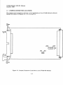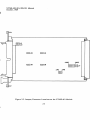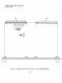
1
 XVME-400 / XVME-401 / XVME-490 / XVME-491
4-Channel Serial I/O Modules
USER’S MANUAL
ACROMAG INCORPORATED
30765 South Wixom Road
P.O. BOX 437
Wixom, MI 48393-7037 U.S.A.
Tel: (248) 295-0885
Fax: (248) 624-9234
Email: [email protected]
Copyright 2012, Acromag, Inc., Printed in the USA.
Data and specifications are subject to change without notice.
8500-970C XVME-400/40l/490/491 Manual
October, 1989
Chapter 1
INTRODUCTION
1.1 OVERVIEW
The XVME-400, XVME-401, XVME-490, and XVME-491 are Quad Serial I/O VMEbuscompatible modules which provide a VME system with four serial communications
channels. The XVME-400 and XVME-401 are single-high, while the XVME-490 and
XVME-491 are double-high. The XVME-400 and XVME-401 access the I/O through the
JKl and JK2 connectors on the module front panel, whereas the XVME-490 and
XVME-491 route their I/O to the VMEbus P2 connector.
The XVME-400 and XVME-490 each provide four RS-232C serial ports, while the
XVME-401 and XVME-491 each provide four RS-485/422A
serial ports. (Differences
among these modules are further detailed in Chapter 2, notably in Tables 2-1 and 2-2.)
Each module contains two 8530 Serial Communication Controller (SCC) chips, designated
SCC #l and SCC #2. The two SCC serial chips provide a variety of communication modes,
including asynchronous, byte-synchronous, and bit-oriented protocols. Each channel is
independently programmable and has its own baud rate generator.
The VMEbus interface directly maps the SCC chips into the short I/O address space,
starting on a jumper-selected 1 Kbyte boundary. The modules can also be jumpered to
generate an interrupt on any of the seven VMEbus interrupt levels. The two SCC chips
can generate a total of 16 different interrupt vectors.
Some features of the XVME-400/40l/490/491 modules include:
0
0
0
0
Four independent full-duplex serial I/O channels
RS-232C or RS485/422A operation
Serial channels
independently
configurable
for asynchronous,
monosynchronous, bisynchronous, or HDLC/SDLC message formats
Independent baud rate generators for each serial channel
Modem control
Receivers are quadruply buffered, transmitters double buffered
Complete VMEbus interrupter, jumper-selectable to any interrupt level
Programmable IACK vector, with vector alteration based on source of
interrupt
Line drivers for each channel are tri-stateable (controlled by software) to
allow multidrop operation (XVME-401 and XVME-491 only)
1-l
XVME-400/40l/490/491 Manual
October, 1989
1.2 MANUAL STRUCTURE
The chapters in this manual are structured as follows:
Chapter One -
A general description of the XVME-400/40 l/490/491 modules,
including complete functional and environmental specifications,
VMEbus compliance information, and block diagrams.
Chanter Two -
Module installation information, covering module-specific
system requirements, jumpers, and connector pinouts.
Chapter Three -
Details covering functional addressing, interrupt enabling, and
programming considerations and requirements.
Appendix A -
VMEbus connector and pin descriptions.
Appendix B -
Quick reference guide with jumper configurations.
Appendix C -
Block diagrams, assembly drawings, and schematics.
NOTE
This manual (XYCOM part # 74400-002) is part of a manual kit
(XYCOM part # 74400-001) that is being shipped with the
XVME-400/401/490/491 Modules. The kit also contains an 8530
Manual’ (referenced as XYCOM part # 74400-003).
This manual discusses module base addressing, register access
offsets, interrupt control, handshake control, and operational
mode/programming constraints. To better understand these topics,
is it recommended that you first read the 8530 Manual.
1 Z8030/Z8530 SCC Serial Communications Controller Technical Manual, Zilog, January, 1983.
l-2
XVME-400/401/490/491 Manual
October, 1989
1.4 MODULE SPECIFICATIONS
The following is a list of the operational and environmental specifications for the
XVME-400/40l/490/491 Modules.
Table l- 1. XVME-400/40l/490/491 Module Specifications
Characteristic
Specification
Number of Channels
4
Serial Device
Zilog 28530
Level
Compatibility:
XVME-400/490
XVME-401/491
RS-232C
RS-485/422A
Maximum Baud Rate:
Internal, async
Internal, sync
External, async
External, sync
57.6 Kbytes
500 Kbytes
57.6 Kbytes
500 Kbytes
Modem Control Signals Available
XVME-400/40 l/490
XVME-49 1
RTS, CTS, DCD, DTR
RTS, CTS, DCD
Power Requirements
XVME-400/490
+5V @ 1.1 A typ., 1.3 A max.
+12V @ 100 mA typ., 110 mA max.
+5V @ 1.4 A typ., 1.6 A max.
XVME-40 l/49 1
Temperature
Operating
Non-operating
0 to 65’C (32 to 149’F)
-40 to 85’C (-40 to 158’F)
Humidity
5 to 95% RH non-condensing
(Extremely low humidity may require
protection against static discharge.)
Altitude
Operating
Non-operating
Sea level to 10,000 ft. (3048 m)
Sea level to 50,000 ft. (15240 m)
1-5
XVME-400/40l/490/491 Manual
October, 1989
Table l- 1. XVME-400/40 l/490/49 1 Module Specifications (cont.)
Characteristic
Vibration
Operating
Non-operating
Shock
Operating
Non-operating
VMEbus Compliance
Specification
5 to 2000 Hz
0.0 15” peak-to-peak displacement
2.5 g peak acceleration
5 to 2000 Hz
0.030” peak-to-peak displacement
5.0 g peak acceleration
30
11
50
11
g peak acceleration,
msec duration
g peak acceleration,
msec duration
- Complies with VMEbus Specification, IEEE 1014
- A16:D8(0) DTB Slave
- Interrupt vector D08(0)DYN
- I(1) to I(7) interrupter (STAT), ROAK
- XVME-400/401: Single form factor
XVME-490/491: Double form factor
VMEbus Timing:
Typ(ns)
Max(ns)
DSO Asserted to DTACK Asserted (Read)
650 - 800
650 - 800
DSO Asserted to DTACK Asserted (Write)
IACKIN Asserted to DTACK Asserted (IACK) - 1100 1200
DSO Negated to DTACK Negated (All)
60
IACKIN Asserted to IACKOUT Asserted
300 - 400
1-6
100
XVME-400/40l/490/491 Manual
October, 1989
Chapter 2
INSTALLATION
2.1 INTRODUCTION
This chapter explains how to configure an XVME-400/401/490/491 Module prior to
installation in a VMEbus backplane. Included in this chapter is information on module
base address selection jumpers, module interrupt level selection jumpers, +5V, tri-state
jumpers, connector pinouts, and a brief outline of the physical installation procedure.
2.2 SYSTEM REQUIREMENTS
The XVME-400/40I Modules (single-high) or the XVME-490/491 Modules (double-high)
are VMEbus-compatible modules. To operate, each must be properly installed in a
VMEbus backplane.
The minimum system requirements for the operation of an XVME-400/401/490/491
Module are one of the following:
A)
A host processor properly installed on the same backplane.
A properly installed system controller module which provides the
following functions:
l
0
0
0
Data Transfer Bus Arbiter
System Clock Driver
System Reset Driver
Bus Timeout Module
OR
B)
A host processor which incorporates the system controller functions on-board.
An example of such a controller subsystem is the XYCOM XVME-010 System Resource
Module (SRM).
Prior to installing the XVME-400/401/490/491 Module, it will be necessary to configure
several jumper options. These options are:
1)
2)
3)
4)
Module base address within the short I/O address space
Address modifier codes to which the module will respond
Interrupt level
+5, tri-state jumpers (XVME-401 only)
2-1
XVME-400/401/490/491 Manual
October, 1989
2.4 XVME-400/401/490/491 MODULE JUMPER LIST
Table 2-1. XVME-400 and XVME-490 Jumper List
Use
Jumper
Jl
Determines whether the module will respond to supervisory or supervisory
and non-privileged short I/O VMEbus cycles (refer to Section 2.4.2 of this
manual).
JAl0-JAI5
Selects module base address on any one of the 64 1 Kbyte boundaries
within the short I/O address space (refer to Section 2.4.1 of this manual).
JAI-JA3
Selects the VMEbus interrupt level for the module (refer to Section 2.4.3
of this manual).
Table 2-2. XVME-401 and 491 Jumper List
Jumper
Use
Jl and J2
Brings the +5V supply to front-edge connectors JKl and JK2, respectively
(XVME-401 only; refer to Section 2.4.4).
J3-J6
Allows tri-stating of any of the channels (refer to Section 2.4.5).
J7
Determines whether the module will respond to supervisory or supervisory
and non-privileged short I/O VMEbus cycles (refer to Section 2.4.2).
JAl0-JAI5
Selects module base address on any one of the 64 1 Kbyte boundaries
within the short I/O address space (refer to Section 2.4.1).
JAI-JA3
Selects the VMEbus interrupt level for the module (refer to Section 2.4.3).
2.4.1 Base Address Jumpers (JA10-JA15)
The XVME-400/401/490/491 Module can be configured to be addressed at any one of the
64 1 Kbyte boundaries within the VME Short I/O address space by using jumpers JAl0
through 5 (see Figures 2-1, 2-2, 2-3, and 2-4 for the location of the jumpers on the
board) as shown above. Table 2-3 shows the Base Address Jumper Options.
2-6
XVME-400/40 I /490/49 1 Manual
October, 1989
2.4.2 Address Modifier Jumper (Jl or J7)
Each XVME-400/401/490/491 Module has one jumper that determines which address
modifier codes it will respond to. This jumper is Jl on the XVME-400/490 and J7 on the
XVME-401/491 (see Figures 2-1, 2-2, 2-3, and 2-4 for the jumper location). When this
jumper is in, the module will respond to supervisory short I/O bus cycles only. When this
jumper is out, the module will respond to both non-privileged and supervisory short I/O
bus cycles. Table 2-4 shows the relationship between this jumper and the address
modifiers.
Table 2-4. Addressing Options
1
Jumper
J1 (XVME-400/490), or
J7 (XVME-401/491)
Address Modifier to which the XVME-400/40l/490/491
Module will respond
In
(2DH) Supervisory only
Out
(2DH) Supervisory or (29H) Non-privileged
2.4.3 Interrupt Level Selection Jumpers (JAl-JA3)
The XVME-400/401/490/491 Module can either be configured to generate VMEbus
interrupts at levels 1-7 or the module interrupt capability can be completely disabled.
Table 2-5 shows how jumpers JAl-JA3 are used to determine the interrupt level status for
the XVME-400/40l/490/491 Module.
Table 2-5. Interrupt Level Jumper Positions
JA3
JA2
JA1
Interrupt Level Selected
In
In
In
In
out
out
out
out
In
In
out
out
In
In
out
out
In
out
In
out
In
out
In
out
None, VMEbus Interrupter disabled
Level 1
Level 2
Level 3
Level 4
Level 5
Level 6
Level 7
The module is shipped from the factory with jumpers JAl, JA2, and JA3 installed.
NOTE
If the module is never required to generate interrupts, JAI, JA2, and
JA3 should be installed to ensure that a programming bug will not
generate a VMEbus interrupt.
2-8
XVME-400/40 l/490/491 Manual
October, 1989
2.4.4 +5V Power Supply (Jl, J2; XVME-401 only)
On the XVME-401, jumpers Jl and J2 control whether the +5V supply is brought out to
front-edge connectors JKl and JK2. Table 2-6 indicates the functions of these jumpers.
Table 2-6. +5V Jumpers (XVME-401 only)
I
Jumper
Use
Jl
If Jl is installed, +5V will be connected to JKl (pin 47).
If Jl is removed, JKI-47 will float.
J2
If J2 is installed, +5V will be connected to JK2 (pin 47).
If J2 is removed, JK2-47 will float.
The +5V signals on the front-edge connector could be used to provide external line
termination by being used as a pull-up voltage, or for biasing.
2.4.5 Tri-stating the Serial Channels (J3-J6; XVMIE-401/491
only)
TO facilitate multidrop configurations, all drivers associated with a particular
communication channel may be tri-stated or enabled via SCC output pin RTS*. Each
channel has its own jumper to determine how the RTS* output affects line driver
enabling.
When a channel’s jumper is in the A position, the line drivers associated with that channel
for TT, RS, SD, and TR will be controlled by RTS*. When RTS* is negated (high voltage),
all line drivers associated with that channel will be tri-state. When RTS* is asserted, all
line drivers associated with that channel will be enabled. When a channel’s jumper is in
the B position, the line drivers associated with that channel will be enabled, regardless of
the state of the SCC output RTS*.
The jumper numbers related to the serial channel numbers are shown below and are all
shipped in the B position:
J3
J4
J5
J6
Channel
Channel
Channel
Channel
3
2
1
0
2.4.6 Daisy Chain Signals
Each slot in the VME backplane must propagate the Daisy Chain signals to the next
backplane slot. This occurs automatically if boards are installed in the slots. Where
boards are not installed, the appropriate backplane jumpers must be installed to continue
the signal path.
NOTE
Boards and jumpers should never both be installed in any one slot.
2-9
XVME-400/401/490/491 Manual
October, 1989
On the XVME-400/401, connector JKl carries the signals for Channels 0 and 2, while
connector JK2 carries the signals for Channels 1 and 3. On the XVME-490/491, the signals
for all four channels are carried on connector P2. All channels on all modules are
configured as DTE.
Sources of JKl /JK2. or P2 Connector Output Signals
(one set for each serial channel)
TXD/SD
SCC output pin TXD drives a line driver. Driver output is sent to this pin.
RTS/RS
SCC output pin RTS* drives a line driver. Driver output is sent to this pin.
TXC/TT SCC output pin TRXC drives a line driver. Driver output is sent to this pin.
DTR/TR SCC output pin DTR* drives a line driver. Driver output is sent to this pin.
NOTE
The RS232C signal names (XVME-400/490) are given to the left of
the slash, and the RS-485/422A
signal names to the right
(XVME-40l/491).
All line drivers invert the signal. For modem control lines, writing a 1 to the appropriate
SCC writer register bit will cause the output to be asserted. For TXD/SD and TXC/TT,
the polarity defined by RS-232C or RS-485 is provided.
Destinations of JKl /JK2. or P2 Connector Input Signals (one set for each serial channel)
RXD/RD This input pin is buffered by a line receiver and is driven to the SCC input pin
RXD.
CTS/CS
This input pin is buffered by a line receiver and is driven to the SCC input pin
CTS*.
RXC/RT This input pin is buffered by a line receiver and is driven to the SCC input pin
RTXC.
DCD/RR This input pin is buffered by a line receiver and is driven to the SCC input pin
DCD*.
All line receivers invert the signal. For modem control lines, a 1 will be read from the
appropriate SCC read control register bit when the input is asserted. For RXD/RD and
RXC/RT, the polarity defined by RS-232C or RS-485 is provided.
2-11
XVME-400/40l/490/491 Manual
October, 1989
2.5.1.1
JKl and JK2 Connector Pinouts on the XVME-400 (RS-232C)
Table 2-8 shows the XVME-400 pinout connectors JKl and JK2. These signals meet the
RS-232C specifications.
Table 2-8. XVME-400 Front Edge Connector Pin Definitions
Pin
Number
JKl
Signal
JK2
Signal
Signal
Direction
3
5
7
8
9
13
14
15
22
TXDO
RXDO
RTSO
RXCO Ch. 0
CTSO
GND
DRTO
DCDO
TXCO
TXDl
RXDl
RTSl
RXCl Ch. 1
CTSl
GND
DTRl
DCDl
TXCI
Transmit Data
Receive Data
Request To Send
Receiving Clock
Clear To Send
Ground
Data Terminal Ready
Data Carrier Detected
Transmitting Clock
OUT
IN
28
30
32
33
34
38
39
40
47
TXD2
RXD2
RTS2
RXC2 Ch. 2
CTS2
GND
DTR2
DCD2
TXC2
TXD3
RXD3
RTS3
RXC3 Ch. 3
Transmit Data
Receive Data
Request To Send
Receiving Clock
Clear To Send
Ground
Data Terminal Ready
Data Carrier Detected
Transmitting Clock
CTS3
GND
DTR3
DCD3
TXC3
OUT
IN
IN
OUT
IN
OUT
OUT
IN
OUT
IN
IN
OUT
IN
OUT
NOTE
All XVME-400 signal names are in the form XXXN where "N" is the
serial channel number and ‘(XXX” is the name of the signal.
All JKl and JK2 pin numbers not referenced are not connected.
The pinouts of JKl and JK2 allow a 50-conductor flat cable to be connected, split into
two 25-conductor sections, and have 25-pin D-type connectors installed on the two
25-conductor sections. The position of the signals relevant to the 25-pin D-type connectors
will be in accordance with the RS-232C definition (no line transitions are required):
TXD
RXD
RTS
CTS
GND
Pi n 2
Pi n 3
Pi n 4
Pi n 5
Pin 7
DCD Pin 8
RX C Pi n 1 7
DT R Pi n 20
TXC Pi n 24
2-12
XVME-400/40l/490/491 Manual
October, 1989
2.5.1.2
JKl and JK2 Connector Pinouts on the XVME-401 (RS-485/422A)
Table 2-9 shows the XVME-401 pinouts for connectors JKl and JK2. These signals meet
the RS-485/422A specifications.
Table 2-9. XVME-401 Front Edge Connector Pin Definitions
Pin
JKl
Number Signal
JK2
Signal
SDlB
SDlA
RDlB
RDIA
RSlB
RSlA
RTlB
Signal
1
2
5
6
7
8
9
10
11
12
16
17
18
19
20
21
24
25
SDOB
SDOA
RDOB
RDOA
RSOB
RSOA
RTOB
RTOA Ch. 0
CSOB
CSOA
TROB
TROA
RROB
RROA
TTOB
TTOA
SC0
SGO
26
27
30
31
32
33
34
35
36
37
41
42
43
44
45
46
47 (2)
49
50
SD2B
SD3B
SD2A
SD3A
RD2B
RD3B
RD2A
RD3A
RS2B
’ RS3B
RS2A
RS3A
RT2B
RT3B
RT2A
RT3A
CS2B Ch. 2
CS3B Ch. 3
CS2A
CS3A
TR2B
TR3B
TR2A
TR3A
RR2B
RR3B
RR2A
RR3A
TT2B
TT3B
TT2A
TT3A
+5v
+5v
SC2
SC3
SG2
SG3
RTlA
Ch. 1
CSlB
CSlA
TRIB
TRlA
RRlB
RRlA
TTlB
TTlA
SC1
SGl >
Transmit Data
Transmit Data
Receive Data
Receive Data
Request To Send
Request To Send
Receive Clock
Receive Clock
Clear To Send
Clear To Send
Data Terminal Ready
Data Terminal Ready
Data Carrier Detect
Data Carrier Detect
Transmit Clock
Transmit Clock
Logic Ground
Logic Ground
OUT
OUT
IN
IN
OUT
OUT
IN
IN
IN
IN
OUT
OUT
IN
IN
OUT
OUT
GND
GND
Transmit Data
Transmit Data
Receive Data
Receive Data
Request To Send
Request To Send
Receive Clock
Receive Clock
Clear To Send
Clear To Send
Data Terminal Ready
Data Terminal Ready
Data Carrier Detect
Data Carrier Detect
Transmit Clock
Transmit Clock
OUT
OUT
IN
IN
OUT
OUT
IN
IN
IN
IN
OUT
OUT
IN
IN
OUT
OUT
OUT
GND
GND
Logic Ground
Logic Ground s
2-13
Direction
XVME 400/401/490/491 Manual
October, 1989
NOTE
All XVME-401 signal names are in the form “XXNZ”, where “N” is
the channel number, “Z” is A or B based on the polarity of the
differential signal (as defined by RS-485), and “XX” is the name of
the signal. Also see Section 2.4.4.
All JKl and JK2 pin numbers not referenced are not connected.
2.5.2 Pl and P2 Connectors
The Pl and P2 connectors are the same physical type and have the same number of pins.
Both are 96-pin connectors consisting of three rows of 32 pins each. Like Pl, P2 is
mounted at the rear edge of the module. The pins for Pl contain the standard address,
data, and control signals necessary for the operation of VMEbus-defined NEXP modules.
(The signal definitions and pin-outs for connector Pl are found in Appendix A of this
manual.) The PI connector is designed to mechanically interface with a VMEbus defined
P 1 backplane.
The P2 connector (XVME-490/491 only) is a standard VMEbus P2 backplane connector.
It is designed to interface with a VMEbus defined P2 backplane.
2.5.2.1
P2 Connector Pinouts on the XVME-490 (RS-232C)
Table 2-10 shows the XVME-490 pinouts for connector P2. These signals meet the RS-232C
and VMEbus specifications.
Table 2-10. XVME-490 Rear Edge P2 Connector Pin Definitions
Pin #
9
10
11
12
13
14
15
16
Row A Signal
Row B Signal
Row C Signal
TXDO
RXDO
RTSO
RXCO Ch. 0
CTSO
DTRO
DCDO
TXCO
vcc
GND
NC
NC
NC
NC
NC
NC
GND
GND
GND
GND
GND
GND
GND
GND
TXDl
RXDl
RTSl
R X C I Ch.1
CTSl
DTRI
DCDl
TXCI
NC
NC
NC
GND
vcc
NC
NC
NC
GND
GND
GND
GND
GND
GND
GND
GND
2-I
,
XVME-400/40l/490/491 Manual
October, 1989
Table 2-10. XVME-490 Rear Edge P2 Connector Pin Definitions (Cont’d)
Pin #
Row A Signal
Row B Signal
Row C Signal
17
18
19
20
21
22
23
24
TXD2
RXD2
RTS2
RXC2 Ch. 2
CTS2
DTR2
DCD2
TXC2
NC
NC
NC
NC
NC
GND
NC
NC
GND
GND
GND
GND
GND
GND
GND
GND
25
26
27
28
29
30
31
32
TXD3
RXD3
RTS3
RXC3 Ch. 3
CTS3
DTR3
DCD3
TXC3
NC
NC
NC
NC
NC
NC
GND
vcc
GND
GND
GND
GND
GND
GND
GND
GND
NOTE
All P2 signal names are of the form “XXXN” where “N” is the serial
channel number and “XXX’ is the name of the signal. Signals with
the same “XXX” function identically with respect to the particular
channel.
2-15
XVME-400/40l/490/491 Manual
October, 1989
2.5.2.2
P2 Connector Pinouts on the XVME-491 (RS-485/422A)
Table 2-11 shows the XVME-491 pinouts for connector P2. These signals meet the
RS-485/422A
and VMEbus specifications.
T-able 2-11. XVME-491 Rear Edge P2 Connector Pin Definitions
Pin #
Row A Signal
Row B Signal
Row C Signal
1
2
3
4
5
6
8
TXDO+
TXCO+
RTSO+
RXDO+ Ch. 0
RXCO+
CTSO+
DCDO+
GND
vcc
GND
NC
NC
NC
NC
NC
NC
TXDOTXCORTSORXDORXCOCTSODCDOGND
9
10
11
12
13
14
15
16
TXDl+
TXCl+
RTSl+
RXDl+ Ch. 1
RXCl+
CTSl+
DCDl+
GND
NC
NC
NC
GND
vcc
NC
NC
NC
TXDITXClRTSlRXDlRXClCTSlDCDIGND
17
18
19 .
20
21 .
22
23
24
TXD2+
TXC2+
RTS2+
RXD2+ Ch. 2
RXC2+
CTS2+
DCD2+
GND
NC
NC
NC
NC
NC
GND
NC
NC
TXD2TXC2RTS2RXD2RXC2CTS2DCD2GND
25
26
27
28
29
30
31
32
TXD3+
TXC3+
RTS3+
RXD3+
RXC3+
CTS3+
DCD3+
GND
NC
NC
NC
NC
NC
NC
GND
vcc
TXD3TXC3RTS3RXD3RXC3CTS3DCD3GND
.
7
Ch. 3
I
NOTE
All XVME-401 signal names are in the form “XXNZ”, where “N” is
the channel number, “Z” is + or - based on which half of the signal
it is, and “XX” is the name of the signal.
2-16
XVME-400/401/490/491
October, 1989
2.6
MODULE
Manual
INSTALLATION
XYCOM XVME modules are designed to comply with all physical and electrical VMEbus
backplane
specifications. The XVME-400/401 Modules are single-high and single-wide
and, as such, only require the Pl backplane. The XVME-490/491 Modules are doublehigh and single-wide, and use the PI and P2 backplane.
CAUTION
Never attempt to install or remove any boards before turning off
the power to the bus, and all related external power supplies.
Prior to installing a module, determine and verify all relevant
jumper configurations, and all connections to external devices or
power supplies. (Check the jumper configuration against the
diagrams and lists in this manual.)
To install a board in the cardcage, perform the following steps:
1)
Make certain that the particular cardcage slot which you are going to use is
clear and accessible.
2)
Center the board on the plastic guides in the slot so that the handle on the
front panel is towards the bottom of the cardcage (XVME-400/401 only).
3)
Push the card slowly toward the rear of the chassis until the connectors engage
(the card should slide freely in the plastic guides).
4)
Apply straight-forward pressure to the handle located on the front panel of the
module until the connector is fully engaged and properly seated.
NOTE
Do not use excessive pressure or force to engage the
connectors. If the board does not properly connect with
the backplane, remove the module and inspect all
connectors and guide slots for possible damage or
obstructions.
5)
Once the board is properly seated, secure it to the chassis by tightening the two
machine screws at the top and bottom of the board.
2-17
XVME-400/40l/490/491 Manual
October, 1989
Chapter 3
MODULE PROGRAMMING
3.1
INTRODUCTION
This chapter will discuss the addressing and initialization procedures for programming
the XVME-400/40l/490/491 Modules. In order to demonstrate the correct sequence of
initialization for the serial channels contained in the SCC chips, two programming
examples (with comments) have been incorporated in this chapter. For a complete
explanation of how to program and maximize the functionality
of the SCC chip, refer to
.
the accompanying SCC Manual.
Each module contains four serial communication channels, designated as channels 0, 1,2,
and 3. Each SCC has two serial channels designated by Zilog as channels A and B. The
SCC channels map into the module channels as follows:
Module Channel Number
0
1
2
3
SCC Channel
Priority
SCC #1, Channel A
SCC #1, Channel B
SCC #2, Channel A
SCC #2, Channel B
Highest
Lowest
Throughout this document, the module channel number (0, 1, 2, 3) will be referenced.
For interrupt operation, the serial channels are prioritized, with channel 0 having the
highest priority and channel 3 having the lowest priority. Therefore, for a given
application, the serial links running at higher data rates should be assigned to module
channels with higher interrupt priority.
3.2
MODULE
ADDRESSING
The XVME-400/401/490/491 Modules are designed to be addressed within the VMEbusdefined 64 Kbyte short I/O address space. When the XVME-400/401/490/491 Module is
installed in the system it will occupy a 1 Kbyte block of the short I/O address space. The
base address decoding scheme for the XVME I/O modules is such that the starting address
for each board resides on a 1 Kbyte boundary. Thus, there are 64 possible locations (1
Kbyte boundaries) in the short I/O address space which could be used as the base address
for the XVME-400/401/490/491 Module. (Refer to Section 2.4.1 for the list of base
addresses and their corresponding jumper configurations).
All register locations within the SCC devices are given specific addresses which are offset
from the module base address. Thus, a specific register address in one of the SCC chips
can be accessed by adding the specific register offset to the module base address. For
example, the offset specified for the Serial Channel 2 Data Register is 07H, and if the
module base address is jumpered to 1OOOH, the register can be accessed at 1007H.
3-1
XVME-400/40l/490/491 Manual
October, 1989
Module Base Address
Register
Register Offset
1OOOH
=
07H
+
I
Serial Channel 2 Data
1007H
NOTE
The XVME-400/401/490/491 is an odd byte only slave,
and as such, the module will not respond to even address,
single-byte accesses. However, word accesses may be
used, with the understanding that only the odd byte of
the word is used to exchange data. If word accesses are
used, the register offsets listed in Table 3-1 would all be
decremented by 1.
Table 3-1 lists the offsets for the internal registers of all four serial channels on the
XVME-400 (two channels per SCC serial chip).
.
Table 3-1. Register Offsets
Off set Address
Hex
Decimal
1
3
5
7
9
B
D
F
1
3
5
7
9
11
13
15
Module Register
Serial
Serial
Serial
Serial
Serial
Serial
Serial
Serial
Channel
Channel
Channel
Channel
Channel
Channel
Channel
Channel
3
3
2
2
1
1
0
0
Control Register
Data Register
Control Register
Data Register
Control Register
Data Register
Control Register
Data Register
(SCC #2 Channel B)
(SCC #2 Channel B)
(SCC #2 Channel A)
(SCC #2 Channel A)
(SCC #l Channel B)
(SCC #l Channel B)
(SCC #l Channel A)
(SCC #l Channel A)
The registers in the 8530 are accessed in a two-step process. The first step is to write a
pointer to one of the four control registers listed in Table 3-l. After the pointer is written
to a control register, the next read or write to the same control register will access the
desired 8530 register. Refer to the 8530 Manual for a description of the 8530 registers
and their pointers.
Single-step access of a data register is performed by reading or writing to any of the four
data registers. The XVME-400/401/490/491 will automatically set D/C high and will
access the 8530 registers RRS or WRS directly, independent of the state of the pointer bits.
3-2
XVME-400/40l/490/491 Manual
October, 1989
3.3 MODULE INTERRUPT SOURCES
There are twelve sources of interrupts on the XVME-400/401/490/491 (three sources from
each serial channel). When enabled, each of these sources can generate VMEbus interrupts
on the level specified by jumpers JAI-JA3. The interrupt sources are prioritized during
the VMEbus IACK cycle, as shown in Table 3-2.
Table 3-2. Priority of Local Interrupt Sources
Channel
Interrupt Source
Priority
0
0
0
1
1
1
2
2
2
3
3
3
Receive Character Available
Transmit Buffer Empty
External/Status
Change
Receive Character Available
Transmit Buffer Empty
External/Status
Change
Receive Character Available
Transmit Buffer Empty
External/Status
Change
Receive Character Available
Transmit Buffer Empty
External/Status
Change
Highest
Lowest
When the module responds to a VMEbus IACK cycle, the IACK vector is acquired from
the appropriate SCC chip and driven onto the VMEbus. Since each SCC can produce 8
vectors, SCC IACK vector register (WR2) must be initialized before interrupts are enabled.
When programmed to include status in the IACK vector (WR9:DO=l), the status high/low
bit (WR9:D4) determines whether IACK vector bits 3,2,1 or bits 4,5,6 will contain status
information. The status information returned in IACK vector is shown in Table 3-3 on
the following page:
3-3
XVME-400/40l/490/491 Manual
October, 1989
FIFO, the Receive Character Available IACK vector will be acquired. If there is a special
receive condition associated with the character on top of the FIFO, the Special Receive
Condition IACK vector will be acquired.
There are four special receive conditions:
1)
2)
3)
4)
Receive overrun
Framing error (ASYNC only)
End of frame (SLDLC only)
Parity error (if WRl:D2=1)
For interrupt driven operation, it is suggested that an interrupt on all receive characters
or special conditions be programmed along with programming parity errors as a special
condition. When programmed in this mode, and the receive character available IACK
vector is acquired, it is guaranteed that no special conditions exist for the received byte
on top of the FIFO. Therefore, RR1 does not have to be checked after every receive byte.
This eliminates two VMEbus cycles from the receive character interrupt service routine.
When a special receive condition IACK vector is acquired, the following sequence should
be executed in the specified order: i
1)
2)
3)
3.3.2
Read RR1 to determine the source of special condition.
Issue reset error command in WRO to clear errors.
Read the data register.
Transmit Buffer Empty Interrupts
Each of the four channels has its own Transmit Character available: IE, IP, and IUS
internal bits. The IE bit is set (i.e., transmit buffer interrupts are enabled) by setting
WRl:Dl. If these interrupts are enabled, two events can cause this IP to become set: when
the transmit buffer is ready to receive a byte (RRO:D2=1),
and after the CRC is sent in
synchronous modes (RRO:D2=0).
The IP is reset by writing to the data register or by
issuing the Reset TxINT Pending command WRO.
3.3.3
External/Status
Interrupts
There are six sources of interrupts that share this IP:
1)
2)
3)
4)
5)
6)
Break/Abort
Underrun/EOM
CTS
DCD
Sync/Hunt
Zero Count
Each of these sources has a separate enable bit in WR15 and has a separate status bit in
RRO. The master external/status interrupt enable bit is WRl:DO. In general, when a status
bit changes state and is enabled, the external/status IP will be set and cause an interrupt.
The IP is reset by issuing the Reset External/Status Interrupt command in WRO.
3-5
XVME-400/40l/490/491 Manual
October, 1989
3.4 CLOCKING OPTIONS
This section describes the transmit and receive clocking options for the serial channels.
It applies to all four independently configurable serial channels.
3.4.1
Hardware Configurations
The SCC receive clock input pin, RTXC, is driven from line receivers which are connected
to the JK RT input (see Section 2.5). Therefore, the frequency of SCC pin RTXC is
determined by the external clock connected to the RXC/RT input pin. This clock input
signal will be referred to as RXC/RT in this section. The crystal oscillator feature of the
SCC is not used.
The SCC transmit clock pin, TRXC, is used as an output. It is buffered by line drivers
and driven to a TXC/TT output on a front edge connector. The SCC pin TRXC must be
programmed as an output (WRl 1) and must not be selected as an internal SCC clock source.
This clock output signal is referred to as TXC/TT in this section.
In all possible clocking combinations, the polarities of the clock signals TXC/TT and
RXC/RT are in accordance with the RS-232C or RS-485 standards.
The SCC’s clock pin PCLK is connected to a 3.6864 MHz clock. This frequency allows the
baud rate generator to produce most of the popular baud rates used for serial
communications.
3-6
XVME-400/40l/490/491 Manual
October, 1989
3.4.2
Baud Rate Generator
The SCC contains a programmable baud rate generator whose output can be used as
internal timing sources. The baud rate generator’s clock input may be programmed to
connect to either the RXC/RT signal or PCLK (WR14). A 16-bit time constant can be
programmed into WR13 (most significant byte) and WR12 (least significant byte) to select
the baud rate generator’s output frequency. The following equations show the baud rate
generator’s output frequency as a function of the time constant, and vice versa:
If baud rate generator input is RXC or RT (WR14:Dl=O):
Time Constant = (Frequency of RXC/(2 * CM * Baud Rate)) -2
Baud Rate = Frequency of RXC/(2 * CM * (Time Constant + 2))
If baud rate generator input is PCLK (WR14:Dl=l):
(PCLK = 3.6864 MHz)
Time Constant = (1.8432 MHz/(CM * Baud Rate)) -2
Baud Rate = 1.8432 MHz/(CM * (Time Constant + 2))
In the above equations, CM is the clock multiplier used by the transmitter and receiver
(i.e., CM=1 6 for X 16 clock multiplier).
The output of the baud rate generator can be used as the transmitter clock source and/or
the receiver clock source, and it may also be sent to the TXC/TT output. Any
combination of these three may be used.
3.4.2.1
Programming the Baud Rate Generator
The following steps should be followed in the specified order to program the baud rate
generator:
1)
2)
3)
4)
3.4.2.2
Disable the baud rate generator (WR14:D0-0).
Load WR12 and WR13 with the desired time constant.
Select baud rate generator clock source:
WR14:Dl = 0 for RXC/RT
WR14:Dl = 1 for PCLK
Enable the baud rate generator, WR14:D0=l.
Time Constant Examples
The following tables show the time constants required for popular baud rates when PLCK
is used as the baud rate generator input. Two tables are shown, one for synchronous (1X
clock) and one for asynchronous (16X clock). These particular constants are shown for
illustration only. Any time constant may be used.
3-7
XVME-400/40l/490/491 Manual
October, 1989
Table 3-4. Typical Time Constraints for Synchronous (xl) Clock
Baud Rate
76.8 K
38.4 K
19.2 K
9600
7200
4800
3600
2400
1800
1200
600
300
Time Constant
(Base 10)
I
22
46
94
190
254
382
510
766
1022
1534
3070
6142
WR13 Value
(Hex)
00
00
00
00
00
01
01
02
03
05
OB
17
WR12 Value
(Hex)
16
2E
5E
BE
FE
7E
FE
FE
FE
FE
FE
FE
Table 3-5. Typical Time Constraints for Asynchronous (x16) Clock
Baud Rate
19200
9600
7200
4800
3600
2400
1800
1200
600
300
150
75
50
Time Constant
(Base 10)
WR13 Value
(Hex)
4
IO
14
22
30
46
62
94
190
382
766
1534
2302
00
00
00
00
00
00
00
00
00
01
02
05
08
3-8
04
OA
OE
16
1E
2E
3E
5E
BE
7E
FE
FE
FE
XVME-400/401/490/491 Manual
October, 1989
3.5
SERIAL CHANNEL CLOCK CONFIGURATIONS
The receiver and/or transmitter can be independently programmed to accept their clock
source from any of the following: the RXC/RT signal, the baud rate generator, or the
digital phase locked loop (see the SCC manual). (TXC/TT may not be programmed as a
clock source.) The receiver option is specified in WRl l:D6,D5, the transmitter in
WRl l:D4, D3.
The TXC/TT output signal may be programmed to output any of the following: the baud
rate generator, the digital phase lock loop, or the transmitter’s clock. This is selected via
WRl l:Dl,DO.
Any combination of clock rate and baud rate options may be used in synchronous or
asynchronous modes. Four typical examples are given below:
1)
Asvnchronous Operation
The baud rate generator is used as the transmitter and receiver clocks. The master
clock signal received on the pin PCLK is used for the generator’s input. The external
clock’s RXC/RT and TXC/TT are not used.
2)
Svnchronous Operation. External Transmitter and Receiver Timing Definition
The RXC/RT clock input is used for the transmitter and receiver clocks. TXC/SD
output will be synchronized to the clock input on RXC/RT. RXD/RT input will be
sampled by clock input RXC/RT. The baud rate generator is not used.
3)
Svnchronous Operation. Internal Transmitter and Receiver Timing Definition
The baud rate generator is used for the transmitter and receiver clocks. TXC/TT
output signal is programmed to output the baud rate generator. TXC/SD output will
be synchronized to the clock output TXC/TT. RXD/RD input will be sampled by
clock output TXC/TT.
4)
Svnchronous Operation. External Receiver Timing Definition and Internal
Transmitter Timing Definition
The baud rate generator is used for the transmitter clock and is sent out on the
TXC/TT line. The RXC/RT signal is used for the receiver clock. TXD/SD output
will be synchronized to the clock output TXC/TT. RXD/RD input will be sampled
by clock input RXC/RT.
36
.
MODULE RESET OPERATION
The module is reset by the assertion of VMEbus signal SYSRESET*. In response, the
module will reset its VMEbus interface and the SCCs. Refer to the SCC technical manual
for SCC reset operation.
3-9
XVME-400/40l/490/491 Manual
October, 1989
3.7
GENERAL
PROGRAMMING
CONSIDERATIONS
This section outlines programming rules which apply to all modes of operation. These
constraints are dictated by hardware configurations.
WRl -
Set D7, D6, D5 to 0, 1, 0. This will disable the DMA and WAIT features of the
SCCs. Polled or interrupt operation must be used.
WR4-
D5, D4 must not be programmed for external sync modes of operation.
WR9-
Set Dl to 0. This will enable the interrupt vector feature of the SCC. There
are no other sources of IACK vectors on the module.
WRll-
Set D7 to 0. This will disable the external crystal oscillator feature of the SCC.
The SCC pin /TRXC must not be programmed as a clock source for the receiver
(D6,D5) or the transmitter (D4,D3). Set D2 to 1 to select the /TRXC pin as an
output.
WR14 -
Set D2 to 0 to program the DTR/REQ pin to the DTR function.
Asynchronous
3.7.1
Operation
Initialization
This section describes the steps required to set up the SCCs for asynchronous operation.
These steps apply to any channel and should be followed in the specified order.
1)
Issue the Channel Reset command (WR9:D7,6).
2)
Set WR4 as follows clock mode in D7,D6 (16X is suggested); number of stop bits
in D3,D2; and parity odd/even/enable in Dl, DO.
3)
Set WR3 as follows: number of receive bits/character in D7,D6;
as required in D5; receiver disable DO=O.
4)
Set WR5 as follows: state of DTR and CTS in D7, Dl; number of transmit
bits/character in D6,D5; transmitter disable D3=0.
5)
Set WRl0 for NRZ D6,D5=0,0.
6)
Set interrupt or polled operation (refer to Section 3.3).
7)
Set clocking options (refer to Section 3.4).
8)
Enable receiver (WR:DO) and transmitter (WR5:D3)
3-10
as required.
auto enables
XVME-400/40l/490/491 Manual
October, 1989
Synchronous
3.7.2
Operation
Initialization
This section describes the steps required to set up the SCCs for synchronous operation.
These steps apply to any channel and should be followed in the specified order.
1)
Issue the Channel Reset command (WR9:D7,6).
2)
Set WR4 as follows: X.1 clock mode D7,D6=0,0; type of sync D5,D4; sync mode
enabled D3,D2=0,0; parity odd/even/enable in D1,DO.
3)
Set WRI0 as required.
4)
Set WR6 and WR7 to the sync character or SDLC address as required.
5)
Set WR3 as follows:
number of receive bits/character in D7,D6;
D5,D4,D3,D2,D 1 as required; receiver disabled DO=O.
6)
Set WR5 as follows: state of DTR and CTS in D7,Dl; number of transmit
bits/character in D6,D5; D4,D2,D0 as required; and transmitter disabled D3=0.
7)
Set WR14 as required.
8)
Set interrupt or polled operation (refer to Section 3.3).
9)
Set clocking options (refer to Section 3.4).
10)
Enable receiver (WR3:DO)
and transmitter (WR5:D3)
3-11
as required.
-
XVME-400/40l/490/491 Manual
October, 1989
3.8 PROGRAMMING EXAMPLE
********************************************************************************
*
*
XVME-400/40 l/490/49 1 Sample Program
*
*
*
Polled mode - Asynchronous Operation
*********$**I*****$**********************~***************************************
*
*
EQUATES
*
*********************************************************************************
BASE
EQU
$OOFFOOOO
SCClAC
EQU
STACK
EQU
ORG
START
* Base address of module
* Start of stack
* SCC #l control register
$A00
BASE+13
$800000
M0VEA.L #STACK,A7
M0VE.W #$2000,SR
* Load stack pointer
* Load status register
* Configure cha nnel A of SCC #l
LEA.L
* Load address of module
* 9600 baud time constant
INIT * Initialize channel A
M0VE.W
SCClAC,AO
#$000A,D7
BSR.S
ASYNC
* Read a character from channel A of SCC #l
LOOP
LEA.L
BSR
SCClAC,A3
RPOLA
* Load address of SCC control reg.
* Get a character
* Write a charac ter to channel A of SCC #l
LEA.L
BSR
SCC 1 AC,A2
TPOLA
BSR.S
LOOP
* Load address of SCC control reg.
* Echo the character
3-12
XVME-400/40l/490/491 Manual
October, 1989
*********************************************************************************
*
*
*
*
This subroutine will initialize the specified SCC channel for asynchronous
operation.
On entry:
A0.L = SCC control register address
D7.W = [ WR13 ] WR12 ] baud rate time constant
*
On exit:
*
Transmitter and receiver enabled
*********************************************************************************
ASYNC
INIT:
M0VE.B #9,(A0)
M0VE.B #$8O,(AO)
M0VE.B #4,(A0)
M0VE.B #%01000101,(A0)
* Set WR9
* Reset channe 1 A, SCC #l
* Set WR4: X16 clock, 1 stop bit
* Odd parity enabled
M0VE.B
M0VE.B
#3,(A0)
#%11000000,(A0)
* Set WR3: 8 RX bits disabled
* No auto enable
M0VE.B
M0VE.B
#5,(A0)
* Set WR5: DTR and RTS asserted
* 8 TX bits, TX disabled
M0VE.B
M0VE.B
#l,(AO)
* Set WRl: DMA/WAIT pins
* Set RX,TX, ext. int. disabled
* Parity = special condition
M0VE.B
M0VE.B
#2,(A0)
* Set WR2
* IACK vector = $40
M0VE.B
M0VE.B
#9,(A0)
* Set WR9: status 1o w, MIE set
* DLC=O 9 IACK vector variable
M0VE.B
M0VE.B
#1O,(AO)
#0,(AO)
* Set WRl0 to NRZ
M0VE.B
M0VE.B
#1l,(AO)
#%0l0l0ll0,(A0)
* Set WRll: no XTAL
* RX TX clock=BRG
* TRXC=BRG
R0R.W
M0VE.B
M0VE.B
#8,D7
#13,(AO)
D7,(AO)
* Set WR13: High order
* Time constant
#%ll lOOOlO,(AO)
#%01000100,(A0)
#$4O,(AO)
#%00001001,(A0)
3-13
XVME-400/40l/490/49I Manual
October, 1989
R0L.W
M0VE.B
M0VE.B
M0VE.B
M0VE.B
M0VE.B
M0VE.B
#8,D7
#12,(AO)
D7,(AO)
#14,(AO)
#2,(AO)
#14,(AO)
#3,(A0)
* Set WR12: Low order
* Time constant
M0VE.B
M0VE.B
#15,(AO)
#0,(A0)
* Set WR15: Disable all external
* interrupts
M0VE.B
M0VE.B
#3,(A0)
* Enable receiver
M0VE.B
M0VE.B
#5,(AO)
*
* Set WR14
* BRG source=PCLK
* Enable BRG
#%11000001,(A0)
#%l1101010,(A0)
Enable transmitter
RTS
********************************************************************************
*
I
This routine will transmit a byte in polled mode.
*
*
On entry:
*
A2 contains the address of the command
*
register of the SCC channel used for
*
transmitting.
*
*
D2.B contains the byte to be transmitted.
*
******************************************************************************
TPOLA
MOVEML DO/D 1 /A 1 ,-(SP)
TXPOLL M0VE.B (A2),DO
BTST
#2,DO
BEQ.S
TXPOLL
TXBFE
M0VE.B D3,2(A2)
*
*
*
*
*
*
TXIT
* Restore registers
MOVEML (SP)+,DO/Dl / A 1
RTS
3-14
Save registers
Read the contents of RR0
Is TX buffer empty?
No, then poll again
Yes, move character to transmit
data register
XVME-400/40I /490/491 Manual
October, 1989
********************************************************************************
*
*
This routine will receive a byte of data in polled mode.
*
*
*
On entry:
A3 contains the address of the command
register of the SCC channel used for
receiving.
On exit:
D3.B contains the byte which was received.
*********************************************************************************
RPOLA
M0VE M.L DO/D 1 /A 1 ,-(SP)
RXPOLL M0VE.B (A3),DO
BTST
#O,DO
RXPOLL
BEQ.S
RXCHA M0VE.B 2(A3),D3
*
*
*
*
*
RXIT
* Restore registers
MOVEM.L (SP)+,D0/D 1 /A 1
RTS
END
3-15
Save registers
Read the contents of RR0
Is a character available?
No, then try again
Get the character
XVME-400/40l/490/491 Manual
October, 1989
*
*
*
*
*
*
This routine will initialize the specified SCC channel to asynchronous
operation. A hardware reset is assumed before code is executed.
IN: A0.1 = SCC Control Register Address
D7.W = [ WR13 I WR12 ] Baud Rate Time Constant
*
OUT:
Transmitter and receiver enabled.
*
All channel interrupts disabled.
*
IACK Vector Register set to $40, MIE bit set, DLC bit reset.
*
Variable IACK Vector enabled, low status
*
Xl6 Clock mode, 1 stop bit, odd parity enabled
*
Transmitter and receiver set to 8 bits/character
*
No auto enables
*
DTR/TR and RTS/RS asserted
*
Receive clock, transmit clock, and TXC/TT programed for
*
BRG Output
*
BRG clock = PCLK
*
*********************************************************************************
ASYNC-INIT:
M0VE.B
M0VE.B
#4,(A0)
#%01000101,(A0)
*
M0VE.B
M0VE.B
#3,(A0)
#$l 1 OOOOOO,(AO)
*
M0VE.B
M0VE.B
#5,(A0)
#%11l000l0,(A0)
*
M0VE.B
M0VE.B
#1,(A0)
#%01000100,(A0)
*
*
*
*
*
*
M0VE.B
M0VE.B
*
*
Set WR4: Xl6 clock, 1 stop bit
Odd parity enabled
Set WR3: 8 RX bits
No auto enable, RX disabled
Set WR5: DTR & RTS asserted,
8 TX bits, TX disabled
Set WRI: DMA/WAIT pins,
RX, TX, EXT INT disabled,
Parity = Special condition
WR2
IACK Vector = $40
M0VE.B
M0VE.B
#9,(A0)
#%00001001,(A0)
*
*
Set WR9: Status Low, MIE set,
DLC=O, IACK Vector variable
M0VE.B
M0VE.B
#l0,(A0)
#l0,(A0)
*
Set WRl0 to NRZ
M0VE.B
M0VE.B
#l l,(A0)
#%0l0l0l
lit
Set WRll: No XTAL,
RX, TX Clock = BRG,
TRXC = BRG
l0,(A0)
*
*
3-16
XVME-400/40l/490/491 Manual
October, 1989
R0R.W
M0VE.B
M0VE.B
#8,D7
#13,
D7,(AO)
* Set WR13 = High order
* Time constant
R0L.W
M0VE.B
M0VE.B
#8,D7
#12,(AO)
D7,(AO)
* Set WR12 = Low Order
* Time constant
M0VE.B
M0VE.B
M0VE.B
M0VE.B
#14,(A0)
#2,(A0)
#14,(A0)
#3,(A0)
* Set WR14:
* BRG source = PCLK
M0VE.B
M0VE.B
#15,(A0)
#0,(A0)
* Set WR15: Disable all external
* Interrupts
M0VE.B
M0VE.B
#3,(A0)
#%11000001,(A0)
* Enable receiver
M0VE.B
M0VE.B
#5,(A0)
#%11 l0l0l0,(A0)
* Enable transmitter
* Enable BRG
RTS
3-17
XVME-400/40l/490/491 Manual
October, 1989
Appendix A
VMEbus CONNECTOR/PIN DESCRIPTIONS
Pl BACKPLANE CONNECTOR
All the modules have the rear-edge connector PI, which is a 96-pin bus connector
consisting of three rows of 32 pins each. (Row A is physically closest to the board. See
Table A-2). The signals carried by connector Pl are the standard address, data, and
control signals required for a Pl backplane interface as defined by the VMEbus
Table A-l identifies and defines the signals carried by the Pl connector.
specification.
Table A-l. PI - VMEbus Signal Identification
Signal
Mnemonic
Connector
and
Pin Number
ACFAIL*
lB:3
AC FAILURE: Open-collector driven signal which
indicates that the AC input to the power supply is no
longer being provided, or that the required input voltage
levels are not being met.
IACKIN*
lA:21
INTERRUPT ACKNOWLEDGE IN: Totem-pole driven
signal. IACKIN* and IACKOUT* signals form a daisy-
Signal Name and Description
chained acknowledge. The IACKIN* signal indicates to
the VME board that an acknowledge cycle is in progress.
IACKOUT*
AM0-AM5
1 A:22
A:23
B:16,17,
8,19
INTERRUPT ACKNOWLEDGE OUT: Totem-pole driven
signal. IACKIN* and IACKOUT* signals form a daisychained acknowledge. The IACKOUT* signal indicates to
the next board that an acknowledge cycle is in progress.
ADDRESS MODIFIER (bits 0-5): Three-state driven lines
that provide additional information about the address bus,
such as: size, cycle type, and/or DTB master identification.
C:14
AS*
ADDRESS STROBE: Three-state driven signal that
indicates a valid address is on the address bus.
A-l
XVME-400/40l/490/491 Manual
October, 1989
Table A-l. VMEbus Signal Identification (cont’d)
Connector
and
Pin Number
Signal Name and Description
A0I-A23
1A:24-30
lC:15-30
ADDRESS BUS (bits l-23): Three-state driven address lines
that specify a memory address.
A24-A3 1
2B:4-11
ADDRESS BUS (bits 24-31): Three-state driven bus
expansion address lines.
BBSY*
1B:l
BUS BUSY: Open-collector driven signal generated by the
current DTB master to indicate that it is using the bus.
BCLR*
IB:2
BUS CLEAR: Totem-pole driven signal generated by the
bus arbitrator to request release by the DTB master if a
higher level is requesting the bus.
BERR*
1C:ll
BUS ERROR: Open-collector driven signal generated by a
slave. It indicates that an unrecoverable error has occurred
and the bus cycle must be aborted.
BG0IN*BG3IN*
1B:4,6,
8,l0
BUS GRANT (0-3) IN: Totem-pole driven signals generated
by the Arbiter or Requesters. Bus Grant In and Out signals
form a daisy-chained bus grant. The Bus Grant In signal
indicates to this board that it may become the next bus
master.
BG0OUT*BG3OUT*
lB:5,7,
9,ll
BUS GRANT (0-3) OUT: Totem-pole driven signals
generated by Requesters. These signals indicate that a
DTB master in the daisy-chain requires access to the bus.
Signal
Mnemonic
A-2
XVME-400/40l/490/491 Manual
October, 1989
Table A-1. VMEbus Signal Identification (cont’d)
Signal
Mnemonic
Connector
and
Pin Number
BR0*-BR3*
lB:12-15
BUS REQUEST (0-3): Open-collector driven signals
generated by Requesters. These signals indicate that a
DTB master in the daisy-chain requires access to the bus.
DS0*
IA:13
DATA STROBE 0: Three-state driven signal that indicates
during byte and word transfers that a data transfer will
occur on data buss lines (D00-D07).
DSl*
IA:12
DATA STROBE 1: Three-state driven signal that indicates
during byte and word transfers that a data transfer will
occur on data bus lines (D0-D15).
DTACK*
lA:16
DATA TRANSFER ACKNOWLEDGE: Open-collector
driven signal generated by a DTB slave. The falling edge
of this signal indicates that valid data is available on the
data bus during a read cycle, or that data has been
accepted from the data bus during a write cycle.
D00-D15
lA:l-8
lC:l-8
DATA BUS (bits 0-15): Three-state driven, bi-directional
data lines that provide a data path between the DTB
master and slave.
GND
lA:9,11,
15,17,19,
1B:20,23,
lC:9
2B:2,12,
22,3 1
GROUND
Signal Name and Description
A-3
XVME-400/40l/490/491 Manual
October, 1989
Table A-l. VMEbus Signal Identification (cont’d)
Signal
Mnemonic
Connector
and
Pin Number
IACK*
1A:20
INTERRUPT ACKNOWLEDGE: Open-collector or threestate driven signal from any master processing an interrupt
request. It is routed via the backplane to slot 1, where it
is looped-back to become slot 1 IACKIN* in order to start
the interrupt acknowledge daisy-chain.
IRQl*IRQ7*
1B:24-30
INTERRUPT REQUEST (1-7): Open-collector driven
signals, generated by an interrupter, which carry
prioritized interrupt requests. Level seven is the highest
priority.
LWORD*
lC:l3
LONGWORD: Three-state driven signal indicates that the
current transfer is a 32-bit transfer.
(RESERVED)
2B:3
RESERVED: Signal line reserved for future VMEbus
enhancements. This line must not be used.
SERCLK
lB:21
A reserved signal which will be used as the clock for a
Signal Name and Description
serial communication bus protocol which is still being
finalized,
SERDAT
1B:22
A reserved signal which will be used as the transmission
line for serial communication bus messages.
SYSCLK
1A:l0
SYSTEM CLOCK: A constant 16-MHz clock signal that is
independent of processor speed or timing. It is used for
general system timing use.
A-4
XVME-400/401/490/491 Manual
October, 1989
Table A-l. VMEbus Signal Identification (cont’d)
Signal
Mnemonic
Connector
and
Pin Number
SYSFAIL*
1C:l0
SYSTEM FAIL: Open-collector driven signal that indicates
that a failure has occurred in the system. It may be
generated by any module on the VMEbus.
SYSRESET*
lC:12
SYSTEM RESET: Open-collector driven signal which, when
low, will cause the system to be reset.
WRITE*
lA:14
WRITE: Three-state driven signal that specifies the data
transfer cycle in progress to be either read or write. A
high level indicates a read operation, a low level indicates
a write operation.
+5V STDBY
lB:31
+5 VDC STANDBY: This line supplies +5 VDC to devices
requiring battery backup.
+5v
1A:32
lB:32
1C:32
2B:l,l3,32
+5 VDC POWER: Used by system logic circuits.
+12v
lC:31
+12 VDC POWER: Used by system logic circuits.
-12v
lA:31
-12 VDC POWER: Used by system logic circuits.
Signal Name and Description
A-5
XVME-400/40 l/490/49 1 Manual
October, 1989
Table A-2. Pl Signal Identification
Pin
Row A
Signal
Mnemonic
Row B
Signal
Mnemonic
Signal
Mnemonic
1
2
3
4
5
6
7
8
9
10
11
12
13
14
15
16
17
I8
19
20
21
22
23
24
25
26
27
28
29
30
31
32
D00
DO1
DO2
DO3
DO4
DO5
DO6
DO7
GND
SYSCLK
GND
DSl*
DSO*
WRITE*
GND
DTACK*
GND
AS*
GND
IACK*
IACKIN*
BBSY*
BCLR*
ACFAIL*
BG0IN*
BGOOUT*
BGlIN*
BGlOUT”
BG2IN*
BG2OUT*
BG3IN*
BG30UT*
BR0*
BRl*
BR2*
BR3*
AM0
AM1
AM2
AM3
GND
SERCLK( 1)
SERDAT( 1)
GND
DO8
DO9
Dl0
Dll
D12
D13
D14
D15
GND
SYSFAIL*
BERR*
SYSRESET*
LWORD*
AM5
A23
A22
A21
A20
A19
Al8
Al7
Al6
Al5
Al4
Al3
Al2
All
A10
A09
A08
+12v
+5v
Number
IACKOUT*
AM4
A07
A06
A05
A04
A03
A02
A01
-12v
+5v
IRQ7*
IRQ6*
IRQ5”
IRQ4*
IRQ3*
IRQ2*
IRQl*
+5V STDBY
+5v
A-6
Row C
XVME-400/40l/490/491 Manual
October, 1989
BACKPLANE CONNECTOR P2
The XVME-490 and XVME-491 have the rear-edge connector P2, which is a 96-pin bus
connector consisting of three rows of 32 pins each. (Row A is physically closest to the
board.) Table A-3 identifies the RS-232C P2 signals for the XVME-490, while Table A-4
shows the RS-485/422A
signals for the XVME-491.
Table A-3. P2 Signal Identification for XVME-490
Pin #
Row A Signal
1
TXDO
2
3
RXDO
4
5
6
Row B Signal
vcc
GND
NC
NC
NC
RTSO
RXCO Ch. 0
CTSO
Row C Signal
GND
GND
GND
GND
GND
DTRO
NC
GND
7
8
DCDO
TXCO
NC
NC
GND
GND
9
10
11
12
13
14
15
16
TXDl
RXDl
RTSl
RXCl Ch.1
CTSI
DTR 1
DCDl
TXCl
NC
NC
NC
GND
vcc
NC
NC
NC
GND
GND
GND
GND
GND
GND
GND
GND
17
18
19
20
21
22
23
24
TXD2
RXD2
RTS2
RXC2 Ch. 2
CTS2
DTR2
DCD2 .
TXC2
NC
NC
NC
NC
NC
GND
NC
NC
GND
GND
GND
GND
GND
GND
GND
GND
25
26
27
28
29
30
31
32
TXD3
RXD3
RTS3
RXC3 Ch. 3
CTS3
DTR3
DCD3
TXC3
NC
NC
NC
NC
NC
NC
GND
vcc
GND
GND
GND
GND
GND
GND
GND
GND
NOTE
All P2 signal names are in the form “XXXN” where “N” is the serial channel
number and “XXX” is the signal name. Signals with the same “XXX” function
identically with respect to the particular channel.
A-7
XVME-400/40l/490/491 Manual
October, 1989
Table A-4. P2 Signal Identification for the XVME-491
Pin #
Row A Signal
Row B Signal
Row C Signal
1
2
3
4
5
6
7
8
TXDO+
TXCO+
RTSO+
RXDO+ Ch. 0
RXCO+
CTSO+
DCDO+
GND
v c c
GND
NC
NC
NC
NC
NC
NC
TXDOTXCORTSORXDORXCOCTSODCDOGND
9
10
11
12
13
14
15
16
TXDl+
TXCl+
RTSl+
RXDl+ Ch. 1
RXCl+
CTSl+
DCDl+
GND
NC
NC
NC
GND
v c c
NC
NC
NC
TXDlTXClRTSIRXDlRXClCTSlDCDlGND
17
18
19
20
21
22
23
24
TXD2+
TXC2+
RTS2+
RXD2+ Ch. 2
RXC2+
CTS2+
DCD2+
GND
NC
NC
NC
NC
NC
GND
NC
NC
TXD2TXC2RTS2RXD2RXC2CTS2DCD2GND
25
26
27
28
29
30
TXD3+
TXC3+
RTS3+
RXD3+ Ch. 3
RXC3+
CTS3+
NC
NC
NC
NC
NC
NC
TXD3TXC3RTS3RXD3RXC3CTS3-
31
DCD3+
GND
DCD3-
32
GND
v c c
GND
NOTE
All XVME-401 signal names are in the form “XXNZ”, where “N” is
the channel number, “Z” is + or - based on which half of the signal
it is, and “XX” is the name of the signal.
A-8
XVME-400/40l/490/491 Manual
October, 1989
JKl AND JK2 CONNECTORS
The XVME-400 and XVME-401 have JKl and JK2 connectors, which are 50-pin
connectors consisting of three rows of 32 pins each. Table A-5 identifies the RS-232C
signals carried by the JKl and JK2 connectors on the XVME-400. Table A-6 shows the
RS-485/422A
signals carried by the JKl and JK2 connectors on the XVME-401.
Table A-5. JKl and JK2 Signal Identification for XVME-400 (RS232C)
Pin
Number
JKI
Signal
JK2
Signal
Signal
Direction
3
5
7
8
9
13
14
15
22
TXDO
RXDO
RTSO
RXCO Ch. 0
CTSO
GND
DRTO
DCDO
TXCO
TXDl
RXDl
RTSl
RXCl Ch. 1
CTSI
GND
DTRl
DCDl
TXCl
Transmit Data
Receive Data
Request To Send
Receiving Clock
Clear To Send
Ground
Data Terminal Ready
Data Carrier Detected
Transmitting Clock
OUT
IN
OUT
IN
IN
28
30
32
33
34
38
39
40
47
TXD2
RXD2
RTS2
RXC2 Ch. 2
CTS2
GND
DTR2
DCD2
TXC2
TXD3
RXD3
RTS3
RXC3 Ch. 3
CTS3
GND
DTR3
DCD3
TXC3
Transmit Data
Receive Data
Request To Send
Receiving Clock
Clear To Send
Ground
Data Terminal Ready
Data Carrier Detected
Transmitting Clock
OUT
IN
OUT
IN
IN
OUT
IN
OUT
OUT
IN
OUT
NOTE
All XVME-400 signal names are in the form XXXN where “N” is the
serial channel number and “XXX” is the name of the signal.
All JKl and JK2 pin numbers not referenced are not connected.
The pinouts of JKI and JK2 allow a 50-conductor flat cable to be connected, split into
two 25-conductor sections, and have 25-pin D-type connectors installed on the two 25conductor sections. The position of the signals relevant to the 25-pin D-type connectors
will be in accordance with the RS-232C definition (no line Transitions are required):
TXD Pin 2
RXD Pin 3
RTS Pin 4
CTS Pin 5
GND Pin 7
DCD Pin 8
RXC Pin 17
DTR Pin 20
TXC Pin 24
A-9
XVME-400/40l/490/491 Manual
October, 1989
Table A-6. JKl and JK2 Signal Identification for the XVME-401 (RS-485/422A)
Pin
Number
JKl
Signal
JK2
Signal
1
2
5
6
7
8
9
10
11
12
16
17
18
19
20
21
24
25
SDOB
SDlB
SDIA
RDlB
RDlA
RSlB
RSlA
RTlB
RTIA Ch. 1
CSIB
CSlA
TRlB
26
27
30
31
32
33
34
35
36
37
41
SDOA
RDOB
RDOA
RSOB
RSOA
RTOB
RTOA Ch. 0
CSOB
CSOA
TROB
TROA
RROB
RROA
TTOB
TTOA
SC0
SGO
SD2B
SD2A
RD2B
RD2A
RS2B
RS2A
RT2B
RT2A
CS2B Ch. 2
CS2A
TR2B
Signal
TRIA
RRIB
RRlA
TTlB
TTlA
SC1
SGl
SD3B
SD3A
RD3B
RD3A
RS3B
RS3A
RT3B
RT3A
CS3B Ch. 3
CS3A
TR3B
42
TR2A
TR3A
43
44
45
46
47 (2)
49
50
RR2B
RR2A
TT2B
TT2A
+5v
SC2
SG2
RR3B
RR3A
TT3B
TT3A
+5v
SC3
SG3
Direction
Transmit Data
Transmit Data
Receive Data
Receive Data
Request To Send
Request To Send
Receive Clock
Receive Clock
Clear To Send
Clear To Send
Data Terminal Ready
Data Terminal Ready
Data Carrier Detect
Data Carrier Detect
Transmit Clock
Transmit Clock
Logic Ground
Logic Ground
OUT
OUT
IN
IN
OUT
OUT
IN
IN
IN
IN
OUT
OUT
IN
IN
OUT
OUT
GND
GND
Transmit Data
Transmit Data
Receive Data
Receive Data
Request To Send
Request To Send
Receive Clock
Receive Clock
Clear To Send
Clear To Send
Data Terminal Ready
Data Terminal Ready
Data Carrier Detect
Data Carrier Detect
Transmit Clock
Transmit Clock
OUT
OUT
IN
IN
OUT
OUT
IN
IN
IN
IN
OUT
OUT
IN
IN
OUT
OUT
OUT
GND
GND
Logic Ground
Logic Ground
4
NOTE
All XVME-40 1 signal names are in the form “XXNZ”, where “N” is
the channel number, “Z” is A or B based on the polarity of the
differential signal (as define d by RS-485), and “XX” is the name of
the signal.
All JKl and JK2 pin numbers not referenced are not connected.
A-10
XVME-400/401/490/491 Manual
October, 1989
Sources of JKl /JK2. or P2 Connector Output Signals
(one set for each serial channel)
TXD/SD SCC output pin TXD drives a line driver. Driver output is sent to this pin.
RTS/RS
SCC output pin RTS* drives a line driver. Driver output is sent to this pin.
TXC/TT
SCC output pin TRXC drives a line driver. Driver output is sent to this pin.
DTR/TR SCC output pin DTR* drives a line driver. Driver output is sent to this pin.
Destinations of JK 1 /JK2. or P2 Connector Input Signals (one set for each serial channel)
RXD/RD This input pin is buffered by a line receiver and is driven to the SCC input pin
RXD.
CTS/CS
This input pin is buffered by a line receiver and is driven to the SCC input pin
CTS*.
RXC/RT This input pin is buffered by a line receiver and is driven to the SCC input pin
RTXC.
DCD/RR This input pin is buffered by a line receiver and is driven to the SCC input pin
DCD*.
A-11
XVME-400/40l/490/491 Manual
October, 1989
Appendix B
QUICK REFERENCE GUIDE
Table B-l. XVME-400 and XVME-490 Jumper List
Use
Jumper
Jl
Determines whether the module will respond to supervisory or
supervisory and non-privileged short I/O VMEbus cycles (refer to
Section 2.4.2 of this manual).
JAl0-JAI5
Select module base address on any one of the 64 1K boundaries
within the short I/O address space (refer to Section 2.4.1 of this
manual).
JAI-JA3
Select the VMEbus interrupt level for the module (refer to Section
2.4.3 of this manual).
Table B-2. XVME-401 and XVME-491 Jumper List
Jumper
Use
Jl and J2
Bring the +5V supply to front-edge connectors JKl and JK2,
respectively (XVME-401 only; refer to Section 2.4.4).
J3-J6
Allows tri-stating of any of the channels (refer to Section 2.4.5).
J7
Determines whether the module will respond to supervisory or
supervisory and non-privileged short I/O VMEbus cycles (refer to
Section 2.4.2).
JAI0-JAI5
Select module base address on any one of the 64 IK boundaries
within the short I/O address space (refer to Section 2.4.1).
JAI-JA3
Select the VMEbus interrupt level for the module (refer to Section
2.4.3).
B-l
XVME-400/40l/490/491 Manual
October, 1989
Table B-3. Addressing Options
Address Modifier to which the
XVME-400/40l/490/491 Module will respond
Jumper
Jl (XVME-400/490), or
J7 (XVME-401/491)
In
(2DH) Supervisory only
out
(2DH) Supervisory or (29H) Non-privileged
Table B-4. Interrupt Level Jumper Positions
JA3
JA2
JAI
Interrupt Level Selected
In
In
In
In
out
out
out
out
In
In
out
out
In
In
out
out
In
out
In
out
In
out
In
out
None, VMEbus Interrupter disabled
Level 1
Level 2
Level 3
Level 4
Level 5
Level 6
Level 7
Table B-5. +5V Jumpers (XVME-401 only)
Jumper
Use
Jl
If J1 is installed, +5V will be connected to JKl (pin 47).
If Jl is removed, JKl-47 will float.
J2
If J2 is installed, +5V will be connected to JK2 (pin 47).
If J2 is removed, JK2-47 will float.
B-2
XVME-400/40l/490/491 Manual
October, 1989
Table B-6. VMEbus
Base Address Options
Jumpers
JA15
In
In
In
In
In
In
In
In
In
In
In
In
In
In
In
In
In
In
In
In
In
In
In
In
In
In
In
In
In
In
In
In
out
out
out
out
out
out
out
out
out
out
JA14
In
In
In
In
In
In
In
In
In
In
In
In
In
In
In
In
out
out
out
out
out
out
out
out
out
out
out
out
out
out
out
out
In
In
In
In
In
In
In
In
In
In
JA13
In
In
In
In
In
In
In
In
out
out
out
out
out
out
out
out
In
In
In
In
In
In
In
In
out
out
out
out
out
out
out
out
In
In
In
In
In
In
In
In
out
out
JA12
JAI1
In
In
In
In
out
out
out
out
In
In
In
In
out
out
out
out
In
In
In
In
out
out
out
out
In
In
In
In
out
out
out
out
In
In
In
In
out
out
out
out
In
In
In
In
out
out
In
In
out
out
In
In
out
out
In
In
out
out
In
In
out
out
In
In
out
out
In
In
out
out
In
In
out
out
In
In
out
out
In
In
out
out
In
In
B-3
JAl0
In
out
In
out
In
out
In
out
In
out
In
out
In
out
In
out
In
out
In
out
In
out
In
out
In
out
In
out
In
out
In
out
In
out
In
out
In
out
In
out
In
out
VME Base Address in VME
Short I/O Address Space
OOOOH
0400H
0800H
OCOOH
1OOOH
1400H
18OOH
1COOH
2000H
2400H
2800H
2COOH
3000H
3400H
3800H
3COOH
4000H
4400H
4800H
4COOH
5000H
5400H
5800H
5COOH
6000H
6400H
6800H
6COOH
7000H
7400H
7800H
7COOH
8OOOH
8400H
8800H
8COOH
9000H
9400H
9800H
9COOH
AOOOH
A400H
XVME-400/40l/490/491 Manual
October, 1989
Table B-6. VMEbus
Base
Address Options (Cont’d)
Jumpers
JA15
out
out
out
out
out
out
out
out
out
out
out
out
out
out
out
out
out
out
out
out
out
out
JA14
.
In
In
In
In
In
In
out
out
out
out
out
out
out
out
out
out
out
out
out
out
out
out
JA13
out
out
out
out
out
out
In
In
In
In
In
In
In
In
out
out
out
out
out
out
out
out
JAI2
JAI1
In
In
out
out
out
out
In
In
In
In
out
out
out
out
In
In
In
In
out
out
out
out
out
out
In
In
out
out
In
In
out
out
In
In
out
out
In
In
out
out
In
In
out
out
B-4
JAl0
In
out
In
out
In
out
In
out
In
out
In
out
In
out
In
out
In
out
In
out
In
out
’
VME Base Address in VME
Short I/O Address Space
A800H
ACOOH
BOOOH
B400H
B800H
BCOOH
COOOH
C4OOH
C800H
CCOOH
DOOOH
D400H
D8OOH
DCOOH
EOOOH
E4OOH
E8OOH
ECOOH
FOOOH
F400H
F8OOH
FCOOH