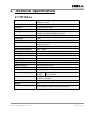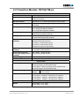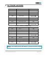
1
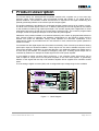
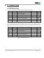
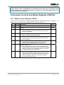
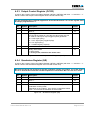
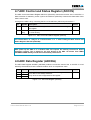
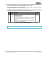
The Embedded I/O Company TIP102 Motion Controller with Incremental Encoder Interface Version 1.1 User Manual Issue 1.8 February 2007 D75102800 TEWS TECHNOLOGIES GmbH Am Bahnhof 7 Phone: +49-(0)4101-4058-0 25469 Halstenbek, Germany Fax: +49-(0)4101-4058-19 www.tews.com e-mail: [email protected] TEWS TECHNOLOGIES LLC 9190 Double Diamond Parkway, Suite 127, Reno, NV 89521, USA www.tews.com Phone: +1 (775) 850 5830 Fax: +1 (775) 201 0347 e-mail: [email protected] TIP102-1x One axis motion controller incremental encoder interface TIP102-2x Two axes motion controller incremental encoder interface TIP102-TM-10 Transition Module for TIP102-1x Isolated 24V digital I/O TIP102-TM-11 Transition Module for TIP102-1x Isolated 24V digital I/O, encoder This document contains information, which is proprietary to TEWS TECHNOLOGIES GmbH. Any reproduction without written permission is forbidden. TEWS TECHNOLOGIES GmbH has made any effort to ensure that this manual is accurate and complete. However TEWS TECHNOLOGIES GmbH reserves the right to change the product described in this document at any time without notice. TEWS TECHNOLOGIES GmbH is not liable for any damage arising out of the application or use of the device described herein. Style Conventions Hexadecimal characters are specified with prefix 0x, i.e. 0x029E (that means hexadecimal value 029E). TIP102-TM-12 Transition Module for TIP102-1x Isolated 24V digital I/O, encoder, analog out For signals on hardware products, an ‚Active Low’ is represented by the signal name with # following, i.e. IP_RESET#. TIP102-TM-13 Transition Module for TIP102-1x Isolated 24V digital I/O, encoder, analog in & out Access terms are described as: W Write Only TIP102-TM-20 R Read Only R/W Read/Write Transition Module for TIP102-2x Isolated 24V digital I/O TIP102-TM-21 R/C Read/Clear R/S Read/Set Transition Module for TIP102-2x Isolated 24V digital I/O, encoder 1994-2007 by TEWS TECHNOLOGIES GmbH TIP102-TM-22 All trademarks mentioned are property of their respective owners. Transition Module for TIP102-2x Isolated 24V digital I/O, encoder, analog out TIP102-TM-23 Transition Module for TIP102-2x Isolated 24V digital I/O, encoder, analog in & out TIP102 User Manual Issue 1.8 Page 2 of 31 Issue Description Date 1.0 First Issue April 1994 1.1 Extended December 1994 1.2 Technical Specification April 1996 1.3 General Revision October 2003 1.4 Add ID PROM contents for version 1.1 September 2004 1.5 Additional note for ADC conversion October 2004 1.6 More detailed description of the various I/O signals October 2005 1.7 New address TEWS LLC September 2006 1.8 Signal Polarity Clarification in Pin Assignment Tables February 2007 TIP102 User Manual Issue 1.8 Page 3 of 31 Table of Contents 1 2 PRODUCT DESCRIPTION........................................................................................... 6 TECHNICAL SPECIFICATION .................................................................................... 7 2.1 2.2 3 4 TIP102-xx .........................................................................................................................................7 Transition Module TIP102-TM-xx...................................................................................................8 ID PROM CONTENTS.................................................................................................. 9 IP ADDRESSING ....................................................................................................... 10 4.1 4.2 4.3 4.4 I/O Addressing...............................................................................................................................10 Input and Status Register (INPSR) ..............................................................................................11 Output Control Register (OUTCR)...............................................................................................13 Counter Data Register (CNTDA) ..................................................................................................13 4.4.1 Reading Counter Data........................................................................................................13 4.4.2 Writing Counter Data ..........................................................................................................13 4.5 Counter Control and Status Register (CNTCS)..........................................................................14 4.5.1 Master Control Register (MCR) ..........................................................................................14 4.5.2 Input Control Register (ICR) ...............................................................................................15 4.5.3 Output Control Register (OCCR)........................................................................................16 4.5.4 Quadrature Register (QR) ..................................................................................................16 4.5.5 Output Status Register (OSR) ............................................................................................17 4.6 DAC Data Register (DACDA)........................................................................................................17 4.7 ADC Control and Status Register (ADCCS) ...............................................................................18 4.8 ADC Data Register (ADCDA)........................................................................................................18 4.9 Configuration Control Register (CONCR)...................................................................................19 4.10 Interrupt Vector Register (INTVEC) .............................................................................................20 5 FUNCTIONAL DESCRIPTION ................................................................................... 21 5.1 5.2 6 PROGRAMMING HINTS ............................................................................................ 23 6.1 7 LS7166 Counter Chip....................................................................................................................23 6.1.1 Initialization .........................................................................................................................23 6.1.2 Reading actual counter data value .....................................................................................23 JUMPER CONFIGURATIONS ................................................................................... 25 7.1 7.2 8 Reference Logic ............................................................................................................................21 5.1.1 Reference Mode - without reference switch .......................................................................21 5.1.2 Reference Mode - with reference switch ............................................................................22 External Trigger Input...................................................................................................................22 TIP102-xx IP ...................................................................................................................................25 TIP102-TM-xx Transition Module.................................................................................................25 7.2.1 Trigger I/O Jumper Configuration .......................................................................................25 7.2.2 Encoder Input Jumper Configuration..................................................................................25 7.2.3 TIP102-TM-xx Jumper Layout ............................................................................................26 PIN ASSIGNMENT – I/O CONNECTOR .................................................................... 27 8.1 8.2 I/O Connection of TIP102-xx ........................................................................................................27 8.1.1 50 pin IP I/O Connector ......................................................................................................27 Transition Module I/O Connectors (TIP102-TM-xx) ...................................................................28 8.2.1 X101/X201 - DB9 female - Servo Amplifier Signals ...........................................................28 8.2.2 X102/X202 - DB15 male - Power and I/O Signals..............................................................29 8.2.3 X103/X203 - DB15 female - Encoder Signals ....................................................................31 TIP102 User Manual Issue 1.8 Page 4 of 31 Table of Figures FIGURE 1-1 : BLOCK DIAGRAM......................................................................................................................6 FIGURE 2-1 : TECHNICAL SPECIFICATION TIP102-XX................................................................................7 FIGURE 2-2 : TECHNICAL SPECIFICATION TIP102-TM-XX .........................................................................8 FIGURE 3-1 : TIP102 V1.0 - ID PROM CONTENTS ........................................................................................9 FIGURE 3-2 : TIP102 V1.1 - ID PROM CONTENTS ........................................................................................9 FIGURE 4-1 : REGISTER SET TIP102-1X .....................................................................................................10 FIGURE 4-2 : REGISTER SET TIP102-2X .....................................................................................................10 FIGURE 4-3 : INPUT AND STATUS REGISTER (INPSR) .............................................................................12 FIGURE 4-4 : OUTPUT CONTROL REGISTER (OUTCR) ............................................................................13 FIGURE 4-5 : COUNTER MASTER CONTROL REGISTER (MCR) ..............................................................14 FIGURE 4-6 : COUNTER INPUT CONTROL REGISTER (ICR) ....................................................................15 FIGURE 4-7 : COUNTER OUTPUT CONTROL REGISTER (OCCR)............................................................16 FIGURE 4-8 : QUADRATURE REGISTER (QR) ............................................................................................16 FIGURE 4-9 : OUTPUT STATUS REGISTER (OSR).....................................................................................17 FIGURE 4-10: DAC DATA REGISTER (DACDA) ...........................................................................................17 FIGURE 4-11: ADC CONTROL AND STATUS REGISTER (ADCCS) ...........................................................18 FIGURE 4-12: ADC DATA REGISTER (ADCDA) ...........................................................................................18 FIGURE 4-13: CONFIGURATION CONTROL REGISTER (CONCR)............................................................19 FIGURE 4-14: INTERRUPT VECTOR REGISTER (INTVEC)........................................................................20 FIGURE 5-1 : STATE DIAGRAM – REFERENCE WITH REFERENCE SWITCH .........................................22 FIGURE 7-1 : JUMPER J1 (J200) CONFIGURATION FOR TRIGGER INPUT AND OUTPUT .....................25 FIGURE 7-2 : JUMPER J1 (J200) CONFIGURATION FOR TRIGGER OUTPUT .........................................26 FIGURE 8-1 : 50 PIN IP I/O CONNECTOR TIP102-XX .................................................................................27 FIGURE 8-2 : X101/X201 - DB9 FEMALE - SERVO AMPLIFIER SIGNALS .................................................28 FIGURE 8-3 : X102/X202 - DB15 MALE - POWER AND I/O SIGNALS.........................................................30 FIGURE 8-4 : X103/X203 - DB15 FEMALE - ENCODER SIGNALS ..............................................................31 TIP102 User Manual Issue 1.8 Page 5 of 31 1 Product Description The TIP102 family are IndustryPack® compatible modules with complete one or two axes high precision motion control interfaces, using incremental encoder with RS422 or TTL signal level for position feedback. The transition module TIP102-TM-xx is required for the signal conditioning and optional galvanically isolation of the various input and output signals. The position feedback is provided by an incremental encoder interface and a 24 bit up/down counter. The level of the encoder signals can be TTL or RS422. Optionally the encoder signals can be isolated on the transition module by high speed optocoupler. The encoder signals pass a digital filter for noise suppression before they are fed into the counter and the reference logic. The counter is programmable for single, double and quadruple analysis of the encoder two phase signals. Calibration of the position feedback to an absolute reference point is done by programmable reference logic. Several modes of operation and hardware configurations for the reference switch and the encoder zero pulse are selectable. During normal operation the automatic recalibration of the measurement system is practicable with the “auto reference” mode, whenever the system passes the reference location. Two isolated 24V DC digital inputs have limit switch functionality. Each of these inputs drives a floating optocoupler output as hardware feedback. These outputs can be used to disable the power on the motor power amplifier, dependent on the actual direction. One additional isolated 24V digital input is for free use by the software, for example as emergency stop input. A floating optical output can be controlled by software, for example as enable signal for the motor power amplifier. A 16 bit digital to analog converter (DAC) produces a +/-10V controller output signal which can be used as speed or torque source for the power amplifier of the motor drive system. A galvanically isolation of this signal with the help of an isolation amplifier will be supplied as a transition module option. A 12 bit analog to digital converter (ADC) with a configurable input voltage range is also available. Figure 1-1 : Block Diagram TIP102 User Manual Issue 1.8 Page 6 of 31 2 Technical Specification 2.1 TIP102-xx Interface Single Size IndustryPack Logic Interface compliant to ANSI/VITA 4-1995 ID ROM Data Format I I/O Space Used without wait states Memory Space Not used Interrupts Interrupt 1 (IP signal INTREQ0#) for axis 1 Interrupt 2 (IP signal INTREQ1#) for axis 2 DMA Not supported Clock Rate 8 MHz Module Type Type I Number of Axes TIP102-1x: 1 axis TIP102-2x: 2 axes Encoder Interface Incremental encoder interface with 24 bit up/down counter Input Count Frequency Up to 1.2 MHz Analog Input 1 ADC per axis, 12 bit, 10µs, input voltage +/-10V Analog Input Overvoltage Protection up to 25Vpp Analog Output 1 DAC per axis, 16 bit, output voltage +/-10V Analog Output Current +/-5mA Digital Inputs 5 inputs per axis TTL level Digital Outputs 2 outputs per axis TTL level External Trigger TTL input and TTL output Interface Connector 50-conductor flat cable Power Requirements 50mA typical @ +5V DC Temperature Range Operating Storage MTBF TIP102-1x : 698000 h TIP102-2x : 561000 h Humidity 5 – 95 % non-condensing Weight 30 g Transition Module TIP102-TM-xx is required, provides signal conditioning and optional isolation of digital and analog I/O signals 0° C to +70 °C -45°C to +125°C Figure 2-1 : Technical Specification TIP102-xx TIP102 User Manual Issue 1.8 Page 7 of 31 2.2 Transition Module TIP102-TM-xx Board Data Size 1 VME slot (6U) Number of Axes 1 axis for TIP102-1x 2 axes for TIP102-2x Encoder Interface Signal level TTL or RS422 optional galvanically isolated Analog Input 1 input per axis, input voltage +/-10V optional isolated (ADC on TIP102) Analog Input Overvoltage Overvoltage protection up to 100Vpp with galvanic isolation up to 12Vpp without galvanic isolation Analog Output 1 output per axis, overvoltage +/-10V optional isolated (DAC device is located on TIP102) Analog Output Current +/-20mA with galvanically isolation +/-50mA without galvanically isolation Digital Inputs per Axis (isolated) General purpose input 24V DC Reference switch input 24V DC Limit switch 1 control input 24V DC Limit switch 2 control input 24V DC Encoder error input TTL (low active) Digital Outputs per Axis (isolated) Enable output 24V DC (+ “in position” LED indication) Digital Outputs directly driven from Inputs per Axis (isolated) Limit_Switch_1 Output 24V DC Limit_Switch_2 Output 24V DC External Trigger 1 isolated TTL I/O per axis (jumper selectable input or output) 24V Output Load Max. 1000 ohm Physical data Power Requirements TIP102-TM-1x : 100mA typical @ +5V DC (without load), <60mA typical @ ±12V DC (without load) TIP102-TM-2x : 180mA typical @ +5V DC (without load), <90mA typical @ ±12V DC (without load) Temperature Range Operating Storage MTBF TIP102-TM-10: 1271000 h, TIP102-TM-11: 759000 h TIP102-TM-12: 1091000 h, TIP102-TM-13: 644000 h TIP102-TM-20: 867000 h, TIP102-TM-21: 488000 h TIP102-TM-22: 785000 h, TIP102-TM-23: 436000 h Humidity 5 – 95 % non-condensing Weight TIP102-TM-1x : min. 150g TIP102-TM-2x : max. 250g 0° C to +70 °C -45°C to +125°C Figure 2-2 : Technical Specification TIP102-TM-xx TIP102 User Manual Issue 1.8 Page 8 of 31 3 ID PROM Contents Address Function Contents 0x01 ASCII ‘I’ 0x49 0x03 ASCII ‘P’ 0x50 0x05 ASCII ‘A’ 0x41 0x07 ASCII ‘C’ 0x43 0x09 Manufacturer ID 0xB3 0x0B Model Number 0x0D Revision 0x10 0x0F Reserved 0x00 0x11 Driver-ID Low - Byte 0x00 0x13 Driver-ID High - Byte 0x00 0x15 Number of bytes used 0x0C 0x17 CRC TIP102-1x: 0x0A TIP102-2x: 0x0B TIP102-1x: 0x3E TIP102-2x: 0x5F Figure 3-1 : TIP102 V1.0 - ID PROM Contents Address Function Contents 0x01 ASCII ‘I’ 0x49 0x03 ASCII ‘P’ 0x50 0x05 ASCII ‘A’ 0x41 0x07 ASCII ‘C’ 0x43 0x09 Manufacturer ID 0xB3 0x0B Model Number 0x0D Revision 0x11 0x0F Reserved 0x00 0x11 Driver-ID Low - Byte 0x00 0x13 Driver-ID High - Byte 0x00 0x15 Number of bytes used 0x0C 0x17 CRC TIP102-1x: 0x0A TIP102-2x: 0x0B TIP102-1x: 0x9E TIP102-2x: 0xFF Figure 3-2 : TIP102 V1.1 - ID PROM Contents TIP102 V1.1 uses an FPGA instead of a PLD. TIP102 V1.1 is 100% pin and function compatible with V1.0. TIP102 User Manual Issue 1.8 Page 9 of 31 4 IP Addressing 4.1 I/O Addressing The complete register set of the TIP102 is accessible in the I/O space of the IP. Address Symbol Description Size (Bit) Access 0x01 INPSR1 Input / Status Register 8 R/C 0x03 OUTCR1 Output Control Register 8 R/W 0x05 CNTDA1 Counter Data Register 8 R/W 0x07 CNTCS1 Counter Control / Status Register 8 R/W 0x08 DACDA1 DAC Data Register 16 W 0x0B ADCCS1 ADC Control / Status Register 8 R/W 0x0C ADCDA1 ADC Data Register 16 R 0x0F CONCR1 Configuration Control Register 8 W 0x3F INTVEC Interrupt Vector Register 8 R/W Figure 4-1 : Register Set TIP102-1x On the TIP102-2x two axes motion controller the second axis can be accessed through a second set of Control and Status Registers. Only the INTVEC Interrupt Vector Register is shared between both axes. Address Symbol Description Size (Bit) Access 0x21 INPSR2 Input / Status Register 8 R/C 0x23 OUTCR2 Output Control Register 8 R/W 0x25 CNTDA2 Counter Data Register 8 R/W 0x27 CNTCS2 Counter Control / Status Register 8 R/W 0x28 DACDA2 DAC Data Register 16 W 0x2B ADCCS2 ADC Control / Status Register 8 R/W 0x2C ADCDA2 ADC Data Register 16 R 0x2F CONCR2 Configuration Control Register 8 W Figure 4-2 : Register Set TIP102-2x TIP102 User Manual Issue 1.8 Page 10 of 31 4.2 Input and Status Register (INPSR) The Input and Status Register INPSR1 (INPSR2) holds the actual status of all digital input lines and the status of the internal control logic. Access Reset Value Interrupt Status 1 = corresponding axis has generated an interrupt request. It must be reset under software control by writing ‘1’ to this bit. Bit is automatically cleared with the IP_RESET signal. R/C 0 Refer. Done Status of Reference Logic, used to calibrate the counter to a reference position 1 = reference function, which was started with a corresponding command in the Configuration Control Register (CONCR1/CONCR2), has completed successfully or the external trigger event has occurred (see also chapter of “Configuration Control Register”). Flag must be cleared with corresponding writing to the CONCR1/CONCR2. This bit is automatically cleared with the IP_RESET signal. R/C 0 5 Encoder Error Latched Encoder Error Status 1= error in the timing of the encoder phase signals has occurred or the encoder itself has reported an error. The source of this flag is the error detection logic within the digital filter for the encoder phase signals or the input of the encoder signal ENC_ERROR. It must be reset under software control by writing ‘1’ to this bit. Bit is automatically cleared with the IP_RESET signal. R/C 0 4 General Input General Purpose Input 1 = input is active 0 = input is not active This status bit corresponds to the General_Purpose input (Pin 5) on the X102/202 connector of the TIP102-TM transition module. R 3 Trigger Input External Trigger Input 1 = trigger input is active 0 = trigger input is not active This bit reflects the state of the external Trigger output switch (Pins 6 & 14) on the X102/202 connector of the TIP102-TM transition module. The bidirectional Trigger I/O signal must be configured as input when this bit is going to be used. The transition module TIP102-TM-xx has one set of isolated trigger I/O signals, which are jumper configurable as trigger input or trigger output (see chapter “Trigger I/O Jumper Configuration”). R 2 Ref Switch Reference Input (could also be used as another general purpose input) R Bit Symbol Description 7 Interrupt Status 6 TIP102 User Manual Issue 1.8 Page 11 of 31 Bit Symbol Description Access Reset Value 1 = input is active 0 = input is not active This status bit corresponds to the Reference input (Pin 12) on the X102/202 connector of the TIP102-TM transition module. 1 High Limit High Limit Switch Control Input 1 = switch is activated 0 = switch is not activated This status bit corresponds to the Limit_Switch_2_Control input (Pin 4) on the X102/202 connector of the TIP102-TM transition module. R 0 Low Limit Low Limit Switch Control Input 1 = switch is activated 0 = switch is not activated This status bit corresponds to the Limit_Switch_1_Control input (Pin 11) on the X102/202 connector of the TIP102-TM transition module. R Figure 4-3 : Input and Status Register (INPSR) TIP102 User Manual Issue 1.8 Page 12 of 31 4.3 Output Control Register (OUTCR) The Output Control Register OUTCR1 (OUTCR2) controls the status of some output signals. Bit Symbol Description Access 7:2 Not used 1 Status LED Bit controls the status of a LED located on the transition module. It can be read and written by software. This bit is automatically cleared with the IP_RESET signal. R/W 0 Servo Amplifier Enable Bit controls the status of a floating optocoupler output which is normally connected to the enable input of the servo amplifier of the motor drive system. It can be read and written by software. This bit is automatically cleared with the IP_RESET signal. R/W Figure 4-4 : Output Control Register (OUTCR) 4.4 Counter Data Register (CNTDA) The Counter Data Register CNTDA1 (CNTDA2) is the data I/O port to the LS7166 counter chip. It is used to the read counter position or to write a preset value. Because the LS7166 is a 24 bit counter, and the Data Register is only 8 bit wide, each data transfer needs three read or write cycles in sequence. 4.4.1 Reading Counter Data The 24 bit data value of the counter can only be accessed through a 24 bit Output Latch (OL) internal the LS7166. The data is latched into the OL under software control by setting bit 1 in the counter MCR register to ’1’ (see chapter “Master Control Register”) or by an external hardware signal (see chapter “External Trigger Input”). After that the data can be read through the CNTDA1 (CNTDA2) in three cycles in sequence. The transfer is least significant byte first, most significant byte last. The access to the three data bytes within the Output Latch (OL) is controlled by an internal address pointer, which is automatically incremented with each read cycle. This pointer should be reset directly prior the three read cycles by setting bit 0 in the counter MCR register (see chapter “Master Control Register”). 4.4.2 Writing Counter Data The 24 bit counter can be loaded from a 24 bit Preset Register (PR) internal the LS7166. The preset data has to be written to the PR through the CNTDA1 (CNTDA2) in three cycles in sequence. The transfer is least significant byte first, most significant byte last. The data is then transferred to the counter under software control by setting bit 3 in the counter MCR register to ’1’ (see chapter “Master Control Register”), by the reference logic (see chapter “Reference Logic”) or by an external hardware signal (see chapter “External Trigger Input”). TIP102 User Manual Issue 1.8 Page 13 of 31 The access to the three data byte within the Output Latch (OL) is controlled by an internal address pointer, which is automatically incremented with each read cycle. This pointer should be reset directly prior the three read cycles by setting bit 0 in the counter MCR register (see chapter “Master Control Register”). 4.5 Counter Control and Status Register (CNTCS) 4.5.1 Master Control Register (MCR) A write to the Counter Control and Status Register CNTCS1 (CNTCS2) with bit 6 = ‘0’ and bit 7 = ‘0’ will be a write to the Master Control Register of the LS7166 counter chip. Bit Symbol Description Access 7 Write ‘0’ W 6 Write ‘0’ W 5 Master Reset 1 = perform a master reset on the LS7166 counter chip and put it into initial state W 4 Reset COMPT 1 = clear the compare toggle flag COMPT W 3 Transfer PR to CNTR 1 = transfer the previously loaded 24 bit data value into the counter (CNTR) W 2 Reset of CNTR, BWT, CYT, Set Sign Register 1 = set the counter (CNTR) data value to zero, clear the borrow and carry toggle flag and set the sign bit. W 1 Transfer CNTR to OL 1 = latch the current 24 bit value of the counter (CNTR) into the OL register of the LS7166 counter chip for subsequent read-out. This bit can be combined with bit 0 to reset the OL address pointer at the same time. W 0 Reset PR/OL address pointer 1 = reset the internal PR/OL address pointer of the LS7166 counter chip, which is used during reads and writes to the CNTDA1/CNTDA2 register to access the three bytes forming the 24 bit data word. W Figure 4-5 : Counter Master Control Register (MCR) TIP102 User Manual Issue 1.8 Page 14 of 31 4.5.2 Input Control Register (ICR) A write to the Counter Control and Status Register CNTCS1 (CNTCS2) with bit 6 = ‘1’ and bit 7 = ‘0’ will be a write to the Input Control Register of the LS7166 counter chip. Bit Symbol Description Access 7 Write ‘0’ W 6 Write ‘1’ W 5 Configuration LCTR/LLTC pin of the LS7166 1 = event will latch the actual counter data value into the OL register. 0 = event (reference or external trigger) will load the counter with the contents of the PR register. On the TIP102 this pin is controlled by the reference and external trigger logic (see chapter “Functional Description”). W 4 Configuration ABGT/RCTR Bit must always be set to ‘0’ for the operation of the TIP102-xx W 3 A/B Input Enable 1 = enable A and B counter inputs 0 = disable all counting functions For standard motion controller application of the TIP102 the counter should be always enabled. W 2 Decrement Counter 1 = decrement the counter data value by one W 1 Increment Counter 1 = increment the counter data value by one W 0 A/B Input Mode 1 = define A as count input and B as count direction input with B=’0’ for up and B=’1’ for down 0 = define A as up count input and B as down count input In a standard motion controller application the TIP102 will operate with an incremental encoder and the counter chip LS7166 programmed to quadrature mode by configuring the QR register (see chapter “Quadrature Register”). In this case the A/B input mode bit has no function. W Figure 4-6 : Counter Input Control Register (ICR) TIP102 User Manual Issue 1.8 Page 15 of 31 4.5.3 Output Control Register (OCCR) A write to the Counter Control and Status Register CNTCS1 (CNTCS2) with bit 6 = ‘0’ and bit 7 = ‘1’ will be a write to the Output Control Register of the LS7166 counter chip. For the standard motion controller application of the TIP102 the bits 1 to 3 of this register must be always programmed as ‘0’. Bit Symbol Description Access 7 Write ‘1’ W 6 Write ‘0’ W 5:4 Input Trigger mode On TIP102 the output pin 16 of the LS7166 counter chip can be used for interrupt or output trigger impulse generation. 00 = CY# signal (carry) 01 = CYT signal (carry toggle flip flop) 10 = CY signal (carry) 11 = COMP# signal (compare) W 3:1 Normal count mode W 0 Binary / BCD mode 1 = BCD mode 0 = binary mode, should be the normal case W Figure 4-7 : Counter Output Control Register (OCCR) 4.5.4 Quadrature Register (QR) A write to the Counter Control and Status Register CNTCS1 (CNTCS2) with bit 6 = ‘1’ and bit 7 = ‘1’ will be a write to the Quadrature Register of the LS7166 counter chip. Because the TIP102 was designed to decode quadrature signals of encoders, one of the modes X1, X2 or X4 must be selected for standard operation of the module. Bit 2 to 5 are don’t cares. Bit Symbol Description Access 7 Write ‘1’ W 6 Write ‘1’ W 5:2 Don’t care bits 1:0 Quadrature mode, will put the LS7166 counter chip in quadrature counting mode Depending on the mode X1, X2 or X4 the counter data values have 1, 2 or 4 times the resolution of the encoder. W Figure 4-8 : Quadrature Register (QR) TIP102 User Manual Issue 1.8 Page 16 of 31 4.5.5 Output Status Register (OSR) A read of the Counter Control and Status Register CNTCS1 (CNTCS2) will be a read of the Output Status Register of the LS7166 counter chip. Bit Symbol Description Access 7:5 Not used - 4 UP / DOWN - Count direction indicator in quadrature mode. 0 = when counting down 1 = when counting up R 3 Sign Bit 0 = when CNTR underflow 1 = when CNTR overflow R 2 Compare Toggle Flip-Flop, toggles every time CNTR equals PR. R 1 Carry Toggle Flip-Flop, toggles every time CNTR overflows generating a carry. R 0 Borrow Toggle Flip-Flop, toggles every time CNTR underflows generating a borrow. R Figure 4-9 : Output Status Register (OSR) 4.6 DAC Data Register (DACDA) The DAC Data Register DACDA1 (DACDA2) is the write only data register for the ±10V controller output signal of the TIP102. The 2’s complement value written into this register is converted to the corresponding output voltage with a range of ±10V. Bit Symbol Description 15 S 16 bit DAC data in 2’s complement Only 16 bit access is supported for this register. A read to this register will return random data. 14:0 Access W Figure 4-10: DAC Data Register (DACDA) TIP102 User Manual Issue 1.8 Page 17 of 31 4.7 ADC Control and Status Register (ADCCS) The ADC Control and Status Register ADCCS1 (ADCCS2) controls the function of the 12 bit ADC. A data conversion is started by a write cycle to the ADCCS1 (ADCCS2). However the data value of this write is a don’t care. As long as the ADC is busy converting the bit 0 of the ADCCS1 (ADCCS2) will read as ’1’. Bit Symbol Access These unused bits may be in a random state when reading this register. 7:1 0 Description ADC Busy ADC Busy 1 = ADC is busy R/W Figure 4-11: ADC Control and Status Register (ADCCS) The unused bits 1 to 7 may be in a random state ’0’ or ’1’ when reading the ADC Control and Status Register ADCCS1 (ADCCS2). After power up the ADC is in a random state and requires two dummy conversions before operating correctly. This is based on the chip design of the ADC. All drivers from TEWS TECHNOLOGIES already include these two dummy conversions. 4.8 ADC Data Register (ADCDA) The ADC Data Register ADCDA1 (ADCDA2) holds the conversion result of the 12 bit ADC. It is left shifted by the hardware, that the software reads a 16 bit 2’s complement value. Bit Symbol Description 15 Sign 12 bit ADC Data in 2’s complement, shifted to register bits 15:4. Bits 3:0 are always read as 0. Only 16 bit access is supported for this register. 14:4 3:0 Access R Figure 4-12: ADC Data Register (ADCDA) TIP102 User Manual Issue 1.8 Page 18 of 31 4.9 Configuration Control Register (CONCR) The Configuration Control Register CONCR1 (CONCR2) controls the operation mode of the reference logic, the encoder configuration and interrupt generation. Writing to this register will clear the reference done flag (bit 6) in the Input and Status Register INPSR1 (INPSR2). The unused bits 5 to 7 may be in a random state ’0’ or ’1’ when reading the Configuration Control Register CONCR1 (CONCR2). Bit Symbol Description Access 7:5 Not used 4 Interrupt Enable 1 = a transition on the CY output of the LS7166 counter chip will generate an interrupt. For more details see LS7166 data sheet, which is part of the TIP102-ED Engineering Documentation. W 3 Encoder Difference Signal 1 = enables the analysis of the differential phase signal of a RS422 encoder in the digital filter. In this mode broken encoder wire will be detected and the Encoder Error Status will be set in the Input and Status Register if such an error occurs. This function requires a transition module with the isolated encoder input option. This bit is automatically cleared with the IP_RESET signal. W 2 Auto Reference Enable 1 = enable This will automatically repeat the selected function of the reference logic and external trigger (bit 0 and bit 1). More information see chapter “Functional Description”. This bit is automatically cleared with the IP_RESET signal. W 1:0 Reference Mode 00 = None - reference logic is disabled 01 = Without reference switch - zero signal of the encoder will trigger the load counter input of the LS7166 counter chip. 10 = With reference switch - zero signal of the encoder is combined with the reference switch input to produce the load counter signal for the LS7166 counter chip. 11 = External trigger - external input signal will generate the load counter pulse to the LS7166 counter chip. More information see chapter “Reference Logic”. These bits will be cleared automatically, when the reference condition or external trigger occurs and bit 2 is not set. These bits are also automatically cleared with the IP_RESET signal. W Figure 4-13: Configuration Control Register (CONCR) TIP102 User Manual Issue 1.8 Page 19 of 31 4.10 Interrupt Vector Register (INTVEC) The Interrupt Vector Register INTVEC is a byte wide read/write register. It is shared between both axes, but both axes will create an individual interrupt. For an interrupt from axis # 1 bit 0 of the interrupt vector will read as ’0’, for an interrupt from axis #2 it will read as ’1’. If the Interrupt Vector Register is for example loaded with ’0x60’, axis # 1 will create an interrupt at vector ’0x60’ and axis # 2 will create an interrupt at vector ’0x61’. Bit Symbol Description Access 7:1 Interrupt Vector loaded by software R/W 0 Interrupt from Axes 1 or 2 1 = interrupt from axis 2 0 = interrupt from axis 1 Example: If this register loaded with 0x60, axis 1 will create an interrupt at vector 0x60 and axis 2 will create an interrupt at vector 0x61. Axis 1 is using the INTREQ0# and axis 2 is using INTREQ1# interrupt request line of the IP bus. R/W Figure 4-14: Interrupt Vector Register (INTVEC) Axis #1 is using the INTREQ0 and axis #2 is using the INTREQ1 interrupt request line of the IP bus. TIP102 User Manual Issue 1.8 Page 20 of 31 5 Functional Description 5.1 Reference Logic Due to the nature of measurement systems with incremental encoders the absolute position of the axes are not known when the system is powered up. The system has to run through a reference procedure to calibrate the measurement system, in that case the counter, with the absolute positions. The TIP102 IP has a reference logic, which allows several modes of operation for the reference procedure. The reference logic is generating a pulse to the load counter input of the LS7166 chip, when the reference condition occurs. This signal will either preset the counter with a value which was previously loaded into the Preset Register of the counter chip, or load the actual value of the counter to the Output Latch of the counter chip, depending on the configuration of the LCTR/LLTC bit of the Input Control Register (ICR). The desired operation mode of the reference logic is selected by programming the corresponding bits in the Configuration Control Register (CONCR). 5.1.1 Reference Mode - without reference switch In this mode the next occurrence of the zero (index) signal of the encoder is used as the source for the reference condition and therefore for the load counter signal. Because the incremental encoder will normally create a zero (index) pulse at each turn, this mode is only useful, if the absolute position of the next zero (index) pulse is known, or if there is only one such pulse in the operating range of the axis. TIP102 User Manual Issue 1.8 Page 21 of 31 5.1.2 Reference Mode - with reference switch This mode also uses the zero (index) signal of the encoder to generate the reference condition. But it takes an additional Reference Switch (which is an input to the TIP102) to select a single zero (index) signal. The reference condition in this mode is defined as the first zero (index) pulse of the encoder after a ’0’ to ’1’ transition of the reference switch, with the reference switch still in the ’1’ state. Figure 5-1 : State diagram – Reference with reference switch 5.2 External Trigger Input The TIP102 IP has a trigger input signal TRIGGER INPUT which can be used to latch the actual value of the counter or preload the counter at an external event. The Trigger Input is generating a pulse to the load counter input of the LS7166 chip, when the external trigger condition occurs. This signal will either preset the counter with a value which was previously loaded into the Preset Register of the counter chip, or load the actual value of the counter to the Output Latch of the counter chip, depending on the configuration of the LCTR/LLTC bit of the Input Control Register (ICR). The external trigger logic is activated by programming the corresponding bits in the Configuration Control Register (CONCR); see also description in chapter “Reference Mode”. The external trigger and the reference logic can not be used at the same time. The transition module TIP102-TM-xx has only one set of isolated TRIGGER I/O signals, which is jumper configurable as Trigger Input or Trigger Output (see also chapter “Trigger I/O Jumper Configuration”). TIP102 User Manual Issue 1.8 Page 22 of 31 6 Programming Hints 6.1 LS7166 Counter Chip 6.1.1 Initialization The LS7166 counter chip of the TIP102 requires some basic initialization, before it is able to decode the quadrature counting pulses of the incremental encoder. To do this the following data sequence has to be loaded into the CNTCS1 (CNTCS2) Counter Control and Status Register: • write 0x20 to CNTCS1 (CNTCS2) select the counter MCR register, perform a master reset on the LS7166 counter chip • write 0x68 to CNTCS1 (CNTCS2) select the counter ICR register, enable data inputs A/B, configure pin 3 as counter load input (required for the reference logic) • write 0xB0 to CNTCS1 (CNTCS2) select the counter OCCR register, configure pin 16 as compare result output (required for generation of interrupts at defined counter data values) • write 0xC1, 0xC2 or 0xc3 to CNTCS1 (CNTCS2) select the counter QR register, enable quadrature decoding mode X1, X2 or X4 After this initialization the counter will begin decoding the encoder quadrature signals. 6.1.2 Reading actual counter data value The LS7166 has a 24 bit up/down counter. However the data path to the LS7166 is only 8 bit wide. To read the 24 bit counter data value (8 bit at a time), following sequence must be programmed: • write 0x03 to CNTCS1 (CNTCS2) select the counter MCR register, latch the actual counter data value into the Output Latch (OL), reset the OL address pointer • read CNTDA1 (CNTDA2) read data byte 0 (LSB), increment OL address pointer • read CNTDA1 (CNTDA2) read data byte 1, increment OL address pointer • read CNTDA1 (CNTDA2) TIP102 User Manual Issue 1.8 Page 23 of 31 If the data bytes 0 to 2 are assembled into a 32 bit word the sign bit of the counter has to be extended for further processing, which means bit 7 of data byte 2 into the upper 8 bits of the 32 bit word. TIP102 User Manual Issue 1.8 Page 24 of 31 7 Jumper Configurations 7.1 TIP102-xx IP There are no jumpers to configure on the TIP102-xx IP. Do never place any jumper on the 10 pin connector block of the TIP102-xx IP. This block is used only for manufacturing and testing purpose. 7.2 TIP102-TM-xx Transition Module 7.2.1 Trigger I/O Jumper Configuration The Trigger I/O signals at connector X102 (X202) of the transition module must be configured to input or output by the jumper J1 (J200) at the transition module. Figure 7-1 : Jumper J1 (J200) configuration for trigger input and output 7.2.2 Encoder Input Jumper Configuration The TIP102-TM-10 and TIP102-TM-20 transition modules have jumpers to enable or disable the PHASE_A, PHASE_B and INDEX encoder inputs. If the encoder provides the PHASE_A, PHASE_B and INDEX signals the jumper J2, J3 and J4 (J201, J202 and J203) must be jumpered between pin 1 and 2. If the encoder does not provide the PHASE_A, PHASE_B and INDEX signals the jumper J2, J3 and J4 (J201, J202 and J203) must be jumpered between pin 2 and 3. TIP102 User Manual Issue 1.8 Page 25 of 31 7.2.3 TIP102-TM-xx Jumper Layout Figure 7-2 : Jumper J1 (J200) configuration for trigger output The jumpers J2, J3 and J4 (J201, J202 and J203) are only present at the TIP102-TM-10 (TIP102TM-20) transition module. TIP102 User Manual Issue 1.8 Page 26 of 31 8 Pin Assignment – I/O Connector 8.1 I/O Connection of TIP102-xx 8.1.1 50 pin IP I/O Connector Pin Function Pin Function 1 +5V VCC 26 ENC_PHASE_B_AXIS_1+ (TTL Input) 2 +5V VCC 27 ENC_PHASE_A_AXIS_1- (TTL Input) 3 GND 28 ENC_PHASE_A_AXIS_1+ (TTL Input) 4 GND 29 Status_LED_Axis_2 (TTL output) 5 +12V 30 Servo_Amp_Enable_Axis_2 (TTL output) 6 -12V 31 GND 7 Status_LED_Axis_1 (TTL output) 32 DAC_Output_Axis_2 (+/-10V) 8 Servo_Amp_Enable_Axis_1 (TTL output) 33 DAC_GND_Axis_2 9 GND 34 ADC_Input_Axis_2 (+/-10V) 10 DAC_Output_Axis_1 (+/-10V) 35 ADC_GND 11 DAC_GND_Axis_1 36 GND 12 ADC_Input_Axis_1 (+/-10V) 37 Trigger_Input_Axis_2# (TTL input) 13 ADC_GND 38 Trigger_Output_Axis_2# (TTL output) 14 GND 39 General_Input_Axis_2# (TTL input) 15 Trigger_Input_Axis_1# (TTL input) 40 Reference_Switch_Axis_2# (TTL input) 16 Trigger_Output_Axis_1# (TTL output) 41 High_Limit_Switch_Axis_2# (TTL input) 17 General_Input_Axis_1# (TTL input) 42 Low_Limit_Switch_Axis_2# (TTL input) 18 Reference_Switch_Axis_1# (TTL input) 43 Encoder_Error_Axis_2# (TTL input) 19 High_Limit_Switch_Axis_1# (TTL input) 44 NC 20 Low_Limit_Switch_Axis_1# (TTL input) 45 ENC_INDEX_AXIS_2- (TTL Input) 21 Encoder_Error_Axis_1# (TTL input) 46 ENC_INDEX_AXIS_2+ (TTL Input) 22 NC 47 ENC_PHASE_B_AXIS_2- (TTL Input) 23 ENC_INDEX_AXIS_1- (TTL Input) 48 ENC_PHASE_B_AXIS_2+ (TTL Input) 24 ENC_INDEX_AXIS_1+ (TTL Input) 49 ENC_PHASE_A_AXIS_2- (TTL Input) 25 ENC_PHASE_B_AXIS_1- (TTL Input) 50 ENC_PHASE_A_AXIS_2+ (TTL Input) Figure 8-1 : 50 pin IP I/O Connector TIP102-xx TIP102 User Manual Issue 1.8 Page 27 of 31 8.2 Transition Module I/O Connectors (TIP102-TM-xx) 8.2.1 X101/X201 - DB9 female - Servo Amplifier Signals Signal Level Pin Function 1 Current_Limit_Switch_1+ Current Limit Switch 1 (floating optocoupler output transistor collector pin) See also pin 6. The switch state is controlled by the matching control input on X102/202 (Pin 11). 2 Current_Limit_Switch_2+ Current Limit Switch 2 (floating optocoupler output transistor collector pin) See also pin 7 The switch state is controlled by the matching control input on X102/202 (Pin 4). 3 Enable_Switch+ Enable Switch (floating optocoupler output transistor collector pin) See also pin 8. The switch state is controlled by OUTCR register bit 0. 4 Shield 5 DAC_GND Analog output ground reference See also pin 9. 6 Current_Limit_Switch _1- Current Limit Switch 1 (floating optocoupler output transistor emitter pin) See also pin 1. The switch state is controlled by the matching control input on X102/202 (Pin 11). 7 Current_Limit_Switch _2- Current Limit Switch 1 (floating optocoupler output transistor emitter pin) See also pin 2. The switch state is controlled by the matching control input on X102/202 (Pin 4). 8 Enable_Switch- Enable Switch (floating optocoupler output transistor emitter pin) See also pin 3. The switch state is controlled by OUTCR register bit 0. 9 DAC_Output +/-10V Comment Analog output See also pin 5. Figure 8-2 : X101/X201 - DB9 female - Servo Amplifier Signals TIP102 User Manual Issue 1.8 Page 28 of 31 8.2.2 X102/X202 - DB15 male - Power and I/O Signals Pin Signal 1 ENC_VCC Encoder power supply (source) Direct on-board connection to X103/203 pins 1 & 9 Connect to power supply. 2 ENC_VCC_SENSE Encoder power supply sense (source) Direct on-board connection to X103/203 pin 3 Connect to power supply sense input (if applicable). 3 Shield 4 Limit_Switch_2_Control Input 24V 24V control input to activate the Current_Limit_Switch_2 on X101/201 State readable in INPSR register bit 1 5 General_Purpose Input 24V General purpose 24V input State readable in INPSR register bit 4 6 Trigger_I/O+ Input Configuration: TTL Bidirectional Trigger I/O signal, direction is configured by jumper See also pin 14. TTL Input configuration : Anode of photodiode When configured as input, the status of this input is reflected by INSPR register bit 3. Output switch configuration : Floating optocoupler output transistor collector pin 7 Shield 8 ADC_GND Analog input ground reference See also pin 15. 9 ENC_GND Encoder power supply ground (source) Direct on-board connection to X103/203 pins 2 & 10 Connect to power supply ground. 10 ENC_GND_SENSE Encoder power supply sense ground (source) Direct on-board connection to X103/203 pin 11 Connect to power supply sense ground input (if applicable). 11 Limit_Switch_1_Control Input 24V 24V control input to activate the Current_Limit_Switch_1 on X101/201 State readable in INPSR register bit 0 12 Reference Input 24V Reference 24V Input State readable in INPSR register bit 2 TIP102 User Manual Issue 1.8 Level Comment Page 29 of 31 Pin Signal Level Comment 13 Common Return of Input Signals 24V Common Return Common Return Signal of the following 24V Inputs : General Purpose Input 1 (Pin 12) General Purpose Input 2 (Pin 5) Limit_Switch_1_Control_Input (Pin 11) Limit_Switch_2_Control_Input (Pin 4) 14 Trigger_I/O- Input Configuration: TTL Bidirectional Trigger I/O signal Direction is configured by jumper. See also pin 6. TTL Input configuration: Anode of photodiode When configured as input, the status of this input is reflected by INSPR register bit 3. Output switch configuration : Floating optocoupler output transistor collector pin 15 ADC Input +/-10V Analog Input See also Pin 8. Figure 8-3 : X102/X202 - DB15 male - Power and I/O Signals TIP102 User Manual Issue 1.8 Page 30 of 31 8.2.3 X103/X203 - DB15 female - Encoder Signals Pin Signal 1 ENC_VCC Level Encoder Power Supply Connect to Encoder Comment 2 ENC_GND Encoder Power Supply Ground Connect to Encoder 3 ENC_VCC_SENSE Encoder Power Supply Sense Connect to Encoder (if applicable) 4 NC 5 INDEX- TTL or RS422 - Encoder Index Line Connect to Encoder 6 PHASE_B- TTL or RS422 - Encoder Phase B Line Connect to Encoder 7 PHASE_A- TTL or RS422 - Encoder Phase A Line Connect to Encoder 8 Shield 9 ENC_VCC Encoder Power Supply. Connect to Encoder 10 ENC_GND Encoder Power Supply Ground Connect to Encoder 11 ENC_GND_SENSE Encoder Power Supply Sense Ground Connect to Encoder (if applicable) 12 ENC_ERROR# TTL Encoder Error Input Connect to Encoder (if applicable) State readable in INPSR register bit 5 13 INDEX+ TTL or RS422+ Encoder Index Line Connect to Encoder 14 PHASE_B+ TTL or RS422+ Encoder Phase B Line Connect to Encoder 15 PHASE_A+ TTL or RS422 + Encoder Phase A Line Connect to Encoder Figure 8-4 : X103/X203 - DB15 female - Encoder Signals TIP102 User Manual Issue 1.8 Page 31 of 31