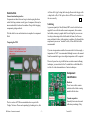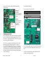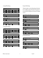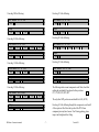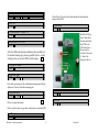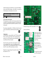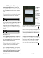
1
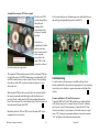
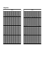
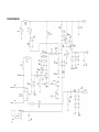
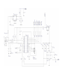
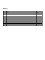
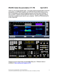
The Radio-Kits “Hunter”
SDR receiver and Panadapter
Construction and user manual
Author - Steve Drury G6ALU
List of contents
Section
1. Features
2. Specifications
3. Introduction
4. Construction
5. General construction practice
6. Soldering
7. Component identification
8. Component placement
9. Assembling to case
10. Commissioning
11. In use
12. Fault finding
13. Safety considerations
14. Circuit description
15. Voltage tables
16. Circuit diagram
17. PCB overlay
18. Change log
RK Hunter Construction manual
Page no.
2
2
2
3
3
3
3
4
11
12
14
14
15
15
17
18-20
21
22
-1-
Version R1.1
Introduction
Features
•
•
•
•
•
Monitors a wide frequency span
Adds a Panadapter function to a commercial transceiver without
internal modification
Tunes transceiver to selected frequency via CAT control1
Powered from USB
Kit includes a high quality PCB, all components, case and solder
Hunter translates a section of the HF band to a frequency suitable for
processing by an external sound card and PC; for a sound-card
sampling at 192kHz the displayed bandwidth approaches 190kHz,
similarly bandwidths of 90kHz for 96kHz sample frequency and
45kHz for a 48kHz sample frequency can be expected. SDR receiver
performance is heavily reliant on the sample rate and dynamic range
of the sound card used; many PCs (laptops included) now incorporate
a 24bit 96kHz sound card, this specification is recommended as a
minimum. If the PC doesn’t have a suitable sound card second user
parts are inexpensive when sourced from eBay.
Typical Specifications
Operating Frequency
Single tone dynamic range
Sensitivity
Maximum power handling
-
RK-Hunter is a HF band SDR receiver based on the now classic QSD
(quadrature sampling detector) technology first introduced to the
amateur community by Gerald Youngblood K5SDR in the
FlexradioTM and later by Tony Parks KB9YIG in the softrock series of
receivers. In addition, the Hunter also has circuitry to enable its use as
a panoramic adapter; the receiver can be placed “inline” between
antenna and transceiver and incorporates a changeover relay allowing
antenna switching between the SDR receiver and the connected
transceiver.
2.5 – 30MHz 2
> 110dB dynamic range3
Noise floor -137dBm3
120W
1 Transceiver requires CAT control from PC
2 Determined by lower frequency of Si570, 1 - 30MHz typically
3 Parameters dependent on sound card specifications
Frequency control and power for Hunter is provided by a single USB
connection with the PC, current consumption is about 150mA so if a
separate USB hub is used it will need to be of the powered type.
RF sensing is provided to automate the change over, this can be
overridden with a push switch. If transmit power is sensed the relay
will remain switched to the transceiver until the manual switch is
depressed then released; this is to stop repeated relay operation and
possible damage to the relay contacts. RF power has to be present
before the relay is switched so “hot” switching is inevitable.
RK Hunter Construction manual
-2-
Version R1.1
Construction
General construction practice
Components are taken from one bag at a time keeping the others
sealed. Each bag contains several types of component, this may be
unconventional but it reduces the number of bags whilst stopping
components getting confused.
Tick the check box as each instruction is completed or component
fitted.
Preparing the PCB
will leave little “pips” along the front edge. Remove the the pips with
a sharp knife or file, if left in place the two PCBs won't assemble into
the case correctly.
Soldering
A generous quantity of thin (0.46mm) SMT rework solder has been
supplied for use with the surface mount components, this contains
lead which, contrary to popular belief is not illegal for your own use.
As always when using solder don't breathe the fumes, the flux can
cause problems for those with respiratory conditions. For through hole
components you can use “standard” solder, 0.7mm 60/40 tin lead is
recommended.
If you use a temperature controlled iron ensure that it is hot enough, a
temperature of 360°C is recommended although to remove the enamel
from the enamelled copper wire a higher temperature will be required.
There isn't space here to give full tuition on surface mount soldering
techniques, you are referred to the You-tube links on the Radio-Kits
web site for video demonstrations of various techniques.
Component
identification
Resistors
These have a white ceramic
substrate with a black covering
marked with the value.
The two sections of PCB were manufactured as one part with
“bridges” between. These need separating by breaking in two, this
RK Hunter Construction manual
-3-
Ceramic capacitors
Generally brown in colour and
without any markings, if they
Version R1.1
become mixed it won't be possible to identify them without a
capacitance meter.
From Bag1 fit the following:
Note – solder tabs of U2 and U3 to PCB
Diodes and
transistors
Diodes and transistors
use the same three leg
package.
MCP1824T Marked “1824ADJ”
U2
MCP1702T Marked “HG****”
U3
Inductors
Inductors have plastic
bodies, the colour is
dependent on
manufacturer.
Component placement
First to be fitted are the surface mounted integrated circuits, these are
easiest to fit without other components getting in the way. IC's are
static sensitive so take sensible precautions. IE don't work on a nylon
carpet and use an earthed soldering iron.
First “tin” one corner pad with a little solder then sit the IC on this
carefully aligning all pins and ensuring the device orientation is
correct. Whilst still holding the chip with tweezers (or by applying
light pressure on top of the IC) apply the soldering iron to that single
pad. If all the pins aren't perfectly aligned with the pads then reheat
the joint and realign the chip, when you are happy that the alignment
is correct solder all pins.
RK Hunter Construction manual
-4-
Pin 1 of U5 isn't explicitly marked, if you look VERY carefully one
side of the device has a larger chamfer than the other, this is pin 1
side.
It may be easier to use the photo as reference taking note of the
orientation of the writing on the chip.
Version R1.1
LT6231 Marked “6231”
U5
82pF
C7
Pin 1 of U6 is marked with a dot
BAV99 Marked “A7”
D5
D10
74VHC74 Marked “74VHC74”
C54
D6
D7
D8
R32
R33
D9
U6
330nH Marked “331”
L2
L12
Pin one end of U7 is identified with a printed bar, note this IC is
mounted in the opposite direction to U5.
From bag 4 fit the following:
SN74CBT3253 Marked “CBT3253C”
68R Marked “680”
R4
R5
R53
R54
U7
From bag 2 fit the following:
BAP64-05 or BAP65-05 Marked “5KW” or “7KW”
47k Marked “4702” or “473”
R1
R10
R24
10nF
C5
C18
C6
C26
C13
D11
D16
C15
0.1uF
C8
C20
C31
C49
C57
C68
C73
C16
BZX84 C3V6 Marked “WB2”
D3
D4
10uH Marked “100”
L1
L9
From bag 3 fit the following:
D13
D14
D15
C10
C21
C32
C50
C59
C69
C74
C11
C22
C33
C52
C60
C70
C14
C28
C34
C53
C62
C71
C17
C30
C42
C55
C65
C72
470nH Marked “R47”
L3
L13
15k Marked “153” or “1502”
R3
R7
RK Hunter Construction manual
D12
-5-
Version R1.1
From bag 5 fit the following:
From bag 7 fit the following:
100R Marked “101” or “1000”
R6
R11
R14
R28
R29
R50
The fuse looks similar to a resistor (white marking on a black surface)
but is in a slightly larger package (1206). Ensure this component is in
the correct place before soldering as it will be destroyed if you attempt
to move it.
R15
R52
R19
4.7uF
C9
200mA 1206 Fuse Marked “C”
R9
BC847B Marked “1FN”
240R Marked “241” or “2400”
R55
Q1
1uH
Marked “1R0”
L4
L10
22pF
C23
L14
From bag 6 fit the following:
1k Marked “102” or “1001”
R8
R18
R22
R46
R48
MMBFJ310 Marked “GT”
Q5
R31
R43
4.7uH Marked “4R7”
L6
L11
1uF
C12
C43
C19
C48
C24
C51
C35
Q3
2.2uH Marked “2R2”
L5
L8
RK Hunter Construction manual
L16
From bag 8 fit the following:
C36
1M Marked “105” or “1004”
R12
BC857B Marked “3F”
Q2
C25
Q4
180pF
C37
L15
C46
C61
680nH Marked “681”
L7
-6-
Version R1.1
From bag 9 fit the following:
From bag 13 fit the following:
3k3 Marked “332” or “3301”
R34
R37
2k2 Marked “222” or “2201”
R13
390pF
C38
C56
220pF
C44
C63
From bag 14 fit the following:
From bag 10 fit the following:
10k Marked “103” or “1002”
R16
R17
R23
820pF
C39
C45
R40
4k7 Marked “472” or “4701”
R35
R36
R38
R41
680pF
C47
C64
From bag 15 fit the following:
From bag 11 fit the following:
470R Marked “471” or “4700”
R20
R26
R56
22R Marked “220” or “22R0”
1500pF
C40
1200pF
C58
R44
C66
From bag 12 fit the following:
10R Marked “100” or 10R0”
R30
R42
R45
R51
2700pF
C41
R47
The following surface mount components aren't fitted, check that
nothing has accidentally been placed in their positions:
C27, C29, R2, R21, R25, R27
R49
The only other SMT position vacant should be for U4 (Si570).
From bag 16 fit the following through hole components, note that all
of these parts are fitted from the top-side of the PCB. Some
component pins may have become “bent” during packing, please
inspect and straighten before fitting:
C67
RK Hunter Construction manual
R39
-7-
Version R1.1
220UF 10V
C1
C3
Fit the 28 pin IC socket so the notch matches the notch position
marked on the PCB.
C4
47UF 10V
C2
28 pin Socket
U1
1A wire ended fuse Marked “1A”
F1
Bend the LED legs
about 10mm from
the body and solder
into PCB so the
LED centre line is
the same as the
switches. The anode
(+) lead is the
longest of the two.
Relay Marked ”G5V-2 5DC”
RLY1
After the USB socket has been soldered in place carefully cut
the outside retaining tag as short as possible, this is to avoid it
shorting to the case once the PCB is slid into place.
USB type “B” socket
SKT1
3.5mm Jack socket
SKT2
SKT3
First solder just one pin of the switch and check alignment with the
silkscreen, if correct solder the remaining pins.
Red LED
D1
2 Pole push switch
SW1
SW2
Green LED
D2
Fit the two push switch caps.
Fit the crystal so there is a gap about 1mm between crystal and PCB.
16MHz Crystal
XTAL1
RK Hunter Construction manual
-8-
Version R1.1
Trim the
remaining 4
wires to about
4 cm long and
tin just the end
of the wire.
Using a
multimeter set
to read
continuity
identify the
start and end of
each wire, we
will call one
wire “A” and
the other wire
“B”. Twist the
end of wire
“A” with the
start of wire
“B” which will
form a centre
tap.
Winding T1
T1 uses a balun core and has a 5 turn primary winding with a bifilar
wound 3 turn secondary.
Cut a piece of 36 SWG enamelled copper wire about 30cm long and
fold it in half, squeeze the loop at the fold so it is more suitable for
passing through the core.
Thread the wire through one of the holes in the core leaving about
5cm of wire remaining then thread the long length through the other
hole – this is one complete “turn”.
Wind another 2 complete turns through
the core making a total of 3.
Cut another piece of 36 SWG wire
about 20cm long but do not fold it.
Pass the wire into the core from the
other side and wind on 5 complete
turns, this will result in a transformer
with 4 wires coming out of one side
and 2 from the other similar to the
photo.
Trim the 2 wires to about 2 cm and tin
along their length with a hot iron and
solder. If hot enough the molten solder
will break down the enamel and tin the
copper beneath, if your iron isn't hot enough it may be necessary to
scrape the wire prior to tinning, experiment with a spare piece first.
RK Hunter Construction manual
-9-
Tin the three
wires (one
being two
twisted
together) then confirm continuity between all three wires with a
multimeter.
Version R1.1
Install the transformer into the PCB, the core may touch the PCB and
can be secured with silicon adhesive, nail varnish or a very small drop
of hot melt glue once the complete receiver is tested.
BN43-2402 core Primary 5T, secondary 3+3T (bifilar
wound) using 36 SWG ECW
T1
Test for short circuits on input
With a digital meter switched to the resistance range measure between
one end of F1 (1 amp axial fuse) and ground – the ground connection
can be taken from the USB socket shield. Connect black (-Ve) meter
lead to ground.
Measure the voltage on TP3V3, this should be 3.3 ± 0.1V.
The resistance reading should be > 100k Ohms, if not look for a short
circuit or other fault between the USB socket and regulators U2 and
U3.
Voltage checks
Set the multimeter to a range suitable to read 5V DC and connect the
black (-Ve) lead to ground, it may be best to temporarily solder a
ground wire to one of the antenna connector ground pads to allow
easy attachment of the meter clip-lead.
Ensure the work area is clear of any stray components or metallic
objects and that the PCB is resting on an insulating surface then
connect the PCB to a PC using an appropriate USB lead – it is normal
for the PC to detect a USB source and report it as faulty.
Measure the two supply voltages; first measure the voltage on TP4V6,
this should be 4.6 ± 0.1V.
RK Hunter Construction manual
- 10 -
Remove the USB lead.
If either of the voltages are
incorrect diagnose the cause
before continuing as the
expensive Si570 will be
destroyed with an incorrect
supply voltage.
Fit the Si570 device in
position U4, this device is
packed in a separate bag
along with the other surface
mount parts.
First apply solder to one pad
only, whilst remelting the
Version R1.1
solder place the Si570 squarely and centrally between all pads – note
that the solder pads are underneath the device with only a small
witness up the side, use this witness as an indicator to centralise the
chip. Pin one is indicated by a dot on PCB and device, see photo for
details.
With a large drill
bit carefully
countersink the
holes for the
SO239 mounting
screws from the
outside of the end
plate, use a screw
to judge the
correct depth.
When you are sure the device is correctly orientated solder remaining
7 pads, ensure the witnesses are also soldered – refer to photo.
Si570
U4
Fit U1 to it's socket. Pin one end of the chip is marked by a “notch” on
the PCB and by a “dot” on the chip. The pins may need bending
inwards slightly to align with the socket, this is easily achieved by
carefully pressing all pins (on one side of the chip at a time) against a
flat surface.
To cut the square
hole for the USB
socket first drill a series of small holes and then join with a modelling
knife; take care not to cut yourself with the sharp knife!
Trial fit the front and rear panels, if all is OK permanently fit the front
panel to the aluminium extrusion as the front panel decal covers the
fixing screws, access for maintenance can be made by removing the
rear panel screws.
ATmega8A
U1
Assembling to case
The case front and rear will need drilling to accept the connectors and
buttons etc. Print the drilling template using Adobe reader TM; note
that “Page scaling” should be set to “None”. When printed measure
the scales to ensure they have printed accurately.
The drilling templates can be fitted to the inside of the end panels
using double sided sticky tape or a non-permanent adhesive.
From the Radio-Kits website download and print the front and rear
panel decals; remember to print with scaling set to “none”. Cover with
plastic film and use double side adhesive tape to fix to the panels.
Note that large holes have been made for the line out and PTT
sockets, this is to allow the plug to fit right down to the panel.
First drill the round holes to the indicated size, its best to work up in
drill size starting with perhaps a 2mm drill. The drill can be centred by
first applying a little pressure before allowing the drill bit to turn, this
causes an indent in the plastic which helps to locate the drill bit.
RK Hunter Construction manual
- 11 -
Version R1.1
Assemble the connector PCB to rear panel
Pass the two SO239
sockets through from
the inside and
securing with 8
countersunk screws,
shake proof washers
and nuts.
Cut two more short pieces of tinned copper wire and solder between
the earth tags and ground pads provided on the PCB.
Note that two
terminal tags fit under
the the lower outer
nuts, these are used to
make a ground
connection to the
main PCB . Fit the
connectors so the cut
out in the centre pin is uppermost.
The connector PCB assembly can now be fitted to the main PCB; first
cut and solder pieces of 20SWG tinned copper wire through the ANT
and TRX connector holes so there is about 15mm of wire protruding
from the top of the PCB, crop the wire under the board so it wont
short to the case.
Slide the main PCB into the lower slot of the case extrusion then fit
the connector assembly and hold in place with four black screws
provided. Check to make sure the PCB isn't protruding through the
front of the extrusion, if it is check that the “pips” have been removed
from the break off areas of the PCB.
Bend then solder the ANT and TRX wires to the inner SO239 pins
cropping the wire as necessary.
RK Hunter Construction manual
- 12 -
Commissioning
To test the radio its first necessary to install the software, if not
already installed follow the instructions appropriate for your operating
system; they can be found in a separate document on the Radio-Kits
website.
Connect up Hunter to PC and the transceiver
Connect the SDR to PC with USB lead and use an audio lead fitted
with 3.5mm stereo jacks to connect between “Line out” on Hunter
and “Line in” on the PC audio interface. Connect the SO239 “ant”
connector on Hunter to your antenna or if used the transceiver input
on an ATU, if using as a panoramic adapter to a transceiver connect
“Trx” on Hunter to the transceiver antenna socket.
Version R1.1
Hunter has provision for the antenna change over relay to be switched
via a transceiver PTT input, if this facility is used Hunter will
automatically switch to the transceiver as soon as the PTT is pressed.
To make use of this feature a lead is required fitted with a 3.5mm jack
plug (stereo or mono) Hunter end and on the other end a suitable
connector for the transceiver.
This calibration
should result in an
initial frequency
accuracy within
1.5ppm but can be
adjusted later
using “Calibrate
B” with reference
to a known signal
source (WWV
etc).
For the transceiver to follow the frequency tuned by Hunter, CAT
control will also need to be set up between the transceiver and PC;
integration between CAT and HDSDR is by a program called
“Omnirig”, which is free-ware.
With software
correctly installed
and running Hunter
should be identified
as a USB device.
This can be
confirmed by
clicking on the
small ExtIO icon
from within
HDSDR; this will
activate the
PE0FKO Softrock
Configuration tool.
In the bottom left hand corner is an activity indicator which will turn
green if Hunter has been identified.
Check the function of the antenna switching circuit
Connect an SWR or power meter to the “Ant” connector and
terminate this with a dummy load. Connect a HF transceiver to the
“TRX” connector and power Hunter via a PC.
Tune the transceiver to the 10M band and using low power (1 – 5
Watts) confirm Hunter senses the RF and switches the antenna to the
transceiver, this can be confirmed by the RED TRX LED lighting and
power being observed on the SWR / power meter. Note the SDR-TRX
switch will have to be pressed in and then out again to switch the
antenna back to SDR .
An unused microcontroller will need to interrogate the Si570 to
calculate the internal crystal frequency, to do this switch to the
“Calibrate” tab and under the heading “Calibrate A” click the calibrate
button. Note that the crystal frequency is different for every Si570.
RK Hunter Construction manual
- 13 -
Version R1.1
In Use
Fault finding
Hunter only has two physical controls:
Most faults are due to poor soldered connections or components
misplaced, it is very rare to be supplied with a faulty component.
Before making any measurements look carefully for any poor soldered
joints, short circuits or incorrectly fitted components.
SDR-TRX
Pressing this button will switch the antenna to the attached
transceiver, this should be used before transmitting; Hunter has RF
sensing which will switch the antenna to the transceiver automatically
but this shouldn't be relied on as for a short period the transceiver will
not be loaded. To avoid this happening repeatedly, the switching
circuit latches in the transmit mode; this can be released by depressing
and then releasing the SDR-TRX switch.
Attenuator
A 20dB attenuator is activated when the switch switch is pressed in,
this can help stop overloading when using large antennae or from very
strong signals; the switch should be left out if not required.
Should fault finding be necessary a table of voltages is given below,
voltages were measured with the LPF switched to 4-8MHz – tuned
frequency 7.1MHz. There are two tables provided, one in SDR mode
and the other with the SDR-TRX switch depressed.
It is possible for
the EEPROM data
within the
microcontroller to
become corrupted,
this can lead to
wrong or no
control of the
Si570 device. Use
the Softrock
Configuration tool
to return to the
default settings.
Select the Si570
tab and click on the “Factory default” button, calibration data will be
wiped so “Calibrate A” will need to be repeated.
If the microcontroller is inadvertently initialised using the “Init” tab
within the Softrock Configuration tool then inappropriate BPF
frequency settings will be applied, to correct this go to the “Mobo” tab
and enter the following frequencies into the TX filter window. Hunter
uses the TX filter output to control the BPF.
RK Hunter Construction manual
- 14 -
Version R1.1
Frequency
0–2
2–4
4–8
8 – 15
15 – 30
30 - ∞
USB supply protection
Some PCs don't have any protection in the USB 5V supply, with these
PCs if a short circuit in the USB output occurs damage to the circuitry
will result. F1 (1 amp QB fuse) has been incorporated to mitigate this
but caution should still be observed to avoid shorts on the Hunter
PCB.
Filter
0
1
2
3
4
5
Circuit description
Refer to schematics for component references
Safety considerations
PME systems
In the UK many domestic dwellings are now wired with a PME
(protected multiple earth) system. Hunter is likely to be earthed via the
mains outlet by the PC (as will any mains powered transceiver) and in
the event of a neutral conductor failure at the substation could cause
an electric shock hazard. Precautions needed will be dependent on
house and shack wiring – you are referred to the RSGB publication
“RSGB guide to EMC” and the “IEE wiring regulations”.
Transceiver to PC ground loop
With the transceiver connected to mains power via an earthed power
supply there is a risk that if the -V (negative) lead of the transceiver
becomes disconnected then the full supply current will flow down the
USB and audio leads into the PC.
Currents as high as 25 Amps could flow leading to damage within the
PC, this occurs because the power supply -Ve is connected to earth
and both PC and power supply are connected by the earth conductor of
the mains wiring. Hunter has weak points designed in its grounding to
try and limit any current flow from damaging the PC but it is very
important that the transceiver -Ve lead is never allowed to become
disconnected during operation.
RK Hunter Construction manual
- 15 -
The signal first passes through the antenna relay, this is either
switched by the transceiver PTT output, RF sensed or manually by
SW1.
RF from the transceiver is rectified by D5 with current limiting
provided by C7, R3 and R7. The resulting DC voltage turns on Q1, Q2
turns on “latching” Q1, this will remain latched until the DC bias
provided by R16 and R20 is removed by the action of SW1. The
intention of this circuit is to stop the relay contact chattering and
possibly burning out. Q1 turns on Q4 switching Q3 off changing the
antenna input over to the transceiver. The PTT input from Skt3
forward biases D10 switching on Q3 in the same way, protection from
the turn off back EMF of the relay is provided by D6. Manual antenna
change over is provided by SW1 forward biasing D9 acting on the
same switching transistors. TX indication is provided by the RED led
D1.
From the antenna switch signal is passed through the limiting circuit
of D7 and D8, these diodes are incorporated to protect the receiver
circuit in the event of static discharge or RF from an incorrectly
connected transceiver, in the later case R9 (a 200mA SMT fuse) is
designed to “blow”; this may or may not cause further damage
dependent on the level of RF applied.
Version R1.1
From the limiter signals are passed through one of five band pass
filters switched by the microcontroller depending on the tuned
frequency. Good filtering is important as the QSD circuit is sensitive
to odd harmonics of the received frequency; these need filtering before
they are detected as a wanted signal.
Following the LPF is a manually switched attenuator with values
selected for about 20dB, this can be switched in circuit when required
to attenuate large signals. It is important not to let the PC sound card
AD converter saturate as significant degradation in signal quality will
result.
Hunter is based on the classic QSD (quadrature sampling detector)
where a block of frequencies are down converted to audio for
processing by a PC. The QSD circuit requires a two phase oscillator
(two signals 90° out of phase) at the signal frequency. In Hunter this is
achieved with an Si570 programmable oscillator (U4) running at 4 x
the desired receive frequency, this is divided by 4 with dual D type
latches (U7) interconnected so that 4 signals are developed each 90°
out of phase with each other. Only two of these signals are used as the
inverted form is generated by the phase splitting action of T1
supplying the QSD with two signals 180° out of phase.
Before the signal is passed to the QSD it is buffered and amplified by
a common Source FET amplifier Q5, the importance of this amplifier
is to provide isolation between the QSD and antenna. The QSD is
driven by an oscillator at signal frequency which cannot then be
filtered by the low pass filter; without the buffer amplifier significant
oscillator leakage will get to the antenna and potentially cause
interference to other band users. The FET amplifier reduces the
leakage to below -50dBm.
RK Hunter Construction manual
- 16 -
C49 and C50 are the “hold” capacitors, their value partly determines
the bandwidth of receive signals. U5 is a very low noise op-amp which
amplifies the relatively low amplitude signal before passing to the
sound card via the socket Skt2, C44 and C45 form a low pass filter for
I and Q channels.
Communication between Hunter and the PC USB interface is provided
by an Atmel processor; the processor controls the Si570 and also
controls BPF selection from port pins PC0 – PC4. The programme is
written in “C” and is based on firmware originally written by
DG8SAQ, heavily modified by PE0FKO and TF3LJ then modified for
this application by me G6ALU, source code will be made available on
the Radio-Kits website. Provision has been made for Skt7 for
programming the AVR micro for those wishing to make changes to
the code.
Most circuits run from a 4.6V supply generated from the USB 5V
supply by U2 a low drop-out adjustable regulator, this is required as
the PC's 5V supply is very noisy which manifests itself as unwanted
signals in the received waveform mostly around the 0Hz point (centre
of screen). A 3.3 Volt supply for the Si570 is provided by U3 a fixed
voltage regulator.
A 1 amp wire ended fuse (F1) has been fitted in the USB 5V supply;
some PCs aren't protected against short circuits to the USB supply,
this fuse has been incorporated chance of damage in the instance of a
short circuit on the Hunter PCB.
Version R1.1
Voltage tables
SDR mode
TRX mode
Pin
B
C
E
Q1
0
4.12
0
Q2
4.12
0
4.12
Q3
3.73
4.41
4.57
Q4
4.57
3.73
4.57
Pin
D
G
S
Q5
4.4
0
0.38
1
2
3
4
5
6
7
8
9
10
11
12
13
14
15
16
17
18
19
20
21
22
23
24
25
26
27
28
U1
4.31
2.86
0
0
4.52
4.52
4.55
0
0.77
0.77
3.3
3.3
0
4.53
0
0
0
0
0
4.55
0
0
0
0
4.39
0
0
0
U2
4.79
4.79
0
4.58
0.4
(Tab) 0
U3
0
4.58
3.3
(Tab) 4.58
U4
3.29
3.29
0
3.3
1.63
0
3.3
3.3
U5
2.25
2.27
2.27
0
2.27
2.27
2.32
4.51
U6
4.53
2.21
2.27
4.42
2.21
2.21
0
2.21
0
4.42
2.27
2.22
4.53
4.53
U7
0
2.21
2.27
2.29
2.29
2.27
2.33
0
2.27
2.27
2.27
2.27
2.23
2.21
0
4.56
Pin
B
C
E
Q1
0
0
0
Q2
0
0
0
Q3
4.56
0
4.58
Q4
3.8
4.56
4.58
Pin
D
G
S
Q5
4.4
0
0.38
1
2
3
4
5
6
7
8
9
10
11
12
13
14
15
16
17
18
19
20
21
22
23
24
25
26
27
28
U1
4.31
2.86
0
0
4.52
4.52
4.55
0
0.77
0.77
3.3
3.3
0
4.53
0
0
0
0
0
4.55
0
0
0
0
4.39
0
0
0
U2
4.79
4.79
0
4.58
0.4
(Tab) 0
U3
0
4.58
3.3
(Tab) 4.58
U4
3.29
3.29
0
3.3
1.63
0
3.3
3.3
U5
2.25
2.27
2.27
0
2.27
2.27
2.32
4.51
U6
4.56
4.56
2.28
0
4.56
0
0
0
4.56
0
2.27
0
4.56
4.56
U7
0
0
2.28
0
0
2.28
2.28
0
2.28
2.28
2.28
2.28
0
0
0
4.58
Circuit Diagram
PCB overlay
Change Log
Version
V1.0
V1.1
Changes
First release
Corrected schematics
Date changes made
28/09/11
29/09/11