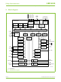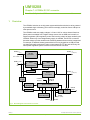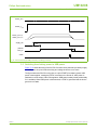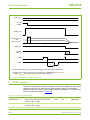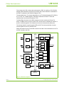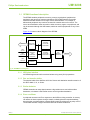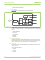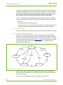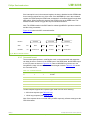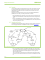
1
UM10208
LPC288x User manual
Rev. 01 — 5 September 2006
User manual
Document information
Info
Content
Keywords
LPC2880, LPC2888, LPC288x, ARM, ARM7, embedded, 32-bit,
microcontroller, USB 2.0, USB HS
Abstract
Initial LPC288x User manual revision
UM10208
Philips Semiconductors
LPC288x User manual
Revision history
Rev
Date
Description
01
20060905
LPC288x User manual
Contact information
For additional information, please visit: http://www.semiconductors.philips.com
For sales office addresses, please send an email to: [email protected]
UM10208_1
User manual
© Koninklijke Philips Electronics N.V. 2006. All rights reserved.
Rev. 01 — 5 September 2006
2 of 338
UM10208
Chapter 1: LPC288x Introductory information
Rev. 01 — 5 September 2006
User manual
1. Introduction
The LPC288x is an ARM7-based microcontroller for portable applications requiring low
power and high performance. It includes a USB 2.0 High Speed device interface, an
external memory interface that can interface to SDRAM and Flash, an MMC/SD memory
card interface, A/D and D/A converters, and serial interfaces including UART, I2C, and I2S.
Architectural enhancements like multi-channel DMA, processor cache, simultaneous
operations on multiple internal buses, and flexible clock generation help ensure that the
LPC288x can handle more demanding applications than many competing devices. The
chip can be powered from a single battery, from the USB, or from regulated 1.8 and 3.3V.
2. Features
•
•
•
•
•
ARM7TDMI processor with 8 kB cache
1 MB on-chip Flash Program Memory with 128-bit access for high performance
64 kB SRAM
32 kB ROM
On-chip DC-DC converter can generate all required voltages from a single battery or
from USB power
• Multiple internal buses allow simultaneous GP DMA, USB DMA, and program
execution from on-chip Flash without contention.
• External memory controller supports Flash, SRAM, ROM, and SDRAM.
• Advanced Vectored Interrupt Controller, supporting up to 30 vectored interrupts
• Innovative Event Router allows interrupt, power-up, and clock-start capabilities from
up to 105 sources
• Multi-channel GP DMA controller that can be used with most on-chip peripherals as
well as for memory-to-memory transfers.
• Serial Interfaces:
–
–
–
–
•
•
•
•
•
•
•
•
•
High Speed USB 2.0 Device (480 or 12 Mbits/s) with on-chip PHYsical layer
UART with fractional baud rate generation, flow control, IrDA support, and FIFOs
I2C Interface
I2S (Inter-IC Sound) interface for independent stereo digital audio input and output
Secure Digital (SD) / MultiMediaCard (MMC) memory card interface
10 bit A/D Converter with 5-channel input multiplexing
16 bit stereo A/D and D/A converters with gain control and optional DMA
Advanced clock generation and power control reduce power consumption
Two 32-bit Timers with selectable prescalers
8-bit LCD interface bus
Real Time Clock can be clocked by 32 kHz oscillator or another source
Watchdog Timer with interrupt and/or reset capabilities
180 pin TFBGA package
UM10208_1
User manual
© Koninklijke Philips Electronics N.V. 2006. All rights reserved.
Rev. 01 — 5 September 2006
3 of 338
UM10208
Philips Semiconductors
Chapter 1: LPC288x Introductory information
3. Applications
• Portable, battery powered devices
• USB devices
4. Architectural overview
The LPC288x includes an ARM7TDMI CPU with an 8kB cache, an AMBA Advanced
High-performance Bus (AHB) interfacing to high speed on-chip peripherals and internal
and external memory, and four AMBA Advanced Peripheral Buses (APBs) for connection
to other on-chip peripheral functions. The LPC288x permanently configures the
ARM7TDMI processor for little-endian byte order.
The LPC288x includes a multi-layer AHB and four separate APBs, in order to minimize
interference between the USB controller, other DMA operations, and processor activity.
Bus masters include the ARM7 itself, the USB block, and the general purpose DMA
controller.
Lower speed peripheral functions are connected to the APB buses. Four AHB-to-APB
bridges interface the APB buses to the AHB bus.
5. ARM7TDMI processor
The ARM7TDMI is a general purpose 32 bit microprocessor that offers high performance
and very low power consumption. The ARM architecture is based on Reduced Instruction
Set Computer (RISC) principles, and the instruction set and related decode mechanism
are much simpler than those of microprogrammed Complex Instruction Set Computers.
This simplicity results in a high instruction throughput and impressive real-time interrupt
response from a small and cost-effective processor core.
Pipeline techniques are employed so that all parts of the processing and memory systems
can operate continuously. Typically, while one instruction is being executed, its successor
is being decoded, and a third instruction is being fetched from memory.
The ARM7TDMI processor also employs a unique architectural strategy known as
THUMB, which makes it ideally suited to high-volume applications with memory
restrictions, or applications where code density is an issue.
The key idea behind THUMB is that of a super-reduced instruction set. Essentially, the
ARM7TDMI processor has two instruction sets:
• The standard 32 bit ARM instruction set.
• A 16 bit THUMB instruction set.
The THUMB set’s 16 bit instruction length allows it to approach twice the density of
standard ARM code while retaining most of the ARM’s performance advantage over a
traditional 16 bit processor using 16 bit registers. This is possible because THUMB code
operates on the same 32 bit register set as ARM code.
THUMB code be as little as 65% of the code size of ARM, and 160% of the performance
of an equivalent ARM processor connected to a 16 bit memory system.
UM10208_1
User manual
© Koninklijke Philips Electronics N.V. 2006. All rights reserved.
Rev. 01 — 5 September 2006
4 of 338
UM10208
Philips Semiconductors
Chapter 1: LPC288x Introductory information
The ARM7TDMI processor is described in detail on the ARM website.
6. On-Chip flash memory system
The LPC2888 includes a 1 MB Flash memory system. This memory may be used for both
code and data storage. Programming of the Flash memory may be accomplished in
several ways. It may be programmed In System via the USB port. The application
program may also erase and/or program the Flash while the application is running,
allowing a great degree of flexibility for data storage and field firmware upgrades.
The Flash is 128 bits wide and includes buffering to allow 3 out of 4 sequential read
operations to operate without wait states.
7. On-Chip Static RAM
The LPC288x includes 64 kB of static RAM that may be used for code and/or data
storage.
8. On-Chip ROM
The LPC288x includes 32 kB of Read Only Memory that may be used for code and/or
constant storage. Execution begins in on-chip ROM after a Reset.
Philips provides a standard boot code in this ROM that reads the state of the Mode inputs
and accordingly does one of the following:
1. starts execution in internal Flash,
2. starts execution in external memory,
3. performs a hardware self-test, or
4. downloads code from the USB interface into on-chip RAM and transfers control to the
downloaded code.
UM10208_1
User manual
© Koninklijke Philips Electronics N.V. 2006. All rights reserved.
Rev. 01 — 5 September 2006
5 of 338
UM10208
Philips Semiconductors
Chapter 1: LPC288x Introductory information
JTAG_SEL
JTAG_TDO
JTAG_TDI
JTAG_TCK
JTAG_TMS
JTAG_TRST
9. Block diagram
LPC2880/2888
JTAG DEBUG
INTERFACE
1 MB
FLASH(1)
64 kB
SRAM
BOOT
ROM
ARM7TDMI-S
FLASH
INTERFACE
SRAM
INTERFACE
ROM
INTERFACE
8 kB CACHE
A[20:0],
D[15:0],
etc.
DP, DM, VBUS,
RREF, CONNECT
EXTERNAL
MEMORY
CONTROLLER
HS USB
WITH DMA
VECTORED
INTERRUPT
CONTROLLER
MULTI-LAYER AHB
+1.5 V
or +5 V
3.3 V,
1.8 V
DC-TO-DC
CONVERTER
AHB TO APB
BRIDGE 0
AHB TO APB
BRIDGE 1
AHB TO APB
BRIDGE 2
START,
STOP
WATCHDOG
TIMER
register
interface
AHB TO APB
BRIDGE 3
SD/MMC CARD
INTERFACE
SYSTEM
CONTROL
UART WITH
IrDA
EVENT
ROUTER
XTALI
XTALO
X32I
X32O
LCD
INTERFACE
CLOCK
OSCILLATOR
GENERATION
AND PLLs
UNIT
OSCILLATOR
I2C-BUS
INTERFACE
REAL-TIME
CLOCK
Px.y
GENERAL
PURPOSE I/O
32-BIT
TIMER 0
AIN[4:0]
10-BIT A/D
CONVERTER
32-BIT
TIMER 1
AINL, AINR
AOUTL,
AOUTR
GP DMA
CONTROLLER
MCLK
MD[3:0], MCMD
TXD, RTS
RXD, CTS
LCD bus
SCL, SDA
DUAL ANALOG
INPUT
FIFO
FIFO
I2S-BUS
INPUT
DATI
BCKI, WSI
DUAL ANALOG
OUTPUT
FIFO
FIFO
I2S-BUS
OUTPUT
DATO
BCKO, DCLKO,
WSO
002aac296
(1) LPC2888 only
Fig 1. LPC288x block diagram
UM10208_1
User manual
© Koninklijke Philips Electronics N.V. 2006. All rights reserved.
Rev. 01 — 5 September 2006
6 of 338
UM10208
Chapter 2: LPC288x Memory addressing
Rev. 01 — 5 September 2006
User manual
1. Memory map and peripheral addressing
ARM processors have a single 4 GB address space. The following table shows how this
space is used on the LPC288x. Addresses not shown in this table are not used.
Table 1.
LPC288x memory usage
Address range General use
Address range details and description
0x0000 0000 to
0x0FFF FFFF
0x0020 0000 - 0x0020 7FFF
Internal ROM (32 kB)
0x0040 0000 - 0x0040 FFFF
Internal RAM (64 kB)
(other addresses)
Software can map other internal and external
memory into this area, to improve its effective
access time.
0x1040 0000 - 0x104F FFFF
Flash (1 MB)
Cacheable area
0x1000 0000 to
0x1FFF FFFF
Internal Memory
0x2000 0000 to
0x5FFF FFFF
External Memory 0x2000 0000 - 0x201F FFFF and Static memory bank 0, 2 MB, STCS0
0x4000 0000 - 0x401F FFFF
0x2400 0000 - 0x241F FFFF and Static memory bank 1, 2 MB, STCS1
0x4400 0000 - 0x441F FFFF
0x2800 0000 - 0x281F FFFF and Static memory bank 2, 2 MB, STCS2
0x4800 0000 - 0x481F FFFF
0x3000 0000 - 0x33FF FFFF and Dynamic memory bank 0, 64 MB
0x5000 0000 - 0x53FF FFFF
0x8000 0000 to
0x8FFF FFFF
Peripherals
See Table 2–2
Includes AHB Peripherals and 4 APBs
1.1 Memory map
The LPC2880/2888 memory map incorporates several distinct regions, as shown in
Figure 2–2. When an application is running, the CPU interrupt vectors are remapped to
allow them to reside in on-chip SRAM.
UM10208_1
User manual
© Koninklijke Philips Electronics N.V. 2006. All rights reserved.
Rev. 01 — 5 September 2006
7 of 338
UM10208
Philips Semiconductors
Chapter 2: LPC288x Memory addressing
4.0 GB
0xFFFF FFFF
reserved
0x9000 0000 to 0xFFFF FFFF
0x9000 0000
0x8FFF FFFF
peripherals
includes AHB and 4 APB buses
0x8000 0000 to 0x8FFF FFFF
reserved
0x5400 0000 to 0x7FFF FFFF
dynamic memory bank 0, 64 MB
0x5000 0000 to 0x53FF FFFF
reserved
0x4820 0000 to 0x4FFF FFFF
static memory bank 2, 2 MB
0x4800 0000 to 0x481F FFFF
reserved
0x4420 0000 to 0x47FF FFFF
static memory bank 1, 2 MB
0x4400 0000 to 0x441F FFFF
reserved
0x4020 0000 to 0x43FF FFFF
static memory bank 0, 2 MB
0x4000 0000 to 0x401F FFFF
reserved
0x3400 0000 to 0x3FFF FFFF
dynamic memory bank 0, 64 MB
0x3000 0000 to 0x33FF FFFF
reserved
0x2820 0000 to 0x2FFF FFFF
static memory bank 2, 2 MB
0x2800 0000 to 0x281F FFFF
reserved
0x2420 0000 to 0x27FF FFFF
static memory bank 1, 2 MB
0x2400 0000 to 0x241F FFFF
reserved
0x2020 0000 to 0x23FF FFFF
static memory bank 0, 2 MB
0x2000 0000 to 0x201F FFFF
reserved
0x1050 0000 to 0x1FFF FFFF
internal flash (1 MB)
0x1040 0000 to 0x104F FFFF
reserved
0x1000 0000 to 0x103F FFFF
reserved
0x0050 0000 to 0x0FFF FFFF
internal RAM (64 kB)
0x0040 0000 to 0x0040 FFFF
internal ROM (32 kB)
0x0020 0000 to 0x0020 7FFF
exception vectors
0x0000 0000 to 0x0000 001F
2.0 GB
external memory
(second instance)
1.0 GB
external memory
(first instance)
internal memory
0x8000 0000
0x7FFF FFFF
0x4000 0000
0x3FFF FFFF
0x2000 0000
0x1FFF FFFF
0x1000 0000
0x0FFF FFFF
remapped area
0.0 GB
0x0000 0000
002aac240
Fig 2. Memory map
UM10208_1
User manual
© Koninklijke Philips Electronics N.V. 2006. All rights reserved.
Rev. 01 — 5 September 2006
8 of 338
UM10208
Philips Semiconductors
Chapter 2: LPC288x Memory addressing
2. Peripheral addressing
Peripheral devices on the LPC288x are distributed among the ARM High-speed Bus
(AHB) and four ARM Peripheral Buses (APBs). The following table indicates which bus
each device is connected to. Addresses not shown in this table are not used.
Table 2.
LPC288x Peripheral devices
Address allocation
Bus
Register addresses (inclusive) Peripheral device
0x8000 0000 - 0x8000 1FFF
APB0
0x8000 0000 - 0x8000 1C00
Event Router
0x8000 2000 - 0x8000 23FF
APB0
0x8000 2000 - 0x8002 027C
Real Time Clock (RTC)
0x8000 2400 - 0x8000 27FF
APB0
0x8000 2400 - 0x8000 2430
10 bit Analog to Digital Converter (ADC)
0x8000 2800 - 0x8000 2BFF
APB0
0x8000 2800 - 0x8000 283C
Watchdog Timer (WDT)
0x8000 3000 - 0x8000 3FFF
APB0
0x8000 3000 - 0x8000 31E8
I/O Configuration (IOCONF)
0x8000 4000 - 0x8000 4BFF
APB0
0x8000 4000 - 0x8000 443C
Clock Generation Unit (CGU) Switchbox
0x8000 4C00 - 0x8000 4FFF
APB0
0x8000 4C00 - 0x8000 4CFC
Clock Generation Unit (CGU)
0x8000 5000 - 0x8000 53FF
APB0
0x8000 5000 - 0x8000 507C
System Configuration Registers
0x8000 8000 - 0x8000 8FFF
AHB
0x8000 8000 - 0x8000 8258
External Memory Controller (EMC)
0x8002 0000 - 0x8000 03FF
APB1
0x8002 0000 - 0x8002 0010
Timer 0
0x8002 0400 - 0x8000 07FF
APB1
0x8002 0400 - 0x8002 0410
Timer 1
0x8002 0800 - 0x8002 0BFF
APB1
0x8002 0800 - 0x8002 082C
I2C Controller
0x8004 0000 - 0x8004 1FFF
AHB
0x8004 0000 - 0x8004 10B4
USB Controller
0x8010 0000 - 0x8010 0FFF
APB2
0x8010 0000 - 0x8010 00BC
Secure Digital / Multimedia Card
Interface (SD/MCI)
0x8010 1000 - 0x8010 1FFF
APB2
0x8010 1000 - 0x8010 1034
0x8010 1FD4 - 0x8010 1FEC
UART
0x8010 2000 - 0x8010 2FFF
APB2
0x8010 2000 - 0x8010 201C
0x8010 2FD8 - 0x8010 2FEC
Flash Programming Interface
0x8010 3000 - 0x8010 33FF
APB2
0x8010 3000 - 0x8010 3080
LCD Interface
0x8010 3800 - 0x8010 3FFF
APB2
0x8010 3800 - 0x8010 38FC
0x8010 3A00 - 0x8010 3A7C
0x8010 3C00 - 0x8010 3C10
GPDMA Controllers
0x8010 4000 - 0x8010 40FF
APB2
0x8010 4000 - 0x8010 4058
ARM7 cache control
0x8020 0000 - 0x8020 007F
APB3
0x8020 0000 - 0x8020 0078
Streaming Analog Input 1 (SAI1)
0x8020 0180 - 0x8020 01FF
APB3
0x8020 0180 - 0x8020 01F8
Streaming Analog Input 4 (SAI4)
0x8020 0200 - 0x8020 027F
APB3
0x8020 0200 - 0x8020 027C
Streaming Analog Output 1 (SAO1)
0x8020 0280 - 0x8020 028F
APB3
0x8020 0280 - 0x8020 02FC
Streaming Analog Output 2 (SAO2)
0x8020 0380 - 0x8020 03FF
APB3
0x8020 0380 - 0x8020 03BC
I2S and Streaming Analog Converters
0x8030 0000 - 0x8030 0FFF
AHB
0x8030 0000 - 0x8030 0474
Interrupt Controller
UM10208_1
User manual
© Koninklijke Philips Electronics N.V. 2006. All rights reserved.
Rev. 01 — 5 September 2006
9 of 338
UM10208
Chapter 3: LPC288x System control block
Rev. 01 — 5 September 2006
User manual
1. Description
The System Control function contains various control and status registers that pertain to
general system operation. This includes control of the boot address used for a warm
reset, and a part identification.
2. Register descriptions
2.1 System Control register map
Table 3.
System Control registers
Names
Description
Access POR Reset
value
Address
SYS_BOOTMAP
Selects boot from ROM or RAM
R/W
0
0x8000 5070
SYS_BOOTADDR Selects the boot address
R/W
0x0020 0000 0x8000 5074
SYS_PARTID
RO
0x0102 100A 0x8000 507C
Provides the part identification
2.2 Boot Map register (SYS_BOOTMAP - 0x8000 5070)
The SYS_BOOTMAP register allows selection of boot from internal ROM or internal RAM
when a warm reset occurs. The addresses used are 0x0020 0000 for ROM and 0x0040
0000 for RAM. Power on reset always results in initial execution from the ROM.
Alternatively, other addresses may be specified by writing a value to the
SYS_BOOTADDR register.
Table 4:
Boot Map register (SYS_BOOTMAP - 0x8000 5070)
Bit
Symbol
Description
Reset
value
0
MAP
This bit allows selecting boot from either ROM or RAM when a warm
0
reset occurs. A 0 in this bit indicates warm boot from ROM, a 1 indicate
warm boot from RAM.
31:1
-
Reserved, user software should not write ones to reserved bits. The
value read from a reserved bit is not defined.
-
2.3 Boot Address register (SYS_BOOTADDR - 0x8000 5074)
The SYS_BOOTADDR register allows selection of a specific memory address to be used
for a warm boot. The address may be any multiple of 1K bytes, specified in the upper bits
of the register. Power on reset always results in initial execution from the ROM.
Table 5:
Boot Address register (SYS_BOOTADDR - 0x8000 5074)
Bit
Symbol
Description
Reset
value
9:0
Unused
These bits always contain 0.
0
31:10 BOOTADDR This field allows selecting a specific address for warm boot.
UM10208_1
User manual
0x0020 0000
© Koninklijke Philips Electronics N.V. 2006. All rights reserved.
Rev. 01 — 5 September 2006
10 of 338
UM10208
Philips Semiconductors
Chapter 3: LPC288x System control
2.4 Part Identification register (SYS_PARTID - 0x8000 507C)
The SYS_PARTID register contains a value that identifies this device as either an
LPC2880 or LPC2888 (but not which).
Table 6:
Part Identification register (SYS_PARTID - 0x8000 507C)
Bit
Symbol
Description
Reset
value
31:0
PART_ID
This value distinguishes this device type.
0x0102 100A
UM10208_1
User manual
© Koninklijke Philips Electronics N.V. 2006. All rights reserved.
Rev. 01 — 5 September 2006
11 of 338
UM10208
Chapter 4: LPC288x Boot process
Rev. 01 — 5 September 2006
User manual
1. Introduction
Upon reset, the LPC288x executes code from an internal ROM. This code allows four
possible types of startup. These are:
•
•
•
•
Execute code from internal flash memory.
Execute code from external memory bank 0.
Download code from USB to memory.
Test mode. Toggles a port pin to indicate basic device functionality.
2. Operation
Internal pulldowns on the P2.3 and P2.2 pins cause them to read as 0 when unconnected.
This results in the default startup mode being execution from internal Flash memory. One
or two external pullup resistors can cause startup to use one of the other modes, as
shown in Table 4–7.
Table 7.
Boot flow chart
P2.3/Mode2
P2.2/Mode1 Mode selected
0
0
Execute user program from internal flash memory.
0
1
Execute user program from external memory on bank 0.
1
0
Download program from USB port to memory.
1
1
Test mode.
3. Boot mode descriptions
The boot process is illustrated in figure 1. The following discussion describes each boot
mode in more detail.
Mode 0: Execute user program from internal flash memory
This is the default mode if the P2.3 and P2.2 pins are left unconnected. The Flash
memory begins at address 0x1040_0000. This is the address branched to in this mode.
In order to prevent accidental execution of an unprogrammed Flash, the ROM code
checks for a specific valid user program marker value in memory prior to branching into
the Flash memory. This marker is stored as address 0x104F_F800, 2K bytes below the
top of the 1MB Flash memory. The value expected here is 0xAA55_AA55. If Mode 0 is
selected and the valid user program marker value is not found in the Flash, control is
transferred to Mode 2 (USB download mode).
UM10208_1
User manual
© Koninklijke Philips Electronics N.V. 2006. All rights reserved.
Rev. 01 — 5 September 2006
12 of 338
UM10208
Philips Semiconductors
Chapter 4: LPC288x Boot process
Mode 1: Execute user program from external memory on static memory bank 0
Static bank 0 of external memory controller is used in a default configuration to execute a
user program. The configuration of static bank 0 following reset is for a bus width of 16 bits
and an active low chip select. The starting address used for the external static memory is
0x2000_0000. The full address range for bank 0 is 0x4000_0000 through 0x401F_FFFF,
a 2 megabyte space.
Mode 2: Download program from USB port to memory (DFU mode)
The purpose of this mode is to allow programming of the internal Flash memory via USB.
Files to be download must be specially formatted in order to be handled by the ROM
download code. A conversion program and a DFU downloader are available from Philips.
Mode 3: Test mode
This mode is a simple test for device function. Port pin P2.1 is toggled to indicate basic
functionality of the device in its current environment.
UM10208_1
User manual
© Koninklijke Philips Electronics N.V. 2006. All rights reserved.
Rev. 01 — 5 September 2006
13 of 338
UM10208
Philips Semiconductors
Chapter 4: LPC288x Boot process
Reset
Basic Initialization
- disable interrupts
- disable cache
- initialize CGU
Mode = 3?
Y
- Continuously toggle pin P2.1
N
Initialize exception modes
Initialize external memory
controller
Initialize internal memory
systems
Mode = 1?
Y
- Branch to first bank 0 address.
N
Mode = 2?
Y
- USB download
N
Flash ready?
N
Y
Valid User
Program
Marker?
N
Y
- Branch to first Flash address.
Fig 3. Boot process
UM10208_1
User manual
© Koninklijke Philips Electronics N.V. 2006. All rights reserved.
Rev. 01 — 5 September 2006
14 of 338
UM10208
Chapter 5: LPC288x Processor cache and memory mapping
Rev. 01 — 5 September 2006
User manual
1. Introduction
The ARM CPU in the LPC288x has been extended with a 2-way set-associative cache
controller. The cache is 8 kB in size and can store both data and instruction code.
The biggest benefit of this cache is that if code is run from non-zero-wait state memory, for
instance the internal FLASH controller, these memories can still behave almost as if they
are zero-wait state memory. If code is executed from the cache, the CPU will run at 1
clock per instruction most of the time.
The trade-off in introducing this cache is that each AHB access that bypasses the cache
will have an extra wait state inserted. So, it is generally advisable that both instruction
caching and data caching are turned on for most regions of on and off-chip memory.
2. Features
• 8 kB in a 2-way set-associative cache
• Configured as 2×128 cache lines of eight 32-bit words each
• Sixteen pages of address mapping each allow any address range to be selected for
caching
3. Cache definitions
• A 2-way cache includes two cache lines that can be used for each memory address.
• A cache line is 8 consecutive 32 bit words. The cache contains 128 cache lines, each
with 2 ways, making 8 kB total.
• The association of memory addresses to cache lines is that cache line 0 corresponds
with address word addresses 0x0 to 0x07, cache line 1 corresponds with word
addresses 0x08 to 0x0F, etc. After 1024 words, this repeats. Thus, word address 0,
word address 1024, word address 2048, ... all map to cache line 0.
• A tag word is associated with each cache line. The tag includes the address each
cache line is currently associated with, a "dirty" flag that indicates if the line has been
written to since it was read from memory, and a "Least Recently Used" tag that
identifies which of the two cache lines should be overwritten if another address that
maps there is accessed by the CPU.
• For the purposes of cache operation, memory is divided into pages of 2 megabytes,
composed of 4 kB sub-pages (1024 words of 32 bits).
• A cache line is marked as "dirty" when the CPU writes to an address which is
currently in the cache. In this case, the data in the "real" memory no longer reflects the
actual value. The entire cache line is marked as dirty when any element within that
cache line is written.
• A cache miss is defined as a read or write by the CPU to an address in memory which
is not currently in the cache.
UM10208_1
User manual
© Koninklijke Philips Electronics N.V. 2006. All rights reserved.
Rev. 01 — 5 September 2006
15 of 338
UM10208
Philips Semiconductors
Chapter 5: LPC288x Processor cache
• A cache hit is defined as a read or write by the CPU to an address in memory which is
currently in cache.
• A cache flush is the act of writing a dirty cache line back to memory.
4. Description
Figure 5–4 shows the structure of the cache and how memory addresses map to cache
lines. For caching purposes, memory is divided into pages of 2 megabytes of 4 kB
sub-pages (1024 words of 32 bits). The sub-pages correspond to 128 cache lines (128
entries of eight 32-bit words).
The associated cache line in memory will be stored in cache memory at a fixed position.
An example sequence could begin with an access to one of the first 8 words of a 2
megabyte page of memory. These words will be stored on the first cache line (cache line
0) of Way_0. An access to one of the second 8 words in the same page will be stored on
the second cache line (cache line 1) of Way_0. Later, if an address that maps to cache
line 0 is read from a different portion of memory, it will be stored in Way_1 (since Way_1
has not yet been used). If still another address mapping to cache line 0 is read, the Least
Recently Used tag is used to decide whether the new line will be stored in Way_0 or
Way_1. The least recently used previously cached line must be removed, and the new
line stored in its place. In this example, the way that is overwritten will be Way_0, since
Way_1 was used more recently. If the cache line that must be removed is marked as
“dirty”, it will be written back to memory prior to being overwritten by the new memory line.
Note that the cache can be set to work only for instruction accesses, only for data
accesses, or for both. This is done via the DATA_ENABLE and INSTRUCTION_ENABLE
bits in the CACHE_SETTINGS register.
UM10208_1
User manual
© Koninklijke Philips Electronics N.V. 2006. All rights reserved.
Rev. 01 — 5 September 2006
16 of 338
UM10208
Philips Semiconductors
Chapter 5: LPC288x Processor cache
Memory
Word 0
Word 1
Way_0
4K bytes
line 0
line 1
Way_1
4K bytes
line 0
line 1
line 128
line 128
Read into
cache line 0
Word 7
Word 8
128 * 8
Words
Read into
cache line 1
Word 15
2M
bytes
Second read
into cache line 0
128 * 8
Words
Third read into
cache line 0
128 * 8
Words
Fig 4. Cache operation
The cache has 16 configurable pages, each being 2 megabytes in size. The cache treats
these 16 pages as if they occupy the bottom 32 Megabytes of the system memory map,
which is their default mapping. The cache can re-map any of these pages such that the
physical address is above the lower 32 megabytes.
In Figure 5–5, a diagram showing physical memory and a virtual page mapping is given.
On the left of the diagram, memory is shown with no remapping, as issued by the CPU.
On the right, a higher physical address is shown mapped into a lower address for caching
purposes. To accomplish this, a page is used as a virtual page. Accessing this virtual
page, the cache will re-map the AHB bus address to the higher address range during a
cache miss, cache flush or a write access to the virtual page.
UM10208_1
User manual
© Koninklijke Philips Electronics N.V. 2006. All rights reserved.
Rev. 01 — 5 September 2006
17 of 338
UM10208
Philips Semiconductors
Chapter 5: LPC288x Processor cache
In Figure 5–5, page 2 of the lower 32 megabytes of address space has been mapped to
an address in the external static memory space by placing a value of 0x104 in the
PAGE_ADDRESS_2 register. Details of this remapping may be found in the descriptions
of the PAGE_ADDRESS registers later in this chapter.
When re-mapping points to a higher page in the memory map, that page may still also be
accessed directly by the CPU using the original absolute address of the page. In that
case, the cache takes no part in the access. This allows both cached and non-cached
access to the same address region if needed.
Each of the 16 configurable cache pages can be individually enabled and disabled, as
well as having a virtual address programmed.
Memory
(address as seen
by the AHB bus)
Memory
(address as issued
by the CPU)
0x0000_0000
0x0000_0000
Page 0
0x0020_0000
Page 1
0x0040_0000
First
32 M
bytes
Page 2
First
32 M
bytes
0x0040_0000
Address remapped
by value in
ADDRESS_PAGE_2
Page 16
0x0200_0000
0x0200_0000
Above
32 M
bytes
External
SRAM
0x2080_0000
0x2080_0000
External
SRAM
Above
32 M
bytes
Fig 5. Memory mapping
UM10208_1
User manual
© Koninklijke Philips Electronics N.V. 2006. All rights reserved.
Rev. 01 — 5 September 2006
18 of 338
UM10208
Philips Semiconductors
Chapter 5: LPC288x Processor cache
4.1 Cache enabling and function
Following reset, the cache is disabled. The address, data, and control signals of the CPU
AHB bus is routed directly to the multilayer AHB matrix. The response from whichever
functional block is targeted by the address is routed directly to the CPU.
The cache can be enabled by setting the DATA_ENABLE and/or
INSTRUCTION_ENABLE bits in the CACHE_SETTINGS register.
4.1.1 Cache function details
For each page of the cache which is enabled, the following points apply:
• If data is read, and not in the cache (a cache miss), a line of eight 32-bit words is read
from the AHB bus. In the meantime, the CPU is stalled (and in low power mode if
clock gating is enabled.)
• If data is read and is found in the cache (a cache hit), data is read from cache with 0
wait states.
• If data is written and the location is not in the cache (a cache miss), the data is written
directly to memory.
• If data is written, and the location is in the cache because this location has been read
before (a cache hit), then data is written to the cache with 0 wait states, and the line is
marked as dirty.
• If a dirty line is about to be discarded because of a cache miss (the cache line needs
to be reused for a different memory region), the old line is first written back to memory
(a cache line flush).
• When a cache line is read from memory and stored in the cache (in Way_0 or
Way_1), the cache controller will mark the other half of the cache line at the same
address as Least Recently Used (LRU) in its tag memory.
5. Register description
The cache controller includes the registers shown in Table 5–8. These registers are
accessible in the APB2 address space. It is recommended that the clock gating option be
enabled in the CGU for the APB interface of the CPU in order to reduce power
consumption. Each register is described in more detail in the following sections.
Note: the APB interface of the CPU configuration hardware must be set to run at the same
BASE_CLK frequency as the AHB interface of the CPU before any register is written.
Table 8.
Cache and memory mapping registers
Address
Register name
Description
Reset
value
Access
0x8010 4000
CACHE_RST_STAT
Monitors the reset state of the cache.
0
RO
0x8010 4004
CACHE_SETTINGS
Controls the overall configuration of the cache.
0
R/W
0x8010 4008
CACHE_PAGE_CTRL
Allows individual enabling or disabling of caching for the
16 configurable pages.
0
R/W
0x8010 400C
C_RD_MISSES
If cache performance analysis is enabled in the
CACHE_SETTINGS register, this register indicates the
number of times that a cache line is read from memory
(cache read misses).
0
RO
UM10208_1
User manual
© Koninklijke Philips Electronics N.V. 2006. All rights reserved.
Rev. 01 — 5 September 2006
19 of 338
UM10208
Philips Semiconductors
Chapter 5: LPC288x Processor cache
Table 8.
Cache and memory mapping registers
Address
Register name
Description
Reset
value
Access
0x8010 4010
C_FLUSHES
If cache performance analysis is enabled in the
CACHE_SETTINGS register, this register indicates the
number of times that a dirty cache line has been written
back to memory (cache flushes).
0
RO
0x8010 4014
C_WR_MISSES
If cache performance analysis is enabled in the
CACHE_SETTINGS register, this register indicates the
number of times that a write occurs to an address not in
the cache (cache write misses).
0
RO
0x8010 4018
PAGE_ADDRESS_0
Re-mapping address for page 0.
0
R/W
0x8010 401C
PAGE_ADDRESS_1
Re-mapping address for page 1. The reset value points
this page to the Boot ROM.
0x1
R/W
0x8010 4020
PAGE_ADDRESS_2
Re-mapping address for page 2. The reset value points
this page to the on-chip SRAM.
0x2
R/W
0x8010 4024
PAGE_ADDRESS_3
Re-mapping address for page 3. The reset value points
this page to the on-chip SRAM.
0x2
R/W
0x8010 4028
PAGE_ADDRESS_4
Re-mapping address for page 4. The reset value points
this page to on-chip Flash memory.
0x82
R/W
0x8010 402C
PAGE_ADDRESS_5
Re-mapping address for page 5. The reset value points
this page to external static memory bank 0.
0x100
R/W
0x8010 4030
PAGE_ADDRESS_6
Re-mapping address for page 6. The reset value points
this page to external static memory bank 0.
0x100
R/W
0x8010 4034
PAGE_ADDRESS_7
Re-mapping address for page 7. The reset value points
this page to external SDRAM.
0x180
R/W
0x8010 4038
PAGE_ADDRESS_8
Re-mapping address for page 8. The reset value points
this page to external SDRAM.
0x180
R/W
0x8010 403C
PAGE_ADDRESS_9
Re-mapping address for page 9.
0x400
R/W
0x8010 4040
PAGE_ADDRESS_10
Re-mapping address for page 10.
0x401
R/W
0x8010 4044
PAGE_ADDRESS_11
Re-mapping address for page 11.
0x102
R/W
0x8010 4048
PAGE_ADDRESS_12
Re-mapping address for page 12.
0x104
R/W
0x8010 404C
PAGE_ADDRESS_13
Re-mapping address for page 13.
0x106
R/W
0x8010 4050
PAGE_ADDRESS_14
Re-mapping address for page 14.
0xE
R/W
0x8010 4054
PAGE_ADDRESS_15
Re-mapping address for page 15.
0xF
R/W
0x8010 4058
CPU_CLK_GATE
Controls gating of the CPU clock when the CPU is
stalled.
0
R/W
5.1 Cache Reset Status register (CACHE_RST_STAT, 0x8010 4000)
The read-only CACHE_RST_STAT register monitors the reset status of the cache
controller. If the CACHE_RST bit in the CACHE_SETTINGS register is set and then
cleared by software, this bit indicates the status of the ongoing reset. The reset of the
cache tag memory will take 128 CPU clock-cycles to complete. Table 5–9 shows the bit
definitions for the CACHE_RST_STAT register.
UM10208_1
User manual
© Koninklijke Philips Electronics N.V. 2006. All rights reserved.
Rev. 01 — 5 September 2006
20 of 338
UM10208
Philips Semiconductors
Chapter 5: LPC288x Processor cache
Table 9.
Cache Reset Status register (CACHE_RST_STAT, 0x8010 4000)
Bit
Symbol
Description
0
CACHE_STATUS 0: Cache reset is complete.
Reset
value
0
1: Cache reset is ongoing.
When the cache is reset, software should poll
CACHE_STATUS until it is 0.
31:1
-
Reserved. The value read from a reserved bit is not defined.
-
5.2 Cache Settings register (CACHE_SETTINGS, 0x8010 4004)
The CACHE_SETTINGS register controls the general setup of the cache, allows resetting
of the entire cache, and controls the cache performance analysis feature. Table 5–10
shows the bit definitions for the CACHE_SETTINGS register.
Table 10.
Cache Settings register (CACHE_SETTINGS, 0x8010 4004)
Bit
Symbol
Description
Reset
value
0
CACHE_RST
Cache controller reset control. This bit resets the cache 0
hardware internally, clearing all tags so that the entire
cache is considered empty. This takes 128 CPU clock
cycles to complete. The reset progress can be followed
by reading register CACHE_RST_STAT.
0 : De-assert reset to the Flash controller.
1 : Assert reset to the Flash controller.
Note: the cache MUST be reset before it is enabled. It is
recommended to include this procedure at system
startup.
1
DATA_ENABLE
Enables use of the cache for storing data.
0
0 : All storage of data in the cache is disabled. This
applies to all 16 pages.
1 : Storage of data in the cache is enabled. This applies
to all pages enabled via the CACHE_PAGE_CTRL
register.
2
INSTRUCTION_ENABLE Enables use of the cache for storing instructions.
0
0 : All storage of instructions in the cache is disabled.
This applies to all 16 pages.
1 : Storage of instructions in the cache is enabled. This
applies to all pages enabled via the
CACHE_PAGE_CTRL register.
UM10208_1
User manual
© Koninklijke Philips Electronics N.V. 2006. All rights reserved.
Rev. 01 — 5 September 2006
21 of 338
UM10208
Philips Semiconductors
Chapter 5: LPC288x Processor cache
Table 10.
Cache Settings register (CACHE_SETTINGS, 0x8010 4004)
Bit
Symbol
Description
Reset
value
3
PERF_ANAL_RST
Allows a software reset of the cache performance
analysis counters in the registers C_RD_MISSES,
C_FLUSHES, and C_WR_MISSES.
0
0 : Allow performance analysis counters to run, if
enabled.
1 : Reset the cache performance analysis counters.
This has an effect only if performance analysis is
enabled.
4
PERF_ANAL_ENA
Controls the cache performance analysis counters in
the registers C_RD_MISSES, C_FLUSHES, and
C_WR_MISSES. Performance analysis should be
disabled when not needed in order to save power.
0
0 : Performance analysis is disabled.
1 : Performance analysis is enabled.
31:5 -
Reserved. Do not write 1s to reserved bits. The values
read from reserved bits is not defined.
-
5.3 Cache Page Enable Control register (CACHE_PAGE_CTRL,
0x8010 4008)
The CACHE_PAGE_CTRL register allows individual enabling of caching of each of the 16
pages. Table 5–11 shows the bit definitions for the CACHE_PAGE_CTRL register.
Table 11.
Cache Page Enable Control register (CACHE_PAGE_CTRL, 0x8010 4008)
Bit
Symbol
Description
Reset
value
0
PAGE_0_ENA
This bit enables caching for page 0.
0
0: Caching for this page is disabled.
1: Caching for this page is enabled.
1
PAGE_1_ENA
This bit enables caching for page 1, as described for bit 0.
0
2
PAGE_2_ENA
This bit enables caching for page 2, as described for bit 0.
0
3
PAGE_3_ENA
This bit enables caching for page 3, as described for bit 0.
0
4
PAGE_4_ENA
This bit enables caching for page 4, as described for bit 0.
0
5
PAGE_5_ENA
This bit enables caching for page 5, as described for bit 0.
0
6
PAGE_6_ENA
This bit enables caching for page 6, as described for bit 0.
0
7
PAGE_7_ENA
This bit enables caching for page 7, as described for bit 0.
0
8
PAGE_8_ENA
This bit enables caching for page 8, as described for bit 0.
0
9
PAGE_9_ENA
This bit enables caching for page 9, as described for bit 0.
0
10
PAGE_10_ENA This bit enables caching for page 10, as described for bit 0.
0
11
PAGE_11_ENA This bit enables caching for page 11, as described for bit 0.
0
12
PAGE_12_ENA This bit enables caching for page 12, as described for bit 0.
0
13
PAGE_13_ENA This bit enables caching for page 13, as described for bit 0.
0
UM10208_1
User manual
© Koninklijke Philips Electronics N.V. 2006. All rights reserved.
Rev. 01 — 5 September 2006
22 of 338
UM10208
Philips Semiconductors
Chapter 5: LPC288x Processor cache
Table 11.
Cache Page Enable Control register (CACHE_PAGE_CTRL, 0x8010 4008)
Bit
Symbol
14
PAGE_14_ENA This bit enables caching for page 14, as described for bit 0.
0
15
PAGE_15_ENA This bit enables caching for page 15, as described for bit 0.
0
31:16 -
Description
Reset
value
Reserved. Do not write 1s to reserved bits. The values read
from reserved bits is not defined.
-
Note: If data caching has been enabled for a writable page, and software then disables
caching, there may be “dirty data” in the cache that still needs to be written to memory.
5.4 Cache Read Misses counter (C_RD_MISSES, 0x8010 400C)
The C_RD_MISSES register allows reading the number of times that a cache line fill has
occurred (a cache read miss) since the last time that the performance analysis registers
have been reset. The counter only operates if performance analysis has been enabled via
the PERF_ANAL_ENA bit in the CACHE_SETTINGS register. In order to save power,
performance analysis should be turned off if it is not actually being used.
5.5 Cache Flushes counter (C_FLUSHES, 0x8010 4010)
The C_FLUSHES register allows reading the number of times that a cache line has been
written back to memory (a cache flush) since the last time that the performance analysis
registers have been reset. A cache line is written back to memory only if it has been
marked as dirty (due to its contents being changed) and the cache line is subsequently
required for normal continuing cache operation. The counter only operates if performance
analysis has been enabled via the PERF_ANAL_ENA bit in the CACHE_SETTINGS
register. In order to save power, performance analysis should be turned off if it is not
actually being used.
5.6 Cache Write Misses counter (C_WR_MISSES, 0x8010 4014)
The C_WR_MISSES register allows reading the number of times that a write has
occurred to a memory address that is not in the cache (a cache write miss). The counter
only operates if performance analysis has been enabled via the PERF_ANAL_ENA bit in
the CACHE_SETTINGS register. In order to save power, performance analysis should be
turned off if it is not actually being used.
5.7 Page Address Pointer Registers (PAGE_ADDRESS0:15,
0x8010 4018:4054)
The 16 PAGE_ADDRESS registers allow remapping of addresses in the range supported
by the cache (the bottom 32 megabytes of memory space) so that they apply to other
address ranges. When the CPU performs an access to an address in the cache range,
any value in the related PAGE_ADDRESS register will replace the top 11 bits of the 32-bit
address. By leaving the bottom 21 bits unaltered, each increment of the value in an
PAGE_ADDRESS register corresponds to a shift of 2 megabytes. In this manner, software
can control which memory address ranges are cached.
For example, if the CPU accesses the address 0x0121_4A90, and the
PAGE_ADDRESS_9 register contains the value 0x82, caching activity and the CPU
access will apply to address 0x1041_4A90:
UM10208_1
User manual
© Koninklijke Philips Electronics N.V. 2006. All rights reserved.
Rev. 01 — 5 September 2006
23 of 338
UM10208
Philips Semiconductors
Chapter 5: LPC288x Processor cache
Original address: 0121_4A90 =
Top 11 address bits removed:
Address bits from PAGE_ADDRESS9 ( 082) =
Top 11 address bits replaced: 1041_4A90 =
0000
0000
0001
0001
0001
0000
0000
0000
0010 0001 _ 0100 1010 1001 0000
0000 0001 _ 0100 1010 1001 0000
010
0100 0001 _ 0100 1010 1001 0000
This particular setting maps page 9 of the cacheable address space to the on-chip Flash
memory starting at address 0x1040_0000.
Table 5–12 shows the address ranges covered by each of the PAGE_ADDRESS
registers, and Table 5–13 shows the use of bits in each register.
Table 12.
Address ranges used by PAGE_ADDRESS registers
Register
2 megabyte
multiple
Bottom of related
address range
Top of related
address range
PAGE_ADDRESS_0
0
0x0000 0000
0x001F FFFF
PAGE_ADDRESS_1
1
0x0020 0000
0x003F FFFF
PAGE_ADDRESS_2
2
0x0040 0000
0x005F FFFF
PAGE_ADDRESS_3
3
0x0060 0000
0x007F FFFF
PAGE_ADDRESS_4
4
0x0080 0000
0x009F FFFF
PAGE_ADDRESS_5
5
0x00A0 0000
0x00BF FFFF
PAGE_ADDRESS_6
6
0x00C0 0000
0x00DF FFFF
PAGE_ADDRESS_7
7
0x00E0 0000
0x00FF FFFF
PAGE_ADDRESS_8
8
0x0100 0000
0x011F FFFF
PAGE_ADDRESS_9
9
0x0120 0000
0x013F FFFF
PAGE_ADDRESS_10 10
0x0140 0000
0x015F FFFF
PAGE_ADDRESS_11
11
0x0160 0000
0x017F FFFF
PAGE_ADDRESS_12 12
0x0180 0000
0x019F FFFF
PAGE_ADDRESS_13 13
0x01A0 0000
0x01BF FFFF
PAGE_ADDRESS_14 14
0x01C0 0000
0x01DF FFFF
PAGE_ADDRESS_15 15
0x01E0 0000
0x01FF FFFF
Table 13.
Page Address Pointer Registers (PAGE_ADDRESS0:15, 0x8010 4018:4054)
Bit
Symbol
Description
Reset
value
10:0
UPPR_ADDR
This value will replace the top 11 bits of the 32-bit
see
address coming from the CPU. When the CPU performs Table 5–8
an access to the related page, the address which is
placed on the AHB bus will depend on the value of this
register.
31:11
-
Reserved. Do not write 1s to reserved bits. The values
read from reserved bits is not defined.
-
5.8 CPU Clock Gate control (CPU_CLK_GATE, 0x8010 4058)
The CPU_CLK_GATE register allows saving power by gating the CPU clock when the
CPU is stalled waiting for bus access. Table 5–14 shows the bit definitions for the
CPU_CLK_GATE register.
UM10208_1
User manual
© Koninklijke Philips Electronics N.V. 2006. All rights reserved.
Rev. 01 — 5 September 2006
24 of 338
UM10208
Philips Semiconductors
Chapter 5: LPC288x Processor cache
Table 14.
CPU Clock Gate control (CPU_CLK_GATE, 0x8010 4058)
Bit
Symbol
Description
Reset
value
0
CPU_CLK_GATE This bit controls clock gating to the CPU. When clock gating is 0
enabled, power is saved by not clocking the CPU when it is
stalled waiting for bus access.
0: The CPU clock is running continuously.
1: The CPU clock is gated off while the CPU is stalled.
31:1
-
Reserved. Do not write 1s to reserved bits. The values read
from reserved bits is not defined.
-
6. Cache programming procedures
6.1 Cache initialization
1. Clear the cache:
Set and reset the CACHE_RST bit in the CACHE_SETTINGS register (one clock
cycle is sufficient).
The status flag CACHE_RST_STAT in the CACHE_STATUS indicates whether a
cache reset is ongoing. Software should poll this bit before the cache is enabled.
2. Program the virtual address for each page, if needed:
Software can enable those parts of the memory map that are to be cacheable, by
setting the appropriate bits in the CACHE_PAGE_CTRL register.
Each bit represents one page (2 megabytes) of memory space:
– bit 0 enables 0x0000_0000 to 0x0020_0000 as cached (page 0),
– bit 1 enables 0x0020_0000 to 0x0040_0000 as cached (page 1),
– bit 2 enables 0x0040_0000 to 0x0060_0000 as cached (page 2),
– etc.
3. Program the virtual address for each page, if needed:
The 11 bits programmed for each page represents the top 11 bits of a 32-bit address
that will be put on the AHB bus. This allows any part of the entire 32-bit address range
to be remapped into the bottom 32 megabytes of space, in pages of 2 megabytes.
The PAGE_ADDRESS registers DO NOT reset to a value such that remapping is not
in force, so they should always be initialized even if remapping is not needed in the
application.
Example:
Say address location 0x10400000 (in on-chip Flash) must be mapped for page 3.
That can be done this way:
*PAGE_ADDRESS_3 = (0x10400000 >> 21); // = 0x082;
If the CPU reads address 0x00600004 (an address inside page 3) , then address
0x10400004 is provided to the AHB bus.
Note: care must be taken if remapping a page from which the code is currently
running, or a page that is being used for data, stack or heap storage.
4. Enable the cache for data and /or instructions:
UM10208_1
User manual
© Koninklijke Philips Electronics N.V. 2006. All rights reserved.
Rev. 01 — 5 September 2006
25 of 338
UM10208
Philips Semiconductors
Chapter 5: LPC288x Processor cache
Enable the cache by setting the DATA_ENABLE and/or INSTRUCTION_ENABLE bits
in the CACHE_SETTINGS register.
For enabling cache functions, these two bits apply to all cache pages that are enabled
via the CACHE_PAGE_CTRL register. For disabling cache functions, these bits apply
to all 16 cache pages, regardless of the setting of the CACHE_PAGE_CTRL register.
The entire cache can be programmed to:
– cache only instructions
– cache only data
– cache both instructions and data
If neither of the two enable bits is set, the cache is disabled.
6.2 Cache flushing
Cache flushing may be required if caching of data is enabled, or when the virtual address
of a page must be changed while this page has caching enabled. Cache flushing is only
necessary if data-caching is enabled.
If data is written to cached memory, the new data will initially end up only inside the cache,
and the related cache line marked as dirty. This data is not yet stored in the true physical
location in memory. Since the cache applies only to the ARM7, not to other AHB masters,
if another master (such as the GPDMA) is programmed to copy this data, it will copy the
old data. If the programmer wants to guarantee that the data inside the cache is written to
memory, the programmer has to flush the cache.
The cache controller does not include a direct method to cause an immediate cache flush.
If software needs to flush the entire cache, a simple way to accomplish this is to fill the
cache with read-only data (for instance ROM data). This results in every cache line being
checked to see if it is dirty, and written back to memory if needed. Only 1 out of the 8
words from memory corresponding to each cache line must be read in order to flush one
cache line. A total of 256 cache lines must be read in order to fully flush the cache. Below
is a C language example to replace the cache contents, thereby flushing its the cache.
void flush_cache (int * cache_start) {
volatile int * flush_pointer = (volatile int *) cache_start;
volatile int cache_dummy;
int i;
for (i=0;i<2048;i+=8) cache_dummy = flush_pointer[i];
}
Example: Calling the flush_cache procedure with a value of 0x1200 will read 8 kB of
read-only code starting from 0x1200 into the cache, effectively flushing all dirty data from
the cache.
A subset of this procedure could be used to flush a portion of the cache (as little as one
cache line) if the line and its original address is known. Any two data locations other than
the location of the currently cached data that maps to the same cache line can be read.
This will cause any of the originally cached data to be flushed if it is marked as dirty.
Cache flushing may be necessary in the following cases:
UM10208_1
User manual
© Koninklijke Philips Electronics N.V. 2006. All rights reserved.
Rev. 01 — 5 September 2006
26 of 338
UM10208
Philips Semiconductors
Chapter 5: LPC288x Processor cache
1. When data caching is enabled for a page, and another bus master such as the GPMA
uses this data as well.
2. When data caching is enabled for a page, and caching for this page is about to be
disabled. When the caching for a page is disabled, every word is read directly from
memory, bypassing the cache. If any data has been written to that page, the CPU may
read the wrong data.
3. When data caching in the CACHE_SETTINGS register is about to be disabled. This is
a more general version of case 2.
4. When the virtual address of a cached page is about to be changed. This applies for
both instruction and data caching. The cache controller is not aware of any changes
made to the address mapping. If the address mapping is changed, software must
ensure that any altered cache contents are flushed. Also, if code was executed from
the page that is about to be remapped, it must be flushed to prevent later execution of
the wrong instructions.
6.3 Avoiding cache flushing
It may be possible to avoid cache flushing in some cases. If the performance difference is
not critical, data caching can simply not be enabled. Performance reductions in the 20 to
30% range are possible if data caching is disabled, depending on the application.
Another way to avoid data caching in certain cases is to have 2 pages that point to the
same memory address range. One page would be set as cacheable, the other as not
cacheable. Data written to the non-cached page is written directly to memory, so other bus
masters can make use of this data without any need to flush the cache. Care must be
taken not to write data to one page, and read the same data from the other page. This can
be done by separating portions of the page that may be changing from portions that will
not be changing. Changeable portions would be both read and written in the non-cached
address range, while static data would be read from the cached address range.
6.4 CPU and cache clocking
The CPU clocking is somewhat different than the rest of the AHB system. Where the rest
of the AHB system is clocked by the CGU (the AHB-BASE_CLOCK, possibly modified by
a fractional divider), the CPU and cache system use the AHB clock as a reference to
generate internal clocks from the AHB_BASE_CLOCK. Inside the cache system is a
clock-gate that uses the reference clock to enable or disable the base clock going to the
CPU and cache system.
Figure 5–6 shows timing of some cases of different clock selection settings. These figures
show some internal signals to illustrate the timing. First, “CPU clock” is the clock as seen
by the CPU. Second, “CPU clock enable” is the signal that determines when the CPU
receives a clock when clock gating is enabled. The CPU clock enable signal goes low one
AHB clock prior to the time when the CPU clock is prevented.
Following is a description of each case shown:
1. CPU clock gating off, fractional divider not used.
In this case, there is no CPU clock-gating and a fractional divider for the AHB clock is
not selected. This results in a free-running clock for the AHB, cache and CPU, all
running at the same frequency. This is the reset condition of the system.
UM10208_1
User manual
© Koninklijke Philips Electronics N.V. 2006. All rights reserved.
Rev. 01 — 5 September 2006
27 of 338
UM10208
Philips Semiconductors
Chapter 5: LPC288x Processor cache
2. CPU clock gating off, fractional divider set to 1/7.
In this case, the AHB fractional divider has been set to generate a bus clock once
every 7 base clock cycles.
3. CPU clock gating enabled, fractional divider set to 1/7.
In this case, CPU clock gating has been enabled. The CPU clock enable signal is
generated by the cache when the CPU must wait because either the cache is reading
or writing data on the AHB bus, or the cache is jumping in between cache lines,
adding a single wait state.
CPU clock
AHB0 clock
Internal cache clock
Internal CPU clock
CPU clock enable
Case 1: CPU clock gating off, fractional divider not used.
CPU clock
AHB0 Clock
Internal cache clock
Internal CPU clock
CPU clock enable
Case 2: CPU clock gating off, fractional divider set to 1/7.
CPU clock
AHB0 Clock
Internal cache clock
Internal CPU clock
CPU clock enable
Case 3: CPU clock gating enabled, fractional divider set to 1/7.
Fig 6. Cache and CPU clock timing
UM10208_1
User manual
© Koninklijke Philips Electronics N.V. 2006. All rights reserved.
Rev. 01 — 5 September 2006
28 of 338
UM10208
Chapter 6: LPC288x Flash interface and programming
Rev. 01 — 5 September 2006
User manual
1. Introduction
The LPC2888 includes one megabyte of flash memory. This memory is located on the
AHB and is accessible by all AHB masters. In contrast, the LPC2880 does not include any
on-chip flash memory.
2. Features
• Flash memory is an AHB slave for data transfer.
• APB slave interface for programmatic flash programming and erasure.
• Interrupt capability when flash erasure or programming is completed.
3. Description
The flash memory controller has an AHB slave port for transfer of instructions and data to
the CPU in response to normal read requests. There is also a APB port for configuring the
Flash controller and for accomplishing programming functions.
3.1 Flash organization
The Flash memory is organized into 64 kB large sectors and 8 kB small sectors. For
1 MB of total Flash, there are 15 large sectors and 8 small sectors. The organization of
these sectors and corresponding address ranges is shown in Figure 6–7.
The flash memory produces 128 bits of data for each read operation. These four words
of data are referred to as a flash word. During programming, four flash words are
programmed at a time. This is called a page.
3.2 Flash buffering
Because the Flash memory is 128 bits wide, while the AHB is a 32 bit interface, a buffer
between the Flash memory and the AHB can reduce power by limiting the number of
Flash reads required, as well as speed up response to reads of consecutive Flash
locations.
A Flash read is a slow process compared to the AHB cycle time. With buffering, the
average read time is reduced, which can improve system performance. A single level
buffer receives data from a Flash read and retains it until another flash read is required.
When an AHB read requires data from the same Flash Word as the previous read, a Flash
read is not performed, and read data is given without wait states. During sequential
program execution, a Flash read will only be required for every fourth ARM instruction, or
every eighth Thumb instruction.
When an AHB read requires data from a different Flash Word than the previous read, a
new Flash read is performed and wait states occur until the new read data is available.
The flash buffer is automatically invalidated after:
UM10208_1
User manual
© Koninklijke Philips Electronics N.V. 2006. All rights reserved.
Rev. 01 — 5 September 2006
29 of 338
UM10208
Philips Semiconductors
Chapter 6: LPC288x Flash
• Chip initialization
• An access to a flash configuration register
• Data latch reading (described in Section 6–4 “In-Application flash programming” on
page 31)
8KB small sector # 7
0x104F_E000 to 0x104F_FFFF
8KB small sector # 6
0x104F_C000 to 0x104F_DFFF
8KB small sector # 5
0x104F_A000 to 0x104F_BFFF
8KB small sector # 4
0x104F_8000 to 0x104F_9FFF
8KB small sector # 3
0x104F_6000 to 0x104F_7FFF
8KB small sector # 2
0x104F_4000 to 0x104F_5FFF
8KB small sector # 1
0x104F_2000 to 0x104F_3FFF
8KB small sector # 0
0x104F_0000 to 0x104F_1FFF
64KB large sector # 14
0x104E_0000 to 0x104E_FFFF
64KB large sector # 13
0x104D_0000 to 0x104D_FFFF
64KB large sector # 12
0x104C_0000 to 0x104C_FFFF
64KB large sector # 11
0x104B_0000 to 0x104B_FFFF
64KB large sector # 10
0x104A_0000 to 0x104A_FFFF
64KB large sector # 9
0x1049_0000 to 0x1049_FFFF
64KB large sector # 8
0x1048_0000 to 0x1048_FFFF
64KB large sector # 7
0x1047_0000 to 0x1047_FFFF
64KB large sector # 6
0x1046_0000 to 0x1046_FFFF
64KB large sector # 5
0x1045_0000 to 0x1045_FFFF
64KB large sector # 4
0x1044_0000 to 0x1044_FFFF
64KB large sector # 3
0x1043_0000 to 0x1043_FFFF
64KB large sector # 2
0x1042_0000 to 0x1042_FFFF
64KB large sector # 1
0x1041_0000 to 0x1041_FFFF
64KB large sector # 0
0x1040_0000 to 0x1040_FFFF
Fig 7. Flash sector organization
UM10208_1
User manual
© Koninklijke Philips Electronics N.V. 2006. All rights reserved.
Rev. 01 — 5 September 2006
30 of 338
UM10208
Philips Semiconductors
Chapter 6: LPC288x Flash
3.3 Wait state programming
The Flash controller takes data from the memory after a predefined number of clock
cycles. These clock cycles are called wait states and can be programmed in the
WAIT_STATES field of the F_WAIT register. The optimal number of wait states depends
on the clock frequency of the AHB clock. As a result, the number of wait states should
typically be changed if the CPU clock rate is changed. To prevent incorrect reads, wait
states should be changed to a larger value just before increasing the CPU clock rate, or
changed to a smaller value just after decreasing the CPU clock rate.
4. In-Application flash programming
4.1 Introduction
Programming the embedded flash memory requires a specific sequence of events,
controlled primarily by software.
The flash memory is organized in sectors, as shown in Figure 6–7, that must be erased
before data can be written into them. The flash memory also has built in protection against
accidental programming.
As software write words to addresses in the Flash memory address range (0x104x xxxx),
the hardware transfers a Flash word (4 words, 16 bytes) into an internal page buffer, after
each write to an address 0x104x xxxC. A Flash page is the unit in which the Flash is
programmed: 512 bytes.
Figure 6–8 shows a flow chart for programming the flash memory on the LPC2888. The
shaded part of the flow chart represents functions that are done automatically by the
hardware of the flash controller.
UM10208_1
User manual
© Koninklijke Philips Electronics N.V. 2006. All rights reserved.
Rev. 01 — 5 September 2006
31 of 338
UM10208
Philips Semiconductors
Chapter 6: LPC288x Flash
Un-Protect sector(s)
Erase sector(s)
Preset data latches
Write Word
Flash Word
complete?
N
Y
(auto) Load Flash
Page
complete?
N
Y
Last
Flash Word
complete?
Y
N
Load Flash Word
Program Flash Page
Sector(s)
complete?
N
Y
Protect sector(s)
Fig 8. Flash AHB programming flow chart
Flash programming includes the following steps:
1. Un-protecting the sectors to be operated upon
2. Erasing sectors that have been previously programmed
3. Presetting data latches for each flash word to be programmed
4. Writing
5. Loading
6. Programming
UM10208_1
User manual
© Koninklijke Philips Electronics N.V. 2006. All rights reserved.
Rev. 01 — 5 September 2006
32 of 338
UM10208
Philips Semiconductors
Chapter 6: LPC288x Flash
7. Restoring protection to sectors that have been operated upon
These steps are described in more detail in the following sections.
4.2 Sector protection and un-protection
A sector is unprotected by writing an even value to its base address (the starting address
of the sector), followed by writing the unprotect trigger value to the F_CTRL register. The
trigger value for (un)protecting has the following bits set: FC_LOAD_REQ,
FC_PROTECT, FC_WEN, FC_FUNC, and FC_CS. The other bits are zero.
A sector is protected by writing an odd value to its base address, followed by the same
trigger value that was used to unprotect the sector.
4.3 Erasing sectors
First, a sector to be erased must be unprotected as described above. Before the erasing,
the erase time must be selected in the timer register FPT_TIME field of the
F_PROG_TIME register, and the timer must be enabled via the FPT_ENABLE field of the
in the same register. During erasing, the timer register counts down to zero. Therefore, the
timer register must be rewritten prior to every erase cycle.
The programmed erase time must satisfy the requirement:
(512 × FPT_TIME + 2) × (AHB clock time) ≥ 400ms
Which is to say, write FPT_TIME with the integer greater than or equal to:
((400,000,000 / AHB tcyc (in ns)) - 2) / 512
A single sector is erased by writing any value to an address within that sector, followed by
writing the erase trigger value to the F_CTRL register. The trigger value for erasing has
the following bits set: FC_PROG_REQ, FC_PROTECT, and FC_CS. The other bits are
zero.
For erasing and other programming operations, the Flash module needs a 66 kHz clock.
This clock is derived from the AHB clock, dividing it by a factor programmed in the
CLK_DIV field of the F_CLK_TIME register. A value of zero in this field inactivates the
FLASH PROGRAMMING clock.
Erasing multiple sectors can be done with only one longer erase cycle. First all sectors
except the last are selected for erasure. Then the last sector is erased using the single
sector erase procedure. A sector is selected for erasure by writing any value to an
address within that sector, followed by writing the select for erase trigger value to the
F_CTRL register. This trigger value has the following bits set: FC_LOAD_REQ,
FC_PROTECT, FC_WEN, and FC_CS. The other bits are zero.
The Flash controller can optionally generate an interrupt request when erasing is finished,
otherwise the FS_DONE flag in the F_STAT register can be polled by software to
determine when erasure is complete.
UM10208_1
User manual
© Koninklijke Philips Electronics N.V. 2006. All rights reserved.
Rev. 01 — 5 September 2006
33 of 338
UM10208
Philips Semiconductors
Chapter 6: LPC288x Flash
4.4 Presetting data latches
The Flash memory has data latches to store the data that is to be programmed into the
Flash array. When only a part of a Flash page (512 bytes) has to be programmed, the data
latches for the rest of the page must be preset to logical ones. This can be done with a
single control by setting and clearing the FC_SET_DATA bit in the F_CTRL register.
It is possible to read back the data latches by setting bit FD_RD_LATCH in the F_CTRL
register.
4.5 Writing and loading
Writing a Word to the Flash controller is done via the AHB. Every write takes 2 clock
cycles (1 wait state), and results in a partial update of the data input of the Flash module.
Writing is done one word at a time. Byte or halfword writing is not possible. However,
because writing logical ones leaves the Flash contents unchanged, it is possible to do
byte writing by encapsulating this byte in a Word of logical ones. This encapsulation must
be done by the AHB master that initiates the transfer.
Every fourth write, a Flash Word (four data words) is loaded automatically into the data
latches of the Flash module. Loading is done per Flash Word.
For example, when addresses 0x00 through 0x0C are to be loaded, loading is done
automatically after writing to address 0x0C (note that these four addresses form a single
complete Flash Word). This requires that values are already written to addresses 0x00 to
0x08.
Loading can also be done manually by writing a 1 to the FC_LOADREQ bit in the F_CTRL
register.
4.6 Programming
First, a sector to be erased must be unprotected as previously described. Programming is
the data transfer from the data latches of the Flash module into the Flash array. Before
programming, the programming time must be written to the FPT_TIME field of the
F_PROG_TIME register, and the timer must be enabled via the FPT_ENABLE bit in the
F_PROG_TIME register. During programming, the timer register counts down to zero.
Therefore, the timer register must be rewritten before every programming cycle.
The programmed programming time must satisfy the requirement:
(512 × FPT_TIME + 2) × (AHB clock time) ≥ 1ms
Which is to say, write FPT_TIME with the integer greater than or equal to:
((1,000,000 / AHB tcyc (in ns)) - 2) / 512
Programming is started by writing a trigger value to the F_CTRL register. The trigger value
for programming has the following bits set: FC_PROG_REQ, FC_PROTECT, FC_FUNC,
and FC_CS. The other bits are zero.
The page address that is offered to the Flash module during programming is the page
address of the most recent write to an address within the Flash memory range.
UM10208_1
User manual
© Koninklijke Philips Electronics N.V. 2006. All rights reserved.
Rev. 01 — 5 September 2006
34 of 338
UM10208
Philips Semiconductors
Chapter 6: LPC288x Flash
For programming and erase operations, the Flash module needs a 66 kHz clock. This
clock is derived from the AHB clock, dividing it by a factor programmed in the CLK_DIV
field of the F_CLK_TIME register. A value of zero in this field inactivates the FLASH
PROGRAMMING clock.
The flash controller can optionally generate an interrupt request when programming is
finished.
4.7 Program/erase timer
A built-in timer is used to control the program time or erase time. The timer is started by
writing the program or erase time to the FPT_TIME field of the F_PROG_TIME register,
and by enabling it via the FPT_ENABLE bit in the same register. During programming or
erasing, the timer register counts down to zero, and its current value is returned when
reading the F_PROG_TIME register. This timer reading can be used to observe the
progress of programming/erasing.
While the timer is counting down, the flash memory controller is only partly accessible:
• Reads of the flash memory are stalled, using AHB wait states.
• Writes to the flash controller registers are stalled.
• Reads of flash controller registers are completed normally without stalling.
This can have significant impact on system behavior. It should be insured that the Flash
memory is not busy (the FPT_TIME field in the F_PROG_TIME register = 0 and the
FS_RDY bit in the F_STAT register =1) prior to attempting to read Flash data or write to a
Flash controller register.
5. Register description
The Flash memory controller has registers to set the wait states for normal operation and
registers to control program/erase operations. Flash controller registers are listed in
Table 6–15.
Table 15.
Flash memory controller registers
Offset
Register name
Description
Access
Reset
value
0x8010 2000
F_CTRL
Flash control register
R/W
0x5
0x8010 2004
F_STAT
Flash status register
RO
0x45
0x8010 2008
F_PROG_TIME
Flash program time register
R/W
0
0x8010 2010
F_WAIT
Flash read wait state register
R/W
0xC004
0x8010 201C
F_CLK_TIME
Flash clock divider for 66 kHz
generation
R/W
0
0x8010 2FD8
F_INTEN_CLR
Clear interrupt enable bits
WO
-
0x8010 2FDC
F_INTEN_SET
Set interrupt enable bits
WO
-
0x8010 2FE0
F_INT_STAT
Interrupt status bits
RO
0
0x8010 2FE4
F_INTEN
Interrupt enable bits
RO
0
0x8010 2FE8
F_INT_CLR
Clear interrupt status bits
WO
-
UM10208_1
User manual
© Koninklijke Philips Electronics N.V. 2006. All rights reserved.
Rev. 01 — 5 September 2006
35 of 338
UM10208
Philips Semiconductors
Chapter 6: LPC288x Flash
Table 15.
Flash memory controller registers
Offset
Register name
Description
Access
Reset
value
0x8010 2FEC
F_INT_SET
Set interrupt status bits
WO
-
0x8000 5030
FLASH_PD
Allows turning off the Flash memory R/W
for power savings.
1
0x8000 5034
FLASH_INIT
Monitors Flash readiness, such as
recovery from Power Down mode.
-
R/W
5.1 Flash Control register (F_CTRL-0x8010 2000)
The Flash Control register is used to select read modes and to control the programming of
the flash memory. The fields in the F_CTRL register are shown in Table 6–16.
Table 16.
Flash Control register (F_CTRL-0x8010 2000)
Bits
Name
Description
Access Reset
value
0
FC_CS
Flash chip select.
R/W
1
R/W
0
R/W
1
0 : standby mode.
1 : active mode.
1
FC_FUNC
Program/erase selection.
0 : select erase.
1 : select program/data load.
2
FC_WEN
Program/erase enable.
0 : enable program/erase.
1 : disable program/erase.
4:3
-
Reserved, user software should not write ones to
reserved bits. The value read from a reserved bit is not
defined.
5
FC_RD_LATCH
Selects reading of Flash data or Flash data latch
value.
R/W
-
0
0 : read Flash array.
1 : read data latches for verification of data that is to be
programmed.
6
-
Reserved, user software should not write ones to
reserved bits. The value read from a reserved bit is not
defined.
-
7
FC_PROTECT
Program/Erase protection.
0
R/W
0 : program/erase disabled.
1 : program/erase enabled.
9:8
-
Reserved, user software should not write ones to
reserved bits. The value read from a reserved bit is not
defined.
10
FC_SET_DATA
Preset data latches.
-
R/W
0
R/W
0
0 : no effect.
1 : set all bits in the data latches to 1.
11
FC_RSSL
Enable reading of sector selection latches:
0 : normal read of Flash array.
1 : read sector selection latches.
UM10208_1
User manual
© Koninklijke Philips Electronics N.V. 2006. All rights reserved.
Rev. 01 — 5 September 2006
36 of 338
UM10208
Philips Semiconductors
Chapter 6: LPC288x Flash
Table 16.
Flash Control register (F_CTRL-0x8010 2000)
Bits
Name
Description
12
FC_PROG_REQ Request Flash programming.
Access Reset
value
R/W
0
0: no effect.
1 : request for programming.
13
-
Reserved, user software should not write ones to
reserved bits. The value read from a reserved bit is not
defined.
14
FC_CLR_BUF
Clear flash data buffer.
-
R/W
0
R/W
0
0 : no effect.
1 : set all bits to 1.
15
FC_LOAD_REQ Flash data load request.
0 : no request.
1 : write register to Flash, only valid when FC_FUNC =
1. Data load is automatically triggered after the last
word was written to the load register.
31:16 -
Reserved, user software should not write ones to
reserved bits. The value read from a reserved bit is not
defined.
-
5.2 Flash Status register (F_STAT - 0x8010 2004)
The Flash Status register is a read-only register that provides Flash status information
during programming operations. The fields in the F_STAT register are shown in
Table 6–17.
Table 17.
Flash Status register (F_STAT - 0x8010 2004)
Bits Name
0
FS_DONE
Description
Access Reset
value
Programming cycle done.
RO
1
RO
0
RO
1
0 : during program/erase.
1 : total program/erase finished (Flash not busy with
program or erase).
1
FS_PROGGNT Flash bus lock grant.
0 : Flash bus lock request for program/erase is not
granted.
1 : Flash bus lock request for program/erase is granted.
2
FS_RDY
Flash ready indication.
0 : read, program, or erase is in progress.
1 : Flash is ready for read, program, or erase.
4:3
-
Reserved, user software should not write ones to
reserved bits. The value read from a reserved bit is not
defined.
-
-
5
FS_ERR
Flash read bit error detection.
RO
0
-
-
0 : no errors detected.
1 : a bit error was detected and corrected.
31:6 -
Reserved. The value read from a reserved bit is not
defined.
UM10208_1
User manual
© Koninklijke Philips Electronics N.V. 2006. All rights reserved.
Rev. 01 — 5 September 2006
37 of 338
UM10208
Philips Semiconductors
Chapter 6: LPC288x Flash
5.3 Flash Program Time register (F_PROG_TIME - 0x8010 2008)
The Flash Program Time register controls the timer for all Flash programming tasks. It
also allows to read the remaining program or erase time. The fields in the F_PROG_TIME
register are shown in Table 6–18.
Table 18.
Flash Program Time register (F_PROG_TIME - 0x8010 2008)
Bits
Name
Description
Access Reset
value
14:0
FPT_TIME
Programming timer. Remaining program/erase time is
512 × FPT_TIME clock cycles.
R/W
0
15
FPT_ENABLE Program timer Enable.
R/W
0
-
-
0 : timer disabled.
1 : timer enabled.
31:16 -
Reserved, user software should not write ones to
reserved bits. The value read from a reserved bit is not
defined.
5.4 Flash Wait States register (F_WAIT - 0x8010 2010)
The Flash Wait State register controls the number of wait states that are used for flash
reads. The fields in the F_WAIT register are shown in Table 6–19.
Table 19.
Flash Wait States register (F_WAIT - 0x8010 2010)
Bits
Name
Description
Access Reset
value
7:0
WAIT_STATES Defines the number of wait states used for flash read
operations.
R/W
0x04
13:8
-
-
-
Reserved, user software should not write ones to
reserved bits. The value read from a reserved bit is not
defined.
15:14 -
Reserved, these bits must be left at the reset state (both R/W
bits = 1)
0x03
31:16 -
Reserved, user software should not write ones to
reserved bits. The value read from a reserved bit is not
defined.
-
-
5.5 Flash Clock Divider register (F_CLK_TIME - 0x8010 201C)
The Flash Clock Divider register controls the divider for the clock that is used by Flash
programming and erase operations. This clock must be set up to provide 66 kHz prior to
beginning programming or erase operations. The fields in the F_CLK_TIME register are
shown in Table 6–20.
UM10208_1
User manual
© Koninklijke Philips Electronics N.V. 2006. All rights reserved.
Rev. 01 — 5 September 2006
38 of 338
UM10208
Philips Semiconductors
Chapter 6: LPC288x Flash
Table 20.
Flash Clock Divider register (F_CLK_TIME - 0x8010 201C)
Bits
Name
Description
11:0
CLK_DIV Clock divider setting.
Access Reset
value
R/W
0
-
-
0x000 : no programming clock is available to the Flash
memory.
Other : a programming clock is applied to Flash memory. The
frequency is the AHB clock frequency divided by (CLK_DIV ×
3) + 1. This must be programmed such that the Flash
Programming clock frequency is 66 kHz ± 20%.
31:12 -
Reserved, user software should not write ones to reserved
bits. The value read from a reserved bit is not defined.
5.6 Interrupt registers
These flash interrupt registers determine when the flash memory controller issues an
interrupt request to the system interrupt controller. the Flash memory interrupt is asserted
when the corresponding interrupt flag and interrupt enable are both equal to one.
5.6.1 Flash Interrupt Status register (F_INT_STAT - 0x8010 2FE0)
The Flash Interrupt Status register allows reading the interrupt flags that are associated
with flash programming and erase functions. The fields in the F_INT_STAT register are
shown in Table 6–21.
Table 21.
Flash Interrupt Status register (F_INT_STAT - 0x8010 2FE0)
Bits Name
Description
Access Reset
value
0
END_OF_ERASE
End-of-erase interrupt flag bit. This bit is set when
the erase process for all requested sectors is
finished or when a 1 is written to
F_INT_SET[0].This bit is cleared when a 1 is
written to F_INT_CLR[0].
RO
0
1
END_OF_PROGRAM End-of-Program interrupt flag bit. This bit is set
when a programming operation is completed or
when a 1 is written to F_INT_SET[1]. This bit is
cleared when a 1 is written to F_INT_CLR[1].
RO
0
-
-
31:2 -
Reserved. The value read from a reserved bit is
not defined.
5.6.2 Flash Interrupt Set register (F_INT_SET - 0x8010 2FEC)
The Flash Interrupt Set register allows setting of individual interrupt flags for the Flash
memory. These flags may be read in the F_INT_STAT register. Software setting of
interrupt flags can, for example, allow simulation of Flash programming during code
development. The fields in the F_INT_SET register are shown in Table 6–22.
Note: software setting of interrupt flags will cause an interrupt request to be generated if
the corresponding enable bit in the F_INTEN register equals one, and if the interrupt is
enabled in the system interrupt controller.
UM10208_1
User manual
© Koninklijke Philips Electronics N.V. 2006. All rights reserved.
Rev. 01 — 5 September 2006
39 of 338
UM10208
Philips Semiconductors
Chapter 6: LPC288x Flash
Table 22.
Flash Interrupt Set register (F_INT_SET - 0x8010 2FEC)
Bits Name
1:0
Description
Access Reset
value
SET_INT These bits allow software setting of interrupt flag bits in the
F_INT_STAT register.
WO
-
0 : leave the corresponding bit unchanged.
1: set the corresponding bit.
31:2 -
Reserved, user software should not write ones to reserved bits. -
-
5.6.3 Flash Interrupt Clear register (F_INT_CLR - 0x8010 2FE8)
The Flash Interrupt Clear register allows clearing of individual interrupt flags for the flash
memory. These flags may be read in the F_INT_STAT register. The fields in the
F_INT_CLR register are shown in Table 6–23.
Table 23.
Flash Interrupt Clear register (F_INT_CLR - 0x8010 2FE8)
Bits Name
1:0
Description
Access Reset
value
CLR_INT These bits allow software clearing of interrupt flag bits in the
F_INT_STAT register.
WO
-
0 : leave the corresponding bit unchanged.
1: clear the corresponding bit.
31:2
Reserved, user software should not write ones to reserved bits. -
-
5.6.4 Flash Interrupt Enable register (F_INTEN - 0x8010 2FE4)
The Flash Interrupt Enable register indicates which of the interrupt flags that are
associated with programming and erase functions are enabled to send interrupt requests
to the interrupt controller. Additional control of interrupts is provided by the interrupt
controller itself. The fields in the F_INTEN register are shown in Table 6–24.
Table 24.
Flash Interrupt Enable register (F_INTEN - 0x8010 2FE4)
Bits Name
0
Description
Access Reset
Value
EOE_ENABLE End-of-erase interrupt enable bit.
RO
0
RO
0
-
-
This bit is set when a 1 is written to F_INTEN_SET[0].
This bit is cleared when a 1 is written to F_INTEN_CLR[0].
1
EOP_ENABLE End-of-Program interrupt enable bit.
This bit is set when a 1 is written to F_INTEN_SET[1].
This bit is cleared when a 1 is written to F_INTEN_CLR[1].
31:2 -
Reserved. The value read from a reserved bit is not
defined.
5.6.5 Flash Interrupt Enable Set register (F_INTEN_SET - 0x8010 2FDC)
The Flash Interrupt Enable Set register allows setting of individual interrupt enable bits for
the interrupt flags that are associated with programming and erase functions. The fields in
the F_INTEN_SET register are shown in Table 6–25.
UM10208_1
User manual
© Koninklijke Philips Electronics N.V. 2006. All rights reserved.
Rev. 01 — 5 September 2006
40 of 338
UM10208
Philips Semiconductors
Chapter 6: LPC288x Flash
Table 25.
Flash Interrupt Enable Set register (F_INTEN_SET - 0x8010 2FDC)
Bits Name
1:0
Description
Access Reset
value
SET_ENABLE These bits allow software setting of interrupt enable bits in WO
the F_INT_STAT register.
0
0 : leave the corresponding bit unchanged.
1: set the corresponding bit.
31:2 -
Reserved, user software should not write ones to reserved bits.
-
5.6.6 Flash Interrupt Enable Clear register (F_INTEN_CLR - 0x8010 2FD8)
The Flash Interrupt Enable Clear register allows clearing of individual interrupt enable bits
for the interrupt flags that are associated with programming and erase functions. The
fields in the F_INTEN_CLR register are shown in Table 6–26.
Table 26.
Flash Interrupt Enable Clear register (F_INTEN_CLR - 0x8010 2FD8)
Bits Name
1:0
Description
Access Reset
value
CLR_ENABLE These bits allow software clearing of interrupt enable bits
in the F_INT_STAT register.
WO
0
0 : leave the corresponding bit unchanged,
1: clear the corresponding bit.
31:2 -
Reserved, user software should not write ones to reserved bits.
-
5.6.7 Flash Power Down register (FLASH_PD - 0x8000 5030)
The FLASH_PD register allows shutting down the Flash memory system in order to save
power if it is not needed. During power-up and when the Flash memory exits power down
mode, it requires additional time for internal initialization, see the FLASH_INIT register
description. The fields in the FLASH_PD register are shown in Table 6–27.
Table 27.
Flash Power Down register (FLASH_PD - 0x8000 5030)
Bits Name
0
Description
Access Reset
value
FLASH_PD Flash memory system Power Down control.
R/W
1
-
-
0: The Flash is powered down.
1: The Flash system is powered up, time must be allowed for
internal initialization prior to accessing Flash memory.
31:1 -
Reserved, user software should not write ones to reserved
bits. The value read from a reserved bit is not defined.
5.6.8 Flash Initialization register (FLASH_INIT - 0x8000 5034)
During power-up or when the Flash has been in Power down mode and then re-activated
(see the FLASH_PD register), this status allows determining when the Flash has
completed its internal initialization and is ready for use. When the MODE pins indicate
execution from Flash (see the Boot Process chapter), the boot code waits for this status
bit to be 0 before reading the valid program marker word from Flash. The fields in the
FLASH_INIT register are shown in Table 6–28.
UM10208_1
User manual
© Koninklijke Philips Electronics N.V. 2006. All rights reserved.
Rev. 01 — 5 September 2006
41 of 338
UM10208
Philips Semiconductors
Chapter 6: LPC288x Flash
Table 28.
Flash Initialization register (FLASH_INIT - 0x8000 5034)
Bits Name
0
Description
Access Reset
value
FLASH_INIT Flash initialization status bit.
RO
-
-
-
0: If the Flash is not in Power Down mode, it is ready for use.
1: If the Flash is not in Power Down mode, it is currently
undergoing initialization.
31:1 -
Reserved, user software should not write ones to reserved
bits. The value read from a reserved bit is not defined.
UM10208_1
User manual
© Koninklijke Philips Electronics N.V. 2006. All rights reserved.
Rev. 01 — 5 September 2006
42 of 338
UM10208
Chapter 7: LPC288x DC-DC converter
Rev. 01 — 5 September 2006
User manual
1. Overview
The LPC288x includes an on-chip power system which allows the device to be powered
by a standard single cell battery (AA or AAA for example), as well as from a USB port or
other power source.
The LPC288x needs two supply voltages, 3.3V and 1.8V, for various internal functions.
When power is available from a higher voltage source such as USB, two internal Low
Dropout regulators (LDO regulators) reduce the incoming voltage to those needed by the
LPC288x. When only a low voltage battery supply is available, two DC-DC converters
boost the voltage up to the needed levels. Switching between the two modes is supported.
For example, a handheld, battery powered device can be plugged into a USB port and
use that power while connected in order to save battery life. For the sake of brevity, the
entire power regulation system is referred to as the DC-DC converter.
DCDC_VBAT
DCDC_VDDO(3v3)
DC-DC
Converter 1
0.9V < 1.2V < 1.6V
DCDC_VUSB
vin
LDO1
vout
Linear Regulator 1
5V
LDO2
vin
vout
Linear Regulator 1
USB present
DCDC_VDDO(1v8)
DC-DC
Converter 2
Local
Power
control to
DC-DC 1
Low Voltage
Bandgap
vref
control to
DC-DC 2
DC-DC Controller
Ring Osc.
3
clock power-on
control
reset
3
DC-DC Converter
Control Registers
internal
reset
12 MHz
(from crystal)
START
STOP
Fig 9. Block diagram of the DC-DC converter
UM10208_1
User manual
© Koninklijke Philips Electronics N.V. 2006. All rights reserved.
Rev. 01 — 5 September 2006
43 of 338
UM10208
Philips Semiconductors
Chapter 7: LPC288x DC-DC converter
2. General operation
The basic connections within the DC-DC converter are shown in Figure 7–9. Depicted are
two inductive DC-DC converters, which are used when the chip is operated from a battery
supply. These converters deliver 1.8 V and 3.3 V to the pins DCDC_VDDO(1V8) and
DCDC_VDDO(3V3) respectively. Note that externally required components are not shown in
Figure 7–9.
When the chip is supplied from USB or other higher voltage source (in the range of 4.0 V
to 5.5 V), the DC-DC converters will be turned off and the two linear regulators will be
used instead, producing similar voltages on the DCDC_VDDO pins.
An internal bandgap reference and a Ring Oscillator are connected such that they are
powered whenever either the battery supply or the USB supply is receiving power. The
DC-DC controller checks the DC-DC converter output voltages when they are operating
and uses that information to adjust the converters to keep the output voltage in range.
During the start-up the DC-DC Controller uses the Ring Oscillator to control the switching
regulators. After start-up, software may switch the DC-DC clock to the 12 MHz crystal.
When operating from a battery supply, the output voltage of DCDC_VDDO(3V3) and
DCDC_VDDO(1V8) can be controlled by software. This is done via 3 adjustment bits in the
registers DCDCADJUST1 and DCDCADJUST2.
2.1 Local power
As previously mentioned, the internal bandgap reference and the Ring Oscillator are
powered whenever either the USB or battery supply is available. The power selected is
USB power (divided by 3) if it is available, followed by battery power if available.
2.2 Supply_OK
The output of the DC-DC converters or LDO regulators are monitored by comparators that
indicate when the supply is providing both 1.8 and 3.3 V power. This indication is used
internally by the DC-DC converter and is defined here so that it may be shown in the
power timing diagrams later in this section.
2.3 Battery connection in an application
Figure 7–10 below shows an example of how the DC-DC Converter may be connected in
an application that uses battery and/or USB power.
UM10208_1
User manual
© Koninklijke Philips Electronics N.V. 2006. All rights reserved.
Rev. 01 — 5 September 2006
44 of 338
UM10208
Philips Semiconductors
Chapter 7: LPC288x DC-DC converter
LPC288x
STOP
L18
STOP
L17
START
10K
START
1K
N18
1.8V
BAT54C
N17
N16
P18
P17
R18
3.3V
M16
L2
L1
T18
USB_VBUS
M17
BATTERY
+
+
DCDC_VDDO(1v8)
DCDC_LX2
DCDC_VSS2
DCDC_VSS1
DCDC_LX1
DCDC_VDDO(3v3)
DCDC_VDDI(3v3)
DCDC_VUSB
DCDC_VBAT
22µF 10V
L16
M18
DCDC_GND
DCDC_CLEAN
Fig 10. Example application hookup for battery and USB power
3. DC-DC converter timing
Several cases are given to illustrate operation of the DC-DC Converter block. The first
shows timing when the START signal is used to activate the chip when only battery power
is available. The second shows timing when USB power is connected when no battery
power is available. The third shows switching from battery power to USB power.
3.1 START and STOP from battery power
Figure 7–11 shows the timing of the DC-DC Converter while being started and stopped
when powered by a battery supply. Note that timing and voltage levels are not to scale.
A negative edge at the START input activates the DC-DC converter. When minimum
supply voltages are detected for DCDC_VDDO(3V3) and DCDC_VDDO(1V8), SUPPLY_OK
becomes true. After about 1 ms (determined by a number of clock periods of the Ring
Oscillator), the internal active-low reset signal is de-asserted. Once started, additional
edges on the START pin have no effect on the DC-DC Converter.
The upper trace shows the effect on external circuitry as the DC-DC converter powers up,
as in the application example in Figure 7–10.
UM10208_1
User manual
© Koninklijke Philips Electronics N.V. 2006. All rights reserved.
Rev. 01 — 5 September 2006
45 of 338
UM10208
Philips Semiconductors
Chapter 7: LPC288x DC-DC converter
A positive edge on the STOP signal causes the DC-DC converter to shut off and the
internal reset to be asserted.
DCDC_VDDO(3v3)
DCDC_VBAT
DC-DC
enable
START
STOP
Supply_OK
~1ms
(internal
reset_n)
Fig 11. START and STOP of the internal DC-DC converter when battery powered
Remark: The change in voltage level on the START signal is due to the connection of this
signal in the application. See Figure 7–10, which shows how battery voltage and
DCDC_VDDO(3V3) are combined for use with START and STOP switches.
3.2 START and STOP from USB power
Figure 7–12 shows the timing of the DC-DC Converter while USB power is applied and
removed. Note that timing and voltage levels are not to scale.
Application of USB power when the device is not operating causes an automatic start-up.
The internal reset remains asserted for about 1 ms after power becomes available from
the DC-DC Converter. Removing USB power causes an automatic STOP.
UM10208_1
User manual
© Koninklijke Philips Electronics N.V. 2006. All rights reserved.
Rev. 01 — 5 September 2006
46 of 338
UM10208
Philips Semiconductors
Chapter 7: LPC288x DC-DC converter
DCDC_VBAT
DCDC_VUSB
DCDC_VDDO(1V8),
DCDC_VDDO(3V3)
Supply_OK
~1ms
(internal
reset_n)
STOP
Fig 12. Internal DC-DC(2) USB powered (no battery present)
3.3 Switching from battery power to USB power
Figure 7–13 shows the timing of the DC-DC Converter when powered by a battery supply,
and USB power is cycled. Note that timing and voltage levels are not to scale.
The figure shows the DC-DC running (due to a prior START) from battery power. USB
power is then applied, causing the DC-DC converters to be turned off, while power is
switched to use the output of the LDO regulators. USB power is always used preferentially
if it is available. When USB power is disconnected, a STOP is generated and the device
goes to the off state.
UM10208_1
User manual
© Koninklijke Philips Electronics N.V. 2006. All rights reserved.
Rev. 01 — 5 September 2006
47 of 338
UM10208
Philips Semiconductors
Chapter 7: LPC288x DC-DC converter
DCDC_VBAT
DC-DC
enable
DCDC_VUSB
*
DCDC_VDDO(1V8)
and
DCDC_VDDO(3v3)
Supply_OK
(internal
reset_n)
STOP
START
**
* DC-DC output voltage may vary during the change from DC-DC output to LDO output.
** Between Stop and Start, the device is in the idle mode, supplies DCDC_V DDO(3V3) and
DCDC_VDDO(1V8) are present, but only a small current is required.
Fig 13. Change from battery to USB supply and off
4. DC-DC registers
The DC-DC Converter block includes 3 registers. Two allow fine adjustment of the output
voltages of the DC-DC converters (not the LDO regulator outputs). The third allows
switching the DC-DC Converter clock from the internal Ring Oscillator to 12 MHz from the
CGU. The registers are shown in Table 7–29.
Table 29.
DC-DC converter registers
Name
Size
Description
Access
Reset value
Address
DCDCADJUST1
3
Output voltage adjustment value for DCDC
converter 1 (3.3 V supply)
R/W
0x3
0x8000 5004
DCDCADJUST2
3
Output voltage adjustment value for DCDC
converter 2 (1.8 V supply)
R/W
0x1
0x8000 5008
DCDCCLKSEL
1
Clock selection for DC-DC converters
R/W
0
0x8000 500C
UM10208_1
User manual
© Koninklijke Philips Electronics N.V. 2006. All rights reserved.
Rev. 01 — 5 September 2006
48 of 338
UM10208
Philips Semiconductors
Chapter 7: LPC288x DC-DC converter
4.1 DCDC converter 1 Adjustment register (DCDCADJUST1 - address
0x8000 5004)
This register allows adjustment of the output voltage of DCDC converter 1, the 3.3 V
converter.
Table 30.
DCDC converter 1 Adjustment register (DCDCADJUST1 - address 0x8000 5004)
Bit
Symbol
Description
Reset Value
2:0
DCDCADJUST1
DCDC converter 1 adjustment value. See
Table 7–31 for details.
011
31:3
-
Reserved, user software should not write ones to NA
reserved bits. The value read from a reserved bit
is not defined.
Table 31.
Adjustment range for DCDC converter 1
DCDCADJUST1 bits
Low threshold
Typical
High threshold
000
3.562
3.636
3.710
001
3.406
3.477
3.548
010
3.250
3.318
3.385
011
3.094
3.159
3.223
100
2.938
2.999
3.306
101
2.782
2.840
2.898
110
2.626
2.681
2.735
111
2.470
2.522
2.573
4.2 DCDC converter 2 Adjustment register (DCDCADJUST2 - address
0x8000 5008)
This register allows adjustment of the output voltage of DCDC converter 2, the 1.8 V
converter.
Table 32.
DCDC converter 2 Adjustment register (DCDCADJUST2 - address 0x8000 5008)
Bit
Symbol
Description
Reset Value
2:0
DCDCADJUST2
DCDC converter 2 adjustment value. See
Table 7–33 for details.
011
31:3
-
Reserved, user software should not write ones NA
to reserved bits. The value read from a reserved
bit is not defined.
Table 33.
Adjustment range for DCDC converter 2
DCDCADJUST1 bits
Low threshold
Typical
High threshold
000
1.742
1.779
1.815
001
1.664
1.699
1.733
010
1.586
1.619
1.652
011
1.508
1.540
1.571
100
1.430
1.460
1.490
UM10208_1
User manual
© Koninklijke Philips Electronics N.V. 2006. All rights reserved.
Rev. 01 — 5 September 2006
49 of 338
UM10208
Philips Semiconductors
Chapter 7: LPC288x DC-DC converter
Table 33.
Adjustment range for DCDC converter 2
DCDCADJUST1 bits
Low threshold
Typical
High threshold
101
1.352
1.380
1.408
110
1.247
1.300
1.327
111
1.196
1.221
1.246
4.3 DCDC Clock Select register (DCDCCLKSEL - address 0x8000 500C)
The DC-DC converter may be operated from the Ring oscillator contained in the DC-DC
converter block or from the 12 MHz clock source from the CGU. If a clock from the CGU is
used, it must be configured and stable at the CGU output before the DC-DC converter is
asked to switch clock sources.
Table 34.
DCDC Clock Select register (DCDCCLKSEL - address 0x8000 500C)
Bit
Symbol
Description
Reset value
0
DCDCCLKSEL
This bit indicates to the DCDC converter block
0
whether the ring oscillator or a 12 MHz clock
source from the CGU should be used to control the
DC-DC converters.
0 - The ring oscillator is used to control the DC-DC
converters.
1 - Write this value when a 12 MHz clock has been
set up in the CGU, has stabilized, and should now
be used to control the DC-DC converters.
31:1
-
Reserved, user software should not write ones to reserved bits. The value read from a reserved bit is
not defined.
UM10208_1
User manual
© Koninklijke Philips Electronics N.V. 2006. All rights reserved.
Rev. 01 — 5 September 2006
50 of 338
UM10208
Chapter 8: LPC288x Clock generation unit
Rev. 01 — 5 September 2006
User manual
1. Features
•
•
•
•
•
Two oscillators, 12 MHz main clock and the optional 32.768 kHz “RTC” clock.
Two clock-multiplying phase-locked loops (PLLs).
Generates 66 clocks for LPC288x modules.
Generates 31 clock-synchronized reset signals for LPC288x modules.
Includes 17 fractional dividers:
– can output one base clock pulse per their multiply/divide period, or
– can approximate a 50-50 duty cycle of their multiply/divide period
• Software reset capability for each reset domain.
• Each clock domain can have its clock disabled
2. Description
The Clock Generation Unit generates clock and reset signals for the various modules of
the LPC288x. A block diagram of the CGU is shown in Figure 8–14. It includes 7 main
clocks, including the two oscillators, two PLLs, and 3 clocks from input pins.
.
UM10208_1
User manual
© Koninklijke Philips Electronics N.V. 2006. All rights reserved.
Rev. 01 — 5 September 2006
51 of 338
UM10208
Philips Semiconductors
Chapter 8: LPC288x Clock generation
X32I
X32O
SLOW
OSCILLATOR
fslow
XTALI
XTALO
FAST
OSCILLATOR
ffast
MCLK
BCKI
WSI
clocks
SWITCHBOX
FAST
PLL
HP0
MAIN
PLL
LP0
66
resets
31
Fig 14. Clock generation unit block diagram
The following points bear noting about Figure 8–14:
• Use of the USB interface constrains the fast oscillator frequency to 12 MHz.
• Use of the Real Time Clock, including its battery backup capability, requires use of the
slow oscillator with a 32.768 kHz crystal. If this capability is not needed, ground the
X32I pin.
The switchbox shown in Figure 8–14 contains the elements shown in Figure 8–15.
main clocks
7
SELECTION
STAGES
(11)
base clocks
11
6
FRACTIONAL
DIVIDERS
(17)
SPREADING
STAGES
(66)
17
module clocks
66
RESET
LOGIC
resets
31
Fig 15. Switchbox block diagram
The selection stages select among the main clocks, although they are more complex than
simple selectors in order to avoid glitches when they are being dynamically switched
between main clocks. The outputs of the selection stages are called “base clocks”. Some
selection stages and base clocks are dedicated to a particular spreading stage and
UM10208_1
User manual
© Koninklijke Philips Electronics N.V. 2006. All rights reserved.
Rev. 01 — 5 September 2006
52 of 338
UM10208
Philips Semiconductors
Chapter 8: LPC288x Clock generation
module clock. More typically, a selection stage and base clock serve multiple spreading
stages and module clocks, which can also use the output(s) of one or more fractional
dividers.
Fractional dividers multiply their base clock input by an integer “n” and divide it by another
integer “m”. Since n must be less than m, a fractional divider’s output always has a slower
frequency than its base frequency.
Each spreading stage is connected to a particular base clock, and can enable or disable
its output clock under control of a register bit. Some spreading stages include an enable
input that allows clock pulses only when it is active: on the LPC288x this is used for
peripheral registers that do not have dynamic roles such as interrupting or change
detection, such that these registers can be clocked only when the processor is accessing
that module. A spreading stage that is connected to a fractional divider can produce
clocks under the control of the fractional divider. This can take the form of outputting a
high pulse of the base clock once per the divider’s multiply/divide period, or this pulse can
be “stretched” to provide an approximate 50-50 duty cycle of the multiply/divide period.
Finally, an output of the Event Router block is used as a “wakeup” signal that globally
enables the clocks for those spreading stages that are programmatically selected for such
wakeup.
The clocks produced by the spreading stages are used to provide clock-synchronized
reset signals for the various LPC288x modules and for sub-modules within them. Each
reset signal is asserted due to a low on the RESET pin, a watchdog timer reset, or
because software writes to a software reset register for that module or sub-module.
3. Register descriptions
3.1 CGU configuration registers
The registers that control central aspects of the CGU are listed in Table 8–35 and
described individually thereafter.
Table 35.
CGU configuration registers
Name
Description
PMODE
Power Mode Register. This 2-bit register
R/W
controls whether modules selected for “wakeup”
operation receive clocking.
WDBARK Watchdog Bark Register. Software can read
this register to determine whether a reset is due
to the Watchdog Timer.
RO
01
Address
0x8000 4C00
0 (RESET) 0x8000 4C04
1 (WDT)
OSC32EN 32 kHz Oscillator Control Register. This 1-bit R/W
register enables or disables the 32kHz oscillator.
1
0x8000 4C08
OSCEN
1
0x8000 4C10
12 MHz Oscillator Control Register. This 1-bit R/W
register enables or disables the fast oscillator.
UM10208_1
User manual
Access Reset
value
© Koninklijke Philips Electronics N.V. 2006. All rights reserved.
Rev. 01 — 5 September 2006
53 of 338
UM10208
Philips Semiconductors
Chapter 8: LPC288x Clock generation
Table 36.
Power Mode Register (PMODE-0x8000 4C00)
Bit
Symbol
1:0
CGUMode When this bit is 01, as it is after a reset, modules that have been
01
selected for “wakeup” operation receive clocks. When software writes
11 to this field, clocking to those modules is disabled until a rising edge
on the Event Router’s Wakeup output. Don’t write 10 or 00 to this field.
31:2
-
Table 37.
Description
Reset
value
Reserved, user software should not write ones to reserved bits. The
value read from a reserved bit is not defined.
WatchDog Bark Register (WDBARK - 0x8000 4C04)
Bit
Symbol
Description
0
Bark
This read-only bit is set by a Watchdog reset and cleared by a low 0 (RESET)
on RESET. Software can read it to determine which kind of reset 1 (WDT)
has occurred.
31:1
-
Reserved. The value read from a reserved bit is not defined
Table 38.
Bit
31:1
Symbol
-
Table 39.
Bit
31:1
-
Description
Reset
value
When this bit is 1, as it is after a reset, the 32 kHz oscillator runs.
1
Reserved, user software should not write ones to reserved bits. The
value read from a reserved bit is not defined.
-
Fast Oscillator Control
Symbol
0
Reset
value
32 kHz Oscillator Control (OSC32EN - 0x8000 4C08)
0
(OSCEN - 0x8000 4C10)
Description
Reset
value
When this bit is 1, as it is after a reset, the fast oscillator runs. Software 1
could clear this bit (to save power) if the whole CGU is driven by some
combination of the 32KHz oscillator and the clock input pins.
-
Reserved, user software should not write ones to reserved bits. The
value read from a reserved bit is not defined.
UM10208_1
User manual
-
-
© Koninklijke Philips Electronics N.V. 2006. All rights reserved.
Rev. 01 — 5 September 2006
54 of 338
UM10208
Philips Semiconductors
Chapter 8: LPC288x Clock generation
3.2 Main PLL
The main PLL typically uses the fast (12 MHz) oscillator as its input and multiplies it up to
a clock rate at which the processor and core peripherals can operate. Figure 8–16 shows
the block diagram of the Main PLL.
clkin
Phase/
frequency
comparator
control
Current
Controlled
Oscillator
(CCO)
Fcco
M
u
x
Post
Divider
LPMBYP
LPPSEL
M
u
x
clkout
LPDBYP
Feedback
Divider
LPMSEL
Fig 16. Main PLL Block Diagram
Table 8–40 describes the registers that are related to the main PLL.
Table 40.
Main PLL registers
Name
Description
Access Reset Address
value
LPFIN
Input Select Register. This field selects the main
PLL’s input clock (CLKIN)
0000 32 kHz oscillator
0001 Fast (12 MHz) oscillator
0010 MCLKI pin
0011 BCKI pin
0100 WSI pin
0111 High Speed PLL
(values not shown are reserved and should not be
written)
R/W
0001
0x8000 4CE4
LPPDN
Power Down Register. When bit 0 of this register is
1, as it is after a reset, the main PLL is powered down.
Write a 0 to this bit after writing the LPMSEL and
LPPSEL registers, to start the main PLL.
R/W
1
0x8000 4CE8
LPMBYP Multiplier Bypass Register. When bit 0 of this
R/W
register is 1, CLKIN is routed to the Post Divider, the
CCO is powered down, and the Feedback Divider and
the Phase/Frequency Comparator are not used.
0
0x8000 4CEC
LPLOCK Lock Status. A 1 in bit 0 of this read-only register
RO
indicates that the main PLL has achieved
synchronization lock, so that its output can be used for
clocking.
0
0x8000 4CF0
UM10208_1
User manual
© Koninklijke Philips Electronics N.V. 2006. All rights reserved.
Rev. 01 — 5 September 2006
55 of 338
UM10208
Philips Semiconductors
Chapter 8: LPC288x Clock generation
Table 40.
Name
Main PLL registers
Description
Access Reset Address
value
LPDBYP Divisor Bypass Register. When bit 0 of this register
is 1, the Post Divider is not used.
R/W
0
0x8000 4CF4
LPMSEL Multiplication Factor. If LPMBYP is 0, program this
5-bit register to get the desired output clock: FCLKOUT
= FCLKIN * (LPMSEL+1).
R/W
0
0x8000 4CF8
LPPSEL
R/W
0
0x8000 4CFC
Division Factor. If LPDBYP is 0, program this 2-bit
register so that
160 MHz ≤ FCLKOUT * 2(LPPSEL+1) ≤ 320 MHz
Note that 2(LPPSEL+1) = 2, 4, 8, or 16.
The state of the LPMBYP and LPDBYP bits determine the operating mode of the Main
PLL, as described in Table 8–41.
Table 41.
Main PLL Operating Modes
LPMBYP LPDBYP Operation
0
0
Normal Mode. The PLL output clock (clkout) is the selected input clock
multiplied by (LPMSEL+1). The post divider is used, and the FCCO
frequency is FCLKOUT * 2(LPPSEL+1), which must be between 160 and 320
MHz.
0
1
Divisor Bypass Mode. The PLL output clock (clkout) is the selected input
clock multiplied by (LPMSEL+1), but the post divider is not used. This
means that FCLKOUT must be between 160 and 320 MHz. This is too fast to
operate many LPC288x modules: a fractional divider can be used to scale
the clock down to a usable rate.
1
0
Multiplier Bypass Mode. The PLL output clock is the selected input clock
divided by 2(LPPSEL+1). This could be used to save power when the LPC288x
is in a relatively inactive mode, and the conditions for resuming normal
operation are more complex than can be indicated by the Event Router’s
Wakeup facility.
1
1
Total Bypass Mode. The PLL output clock is the selected input clock. This
is a useless mode because the selected input clock is always an alternative
to the PLL output clock.
3.3 Main PLL example
Suppose that the fast oscillator is 12 MHz and you want the main PLL to run at 60 MHz.
Program the main PLL registers as follows:
• leave the LPFIN register 0001 as at reset, to use the fast oscillator,
• write 4 to LPMSEL, which makes the PLL output clock 12MHz x (4+1) = 60 MHz,
• write 1 to LPPSEL, which causes the PLL CCO frequency to be 4 x 60M = 240 MHz
(the center frequency of the CCO operating range),
• write 0 to LPPDN, to start the main PLL,
• read LPLOCK repeatedly until it is 1, indicating that the main PLL has started,
• program one or more selection stages to use the main PLL as their clock input.
UM10208_1
User manual
© Koninklijke Philips Electronics N.V. 2006. All rights reserved.
Rev. 01 — 5 September 2006
56 of 338
UM10208
Philips Semiconductors
Chapter 8: LPC288x Clock generation
3.4 High speed PLL overview
The high speed PLL includes an optional initial divider stage, a multiplier stage, and an
optional final divider stage. Any of 5 input clocks can be selected as the input to the initial
divider. The output of the initial divider stage is the input to the multiplier, and the output of
the multiplier is the input to the final divider. The output of the final divider is the output of
the high speed PLL, and is one of the base clocks available to the selection stages.
The values by which the initial divider, multiplier, and final divider stages multiply or divide
their inputs are integers. They are related to (somewhat theoretical) numerical values
called NSEL, MSEL, and PSEL as shown in Table 8–42.
Table 42.
Stage
HS PLL Multiplication and Division Factors
Name of factor # bits xSEL Value
Initial divider NSEL
Multiplier
8
MSEL
15
Final divider PSEL
5
0-255
Multiplier/divisor
1-256
0-32767 Even values 2-65536
0-31
Even values 2-64
The developer’s main task in using the HP PLL is to select a multiplier and dividers that
will allow the derivation of the desired output clock from one of the available input clocks.
This choice is constrained by the operating limitations of the multiplier stage. The
multiplier input clock must be between 4 kHz and 150 MHz, and the multiplier output clock
must be between 275 and 550 MHz.
If more than one combination of NSEL, MSEL, and PSEL can produce the desired clock
from one of the available input clocks, select among them as follows:
1. To maximize reliability of the Lock status bit and minimize startup time, choose
combinations in which the multiplier input clock is between 100 kHz and 20 MHz.
2. If more than one combination remains after applying recommendation 1, choose
combinations that don’t involve initial division over those that do. This minimizes
phase noise and jitter.
3. If more than one combination remains after applying recommendation 2, there are two
possible approaches. First, a PLL oscillator frequency causes the PLL to consume
less power. For lower power operation, choose the settings that give the lowest
frequency of the multiplier output clock (in the range of 275 and 550 MHz). Second,
the PLL oscillator is most stable in the center of its frequency range, so the
combination for which the multiplier output frequency is closest to its center frequency
of 412 MHz can be used.
Many PLL modules, including the Main PLL described in the previous section, allow
software to program values like NSEL, MSEL, and PSEL directly into registers. However,
the high speed PLL requires that the multiplication and division factors be mapped to
specific control register values that are not obvious functions of the factors themselves.
The next section describes several ways of deriving these control register values.
3.5 Deriving Control Register Values from Multiplier and Divisor Factors
The initial division factor NSEL determines the value for control register HPNDEC. The
multiplication factor MSEL determines the values for the HPMDEC, HPSELR, HPSELI,
and HPSELP registers, and the final division factor PSEL determines the value for the
HPPDEC register. There are three ways of mapping from NSEL, MSEL, and PSEL to the
associated register values.
UM10208_1
User manual
© Koninklijke Philips Electronics N.V. 2006. All rights reserved.
Rev. 01 — 5 September 2006
57 of 338
UM10208
Philips Semiconductors
Chapter 8: LPC288x Clock generation
3.5.1 Memory Table Mapping
In this method, the application must include three tables called NTAB, MTAB, and PTAB in
memory, the contents of which were calculated by a standalone program as part of the
development of the LPC288x. These tables are available from ______, in source code
format. In order to obtain the specific register values, software must use the desired xSEL
value as an index into the corresponding memory table, and extract the register values as
shown in Table 8–43.
Table 43.
HS PLL Multiplication and Division Memory Tables
Memory Indexed index output Write to register(s)
table
by
bits
bits
Table size
NTAB
NSEL
8
256 halfwords
(512 bytes)
MTAB
MSEL
15
PTAB
PSEL
5
10 HPNDEC
30 HPMDEC, HPSELR, HPSELI, HPSELP 32k words
(128k bytes)
7 HPPDEC
32 bytes
3.5.2 Manual Memory Table Lookup
Some applications may not have room in memory for the tables used in the previous
method (particularly MTAB). In this case, for each multiplier or divisor required by the
application, obtain the files that can be used as memory tables as described above, look
up each desired xSEL value in the files (comments identify the indices), and extract the
associated control register values.
3.5.3 Common HP PLL Applications
Table 8–44 shows multiplier and divisor values that derive common frequencies from the
Fast oscillator running at 12 MHz, with the associated values for the HPNDEC, HPMDEC,
HPPDEC, HPSELR, HPSELI, and HPSELP registers. All values are decimal.
Table 44.
Common HP PLL Applications (Fin = 12 MHz)
Init Mul in
div (MHz)
Mult
Mul out Final
(MHz)
div
Out
(MHz)
NDEC
25
0.48
588
282.24
50
5.6448
63
2880
6
2
4
31
5
2.4
128
307.20
50
6.144
5
34
6
0
15
31
75
0.16 2048
327.68
40
8.192
102
8194
31
7
2
31
61
0.197 2066
406.43
36
11.2896
131
1408
7
8
2
31
25
0.48
768
368.64
30
12.288
63
16973
24
2
3
31
75
0.16 2048
327.68
20
16.384
102
8194
14
7
2
31
61
0.197 2066
406.43
18
22.5792
131
1408
23
8
2
31
25
0.48 1024
491.52
20
24.576
63
16416
14
3
2
31
75
0.16 2048
327.68
10
32.768
102
8194
5
7
2
31
87
0.138 3274
451.59
10
45.158
251
9099
5
12
2
31
25
0.48 1024
491.52
10
49.152
63
16416
5
3
2
31
UM10208_1
User manual
MDEC PDEC SELR SELI SELP
© Koninklijke Philips Electronics N.V. 2006. All rights reserved.
Rev. 01 — 5 September 2006
58 of 338
UM10208
Philips Semiconductors
Chapter 8: LPC288x Clock generation
3.6 High speed PLL registers
The high speed PLL is controlled by the registers listed in Table 8–45. They are described
in greater detail thereafter.
Table 45.
High speed PLL registers
Name
Description
Access Reset Address
value
HPFIN
Input Select Register. This register selects the HS
PLL’s input clock.
R/W
0001
0x8000 4CAC
HPNDEC Initial Divider Control. If bit 4 of the HPMODE
R/W
register is 0, this register controls the factor by which
the Initial Divider divides its input clock.
0
0x8000 4CB4
HPMDEC Multiplier Control. This register controls the factor
by which the Multiplier multiplies its input clock
R/W
0
0x8000 4CB0
HPPDEC Final Divider Control. This register controls the
factor by which the Final Divider divides its input
clock.
R/W
0
0x8000 4CB8
HPMODE Mode. This value controls the basic operation of the
HS PLL.
R/W
0x004 0x8000 4CBC
HPSTAT
Status. This register contains the status of the HP
PLL.
RO
0
0x8000 4CC0
HPREQ
Rate Change Request. After dynamically changing R/W
any of the DEC or SEL values, write to this register
and then wait for the HPACK register to acknowledge
the change.
0
0x8000 4CC8
HPACK
Rate Change Acknowledge. After writing to
HPREQ, wait for this register to contain the value
written to HPREQ.
RO
0
0x8000 4CC4
HPSELR
R Bandwidth. This 4 bit value depends on the
Multiplication factor.
R/W
0
0x8000 4CD8
HPSELI
I Bandwidth. This 4 bit value depends on the
Multiplication factor.
R/W
0
0x8000 4CDC
HPSELP
P Bandwidth. This 5 bit value depends on the
Multiplication factor.
R/W
0
0x8000 4CE0
Table 46.
Input Select Register (HPFIN - 0x8000 4CAC)
Bit
Symbol
Description
3:0
HPSelect
This register selects the HS PLL’s input clock. Values other than those 0001
shown below are reserved and should not be written to this field.
0001 Fast (12 MHz) oscillator
0010 MCLKI pin
0011 BCKI pin
0100 WSI pin
1000 Main PLL
31:4
-
Reserved, user software should not write ones to reserved bits. The
value read from a reserved bit is not defined.
UM10208_1
User manual
Reset
value
-
© Koninklijke Philips Electronics N.V. 2006. All rights reserved.
Rev. 01 — 5 September 2006
59 of 338
UM10208
Philips Semiconductors
Chapter 8: LPC288x Clock generation
Table 47.
Initial Divider Control Register (HPNDEC - 0x8000 4CB4)
Bit
Symbol
Description
Reset
value
9:0
NDEC
If bit 4 of the HPMODE register is 0, the HS PLL first divides its input
clock by 1 through 256 inclusive. The value written to this register
depends on the divisor NSEL, and can be determined as described in
Section 8–3.5. The input clock and initial divisor must be selected so
that the result is between 4 kHz and 150 MHz. Lock indication is most
reliable if this result is between 100 kHz and 20 MHz.
0
Reserved, user software should not write ones to reserved bits. The
value read from a reserved bit is not defined.
-
31:10 -
Table 48.
Multiplier Control Register (HPMDEC - 0x8000 4CB0)
Bit
Symbol
Description
16:0
MDEC
The HS PLL multiplies the clock resulting from the initial division (if
0
any) by even values between 2 and 65536 inclusive. The value written
to this register depends on the multiplier MSEL, and can be
determined as described in Section 8–3.5. The input clock, initial
divisor, and multiplier must be selected so that the multiplied clock is
between 275 and 550 MHz.
31:17 -
Table 49.
Reserved, user software should not write ones to reserved bits. The
value read from a reserved bit is not defined.
-
Final Divider Control Register (HPPDEC - 0x8000 4CB8)
Bit
Symbol
Description
6:0
PDEC
The output of the HS PLL is the multiplied clock divided by even values 0
between 2 and 64 inclusive. The value written to this register depends
on the divisor PSEL, and can be determined as described in
Section 8–3.5. Given the range limits on the multiplied clock, the HS
PLL can generate clocks between 4.3 and 275 MHz.
31:7
-
Reserved, user software should not write ones to reserved bits. The
value read from a reserved bit is not defined.
Table 50.
Reset
value
-
Mode Register (HPMODE - 0x8000 4CBC)
Bit
Symbol
0
HPCLKEN A 1 in this bit enables the HP PLL output clock.
0
2
HPPD
A 1 in this bit powers down the HP PLL.
1
4
DIRECTI
A 1 in this bit disables the initial divider. Set this bit if it’s possible to
generate the desired output clock without the initial divider, as this
minimizes phase noise and jitter.
0
5
FREERUN A 1 in this bit disables feedback and allows the HP PLL to free run at
its current rate, even if the input clock is lost.
all
others
Description
Reset
value
Reserved, user software should not write ones to reserved bits. The
value read from a reserved bit is not defined.
UM10208_1
User manual
Reset
value
0
-
© Koninklijke Philips Electronics N.V. 2006. All rights reserved.
Rev. 01 — 5 September 2006
60 of 338
UM10208
Philips Semiconductors
Chapter 8: LPC288x Clock generation
Table 51.
Status Register (HPSTAT - 0x8000 4CC0)
Bit
Symbol
Description
Reset
value
0
HPLOCK
Lock Status. A 1 in this bit indicates that the HS PLL has achieved
synchronization lock, so that its output can be used for clocking. At
slow input frequencies this bit is not reliable: a timeout of 500 uS
should be applied to waiting for it to be set.
0
1
HPFREE
Free Running Status. This bit is 1 if the HS PLL is in free-running
mode.
0
31:2
-
Reserved. The value read from a reserved bit is not defined.
-
Table 52.
Rate Change Request Register (HPREQ - 0x8000 4CC8)
Bit
Symbol
Description
0
HPMREQ
After dynamically changing the MDEC, SELI, SELR, and/or SELP
0
registers, write a 1 to this bit, wait for the MACK bit in HPACK to be set,
then clear this bit, then wait for MACK to be 0.
1
HPNREQ
After dynamically changing the NDEC register, write a 1 to this bit, wait 0
for the NACK bit in HPACK to be set, then clear this bit, then wait for
NACK to be 0.
2
HPPREQ
After dynamically changing the PDEC register, write a 1 to this bit, wait 0
for the PACK bit in HPACK to be set, then clear this bit, then wait for
PACK to be 0.
31:3
-
Reserved, user software should not write ones to reserved bits. The
value read from a reserved bit is not defined.
Table 53.
Reset
value
Rate Change Acknowledge Register (HPACK - 0x8000 4CC4)
Bit
Symbol
Description
0
HPMACK
After dynamically changing the MDEC, SELI, SELR, and/or SELP
0
registers, write a 1 to MREQ in HPREQ, wait for this bit to be set, then
clear MREQ, then wait for this bit to be 0.
1
HPNACK
After dynamically changing the NDEC register, write a 1 to NREQ in
HPREQ, wait for this bit to be set, then clear NREQ, then wait for this
bit to be 0.
0
2
HPPACK
After dynamically changing the PDEC register, write a 1 to PREQ in
HPREQ, wait for this bit to be set, then clear PREQ, then wait for this
bit to be 0.
0
31:3
-
Reserved. The value read from a reserved bit is not defined.
-
Table 54.
R Bandwidth Register
Reset
value
(HPSELR - 0x8000 4CD8)
Bit
Symbol
Description
3:0
SELR
The value to be written to this field depends on the multiplication factor, 0
and can be determined as described in Section 8–3.5.
31:4
-
Reserved, user software should not write ones to reserved bits. The
value read from a reserved bit is not defined.
UM10208_1
User manual
-
Reset
value
-
© Koninklijke Philips Electronics N.V. 2006. All rights reserved.
Rev. 01 — 5 September 2006
61 of 338
UM10208
Philips Semiconductors
Chapter 8: LPC288x Clock generation
Table 55.
I Bandwidth Register
(HPSELI - 0x8000 4CDC)
Bit
Symbol
Description
3:0
SELI
The value to be written to this field depends on the multiplication factor, 0
and can be determined as described in Section 8–3.5.
31:4
-
Reserved, user software should not write ones to reserved bits. The
value read from a reserved bit is not defined.
Table 56.
P Bandwidth Register
Reset
value
-
(HPSELP - 0x8000 4CE0)
Bit
Symbol
Description
Reset
value
4:0
SELP
The value to be written to this field depends on the multiplication factor, 0
and can be determined as described in Section 8–3.5.
31:5
-
Reserved, user software should not write ones to reserved bits. The
value read from a reserved bit is not defined.
-
3.7 High Speed PLL Programming and Operation
3.7.1 Power-down procedure
Setting up the high speed PLL involves the following steps:
1. If the PLL is in operation:
a. write 0 to the SCRs of any selection stages that use the PLL, to disable use of the
PLL’s output.
b. write 0x004 to HPMODE to power it down
2. If necessary, write a new value to HPFIN. (The reset value selects the 12 MHz
oscillator, which is the most commonly used input clock.)
3. Determine the values corresponding to the desired multiplication and division factors
by one of the methods described in Section 8–3.5, and write them to the HPNDEC,
HPMDEC, HPPDEC, HPSELR, HPSELI, and HPSELP registers,
4. Write 0x001, 0x009, 0x011, or 0x019 to HPMODE, to start the PLL.
5. Read HPSTAT periodically until the LOCK bit is 1, indicating that the high speed PLL
has achieved synchronization lock. Subject this waiting to a timeout as described in
Section 8–3.7.3.
6. Program one or more selection stages to use the high speed PLL as their clock input.
3.7.2 Handshake procedure
The steps above are simple enough to serve for reprogramming, but there is an
alternative that allows software to make rate changes more quickly than waiting for a
complete power-up:
1. Write 0 to the SCRs of any selection stages that use the PLL, to disable use of the
PLL’s output.
2. For each of HPNSEL, (HPMSEL, HPSELR, HPSELI, HPSELP), and HPPSEL that
need to be changed:
a. determine the new value(s) as described in Section 8–3.5,
b. write the value(s) to the appropriate register(s),
UM10208_1
User manual
© Koninklijke Philips Electronics N.V. 2006. All rights reserved.
Rev. 01 — 5 September 2006
62 of 338
UM10208
Philips Semiconductors
Chapter 8: LPC288x Clock generation
c. write a 1 to the appropriate bit of the HPREQ register,
d. read the HPACK register repeatedly until the corresponding bit is 1,
e. write a 0 to the appropriate bit of the HPREQ register,
f. read HPACK repeatedly until the corresponding bit 0 is 0.
3. Read HPSTAT periodically until the LOCK bit is 1. (This will happen more quickly than
in the power-down procedure.) Subject this waiting to a timeout as described in
Section 8–3.7.3.
4. Program the selection stages to use the PLL output.
3.7.3 Lock Timeouts
When software waits for the LOCK bit to be set in either of the preceding procedures, it
should limit the waiting time to prevent system hangups. If the input clock is less than 100
kHz the Lock indication is not reliable. In this case use a timeout of 500 uS, and proceed
onward to use the clock if LOCK is not set by this time. For any clock frequency, it’s
possible that an error in a control register value will prevent locking. So for faster
frequencies, make the timeout 2 seconds, and post an error result to the calling routine if
this timeout occurs.
3.8 Selection stage registers
Each of the 11 selection stages in the CGU includes the first four registers listed in
Table 8–57. Selection stages that drive more than one fractional divider include Base
Control Registers.
Table 57.
Selection stage registers
Names
Description
Access Reset Addresses
value
SYSSCR, APB0SCR,
APB1SCR, APB3SCR,
DCDCSCR, RTCSCR,
MCISCR, UARTSCR,
DAIOSCR, DAISCR
Switch Configuration Registers. These 4-bit
registers enable or disable the output of the
selection stage, select between the two “sides”
of the stage, and allow resetting the stage.
Some SCRs reset to 0001 (running), others to
1001 (stopped).
R/W
x001
0x8000 4000,0x8000 4004,
0x8000 4008,0x8000 400C,
0x8000 4010,0x8000 4014,
0x8000 4018,0x8000 401C,
0x8000 4020,0x8000 4024
SYSFSR1, APB0FSR1,
APB1FSR1, APB3FSR1,
DCDCFSR1, RTCFSR1,
MCIFSR1, UARTFSR1,
DAIOFSR1, DAIFSR1
Frequency Select 1 Registers. These 4-bit
R/W
registers select among the main clocks for “side
1” of the selection stage. All FSR1 registers
reset to selecting the fast oscillator.
0001
0x8000 402C,0x8000 4030,
0x8000 4034,0x8000 4038,
0x8000 403C,0x8000 4040,
0x8000 4044,0x8000 4048,
0x8000 404C,0x8000 4050
SYSFSR2, APB0FSR2,
APB1FSR2, APB3FSR2,
DCDCFSR2, RTCFSR2,
MCIFSR2, UARTFSR2,
DAIOFSR2, DAIFSR2
Frequency Select 2 Registers. These 4-bit
R/W
registers select among the main clocks for “side
2” of the selection stage. All FSR2 registers
reset to selecting the 32 kHz oscillator.
0
0x8000 4058,0x8000 405C,
0x8000 4060,0x8000 4064,
0x8000 4068,0x8000 406C,
0x8000 4070,0x8000 4074,
0x8000 4078,0x8000 407C
SYSSSR, APB0SSR,
APB1SSR, APB3SSR,
DCDCSSR, RTCSSR,
MCISSR, UARTSSR,
DAIOSSR, DAISSR
Switch Status Registers. These 6-bit
read-only registers indicate which side of the
stage is selected, and its frequency selection.
0x03
0x8000 4084,0x8000 4088,
0x8000 408C,0x8000 4090,
0x8000 4094,0x8000 4098,
0x8000 409C,0x8000 40A0,
0x8000 40A4,0x8000 40A8
SYSBCR, APB0BCR,
DAIOBCR
Base Control Registers. These 1-bit registers R/W
allow software to start multiple fractional dividers
synchronously (simultaneously).
1
0x8000 43F0, 0x8000 43F4,
0x8000 43F8
UM10208_1
User manual
RO
© Koninklijke Philips Electronics N.V. 2006. All rights reserved.
Rev. 01 — 5 September 2006
63 of 338
UM10208
Philips Semiconductors
Chapter 8: LPC288x Clock generation
Table 58.
Switch Configuration Registers (SYSSCR-DAISCR; 0x8000 4000-4024)
Bit
Symbol
Description
Reset
value
0
ENF1
A 1 in this bit enables side 1 of the stage.
1
1
ENF2
A 1 in this bit enables side 2 of the stage. Don’t set both ENF1 and
ENF2.
0
2
SCRES
Writing a 1 to this bit resets the selection stage.
0
3
SCSTOP
A 1 in this bit disables the output of the stage.
varies
31:4
-
Reserved, user software should not write ones to reserved bits. The
value read from a reserved bit is not defined.
-
Table 59.
Frequency Select 1 Registers (SYSFSR1-DAIFSR1; 0x8000 402C-4050)
Bit
Symbol
Description
Reset
value
3:0
SELECT
This field selects the main clock for “side 1” of the selection stage:
0000: 32 kHz oscillator
0001: Fast oscillator
0010: MCI Clock pin
0011: DAI BCLK pin
0100: DAI WS pin
0111: High Speed PLL
1000: Main PLL
(other values are reserved and should not be written)
0001
31:4
-
Reserved, user software should not write ones to reserved bits. The
value read from a reserved bit is not defined.
-
Table 60.
Frequency Select 2 Registers (SYSFSR2-DAIFSR2; 0x8000 4058-407C)
Bit
Symbol
Description
Reset
value
3:0
SELECT
This field selects the main clock for “side 2” of the selection stage:
0000: 32 kHz oscillator
0001: Fast oscillator
0010: MCI Clock pin
0011: DAI BCLK pin
0100: DAI WS pin
0111: High Speed PLL
1000: Main PLL
(other values are reserved and should not be written)
0
31:4
-
Reserved, user software should not write ones to reserved bits. The
value read from a reserved bit is not defined.
-
Table 61.
Switch Status Registers (SYSSSR-DAISSR; 0x8000 4084-40A8)
Bit
Symbol
Description
Reset
value
0
ENF1
This bit is 1 if side 1 of the stage is enabled.
1
1
ENF2
5:2
31:6
-
This bit is 1 if side 2 of the stage is enabled.
0
This field reflects the main clock selection of the enabled side.
0001
Reserved. The value read from a reserved bit is not defined.
-
UM10208_1
User manual
© Koninklijke Philips Electronics N.V. 2006. All rights reserved.
Rev. 01 — 5 September 2006
64 of 338
UM10208
Philips Semiconductors
Chapter 8: LPC288x Clock generation
Table 62.
Base Control Registers (SYSBCR-DAIOBCR; 0x8000 43F0-43F8)
Bit
Symbol
Description
Reset
value
0
FDRUN
Write a 0 to this bit to disable operation of all the Fractional Dividers
1
connected to this selection stage, overriding their individual RUN bits.
After all fractional dividers and other CGU registers have been
programmed as desired, write a 1 back to this register to start all of the
FDs simultaneously.
31:1
-
Reserved, user software should not write ones to reserved bits. The
value read from a reserved bit is not defined.
-
3.9 Selection stage programming
Operationally, each selection stage selects among the 7 main clocks of the CGU, but it is
more complex than a simple selector to allow software to switch the selection without
producing a glitch on the stage’s output (base clock). To switch a selection stage from
one main clock to another, software should:
1. Read the SSR to determine which side of the stage is currently enabled.
2. Write FSR1 or FSR2, whichever is not enabled, with the select code for the new main
clock.
3. AND the value from step 1 with 3, then XOR it with 3, then write the result to the SCR
to switch to the opposite side.
After software completes step 3, the selection stage first disables the old main clock
during its low time, then waits one stage of the new main clock before driving its output
from the new main clock. This process prevents glitches (minimum high or low time
violations) on the output/base clock.
3.10 Fractional divider registers
Each of the 17 fractional dividers in the CGU includes the register described below.
UM10208_1
User manual
© Koninklijke Philips Electronics N.V. 2006. All rights reserved.
Rev. 01 — 5 September 2006
65 of 338
UM10208
Philips Semiconductors
Chapter 8: LPC288x Clock generation
Table 63.
Fractional divider configuration registers
Names
Bit
Symbol
Description
Reset Addresses
value
SYSFDCR0,
SYSFDCR1,
SYSFDCR2,
SYSFDCR3,
SYSFDCR4,
SYSFDCR5,
APB0FDCR0,
APB0FDCR1,
APB1FDCR,
APB3FDCR,
UARTFDCR,
DAIOFDCR0,
DAIOFDCR1,
DAIOFDCR2,
DAIOFDCR3,
DAIOFDCR4,
DAIOFDCR5
0
FDRUN
A 1 in this bit enables the fractional divider
0
1
FDRES
Writing 1 to this bit resets the fractional divider.
0
2
FDSTRCH When this bit is 0, as it is after a reset, one high-going
0
pulse of the base clock will be enabled on the output per
cycle of the fractional divider. If this bit is 1 the pulse will
be stretched to approximate a 50-50% duty cycle.
12:3 in
MADD
DAIOFDCR4,
10:3 in
all others
To configure the fractional divider to multiply the base
0
clock by “n” and divide it by “m” (n must be less than m),
write m-n to this field.
22:13 in
MSUB
DAIOFDCR4,
18:11 in
all others
To configure the fractional divider to multiply the base
0
clock by “n” and divide it by “m” (n must be less than m),
write -n to this field. This value need not have its MS bit
set: that is, it doesn’t have to look like a negative
number.
31:23 in
DAIOFDCR4
Reserved, user software should not write ones to
reserved bits. The value read from a reserved bit is not
defined.
31:19 in all
others
Reserved
0X8000 43FC,
0X8000 4400,
0X8000 4404,
0X8000 4408,
0X8000 440C,
0X8000 4410,
0X8000 4414,
0X8000 4418,
0X8000 441C,
0X8000 4420,
0X8000 4424,
0X8000 4428,
0X8000 442C,
0X8000 4430,
0X8000 4434,
0X8000 4438,
0X8000 443C
-
3.11 Fractional divider programming
To set up a fractional divider for operation, software should:
1. If the fractional divider was already operating:
a. Read its FDCR,
b. Clear the RUN bit,
c. Write the result value back to the FDCR.
2. Write the desired values of MADD, MSUB, and the STRETCH bit, with the RESET bit
set, to the FDCR,
3. Write the value from step 2, without the RESET bit, to the FDCR,
4. Write the value from step 3, with the RUN bit, to the FDCR.
Note: the higher resolution of fractional divider DAIOFDCR4 is intended for use in
generating Word Select (WS) clocks.
3.12 Spreading stage registers
Each of the 66 spreading stages in the CGU includes the first two registers listed in
Table 8–64. Spreading stages that have at least one fractional divider available to them
also have an Enable Select Register (ESR).
UM10208_1
User manual
© Koninklijke Philips Electronics N.V. 2006. All rights reserved.
Rev. 01 — 5 September 2006
66 of 338
UM10208
Philips Semiconductors
Chapter 8: LPC288x Clock generation
Table 64.
Spreading stage registers
Description
Access
Power Control Registers. These 5-bit registers control whether and when the clock
runs.
R/W
Power Status Registers. These 2-bit read-only registers indicate whether the clock is
running and its wakeup status.
RO
Enable Select Registers. These registers only exist in spreading stages that have a
R/W
fractional divider available to them. They control whether the spreading stage clock is
controlled by a fractional divider, and, for those stages that have more than one
fractional divider available to them, which fractional divider controls the spreading stage.
3.12.1 Power control registers
The registers shown in Table 8–65 have the format shown in Table 8–66.
Table 65.
Power control registers
Name
Address
Name
Address
Name
Address
APB0PCR0
0x8000 40B0
APB1PCR0
0x8000 40B4
APB2PCR
0x8000 40B8
APB3PCR0
0x8000 40BC
MMIOPCR0
0x8000 40C0
AHB0PCR
0x8000 40C4
MCIPCR0
0x8000 40C8
MCIPCR1
0x8000 40CC
UARTPCR0
0x8000 40D0
[1]
0x8000 40D4
[1]
0x8000 40D8
FLSHPCR0
0x8000 40DC
FLSHPCR1
0x8000 40E0
FLSHPCR2
0x8000 40E4
LCDPCR0
0x8000 40E8
LCDPCR1
0x8000 40EC
DMAPCR0
0x8000 40F0
DMAPCR1
0x8000 40F4
USBPCR0
0x8000 40F8
CPUPCR0
0x8000 40FC
CPUPCR1
0x8000 4100
CPUPCR2
0x8000 4104
RAMPCR
0x8000 4108
ROMPCR
0x8000 410C
EMCPCR0
0x8000 4110
EMCPCR1
0x8000 4114
MMIOPCR1
0x8000 4118
APB0PCR1
0x8000 411C
EVRTPCR
0x8000 4120
RTCPCR0
0x8000 4124
ADCPCR0
0x8000 4128
ADCPCR1
0x8000 412C
WDTPCR
0x8000 4130
IOCPCR
0x8000 4134
CGUPCR
0x8000 4138
SYSCPCR
0x8000 413C
APB1PCR1
0x8000 4140
T0PCR
0x8000 4144
T1PCR
0x8000 4148
I2CPCR
0x8000 414C
APB3PCR1
0x8000 4150
SCONPCR
0x8000 4154
DAIPCR0
0x8000 4158
[1]
0x8000 415C
DAOPCR0
0x8000 4160
SIOPCR
0x8000 4164
SAI1PCR
0x8000 4168
[1]
0x8000 416C
[1]
0x8000 4170
SAI4PCR
0x8000 4174
SAO1PCR
0x8000 4178
SAO2PCR
0x8000 417C
[1]
0x8000 4180
DDACPCR0
0x8000 4184
EDGEPCR
0x8000 4188
DADCPCR0
0x8000 418C
DCDCPCR
0x8000 4190
RTCPCR1
0x8000 4194
MCIPCR2
0x8000 4198
UARTPCR1
0x8000 419C
DDACPCR1
0x8000 41A0
DDACPCR2
0x8000 41A4
DADCPCR1
0x8000 41A8
DADCPCR2
0x8000 41AC
DAIPCR1
0x8000 41B0
DAIPCR2
0x8000 41B4
DAOPCR1
0x8000 41B8
DAOPCR2
0x8000 41BC
DAOPCR3
0x8000 41C0
0x8000 41C4
[1]
0x8000 41C8
DAIPCR3
[1]
Application initialization code should write all zeroes to each of the unnamed PCRs in the table above, to
minimize total power consumption.
UM10208_1
User manual
© Koninklijke Philips Electronics N.V. 2006. All rights reserved.
Rev. 01 — 5 September 2006
67 of 338
UM10208
Philips Semiconductors
Chapter 8: LPC288x Clock generation
Table 66.
Power control register bit descriptions
Bit
Symbol
Description
Reset
value
0
PCRUN
A 0 in this bit disables the output clock of the spreading stage.
1
1
PCAUTO
A 0 in this bit overrules bits 2 and 3, so that the clock output is
controlled only by the RUN bit and (if applicable) the selected
fractional divider. When this bit is 1, bits 2 and 3 have the effects
described below.
1
2
WAKE_EN
A 0 in this bit makes this spreading stage independent of the wakeup 1
signal from the Event Router. If this bit is 1, this clock is enabled by a
rising edge on wakeup, and disabled when software writes 11 to the
Mode field of the Power Mode Control register (Table 8–36 on
page 54).
3
EXTEN_EN A 1 in this bit puts this clock under control of a signal from the target
module or submodule. On the LPC288x this feature is used for
registers that have no dynamic operational aspects, and the control
signals are APB module select signals (PSEL). Set this bit only as
indicated in Table 8–67.
0
4
ENOUT_EN If this bit is 1, the spreading stage places its enable status on an
internal output named “enableout”. Set this bit only in AHB0PCR,
CPUPCR2, RAMPCR, and ROMPCR.
0
31:5
-
-
Table 67.
Reserved, user software should not write ones to reserved bits. The
value read from a reserved bit is not defined.
External enables validity by spreading stages
Set EXTEN_EN in:
Do Not Set EXTEN_EN in:
IOCPCR
MCIPCR0
CGUPCR
UARTPCR0
SYSCPCR
LCDPCR0
FLSHPCR2
WDTPCR
EVRTPCR
I2CPCR
DMAPCR1
CPUPCR2
ADCPCR0
3.12.2 Power status registers
The registers shown in Table 8–68 have the format shown in Table 8–69.
UM10208_1
User manual
© Koninklijke Philips Electronics N.V. 2006. All rights reserved.
Rev. 01 — 5 September 2006
68 of 338
UM10208
Philips Semiconductors
Chapter 8: LPC288x Clock generation
Table 68.
Power status registers
Name
Address
Name
Address
Name
Address
APB0PSR0
0x8000 41CC
APB1PSR0
0x8000 41D0
APB2PSR
0x8000 41D4
APB3PSR0
0x8000 41D8
MMIOPSR0
0x8000 41DC
AHB0PSR
0x8000 41E0
MCIPSR0
0x8000 41E4
MCIPSR1
0x8000 41E8
UARTPSR0
0x8000 41EC
FLSHPSR0
0x8000 41F8
FLSHPSR1
0x8000 41FC
FLSHPSR2
0x8000 4200
LCDPSR0
0x8000 4204
LCDPSR1
0x8000 4208
DMAPSR0
0x8000 420C
DMAPSR1
0x8000 4210
USBPSR0
0x8000 4214
CPUPSR0
0x8000 4218
CPUPSR1
0x8000 421C
CPUPSR2
0x8000 4220
RAMPSR
0x8000 4224
ROMPSR
0x8000 4228
EMCPSR0
0x8000 422C
EMCPSR1
0x8000 4230
MMIOPSR1
0x8000 4234
APB0PSR1
0x8000 4238
EVRTPSR
0x8000 423C
RTCPSR0
0x8000 4240
ADCPSR0
0x8000 4244
ADCPSR1
0x8000 4248
WDTPSR
0x8000 424C
IOCPSR
0x8000 4250
CGUPSR
0x8000 4254
SYSCPSR
0x8000 4258
APB1PSR1
0x8000 425C
T0PSR
0x8000 4260
T1PSR
0x8000 4264
I2CPSR
0x8000 4268
APB3PSR1
0x8000 426C
SCONPSR
0x8000 4270
DAIPSR0
0x8000 4274
DAOPSR0
0x8000 427C
SIOPSR
0x8000 4280
SAI1PSR
0x8000 4284
SAI4PSR
0x8000 4290
SAO1PSR
0x8000 4294
SAO2PSR
0x8000 4298
DDACPSR0
0x8000 42A0
EDGEPSR
0x8000 42A4
DADCPSR0
0x8000 42A8
DCDCPSR
0x8000 42AC
RTCPSR1
0x8000 42B0
MCIPSR2
0x8000 42B4
UARTPSR1
0x8000 42B8
DDACPSR1
0x8000 42BC
DDACPSR2
0x8000 42C0
DADCPSR1
0x8000 42C4
DADCPSR2
0x8000 42C8
DAIPSR1
0x8000 42CC
DAIPSR2
0x8000 42D0
DAOPSR1
0x8000 42D4
DAOPSR2
0x8000 42D8
DAOPSR3
0x8000 42DC
DAIPSR3
0x8000 42E0
Table 69.
Power status register bit descriptions
Bit
Symbol
Description
Reset
value
0
PSACTIVE
This bit is 1 if the clock is functional.
1
1
PSAWAKE
This bit indicates the wakeup status of the clock.
1
31:2
-
Reserved. The value read from a reserved bit is not defined.
-
3.12.3 Enable select registers
The registers shown in Table 8–70 have the format shown in Table 8–71. Five of the 66
spreading stages have no ESR.
UM10208_1
User manual
© Koninklijke Philips Electronics N.V. 2006. All rights reserved.
Rev. 01 — 5 September 2006
69 of 338
UM10208
Philips Semiconductors
Chapter 8: LPC288x Clock generation
Table 70.
Enable select registers
Name
Address
Name
Address
Address
APB0ESR0
0x8000 42E8
APB1ESR0
0x8000 42EC
APB2ESR
0x8000 42F0
APB3ESR0
0x8000 42F4
MMIOESR0
0x8000 42F8
AHB0ESR
0x8000 42FC
MCIESR0
0x8000 4300
MCIESR1
0x8000 4304
UARTESR0
0x8000 4308
FLSHESR0
0x8000 4314
FLSHESR1
0x8000 4318
FLSHESR2
0x8000 431C
LCDESR0
0x8000 4320
LCDESR1
0x8000 4324
DMAESR0
0x8000 4328
DMAESR1
0x8000 432C
USBESR0
0x8000 4330
CPUESR0
0x8000 4334
CPUESR1
0x8000 4338
CPUESR2
0x8000 433C
RAMESR
0x8000 4340
ROMESR
0x8000 4344
EMCESR0
0x8000 4348
EMCESR1
0x8000 434C
MMIOESR1
0x8000 4350
APB0ESR1
0x8000 4354
EVRTESR
0x8000 4358
RTCESR0
0x8000 435C
ADCESR0
0x8000 4360
ADCESR1
0x8000 4364
WDTESR
0x8000 4368
IOCESR
0x8000 436C
CGUESR
0x8000 4370
SYSCESR
0x8000 4374
APB1ESR1
0x8000 4378
T0ESR
0x8000 437C
T1ESR
0x8000 4380
I2CESR
0x8000 4384
APB3ESR1
0x8000 4388
SCONESR
0x8000 438C
DAIESR0
0x8000 4390
DAOESR0
0x8000 4398
SIOESR
0x8000 439C
SAI1ESR
0x8000 43A0
SAI4ESR
0x8000 43AC
SAO1ESR
0x8000 43B0
SAO2ESR
0x8000 43B4
DDACESR0
0x8000 43BC
EDGEESR
0x8000 43C0
DADCESR0
0x8000 43C4
UARTESR1
0x8000 43C8
DDACESR1
0x8000 43CC
DDACESR2
0x8000 43D0
DADCESR1
0x8000 43D4
DADCESR2
0x8000 43D8
DAIESR1
0x8000 43DC
DAIESR2
0x8000 43E0
DAOESR1
0x8000 43E4
DAOESR2
0x8000 43E8
DAOESR3
0x8000 43EC
Table 71.
Enable select register bit descriptions
Bit
Symbol
Description
0
ESR_EN
A 0 in this bit causes the spreading stage output clock to be 0
the same as the input clock from the selection stage (when
the selection stage clock is enabled). A 1 in this bit places
the spreading stage’s clock under the control of a fractional
divider, so that when it is enabled, it runs at a lower
frequency than the selection stage’s clock. (This register
only exists in stages that have at least one fractional
divider available to them.)
1, 3:1, or none ESR_SEL
(see
Table 8–72)
31:1,2, or 4
(see
Table 8–72)
-
Reset
value
For spreading stages connected to the SYS and DAIO
0
selection stages, this value can be 0 through 5 to select
among the six available fractional dividers. For spreading
stages connected to the AHB0 selection stage, bit 1 can be
0 or 1 to select between the two available fractional
dividers. For other selection stages that have only one
fractional divider available, only the ESR_EN bit is
implemented in the ESR. Table 8–72 shows which ESRs
have 3-bit and 1-bit ESR_SEL fields.
Reserved, user software should not write ones to reserved bits. The value read from a reserved bit is not defined.
UM10208_1
User manual
Name
© Koninklijke Philips Electronics N.V. 2006. All rights reserved.
Rev. 01 — 5 September 2006
70 of 338
UM10208
Philips Semiconductors
Chapter 8: LPC288x Clock generation
Table 72.
ESRs with ESR_SEL fields
ESRs with 3-bit fields
ESRs with 1-bit fields
APB0ESR0
APB1ESR0
APB0ESR1
APB2ESR
APB3ESR0
EVRTESR
MMIOESR0
AHB0ESR0
RTCESR
MCIESR0
MCIESR1
ADCESR0
UARTESR0
FLSHESR0
ADCESR1
FLSHESR1
FLSHESR2
WDTESR
LCDESR0
LCDESR1
IOCESR
DMAESR0
DMAESR1
CGUESR
USBESR0
CPUESR0
SYSCESR
CPUESR1
CPUESR2
RAMESR
ROMESR
EMCESR0
EMCESR1
MMIOESR1
DDACESR1
DDACESR2
DADCESR1
DADCESR2
DAIESR1
DAIESR2
DAOESR1
DAOESR2
DAOESR3
3.13 Software reset registers
The final stage of the CGU includes flip-flops that generate a synchronized reset signal for
each of the modules that use the clocks generated by the spreading stages. Each of the
synchronized resets is asserted due to a software reset, power-on reset (RESET pin low)
or a watchdog timer reset.
Each of the modules shown in Table 8–73 can be reset if software writes a 0 to bit 0 of the
register with the name and address indicated. These register bits all reset to 1. Unless the
module is not to be used, software will need to write a 1 back to its software reset register
before it can operate again.
Table 73.
Software reset registers
Name
Address
APB0RES
0x8000 4C18 APB0 including CGU, System Config, Event Router, RTC, ADC,
WDT, IOCONF. Do not clear this bit!
Module(s) or Submodule
APB0RES2
0x8000 4C1C APB0 bridge. Do not clear this bit!
APB1RES
0x8000 4C20 APB1.
APB1RES2
0x8000 4C24 APB1 bridge.
APB2RES
0x8000 4C28 APB2.
APB3RES
0x8000 4C2C APB3.
APB3RES2
0x8000 4C30 APB3 bridge.
MMIORES
0x8000 4C34 Interrupt Controller
AHB0RES
0x8000 4C38 Processor, RAM, ROM, other AHB. Do not clear this bit!
T0RES
0x8000 4C3C Timer 0
T1RES
0x8000 4C40 Timer 1
UM10208_1
User manual
© Koninklijke Philips Electronics N.V. 2006. All rights reserved.
Rev. 01 — 5 September 2006
71 of 338
UM10208
Philips Semiconductors
Chapter 8: LPC288x Clock generation
Table 73.
Software reset registers
Name
Address
Module(s) or Submodule
MCIRES
0x8000 4C44 MCI/FD interface
MCIRES2
0x8000 4C48 MCI/FD interface
UARTRES
0x8000 4C4C UART
I2CRES
0x8000 4C50 I2C interface
SCONRES
0x8000 4C58 Streaming Configuration block
DAIRES
0x8000 4C60 DAI
DAORES
0x8000 4C68 DAO
DADCRES
0x8000 4C6C Dual ADC
EDGERES
0x8000 4C70 DAO Edge Detector
DDACRES
0x8000 4C74 Dual DAC
SAI1RES
0x8000 4C78 SAI1
SAI4RES
0x8000 4C84 SAI4
SAO1RES
0x8000 4C88 SAO1
SAO2RES
0x8000 4C8C SAO2
FLSHRES
0x8000 4C94 Internal Flash memory
LCDRES
0x8000 4C98 LCD interface
DMARES
0x8000 4C9C GP DMA channels
USBRES
0x8000 4CA0 USB interface
EMCRES
0x8000 4CA4 External memory controller
MMIORES2
0x8000 4CA8 interrupt controller
4. Tabular Representation of the CGU
Table 8–74 shows the organization of the CGU. All seven main clocks are available to all
of the selection stages. Each spreading stage can only use the output of its selection
stage, plus the outputs of the fractional divider(s) shown in the third column (if any). In the
“Spreading Stage Registers” column, “xxx” stands in for “PCR” and “PSR” for all spreading
stages, plus “ESR” for the spreading stages listed in Table 8–70. The last column
describes what module(s) the clock is used in, and how it’s used.
UM10208_1
User manual
© Koninklijke Philips Electronics N.V. 2006. All rights reserved.
Rev. 01 — 5 September 2006
72 of 338
UM10208
Philips Semiconductors
Chapter 8: LPC288x Clock generation
Table 74.
Structure of the CGU
Main
clocks
Selection Fractional
stages
divider
registers
Spreading
stage
registers
Clock name
32 kHz Osc
SYS
SYSFDCR0
APB0xxx0
APB0_CLK
12 MHz Osc
SYSFDCR1
APB1xxx0
APB1_CLK
MCLK pin
SYSFDCR2
APB2xxx0
APB2_CLK
BCKI pin
SYSFDCR3
APB3xxx0
APB3_CLK
WSI pin
SYSFDCR4
MMIOxxx0
MMIO_HCLK
Main PLL
SYSFDCR5
AHB0xxx
AHB0_CLK
HS PLL
Clock description
AHB clock for interrupt controller
MCIxxx0
MCI_PCLK
PCLK for MCI/FD interface
MCIxxx1
MCI_MCLK
MCI clock for MCI/FD interface
UARTxxx0
UART_PCLK
APB clock for UART
FLSHxxx0
FLASH_CLK
main clock for Flash
FLSHxxx1
FLASH_TCLK test clock for Flash
FLSHxxx2
FLASH_PCLK PCLK for Flash
LCDxxx0
LCD_PCLK
PCLK for LCD interface
LCDxxx1
LCD_CLK
LCD bus clock for LCD interface
DMAxxx0
DMA_PCLK
PCLK for DMA channels
DMAxxx1
DMA_GCLK
gated register clock for DMA channels
USBxxx0
USB_HCLK
AHB clock for USB interface
CPUxxx0
CPU_CLK
main processor clock
CPUxxx1
CPU_PCLK
PCLK for processor
CPUxxx2
CPU_GCLK
gated HCLK for processor registers
RAMxxx
RAM_CLK
clock for internal RAM
ROMxxx
ROM_CLK
clock for internal ROM
EMCxxx0
EMC_CLK
External Memory Controller
EMCxxx1
EMC_CLK2
External Memory Controller
MMIOxxx1
MMIO_CLK
main clock for interrupt controller
UM10208_1
User manual
© Koninklijke Philips Electronics N.V. 2006. All rights reserved.
Rev. 01 — 5 September 2006
73 of 338
UM10208
Philips Semiconductors
Chapter 8: LPC288x Clock generation
Table 74.
Structure of the CGU
Main
clocks
Selection Fractional
stages
divider
registers
Spreading
stage
registers
Clock name
32 kHz Osc
APB0
APB0FDCR0
APB0xxx1
APB0_PCLK
APB0FDCR1
EVRTxxx
EVRT_PCLK
Event Router clock
MCLK pin
RTCxxx
RTC_PCLK
Real Time Clock APB clock
BCKI pin
ADCxxx0
ADC_PCLK
10-bit A/D Interface clock
WSI pin
ADCxxx1
ADC_CLK
10-bit A/D Conversion clock
WDTxxx
WDT_PCLK
Watchdog Timer clock
IOCxxx
IOC_PCLK
I/O Configuration module clock
CGUxxx
CGU_PCLK
Clock Generation Unit clock
System Configuration module clock
12 MHz Osc
Main PLL
HS PLL
APB1
APB3
APB1FDCR
APB3FDCR
Clock description
SYSCxxx
SYSC_PCLK
APB1xxx1
APB1_PCLK
T0xxx
T0_PCLK
Timer 0 clock
T1xxx
T1_PCLK
Timer 1 clock
I2Cxxx
I2C_PCLK
I2C interface clock
APB3xxx1
APB3_PCLK
SCONxxx
SCON_PCLK
clock for Streaming Configuration registers
DAIxxx0
DAI_PCLK
clock for DAI APB interface
DAOxxx0
DAO_PCLK
clock for DAO APB interface
SIOxxx
SIO_PCLK
Stream I/O clock: used for I2S I, O, DADC, DDAC
SAI1xxx
SAI1_PCLK
clock for SAI1
SAI4xxx
SAI4_PCLK
clock for SAI4
SAO1xxx
SAO1_PCLK
clock for SAO1
SAO2xxx
SAO2_PCLK
clock for SAO2
DDACxxx0
DDAC_PCLK
clock for Dual DAC APB interface
EDGExxx
EDGE_PCLK
clock for DAO edge detector
DADCxxx0
DADC_PCLK
clock for Dual ADC APB interface
DCDC
DCDCxxx
DCDC_CLK
clock for DC-DC Converter
RTC
RTCxxx
RTC_CLK32
clock for Real Time Clock
MCI
MCIxxx2
MCI_CLK
clock for MCI/FD bus
UART
UARTFDCR
UARTxxx1
UART_CLK
UART baud rate clock
DAIO
DAIOFDCR0
DDACxxx1
DDAC_CLK
Dual DAC Noise Shaper
DAIOFDCR1
DDACxxx2
DDAC_DCLK
Dual DAC
DAIOFDCR2
DADCxxx1
DADC_DCLK
Dual ADC Decimator
DAIOFDCR3
DADCxxx2
DADC_CLK
Dual ADC
DAIOFDCR4
DAIxxx1
DAI_BCKI
DAI BCK (internal source)
DAIxxx2
DAI_WS
DAI WS clock
DAOxxx1
DAO_CLK
DAO clock
DAOxxx2
DAO_WS
DAO WS clock
DAOxxx3
DAO_BCK
DAO BCK
DAIxxx3
DAI_XBCK
DAI BCK (external source)
DAIOFDCR5
DAI
UM10208_1
User manual
© Koninklijke Philips Electronics N.V. 2006. All rights reserved.
Rev. 01 — 5 September 2006
74 of 338
UM10208
Chapter 9: LPC288x External memory controller
Rev. 01 — 5 September 2006
User manual
1. Introduction
The LPC288x External Memory Controller (EMC) is a multi-port memory controller that
supports asynchronous static memory devices such as RAM, ROM and Flash, as well as
dynamic memories such as Single Data Rate SDRAM. It complies with ARM’s Advanced
Microcontroller Bus Architecture (AMBA).
2. Features
• Dynamic memory interface support including Single Data Rate SDRAM.
• Asynchronous static memory device support including RAM, ROM, and Flash, with or
without asynchronous page mode.
•
•
•
•
•
Low transaction latency.
Read and write buffers to reduce latency and to improve performance.
8 bit and 16 bit static memory support.
16 bit SDRAM memory support.
Static memory features include:
– Asynchronous page mode read.
– Programmable wait states.
– Bus turnaround delay.
– Output enable, and write enable delays.
• Extended wait.
• One chip select for synchronous memory and three chip selects for static memory
devices.
• Power-saving modes dynamically control CKE and CLKOUT to SDRAMs.
• Dynamic memory self-refresh mode controlled by software.
• Controller supports 2 k, 4 k, and 8 k row address synchronous memory parts. That is
typically 512 MB, 256 MB, and 128 MB parts, with 4, 8, or 16 data lines per device.
• Separate reset domains allow for auto-refresh through a chip reset if desired.
Note: Synchronous static memory devices (synchronous burst mode) are not supported.
3. Supported dynamic memory devices
This section provides examples of dynamic memory devices that are supported by the
EMC.
Note: This is not an exhaustive list of supported devices.
UM10208_1
User manual
© Koninklijke Philips Electronics N.V. 2006. All rights reserved.
Rev. 01 — 5 September 2006
75 of 338
UM10208
Philips Semiconductors
Chapter 9: LPC288x EMC
Table 75.
Examples of compatible SDRAM devices
Manufacturer
Part number
Size
Organization
Samsung
K4S280432
128 MB
32 M x 4
Samsung
K4S280832
128 MB
16 M x 8
Samsung
K4S281632
128 MB
8 M x 16
Micron
MT48LC32M4A2
128 MB
32 M x 4
Micron
MT48LC16M8A2
128 MB
16 M x 8
Micron
MT48LC8M16A2
128 MB
8 M x 16
Micron
MT48LC4M32A2
128 MB
4 M x 32
Infineon
HY39S128400
128 MB
32 M x 4
Infineon
HY39S128800
128 MB
16 M x 8
Infineon
HY39S128160
128 MB
8 M x 16
Hynix
HY57V28420
128 MB
32 M x 4
Hynix
HY57V28820
128 MB
16 M x 8
Hynix
HY57V281620
128 MB
8 M x 16
Hynix
HY57V283220
128 MB
4 M x 32
Samsung
K4S560432
256 MB
64 M x 4
Samsung
K4S560832
256 MB
32 M x 8
Samsung
K4S561632E
256 MB
16 M x 16
Micron
MT48LC64M4A2
256 MB
64 M x 4
Micron
MT48LC32M8A2
256 MB
32 M x 8
Micron
MT48LC16M16A2
256 MB
16 M x 16
Micron
MT48LC8M32A2
256 MB
8 M x 32
Infineon
HY39S256400
256 MB
64 M x 4
Infineon
HY39S256800
256 MB
32 M x 8
Infineon
HY39S256160
256 MB
16 M x 32
Hynix
HY57V56420
256 MB
64 M x 4
Hynix
HY57V56820
256 MB
32 M x 8
Hynix
HY57V561620
256 MB
16 M x 32
Hynix
HY5V52
256 MB
8 M x 32
Samsung
K4S510632
512 MB
128 M x 4
Samsung
K4S510732
512 MB
64 M x 8
Samsung
K4S511632B
512 MB
32 M x 16
Micron
MT48LC128M4A2
512 MB
128 M x 4
Micron
MT48LC48M8A2
512 MB
64 M x 8
Micron
MT48LC32M16A2
512 MB
32 M x 16
Infineon
HY39S512400
512 MB
128 M x 4
Infineon
HY39S512800
512 MB
64 M x 8
Infineon
HY39S512160
512 MB
32 M x 16
Hynix
HY5V72
512 MB
16 M x 32
UM10208_1
User manual
© Koninklijke Philips Electronics N.V. 2006. All rights reserved.
Rev. 01 — 5 September 2006
76 of 338
UM10208
Philips Semiconductors
Chapter 9: LPC288x EMC
4. Supported static memory devices
This section provides examples of static memory devices that are supported by the EMC:
• Examples of ROM devices.
• Examples of SRAM devices.
• Examples of page mode flash devices.
Note: This is not an exhaustive list of supported devices.
4.1 Examples of ROM devices
The EMC supports the 128 MB Samsung K3N9V100M.
4.2 Examples of SRAM devices
The EMC supports the following devices:
•
•
•
•
256 kb IDT IDT71V256.
4 MB Samsung K6F4016.
8 MB Samsung K6F8016.
8 MB Samsung K6F8008.
4.3 Examples of page mode flash devices
The EMC supports the 4 MB Intel 28F320J3.
5. Implementation / Operation notes
To eliminate the possibility of endianness problems, all data transfers to and from the
registers of the EMC must be 32 bits wide.
Note: If an register access is attempted with a size other than a word (32 bits), it causes
an ERROR response to the AHB bus and the transfer is terminated.
5.1 Memory width
External memory transactions can be 8 or 16 bits wide. A 32-bit access is automatically
divided by the EMC into 2 or 4 external memory transactions. A 16-bit access to an
8-bit-wide static memory is automatically divided by the EMC into 2 external memory
transactions.
5.2 Write protected memory areas
Write transactions to write-protected memory areas generate an ERROR response to the
AHB bus and the transfer is terminated.
UM10208_1
User manual
© Koninklijke Philips Electronics N.V. 2006. All rights reserved.
Rev. 01 — 5 September 2006
77 of 338
UM10208
Philips Semiconductors
Chapter 9: LPC288x EMC
5.3 Data buffers
The AHB interface reads and writes via buffers to improve memory bandwidth and reduce
transaction latency. The EMC contains four 16-word buffers. The buffers can be used as
read buffers, write buffers, or a combination of both. The buffers are allocated
automatically.
The buffers can be enabled or disabled for each memory area using the EMCStaticConfig
and EMCDynamicConfig Registers.
5.3.1 Write buffers
Write buffers are used to:
• Merge write transactions so that the number of external transactions are minimized.
Buffer data until the EMC can complete the write transaction, improving AHB write
latency.
Convert all dynamic memory write transactions into quadword bursts on the external
memory interface. This enhances transfer efficiency for dynamic memory.
• Reduce external memory traffic. This improves memory bandwidth and reduces
power consumption.
Write buffer operation:
• If the buffers are enabled, an AHB write operation writes into the Least Recently Used
(LRU) buffer, if empty.
If the LRU buffer is not empty, the contents of the buffer are flushed to memory to
make space for the AHB write data.
• If a buffer contains write data it is marked as dirty, and its contents are written to
memory before the buffer can be reallocated.
The write buffers are flushed whenever:
• The memory controller state machine is not busy performing accesses to external
memory.
The memory controller state machine is not busy performing accesses to external
memory, and an AHB interface is writing to a different buffer.
Note: For dynamic memory, the smallest buffer flush is a quadword of data. For static
memory, the smallest buffer flush is a byte of data.
5.3.2 Read buffers
Read buffers are used to:
• Buffer read requests from memory. Future read requests that hit the buffer read the
data from the buffer rather than memory, reducing transaction latency.
Convert all read transactions into quadword bursts on the external memory interface.
This enhances transfer efficiency for dynamic memory.
• Reduce external memory traffic. This improves memory bandwidth and reduces
power consumption.
Read buffer operation:
UM10208_1
User manual
© Koninklijke Philips Electronics N.V. 2006. All rights reserved.
Rev. 01 — 5 September 2006
78 of 338
UM10208
Philips Semiconductors
Chapter 9: LPC288x EMC
• If the buffers are enabled and the read data is contained in one of the buffers, the read
data is provided directly from the buffer.
• If the read data is not contained in a buffer, the LRU buffer is selected. If the buffer is
dirty (contains write data), the write data is flushed to memory. When an empty buffer
is available the read command is posted to the memory.
A buffer filled by performing a read from memory is marked as not-dirty (not containing
write data) and its contents are not flushed back to the memory controller unless a
subsequent AHB transfer performs a write that hits the buffer.
6. Low-Power operation
In many systems, the contents of the memory system have to be maintained during
low-power sleep modes. The EMC provides a mechanism to place the dynamic memories
into self-refresh mode.
Self-refresh mode can be entered by software by setting the SREFREQ bit in the
EMCDynamicControl Register and polling the SREFACK bit in the EMCStatus Register.
Any transactions to memory that are generated while the memory controller is in
self-refresh mode are rejected and an error response is generated to the AHB bus.
Clearing the SREFREQ bit in the EMCDynamicControl Register returns the memory to
normal operation. See the memory data sheet for refresh requirements.
Note: Static memory can be accessed normally when the SDRAM memory is in
self-refresh mode.
6.1 Low-Power SDRAM Deep-sleep mode
The EMC supports JEDEC low-power SDRAM deep-sleep mode. Deep-sleep mode can
be entered by setting the deep-sleep mode (DP) bit in the EMCDynamicControl Register.
The device is then put into a low-power mode where the device is powered down and no
longer refreshed. All data in the memory is lost.
6.2 Low-Power SDRAM partial array refresh
The EMC supports JEDEC low-power SDRAM partial array refresh. Partial array refresh
can be programmed by initializing the SDRAM memory device appropriately. When the
memory device is put into self-refresh mode only the memory banks specified are
refreshed. The memory banks that are not refreshed lose their data contents.
7. Memory bank select
The LPC288x provides four independently-configurable memory chip selects:
• Pins STCS2 through STCS0 are used to select static memory devices.
• Pins DYCS is used to select dynamic memory devices.
Static memory chip select ranges are each 2 megabytes in size, while the dynamic
memory chip select covers a range of 64 megabytes. Table 9–76 shows the address
ranges of the chip selects.
UM10208_1
User manual
© Koninklijke Philips Electronics N.V. 2006. All rights reserved.
Rev. 01 — 5 September 2006
79 of 338
UM10208
Philips Semiconductors
Chapter 9: LPC288x EMC
Table 76.
Memory bank selection
Chip select pin
Address range
Memory type
Size of range
STCS0
0x2000 0000 - 0x201F FFFF and
0x4000 0000 - 0x401F FFFF
Static
2 MB
STCS1
0x2400 0000 - 0x241F FFFF and
0x4400 0000 - 0x441F FFFF
Static
2 MB
STCS2
0x2800 0000 - 0x281F FFFF and
0x4800 0000 - 0x481F FFFF
Static
2 MB
DYCS
0x3000 0000 - 0x33FF FFFF and
0x5000 0000 - 0x53FF FFFF
Dynamic
64 MB
8. Reset
The EMC receives two reset signals. One is called nPOR, and is asserted when chip
power is applied. nPOR affects all of the register bits in the EMC. The other signal is
called HRESETn, and is driven from the external Reset pin, the Watchdog Timer, and the
software reset facility of the CGU. HRESETn affects fewer register bits, so that refresh
activity and the contents of external dynamic memory are not lost during a "softer" reset.
9. Pin description
Table 9–77 shows the interface and control signal pins for the EMC on the LPC288x.
Table 77.
Pad interface and control signal descriptions
Name
Type
Value on Value during Description
POR reset self-refresh
A[20:0]
Output Low
Depends on
External memory address output. Used for both
static memory static and SDRAM devices. SDRAM memories
accesses
only use A[14:0].
D[15:0]
Input/ Data
Output outputs =
Low
Depends on
External memory data lines. These are inputs
static memory when data is read from external memory and
accesses
outputs when data is written to external
memory.
OE
Output High
Depends on
Low active output enable for static memory
static memory devices.
accesses
BLS[1:0]
Output High
Depends on
Low active byte lane selects. Used for static
static memory memory devices.
accesses
WE
Output High
Depends on
Low active write enable. Used for SDRAM and
static memory static memories.
accesses
STCS[2:0]
Output High
Depends on
Static memory chip selects. Default active
static memory LOW.
accesses
DYCS
Output High
High
SDRAM chip select.
CAS
Output High
High
Column address strobe. Used for SDRAM
devices.
RAS
Output High
High
Row address strobe. Used for SDRAM devices.
UM10208_1
User manual
© Koninklijke Philips Electronics N.V. 2006. All rights reserved.
Rev. 01 — 5 September 2006
80 of 338
UM10208
Philips Semiconductors
Chapter 9: LPC288x EMC
Table 77.
Pad interface and control signal descriptions
Name
Type
Value on Value during Description
POR reset self-refresh
MCLKO
Output Follows
CCLK
Follows CCLK SDRAM clock.
CKE
Output High
Low
SDRAM clock enable.
DQM[1:0]
Output High
High
Data mask outputs. Used for SDRAM devices
and static memories.
RPO
Output Low
Per bits 15:14 Reset power down to SyncFlash memory.
of the
EMCDynamic
Control
register
10. Register description
The EMC registers are shown in Table 9–78.
Table 78.
EMC register summary
Address
Register Name
Description
Warm POR Type
Reset Reset
Value value
0x8000 8000
EMCControl
Controls operation of the memory controller.
0x1
0x3
R/W
0x8000 8004
EMCStatus
Provides EMC status information.
-
0x5
RO
0x8000 8008
EMCConfig
Configures operation of the memory controller
-
0
R/W
0x8000 8020
EMCDynamicControl
Controls dynamic memory operation.
-
0x006 R/W
0x8000 8024
EMCDynamicRefresh
Configures dynamic memory refresh operation.
-
0
R/W
0x8000 8028
EMCDynamic
ReadConfig
Configures the dynamic memory read strategy.
-
0
R/W
0x8000 8030
EMCDynamicRP
Selects the precharge command period.
-
0x0F
R/W
0x8000 8034
EMCDynamicRAS
Selects the active to precharge command period.
-
0xF
R/W
0x8000 8038
EMCDynamicSREX
Selects the self-refresh exit time.
-
0xF
R/W
0x8000 803C
EMCDynamicAPR
Selects the last-data-out to active command time.
-
0xF
R/W
0x8000 8040
EMCDynamicDAL
Selects the data-in to active command time.
-
0xF
R/W
0x8000 8044
EMCDynamicWR
Selects the write recovery time.
-
0xF
R/W
0x8000 8048
EMCDynamicRC
Selects the active to active command period.
-
0x1F
R/W
0x8000 804C
EMCDynamicRFC
Selects the auto-refresh period.
-
0x1F
R/W
0x8000 8050
EMCDynamicXSR
Selects the exit self-refresh to active command time.
-
0x1F
R/W
0x8000 8054
EMCDynamicRRD
Selects the active bank A to active bank B latency.
-
0xF
R/W
0x8000 8058
EMCDynamicMRD
Selects the load mode register to active command time.
-
0xF
R/W
0x8000 8080
EMCStaticExtendedWait
Time long static memory read and write transfers.
-
0
R/W
0x8000 8100
EMCDynamicConfig
Selects the configuration information for dynamic
memory.
-
0
R/W
0x8000 8104
EMCDynamicRasCas
Selects the RAS and CAS latencies for dynamic memory. -
0x303 R/W
0x8000 8200
EMCStaticConfig0
Selects the memory configuration for static chip select 0.
-
0
R/W
0x8000 8204
EMCStatic WaitWen0
Selects the delay from chip select 0 to write enable.
-
0
R/W
UM10208_1
User manual
© Koninklijke Philips Electronics N.V. 2006. All rights reserved.
Rev. 01 — 5 September 2006
81 of 338
UM10208
Philips Semiconductors
Chapter 9: LPC288x EMC
Table 78.
EMC register summary
Address
Register Name
Description
Warm POR Type
Reset Reset
Value value
0x8000 8208
EMCStaticWaitOen0
Selects the delay from chip select 0 or address change,
whichever is later, to output enable.
-
0
R/W
0x8000 820C
EMCStaticWaitRd0
Selects the delay from chip select 0 to a read access.
-
0x1F
R/W
0x8000 8210
EMCStaticWaitPage0
Selects the delay for asynchronous page mode
sequential accesses for chip select 0.
-
0x1F
R/W
0x8000 8214
EMCStaticWaitWr0
Selects the delay from chip select 0 to a write access.
-
0x1F
R/W
0x8000 8218
EMCStaticWaitTurn0
Selects the number of bus turnaround cycles for chip
select 0.
-
0xF
R/W
0x8000 8220
EMCStaticConfig1
Selects the memory configuration for static chip select 1.
-
0
R/W
0x8000 8224
EMCStatic WaitWen1
Selects the delay from chip select 1 to write enable.
-
0
R/W
0x8000 8228
EMCStaticWaitOen1
Selects the delay from chip select 1 or address change,
whichever is later, to output enable.
-
0
R/W
0x8000 822C
EMCStaticWaitRd1
Selects the delay from chip select 1 to a read access.
-
0x1F
R/W
0x8000 8230
EMCStaticWaitPage1
Selects the delay for asynchronous page mode
sequential accesses for chip select 1.
-
0x1F
R/W
0x8000 8234
EMCStaticWaitWr1
Selects the delay from chip select 1 to a write access.
-
0x1F
R/W
0x8000 8238
EMCStaticWaitTurn1
Selects the number of bus turnaround cycles for chip
select 1.
-
0xF
R/W
0x8000 8240
EMCStaticConfig2
Selects the memory configuration for static chip select 2.
-
0
R/W
0x8000 8244
EMCStaticWaitWen2
Selects the delay from chip select 2 to write enable.
-
0
R/W
0x8000 8248
EMCStaticWaitOen2
Selects the delay from chip select 2 or address change,
whichever is later, to output enable.
-
0
R/W
0x8000 824C
EMCStaticWaitRd2
Selects the delay from chip select 2 to a read access.
-
0x1F
R/W
0x8000 8250
EMCStaticWaitPage2
Selects the delay for asynchronous page mode
sequential accesses for chip select 2.
-
0x1F
R/W
0x8000 8254
EMCStatic aitWr2
Selects the delay from chip select 2 to a write access.
-
0x1F
R/W
0x8000 8258
EMCStaticWaitTurn2
Selects the number of bus turnaround cycles for chip
select 2.
-
0xF
R/W
0x8000 505C
EMCMisc
One static control bit, one dynamic control bit
0
0
R/W
UM10208_1
User manual
© Koninklijke Philips Electronics N.V. 2006. All rights reserved.
Rev. 01 — 5 September 2006
82 of 338
UM10208
Philips Semiconductors
Chapter 9: LPC288x EMC
10.1 EMC Control Register (EMCControl - 0x8000 8000)
The EMCControl Register is a read/write register that controls operation of the memory
controller. The control bits can be altered during normal operation. Table 9–79 shows the
EMCControl Register.
Table 79.
EMC Control Register (EMCControl - address 0x8000 8000)
Bit
Name
Description
0
MPMC
Enable
This bit is set, so that the EMC is enabled, by both power-on and warm 1
reset. Write a 0 to this bit to disable the EMC, when the EMC is in idle
state.[1] Disabling the EMC reduces power consumption. When the
EMC is disabled, the memory is not refreshed. Write a 1 to this bit to
re-enable the EMC.
1
Address
Mirror
This bit is set by power-on reset. When this bit is 1, accesses to the
address ranges that would otherwise activate chip select 0, activate
chip select 1 instead. In applications that allow booting from external
memory, connect chip select 1 to the external device from which the
system should boot. Write a 0 to this bit to make chip selects 0 and 1
independent.
2
Low
Power
Mode
This bit is cleared by both power-on and warm reset. Write a 1 to this 0
bit to put the EMC into low-power mode, when the EMC is in idle
state.[1]. Low-power mode reduces memory controller power
consumption. Dynamic memory is refreshed as necessary. Write a 0 to
this bit to restore normal mode.
31:3
-
Reserved, user software should not write ones to reserved bits. The
value read from a reserved bit is not defined.
[1]
1
-
The external memory cannot be accessed in low-power or disabled state. If a memory access is performed
an AHB error response is generated. The EMC registers can be programmed in low-power and/or disabled
state.
UM10208_1
User manual
POR
Reset
Value
© Koninklijke Philips Electronics N.V. 2006. All rights reserved.
Rev. 01 — 5 September 2006
83 of 338
UM10208
Philips Semiconductors
Chapter 9: LPC288x EMC
10.2 EMC Status Register (EMCStatus - 0x8000 8004)
The read-only EMCStatus Register provides EMC status information. Table 9–80 shows
the bit assignments for the EMCStatus Register.
Table 80.
EMC Status Register (EMCStatus - address 0x8000 8004)
Bit
Symbol
Description
0
Busy
This read-only bit is 1 if the EMC is busy performing memory
1
transactions, commands, auto-refresh cycles, or is in self-refresh
mode. Read this bit, and if necessary wait for it to be 0, before
setting low-power or disabled mode in the EMCControl Register.
Power-on reset sets this bit because it sets self-refresh mode.
After a warm reset, this bit reflects whether self-refresh mode is in
effect.
1
Write Buffer
Status
0
This read-only bit is 1 if write buffers are enabled, and they
contain data from a previous write operation. Read this bit, and if
necessary wait for it to be 0, before setting low-power or disabled
mode in the EMCControl Register. Power-on reset clears this bit.
2
Self-Refresh
Acknowledge
This read-only bit is 1 if the EMC is in self-refresh mode.
Power-on reset sets this bit because it sets self-refresh mode.
Software can request self-refresh mode in the Dynamic Memory
Control Register, or in the EMCMisc Register (10.28 on page
100). This bit lags whichever request is used by a short
hardware-handshaking time.
1
Reserved. The value read from a reserved bit is not defined.
-
31:3 -
POR
Reset
Value
10.3 EMC Configuration Register (EMCConfig - 0x8000 8008)
The EMCConfig Register configures the operation of the memory controller. This register
should be modified only during system initialization, or when there are no current or
outstanding transactions. This can be ensured by waiting until the EMCStatus Register
indicates "not Busy" and "write buffers empty", and then entering low-power or disabled
mode. This register is accessed with one wait state. Table 9–81 shows the EMCConfig
Register.
Table 81.
EMC Configuration Register (EMCConfig - address 0x8000 8008)
Bit
Symbol
Description
POR
Reset
Value
0
Bigendian
After a power-on reset this bit is 0. Write a 1 to this bit to select
"Big-endian" mode.
0
7:1
-
Reserved, user software should not write ones to reserved bits.
The value read from a reserved bit is not defined.
-
8
CLKOUTdiv2
When this bit is 0, as it is after a power-on reset, the CLKOUT
0
signal to dynamic memory is driven from the AHB HCLK signal. Do
not set this bit.
31:9 -
Reserved, user software should not write ones to reserved bits.
The value read from a reserved bit is not defined.
UM10208_1
User manual
-
© Koninklijke Philips Electronics N.V. 2006. All rights reserved.
Rev. 01 — 5 September 2006
84 of 338
UM10208
Philips Semiconductors
Chapter 9: LPC288x EMC
10.4 Dynamic Memory Control Register (EMCDynamicControl 0x8000 8020)
The EMCDynamicControl Register controls dynamic memory operation. The control bits
can be altered during normal operation. Table 9–82 shows the EMCDynamicControl
Register.
Table 82.
Dynamic Control Register (EMCDynamicControl - address 0x8000 8020)
Bit
Symbol
Description
0
Force CKE
When this bit is 0, as it is after a power-on reset, the CKE output 0
to dynamic memory is driven high only during dynamic memory
operations, which saves power. Write a 1 to this bit at the start of
SDRAM initialization, to force CKE high continuously. Write a 0 to
this bit at the end of SDRAM initialization.
1
Force CLKOUT When this bit is 1, as it is after a power-on reset, CLKOUT to
dynamic memory runs continuously. Write a 0 to this bit to save
power by stopping CLKOUT when there are no SDRAM
transactions and during self-refresh mode.
2
Self-refresh
Request
When this bit is 1, as it after a power-on reset, dynamic memory 1
is placed in self-refresh mode. In self-refresh mode, data in
dynamic memory will be preserved if the LPC288x is stopped or
even powered down. Write 0 to this bit to switch the EMC and
dynamic memory to normal operating mode. Write a 1 to this bit
when the application is about to enter a low-power mode in which
it would not refresh dynamic memory. The self-refresh
acknowledge bit in the EMCStatus Register can be read to
determine the current operating mode of the EMC.
4:3
-
Reserved, user software should not write ones to reserved bits.
The value read from a reserved bit is not defined.
-
5
MMC
When this bit is 0, as it is after a power-on reset, the CLKOUT
signal is controlled by bit 1 as described above. Write a 1 to this
bit to completely stop/disable CLKOUT.[1]
0
6
-
Reserved, user software should not write ones to reserved bits.
The value read from a reserved bit is not defined.
-
8:7
SDRAM
initialization
SDRAM initialization code needs to sequence this field to issue
commands to the dynamic memory, among the following values
in the order given:
11: NOP command
10: PALL command (precharge all)
01: MODE command
00: NORMAL command
See “SDRAM initialization” on page 101 for more information.
00
12:9
-
Reserved, user software should not write ones to reserved bits.
The value read from a reserved bit is not defined.
-
UM10208_1
User manual
POR
Reset
Value
1
© Koninklijke Philips Electronics N.V. 2006. All rights reserved.
Rev. 01 — 5 September 2006
85 of 338
UM10208
Philips Semiconductors
Chapter 9: LPC288x EMC
Table 82.
Dynamic Control Register (EMCDynamicControl - address 0x8000 8020)
Bit
Symbol
Description
POR
Reset
Value
13
DP
Write a 1 to this bit to enter SDRAM deep power down mode. See 0
“Low-Power SDRAM Deep-sleep mode” on page 79 for more
information.
15:14 RPOUT
Control
This field controls the RPOUT signal to reset Micron-compatible
SyncFlash memory:
0x: 0V
10: 3V
11: do not write this value
31:16 -
Reserved, user software should not write ones to reserved bits.
The value read from a reserved bit is not defined.
[1]
-
CLKOUT can be disabled if there are no SDRAM memory transactions. When enabled this bit can be used
in conjunction with the dynamic memory clock control (CS) field.
10.5 Dynamic Memory Refresh Timer Register (EMCDynamicRefresh 0x8000 8024)
The EMCDynamicRefresh Register controls refresh timing for dynamic memory. This
register should only be modified during system initialization, or when there are no current
or outstanding transactions. This can be ensured by waiting until the EMC is idle, and then
entering low-power or disabled mode. However, these control bits can, if necessary, be
altered during normal operation. This register is accessed with one wait state.
Table 9–83 shows the EMCDynamicRefresh Register.
Table 83.
Dynamic Memory Refresh Timer Register (EMCDynamicRefresh - 0x8000 8024)
Bit
Symbol
10:0
REFRESH When this field is 000, as it is after a power-on reset, dynamic memory 0x000
refresh cycles are not performed (note that power-on reset sets
self-refresh mode). Otherwise this field selects the refresh period, in
units of 16 AHB HCLK cycles. That is, 0x001 sets the refresh period as
16 HCLKs, 0x002 sets it as 32 HCLKS, and so on.
31:11 -
Description
POR
Reset
Value
Reserved, user software should not write ones to reserved bits. The
value read from a reserved bit is not defined.
-
For example, for a refresh period of 16 µs, and an HCLK frequency of 50 MHz, the
following value must be programmed into this register:
(16 × 10-6 × 50 × 106) / 16 = 50 or 0x32
If refresh through warm reset is requested (by setting the EMC_Reset_Disable bit), the
refresh timing must be adjusted to allow a sufficient refresh rate when the clock rate is
reduced during the wakeup period of a reset cycle. During this period, HCLK runs at
12 MHz. Therefore 12 MHz must be considered the clock rate for refresh calculations, if
refresh through warm reset is desired.
Note: Refresh cycles are evenly distributed, but there might be slight variations in the
timing of refresh cycles, depending on the status of the memory controller.
UM10208_1
User manual
© Koninklijke Philips Electronics N.V. 2006. All rights reserved.
Rev. 01 — 5 September 2006
86 of 338
UM10208
Philips Semiconductors
Chapter 9: LPC288x EMC
10.6 Dynamic Memory Read Configuration Register
(EMCDynamicReadConfig - 0x8000 8028)
The EMCDynamicReadConfig Register controls the dynamic memory read strategy. This
register must only be modified during system initialization. This register is accessed with
one wait state.
Table 9–84 shows the EMCDynamicReadConfig Register.
Table 84.
Dynamic Memory Read Configuration Register (EMCDynamicReadConfig address 0x8000 8028)
Bit
Symbol
1:0
Read data 00
strategy
31:2
-
Value Description
POR
Reset
Value
Clock out delayed strategy, using CLKOUT (command not
delayed, clock out delayed). POR reset value.
01
Command delayed strategy, using AHBHCLKDELAY
(command delayed, clock out not delayed).
10
Command delayed strategy plus one clock cycle, using AHB
HCLKDELAY (command delayed, clock out not delayed).
11
Command delayed strategy plus two clock cycles, using AHB
HCLKDELAY (command delayed, clock out not delayed).
-
Reserved, user software should not write ones to reserved
bits. The value read from a reserved bit is not defined.
00
-
10.7 Dynamic Memory Percentage Command Period Register
(EMCDynamictRP - 0x8000 8030)
The EMCDynamicTRP Register controls the precharge command period, tRP. This
register must only be modified during system initialization. This value is normally found in
SDRAM data sheets as tRP. This register is accessed with one wait state.
Table 9–85 shows the EMCDynamicTRP Register.
Table 85.
Dynamic Memory Percentage Command Period Register (EMCDynamictRP address 0x8000 8030)
Bit
Symbol
Description
POR
Reset
Value
3:0
Precharge
command
period (tRP)
SDRAM initialization code should write this field with one less
than the number of AHB HCLK cycles that equals or just
exceeds the tRP time specified for the dynamic memory. The
power-on reset value would select 16 AHB HCLK cycles.
0xF
31:4
-
Reserved, user software should not write ones to reserved bits.
The value read from a reserved bit is not defined.
-
UM10208_1
User manual
© Koninklijke Philips Electronics N.V. 2006. All rights reserved.
Rev. 01 — 5 September 2006
87 of 338
UM10208
Philips Semiconductors
Chapter 9: LPC288x EMC
10.8 Dynamic Memory Active to Precharge Command Period Register
(EMCDynamictRAS - 0x8000 8034)
The EMCDynamicTRAS Register controls the active-to-precharge command period, tRAS.
This register should only be modified during system initialization, or when there are no
current or outstanding transactions. This can be ensured by waiting until the EMC is idle,
and then entering low-power or disabled mode. This value is normally found in SDRAM
data sheets as tRAS. This register is accessed with one wait state.
Table 9–86 shows the EMCDynamicTRAS Register.
Table 86.
Dynamic Memory Active to Precharge Command Period Register
(EMCDynamictRAS - address 0x8000 8034)
Bit
Symbol
Description
POR
Reset
Value
3:0
Active-toprecharge
command
period (tRAS)
SDRAM initialization code should write this field with one less
than the number of AHB HCLK cycles that equals or just
exceeds the tRAS time specified for the dynamic memory. The
power-on reset value would select 16 AHB HCLK cycles.
0xF
31:4
-
Reserved, user software should not write ones to reserved bits.
The value read from a reserved bit is not defined.
-
10.9 Dynamic Memory Self-refresh Exit Time Register
(EMCDynamictSREX - 0x8000 8038)
The EMCDynamicTSREX Register controls the self-refresh exit time, tSREX. This register
should only be modified during system initialization, or when there are no current or
outstanding transactions. This can be ensured by waiting until the EMC is idle, and then
entering low-power or disabled mode. This value is normally found in SDRAM data sheets
as tSREX. For devices without this parameter use the value of tXSR. This register is
accessed with one wait state.
Table 9–87 shows the EMCDynamictSREX Register.
Table 87.
Dynamic Memory Self-refresh Exit Time Register (EMCDynamictSREX - address
0x8000 8038)
Bit
Symbol
Description
POR
Reset
Value
3:0
Self-refresh exit
time (tSREX)
SDRAM initialization code should write this field with one less
than the number of AHB HCLK cycles that equals or just
exceeds the tSREX or tXSR time specified for the dynamic
memory. The power-on reset value would select 16 AHB HCLK
cycles.
0xF
31:4
-
Reserved, user software should not write ones to reserved bits.
The value read from a reserved bit is not defined.
-
UM10208_1
User manual
© Koninklijke Philips Electronics N.V. 2006. All rights reserved.
Rev. 01 — 5 September 2006
88 of 338
UM10208
Philips Semiconductors
Chapter 9: LPC288x EMC
10.10 Dynamic Memory Last Data Out to Active Time Register
(EMCDynamictAPR - 0x8000 803C)
The EMCDynamicTAPR Register controls the last-data-out to active command time, tAPR.
This register should only be modified during system initialization, or when there are no
current or outstanding transactions. This can be ensured by waiting until the EMC is idle,
and then entering low-power or disabled mode. This value is normally found in SDRAM
data sheets as tAPR. This register is accessed with one wait state.
Table 9–88 shows the EMCDynamicTAPR Register.
Table 88.
Memory Last Data Out to Active Time Register (EMCDynamictAPR - address
0x8000 803C)
Bit
Symbol
Description
POR
Reset
Value
3:0
Last-data-out to SDRAM initialization code should write this field with one less
active command than the number of AHB HCLK cycles that equals or just
exceeds the tAPR time specified for the dynamic memory. The
time (tAPR)
power-on reset value would select 16 AHB HCLK cycles.
0xF
31:4
-
-
Reserved, user software should not write ones to reserved bits.
The value read from a reserved bit is not defined.
10.11 Dynamic Memory Data-in to Active Command Time Register
(EMCDynamictDAL - 0x8000 8040)
The EMCDynamicTDAL Register controls the data-in to active command time, tDAL. This
register should only be modified during system initialization, or when there are no current
or outstanding transactions. This can be ensured by waiting until the EMC is idle, and then
entering low-power or disabled mode. This value is normally found in SDRAM data sheets
as tDAL, or tAPW. This register is accessed with one wait state.
Table 9–89 shows the bit assignments for the EMCDynamicTDAL Register.
Table 89.
Dynamic Memory Data-in to Active Command Time Register (EMCDynamictDAL address 0x8000 8040)
Bit
Symbol
Description
3:0
Data-in to active SDRAM initialization code should write this field with one less
command (tDAL) than the number of AHB HCLK cycles that equals or just
exceeds the tDAL or tAPW time specified for the dynamic
memory. The power-on reset value would select 16 AHB HCLK
cycles.
0xF
31:4
-
-
Reserved, user software should not write ones to reserved bits.
The value read from a reserved bit is not defined.
UM10208_1
User manual
POR
Reset
Value
© Koninklijke Philips Electronics N.V. 2006. All rights reserved.
Rev. 01 — 5 September 2006
89 of 338
UM10208
Philips Semiconductors
Chapter 9: LPC288x EMC
10.12 Dynamic Memory Write Recovery Time Register (EMCDynamictWR 0x8000 8044)
The EMCDynamicTWR Register controls the write recovery time, tWR. This register
should only be modified during system initialization, or when there are no current or
outstanding transactions. This can be ensured by waiting until the EMC is idle, and then
entering low-power or disabled mode. This value is normally found in SDRAM data sheets
as tWR, tDPL, tRWL, or tRDL. This register is accessed with one wait state.
Table 9–90 shows the bit assignments for the EMCDynamicTWR Register.
Table 90.
Dynamic Memory Write recover Time Register (EMCDynamictWR - address
0x8000 8044)
Bit
Symbol
Description
POR Reset
Value
3:0
Write
recovery time
(tWR)
SDRAM initialization code should write this field with one
less than the number of AHB HCLK cycles that equals or
just exceeds the tWR, tDPL, tRWL, or tRDL time specified
for the dynamic memory. The power-on reset value would
select 16 AHB HCLK cycles.
0xF
31:4
-
Reserved, user software should not write ones to reserved
bits. The value read from a reserved bit is not defined.
-
10.13 Dynamic Memory Active to Active Command Period Register
(EMCDynamictRC - 0x8000 8048)
The EMCDynamicTRC Register controls the active-to-active-command period, tRC. This
register should only be modified during system initialization, or when there are no current
or outstanding transactions. This can be ensured by waiting until the EMC is idle, and then
entering low-power or disabled mode. This value is normally found in SDRAM data sheets
as tRC. This register is accessed with one wait state.
Table 9–91 shows the EMCDynamictRC Register.
Table 91.
Dynamic Memory Active to Active Command Period Register (EMCDynamictRC address 0x8000 8048)
Bit
Symbol
Description
POR Reset
Value
4:0
Active-to-active- SDRAM initialization code should write this field with one
less than the number of AHB HCLK cycles that equals or
command
just exceeds the tRC time specified for the dynamic
period (tRC)
memory. The power-on reset value would select 32 AHB
HCLK cycles.
31:5
-
0x1F
Reserved, user software should not write ones to reserved bits. The value read from a reserved bit is not defined.
10.14 Dynamic Memory Auto-refresh Period Register (EMCDynamictRFC 0x8000 804C)
The EMCDynamicTRFC Register controls the auto-refresh period, and
auto-refresh-to-active-command period, tRFC. This register should only be modified during
system initialization, or when there are no current or outstanding transactions. This can be
UM10208_1
User manual
© Koninklijke Philips Electronics N.V. 2006. All rights reserved.
Rev. 01 — 5 September 2006
90 of 338
UM10208
Philips Semiconductors
Chapter 9: LPC288x EMC
ensured by waiting until the EMC is idle, and then entering low-power or disabled mode.
This value is normally found in SDRAM data sheets as tRFC, or sometimes as tRC. This
register is accessed with one wait state.
Table 9–92 shows the EMCDynamicTRFC Register.
Table 92.
Dynamic Memory Auto-refresh Period Register (EMCDynamictRFC - address
0x8000 804C)
Bit
Symbol
Description
POR Reset
Value
4:0
Auto-refresh
period and
auto-refresh to
active command
period (tRFC)
SDRAM initialization code should write this field with one 0x1F
less than the number of AHB HCLK cycles that equals or
just exceeds the tRFC or tRC time specified for the
dynamic memory. The power-on reset value would select
32 AHB HCLK cycles.
31:5
-
Reserved, user software should not write ones to
reserved bits. The value read from a reserved bit is not
defined.
-
10.15 Dynamic Memory Exit Self-refresh Register (EMCDynamictXSR 0x8000 8050)
The EMCDynamicTXSR Register controls the exit-self-refresh-to-active-command time,
tXSR. This register should only be modified during system initialization, or when there are
no current or outstanding transactions. This can be ensured by waiting until the EMC is
idle, and then entering low-power or disabled mode. This value is normally found in
SDRAM data sheets as tXSR. This register is accessed with one wait state.
Table 9–93 shows the EMCDynamicTXSR Register.
Table 93.
Dynamic Memory Exit Self-refresh Register (EMCDynamictXSR - address
0x8000 8050)
Bit
Symbol
Description
POR Reset
Value
4:0
Exit self-refresh
to active
command time
(tXSR)
SDRAM initialization code should write this field with one
less than the number of AHB HCLK cycles that equals or
just exceeds the tXSR time specified for the dynamic
memory. The power-on reset value would select 32 AHB
HCLK cycles.
0x1F
31:5
-
Reserved, user software should not write ones to
reserved bits. The value read from a reserved bit is not
defined.
-
10.16 Dynamic Memory Active Bank A to Active Bank B Time Register
(EMCDynamictRRD - 0x8000 8054)
The EMCDynamicTRRD Register controls the active-bank-A-to-active-bank-B latency,
tRRD. This register should only be modified during system initialization, or when there are
no current or outstanding transactions. This can be ensured by waiting until the EMC is
idle, and then entering low-power or disabled mode. This value is normally found in
SDRAM data sheets as tRRD. This register is accessed with one wait state.
Table 9–94 shows the EMCDynamictRRD Register.
UM10208_1
User manual
© Koninklijke Philips Electronics N.V. 2006. All rights reserved.
Rev. 01 — 5 September 2006
91 of 338
UM10208
Philips Semiconductors
Chapter 9: LPC288x EMC
Table 94.
Dynamic Memory Active Bank A to Active Bank B Time Register
(EMCDynamictRRD - address 0x8000 8054)
Bit
Symbol
Description
POR Reset
Value
3:0
Active bank A to SDRAM initialization code should write this field with one 0xF
less than the number of AHB HCLK cycles that equals or
active bank B
just exceeds the tRRD time specified for the dynamic
latency (tRRD)
memory. The power-on reset value would select 16 AHB
HCLK cycles.
31:4
-
Reserved, user software should not write ones to
reserved bits. The value read from a reserved bit is not
defined.
-
10.17 Dynamic Memory Load Mode Register to Active Command Time
(EMCDynamictMRD - 0x8000 8058)
The EMCDynamicTMRD Register controls the load mode register to active command
time, tMRD. This register should only be modified during system initialization, or when
there are no current or outstanding transactions. This can be ensured by waiting until the
EMC is idle, and then entering low-power or disabled mode. This value is normally found
in SDRAM data sheets as tMRD or tRSA. This register is accessed with one wait state.
Table 9–95 shows the EMCDynamicTMRD Register.
Table 95.
Dynamic Memory Load Mode Register to Active Command Time
(EMCDynamictMRD - address 0x8000 8058)
Bit
Symbol
Description
POR Reset
Value
3:0
Load mode
register to active
command time
(tMRD)
SDRAM initialization code should write this field with one 0xF
less than the number of AHB HCLK cycles that equals or
just exceeds the tMRD or tRSA time specified for the
dynamic memory. The power-on reset value would select
16 AHB HCLK cycles.
31:4
-
Reserved, user software should not write ones to
reserved bits. The value read from a reserved bit is not
defined.
-
10.18 Dynamic Memory Configuration Register (EMCDynamicConfig 0x8000 8100)
The EMCDynamicConfig Register enables you to program the configuration information
for the dynamic memory. These registers are normally only modified during system
initialization. These registers are accessed with one wait state.
Table 9–96 shows the EMCDynamicConfig Register.
UM10208_1
User manual
© Koninklijke Philips Electronics N.V. 2006. All rights reserved.
Rev. 01 — 5 September 2006
92 of 338
UM10208
Philips Semiconductors
Chapter 9: LPC288x EMC
Table 96.
Dynamic Memory Configuration Register (EMCDynamicConfig - address
0x8000 8100)
Bit
Symbol
Description
POR Reset
Value
2:0
-
Reserved, user software should not write ones to
reserved bits. The value read from a reserved bit is not
defined.
-
4:3
Memory device
Selects the type of dynamic memory. The value 11 is
reserved.
00: SDRAM
01: Low Power SDRAM
10: Micron SyncFlash
00
6:5
-
Reserved, user software should not write ones to
reserved bits. The value read from a reserved bit is not
defined.
-
12:7
Address Mapping Address mapping control. See Table 9–97.[2]
000000
13
-
-
14
Address Mapping Address mapping control. See Table 9–97
Reserved, user software should not write ones to
reserved bits. The value read from a reserved bit is not
defined.
0
18:15 -
Reserved, user software should not write ones to
reserved bits. The value read from a reserved bit is not
defined.
-
19
Buffer Enable
When this bit is 1, the read and write buffers are enabled
for accesses to this chip select.[1]
0
20
Write Protect
When this bit is 1, dynamic memory is write-protected.
0
Reserved, user software should not write ones to
reserved bits. The value read from a reserved bit is not
defined.
-
31:21 -
[1]
The buffers must be disabled during SDRAM and SyncFlash initialization. They must also be disabled
when performing SyncFlash commands. The buffers must be enabled during normal operation.
[2]
The SDRAM column and row width and number of banks are computed automatically from the address
mapping.
Address mappings that are not shown in Table 9–97 are reserved. The LPC288x only
supports a 16 bit bus for dynamic memories.
Table 97.
Address mapping
14 12 11:9 8:7
Row
addr
bits
BRC
Description
Row
addr
bits
RBC
BA1 BA1
bit
bit
BRC RBC
16 bit external bus high-performance address mapping (Row, Bank, Column)
0
0
000
00
2Mx8, 2 banks, row length=11, col length=9
20:10 21:11 21
-
0
0
000
01
1Mx16, 2 banks, row length=11, col length=8
19:9
9
0
0
001
00
8Mx8, 4 banks, row length=12, col length=9
21:10 23:12 23
11
0
0
001
01
4Mx16, 4 banks, row length=12, col length=8
20:9
9
0
0
010
00
16Mx8, 4 banks, row length=12, col length=10
22:11 24:13 23
11
0
0
010
01
8Mx16, 4 banks, row length=12, col length=9
21:10 23:12 23
11
0
0
011
00
32Mx8, 4 banks, row length=13, col length=10
23:11 25:13 25
11
UM10208_1
User manual
20:10 22:11 21
© Koninklijke Philips Electronics N.V. 2006. All rights reserved.
Rev. 01 — 5 September 2006
93 of 338
UM10208
Philips Semiconductors
Chapter 9: LPC288x EMC
Table 97.
Address mapping
14 12 11:9 8:7
Description
Row
addr
bits
BRC
Row
addr
bits
RBC
0
0
011
01
16Mx16, 4 banks, row length=13, col length=9
22:10 24:12 23
11
0
0
100
01
32Mx16, 4 banks, row length=13, col length=10
23:11 25:13 25
11
BA1 BA1
bit
bit
BRC RBC
16 bit external bus low-power SDRAM address mapping (Bank, Row, Column)
0
1
000
00
2Mx8, 2 banks, row length=11, col length=9
20:10 21:11 21
-
0
1
000
01
1Mx16, 2 banks, row length=11, col length=8
19:9
9
0
1
001
00
8Mx8, 4 banks, row length=12, col length=9
21:10 23:12 23
11
0
1
001
01
4Mx16, 4 banks, row length=12, col length=8
20:9
9
20:10 22:11 21
0
1
010
00
16Mx8, 4 banks, row length=12, col length=10
22:11 24:13 23
11
0
1
010
01
8Mx16, 4 banks, row length=12, col length=9
21:10 23:12 23
11
0
1
011
00
32Mx8, 4 banks, row length=13, col length=10
23:11 25:13 25
11
0
1
011
01
16Mx16, 4 banks, row length=13, col length=9
22:10 24:12 23
11
0
1
100
01
32Mx16, 4 banks, row length=13, col length=10
23:11 25:13 25
11
DYCS can be connected to 16-bit-wide device(s) or an even number of 8-bit-wide
devices.
10.19 Dynamic Memory RAS & CAS Delay Register (EMCDynamicRASCAS 0x8000 8104)
The EMCDynamicRasCas Register controls the RAS and CAS latencies for the dynamic
memory. These registers should only be modified during system initialization, or when
there are no current or outstanding transactions. This can be ensured by waiting until the
EMC is idle, and then entering low-power or disabled mode. These registers are accessed
with one wait state.
Note: The values programmed into these registers must be consistent with the values
used to initialize the SDRAM memory device.
Table 9–98 shows the EMCDynamicRasCas Register.
Table 98.
Dynamic Memory RAS/CAS Delay Register (EMCDynamicRasCas - 0x8000 8104)
Bit
Symbol
Description
POR Reset
Value
1:0
RAS
RAS latency (active to read/write delay):
01: One AHB HCLK cycle
10: Two AHB HCLK cycles
11: Three AHB HCLK cycles
00: Reserved
11
UM10208_1
User manual
© Koninklijke Philips Electronics N.V. 2006. All rights reserved.
Rev. 01 — 5 September 2006
94 of 338
UM10208
Philips Semiconductors
Chapter 9: LPC288x EMC
Table 98.
Dynamic Memory RAS/CAS Delay Register (EMCDynamicRasCas - 0x8000 8104)
Bit
Symbol
Description
POR Reset
Value
7:2
-
Reserved, user software should not write ones to
reserved bits. The value read from a reserved bit is not
defined.
-
9:8
CAS
CAS latency
01: One AHB HCLK cycle
10: Two AHB HCLK cycles
11: Three AHB HCLK cycles
00: Reserved
11
Reserved, user software should not write ones to
reserved bits. The value read from a reserved bit is not
defined.
-
31:10 -
10.20 Static Memory Configuration Registers (EMCStaticConfig0-2 0x8000 8200,20,40)
The EMCStaticConfig0-2 Registers indicate the static memory configuration. These
registers should only be modified during system initialization, or when there are no current
or outstanding transactions. This can be ensured by waiting until the EMC is idle, and then
entering low-power or disabled mode. These registers are accessed with one wait state.
Table 9–99 shows the EMCStaticConfig0-2 Registers. Note that synchronous burst mode
memory devices are not supported.
Table 99.
Static Memory Configuration Registers (EMCStaticConfig0-2 - addresses
0x8000 8200, 0x8000 8220, 0x8000 8240)
Bit
Symbol
Description
1:0
Memory Width This field selects the width of the associated memory. Do not write 00
the values 10 or 11.
00 8 bits
01 16 bits
2
-
Reserved, user software should not write ones to reserved bits.
The value read from a reserved bit is not defined.
3
Page Mode
This bit resets to 0. Write a 1 to indicate a page mode device. The 0
EMC can burst up to four external accesses. Therefore devices
with asynchronous page mode burst four or higher devices are
supported. Asynchronous page mode burst two devices are not
supported and must be accessed using single cycles.
5:4
-
Reserved, user software should not write ones to reserved bits.
The value read from a reserved bit is not defined.
6
Chip select
polarity
If this bit is zero, as it is after a power-on reset, the associated
0
chip select line is driven in an active-low fashion. Write a 1 to this
bit to select active-high signalling on the associated chip select
line.
UM10208_1
User manual
POR
Reset
Value
-
-
© Koninklijke Philips Electronics N.V. 2006. All rights reserved.
Rev. 01 — 5 September 2006
95 of 338
UM10208
Philips Semiconductors
Chapter 9: LPC288x EMC
Table 99.
Static Memory Configuration Registers (EMCStaticConfig0-2 - addresses
0x8000 8200, 0x8000 8220, 0x8000 8240)
Bit
Symbol
Description
POR
Reset
Value
7
BLS state for
reads
If this bit is zero, as it is after a power-on reset, the BLSn[1:0]
0
outputs are high during reads. This signalling is appropriate for
byte-wide static memories that have their WE input connected to
BLSn[1:0] from the EMC. In this case the BLSn[1:0] outputs must
be high for reads, to prevent writing.
Write a 1 to this bit to indicate that BLSn[1:0] should be both be
low for reads. This signalling is appropriate for 16 bit wide static
memory devices that have BLSn[1:0] connected to their UBn and
LBn (upper byte and lower byte) inputs. In this case, for reads
both UBn and LBn should be asserted low so that the memory
drives both lanes of the bus.
Regardless of this bit, for write operations one or both of
BLSn[1:0] go low to indicate which byte(s) should be written.
8
0
Extended Wait If this bit is zero, as it is after a power-on reset, the
EMCStaticWaitRd and EMCStaticWaitWr Registers control the
length of read and write cycles respectively. Write a 1 to this bit to
select the EMCStaticExtendedWait Register to determine the
length of both read and write cycle. This enables much longer
transactions.[1]
18:9
-
Reserved, user software should not write ones to reserved bits.
The value read from a reserved bit is not defined.
-
19
Write buffer
enable
If this bit is zero, as it is after a power-on reset, write buffers are
disabled for the associated memory area. Write a 1 to this bit to
enable the write buffers, which allows higher performance.
0
20
Write Protect
If this bit is zero, as it is after a power-on reset, the associated
memory area can be written. Write a 1 to this bit to write-protect
the area.
0
Reserved, user software should not write ones to reserved bits.
The value read from a reserved bit is not defined.
-
31:21 -
[1]
Extended wait and page mode cannot be selected simultaneously.
10.21 Static Memory Write Enable Delay Registers (EMCStaticWaitWen0-2 0x8000 8204,24,44)
The EMCStaticWaitWen0-2 Registers control the delay from chip select to write enable.
These registers should only be modified during system initialization, or when there are no
current or outstanding transactions. This can be ensured by waiting until the EMC is idle,
and then entering low-power or disabled mode. These registers are accessed with one
wait state.
Table 9–100 shows the EMCStaticWaitWen0-2 Registers.
UM10208_1
User manual
© Koninklijke Philips Electronics N.V. 2006. All rights reserved.
Rev. 01 — 5 September 2006
96 of 338
UM10208
Philips Semiconductors
Chapter 9: LPC288x EMC
Table 100. Static Memory Write Enable Delay registers (EMCStaticWaitWen0-2 - addresses
0x8000 8204, 0x8000 8224, 0x8000 8244)
Bit
Symbol
Description
POR Reset
Value
3:0
WAITWEN
Controls the delay from chip select assertion to write enable 0
assertion, in AHB HCLK clock cycles. The delay is
(WAITWEN + 1) × tHCLK.
31:4
-
Reserved, user software should not write ones to reserved
bits. The value read from a reserved bit is not defined.
-
10.22 Static Memory Output Enable Delay Registers (EMCStaticWaitOen0-2
- 0x8000 8208,28,48)
The EMCStaticWaitOen0-2 Registers control the delay from the chip select assertion or
address change, whichever is later, to output enable assertion. These registers should
only be modified during system initialization, or when there are no current or outstanding
transactions. This can be ensured by waiting until the EMC is idle, and then entering
low-power or disabled mode. These registers are accessed with one wait state.
Table 9–101 shows the EMCStaticWaitOen0-2 Registers.
Table 101. Static Memory Output Enable Delay Registers (EMCStaticWaitOen0-2 - addresses
0x8000 8208, 0x8000 8228, 0x8000 8248)
Bit
Symbol
Description
POR Reset
Value
3:0
WAITOEN
Controls the delay from chip select assertion to output
0x0
enable assertion, in AHB HCLK cycles. The delay is
(WAITOEN × tHCLK). Write a non-zero value to reduce power
consumption by memories that can’t return data fast enough
for zero-wait-state operation.
31:4
-
Reserved, user software should not write ones to reserved
bits. The value read from a reserved bit is not defined.
-
10.23 Static Memory Read Delay Registers (EMCStaticWaitRd0-2 0x8000 820C,2C,4C)
The EMCStaticWaitRd0-2 Registers control how long the EMC waits after it asserts the
chip select in a read operation, to when it samples the read data. These registers should
only be modified during system initialization, or when there are no current or outstanding
transactions. This can be ensured by waiting until the EMC is idle, and then entering
low-power or disabled mode. This register is not used if the Extended Wait bit in the
EMCStaticConfig0-2Register is 1. These registers are accessed with one wait state.
Table 9–102 shows the EMCStaticWaitRd0-2 Registers.
UM10208_1
User manual
© Koninklijke Philips Electronics N.V. 2006. All rights reserved.
Rev. 01 — 5 September 2006
97 of 338
UM10208
Philips Semiconductors
Chapter 9: LPC288x EMC
Table 102. Static Memory Read Delay Registers (EMCStaticWaitRd0-2 - addresses
0x8000 820C, 0x8000 822C, 0x8000 824C)
Bit
Symbol
Description
Reset
Value
4:0
WAITRD
Static memory initialization code should write this field with one less
0x1F
than the number of AHB HCLK cycles that equals or just exceeds (the
LPC288x max for clock to chip select assertion, plus the SDRAM max
access time from chip select, plus the LPC288x min read data setup to
clock). This field controls how long the EMC waits before sampling
read data, in non-page mode read operations, and in the first access in
an asynchronous page mode burst. The power-on reset value selects
32 AHB HCLK cycles.
31:5
-
Reserved, user software should not write ones to reserved bits. The
value read from a reserved bit is not defined.
-
10.24 Static Memory Page Mode Read Delay Registers
(EMCStaticwaitPage0-2 - 0x8000 8210,30,50)
The EMCStaticWaitPage0-2 Registers control how long the EMC waits before sampling
read data, in subsequent accesses in an asynchronous page mode burst. These registers
should only be modified during system initialization, or when there are no current or
outstanding transactions. This can be ensured by waiting until the EMC is idle, and then
entering low-power or disabled mode. This register is accessed with one wait state.
Table 9–103 shows the EMCStaticWaitPage0-2 Registers.
Table 103. Static Memory Page Mode Read Delay Registers 0-2 (EMCStaticWaitPage0-2 addresses 0x8000 8210, 0x8000 8230, 0x8000 8250)
Bit
Symbol
Description
Reset
Value
4:0
WAITPAGE Static memory initialization code should write this field with one
0x1F
less than the number of AHB HCLK cycles that equals or just
exceeds (the LPC288x max for clock to A[1:0] valid, plus the
SDRAM max page mode access time from address, plus the
LPC2800 min for data setup time to clock). This field controls how
long the EMC waits before sampling read data, in subsequent
accesses in an asynchronous page mode burst. The power-on
reset value selects 32 AHB HCLK cycles.
31:5
-
Reserved, user software should not write ones to reserved bits.
The value read from a reserved bit is not defined.
-
10.25 Static Memory Write Delay Registers (EMCStaticWaitwr0-2 0x8000 8214,34,54)
The EMCStaticWaitWr0-2 Registers control the delay from chip select to the write access.
These registers should only be modified during system initialization, or when there are no
current or outstanding transactions. This can be ensured by waiting until the EMC is idle,
and then entering low-power or disabled mode. These registers are not used if the
extended wait (EW) bit is 1 in the EMCStaticConfig Register. These registers are
accessed with one wait state.
Table 9–104 shows the EMCStaticWaitWr0-2 Registers.
UM10208_1
User manual
© Koninklijke Philips Electronics N.V. 2006. All rights reserved.
Rev. 01 — 5 September 2006
98 of 338
UM10208
Philips Semiconductors
Chapter 9: LPC288x EMC
Table 104. Static Memory Write Delay Registers 0-2 (EMCStaticWaitWr0-2 - addresses
0x8000 8214, 0x8000 8234, 0x8000 8254)
Bit
Symbol
Description
Reset
Value
4:0
WAITWR
This field controls the length of write cycles. WE and BLS[1:0]
are asserted for (WAITWR+1) x tHCLK. Since the time from chip
select assertion to WE and BLS assertion is controlled by the
WAITWEN field in the EMCStaticWaitWen Register, and chip
select is asserted for one clock after WE and BLS are negated,
chip select is asserted for (WAITWEN + WAITWR + 3)× tHCLK.
The power-on reset value selects 32 AHB HCLK cycles for the
length of WE and BLS[1:0].
0x1F
31:5
-
Reserved, user software should not write ones to reserved bits.
The value read from a reserved bit is not defined.
-
10.26 Static Memory Turnaround Delay Registers (EMCStaticWaitTurn0-2 0x8000 8218,38,58)
The EMCStaticWaitTurn0-2 Registers control the number of bus turnaround cycles.
These registers should only be modified during system initialization, or when there are no
current or outstanding transactions. This can be ensured by waiting until the EMC is idle,
and then entering low-power or disabled mode. These registers are accessed with one
wait state.
Table 9–105 shows the EMCStaticWaitTurn0-2 Registers.
Table 105. Static Memory Turnaound Delay Registers 0-2 (EMCStaticWaitTurn0-2 - addresses
0x8000 8218, 0x8000 8238, 0x8000 8258)
Bit
Symbol
Description
Reset
Value
3:0
WAITTURN
Bus turnaround cycles in AHB HCLK cycles. Bus turnaround
time is (WAITTURN + 1)× tHCLK.
0xF
31:4
-
Reserved, user software should not write ones to reserved bits.
The value read from a reserved bit is not defined.
-
To prevent bus contention on the external memory data bus, the WAITTURN field controls
the number of bus turnaround cycles added between static memory read and write
accesses. The WAITTURN field also controls the number of turnaround cycles between
static memory and dynamic memory accesses.
10.27 Static Memory Extended Wait Register (EMCStaticExtendedWait 0x8000 8080)
This register controls the length of static memory read and write cycles if the
ExtendedWait (EW) bit in the EMCStaticConfig Register is 1. This register should only be
modified during system initialization, or when there are no current or outstanding
transactions. However, if necessary, these control bits can be altered during normal
operation. This register is accessed with one wait state.
Table 9–106 shows the EMCStaticExtendedWait Register.
UM10208_1
User manual
© Koninklijke Philips Electronics N.V. 2006. All rights reserved.
Rev. 01 — 5 September 2006
99 of 338
UM10208
Philips Semiconductors
Chapter 9: LPC288x EMC
Table 106. Static Memory Extended Wait Register
0x8000 8080)
Bit
Symbol
9:0
EXTENDEDWAIT
31:10 -
(EMCStaticExtendedWait - address
Value Description
Reset
Value
0
If the ExtendedWait bit in the EMCStaticConfig
Register is 1, this fields controls the length of the
assertion of OE, WE, and BLS in read and write
cycles. These control signals are asserted for
(EXTENDEDWAIT + 1) × 16 × tHCLK. If the minimum
read and write cycles for the device have different
value, use longer of the two to determine the value of
this field.
-
Reserved, user software should not write ones to
reserved bits. The value read from a reserved bit is
not defined.
-
For example, for a static memory read/write transfer time of 16 µs, and a HCLK frequency
of 50 MHz, the following value must be programmed into this register:
–6
6
16 × 10 × 50 × 10
-------------------------------------------------- – 1 = 49
16
10.28 EMC Miscellaneous Control Register (EMCMisc - 0x8000 505C)
This register is in the System Control address range, and affects both static and dynamic
memory.
Table 107. EMC Miscellaneous Control Register (EMCMisc - address 0x8000 505C)
Bit
Symbol
Description
Reset
Value
0
SRefReq
This bit is an alternative method of placing external SDRAM in
self-refresh mode (the other being bit 2 in the
EMCDynamicControl register). A 1 in this bit places the SDRAM
in self-refresh mode.
0
7:1
-
Reserved, user software should not write ones to reserved bits.
The value read from a reserved bit is not defined.
-
8
Rel1Config
This bit controls how the EMC places static memory addresses
0
on the A20:0 pins. When this bit is 0, as it is after a Reset, the
EMC shifts the address down by 1 bit for accesses to 16-bit
memories, so that A0 should be connected to the lowest-order
address line of both 8- and 16-bit memories. When this bit is 1,
the EMC does not shift address bits for accesses to 16-bit
memories, so that A1 should be connected to the lowest-order
address line of 16-bit memories, while A0 should be connected to
the lowest-order address line of 8-bit memories.
31:9 -
Reserved, user software should not write ones to reserved bits.
The value read from a reserved bit is not defined.
UM10208_1
User manual
-
© Koninklijke Philips Electronics N.V. 2006. All rights reserved.
Rev. 01 — 5 September 2006
100 of 338
UM10208
Philips Semiconductors
Chapter 9: LPC288x EMC
11. SDRAM initialization
Follow the following steps to initialize the EMC and one or more connected SDRAM(s)
after power-on reset:
1. Wait 100 ms after power is applied and the system clocks have stabilized.
2. Write 0x183 to the EMCDynamicControl Register. This value sends a NOP command
to the SDRAM(s), and continuous clock and clock enable.
Wait 200 ms.
3. Write 0x103 to the EMCDynamicControl Register. This changes the command to the
SDRAM(s) to PALL (precharge all).
4. Write 0x01 to the EMCDynamicRefresh Register. This makes refreshing go as fast as
possible, once every 16 AHB HCLKs.
5. Wait for eight refresh cycles (128 AHB HCLKs).
6. Write the EMCDynamicRefresh Register again, this time with the appropriate value
for the SDRAM(s). Section 9–10.5
7. Write the EMCDynamicRasCas Register with the appropriate value for the
SDRAM(s). Section 9–10.19
8. Write all of the other dynamic memory timing registers with the appropriate values for
the SDRAM(s) and clock frequencies. See sections Section 9–10.6 through
Section 9–10.17.
9. Write the EMCDynamicConfig Register with the appropriate Address Mapping value
for the SDRAM(s). Bit 3 of this register selects between High Performance and Low
Power mode. Leave the Buffer Enable bit 0 for now. See Table 9–97.
10. Write 0x083 to the EMCDynamicControl Register. This changes the command to the
SDRAM(s) to MODE, which allows programming the Mode register in the SDRAM.
11. The Mode register(s) in the SDRAM(s) is (are) programmed by reading a particular
address in the SDRAM address range. Consult the SDRAM data sheet for the format
of its Mode register. Since the LPC288x uses a 16-bit-wide data bus for SDRAM, the
burst length field in the Mode register should select 8. The Burst Type field should
indicate Sequential, the Operating Mode field should select Standard operation, and
the Write Burst Mode field (if used) should also select 8. The CAS Latency field
depends on the frequency on the CLKOUT signal to the SDRAM.
Having selected a value for the Mode register, the value should be the Row address
for a read operation in the SDRAM address range. (The Bank Address bits should be
0 for programming the Mode register, so there’s no need to worry about where they’re
located in the memory address.) The location of the row address within the overall
memory address depends on the Address Mapping value used in step 9, which in turn
depends on the type of SDRAM(s). The fourth and third column from the right in
Table 9–97 show the location of the Row address within the memory address, for
BRC and RBC-type SDRAMs of various sizes. Position the value for the Mode
register in those bits as specified in the SDRAM data sheet. Leave all other address
bits 0, except add 0x3000 0000 or 0x5000 0000 to select the SDRAM address range.
Read that address to program the mode register.
UM10208_1
User manual
© Koninklijke Philips Electronics N.V. 2006. All rights reserved.
Rev. 01 — 5 September 2006
101 of 338
UM10208
Philips Semiconductors
Chapter 9: LPC288x EMC
12. Some SDRAMs also have an Extended Mode Register. To set this register, again read
an address containing the value for the Extended Mode Register in the row address
bits, but set address bit BA1 to 1 to load the Extended Mode Register. The location of
BA1 in the memory address is shown in the rightmost 2 columns of Table 97 on
page 93. Again, add 0x3000 0000 or 0x5000 0000 to that value, and read the
resulting address.
13. Write all zeroes to the EMCDynamicControl Register. This changes the command to
the SDRAM(s) to NORMAL which protects the Mode register, and also saves power
by only driving clocks and setting Clock enable during SDRAM operations.
14. Set bit 19 (0x0080 0000) in the EMCDynamicControl Register to enable the buffers.
This improves operational efficiency. The SDRAM is now ready for normal operation.
UM10208_1
User manual
© Koninklijke Philips Electronics N.V. 2006. All rights reserved.
Rev. 01 — 5 September 2006
102 of 338
UM10208
Chapter 10: LPC288x Interrupt controller
Rev. 01 — 5 September 2006
User manual
1. Features
•
•
•
•
•
Maps all LPC288x interrupt sources to processor FIQ and IRQ
Level sensitive sources (see Section 11–2 for edge detect capability)
Programmable priority among sources
Nested interrupt capability
Software interrupt capability for each source
2. Description
The processor has two interrupt inputs called Interrupt Request (IRQ) and Fast Interrupt
reQuest (FIQ). The LPC288x interrupt controller takes 29 interrupt request inputs and
programmably assigns them to FIQ and IRQ. The programmable assignment scheme
means that priorities of interrupts among the various peripherals can be dynamically
assigned and adjusted.
Fast Interrupt reQuest (FIQ) requests have the highest priority. If more than one request is
assigned to FIQ, the interrupt controller ORs the requests to produce the FIQ signal to the
processor. The fastest possible FIQ latency is achieved when only one request is
classified as FIQ, because in that case the FIQ service routine can simply start dealing
with the device. If more than one request is assigned to the FIQ class, the FIQ service
routine can read a word from the interrupt controller that identifies which FIQ source(s) is
(are) requesting an interrupt.
3. Interrupt sources
Table 10–108 lists the interrupt sources for each peripheral function, and the bit number(s)
or register number(s) associated with each. Each peripheral device may have one or
more interrupt lines to the Vectored Interrupt Controller. Each line may represent more
than one interrupt source -- to maximize the usefulness of Table 10–108, it includes the
sources within each functional block. There is no significance or priority associated with
the order that sources are shown in this table, nor with the bit number or register number
for each. By convention for this type of interrupt controller, interrupt request numbers, bit
numbers and register numbers start with 1 rather than 0. (Zero in the INDEX field of an
Interrupt Vector register means that no request with priority above the current priority
threshold is pending.)
Table 108. LPC288x interrupt sources
Bit # / register # Block
Source
1
Event Router IRQ0
Event Router
2
Event Router IRQ1
3
Event Router IRQ2
4
Event Router IRQ3
5
Timer 0
Zero count
UM10208_1
User manual
© Koninklijke Philips Electronics N.V. 2006. All rights reserved.
Rev. 01 — 5 September 2006
103 of 338
UM10208
Philips Semiconductors
Chapter 10: LPC288x Interrupt controller
Table 108. LPC288x interrupt sources
Bit # / register # Block
Source
6
Timer 1
Zero count
7
Real Time Clock
Counter Increment
8
Alarm
9
ADC
Conversion complete
10, 11
Multimedia Card
Interface (MCI)
Command Response Receive, CRC Failed
Data Block Sent/Received, CRC Failed
Command Response Timeout
Data Timeout
Transmit FIFO Underrun Error
Receive FIFO Overrun Error
Command Response Receive, CRC OK
Command Sent
Data End
Start Bit Not Detected
Command Transfer
Data Transmit
Data Receive
Transmit FIFO Half Empty
Receive FIFO Half Full
Transmit FIFO Full
Receive FIFO Full
Transmit FIFO Empty
Receive FIFO Empty
Transmit FIFO Data Available
Receive FIFO Data Available
12
UART
Receiver Error Flag
Receive Data Available
Timeout
Transmit Holding Empty
13
I2C
Transmit Done
Transmit Arbitration Failure
Transmit No Ack
Master Transmit Data Request
Receive FIFO Full
Receive FIFO Empty
Transmit FIFO Full
Transmit FIFO Empty
16
SAI1
19
SAI4
Underrun L,R
Overrun L, R
Full L, R
Half L, R
Not Empty L,R
UM10208_1
User manual
© Koninklijke Philips Electronics N.V. 2006. All rights reserved.
Rev. 01 — 5 September 2006
104 of 338
UM10208
Philips Semiconductors
Chapter 10: LPC288x Interrupt controller
Table 108. LPC288x interrupt sources
Bit # / register # Block
Source
20
SAO1
21
SAO2
Underrun L,R
Overrun L, R
Full L, R
Half L, R
Empty L,R
23
Flash
Programming
Programming or Erasure Complete
24
LCD Interface
LCD FIFO Empty
LCD FIFO Half Empty
LCD FIFO Overrun
LCD Read Valid
25
GPDMA
Complete 0-7
Half 0-7
Software Interrupt
Abort
26-29
USB
USB Frame
Endpoint 0 - 7
Device Status
Command Code Empty
Command Data Full
EOP Reached for Out Transfer
EOP Reached for In Transfer
INT_PRIOMASK0,
INT_PRIOMASK1
registers
29 Input stages
TARGET
Input stage 1
target
Interrupt Request 29
:
Interrupt Request 1
Prioritization
PRIO
interrupt
FIQ
LATCH
ENABLE
IRQ
Output
Selection
PENDING flag
and
Software Interrupt INT_PENDING
register
Request
SET_SWINT CLR_SWINT
Interrupt vector
index computation
INT_VECTOR0,
INT_VECTOR1
registers
Fig 17. Block diagram of the interrupt controller
UM10208_1
User manual
© Koninklijke Philips Electronics N.V. 2006. All rights reserved.
Rev. 01 — 5 September 2006
105 of 338
UM10208
Philips Semiconductors
Chapter 10: LPC288x Interrupt controller
4. Register description
The Interrupt Controller includes the registers shown in Table 10–109. More detailed
descriptions follow.
Table 109. Interrupt controller register map
Name
Description
Access
Reset Address
value[1]
INT_PRIOMASK0
Priority Mask 0. Determines the priority value that is allowed to
interrupt IRQ service routines.
R/W
X
0x8030 0000
INT_PRIOMASK1
Priority Mask 1. Determines the priority value that is allowed to
interrupt FIQ service routines. Typically set to 0x0F to prevent
interrupting FIQ interrupt service routines.
R/W
X
0x8030 0004
INT_VECTOR0
Vector 0. Bits 31:11 are R/W and can contain the base address R/W
of a memory table containing ISR addresses and priority limit
values for IRQ service routines. The IRQ service routine should
read this register, which also yields the “bit/register number" of
the interrupting source in bits 7:3. This address can then be used
to access the address of the individual service routine, and the
priority limit value to write into INT_PRIOMASK0.
X
0x8030 0100
INT_VECTOR1
Vector 1. Bits 31:11 are R/W. If more than one interrupt source is R/W
mapped to FIQ, these bits should contain the base address of a
memory table containing ISR addresses and priority limit values
for FIQ service routines. The FIQ service routine should read this
register, which also yields the "bit/register number" of the
interrupting source in bits 7:3. This address can then be used to
access the address of the individual service routine, and the
priority limit value to write into INT_PRIOMASK1.
X
0x8030 0104
INT_PENDING
Pending Register. Bits 1:29 in this register are 1 if the interrupt
source with that bit number in Table 10–108 is asserted, or a
software interrupt has been requested for that bit number.
RO
0
0x8030 0200
INT_FEATURES
Features Register. This register allows software to read the
number of targets, priority levels, and sources implemented by
the interrupt controller.
RO
0
0x8030 0300
INT_REQ1:29
Request Registers. For each interrupt source shown in Table
Table 10–108, this register includes RO, WO, and R/W bits
indicating its characteristics and status.
R/W
0
0x8030 0404 0x8030 0474
[1]
Reset Value reflects the data stored in used bits only. It does not include reserved bits content.
5. Interrupt controller registers
The following section describes the registers in the interrupt controller. They are described
in the order from those closest to the interrupt request inputs to those most abstracted for
use by software.
UM10208_1
User manual
© Koninklijke Philips Electronics N.V. 2006. All rights reserved.
Rev. 01 — 5 September 2006
106 of 338
UM10208
Philips Semiconductors
Chapter 10: LPC288x Interrupt controller
5.1 Interrupt Request Registers (INT_REQ1:29, 0x8030 0404 0x8030 0474)
There is one of these registers for each interrupt source shown in Table 10–108.
Table 110. Interrupt Request Registers (INT_REQ1:19, 0x8030 0404 - 0x8030 0474)
Bits
Name
Description
3:0
PRIO
When the accompanying WE_PRIO bit is 1, 0000 in this field
disables this source, while 1 to 15 determines the priority level of
this source.
7:4
-
These bits will always read as 0.
0
8
TARGET
When the accompanying WE_TARGET bit is 1, a 1 in this bit
assigns this interrupt source to FIQ, a 0 assigns it to IRQ.
0
These bits will always read as 0.
0
13:9
15:14
-
Reserved, user software should not write ones to reserved bits.
The value read from a reserved bit is not defined.
-
16
INTEN
When the accompanying WE_ENABLE bit is 1, a 1 in this bit
enables this interrupt source, a 0 disables it.
0
17
ACTVLO
Since all interrupt sources on the LPC288x are active high, there 0
is no reason to write a 1 to this bit.
24:18
-
Reserved, user software should not write ones to reserved bits.
The value read from a reserved bit is not defined.
25
WE_ACTVLO
Since all interrupt sources on the LPC288x are active high, there NA
is no reason to write a 1 to this bit.
26
WE_ENABLE
If a 1 is written to this WO bit, the accompanying value in bit 16
determines whether this source is enabled to interrupt (bit 16
should be 1 to enable, 0 to disable)
NA
27
WE_TARGET
If a 1 is written to this WO bit, the accompanying value of bit 8
determines the target of this source (bit 8 should be 1 for FIQ, 0
for IRQ)
NA
28
WE_PRIO
If a 1 is written to this WO bit, the accompanying value in bits 3:0 NA
determines the priority of this source.
29
CLR_SWINT
The interrupt service routine for this source should write a 1 to
this WO bit to clear a software interrupt request.
0
30
SET_SWINT
Software can write a 1 to this WO bit to request a software
interrupt for this source.
0
31
PENDING
This RO bit is 1 if the interrupt request signal from this source is
asserted, or a software interrupt has been requested for this
source.
X
UM10208_1
User manual
Reset
value
-
© Koninklijke Philips Electronics N.V. 2006. All rights reserved.
Rev. 01 — 5 September 2006
107 of 338
UM10208
Philips Semiconductors
Chapter 10: LPC288x Interrupt controller
5.2 Interrupt Pending Register (INT_PENDING - 0x8030 0200)
Table 111. Interrupt Pending Register (INT_PENDING - 0x8030 0200)
Bits
Name
0
29:1
PENDINGS
31:30 -
Description
Reset
value
This bit will always read as 0.
0
Each of these bits is 1 if the interrupt request signal from this bit
number is asserted, or a software interrupt has been requested
for this bit number. (The PENDING bits from the various
INT_REQ registers are gathered together in this register.)
X
These bits will always read as 0.
00
5.3 Vector Registers (INT_VECTOR0:1, 0x8030 0100 - 0x8030 0104)
Table 112. Vector Registers (INT_VECTOR0:1, 0x8030 0100 - 0x8030 0104)
Bits
Name
Description
Reset
value
2:0
-
These bits will always read as 0.
000
7:3
INDEX
If the ISR for IRQ (FIQ) reads INT_PRIOMASK0
(INT_PRIOMASK1) near its start, these bits will contain the
bit/register number of the source that caused the interrupt. Zero in
this field indicates that no interrupt with priority above the current
priority threshold is pending. The ISR can then use the 32-bit value
to access the address of the specific interrupt service routine for
this source, from the first word of the table entry, and a value to
program into the corresponding INT_PRIOMASK register from the
second word of the table entry.
If software programs TABLE_ADDR non-zero, the table must start
at a 2048-byte boundary. If software writes zeroes to
TABLE_ADDR, it can use the value from this register as an index
into a table anywhere in memory.
10:8
-
These bits will always read as 0.
000
31:11 TABLE_ADDR At least for INT_VECTOR 0 which applies to IRQ, software can set 0
these bits to the base address of a table in memory that contains
the addresses of individual service routines in the first word of
each 2-word entry in the table. If the ISR starting at this address
allows nested interrupts, the second word of the entry should
contain a Priority Limit value that controls what priority is allowed to
interrupt, or 0x0F to prevent nested interrupts.
UM10208_1
User manual
© Koninklijke Philips Electronics N.V. 2006. All rights reserved.
Rev. 01 — 5 September 2006
108 of 338
UM10208
Philips Semiconductors
Chapter 10: LPC288x Interrupt controller
5.4 Priority Mask Registers (INT_PRIOMASK0:1, 0x8030 0000 0x8030 0004)
Table 113. Priority Mask Registers (INT_PRIOMASK0:1, 0x8030 0000 - 0x8030 0004)
Bits Name
3:0
Description
Reset
value
Priority Limit (INT_PRIOMASK0 applies to IRQ ISRs, INT_PRIOMASK1 to FIQ
0
ISRs.) This register defines the current interrupt priority, and allows
nested interrupt service. If an ISR is going to allow nested interrupts,
it should
1. read this register and save its value on the stack,
2. read the applicable INT_VECTOR register, and use the value read
to access the address of the specific ISR to be executed, and a value
to write to this register.
3. After writing this register, the ISR can re-enable processor
interrupts.
4. Near its end, the ISR should restore the value saved in step 1 to
this register.
7:4
These bits will always read as 0.
0
31:8 -
Reserved, user software should not write ones to reserved bits. The
value read from a reserved bit is not defined.
-
5.5 Features Register (INT_FEATURES - 0x8030 0300)
This read-only register contains the parameters of the interrupt controller. While these are
fixed for the LPC288x, this information could be used by generalized software to deal with
the interrupt controller.
Table 114. Features Register (INT_FEATURES - 0x8030 0300)
Bits
Name
Description
Reset
value
7:0
Sources
The number of source inputs
0x1C
15:8
Priority
Levels
The highest Priority Level.
0x0F
21:16 Targets - 1 This value plus one indicates that the interrupt controller has two target 0x01
outputs (IRQ and FIQ).
31:22 -
Reserved. The value read from a reserved bit is not defined.
-
6. Spurious interrupts
Spurious interrupts are possible in ARM7TDMI based microcontrollers such as the
LPC288x due to asynchronous interrupt handling. The asynchronous character of
interrupt processing has its roots in the interaction of the processor and the interrupt
controller. If the interrupt controller state is changed between the moments when the
processor detects an interrupt, and when the processor actually performs the interrupt,
problems may occur.
The following is a typical interrupt sequence:
1. The interrupt controller detects an enabled interrupt request, and asserts the IRQ
signal to the processor.
2. The processor latches the IRQ state.
UM10208_1
User manual
© Koninklijke Philips Electronics N.V. 2006. All rights reserved.
Rev. 01 — 5 September 2006
109 of 338
UM10208
Philips Semiconductors
Chapter 10: LPC288x Interrupt controller
3. Processing continues for a few cycles due to pipelining.
4. The interrupt occurs, and the interrupt service routine reads the INT_VECTOR
register from the interrupt controller.
A problem arises if the interrupt controller state changes during step 3. For example, the
interrupt that triggered the sequence starting with step 1) may be negated: perhaps the
interrupt was disabled in the code executed in step 3. In this case, the interrupt controller
cannot identify the interrupt that generated the interrupt request, and as a result the
interrupt controller returns zero in the INDEX field of the INT_VECTOR register.
Such situations can be handled in two ways:
1. As far as possible, application code should be written to prevent spurious interrupts
from occurring. This is not 100% possible: for example, glitches on level sensitive
interrupts can cause spurious interrupts.
2. The initial interrupt service routine should re-enable interrupts and dismiss the
interrupt if it reads zero in the INDEX field of the INT_VECTOR0 or INT_VECTOR1
register.
6.1 Case studies on spurious interrupts
If an interrupt is received by the core during execution of an instruction that disables
interrupts, the ARM7 family will still take the interrupt. This occurs for both IRQ and FIQ
interrupts.
For example, consider the following instruction sequence:
MRS r0, cpsr
ORR r0, r0, #I_Bit:OR:F_Bit
MSR cpsr_c, r0
;disable IRQ and FIQ interrupts
If an IRQ interrupt is received during execution of the MSR instruction, then the behavior
will be as follows:
• The IRQ interrupt is latched.
• The MSR cpsr, r0 executes to completion setting both the I bit and the F bit in the
CPSR.
• The IRQ interrupt is taken because the core was committed to taking the interrupt
exception before the I bit was set in the CPSR.
• The CPSR (with the I bit and F bit set) is moved to the SPSR_IRQ.
This means that the IRQ interrupt service routine is faced with the unusual phenomenon
that an IRQ interrupt has occurred with the I bit in the SPSR set. In the example above,
the F bit will also be set in both the CPSR and SPSR. This means that FIQs are also
disabled upon entry to the IRQ service routine, and will remain so until explicitly
re-enabled. Neither FIQs nor IRQs would be re-enabled automatically by the standard
IRQ return sequence.
Although the example shows both IRQ and FIQ interrupts being disabled, similar behavior
occurs when only one of the two interrupt types is being disabled. The fact that the
processor is interrupted after completion of the MSR instruction which disables IRQs does
not normally cause a problem, since an interrupt arriving just one cycle earlier would be
expected to be taken. When the interrupt routine returns with an instruction like:
UM10208_1
User manual
© Koninklijke Philips Electronics N.V. 2006. All rights reserved.
Rev. 01 — 5 September 2006
110 of 338
UM10208
Philips Semiconductors
Chapter 10: LPC288x Interrupt controller
SUBS pc, lr, #4
the SPSR_IRQ is restored to the CPSR with the I bit and F bit set, and therefore execution
will continue with all interrupts disabled. However, this can cause problems in the
following cases:
Problem 1: A particular routine may be called as an IRQ handler, or as a regular
subroutine. In the latter case, the calling code disables interrupts before it calls the
subroutine. The routine exploits this restriction to determine how it was called, by
examining the I bit of the SPSR, and returns using the appropriate instruction. If the
routine is entered due to an IRQ being received during execution of the MSR instruction
which disables IRQs, the I bit in the SPSR would be set, and the routine would therefore
assume that it could not have been entered via an IRQ.
Problem 2: FIQs and IRQs are both disabled by the same write to the CPSR. In this case,
if an IRQ is received during the CPSR write, FIQs will be disabled for the execution time of
the IRQ handler. This may not be acceptable in a system where FIQs must not be
disabled for more than a few cycles.
6.2 Workaround
There are 3 suggested workarounds. Which of these is most applicable will depend upon
the requirements of the particular system.
6.2.1 Solution 1: Test for an IRQ received during a write to disable IRQs
Add code similar to the following at the start of the interrupt routine.
SUB
STMFD
MRS
TST
LDMNEFD
lr, lr, #4
sp!, {..., lr}
lr, SPSR
lr, #I_Bit
sp!, {..., pc}^
;
;
;
;
;
;
;
;
;
Adjust LR to point to return
Get some free regs
See if we got an interrupt while
interrupts were disabled.
If so, just return immediately.
The interrupt will remain pending since we haven’t
acknowledged it and will be reissued when interrupts
are next enabled.
Rest of interrupt routine
This code will test for the situation where the IRQ was received during a write to disable
IRQs. If this is the case, the code returns immediately - resulting in the IRQ not being
acknowledged (cleared), and further IRQs being disabled.
Similar code may also be applied to the FIQ handler, in order to resolve the first issue.
This is the recommended workaround, as it overcomes both problems mentioned above.
However, in the case of problem two, it does add several cycles to the maximum length of
time FIQs will be disabled.
6.2.2 Solution 2: Disable IRQs and FIQs using separate writes to the CPSR
MRS
ORR
MSR
ORR
MSR
r0, cpsr
r0, r0, #I_Bit
cpsr_c, r0
r0, r0, #F_Bit
cpsr_c, r0
;disable IRQs
;disable FIQs
UM10208_1
User manual
© Koninklijke Philips Electronics N.V. 2006. All rights reserved.
Rev. 01 — 5 September 2006
111 of 338
UM10208
Philips Semiconductors
Chapter 10: LPC288x Interrupt controller
This is the best workaround where the maximum time for which FIQs are disabled is
critical (it does not increase this time at all). However, it does not solve problem one, and
requires extra instructions at every point where IRQs and FIQs are disabled together.
6.2.3 Solution 3: Re-enable FIQs at the beginning of the IRQ handler
As the required state of all bits in the c field of the CPSR are known, this can be most
efficiently be achieved by writing an immediate value to CPSR_C, for example:
MSR cpsr_c, #I_Bit:OR:irq_MODE
;IRQ should be disabled
;FIQ enabled
;ARM state, IRQ mode
This requires only the IRQ handler to be modified, and FIQs may be re-enabled more
quickly than by using workaround 1. However, this should only be used if the system can
guarantee that FIQs are never disabled while IRQs are enabled. It does not address
problem one.
7. Interrupt controller usage notes
IRQ and FIQ interrupt service routines always begin at memory addresses 0x18 and 0x1C
respectively. These locations typically contain a branch or "load r15" instruction to a
routine in internal ROM or RAM. Bit 0 of system control register SYS_BOOTMAP controls
whether internal ROM or RAM is read when the reset sequence begins at address 0
following a warm reset. This bit power-on-resets to 0 so that POR is always from internal
ROM.
Although multiple sources can be selected to generate FIQ requests, there is one starting
point for all FIQ interrupts. Therefore, if more than one interrupt sources are classified as
FIQ, the FIQ interrupt service routine must read INT_VECTOR1 to decide what to do and
how to process the interrupt request. However, it is recommended that only one interrupt
source should be classified as FIQ. Classifying more than one interrupt sources as FIQ
will increase the interrupt latency.
The LPC288x interrupt controller conforms to the 2001 Philips Interrupt Architecture
Specification.
The IRQ service routine that starts at 0x18 should save registers and processor context,
and then read the INT_VECTOR0 register. If there is more than one source of FIQ, the
FIQ service routine that starts at 0x1C should similarly read the INT_VECTOR1 register.
These routines can then use the value read to fetch the address of the specific interrupt
service routine from a table in memory, and either branch to the routine or call it. If the
interrupt service routine allows nested interrupts (interruption of the ISR by higher-priority
sources), it should also:
1. save the value in the INT_PRIOMASK(0 or 1) register.
2. read a second word from the memory table entry.
3. write its "priority limit" value into the INT_PRIOMASK(0 or 1) register.
4. re-enable processor interrupts.
UM10208_1
User manual
© Koninklijke Philips Electronics N.V. 2006. All rights reserved.
Rev. 01 — 5 September 2006
112 of 338
UM10208
Philips Semiconductors
Chapter 10: LPC288x Interrupt controller
The specific interrupt service routine typically reads the status of the interrupting device,
and negates the request from the interrupting device, by means like reading data from the
device, writing data to the device, or simply disabling the device from requesting further
interrupts.
Finally the interrupt service routine needs to restore processor registers and context and
return to the interrupted process. A non-nested ISR also needs to re-enable interrupts,
while a nested routine needs to restore the value of the INT_PRIOMASK(0 or 1) register
that it saved in step 1 above. The interrupt controller does not need any other specific
service by the ISR.
UM10208_1
User manual
© Koninklijke Philips Electronics N.V. 2006. All rights reserved.
Rev. 01 — 5 September 2006
113 of 338
UM10208
Chapter 11: LPC288x Event router
Rev. 01 — 5 September 2006
User manual
1. Features
• Allows any of 88 LPC288x pads and 11 internal signals to act as interrupt sources
and/or module activators.
•
•
•
•
•
Programmable level vs. edge detection and polarity for each signal.
Four outputs to the Interrupt Controller, one to the Clock Generation Unit.
Programmable assignment of signals to the five outputs.
Fully asynchronous interrupt detection -- no active clock is required.
Mask/enable bits for each signal, then for each signal with respect to each of the
outputs.
• 3 status bits for each signal: raw, masked/enabled, and as applied to each output.
2. Description
88 LPC288x pads and 11 internal signals are connected to the Event Router block.
Among the pads, GPIO input pins, functional input pins, and even functional outputs can
be monitored by the Event Router.
Each signal can act as an interrupt source or a clock-enable for LPC288x modules, with
individual options for high- or low-level sensitivity or rising- or falling-edge sensitivity. The
outputs of the polarity and sensitivity logic can be read from Raw Status Registers 0-3.
Each active state is next masked/enabled by a “global” mask bit for that signal. The results
can be read from Pending Registers 0-3.
All 99 Pending signals are presented to each of the five output logic blocks. Each output
logic block includes a set of four Interrupt Output Mask Registers, each set totalling 99
bits, that control whether each signal applies to that output. These are logically ANDed
with the corresponding Pending signals, and the 99 results in each logic block are logically
ORed to make the output of the block. The 496 results can be read in the Interrupt Output
Pending Registers.
Outputs 0-3 are routed to the Interrupt Controller, in which each can be individually
enabled to cause an interrupt, with specified priorities among them and other interrupt
sources. Output 4 is routed to the Clock Generation Unit, in which a rising edge enables
the clock for those clock domains that are programmed for such “wakeup”. The state of all
five outputs can be read in the Output Register.
3. Inputs
Table 11–115 shows the inputs of the Event Router, and the register group and bit number
to which each is assigned.
UM10208_1
User manual
© Koninklijke Philips Electronics N.V. 2006. All rights reserved.
Rev. 01 — 5 September 2006
114 of 338
UM10208
Philips Semiconductors
Chapter 11: LPC288x Event router
Table 115. Event router inputs
Signal
Name
Reg
Reg Signal
Group Bit Name
Reg
Reg Signal
Group Bit Name
Reg
Reg Signal
Group Bit Name
Reg
Reg
Group Bit
START
0
0
A14/P0.30
1
0
LD0/P4.4
2
0
3
0
reserved
0
1
A15/P0.31
1
1
LD1/P4.5
2
1
3
1
D0/P0.0
0
2
A16/P1.0
1
2
LD2/P4.6
2
2
P2.0
3
2
reserved
D1/P0.1
0
3
A17/P1.1
1
3
LD3/P4.7
2
3
P2.1
3
3
D2/P0.2
0
4
A18/P1.2
1
4
LD4/P4.8
2
4
MODE1/P2.2
3
4
D3/P0.3
0
5
A19/P1.3
1
5
LD5/P4.9
2
5
MODE2/P2.3
3
5
6
USBgosusp[2]
3
6
D4/P0.4
0
6
A20/P1.4
1
6
LD6/P4.10
2
D5/P0.5
0
7
STCS0/P1.5
1
7
LD7/P4.11
2
7
USBwkupcs[2]
3
7
D6/P0.6
0
8
STCS1/P1.6
1
8
DCLKO/P3.3
2
8
USBpwroff[2]
3
8
D7/P0.7
0
9
STCS2/P1.7
1
9
MCLK/P5.0
2
9
UVBUS/P7.0
3
9
3
10
D8/P0.8
0
10
DYCS/P1.8
1
10
MCMD/P5.1
2
10
USBbusres[2]
reserved
D9/P0.9
0
11
CKE/P1.9
1
11
MD3/P5.2[1]
2
11
3
11
D10/P0.10
0
12
DQM0/P1.10
1
12
MD2/P5.3[1]
2
12
3
12
13
MD1/P5.4[1]
2
13
3
13
14
MD0/P5.5[1]
2
14
3
14
D11/P0.11
D12/P0.12
0
0
13
14
DQM1/P1.11
BLS0/P1.12
1
1
D13/P0.13
0
15
BLS1/P1.13
1
15
RXD/P6.0[1]
2
15
3
15
D14/P0.14
0
16
MCLKO/P1.14 1
16
TXD/P6.1
2
16
3
16
D15/P0.15
0
17
WE/P1.15
1
17
CTS/P6.2
2
17
3
17
A0/P0.16
0
18
CAS/P1.16
1
18
RTS/P6.3
2
18
3
18
A1/P0.17
0
19
RAS/P1.17
1
19
cacheFIQ[2]
2
19
3
19
A2/P0.18
0
20
OE/P1.18
1
20
cacheIRQ[2]
2
20
3
20
21
T0CT1[2]
2
21
3
21
22
T1CT1[2]
2
22
3
22
A3/P0.19
A4/P0.20
0
0
21
22
RPO/P1.19
DATI/P3.0
1
1
A5/P0.21
0
23
BCKI/P3.1
1
23
RTCINT[2]
2
23
3
23
A6/P0.22
0
24
WSI/P3.2
1
24
ADCINT[2]
2
24
3
24
25
MD0/P5.5[1]
2
25
3
25
26
MD1/P5.4[1]
2
26
3
26
A7/P0.23
A8/P0.24
0
0
25
26
WSO
BCKO/P3.5
1
1
A9/P0.25
0
27
DATO/P3.6
1
27
MD2/P5.3[1]
2
27
3
27
A10/P0.26
0
28
LCS/P4.0
1
28
MD3/P5.2[1]
2
28
3
28
29
WDOG[2]
2
29
3
29
2
30
3
30
2
31
3
31
A11/P0.27
0
29
LRS/P4.1
1
A12/P0.28
0
30
LRW/P4.2
1
30
RXD/P6.0[1]
A13/P0.29
0
31
LER/P4.3
1
31
SCL
[1]
Signal corresponds to more than one bit.
[2]
Signal is an internal LPC288x signal and not connected to a pin.
UM10208_1
User manual
© Koninklijke Philips Electronics N.V. 2006. All rights reserved.
Rev. 01 — 5 September 2006
115 of 338
UM10208
Philips Semiconductors
Chapter 11: LPC288x Event router
4. Register descriptions
The following table is arranged in the order than the various registers apply to the signal
flow through the Event Router. That is, the outputs of the first register are applied to the
input signals, and one of the last registers can be read to sense the state of the five
outputs of the Event Router block.
Table 116. Event router register descriptions
Names
Description
Access Address = Reset value
EVAPR[0]
EVAPR[1]
EVAPR[2]
EVAPR[3]
Activation Polarity Registers. Each 0 in these
registers indicates that the corresponding signal is
low-active or falling-edge sensitive, each 1 indicates
that the signal is high-active or rising-edge sensitive.
R/W
0x8000 0CC0 = 0xFFFF FFFD
0x8000 0CC4 = 0xFFFF FFFF
0x8000 0CC8 = 0xFF67 FFFF
0x8000 0CCC = 0x0000 003C
EVATR[0]
EVATR[1]
EVATR[2]
EVATR[3]
Activation Type Registers. Each 0 in these registers R/W
indicates that the corresponding signal is low- or
high-active, each 1 indicates that the signal is edge
sensitive.
0x8000 0CE0 = 0xFFFF FFFD
0x8000 0CE4 = 0xFFFF FFFF
0x8000 0CE8 = 0xFF67 FFFF
0x8000 0CEC = 0x0000 003C
EVECLR[0]
EVECLR[1]
EVECLR[2]
EVECLR[3]
Edge Clear Registers. Writing a 1 to a bit in these
registers that corresponds to an edge-sensitive
signal, clears the edge-detection latch for that signal.
0s written to these registers have no effect.
WO
0x8000 0C20
0x8000 0C24
0x8000 0C28
0x8000 0C2C
EVESET[0]
EVESET[1]
EVESET[2]
EVESET[3]
WO
Edge Set Registers. Writing a 1 to a bit in these
registers that corresponds to an edge-sensitive
signal, sets the edge-detection latch for that signal. 0s
written to these registers have no effect. These
registers can be used to force an interrupt or wakeup.
0x8000 0C40
0x8000 0C44
0x8000 0C48
0x8000 0C4C
EVRSR[0]
EVRSR[1]
EVRSR[2]
EVRSR[3]
Raw Status Registers. Each 1 in these read-only
registers indicates that the corresponding signal is in
its active state, or that an the edge selected by the
corresponding bit in EVAPR has been detected.
R/W
0x8000 0D20 = 0x0003 FBFC
0x8000 0D24 = 0x0621 0000
0x8000 0D28 = 0x0080 0100
0x8000 0D2C = 0x0000 07C0
EVMASK[0]
EVMASK[1]
EVMASK[2]
EVMASK[3]
Global Mask Registers. Each 1 in these registers
R/W
enables the corresponding signal to contribute to the
five outputs of the Event Router block, as controlled
by the subsequent Interrupt Output Mask Registers.
These registers can be written during system
initialization, but changing their values dynamically
should be done using the Global Mask Set and Clear
Registers.
0x8000 0C60 = 0xFFFF FFFF
0x8000 0C64 = 0xFFFF FFFF
0x8000 0C68 = 0xFFFF FFFF
0x8000 0C6C = 0x0000 07FF
EVMCLR[0:3]
Global Mask Clear Registers. Writing a 1 to a bit in WO
these registers clears the Global Mask Register bit for
that signal, thus disabling its ability to interrupt,
activate a clock, or reset a module. 0s written to these
registers have no effect.
0x8000 0C80, 0x8000 0C84,
0x8000 0C88, 0x8000 0C8C
EVMSET[0:3]
Global Mask Set Registers. Writing a 1 to a bit in
WO
these registers sets the Global Mask Register bit for
that signal, thus enabling its ability to interrupt,
activate a clock, or reset a module. 0s written to these
registers have no effect.
0x8000 0CA0, 0x8000 0CA4,
0x8000 0CA8, 0x8000 0CAC
EVPEND[0:3]
Pending Registers. Each 1 in these read-only
registers indicates that the corresponding signal is in
its active state, or that an the edge selected by the
corresponding bit in EVAPR has been detected, and
that the signal is globally enabled.
0x8000 0C00 = 0x0003 FBFC
0x8000 0C04 = 0x0621 0000
0x8000 0C08 = 0x0080 0100
0x8000 0C0C = 0x0000 07C0
RO
UM10208_1
User manual
© Koninklijke Philips Electronics N.V. 2006. All rights reserved.
Rev. 01 — 5 September 2006
116 of 338
UM10208
Philips Semiconductors
Chapter 11: LPC288x Event router
Table 116. Event router register descriptions
Names
Description
Access Address = Reset value
EVIOMK[0:4][0:3] Interrupt Output Mask Registers. There are 20 of
R/W
these registers. The first digit in the register names
indicates which output signal the register applies to,
the second digit indicates which group of input signals
the register applies to. Each 1 in these registers
enables the corresponding signal to contribute to that
output of the Event Router block. These registers can
be written during system initialization, but changing
their values dynamically should be done using the
Interrupt Output Mask Set and Clear Registers.
0x8000 1400 = 0
0x8000 1404 = 0
...
=0
0x8000 148C = 0
EVIOMC[0:4][0:3] Interrupt Output Mask Clear Registers. The first
WO
digit in the names of these 20 registers indicates
which output signal the register applies to, the second
digit indicates which group of input signals the
register applies to. Writing 1s to these registers clears
the corresponding bits of the Interrupt Output Mask
Registers, thus disabling the corresponding signal
from contributing to that output of the Event Router
block.
0x8000 1800, 0x8000 1804,
0x8000 1808, 0x8000 180C,
0x8000 1820, 0x8000 1824,
0x8000 1828, 0x8000 182C,
0x8000 1840, 0x8000 1844,
0x8000 1848, 0x8000 184C,
0x8000 1860, 0x8000 1864,
0x8000 1868, 0x8000 186C,
0x8000 1880, 0x8000 1884,
0x8000 1888, 0x8000 188C
EVIOMS[0:4][0:3] Interrupt Output Mask Set Registers. The first digit WO
in the names of these 20 registers indicates which
output signal the register applies to, the second digit
indicates which group of input signals the register
applies to. Writing 1s to these registers set the
corresponding bits of the Interrupt Output Mask
Registers, thus enabling the corresponding signal to
contribute to that output of the Event Router block.
0x8000 1C00, 0x8000 1C04,
0x8000 1C08, 0x8000 1C0C,
0x8000 1C20, 0x8000 1C24,
0x8000 1C28, 0x8000 1C2C,
0x8000 1C40, 0x8000 1C44,
0x8000 1C48, 0x8000 1C4C,
0x8000 1C60, 0x8000 1C64,
0x8000 1C68, 0x8000 1C6C,
0x8000 1C80, 0x8000 1C84,
0x8000 1C88, 0x8000 1C8C
EVIOP[0:4][0:3]
Interrupt Output Pending Registers. The first digit RO
in the names of these 20 registers indicates which
output signal the register applies to, the second digit
indicates which group of input signals the register
applies to. Each 1 in these read-only registers
indicates that the corresponding signal is causing that
output to be asserted.
0x8000 1000 = 0
0x8000 1004 = 0
...
=0
0x8000 108C = 0
EVOUT
Event Router Output Register. Each 1 in bits 4:0 of RO
this read-only register indicates that the Event Router
is asserting its corresponding output.
0x8000 0D40 = 0
EVFEATURES
Features Register. This constant read-only register
allows general-purpose software to determine how
many inputs and outputs the Event Router includes.
0x8000 0E00 = 0x0004 006A
RO
UM10208_1
User manual
© Koninklijke Philips Electronics N.V. 2006. All rights reserved.
Rev. 01 — 5 September 2006
117 of 338
UM10208
Philips Semiconductors
Chapter 11: LPC288x Event router
4.1 Input Group 0 Registers
The registers listed in Table 11–117 have the bit assignments shown in Table 11–118.
Table 117. Registers related to Input Group 0
Register(s)
Address(es)
EVAPR0
0x8000 0CC0
EVATR0
0x8000 0CE0
EVECLR0
0x8000 0C20
EVESET0
0x8000 0C40
EVRSR0
0x8000 0D20
EVMASK0
0x8000 0C60
EVMCLR0
0x8000 0C80
EVMSET0
0x8000 0CA0
EVPEND0
0x8000 0C00
EVIOMK[0:4]0
0x8000 1400, 0x8000 1420, 0x8000 1440, 0x8000 1460, 0x8000 1480
EVIOMC[0:4]0
0x8000 1800, 0x8000 1820, 0x8000 1840, 0x8000 1860, 0x8000 1880
EVIOMS[0:4]0
0x8000 1C00, 0x8000 1C20, 0x8000 1C40, 0x8000 1C60, 0x8000 1C80
EVIOP[0:4]0
0x8000 1000, 0x8000 1020, 0x8000 1040, 0x8000 1060, 0x8000 1080
Table 118. Bit/Signal correspondence in input group 0 registers
Bit
31
30
29
28
27
26
25
24
Signal
A13/P0.29
A12/P0.28
A11/P0.27
A10/P0.26
A9/P0.25
A8/P0.24
A7/P0.23
A6/P0.22
Bit
23
22
21
20
19
18
17
16
Signal
A5/P0.21
A4/P0.20
A3/P0.19
A2/P0.18
A1/P0.17
A0/P0.16
D15/P0.15
D14/P0.14
Bit
15
14
13
12
11
10
9
8
Signal
D13/P0.13
D12/P0.12
D11/P0.11
D10/P0.10
D9/P0.9
D8/P0.8
D7/P0.7
D6/P0.6
Bit
7
6
5
4
3
2
1
0
Signal
D5/P0.5
D4/P0.4
D3/P0.3
D2/P0.2
D1/P0.1
D0/P0.0
ATARDY
START
UM10208_1
User manual
© Koninklijke Philips Electronics N.V. 2006. All rights reserved.
Rev. 01 — 5 September 2006
118 of 338
UM10208
Philips Semiconductors
Chapter 11: LPC288x Event router
4.2 Input Group 1 Registers
The registers listed in Table 11–119 have the bit assignments shown in Table 11–120.
Table 119. Registers related to Input Group 1
Register(s)
Address(es)
EVAPR1
0x8000 0CC4
EVATR1
0x8000 0CE4
EVECLR1
0x8000 0C24
EVESET1
0x8000 0C44
EVRSR1
0x8000 0D24
EVMASK1
0x8000 0C64
EVMCLR1
0x8000 0C84
EVMSET1
0x8000 0CA4
EVPEND1
0x8000 0C04
EVIOMK[0:4]1 0x8000 1404, 0x8000 1424, 0x8000 1444, 0x8000 1464, 0x8000 1484
EVIOMC[0:4]1 0x8000 1804, 0x8000 1824, 0x8000 1844, 0x8000 1864, 0x8000 1884
EVIOMS[0:4]1 0x8000 1C04, 0x8000 1C24, 0x8000 1C44, 0x8000 1C64, 0x8000 1C84
EVIOP[0:4]1
0x8000 1004, 0x8000 1024, 0x8000 1044, 0x8000 1064, 0x8000 1084
Table 120. Bit/Signal correspondence in input group 1 registers
Bit
31
30
29
28
27
26
Signal
LER/P4.3
LRW/P4.2
LRS/P4.1
LCS/P4.0
DATO/P3.6
BCKO/P3.5 WSO
WSI/P3.2
Bit
23
22
21
20
19
18
17
16
Signal
BCKI/P3.1
DATI/P3.0
RPO/P1.19
OE/P1.18
RAS/P1.17
CAS/P1.16
WE/P1.15
MCLKO/
P1.14
Bit
15
14
13
12
11
10
9
8
Signal
BLS1/P1.13 BLS0/P1.12 DQM1/
P1.11
DQM0/
P1.10
CKE/P1.9
DYCS/P1.8
STCS2/
P1.7
STCS1/
P1.6
Bit
7
6
5
4
3
2
1
0
Signal
STCS0/
P1.5
A20/P1.4
A19/P1.3
A18/P1.2
A17/P1.1
A16/P1.0
A15/P0.31
A14/P0.30
UM10208_1
User manual
25
24
© Koninklijke Philips Electronics N.V. 2006. All rights reserved.
Rev. 01 — 5 September 2006
119 of 338
UM10208
Philips Semiconductors
Chapter 11: LPC288x Event router
4.3 Input Group 2 Registers
The registers listed in Table 11–121 have the bit assignments shown in Table 11–122.
Table 121. Registers related to Input Group 2
Register(s)
Address(es)
EVAPR2
0x8000 0CC8
EVATR2
0x8000 0CE8
EVECLR2
0x8000 0C28
EVESET2
0x8000 0C48
EVRSR2
0x8000 0D28
EVMASK2
0x8000 0C68
EVMCLR2
0x8000 0C88
EVMSET2
0x8000 0CA8
EVPEND2
0x8000 0C08
EVIOMK[0:4]2 0x8000 1408, 0x8000 1428, 0x8000 1448, 0x8000 1468, 0x8000 1488
EVIOMC[0:4]2 0x8000 1808, 0x8000 1828, 0x8000 1848, 0x8000 1868, 0x8000 1888
EVIOMS[0:4]2 0x8000 1C08, 0x8000 1C28, 0x8000 1C48, 0x8000 1C68, 0x8000 1C88
EVIOP[0:4]2
0x8000 1008, 0x8000 1028, 0x8000 1048, 0x8000 1068, 0x8000 1088
Table 122. Bit/Signal correspondence in input group 2 registers
Bit
31
30
29
28
27
26
25
24
Signal
SCL
RXD/P6.0[1]
WDOG
MD3/P5.2[1]
MD2/P5.3[1]
MD1/P5.4[1]
MD0/P5.5[1]
ADCINT
Bit
23
22
21
20
19
18
17
16
Signal
RTCINT
T1CT1
T0CT1
cacheIRQ
cacheFIQ
RTS/P6.3
CTS/P6.2
TXD/P6.1
Bit
15
14
13
12
11
10
9
8
Signal
RXD/P6.0[1]
MD0/P5.5[1]
MD1/P5.4[1]
MD2/P5.3[1]
MD3/P5.2[1]
MCMD/P5.1 MCLK/P5.0 OCLK/P3.3
Bit
7
6
5
4
3
2
1
0
Signal
LD7/P4.11
LD6/P4.10
LD5/P4.9
LD4/P4.8
LD3/P4.7
LD2/P4.6
LD1/P4.5
LD0/P4.4
[1]
Signal corresponds to more than one bit.
UM10208_1
User manual
© Koninklijke Philips Electronics N.V. 2006. All rights reserved.
Rev. 01 — 5 September 2006
120 of 338
UM10208
Philips Semiconductors
Chapter 11: LPC288x Event router
4.4 Input Group 3 Registers
The registers listed in Table 11–123 have the bit assignments shown in Table 11–124.
Table 123. Registers related to Input Group 3
Register(s)
Address(es)
EVAPR3
0x8000 0CCC
EVATR3
0x8000 0CEC
EVECLR3
0x8000 0C2C
EVESET3
0x8000 0C4C
EVRSR3
0x8000 0D2C
EVMASK3
0x8000 0C6C
EVMCLR3
0x8000 0C8C
EVMSET3
0x8000 0CAC
EVPEND3
0x8000 0C0C
EVIOMK[0:4]3 0x8000 140C, 0x8000 142C, 0x8000 144C, 0x8000 146C, 0x8000 148C
EVIOMC[0:4]3 0x8000 180C, 0x8000 182C, 0x8000 184C, 0x8000 186C, 0x8000 188C
EVIOMS[0:4]3 0x8000 1C0C, 0x8000 1C2C, 0x8000 1C4C, 0x8000 1C6C, 0x8000 1C8C
EVIOP[0:4]3
0x8000 100C, 0x8000 102C, 0x8000 104C, 0x8000 106C, 0x8000 108C
Table 124. Bit/Signal correspondence in input group 3 registers
Bit
31
30
29
28
23
22
21
20
Signal
Bit
26
25
24
18
17
16
10
9
8
USBbusres
UVBUS/
P7.0
USBpwroff
0
reserved
Signal
Bit
27
19
reserved
15
14
13
Signal
12
11
reserved
Bit
7
6
5
Signal
USBwkupcs USBgosusp MODE2/
P2.3
4
3
2
1
MODE1/
P2.2
P2.1
P2.0
reserved
4.5 Event Router Output Register (EVOUT - 0x8000 0D40)
This read-only register indicates the current state of the five outputs of the Event Router.
Table 125. Event Router Output Register (EVOUT - 0x8000 0D40)
Bits
Symbol Description
Reset
Value
3:0
INT[3:0]
0
4
WakeUp 1 indicates that the Event Router is asserting its wakeup output to the
Clock Generation Unit (CGU).
0
31:5
-
-
1s indicate that the Event Router is requesting the corresponding
interrupt to the Interrupt Controller.
Reserved. The value read from a reserved bit is not defined
UM10208_1
User manual
© Koninklijke Philips Electronics N.V. 2006. All rights reserved.
Rev. 01 — 5 September 2006
121 of 338
UM10208
Philips Semiconductors
Chapter 11: LPC288x Event router
4.6 Features Register (EVFEATURES - 0x8000 0E00)
This constant read-only register allows general-purpose software to determine how many
inputs and outputs the Event Router includes.
Table 126. Features Register (EVFEATURES - 0x8000 0E00)
Bits
Symbol Description
Reset
Value
7:0
n
The number of inputs included in the Event Router (minus 1)
106
21:16 m
The number of outputs produced by the Event Router (minus 1)
4
31:22 -
Reserved. The value read from a reserved bit is not defined
-
UM10208_1
User manual
© Koninklijke Philips Electronics N.V. 2006. All rights reserved.
Rev. 01 — 5 September 2006
122 of 338
UM10208
Chapter 12: LPC288x Timers
Rev. 01 — 5 September 2006
User manual
1. Features
•
•
•
•
•
•
Two general purpose timers, each with a 32-bit down counter.
The CGU provides a separate clock to each.
The CGU clock can be used directly, or prescale-divided by 16 or 256.
Free-running mode counts down from all ones.
Periodic mode counts down from the value in the Load register.
Interrupt request at zero count.
2. Description
Timer 0 and Timer 1 are identical in capabilities. Each receives a separate clock from the
CGU’s APB1 clock domain, which is typically driven by the main PLL. If desired, software
could use the APB1 fractional divider to make the clocks for the two Timers operate at
different frequencies, but selectable prescaling by 1, 16, or 256 plus a 32-bit counter
should allow generation of any reasonable timing interval from the standard main PLL
clock. The timers always assert their interrupt requests when they count down to zero. If
interrupt is not desired the request(s) can be disabled in the interrupt controller.
3. Register descriptions
3.1 Timer register map
Table 127. Timer registers
Names
Description
T0LOAD
T1LOAD
Load Registers. Writing to this address
R/W
immediately loads both the main 32-bit counter
and a 32-bit reload register, from which the main
counter can be reloaded when it has counted
down to 0. Reading this address reads the
reload register.
Addresses
undefined
0x8002 0000
0x8002 0400
T0VALUE Value Registers. Software can read the current RO
T1VALUE contents of the main 32-bit counter from this
read-only register at any time.
undefined
0x8002 0004
0x8002 0404
T0CTRL
T1CTRL
Control Registers. The four defined bits in this R/W
register control the operation of the timer.
bit 7=0, all 0x8002 0008
others
0x8002 0408
undefined
T0CLR
T1CLR
Interrupt Clear Registers. Writing any value to WO
this address clears the timer’s interrupt request.
0x8002 000C
0x8002 040C
UM10208_1
User manual
Access Reset
value
© Koninklijke Philips Electronics N.V. 2006. All rights reserved.
Rev. 01 — 5 September 2006
123 of 338
UM10208
Philips Semiconductors
Chapter 12: LPC288x Timers
3.2 Load registers
Table 128: Load registers (T0LOAD, T1LOAD - 0x8002 0000, 0x8002 0400)
Bit
Symbol
31:0
Description
Reset
value
Software can write to this address at any time, to immediately load the undef
value written into both the main 32-bit counter and a 32-bit reload
register, from which the main counter can be reloaded when it counts
down to 0. Reading this address returns the contents of the reload
register.
3.3 Value registers
Table 129: Value registers (T0VALUE, T1VALUE - 0x8002 0004, 0x8002 0404)
Bit
Symbol
31:0
Description
Reset
value
Software can read this address at any time, to obtain the current value undef
of the main 32-bit counter.
3.4 Control registers
Table 130: Control registers (T0CTRL, T1CTRL - 0x8002 0008, 0x8002 0408)
Bit
Symbol
Description
Reset
value
1:0
-
Reserved, user software should not write ones to reserved bits. The
value read from a reserved bit is not defined.
-
3:2
PRESCALE This field controls how the CGU clock is prescaled before being
applied to the main counter:
00: decrement main counter at CGU clock rate
01: decrement main counter at CGU clock rate / 16
10: decrement main counter at CGU clock rate / 256
11: do not write
undef
5:4
-
Reserved, user software should not write ones to reserved bits. The
value read from a reserved bit is not defined.
-
6
TMODE
This bit controls what happens when the main counter has counted
down to zero:
0: the next clock decrements the counter to all ones (0xFFFF FFFF)
1: the next clock loads the main counter with the value in the reload
register
undef
7
TENAB
A 1 in this bit allows the counter to run. A 0 disables counting.
0
31:8
-
Reserved, user software should not write ones to reserved bits. The
value read from a reserved bit is not defined.
-
3.5 Interrupt Clear registers
Table 131: Interrupt Clear Registers (T0CLR, T1CLR - 0x8002 000C, 0x8002 040C)
Bit
31:0
Symbol
Description
Each timer always asserts its interrupt request when it counts down to n/a
zero. Writing any value to this write-only address clear the timer’s
interrupt request.
UM10208_1
User manual
Reset
value
© Koninklijke Philips Electronics N.V. 2006. All rights reserved.
Rev. 01 — 5 September 2006
124 of 338
UM10208
Chapter 13: LPC288x Watchdog Timer (WDT)
Rev. 01 — 5 September 2006
User manual
1. Features
• Optionally resets chip (via Clock Generation Unit) if not periodically reloaded.
• Optional interrupt via Event Router (preceding or instead of Reset)
• 32-bit Prescaler and 32-bit Counter allow extended watchdog period
2. Applications
The purpose of the Watchdog Timer is to interrupt and/or reset the microcontroller within a
reasonable amount of time if it enters an erroneous state. When enabled, the Watchdog
will generate an interrupt or a system reset if the user program fails to reset the Watchdog
within a predetermined amount of time. Alternatively, it can be used as an additional
general purpose Timer.
3. Description
The Clock Generation Unit (CGU) outputs a clock for the Watchdog Timer (WDT). The
WDT is located on APB0. As described in Table 8–71, the WDT clock can be selected
from APB0’s base clock, or either of two fractional dividers associated with APB0.
The WDT clock increments a 32-bit Prescale Counter, the value of which is continually
compared to the value of the Prescale Register. When the Prescale Counter matches the
Prescale Register at a WDT clock edge, the Prescale Counter is cleared and the 32-bit
Timer Counter is incremented. Thus the Prescale facility divides the WDT clock by the
value in the Prescale Register plus one.
The value of the Timer Counter is continually compared to the values in two registers
called Match Register 0 and 1. When/if the value of the Timer Counter matches that of
Match Register 0 at a WDT clock edge, a signal "m0" can be asserted to the Event
Router, which can be programmed to send an interrupt signal to the Interrupt Controller as
a result. When/if the value of the Timer Counter matches that of Match Register 1 at a
WDT clock edge, a signal "m1" can be asserted to the CGU, which resets the chip as a
result. The CGU also includes a flag to indicate whether a reset is due to a Watchdog
timeout.
Operation of the Watchdog facility depends on how it is programmed, and for interrupt,
how the Event Router is programmed. Recommended programming for both modules is
provided after the description of the Watchdog registers,
4. Register description
The Watchdog Timer contains eight registers as shown in Table 13–132 below. All
addresses in the allocated range of the Watchdog Timer (0x8000 2800 through
0x8000 2BFF), other than those shown in Table 13–132, are reserved and should not be
written.
UM10208_1
User manual
© Koninklijke Philips Electronics N.V. 2006. All rights reserved.
Rev. 01 — 5 September 2006
125 of 338
UM10208
Philips Semiconductors
Chapter 13: LPC288x WDT
Table 132. Watchdog register map
Name
Description
WDT_SR
Status Register. Bits in this register can be set R/W
when the Timer Counter matches MR0 or MR1
The bits can be cleared by writing to this register.
0
0x8000 2800
WDT_TCR
Timer Control Register. Includes Enable and
Clear bits.
R/W
0
0x8000 2804
WDT_TC
Timer Counter. The value of the Timer Counter
can be read from this register. For Watchdog
purposes this register should be regarded as
Read-Only.
R/W
0
0x8000 2808
WDT_PR
Prescale Register. The WDT clock is divided by R/W
the value in this register plus one, for
incrementing the Timer Counter.
0
0x8000 280C
WDT_MCR
Match Control Register. Controls what happens R/W
when the Timer Counter matches the Match
Registers.
0
0x8000 2814
WDT_MR0
Match Register 0. An interrupt can be arranged
when the Timer Counter matches the value in
this register.
R/W
0
0x8000 2818
WDT_MR1
Match Register 1. The LPC288x can be reset if
the Timer Counter matches the value in this
register.
R/W
0
0x8000 281C
WDT_EMR
External Match Control. Enables the "m0" and
"m1" signals to the CGU and Event Router.
R/W
0
0x8000 283C
[1]
Access Reset
Address
Value[1]
Reset Value reflects the data stored in used bits only. It does not include reserved bits content.
4.1 Watchdog Status Register (WDT_SR - 0x8000 2800)
The WDT_SR indicates whether the Timer Counter has matched the value in Match
Register 0.
Table 133. Watchdog Status Register (WDT_SR - 0x8000 2800)
Bit
Function
Description
0
MR0 Match
This bit can be set when the Timer Counter matches Match
0
Register 0. (An interrupt can be requested at this time.) Write a
1 to this bit to clear it.
1
MR1 Match
This bit can be set when the Timer Counter matches Match
Register 1. (If this event is enabled to reset the LPC288x, this
bit will never be read as 1.) Write a 1 to this bit to clear it.
31:2
-
Reserved, user software should not write ones to reserved bits. The value read from a reserved bit is not defined.
UM10208_1
User manual
Reset
Value
0
© Koninklijke Philips Electronics N.V. 2006. All rights reserved.
Rev. 01 — 5 September 2006
126 of 338
UM10208
Philips Semiconductors
Chapter 13: LPC288x WDT
4.2 Watchdog Timer Control Register (WDT_TCR - 0x8000 2804)
The WDT_TCR controls whether the Timer Counter is enabled or cleared.
Table 134. Watchdog Timer Control Register (WDT_TCR - 0x8000 2804)
Bit
Function
Description
Reset
value
0
Counter
Enable
When this bit is 1, the Prescale Counter and Timer Counter are
enabled to count in response to WDT clocks from the CGU.
When it is 0 both counters are disabled.
0
1
Counter
Reset
When this bit is 1, the Prescale Counter and Timer Counter are 0
cleared at the next WDT clock edge from the CGU. Write a 1 to
this bit on a regular basis, to prevent Watchdog reset and/or
interrupt. Both counters remain cleared until this bit is 0, so write
a 0 to this bit immediately after writing a 1. The WDT clock must
be fast enough to guarantee an edge between the two write
operations, or the counters will not be cleared.
31:2
-
Reserved, user software should not write ones to reserved bits.
The value read from a reserved bit is not defined.
-
4.3 Watchdog Timer Counter Register (WDT_TC - 0x8000 2808)
The current value of the Timer Counter can be read from this register. While this register
can be written, writing is neither necessary nor recommended for Watchdog operation.
Table 135: Watchdog Timer Counter Register (WDT_TC - 0x8000 2808)
Bit
Function
31:0
Description
Reset Value
Timer Counter value
0
4.4 Watchdog Prescale Register (WDT_PR - 0x8000 280C)
When the value in the Prescale Counter matches the value in this register (and the
WDT_TCR enables counting), the Timer Counter is incremented and the Prescale
Counter is cleared at the next edge of the WDT clock. Thus, the Time Counter is
incremented by "the WDT clock divided by (the value in this register plus one)".
Table 136: Watchdog Prescale Register (WDT_PR - 0x8000 280C)
Bit
31:0
Function
Description
Reset Value
Prescaler limit value
0
UM10208_1
User manual
© Koninklijke Philips Electronics N.V. 2006. All rights reserved.
Rev. 01 — 5 September 2006
127 of 338
UM10208
Philips Semiconductors
Chapter 13: LPC288x WDT
4.5 Watchdog Match Control Register (WDT_MCR - 0x8000 2814)
This register controls what happens when the Timer Counter is equal to Match Control
Register 0 at a WDT clock edge.
Table 137: Watchdog Match Control Register (WDT_MCR - 0x8000 2814)
Bit
Function
0
Enable
Set this bit to 1 so that bit 0 of the WDT_SR is set when the
MR0 Status Timer Counter matches MR0.
1
Reset on
When this bit is 1, the Timer Counter is reset when it matches
0
MR0 Match MR0. For Watchdog applications, leave this bit 0 so that the TC
can continue on to the MR1 (Reset) value.
2
Stop on
When this bit is 1, bit 0 (Counter Enable) in the WDT_TCR is
0
MR0 Match cleared when the TC matches MR0, so that further counting is
disabled. For Watchdog applications, leave this bit 0 so that the
TC can continue on to the MR1 (Reset) value.
3
Enable
If this bit is 1, bit 1 of the WDT_SR is set when the Timer
MR1 Status Counter matches MR1. If this event causes the LPC288x to be
reset, there is no reason to set this bit.
0
4
Reset on
When this bit is 1, the Timer Counter is reset when it matches
MR1 Match MR1. If this event causes the LPC288x to be reset, there is no
reason to set this bit.
0
5
Stop on
When this bit is 1, bit 0 (Counter Enable) in the WDT_TCR is
MR1 Match cleared when the TC matches MR1, so that further counting is
disabled. If this event causes the LPC288x to be reset, there is
no reason to set this bit.
0
31:6 -
Description
Reset Value
0
Reserved, user software should not write ones to reserved bits. The value read from a reserved bit is not defined.
4.6 Watchdog Match Register 0 (WDT_MR0 - 0x8000 2818)
The value in this register controls what value of the Timer Counter will set bit 0 in the
WDT_SR and/or request an interrupt.
Table 138: Watchdog Match Register 0 (WDT_MR0 - 0x8000 2818)
Bit
Function
31:0
Description
Reset Value
Value of the Timer Counter at which to set bit 0 of the WDT_SR, 0
and/or request an interrupt.
4.7 Watchdog Match Register 1 (WDT_MR1 - 0x8000 281C)
The value in this register controls what value of the Timer Counter will set bit 1 in the
WDT_SR and/or cause the LPC288x to be reset.
Table 139: Watchdog Match Register 1 (WDT_MR1 - 0x8000 281C)
Bit
31:0
Function
Description
Reset Value
Value of the Timer Counter at which to the LPC288x can be
reset.
0
UM10208_1
User manual
© Koninklijke Philips Electronics N.V. 2006. All rights reserved.
Rev. 01 — 5 September 2006
128 of 338
UM10208
Philips Semiconductors
Chapter 13: LPC288x WDT
4.8 Watchdog External Match Register (WDT_EMR - 0x8000 283C)
If the Watchdog interrupt or reset function is used, this register must be programmed to
signal the Event Router or CGU when a TC match occurs.
Table 140: Watchdog External Match Register (WDT_EMR - 0x8000 283C)
Bit
Function
Description
Reset Value
0
m0
This read-only bit reflects the state of the m0 output that is sent
to the Event Router.
0
3:1
-
Reserved, user software should not write ones to reserved bits.
The value read from a reserved bit is not defined.
-
5:4
Enable
Interrupt
This field controls how a match between TC and MR0 affects
the m0 output that is sent to the Event Router:
0x: disable the Watchdog Interrupt function
10: enable the Watchdog Interrupt function
11: do not use
00
6
-
Reserved, user software should not write ones to reserved bits.
The value read from a reserved bit is not defined.
-
7
Enable
Reset
This bit controls whether a match between TC and MR1 affects
the m1 output that is routed to the CGU:
0: disable the Watchdog Reset function
1: enable the Watchdog Reset function
0
Reserved, user software should not write ones to reserved bits.
The value read from a reserved bit is not defined.
-
31:8 -
5. Sample setup
The following table shows how registers in the Watchdog Timer, Clock Generation Unit,
and Event Router can be programmed to request an interrupt if the WDT is not cleared by
software within 65,536 WDT clocks, and to reset the LPC288x if the WDT is not cleared
by software for 131,072 clocks. The order of the table entries is the recommended order in
which the registers should be programmed.
Table 141. Sample setup
Module
Register
Value
Result
WDT
WDT_TCR
0x0002 Clear and disable TC
WDT_PR
0x0003 Prescaler = 4 clocks
WDT_MR0
0x4000 Interrupt at 4 × 0x4000 = 65,536 processor clocks
WDT_MR1
0x8000 Reset at 4 × 0x8000 = 131,072 processor clocks
WDT_MCR
0x0001 Enable status bit for interrupt
WDT_ECR
0x00A0 Drive m0 and m1 high on match
CGU
WDT_ESR
3
Use APB0 fractional divider 1
CGU
WDT_PCR
7
(reset value, need not be programmed)
UM10208_1
User manual
© Koninklijke Philips Electronics N.V. 2006. All rights reserved.
Rev. 01 — 5 September 2006
129 of 338
UM10208
Philips Semiconductors
Chapter 13: LPC288x WDT
Table 141. Sample setup
Module
Register
Value
Result
Event Router EVIOMS[0][2] 0x2000 Per Table 11–115 on page 115, our m0 signal is connected
0000
to bit 29 of Event Router Register Group 2. Set an
Interrupt Output Mask bit, so that Event Router interrupt
output 0 will be asserted if m0 goes high.
Int Controller INT_REQ1
0x1401 Per Table 10–108 on page 103, Event Router interrupt
output 0 is bit/register number 1, so it’s controlled by
000x
INT_REQ1. Enable Event Router output 0 to interrupt at
priority level x (x>0).
WDT
0x0001 Enable WDT operation
WDT_TCR
6. Block diagram
Figure 13–18 is the block diagram of the Watchdog Timer.
m0
APB
EVENT
ROUTER
WATCHDOG
TIMER
m1
INTERRUPT
CONTROLLER
FIQ
IRQ
reset
CGU
clock
Fig 18. Watchdog block diagram
UM10208_1
User manual
© Koninklijke Philips Electronics N.V. 2006. All rights reserved.
Rev. 01 — 5 September 2006
130 of 338
UM10208
Chapter 14: LPC288x Real Time Clock (RTC)
Rev. 01 — 5 September 2006
User manual
1. Features
• Measures the passage of time to maintain a calendar and clock.
• Ultra Low Power design to support battery powered systems.
• Provides Seconds, Minutes, Hours, Day of Month, Month, Year, Day of Week, and
Day of Year.
• Dedicated 32 kHz oscillator or programmable prescaler from APB clock.
• Dedicated power supply pin, VDD(OSC321V8), can be connected to a 1.8V supply from a
battery or the 1.8 V used by other parts of the device.
• An alarm output pin is included to assist in waking up from Deep Power Down mode,
or when the chip has had power removed to all functions except the RTC and Battery
RAM.
• Periodic interrupts can be generated from increments of any field of the time registers,
and selected fractional second values.
2. Description
The Real Time Clock (RTC) is a set of counters for measuring time when system power is
on, and optionally when it is off. It uses little power in either mode.
3. Architecture
clk32kHz
PWR_UP
NINTR
RTC
APB
ALARM_LP
Fig 19. RTC inputs and outputs
4. RTC usage notes
On the LPC288x, the clock for the RTC is created by the Clock Generation Unit (CGU).
The PWR_UP signal shown in the preceding Figure enables use of the RTC, and is
controlled by the RTC Configuration Register as described in Section 14–6.1.1.
5. RTC interrupts
Interrupt generation is controlled through the Interrupt Location Register (ILR), the
Counter Increment Interrupt Register (CIIR), the alarm registers, and the Alarm Mask
Register (AMR). Interrupts are generated only by the transition into the interrupt state. The
ILR separately enables CIIR and AMR interrupts. Each bit in the CIIR corresponds to one
of the time counters. If the CIIR bit for a particular counter is 1, then every time the counter
is incremented an interrupt is generated. The alarm registers allow the user to specify a
UM10208_1
User manual
© Koninklijke Philips Electronics N.V. 2006. All rights reserved.
Rev. 01 — 5 September 2006
131 of 338
UM10208
Philips Semiconductors
Chapter 14: LPC288x RTC
date and time for an interrupt to be generated. The AMR provides a mechanism to mask
alarm compares. If all non-masked alarm registers match the value in their corresponding
time counter, then an interrupt is generated.
6. Register description
The RTC includes 25 registers. They are split into four sections by functionality. The first
section is the Miscellaneous Register Group (Section 14–6.1). The second section is the
Consolidated Time Register Group (Section 14–6.2). The third section is the Time
Counter Group (Section 14–6.3). The last section is the Alarm Register Group
(Section 14–7).
The Real Time Clock includes the registers shown in Table 14–142. Detailed descriptions
of the registers follow. In these descriptions, for most of the registers the Reset Value
column shows "NC", meaning that these registers are not changed by a Reset. Software
must initialize these registers between power-on and setting the RTC into operation.
Table 142. Real Time Clock register map
Name
Size Description
Reset
Value[1]
Address
RTC_CFG 1
RTC Configuration Register
R/W
0
0x8000 5024
ILR
2
Interrupt Location Register
R/W
*
0x8000 2000
CTC
15
Clock Tick Counter
RO
*
0x8000 2004
CCR
4
Clock Control Register
R/W
*
0x8000 2008
CIIR
8
Counter Increment Interrupt Register
R/W
*
0x8000 200C
AMR
8
Alarm Mask Register
R/W
*
0x8000 2010
CTIME0
32
Consolidated Time Register 0
RO
*
0x8000 2014
CTIME1
32
Consolidated Time Register 1
RO
*
0x8000 2018
CTIME2
32
Consolidated Time Register 2
RO
*
0x8000 201C
SEC
6
Seconds Counter
R/W
*
0x8000 2020
MIN
6
Minutes Register
R/W
*
0x8000 2024
HOUR
5
Hours Register
R/W
*
0x8000 2028
DOM
5
Day of Month Register
R/W
*
0x8000 202C
DOW
3
Day of Week Register
R/W
*
0x8000 2030
DOY
9
Day of Year Register
R/W
*
0x8000 2034
MONTH
4
Months Register
R/W
*
0x8000 2038
YEAR
12
Years Register
R/W
*
0x8000 203C
ALSEC
6
Alarm value for Seconds
R/W
*
0x8000 2060
ALMIN
6
Alarm value for Minutes
R/W
*
0x8000 2064
ALHOUR
5
Alarm value for Seconds
R/W
*
0x8000 2068
ALDOM
5
Alarm value for Day of Month
R/W
*
0x8000 206C
ALDOW
3
Alarm value for Day of Week
R/W
*
0x8000 2070
ALDOY
9
Alarm value for Day of Year
R/W
*
0x8000 2074
ALMON
4
Alarm value for Months
R/W
*
0x8000 2078
ALYEAR
12
Alarm value for Year
R/W
*
0x8000 207C
UM10208_1
User manual
Access
© Koninklijke Philips Electronics N.V. 2006. All rights reserved.
Rev. 01 — 5 September 2006
132 of 338
UM10208
Philips Semiconductors
Chapter 14: LPC288x RTC
[1]
Registers in the RTC other than those that are part of the Prescaler are not affected by chip Reset. These
registers must be initialized by software if the RTC is enabled. Reset Value reflects the data stored in used
bits only. It does not include reserved bits content.
6.1 Miscellaneous register group
Table 14–143 summarizes these registers. More detailed descriptions follow.
Table 143. Miscellaneous registers
Name
Size
Description
Access Address
RTC_CFG 1
Enables or disables software access to the RTC.
R/W
0x8000 5024
ILR
3
Interrupt Location. Reading this location indicates the R/W
source of an interrupt. Writing a one to the
appropriate bit at this location clears the associated
interrupt.
0x8000 2000
CTC
15
Clock Tick Counter. Value from the clock divider.
RO
0x8000 2004
CCR
4
Clock Control Register. Controls the function of the
clock divider.
R/W
0x8000 2008
CIIR
8
Counter Increment Interrupt. Selects which counters R/W
will generate an interrupt when they are incremented.
0x8000 200C
AMR
8
Alarm Mask Register. Controls which of the alarm
registers are masked.
R/W
0x8000 2010
CTIME0
32
Consolidated Time Register 0
RO
0x8000 2014
CTIME1
32
Consolidated Time Register 1
RO
0x8000 2018
CTIME2
32
Consolidated Time Register 2
RO
0x8000 201C
6.1.1 RTC Configuration Register (RTC_CFG - 0x8000 5024)
This register is located in the "System Configuration" address range, but it is described
here because it is dedicated to the RTC.
Table 144. RTC Configuration Register (RTC_CFG - 0x8000 5024)
Bit
Symbol
Description
Reset
value
0
PWR_UP When this bit is 1, software can read and write the RTC registers. When 0
it is 0, all bus interface inputs are gated. Besides the first element in the
ripple counter, and the optional alarm clock sampling flip flop, all loads
to the 32.768 kHz clock are gated to reduce power.
31:1
-
Reserved, user software should not write ones to reserved bits. The
value read from a reserved bit is not defined.
NA
Note that because the PWR_UP bit resets to 0, software must always write a 1 to this bit
before it can access any of the other registers in the RTC.
6.1.2 Interrupt Location Register
(ILR - 0x8000 2000)
The Interrupt Location Register is a 2 bit register that specifies which blocks are
generating an interrupt (see Table 14–145). Writing a one to the appropriate bit clears the
corresponding interrupt. Writing a zero has no effect. This allows software to read this
register and write back the same value, to clear only the interrupt that is detected by the
read.
UM10208_1
User manual
© Koninklijke Philips Electronics N.V. 2006. All rights reserved.
Rev. 01 — 5 September 2006
133 of 338
UM10208
Philips Semiconductors
Chapter 14: LPC288x RTC
Table 145. Interrupt Location Register (ILR - address 0x8000 2000)
Bit
Symbol
Description
Reset
value
0
RTCCIF
When one, the Counter Increment Interrupt block generated an interrupt. NC
Writing a one to this bit location clears the counter increment interrupt.
1
RTCALF
When one, the alarm registers generated an interrupt. Writing a one to
this bit location clears the alarm interrupt.
NC
31:2
-
Reserved, user software should not write ones to reserved bits. The
value read from a reserved bit is not defined.
NA
6.1.3 Clock Tick Counter Register (CTCR - 0x8000 2004)
The Clock Tick Counter is read only. It can be reset to zero through the Clock Control
Register (CCR). The CTC consists of the bits of the clock divider counter.
Table 146. Clock Tick Counter Register (CTCR - address 0x8000 2004)
Bit
Symbol
14:0
Clock Tick Prior to the Seconds counter, the CTC counts 32,768 clocks per
Counter
second.
31:15 -
Description
Reset
value
Reserved, user software should not write ones to reserved bits. The
value read from a reserved bit is not defined.
NA
NA
6.1.4 Clock Control Register (CCR - 0x8000 2008)
The clock register is a 4 bit register that controls the operation of the clock divide circuit.
Each bit of the clock register is described in Table 14–147.
Table 147. Clock Control Register (CCR - address 0x8000 2008)
Bit
Symbol
Description
Reset
value
0
CLKEN
Clock Enable. When this bit is a one the time counters are enabled.
When it is a zero, they are disabled so that they may be initialized.
NA
1
CTCRST
CTC Reset. When one, the elements in the Clock Tick Counter are
reset. The elements remain reset until CCR[1] is changed to zero.
NA
3:2
CTTEST
Test Enable. These bits should always be zero during normal
operation.
NA
31:4
-
Reserved, user software should not write ones to reserved bits. The
value read from a reserved bit is not defined.
NA
6.1.5 Counter Increment Interrupt Register (CIIR - 0x8000 200C)
The Counter Increment Interrupt Register (CIIR) gives the ability to generate an interrupt
every time a counter is incremented. This interrupt remains valid until cleared by writing a
one to bit zero of the Interrupt Location Register (ILR[0]).
Table 148. Counter Increment Interrupt Register (CIIR - address 0x8000 200C)
Bit
Symbol
Description
Reset
value
0
IMSEC
When 1, an increment of the Second value generates an interrupt.
NA
1
IMMIN
When 1, an increment of the Minute value generates an interrupt.
NA
2
IMHOUR
When 1, an increment of the Hour value generates an interrupt.
NA
UM10208_1
User manual
© Koninklijke Philips Electronics N.V. 2006. All rights reserved.
Rev. 01 — 5 September 2006
134 of 338
UM10208
Philips Semiconductors
Chapter 14: LPC288x RTC
Table 148. Counter Increment Interrupt Register (CIIR - address 0x8000 200C)
Bit
Symbol
Description
Reset
value
3
IMDOM
When 1, an increment of the Day of Month value generates an
interrupt.
NA
4
IMDOW
When 1, an increment of the Day of Week value generates an interrupt. NA
5
IMDOY
When 1, an increment of the Day of Year value generates an interrupt.
NA
6
IMMON
When 1, an increment of the Month value generates an interrupt.
NA
7
IMYEAR
When 1, an increment of the Year value generates an interrupt.
NA
31:8
-
Reserved, user software should not write ones to reserved bits. The
value read from a reserved bit is not defined.
NA
6.1.6 Alarm Mask Register (AMR - 0x8000 2010)
The Alarm Mask Register (AMR) allows the user to mask any of the alarm registers.
Table 14–149 shows the relationship between the bits in the AMR and the alarms. For the
alarm function, every non-masked alarm register must match the corresponding time
counter for an interrupt to be generated. The interrupt is generated only when the counter
comparison first changes from no match to match. The interrupt is removed when a one is
written to the appropriate bit of the Interrupt Location Register (ILR). If all mask bits are
set, then the alarm is disabled.
Table 149. Alarm Mask Register (AMR - address 0x8000 2010)
Bit
Symbol
Description
Reset
value
0
AMRSEC
When 1, the Second value is not compared for the alarm.
NA
1
AMRMIN
When 1, the Minutes value is not compared for the alarm.
NA
2
AMRHOUR When 1, the Hour value is not compared for the alarm.
NA
3
AMRDOM
When 1, the Day of Month value is not compared for the alarm.
NA
4
AMRDOW
When 1, the Day of Week value is not compared for the alarm.
NA
5
AMRDOY
When 1, the Day of Year value is not compared for the alarm.
NA
6
AMRMON
When 1, the Month value is not compared for the alarm.
NA
7
AMRYEAR
When 1, the Year value is not compared for the alarm.
NA
6.2 Consolidated Time Registers
The values of the Time Counters can optionally be read in a consolidated format which
allows software to read all time counters with only three read operations. The various
registers are packed into 32 bit values as shown in Table 14–150, Table 14–151, and
Table 14–152. The least significant bit of each register is read back at bit 0, 8, 16, and 24.
The Consolidated Time Registers are read only. To write new values to the Time
Counters, the Time Counter addresses should be used.
UM10208_1
User manual
© Koninklijke Philips Electronics N.V. 2006. All rights reserved.
Rev. 01 — 5 September 2006
135 of 338
UM10208
Philips Semiconductors
Chapter 14: LPC288x RTC
6.2.1 Consolidated Time Register 0 (CTIME0 - 0x8000 2014)
Consolidated Time Register 0 contains the low order time values: Seconds, Minutes,
Hours, and Day of Week.
Table 150. Consolidated Time register 0 (CTIME0 - address 0x8000 2014)
Bit
Symbol
Description
Reset
value
5:0
Seconds
Seconds value in the range of 0 to 59
NA
7:6
-
Reserved. The value read from a reserved bit is not defined.
NA
13:8
Minutes
Minutes value in the range of 0 to 59
NA
15:14
-
Reserved. The value read from a reserved bit is not defined.
NA
20:16
Hours
Hours value in the range of 0 to 23
NA
23:21
-
Reserved. The value read from a reserved bit is not defined.
NA
26:24
Day Of Week Day of week value in the range of 0 to 6
NA
31:27
-
NA
Reserved. The value read from a reserved bit is not defined.
6.2.2 Consolidated Time Register 1 (CTIME1 - 0x8000 2018)
Consolidated Time Register 1 contains the Day of Month, Month, and Year values.
Table 151. Consolidated Time register 1 (CTIME1 - address 0x8000 2018)
Bit
Symbol
Description
Reset
value
4:0
Day of Month Day of month value in the range of 1 to 28, 29, 30, or 31
(depending on the month and whether it is a leap year).
NA
7:5
-
Reserved. The value read from a reserved bit is not defined.
NA
11:8
Month
Month value in the range of 1 to 12.
NA
15:12
-
Reserved. The value read from a reserved bit is not defined.
NA
27:16
Year
Year value in the range of 0 to 4095.
NA
31:28
-
Reserved. The value read from a reserved bit is not defined.
NA
6.2.3 Consolidated Time Register 2 (CTIME2 - 0x8000 201C)
Consolidated Time Register 2 contains just the Day of Year value.
Table 152. Consolidated Time register 2 (CTIME2 - address 0x8000 201C)
Bit
Symbol
Description
Reset
value
11:0
Day of Year
Day of year value in the range of 1 to 365 (366 for leap years).
NA
31:12
-
Reserved. The value read from a reserved bit is not defined.
NA
UM10208_1
User manual
© Koninklijke Philips Electronics N.V. 2006. All rights reserved.
Rev. 01 — 5 September 2006
136 of 338
UM10208
Philips Semiconductors
Chapter 14: LPC288x RTC
6.3 Time counter group
The time value consists of the eight counters shown in Table 14–153 and Table 14–154.
These counters can be read or written at the locations shown in Table 14–154.
Table 153. Time Counter relationships and values
Counter
Size
Enabled by
Minimum value
Maximum value
Second
6
Clk1 (see
Figure 14–19)
0
59
Minute
6
Second
0
59
Hour
5
Minute
0
23
Day of Month
5
Hour
1
28, 29, 30 or 31
Day of Week
3
Hour
0
6
Day of Year
9
Hour
1
365 or 366 (for leap year)
Month
4
Day of Month
1
12
Year
12
Month or day of Year
0
4095
Table 154. Time Counter registers
Name
Size Description
Access
Address
SEC
6
Seconds value in the range of 0 to 59
R/W
0x8000 2020
MIN
6
Minutes value in the range of 0 to 59
R/W
0x8000 2024
HOUR
5
Hours value in the range of 0 to 23
R/W
0x8000 2028
DOM
5
Day of the month value in the range of 1 to 28, 29, R/W
30, or 31 (depending on the month and whether it
is a leap year).[1]
0x8000 202C
DOW
3
Day of the week value in the range of 0 to 6[1]
R/W
0x8000 2030
DOY
9
Day of the year value in the range of 1 to 365 (366 R/W
for leap years)[1]
0x8000 2034
MONTH
4
Month value in the range of 1 to 12
R/W
0x8000 2038
YEAR
12
Year value in the range of 0 to 4095
R/W
0x8000 203C
[1]
These values are simply incremented at the appropriate intervals and reset at the defined overflow point.
They are not calculated and must be correctly initialized in order to be meaningful.
6.3.1 Leap year calculation
The RTC does a simple bit comparison to see if the two lowest order bits of the year
counter are zero. If true, then the RTC considers that year a leap year. The RTC considers
all years evenly divisible by 4 as leap years. This algorithm is accurate from the year 1901
through the year 2099, but fails for the year 2100, which is not a leap year. The only effect
of leap year on the RTC is to alter the length of the month of February for the month, day
of month, and year counters.
7. Alarm register group
The alarm registers are shown in Table 14–155. The values in these registers are
compared with the time counters. If all the unmasked (See Section 14–6.1.6 “Alarm Mask
Register (AMR - 0x8000 2010)” on page 135) alarm registers match their corresponding
time counters then an interrupt is generated. The interrupt is cleared when a one is written
to bit one of the Interrupt Location Register (ILR[1]).
UM10208_1
User manual
© Koninklijke Philips Electronics N.V. 2006. All rights reserved.
Rev. 01 — 5 September 2006
137 of 338
UM10208
Philips Semiconductors
Chapter 14: LPC288x RTC
Table 155. Alarm registers
Name
Size
Description
Address
ALSEC
6
Alarm value for Seconds
R/W
0x8000 2060
ALMIN
6
Alarm value for Minutes
R/W
0x8000 2064
ALHOUR
5
Alarm value for Hours
R/W
0x8000 2068
ALDOM
5
Alarm value for Day of Month
R/W
0x8000 206C
ALDOW
3
Alarm value for Day of Week
R/W
0x8000 2070
ALDOY
9
Alarm value for Day of Year
R/W
0x8000 2074
ALMON
4
Alarm value for Months
R/W
0x8000 2078
ALYEAR
12
Alarm value for Years
R/W
0x8000 207C
UM10208_1
User manual
Access
© Koninklijke Philips Electronics N.V. 2006. All rights reserved.
Rev. 01 — 5 September 2006
138 of 338
UM10208
Chapter 15: LPC288x UART and IrDA
Rev. 01 — 5 September 2006
User manual
1. Features
•
•
•
•
•
•
•
•
32 byte Receive and Transmit FIFOs
Superset of the ’650 industry standard.
Receiver FIFO trigger points at 1, 16, 24, and 28 bytes
Built-in baud rate generator
CGU generates UART clock including fractional divider capability.
Autobaud capability
CTS input and RTS output, with optional hardware flow control
IrDA mode for infrared communication
2. Pin description
Table 156. UART Pin Description
Pin
Type
Description
RXD
Input
Serial Input. Serial receive data.
TXD
Output
Serial Output. Serial transmit data.
RTS
Output
Receive Flow Control
CTS
Input
Transmit Flow Control
3. Register description
The UART includes the registers shown in Table 15–157. The Divisor Latch Access Bit
(DLAB) (LCR bit 7) enables access to the Divisor Latches.
UM10208_1
User manual
© Koninklijke Philips Electronics N.V. 2006. All rights reserved.
Rev. 01 — 5 September 2006
139 of 338
UM10208
Philips Semiconductors
Chapter 15: LPC288x UART
Table 157. UART Register map
Acronym Name
Access Reset Address
value[1]
RBR
Receiver Buffer Register
RO
NA
0x8010 1000 (DLAB=0)
THR
Transmit Holding Register
WO
NA
0x8010 1000 (DLAB=0)
DLL
Divisor Latch LSB
R/W
0x01
0x8010 1000 (DLAB=1)
IER
Interrupt Enable Register
R/W
0x00
0x8010 1004 (DLAB=0)
DLM
Divisor Latch MSB
R/W
0x00
0x8010 1004 (DLAB=1)
IIR
Interrupt ID Register
RO
0x01
0x8010 1008
FCR
FIFO Control Register
WO
0x00
0x8010 1008
LCR
Line Control Register
R/W
0x00
0x8010 100C
MCR
Modem Control Register
R/W
0x00
0x8010 1010
LSR
Line Status Register
RO
0x60
0x8010 1014
MSR
Modem Status Register
RO
0x?0
0x8010 1018
SCR
Scratch Pad Register
R/W
0x00
0x8010 101C
ACR
Auto-baud Control Register
R/W
0x00
0x8010 1020
ICR
IrDA Control Register
R/W
0
0x8010 1024
FDR
Fractional Divider Register
R/W
0x10
0x8010 1028
POP
NHP Pop Register
WO
0
0x8010 1030
MODE
NHP Mode Selection
R/W
0
0x8010 1034
INTCE
Interrupt Clear Enable Register
WO
0
0x8010 1FD8
INTSE
Interrupt Set Enable Register
WO
0
0x8010 1FDC
INTS
Interrupt Status Register
RO
0
0x8010 1FE0
INTE
Interrupt Enable Register
RO
0
0x8010 1FE4
INTCS
Interrupt Clear Status Register
WO
0
0x8010 1FE8
INTSS
Interrupt Set Status Register
WO
0
0x8010 1FEC
[1]
Reset Value reflects the data stored in used bits only. It does not include reserved bits content.
UM10208_1
User manual
© Koninklijke Philips Electronics N.V. 2006. All rights reserved.
Rev. 01 — 5 September 2006
140 of 338
UM10208
Philips Semiconductors
Chapter 15: LPC288x UART
3.1 Receiver Buffer Register (RBR - 0x8010 1000 when DLAB=0, Read
Only)
The oldest received character in the Rx FIFO can be read from the RBR. The first
received data bit is in the LSB (bit 0). If the character received contains less than 8 bits,
the unused MSBs are padded with zeroes.
The Divisor Latch Access Bit (DLAB) in LCR must be zero in order to access the RBR.
The RBR is always Read Only.
Since the PE, FE and BI bits in the LSR correspond to the top byte of the Rx FIFO (i.e. the
one that will be read in the next read from the RBR), the right approach for fetching a
received byte and its status bits is first to read the LSR, and then read the byte from the
RBR.
Table 158. Receiver Buffer Register (RBR - 0x8010 1000 when DLAB=0, Read Only)
Bit
Symbol Description
Reset
Value
7:0
RBR
The Receiver Buffer Register contains the oldest received byte in the
Rx FIFO.
Undefined
Reserved. The value read from a reserved bit is not defined.
-
31:8 -
3.2 Transmit Holding Register (THR - 0x8010 1000 when DLAB=0, Write
Only)
The THR is used to write data to the TX FIFO. Bit 0 is transmitted first.
The Divisor Latch Access Bit (DLAB) in the LCR must be zero in order to access the THR.
The THR is always Write Only.
Table 159. Transmit Holding Register (THR - 0x8010 1000 when DLAB=0)
Bit
Symbol Description
Reset
Value
7:0
THR
Writing to the Transmit Holding Register causes the data to be stored in
the transmit FIFO. The byte is sent when it reaches the bottom of the
FIFO and the transmitter is available.
NA
Reserved, user software should not write ones to reserved bits.
-
31:8 -
3.3 Divisor Latch LSB Register (DLL - 0x8010 1000 when DLAB=1)
3.4 Divisor Latch MSB Register (DLM - 0x8010 1004 when DLAB=1)
The Divisor Latch is part of the Baud Rate Generator and holds the value used to divide
the APB clock (PCLK) in order to produce the baud rate clock, which must be 16x the
desired baud rate. The DLL and DLM registers together form a 16 bit divisor where DLL
contains the lower 8 bits of the divisor and DLM contains the higher 8 bits of the divisor. A
zero value is treated like 0x0001, as division by zero is not allowed. The Divisor Latch
Access Bit (DLAB) in LCR must be one in order to access the Divisor Latches.
UM10208_1
User manual
© Koninklijke Philips Electronics N.V. 2006. All rights reserved.
Rev. 01 — 5 September 2006
141 of 338
UM10208
Philips Semiconductors
Chapter 15: LPC288x UART
Table 160. Divisor Latch LSB Register (DLL - 0x8010 1000 when DLAB=1)
Bit
Symbol Description
Reset
Value
7:0
DLL
0x01
31:8 -
The Divisor Latch LSB Register, along with the DLM register, determines
the baud rate of the UART.
Reserved, user software should not write ones to reserved bits. The value read from a reserved bit is not defined.
Table 161. Divisor Latch MSB Register (DLM - 0x8010 1004 when DLAB=1)
Bit
Symbol Description
Reset
Value
7:0
DLM
0
31:8 -
The Divisor Latch MSB Register, along with the DLL register, determines
the baud rate of the UART.
Reserved, user software should not write ones to reserved bits. The value read from a reserved bit is not defined.
3.5 Interrupt Enable Register (IER - 0x8010 1004 when DLAB=0)
When bit 0 of the NHP Mode Register (described in Section 15–3.19) is 0, the IER
controls which events are enabled to assert the UART’s interrupt request.
Table 162. Interrupt Enable Register (IER - 0x8010 1004 when DLAB=0)
Bit
Name
Description
Reset
Value
0
RDAIntEn
A 1 in this bit enables the Receive Data Available interrupt. It also
controls the Character Receive Time-out interrupt.
0
1
THREIntEn A 1 in this bit enables the THRE interrupt. THRE can be read as
LSR[5].
0
2
RLSIntEn
A 1 in this bit enables RX line status interrupts. The status of this
interrupt can be read from LSR[4:1].
0
3
MSIntEn
If Auto CTS operation is disabled (MCR[7]=0), a 1 in this bit enables
interrupt transitions on transitions of the CTS pin. If Auto CTS
operation is enabled (MCR[7]=1), both this bit and CTSIntEn (bit 7)
must be 1 to enable such interrupts.
6:4
-
Reserved, user software should not write ones to reserved bits. The value read from a reserved bit is not defined.
7
CTSIntEn
If Auto CTS operation is enabled (MCR[7]=1), both this bit and
MSIntEn (bit 3) must be 1 to enable interrupts on transitions of the
CTS pin.
8
ABEOIntEn A 1 in this bit enables an interrupt when an auto-baud operation
completes.
0
9
ABTOIntEn A 1 in this bit enables an interrupt when an auto-baud operation
times out.
0
31:10
-
0
Reserved, user software should not write ones to reserved bits. The value read from a reserved bit is not defined.
3.6 Interrupt Identification Register (IIR - 0x8010 1008, Read Only)
The IIR provides a status code that denotes the priority and source of a pending interrupt.
The interrupts are frozen during an IIR access. If an interrupt occurs during an IIR access,
the interrupt is recorded for the next IIR access.
UM10208_1
User manual
© Koninklijke Philips Electronics N.V. 2006. All rights reserved.
Rev. 01 — 5 September 2006
142 of 338
UM10208
Philips Semiconductors
Chapter 15: LPC288x UART
Table 163. Interrupt Identification Register (IIR - 0x8010 1008, read only)
Bit
Name
Description
Reset
Value
0
Interrupt
Status
A 0 in this bit indicates that at least one non-autobaud interrupt is
pending.
1
3:1
Interrupt
When the Interrupt Status bit is 0, these bits identify the
0
Identification highest-priority non-autobaud interrupt that is enabled and pending,
as shown in Table 15–164
5:4
-
7:6
FIFOEnables Both of these read-only bits are copies of FCR[0].
0
8
ABEOInt
A 1 in this bit indicates that an auto-baud process has completed,
and this interrupt is enabled in IER[8].
0
9
ABTOInt
A 1 in this bit indicates that an auto-baud process has timed out, and 0
this interrupt is enabled in IER[9].
Reserved. The value read from a reserved bit is not defined.
31:10 -
Reserved. The value read from a reserved bit is not defined.
-
-
Interrupts are handled as described in Table 15–164. Given the status of IIR[3:0], an
interrupt handler routine can determine the cause of the interrupt and how to clear the
active interrupt. The IIR must be read in order to clear the interrupt prior to exiting the
Interrupt Service Routine.
The RLS interrupt (IIR[3:1]=011) is the highest priority interrupt and is set whenever any
one of four error conditions occur on the Rx input: overrun error (OE), parity error (PE),
framing error (FE) and break interrupt (BI). The Rx error condition that set the interrupt
can be examined in LSR[4:1]. The interrupt is cleared upon an LSR read.
The RDA interrupt (IIR[3:1]=010) shares the second level priority with the CTI interrupt
(IIR[3:1]=110). The RDA is activated when the Rx FIFO reaches the trigger level defined
in FCR[7:6] and is reset when the Rx FIFO depth falls below the trigger level. When the
RDA interrupt goes active, the CPU can read a block of data defined by the trigger level.
The CTI interrupt (IIR[3:1]=110) is a second level interrupt and is set when the Rx FIFO
contains at least one character and no Rx FIFO activity has occurred in 3.5 to 4.5
character times. Any Rx FIFO activity (read or write of the RSR) will clear the interrupt.
This interrupt is intended to flush the RBR after a message has been received that is not a
multiple of the trigger level size. For example, if a peripheral wished to send a 105
character message and the trigger level was 10 characters, the CPU would receive 10
RDA interrupts resulting in the transfer of 100 characters and 1 to 5 CTI interrupts
(depending on the service routine) resulting in the transfer of the remaining 5 characters.
Table 164. Interrupt identification and priorities
IIR[3:0]
value[1]
Priority Interrupt type
Interrupt source
0001
-
None
None
0110
Highest RX Line Status
/ Error
OE[2]
0100
Second RX Data
Available
Rx data available, or trigger level
reached in FIFO with FCR0=1.
or
PE[2]
UM10208_1
User manual
Interrupt reset
or
FE[2]
or
BI[2]
LSR Read[2]
RBR Read[3] or
the Rx FIFO
drops below
trigger level
© Koninklijke Philips Electronics N.V. 2006. All rights reserved.
Rev. 01 — 5 September 2006
143 of 338
UM10208
Philips Semiconductors
Chapter 15: LPC288x UART
Table 164. Interrupt identification and priorities
IIR[3:0]
value[1]
Priority Interrupt type
Interrupt source
Interrupt reset
1100
Second Character
Time-out
indication
Minimum of one character in the Rx
RBR Read[3]
FIFO and no character input or removed
during a time period depending on how
many characters are in FIFO and what
the trigger level is set at (3.5 to 4.5
character times).
The exact time will be:
[(word length) X 7 - 2] X 8 + [(trigger level
- number of characters) X 8 + 1] RCLKs
0010
Third
THRE
THRE[2]
IIR Read (if
source of
interrupt) or
THR write[4]
0000
Lowest
Modem Status
Enabled transition on CTS
MSR Read
[1]
Values “0011”, “0101”, “0111”, “1000”, “1001”, “1010”, “1011”,”1101”,”1110”,”1111” are reserved.
[2]
For details see Section 15–3.12 “Line Status Register (LSR - 0x8010 1014, Read Only)”
[3]
For details see Section 15–3.1 “Receiver Buffer Register (RBR - 0x8010 1000 when DLAB=0, Read Only)”
[4]
For details see Section 15–3.6 “Interrupt Identification Register (IIR - 0x8010 1008, Read Only)” and
Section 15–3.2 “Transmit Holding Register (THR - 0x8010 1000 when DLAB=0, Write Only)”
The THRE interrupt (IIR[3:1]=001) is activated when the THR FIFO is empty, provided that
certain initialization conditions have been met. These initialization conditions are intended
to give the THR FIFO a chance to fill up with data to eliminate many THRE interrupts from
occurring at system start-up. The initialization conditions implement a one character delay
minus the stop bit, whenever THRE=1 and there have not been at least two characters in
the THR at one time since the last THRE=1 event. This delay is provided to give the CPU
time to write data to the THR without a THRE interrupt to decode and service. A THRE
interrupt is set immediately if the THR FIFO has held two or more characters at one time
and currently, the THR is empty. The THRE interrupt is reset when the THR is written or
IIR is read and THRE is the highest interrupt (IIR[3:1]=001).
3.7 FIFO Control Register (FCR - 0x8010 1008)
The write-only FCR controls the operation of the Rx and Tx FIFOs.
Table 165. FIFO Control Register (FCR - 0x8010 1008)
Bit
Name
0
FIFO Enable 0
1
2
Value Description
Both FIFOs are disabled (’450 mode)
0
1
Enables both the Rx and Tx FIFOs. Any transition on this bit
will automatically clear the FIFOs. If this bit is 0, the other bits
in this register will retain their old value.
Rx FIFO
Reset
0
No impact on either FIFO.
1
Writing a 1 to FCR[1] clears all bytes in the Rx FIFO and
resets the pointer logic. This bit always reads as 0.
Tx FIFO
Reset
0
No impact on either FIFO.
1
Writing a 1 to FCR[2] clears all bytes in the Tx FIFO and
resets the pointer logic. This bit always reads as 0.
UM10208_1
User manual
Reset
value
0
0
© Koninklijke Philips Electronics N.V. 2006. All rights reserved.
Rev. 01 — 5 September 2006
144 of 338
UM10208
Philips Semiconductors
Chapter 15: LPC288x UART
Table 165. FIFO Control Register (FCR - 0x8010 1008)
Bit
Name
3
DMAMode
5:4
-
7:6
Rx Trigger
Level
Value Description
Reset
value
If the FIFO Enable (FCR0) is 1 and the SDMA facility is used
to transfer data to or from the UART, this bit controls when
DMA transfers are requested:
0
0
Rx DMA is requested when the Rx FIFO is not empty. Tx DMA
is requested when the Tx FIFO is empty.
1
Rx DMA is requested when the Rx Trigger level (in FCR7:6) is
reached, or a timeout occurs, and is maintained until the Rx
FIFO is empty. Tx DMA is requested when the Tx FIFO is not
full.
-
Reserved, user software should not write ones to reserved
bits.
-
This field determines how many characters must be in the Rx
FIFO before interrupt (or DMA transfer) is requested.
00
00
1 character
01
16 characters
10
24 characters
11
28 characters
31:8 -
Reserved, user software should not write ones to reserved
bits.
-
3.8 Line Control Register (LCR - 0x8010 100C)
The LCR controls the format of the data characters that are to be transmitted or received.
Table 166. Line Control Register (LCR - 0x8010 100C)
Bit
Name
Value Description
Reset
value
1:0
Word Length
Select
00
5 bit characters
0
01
6 bit characters
10
7 bit characters
11
8 bit characters
0
Send 1 stop bit.
1
Send 2 stop bits (1.5 if LCR[1:0]=00).
0
Disable parity generation and checking.
1
Enable parity generation and checking.
00
Odd parity. The number of 1s in each transmitted character 0
and the attached parity bit will be odd.
01
Even Parity. The number of 1s in each transmitted
character and the attached parity bit will be even.
10
Send "1" in parity bits.
2
3
5:4
6
Stop Bit Select
Parity Enable
Parity Select
Break Control
11
Send "0" in parity bits.
0
Disable break transmission.
1
Enable break transmission. Output pin TXD is forced low
when LCR[6] is 1.
UM10208_1
User manual
0
0
0
© Koninklijke Philips Electronics N.V. 2006. All rights reserved.
Rev. 01 — 5 September 2006
145 of 338
UM10208
Philips Semiconductors
Chapter 15: LPC288x UART
Table 166. Line Control Register (LCR - 0x8010 100C)
Bit
Name
Value Description
Reset
value
7
Divisor Latch
Access Bit
(DLAB)
0
Disable access to Divisor Latches.
0
1
Enable access to Divisor Latches.
31:8 -
Reserved, user software should not write ones to reserved bits. The value read from a reserved bit is not defined.
3.9 Modem Control Register
(MCR - 0x8010 1010)
The MCR enables the modem loopback mode and controls the RTS output signal.
Table 167. Modem Control Register (MCR - address 0x8010 1010)
Bit
Name
Description
Reset
value
0
-
Reserved, user software should not write ones to reserved bits. The
value read from a reserved bit is not defined.
-
1
RTS
If the autoRTS bit (MCR6) is 1, this bit is read-only and reflects the
current state of the RTS pin. If autoRTS is 0, this bit controls the RTS
pin. In either case, a 1 in this bit is equivalent to RTS low, a 0 to RTS
high. This bit reads as 0 when modem loopback mode is active.
0
3:2
-
Reserved, user software should not write ones to reserved bits. The
value read from a reserved bit is not defined.
-
4
Loopback
Mode
Select
A 1 in this bit enables a mechanism for diagnostic loopback testing. In 0
this mode:
Serial data from the transmitter is connected internally to serial input of
the receiver
Input pin RXD has no effect on loopback and output pin,
TXD is held in marking state,
The four modem inputs (CTS, DSR, RI and DCD) are disconnected
externally,
Externally, the modem outputs (RTS, DTR) are set inactive,
Internally, the four modem outputs are connected to the four modem
inputs, and
The upper four bits of the MSR are driven by the lower four bits of the
MCR, rather than the four modem inputs as in normal mode.
This permits modem status interrupts to be generated in loopback mode
by writing the lower four bits of the MCR.
6
autoRTS
A 1 in this bit enables automatic RTS flow control.
0
7
autoCTS
A 1 in this bit enables automatic CTS flow control.
0
Reserved, user software should not write ones to reserved bits. The
value read from a reserved bit is not defined.
-
31:8 -
3.10 Auto-Flow Control
If auto RTS mode is enabled, the UART’s receiver FIFO hardware controls the RTS
output. If auto CTS mode is enabled, the UART’s transmitter will only send characters
when the CTS input is active (low).
UM10208_1
User manual
© Koninklijke Philips Electronics N.V. 2006. All rights reserved.
Rev. 01 — 5 September 2006
146 of 338
UM10208
Philips Semiconductors
Chapter 15: LPC288x UART
3.10.1 Auto RTS
The Auto RTS function is enabled by setting the autoRTS bit (MCR6). Auto RTS data flow
control is linked to the programmed Rx FIFO trigger level. If auto RTS is enabled, and if
the Rx FIFO level reaches the programmed trigger level, RTS is negated (made high).
The sending UART may send an additional byte after the trigger level is reached
(assuming the sending UART has another byte to send) because it may not recognize the
negation of RTS until after it has begun sending the additional byte. RTS is automatically
reasserted (made low) once the Rx FIFO has reached the previous trigger level. The
assertion of RTS signals the sending UART to continue transmitting data.
If Auto RTS mode is disabled, the RTS bit (MCR1) controls the RTS output. If Auto RTS
mode is enabled, the Rx FIFO controls the RTS output, and software can read the state of
RTS in the RTS bit (MCR1). As long as Auto RTS is enabled, the RTS bit is read-only for
software.
Example: Suppose the UART is in FIFO mode, auto RTS is enabled, and the trigger level
in the FCR is 10. In this case, RTS is negated when the receive FIFO contains 24 bytes
(see Table 15–165). RTS is reasserted when the receive FIFO hits the previous trigger
level: 16 bytes.
~
~
UART Rx
byte N
stop start
bits0..7
stop
N-1
N-2
start
bits0..7
stop
~
~
start
RTS pin
N-1
N
N-1
N-2
M+2
M+1
M
M-1
~
~
UART Rx
FIFO level
~
~~
~
UART Rx
FIFO read
Fig 20. Auto RTS functional timing
3.11 Auto CTS
The Auto CTS function is enabled by setting the autoCTS bit (MCR7). If Auto CTS is
enabled, the transmitter checks the CTS input before sending each character. While CTS
is active (low), the transmitter sends characters. To stop the transmitter from sending,
CTS must go high before the middle of the transmitted stop bit. In Auto CTS mode, a
change of CTS does not trigger a modem status interrupt unless the CTS Interrupt Enable
bit is set. However, the Delta CTS bit in the MSR will be set. Table 15–168 lists the
conditions for generating a Modem Status interrupt.
Table 168. Modem status interrupt generation
Enable Modem
Status Interrupt
(IER3)
autoCTS
(MCR7)
CTS Interrupt
Enable (IER7)
Delta CTS
(MSR0)
Modem Status
Interrupt
0
x
x
x
No
1
0
x
0
No
1
0
x
1
Yes
UM10208_1
User manual
© Koninklijke Philips Electronics N.V. 2006. All rights reserved.
Rev. 01 — 5 September 2006
147 of 338
UM10208
Philips Semiconductors
Chapter 15: LPC288x UART
Table 168. Modem status interrupt generation
Enable Modem
Status Interrupt
(IER3)
autoCTS
(MCR7)
CTS Interrupt
Enable (IER7)
Delta CTS
(MSR0)
Modem Status
Interrupt
1
1
0
x
No
1
1
1
0
No
1
1
1
1
Yes
~
~
UART TX
bits0..7
stop
start bits0..7
stop
start
bits0..7 stop
~
~
start
~
~
The auto CTS function reduces interrupts on the LPC288x. When flow control is enabled,
a CTS state change does not trigger an interrupt because the UART automatically
controls its own transmitter. Without Auto CTS, the transmitter sends any data present in
the transmit FIFO and a receiver overrun error can result in the remote device.
Figure 15–21 illustrates the Auto CTS functional timing.
~
~
CTS pin
Fig 21. Auto CTS functional timing
Data is sent as long it’s available and CTS is low. Transmission stalls when CTS goes
high and the current Tx character is complete. The UART keeps TXD high as long as CTS
is high. When CTS goes low, transmission resumes and a start bit is sent followed by the
data bits of the next character.
3.12 Line Status Register (LSR - 0x8010 1014, Read Only)
The LSR is a read-only register that provides status information on the TX and RX blocks.
Table 169. Line Status Register (LSR - 0x8010 1014, read only)
Bit
Name
Description
0
Receiver Data
Ready (RDR)
This bit is 1 if the RBR holds an unread character, 0 if the Rx FIFO 0
is empty.
1
Overrun Error
(OE)
This bit is set when the receive shift register has a new character 0
assembled and the Rx FIFO is full. In this case, the Rx FIFO is not
overwritten and the new character is lost. This bit is set as soon the
overrun condition occurs. Reading the LSR clears this bit.
2
Parity Error
(PE)
This bit is 1 if LCR3 is 1, and the parity bit of the character at the
0
top of the Rx FIFO does not match the checking criterion in
LCR5:4. Reading the LSR clears this bit. This bit is significant only
when RDR (LSR0) is 1.
UM10208_1
User manual
Reset
Value
© Koninklijke Philips Electronics N.V. 2006. All rights reserved.
Rev. 01 — 5 September 2006
148 of 338
UM10208
Philips Semiconductors
Chapter 15: LPC288x UART
Table 169. Line Status Register (LSR - 0x8010 1014, read only)
Bit
Name
Description
Reset
Value
3
Framing Error
(FE)
This bit is 1 if the UART sampled the RXD signal low at the center 0
of the stop bit of the character at the top of the Rx FIFO. Reading
this register clears this bit. This bit is significant only when RDR
(LSR0) is 1 and BI (LSR4) is 0.
Upon detecting a framing error, the receiver attempts to
re-synchronize to the data by assuming that the bad stop bit is
actually an early start bit. However, the next received byte may not
be correct, even if it has no Framing Error. To minimize Framing
errors, send more than one stop bit.
4
Break Indicator
(BI)
5
Transmit
In ’450 mode this bit is 1 if the UART is ready to accept a character 1
Holding
for transmission. In the FIFO mode, this bit is 1 if the Tx FIFO is
Register Empty empty.
(THRE)
6
Transmitter
Empty (TEMT)
In ’450 mode this bit is 1 when both the THR and Transmit shift
1
register are empty. In FIFO mode it is 1 when both the Tx FIFO and
the transmit shift register are empty.
7
Error in RX
FIFO (RXFE)
This bit is set when a character with a Rx error such as framing
0
error, parity error or break interrupt, is loaded into the RBR. This bit
is cleared when the LSR is read and there are no subsequent
errors in the RxFIFO.
31:8 -
This bit is 1 if the character at the top of the Rx FIFO has all zero 0
data bits, and the receiver also sampled the Stop bit low (and the
parity bit low if LCR3 is 1). Once a break condition has been
detected, the receiver goes idle until RXD goes high. Reading this
register clears this bit. This bit is significant only when RDR (LSR0)
is 1.
Reserved. The value read from a reserved bit is not defined.
3.13 Modem Status Register (MSR - 0x8010 1018, Read Only)
The MSR is a read-only register that provides status of the modem status inputs.
Table 170. Modem Status Register (MSR - 0x8010 1018, read only)
Bit
Name
Description
0
DTCS
Delta Clear to Send. This bit is set when the CTS pin changes state, and is 0
cleared by reading this register.
3:1
-
Reserved. The value read from a reserved bit is not defined.
4
CTS
Clear To Send. Normally, this bit is 1 if the CTS pin is low, and 0 if the pin is x
high. In loopback mode this bit tracks the RTS bit in the MCR.
31:5 -
Reset
Value
Reserved. The value read from a reserved bit is not defined.
-
-
3.14 Scratch Pad Register (SCR - 0x8010 101C)
The SCR has no effect on the UART operation. This register can be written and/or read at
the user’s discretion.
UM10208_1
User manual
© Koninklijke Philips Electronics N.V. 2006. All rights reserved.
Rev. 01 — 5 September 2006
149 of 338
UM10208
Philips Semiconductors
Chapter 15: LPC288x UART
Table 171. Scratch Pad Register (SCR - 0x8010 101C)
Bit
Name
Description
Reset
Value
7:0
Pad
A readable, writable byte.
0x00
31:8 -
Reserved, user software should not write ones to reserved bits. The value read from a reserved bit is not defined.
3.15 Auto-baud Control Register (ACR - 0x8010 1020)
The Auto-baud Control Register (ACR) controls the process of measuring the incoming
clock/data rate for baud rate generation.
Table 172. Auto-baud Control Register (ACR - 0x8010 1020)
Bit
Name
Description
Reset
value
0
ACR_Start
Software should write a 1 to this bit to initiate auto-baud
measurement. This bit is automatically cleared after auto-baud
completion.
0
1
ACR_Mode Auto-baud mode select bit. See 3.15.1 below.
0
2
AutoRestart A 1 in this bit causes a restart in case of time-out. (The counter
restarts at the next RXD falling edge.)
0
7:3
-
-
8
ABEOIntClr Software should write a 1 to this bit to clear the End of auto-baud
interrupt bit in the IIR. Writing a 0 has no impact. This bit always
reads as 0.
0
9
ABTOIntClr
Software should write a 1 to this bit to clear the Auto-baud time-out
interrupt bit in the IIR. Writing a 0 has no impact. This bit always
reads as 0.
0
Reserved, user software should not write ones to reserved bits. The
value read from a reserved bit is not defined.
-
31:10 -
Reserved, user software should not write ones to reserved bits. The
value read from a reserved bit is not defined.
3.15.1 Auto-baud
The auto-baud function can be used to measure the incoming baud rate based on the
”AT" protocol (Hayes command set). If enabled the auto-baud feature measures the
duration of the first 1 or 2 bits on RXD and sets the divisor latch registers DLM and DLL
accordingly.
Auto-baud is started by setting the ACR_Start bit. Auto-baud can be stopped by clearing
the ACR_Start bit. The ACR_Start bit will clear once auto-baud has finished, and reading
the bit will return the status of auto-baud (in progress / finished).
Two auto-baud measuring modes are available, based on the ACR_Mode bit. In mode 0
the baud rate is measured on two subsequent falling edges of the RXD pin (the falling
edge of the start bit and the falling edge of the least significant bit). In mode 1 the baud
rate is measured between the falling edge and the subsequent rising edge of the RXD pin
(the length of the start bit). If the next character on RXD is an "A" as in an "AT command",
either mode can be used.
UM10208_1
User manual
© Koninklijke Philips Electronics N.V. 2006. All rights reserved.
Rev. 01 — 5 September 2006
150 of 338
UM10208
Philips Semiconductors
Chapter 15: LPC288x UART
The ACR AutoRestart bit can be used to automatically restart baud rate measurement if a
time-out occurs (the rate measurement counter overflows). If this bit is set the rate
measurement will restart at the next falling edge of the RXD pin.
The auto-baud function can generate two interrupts.
• The IIR ABTOInt interrupt will get set if the interrupt is enabled (IER ABToIntEn is set
and the auto-baud rate measurement counter overflows).
• The IIR ABEOInt interrupt will get set if the interrupt is enabled (IER ABEOIntEn is set
and the auto-baud has completed successfully).
The auto-baud interrupts have to be cleared by writing a 1 to the corresponding ACR
ABTOIntClr and ABEOIntEn bits.
Typically the fractional baud rate generator is disabled (DIVADDVAL = 0) during
auto-baud. However, if the fractional baud rate generator is enabled (DIVADDVAL > 0), it
does impact the measuring of the RXD pin baud rate, but the value of the FDR is not
modified after rate measurement. Also, when auto-baud is used, any write to DLM and
DLL registers should be done before the ACR is written. The minimum and the maximum
baud rates supported are functions of the UART clock and the number of data bits, stop
bits and parity bits:
(1)
2 × P CLK
PCLK
ratemin = ------------------------- ≤ UART n baudrate ≤ ------------------------------------------------------------------------------------------------------------ = ratemax
16 × 2 15
16 × ( 2 + databits + paritybits + stopbits )
3.15.2 Auto-baud modes
When the software is expecting an ”AT" command, it configures the UART with the
expected character format and sets the ACR_Start bit. The initial values in the divisor
latches DLM and DLM don‘t matter. Because of the ”A" or ”a" ASCII coding (”A" = 0x41,
”a" = 0x61), the RXD pin sensed start bit and the LSB of the expected character are
delimited by two falling edges. When the ACR_Start bit is set, the auto-baud protocol will
execute the following phases:
1. On ACR_Start bit setting, the baud rate measurement counter is reset and the RSR is
reset. The RSR baud rate is switched to the highest rate.
2. A falling edge on RXD triggers the beginning of the start bit. The rate measuring
counter will start counting pclk cycles optionally pre-scaled by the fractional baud rate
generator.
3. During the receipt of the start bit, 16 pulses are generated on the RSR baud input with
the frequency of the (fractional baud rate pre-scaled) input clock, guaranteeing the
start bit is stored in the RSR.
4. During the receipt of the start bit (and the character LSB for mode 0) the rate counter
will continue incrementing with the pre-scaled input clock.
5. If the Mode bit is 0, the rate counter stops on next falling edge of the RXD pin. If the
Mode bit is 1, the rate counter stops on the next rising edge of the RXD pin.
UM10208_1
User manual
© Koninklijke Philips Electronics N.V. 2006. All rights reserved.
Rev. 01 — 5 September 2006
151 of 338
UM10208
Philips Semiconductors
Chapter 15: LPC288x UART
6. The rate counter is loaded into DLM/DLL and the baud rate will be switched to normal
operation. After setting the DLM/DLL, the end of auto-baud interrupt ABEOInt is set in
the IIR, if it is enabled. The RSR will now continue receiving the remaining bits of the
”A/a" character.
'A' (0x41) or 'a' (0x61)
start
bit0
bit1
bit2
bit3
bit4
bit5
bit6
bit7
parity stop
UART RX
start bit
LSB of 'A' or 'a'
ACR start
rate counter
16xbaud_rate
16 cycles
16 cycles
a. Mode 0 (start bit and LSB are used for auto-baud)
'A' (0x41) or 'a' (0x61)
start
bit0
bit1
bit2
bit3
bit4
bit5
bit6
bit7
parity stop
UARTn RX
start bit
LSB of 'A' or 'a'
ACR start
rate counter
16xbaud_rate
16 cycles
b. Mode 1 (only start bit is used for autobaud)
Fig 22. Autobaud a) mode 0 and b) mode 1 waveform
3.16 IrDA Control Register (ICR - 0x8010 1024)
The IrDA Control Register enables and configures the IrDA mode. The value of the ICR
should not be changed while transmitting or receiving data, or data loss or corruption may
occur.
UM10208_1
User manual
© Koninklijke Philips Electronics N.V. 2006. All rights reserved.
Rev. 01 — 5 September 2006
152 of 338
UM10208
Philips Semiconductors
Chapter 15: LPC288x UART
Table 173. IrDA Control Register (ICR - 0x8010 1024)
Bit
Name
Description
Reset
value
0
IrDAEn
A 1 in this bit enables IrDA mode operation.
0
1
IrDAInv
A 1 in this bit inverts the serial input. This has no effect on the serial 0
output.
2
FixPulseEn
A 1 in this bit selects IrDA fixed-pulse-width mode.
5:3
PulseDiv
Configures the pulse when FixPulseEn=1. See text below for details. 0
31:6 -
0
Reserved, user software should not write ones to reserved bits. The value read from a reserved bit is not defined.
The PulseDiv bits in ICR are used to select the pulse width when the fixed pulse width
mode is used in IrDA mode (IrDAEn=1 and FixPulseEn=1). These bits should be set so
that the resulting pulse width is at least 1.63 µs. Table 15–174 shows the possible pulse
widths.
Table 174. IrDA pulse width
FixPulseEn PulseDiv IrDA transmitter pulse width (µs)
0
x
3 / (16 × baud rate)
1
0
2 ×Tpclk
1
1
4 × Tpclk
1
2
8 ×Tpclk
1
3
16 ×Tpclk
1
4
32 × Tpclk
1
5
64 × Tpclk
1
6
128 × Tpclk
1
7
256 × Tpclk
3.17 Fractional Divider Register
(FDR - 0x8010 1028)
The Fractional Divider Register (FDR) controls the clock pre-scaler for baud rate
generation.
Table 175. Fractional Divider Register
(FDR - 0x8010 1028)
Bit
Name
3:0
DIVADDVAL Baud rate generation pre-scaler divisor value. If this field is 0, the
fractional baud rate generator does not impact the baud rate.
0
7:4
MULVAL
Baud rate pre-scaler multiplier value. This field must be non-zero for
the UART to operate properly, regardless of whether the fractional
baud rate generator is used or not.
1
Reserved, user software should not write ones to reserved bits. The
value read from a reserved bit is not defined.
-
31:8 -
Description
Reset
value
This register controls the clock pre-scaler for the baud rate generation. The clock can be
pre-scaled by the following factor:
UM10208_1
User manual
© Koninklijke Philips Electronics N.V. 2006. All rights reserved.
Rev. 01 — 5 September 2006
153 of 338
UM10208
Philips Semiconductors
Chapter 15: LPC288x UART
(2)
MulVal
-----------------------------------------------------------( MulVal + DivAddVal )
The UART baud rate is then:
(3)
PCLK
UARTn baudrate = ------------------------------------------------------------------------------DivAddVal
16 × UnDL × ⎛ 1 + -----------------------------⎞
⎝
MulVal ⎠
Where PCLK is the UART clock from the CGU, DL is value determined by the DLM and
DLL registers, and DIVADDVAL and MULVAL are fractional baud rate generator specific
parameters.
The values of MULVAL and DIVADDVAL must be in the following range:
1. 0 < MULVAL £ 15
2. 0 £ DIVADDVAL £ 15
If the FDR value does not comply to these two requests then the fractional divider output
is undefined. If DIVADDVAL is zero then the fractional divider is disabled and the UART
clock is used as provided by the CGU.
The value of the FDR should not be modified while transmitting/receiving data, or data
may be lost or corrupted.
Usage Note: For practical purposes, the UART baud rate formula can be written in a way
that identifies the part of a baud rate generated without the fractional baud rate generator,
and the correction factor that this module adds:
(4)
PCLK
MulVal
UART baudrate = ---------------------------- × -----------------------------------------------------------16 × UnDL ( MulVal + DivAddVal )
Based on this representation, fractional baud rate generator contribution can also be
described as a prescaling with a factor of MULVAL/(MULVAL+DIVADDVAL).
3.18 Baud rate Calculation
Example 1: Using the baud rate formula above, in a system with pclk=20 MHz, DL=130
(DLM=0x00 and DLL=0x82), DIVADDVAL=0 and MULVAL=1 will enable the UART with a
baud rate of 9615.
Example 2: Using the baud rate formula above, in a system with pclk=20 MHz, DL=93
(DLM=0x00 and DLL=0x5D), DIVADDVAL=2 and MULVAL=5 will enable the UART with a
baud rate of 9600.
Additional examples of Baud Rate Vales: Table 15–176 shows additional examples of
baud rates for pclk=20 MHz
UM10208_1
User manual
© Koninklijke Philips Electronics N.V. 2006. All rights reserved.
Rev. 01 — 5 September 2006
154 of 338
UM10208
Philips Semiconductors
Chapter 15: LPC288x UART
Table 176. Baud rates available when using 20 MHz peripheral clock (PCLK=20 MHz)
Desired
MULVAL=0 DIVADDVAL=0
baud rate DLM:DLL
% error[3]
hex[2] dec[1]
Optimal MULVAL & DIVADDVAL
DLM:DLL
dec[1]
Fractional
% error[3]
pre-scaler value
MULDIV
MULDIV+DIVADDV
AL
50
61A8
25000
0.0000
25000
1/(1+0)
0.0000
75
411B
16667
0.0020
12500
3/(3+1)
0.0000
110
2C64
11364
0.0032
6250
11/(11+9)
0.0000
134.5
244E
9294
0.0034
3983
3/(3+4)
0.0001
150
208D
8333
0.0040
6250
3/(3+1)
0.0000
300
1047
4167
0.0080
3125
3/(3+1)
0.0000
600
0823
2083
0.0160
1250
3/(3+2)
0.0000
1200
0412
1042
0.0320
625
3/(3+2)
0.0000
1800
02B6
694
0.0640
625
9/(9+1)
0.0000
2000
0271
625
0.0000
625
1/(1+0)
0.0000
2400
0209
521
0.0320
250
12/(12+13)
0.0000
3600
015B
347
0.0640
248
5/(5+2)
0.0064
4800
0104
260
0.1600
125
12/(12+13)
0.0000
7200
00AE
174
0.2240
124
5/(5+2)
0.0064
9600
0082
130
0.1600
93
5/(5+2)
0.0064
19200
0041
65
0.1600
31
10/(10+11)
0.0064
38400
0021
33
1.3760
12
7/(7+12)
0.0594
56000
0021
22
1.4400
13
7/(7+5)
0.0160
57600
0016
22
1.3760
19
7/(7+1)
0.0594
112000
000B
11
1.4400
6
7/(7+6)
0.1600
115200
000B
11
1.3760
4
7/(7+12)
0.0594
224000
0006
6
7.5200
3
7/(7+6)
0.1600
448000
0003
3
7.5200
2
5/(5+2)
0.3520
[1]
Values in the row represent decimal equivalent of a 16 bit long content (DLM:DLL).
[2]
Values in the row represent hex equivalent of a 16 bit long content (DLM:DLL).
[3]
Refers to the percent error between desired and actual baud rate.
3.19 NHP Mode Register (MODE - 0x8010 1034)
The NHP Mode Register controls how data is removed from the receive FIFO, and how
UART interrupts are enabled and requested. NHP stands for Nexperia Home Platform.
UM10208_1
User manual
© Koninklijke Philips Electronics N.V. 2006. All rights reserved.
Rev. 01 — 5 September 2006
155 of 338
UM10208
Philips Semiconductors
Chapter 15: LPC288x UART
Table 177. NHP Mode Register (MODE - 0x8010 1034)
Bit
Name
Description
0
NHP
When this bit is 0, as it is after a reset, the UART is compatible with
0
other UARTs derived from the National 16x50 family, in that reading
the RBR removes the byte read from the RBR (and receive FIFO),
and the UART requests interrupts under control of the IER. When this
bit is 1, bytes must be explicitly removed from the receive FIFO by
writing to the NHP Pop Register, and the UART interrupt request is
derived from the INTS and INTE registers, which are described in
subsequent sections.
31:1
Reset
value
Reserved. Software should not write ones to reserved bits. The value 1
of reserved bits when read is not defined.
3.20 NHP Pop Register (POP - 0x8010 1030)
Table 178. NHP Pop Register (POP - 0x8010 1030)
Bit
Name
Description
Reset
value
When bit 0 of the NHP Mode Register is 1, writing to this write-only
register removes the byte from the RBR (and Rx FIFO). In NHP
mode, this register should be written after reading a byte from the
RBR, because doing so does not remove the byte from the RBR.
3.21 Interrupt Status Register
(INTS - 0x8010 1FE0)
When bit 0 of the NHP Mode register is 1, the UART interrupt request is derived from this
read-only register and the Interrupt Enable Register, which is described in a subsequent
section.
Table 179. Interrupt Status Register
(INTS - 0x8010 1FE0)
Bit
Name
Description
Reset
value
0
DCTSInt
This bit is set when the CTS pin changes state, and is cleared by
writing a 1 to bit 0 of the INTCS register.
0
3:1
-
Reserved. The value of reserved bits when read is not defined.
-
4
THREInt
This bit is set when the Transmit Holding Register becomes empty (in 0
FIFO modes, when the Transmit FIFO becomes empty). It can be set
by writing to the THR or by writing a 1 to bit 4 of the INTCS register.
5
RxTOInt
This bit is set when there is at least one character in the Rx FIFO, and 0
no characters have been received nor read from the Rx FIFO for 4
character times. It is cleared by any of: receiving a new character,
popping the RBR, or writing a 1 to bit 5 of the INTCS register.
6
RxDAInt
This bit is set when the reception of a character brings the number of 0
received characters available to the threshold level. (In ‘450 mode the
threshold is 1 character, in FIFO modes it is controlled by bits 7:6 of
the FCR.) This bit is cleared by popping the RBR below the threshold.
7
WakeUpInt
This bit is set whenever a character is received, and is cleared by
writing a 1 to bit 7 of the INTCS register.
0
8
ABEOInt
This bit is set when an auto-baud sequence is completed, and is
cleared by writing a 1 to bit 8 of the INTCS register.
0
UM10208_1
User manual
© Koninklijke Philips Electronics N.V. 2006. All rights reserved.
Rev. 01 — 5 September 2006
156 of 338
UM10208
Philips Semiconductors
Chapter 15: LPC288x UART
Table 179. Interrupt Status Register
(INTS - 0x8010 1FE0)
Bit
Name
Description
Reset
value
9
ABTOInt
This bit is set when an auto-baud sequence times out, and is cleared 0
by writing a 1 to bit 9 of the INTCS register.
11:10 -
Reserved. The value of reserved bits when read is not defined.
12
BreakInt
This bit is set when the character in the RBR is a break indication (all 0
zeroes including the Stop bit). It is cleared by popping the RBR.
13
FEInt
This bit is set when the character in the RBR had a Framing Error
(0/space in the Stop bit). It is cleared by popping the RBR.
0
14
PEInt
This bit is set when parity checking is enabled in the LCR, and the
character in the RBR had a Parity Error. It is cleared by popping the
RBR.
0
15
OEInt
This bit is set when the RBR (and Rx FIFO if enabled) overruns, so
that a character is lost. It is cleared by writing a 1 to bit 15 of the
INTCS register.
0
Reserved. The value of reserved bits when read is not defined.
-
31:16 -
-
3.22 Interrupt Clear Status Register (INTCS - 0x8010 1FE8)
Writing a 1 to certainbits in this write-only register, clears the corresponding bit in the INTS
register, which may in turn negate the UART’s interrupt request. Zero bits written to this
register have no effect.
Table 180. Interrupt Clear Status Register
(INTCS - 0x8010 1FE8)
Bit
Name
Description
Reset
value
0
DCTSIntClr
Writing a 1 to this bit clears the DCTSInt bit in the INTS register.
-
3:1
-
Reserved. Software should not write ones to reserved bits.
-
4
THREIntClr
Writing a 1 to this bit clears The THREInt bit in the INTS register.
-
5
RxTOIntClr
Writing a 1 to this bit clears the RTXOInt bit in the INTS register.
-
6
-
Reserved. Software should not write ones to reserved bits.
-
7
WakeUpIntClr Writing a 1 to this bit clears the WakeUpInt bit in the INTS register.
-
8
ABEOIntClr
Writing a 1 to this bit clears the ABEOInt bit in the INTS register.
-
9
ABTOIntClr
Writing a 1 to this bit clears the ABTOInt bit in the INTS register.
-
14:10 -
Reserved. Software should not write ones to reserved bits.
-
15
Writing a 1 to this bit clears the OEInt bit in the INTS register.
-
Reserved. Software should not write ones to reserved bits.
-
OEIntClr
31:16 -
3.23 Interrupt Set Status Register (INTSS - 0x8010 1FEC)
Writing a 1 to certain bits in this write-only register sets the corresponding bit in the INTS
register, which may cause a UART interrupt request. Zero bits written to this register have
no effect.
UM10208_1
User manual
© Koninklijke Philips Electronics N.V. 2006. All rights reserved.
Rev. 01 — 5 September 2006
157 of 338
UM10208
Philips Semiconductors
Chapter 15: LPC288x UART
Table 181. Interrupt Set Status Register
(INTSS - 0x8010 1FEC)
Bit
Name
Description
Reset
value
0
DCTSIntSet
Writing a 1 to this bit sets the DCTSInt bit in the INTS register.
-
3:1
-
Reserved. Software should not write ones to reserved bits.
-
4
THREIntSet
Writing a 1 to this bit sets The THREInt bit in the INTS register.
-
5
RxTOIntSet
Writing a 1 to this bit sets the RTXOInt bit in the INTS register.
-
6
-
Reserved. Software should not write ones to reserved bits.
-
7
WakeUpIntSet Writing a 1 to this bit sets the WakeUpInt bit in the INTS register.
-
8
ABEOIntSet
Writing a 1 to this bit sets the ABEOInt bit in the INTS register.
-
9
ABTOIntSet
Writing a 1 to this bit sets the ABTOInt bit in the INTS register.
-
14:10 -
Reserved. Software should not write ones to reserved bits.
-
15
Writing a 1 to this bit sets the OEInt bit in the INTS register.
-
Reserved. Software should not write ones to reserved bits.
-
OEIntSet
31:16 -
3.24 Interrupt Set Enable Register (INTSE - 0x8010 1FDC)
Writing a 1 to certain bits in this write-only register sets the corresponding bit in INTE, thus
enabling the corresponding bit in the INTS register to cause a UART interrupt request.
Zero bits written to this register have no effect.
Table 182. Interrupt Set Enable Register
(INTSE - 0x8010 1FDC)
Bit
Name
Description
Reset
value
0
DCTSIESet
Writing a 1 to this bit sets the DCTSIE bit in the INTE register.
-
3:1
-
Reserved. Software should not write ones to reserved bits.
-
4
THREIESet
Writing a 1 to this bit sets The THREIE bit in the INTE register.
-
5
RxTOIESet
Writing a 1 to this bit sets the RTXOIE bit in the INTE register.
-
6
RxDAIESet
Writing a 1 to this bit sets the RxDAIE bit in the INTE register.
-
7
WakeUpIESet Writing a 1 to this bit sets the WakeUpIE bit in the INTE register.
-
8
ABEOIESet
-
9
ABTOIESet
Writing a 1 to this bit sets the ABEOIE bit in the INTE register.
Writing a 1 to this bit sets the ABTOIE bit in the INTE register.
-
11:10 -
Reserved. Software should not write ones to reserved bits.
-
12
BreakIESet
Writing a 1 to this sets the BreakIE bit in the INTE register.
-
13
FEIESet
Writing a 1 to this sets the FEIE bit in the INTE register.
-
14
PEIESet
Writing a 1 to this sets the PEIE bit in the INTE register.
-
15
OEIESet
Writing a 1 to this bit sets the OEIE bit in the INTE register.
-
Reserved. Software should not write ones to reserved bits.
-
31:16
3.25 Interrupt Clear Enable Register (INTCE - 0x8010 1FD8)
Writing a 1 to certain bits in this write-only register clears the corresponding bit in INTE,
thus disabling the corresponding bit in the INTS register from causing a UART interrupt
request. Zero bits written to this register have no effect.
UM10208_1
User manual
© Koninklijke Philips Electronics N.V. 2006. All rights reserved.
Rev. 01 — 5 September 2006
158 of 338
UM10208
Philips Semiconductors
Chapter 15: LPC288x UART
Table 183. Interrupt Clear Enable Register
(INTCE - 0x8010 1FD8)
Bit
Name
Description
Reset
value
0
DCTSIEClr
Writing a 1 to this bit clears the DCTSIE bit in the INTE register.
-
Reserved. Software should not write ones to reserved bits.
-
3:1
4
THREIEClr
Writing a 1 to this bit clears The THREIE bit in the INTE register.
-
5
RxTOIEClr
Writing a 1 to this bit clears the RTXOIE bit in the INTE register.
-
6
RxDAIEClr
Writing a 1 to this bit clears the RxDAIE bit in the INTE register.
-
7
WakeUpIEClr Writing a 1 to this bit clears the WakeUpIE bit in the INTE register.
-
8
ABEOIEClr
Writing a 1 to this bit clears the ABEOIE bit in the INTE register.
-
9
ABTOIEClr
Writing a 1 to this bit clears the ABTOIE bit in the INTE register.
-
Reserved. Software should not write ones to reserved bits.
-
11:10
12
BreakIEClr
Writing a 1 to this clears the BreakIE bit in the INTE register.
-
13
FEIEClr
Writing a 1 to this clears the FEIE bit in the INTE register.
-
14
PEIEClr
Writing a 1 to this clears the PEIE bit in the INTE register.
-
15
OEIEClr
Writing a 1 to this bit clears the OEIE bit in the INTE register.
-
Reserved. Software should not write ones to reserved bits.
-
31:16
3.26 Interrupt Enable Register
(INTE - 0x8010 1FE4)
Bits 15:12, 9:4, and 0 in this read-only register are 1 if the corresponding bit in INTS is
enabled to cause a UART interrupt, and 0 if not.
Table 184. Interrupt Enable Register
Bit
Name
0
DCTSIE
3:1
(INTE - 0x8010 1FE4)
Description
Reset
value
This bit is 1 if the DCTSInt bit in INTE is interrupt-enabled.
0
Reserved. The value read from a reserved bit is not defined.
-
4
THREIE
This bit is 1 if The THREInt bit in INTE is interrupt-enabled.
0
5
RxTOIE
This bit is 1 if the RTXOInt bit in INTE is interrupt-enabled.
0
6
RxDAIE
This bit is 1 if the RxDAInt bit in INTE is interrupt-enabled.
0
7
WakeUpIE
This is 1 if the WakeUpInt bit in INTE is interrupt-enabled.
0
8
ABEOIE
This bit is 1 if the ABEOInt bit in INTE is interrupt-enabled.
0
9
ABTOIE
This bit is 1 if the ABTOInt bit in INTE is interrupt-enabled.
0
11:10
Reserved. The value read from a reserved bit is not defined.
-
12
BreakIE
This is 1 if the BreakInt bit in INTE is interrupt-enabled.
0
13
FEIE
This is 1 if the FEInt bit in INTE is interrupt-enabled.
0
14
PEIE
This is 1 if the PEInt bit in INTE is interrupt-enabled.
0
15
OEIE
This bit is 1 if the OEInt bit in INTE is interrupt-enabled.
0
Reserved. The value read from a reserved bit is not defined.
-
31:16
4. Architecture
The architecture of the UART is shown in Figure 15–23.
UM10208_1
User manual
© Koninklijke Philips Electronics N.V. 2006. All rights reserved.
Rev. 01 — 5 September 2006
159 of 338
UM10208
Philips Semiconductors
Chapter 15: LPC288x UART
The receiver block, RX, monitors the serial input line, RXD, for valid input. The RX Shift
Register (RSR) assembles characters from RXD. After a valid character is assembled in
the RSR, it is passed to the RX Buffer Register FIFO.
The transmitter block, TX, accepts data written to the TX Holding Register FIFO (THR) in
the Tx FIFO. The TX Shift Register (TSR) takes characters from the Tx FIFO and
serializes them onto the serial output pin, TXD.
The Baud Rate Generator block, BRG, generates the clock used by the RX and TX
blocks. The BRG clock input source is the CGU, and the clock is divided by the divisor in
the DLL and DLM registers. This divided clock must be 16 times the bit (baud) rate.
The interrupt interface contains registers IER and IIR. The interrupt interface receives
several signals from the TX and RX blocks.
Status information from the TX and RX is stored in the LSR. Control information for the TX
and RX is stored in the LCR.
MODEM
TRANSMITTER
THR
CTS
TSR
TXD
MSR
BRG
FDR
NBAUDOUT
RTS
DLL
MCR
DLM
LSR
INTERRUPT
UART
interrupt
LCR
IER
FCR
IIR
RECEIVER
SCR
RBR
RSR
RXD
APB
INTERFACE
Fig 23. UART block diagram
UM10208_1
User manual
© Koninklijke Philips Electronics N.V. 2006. All rights reserved.
Rev. 01 — 5 September 2006
160 of 338
UM10208
Chapter 16: LPC288x General Purpose DMA Controller
(GPDMA)
Rev. 01 — 5 September 2006
User manual
1. Introduction
The General Purpose DMA Controller (GPDMA) is an AMBA AHB compliant master that
provides DMA support to selected LPC288x peripherals. Peripherals that can be serviced
by the GPDMA channels include the MCI/SD card interface, UART Tx and/or Rx, the I2C
interface, the Streaming Analog Out (SAO) front-ends to the I2S/DAO and 16-bit dual
DACs, the Streaming Analog In (SAI) interfaces for data from the I2S/DAI and 16-bit dual
ADCs, and output to the LCD interface.
2. Features of the GPDMA
• Eight DMA channels. Each channel can support a unidirectional transfer, or a pair of
channels can be used together to follow a linked list of buffer addresses and transfer
counts.
The GPDMA provides 16 peripheral DMA request lines. Most of these are connected
to the peripherals listed above; two can be used for external requests.
• The GPDMA supports a subset of the flow control signals supported by ARM DMA
channels, specifically “single” but not “burst” operation.
• Memory-to-memory, memory-to-peripheral, peripheral-to-memory, and
peripheral-to-peripheral transfers.
• Scatter or gather DMA is supported through the use of linked lists. This means that
successive source or destination areas do not have to occupy contiguous areas of
memory.
• Rotating channel priority. Each DMA channel has equal opportunity to perform
transfers.
• The GPDMA is one of three AHB masters in the LPC288x, the others being the ARM7
processor and the USB interface.
• Incrementing or non-incrementing addressing for source and destination.
• Supports 8, 16, and 32 bit wide transactions.
• GPDMA channels can be programmed to swap data between big- and little-endian
formats during a transfer.
• An interrupt to the processor can be generated on DMA completion, when a DMA
channel is halfway to completion, or when a DMA error has occurred.
3. Functional overview
This chapter describes the major functional blocks of the GPDMA. It contains the following
sections:
• GPDMA functional description
• DMA system connections
UM10208_1
User manual
© Koninklijke Philips Electronics N.V. 2006. All rights reserved.
Rev. 01 — 5 September 2006
161 of 338
UM10208
Philips Semiconductors
Chapter 16: LPC288x GPDMA
3.1 GPDMA functional description
The GPDMA enables peripheral-to-memory, memory-to-peripheral, peripheral-toperipheral, and memory-to-memory transactions. Each DMA channel can provide
unidirectional DMA transfers for a single source and destination. For example, a
bidirectional peripheral may need one channel for transmit and one for receive. The
source and destination areas can each be either a memory region or a peripheral, and
can be accessed through the AHB master, which can access peripherals on any of the
APBs.
Figure 16–24 shows a block diagram of the GPDMA.
GPDMA
APB BUS
DMA
requests
DMA
responses
DMA
Interrupts
CONTROL
LOGIC AND
REGISTERS
APB SLAVE
INTERFACE
DMA
REQUEST
AND
RESPONSE
INTERFACE
CHANNEL
LOGIC AND
REGISTERS
AHB
MASTER
INTERFACE
AHB BUS
INTERRUPT
REQUEST
Fig 24. GPDMA block diagram
3.1.1 APB slave interface
All GPDMA registers should be read and written using word (32 bit) operations.
3.1.2 Bus and transfer widths
The physical width of the AHB bus is 32 bits. Source and destination transfers must be of
the same width: 8, 16, or 32 bits.
3.1.3 Endian behavior
GPDMA channels can swap bytes between a big-endian source and a little-endian
destination, or between a little-endian source and a big-endian destination.
3.1.4 Error conditions
A peripheral can assert an Error response on the AHB bus during a transfer. A memory
can assert an Abort response during a transfer, indicating that the requested address
does not exist or perhaps that its contents failed integrity checking such as parity or ECC.
The GPDMA includes a single centralized status bit for Abort notification.
UM10208_1
User manual
© Koninklijke Philips Electronics N.V. 2006. All rights reserved.
Rev. 01 — 5 September 2006
162 of 338
UM10208
Philips Semiconductors
Chapter 16: LPC288x GPDMA
3.1.5 DMA request priority
DMA channel priority rotates. The GPDMA central logic continually scans the eight
channels and associated flow control signals, for channels that are ready to transfer data.
This means that each channel has equal opportunity to transfer data, and helps prevent
memory-to-memory transfers from “starving” access by other channels.
3.1.6 Interrupt generation
A combined interrupt output is generated as the logical OR of the individual interrupt
requests of the GPDMA, and is connected to the LPC288x interrupt controller.
3.2 GPDMA system connections
The connection of the GPDMA channels to the supported peripheral devices has two
aspects:
1. The address of the source or destination register in the peripheral must be
programmed into the channel’s Source or Destination Address Register
2. The channel’s Configuration register must be programmed to respond to the
peripheral’s request signal.
Table 16–185 shows the values to be programmed into the Configuration register for each
of the supported peripherals.
Table 185. DMA connections
Peripheral function
Value in ID fields in the Channel
Configuration Register
Ultimate source or
destination
SD/MMC Single
1
SD/MMC Burst
2
UART Rx
3
Remote Async Tx
UART Tx
4
Remote Async Rx
I2C
5
SAO1 A channel
6
I2S out
SAO1 B channel
7
I2S out
SAO2 A channel
8
dual DAC A
SAO2 B channel
9
dual DAC B
SAI1 A channel
10
I2S in
SAI1 B channel
11
I2S in
SAI4 A channel
16
dual ADC A
SAI4 B channel
17
dual ADC B
LCD output
18
MPMC_A19
19
MPMC_A17
20
The final two entries in the table above represent external requests for DMA transfer. If
only one such request is needed, connecting it to A19 will help maximize the external
memory address space. To use one or both of these pads for this purpose, the pad(s)
must be programmed as GP input in the I/O Configuration module. This is described in the
chapter “LPC288x I/O configuration and pinning” on page 296.
UM10208_1
User manual
© Koninklijke Philips Electronics N.V. 2006. All rights reserved.
Rev. 01 — 5 September 2006
163 of 338
UM10208
Philips Semiconductors
Chapter 16: LPC288x GPDMA
MPMC_A19/17 must be updated in a timely manner as the external memory location is
read or written.
In addition to these possible external request pads, the GPDMA facility includes two
possible Enable signals for particular GPDMA channels, as shown in Table 16–186.
Table 186. External enable pads
Pad
GPDMA channel enabled
MPMC_A20
3
MPMC_A18
5
A high on a pad enables the indicated DMA channel to operate. Again, if only one such
enable input is needed, using A20 will maximize the external memory address space. To
use one or both of these pads for this purpose:
1. the pad(s) must be programmed as GPIO input in the I/O Configuration module, and
2. a 1 must be written to bit 0 of the corresponding register in the System Control
address range. See Table 16–202 and Table 16–203 on page 172.
4. GPDMA Registers
4.1 Summary of GPDMA registers
The GPDMA registers are shown in Table 16–187.
Table 187. GPDMA register map
Name
Description
Access Reset
value
Address
Channel Registers
DMA0Source
Channel 0 Source Address Register
R/W
0
0x8010 3800
DMA0Dest
Channel 0 Destination Address Register
R/W
0
0x8010 3804
DMA0Length
Channel 0 Transfer Length Register
R/W
0x0FFF
0x8010 3808
DMA0Config
Channel 0 Configuration Register
R/W
0
0x8010 380C
DMA0Enab
Channel 0 Enable Register
R/W
0
0x8010 3810
DMA0Count
Channel 0 Transfer Count Register
R/W
0
0x8010 381C
DMA1Source DMA1Count
Channel 1 Registers: as described for
Channel 0
R/W
0x8010 38200x8010 383C
DMA2Source DMA2Count
Channel 2 Registers: as described for
Channel 0
R/W
0x8010 38400x8010 385C
DMA3Source DMA3Count
Channel 3 Registers: as described for
Channel 0
R/W
0x8010 38600x8010 387C
DMA4Source DMA4Count
Channel 4 Registers: as described for
Channel 0
R/W
0x8010 38800x8010 389C
DMA5Source DMA5Count
Channel 5 Registers: as described for
Channel 0
R/W
0x8010 38A00x8010 38BC
DMA6Source DMA6Count
Channel 6 Registers: as described for
Channel 0
R/W
0x8010 38C00x8010 38DC
DMA7Source DMA7Count
Channel 7 Registers: as described for
Channel 0
R/W
0x8010 38E00x8010 38FC
UM10208_1
User manual
© Koninklijke Philips Electronics N.V. 2006. All rights reserved.
Rev. 01 — 5 September 2006
164 of 338
UM10208
Philips Semiconductors
Chapter 16: LPC288x GPDMA
Table 187. GPDMA register map
Name
Description
Access Reset
value
Address
DMA0AltSource
Channel 0 Alternate Source Address
Register
WO
0x8010 3A00
DMA0AltDest
Channel 0 Alternate Destination Address
Register
WO
0x8010 3A04
DMA0AltLength
Channel 0 Alternate Transfer Length
Register
WO
0x8010 3A08
DMA0AltConfig
Channel 0 Alternate Configuration
Register
WO
0x8010 3A0C
DMA1AltSource - Channel 1 Alternate Registers: as
DMA1AltConfig
described for Channel 0
WO
0x8010 3A100x8010 3A1C
DMA2AltSource - Channel 2 Alternate Registers: as
DMA2AltConfig
described for Channel 0
WO
0x8010 3A200x8010 3A2C
DMA3AltSource - Channel 3 Alternate Registers: as
DMA3AltConfig
described for Channel 0
WO
0x8010 3A300x8010 3A3C
DMA4AltSource - Channel 4 Alternate Registers: as
DMA4AltConfig
described for Channel 0
WO
0x8010 3A400x8010 3A4C
DMA5AltSource - Channel 5 Alternate Registers: as
DMA5AltConfig
described for Channel 0
WO
0x8010 3A500x8010 3A5C
DMA6AltSource - Channel 6 Alternate Registers: as
DMA6AltConfig
described for Channel 0
WO
0x8010 3A600x8010 3A6C
DMA7AltSource - Channel 7 Alternate Registers: as
DMA7AltConfig
described for Channel 0
WO
0x8010 3A700x8010 3A7C
Global Registers
DMA_Enable
Global Enable Register
R/W
0
0x8010 3C00
DMA_Stat
Global Status (and Clear) Register
R/Clr
0
0x8010 3C04
DMA_IRQMask
IRQ Mask Register
R/W
0x0FFFF 0x8010 3C08
DMA_SoftInt
Software Interrupt Register
WO
0x8010 3C10
Registers in the System Control address range
DMA3EXTEN
Channel 3 external control enable
R/W
0
0x8000 5048
DMA5EXTEN
Channel 5 external control enable
R/W
0
0x8000 504C
4.2 GPDMA Register descriptions
This section describes the registers of the GPDMA.
4.2.1 Source Address Registers (DMA[0..7]Source - 0x8010 3800..38E0)
Table 188. Source Address Registers (DMA[0:7]Status - 0x8010 3800..38E0)
Bit
31:0
Symbol Description
For a source peripheral, the address of the source register. For a source 0
memory buffer, the address of the start of the buffer. For a
linked-list-handling channel, the address of the linked list in memory.
(See Section 16–6 on page 174). The contents of this register are NOT
incremented during the transfer.
UM10208_1
User manual
Reset
Value
© Koninklijke Philips Electronics N.V. 2006. All rights reserved.
Rev. 01 — 5 September 2006
165 of 338
UM10208
Philips Semiconductors
Chapter 16: LPC288x GPDMA
4.2.2 Destination Address Registers (DMA[0..7]Dest - 0x8010 3804..38E4)
Table 189. Destination Address Registers (DMA[0..7]Dest - 0x8010 3804..38E4)
Bit
Symbol Description
31:0
Reset
Value
For a destination peripheral, the address of the destination register. For a 0
destination memory buffer, the address of the start of the buffer. For a
linked-list-handling channel, the address of the Alternate Source Register
of its associated buffer-handling channel. (See Section 16–6 on
page 174). The contents of this register are NOT incremented during the
transfer.
4.2.3 Transfer Length Registers (DMA[0..7]Length - 0x8010 3808..38E8)
Table 190. Transfer Length Register (DMA[0..7]Length - 0x8010 3808..38E8)
Bit
Symbol Description
11:0
The maximum number of transfers to be performed, minus one. The
0x0FFF
maximum number of transfers without software attention is 4096. This
can represent 4096, 8192, or 16384 bytes, depending on whether the
channel’s Configuration register defines the unit of transfer as bytes,
halfwords, or words respectively. The contents of this register are not
decremented during the transfer (but see the Transfer Count Register
described below).
A source peripheral can terminate DMA operation for the current buffer
before this number of transfers have been performed, by asserting its
LSREQ handshaking signal.
31:12 -
Reserved, user software should not write ones to reserved bits. The
value read from a reserved bit is not defined.
UM10208_1
User manual
Reset
Value
-
© Koninklijke Philips Electronics N.V. 2006. All rights reserved.
Rev. 01 — 5 September 2006
166 of 338
UM10208
Philips Semiconductors
Chapter 16: LPC288x GPDMA
4.2.4 Channel Configuration Registers (DMA[0..7]Config - 0x8010 380C..38EC)
Table 191. Channel Configuration Registers (DMA[0..7]Config - 0x8010 380C..38EC)
Bit
Symbol
Description
Reset
Value
4:0
DestID
0
Write 0 to this field if the destination is a memory buffer. In this
case the DMA channel increments the address used for each write
operation, by 1, 2, or 4 depending on the Size field in this register.
Write a non-zero value from Table 16–185 to this field, if the
destination is a peripheral. In this case the DMA channel uses the
same address for each write operation, and uses the request
signal from the peripheral to control the transfer.
9:5
SourceID
Write 0 to this field if the source is a memory buffer. In this case
0
the DMA channel increments the address used for each read
operation, by 1, 2, or 4 depending on the Size field in this register.
Write a non-zero value from Table 16–185 to this field, if the
source is a peripheral. In this case the DMA channel uses the
same address for each read operation, and uses the request
signal from the peripheral to control the transfer.
11:10 Size
00: transfer 32 bits in each read and write cycle
01: transfer 16 bits in each read and write cycle
10: transfer 8 bits in each read and write cycle
11: reserved, do not use
12
If this bit is 1 and the Size field is 0x, the GPDMA channel swaps 0
data between Big and LIttle Endian formats for each read and
write operation. For Size=32 bits, it exchanges the MS and LS
bytes, as well as the two “middle” bytes of each word. For Size=16
bits, it exchanges the two bytes in each halfword.
A GPDMA channel can be used to change the “endian-ness” of
data “in place” in a memory buffer, by programming the Source
and Destination addresses with the same starting value.
SwapEndian
0
0
15:13 PairedChannel To use two channels to follow a linked list of memory buffers,
program the channel number of the other channel into this field for
each channel, and set the PairedChannelEnab bit for each
channel. (See Section 16–6).
16
-
17
PairedChannel To use two channels to follow a linked list of memory buffers, set
Enab
this bit in both channels. (See Section 16–6).
0
18
CircularBuffer
If this bit is 1, the channel will not clear its Enable bit when it has
incremented the Transfer Count Register to equal the Transfer
Length Register, but will clear the Transfer Count and reload its
working address registers from the Source and Destination
Address Registers.
This mode can be used with both the “half complete” and
“complete” interrupts enabled for the channel, to allow
software/firmware to handle half a buffer of data at a time. Such
operation has many of the operational advantages of “linked list”
operation, but requires only one channel.
0
Reserved, user software should not write ones to reserved bits.
The value read from a reserved bit is not defined.
-
31:19 -
Reserved. The value read from a reserved bit is not defined.
UM10208_1
User manual
-
© Koninklijke Philips Electronics N.V. 2006. All rights reserved.
Rev. 01 — 5 September 2006
167 of 338
UM10208
Philips Semiconductors
Chapter 16: LPC288x GPDMA
4.2.5 Channel Enable Registers (DMA[0..7]Enab - 0x8010 3810..38F0)
Table 192. Channel Enable Registers (DMA[0..7]Enab - 0x8010 3810..38F0)
Bit
Symbol Description
0
31:1
Reset
Value
Writing a 1 to this bit enables a channel, and writing a 0 to this bit
0
disables it. Reading this register returns whether the channel is enabled.
-
Reserved, user software should not write ones to reserved bits. The
value read from a reserved bit is not defined.
-
4.2.6 Transfer Count Registers (DMA[0..7]Count - 0x8010 381C..38FC)
Table 193. Transfer Count Registers (DMA[0..7]Count - 0x8010 381C..38FC)
Bit
Symbol Description
11:0
Reset
Value
A DMA channel increments this value by 1 for each read/ write cycle, sets 0
its “half complete” bit in the DMA_IRQStat Register when bits 10:0 of this
register match bits 11:1 of its Transfer Length Register, and sets the its
“complete” bit in DMA_IRQStat and clears this register, when bits 11:0 of
this register match bits 11:0 of its Transfer Length Register.
Reading this register, while a transfer is in progress, returns the current
count value.
Write any value to this register to clear it to 0. Software/ firmware needs
to do this if it disabled a channel while a buffer was in progress, or if a
source peripheral terminated a buffer prematurely by asserting its
LSREQ handshaking signal.
31:12 -
Reserved, user software should not write ones to reserved bits. The
value read from a reserved bit is not defined.
-
4.2.7 Alternate Source Address Registers (DMA[0..7]AltSource 0x8010 3A00..3A70)
Table 194. Alternate Source Address Registers (DMA[0..7]AltSource - 0x8010 3A00..3A70)
Bit
31:0
Symbol Description
Reset
Value
This write-only register can be used to set a channel’s source address,
NA
just like the main Source Address Register. When two channels are used
to follow a linked list of buffer addresses and counts in memory, the main
Destination Address of the “list-handling channel” should be set to the
address of the Alternate Source register in the “block-handling channel”.
(See “Scatter/Gather” on page 174).
4.2.8 Alternate Destination Address Registers (DMA[0..7]AltDest 0x8010 3A04..3A74)
Table 195. Alternate Destination Address Registers (DMA[0..7]AltDest - 0x8010 3A04..3A74)
Bit
31:0
Symbol Description
This write-only register can be used to set a channel’s destination
address, just like the main Destination Address Register.
UM10208_1
User manual
Reset
Value
NA
© Koninklijke Philips Electronics N.V. 2006. All rights reserved.
Rev. 01 — 5 September 2006
168 of 338
UM10208
Philips Semiconductors
Chapter 16: LPC288x GPDMA
4.2.9 Alternate Transfer Length Registers (DMA[0..7]AltLength 0x8010 3A08..3A78)
Table 196. Alternate Transfer Length Registers (DMA[0..7]AltLength - 0x8010 3A08..3A78)
Bit
Symbol Description
Reset
Value
11:0
This write-only register can be used to set a channel’s transfer length,
just like the main Transfer Length Register.
31:12
Reserved, user software should not write ones to reserved bits.
NA
4.2.10 Alternate Configuration Registers (DMA[0..7]AltConfig 0x8010 3A0C..3A7C)
Table 197. Alternate Configuration Registers (DMA[0..7]AltConfig - 0x8010 3A0C..3A7C)
Bit
Symbol Description
Reset
Value
18:0
This write-only register can be used to set a channel’s configuration, just NA
like the main Channel Configuration Register.
31:19 -
Reserved, user software should not write ones to reserved bits.
-
4.2.11 Global Enable Register (DMA_Enable - 0x8010 3C00)
This register provides a means to read or write the Enable bits of all the GPDMA
channels. It can be written during system initialization, and it can be read to determine the
current status of all the channels. For dynamic enabling and disabling of GPDMA
channels, use the individual Channel Enable registers (Table 16–192 on page 168).
Table 16–198 shows the Global Enable Register.
Table 198. Global Enable Register (DMA_Enable - 0x8010 3C00)
Bit
Symbol Description
0
This bit is equivalent to bit 0 of channel 0’s Enable Register.
0
1
This bit is equivalent to bit 0 of channel 1’s Enable Register.
0
2
This bit is equivalent to bit 0 of channel 2’s Enable Register.
0
3
This bit is equivalent to bit 0 of channel 3’s Enable Register.
0
4
This bit is equivalent to bit 0 of channel 4’s Enable Register.
0
5
This bit is equivalent to bit 0 of channel 5’s Enable Register.
0
6
This bit is equivalent to bit 0 of channel 6’s Enable Register.
0
7
This bit is equivalent to bit 0 of channel 7’s Enable Register.
0
31:8
Reserved, user software should not write ones to reserved bits. The
value read from a reserved bit is not defined.
UM10208_1
User manual
Reset
Value
© Koninklijke Philips Electronics N.V. 2006. All rights reserved.
Rev. 01 — 5 September 2006
169 of 338
UM10208
Philips Semiconductors
Chapter 16: LPC288x GPDMA
4.2.12 Global Status and Clear Register (DMA_Stat - 0x8010 3C04)
Each DMA channel has two status bits in this register: it sets the one of them when it has
completed transferring half of a buffer, and sets the other when it has completed a buffer.
Two Global interrupt conditions round out the contents of this register. Writing 1s to any bit
of this register clears that bit for subsequent reading. Table 16–199 shows the DMA_Stat
Register.
Table 199. Global Status and Clear Register (DMA_Stat - 0x8010 3C04)
Bit
Symbol
0
Complete0 A 1 in this bit indicates that channel 0 has finished a buffer.
0
1
Half0
0
2
Complete1 A 1 in this bit indicates that channel 1 has finished a buffer.
0
3
Half1
0
4
Complete2 A 1 in this bit indicates that channel 2 has finished a buffer.
0
5
Half2
0
6
Complete3 A 1 in this bit indicates that channel 3 has finished a buffer.
0
7
Half3
0
8
Complete4 A 1 in this bit indicates that channel 4 has finished a buffer.
0
9
Half4
0
10
Complete5 A 1 in this bit indicates that channel 5 has finished a buffer.
0
11
Half5
0
12
Complete6 A 1 in this bit indicates that channel 6 has finished a buffer.
0
13
Half6
0
14
Complete7 A 1 in this bit indicates that channel 7 has finished a buffer.
0
15
Half7
0
29:16
Description
Reset
Value
A 1 in this bit indicates that channel 0 has half-finished a buffer.
A 1 in this bit indicates that channel 1 has half-finished a buffer.
A 1 in this bit indicates that channel 2 has half-finished a buffer.
A 1 in this bit indicates that channel 3 has half-finished a buffer.
A 1 in this bit indicates that channel 4 has half-finished a buffer.
A 1 in this bit indicates that channel 5 has half-finished a buffer.
A 1 in this bit indicates that channel 6 has half-finished a buffer.
A 1 in this bit indicates that channel 7 has half-finished a buffer.
Reserved, user software should not write ones to reserved bits. The
value read from a reserved bit is not defined.
30
SoftInt
The GPDMA sets this bit if the global Soft Interrupt Register is written
(at the end of a linked list).
0
31
Abort
The GPDMA sets this bit if any DMA channel receives an Abort status 0
for an AHB cycle.
For bits 30 and 31, there is no direct indication of which DMA channel is associated with
the event that set the bit. See “Interrupt requests” on page 172 for ways of working around
this fact.
UM10208_1
User manual
© Koninklijke Philips Electronics N.V. 2006. All rights reserved.
Rev. 01 — 5 September 2006
170 of 338
UM10208
Philips Semiconductors
Chapter 16: LPC288x GPDMA
4.2.13 IRQ Mask Register (DMA_IRQMask - 0x8010 3C08)
1 bits in this read/write register prevent the corresponding bit in the DMA_Stat register
from causing an interrupt. Table 16–200 shows the DMA_IRQMask Register.
Table 200. IRQ Mask Register (DMA_IRQMask - 0x8010 3C08)
Bit
Symbol
Description
0
MaskComp0 A 1 in this bit prevents an interrupt when channel 0 has finished a
buffer.
1
MaskHalf0
2
MaskComp1 A 1 in this bit prevents an interrupt when channel 1 has finished a
buffer.
3
MaskHalf1
4
MaskComp2 A 1 in this bit prevents an interrupt when channel 2 has finished a
buffer.
5
MaskHalf2
6
MaskComp3 A 1 in this bit prevents an interrupt when channel 3 has finished a
buffer.
7
MaskHalf3
8
MaskComp4 A 1 in this bit prevents an interrupt when channel 4 has finished a
buffer.
9
MaskHalf4
10
MaskComp5 A 1 in this bit prevents an interrupt when channel 5 has finished a
buffer.
11
MaskHalf5
12
MaskComp6 A 1 in this bit prevents an interrupt when channel 6 has finished a
buffer.
13
MaskHalf6
14
MaskComp7 A 1 in this bit prevents an interrupt when channel 7 has finished a
buffer.
15
MaskHalf7
1
A 1 in this bit prevents an interrupt when channel 0 has half-finished 1
a buffer.
1
A 1 in this bit prevents an interrupt when channel 1 has half-finished 1
a buffer.
1
A 1 in this bit prevents an interrupt when channel 2 has half-finished 1
a buffer.
1
A 1 in this bit prevents an interrupt when channel 3 has half-finished 1
a buffer.
1
A 1 in this bit prevents an interrupt when channel 4 has half-finished 1
a buffer.
1
A 1 in this bit prevents an interrupt when channel 5 has half-finished 1
a buffer.
1
A 1 in this bit prevents an interrupt when channel 6 has half-finished 1
a buffer.
1
A 1 in this bit prevents an interrupt when channel 7 has half-finished 1
a buffer.
29:16 -
Reserved, user software should not write ones to reserved bits. The value read from a reserved bit is not defined.
30
MaskSoftInt
A 1 in this bit prevents an interrupt when the global Soft Interrupt
Register is written (at the end of a linked list).
31
MaskAbort
A 1 in this bit prevents an interrupt when any DMA channel receives 1
an Abort status for an AHB cycle.
UM10208_1
User manual
Reset
Value
1
© Koninklijke Philips Electronics N.V. 2006. All rights reserved.
Rev. 01 — 5 September 2006
171 of 338
UM10208
Philips Semiconductors
Chapter 16: LPC288x GPDMA
4.2.14 DMA Software Interrupt Register (DMA_SoftInt - 0x8010 3C10)
Table 201. DMA Software Interrupt Register (DMA_SoftInt - 0x8010 3C10)
Bit
Symbol Description
31:0
Reset
Value
The GPDMA sets bit 30 in the DMA_Stat Register when this write-only
NA
register is written. This feature is intended to be used by a linked-list
handling DMA channel to cause an interrupt when it has come to the end
of a linked list. See the following section for more about this register.
4.2.15 DMA Channel 3 External Enable Register (DMA3EXTEN - 0x8000 5048)
Table 202. DMA Channel 3 External Enable Register (DMA3EXTEN - 0x8000 5048)
Bit
Symbol Description
Reset
Value
0
Writing a 1 to this bit subjects channel 3 to an external enable signal on
pad A20. After channel 3 has been set up for a transfer, a rising edge is
required on this pad before the channel begins operation. In addition to
this bit, pad A20 must be programmed as a GPIO input in the IO
configuration block (Section 27–3 “I/O Configuration” on page 311).
31:1
Reserved, user software should not write ones to reserved bits. The
value read from a reserved bit is not defined.
0
4.2.16 DMA Channel 5 External Enable Register (DMA5EXTEN - 0x8000 504C)
Table 203. DMA Channel 5 External Enable Register (DMA5EXTEN - 0x8000 504C)
Bit
Symbol Description
Reset
Value
0
Writing a 1 to this bit subjects channel 5 to an external enable signal on
pad A18. After channel 5 has been set up for a transfer, a rising edge is
required on this pad before the channel begins operation. In addition to
this bit, pad A18 must be programmed as a GPIO input in the IO
configuration block (Section 27–3 “I/O Configuration” on page 311).
31:1
Reserved, user software should not write ones to reserved bits. The
value read from a reserved bit is not defined.
0
5. Interrupt requests
GPDMA channels can request processor interrupts in 4 situations:
1. when a GPDMA channel completes transferring half of a buffer,
2. when a GPDMA channel completes transferring a buffer,
3. when two channels are used to follow a linked list, and the “list-handling” channel
comes to the end of the list, or
4. when any GPDMA channel encounters an AHB abort.
Whether the GPDMA block requests an interrupt in each of these situations is controlled
by the IRQ Mask Register. This register contains an individual Mask bit for each channel
for the conditions 1-2 above, but only a “global” Mask bit for all channels for conditions
3-4. Thus, software/firmware has a bit of a challenge to identify which channel
encountered an “end of list” or “AHB abort”.
UM10208_1
User manual
© Koninklijke Philips Electronics N.V. 2006. All rights reserved.
Rev. 01 — 5 September 2006
172 of 338
UM10208
Philips Semiconductors
Chapter 16: LPC288x GPDMA
When a DMA interrupt occurs, the Interrupt Service Routine (ISR) needs to:
1. Read the DMA_Stat Register to determine which channel(s) have encountered
potentially interrupting events. A good tactic at this point is to simply write the value
read back to the same register, to clear all of the conditions identified by 1s. The ISR
can then scan the value for 1s and deal with the event associated with each 1.
2. The ISR can determine which of the events identified by 1s in DMA_Stat actually
caused the current interrupt by reading the ISR Mask register, ones-complementing
its value, and ANDing the result with the value from DMA_Stat. 1s in that result
identify which condition(s) actually caused the current interrupt.
3. The main use of the “half-buffer” event is in conjunction with channels that have the
“circular buffer” bit set in their Configuration Registers. For such channels, both the
“half-complete” and “complete” interrupts should be enabled by 0s in the IQR Mask
register. The ISR can deal with such channels by examining the value from step 1 to
see whether the first half and/or second half of the buffer has been completed, and
either provide more output data in that half of the buffer, or copy the input data in that
half of the buffer to another area of memory.
4. At this point the ISR should read the Global Enable Register. If the value from step 1
includes an “end of list” and/or “AHB abort” condition, the ISR should proceed as
described in steps 5-9 to identify which channel(s) encountered the condition(s).
5. The ISR should maintain a private variable containing the value read from the Global
Enable Register at the time of the previous GPDMA interrupt. The ISR should and this
variable with the one’s complement of the current Global Enable value from step 4. 1s
in the result identify which channels have been disabled since the last interrupt.
6. The ISR can check each channel identified by a 1 in the result of step 5 for having
encountered an End of List interrupt by reading its Destination Address Register and
checking whether it contains the address of the DMA Software Interrupt Register
(0x8010 3C10). If so, that channel reached the end of its linked list.
7. The ISR can check each channel identified by a 1 in the result of step 5 (and not
meeting the check of step 6) for having encountered an AHB Abort condition by first
reading its Transfer Count register. The ISR can convert the Transfer Count to an
address displacement by reading the channel’s Configuration Register, isolating its
Size field, and shifting the Transfer Count value left by (2 minus the Size value) bits.
8. If the Configuration value indicates a memory Source, the ISR can try reading the
address formed by adding the channel’s Source Address Register and the address
displacement, using the data width identified by the Size value. If that read operation
results in a Data Abort exception, the current GPDMA channel saw the same Abort.
9. If the Configuration value indicates a memory Destination, the ISR can try writing the
address formed by adding the channel’s Destination Address Register and the
address displacement, using the data width identified by the Size value. If that write
operation results in a Data Abort exception, the current GPDMA channel saw the
same Abort.
10. Finally, to ensure that step 5 can be used for the next interrupt, the ISR should store
the value read from the Global Enable Register in step 4 in the private variable used
in step 5.
UM10208_1
User manual
© Koninklijke Philips Electronics N.V. 2006. All rights reserved.
Rev. 01 — 5 September 2006
173 of 338
UM10208
Philips Semiconductors
Chapter 16: LPC288x GPDMA
6. Scatter/Gather
Scatter/gather is supported through the use of linked lists. This means that the source and
destination data do not have to occupy contiguous areas in memory. This capability
requires two consecutively-numbered GPDMA channels. The lower-numbered (“block
handling”) channel handles the actual data transfer, and the higher numbered
(“list-following”) channel transfers the linked-list information from memory to the registers
of the block-handling channel.
6.1 Linked list entry format
Each entry in a linked list contains five words as shown in Table 16–204.
Table 204. Linked list entry format
Word Content
Description
0
Source Address
The list-following channel will transfer this word into the Source
Address Register of the block-handling channel. Actually it will do
this by writing this value to the block-handling channel’s Alternate
Source Address Register.
1
Dest Address
The list-following channel will transfer this word into the Destination
Address Register of the block-handling channel. Actually it will do
this by writing this value to the block-handling channel’s Alternate
Destination Address Register.
2
Transfer Length
The list-following channel will transfer this word into the Transfer
Length Register of the block-handling channel. Actually it will do this
by writing this value to the block-handling channel’s Alternate
Transfer Length Register.
3
Configuration
The list-following channel will transfer this word into the Configuration
Register of the block-handling channel. Actually it will do this by
writing this value to the block-handling channel’s Alternate
Configuration Register.
4
Next Entry Address The list-following channel will transfer this word into its own Source
Address Register. Actually it will do this by writing this value to its
own Alternate Source Address Register.
The GPDMA channels’ Alternate Register addresses are arranged so that these five
words can be transferred by the list-following channel into exactly these 5 registers.
Each linked list entry (except a “last” entry) describes one block of data to be transferred,
and should contain the channel number of the list-following channel in the PairedChannel
field of its Configuration word, and a 1 in the PairedChannelEnab bit of the Configuration
word. Depending on other fields in the Configuration value, the block transfer may be
memory-to-peripheral, peripheral-to-memory, memory-to-memory, or even
peripheral-to-peripheral, and may consist of bytes, halfwords, or words. Entries in a linked
list can be arranged sequentially in memory, but obviously they don’t have to be
sequential.
A circular linked list of N buffers can be constructed by having the Next Entry Address of
the Nth entry point back to the first entry in the list. In such a scheme, typically the IRQ
Mask bit for buffer completion by the block-handling channel would be 0, so that the
completion of each block in the list will cause an interrupt. Then the ISR (or a task
activated thereby) could fill a completed output buffer with more data, or copy the data in a
completed input buffer to some other memory area.
UM10208_1
User manual
© Koninklijke Philips Electronics N.V. 2006. All rights reserved.
Rev. 01 — 5 September 2006
174 of 338
UM10208
Philips Semiconductors
Chapter 16: LPC288x GPDMA
If a linked list isn’t circular, it should have a last entry consisting of any readable word
address in word 0, the address of a writable word in word 1, a Transfer Count of 0
(indicating 1 transfer) in word 2, and a Configuration value indicating 32-bit size but
PairedChannel Enab=0 in word 3. The contents of word 4 of a “last entry” don’t much
matter. If the block-transfer channel’s buffer-completion interrupts are masked, word 1
should contain the address of the DMA Software Interrupt Register (0x8010 3C10).
6.2 Starting linked list operation
To initiate transfer of a linked list, software/firmware should program the list-following
channel’s registers as follows:
1. the IRQ Mask register with 1’s for both of the list-following channel’s completion bits
OR’ed into its previous value, so that the list-following channel doesn’t produce
interrupts. The buffer-completion Mask bit for the block-handling channel may be
cleared or set, according to whether software/firmware wants to be notified when each
block is completed, or only at completion of the list.
2. the Source Address Register with the memory address of the first list entry,
3. the Destination Address Register with the address of the block-handling channel’s
Alternate Source Address Register,
4. the Transfer Length Register with the value 4 (indicating 5 transfers),
5. the Configuration Register with a value indicating memory-to-memory word transfers,
the block-handling channel’s number in the PairedChannel field, and 1 in the
PairedChannelEnab bit, and finally
6. the Enable Register with 1, which starts the list-following channel into operation.
6.3 Operation of the List-Following channel
When the list following-channel is enabled, either by software/firmware as described
above, or when the block-handling channel completes a block, it always transfers a
five-word list entry as described in “Linked list entry format” on page 174. The first four
words go into the block-handling channel’s registers, the fifth into list following-channel’s
Source Address Register. Thereafter, since the list-following channel’s “circular buffer” bit
is 0 and its IRQ Mask bits are both 1, it simply lapses into disabled state. But, because its
PairedChannelEnab bit is 1, the block-handling channel (identified by the list-following
channel’s PairedChannel field) is enabled to operate, using its newly-written register
values.
6.4 Operation of the Block-Handling channel
6.4.1 For a block entry
For any linked list entry other than a “last” entry, the block-handling channel operates
almost exactly as a non-linked-list channel does. Except in memory-to-memory mode, it
waits for the peripheral(s) to request transfer. It transfers the programmed number of
words, halfwords, or bytes from the source to the destination. When its Transfer Count
Register is incremented to match its Transfer Length Register, it clears its Transfer Count
Register and sets its “buffer completion” status bit, which may or may not result in an
interrupt depending on its IRQ Mask bit for buffer completion. All of this is identical to
non-linked list operation. But because the block-handling channel’s PairedChannelEnab
UM10208_1
User manual
© Koninklijke Philips Electronics N.V. 2006. All rights reserved.
Rev. 01 — 5 September 2006
175 of 338
UM10208
Philips Semiconductors
Chapter 16: LPC288x GPDMA
bit is 1, when it completes the buffer the list-following channel (identified by the
block-handling channel’s Paired Channel field) is enabled. Return to “Operation of the
List-Following channel” on page 175.
6.4.2 For a last entry
When the block-transfer channel is enabled for the last entry of a linked list, it reads a
word from the Source address and writes it to the Destination address. Because the
Transfer Length is 0 (indicating 1 transfer), it has then completed the block, which may or
may not result in an interrupt. If not, software should set up the last entry so that the write
is to the DMA Software Interrupt Register (0x8010 3C10), which should not be masked so
that an “end-of-list interrupt” occurs. Because the last entry has its PairedChannelEnab bit
0, the link-following channel is not enabled.
6.5 Variations on this theme
Handling a linked list with paired DMA channels allows great flexibility from the procedure
described above. In the most elegant scheme, the ISR and triggered tasks don’t move
data into or out of the blocks completed by the block transfer channel. Instead the buffers
are simply added to the end of a list of input buffers to be processed, or a list of “free”
output buffers. When such a buffer has had its data processed or filled, it can be added to
the end of the same linked list, or a linked list for a different pair of DMA channels. This
scheme can yield more efficient processing than moving data around, but does represent
a higher order of programming complexity.
Other variations on how to end a linked list are possible, and are left to the reader’s
ingenuity.
7. Flow control
Whenever the SourceID or DestID field of the Configuration Register of a GPDMA
channel is non-zero, the channel operates under the control of the flow controls signals
from the identified peripheral. If both fields are non-zero, indicating a
peripheral-to-peripheral transfer, data is transferred when both peripherals request
transfer. In this case it is advantageous if:
1. the source peripheral include sufficient data buffering to avoid overrun conditions,
and/or
2. the destination includes sufficient buffering to avoid underrun conditions, and/or
3. the data clocks of the two peripherals are the same.
UM10208_1
User manual
© Koninklijke Philips Electronics N.V. 2006. All rights reserved.
Rev. 01 — 5 September 2006
176 of 338
UM10208
Chapter 17: LPC288x I2C Interface
Rev. 01 — 5 September 2006
User manual
1. Features
• Standard I2C bus interface, configurable as Master, Slave, or Master/Slave.
• Arbitration between simultaneously transmitting masters without corruption of serial
data on the bus.
• Programmable clock allows adjustment of I2C transfer rates.
• Bidirectional data transfer between masters and slaves.
• Serial clock synchronization allows devices with different bit rates to communicate via
one serial bus.
• Serial clock synchronization can be used as a handshake mechanism to suspend and
resume serial transfer.
• Supports normal (100kHz) and fast (400kHz) operation.
2. Applications
Interface to external I2C parts, such as serial RAMs, LCDs, tone generators, etc.
3. Description
A typical I2C bus configuration is shown in Figure 17–25. Depending on the state of a
direction bit (R/W) in each frame, two types of data transfers are possible on the I2C bus:
• Data transfer from a master transmitter to a slave receiver. The first byte transmitted
by the master is contains the slave address, plus 0 in the direction bit. Next follows a
number of data bytes. The slave returns an acknowledge bit after each received byte.
• Data transfer from a slave transmitter to a master receiver. The first byte contains the
slave address and a 1 in the direction bit, and is transmitted by the master. The slave
then returns an acknowledge bit. Next follows the data bytes transmitted by the slave
to the master. The master returns an acknowledge bit after all received bytes other
than the last byte. At the end of the last received byte, the master returns a “not
acknowledge”. The master device generates all of the serial clock pulses and the Start
and Stop conditions. A frame is ended with a Stop condition or with a repeated Start
condition. Since a repeated Start condition is also the beginning of the next frame,
control of the I2C bus is retained by the same master.
This document calls the serial data between a Start condition and a subsequent Start or
Stop condition a “frame”.
The LPC288x I2C interface is byte oriented and has four operating modes: master
Transmit mode, master Receive mode, slave Transmit mode and slave Receive mode.
The interface complies with the entire I2C specification, and allows turning power off to the
LPC288x without causing a problem with other devices on the same I2C bus.
UM10208_1
User manual
© Koninklijke Philips Electronics N.V. 2006. All rights reserved.
Rev. 01 — 5 September 2006
177 of 338
UM10208
Philips Semiconductors
Chapter 17: LPC288x I2C
pull-up
resistor
pull-up
resistor
SDA
I 2C bus
SCL
SDA
SCL
LPC288x
OTHER DEVICE WITH
I 2C INTERFACE
OTHER DEVICE WITH
I 2C INTERFACE
Fig 25. I2C bus configuration
4. Pin description
Table 205. I2C Pin Description
Pin
Type
Description
SDA
Input/Output
I2C Serial Data
SCL
Input/Output
I2C Serial Clock
5. I2C operating modes
In a given application, the I2C interface may operate as a master, a slave, or both. In the
slave mode, the I2C hardware looks for its slave address and the general call address. If
one of these addresses is detected, an interrupt is requested. If the processor wishes to
become the bus master, the hardware waits until the bus is free before it enters master
mode, so that current operation is not disrupted. If the I2C interface loses bus arbitration
during the address/direction byte, it switches to the slave mode immediately and can
detect its slave address or the broadcast address in the address/direction byte.
5.1 Master Transmit mode
In this mode data is transmitted from the LPC288x I2C interface to a slave device.
The first byte written to the Tx FIFO is transmitted after a Start condition. It contains the
slave address of the receiving device (7 bits) and 0 in the data direction bit to indicate that
data will flow from master to slave. After each byte is transmitted, the I2C interface
samples an acknowledge bit from the slave. Start and Stop conditions are output to
indicate the beginning and end of frames.
If the interface loses bus arbitration to another master during the address/direction byte, it
will check the address/direction byte for a match with its slave address or the broadcast
address, and automatically enter slave transmit or slave receive mode if there’s a match.
UM10208_1
User manual
© Koninklijke Philips Electronics N.V. 2006. All rights reserved.
Rev. 01 — 5 September 2006
178 of 338
UM10208
Philips Semiconductors
Chapter 17: LPC288x I2C
Section 17–8.3 “Master Transmit mode” describes the software steps to use this mode.
5.2 Master Receive mode
In the master receive mode, the I2C interface receives data from a slave transmitter.
Software initiates the transfer by writing a byte to the Tx FIFO containing the slave
address with a 1 in the data direction bit. This byte is transmitted after a Start condition.
Software must write to the Tx FIFO for each byte to be received, to control when the I2C
interface sends Stop and repeated Start conditions.
If the interface loses bus arbitration to another master during the address/direction byte, it
will check the address/direction byte for a match with its slave address or the broadcast
address, and automatically enter slave transmit or slave receive mode if there’s a match.
For more about Master Receive mode, see Section 17–8.4 “Master Receive mode”.
5.3 Slave Receive mode
In the slave receive mode, the I2C interface receives data from an external master
transmitter. The interface is prepared for slave operation by writing its slave address to the
Slave Address Register and enabling the Receive FIFO Not Empty interrupt. If the ISR
reads an address/direction byte with a 1 in the direction bit, it subsequently reads data
from the Rx FIFO and stores it in a buffer for slave reception.
See Section 17–8.6 “Slave Receive mode” for more about this mode.
5.4 Slave Transmit mode
The interface is prepared for slave operation by writing its slave address to the Slave
Address Register and enabling the Receive FIFO Not Empty interrupt. If the ISR reads an
address/direction byte with a 0 in the direction bit, it writes data to the Slave Tx FIFO, from
which the I2C interfaces retrieves it, serializes it, and sends it on SDA under the control of
the serial clock on SCL.
Section 17–8.7 “Slave Transmit mode” provides greater detail on this mode.
6. Register description
Table 17–206 shows the registers of the I2C interface.
UM10208_1
User manual
© Koninklijke Philips Electronics N.V. 2006. All rights reserved.
Rev. 01 — 5 September 2006
179 of 338
UM10208
Philips Semiconductors
Chapter 17: LPC288x I2C
Table 206. I2C Register Map
Name
Description
Access Reset
value
Address
I2RX
Receive Register. Software or a DMA channel can
read received bytes from the I2C interface’s Receive
FIFO by reading this register.
RO
0x8002 0800
I2TX
Transmit Register. In master mode, software or a
WO
DMA channel must write entries controlling Start and
Stop conditions to the I2C interface’s Transmit FIFO
by writing to this register. In master transmit mode,
the entries also include the data to be transmitted.
-
I2STS
Status Register. Software can read the state of the R/clr
I2C interface (other than byte counts) from this
register.
0x2A00 0x8002 0804
I2CTL
Control Register. Software can configure the I2C
interface and control its operation by writing to this
register.
0
I2CLKHI
Clock Divisor High Register. The value in this
R/W
register determines how long the I2C interface waits
with the SCL clock high, before driving it low, when it
is in master mode.
0x8002 0808
0x752E 0x8002 080C
I2CLKLO Clock Divisor Low Register. The value in this
register determines how long the I2C interface waits
with the SCL clock low, before releasing it to high,
when it is in master mode.
R/W
0x752E 0x8002 0810
I2ADR
Slave Address Register. In Slave mode this
register contains the address to which the I2C
interface responds.
R/W
0x1A
0x8002 0814
I2RFL
Receive FIFO Level Register. Contains the number RO
of bytes currently in the Receive FIFO.
0
0x8002 0818
I2TFL
Transmit FIFO Level Register. Contains the
number of bytes currently in the Transmit FIFO.
RO
0
0x8002 081C
I2RXB
Receive Byte Count Register. Contains the
number of bytes received since the I2C interface
became active in master or slave receive mode.
RO
0
0x8002 0820
I2TXB
Transmit Byte Count Register. Contains the
RO
number of bytes sent since the I2C interface became
active as a master, or became active as a slave
transmitter, whichever happened more recently.
0
0x8002 0824
I2TXS
Slave Transmit Register. In master/slave
WO
configuration only, software can write bytes into the
slave transmit FIFO by writing to this register. Bit 7 is
sent first.
-
0x8002 0828
I2STFL
Slave Transmit FIFO Level Register. Contains the RO
number of bytes currently in the Slave Transmit
FIFO.
0
0x8002 082C
UM10208_1
User manual
R/W
0x8002 0800
© Koninklijke Philips Electronics N.V. 2006. All rights reserved.
Rev. 01 — 5 September 2006
180 of 338
UM10208
Philips Semiconductors
Chapter 17: LPC288x I2C
6.1 I2C Receive Register (I2RX - 0x8002 0800)
Table 207. I2C Receive Register (I2RX - 0x8002 0800)
Bits Description
7:0
Reset
value
If the Receive FIFO is not empty, software or a DMA channel can read the oldest NA
byte in the Receive FIFO from this read-only register, which removes the byte
from the FIFO. Bit 7 is the first bit received. This register should not be read if the
Receive FIFO is empty.
6.2 I2C Transmit Register (I2TX - 0x8002 0800)
If the Transmit FIFO is not full, software or a DMA channel can write to the Transmit FIFO
by writing this write-only register. This register should not be written if the Transmit FIFO is
full. This register and FIFO must also be written for master receive operations, to specify
the location of Start and Stop conditions. This register and FIFO are not used in slave
mode.
Table 208. I2C Transmit Register (I2RX - 0x8002 0800)
Bits
Symbol Description
7:0
Reset
value
The byte to be sent. Used only for transmission. Bit 7 is sent first.
8
interface will send a Start condition before sending
If this bit is 1, the
or receiving this byte.
9
If this bit is 1, the I2C interface will send a Stop condition after sending
or receiving this byte. In master mode, either this must be set for the
last byte in a frame, or bit 8 must be set for the next byte, depending on
whether a Stop or Repeated Start is desired.
31:10 -
Reserved, user software should not write ones to reserved bits. The
value read from a reserved bit is not defined.
UM10208_1
User manual
NA
I2C
-
© Koninklijke Philips Electronics N.V. 2006. All rights reserved.
Rev. 01 — 5 September 2006
181 of 338
UM10208
Philips Semiconductors
Chapter 17: LPC288x I2C
6.3 I2C Status Register (I2STS - 0x8002 0804)
Most of the bits in this register are read-only, but some can be cleared by writing a 1 to
that bit position. For the latter kind of bits, writing a 0 has no effect.
Table 209. I2C Status Register (I2STS - 0x8002 0804)
Bit
Symbol Description
0
OCI
Operation Complete: this bit is set when master transmission or
0
reception has emptied the Tx FIFO, and the last entry in the FIFO
indicated “send a Stop condition after this byte”. It is cleared by writing a
1 to this bit.
1
AFI
Arbitration Failure: this bit is set when the I2C interface is sending a
byte in master mode, it has released SDA for a current 1-bit, and it
samples the bit low (0). This situation is defined as a loss of arbitration
for this I2C interface. This bit is cleared by writing a 1 to this bit.
0
2
NAI
No Acknowledge: this bit is set when a byte sent is not acknowledged.
It is cleared when a byte is written to the master Tx FIFO.
0
3
DRMI
Master Data Request: this bit is set when the master Tx FIFO is empty 0
and the I2C interface is in master mode and has not completed a frame.
(It is not set when the last entry in the Tx FIFO indicated that the
associated byte should be followed by a Stop condition.) The condition is
alleviated and this bit is cleared when software or a DMA controller writes
data to the I2TX register.
4
DRSI
Slave Data Request: this bit is set when the slave Tx FIFO is empty and 0
the I2C interface is in slave mode and needs data to send. (It is not set
when transmission of a byte is not acknowledged by the master.) The
condition is alleviated and this bit is cleared when software writes data to
the I2TXS register
5
ACTIVE Active: this bit is set by a Start condition and is cleared by a Stop
condition.
0
6
SCL
This bit reflects the current state of the SCL line.
X
7
SDA
This bit reflects the current state of the SDA line.
X
8
RFF
Receive FIFO Full: this bit is 1 if the Receive FIFO is full. If another byte 0
arrives when this is the case, the I2C interface interlocks the bus by
holding SCL low until software or a DMA channel reads the I2RX register,
which clears this bit.
9
RFE
Receive FIFO Empty: this bit is 1 if the Receive FIFO is empty. A
well-written interrupt service routine will check this bit before reading the
I2RX register.
1
10
TFF
Transmit FIFO Full: this bit is 1 if the Tx FIFO is full. It is cleared when
the transmitter takes the next byte out of the FIFO.
0
11
TFE
Transmit FIFO Empty: this bit is 1 if the Tx FIFO is empty. It is cleared
when software or a DMA channel writes a byte to the I2TX register.
1
12
TFFS
Slave Transmit FIFO Full: this bit is 1 if the slave Tx FIFO is full. If is
cleared when the transmitter takes the next byte out of the FIFO.
0
13
TFES
Slave Transmit FIFO Empty: this bit is 1 if the slave Tx FIFO is empty. If 1
is cleared when software writes a byte to the I2TXS register.
31:14 -
Reserved, user software should not write ones to reserved bits. The
value read from a reserved bit is not defined.
UM10208_1
User manual
Reset
value
-
© Koninklijke Philips Electronics N.V. 2006. All rights reserved.
Rev. 01 — 5 September 2006
182 of 338
UM10208
Philips Semiconductors
Chapter 17: LPC288x I2C
6.4 I2C Control Register (I2CTL - 0x8002 0808)
Table 210. I2C Control Register (I2CON - 0x8002 0808)
Bit
Symbol
Description
Reset
value
0
OCIE
A 1 in this bit enables an interrupt request when the Operation
Complete (OCI) bit in I2STS is 1.
0
1
AFIE
A 1 in this bit enables an interrupt request when the Arbitration Failure
(AFI) bit in I2STS is 1.
0
2
NAIE
A 1 in this bit enables an interrupt request when the No Acknowledge
(NAI) bit in I2STS is 1.
0
3
DRMIE
A 1 in this bit enables an interrupt request when the Master Data
Request (DRMI) bit in I2STS is 1.
0
4
DRSIE
A 1 in this bit enables an interrupt request when the Slave Data Request 0
(DRSI) bit in I2STS is 1.
5
RFFE
A 1 in this bit enables an interrupt request when the Receive FIFO Full
(RFF) bit in I2STS is 1.
0
6
RFNEE
A 1 in this bit enables an interrupt request when the Receive FIFO
Empty (RFE) bit in I2STS is 0.
0
7
TFNFE
A 1 in this bit enables an interrupt request when the Transmit FIFO Full 0
(TFF) bit in I2STS is 0.
8
I2RES
Software controlling the I2C interface should use a hardware or software 0
timer to detect an erroneous timeout condition on the I2C bus, and in
such a state write a 1 to this bit to reset the I2C interface. This flushes
all I2C FIFOs, clears the STS register to its reset states, and reinitializes
internal state machines, but does not change the Clock Divisor nor
Slave Address registers. Another situation in which this bit is useful is
when no slave acknowledges an address/direction byte sent in master
mode.
9
-
Reserved, user software should not write ones to reserved bits. The
value read from a reserved bit is not defined.
-
10
TFNFSE
A 1 in this bit enables an interrupt request when the Slave Transmit
FIFO Full (TFFS) bit in I2STS is 0.
0
Reserved, user software should not write ones to reserved bits. The
value read from a reserved bit is not defined.
-
31:11 -
6.5 I2C Clock Divisor High Register (I2CLKHI - 0x8002 080C)
Table 211. I2C Clock Divisor High Register (I2CLKHI - 0x8002 080C)
Bits
Description
Reset
value
14:0
Clock Divisor High: when the I2C interface is operating in master mode, it waits 0x752E
this number of cycles of APB1 PCLK after it detects SCL high, before it drives
SCL low again for the next bit. (It aborts this waiting if it detects SCL low from
another master.)
31:15 Reserved, user software should not write ones to reserved bits. The value read
from a reserved bit is not defined.
UM10208_1
User manual
-
© Koninklijke Philips Electronics N.V. 2006. All rights reserved.
Rev. 01 — 5 September 2006
183 of 338
UM10208
Philips Semiconductors
Chapter 17: LPC288x I2C
6.6 I2C Clock Divisor Low Register (I2CLKLO - 0x8002 0810)
Table 212. I2C Clock Divisor Low Register (I2CLKLO - 0x8002 0810)
Bits
Description
Reset
value
14:0
Clock Divisor Low: when the I2C interface is operating in master mode, it waits
this number of cycles of APB1 PCLK after it detects SCL low, before it releases
SCL to go high again.
0x752E
31:15 Reserved, user software should not write ones to reserved bits. The value read
from a reserved bit is not defined.
-
6.7 I2C Slave Address Register (I2ADR - 0x8002 0814)
Table 213: I2C Slave Address Register (I2ADR - 0x8002 0814)
Bit
Description
Reset
value
6:0
This register is only used in slave mode. It contains the address which the I2C
interface will recognize and respond to.
0x1A
31:7
Reserved, user software should not write ones to reserved bits. The value read
from a reserved bit is not defined.
-
6.8 I2C Rx FIFO Level Register (I2RFL - 0x8002 0818)
Table 214: I2C Rx FIFO Level Register (I2RFL - 0x8002 0818)
Bit
Description
Reset
value
4:0
This read-only register contains the number of unread bytes in the Receive FIFO. 0
31:5
Reserved. The value read from a reserved bit is not defined.
-
6.9 I2C Tx FIFO Level Register (I2TFL - 0x8002 081C)
Table 215: I2C Tx FIFO Level Register (I2TFL - 0x8002 081C)
Bit
Description
Reset
value
4:0
This read-only register contains the number of unsent bytes in the Transmit FIFO. 0
31:5
Reserved. The value read from a reserved bit is not defined.
-
6.10 I2C Rx Byte Count Register (I2RXB - 0x8002 0820)
Table 216: I2C Rx Byte Count Register (I2RXB - 0x8002 0820)
Bit
Description
Reset
value
6:0
This read-only register is cleared whenever the I2C interface becomes active as a 0
receiver, and is incremented by 1 for each byte received. If more than 127 bytes
are received, this counter rolls over to zero.
31:7
Reserved. The value read from a reserved bit is not defined.
UM10208_1
User manual
-
© Koninklijke Philips Electronics N.V. 2006. All rights reserved.
Rev. 01 — 5 September 2006
184 of 338
UM10208
Philips Semiconductors
Chapter 17: LPC288x I2C
6.11 I2C Tx Byte Count Register (I2TXB - 0x8002 0824)
Table 217: I2C Tx Byte Count Register (I2TXB - 0x8002 0824)
Bit
Description
Reset
value
6:0
This read-only register is cleared whenever the I2C interface becomes active as a 0
transmitter, and is incremented by 1 for each byte sent. If more than 127 bytes
are sent, this counter rolls over to zero.
31:7
Reserved. The value read from a reserved bit is not defined.
-
6.12 I2C Slave Transmit Register (I2TXS - 0x8002 0828)
Table 218: I2C Slave Transmit Register (I2TXS - 0x8002 0828)
Bit
Description
Reset
value
7:0
If the Slave Transmit FIFO is not full, software or a DMA channel can write a byte
into the Slave Transmit FIFO by writing this write-only register. This register
should not be written if the Slave Transmit FIFO is full. Bit 7 is sent first.
31:8
Reserved, user software should not write ones to reserved bits.
-
6.13 I2C Slave Tx FIFO Level Register (I2STFL - 0x8002 082C)
Table 219: I2C Slave Tx FIFO Level Register (I2STFL - 0x8002 082C)
Bit
Description
Reset
value
4:0
This read-only register contains the number of unsent bytes in the Slave Transmit 0
FIFO.
31:5
Reserved. The value read from a reserved bit is not defined.
-
7. Selecting the appropriate I2C data rate and duty cycle
Software must set values for the registers I2CLKHI and I2CLKLO to select the appropriate
data rate and duty cycle. I2CLKLO defines the number of PCLK cycles for the SCL high
time, I2CLKLO defines the number of PCLK cycles for the SCL low time. The frequency is
determined by the following formula (fPCLK being the frequency of PCLK):
(5)
f PCLK
I 2 C bitfrequency = -------------------------------------------------------I2CLKHI + I2CLKLO
The values for I2CLKHI and I2CLKLO should not necessarily be the same. Software can
set different duty cycles on SCL by setting these two registers. For example, the I2C bus
specification defines the SCL low time and high time at different values for a 400 kHz I2C
rate. The values of the registers must ensure that the data rate is less than or equal to the
maximum I2C data rate range of 400 kHz. Each register value must be greater than or
equal to 4. Table 17–220 gives some examples of I2C bus rates based on PCLK
frequency and I2CLKLO and I2CLKHI values.
UM10208_1
User manual
© Koninklijke Philips Electronics N.V. 2006. All rights reserved.
Rev. 01 — 5 September 2006
185 of 338
UM10208
Philips Semiconductors
Chapter 17: LPC288x I2C
Table 220. Example I2C clock rates
I2CLKHI +
I2CLKLO 1
8
125
10
100
25
40
I2C bit frequency (kHz) at PCLK (MHz)
5
10
200
400
16
20
40
60
50
20
100
200
320
400
100
10
50
100
160
200
400
160
6.25
31.25
62.5
100
125
250
375
200
5
25
50
80
100
200
300
400
2.5
12.5
25
40
50
100
150
800
1.25
6.25
12.5
20
25
50
75
8. Details of I2C operating modes
8.1 Initialization
In an application that uses the I2C interface, software should do the following between
Reset and when the I2C is used:
1. Write the I2CLKHI and I2CLKLO registers with values determined as described in
“Selecting the appropriate I2C data rate and duty cycle” on page 185.
2. If slave operation is needed, write the I2ADR register with the LPC288x’s slave
address.
3. Write the I2CTL register with RFNEE if another master can access the LPC288x as a
slave, or 0 if not, plus optionally a 1 in the SoftReset bit to ensure that the hardware is
in a good initial state.
8.2 Interrupt enabling
This description is written with the assumption that software will handle the I2C on an
interrupt-driven basis. Master transmission and reception can both be handled by
enabling the Operation Complete and No Acknowledge interrupts, plus the Master Data
Request interrupt if frames longer than 16 bytes are ever sent or received. If there’s
another master in the application, enable the Arbitration Failure interrupt.
For slave operation the Receive FIFO Not Empty interrupt should be enabled when a
master operation loses arbitration, and when no master operation is pending or in
progress, but RFNE should not be enabled for Master Reception.
The following procedures use a routine called “set_IEs” that mainline code can call to set
bits in the I2CTL register. It must
1. disable interrupts (at least the I2C interrupt),
2. read I2CTL,
3. OR the value from the caller with the previous I2CTL value,
4. write the result back to I2CTL, and
5. re-enable the interrupt(s) it disabled
UM10208_1
User manual
© Koninklijke Philips Electronics N.V. 2006. All rights reserved.
Rev. 01 — 5 September 2006
186 of 338
UM10208
Philips Semiconductors
Chapter 17: LPC288x I2C
8.3 Master Transmit mode
Software should initiate Master Transmit mode first calling “set_IEs” with OCIE, DRMIE,
and NAIE, plus AFIE if there’s another master in the application. Then software or a DMA
channel should write an address/direction byte to the I2TX register, with the direction bit 0
for master-to-slave transmission and bit 8=1 indicating that a Start condition should be
sent before the byte. (Software may as well write the whole frame to I2TX, or fill the Tx
FIFO if the frame is longer than 16 bytes.)
In a multi-master application, the I2C interface may need to wait until it detects a Stop
condition at the end of the current frame. Thereafter, or immediately if no frame is in
progress, the I2C interface drives a Start condition on the bus and begins to send the
address/direction byte.
For each bit in each byte that it sends, the I2C interface waits for the time specified in
I2CLKHI, drives SCL low, then releases SDA for a 1 bit or drives SDA low for a 0 bit, then
waits for the time specified in I2CLKLO, then releases SCL. It samples the state of SDA
when SCL goes high.
If this interface isn’t driving SDA low because the current bit is a 1, and it samples SDA
low from another master, this signifies that this master has lost arbitration for the current
frame. In this case the I2C interface:
1. flushes the Tx FIFO
2. stops driving SCL and SDA
3. sets the AFI bit in I2STS. Assuming that this interrupt is enabled by the AFIE bit in
I2CTL, this results in an interrupt to inform the software of the arbitration loss.
Software should write a 1 to AFI in I2STS to clear the condition, set the central state
variable to “master transmit”, then add Receive FIFO Not Empty to the interrupts
enabled in I2CTL (making OCIE, NAIE, DRMIE, ASFIE, and RFNE). Typically
software would then rewrite the frame to I2TX for future retransmission.
4. If arbitration is lost in the address/direction byte, the I2C interface will continue to
assemble the byte, and will compare it to the value in I2ADR when it’s complete. It the
value matches, the interface will store the byte in the Rx FIFO, clearing the Receive
FIFO Empty (RFE) bit in I2STS, which will result in an interrupt.
If the ISR sees RFE=0 with the central state variable = “master transmit”, it’s clear that the
LPC288x lost arbitration in the address/direction byte and was then addressed by that
byte. The ISR should proceed as described in “Slave mode” on page 189.
Another possible result in Master Transmission is that the I2C interface completes sending
a byte, waits for the time defined in I2CLKHI, drives SCL low again for the following
acknowledge bit, releases SDA, waits for the time defined in I2CLKLO, and releases SCL.
When SCL goes high the I2C interface samples the state of SDA.
If SDA is high, no slave acknowledged the byte, and the I2C interface responds by setting
the NAI bit in I2STS. Since NAIE is 1 in I2CTL, this results in an interrupt. When the
service routine sees NAI set in I2STS, it can determine which byte was not acknowledged
by reading the I2TXB register. If NAI is set for the address/direction byte, this probably
indicates that no slave is configured to respond to the address value. If NAI is set for a
subsequent byte, it probably indicates that the slave cannot accept the current byte at this
time, but may be able to accept it in the future.
UM10208_1
User manual
© Koninklijke Philips Electronics N.V. 2006. All rights reserved.
Rev. 01 — 5 September 2006
187 of 338
UM10208
Philips Semiconductors
Chapter 17: LPC288x I2C
If NAI is 1 but TFE (also in I2STS) is 0, unused entries remain in the Tx FIFO, and the ISR
should write a 1 to the SoftReset bit in I2CTL, to flush the Tx FIFO in preparation for
resuming I2C activity.
Another possible event during Master Transmission is that the I2C interface sends all of
the bytes in the Tx FIFO, but the last one is not marked “send a Stop condition after this
byte”. In this case the interface sets the Master Data Request (DRMI) bit in I2STS.
Assuming that DRMIE in I2CTL is 1, this results in an interrupt. On seeing DRMI set, the
interrupt service routine should write more data to I2TX, then dismiss the interrupt.
The final possible outcome of Master Transmission is that the I2C interface sends all of
the bytes in the Tx FIFO, and the last one is marked “send a Stop condition after this
byte”. In this case the interface sets the Operation Complete bit (OCI) in I2STS. Assuming
that OCIE in I2CTL is 1, this results in an interrupt. The interrupt service routine should
write a 1 to OCI in I2STS to clear the condition, and can then proceed to initiate further
Master Transmission or Reception. Otherwise it should set the central state variable to
“idle”, write I2CTL with RFNEE if another master can address the LPC288x as a slave, or
0 if not, and dismiss the interrupt.
8.4 Master Receive mode
Software should initiate Master Receive mode by calling “set_IEs” with the same interrupt
enables as in Master Transmit mode: OCIE, DRMIE, and NAIE, plus AFIE if there’s
another master in the application. Then software or a DMA channel should write an
address/direction byte to the I2TX register, with the direction bit 1 for slave-to-master
transmission, and bit 8=1 indicating that a Start condition should be sent before the byte.
For Master Receive mode, this description assumes that the software knows the format of
the frame for reading data from the slave. Following the address/direction byte, software
or a DMA channel should write I2TX with bytes indicating whether Start conditions should
precede, or Stop conditions should follow, each of the subsequent received bytes. When
these bytes have been written to the Tx FIFO, software should store the number of bytes
in a variable.
As for Master Transmit mode, in a multi-master application the I2C interface may need to
wait until it detects a Stop condition at the end of the current frame. Thereafter, or
immediately if no frame is in progress, the interface drives a Start condition on the bus and
begins to send the address/direction byte.
In Master Receive mode, arbitration can only be lost in the address/direction byte. As in
Master Transmit mode, when the ISR sees AFI set, it should clear AFI by writing to I2STS,
set the central state variable to “master receive”, then add Receive FIFO Not Empty to the
set of interrupt enables in I2CTL. It can then reload the Tx FIFO for a future retry of the
Master Receive operation. If the number of bytes written to the Tx FIFO differs from the
previous loading, the ISR should update the variable noted above.
If arbitration is lost and the I2C interface then detects its slave address, it places the
address/direction byte in the Rx FIFO, which results in an interrupt as described for
Master Transmit mode. If the ISR sees RFE=0 in I2STS with the central state variable set
to “master receive”, this may mean either of two things: 1) the winning master has
addressed the LPC288x, or 2) the winning master addressed some other slave, the I2C
interface has retried the Master Receive operation, sent the address/direction byte, had it
acknowledged by the slave, and has since received the first data byte from the slave.
UM10208_1
User manual
© Koninklijke Philips Electronics N.V. 2006. All rights reserved.
Rev. 01 — 5 September 2006
188 of 338
UM10208
Philips Semiconductors
Chapter 17: LPC288x I2C
Assuming that the ISR reloaded the Tx FIFO for the Master Receive operation when
arbitration was lost, it can use this fact to differentiate these two cases. It should read the
number of bytes in the Tx FIFO from the I2TFL register and compare this value to the
variable that it saved when it loaded up the Tx FIFO. If the I2TFL value is equal to the
value of the variable, this is the “addressed as a slave” case, and the ISR should proceed
as described in Section 17–8.5.
If the I2TFL value is less than the value of the saved variable, this is the “master retry”
case. The ISR should simply disable the Receive FIFO Not Empty interrupt in I2CTL, and
dismiss the interrupt.
If arbitration is not lost but no slave acknowledges the address, an interrupt will occur with
NAI in I2STS set. On seeing NAI=1, the ISR should write a SoftReset to I2CTL to purge
the Tx FIFO. It probably doesn’t want to retry the same Master Receive operation
immediately, as that would probably produce the same result. It can initiate another
Master Transmit or Master Receive operation. Otherwise, it should set the central state
variable to "idle", write I2CTL with RFNEE if another master can address the LPC288x as
a slave, or 0 if not, and then dismiss the interrupt.
Otherwise this must be an Operation Complete or Master Data Request interrupt. The ISR
should read the I2RX register and store the data bytes received from the slave, until RFE
in I2STS is 1. At this point it should check the OCI bit in I2STS to determine how to
proceed. If OCI is 0, the current receive frame is not complete, and the ISR should write
I2TX to control Start and Stop condition generation for future received bytes, and then
dismiss the interrupt.
In Master Receive mode the I2C interface acknowledges each byte it receives, except
bytes preceding a Start or Stop condition.
If OCI is 1, the Master Receive operation is complete. The ISR can initiate another Master
Transmit or Master Receive operation. Otherwise it should set the central state variable to
“idle”, write I2CTL with RFNEE if another master can address the LPC288x as a slave, or
0 if not, and dismiss the interrupt.
8.5 Slave mode
In any installation in which another master can access the LPC288x as a slave, the
RFNEE bit in I2CTL should be set at all times other than active operation as described in
these sections. The I2C ISR should maintain a central “state” variable, which may not by
changed by mainline code. An I2C interrupt with RFE=0 in I2STS, RFNEE=1 in I2CTL,
and the state variable set to any state other than “slave receive”, should lead the ISR to do
the following:
1. read an address/direction byte from I2RX,
2. optionally examine and/or save the address field,
3. save the value of the central state variable,
4. save the value of the I2CTL register,
5. proceed as described in Section 17–8.7 if the direction bit is 1,
UM10208_1
User manual
© Koninklijke Philips Electronics N.V. 2006. All rights reserved.
Rev. 01 — 5 September 2006
189 of 338
UM10208
Philips Semiconductors
Chapter 17: LPC288x I2C
8.6 Slave Receive mode
If the direction bit is 0, the ISR should set the central state variable to “slave receive”.
Then it should read the I2RX register until RFE in I2STS is 1, and store the data in the
slave receive buffer. Then the ISR can check the ACTIVE bit in I2STS. If it’s 0, the slave
receive frame is still going, and it should just dismiss the interrupt. If it’s 1, the slave
receive frame is over, and the ISR should restore the central state variable and I2CTL
from the saved values.
8.7 Slave Transmit mode
When the I2C ISR has read an address/direction byte and found that the direction bit is 1,
it should set the central state variable to “slave transmit”. It should then call “set_IEs” to or
NAIE and DRSIE into the previously enabled interrupts, and write the result back to
I2CTL. Then it should write as many characters as desired to the Slave Transmit FIFO via
the I2TXS register, and dismiss the interrupt.
Any subsequent interrupt with DRSI=1 in I2STS and DRSIE=1 in I2CTL means that the
master wants more data than we provided at the last interrupt. Once again the ISR should
write as many characters as desired to the Slave Transmit FIFO via the I2TXS register,
and dismiss the interrupt.
An interrupt with NAI=1, NAIE=1, and the central state variable set to “slave transmit”
means that the master followed the I2C specification and did not acknowledge the last
byte that it wanted. The ISR should restore the central state and I2CTL from the saved
values, and dismiss the interrupt.
Any other interrupt with the central state variable set to “slave transmit” means that the
master violated the I2C specification and acknowledged the last byte that it wanted. The
ISR should restore the central state and I2CTL from the saved values, before proceeding
as described in other sections based on I2STS and I2CTL.
UM10208_1
User manual
© Koninklijke Philips Electronics N.V. 2006. All rights reserved.
Rev. 01 — 5 September 2006
190 of 338
UM10208
Chapter 18: LPC288x Analog to Digital Converter (ADC)
Rev. 01 — 5 September 2006
User manual
1. Features
•
•
•
•
•
•
•
10 bit successive approximation analog to digital converter.
Input multiplexing among 5 pins.
Power down mode.
Measurement range 0 to 3 V.
10 bit conversion time ≥ 2.44 µs.
Single or continuous conversion mode.
Separate 10-bit result register for each input channel.
2. Description
Basic clocking for the A/D converter is provided by the Clock Generation Unit (CGU),
which can be programmed to provide a clock between 31.25 kHz and the maximum rate
of 4.5 MHz. A fully accurate conversion requires 11 of these clocks.
3. Pin description
Table 18–221 gives a brief summary of the pads related to the ADC.
Table 221. A/D pin description
Pin
Type
Description
AIN4:0
Input
Analog Inputs. These are dedicated pads, with no digital I/O capability.
Unused pins can be left unconnected.
DCDC_Vbat Input
This pad is internally connected to the sixth analog input of the ADC.
VDD(ADC3V3)
Power
Analog Power and Voltage Reference. This pin provides both power and
the upper reference voltage for the A/D converter. If the A/D converter is
never used, this pin and ADC_VSS should be grounded.
VSS(ADC)
Power
Analog Ground. This pin provides both power return and the lower
reference voltage for the A/D converter.
UM10208_1
User manual
© Koninklijke Philips Electronics N.V. 2006. All rights reserved.
Rev. 01 — 5 September 2006
191 of 338
UM10208
Philips Semiconductors
Chapter 18: LPC288x ADC
4. Register description
The base address of the ADC is 0x8000 2400. The A/D Converter includes the registers
shown in Table 18–222.
Table 222. A/D registers
Generic
Name
Description
ADCR4:0 Result Registers. Each of these registers contain 2 RO
to 10 bits representing the fraction of the voltage on
ADC_VDD that was sampled on the corresponding
ADC_VIN pad.
0
0x8000 2400
thru
0x8000 2410
ADCR5
0
0x8000 2414
ADCCON Control Register. This register contains four control R/W
bits and one status bit.
0
0x8000 2420
ADCSEL
0
0x8000 2424
Result Register. This register contains 2 to 10 bits
representing the fraction of the voltage on
ADC_VDD that was sampled on DCDC_Vbat.
RO
Select Register. This register selects which of the 6 R/W
inputs are scanned and converted, and also selects
the resolution/accuracy of the conversion for each.
ADCINTE Interrupt Enable Register. This register determines
whether the ADC requests an interrupt at the
conclusion of scanning the channel(s) selected by
ADCSEL.
R/W
0
0x8000 2428
ADCINTS Interrupt Status Register. This register indicates
whether the ADC is requesting an interrupt.
RO
0
0x8000 242C
ADCINTC Interrupt Clear Register. This register allows the
ADC interrupt request to be cleared.
WO
0
0x8000 2430
Power Down Register. Bit 0 of this register controls R/W
power to the analog ADC converter.
0
0x8000 5028
ADCPD
[1]
Reset Value reflects the data stored in used bits only. It does not include reserved bits content.
UM10208_1
User manual
Access Reset
Address
value[1]
© Koninklijke Philips Electronics N.V. 2006. All rights reserved.
Rev. 01 — 5 September 2006
192 of 338
UM10208
Philips Semiconductors
Chapter 18: LPC288x ADC
4.1 A/D Control Register
(ADCCON - 0x8000 2420)
Table 223: A/D Control Register
Bit
(ADCCON - 0x8000 2420)
Symbol
Description
Reset
value
0
SELVREF
Always write a 1 to this bit.
0
1
ADCENAB When this bit is 0, as it is after a Reset, power consumption is
0
minimized and A/D conversions cannot be done. Write a 1 to this bit to
enable the digital portion of the ADC, right after writing a 0 to the
ADCPD register to power up the analog portion of the ADC. Write a 0 to
this bit to disable the digital portion of the ADC, just before writing a 1 to
the ADCPD register to power down the analog portion of the ADC.
2
CSCAN
3
ADCSTRT Write a 1 to this bit to start conversion, then immediately write a 0 to this
bit, with the same values of ENABLE and CSCAN.
4
ADCBUSY This read-only bit is 1 when an ADC conversion is in progress. It is
0
cleared when the CSCAN bit is 0 and the ADC completes conversion of
the input(s) selected by ADCSEL. To terminate continuous conversion,
first write 0 to CSCAN, then wait for this bit to be 0. Power-down mode
is not entered until this bit is 0.
31:5 -
When this bit is 0, writing a 1 to the START bit makes the ADC convert 0
all of the analog inputs selected in the ADCSEL register, and then stop.
If this bit is 1, the ADC operates similarly, but continues converting the
selected input(s) again.
Reserved, user software should not write ones to reserved bits. The
value read from a reserved bit is not defined.
-
4.2 A/D Select Register (ADCSEL-0x8000 2424)
Table 224: A/D Select Register (ADCSEL-0x8000 2424)
Bit
Symbol Description
3:0
SEL0
If these bits are 0000, as they are after a reset, no conversion is done for 0
the ADC_AIN0 pad. 0010-1010 in this field selects ADC_AIN0 for
conversion to the number of result bits defined by this value. Other
values are reserved and should not be written.
7:4
SEL1
As described for SEL0, but for the ADC_AIN1 pad.
0
11:8
SEL2
As described for SEL0, but for the ADC_AIN2 pad.
0
15:12 SEL3
As described for SEL0, but for the ADC_AIN3 pad.
0
19:16 SEL4
As described for SEL0, but for the ADC_AIN4 pad.
0
23:20 SEL5
As described for SEL0, but for the DCDC_Vbat pad.
0
31:24 -
Reserved, user software should not write ones to reserved bits. The
value read from a reserved bit is not defined.
-
UM10208_1
User manual
Reset
value
© Koninklijke Philips Electronics N.V. 2006. All rights reserved.
Rev. 01 — 5 September 2006
193 of 338
UM10208
Philips Semiconductors
Chapter 18: LPC288x ADC
4.3 A/D Result Registers (ADCR5:0 - 0x8000 2400:2414)
Software/firmware can read any of these registers at any time, to obtain the result of the
most recently completed conversion for the corresponding analog input. If no conversion
has been completed for the associated analog input since reset, all zeroes is returned.
Table 225: A/D Result Registers (ADCR5:0 - 0x8000 2400:2414)
Bit
Symbol
Description
9:0
ADCR
Bits 9 and 8 are always valid at the end of a conversion. Bit i (i=7:0) is 0
valid if the corresponding field in the ADCSEL register contained at
least (10-i) at the completion of the last conversion, or 0 if not.
31:10 -
Reset
value
Reserved. The value read from a reserved bit is not defined.
-
4.4 A/D Interrupt Enable Register (ADCINTE - 0x8000 2428)
Table 226: A/D Interrupt Enable Register (ADCINTE - 0x8000 2428)
Bit
Symbol
Description
0
INTENAB
If this bit is 0, as it is after reset, the ADC does not request an interrupt 0
at the completion of conversion of the analog input(s) selected by the
ADCSEL register. Write a 1 to this bit to enable an interrupt at that time.
31:1 -
Reset
value
Reserved, user software should not write ones to reserved bits. The
value read from a reserved bit is not defined.
-
4.5 A/D Interrupt Status Register (ADCINTS - 0x8000 242C)
Table 227: A/D Interrupt Status Register (ADCINTS - 0x8000 242C)
Bit
Symbol
Description
Reset
value
0
INTSTAT This read-only bit is set when the ADC completes conversion of the
analog input(s) selected by the ADCSEL register. The INTENAB bit in
ADCINTE is ANDed with this bit to make the interrupt request.
0
31:1
-
-
Reserved. The value read from a reserved bit is not defined.
4.6 A/D Interrupt Clear Register (ADCINTC - 0x8000 2430)
Table 228: A/D Interrupt Status Register (ADCINTC - 0x8000 2430)
Bit
Symbol
Description
Reset
value
0
INTCLR
Write a 1 to this write-only bit to clear the INTSTAT bit. Writing a 0 has
no effect.
-
31:1
-
Reserved, user software should not write ones to reserved bits.
-
UM10208_1
User manual
© Koninklijke Philips Electronics N.V. 2006. All rights reserved.
Rev. 01 — 5 September 2006
194 of 338
UM10208
Philips Semiconductors
Chapter 18: LPC288x ADC
4.7 A/D Power Down Register (ADCPD - 0x8000 5028)
This register is in the System Control address range, but direct affects ADC operation
Table 229: A/D Power Down Register (ADCPD - 0x8000 5028)
Bit
Symbol
Description
Reset
value
0
ADCPD
A 1 in this bit removes power from the analog A/D circuit. Program this
bit to the opposite of the ENABLE bit in ADDCON, when enabling or
disabling the A/D converter.
0
31:1
-
Reserved, user software should not write ones to reserved bits. The
value read from a reserved bit is not defined.
-
5. Operation
5.1 Setting up the ADC
1. If necessary, write 0 to the ADCPD register.
2. If interrupt-driven operation is desired, write a 1 to the ADCINTE register.
3. Write the ADCCON register with 1s in the ENABLE and SELVREF bits.
5.2 Single mode conversion
1. Write the ADCSEL register to select which analog input(s) is (are) to be converted,
and the number of result bits desired for each.
2. Write the ADCCON register with 1s in the ENABLE and START bits, but 0 in the
CSCAN bit.
3. Write the ADCCON register with a 1 in the ENABLE bit, but 0 in the CSCAN and
START bits.
4. Either poll the STATUS bit in the ASCCON register until it is 1, or wait for an interrupt.
5. If interrupt-driven, write 1 to the ADCINTC register.
6. Read the Result register(s) for the analog input(s) that were converted.
5.3 Continuous mode conversion
1. Write the ADCSEL register to select which analog input(s) is (are) to be converted,
and the number of result bits desired for each.
2. Write the ADCCON register with 1s in the ENABLE, CSCAN, and START bits
3. Write the ADCCON register with 1s in the ENABLE and CSCAN bits, but 0 in the
START bit.
4. Either read results as each conversion is completed:
a. Poll the INTSTAT bit in the ASCINTS register until it is 1, or wait for an interrupt
b. If interrupt-driven, write 1 to the ADCINTC register.
c. Read the Result register(s) for the analog input(s) that were converted, then return
to step 4a.
5. Or simply read a result register when the voltage on its input is needed.
UM10208_1
User manual
© Koninklijke Philips Electronics N.V. 2006. All rights reserved.
Rev. 01 — 5 September 2006
195 of 338
UM10208
Philips Semiconductors
Chapter 18: LPC288x ADC
5.4 Stopping continuous mode conversion
1. Write the ADCCON register with a 1 in the ENABLE bit, but 0s in the CSCAN and
START bits.
2. Either poll the STATUS bit in the ASCCON register until it is 1, or wait for an interrupt.
3. If interrupt-driven, write 1 to the ADCINTC register.
4. If necessary, read the Result register(s) for the analog input(s) that were converted in
this last scan.
UM10208_1
User manual
© Koninklijke Philips Electronics N.V. 2006. All rights reserved.
Rev. 01 — 5 September 2006
196 of 338
UM10208
Chapter 19: LPC288x USB device controller
Rev. 01 — 5 September 2006
User manual
1. Introduction
This chapter describes the USB 2.0 High Speed Device interface.
The USB is a 4 wire bus that supports communication between a host and a number (127
max.) of peripherals. The host controller allocates the USB bandwidth to attached devices
through a token based protocol. The bus supports hot plugging, un-plugging and dynamic
configuration of the devices. All transactions are initiated by the host controller.
The interface supports High Speed USB at a bus rate of 480 Mbit/s, as well as Full Speed
USB at 12 Mbit/s, and Low Speed USB at 1.5 Mbit/s.
The host schedules transactions in 1 ms frames. Each frame contains an SoF marker and
transactions that transfer data to/from device endpoints. There are 4 types of transfers
defined for the endpoints. Control transfers are used to configure the device. Interrupt
transfers are used for periodic data transfer. Bulk transfers are used when rate of transfer
is not critical. Isochronous transfers have guaranteed delivery time but no error correction.
The LPC288x USB controller enables 480 or 12 Mbit/s data exchange with a USB host
controller. It includes a USB Controller, a DMA Engine, and a USB 2.0 ATX PHYsical
interface.
The USB Controller and DMA Engine each have separate blocks of registers in ARM
space.
The USB Controller consists of the protocol engine and buffer management blocks. It
includes an SRAM that is accessible to the DMA Engine and to the processor via the
register interface.
The DMA Engine is an AHB master, having direct access to all ARM memory space but
particularly to on-chip RAM. There are 2 DMA channels, each of which can be assigned to
any of 4 physical endpoints.
Endpoints with small packet sizes can be handled by software via registers in the USB
Controller. In particular, Control Endpoint 0 is always handled in this way.
2. Acronyms, abbreviations and definitions
Table 230. USB related acronyms, abbreviations, and definitions used in this chapter
Acronym/abbreviation Description
AHB
Advanced High-performance bus
ATLE
Auto Transfer Length Extraction
ATX
Analog Transceiver
DD
DMA Descriptor
DC
Device Core
DDP
DD pointer
DMA
Direct Memory Access
UM10208_1
User manual
© Koninklijke Philips Electronics N.V. 2006. All rights reserved.
Rev. 01 — 5 September 2006
197 of 338
UM10208
Philips Semiconductors
Chapter 19: LPC288x USB device controller
Table 230. USB related acronyms, abbreviations, and definitions used in this chapter
Acronym/abbreviation Description
EoP
End of packet
EP
End Point
FS
Full Speed
HREADY
High indicates that a transfer has finished on the AHB. Low extends a
transfer.
LED
Light Emitting Diode
LS
Low Speed
MPS
Maximum Packet Size
PLL
Phase Locked Loop
RAM
Random Access Memory
SoF
Start of Frame
SRAM
Synchronous RAM
UDCA
USB Device Communication Area
USB
Universal Serial Bus
Note that the terms IN and OUT (as applied to endpoints) are from the host’s point of view,
so that a device like the LPC288x sends/transmits data on an IN endpoint and receives
data on an OUT endpoint. The term TX is associated with an IN endpoint and RX with an
OUT endpoint.
3. Features
•
•
•
•
•
Fully compliant with USB 2.0 specification (HS and FS).
•
•
•
•
Supports bus-powered capability with low suspend current.
Supports Control, Bulk, Interrupt and Isochronous endpoints.
Endpoint type selection by software
Endpoint maximum packet size setting by software
Supports Soft Connect feature (requires an external 1.5k resistor between the
CONNECT pin and 3.3V).
Two DMA channels, each assignable to any of 4 physical endpoints.
Supports Burst data transfers on the AHB.
Supports Retry and Split transactions on the AHB.
4. USB pin description
Table 231. USB interface pad description
Pin name
Type
Description
DP
I/O
USB D+ pin.
DM
I/O
USB D- pin.
VBUS
Input
USB VB+ sense. This pad acts as a voltage sensor rather than
a power pad.
UM10208_1
User manual
© Koninklijke Philips Electronics N.V. 2006. All rights reserved.
Rev. 01 — 5 September 2006
198 of 338
UM10208
Philips Semiconductors
Chapter 19: LPC288x USB device controller
Table 231. USB interface pad description
Pin name
Type
Description
CONNECT
Analog I/O Used for signalling speed capability indication. For high speed
USB, connect a 1.5K resistor between this pad and 3.3V.
RREF
Reference
Transceiver reference. Connect a 12K 1% resistor between this
pad and ground.
DCDC_VUSB
Power
To use the DC-DC converter powered from the USB, connect
this pad directly to the USB VB+ line.
In addition to these signals there are 3 grounds, two 3.3V pads, and two 1.8V pads
associated with the USB and USB DMA facilities, with various pad names. In applications
that use the on-chip DC-DC converter, the power pads can be connected to outputs of the
DC-DC.
5. Architecture
The architecture of the USB device controller is shown in Figure 19–26.
BUS
MASTER
INTERFACE
DMA
ENGINE
REGISTER
INTERFACE
register
interface
(AHB slave)
EP_RAM
ACCESS
CONTROL
SERIAL
INTERFACE
ENGINE
USB ATX
AHB BUS
DMA interface
(AHB master)
EP_RAM
(4K)
USB DEVICE
BLOCK
Fig 26. USB device controller block diagram
6. Data flow
USB is a host controlled protocol, i.e., regardless of whether the data transfer is from the
host to the device or device to the host, it is always initiated by the host. During data
transfer from a device to the host, the host sends an IN token to the device, after which
the device responds with the data.
UM10208_1
User manual
© Koninklijke Philips Electronics N.V. 2006. All rights reserved.
Rev. 01 — 5 September 2006
199 of 338
UM10208
Philips Semiconductors
Chapter 19: LPC288x USB device controller
6.1 Data flow from the USB host to the device
The USB ATX receives the D+ and D- lines of the USB, and stores data from these lines in
the local buffer SRAM of the USB Controller. The local buffer is organized with a FIFO for
each endpoint.
For non-isochronous endpoints, when a full data packet is received without any errors, the
USB Controller generates a request for data transfer from its FIFO. For high-traffic
endpoints this is a request to the DMA Engine, while for low-traffic endpoints the request
is for a processor interrupt.
An Isochronous endpoint will have a packet of data to be transferred in every frame. So
the data transfer has to be synchronized to the USB frame rather than packet arrival.
6.2 Data flow from the device to the host
For low-traffic endpoints, the processor writes data directly into the local buffer FIFO for
the endpoint, via the register interface. For high-traffic endpoints, the processor sets up
the USB Controller so that it requests the DMA Engine to transfer data into the local buffer
FIFO whenever the buffer allows for it. When the host sends an IN token for an endpoint,
if the FIFO corresponding to the endpoint is empty, the USB Controller returns a NAK,
otherwise it sends data from the local buffer FIFO. For a low-traffic endpoint this also
triggers a processor interrupt.
6.3 Slave mode transfer
Slave data transfer is done via interrupts requested by the USB Controller to the CPU.
Upon receiving such an interrupt for an OUT (RX) endpoint, software should write the
Endpoint Index Register to select that endpoint, then read the Data Count Register to see
how many bytes are available, then read the Data Port register the appropriate number of
times to read the data. When there is no empty buffer for an OUT non-isochronous
endpoint that is handled by slave mode transfer, any data arrival generates an interrupt
only if the Interrupt on NAK feature for that endpoint type is enabled and the existing
interrupt is cleared. For OUT isochronous endpoints, the data will always be written
irrespective of the buffer status. No interrupts are requested for OUT isochronous
endpoints other than the frame interrupt.
Similarly, when a packet is successfully transferred to the host from any IN
non-isochronous endpoint buffer, an interrupt is generated. When there is no data
available in any of the buffers for a given IN non-isochronous endpoint, a data request
generates an interrupt only if the Interrupt on NAK feature for that endpoint type is
enabled and the existing interrupt is cleared. Upon receiving the interrupt, software can
load any data to be sent by writing the Data Count and Data Port registers. For IN
isochronous endpoints, the data available in the buffer will be sent only if the buffer has
been "validated"; otherwise, an empty packet will be sent. Like OUT isochronous
endpoints, no interrupt is requested for IN isochronous endpoints other than the frame
interrupt.
6.4 DMA mode transfer
In DMA mode, the DMA Engine acts as a master on the AHB and transfers data between
ARM memory and the local buffer.
UM10208_1
User manual
© Koninklijke Philips Electronics N.V. 2006. All rights reserved.
Rev. 01 — 5 September 2006
200 of 338
UM10208
Philips Semiconductors
Chapter 19: LPC288x USB device controller
Endpoint 0 (the default control endpoint) receives setup packets. It is not efficient to
transfer this data to the USB RAM since the CPU has to decode embedded commands
and respond back to the host. So, setup transfers are always handled in slave mode.
For each Isochronous endpoint, one packet transfer happens every frame. Hence, DMA
transfers to or from an isochronous endpoint has to be synchronized to the frame
interrupt.
7. Registers
This section describes the USB and USB DMA registers and provides programming
details.
7.1 USB controller register resetting
Registers in the USB Controller are affected by two kinds of resets: master reset and bus
reset. Master reset includes power-on reset and Watchdog reset. A bus reset is a unique
state of the USB D+ and D- lines (both low for 3 ms), which a host will assert at the start of
connecting a device to the USB. Since some register bits are affected differently by the
two kinds of reset, the following tables that describe particular registers contain “Master
Reset State” and “Bus Reset State” columns. An “NC” in the latter column means that a
bus reset doesn’t change the state of the bit.
7.2 USB controller register map
USB Controller registers are located as shown in Table 19–232.
Table 232. USB controller registers
Name
Description
Address
USBDevAdr
USB Device Address Register
0x8004 1000
USBEMaxSize
USB Endpoint Max Packet Size Register
0x8004 1004
USBEType
USB Endpoint Type Register
0x8004 1008
USBMode
USB Mode Register
0x8004 100C
USBIntCfg
USB Interrupt Configuration Register
0x8004 1010
USBDCnt
USB Data Count Register
0x8004 101C
USBData
USB Data Port Register
0x8004 1020
USBShort
USB Short Packet Register
0x8004 1024
USBECtrl
USB Endpoint Control Register
0x8004 1028
USBEIX
USB Endpoint Index Register
0x8004 102C
USBFN
USB Frame Number Register
0x8004 1074
USBScratch
USB Scratch Information Register
0x8004 1078
USBLock
USB Lock Register
0x8004 107C
USBTest
USB Test Mode Register
0x8004 1084
USBIntE
USB Interrupt Enable Register
0x8004 108C
USBEIntE
USB Endpoint Interrupt Enable Register
0x8004 1090
USBIntStat
USB Interrupt Status Register
0x8004 1094
USBEIntStat
USB Endpoint Interrupt Status Register
0x8004 1098
USBEIntClr
USB Endpoint Interrupt Clear Register
0x8004 10A0
UM10208_1
User manual
© Koninklijke Philips Electronics N.V. 2006. All rights reserved.
Rev. 01 — 5 September 2006
201 of 338
UM10208
Philips Semiconductors
Chapter 19: LPC288x USB device controller
Table 232. USB controller registers
Name
Description
Address
USBEIntSet
USB Endpoint Interrupt Set Register
0x8004 10A4
USBEIntP
USB Endpoint Interrupt Priority Register
0x8004 10A8
USBIntClr
USB Interrupt Clear Register
0x8004 10AC
USBIntSet
USB Interrupt Set Register
0x8004 10B0
USBIntP
USB Interrupt Priority Register
0x8004 10B4
USBClkEn
USB Clock Enable/Disable Register
0x8000 5050
7.3 USB controller register descriptions
All USB Controller registers are 32 bits wide and are aligned at word address boundaries.
The following tables are arranged in a reasonable order for learning about the USB
controller, rather than in ascending address order.
7.4 USB Device Address Register (USBDevAdr - 0x8004 1000)
The USBDevAdr register controls whether the USB controller is enabled, and the address
to which it responds.
Table 233. USB Device Address Register (USBDevAdr - 0x8004 1000)
Bit
Symbol
Description
6:0
DEVADDR Each USB packet contains a 7-bit address. This value
0
controls the address which the USB controller recognizes and
responds to. It is reset to zero by both a master reset and a
bus reset. Software should write this register with the value
contained in a SET_ADDRESS request from the host.
0
7
DEVEN
A 1 in this bit enables the overall USB Controller.
0
0
31:8
-
Reserved, software should not write ones to reserved bits.
The values read from reserved bits is not defined.
-
-
UM10208_1
User manual
Master Bus
Reset Reset
value value
© Koninklijke Philips Electronics N.V. 2006. All rights reserved.
Rev. 01 — 5 September 2006
202 of 338
UM10208
Philips Semiconductors
Chapter 19: LPC288x USB device controller
7.5 USB Mode Register
(USBMode - 0x8004 100C)
Table 234. USB Mode Register
(USBMode - 0x8004 100C)
Bit
Symbol
Description
Master Bus
Reset Reset
value value
0
SOFTCT
A 1 in this bit electrically connects the CONNECT pad to the
USB_DP pad. To use the Soft Connect feature, connect a
1.5Kohm resistor between +3.3V and the CONNECT pad.
0
NC
1
PWROFF
Write a 1 to this bit before placing the LPC288x in low-power
mode due to USB Suspend state.
0
NC
2
WKUP
A 1 in this bit enables remote wakeup based on the Remote
Wakeup signal.
0
0
3
GIE
Global Interrupt Enable: a 1 in this bit enables interrupt from
the USB controller, a 0 disables all such interrupts.
0
NC
4
USBReset Write a 1 to this bit to software reset the USB controller. Write 0
a 0 immediately thereafter, so that the USB controller can be
used subsequently.
0
5
GoSusp
This bit controls a signal of the same name to the Event
Router. Write a 1 to this bit to signal that clocks can be
switched off, when in USB Suspend state and possibly other
low-power states.
0
0
6
SNDRSU
Write a 1 to this bit to send a Resume signal to the Host or
hub for 10 ms. Write a 0 immediately thereafter.
0
0
7
CLKAON
Clock Always On: a 1 in this bit indicates that the internal
clock and PLL are always on, even during suspend.
0
NC
31:8
-
Reserved, software should not write ones to reserved bits.
The values read from reserved bits is not defined.
-
-
7.6 USB Interrupt Enable Register (USBIntE - 0x8004 108C)
This read/write register controls whether various “global” USB conditions can cause an
interrupt.
UM10208_1
User manual
© Koninklijke Philips Electronics N.V. 2006. All rights reserved.
Rev. 01 — 5 September 2006
203 of 338
UM10208
Philips Semiconductors
Chapter 19: LPC288x USB device controller
Table 235. USB Interrupt Enable Register (USBIntE - 0x8004 108C)
Bit
Symbol
Description
Master Bus
Reset Reset
value value
0
BRESET
A 1 in this enables interrupt on a Bus Reset from the
host.
0
1
SOF
A 1 in this bit enables interrupt on a Start of Frame (SOF 0
or µSOF) from the host.
0
2
PSOF
A 1 in this bit enables interrupt on a Pseudo Start of
Frame (PSOF or µPSOF) from the host.
0
0
3
SUSP
A 1 in this bit enables interrupt when the host changes
the state of the bus from active to suspend.
0
0
4
RESUME
A 1 in this bit enables interrupt when the host changes
the state of the bus from suspend to resume (active).
0
0
5
HS_STAT
A 1 in this bit enables interrupt on a change from FS to
HS mode (but not when the system goes into an FS
suspend).
0
0
6
DMA
A 1 in this bit enables interrupt on a change in any of the 0
USB DMA controllers’ Status Registers.
0
7
EP0SETUP
A 1 in this bit enables interrupt when Endpoint 0 Setup
data is received.
0
0
31:8
-
Reserved, software should not write ones to reserved
bits. The values read from reserved bits is not defined.
-
-
NC
7.7 USB Interrupt Status Register (USBIntStat - 0x8004 1094)
This read-only register indicates the interrupt status of various “global” USB conditions.
UM10208_1
User manual
© Koninklijke Philips Electronics N.V. 2006. All rights reserved.
Rev. 01 — 5 September 2006
204 of 338
UM10208
Philips Semiconductors
Chapter 19: LPC288x USB device controller
Table 236. USB Interrupt Status Register (USBIntStat - 0x8004 1094)
Bit
Symbol
Description
Master Bus
Reset Reset
value value
0
BRESET
A 1 in this bit indicates that the USB controller has
detected a Bus Reset from the host.
0
1
SOF
A 1 in this bit indicates that the USB controller has
0
received a Start of Frame (SOF or µSOF) from the host.
0
2
PSOF
A 1 in this bit indicates that the USB controller has
received a Pseudo Start of Frame (PSOF or µΠSOF)
from the host.
0
0
3
SUSP
A 1 in this bit indicates that the host has changed the
state of the bus from active to suspend.
0
0
4
RESUME
A 1 in this bit indicates the host has changed the state of 0
the bus from suspend to resume (active).
0
5
HS_STAT
A 1 in this bit indicates a change from FS to HS mode.
This bit is not set when the system goes into an FS
suspend.
0
0
6
DMA
A 1 in this bit indicates a change in any of the USB DMA 0
controllers’ Status Registers.
0
7
EP0SETUP
A 1 in this bit indicates that Endpoint 0 Setup data has
been received.
0
0
31:8
-
Reserved, software should not write ones to reserved
bits. The values read from reserved bits is not defined.
-
-
NC
The bits in the USBIntStat register are set only if the corresponding bit in the USB Interrupt
Enable register is 1 at the time of the event. So we could add “, and this interrupt is
enabled.” at the end of each Description in Table 19–236. We could also add “This bit is
cleared by writing a 1 to the corresponding bit in the USB Interrupt Clear register”.
7.8 USB Interrupt Clear Register (USBIntClr - 0x8004 10AC)
This register allows an interrupt service routine to clear the interrupt requests for various
“global” USB conditions. Reading this register will always yield zeroes in at least the LS 8
bits. Zero bits written to this register have no effect.
Table 237. USB Interrupt Clear Register (USBIntClr - 0x8004 10AC)
Bit
Symbol
Description
0
CLRBRESET
Write a 1 to this bit to clear the Bus Reset interrupt.
1
CLRSOF
Write a 1 to this bit to clear the Start of Frame interrupt.
2
CLRPSOF
Write a 1 to this bit to clear the Pseudo Start of Frame interrupt.
3
CLRSUSP
Write a 1 to this bit to clear the Suspend interrupt.
4
CLRRESUME
Write a 1 to this bit to clear the Resume interrupt.
5
CLRHS_STAT
Write a 1 to this bit to clear the HS interrupt.
6
CLRDMA
Write a 1 to this bit to clear the interrupt for a change in any of the USB
DMA controllers’ Status Registers.
7
CLREP0Setup
Write a 1 to this bit to clear the interrupt for the reception of Endpoint 0
Setup data.
31:8
-
Reserved, software should not write ones to reserved bits.
UM10208_1
User manual
© Koninklijke Philips Electronics N.V. 2006. All rights reserved.
Rev. 01 — 5 September 2006
205 of 338
UM10208
Philips Semiconductors
Chapter 19: LPC288x USB device controller
7.9 USB Interrupt Set Register (USBIntSet - 0x8004 10B0)
Ordinarily, hardware events set interrupt requests and interrupt service routines clear
them. This register allows software to simulate/force interrupts. Reading this register will
always yield zeroes in at least the LS 8 bits. Zero bits written to this register have no
effect.
Table 238. USB Interrupt Set Register (USBIntSet - 0x8004 10B0)
Bit
Symbol
Description
0
SETBRESET
Write a 1 to this bit to set the Bus Reset interrupt.
1
SETSOF
Write a 1 to this bit to set the Start of Frame interrupt.
2
SETPSOF
Write a 1 to this bit to set the Pseudo Start of Frame interrupt.
3
SETSUSP
Write a 1 to this bit to set the Suspend interrupt.
4
SETRESUME
Write a 1 to this bit to set the Resume interrupt.
5
SETHS_STAT
Write a 1 to this bit to set the HS interrupt.
6
SETDMA
Write a 1 to this bit to set the interrupt for a change in any of the USB
DMA controllers’ Status Registers.
7
SETEP0Setup
Write a 1 to this bit to set the interrupt for the reception of Endpoint 0
Setup data.
31:8
-
Reserved, software should not write ones to reserved bits.
7.10 USB Interrupt Priority Register (USBIntP - 0x8004 10B4)
The USB controller drives two interrupt request lines to the interrupt controller. How the
interrupt controller is programmed determines their relative priority, but by convention
interrupt request 1 has the higher priority and may be assigned to FIQ. This read/write
register assigns the various “global” interrupts to request 0 or 1.
UM10208_1
User manual
© Koninklijke Philips Electronics N.V. 2006. All rights reserved.
Rev. 01 — 5 September 2006
206 of 338
UM10208
Philips Semiconductors
Chapter 19: LPC288x USB device controller
Table 239. USB Interrupt Priority Register (USBIntP - 0x8004 10B4)
Bit
Symbol
Description
Master Bus
Reset Reset
value value
0
BRESET1
When this bit is 0, as it is after either Reset, an enabled
Bus Reset interrupt sets request 0 to the interrupt
controller. If this bit is 1, it sets request 1.
0
0
1
SOF1
When this bit is 0, as it is after either Reset, an enabled 0
SOF interrupt sets request 0 to the interrupt controller. If
this bit is 1, it sets request 1.
0
2
PSOF1
When this bit is 0, as it is after either Reset, an enabled
Pseudo SOF interrupt sets request 0 to the interrupt
controller. If this bit is 1, it sets request 1.
0
0
3
SUSP1
When this bit is 0, as it is after either Reset, an enabled
Suspend interrupt sets request 0 to the interrupt
controller. If this bit is 1, it sets request 1.
0
0
4
RESUME1
When this bit is 0, as it is after either Reset, an enabled
Resume interrupt sets request 0 to the interrupt
controller. If this bit is 1, it sets request 1.
0
0
5
HS_STAT1
When this bit is 0, as it is after either Reset, an enabled
HS Status interrupt sets request 0 to the interrupt
controller. If this bit is 1, it sets request 1.
0
0
6
UDMA1
When this bit is 0, as it is after either Reset, an enabled
interrupt, for the change of any USB DMA controller’s
Status Register, sets request 0 to the interrupt controller.
If this bit is 1, it sets request 1.
0
0
7
EP0Setup1
When this bit is 0, as it is after either Reset, an enabled 0
Endpoint 0 Setup interrupt sets request 0 to the interrupt
controller. If this bit is 1, it sets request 1.
0
31:8
-
Reserved, software should not write ones to reserved
bits. The values read from reserved bits is not defined.
-
UM10208_1
User manual
-
© Koninklijke Philips Electronics N.V. 2006. All rights reserved.
Rev. 01 — 5 September 2006
207 of 338
UM10208
Philips Semiconductors
Chapter 19: LPC288x USB device controller
7.11 USB Interrupt Configuration Register (USBIntCfg - 0x8004 1010)
Table 240. USB Interrupt Configuration Register (USBIntCfg - 0x8004 1010)
Bit
Symbol
Description
Master Bus
Reset Reset
value value
0
INTPOL
A 1 in this bit configures the IRQ and FIQ outputs to the
0
interrupt controller as active low, a 0 as active high. By
convention, interrupts on the LPC288x interrupt controller
should be high-active level sensitive, so write 0 to this bit.
NC
1
INTEDGE
A 1 in this bit configures the IRQ and FIQ outputs to the
0
interrupt controller as edge-sensitive, a 0 as
level-sensitive. By convention, interrupts on the LPC288x
interrupt controller should be high-active level sensitive,
so write 0 to this bit.
NC
3:2
DDBG_M_OUT Data Debug Mode Out: these bits control how ACK,
STALL, NYET, and NAK events request interrupt on OUT
endpoints other than Endpoint 0:
00: Interrupt on all ACK, STALL, NYET, and NAK events
01: Interrupt on ACK, STALL, and NYET events
1x: Interrupt on ACK, STALL, and NYET events, and on
the first NAK event in response to an IN or OUT token
after a previous ACK response.
5:4
7:6
11
11
DDBG_M_IN
Data Debug Mode In: these bits control how ACK and
11
NAK events request interrupt on IN endpoints other than
Endpoint 0:
00: Interrupt on ACK events
01: Interrupt on ACK, STALL, and NYET events
1x: Interrupt on ACK events, and on the first NAK event in
response to an IN or OUT token after a previous ACK
response.
11
CDGB_M
Control 0 Debug Mode: these bits control how ACK, NAK, 11
and STALL events request interrupt on Control Endpoint
0:
00: Interrupt on all ACK, STALL, and NAK events
01: Interrupt on ACK and STALL events
1x: Interrupt on ACK and STALL events, and on the first
NAK event in response to an IN or OUT token after a
previous ACK response.
11
Reserved, software should not write ones to reserved bits. The values read from reserved bits is not defined.
-
31:8 -
7.12 USB Frame Number Register (USBFN - 0x8004 1074)
This read-only register contains the frame number of the last successfully received SOF.
To ensure correct and consistent values, read 16 or 32 bits from this register rather than
reading bytes.
UM10208_1
User manual
© Koninklijke Philips Electronics N.V. 2006. All rights reserved.
Rev. 01 — 5 September 2006
208 of 338
UM10208
Philips Semiconductors
Chapter 19: LPC288x USB device controller
Table 241. USB Frame Number Register (USBFN - 0x8004 1074)
Bit
Symbol Description
Master Bus
Reset Reset
value value
10:0
SOF
Frame number
0
0
13:11 mSOF
mSOF number
0
0
31:14 -
Reserved. The values read from reserved bits is not defined.
-
-
7.13 USB Scratch Register (USBScratch - 0x8004 1078)
This read/write register can be used by software/firmware to store state information before
entering a low power mode for Suspend state. A Bus Reset does not change bits 15:0.
Table 242. USB Scratch Register (USBScratch - 0x8004 1078)
Bit
Symbol Description
Master Bus
Reset Reset
value
value
15:0
Scratch Information
31:16 -
Reserved, software should not write ones to reserved bits. The values read from reserved bits is not defined.
0
NC
-
7.14 USB Unlock Register (USBUnlock - 0x8004 107C)
In Suspend state, all USB registers are write-protected. They remain write protected after
operation is Resumed. Write 0xAA37 to this write-only register to unlock the USB
Controller registers for writing.
Table 243. USB Unlock Register (USBUnlock - 0x8004 107C)
Bit
Symbol
Description
15:0
UnlockCode
Write the value 0xAA37 to this field after Suspend and Resume, to allow
writing to the USB Controller registers and FIFOs.
31:16 -
Reserved, software should not write ones to reserved bits.
7.15 USB Endpoint Index Register (USBEIX - 0x8004 102C)
The contents of this read/write register determine which endpoint is selected for reads
from, and writes to, the 5 registers described hereafter, namely the Endpoint Type
Register, the Endpoint Control Register, the Endpoint MaxPacketSize Register, the Data
Count Register, and the Data Port Register. Each IN and OUT endpoint implements an
independent set of these registers, and there is a set for the Setup function of Endpoint 0.
UM10208_1
User manual
© Koninklijke Philips Electronics N.V. 2006. All rights reserved.
Rev. 01 — 5 September 2006
209 of 338
UM10208
Philips Semiconductors
Chapter 19: LPC288x USB device controller
Table 244. USB Endpoint Index Register (USBEIX - 0x8004 102C)
Bit
Symbol
Description
Master Bus
Reset Reset
value value
0
DIR
If the SEL_EP0SET bit in this register is 0, a 1 in this bit
selects IN endpoint identified by the ENDPIDX field of this
register, for reading and writing the registers listed above.
A 0 selects the OUT endpoint.
0
0
4:1
ENDPIDX
If the SEL_EP0SET bit in this register is 0, the value in this 0
field selects the endpoint number for reading and writing the
registers listed above. The maximum value for this field is
0111.
0
5
SEL_EP0SET A 1 in this bit selects the Endpoint 0 Setup registers for
1
reading and writing the registers listed above, and should
be accompanied by zeroes in bits4:0. Write a 0 to this bit to
select any other endpoint’s registers.
0
31:6 -
Reserved, software should not write ones to reserved bits.
The values read from reserved bits is not defined.
-
-
7.16 USB Endpoint Type Register (USBEType - 0x8004 1008)
Table 245. USB Endpoint Type Register (USBEType - 0x8004 1008)
Bit
Symbol
Description
Master Bus
Reset Reset
value value
1:0
TYPE
Write these bits to tell the USB controller the type of the
endpoint selected by the USBEIX register:
00: Control Endpoint
01: Isochronous Endpoint
10: Bulk Endpoint
11: Interrupt Endpoint
0
0
2
DBLBUF
A 1 in this bit enables double buffering for the endpoint
selected by the USBEIX register. A 0 selects single buffer
mode.
0
0
3
EP_ENAB
A 1 in this bit enables the endpoint selected by the USBEIX
register and allocates buffers in the USB RAM in
accordance with the MaxPacketSize value. 0 disables the
endpoint. Write all of the other registers for the endpoint
before setting this bit.
[1]
[1]
4
DIS_EOT
A 1 in this bit disables automatic EOT empty packet
0
generation for the endpoint selected by the USBEIX register.
0
Must be written as 000. This is true of all undefined bits in
all registers, but this note is included because writing any
other value to these bits will actually “break the hardware”.
0
0
Reserved, software should not write ones to reserved bits.
The values read from reserved bits is not defined.
-
-
7:5
31:8
[1]
-
The EP_ENAB bits for the Logical Endpoint 0 SETUP, IN, and OUT endpoints are set by either type of
Reset, but are cleared by either type of Reset for all other endpoints.
UM10208_1
User manual
© Koninklijke Philips Electronics N.V. 2006. All rights reserved.
Rev. 01 — 5 September 2006
210 of 338
UM10208
Philips Semiconductors
Chapter 19: LPC288x USB device controller
7.17 USB Endpoint Control Register (USBECtrl - 0x8004 1028)
Table 246. USB Endpoint Control Register (USBECtrl - 0x8004 1028)
Bit
Symbol
Description
Master Bus
Reset Reset
value value
0
STALL
A 1 in this bit stalls the endpoint selected by the USBEIX
register.
0
0
1
TO_STATUS This bit only applies to Control Endpoint 0. If this bit is 0, the 0
USB controller sends a NAK in response to an IN or OUT
token. This bit is cleared by Master or Bus Reset, after
completion of the status phase, and on receipt of a SETUP
token. Write a 1 to this bit to move to the status phase of the
control transfer. A 1 in this bit causes the USB controller
send an empty packet in response to an IN token, and an
ACK in response to an OUT token.
0
2
DATA
This bit only applies to Control Endpoint 0. When a SETUP 0
token is received for this endpoint, write a 1 to this bit to
move to the data phase of the control transfer.
0
3
-
Reserved, software should not write ones to reserved bits.
The values read from reserved bits is not defined.
-
-
4
CLRBUF
Select an OUT endpoint in the USBEIX register, then write a 0
1 to this bit to clear its RX buffer. The RX buffer is cleared
automatically when software or a DMA channel has read all
the data from it, so this bit is used only to “forcefully” clear
the buffer.
0
5
BUFFULL
A 1 in this read-only bit indicates that the buffer of the
0
endpoint selected by the USBEIX register is full. For IN (TX)
endpoints, this bit is set when the buffer is validated, and
cleared when the packet is sent and a ACK is received.
0
For OUT (RX) endpoints, the USB controller sets this bit
when it sends an ACK for a received packet, and cleared
when software or a DMA channel has read all the data from
the buffer.
For double-buffered OUT (RX) endpoints, this bit is 1 if
either or both of the buffer(s) is (are) full. For
double-buffered IN (TX) endpoints, this bit is 1 if both buffers
are full.
31:6 -
Reserved, software should not write ones to reserved bits.
The values read from reserved bits is not defined.
-
-
Note: Reading from a empty buffer or writing to a full buffer are prohibited, and will result
in undefined behavior. This warning applies only to software: a DMA channel is
hardware-controlled not to do this.
7.18 USB Endpoint Max Packet Size Register (USBMaxSize - 0x8004 1004)
This register does not apply to Control Endpoint 0, which has a fixed Max Packet Size of
64 bytes, and a Setup buffer that contains 8 bytes. When this register is written, the
endpoint’s Data Count Register is re-initialized to the new value.
UM10208_1
User manual
© Koninklijke Philips Electronics N.V. 2006. All rights reserved.
Rev. 01 — 5 September 2006
211 of 338
UM10208
Philips Semiconductors
Chapter 19: LPC288x USB device controller
Table 247. USB Endpoint Max Packet Size Register (USBMaxSize - 0x8004 1004)
Bit
Symbol
Description
Master Bus
Reset Reset
value value
10:0
FIFOSize Writing this field sets the FIFO size (in bytes) for the endpoint 0
selected by the USBEIX register. The value written to this
frame should be the same as the value indicated to the host
during the enumeration process. Because the maximum packet
size is a function of the type of endpoint and the mode (HS/FS),
this register will typically need to be re-programmed when a
shift between HS and FS mode occurs.
12:11 NTRANS This field applies only in FS mode. It controls the number of
transactions allowed per microframe:
00: 1 packet allowed per microframe
01: 2 packets allowed per microframe
10: 3 packets allowed per microframe
11: reserved, do not write this value
31:13 -
0
0
0
Reserved, software should not write ones to reserved bits. The values read from reserved bits is not defined.
-
7.19 USB Data Count Register (USBDCnt - 0x8004 101C)
Table 248. USB Data Count Register (USBDCnt - 0x8004 101C)
Bit
Symbol
10:0
Description
Master Bus
Reset Reset
value value
For an IN (TX) endpoint, write the USBEIX register to select 0
it, then write this field with the number of bytes in the next
packet to be sent by the endpoint. Then write that many bytes
to the Data Port Register, or let a DMA channel transfer that
many bytes from ARM memory to the endpoint’s TX buffer.
When the number of bytes indicated by the register have
been written, the TX buffer is marked “valid”. The packet will
be sent in response to a future IN token for the endpoint. The
value written to this field may not be larger than the Max
Packet Size for the endpoint. Writing zero to this field results
in the transmission of one empty packet. This field is
automatically loaded with the value in the endpoint’s Max
Packet Size Register when the host ACKs the IN packet.
0
For an OUT (RX) endpoint, the hardware loads this field with
the number of received bytes when the USB controller ACKs
an OUT packet from the host. Write the USBEIX register to
select the endpoint, then read this field to determine the
number of bytes in the buffer, then read that many bytes from
the Data Port register, or let a DMA channel transfer them
into ARM memory. When the number of bytes indicated in
this register have been read, the buffer is automatically
cleared and made ready for the next data packet.
31:11 -
Reserved, software should not write ones to reserved bits.
The values read from reserved bits is not defined.
UM10208_1
User manual
-
-
© Koninklijke Philips Electronics N.V. 2006. All rights reserved.
Rev. 01 — 5 September 2006
212 of 338
UM10208
Philips Semiconductors
Chapter 19: LPC288x USB device controller
7.20 USB Data Port Register (USBData - 0x8004 1020)
Table 249. USB Data Port Register (USBData - 0x8004 1020)
Bit
Symbol
31:0
Description
Master Bus
Reset Reset
value value
This register is not used for an endpoint that uses a DMA
channel.
0
0
For an IN (TX) endpoint that doesn’t use a DMA channel,
write the USBEIX register to select it, then write the Data
Count Register with the number of bytes in the next packet to
be sent by the endpoint. Then write that many bytes to this
register. Each write except the last is considered to contain 4
bytes. The last write is considered to contain 4 bytes if the 2
low-order bits of the Data Count Register are 00, otherwise it
is considered to contain the number of bytes in those 2
LSbits, in the LSbytes of the value written. Software may
have to shift the data to accommodate this convention.
For an OUT (RX) endpoint that doesn’t use a DMA channel,
write the USBEIX register to select the endpoint, then read
the Data Count Register to determine the number of bytes in
the buffer, then read that many bytes from this register. The
hardware provides four bytes for every read except the last. If
the 2 low-order bits of the Data Count Register are 00, that
read provides 4 bytes, otherwise the it provides the number
of bytes indicated in those 2 LSbits, in the LS bytes of the
word. Software may have to shift these bytes to
accommodate the buffering conventions of the application.
7.21 USB Short Packet Register (USBShort - 0x8004 1024)
This read-only register indicates whether the most recent packet received by each of the
various OUT (RX) endpoints had a packet length less than the value in the endpoint’s Max
Packet Size Register.
Table 250. USB Short Packet Register (USBShort - 0x8004 1024)
Bit
Symbol
Description
7:0
OUTSH
1s in these bits indicate that the most recently received OUT 0
packet on that endpoint was shorter than the endpoint’s Max
Packet Size. Bit 0 indicates this for Endpoint 0; bit 7 for
Endpoint 7.
0
31:8
-
Reserved. The values read from reserved bits is not defined. -
-
UM10208_1
User manual
Master Bus
Reset Reset
value value
© Koninklijke Philips Electronics N.V. 2006. All rights reserved.
Rev. 01 — 5 September 2006
213 of 338
UM10208
Philips Semiconductors
Chapter 19: LPC288x USB device controller
7.22 USB Endpoint Interrupt Enable Register (USBEIntE - 0x8004 1090)
Each OUT and IN endpoint has an interrupt enable bit in this register.
Table 251. USB Endpoint Interrupt Enable Register (USBEIntE - 0x8004 1090)
Bit
Symbol
0
EP0RXIE A 1 in this bit enables RX interrupts from OUT Endpoint 0.
0
0
1
EP0TXIE A 1 in this bit enables TX interrupts from IN Endpoint 0.
0
0
2
EP1RXIE A 1 in this bit enables RX interrupts from OUT Endpoint 1.
0
0
3
EP1TXIE A 1 in this bit enables TX interrupts from IN Endpoint 1.
0
0
4
EP2RXIE A 1 in this bit enables RX interrupts from OUT Endpoint 2.
0
0
5
EP2TXIE A 1 in this bit enables TX interrupts from IN Endpoint 2.
0
0
6
EP3RXIE A 1 in this bit enables RX interrupts from OUT Endpoint 3.
0
0
7
EP3TXIE A 1 in this bit enables TX interrupts from IN Endpoint 3.
0
0
8
EP4RXIE A 1 in this bit enables RX interrupts from OUT Endpoint 4.
0
0
9
EP4TXIE A 1 in this bit enables TX interrupts from IN Endpoint 4.
0
0
10
EP5RXIE A 1 in this bit enables RX interrupts from OUT Endpoint 5.
0
0
11
EP5TXIE A 1 in this bit enables TX interrupts from IN Endpoint 5.
0
0
12
EP6RXIE A 1 in this bit enables RX interrupts from OUT Endpoint 6.
0
0
13
EP6TXIE A 1 in this bit enables TX interrupts from IN Endpoint 6.
0
0
14
EP7RXIE A 1 in this bit enables RX interrupts from OUT Endpoint 7.
0
0
15
EP7TXIE A 1 in this bit enables TX interrupts from IN Endpoint 7.
0
0
Reserved, software should not write ones to reserved bits. The values read from reserved bits is not defined.
-
31:16 -
Description
UM10208_1
User manual
Master Bus
Reset Reset
value value
© Koninklijke Philips Electronics N.V. 2006. All rights reserved.
Rev. 01 — 5 September 2006
214 of 338
UM10208
Philips Semiconductors
Chapter 19: LPC288x USB device controller
7.23 USB Endpoint Interrupt Status Register (USBEIntStat - 0x8004 1098)
Each OUT and IN endpoint has a status bit in this register.
Table 252. USB Endpoint Interrupt Status Register (USBEIntStat - 0x8004 1098)
Bit
Symbol Description
0
EP0RX
This bit is set when the Endpoint 0 OUT (RX) buffer is filled.
0
This will cause an interrupt if the corresponding bit in the
USBEIntE is 1. Software can clear this bit by writing a 1 to the
corresponding bit in the USBEIntClr register, and can set this bit
by writing a 1 to the corresponding bit in the USBEIntSet
register.
0
1
EP0TX
This bit is set when the Endpoint 0 IN (TX) buffer is emptied.
This bit is enabled, set, and cleared as described for bit 0.
0
0
2
EP1RX
This bit is set when the Endpoint 1 OUT (RX) buffer is filled.
This bit is enabled, set, and cleared as described for bit 0.
0
0
3
EP1TX
This bit is set when the Endpoint 1 IN (TX) buffer is emptied.
This bit is enabled, set, and cleared as described for bit 0.
0
0
4
EP2RX
This bit is set when the Endpoint 2 OUT (RX) buffer is filled. This 0
bit is enabled, set, and cleared as described for bit 0.
0
5
EP2TX
This bit is set when the Endpoint 2 IN (TX) buffer is emptied.
This bit is enabled, set, and cleared as described for bit 0.
0
0
6
EP3RX
This bit is set when the Endpoint 3 OUT (RX) buffer is filled. This 0
bit is enabled, set, and cleared as described for bit 0.
0
7
EP3TX
This bit is set when the Endpoint 3 IN (TX) buffer is emptied.
This bit is enabled, set, and cleared as described for bit 0.
0
0
8
EP4RX
This bit is set when the Endpoint 4 OUT (RX) buffer is filled. This 0
bit is enabled, set, and cleared as described for bit 0.
0
9
EP4TX
This bit is set when the Endpoint 4 IN (TX) buffer is emptied.
This bit is enabled, set, and cleared as described for bit 0.
0
0
10
EP5RX
This bit is set when the Endpoint 5 OUT (RX) buffer is filled. This 0
bit is enabled, set, and cleared as described for bit 0.
0
11
EP5TX
This bit is set when the Endpoint 5 IN (TX) buffer is emptied.
This bit is enabled, set, and cleared as described for bit 0.
0
0
12
EP6RX
This bit is set when the Endpoint 6 OUT (RX) buffer is filled. This 0
bit is enabled, set, and cleared as described for bit 0.
0
13
EP6TX
This bit is set when the Endpoint 6 IN (TX) buffer is emptied.
This bit is enabled, set, and cleared as described for bit 0.
0
0
14
EP7RX
This bit is set when the Endpoint 7 OUT (RX) buffer is filled. This 0
bit is enabled, set, and cleared as described for bit 0.
0
15
EP7TX
This bit is set when the Endpoint 7 IN (TX) buffer is emptied.
This bit is enabled, set, and cleared as described for bit 0.
0
0
Reserved, software should not write ones to reserved bits. The
values read from reserved bits is not defined.
-
-
31:16 -
UM10208_1
User manual
Master Bus
Reset Reset
value value
© Koninklijke Philips Electronics N.V. 2006. All rights reserved.
Rev. 01 — 5 September 2006
215 of 338
UM10208
Philips Semiconductors
Chapter 19: LPC288x USB device controller
7.24 USB Endpoint Interrupt Clear Register (USBEIntClr - 0x8004 10A0)
Each OUT (RX) and IN (TX) endpoint has a “clear” bit in this register. It is “write-only” in
the sense that reading this register will always yield zeroes in at least the LS 16 bits. Zero
bits written to this register have no effect.
Table 253. USB Endpoint Interrupt Clear Register (USBEIntClr - 0x8004 10A0)
Bit
Symbol Description
Master Bus
Reset Reset
value value
0
CLR0RX Write a 1 to this bit to clear the endpoint 0 Receive interrupt.
0
1
CLR0TX Write a 1 to this bit to clear the endpoint 0 Transmit interrupt.
0
0
2
CLR1RX Write a 1 to this bit to clear the endpoint 1 Receive interrupt.
0
0
3
CLR1TX Write a 1 to this bit to clear the endpoint 1 Transmit interrupt.
0
0
4
CLR2RX Write a 1 to this bit to clear the endpoint 2 Receive interrupt.
0
0
5
CLR2TX Write a 1 to this bit to clear the endpoint 2 Transmit interrupt.
0
0
6
CLR3RX Write a 1 to this bit to clear the endpoint 3 Receive interrupt.
0
0
7
CLR3TX Write a 1 to this bit to clear the endpoint 3 Transmit interrupt.
0
0
8
CLR4RX Write a 1 to this bit to clear the endpoint 4 Receive interrupt.
0
0
9
CLR4TX Write a 1 to this bit to clear the endpoint 4 Transmit interrupt.
0
0
10
CLR5RX Write a 1 to this bit to clear the endpoint 5 Receive interrupt.
0
0
11
CLR5TX Write a 1 to this bit to clear the endpoint 5 Transmit interrupt.
0
0
12
CLR6RX Write a 1 to this bit to clear the endpoint 6 Receive interrupt.
0
0
13
CLR6TX Write a 1 to this bit to clear the endpoint 6 Transmit interrupt.
0
0
14
CLR7RX Write a 1 to this bit to clear the endpoint 7 Receive interrupt.
0
0
15
CLR7TX Write a 1 to this bit to clear the endpoint 7 Transmit interrupt.
0
0
-
-
31:16 -
Reserved, software should not write ones to reserved bits.
UM10208_1
User manual
0
© Koninklijke Philips Electronics N.V. 2006. All rights reserved.
Rev. 01 — 5 September 2006
216 of 338
UM10208
Philips Semiconductors
Chapter 19: LPC288x USB device controller
7.25 USB Endpoint Interrupt Set Register (USBEIntSet - 0x8004 10A4)
Each OUT (RX) and IN (TX) endpoint has a “set” bit in this register. Ordinarily, hardware
events set interrupt requests and interrupt service routines clear them. This register allows
software to simulate/force endpoint interrupts. It is “write-only” in the sense that reading
this register will always yield zeroes in at least the LS 16 bits. Zero bits written to this
register have no effect.
Table 254. USB Endpoint Interrupt Set Register (USBEIntSet - 0x8004 10A4)
Bit
Symbol Description
Master Bus
Reset Reset
value value
0
SET0RX Write a 1 to this bit to set the endpoint 0 Receive interrupt.
0
0
1
SET0TX Write a 1 to this bit to set the endpoint 0 Transmit interrupt.
0
0
2
SET1RX Write a 1 to this bit to set the endpoint 1 Receive interrupt.
0
0
3
SET1TX Write a 1 to this bit to set the endpoint 1 Transmit interrupt.
0
0
4
SET2RX Write a 1 to this bit to set the endpoint 2 Receive interrupt.
0
0
5
SET2TX Write a 1 to this bit to set the endpoint 2 Transmit interrupt.
0
0
6
SET3RX Write a 1 to this bit to set the endpoint 3 Receive interrupt.
0
0
7
SET3TX Write a 1 to this bit to set the endpoint 3 Transmit interrupt.
0
0
8
SET4RX Write a 1 to this bit to set the endpoint 4 Receive interrupt.
0
0
9
SET4TX Write a 1 to this bit to set the endpoint 4 Transmit interrupt.
0
0
10
SET5RX Write a 1 to this bit to set the endpoint 5 Receive interrupt.
0
0
11
SET5TX Write a 1 to this bit to set the endpoint 5 Transmit interrupt.
0
0
12
SET6RX Write a 1 to this bit to set the endpoint 6 Receive interrupt.
0
0
13
SET6TX Write a 1 to this bit to set the endpoint 6 Transmit interrupt.
0
0
14
SET7RX Write a 1 to this bit to set the endpoint 7 Receive interrupt.
0
0
15
SET7TX Write a 1 to this bit to set the endpoint 7 Transmit interrupt.
0
0
-
-
31:16 -
Reserved, software should not write ones to reserved bits.
UM10208_1
User manual
© Koninklijke Philips Electronics N.V. 2006. All rights reserved.
Rev. 01 — 5 September 2006
217 of 338
UM10208
Philips Semiconductors
Chapter 19: LPC288x USB device controller
7.26 USB Endpoint Interrupt Priority Register (USBEIntP - 0x8004 10A8)
The USB controller drives two interrupt request lines to the interrupt controller. How the
interrupt controller is programmed determines their relative priority, but by convention
interrupt request 1 has the higher priority and may be assigned to FIQ. This register
assigns the various endpoint interrupts to request 0 or 1.
Table 255. USB Endpoint Interrupt Priority Register (USBEIntP - 0x8004 10A8)
Bit
Symbol Description
Master Bus
Reset Reset
value value
0
P0RX
When this bit is 0, as it is after either Reset, an enabled RX
interrupt from OUT endpoint 0 sets request 0 to the interrupt
controller. If this bit is 1, it sets request 1.
0
0
1
P0TX
When this bit is 0, as it is after either Reset, an enabled TX
interrupt from IN endpoint 0 sets request 0 to the interrupt
controller. If this bit is 1, it sets request 1.
0
0
2
P1RX
When this bit is 0, as it is after either Reset, an enabled RX
interrupt from OUT endpoint 1 sets request 0 to the interrupt
controller. If this bit is 1, it sets request 1.
0
0
3
P1TX
When this bit is 0, as it is after either Reset, an enabled TX
interrupt from IN endpoint 1 sets request 0 to the interrupt
controller. If this bit is 1, it sets request 1.
0
0
4
P2RX
When this bit is 0, as it is after either Reset, an enabled RX
interrupt from OUT endpoint 2 sets request 0 to the interrupt
controller. If this bit is 1, it sets request 1.
0
0
5
P2TX
When this bit is 0, as it is after either Reset, an enabled TX
interrupt from IN endpoint 2 sets request 0 to the interrupt
controller. If this bit is 1, it sets request 1.
0
0
6
P3RX
When this bit is 0, as it is after either Reset, an enabled RX
interrupt from OUT endpoint 3 sets request 0 to the interrupt
controller. If this bit is 1, it sets request 1.
0
0
7
P3TX
When this bit is 0, as it is after either Reset, an enabled TX
interrupt from IN endpoint 3 sets request 0 to the interrupt
controller. If this bit is 1, it sets request 1.
0
0
8
P4RX
When this bit is 0, as it is after either Reset, an enabled RX
interrupt from OUT endpoint 4 sets request 0 to the interrupt
controller. If this bit is 1, it sets request 1.
0
0
9
P4TX
When this bit is 0, as it is after either Reset, an enabled TX
interrupt from IN endpoint 4 sets request 0 to the interrupt
controller. If this bit is 1, it sets request 1.
0
0
10
P5RX
When this bit is 0, as it is after either Reset, an enabled RX
interrupt from OUT endpoint 5 sets request 0 to the interrupt
controller. If this bit is 1, it sets request 1.
0
0
11
P5TX
When this bit is 0, as it is after either Reset, an enabled TX
interrupt from IN endpoint 5 sets request 0 to the interrupt
controller. If this bit is 1, it sets request 1.
0
0
12
P6RX
When this bit is 0, as it is after either Reset, an enabled RX
interrupt from OUT endpoint 6 sets request 0 to the interrupt
controller. If this bit is 1, it sets request 1.
0
0
13
P6TX
When this bit is 0, as it is after either Reset, an enabled TX
interrupt from IN endpoint 6 sets request 0 to the interrupt
controller. If this bit is 1, it sets request 1.
0
0
UM10208_1
User manual
© Koninklijke Philips Electronics N.V. 2006. All rights reserved.
Rev. 01 — 5 September 2006
218 of 338
UM10208
Philips Semiconductors
Chapter 19: LPC288x USB device controller
Table 255. USB Endpoint Interrupt Priority Register (USBEIntP - 0x8004 10A8)
Bit
Symbol Description
Master Bus
Reset Reset
value value
14
P7RX
When this bit is 0, as it is after either Reset, an enabled RX
interrupt from OUT endpoint 7 sets request 0 to the interrupt
controller. If this bit is 1, it sets request 1.
0
0
15
P7TX
When this bit is 0, as it is after either Reset, an enabled TX
interrupt from IN endpoint 7 sets request 0 to the interrupt
controller. If this bit is 1, it sets request 1.
0
0
Reserved, software should not write ones to reserved bits. The
values read from reserved bits is not defined.
-
-
31:16 -
7.27 USB Test Mode Register (USBTMode - 0x8004 1084)
The Test Mode Register is not used in normal USB operation, but is described for users
who want to write self-test code.
Table 256. USB Test Mode Register (USBTMode - 0x8004 1084)
Bit
Symbol
Description
Master Bus
Reset Reset
value value
0
SE0NAK
A 1 in this bit sets the D+ and D- lines to a HS Quiescent
state. In this mode, the USB controller only responds to a
valid IN token, and always responds with a NAK.
0
0
1
JSTATE
A 1 in this bit sets the D+ and D- lines to J state.
0
0
2
KSTATE
A 1 in this bit sets the D+ and D- lines to K state.
0
0
3
PRBS
A 1 in this bit makes the USB controller send a test pattern.
Set up the pattern in control endpoint 0 IN buffer (endpoint
index 01) before setting this bit.
0
0
4
FORCEFS A 1 in this bit forces the physical layer to Full Speed mode,
and disables the chirp detection logic.
0
NC
6:5
-
-
-
7
FORCEHS A 1 in this bit forces the physical layer to High Speed mode,
and disables the chirp detection logic.
0
NC
31:8
-
-
-
Reserved, software should not write ones to reserved bits.
The values read from reserved bits is not defined.
Reserved, software should not write ones to reserved bits.
The values read from reserved bits is not defined.
Don’t set both FORCEHS and FORCEFS. Only set one bit among PRBS, KSTATE,
JSTATE, and SE0NAK at a time.
UM10208_1
User manual
© Koninklijke Philips Electronics N.V. 2006. All rights reserved.
Rev. 01 — 5 September 2006
219 of 338
UM10208
Philips Semiconductors
Chapter 19: LPC288x USB device controller
7.28 USB Clock Enable Register (USBClkEn - 0x8000 5050)
Table 257. USB Clock Enable Register (USBClkEn - 0x8000 5050)
Bit
Symbol
Description
Master
Reset
value
0
CLKEN
A 1 in this bit enables the clock to the USB controller.
Software can write a 0 to this bit, to save power if the USB is
not used.
1
31:1
Reserved, software should not write ones to reserved bits.
The values read from reserved bits is not defined.
7.29 DMA Engine Register Map
DMA-related registers are located in the address region 0x8004 0000 thru 0x8004 0800,
as shown in Table 19–258.
Table 258. DMA Engine Registers
Name
Description
UDMA0Stat
USB DMA Channel 0 Status Register
0x8004 0000
UDMA0Ctrl
USB DMA Channel 0 Control Register
0x8004 0004
UDMA0Src
USB DMA Channel 0 Source Address Register
0x8004 0008
UDMA0Dest
USB DMA Channel 0 Destination Address Register
0x8004 000C
UDMA0Throtl
USB DMA Channel 0 Throttle Register
0x8004 0010
UDMA0Cnt
USB DMA Channel 0 Count Register
0x8004 0014
UDMA1Stat
USB DMA Channel 1 Status Register
0x8004 0040
UDMA1Ctrl
USB DMA Channel 1 Control Register
0x8004 0044
UDMA1Src
USB DMA Channel 1 Source Address Register
0x8004 0048
UDMA1Dest
USB DMA Channel 1 Destination Address Register
0x8004 004C
UDMA1Throtl
USB DMA Channel 1 Throttle Register
0x8004 0050
UDMA1Cnt
USB DMA Channel 1 Count Register
0x8004 0054
UDMACtrl
USB DMA Control Register
0x8004 0400
UDMASoftRes
USB DMA Software Reset Register
0x8004 0404
UDMAStat
USB DMA Status Register
0x8004 0408
UDMAIntStat
USB DMA Interrupt Status Register
0x8004 0410
UDMAIntEn
USB DMA Interrupt Enable Register
0x8004 0418
UDMAIntDis
USB DMA Interrupt Disable Register
0x8004 0420
UDMAIntSet
USB DMA Interrupt Set Register
0x8004 0428
UDMAIntClr
USB DMA Interrupt Clear Register
0x8004 0430
UDMAFCP0
USB DMA Flow Control Port Register 0
0x8004 0500
UDMAFCP1
USB DMA Flow Control Port Register 1
0x8004 0504
UDMAFCP2
USB DMA Flow Control Port Register 2
0x8004 0508
UDMAFCP3
USB DMA Flow Control Port Register 3
0x8004 050C
UM10208_1
User manual
Address
© Koninklijke Philips Electronics N.V. 2006. All rights reserved.
Rev. 01 — 5 September 2006
220 of 338
UM10208
Philips Semiconductors
Chapter 19: LPC288x USB device controller
7.30 USB DMA Engine Register Descriptions
All USB DMA Engine registers are 32 bits wide and are aligned at word address
boundaries. As for the USB Controller, the following tables are arranged in a reasonable
order for learning about the DMA Engine, rather than in ascending address order. USB
DMA registers are not affected by a USB Bus Reset, so the following tables have only one
Reset column.
7.31 USB DMA Control Register (UDMACtrl - 0x8004 0400)
Table 259. USB DMA Control Register (UDMACtrl - 0x8004 0400)
Bit
Symbol
Description
Reset
value
0
UDMA_EN A 1 in this bit enables USB DMA operation. Changing this bit from 1
to 0 will suspend any DMA operations that are active at the time.
Changing this bit back to 1 thereafter will resume those DMA
operations.
31:1
-
0
Reserved, software should not write ones to reserved bits. The values read from reserved bits is not defined.
7.32 USB DMA Software Reset Register (UDMASoftRes - 0x8004 0404)
This write-only register enables software to reset one or both DMA channels. When a
channel is software reset: all of the registers for the channel are cleared to their Reset
values, DMA activity stops except that if a transfer is in progress at the time of the reset, it
is completed, and the DMA channel’s FIFO is cleared.
Table 260. USB DMA Software Reset Register (UDMASoftRes - 0x8004 0404)
Bit
Symbol
Description
0
RSTCH0
Write a 1 to this bit to reset DMA channel 0.
1
RSTCH1
Write a 1 to this bit to reset DMA channel 1.
31:2
-
Reserved, software should not write ones to reserved bits.
UM10208_1
User manual
© Koninklijke Philips Electronics N.V. 2006. All rights reserved.
Rev. 01 — 5 September 2006
221 of 338
UM10208
Philips Semiconductors
Chapter 19: LPC288x USB device controller
7.33 USB DMA Status Register (UDMAStat - 0x8004 0408)
This read-only register contains information similar to that in the DMA channels’ Status
registers, except that the latter include more detailed error status.
Table 261. USB DMA Status Register (UDMAStat - 0x8004 0408)
Bit
Symbol
Description
Reset
value
2:0
CH0Stat
000: Idle: channel 0 is not involved in the execution of a DMA transfer 0
001: Busy: channel 0 is involved in the execution of a DMA transfer
010: Suspend: channel 0 was suspended during its DMA transfer
011-110: will never be read
111: Error: an error occurred during channel 0’s DMA transfer.
3
-
Reserved. The values read from reserved bits is not defined.
6:4
CH1Stat
000: Idle: channel 1 is not involved in the execution of a DMA transfer 0
001: Busy: channel 1 is involved in the execution of a DMA transfer
010: Suspend: channel 1 was suspended during its DMA transfer
011-110: will never be read
111: Error: an error occurred during channel 1’s DMA transfer.
31:7
-
Reserved. The values read from reserved bits is not defined.
-
-
A software/firmware process that needs to use a DMA channel can read this register and
search for a field containing 000, and is then free to use that DMA channel. But if such a
process may be interrupted, and the interrupt service routine may lead to a parallel search
for a free DMA channel, the processes need a mutual exclusion mechanism (e.g., a
semaphore) to ensure that both processes don’t try to use the same idle channel. Or, this
problem can be avoided by disabling interrupts before reading this register, and
re-enabling them after the DMA channel is programmed and made Busy.
UM10208_1
User manual
© Koninklijke Philips Electronics N.V. 2006. All rights reserved.
Rev. 01 — 5 September 2006
222 of 338
UM10208
Philips Semiconductors
Chapter 19: LPC288x USB device controller
7.34 USB DMA Channel Status Registers (UDMA0Stat - 0x8004 0000,
UDMA1Stat - 0x8004 0040)
These read-only registers contain information similar to that in the global DMA Status
register, except that these registers include more detailed error status.
Table 262. USB DMA Channel Status Registers (UDMA0Stat - 0x8004 0000, UDMA1Stat 0x8004 0040)
Bit
Symbol
Description
Reset
value
1:0
State
00: Idle: this channel is not involved in execution of a DMA transfer
01: Busy: this channel is involved in execution of a DMA transfer
10: Suspend: this channel was suspended during its DMA transfer
11: Error: an error occurred during this channel’s DMA transfer.
0
15:2
-
Reserved. The values read from reserved bits is not defined.
-
16
Write Error This bit is 1 if an error (e.g. bus error) occurred while writing data to the 0
destination.
17
Dest FC
Error
19:18 -
This bit is 1 if a Peripheral Transfer Error was activated on the
destination Flow Control Port at the moment the DMA channel was
enabled.
0
Reserved. The values read from reserved bits is not defined.
-
20
Read Error This bit is 1 if an error (e.g. bus error) occurred while reading data from 0
the source.
21
Source FC This bit is 1 if a Peripheral Transfer Error was activated on the source
Error
Flow Control Port at the moment the DMA channel was enabled.
0
22
Update
Error
This bit is 1 if one of the registers for this DMA channel or one of its
Flow Control ports was written while this DMA channel was active.
0
23
Config
Error
This bit is 1 if one of the fields in this DMA channel’s Control Register
was programmed with an invalid value. This bit is set as soon as the
Control Register is written with a non-zero CHEN field and an invalid
value.
0
Reserved. The values read from reserved bits is not defined.
-
31:24 -
All zeroes in bits 23:16 and 1:0 indicate that any previous DMA transfer concluded
successfully. 10 in the State field indicates that the channel’s Control register was written
with 00 in the CHEN field, and no change in any of the other fields. If the channel’s Control
register is written with a non-zero value in the CHEN field and no change in any of the
other fields, the Suspend state changes back to Busy, and the suspended DMA transfer is
resumed. Writing any other register of the DMA channel, changes a Suspend or Error
state to Idle.
UM10208_1
User manual
© Koninklijke Philips Electronics N.V. 2006. All rights reserved.
Rev. 01 — 5 September 2006
223 of 338
UM10208
Philips Semiconductors
Chapter 19: LPC288x USB device controller
7.35 USB DMA Interrupt Status Register (UDMAIntStat - 0x8004 0410)
This read-only register contains End Of Transfer and Error flags for both DMA channels.
Table 263. USB DMA Interrupt Status Register (UDMAIntStat - 0x8004 0410)
Bit
Symbol
Description
Reset
value
0
-
Reserved. The values read from reserved bits is not defined.
-
1
CH0IEOT
This bit is set when DMA channel 0 successfully completes a DMA
0
transfer, and the IEOT_En bit in its Control Register is 1. Software can
clear this bit by writing a 1 to bit 1 of the UDMAIntClr Register, and
can set this bit by writing a 1 to bit 1 of the UDMAIntSet Register.
2
CH0IError
This bit is set when DMA channel 0 aborts a DMA transfer because of 0
an error, and the IError_En bit in its Control Register is 1. Software
can clear this bit by writing a 1 to bit 2 of the UDMAIntClr Register,
and can set this bit by writing a 1 to bit 2 of the UDMAIntSet Register.
4:3
-
Reserved. The values read from reserved bits is not defined.
5
CH1IEOT
This bit is set when DMA channel 1 successful completes a DMA
0
transfer, and the IEOT_En bit in its Control Register is 1. Software can
clear this bit by writing a 1 to bit 5 of the UDMAIntClr Register, and
can set this bit by writing a 1 to bit 5 of the UDMAIntSet Register.
6
CH1IError
This bit is set when DMA channel 1 aborts a DMA transfer because of 0
an error, and the IError_En bit in its Control Register is 1. Software
can clear this bit by writing a 1 to bit 6 of the UDMAIntClr Register,
and can set this bit by writing a 1 to bit 6 of the UDMAIntSet Register.
31:7
-
Reserved. The values read from reserved bits is not defined.
UM10208_1
User manual
-
-
© Koninklijke Philips Electronics N.V. 2006. All rights reserved.
Rev. 01 — 5 September 2006
224 of 338
UM10208
Philips Semiconductors
Chapter 19: LPC288x USB device controller
7.36 USB DMA Interrupt Enable Register (UDMAIntEn - 0x8004 0418)
Zero bits written to this register have no effect.
Table 264. USB DMA Interrupt Enable Register (UDMAIntEn - 0x8004 0418)
Bit
Symbol
Description
Reset
value
0
-
Reserved, software should not write ones to reserved bits. The
values read from reserved bits is not defined.
-
1
CH0IEOTEn Write a 1 to this bit to enable EOT interrupts for DMA channel 0.
When this register is read, a 1 in this bit indicates that EOT
interrupts are enabled for DMA channel 0.
0
2
CH0IErrorEn Write a 1 to this bit to enable Error interrupts for DMA channel 0.
When this register is read, a 1 in this bit indicates that Error
interrupts are enabled for DMA channel 0.
0
4:3
-
-
5
CH1IEOTEn Write a 1 to this bit to enable EOT interrupts for DMA channel 1.
When this register is read, a 1 in this bit indicates that EOT
interrupts are enabled for DMA channel 1.
0
6
CH1IErrorEn Write a 1 to this bit to enable Error interrupts for DMA channel 1.
When this register is read, a 1 in this bit indicates that Error
interrupts are enabled for DMA channel 1.
0
31:7
-
-
Reserved, software should not write ones to reserved bits. The
values read from reserved bits is not defined.
Reserved, software should not write ones to reserved bits. The
values read from reserved bits is not defined.
7.37 USB DMA Interrupt Disable Register (UDMAIntDis - 0x8004 0420)
Zero bits written to this register have no effect.
Table 265. USB DMA Interrupt Disable Register (UDMAIntDis - 0x8004 0420)
Bit
Symbol
Description
Reset
value
0
-
Reserved, software should not write ones to reserved bits. The
values read from reserved bits is not defined.
-
1
CH0IEOTDis Write a 1 to this bit to disable EOT interrupts for DMA channel 0.
When this register is read, a 1 in this bit indicates that EOT
interrupts are enabled for DMA channel 0.
0
2
CH0IErrorDis Write a 1 to this bit to disable Error interrupts for DMA channel 0.
When this register is read, a 1 in this bit indicates that Error
interrupts are enabled for DMA channel 0.
0
4:3
-
-
5
CH1IEOTDis Write a 1 to this bit to disable EOT interrupts for DMA channel 1.
When this register is read, a 1 in this bit indicates that EOT
interrupts are enabled for DMA channel 1.
0
6
CH1IErrorDis Write a 1 to this bit to disable Error interrupts for DMA channel 1.
When this register is read, a 1 in this bit indicates that Error
interrupts are enabled for DMA channel 1.
0
31:7
-
-
Reserved, software should not write ones to reserved bits. The
values read from reserved bits is not defined.
Reserved, software should not write ones to reserved bits. The
values read from reserved bits is not defined.
UM10208_1
User manual
© Koninklijke Philips Electronics N.V. 2006. All rights reserved.
Rev. 01 — 5 September 2006
225 of 338
UM10208
Philips Semiconductors
Chapter 19: LPC288x USB device controller
7.38 USB DMA Interrupt Clear Register (UDMAIntClr - 0x8004 0430)
Zero bits written to this register have no effect. This register always reads all zeroes.
Table 266. USB DMA Interrupt Clear Register (UDMAIntClr - 0x8004 0430)
Bit
Symbol
Description
Reset
value
0
-
Reserved, software should not write ones to reserved bits.
-
1
CH0IEOTClr
A USB DMA interrupt service routine should write a 1 to this bit to
clear the EOT interrupt for DMA channel 0.
0
2
CH0IErrorClr A USB DMA interrupt service routine should write a 1 to this bit to
clear the Error interrupt for DMA channel 0.
0
4:3
-
Reserved, software should not write ones to reserved bits.
-
5
CH1IEOTClr
A USB DMA interrupt service routine should write a 1 to this bit to
clear the EOT interrupt for DMA channel 1.
0
6
CH1IErrorClr A USB DMA interrupt service routine should write a 1 to this bit to
clear the Error interrupt for DMA channel 1.
0
31:7
-
-
Reserved, software should not write ones to reserved bits.
7.39 USB DMA Interrupt Set Register (UDMAIntSet - 0x8004 0428)
Zero bits written to this register have no effect. This register always reads all zeroes. This
register allows software to force/simulate USB DMA interrupts.
Table 267. USB DMA Interrupt Set Register (UDMAIntSet - 0x8004 0428)
Bit
Symbol
Description
Reset
value
0
-
Reserved, software should not write ones to reserved bits.
-
1
CH0IEOTSet Write a 1 to this bit to set the EOT interrupt for DMA channel 0.
0
2
CH0IErrorSet Write a 1 to this bit to set the Error interrupt for DMA channel 0.
0
4:3
-
-
Reserved, software should not write ones to reserved bits.
5
CH1IEOTSet Write a 1 to this bit to set the EOT interrupt for DMA channel 1.
0
6
CH1IErrorSet Write a 1 to this bit to set the Error interrupt for DMA channel 1.
0
31:7
-
-
Reserved, software should not write ones to reserved bits.
7.40 USB DMA Channel Control Registers (UDMA0Ctrl - 0x8004 0004 and
UDMA1Ctrl - 0x8004 0044)
This read/write register configures and controls a USB DMA channel. Typically, software
should write this register with a non-zero value in the CHEN field to initiate a DMA
transfer, after writing the DMA channel registers described in following sections.
UM10208_1
User manual
© Koninklijke Philips Electronics N.V. 2006. All rights reserved.
Rev. 01 — 5 September 2006
226 of 338
UM10208
Philips Semiconductors
Chapter 19: LPC288x USB device controller
Table 268. USB DMA Channel Control Registers (UDMA0Ctrl - 0x8004 0004 and UDMA1Ctrl 0x8004 0044)
Bit
Symbol
Description
Reset
value
1:0
CHEN
00: the USB DMA channel is disabled
01: the USB DMA channel is enabled with Low priority
10: the USB DMA channel is enabled with Medium priority
11: the USB DMA channel is enabled with High priority
00
must be 0
0
2
4:3
SOURCE
00: use for IN (TX) transfers
01 use for OUT (RX) transfers:
1x: reserved, do not write
00
6:5
STYPE
must be 10 to select 32-bit transfers
10
8:7
SA_ADJ
00: fixed source address: use for OUT (RX) transfers
01: source address increment: use for IN (TX) transfers
1x: reserved, do not write
01
10:9
SFC_MODE 00: no source flow control: use for IN (TX) transfers
01: source flow control: use for OUT (RX) transfers
1x: reserved, do not write
00
14:11 SFC_PORT
0000: OUT endpoint 1
0001: IN endpoint 1
0010: OUT endpoint 2
0011: IN endpoint 2
0100-1111: reserved, do not write
0
16:15 DEST
00: use for OUT (RX) transfers
01 use for IN (TX) transfers:
1x: reserved, do not write
0
18:17 DTYPE
must be 10 to select 32-bit transfers
10
20:19 DA_ADJ
00: fixed destination address: use for IN (TX) transfers
01: destination address increment: use for OUT (RX) transfers
1x: reserved, do not write
01
22:21 DFC_MODE 00: no destination flow control: use for OUT (RX) transfers
01: destination flow control: use for IN (TX) transfers
1x: reserved, do not write
00
26:23 DFC_PORT 0000: OUT endpoint 1
0001: IN endpoint 1
0010: OUT endpoint 2
0011: IN endpoint 2
0100-1111: reserved, do not write
0
29:27 -
Reserved, software should not write ones to reserved bits. The
values read from reserved bits is not defined.
-
30
IEOT_En
If this bit is 1, this channel’s IEOT bit in the USB Interrupt Status
register will be set when the transfer completes successfully. A 0
selects no change to the IEOT bit.
0
31
IError_En
If this bit is 1, this channel’s IError bit in the USB Interrupt Status
register will be set when the transfer is aborted because of an error.
A 0 selects no change to the IError bit.
0
Changing any field in this register other than CHEN, while the USB DMA channel is
enabled, will stop the channel and set its status (error) field to Update Error.
UM10208_1
User manual
© Koninklijke Philips Electronics N.V. 2006. All rights reserved.
Rev. 01 — 5 September 2006
227 of 338
UM10208
Philips Semiconductors
Chapter 19: LPC288x USB device controller
7.41 USB DMA Channel Source Address Registers (UDMA0Src 0x8004 0008 and UDMA1Src - 0x8004 0048)
Table 269. USB DMA Channel Source Address Registers (UDMA0Src - 0x8004 0008 and
UDMA1Src - 0x8004 0048)
Bit
Symbol
Description
Reset
value
31:0
Source
Address
0x0000 0004 for a Endpoint 1 OUT (RX) transfer
0
0x0000 0008 for a Endpoint 2 OUT (RX) transfer
Memory address for an IN (TX) transfer (bits 1:0 must be 00 or a
Configuration Error results)
For an IN (TX) transfer, reading this register returns the word
address just above the last data that was successfully read. This is
true both during the transfer and after it completes.
Writing to this register while the USB DMA channel is enabled will stop the channel and
set its status (error) field to Update Error.
7.42 USB DMA Channel Destination Address Registers (UDMA0Dest 0x8004 000C and UDMA1Dest - 0x8004 004C)
Table 270. USB DMA Channel Destination Address Registers (UDMA0Dest - 0x8004 000C
and UDMA1Dest - 0x8004 004C)
Bit
Symbol
Description
Reset
value
31:0
Destination
Address
0x0000 0004 for a Endpoint 1 IN (TX) transfer
0
0x0000 0008 for a Endpoint 2 IN (TX) transfer
Memory address for an OUT (RX) transfer (bits 1:0 must be 00 or a
Configuration Error results)
For an OUT (RX) transfer, reading this register returns the word
address just above the last data that was successfully written. This
is true both during the transfer and after it completes.
Writing this register while the USB DMA channel is enabled will stop the channel and set
its status (error) field to Update Error.
7.43 USB DMA Channel Count Registers (UDMA0Cnt - 0x8004 0014,
UDMA1Cnt - 0x8004 0054)
Table 271. USB DMA Channel Count Registers (UDMA0Dest - 0x8004 0014 and UDMA1Dest 0x8004 0054
Bit
Symbol
Description
Reset
value
31:0
TCOUNT
Write this register with the number of bytes the USB DMA channel
is to transfer.
Reading this register while the channel is enabled/operating
returns the number of bytes still to be read.
Reading this register after the transfer has ended returns the
number of bytes that were not written.
0
Writing this register while the USB DMA channel is enabled will stop the channel and set
its status (error) field to Update Error.
UM10208_1
User manual
© Koninklijke Philips Electronics N.V. 2006. All rights reserved.
Rev. 01 — 5 September 2006
228 of 338
UM10208
Philips Semiconductors
Chapter 19: LPC288x USB device controller
7.44 USB DMA Channel Throttle Registers (UDMA0Throtl - 0x8004 0010
and UDMA1Throtl - 0x8004 0050)
Table 272. USB DMA Channel Count Registers (UDMA0Throtl - 0x8004 0010 and
UDMA1Throtl - 0x8004 0050
Bit
Symbol
Description
Reset
value
15:0
SThrottle
0 in this field indicates no source throttling. A non-zero value is a
number of words used for source throttling.
0
31:16 DThrottle
0 in this field indicates no destination throttling. A non-zero value is
a number of words used for destination throttling.
How these values are used depends on the direction of the transfer. For an IN (TX)
transfer, there is no source flow control. If SThrottle is 0, the USB DMA channel reads
blocks of 32 words (the DMA FIFO size) from memory. If SThrottle is between 1 and 31,
the USB DMA channel will read that number of words from memory at a time, before
allowing the other USB DMA channel to access memory. Programming an SThrottle value
larger than 32 is probably a bad idea. For an IN (TX) transfer, destination flow control is
used. Programming a DThrottle value of 1 is recommended, as that will allow the other
USB DMA channel to access memory between each word that this channel transfers.
For an OUT (RX) transfer, there is no destination flow control. If DThrottle is 0, the USB
DMA channel writes blocks of 32 words (the DMA FIFO size) into memory. If DThrottle is
between 1 and 31, the USB DMA channel will write that number of words into memory at
a time, before allowing the other USB DMA channel to access memory. Programming a
DThrottle value larger than 32 is probably a bad idea. For an OUT (RX) transfer, source
flow control is used. Programming an SThrottle value of 1 is recommended, as that will
allow the other USB DMA channel to access memory between each word that this
channel transfers.
Writing this register while the USB DMA channel is enabled will stop the channel and set
its status (error) field to Update Error.
7.45 USB DMA Flow Control Port Registers (UDMAFCP0 - 0x8004 0500,
UDMAFCP1 - 0x8004 0504, UDMAFCP2 - 0x8004 0508, and
UDMAFCP3 - 0x8004 050C)
Table 273. USB DMA Flow Control Port Registers (UDMAFCP0 - 0x8004 0500, UDMAFCP1 0x8004 0504, UDMAFCP2 - 0x8004 0508, and UDMAFCP3 - 0x8004 050C)
Bit
31:0
Symbol
Description
Reset
value
The options controlled by these registers should have been
0
compile-time options for the hardware, rather than being controlled
by registers. Simply write 0x0000 0001 into each of these registers
after a Master Reset, and then forget about them.
Writing one of these registers while a USB DMA channel is enabled and is using that flow
control port will stop the channel and set its status (error) field to Update Error. So don’t
write them except after a Master Reset!
UM10208_1
User manual
© Koninklijke Philips Electronics N.V. 2006. All rights reserved.
Rev. 01 — 5 September 2006
229 of 338
UM10208
Philips Semiconductors
Chapter 19: LPC288x USB device controller
8. Programming notes
8.1 Device initialization
After a Master Reset software/firmware should do the following:
1. Master Reset clears the Device Address Register (Section 19–7.4). Optionally, write
zero to this register to be sure.
2. Write the Interrupt Configuration Register as described in Section 19–7.11.
3. If any USB Controller interrupts are to be assigned to FIQ, write the Interrupt Priority
Register (Section 19–7.10) and/or Endpoint Interrupt Priority Register
(Section 19–7.26) to select them.
4. Write the Interrupt Enable Register (Section 19–7.6) to enable at least the Bus Reset
interrupt.
5. Write the Global Interrupt Enable and SoftConnect bits to the Mode Register
(Section 19–7.5).
8.2 At bus reset
When the LPC288x has been connected to the host and it has signalled a Bus Reset,
software/firmware should do the following:
1. Write the Device Address Register (Section 19–7.4) to enable the USB Controller at
address 0.
2. Write the Endpoint Index Register (Section 19–7.15) to select Endpoint 0 Setup.
3. Write the Endpoint Control Register (Section 19–7.17) and/or Endpoint Type Register
(Section 19–7.16) to enable the host to send the address packet.
4. Write the Interrupt Enable Register (Section 19–7.6) and perhaps the Endpoint
Interrupt Enable Register (Section 19–7.22) to enable interrupt when the host sends
our address.
8.3 When the host sends our address
When the host sends the Endpoint 0 Setup packet that assigns the LPC288x’s USB
address, software/firmware should do the following:
1. Read the packet, including the assigned address value, from the Data Port Register.
2. Write the Device Address Register (Section 19–7.4) to enable the USB Controller at
that address.
3. Write other registers as needed to enable the host to read and send enumeration
packets.
8.4 When the host sends our configuration data
When the host sends the packet(s) that configure our endpoints, software/firmware should
do the following:
1. Read the packet(s) from the Data Port Register.
2. Write the Endpoint Interrupt Enable Register (Section 19–7.22) to enable endpoint
interrupts.
UM10208_1
User manual
© Koninklijke Philips Electronics N.V. 2006. All rights reserved.
Rev. 01 — 5 September 2006
230 of 338
UM10208
Philips Semiconductors
Chapter 19: LPC288x USB device controller
3. For each endpoint, write the Endpoint Index Register to select it, then write its
Endpoint Control Register (Section 19–7.17), Endpoint Type Register
(Section 19–7.16), and Endpoint MaxPacketSize Register (Section 19–7.18).
4. Assuming that the USB DMA channels will be used, write the four Flow Control Port
Registers (Section 19–7.45), the DMA Control Register (Section 19–7.31), and the
DMA Interrupt Enable Register (Section 19–7.36).
8.5 Receiving data from an OUT (RX) endpoint in Interrupt/slave mode
When an endpoint interrupt occurs when a packet arrives at an OUT endpoint, software/
firmware should do the following:
1. Write the Endpoint Index Register to select the OUT Endpoint.
2. Read the Data Count Register (Section 19–7.19) to determine how many bytes are
available.
3. Read the Data Port Registers (Section 19–7.20) the appropriate number of times to
read the packet data.
8.6 Sending data to an IN (TX) endpoint in Interrupt/slave mode
Suppose that an endpoint interrupt occurs when an IN token is NAKed. Software/
firmware should do the following:
1. Write the Endpoint Index Register to select the IN Endpoint.
2. Write the Data Count Register (Section 19–7.19) with the number of bytes in the
packet.
3. Write the Data Port Registers (Section 19–7.20) the appropriate number of times to
send the packet data.
Another interrupt can be arranged when the packet has been sent to the host.
8.7 Receiving data from an OUT (RX) endpoint in DMA mode
Software/firmware should program the DMA channel as follows:
1. If necessary, find a free DMA channel (see the last paragraph of Section 19–7.33).
2. Write the channel’s Source (Section 19–7.41) and Destination (Section 19–7.42)
Address Registers.
3. Write the channel’s Throttle Register (Section 19–7.44) for an OUT (RX) transfer.
4. Write the channel’s Count Register (Section 19–7.43) with the expected number of
bytes.
5. Write the DMA Interrupt Enable Register (Section 19–7.36) to enable interrupt from
the channel.
6. Write the channel’s Control Register (Section 19–7.40) appropriately for an OUT (RX)
transfer from the selected endpoint number, with a non-zero CHEN field, and
presumably to request an interrupt on packet completion or error.
An interrupt will occur when the DMA channel has read a packet into memory.
UM10208_1
User manual
© Koninklijke Philips Electronics N.V. 2006. All rights reserved.
Rev. 01 — 5 September 2006
231 of 338
UM10208
Philips Semiconductors
Chapter 19: LPC288x USB device controller
8.8 Sending data to an IN (TX) endpoint in DMA mode
Software/firmware should program the DMA channel as follows:
1. If necessary, find a free DMA channel (see the last paragraph of Section 19–7.33).
2. Write the channel’s Source (Section 19–7.41) and Destination (Section 19–7.42)
Address Registers.
3. Write the channel’s Throttle Register (Section 19–7.44) for an IN (TX) transfer.
4. Write the channel’s Count Register (Section 19–7.43) with the number of bytes to
send.
5. If desired, write the DMA Interrupt Enable Register (Section 19–7.36) to enable
interrupt from the channel.
6. Write the channel’s Control Register (Section 19–7.40) appropriately for an IN (TX)
transfer from the selected endpoint number, with a non-zero CHEN field, and
optionally to request an interrupt on packet completion or error.
If enabled, an interrupt will occur when the DMA channel has transferred the packet to the
endpoint. Alternatively or in addition, an interrupt from the USB controller can be arranged
after the packet has been sent to the host.
UM10208_1
User manual
© Koninklijke Philips Electronics N.V. 2006. All rights reserved.
Rev. 01 — 5 September 2006
232 of 338
UM10208
Chapter 20: LPC288x I2S input module (DAI)
Rev. 01 — 5 September 2006
User manual
1. Features
•
•
•
•
I2S input via Digital Analog In (DAI) module
Digital values 16 to 24 bits
Streaming Analog In (SAI) module provides FIFO buffering
DMA or processor transfer
2. Description
The LPC288x can input a single- or dual-channel audio stream from an Inter-IC Sound
(I2S) bus. The I2S input module is called the DAI. It can capture serial data in standard
Philips IIS format, or in right-justified 16-, 18-, 20-, or 24-bit format.
Because the ARM7 microcontroller services a variety of tasks in an interleaved fashion
that involves worst-case event-arrival considerations, a FIFO buffer called an SAI is
included to smooth the transfer of the digital values from the DAI to memory. This transfer
can be performed by the processor or by GPDMA channel(s).
3. DAI pins
The DAI has three dedicated pins, as shown in Table 20–274.
Table 274. DAI pins
Name
Type
Description
BCKI / P3[1]
I/O
Bit clock
DATI / P3[0]
I
Data from remote device
WSI / P3[2]
I/O
Word select. This signal differentiates L data from R data.
4. DAI registers
Table 20–275 lists the LPC288x registers associated with I2S input. Subsequent sections
describe the registers in greater detail.
Table 275. DAI registers
Name
Address
Description
SIOCR
0x8020 0384
Stream I/O Configuration Register. This register R/W
is shared with the Dual ADC, I2S out, and Dual
DAC blocks, and includes an output-enable bit that
must be set if the DAI is to be used in Master
mode.
0x180
I2S_FMT
0x8020 0380
R/W
I2S Format Register. This register is shared with
the DAO block. For the DAI, it controls how data is
captured from the DATI pin.
0xDD
UM10208_1
User manual
Access Reset
value
© Koninklijke Philips Electronics N.V. 2006. All rights reserved.
Rev. 01 — 5 September 2006
233 of 338
UM10208
Philips Semiconductors
Chapter 20: LPC288x I2S input (DAI)
4.1 Stream I/O Configuration Register (SIOCR - 0x8020 0384)
This register also contains bits that affect the Dual ADC, I2S Out, and Dual DAC blocks.
All but one of its bits have fixed and prescribed states. Typically, this register is written
once, during system initialization (reset) code
Table 276. Stream I/O Configuration Register (SIOCR - 0x8020 0384)
Bit(s) Name
Description
Reset
value
6:0
-
Reserved. Always write 1s to these bits
0
7
DAI_OE
Write 0 to this bit if the DAI should operate in Slave mode, with the
BCKI and WSI pins as inputs. Write 1 to this bit if the DAI should
operate in Master mode, with the BCKI and WSI pins as outputs.
1
31:8
-
Reserved. Always write 0s to these bits. The value read from
reserved bits is not defined.
-
4.2 I2S Format Register
(I2S_FMT - 0x8020 0380)
This register also contains bits that affect the I2S Out (DAO) block. Typically, this register
is written once, during system initialization (reset) code.
Table 277. Stream I/O Configuration Register (SIOCR - 0x8020 0384)
Bit(s) Name
Description
Reset
value
2:0
DAI_FMT
These bits select how data is captured from the DATI pin:
011 Philips standard IIS
100 LSB justified 16-bit data
101 LSB justified 18-bit data
110 LSB justified 20-bit data
111 LSB justified 24-bit data
Values 000-010 should not be written to this field.
011
5:3
-
Reserved. Always write 011 to these bits
011
8:6
DAO_FMT
The choices described for DAI_FMT are available for the DAO. See 011
Section 21–4.2 on page 241.
31:9
-
Reserved. Always write 0s to these bits. The value read from
reserved bits is not defined.
-
5. Streaming Analog In (SAI1) module
The DAI SAI is called SAI1. It receives digital values from the DAI, simultaneously for the
L and R channels. The SAI includes a 4-deep FIFO with each entry containing two 24-bit
values. Data can be read from it by the ARM7 processor or by 1 or 2 DMA channels.
UM10208_1
User manual
© Koninklijke Philips Electronics N.V. 2006. All rights reserved.
Rev. 01 — 5 September 2006
234 of 338
UM10208
Philips Semiconductors
Chapter 20: LPC288x I2S input (DAI)
5.1 SAI1 registers
Table 20–278 lists the registers in SAI1, two of which are described in greater detail in
subsequent tables.
Table 278. SAI1 register map
Names
Addresses
Description
Access Reset
Value
L16IN1
0x8020 0000 The MS 16 bits of the oldest L channel value in the RO
SAI can be read from this register. The value is
removed from the L FIFO by reading this register.
Bits 31:16 read as zero.
0
R16IN1
0x8020 0004 The MS 16 bits of the oldest R channel value in the RO
SAI can be read from this register. The value is
removed from the R FIFO by reading this register.
Bits 31:16 read as zero.
0
L24IN1
0x8020 0008 The oldest L channel value in the SAI can be read
from this register. The value is removed from the L
FIFO by reading this register. Bits 31:24 read as
zero.
RO
0
R24IN1
0x8020 000C The oldest R channel value in the SAI can be read RO
from this register. The value is removed from the R
FIFO by reading this register. Bits 31:24 read as
zero.
0
SAISTAT1
0x8020 0010 The current status of the SAI can be read from this R/W
register. Writing any value to this address clears
the underrun and overrun bits in this register.
0
SAIMASK1
0c8020 0014 1s in this register disable/mask the corresponding
condition in SAISTAT1 from causing an SAI
interrupt request.
0x3FF
L32IN1
0x8020 0020 The MS 16 bits of the two oldest L channel values RO
in the SAI can be read from this register. The
values are removed from the L FIFO by reading this
register. Bits 15:0 contain the older of the two
values.
0
R32IN1
0x8020 0040 The MS 16 bits of the two oldest R channel values
in the SAI can be read from this register. The
values are removed from the R FIFO by reading
this register. Bits 15:0 contain the older of the two
values.
RO
0
LR32IN1
0x8020 0060 The MS 16 bits of the oldest L channel value and
the oldest R channel value can be read from this
register. The values are removed from the FIFOs
by reading this register. Bits 15:0 contain the L
channel value.
RO
0
R/W
No further detail of the various IN registers should be necessary. Only the Status and
Mask registers are described below.
UM10208_1
User manual
© Koninklijke Philips Electronics N.V. 2006. All rights reserved.
Rev. 01 — 5 September 2006
235 of 338
UM10208
Philips Semiconductors
Chapter 20: LPC288x I2S input (DAI)
Table 279. SAI1 Status Register
(SAISTAT1 - 0x8020 0010)
Bit
Name
0
RUNDER This bit is set if software attempts to read more data from the R FIFO
than it contains. This bit is cleared by any write to this register.
0
1
LUNDER
This bit is set if software attempts to read more data from the L FIFO
than it contains. This bit is cleared by any write to this register.
0
2
ROVER
This bit is set if the R FIFO holds 4 entries, and the DAI signals that
0
another sample is available (an overrun condition). This bit is cleared by
any write to this register.
3
LOVER
This bit is set if the L FIFO holds 4 entries, and the DAI signals that
another sample is available (an overrun condition). This bit is cleared
by any write to this register.
0
4
LFULL
This bit is 1 if the L FIFO is full.
0
5
LHALF
This bit is 1 if the L FIFO is half full.
0
6
LNOTMT
This bit is 1 if the L FIFO is not empty.
0
7
RFULL
This bit is 1 if the R FIFO is full.
0
8
RHALF
This bit is 1 if the R FIFO is half full.
0
9
RNOTMT This bit is 1 if the R FIFO is not empty.
31:10 -
Description
Reset
Value
Table 280. SAI1 Mask Register
-
(SAIMASK1 - 0x8020 0014)
Bit
Name
Description
0
RUNMK
If this bit is 0, the R channel underrun condition is enabled to cause an 1
SAI interrupt request.
1
LUNMK
If this bit is 0, the L channel underrun condition is enabled to cause an 1
SAI interrupt request.
2
ROVMK
If this bit is 0, the R channel overrun condition is enabled to cause an
SAI interrupt request.
1
3
LOVMK
If this bit is 0, the L channel overrun condition is enabled to cause an
SAI interrupt request.
1
4
LFULMK
If this bit is 0, the L channel full condition is enabled to cause an SAI
interrupt request.
1
5
LHALFMK If this bit is 0, the L channel half-full condition is enabled cause an SAI 1
interrupt request.
6
LNMTMK
If this bit is 0, the L channel not-empty condition is enabled to cause an 1
SAI interrupt request.
7
RFULMK
If this bit is 0, the R channel full condition is enabled to cause an SAI
interrupt request.
1
8
RHALFMK If this bit is 0, the R channel half-full condition is enabled to cause an
SAI interrupt request.
1
9
RNMTMK
If this bit is 0, the R channel not-empty condition is enabled to cause
an SAI interrupt request.
1
Reserved, user software should not write ones to reserved bits. The
value read from a reserved bit is not defined.
-
31:10 -
UM10208_1
User manual
0
Reserved, user software should not write ones to reserved bits. The
value read from a reserved bit is not defined.
Reset
Value
© Koninklijke Philips Electronics N.V. 2006. All rights reserved.
Rev. 01 — 5 September 2006
236 of 338
UM10208
Philips Semiconductors
Chapter 20: LPC288x I2S input (DAI)
6. Programming the DAI and SAI1
Application software can use the DAI and SAI1 in one of three modes:
1. Fully interrupt-driven. All I2S input data is handled via interrupts.
2. Dedicated DMA. All I2S input data is stored in memory by one or two dedicated
GPDMA channel(s).
3. Dynamic DMA assignment. One or two GPDMA channel(s) is/are selected and
configured when the first input arrives (in Slave mode) or when the application
determines that I2S input should be done (in Master mode).
6.1 Setting up the DAI and SAI1
System initialization (reset) code should include the following steps if the DAI and SAI1
are used in the application:
1. Write the desired format codes to the I2S Format register.
2. Write the Stream I/O Configuration register with the prescribed/fixed bits, and 1 in the
DAI_OE bit for Master mode, 0 for Slave mode.
3. In Slave mode, program the High Speed PLL to take its input from either the BCKI pin
or the WSI pin. If the ratio between the bit clock and the sampling frequency is known,
use the BCKI pin. If not, use WSI. Particularly when using WSI, note that the HS PLL
has problems locking to a frequency less than 100kHz. In Master mode, program the
HS PLL to take its input from the Main oscillator.
4. Program the CGU to provide the proper DAI clocking. In Slave mode the external I2S
bit clock arrives on the BCKI pin -- program the CGU to route this clock to its
DAI_XBCK output. In Master mode, program the CGU to generate the bit clock and
route it to its DAI_BCKI output, and program a fractional divider to divide that bit clock
by twice the number of bits per word in stretched mode, and route the fractional
divider output to its DAI_WS output.
5. Write the SAI1 Interrupt Request register in the interrupt controller (INT_REQ16 0x8030 0440) to enable SAI1 interrupts at the desired priority level (see
Section 10–5.1 on page 107).
6. Write the SAI1 Mask register with zero(es) in the desired interrupt condition(s). For
fully interrupt-driven applications, write a 0 in one of the LNMTMK, LHALFMK, or
LFULMK bits. For dedicated DMA, write a 0 to LOVER to allow interrupt for overrun
(which indicates an error in DMA operation or programming). For dynamicallyassigned DMA in Slave mode, write a 0 to LNMTMK.
Since L and R values are always loaded from the DAI into SAI1 together, there is no
reason to enable both L and R interrupts. Of course the corresponding R condition(s) can
be enabled instead of the L condition(s).
6.2 Fully interrupt-driven data transfer
When an interrupt occurs and the SAI1 is the highest-priority interrupt request, the basic
interrupt service routine (ISR) transfers control to the specific ISR for the SAI1. On entry,
depending on which interrupt was enabled in step 6 above, the SAI1 ISR knows the
minimum number of L and R values that are available in SAI1 (1 for LNMTMK, 2 for
UM10208_1
User manual
© Koninklijke Philips Electronics N.V. 2006. All rights reserved.
Rev. 01 — 5 September 2006
237 of 338
UM10208
Philips Semiconductors
Chapter 20: LPC288x I2S input (DAI)
LHALFMK, and 4 for LFULMK). The following steps assume that the ISR is to store the
values in one or two buffer(s) in memory. The case in which the values are to be written to
another peripheral should be a straightforward variation on the steps described below.
The multiplicity of IN registers and interrupt events available in the SAI allow a variety of
strategies for reading and storing values:
Table 281. Use of SAI IN registers
Register Mode of use
LR32IN1 If 16-bit values for both channels are to be stored in the same buffer, read this register
and store the word in the buffer.
If LFULMK is 0, do this 4 times, then read SAISTAT1, check LOVER, then dismiss the
interrupt.
If LHALFMK is 0, do this twice, then read SAISTAT1, check LOVER, and loop back to
read and store more words as long as LNOTMT is 1.
If LNMTMK is 0, read and store one word, then read SAISTAT1 and loop back to read
and store more words as long as LNOTMT is 1.
L24IN1
R24IN1
Whenever values wider than 16 bits are to be stored, these are the register(s) to read.
Read L24IN1 if L data should be stored, and store the word in the L buffer. Read R24IN
if R data should be stored, and store the word in the R buffer (which may be the same
as the L buffer).
If LFULMK is 0, do this 4 times, then read SAISTAT1, check LOVER and ROVER, then
dismiss the interrupt.
If LHALFMK is 0, do this twice, then read SAISTAT1, check LOVER and ROVER, and
loop back to read and store more words as long as LNOTMT is 1.
If LNMTMK is 0, do this once, then read SAISTAT1, check LOVER and ROVER, and
loop back to read and store more words as long as LNOTMT is 1.
L32IN1
R32IN1
These registers can be used if LHALFMK or LFULMK is 0 and (16-bit values for only
one channel are to be stored, or 16-bit values for both channels are to be stored in
separate buffers).
Read L32IN1 if L data should be stored and write the word to the L buffer. Read R32IN1
if R data should be stored and write the word to the R buffer.
If LFULMK is 0, do this twice, then read SAISTAT1, check LOVER and ROVER, then
dismiss the interrupt.
If LHALFMK is 0, do this once, then read SAISTAT1, check LOVER and ROVER, and
loop back to read and store again if LHALF is 1.
L16IN1
R16IN1
Use these registers if LNMTMK is 0 and (16-bit values for only one channel are to be
stored, or 16-bit values for both channels are to be stored in separate buffers).
Read L16IN1 if L data is to be stored, and write the halfword to the L buffer. Read
R16IN1 if R data is to be stored, and write the halfword to the R buffer. Then read
SAISTAT1, check LOVER and ROVER, and loop back to read and store again as long
as LNOTMT is 1.
UM10208_1
User manual
© Koninklijke Philips Electronics N.V. 2006. All rights reserved.
Rev. 01 — 5 September 2006
238 of 338
UM10208
Philips Semiconductors
Chapter 20: LPC288x I2S input (DAI)
6.3 Data transfer via DMA channel(s)
One GP DMA channel can service the DAI and SAI1 in the following cases:
• 16-bit values from both channels are to be stored in the same buffer. In this case write
the address of the LR32IN1 register to the DMA channel’s Source Address register,
program the channel to transfer words, and enable LOVER for interrupt in the SAI1
Mask register.
• 16-bit values from only one channel are to be stored. In this case, if the SAI’s DMA
request is based on the FIFO being half-full, write the address of the L32IN1 or
R32IN1 register to the DMA channel’s Source Address register, and program the
channel to transfer words. If the SAI’s DMA request is based on the FIFO being
not-empty, write the address of the L16IN1 or R16IN1 register to the DMA channel’s
Source Address register, program the channel to transfer halfwords, and enable
LOVER or ROVER for interrupt in the SAI1 Mask register.
• Values wider than 16 bits for only one channel are to be stored. In this case, write the
address of the L24IN1 or R24IN1 register to the DMA channel’s Source Address
register, program the channel to transfer words, and enable LOVER or ROVER for
interrupt in the SAI1 Mask register.
Two GP DMA channels are needed if values from both channels are to be stored, and
either:
• Values wider than 16 bits must be stored. In this case the values must be stored in
separate buffers for the L and R channels. Write the address of the L24IN1 register to
the Source Address register of one DMA channel, and the address of the R24IN1
register to the other channel’s Source Address register, and program both channels to
transfer words.
• 16-bit values must be stored in separate buffers. If the SAI’s DMA request is based on
the FIFO being half-full, write the address of the L32IN1 register to the Source
Address register of one DMA channel, and the address of the R32IN1 register to the
other channel’s Source Address register, and program both channels to transfer
words. If the SAI’s DMA request is based on the FIFO being not-empty, write the
address of the L16IN1 register to the Source Address register of one DMA channel,
and the address of the R16IN1 register to the other channel’s Source Address
register, and program both channels to transfer halfwords.
Whenever two DMA channels are used with the DAI and SAI1, enable both LOVER and
ROVER for interrupt in the SAI1 Mask register.
6.4 Dynamic DMA channel assignment
If GP DMA channels can be dedicated to the DAI and SAI1, they can be configured (as
described in the previous section) by system initialization code.
Otherwise, DMA channels can be selected and configured (as described in the previous
section) when the need for I2S input arises. In Slave mode this can be determined by an
SAI1 interrupt when the DAI detects activity on the BCKI and WSI pins. In Master mode,
the application must determine when I2S input is needed.
Before software searches the DMA channels for an inactive channel, it should disable all
interrupts that might lead to a similar search, then program the DMA channel, then
re-enable the interrupts it disabled.
UM10208_1
User manual
© Koninklijke Philips Electronics N.V. 2006. All rights reserved.
Rev. 01 — 5 September 2006
239 of 338
UM10208
Chapter 21: LPC288x I2S output module (DAO)
Rev. 01 — 5 September 2006
User manual
1. Features
•
•
•
•
I2S output via Digital Analog Out (DAO) module
Digital values 16 to 24 bits
Streaming Analog Out (SAO) module provides FIFO buffering
DMA or processor transfer
2. Description
The LPC288x can output a single- or dual-channel audio stream to an Inter-IC Sound
(I2S) bus. The I2S output module is called the DAO. It can output serial data in standard
Philips IIS format, or in right-justified 16-, 18-, 20-, or 24-bit format.
Because the ARM7 microcontroller services a variety of tasks in an interleaved fashion
that involves worst-case event-arrival considerations, a FIFO buffer called an SAO is
included to smooth the transfer of the digital values from memory to the DAO. This
transfer can be performed by the processor or by GPDMA channel(s).
3. DAO pins
The DAO has three dedicated pins, as shown in Table 21–282.
Table 282. DAI pins
Name
Type
Description
BCKO / P3[1] Output Bit clock
DATO / P3[0] Output Serial Data
WSO / P3[2]
Output Word select. This signal distinguishes L data from R data.
4. DAO registers
Table 21–283 lists the LPC288x registers associated with I2S output. Subsequent
sections describe the registers in greater detail.
Table 283. DAO registers
Name
Address
Description
SIOCR
0x8020 0384
Stream I/O Configuration Register. This register R/W
is shared with the Dual ADC, I2S in, and Dual DAC
blocks. The bits in this register that affect the DAO
have fixed/prescribed values.
0x180
I2S_FMT
0x8020 0380
R/W
I2S Format Register. This register is shared with
the DAI block. For the DAO, it controls how data is
output on the DATO pin.
0xDD
UM10208_1
User manual
Access Reset
value
© Koninklijke Philips Electronics N.V. 2006. All rights reserved.
Rev. 01 — 5 September 2006
240 of 338
UM10208
Philips Semiconductors
Chapter 21: LPC288x I2S output (DAO)
4.1 Stream I/O Configuration Register (SIOCR - 0x8020 0384)
This register also contains bits that affect the Dual ADC, I2S Out, and Dual DAC blocks.
All but one of its bits have fixed and prescribed states. Typically, this register is written
once, during system initialization (reset) code
Table 284. Stream I/O Configuration Register (SIOCR - 0x8020 0384)
Bit(s) Name
Description
6:0
Reserved. Always write 1s to these bits
-
Reset
value
I2 S
0
Input module (DAI). See Section 20–4.1 on
7
DAI_OE
This bit affects the
page 234.
31:8
-
Reserved. Always write 0s to these bits. The value read from
reserved bits is not defined.
4.2 I2S Format Register
1
-
(I2S_FMT - 0x8020 0380)
This register also contains bits that affect the I2S Out (DAO) block. Typically, this register
is written once, during system initialization (reset) code.
Table 285. Stream I/O Configuration Register (SIOCR - 0x8020 0384)
Bit(s) Name
Description
Reset
value
2:0
DAI_FMT
The choices described for DAO_FMT below are available for the
DAI. See Section 20–4.2 on page 234.
011
5:3
-
Reserved. Always write 011 to these bits
011
8:6
DAO_FMT
These bits select how data is output on the DATO pin:
011 Philips standard IIS
100 LSB justified 16-bit data
101 LSB justified 18-bit data
110 LSB justified 20-bit data
111 LSB justified 24-bit data
Values 000-010 should not be written to this field.
011
31:9
-
Reserved. Always write 0s to these bits. The value read from
reserved bits is not defined.
-
5. Streaming Analog Out (SAO1) module
The DAO SAO is called SAO1. It provides digital values to the DAO, simultaneously for
the L and R channels. Each SAO includes a 4-deep FIFO with each entry containing two
24-bit values.
UM10208_1
User manual
© Koninklijke Philips Electronics N.V. 2006. All rights reserved.
Rev. 01 — 5 September 2006
241 of 338
UM10208
Philips Semiconductors
Chapter 21: LPC288x I2S output (DAO)
5.1 SAO1 registers
Table 21–286 lists the registers in SAO1, two of which are described in greater detail in
subsequent tables.
Table 286. SAO1 register map
Names
Address
Description
Access Reset
Value
L16OUT1
0x8020 0200 One 16-bit value can be written to the L channel
FIFO via this register. The LS 8 bits of the new
LFIFO entry are 0. Bits 31:16 are ignored when
this register is written.
WO
0
R16OUT1
0x8020 0204 One 16-bit value can be written to the R channel
FIFO via this register. The LS 8 bits of the new
RFIFO entry are 0. Bits 31:16 are ignored when
this register is written.
WO
0
L24OUT1
0x8020 0208 One 24-bit value can be written to the L channel
FIFO via this register. Bits 31:24 are ignored when
this register is written.
WO
0
R24OUT1
0x8020 020C One 24-bit value can be written to the R channel
FIFO via this register. Bits 31:24 are ignored when
this register is written.
RO
0
SAOSTAT1
0x8020 0210 The current status of the SAO can be read from
R/W
this register. Writing any value to this address
clears the underrun and overrun bits in this register.
SAOMASK1 0c8020 0214 1s in this register disable/mask the corresponding
condition in SAOSTAT1 from causing an SAO
interrupt request.
R/W
0
0x3FF
L32OUT1
0x8020 0220 Two 16-bit values can be written to the L channel
WO
FIFO via this register. The LS 8 bits of the new
LFIFO entries are 0. Bits 15:0 are presented to the
DAO before bits 31:16.
0
R32OUT1
0x8020 0240 Two 16-bit values can be written to the R channel WO
FIFO via this register. The LS 8 bits of the new
RFIFO entries are 0. Bits 15:0 are presented to the
DAO before bits 31:16.
0
LR32OUT1
0x8020 0260 Two 16-bit values can be written to the L and R
channel FIFOs via this register. Bits 15:0 are the L
value, 31:16 are the R value. The LS 8 bits of the
new FIFO entries are 0.
0
WO
No further detail of the various OUT registers should be necessary. Only the Status and
Mask registers are described below.
UM10208_1
User manual
© Koninklijke Philips Electronics N.V. 2006. All rights reserved.
Rev. 01 — 5 September 2006
242 of 338
UM10208
Philips Semiconductors
Chapter 21: LPC288x I2S output (DAO)
Table 287. SAO1 Status Register (SAOSTAT1 - 0x8020 0210)
Bit
Name
0
RUNDER This bit is set if the R FIFO is empty, and the DAO requests a new L and 0
R pair (an underrun condition). This bit is cleared by any write to this
register.
1
LUNDER
This bit is set if the L FIFO is empty, and the DAO requests a new L and 0
R pair (an underrun condition). This bit is cleared by any write to this
register.
2
ROVER
This bit is set if software attempts to write more data to the R FIFO than 0
it can hold. This bit is cleared by any write to this register.
3
LOVER
This bit is set if software attempts to write more data to the L FIFO than 0
it can hold. This bit is cleared by any write to this register.
4
LFULL
This bit is 1 if the L FIFO is full.
0
5
LHALF
This bit is 1 if the L FIFO is half empty.
0
6
LMT
This bit is 1 if the L FIFO is empty.
0
7
RFULL
This bit is 1 if the R FIFO is full.
0
8
RHALF
This bit is 1 if the R FIFO is half empty.
0
9
RMT
This bit is 1 if the R FIFO is empty.
0
Reserved, user software should not write ones to reserved bits. The
value read from a reserved bit is not defined.
-
31:10 -
Description
Reset
Value
Table 288. SAO1 Mask Register (SAOMASK1 - 0x8020 0214)
Bit
Name
Description
0
RUNMK
If this bit is 0, the R channel underrun condition is enabled to cause an 1
SAI interrupt request.
1
LUNMK
If this bit is 0, the L channel underrun condition is enabled to cause an 1
SAI interrupt request.
2
ROVMK
If this bit is 0, the R channel overrun condition is enabled to cause an
SAI interrupt request.
1
3
LOVMK
If this bit is 0, the L channel overrun condition is enabled to cause an
SAI interrupt request.
1
4
LFULLMK If this bit is 0, the L channel full condition is enabled to cause an SAI
interrupt request. (Full is not a very useful interrupt condition.)
1
5
LHALFMK If this bit is 0, the L channel half-empty condition is enabled cause an
SAI interrupt request.
1
6
LMTMK
1
7
RFULLMK If this bit is 0, the R channel full condition is enabled to cause an SAI
interrupt request. (Full is not a very useful interrupt condition.)
1
8
RHALFMK If this bit is 0, the R channel half-empty condition is enabled to cause
an SAI interrupt request.
1
9
RMTMK
If this bit is 0, the R channel empty condition is enabled to cause an
SAI interrupt request.
1
Reserved, user software should not write ones to reserved bits. The
value read from a reserved bit is not defined.
-
31:10 -
If this bit is 0, the L channel empty condition is enabled to cause an
SAI interrupt request.
UM10208_1
User manual
Reset
Value
© Koninklijke Philips Electronics N.V. 2006. All rights reserved.
Rev. 01 — 5 September 2006
243 of 338
UM10208
Philips Semiconductors
Chapter 21: LPC288x I2S output (DAO)
6. Programming the DAO and SAO1
Data can be supplied to SAO1 and the DAO in one of three modes:
1. Fully interrupt-driven. All I2S output data is handled via interrupts.
2. Dedicated DMA. All I2S output data is fetched from memory by one or two dedicated
GPDMA channel(s). Typically the channel(s) are programmed to interrupt when it/they
empty a buffer.
3. Dynamic DMA assignment. One or two GPDMA channel(s) is/are selected and
configured when the application determines that I2S output should be done.
6.1 Setting up the DAO and SAO1
System initialization (reset) code should include the following steps if the DAO and SAO1
are used in the application:
1. Write the desired format codes to the I2S Format register.
2. Write the Stream I/O Configuration register with the prescribed/fixed bits. If the DAI is
used for I2S input, be sure that the DAI_OE bit is set properly for the DAI mode (see
Section 20–4.1 on page 234).
3. Program the CGU to provide the desired DAO bit clock and route it to its DAO_BCK
output, and program a fractional divider to divide that bit clock by twice the number of
bits per word in stretched mode, and route the fractional divider output to its DAO_WS
output.
4. Write the SAO1 Interrupt Request register in the interrupt controller (INT_REQ20 0x8030 0460) to enable SAO1 interrupts at the desired priority level (see
Section 10–5.1 on page 107).
5. Write the SAO1 Mask register with zero(es) in the desired interrupt condition(s). For
fully interrupt-driven applications, write a 0 to the LMTMK or LHALFMK bit (or RMTMK
or RHALFMK if only the R channel is used). For DMA operation, write a 0 to LUNDER
and/or RUNDER to allow interrupt for underrun (which indicates an error in DMA
operation or programming).
Since DAO always shifts the L and R values together, except for LUNDER and RUNDER
when using two DMA channels, there is no reason to enable both L and R interrupts.
6.2 Fully interrupt-driven data transfer
When an interrupt occurs and the SAO1 is the highest-priority interrupt request, the basic
interrupt service routine (ISR) transfers control to the specific ISR for the SAO1. On entry,
depending on which interrupt was enabled in step 5 above, the SAO1 ISR knows the
minimum number of L and/or R values that can be written to SAO1 (2 for LHALFMK or
RHALFMK, 4 for LMTMK or RMTMK). The following steps assume that the ISR reads
these values from one or two buffers in memory. The case in which the values are read
from another peripheral should be a straightforward variation on the steps described
below.
UM10208_1
User manual
© Koninklijke Philips Electronics N.V. 2006. All rights reserved.
Rev. 01 — 5 September 2006
244 of 338
UM10208
Philips Semiconductors
Chapter 21: LPC288x I2S output (DAO)
The multiplicity of OUT registers and interrupt events available in the SAO allow a variety
of strategies for reading values from memory and writing them to the L and R FIFOs:
Table 289. Use of SAO1 OUT registers
Register
Mode of use
LR32OUT1 If 16-bit values for both channels are available in the same buffer, read a word from
the buffer and write it to this register.
If LMTMK is 0, do this 4 times, then read SAOSTAT1, check LUNDER, then dismiss
the interrupt.
If LHALFMK is 0, do this twice, then read SAOSTAT1, check LUNDER, and loop back
to read and store more words as long as LFULL is 0.
L24OUT1
R24OUT1
Whenever values wider than 16 bits are available in the buffer(s), these are the
register(s) to write.
If L data wider than 16 bits is available, read a word from the L buffer and write it to
L24OUT1. If R data wider than 16 bits is available, read a word from the R buffer
(which may be the same as the L buffer) and write it to R24OUT1.
If LMTMK is 0, do this 4 times, then read SAOSTAT1, check LUNDER and RUNDER,
then dismiss the interrupt.
If LHALFMK is 0, do this twice, then read SAOSTAT1, check LUNDER and RUNDER,
and loop back to read and write more words as long as LFULL or RFULL is 0.
L32OUT1
R32OUT1
These registers can be used if 16-bit values for only one channel are available, or if
16-bit values for both channels are available in separate buffers.
If L data is available, read a word from the L buffer and write it to L32OUT1. If R data
is available, read a word from the R buffer and write it to R32OUT1.
If LMTMK is 0, do this twice, then read SAOSTAT1, check LUNDER and RUNDER,
then dismiss the interrupt.
If LHALFMK is 0, do this once, then read SAOSTAT1, check LUNDER and RUNDER,
and loop back to read and write again if LHALF or RHALF is 1.
L16OUT1
R16OUT1
These registers are less efficient to use for 16-bit data than L32OUT1 and R32OUT1,
but an ISR would use them as follows:
If L data is available, read a halfword from the L buffer and write it to L16OUT1. If R
data is available, read a halfword from the R buffer and write it to R16OUT1. Then
read SAOSTAT1, check LUNDER and RUNDER, and loop back to read and write
again as long as LFULL or RFULL is 0.
6.3 Data transfer via DMA channel(s)
One GP DMA channel can service SAO1 and the DAO in the following cases:
• 16-bit values for both channels are available in the same buffer. In this case write the
address of the LR32OUT1 register to the DMA channel’s Destination Address
register, program the channel to transfer words, and enable LUNDER for interrupt in
the SAO1 Mask register.
• 16-bit values are available for only one channel. In this case, if the SAO’s DMA
request is based on the FIFO being half-empty, write the address of the L32OUT1 or
R32OUT1 register to the DMA channel’s Destination Address register, program the
UM10208_1
User manual
© Koninklijke Philips Electronics N.V. 2006. All rights reserved.
Rev. 01 — 5 September 2006
245 of 338
UM10208
Philips Semiconductors
Chapter 21: LPC288x I2S output (DAO)
channel to transfer words, and enable LOVER or ROVER for interrupt in the SAO1
Mask register. If the SAO’s DMA request is based on the FIFO being not-full, write the
address of the L16OUT1 or R16OUT1 register to the DMA channel’s Destination
Address register, program the channel to transfer halfwords, and enable LOVER or
ROVER for interrupt in the SAO1 Mask register.
• Values wider than 16 bits for only one channel are available. In this case, write the
address of the L24OUT1 or R24OUT1 register to the DMA channel’s Destination
Address register, program the channel to transfer words, and enable LOVER or
ROVER for interrupt in the SAO1 Mask register.
Two GP DMA channels are needed if values from both channels are to be stored, and
either:
• Values wider than 16 bits are available for both channels. In this case they must be
available in separate buffers for the L and R channels. Write the address of the
L24OUT1 register to the Destination Address register of one DMA channel, and the
address of the R24OUT1 register to the other channel’s Destination Address register,
and program both channels to transfer words.
• 16-bit values are available for both channels, in separate buffers. If the SAO’s DMA
request is based on the FIFO being half-empty, write the address of the L32OUT1
register to the Destination Address register of one DMA channel, and the address of
the R32OUT1 register to the other channel’s Destination Address register, and
program both channels to transfer words. If the SAO’s DMA request is based on the
FIFO being not-full, write the address of the L16OUT1 register to the Destination
Address register of one DMA channel, and the address of the R16OUT1 register to
the other channel’s Destination Address register, and program both channels to
transfer halfwords.
Whenever two DMA channels are used with the SAO1 and DAO, enable both LUNDER
and RUNDER for interrupt in the SAO1 Mask register.
6.4 Dynamic DMA channel assignment
If GP DMA channels can be dedicated to the SAO1 and DAO, they can be configured (as
described in the previous section) by system initialization code.
Otherwise, DMA channels can be selected and configured (as described in the previous
section) when I2S output is to be done.
Before software searches the DMA channels for an inactive channel, it should disable all
interrupts that might lead to a similar search, then program the DMA channel, then
re-enable the interrupts it disabled.
UM10208_1
User manual
© Koninklijke Philips Electronics N.V. 2006. All rights reserved.
Rev. 01 — 5 September 2006
246 of 338
UM10208
Chapter 22: LPC288x Dual-channel 16-bit analog to digital
converter
Rev. 01 — 5 September 2006
User manual
1. Features
• Two 16-bit Analog to Digital converters with decimation filters
• Digital values can be read as 16 or 24 bits
• Ancillary modules for A-to-D include:
– Dual Programmable Gain Amplifiers
– Dual Single-to-Differential Converters
• Simple Analog In (SAI) module provides FIFO buffering
• DMA or processor handling of SAI
2. Description
The ADC circuitry consists of two identical 16-bit Sigma-Delta converters. In order to allow
use for synchronized sampling applications, such as I-V measurements for power factor
calculations or stereo audio, the converters are synchronized so that the two channels
operate on “left” and “right” data which are sampled at the same time.
Each ADC input has a programmable gain amplifier stage (PGA) which has a range from
0 to +24 dB. The output of each PGA is fed to a single to differential converter (SD), the
output of which goes to an ADC.
The output of each ADC is a bitstream at 128*fs (where fs is the Nyquist sample
frequency). Decimators then converts these bitstreams to 24 bit parallel format clocked at
the sample rate. Each decimator block also includes DC blocking digital filters in its input
and output stages as well as a digital gain control that can be used as a volume control in
audio applications.
Because the ARM7 microcontroller typically services a variety of tasks in an interleaved
fashion that involves worst-case event-arrival considerations, a FIFO buffer called an SAI
smooths the transfer of the digital values into memory. This transfer can be performed by
the processor, or by one or two GPDMA channel(s).
3. Dual ADC pins
The Dual ADC has two dedicated analog input pins, as shown in Table 22–290.
Table 290. Analog input pins
Name
Description
AINL
Input to L Programmable Gain Amplifier (LPGA)
AINR
Input to R Programmable Gain Amplifier (RPGA)
UM10208_1
User manual
© Koninklijke Philips Electronics N.V. 2006. All rights reserved.
Rev. 01 — 5 September 2006
247 of 338
UM10208
Philips Semiconductors
Chapter 22: LPC288x Dual ADC
The analog signals can be AC-coupled to the AINL and AINR with series capacitors. If this
is done, AINL and AINR should be pulled down to analog ground with resistors of about
1 MΩ. For voltages that vary with frequencies between 30 Hz and 10 kHz, the series
capacitors should be about 22 µF.
Assuming that the VREFN(DADC) and VREFP(DADC) pins are connected to analog ground and
+ 3.3 V per normal practice, such AC-coupled AINL and AINR signal sources can be up to
1 V RMS. The PGAs include a series 12 kΩ resistor that can be used with a similar
external series resistor connected between (the series capacitor and pull-down resistor)
and the AINL and AINR pins, to handle signals can be up to 2 V RMS. Table 22–291
shows how to use such a series resistor and set the gain of the PGA, to handle signals
with varying amounts of voltage range. The last two rows can be extrapolated to smaller
voltage ranges and higher gain settings, although signal-to-noise ratios will degrade.
Table 291. Maximum source voltage swing vs. external series resistance and PGA gain
External 12 kΩ series R?
PGA gain
Maximum source voltage swing
Yes
0 dB
2 V RMS
Yes
+6 dB
1 V RMS
No
0 dB
1 V RMS
No
+6 dB
0.5 V RMS
4. Dual ADC Block Diagrams
Figure 22–27 shows how the Dual ADC and its supporting modules are connected.
AINL,
AINR
Single-ended
to Differential
PGA
Sigma-Delta
ADC
0 to 24 db in
3 db steps
Decimator, DC Blocking
and digital Gain Control
128 * fs
SAI4
to CPU
or DMA
fs; 24-bit data
Fig 27. Block Diagram of the Dual ADC and associated modules
Figure 22–28 shows further detail of the Decimator block.
bit streams
from ADCs
Comb filter
16x decimator
DC block
filter 1
Gain
Control
3 Half-band
filter stages
DC block
filter 2
128 * fs
8 * fs
8 * fs
8 * fs
1 * fs
fs; 24-bit
data out
Fig 28. Decimator Block Diagram
5. Dual ADC registers
Table 22–292 lists the LPC288x registers that are associated with the Dual ADC and its
supporting modules. Subsequent sections describe the registers in greater detail.
UM10208_1
User manual
© Koninklijke Philips Electronics N.V. 2006. All rights reserved.
Rev. 01 — 5 September 2006
248 of 338
UM10208
Philips Semiconductors
Chapter 22: LPC288x Dual ADC
Table 292. Dual ADC registers
Name
Address
Description
Access Reset
value
SIOCR
0x8020 0384
Stream I/O Configuration Register. This register
is shared with the I2S in, I2S out, and Dual DAC
blocks. The bit in this register that affects the Dual
ADC has a fixed/prescribed value.
R/W
DAINCTRL
0x8020 03A4 Dual Analog In Control Register. Contains
R/W
control bits for the Single-to-Differential Converters
(SDs) and Programmable Gain Amplifiers (PGAs)
0
DADCCTRL 0x8020 03A8 Dual ADC Control Register. Contains control bits R/W
for the Dual Analog-to-Digital Converters
0
DECCTRL
0x8020 03AC Decimator Control Register. Contains control bits R/W
for the decimator block.
0
DECSTAT
0x8020 03B0 Decimator Status Register. This read-only
register contains the status of the decimator.
0
RO
0x180
5.1 Stream I/O Configuration Register (SIOCR - 0x8020 0384)
This register also contains bits that affect the I2S In, I2S Out, and Dual DAC blocks. All but
one of its bits have fixed and prescribed states. Typically, this register is written once,
during system initialization (reset) code.
Table 293. Stream I/O Configuration Register (SIOCR - 0x8020 0384)
Bit(s) Name
Description
6:0
Reserved. Always write 1s to these bits
-
Reset
value
I2 S
0
Input module (DAI). See Section 20–4.1 on
7
DAI_OE
This bit affects the
page 234.
31:8
-
Reserved. Always write 0s to these bits. The value read from
reserved bits is not defined.
1
-
5.2 Dual Analog In Control Register
Table 294. Dual Analog In Control Register (DAINCTRL - 0x8020 03A4)
Bit(s) Name
Description
Reset
value
0
RSD_PD
A 1 in this bit powers down the right single-to-differential converter.
0
1
LSD_PD
A 1 in this bit powers down the left single-to-differential converter.
0
2
Reserved
Always write a 1 to this bit.
6:3
RPGA_GAIN These bits control the gain of the RPGA. Values 0-7 select +3 dB
times the value of the field. Values 8-15 all select +24 dB.
0
7
RPGA_PD
0
11:8
LPGA_GAIN These bits control the gain of the LPGA. Values 0-7 select +3 dB
times the value of the field. Value 8-15 all select +24 dB.
0
12
LPGA_PD
0
16:13 Reserved
A 1 in this bit powers down the RPGA.
A 1 in this bit powers down the LPGA.
Reserved, user software should not write ones to reserved bits. The 0
value read from a reserved bit is not defined.
UM10208_1
User manual
0
© Koninklijke Philips Electronics N.V. 2006. All rights reserved.
Rev. 01 — 5 September 2006
249 of 338
UM10208
Philips Semiconductors
Chapter 22: LPC288x Dual ADC
Table 294. Dual Analog In Control Register (DAINCTRL - 0x8020 03A4)
Bit(s) Name
Description
Reset
value
17
Reserved
Always write a 1 to this bit.
0
18
Reserved
Always write a 1 to this bit.
0
31:19 -
Reserved, user software should not write ones to reserved bits. The value read from a reserved bit is not defined.
5.3 Dual ADC Control Register
Table 295. Dual ADC Control Register (DADCCTRL - 0x8020 03A8)
Bit(s) Name
Description
0
Reserved Always write a 1 to this bit.
0
1
RDITHER If this bit is 1, dither is applied to the RADC.
0
2
Reserved Always write a 0 to this bit.
0
3
RPD
0
4
Reserved Always write a 1 to this bit.
0
5
LDITHER If this bit is 1, dither is applied to the LADC.
0
6
Reserved Always write a 0 to this bit.
0
7
LPD
A 1 in this bit powers down the LADC.
0
31:8
-
Reserved, user software should not write ones to reserved bits. The
value read from a reserved bit is not defined.
-
A 1 in this bit powers down the RADC.
UM10208_1
User manual
Reset
Value
© Koninklijke Philips Electronics N.V. 2006. All rights reserved.
Rev. 01 — 5 September 2006
250 of 338
UM10208
Philips Semiconductors
Chapter 22: LPC288x Dual ADC
5.4 Decimator Control Register
Table 296. Decimator Control Register (DECCTRL - 0x8020 03AC)
Bits
Name
Description
Reset
Value
7:0
RGAIN
This signed field controls the gain of the R channel.
1xxx xxxx +24 dB
01xx xxxx +24 dB
0011 1111 +23.5 dB
0011 1110 +23 dB
...
0000 0001 +0.5 dB
0000 0000 0 dB
1111 1111 -0.5 dB
...
1000 0001 -63.5 dB
1000 0000 Mute
0
15:8
LGAIN
This signed field controls the gain of the L channel, as described for 0
RGAIN.
16
Reserved
Always write 0 to this bit.
0
17
DADC_INV
A 1 in this bit inverts the polarity of the signals to both channels.
0
18
DADC_MUTE A 1 in this bit mutes both channels.
0
19
ENODCBF
A 1 in this bit enables the output blocking DC filter.
0
20
ENIDCBF
A 1 in this bit enables the input blocking DC filter.
0
21
Reserved
Always write 0 to this bit.
0
22
ENTIMER
A 1 in this bit enables the timer after reset. See step 5 in Section
22–7.1 “Setting up the dual ADC and SAI4” on page 254.
0
Reserved, always write 0s to these bits. The values read from
reserved bits are not defined.
-
31:23 -
5.5 Decimator status register
Table 297. Decimator status register (DECSTAT - 0x8020 03B0) Read Only
Bit(s) Name
Description
Reset
value
0
MUTED
A 1 in this field indicates that both DADC channels are muted.
0
1
OVFLO
A 1 in this field indicates that at least one channel has overflowed. 0
This bit is set whenever either channel’s output is within -1.16 dB of
the maximum value. Once set, it remains set for at least 512 fs
cycles (11.6 ms at fs=44.1 kHz) so that the ARM7 processor can
poll this flag (this condition has no interrupt capability). This
condition can be avoided by reducing the gain of the PGAs and/or
the decimators.
31:2
-
Reserved, user software should not write ones to reserved bits. The value read from a reserved bit is not defined.
UM10208_1
User manual
© Koninklijke Philips Electronics N.V. 2006. All rights reserved.
Rev. 01 — 5 September 2006
251 of 338
UM10208
Philips Semiconductors
Chapter 22: LPC288x Dual ADC
6. Simple Analog In (SAI4) module
The Dual ADC SAI is called SAI4. It receives two 24-bit values from the decimator block.
The SAI includes a 4-deep FIFO with each entry containing two 24-bit values. Data can be
read from it by the ARM7 processor or by 1 or 2 DMA channels
6.1 SAI4 registers
Table 22–298 lists the registers in SAI4, two of which are described in greater detail in
subsequent tables.
Table 298. SAI4 register map
Names
Addresses
Description
Access Reset
Value
L16IN4
0x8020 0180 The MS 16 bits of the oldest L channel value in the RO
SAI can be read from this register. The value is
removed from the L FIFO by reading this register.
Bits 31:16 read as zero.
0
R16IN4
0x8020 0184 The MS 16 bits of the oldest R channel value in the RO
SAI can be read from this register. The value is
removed from the R FIFO by reading this register.
Bits 31:16 read as zero.
0
L24IN4
0x8020 0188 The oldest L channel value in the SAI can be read RO
from this register. The value is removed from the L
FIFO by reading this register. Bits 31:24 read as
zero.
0
R24IN4
0x8020 018C The oldest R channel value in the SAI can be read RO
from this register. The value is removed from the R
FIFO by reading this register. Bits 31:24 read as
zero.
0
SAISTAT4
0x8020 0190 The current status of the SAI can be read from this R/W
register. Writing any value to this address clears
the underrun and overrun bits in this register.
0
SAIMASK4
0x8020 0194 1s in this register disable/mask the corresponding
condition in SAISTAT4 from causing an SAI
interrupt request.
0x3FF
L32IN4
0x8020 01A0 The MS 16 bits of the two oldest L channel values RO
in the SAI can be read from this register. The
values are removed from the L FIFO by reading this
register. Bits 15:0 contain the older of the two
values.
0
R32IN4
0x8020 01C0 The MS 16 bits of the two oldest R channel values
in the SAI can be read from this register. The
values are removed from the R FIFO by reading
this register. Bits 15:0 contain the older of the two
values.
RO
0
LR32IN4
0x8020 01E0 The MS 16 bits of the oldest L channel value and
the oldest R channel value can be read from this
register. The values are removed from the FIFOs
by reading this register. Bits 15:0 contain the L
channel value.
RO
0
R/W
No further detail of the various IN registers should be necessary. Only the Status and
Mask registers are described below.
UM10208_1
User manual
© Koninklijke Philips Electronics N.V. 2006. All rights reserved.
Rev. 01 — 5 September 2006
252 of 338
UM10208
Philips Semiconductors
Chapter 22: LPC288x Dual ADC
Table 299. SAI4 Status Register
(SAISTAT4 - 0x8020 0190)
Bit
Name
0
RUNDER This bit is set if software attempts to read more data from the R FIFO
than it contains. This bit is cleared by any write to this register.
0
1
LUNDER
This bit is set if software attempts to read more data from the L FIFO
than it contains. This bit is cleared by any write to this register.
0
2
ROVER
This bit is set if the R FIFO holds 4 entries, and the decimator signals
that another sample is available (an overrun condition). This bit is
cleared by any write to this register.
0
3
LOVER
This bit is set if the L FIFO holds 4 entries, and the decimator signals
that another sample is available (an overrun condition). This bit is
cleared by any write to this register.
0
4
LFULL
This bit is 1 if the L FIFO is full.
0
5
LHALF
This bit is 1 if the L FIFO is half full.
0
6
LNOTMT
This bit is 1 if the L FIFO is not empty.
0
7
RFULL
This bit is 1 if the R FIFO is full.
0
8
RHALF
This bit is 1 if the R FIFO is half full.
0
9
RNOTMT This bit is 1 if the R FIFO is not empty.
31:10 -
Description
Reset
Value
Table 300. SAI4 Mask Register
-
(SAIMASK4 - 0x8020 0194)
Bit
Name
Description
0
RUNMK
If this bit is 0, the R channel underrun condition is enabled to cause an 1
SAI interrupt request.
1
LUNMK
If this bit is 0, the L channel underrun condition is enabled to cause an 1
SAI interrupt request.
2
ROVMK
If this bit is 0, the R channel overrun condition is enabled to cause an
SAI interrupt request.
1
3
LOVMK
If this bit is 0, the L channel overrun condition is enabled to cause an
SAI interrupt request.
1
4
LFULMK
If this bit is 0, the L channel full condition is enabled to cause an SAI
interrupt request.
1
5
LHALFMK If this bit is 0, the L channel half-full condition is enabled cause an SAI 1
interrupt request.
6
LNMTMK
If this bit is 0, the L channel not-empty condition is enabled to cause
an SAI interrupt request.
1
7
RFULMK
If this bit is 0, the R channel full condition is enabled to cause an SAI
interrupt request.
1
8
RHALFMK If this bit is 0, the R channel half-full condition is enabled to cause an
SAI interrupt request.
1
9
RNMTMK
If this bit is 0, the R channel not-empty condition is enabled to cause
an SAI interrupt request.
1
Reserved, user software should not write ones to reserved bits. The
value read from a reserved bit is not defined.
-
31:10 -
UM10208_1
User manual
0
Reserved, user software should not write ones to reserved bits. The
value read from a reserved bit is not defined.
Reset
Value
© Koninklijke Philips Electronics N.V. 2006. All rights reserved.
Rev. 01 — 5 September 2006
253 of 338
UM10208
Philips Semiconductors
Chapter 22: LPC288x Dual ADC
7. Programming the Dual ADC and SAI4
7.1 Setting up the dual ADC and SAI4
System initialization (reset) code should include the following steps if the Dual ADC and
SAI4 are used in the application:
1. Write the Stream I/O Configuration register with the prescribed/fixed bits. If the DAI is
used for I2S input, be sure that the DAI_OE bit is set properly for the DAI mode (see
Section 20–4.1 on page 234).
2. Program the CGU to provide 128 times the Nyquist sampling frequency for the Dual
ADC and decimator, and route this to its DADC_CLK and DADC_DCLK outputs. For
example, if audio with sampled at 44.1 kHz is (or will be) present on AINL and AINR,
DADC_CLK and DADC_DCLK should be 5644.8 kHz.
3. If the PGAs are to be active initially, write the DAINCTRL register to set their starting
gain.
4. Write the fixed/specified values to the DADCCTRL register, plus the Dither bits if this
feature is desired.
5. Write the Decimator Control register with the desired initial values, including a 1 in the
ENTIMER bit. ENTIMER disables the Decimator from sending values to SAI4 until its
outputs are valid. Table 22–301 (below) shows the delay as a function of whether the
two DC blocking filters are enabled.
6. Write the SAI4 Interrupt Request register in the interrupt controller (INT_REQ19 0x8030 044C) to enable SAI4 interrupts at the desired priority level (see
Section 10–5.1 on page 107).
7. Write the SAI4 Mask register with zero(es) in the desired interrupt condition(s). For
fully interrupt-driven applications, write a 0 in one of the LNMTMK, LHALFMK, or
LFULMK bits. For dedicated DMA, write a 0 to LOVER to allow interrupt for overrun
(which indicates an error in DMA operation or programming). For dynamicallyassigned DMA in Slave mode, write a 0 to LNMTMK.
Since L and R values are always loaded from the decimator into SAI4 together, there is no
reason to enable both L and R interrupts. Of course the corresponding R condition(s) can
be enabled instead of the L condition(s).
Table 301. Startup Timer delays
ENTIMER ENIDCBF ENODCBF Delay (in Nyquist sampling periods 1/fs)
0
X
X
0
1
0
0
44
1
1
0
17066
1
X
1
67473
7.2 Reading Dual ADC data
Data can be read from the Dual ADC and SAI4 in one of three modes:
1. Fully interrupt-driven. All dual ADC data is handled via interrupts.
2. Dedicated DMA. All dual ADC input data is stored in memory by one or two dedicated
GPDMA channel(s).
UM10208_1
User manual
© Koninklijke Philips Electronics N.V. 2006. All rights reserved.
Rev. 01 — 5 September 2006
254 of 338
UM10208
Philips Semiconductors
Chapter 22: LPC288x Dual ADC
3. Dynamic DMA assignment. One or two GPDMA channel(s) is/are selected and
configured when the application determines that dual ADC conversion should be
done.
These modes are identical to those described earlier in this manual for the I2S input SAI.
See Section 20–6 “Programming the DAI and SAI1” on page 237 for descriptions of how
to program these modes.
UM10208_1
User manual
© Koninklijke Philips Electronics N.V. 2006. All rights reserved.
Rev. 01 — 5 September 2006
255 of 338
UM10208
Chapter 23: LPC288x Dual channel 16-bit digital to analog
converter
Rev. 01 — 5 September 2006
User manual
1. Features
•
•
•
•
•
Dual DAC with 16- to 24-bit input
Streaming Analog Out (SAO) module provides FIFO input buffering
Digital de-emphasis for standard sampling frequencies
Digital gain control and soft mute function
Interpolation filter and noise shaper for high S/N with low frequency operation
2. Description
The dual channel bitstream DAC can be used for stereo audio and other one- or
two-channel D-to-A applications, particularly those involving regular, periodic conversion.
The basic architecture of the block consists of an input block that receives 24-bit inputs at
the Nyquist sample frequency of interest (fs), up-samples and interpolates to 128 fs using
16-bit coefficients and performs noise shaping, after which the digital results are
converted to analog voltages.
It includes several advanced features such as digital de-emphasis, digital gain control,
muting, and polarity control that are described in the following sections.
Figure 23–29 shows the block diagram of the Dual DAC module.
Din_L[23..0]
Sound Control
DAC
AOUTL
Interpolation Filter
Din_R[23..0]
Noise shaper
DAC
AOUTR
Fig 29. Dual DAC Block Diagram
The Interpolation Filter consists of three stages:
1. The first stage is a 99-tap halfband filter (HB) which increases the sample rate from 1
fs to 2 fs. This stage also includes digital de-emphasis.
2. The second stage is a 31-tap FIR filter which increases the data rate from 2 fs to 8 fs
and scales the signal. For this filter 2 sets of coefficients can be chosen realizing 2
different transfer characteristics.
3. The third stage is a simple hardware linear interpolator (LIN) function that increases
the sample rate from 8 fs to 128 fs and removes the 8 fs, 16 fs, 32 fs and 64 fs
components in the output spectrum.
UM10208_1
User manual
© Koninklijke Philips Electronics N.V. 2006. All rights reserved.
Rev. 01 — 5 September 2006
256 of 338
UM10208
Philips Semiconductors
Chapter 23: LPC288x Dual DAC
The 3rd-order noise shaper operates at either 128 fs or 256 fs depending on the mode of
operation chosen. It shifts in-band quantization noise to frequencies well above the audio
band. This noise shaping technique enables high Signal-to-Noise ratios to be achieved at
low frequencies. The noise shaper output is converted into an analog signal using a 4-bit
Switched Resistor Digital-to-Analog Converter.
For input sample rates between 8 kHz and 32 kHz the noise shaper and DAC must run at
256 fs instead of 128 fs to avoid a significant noise increase in the frequency band 0 to 20
kHz.
3. Dual DAC pins
The dual DAC has two dedicated output pins and two voltage reference pins, as shown in
Table 23–302.
Table 302. DDAC output pins
Name
Description
AOUTL
Left analog output
AOUTR
Right analog output
VREFP(DAC)
Positive reference voltage
VREFN(DAC)
Negative reference voltage
The voltages on AOUTL and AOUTR will always lie between those on VREFN and
VREFP. The recommended interface to the output pins, for output frequencies in the
audio range, includes a series capacitor of about 22 uF, a 3.3 nF post-filter capacitor to
ground on the pin side of the series cap, and a 10K pulldown resistor to ground on the
destination side of the series cap.
4. Registers
Table 23–303 shows the registers that relate to the Dual DAC. Subsequent tables
describe their content in greater detail.
Table 303. Dual DAC registers
Name
Address
Description
Access Reset
value
SIOCR
0x8020 0384
Stream I/O Configuration Register. This register
is shared with the I2S in, I2S out, and Dual ADC
blocks. The bit in this register that affects the Dual
ADC has a fixed/prescribed value.
R/W
DDACCTRL 0x8020 0398
Dual DAC Control Register. Contains control bits R/W
for the Dual Digital-to-Analog Converters.
0
DDACSTAT 0x8020 039C Dual DAC Status Register. Contains status bits
for the Dual Digital-to-Analog Converters.
RO
0
DDACSET
R/W
0
0x8020 03A0 Dual DAC Settings Register. Contains additional
control bits for the Dual Digital-to-Analog
Converters.
UM10208_1
User manual
0x180
© Koninklijke Philips Electronics N.V. 2006. All rights reserved.
Rev. 01 — 5 September 2006
257 of 338
UM10208
Philips Semiconductors
Chapter 23: LPC288x Dual DAC
4.1 Stream I/O Configuration Register (SIOCR - 0x8020 0384)
This register also contains bits that affect the I2S In, I2S Out, and Dual ADC blocks. All but
one of its bits have fixed and prescribed states. Typically, this register is written once,
during system initialization (reset) code.
Table 304. Stream I/O Configuration Register (SIOCR - 0x8020 0384)
Bit(s) Name
Description
6:0
Reserved. Always write 1s to these bits
-
Reset
value
I2 S
0
input module (DAI). See Section 20–4.1 on
7
DAI_OE
This bit affects the
page 234.
31:8
-
Reserved. Always write 0s to these bits. The value read from
reserved bits is not defined.
1
-
4.2 Dual DAC Control Register (DDACCTRL - 0x8020 0398)
Table 305. Dual DAC Control Register (DDACCTRL - 0x8020 0398)
Bit(s) Name
Description
7:0
RGAIN
This field controls the negative gain (volume level) of the right
0
channel. Values 0-200 select 0 thru -50 dB in steps of 0.25 dB. Values
above 200 select negative gain as follows.
1100 1000 -50.0 dB
1100 1100 -53.0 dB
1101 0000 -56.0 dB
1101 0100 -58.9 dB
1101 1000 -62.0 dB
1101 1100 -65.2 dB
1110 0000 -68.0 dB
1110 0100 -71.2 dB
1110 1000 -73.4 dB
1100 1100 -76.3 dB
1111 0000 -80.8 dB
1111 0100 -84.3 dB
1111 1000 -90.3 dB
1111 11xx Mute
15:8
LGAIN
This field controls the negative gain (volume level) of the left channel, 0
as described for RGAIN.
18:16 DEEMPH
When the MODE field is 00, this field controls digital de-emphasis. In
order to apply de-emphasis in the digital domain, the circuit needs to
know the Nyquist frequency. The -3 dB corner frequency of this
function is about 3.5 kHz at all four frequencies.
001 selects de-emphasis for fs = 32 kHz
010 selects de-emphasis for fs = 44.1 kHz
011 selects de-emphasis for fs = 48 kHz
100 selects de-emphasis for fs = 96 kHz
MODE=01, and other values in this field, disable digital de-emphasis
UM10208_1
User manual
Reset
Value
0
© Koninklijke Philips Electronics N.V. 2006. All rights reserved.
Rev. 01 — 5 September 2006
258 of 338
UM10208
Philips Semiconductors
Chapter 23: LPC288x Dual DAC
Table 305. Dual DAC Control Register (DDACCTRL - 0x8020 0398)
Bit(s) Name
Description
19
After this bit is switched from 0 to 1, the gain of the interpolator is
0
gradually decreased (according to a raised cosine function) during
128 fs periods. When the output is fully muted, the voltage on the
output pins is (VREFN + VREFP)/2, and the MUTE bit in the
DDACSTAT register is set to 1. When this bit is switched from 1 to 0
(and after the output voltage has been ramped up to (VREFN +
VREFP)/2 after a Reset or when the PD bit is cleared), the gain of the
interpolator is gradually increased to the values indicated by the
RGAIN and LGAIN fields, during 128 fs periods.
SMUTE
Reset
Value
21:20 MODE2FS 00 in this field selects 1 fs mode. Use this value if the input data rate is 0
between 8 kHz and 96 kHz and sharp filter roll-off is desired. In this
mode, all stages of the interpolation filter are used and digital
de-emphasis can be selected.
01 in this field selects 2 fs mode. Use this value if the input data rate is
96 kHz or above, and/or a slow roll-off is desired. In this mode, the
first stage of the interpolation filter is bypassed and digital
de-emphasis cannot be done.
23:22 ROLLOFF
The field controls sharp vs. slow rolloff. See Table 23–306 for allowed 0
combinations of values in this field and the MODE field. Do not
program combinations other than those shown.
24
PSLOW
This field controls how long the Dual DAC takes to power up and
down. 0 selects 512 fs periods; 1 selects 1024 fs periods.
25
DDAC_PD
A 1 in this bit powers down the interpolator. Setting this bit (as
0
described in Section 23–6.3 “Power-Down Procedure” on page 263)
automatically invokes the same soft-muting operation described
above for the SMUTE bit. Thereafter, the analog outputs are gradually
reduced to VREFN, in either 512 or 1024 fs periods, depending on the
PSLOW bit.
When this bit is switched from 1 to 0 (as described in Section 23–6.2
“Power-Up Procedure” on page 263) the analog outputs are gradually
increased from VREFN to (VREFN+VREFP)/2, in 512 or 1024 fs
periods depending on PSLOW. If bit SMUTE is 0, this voltage ramp
sequence is followed by a soft-unmute sequence as described above
for the SMUTE bit.
26
DDAC_INV A 1 in this bit inverts the signal polarity of both the left and right
channels.
28:27 SILDET_T
29
If the ENSILDET bit is 1, this field controls how many consecutive
all-zero input values each channel’s silence-detection circuit will
require, before it sets the LSILENT or RSILENT bit in the DDACSTAT
register.
00 3200
01 4800
10 9600
11 19200
ENSILDET A 1 in this bit enables the silence-detection circuit.
31:30 -
Reserved. Always write 0s to these bits. The value read from reserved
bits is not defined.
UM10208_1
User manual
0
© Koninklijke Philips Electronics N.V. 2006. All rights reserved.
Rev. 01 — 5 September 2006
259 of 338
UM10208
Philips Semiconductors
Chapter 23: LPC288x Dual DAC
Table 306. Valid combinations in the MODE and ROLLOFF fields
MODE ROLLOFF Rolloff Filter in Use
Passband Stopband
00
00 Sharp
HB, FIR (1 or 2 fs) < 0.4535 fs > 0.5465 fs
01
01 Slow
FIR (2 fs)
< 0.2268 fs > 0.7619 fs
01
10 Sharp
FIR (2 fs)
< 0.2268 fs > 0.6094 fs
4.3 Dual DAC status register (DDACSTAT - 0x8020 039C) Read Only
Table 307. Dual DAC status register (DDACSTAT - 0x8020 039C) Read Only
Bit(s) Name
Description
Reset
value
0
MUTED
A 1 in this field indicates that both DDAC channels are muted. This 0
bit is 0 while the channels are being de-muted.
1
PDOWN
A 1 in this field indicates that both DDAC channels are powered
down. This bit is 0 while the channels are being powered down.
2
RSILENT
When the ENSILDET bit in DDACCTRL is 1, this bit will be set when 0
the right channel detects the number of consecutive all-zero input
values indicated by the SILDET_T field in DDACCTRL. This bit is
cleared by a non-zero input value.
3
LSILENT
When the ENSILDET bit in DDACCTRL is 1, this bit will be set when
the left channel detects the number of consecutive all-zero input
values indicated by the SILDET_T field in DDACCTRL. This bit is
cleared by a non-zero input value.
31:4
-
Reserved, user software should not write ones to reserved bits. The value read from a reserved bit is not defined.
0
4.4 Dual DAC Settings Register (DDACSET - 0x8020 03A0)
Table 308. Dual DAC Settings Register (DDACSET - 0x8020 03A0)
Bit(s) Name
Description
Reset
Value
7:0
-
Reserved, user software should not write ones to reserved bits. The
value read from a reserved bit is not defined.
-
8
RDYNPON When this bit is 1, power is applied to the right DAC.
0
9
LDYNPON When this bit is 1, power is applied to the left DAC.
0
10
LBI_DWA
When this bit is 1, the Data Weighting Algorithm (DWA) for the left
0
channel is bidirectional, which minimizes distortion. When this bit is 0,
the left channel DWA is unidirectional, which maximizes the
signal-to-noise ratio.
11
RBI_DWA
This bit selects the DWA for the right channel, as described above for 0
LBI_DWA.
12
-
Note: user software must always write a 1 to this bit.
0
Reserved, user software should not write ones to reserved bits. The
value read from a reserved bit is not defined.
-
31:13 -
UM10208_1
User manual
© Koninklijke Philips Electronics N.V. 2006. All rights reserved.
Rev. 01 — 5 September 2006
260 of 338
UM10208
Philips Semiconductors
Chapter 23: LPC288x Dual DAC
5. Streaming Analog Out (SAO2) module
The SAO module for the Dual DAC is called SAO2. It provides digital values to the Dual
DAC simultaneously for the L and R channels. The SAO includes a 4-entry FIFO with
each entry containing two 24-bit values.
5.1 SAO2 registers
Table 23–309 lists the registers in SAO2, two of which are described in greater detail in
subsequent tables.
Table 309. SAO1 register map
Names
Address
Description
Access Reset
Value
L16OUT2
0x8020 0280 One 16-bit value can be written to the L channel
FIFO via this register. The LS 8 bits of the new
LFIFO entry are 0. Bits 31:16 are ignored when
this register is written.
WO
0
R16OUT2
0x8020 0284 One 16-bit value can be written to the R channel
FIFO via this register. The LS 8 bits of the new
RFIFO entry are 0. Bits 31:16 are ignored when
this register is written.
WO
0
L24OUT2
0x8020 0288 One 24-bit value can be written to the L channel
FIFO via this register. Bits 31:24 are ignored when
this register is written.
WO
0
R24OUT2
0x8020 028C One 24-bit value can be written to the R channel
FIFO via this register. Bits 31:24 are ignored when
this register is written.
RO
0
SAOSTAT2
0x8020 0290 The current status of the SAO can be read from
R/W
this register. Writing any value to this address
clears the underrun and overrun bits in this register.
0
SAOMASK2 0c8020 0294 1s in this register disable/mask the corresponding
condition in SAOSTAT2 from causing an SAO
interrupt request.
R/W
0x3FF
L32OUT2
0x8020 02A0 Two 16-bit values can be written to the L channel
FIFO via this register. Bits 15:0 are presented to
the left channel before bits 31:16. The LS 8 bits of
the new LFIFO entries are 0.
WO
0
R32OUT2
0x8020 02C0 Two 16-bit values can be written to the R channel WO
FIFO via this register. Bits 15:0 are presented to
the right channel before bits 31:16. The LS 8 bits of
the new RFIFO entries are 0.
0
LR32OUT2
0x8020 02E0 Two 16-bit values can be written to the L and R
channel FIFOs via this register. Bits 15:0 are the L
value, 31:16 are the R value. The LS 8 bits of the
new FIFO entries are 0.
0
WO
No further detail of the various OUT registers should be necessary. Only the Status and
Mask registers are described below.
UM10208_1
User manual
© Koninklijke Philips Electronics N.V. 2006. All rights reserved.
Rev. 01 — 5 September 2006
261 of 338
UM10208
Philips Semiconductors
Chapter 23: LPC288x Dual DAC
Table 310. SAO2 Status Register (SAOSTAT2 - 0x8020 0290)
Bit
Name
0
RUNDER This bit is set if the R FIFO is empty, and a new LR pair is needed (an
underrun condition). This bit is cleared by any write to this register.
0
1
LUNDER
This bit is set if the L FIFO is empty, and a new LR pair is needed (an
underrun condition). This bit is cleared by any write to this register.
0
2
ROVER
This bit is set if software attempts to write more data to the R FIFO than 0
it can hold. This bit is cleared by any write to this register.
3
LOVER
This bit is set if software attempts to write more data to the L FIFO than 0
it can hold. This bit is cleared by any write to this register.
4
LFULL
This bit is 1 if the L FIFO is full.
0
5
LHALF
This bit is 1 if the L FIFO is half empty.
0
6
LMT
This bit is 1 if the L FIFO is empty.
0
7
RFULL
This bit is 1 if the R FIFO is full.
0
8
RHALF
This bit is 1 if the R FIFO is half empty.
0
9
RMT
This bit is 1 if the R FIFO is empty.
0
Reserved, user software should not write ones to reserved bits. The
value read from a reserved bit is not defined.
-
31:10 -
Description
Reset
Value
Table 311. SAO2 Mask Register (SAOMASK2 - 0x8020 0294)
Bit
Name
Description
0
RUNMK
If this bit is 0, the R channel underrun condition is enabled to cause an 1
SAI interrupt request.
1
LUNMK
If this bit is 0, the L channel underrun condition is enabled to cause an 1
SAI interrupt request.
2
ROVMK
If this bit is 0, the R channel overrun condition is enabled to cause an
SAI interrupt request.
1
3
LOVMK
If this bit is 0, the L channel overrun condition is enabled to cause an
SAI interrupt request.
1
4
LFULLMK If this bit is 0, the L channel full condition is enabled to cause an SAI
interrupt request. (Full is not a useful interrupt condition.)
1
5
LHALFMK If this bit is 0, the L channel half-empty condition is enabled cause an
SAI interrupt request.
1
6
LMTMK
1
7
RFULLMK If this bit is 0, the R channel full condition is enabled to cause an SAI
interrupt request. (Full is not a useful interrupt condition.)
1
8
RHALFMK If this bit is 0, the R channel half-empty condition is enabled to cause
an SAI interrupt request.
1
9
RMTMK
If this bit is 0, the R channel empty condition is enabled to cause an
SAI interrupt request.
1
Reserved, user software should not write ones to reserved bits. The
value read from a reserved bit is not defined.
-
31:10 -
If this bit is 0, the L channel empty condition is enabled to cause an
SAI interrupt request.
UM10208_1
User manual
Reset
Value
© Koninklijke Philips Electronics N.V. 2006. All rights reserved.
Rev. 01 — 5 September 2006
262 of 338
UM10208
Philips Semiconductors
Chapter 23: LPC288x Dual DAC
6. Programming the Dual DAC and SAO2
6.1 Setting up the Dual DAC and SAO2
System initialization (reset) code should include the following steps if the Dual DAC and
SAO2 are used in the application:
1. Write the Stream I/O Configuration register with the prescribed/fixed bits. If the DAI is
used for I2S input, be sure that the DAI_OE bit is set properly for the DAI mode (see
Section 20–4.1 on page 234).
2. Write the DDACCTRL and DDACSET registers with the desired values. Set PD in
DDACCTRL to 1 initially, per step 1 of 6.2 below.
3. Program the CGU to provide the following clocks:
a. 128 fs on its DDAC_DCLK output
b. 256 fs on its DDAC_CLK output if 8 kHz ≤ fs ≤ 32 kHz and the MODE field in
SDACCTRL is 00, otherwise 128 fs on DDAC_CLK.
c. fs on its DAO_WS output (this signal is used for both the DAO and the dual DAC)
4. Perform the power-up procedure described in 6.2 below.
5. Write the SAO2 Interrupt Request register in the interrupt controller (INT_REQ21 0x8030 0464) to enable SAO2 interrupts at the desired priority level (see
Section 10–5.1 on page 107).
6. Write the SAO2 Mask register with zero(es) in the desired interrupt condition(s). For
fully interrupt-driven applications, write a 0 to the LMTMK or LHALFMK bit (or RMTMK
or RHALFMK if only the R channel is used). For DMA operation, write a 0 to LUNDER
and/or RUNDER to allow interrupt for underrun (which indicates an error in DMA
operation or programming).
Since L and R values are removed from the SAO simultaneously, except for LUNDER and
RUNDER when using two DMA channels, there is no reason to enable both L and R
interrupts.
6.2 Power-Up Procedure
Transients (“plop”) on the AOUTL and AOUTR pins can be prevented by following the
following steps when powering up the Dual DAC:
1. Write DDACCTRL with a 1 in the PD bit.
2. Poll DDACSTAT until the PDOWN bit is 1.
3. Write DDACSET with 1 in LDYNPON and/or RDYNPON. This powers up the DAC(s).
4. Write DDACCTRL with a 1 in the PD bit.
5. Poll DDACSTAT until the MUTE bit is 0.
6.3 Power-Down Procedure
Transients (“plop”) on the AOUTL and AOUTR pins can be prevented by following the
following steps when powering down the Dual DAC:
1. Write DDACCTRL with a 1 in the PD bit.
2. Poll DDACSTAT until the PDOWN bit is 1.
UM10208_1
User manual
© Koninklijke Philips Electronics N.V. 2006. All rights reserved.
Rev. 01 — 5 September 2006
263 of 338
UM10208
Philips Semiconductors
Chapter 23: LPC288x Dual DAC
3. Write DDACSET with 0s in LDYNPON and RDYNPON. This powers down the DACs.
6.4 SAO Programming
Data can be provided to the SAO2 and Dual DAC in one of three modes:
1. Fully interrupt-driven. All dual DAC data is handled via interrupts.
2. Dedicated DMA. All dual DAC input data is fetched from memory by one or two
dedicated GPDMA channel(s).
3. Dynamic DMA assignment. One or two GPDMA channel(s) is/are selected and
configured when the application determines that dual DAC output should be done.
These modes are identical to those described earlier in this manual for the I2S output
SAO. See Section 21–6 “Programming the DAO and SAO1” on page 244 for details of
how to program these modes.
UM10208_1
User manual
© Koninklijke Philips Electronics N.V. 2006. All rights reserved.
Rev. 01 — 5 September 2006
264 of 338
UM10208
Chapter 24: LPC288x SD/MCI card interface
Rev. 01 — 5 September 2006
User manual
1. Introduction
The Secure Digital and Multimedia Card Interface (SD/MCI) is an interface between the
Advanced Peripheral Bus (APB) system bus and multimedia and/or secure digital memory
cards. It consists of two parts:
• The MCI adapter block provides all functions specific to the Secure Digital/MultiMedia
memory card, such as the clock generation unit, power management control,
command and data transfer.
• The APB interface accesses the SD/MCI registers, and generates interrupt and DMA
request signals.
2. Features of the SD/MCI
The following features are provided by the SD/MCI:
• Conformance to Multimedia Card Specification v2.11.
• Conformance to Secure Digital Memory Card Physical Layer Specification, v0.96.
• Use as a multimedia card bus or a secure digital memory card bus host. It can be
connected to several multimedia cards, or a single secure digital memory card.
• DMA transfers are supported through the GP DMA facility.
3. SD/MMC card interface pin description
Table 312. SD/MCI Card Interface Pin Description
Pin Name
Type
Description
MCLK
Output
Clock output
MCMD
I/O
Command input/output.
MD3:0
I/O
Data lines. Only MD0 is used for Multimedia cards.
An additional signal is needed for the interface in some cases, a power control line called
MCIPWR. This function can be generated from any available pin, such as a GPIO, whose
level can be controlled by software.
4. Functional overview
The MCI may be used as a multimedia card bus host or a secure digital memory card bus
host. Up to approximately 4 multimedia cards (limited by I/O pin specifications and board
loading) may be connected, or a single secure digital memory card.
4.1 Multimedia card
Figure 24–30 shows the multimedia card system.
UM10208_1
User manual
© Koninklijke Philips Electronics N.V. 2006. All rights reserved.
Rev. 01 — 5 September 2006
265 of 338
UM10208
Philips Semiconductors
Chapter 24: LPC288x SD/MCI
MULTIMEDIA
CARD
INTERFACE
POWER
SUPPLY
MULTIMEDIA CARD BUS
CARD
CARD
CARD
MULTIMEDIA CARD STACK
Fig 30. Multimedia card system
Multimedia cards are grouped into three types according to their function:
• Read Only Memory (ROM) cards, containing pre-programmed data.
• Read/Write (R/W) cards, used for mass storage.
• Input/Output (I/O) cards, used for communication.
The multimedia card system transfers commands and data using three signal lines:
• MCLK: One bit is transferred on each of the command and data lines with each clock
cycle. The clock frequency can be up to 20 MHz for a multimedia card, or 25 MHz for
a secure digital memory card.
• MCMD: A bidirectional command channel that initializes a card and transfers
commands. CMD has two operational modes:
- Open-drain for initialization
- Push-pull for command transfer.
MD0: A bidirectional data channel, operating in push-pull mode.
4.2 Secure Digital memory card
Figure 24–31 shows the Secure Digital memory card connection.
MCLK
SECURE
DIGITAL
MEMORY CARD
CONTROLLER
MCMD
SECURE
DIGITAL
MEMORY CARD
MD[3:0]
Fig 31. Secure Digital memory card connection
4.2.1 Secure Digital memory card bus signals
The following signals are used on the Secure Digital memory card bus:
• MCLK Host to card clock signal
• MCMD Bidirectional command/response signal
UM10208_1
User manual
© Koninklijke Philips Electronics N.V. 2006. All rights reserved.
Rev. 01 — 5 September 2006
266 of 338
UM10208
Philips Semiconductors
Chapter 24: LPC288x SD/MCI
• MD3:0 Bidirectional data signals
4.3 MCI adapter
Figure 24–32 shows a simplified block diagram of the MCI adapter.
MULTIMEDIA CARD INTERFACE
MCLK
CONTROL
UNIT
APB
INTERFACE
APB BUS
ADAPTER
REGISTERS
(from GPIO)
COMMAND
PATH
DATA PATH
MCIPWR
MCMD
MD [3:0]
FIFO
Fig 32. MCI adapter
The MCI adapter is a multimedia/secure digital memory card bus master that provides an
interface to a multimedia card stack or to a secure digital memory card. It consists of five
subunits:
•
•
•
•
•
Adapter register block
Control unit
Command path
Data path
Data FIFO
4.3.1 Adapter register block
The adapter register block contains all MCI/SD registers. This block also generates the
signals that clear the static flags in the multimedia card. The clear signals are generated
when a 1 is written into the corresponding bit location of the MCIClear register.
4.3.2 Control unit
The control unit contains the power management functions and the clock divider for the
memory card clock.
There are three power phases:
• Power-off
• Power-up
• Power-on
UM10208_1
User manual
© Koninklijke Philips Electronics N.V. 2006. All rights reserved.
Rev. 01 — 5 September 2006
267 of 338
UM10208
Philips Semiconductors
Chapter 24: LPC288x SD/MCI
The power management logic controls an external power supply unit, and disables the
card bus output signals during the power-off or power-up phases. The power-up phase is
a transition phase between the power-off and power-on phases, and allows an external
power supply to reach the card bus operating voltage. Software keeps the MCI in the
power-up phase until the external power supply reaches the operating voltage.
The clock management logic generates and controls the MCICLK signal. The MCICLK
output can use either a clock divide or clock bypass mode. The clock output is inactive:
• After reset.
• During the power-off or power-up phases.
• If the power saving mode is enabled and the card bus is in the IDLE state (eight clock
periods after both the command and data path subunits enter the IDLE phase).
4.3.3 Command path
The command path subunit sends commands to and receives responses from the cards.
4.3.4 Command path state machine
When the command register is written to and the enable bit is set, command transfer
starts. When the command has been sent, the Command Path State Machine (CPSM)
sets the status flags and enters the IDLE state if a response is not required. If a response
is required, it waits for the response (see Figure 24–33). When the response is received,
the received CRC code and the internally generated code are compared, and the
appropriate status flags are set.
IDLE
Response received
or disabled or
command CRC failed
Enabled and
Pending command
Disabled
RECEIVE
Disabled or
no response
PEND
Disabled
or timeout
Enabled and
command start
Response
started
LastData
SEND
WAIT
Wait for
response
Fig 33. Command path state machine
When the WAIT state is entered, the command timer starts running. If the timeout is
reached before the CPSM moves to the RECEIVE state, the timeout flag is set and the
IDLE state is entered.
Note: The timeout period has a fixed value of 64 MCICLK clock periods.
UM10208_1
User manual
© Koninklijke Philips Electronics N.V. 2006. All rights reserved.
Rev. 01 — 5 September 2006
268 of 338
UM10208
Philips Semiconductors
Chapter 24: LPC288x SD/MCI
If the interrupt bit is set in the command register, the timer is disabled and the CPSM waits
for an interrupt request from one of the cards. If the W8PEND bit is set in the command
register, the CPSM enters the PEND state, and waits for a CmdPend signal from the data
path subunit. When CmdPend is detected, the CPSM moves to the SEND state. This
enables the data counter to trigger the stop command transmission.
Note: The CPSM remains in the IDLE state for at least eight MCICLK periods to meet Ncc
and Nrc timing constraints.
Figure 24–34 shows the MCI command transfer.
min 8
MCLK
MCICLK
COMMAND
RESPONSE
COMMAND
State
IDLE
SEND
WAIT
RECEIVE
IDLE
SEND
MCICMD
HI-Z
controller drives
HI-Z
card drives
HI-Z
controller drives
Fig 34. MCI command transfer
4.3.5 Command format
The command path operates in a half-duplex mode, so that commands and responses
can either be sent or received. If the CPSM is not in the SEND state, the MCICMD output
is in hi-Z-Z state, as shown in Figure 24–34. Data on MCICMD is synchronous to the
rising MCICLK edge. All commands have a fixed length of 48 bits. Table 24–313 shows
the command format.
Table 313. Command format
Bit Position
Width
Value
Description
0
1
1
End bit.
7:1
7
-
CRC7
39:8
32
-
Argument.
45:40
6
-
Command index.
46
1
1
Transmission bit.
47
1
0
Stat bit.
The MCI adapter supports two response types. Both use CRC error checking:
• 48 bit short response (see Table 24–314).
• 136 bit long response (see Table 24–315).
Note: If the response does not contain CRC (a CMD1 response), software must ignore the
CRC failed status.
UM10208_1
User manual
© Koninklijke Philips Electronics N.V. 2006. All rights reserved.
Rev. 01 — 5 September 2006
269 of 338
UM10208
Philips Semiconductors
Chapter 24: LPC288x SD/MCI
Table 314. Simple response format
Bit Position
Width
Value
Description
0
1
1
End bit.
7:1
7
-
CRC7 (or 1111111).
39:8
32
-
Argument.
45:40
6
-
Command index.
46
1
0
Transmission bit.
47
1
0
Start bit.
Table 315. Long response format
Bit Position
Width
Value
Description
0
1
1
End bit.
127:1
127
-
CID or CSD (including internal CRC7).
133:128
6
111111
Reserved.
134
1
1
Transmission bit.
135
1
0
Start bit.
The command register contains the command index (six bits sent to a card) and the
command type. These determine whether the command requires a response, and
whether the response is 48 or 136 bits long (see Table 24–325 “Command register
(MCICommand - 0x8010 000C)” on page 278 for more information). The command path
implements the status flags shown in Table 24–316 (see Status register, MCIStatus for
more information).
Table 316. Command path status flags
Flag
Description
CmdRespEnd
Set if response CRC is OK.
CmdCrcFail
Set if response CRC fails.
CmdSent
Set when command (that does not require response) is sent.
CmdTimeOut
Response timeout.
CmdActive
Command transfer in progress.
The CRC generator calculates the CRC checksum for all bits before the CRC code. This
includes the start bit, transmitter bit, command index, and command argument (or card
status). The CRC checksum is calculated for the first 120 bits of CID or CSD for the long
response format. Note that the start bit, transmitter bit and the six reserved bits are not
used in the CRC calculation.
The CRC checksum is a 7 bit value:
CRC[6:0] = Remainder (M(x) × x7 ) / G(x)
G(x) = x7 + x3 + 1
M(x) = (start bit) × x39 + ... + (last bit before CRC) × x0 , or
M(x) = (start bit) × x119 + ... + (last bit before CRC) × x0
UM10208_1
User manual
© Koninklijke Philips Electronics N.V. 2006. All rights reserved.
Rev. 01 — 5 September 2006
270 of 338
UM10208
Philips Semiconductors
Chapter 24: LPC288x SD/MCI
4.3.6 Data path
The card data bus width can be programmed using the clock control register. If the wide
bus mode is enabled, data is transferred at four bits per clock cycle over all four data
signals (MD3:0). If the wide bus mode is not enabled, only one bit per clock cycle is
transferred over MD0.
Depending on the transfer direction (send or receive), the Data Path State Machine
(DPSM) moves to the WAIT_S or WAIT_R state when it is enabled:
• Send: The DPSM moves to the WAIT_S state. If there is data in the send FIFO, the
DPSM moves to the SEND state, and the data path subunit starts sending data to a
card.
• Receive: The DPSM moves to the WAIT_R state and waits for a start bit. When it
receives a start bit, the DPSM moves to the RECEIVE state, and the data path subunit
starts receiving data from a card.
4.3.7 Data path state machine
The DPSM operates at MCICLK frequency. Data on the card bus signals is synchronous
to the rising edge of MCICLK. The DPSM has six states, as shown in Figure 24–35.
Reset
Disabled or
FIFO underrun or
end of data or
CRC fail
IDLE
Disabled or
CRC fail or
timeout
Disabled or
Rx FIFO empty
or timeout or
start bit error
Disabled or
end of data
Enable
and send
BUSY
Enable and
not send
Disabled or
CRC fail
WAIT_R
Not busy
WAIT_S
End of packet
Start bit
End of packet
or end of data
or FIFO overrun
Data ready
SEND
RECEIVE
Fig 35. Data path state machine
• IDLE: The data path is inactive, and the MD3:0 outputs are in hi-Z. When the data
control register is written and the enable bit is set, the DPSM loads the data counter
with a new value and, depending on the data direction bit, moves to either the
WAIT_S or WAIT_R state.
WAIT_R: If the data counter equals zero, the DPSM moves to the IDLE state when
the receive FIFO is empty. If the data counter is not zero, the DPSM waits for a start
bit.
UM10208_1
User manual
© Koninklijke Philips Electronics N.V. 2006. All rights reserved.
Rev. 01 — 5 September 2006
271 of 338
UM10208
Philips Semiconductors
Chapter 24: LPC288x SD/MCI
The DPSM moves to the RECEIVE state if it receives a start bit before a timeout, and
loads the data block counter. If it reaches a timeout before it detects a start bit, or a start
bit error occurs, it moves to the IDLE state and sets the timeout status flag.
• RECEIVE: Serial data received from a card is packed in bytes and written to the data
FIFO. Depending on the transfer mode bit in the data control register, the data transfer
mode can be either block or stream:
-In block mode, when the data block counter reaches zero, the DPSM waits until it
receives the CRC code. If the received code matches the internally generated CRC
code, the DPSM moves to the WAIT_R state. If not, the CRC fail status flag is set and
the DPSM moves to the IDLE state.
-In stream mode, the DPSM receives data while the data counter is not zero. When
the counter is zero, the remaining data in the shift register is written to the data FIFO,
and the DPSM moves to the WAIT-R state.
If a FIFO overrun error occurs, the DPSM sets the FIFO error flag and moves to the
WAIT_R state.
• WAIT_S: The DPSM moves to the IDLE state if the data counter is zero. If not, it waits
until the data FIFO empty flag is de-asserted, and moves to the SEND state.
Note: The DPSM remains in the WAIT_S state for at least two clock periods to meet Nwr
timing constraints.
• SEND: The DPSM starts sending data to a card. Depending on the transfer mode bit
in the data control register, the data transfer mode can be either block or stream:
-In block mode, when the data block counter reaches zero, the DPSM sends an
internally generated CRC code and end bit, and moves to the BUSY state.
-In stream mode, the DPSM sends data to a card while the enable bit is HIGH and the
data counter is not zero. It then moves to the IDLE state.
If a FIFO underrun error occurs, the DPSM sets the FIFO error flag and moves to the
IDLE state.
• BUSY: The DPSM waits for the CRC status flag:
-If it does not receive a positive CRC status, it moves to the IDLE state and sets the
CRC fail status flag.
-If it receives a positive CRC status, it moves to the WAIT_S state if MD0 is not low
(the card is not busy).
If a timeout occurs while the DPSM is in the BUSY state, it sets the data timeout flag and
moves to the IDLE state.
The data timer is enabled when the DPSM is in the WAIT_R or BUSY state, and
generates the data timeout error:
• When transmitting data, the timeout occurs if the DPSM stays in the BUSY state for
longer than the programmed timeout period.
When receiving data, the timeout occurs if the end of the data is not true, and if the
DPSM stays in the WAIT_R state for longer than the programmed timeout period.
4.3.8 Data counter
The data counter has two functions:
UM10208_1
User manual
© Koninklijke Philips Electronics N.V. 2006. All rights reserved.
Rev. 01 — 5 September 2006
272 of 338
UM10208
Philips Semiconductors
Chapter 24: LPC288x SD/MCI
• To stop a data transfer when it reaches zero. This is the end of the data condition.
• To start transferring a pending command (see Figure 24–36). This is used to send the
stop command for a stream data transfer.
MCICLK
MCICMD
3
2
1
cmd state
MCIDAT0
0
7
6
5
4
PEND
Z
Z
data
counter
3
2
1
CMD
CMD
CMD
SEND
Z
Z
Z
S
CMD
CMD
6
7
CmdPend
Fig 36. Pending command start
The data block counter determines the end of a data block. If the counter is zero, the
end-of-data condition is TRUE (see Section 24–5.10 on page 280 for more information).
4.3.9 Bus mode
In wide bus mode, all four data signals (MD3:0) are used to transfer data, and the CRC
code is calculated separately for each data signal. While transmitting data blocks to a
card, only MD0 is used for the CRC token and busy signalling. The start bit must be
transmitted on all four data signals at the same time (during the same clock period). If the
start bit is not detected on all data signals on the same clock edge while receiving data,
the DPSM sets the start bit error flag and moves to the IDLE state.
The data path also operates in half-duplex mode, where data is either sent to a card or
received from a card. While not being transferred, MD3:0 are in the hi-Z state.
Data on these signals is synchronous to the rising edge of the clock period.
If wide mode is not selected, the MD3:1 pins remain in hi-Z state (they can be assigned to
GPIO functions if only wide mode is used), and only MD0 is driven when data is
transmitted.
4.3.10 CRC token status
The CRC token status follows each write data block, and determines whether a card has
received the data block correctly. When the token has been received, the card asserts a
busy signal by driving MD0 low. Table 24–317 shows the CRC token status values.
Table 317. CRC token status
Token
Description
010
Card has received an error-free data block.
101
Card has detected a CRC error.
UM10208_1
User manual
© Koninklijke Philips Electronics N.V. 2006. All rights reserved.
Rev. 01 — 5 September 2006
273 of 338
UM10208
Philips Semiconductors
Chapter 24: LPC288x SD/MCI
4.3.11 Status flags
Table 24–318 lists the data path status flags (see Section 24–5.12 “Status Register
(MCIStatus - 0x8010 0034)” on page 282 for more information).
Table 318. Data path status flags
Flag
Description
TxFifoFull
Transmit FIFO is full.
TxFifoEmpty
Transmit FIFO is empty.
TxFifoHalfEmpty
Transmit FIFO is half full.
TxDataAvlbl
Transmit FIFO data available.
TxUnderrun
Transmit FIFO underrun error.
RxFifoFull
Receive FIFO is full.
RxFifoEmpty
Receive FIFO is empty.
RxFifoHalfFull
Receive FIFO is half full.
RxDataAvlbl
Receive FIFO data available.
RxOverrun
Receive FIFO overrun error.
DataBlockEnd
Data block sent/received.
StartBitErr
Start bit not detected on all data signals in wide bus mode.
DataCrcFail
Data packet CRC failed.
DataEnd
Data end (data counter is zero).
DataTimeOut
Data timeout.
TxActive
Data transmission in progress.
RxActive
Data reception in progress.
4.3.12 CRC generator
The CRC generator calculates the CRC checksum only for the data bits in a single block,
and is bypassed in data stream mode. The checksum is a 16 bit value:
CRC[15:0] = Remainder (M(x) × x15 ) / G(x)
G(x) = x16 + x12 + x5 + 1
M(x) - (first data bit) × xn + ... + (last data bit) × x0
4.3.13 Data FIFO
The data FIFO (first-in-first-out) subunit is a data buffer with transmit and receive logic.
The FIFO contains a 32 bit wide, 16-word deep data buffer, and transmit and receive
logic.
Depending on two signals from the data path subunit, TxActive and RxActive, the FIFO
can be disabled, transmit enabled, or receive enabled. TxActive and RxActive are
mutually exclusive:
• The transmit FIFO refers to the transmit logic and data buffer when TxActive is
asserted (see Transmit FIFO)
• The receive FIFO refers to the receive logic and data buffer when RxActive is
asserted (see Receive FIFO).
UM10208_1
User manual
© Koninklijke Philips Electronics N.V. 2006. All rights reserved.
Rev. 01 — 5 September 2006
274 of 338
UM10208
Philips Semiconductors
Chapter 24: LPC288x SD/MCI
4.3.14 Transmit FIFO
The processor or a GPDMA channel writes to the transmit FIFO once the MCI is enabled
for transmission. Data is written into the FIFO location specified by the current value of the
data pointer. The pointer is incremented after every FIFO write.
The transmit FIFO contains a data output register. This holds the data word pointed to by
the read pointer. When the data path subunit has loaded its shift register, it asserts a
signal that increments the read pointer.
If the transmit FIFO is disabled, all status flags are de-asserted, and the read and write
pointers are reset. The data path subunit asserts TxActive when it transmits data.
Table 24–319 lists the transmit FIFO status flags.
Table 319. Transmit FIFO status flags
Flag
Description
TxFifoFull
Set when all 16 transmit FIFO words contain valid data.
TxFifoEmpty
Set when the transmit FIFO does not contain valid data.
TxHalfEmpty
Set when 8 or more transmit FIFO words are empty. This flag can be
used as a DMA request.
TxDataAvlbl
Set when the transmit FIFO contains valid data. This flag is the inverse
of the TxFifoEmpty flag.
TxUnderrun
Set when an underrun error occurs. This flag is cleared by writing to the
MCIClear register.
4.3.15 Receive FIFO
When the data path subunit receives a word of data, it presents it to the Receive FIFO and
asserts a strobe signal. The write pointer is incremented after the write is completed, and
the receive FIFO control logic asserts an acknowledge signal.
On the read side, the content of the FIFO word pointed to by the current value of the read
pointer is driven to the APB. The read pointer is incremented when the APB bus interface
asserts an acknowledge signal.
If the receive FIFO is disabled, all status flags are de-asserted, and the read and write
pointers are reset. The data path subunit asserts RxActive when it receives data.
Table 24–320 lists the receive FIFO status flags.
Table 320. Receive FIFO status flags
Symbol
Description
RxFifoFull
Set when all 16 receive FIFO words contain valid data.
RxFifoEmpty
Set when the receive FIFO does not contain valid data.
RxHalfFull
Set when 8 or more receive FIFO words contain valid data. This flag can
be used as a DMA request.
RxDataAvlbl
Set when the receive FIFO is not empty. This flag is the inverse of the
RxFifoEmpty flag.
RxOverrun
Set when an overrun error occurs. This flag is cleared by writing to the
MCIClear register.
UM10208_1
User manual
© Koninklijke Philips Electronics N.V. 2006. All rights reserved.
Rev. 01 — 5 September 2006
275 of 338
UM10208
Philips Semiconductors
Chapter 24: LPC288x SD/MCI
4.3.16 APB interfaces
The APB interface generates the interrupt and DMA requests, and accesses the SD/MCI
registers and the data FIFO. It consists of a data path, register decoder, and
interrupt/DMA logic. DMA is controlled by the General Purpose DMA controller, see
Chapter 16 for details.
4.3.17 Interrupt logic
The interrupt logic generates 2 interrupt request signals. Each is asserted when at least
one status flag is set and that interrupt is enabled in the related mask register. Two mask
registers are provided to allow selection of the conditions that will generate each interrupt.
A status flag generates an interrupt request if a corresponding mask flag is set. Two
interrupts allow use of one as FIQ and one as IRQ to the CPU, or separation of functions
to 2 interrupt service routines.
5. Register description
This section describes the SD/MCI registers and provides programming details.
5.1 Summary of SD/MCI registers
The SD/MCI registers are shown in Table 24–321.
Table 321. SD/MCI register map
Name
Description
Access Width Reset
Value[1]
Address
MCIPower
Power control register.
R/W
0x00
0x8010 0000
0x8010 0004
MCIClock
Clock control register.
R/W
12
0x000
MCIArgument
Argument register.
R/W
32
0x00000000 0x8010 0008
MCICommand
Command register.
R/W
11
0x000
0x8010 000C
MCIRespCmd
Response command register.
RO
6
0x00
0x8010 0010
MCIResponse0 Response register.
RO
32
0x00000000 0x8010 0014
MCIResponse1 Response register.
RO
32
0x00000000 0x8010 0018
MCIResponse2 Response register.
RO
32
0x00000000 0x8010 001C
MCIResponse3 Response register.
RO
31
0x00000000 0x8010 0020
MCIDataTimer
R/W
32
0x00000000 0x8010 0024
MCIDataLength Data length register.
Data Timer.
R/W
16
0x0000
0x8010 0028
MCIDataCtrl
Data control register.
R/W
8
0x00
0x8010 002C
MCIDataCnt
Data counter.
RO
16
0x0000
0x8010 0030
MCIStatus
Status register.
RO
22
0x000000
0x8010 0034
MCIClear
Clear register.
WO
11
-
0x8010 0038
MCIMask0
Interrupt 0 mask register.
R/W
22
0x000000
0x8010 003C
MCIMask1
Interrupt 1 mask register.
R/W
22
0x000000
0x8010 0040
UM10208_1
User manual
8
© Koninklijke Philips Electronics N.V. 2006. All rights reserved.
Rev. 01 — 5 September 2006
276 of 338
UM10208
Philips Semiconductors
Chapter 24: LPC288x SD/MCI
Table 321. SD/MCI register map
Name
Description
Access Width Reset
Value[1]
Address
MCIFifoCnt
FIFO Counter.
RO
15
0x0000
0x8010 0048
MCIFIFO
Data FIFO Register.
R/W
32
0x00000000 0x8010 0080
to
0x8010 00BC
MCICLKEN
Clock enable for the SD/MMC
card interface.
R/W
1
0
[1]
0x8000 502C
Reset Value reflects the data stored in used bits only. It does not include reserved bits content.
5.2 Power Control Register (MCIPower - 0x8010 0000)
The MCIPower register controls an external power supply. Power can be switched on and
off, and adjust the output voltage. Table 24–322 shows the MCIPower register.
Table 322. Power Control register (MCIPower - 0x8010 0000)
Bit
Symbol
Description
Reset
Value
1:0
Ctrl
00: Power-off
01: Reserved
10: Power-up
11: Power-on
00
5:2
-
Reserved, user software should not write ones to reserved bits.
The value read from a reserved bit is not defined.
-
6
OpenDrain MCICMD output control.
0
31:7
-
-
Reserved, user software should not write ones to reserved bits.
The value read from a reserved bit is not defined.
When the external power supply is switched on, the software first enters the power-up
phase, and waits until the supply output is stable before moving to the power-on phase.
During the power-up phase, the pin used for the MCIPWR output should be set HIGH by
software. The card bus outlets are disabled during both phases.
Note: After a data write, data cannot be written to this register for three MCLK clock
periods plus two PCLK clock periods.
5.3 Clock Control Register
(MCIClock - 0x8010 0004)
The MCIClock register controls the MCICLK output. Table 24–323 shows the clock control
register.
Table 323. Clock Control register (MCIClock - 0x8010 0004)
Bit
Symbol
Description
Reset
Value
7:0
ClkDiv
MCI bus clock period:
0
MCICLK frequency = MCLK / 2x(ClkDiv+1).
8
ClkEnab
Write a 1 to this bit to enable the MCI bus clock
0
9
PwrSave
When this bit is 0, as it is after reset, the MCI bus clock runs
whenever the Enable bit above is 1. Write a 1 to this bit to stop the
clock when the bus is idle.
0
UM10208_1
User manual
© Koninklijke Philips Electronics N.V. 2006. All rights reserved.
Rev. 01 — 5 September 2006
277 of 338
UM10208
Philips Semiconductors
Chapter 24: LPC288x SD/MCI
Table 323. Clock Control register (MCIClock - 0x8010 0004)
Bit
Symbol
Description
Reset
Value
10
Bypass
When this bit is 0, as it is after reset, MCLK is divided by ClkDiv+1 to 0
produce MCICLK. Write a 1 to this bit to bypass this division and
drive MCICLK directly from MCLK.
11
WideBus
When this bit is 0, as it is after reset, only the MD0 line is used. Use
this mode for MCI cards. Write a 1 to this bit to use MD3:0 for
communicating with SD cards.
0
31:12
-
Reserved, user software should not write ones to reserved bits. The
value read from a reserved bit is not defined.
-
While the MCI is in identification mode, the MCICLK frequency must be less than
400 kHz. The clock frequency can be changed to the maximum card bus frequency when
relative card addresses are assigned to all cards.
Note: After a data write, data cannot be written to this register for three MCLK clock
periods plus two PCLK clock periods.
5.4 Argument Register (MCIArgument - 0x8010 0008)
The MCIArgument register contains a 32 bit command argument, which is sent to a card
as part of a command message. Table 24–324 shows the MCIArgument register.
Table 324. Argument register (MCIArgument - 0x8010 0008)
Bit
Symbol
Description
Reset Value
31:0
CmdArg
Command argument
0x0000 0000
If a command contains an argument, it must be loaded into the argument register before
writing a command to the command register.
5.5 Command Register (MCICommand - 0x8010 000C)
The MCICommand register contains the command index and command type bits:
• The command index is sent to a card as part of a command message.
• The command type bits control the Command Path State Machine (CPSM). Writing 1
to the enable bit starts the command send operation, while clearing the bit disables
the CPSM.
Table 24–325 shows the MCICommand register.
Table 325. Command register (MCICommand - 0x8010 000C)
Bit
Symbol
Description
Reset
Value
5:0
CmdIndex
Command index.
0
6
Response
If set, CPSM waits for a response.
0
7
LongRsp
If set, CPSM receives a 136 bit long response.
0
8
Interrupt
If set, CPSM disables the command timer and waits for an
interrupt request from a card.
0
UM10208_1
User manual
© Koninklijke Philips Electronics N.V. 2006. All rights reserved.
Rev. 01 — 5 September 2006
278 of 338
UM10208
Philips Semiconductors
Chapter 24: LPC288x SD/MCI
Table 325. Command register (MCICommand - 0x8010 000C)
Bit
Symbol
Description
Reset
Value
9
W8PEND
If set, CPSM waits for CmdPend before it starts sending a
command.
0
10
CPSM_EN
If set, CPSM is enabled.
0
31:11
-
Reserved, user software should not write ones to reserved bits.
The value read from a reserved bit is not defined.
-
Note: After a data write, data cannot be written to this register for three MCLK clock
periods plus two PCLK clock periods.
Table 24–326 shows the response types.
Table 326. Command Response Types
Response
Long Response
Description
0
0
No response, expect CmdSent flag.
0
1
No response, expect CmdSent flag.
1
0
Short response, expect CmdRespEnd or CmdCrcFail flag.
1
1
Long response, expect CmdRespEnd or CmdCrcFail flag.
5.6 Command Response Register (MCIRespCommand - 0x8010 0010)
The read-only MCIRespCommand register contains the command index field of the last
command response received. Table 24–325 shows the MCIRespCommand register.
Table 327. Command Response register (MCIRespCommand - 0x8010 0010)
Bit
Symbol
Description
Reset
Value
5:0
RespCmd Response command index
0
31:6
-
-
Reserved. The value read from a reserved bit is not defined.
If the command response transmission does not contain the command index field (long
response), the RespCmd field is unknown, although it must contain 111111 (the value of
the reserved field from the response).
5.7 Response Registers (MCIResponse0-3 - 0x8010 0014, 018, 01C, 020)
The read-only MCIResponse0-3 registers contain the status of a card, which is part of the
received response. Table 24–328 shows the MCIResponse0-3 registers.
Table 328. Response registers (MCIResponse0-3 -es 0x8010 0014, 0x8010 0018,
0x8010 001C, 0x8010 0020)
Bit
Symbol
31:0 Status
Description
Reset Value
Card status
0x0000 0000
The card status size can be 32 or 127 bits, depending on the response type (see
Table 24–329).
UM10208_1
User manual
© Koninklijke Philips Electronics N.V. 2006. All rights reserved.
Rev. 01 — 5 September 2006
279 of 338
UM10208
Philips Semiconductors
Chapter 24: LPC288x SD/MCI
Table 329. Response Register Type
Description
Short Response
Long Response
MCIResponse0
Card status [31:0]
Card status [127:96]
MCIResponse1
Unused
Card status [95:64]
MCIResponse2
Unused
Card status [63:32]
MCIResponse3
Unused
Card status [31:1]
The most significant bit of the card status is received first. The MCIResponse3 register
LSBit is always 0.
5.8 Data Timer Register (MCIDataTimer - 0x8010 0024)
The MCIDataTimer register contains the data timeout period, in card bus clock periods.
Table 24–330 shows the MCIDataTimer register.
Table 330. Data Timer register (MCIDataTimer - 0x8010 0024)
Bit
Symbol
Description
Reset Value
31:0
DataTime
Data timeout period.
0x0000 0000
A counter loads the value from the data timer register, and starts decrementing when the
Data Path State Machine (DPSM) enters the WAIT_R or BUSY state. If the timer reaches
0 while the DPSM is in either of these states, the timeout status flag is set.
A data transfer must be written to the data timer register and the data length register
before being written to the data control register.
5.9 Data Length Register (MCIDataLength - 0x8010 0028)
The MCIDataLength register contains the number of data bytes to be transferred. The
value is loaded into the data counter when data transfer starts. Table 24–331 shows the
MCIDataLength register.
Table 331. Data Length register (MCIDataLength - 0x8010 0028)
Bit
Symbol
Description
Reset
Value
15:0
DataLength
Data length value
0x0000
31:16
-
Reserved, user software should not write ones to reserved bits. The value read from a reserved bit is not defined.
For a block data transfer, the value in the data length register must be a multiple of the
block size (see Data control register, MCIDataCtrl).
To initiate a data transfer, write to the data timer register and the data length register
before writing to the data control register.
5.10 Data Control Register (MCIDataCtrl - 0x8010 002C)
The MCIDataCtrl register controls the DPSM. Table 24–332 shows the MCIDataCtrl
register.
UM10208_1
User manual
© Koninklijke Philips Electronics N.V. 2006. All rights reserved.
Rev. 01 — 5 September 2006
280 of 338
UM10208
Philips Semiconductors
Chapter 24: LPC288x SD/MCI
Table 332. Data Control register (MCIDataCtrl - 0x8010 002C)
Bit
Symbol
Description
Reset
Value
0
XferEnab
Write a 1 to this bit to enable a data transfer.
0
1
Direction
Write a 0 to this bit to select transfer from controller to card. Write a 1 0
to select transfer from card to controller.
2
StreamMode Write a 0 to this bit to select a block mode transfer. Write a 1 to select 0
a stream mode transfer.
3
DMAEnable
Write a 0 to this bit to select a programmed I/O transfer, in which
0
software reads data from or writes data to the MCIFIFO register block.
Write a 1 (and program the SDMA accordingly) to select data transfer
by the SDMA.
7:4
BlockSize
Data block length (if Mode is 0)
0
Reserved, user software should not write ones to reserved bits. The
value read from a reserved bit is not defined.
-
31:8 -
Note: After a data write, data cannot be written to this register for three MCLK clock
periods plus two PCLK clock periods.
Data transfer starts when a 1 is written to the Enable bit. Depending on the Direction bit,
the DPSM moves to the WAIT_S or WAIT_R state. It is not necessary to clear the enable
bit after the data transfer. BlockSize controls the data block length if Mode is 0, as shown
in Table 24–333.
Table 333. Data Block Length
Block size
Block length
0
20 = 1 byte.
1
21 = 2 bytes.
n=2,10
2n bytes
11
211 = 2048 bytes.
12:15
Reserved.
5.11 Data Counter Register (MCIDataCnt - 0x8010 0030)
The MCIDataCnt register is loaded with the value in the data length register (see Data
length register, MCIDataLength) when the DPSM moves from the IDLE state to the
WAIT_R or WAIT_S state. As data is transferred, the counter decrements the value until it
reaches 0. The DPSM then moves to the IDLE state and the data status end flag is set.
Table 24–334 shows the MCIDataCnt register.
Table 334. Data Counter register (MCIDataCnt - 0x8010 0030)
Bit
Symbol
15:0
31:16
-
Description
Reset
Value
Remaining data
0x0000
Reserved, user software should not write ones to reserved bits.
The value read from a reserved bit is not defined.
-
Note: The Data Counter register should be read only when the data transfer is complete.
UM10208_1
User manual
© Koninklijke Philips Electronics N.V. 2006. All rights reserved.
Rev. 01 — 5 September 2006
281 of 338
UM10208
Philips Semiconductors
Chapter 24: LPC288x SD/MCI
5.12 Status Register (MCIStatus - 0x8010 0034)
The MCIStatus register is a read-only register. It contains two types of flags:
• Static [10:0]: These remain asserted until they are cleared by writing to the Clear
register (see Clear register, MCIClear).
• Dynamic [21:11]: These change state depending on the state of the underlying logic
(for example, FIFO full and empty flags are asserted and de-asserted as data while
written to the FIFO).
Table 24–335 shows the MCIStatus register.
Table 335. Status register (MCIStatus - 0x8010 0034)
Bit
Symbol
Description
Reset
Value
0
CmdCrcFail
Command response received (CRC check failed).
0
1
DataCrcFail
Data block sent/received (CRC check failed).
0
2
CmdTimeOut
Command response timeout.
0
3
DataTimeOut
Data timeout.
0
4
TxUnderrun
Transmit FIFO underrun error.
0
5
RxOverrun
Receive FIFO overrun error.
0
6
CmdRespEnd
Command response received (CRC check passed).
0
7
CmdSent
Command sent (no response required).
0
8
DataEnd
Data end (data counter is zero).
0
9
StartBitErr
Start bit not detected on all data signals in wide bus mode. 0
10
DataBlockEnd
Data block sent/received (CRC check passed).
11
CmdActive
Command transfer in progress.
0
12
TxActive
Data transmit in progress.
0
13
RxActive
Data receive in progress.
0
14
TxFifoHalfEmpty Transmit FIFO half empty.
0
15
RxFifoHalfFull
Receive FIFO half full.
0
16
TxFifoFull
Transmit FIFO full.
0
17
RxFifoFull
Receive FIFO full.
0
18
TxFifoEmpty
Transmit FIFO empty.
0
19
RxDataAvlbl
Data available in receive FIFO.
0
20
TxDataAvlbl
Data available in transmit FIFO.
0
21
RxFifoEmpty
Receive FIFO empty.
0
31:22
-
Reserved, user software should not write ones to reserved bits. The value read from a reserved bit is not defined.
0
5.13 Clear Register (MCIClear - 0x8010 0038)
The MCIClear register is a write-only register. The corresponding static status flags can be
cleared by writing a 1 to the corresponding bit in the register. Table 24–336 shows the
MCIClear register.
UM10208_1
User manual
© Koninklijke Philips Electronics N.V. 2006. All rights reserved.
Rev. 01 — 5 September 2006
282 of 338
UM10208
Philips Semiconductors
Chapter 24: LPC288x SD/MCI
Table 336. Clear register (MCIClear - 0x8010 0038)
Bit
Symbol
Description
Reset
Value
0
CmdCrcFailClr
Clears CmdCrcFail flag.
-
1
DataCrcFailClr
Clears DataCrcFail flag.
-
2
CmdTimeOutClr
Clears CmdTimeOut flag.
-
3
DataTimeOutClr
Clears DataTimeOut flag.
-
4
TxUnderrunClr
Clears TxUnderrun flag.
-
5
RxOverrunClr
Clears RxOverrun flag.
-
6
CmdRespEndClr
Clears CmdRespEnd flag.
-
7
CmdSentClr
Clears CmdSent flag.
-
8
DataEndClr
Clears DataEnd flag.
-
9
StartBitErrClr
Clears StartBitErr flag.
-
10
DataBlockEndClr
Clears DataBlockEnd flag.
-
31:11
-
Reserved, user software should not write ones to reserved
bits. The value read from a reserved bit is not defined.
-
5.14 Interrupt Mask Registers (MCIMask0-1 - 0x8010 003C, 0x8010 0040)
The interrupt mask registers determine which status flags generate an interrupt request. A
1 in a bit enables the corresponding condition for interrupt. Register MCIMask0 selects
the conditions for which MCI interrupt 0 is asserted, and MCIMask1 selects the conditions
for which MCI interrupt 1 is asserted. Both interrupts are sent to the interrupt controller.
Table 24–337 shows the MCIMask0-1 registers.
Table 337. Interrupt Mask registers (MCIMask0-1 -es 0x8010 003C, 0x8010 0040)
Bit
Symbol
Description
Reset
Value
0
Mask0
Mask CmdCrcFail flag.
0
1
Mask1
Mask DataCrcFail flag.
0
2
Mask2
Mask CmdTimeOut flag.
0
3
Mask3
Mask DataTimeOut flag.
0
4
Mask4
Mask TxUnderrun flag.
0
5
Mask5
Mask RxOverrun flag.
0
6
Mask6
Mask CmdRespEnd flag.
0
7
Mask7
Mask CmdSent flag.
0
8
Mask8
Mask DataEnd flag.
0
9
Mask9
Mask StartBitErr flag.
0
10
Mask10
Mask DataBlockEnd flag.
0
11
Mask11
Mask CmdActive flag.
0
12
Mask12
Mask TxActive flag.
0
13
Mask13
Mask RxActive flag.
0
14
Mask14
Mask TxFifoHalfEmpty flag.
0
15
Mask15
Mask RxFifoHalfFull flag.
0
16
Mask16
Mask TxFifoFull flag.
0
17
Mask17
Mask RxFifoFull flag.
0
UM10208_1
User manual
© Koninklijke Philips Electronics N.V. 2006. All rights reserved.
Rev. 01 — 5 September 2006
283 of 338
UM10208
Philips Semiconductors
Chapter 24: LPC288x SD/MCI
Table 337. Interrupt Mask registers (MCIMask0-1 -es 0x8010 003C, 0x8010 0040)
Bit
Symbol
Description
Reset
Value
18
Mask18
Mask TxFifoEmpty flag.
0
19
Mask19
Mask RxFifoEmpty flag.
0
20
Mask20
Mask TxDataAvlbl flag.
0
21
Mask21
Mask RxDataAvlbl flag.
0
31:22
-
Reserved, user software should not write ones to reserved bits. The value read from a reserved bit is not defined.
5.15 FIFO Counter Register (MCIFifoCnt - 0x8010 0048)
The MCIFifoCnt register contains the remaining number of words to be written to or read
from the FIFO. The FIFO counter loads the value from the data length register (see Data
length register, MCIDataLength) when the Enable bit is set in the data control register. If
the data length is not word aligned (multiple of 4), the remaining 1 to 3 bytes are regarded
as a word. Table 24–338 shows the MCIFifoCnt register.
Table 338. FIFO Counter register (MCIFifoCnt - 0x8010 0048)
Bit
Symbol
14:0
31:15
-
Description
Reset
Value
Remaining data
0x0000
Reserved, user software should not write ones to reserved bits. The value read from a reserved bit is not defined.
5.16 Data FIFO Register (MCIFIFO - 0x8010 0080 to 0x8010 00BC)
The receive and transmit FIFOs can be read or written as 32 bit wide registers. The FIFOs
contain 16 entries on 16 sequential addresses. This allows the microprocessor to use its
load and store multiple operands to read/write to the FIFO. Table 24–339 shows the
MCIFIFO register.
Table 339. Data FIFO register (MCIFIFO - 0x8010 0080 : 00BC)
Bit
Symbol
31:0
Description
Reset Value
FIFO data.
0x0000 0000
5.17 MCI Clock Enable Register (MCICLKEN - 0x8000 502C)
The MCICLKEN bit in this register controls clocking to the rest of the MCI interface. A one
must be written to this bit prior to software access of any other registers in this block. Note
that this block is turned off by default following a chip reset. Table 24–340 shows the
MCICLKEN register.
Table 340. MCI Clock Enable register (MCICLKEN - 0x8000 502C)
Bit
Symbol
Description
0
MCICLKEN Clock enable for the SD/MMC card interface. A 1 must be
0
written to this bit before the interface can be used. A 0 disables
the interface in order to save power.
31:0
-
Reserved, user software should not write ones to reserved bits. The value read from a reserved bit is not defined.
UM10208_1
User manual
Reset
Value
© Koninklijke Philips Electronics N.V. 2006. All rights reserved.
Rev. 01 — 5 September 2006
284 of 338
UM10208
Chapter 25: LPC288x LCD interface
Rev. 01 — 5 September 2006
User manual
1. Features
•
•
•
•
•
•
4- or 8-bit external data bus, or serial data, for connection to LCD or other devices.
8080- or 6800-compatible parallel mode.
Software-configurable control signals for glue-logic-free connection.
16-byte output FIFO
Optional hardware polling of busy/ready status
Flow control for use with GPDMA channel
2. Description
The LCD interface is a bus interface intended for self-contained LCD displays with their
own driver circuits. Many low-cost LCD displays include an 8-bit bus interface like the Intel
8080 or Motorola 6800 data bus. Essentially, the LCD interface is a generic and
configurable 8-bit data bus. The interface also includes an option for communication with
serial-interface devices.
3. LCD interface pins
Table 25–341 describes the pins associated with the LCD interface. If the LCD interface is
not used, the pins can be programmed to be general purpose I/O.
Table 341. LCD Interface Pins
Name
Type
Description
LD7:0
I/O
Bidirectional data bus, or serial clock and data. Since LCD devices are
handled mostly by writing to them, and to avoid the power consumption
associated with floating inputs, these pins reset to output state.
LCS
Output Chip Select. Programmable for high or low-active.
LRW
Output Low-active Write strobe (8080 compatible) or W/R (6800 compatible)
LER
Output Read strobe (8080) or E clock (6800)
LRS
Output High for “data register” accesses, low for “instruction register” accesses.
If hardware busy checking is enabled, this line is used to select between
the remote device’s status register and data register.
UM10208_1
User manual
© Koninklijke Philips Electronics N.V. 2006. All rights reserved.
Rev. 01 — 5 September 2006
285 of 338
UM10208
Philips Semiconductors
Chapter 25: LPC288x LCD
4. Register descriptions
4.1 LCD interface register map
Table 342. LCD interface registers
Names
Description
LCDSTAT
Status Register. Software can read the status RO
of the LCD interface from this read-only
register.
0x10
LCDCTRL
Control Register. This register controls the
operating mode of the LCD interface.
0x0 1CF0 0x8010 3004
LCDISTAT
Raw Interrupt Status Register. This
RO
read-only register contains raw interrupt status.
LCDICLR
Interrupt Clear Register. Write 1s to this
register to clear corresponding interrupt
requests.
WO
LCDIMASK
Interrupt Mask Register. 1s in this register
disable/mask the corresponding bit in
LCDISTAT from contributing to the LCD
interface interrupt request.
R/W
LCDREAD
Read Command Register. Writing to this
WO
register switches the data bus from write/output
to read/input mode. The units bit of the data
written controls the instruction/data signal.
LCDIBYTE
Instruction Byte Register. Writing to this
R/W
register places one byte in the output FIFO,
tagged as an instruction byte. When the bus is
in read/input mode and the BUSY status bit is
0, software can read the byte read from the
device from this register (or equivalently
LCDDBYTE).
0
0x8010 3020
LCDDBYTE
Data Byte Register. Writing to this register
places one byte in the output FIFO, tagged as
a data byte. When the bus is in read/input
mode and the BUSY status bit is 0, software
can read the byte read from the device fro this
register (or equivalently LCDIBYTE).
R/W
0
0x8010 3030
LCDIWORD
Instruction Word Register. Writing to this
write-only register places four bytes in the
output FIFO, tagged as instruction bytes. Bits
7:0 will be sent first, 31:24 last.
WO
0x8010 3040
LCDDWORD Data Word Register. Writing to this write-only WO
register places four bytes in the output FIFO,
tagged as data bytes. Bits 7:0 will be sent first,
31:24 last.
0x8010 3080
UM10208_1
User manual
Access Reset
value
R/W
0
Addresses
0x8010 3000
0x8010 3008
0x8010 300C
0x0F
0x8010 3010
0x8010 3014
© Koninklijke Philips Electronics N.V. 2006. All rights reserved.
Rev. 01 — 5 September 2006
286 of 338
UM10208
Philips Semiconductors
Chapter 25: LPC288x LCD
4.2 Control Register (LCDCTRL - 0x8010 3004)
Table 343. Control Register (LCDCTRL - 0x8010 3004)
Bit
Symbol
Description
1
LCDPS
0 in this bit selects parallel mode, a 1 selects serial mode in which LD7 0
carries output data, LD6 is used for input data, and LD5 outputs the
serial clock.
2
LCDMI
When PS is 0, a 0 in this bit selects 8080 mode, a 1 selects 6800
mode.
3
LCDW84
When PS is 0, a 0 in this bit selects 8-bit mode, a 1 selects 4-bit mode 0
in which only LD7:4 are used.
5:4
SCLKSEL
When PS is 1, this field controls the timing of the serial clock on LD5:
00 produces a rising edge at the start of each bit cell, falling at 50%
01 produces a rising edge at 25% of the bit cell, falling at 75%
10 produces a falling edge at the start of each bit cell, rising at 50%
11 produces a falling edge at 25%, rising at 75%
11
7:6
SSAMPL
When PS is 1, this field controls when the hardware samples LD6:
00: at the start of each bit cell
01: at 25% into each bit cell
10: halfway through each bit cell
11: at 75% into each bit cell.
11
8
LCDCBSY A 1 in this bit makes the hardware read a status register between data 0
transfers, and delay data transfer until a status bit allows it.
9
CBSENSE If CBUSY is 1, this bit determines which state of the bit selected by the 0
BUSYN field, the hardware will wait for before transferring data. If this
bit is 0, the hardware polls until the selected bit is 1/high, while if this
bit is 1, the hardware polls until the selected bit is 0/low.
0
12:10 LCDBSYN If CBUSY is 1, this field selects which signal among LD0:7 the
hardware checks before transferring data.
111
13
LRSSEL
0
14
CSPOLAR 0 in this bit selects LCS as high-active, 1 selects low-active.
0
15
ERPOLAR A 1 in this bit inverts the LER output (inverted E in 6800 mode,
high-active RD in 8080 mode).
0
16
MSFIRST
If CBUSY is 1, this bit determines which state of the LRS pin selects
the status register that contains the busy/ready indication. 0 means
LRS low selects the status register, 1 means LRS high selects the
status register. (The hardware uses the opposite state of LRS for the
data transfer.)
If PS is 1, a 1 in this bit selects bit 7 as the first to be sent for output,
0
and the first bit sampled to be placed in bit 7 when reading. If PS is 0
and W84 is 1, a 1 in this bit selects bits 7:4 as the first to be sent on
LD7:4 for output, and the first 4 bits sampled to be placed in bits 7:4
when reading. If PS is 0 and W84 is 0 this bit has no effect.
UM10208_1
User manual
Reset
value
© Koninklijke Philips Electronics N.V. 2006. All rights reserved.
Rev. 01 — 5 September 2006
287 of 338
UM10208
Philips Semiconductors
Chapter 25: LPC288x LCD
4.3 Status Register (LCDSTAT - 0x8010 3000)
Table 344. Status Register (LCDSTAT - 0x8010 3000) Read Only
Bit
Symbol
Description
Reset
value
0
LCDFIFOMT This bit is 1 if the output FIFO is empty and bit 0 of LCDIMASK is 0. 0
1
LCDFIFOH
This bit is 1 if the output FIFO contains less than 8 bytes and bit 1 of 0
LCDIMASK is 0.
2
LCDOVER
This bit is 1 if software attempted to write more data to LCDIBYTE,
LCDDBYTE, LCDIWORD, or LCDDWORD than the FIFO could
hold, and bit 2 of LCDIMASK is 0. This bit will not be set if a DMA
channel is used to transfer data to the FIFO.
0
3
LCDREAD
This bit is 1 if a read operation has been completed, and bit 3 of
LCDIMASK is 0.
0
4
LCDBUSY
This bit is 1 after reading has been initiated and has not been
completed.
0
9:5
FIFOLEV
This field contains the number of bytes currently in the output FIFO.
Zero means the FIFO is empty.
0
31:10 -
Reserved, user software should not write ones to reserved bits. The value read from a reserved bit is not defined.
4.4 Raw Interrupt Status Register (LCDISTAT - 0x8010 0008)
Table 345. Raw Interrupt Status Register (LCDISTAT - 0x8010 0008) Read Only
Bit
Symbol
0
LCDFIFOMT This bit is 1 if the output FIFO is empty.
1
1
LCDFIFOH
This bit is 1 if the output FIFO contains less than 8 bytes.
1
This bit will show a transient 1 as an overrun occurs. Bit 2 of
the Status register is more useful as an Overrun indication.
0
0
2
Description
Reset
value
3
LCDREAD
This bit is 1 if a read operation has been completed.
31:5
-
Reserved, user software should not write ones to reserved bits. The value read from a reserved bit is not defined.
4.5 Interrupt Mask Register (LCDIMASK - 0x8010 3010)
Table 346. Interrupt Mask Register (LCDIMASK - 0x8010 3010)
Bit
Symbol
Description
0
LCDFIFOMT A 1 in this bit disables an interrupt request when the output FIFO is
empty, and also keeps bit 0 in LCDSTAT 0.
1
1
LCDFIFOH
1
A 1 in this bit disables an interrupt request when the output FIFO
contains less than 8 bytes, and also keeps bit 1 in LCDSTAT 0.
UM10208_1
User manual
Reset
value
© Koninklijke Philips Electronics N.V. 2006. All rights reserved.
Rev. 01 — 5 September 2006
288 of 338
UM10208
Philips Semiconductors
Chapter 25: LPC288x LCD
Table 346. Interrupt Mask Register (LCDIMASK - 0x8010 3010)
Bit
Symbol
Description
Reset
value
2
LCDOVER
A 1 in this bit disables an interrupt request when software tries to
write more data to the output FIFO than it can hold, and also keeps
bit 2 in LCDSTAT 0.
1
3
LCDREAD
A 1 in this bit disables an interrupt request when a read operation
completes, and also keeps bit 3 in LCDSTAT 0.
1
Reserved, user software should not write ones to reserved bits. The
value read from a reserved bit is not defined.
-
31:4 -
4.6 Interrupt Clear Register (LCDICLR - 0x8010 300C)
Table 347. Interrupt Clear Register (LCDICLR - 0x8010 300C) Write Only
Bit
Symbol
0
LCDFIFOMT Writing a 1 to this bit clears bit 0 in LCDSTAT, thus clearing an
interrupt request caused by the FIFO being empty.
n/a
1
LCDFIFOH
Writing a 1 to this bit clears bit 1 in LCDSTAT, thus clearing an
interrupt request caused by the FIFO containing less than 8 bytes.
n/a
2
LCDOVER
Writing a 1 to this bit clears bit 2 in LCDSTAT, thus clearing an
interrupt request caused by software writing more data to the output
FIFO than it can hold.
n/a
3
LCDREAD
Writing a 1 to this bit clears bit 3 in LCDSTAT, thus clearing an
interrupt request caused by the completion of a read operation.
n/a
Reserved, user software should not write ones to reserved bits. The
value read from a reserved bit is not defined.
-
31:4 -
Description
Reset
value
4.7 Read Command Register (LCDREAD - 0x8010 3014)
Table 348. Read Command Register (LCDREAD - 0x8010 3014) Write Only
Bit
Symbol
Description
Reset
value
0
LCDDATA
Writing to this register forces the hardware into reading mode. Writing
0 to this bit sets the LRS output to “instruction” state, writing a 1 sets
LRS to “data” state.
n/a
Reserved, user software should not write ones to reserved bits. The
value read from a reserved bit is not defined.
-
31:1 -
4.8 Instruction Byte Register (LCDIBYTE - 0x8010 3020)
Table 349. Instruction Byte Register (LCDIBYTE - 0x8010 3020)
Bit
Symbol
Description
7:0
Writing to this register places this byte in the output FIFO, tagged as an 0
instruction byte. After reading has been initiated, and bit 4 of the
LCDSTAT register has gone from 1 to 0, the byte from the remote
device can be read from this register (or equivalently LCDDBYTE).
31:8 -
Reserved, user software should not write ones to reserved bits. The
value read from a reserved bit is not defined.
UM10208_1
User manual
Reset
value
-
© Koninklijke Philips Electronics N.V. 2006. All rights reserved.
Rev. 01 — 5 September 2006
289 of 338
UM10208
Philips Semiconductors
Chapter 25: LPC288x LCD
4.9 Data Byte Register
(LCDDBYTE - 0x8010 3030)
Table 350. Data Byte Register
Bit
Symbol
(LCDDBYTE - 0x8010 3030)
Description
Reset
value
7:0
Writing to this register places this byte in the output FIFO, tagged as a 0
data byte. After reading has been initiated, and bit 4 of the LCDSTAT
register has gone from 1 to 0, the byte from the remote device can be
read from this register (or equivalently LCDIBYTE).
31:8 -
Reserved, user software should not write ones to reserved bits. The
value read from a reserved bit is not defined.
-
4.10 Instruction Word Register (LCDIWORD - 0x8010 3040)
Table 351. Instruction Word Register (LCDIWORD - 0x8010 3040) Write Only
Bit
Symbol
31:0
Description
Reset
value
Writing to this register places four bytes in the output FIFO, tagged as 0
instruction bytes. The byte in bits 7:0 is sent first, the byte in bits 31:24
is sent last.
4.11 Data Word Register
(LCDDWORD - 0x8010 3080)
Table 352. Data Word Register (LCDDWORD - 0x8010 3080) Write Only
Bit
Symbol
Description
Reset
value
7:0
Writing to this register places this byte in the output FIFO, tagged as an 0
instruction byte. After reading has been initiated, and bit 4 of the
LCDSTAT register has gone from 1 to 0, the byte from the remote
device can be read from this register (or equivalently LCDDBYTE).
31:8 -
Reserved, user software should not write ones to reserved bits. The
value read from a reserved bit is not defined.
-
5. LCD interface operation
5.1 Resetting a Remote Device
Either:
1. connect a GPIO pin to the Reset pin of the device, and program the GPIO to drive the
signal to its active state, then its inactive state, OR
2. if the device has a Reset command, write it to LCDIBYTE.
5.2 Programming the LCD interface clock
As noted in Table 8–74 on page 73, the Clock Generation Unit (CGU) generates two
clocks for the LCD interface, called “PCLK” and “LCD clock”. PCLK is used for reading
and writing registers in the LCD interface, while the LCD clock is used to operate the LCD
interface. PCLK is typically identical to the processor clock, while the LCD clock must be
generated in “stretched mode” by one of the CGU’s available fractional dividers to meet all
of the following constraints:
UM10208_1
User manual
© Koninklijke Philips Electronics N.V. 2006. All rights reserved.
Rev. 01 — 5 September 2006
290 of 338
UM10208
Philips Semiconductors
Chapter 25: LPC288x LCD
1. f(LCD clock) ≤ 0.5 × f(PCLK)
2. Remote device minimum write cycle ≤ 5 × LCD clock cycle
3. Remote device read access time (max) ≤ (2 × LCD clock cycle) - LD7:0 setup Min
5.3 Setting the control register
If there is only a single remote device, the Control register can be written with the values
appropriate for that device, once during system initialization. In an application involving
more than one remote device, wait at least 7 LCD clocks after writing to LCDIBYTE or
LCDDBYTE, and at least 22 LCD clocks after writing to LCDIWORD or LCDDWORD,
before changing the control register to the configuration for a different device.
5.4 Writing to a Remote Device
Regardless of whether the interface is 8-bit, 4-bit, or serial mode, simply write to the
appropriate register among LCDIBYTE, LCDDBYTE, LCDIWORD, or LCDDWORD. If the
interface was in read mode, it is immediately changed back to write mode. If the output
FIFO was too full to accept the amount of data written, bit 2 of LCDISTAT (and LCDSTAT
if not masked) is set, and no data is written to the FIFO.
5.5 Reading from a Remote Device
1. If an interrupt is desired when the read operation is complete, clear bit 3 in the
LCDIMASK register if it’s not already 0, to enable such an interrupt.
2. Write to the LCDREAD register. Write 0 to read the “instruction register” with LRS low,
write 1 to read the “data register” with LRS high.
3. Wait for an interrupt with bit 3 of LCDSTAT set, or poll the LCDISTAT register until bit
3 is 1.
4. Read LCDIBYTE or LCDDBYTE to get the data from the remote device. (It doesn’t
matter which.)
5. If interrupt was used, write LCDICLR with bit 3 set, to clear the interrupt request,
before dismissing the interrupt.
5.6 Busy checking
If the LCDCBSY bit in the Control register is 1, before writing an instruction or data byte to
the external device, and before reading from the “data register” that’s selected by the
opposite state of LRS from that indicated by the LRSSEL bit in the Control register, the
LCD interface first reads the status register that’s selected by the state of LRS indicated in
LRSSEL, repeatedly if necessary, until the data bit selected by the LCDBSYN field in the
Control register has the state indicated by the CBSENSE bit in the Control register.
If CBUSY is set, and software writes to the LCDREAD register with the value that
commands reading with the same LRS state indicated by LRSSEL (that is, if software
commands reading the status register), the LCD interface simply reads the register once,
and does not wait for “not busy” status.
UM10208_1
User manual
© Koninklijke Philips Electronics N.V. 2006. All rights reserved.
Rev. 01 — 5 September 2006
291 of 338
UM10208
Philips Semiconductors
Chapter 25: LPC288x LCD
5.7 Busy checking vs. instruction / data output
The LRS pin can be used to select between output to an instruction register and output to
a data register, or it can be used to select between reading from a status register
containing a busy bit and reading or writing to a data register. Unless the remote device
has its instruction register at the “output side” of the same address from which its status
register is read, LRS can’t be used in both ways. If the remote device has more than one
address pin used to select registers for input and output, GP output pins must be used to
drive some or all of the address pins. Wait at least 7 LCD clocks after writing to LCDIBYTE
or LCDDBYTE, and at least 22 LCD clocks after writing to LCDIWORD or LCDDWORD,
before changing such GPIO address lines for a new transfer.
UM10208_1
User manual
© Koninklijke Philips Electronics N.V. 2006. All rights reserved.
Rev. 01 — 5 September 2006
292 of 338
UM10208
Chapter 26: LPC288x JTAG EmbeddedICE
Rev. 01 — 5 September 2006
User manual
1. Features
• No target resources are required by the software debugger in order to start the
debugging session.
• Allows the software debugger to talk via a JTAG (Joint Test Action Group) port directly
to the core.
• Inserts instructions directly in to the ARM7TDMI-S core.
• The ARM7TDMI-S core or the System state can be examined, saved or changed
depending on the type of instruction inserted.
• Allows instructions to execute at a slow debug speed or at a fast system speed.
2. Applications
The EmbeddedICE logic provides on-chip debug support. The debugging of the target
system requires a host computer running the debugger software and an EmbeddedICE
protocol convertor. EmbeddedICE protocol convertor converts the Remote Debug
Protocol commands to the JTAG data needed to access the ARM7TDMI-S core present
on the target system.
3. Description
The ARM7TDMI-S Debug Architecture uses the existing JTAG1 port as a method of
accessing the core. The scan chains that are around the core for production test are
reused in the debug state to capture information from the data bus and to insert new
information into the core or the memory. There are two JTAG-style scan chains within the
ARM7TDMI-S. A JTAG-style Test Access Port Controller controls the scan chains. In
addition to the scan chains, the debug architecture uses EmbeddedICE logic which
resides on chip with the ARM7TDMI-S core. The EmbeddedICE has its own scan chain
that is used to insert watchpoints and breakpoints for the ARM7TDMI-S core. The
EmbeddedICE logic consists of two real time watchpoint registers, together with a control
and status register. One or both of the watchpoint registers can be programmed to halt the
ARM7TDMI-S core. Execution is halted when a match occurs between the values
programmed into the EmbeddedICE logic and the values currently appearing on the
address bus, data bus and some control signals. Any bit can be masked so that its value
does not affect the comparison. Either watchpoint register can be configured as a
watchpoint (i.e. on a data access) or a break point (i.e. on an instruction fetch). The
watchpoints and breakpoints can be combined such that:
• The conditions on both watchpoints must be satisfied before the ARM7TDMI core is
stopped. The CHAIN functionality requires two consecutive conditions to be satisfied
before the core is halted. An example of this would be to set the first breakpoint to
1.For more details refer to IEEE Standard 1149.1 - 1990 Standard Test Access Port and Boundary Scan Architecture.
UM10208_1
User manual
© Koninklijke Philips Electronics N.V. 2006. All rights reserved.
Rev. 01 — 5 September 2006
293 of 338
UM10208
Philips Semiconductors
Chapter 26: LPC288x JTAG
trigger on an access to a peripheral and the second to trigger on the code segment
that performs the task switching. Therefore when the breakpoints trigger the
information regarding which task has switched out will be ready for examination.
• The watchpoints can be configured such that a range of addresses are enabled for
the watchpoints to be active. The RANGE function allows the breakpoints to be
combined such that a breakpoint is to occur if an access occurs in the bottom
256 bytes of memory but not in the bottom 32 bytes.
The ARM7TDMI-S core has a Debug Communication Channel function in-built. The
debug communication channel allows a program running on the target to communicate
with the host debugger or another separate host without stopping the program flow or
even entering the debug state. The debug communication channel is accessed as a
co-processor 14 by the program running on the ARM7TDMI-S core. The debug
communication channel allows the JTAG port to be used for sending and receiving data
without affecting the normal program flow. The debug communication channel data and
control registers are mapped in to addresses in the EmbeddedICE logic.
• For more details refer to IEEE Standard 1149.1 - 1990 Standard Test Access Port and
Boundary Scan Architecture.
4. Pin description
Table 353. EmbeddedICE pin description
Pin Name
Type
Description
JTAG_TMS
Input
Test Mode Select. The TMS pin selects the next state in the TAP state
machine.
JTAG_TCK
Input
Test Clock. This allows shifting of the data in, on the TMS and TDI pins. It
is a positive edge triggered clock with the TMS and TCK signals that
define the internal state of the device.
JTAG_TDI
Input
Test Data In. This is the serial data input for the shift register.
JTAG_TDO
Output
Test Data Output. This is the serial data output from the shift register.
Data is shifted out of the device on the negative edge of the TCK signal.
JTAG_TRST Input
Test Reset. This pin can be used to reset the test logic within the
EmbeddedICE logic.
JTAG_SEL
JTAG selection input. This pin has an internal pull-down and must be
pulled high externally in order to enable JTAG debugging.
Input
5. JTAG function select
The JTAG port defaults to boundary scan mode, so use of this feature does not require
any special chip setup. Debug software that is aware of the ARM architecture typically
sets up the target device for debug mode automatically, and the user does not need to
know anything about how it is done. What the debug software does is set an internal
control bit called DBGEN to 1, enabling debug via the JTAG interface.
UM10208_1
User manual
© Koninklijke Philips Electronics N.V. 2006. All rights reserved.
Rev. 01 — 5 September 2006
294 of 338
UM10208
Philips Semiconductors
Chapter 26: LPC288x JTAG
6. Register description
The EmbeddedICE logic contains 16 registers as shown in Table 26–354 below. The
ARM7TDMI-S debug architecture is described in detail in "ARM7TDMI-S (rev 4) Technical
Reference Manual" (ARM DDI 0234A) published by ARM Limited.
Table 354. EmbeddedICE logic registers
Name
Width
Description
Address
Debug Control
6
Force debug state, disable interrupts
00000
Debug Status
5
Status of debug
00001
Debug Comms Control Register
32
Debug communication control register
00100
Debug Comms Data Register
32
Debug communication data register
00101
Watchpoint 0 Address Value
32
Holds watchpoint 0 address value
01000
Watchpoint 0 Address Mask
32
Holds watchpoint 0 address mask
01001
Watchpoint 0 Data Value
32
Holds watchpoint 0 data value
01010
Watchpoint 0 Data Mask
32
Holds watchpoint 0 data mask
01011
Watchpoint 0 Control Value
9
Holds watchpoint 0 control value
01100
Watchpoint 0 Control Mask
8
Holds watchpoint 0 control mask
01101
Watchpoint 1 Address Value
32
Holds watchpoint 1 address value
10000
Watchpoint 1 Address Mask
32
Holds watchpoint 1 address mask
10001
Watchpoint 1 Data Value
32
Holds watchpoint 1 data value
10010
Watchpoint 1 Data Mask
32
Holds watchpoint 1 data mask
10011
Watchpoint 1 Control Value
9
Holds watchpoint 1 control value
10100
Watchpoint 1 Control Mask
8
Holds watchpoint 1 control mask
10101
7. Block diagram
The block diagram of the debug environment is shown below in Figure 26–37.
JTAG PORT
serial
parallel
interface
EMBEDDED ICE
INTERFACE
PROTOCOL
CONVERTER
5
EMBEDDED
ICE
host running debugger
ARM7TDMI-S
TARGET BOARD
Fig 37. EmbeddedICE environment block diagram
UM10208_1
User manual
© Koninklijke Philips Electronics N.V. 2006. All rights reserved.
Rev. 01 — 5 September 2006
295 of 338
UM10208
Chapter 27: LPC288x I/O configuration and pinning
Rev. 01 — 5 September 2006
User manual
1. Features
• TFBGA180 package: Plastic low-profile ball grid array, 180 balls, 10 x 10 x 0.8 MM.
• 81 pins have dual use General Purpose I/O or “functional” I/O, plus 4 dedicated GPIO.
• Each dual use pin can be programmed for functional I/O, drive high, drive low, or
hi-Z/input.
• 4 pins dedicated General Purpose I/O, programmable for drive high, drive low, or
hi-Z/input.
2. Pinning
2.1 Pin descriptions by module
Table 27–355 lists all 180 pins of the LPC288x, organized by the functional block to which
each pin relates. The functional blocks are listed alphabetically, except that digital supply
pins are last. Within each functional block, pins are listed alphabetically within each of the
following pin types:
1. inputs and input/outputs,
2. output pins,
3. reference voltages, and
4. supply pins.
Table 355. Pin descriptions (by module)
Signal name
Ball #
Type[1]
Description
Analog in (dual converter)
AINL
T4
I
analog L input channel
AINR
T1
I
analog R input channel
VCOM(DADC)
T3
RV
ADC common reference voltage and analog output reference voltage
combined on-chip
VREF(DADC)
U1
RV
ADC reference voltage
VREFN(DADC)
V1
RV
ADC negative reference voltage
VREFP(DADC)
U2
RV
ADC positive reference voltage
VDD(DADC1V8)
V3
P
1.8 V for dual ADC
VDD(DADC3V3)
U3
P
3.3 V for dual ADC
VSS(DADC)
V2
P
ground for dual ADC
UM10208_1
User manual
© Koninklijke Philips Electronics N.V. 2006. All rights reserved.
Rev. 01 — 5 September 2006
296 of 338
UM10208
Philips Semiconductors
Chapter 27: LPC288x I/O configuration
Table 355. Pin descriptions (by module)
Signal name
Ball #
Type[1]
Description
I
multiplexed analog input
Analog in (single converter)
AIN0
U7
AIN1
T7
I
multiplexed analog input
AIN2
U6
I
multiplexed analog input
AIN3
T6
I
multiplexed analog input
AIN4
U5
I
multiplexed analog input
VDD(ADC3V3)
V10
P
3.3 V analog supply and reference voltage
VSS(ADC)
U10
P
ground
Analog out (dual channel)
AOUTL
M2
O
DAC L analog out
AOUTR
M3
O
DAC R analog out
VREFN(DAC)
M1
RV
negative reference voltage
VREFP(DAC)
L2
RV
positive reference voltage
VDD(DAC3V3)
L1
P
3.3 V for DAC
BCKI/P3[1]
H17
FI
DAI bit clock; 5 V tolerant GPIO pin
DATI/P3[0]
G16
FI
DAI serial data input; 5 V tolerant GPIO pin
WSI/P3[2]
G17
FI
DAI word select; 5 V tolerant GPIO pin
BCKO/P3[5]
G18
FO
DAO bit clock; 5 V tolerant GPIO pin
DATO/P3[6]
F17
FO
DAO serial data output; 5 V tolerant GPIO pin
DCLKO/P3[3]
F16
FO
256× clock output; 5 V tolerant GPIO pin
WSO
F18
O
DAO word select; 5 V tolerant pin
DAI interface
DAO interface
DC-to-DC converters
START
L17
I
DC-to-DC activation
STOP
L18
I
DC-to-DC deactivation
DCDC_CLEAN
M18
P
reference circuit ground, not connected to substrate
DCDC_GND
L16
P
DC-to-DC main ground and substrate
DCDC_LX1
P17
P
connect to external coil for DC/DC1
DCDC_LX2
N17
P
connect to external coil for DC/DC2
DCDC_VBAT
M17
P
connect to battery +
DCDC_VDDI(3V3)
M16
P
DC/DC1 3.3 V input voltage
DCDC_VDDO(1V8) N18
P
DC/DC2 1.8 V output voltage
DCDC_VDDO(3V3) R18
P
DC/DC1 3.3 V output voltage
DCDC_VSS1
P18
P
ground for DC/DC1, not connected to substrate
DCDC_VSS2
N16
P
ground for DC/DC2, not connected to substrate
DCDC_VUSB
T18
P
connect to +5 V pin of USB connector
External memory interface
UM10208_1
User manual
© Koninklijke Philips Electronics N.V. 2006. All rights reserved.
Rev. 01 — 5 September 2006
297 of 338
UM10208
Philips Semiconductors
Chapter 27: LPC288x I/O configuration
Table 355. Pin descriptions (by module)
Signal name
Ball #
Type[1]
Description
D0/P0[0]
A1
FI
external memory data bus, low byte (I/O); GPIO pins
D1/P0[1]
A2
D2/P0[2]
B2
D3/P0[3]
A3
D4/P0[4]
A4
D5/P0[5]
B4
D6/P0[6]
A5
D7/P0[7]
B5
D8/P0[8]
C4
FI
external memory data bus, high byte (I/O); GPIO pins
D9/P0[9]
C5
D10/P0[10]
C6
D11/P0[11]
B6
D12/P0[12]
C7
D13/P0[13]
B7
D14/P0[14]
C8
D15/P0[15]
B8
A0/P0[16]
E16
FO
address bus for SDRAM and static memory; GPIO pins
A1/P0[17]
E17
FO
address bus for static memory; GPIO pins
FO
byte lane select for D[7:0], active LOW for static memory; GPIO pin
A2/P0[18]
E18
A3/P0[19]
D16
A4/P0[20]
D17
A5/P0[21]
D18
A6/P0[22]
A18
A7/P0[23]
B18
A8/P0[24]
C18
A9/P0[25]
B17
A10/P0[26]
C17
A11/P0[27]
B16
A12/P0[28]
C16
A13/P0[29]
B15
A14/P0[30]
C15
A15/P0[31]
A14
A16/P1[0]
B14
A17/P1[1]
C14
A18/P1[2]
A13
A19/P1[3]
B13
A20/P1[4]
C13
BLS0/P1[12]
A12
BLS1/P1[13]
B12
FO
byte lane select for D[15:8], active LOW for static memory; GPIO pin
CAS/P1[16]
C10
FO
column address strobe, active LOW for SDRAM; GPIO pin
CKE/P1[9]
B10
FO
clock enable; active HIGH for SDRAM; GPIO pin
UM10208_1
User manual
© Koninklijke Philips Electronics N.V. 2006. All rights reserved.
Rev. 01 — 5 September 2006
298 of 338
UM10208
Philips Semiconductors
Chapter 27: LPC288x I/O configuration
Table 355. Pin descriptions (by module)
Signal name
Ball #
Type[1]
Description
DQM0/P1[10]
C12
FO
data mask output for D[7:0], active HIGH for SDRAM; GPIO pin
DQM1/P1[11]
A11
FO
data mask output for D[15:8], active HIGH for SDRAM; GPIO pin
DYCS/P1[8]
B9
FO
chip select, active LOW for SDRAM; GPIO pin
MCLKO/P1[14]
A10
FO
clock for SDRAM and SyncFlash memory; GPIO pin
OE/P1[18]
A17
FO
output enable, active LOW for static memory; GPIO pin
RAS/P1[17]
A9
FO
row address strobe, active LOW for SDRAM; GPIO pin
RPO/P1[19]
B1
FO
reset power down, active LOW for SyncFlash memory; GPIO pin
STCS0/P1[5]
C9
FO
chip select, active LOW for static memory bank 0; GPIO pin
STCS1/P1[6]
A8
FO
chip select, active LOW for static memory bank 1; GPIO pin
STCS2/P1[7]
B11
FO
chip select, active LOW for static memory bank 2; GPIO pin
WE/P1[15]
C11
FO
write enable, active LOW for SDRAM and static memory; GPIO pin
GPIO and mode control
MODE1/P2[2]
K18
FI
start up MODE PIN1 (pull down); 5 V tolerant GPIO pin
MODE2/P2[3]
J16
FI
start up MODE PIN2 (pull down); 5 V tolerant GPIO pin
P2[0]
K16
FI
5 V tolerant GPIO pin
P2[1]
K17
FI
5 V tolerant GPIO pin
SCL
H16
I/O
serial clock (input/open-drain output); 5 V tolerant pin
SDA
J17
I/O
serial data (input/open-drain output); 5 V tolerant pin
JTAG_SEL
U4
I
JTAG selection (pull-down); 5 V tolerant pin
JTAG_TCK
V4
I
JTAG reset input (pull-down); 5 V tolerant pin
I2C-bus
interface
JTAG interface
JTAG_TDI
T5
I
JTAG data input (pull-up); 5 V tolerant pin
JTAG_TMS
U12
I
JTAG mode select input (pull-up); 5 V tolerant pin
JTAG_TRST
T13
I
JTAG reset input (pull-down); 5 V tolerant pin
JTAG_TDO
U13
O
JTAG data output; 5 V tolerant pin
LCS/P4[0]
B3
FO
chip select to LCD device, programmable polarity; 5 V tolerant GPIO pin
LD0/P4[4]
C2
FO
data bus to/from LCD (I/O) or 5 V tolerant GPIO pins
LD1/P4[5]
C1
FO
LD2/P4[6]
C3
FO
LD3/P4[7]
D2
FO
LD4/P4[8]
D1
FO
LD5/P4[9]
D3
FO
LD6/P4[10]
E2
FO
LD7/P4[11]
E3
FO
LER/P4[3]
F2
FO
6800 E or 8080 RD or 5 V tolerant GPIO pin
LRS/P4[1]
F3
FO
‘high’ data register select, ‘low’ instruction register select, or 5 V tolerant GPIO
pin
LRW/P4[2]
G2
FO
6800 W/R or 8080 WR or 5 V tolerant GPIO pin
LCD interface
Memory card interface
UM10208_1
User manual
© Koninklijke Philips Electronics N.V. 2006. All rights reserved.
Rev. 01 — 5 September 2006
299 of 338
UM10208
Philips Semiconductors
Chapter 27: LPC288x I/O configuration
Table 355. Pin descriptions (by module)
Signal name
Ball #
Type[1]
Description
MCMD/P5[1]
H2
FI
command (I/O); 5 V tolerant GPIO pin
MD0/P5[5]
H3
FI
data bus from/to MCI/SD card (I/O); 5 V tolerant GPIO pin
MD1/P5[4]
J2
FI
data bus from/to MCI/SD card (I/O); 5 V tolerant GPIO pin
MD2/P5[3]
J1
FI
data bus from/to MCI/SD card (I/O); 5 V tolerant GPIO pin
MD3/P5[2]
J3
FI
data bus from/to MCI/SD card (I/O); 5 V tolerant GPIO pin
MCLK/P5[0]
G3
FO
MCI clock output; 5 V tolerant GPIO pin
Oscillator (32.768 kHz)
X32I
V7
I
32.768 kHz oscillator input
X32O
T8
O
32.768 kHz oscillator output
VDD(OSC321V8)
U8
P
1.8 V input for the RTC and RTC oscillator
VSS(OSC32)
V8
P
ground for the RTC and RTC oscillator
XTALI
T10
I
main oscillator input
XTALO
V9
O
main oscillator output
VDD(OSC1V8)
U9
P
1.8 V
VSS(OSC)
T9
P
ground
T14
I
master reset, active LOW; 5 V tolerant pin
CTS/P6[2]
K2
FI
clear to send or transmit flow control, active LOW; 5 V tolerant GPIO pin
RXD/P6[0]
K3
FI
serial input; 5 V tolerant GPIO pin
RTS/P6[3]
K1
FO
request to send or receive flow control, active LOW; 5 V tolerant GPIO pin
TXD/P6[1]
L3
FO
serial output; 5 V tolerant GPIO pin
T15
I/O
used for signalling speed capability indication; for high speed USB, connect a
1.5 kΩ external resistor to 3.3V
Oscillator (main)
Reset
RESET
UART
USB interface
CONNECT
DM
T17
I/O
negative USB data line
DP
U17
I/O
positive USB data line
RREF
P16
RV
transceiver reference; connect an external 12 kΩ 1% resistor to ground
VBUS/P7[0]
U14
FI
USB supply detection; 5 V tolerant GPIO pin
VDD1(USB1V8)
U15
P
analog 1.8 V
VDD2(USB1V8)
U16
P
analog 1.8 V
VDD3(USB3V3)
U18
P
analog 3.3 V
VDD4(USB3V3)
V18
P
analog 3.3 V
VSS1(USB)
R17
P
analog ground
VSS2(USB)
R16
P
analog ground
VSS3(USB)
T16
P
analog ground
UM10208_1
User manual
© Koninklijke Philips Electronics N.V. 2006. All rights reserved.
Rev. 01 — 5 September 2006
300 of 338
UM10208
Philips Semiconductors
Chapter 27: LPC288x I/O configuration
Table 355. Pin descriptions (by module)
Signal name
Ball #
Type[1]
Description
Digital power and ground
VDD1(CORE1V8)
H1
P
1.8 V for internal RAM and ROM
VDD1(FLASH1V8)
V15
P
1.8 V for internal flash memory
VDD1(EMC)
A16
P
1.8 V or 3.3 V for external memory controller
VDD1(IO3V3)
E1
P
3.3 V for peripherals
VDD2(CORE1V8)
V11
P
1.8 V for core
VDD2(EMC)
A7
P
1.8 V or 3.3 V for external memory controller
VDD2(FLASH1V8)
V16
P
1.8 V for internal flash memory
VDD2(IO3V3)
V5
P
3.3 V for peripherals
VDD3(IO3V3)
V14
P
3.3 V for peripherals
VDD4(IO3V3)
J18
P
3.3 V for peripherals
VDD5(IO3V3)
R1
P
3.3 V for peripherals
VDD6(IO3V3)
R2
P
3.3 V for peripherals
VSS1(CORE)
G1
P
ground for internal RAM and ROM
VSS1(EMC)
A15
P
ground for external memory controller
VSS1(INT)
T12
P
ground for other internal blocks
VSS1(IO)
F1
P
ground for peripherals
VSS2(CORE)
V12
P
ground for core
VSS2(EMC)
A6
P
ground for external memory controller
VSS2(INT)
U11
P
ground for other internal blocks
VSS2(IO)
V6
P
ground for peripherals
VSS3(CORE)
V17
P
ground for core, substrate, flash
VSS3(INT)
T11
P
ground for other internal blocks
VSS3(IO)
V13
P
ground for peripherals
VSS4(IO)
H18
P
ground for peripherals
VSS5(IO)
P2
P
ground for peripherals
VSS6(IO)
P1
P
ground for peripherals
[1]
I = input; O = output; I/O = input/output; RV = reference voltage; FI = functional input; FO = functional output; P = power or ground
2.2 Alphabetical pin descriptions
Table 27–356 contains the same pin descriptions as the preceding table, but for
convenient reference they are arranged alphabetically by pin name.
UM10208_1
User manual
© Koninklijke Philips Electronics N.V. 2006. All rights reserved.
Rev. 01 — 5 September 2006
301 of 338
UM10208
Philips Semiconductors
Chapter 27: LPC288x I/O configuration
Table 356. Pin descriptions (alphabetical by pin name)
Signal name
Ball #
Type
A0/P0[16]
E16
func. outputs Address bus for SDRAM and static memory; GPIO pins
EMC
A1/P0[17]
E17
A2/P0[18]
E18
A3/P0[19]
D16
A4/P0[20]
D17
A5/P0[21]
D18
A6/P0[22]
A18
A7/P0[23]
B18
A8/P0[24]
C18
A9/P0[25]
B17
A10/P0[26]
C17
A11/P0[27]
B16
func. outputs Address bus for static memory; GPIO pins
EMC
A12/P0[28]
C16
A13/P0[29]
B15
A14/P0[30]
C15
A15/P0[31]
A14
A16/P1[0]
B14
A17/P1[1]
C14
A18/P1[2]
A13
A19/P1[3]
B13
Description
Module
A20/P1[4]
C13
AIN0
U7
input
Multiplexed analog input
10-bit ADC
AIN1
T7
input
Multiplexed analog input
10-bit ADC
AIN2
U6
input
Multiplexed analog input
10-bit ADC
AIN3
T6
input
Multiplexed analog input
10-bit ADC
AIN4
U5
input
Multiplexed analog input
10-bit ADC
AINL
T4
input
analog L input channel
Dual ADC
AINR
T1
input
analog R input channel
Dual ADC
AOUTL
M2
output
DAC L analog out
Dual DAC
AOUTR
M3
output
DAC R analog out
Dual DAC
BLS0/P1[12]
A12
func. output
byte lane select for D[7:0], low active for static memory; GPIO pin
EMC
BLS1/P1[13]
B12
func. output
byte lane select for D[15:8], low active for static memory; GPIO pin
EMC
CAS/P1[16]
C10
func. output
column address strobe, low-active for SDRAM; GPIO pin
EMC
CKE/P1[9]
B10
func. output
clock enable; high-active for SDRAM; GPIO pin
EMC
CONNECT
T15
analog I/O
signalling speed capability indicator, for high speed USB, use an
external 1.5k resistor to analog supply voltage (3.3V)
USB
CTS/P6[2]
K2
func. input
clear to send or transmit flow control, active LOW; 5V tolerant GPIO UART
pin
UM10208_1
User manual
© Koninklijke Philips Electronics N.V. 2006. All rights reserved.
Rev. 01 — 5 September 2006
302 of 338
UM10208
Philips Semiconductors
Chapter 27: LPC288x I/O configuration
Table 356. Pin descriptions (alphabetical by pin name) …continued
Signal name
Ball #
Type
Description
Module
D0/P0[0]
A1
func. inputs
External Memory data bus, low byte (input/output); GPIO pins
EMC
D1/P0[1]
A2
D2/P0[2]
B2
D3/P0[3]
A3
D4/P0[4]
A4
D5/P0[5]
B4
D6/P0[6]
A5
D7/P0[7]
B5
D8/P0[8]
C4
func. inputs
External Memory data bus, high byte (input/output); GPIO pins
EMC
D9/P0[9]
C5
D10/P0[10]
C6
D11/P0[11]
B6
D12/P0[12]
C7
D13/P0[13]
B7
D14/P0[14]
C8
D15/P0[15]
B8
DATI/P3[0]
G16
func. input
DAI Serial data input; 5V tolerant GPIO pin
DAI
DATO/P3[6]
F17
func. output
DAO Serial data output; 5V tolerant GPIO pin
DAO
DCDC_CLEAN
M18
reference circuit ground, not connected to substrate
DC-DC
DCDC_GND
L16
DC/DC main ground and substrate
DC-DC
DCDC_LX1
P17
connect to external coil for DC/DC1
DC-DC
DCDC_LX2
N17
connect to external coil for DC/DC2
DC-DC
DCDC_VBAT
M17
connect to battery +
DC-DC
DCDC_VDDI(3V3)
M16
DC/DC1 3.3v input voltage
DC-DC
DCDC_VDDO(1V8) N18
DC/DC2 1.8v output voltage
DC-DC
DCDC_VDDO(3V3) R18
DC/DC1 3.3v output voltage
DC-DC
DCDC_VSS1
P18
ground for DC/DC1, not connected to substrate
DC-DC
DCDC_VSS2
N16
ground for DC/DC2, not connected to substrate
DC-DC
DCDC_VUSB
T18
connect to +5V pin of USB connector
DC-DC
DCLKO/P3[3]
F16
256 fs clock output; 5V tolerant GPIO pin
DAO
DM
T17
input/output
negative USB data line
USB
DP
U17
input/output
positive USB data line
USB
DQM0/P1[10]
C12
func. output
data mask output for D[7:0], high-active for SDRAM; GPIO pin
EMC
DQM1/P1[11]
A11
func. output
data mask output for D[15:8], high-active for SDRAM; GPIO pin
EMC
func. output
DYCS/P1[8]
B9
func. output
chip select, low-active for SDRAM; GPIO pin
EMC
BCKI/P3[1]
H17
func. input
DAI Bit clock; 5V tolerant GPIO pin
DAI
WSI/P3[2]
G17
func. input
DAI Word select; 5V tolerant GPIO pin
DAI
i.c.
N1, N2,
N3, P3,
R3, T2
JTAG_SEL
U4
these pins are connected internally and must be left unconnected in
an application.
input
JTAG selection (pull-down); 5V tolerant pin
UM10208_1
User manual
JTAG
© Koninklijke Philips Electronics N.V. 2006. All rights reserved.
Rev. 01 — 5 September 2006
303 of 338
UM10208
Philips Semiconductors
Chapter 27: LPC288x I/O configuration
Table 356. Pin descriptions (alphabetical by pin name) …continued
Signal name
Ball #
Type
Description
Module
JTAG_TCK
V4
input
JTAG Reset Input (pull-down); 5V tolerant pin
JTAG
JTAG_TDI
T5
input
JTAG Data Input (pull-up); 5V tolerant pin
JTAG
JTAG_TDO
U13
output
JTAG Data Output; 5V tolerant pin
JTAG
JTAG_TMS
U12
input
JTAG Mode Select Input (pull-up); 5V tolerant pin
JTAG
JTAG_TRST
T13
input
JTAG Reset Input (pull-down); 5V tolerant pin
JTAG
LCS/P4[0]
B3
func. output
Chip select to LCD device, programmable polarity; 5V tolerant
GPIO pin.
LCD
LD0/P4[4]
C2
func. output
data bus to/from LCD (input/output) or 5V tolerant GPIO pins
LCD
LD1/P4[5]
C1
func. output
LCD
LD2/P4[6]
C3
func. output
LCD
LD3/P4[7]
D2
func. output
LCD
LD4/P4[8]
D1
func. output
LCD
LD5/P4[9]
D3
func. output
LCD
LD6/P4[10]
E2
func. output
LCD
LD7/P4[11]
E3
func. output
LER/P4[3]
F2
func. output
6800 E or 8080 RD or 5V tolerant GPIO pin
LCD
LRS/P4[1]
F3
func. output
‘high’ Data register select, ‘low’ Instruction register select, or 5V
tolerant GPIO pin
LCD
LRW/P4[2]
G2
func. output
6800 W/R or 8080 WR or 5V tolerant GPIO pin
LCD
MCLK/P5[0]
G3
func. output
MCI clock output; 5V tolerant GPIO pin
MCI/SD
MCLKO/P1[14]
A10
func. output
clock for SDRAM and SyncFlash memory; GPIO pin
EMC
MCMD/P5[1]
H2
func. input
command (input/output); 5V tolerant GPIO pin
MCI/SD
MD0/P5[5]
H3
func. input
data bus from/to MCI/SD card (input/output); 5V tolerant GPIO pin
MCI/SD
MD1/P5[4]
J2
func. input
data bus from/to MCI/SD card (input/output); 5V tolerant GPIO pin
MCI/SD
MD2/P5[3]
J1
func. input
data bus from/to MCI/SD card (input/output); 5V tolerant GPIO pin
MCI/SD
MD3/P5[2]
J3
func. input
data bus from/to MCI/SD card (input/output); 5V tolerant GPIO pin
MCI/SD
MODE1/P2[2]
K18
func. input
start up MODE PIN1 (pull down); 5V tolerant GPIO pin
GPIO
MODE2/P2[3]
J16
func. input
start up MODE PIN2 (pull down); 5V tolerant GPIO pin
GPIO
BCKO/P3[5]
G18
func. output
DAO Bit clock; 5V tolerant GPIO pin
DAO
OE/P1[18]
A17
func. output
output enable, low active for static memory; GPIO pin
EMC
WSO
F18
output
DAO Word select; 5V tolerant pin
DAO
P2[0]
K16
func. input
5V tolerant GPIO pin
GPIO
P2[1]
K17
func. input
5V tolerant GPIO pin
GPIO
RAS/P1[17]
A9
func. output
row address strobe, low-active for SDRAM; GPIO pin
EMC
LCD
RESET
T14
input
master reset, low-active; 5V tolerant pin
all
RPO/P1[19]
B1
func. output
Reset power down, low-active for SyncFlash memory; GPIO pin
EMC
RREF
P16
reference
transceiver reference, external 12k resistor to analog ground
USB
RTS/P6[3]
K1
func. output
request to send or receive flow control, active low; 5V tolerant GPIO UART
pin
RXD/P6[0]
K3
func. input
serial input; 5V tolerant GPIO pin
UART
SCL
H16
input/output
serial clock (input/open-drain output); 5V tolerant pin
I2C
SDA
J17
input/output
serial data (input/open-drain output); 5V tolerant pin
I2 C
UM10208_1
User manual
© Koninklijke Philips Electronics N.V. 2006. All rights reserved.
Rev. 01 — 5 September 2006
304 of 338
UM10208
Philips Semiconductors
Chapter 27: LPC288x I/O configuration
Table 356. Pin descriptions (alphabetical by pin name) …continued
Signal name
Ball #
Type
Description
Module
START
L17
input
DC-DC activation
DC-DC
STCS0/P1[5]
C9
func. output
chip select, low-active for static memory bank 0; GPIO pin
EMC
STCS1/P1[6]
A8
func. output
chip select, low-active for static memory bank 1; GPIO pin
EMC
STCS2/P1[7]
B11
func. output
chip select, low-active for static memory bank 2; GPIO pin
EMC
STOP
L18
input
DC-DC deactivation
DC-DC
TXD/P6[1]
L3
func. output
serial output; 5V tolerant GPIO pin
UART
VBUS/P7[0]
U14
func. input
USB Supply detection; 5V tolerant GPIO pin
USB
VCOM(DADC)
T3
ref V
ADC Common Reference Voltage + analog output Reference
Voltage combined on-chip
Dual ADC
VDD(ADC3V3)
V10
3.3V analog supply and reference voltage
10-bit ADC
VDD(DAC3V3)
L1
3.3V for DAC
Dual DAC
VDD(DADC1V8)
V3
1.8V for Dual ADC
Dual ADC
VDD(DADC3V3)
U3
3.3V for Dual ADC
Dual ADC
VDD(OSC1V8)
U9
1.8V
Osc
VDD(OSC321V8)
U8
1.8 V input for the RTC and RTC oscillator
Osc32
VDD1(CORE1V8)
H1
1.8V for internal RAM & ROM
power/gnd
VDD1(FLASH1V8)
V15
1.8V for internal Flash memory
Flash
VDD1(EMC)
A16
1.8V or 3.3V for external memory controller
EMC
VDD1(IO3V3)
E1
3.3V for peripherals
power/gnd
VDD1(USB1V8)
U15
analog 1.8V
USB
VDD2(CORE1V8)
V11
1.8V for core
power/gnd
VDD2(EMC)
A7
1.8V or 3.3V for external memory controller
EMC
VDD2(FLASH1V8)
V16
1.8V for internal Flash memory
Flash
VDD2(IO3V3)
V5
3.3V for peripherals
power/gnd
VDD2(USB1V8)
U16
analog 1.8V
USB
VDD3(IO3V3)
V14
3.3V for peripherals
power/gnd
VDD3(USB3V3)
U18
analog 3.3V
USB
VDD4(IO3V3)
J18
3.3V for peripherals
power/gnd
VDD4(USB3V3)
V18
analog 3.3V
USB
VDD5(IO3V3)
R1
3.3V for peripherals
power/gnd
VDD6(IO3V3)
R2
3.3V for peripherals
power/gnd
VREF(DADC)
U1
ref V
ADC reference voltage
Dual ADC
VREFN(DAC)
M1
ref V
Negative Reference Voltage
Dual DAC
VREFN(DADC)
V1
ref V
ADC Negative Reference Voltage
Dual ADC
VREFP(DAC)
L2
ref V
Positive Reference Voltage
Dual DAC
VREFP(DADC)
U2
ref V
ADC Positive Reference Voltage
Dual ADC
VSS(ADC)
U10
Ground
10-bit ADC
VSS(DADC)
V2
Ground for Dual ADC
Dual ADC
VSS(OSC)
T9
Ground
Osc
VSS(OSC32)
V8
Ground for the RTC and RTC oscillator
Osc32
VSS1(CORE)
G1
Ground for internal RAM and ROM
power/gnd
UM10208_1
User manual
© Koninklijke Philips Electronics N.V. 2006. All rights reserved.
Rev. 01 — 5 September 2006
305 of 338
UM10208
Philips Semiconductors
Chapter 27: LPC288x I/O configuration
Table 356. Pin descriptions (alphabetical by pin name) …continued
Signal name
Ball #
VSS1(EMC)
Type
Description
Module
A15
Ground for external memory controller
EMC
VSS1(INT)
T12
Ground for other internal blocks
power/gnd
VSS1(IO)
F1
Ground for peripherals
power/gnd
VSS1(USB)
R17
analog ground
USB
VSS2(CORE)
V12
Ground for core
power/gnd
VSS2(EMC)
A6
Ground for external memory controller
EMC
VSS2(INT)
U11
Ground for other internal blocks
power/gnd
VSS2(IO)
V6
Ground for peripherals
power/gnd
VSS2(USB)
R16
analog ground
USB
VSS3(CORE)
V17
Ground for core, substrate, Flash
power/gnd
VSS3(INT)
T11
Ground for other internal blocks
power/gnd
VSS3(IO)
V13
Ground for peripherals
power/gnd
VSS3(USB)
T16
analog ground
USB
VSS4(IO)
H18
Ground for peripherals
power/gnd
VSS5(IO)
P2
Ground for peripherals
power/gnd
VSS6(IO)
P1
Ground for peripherals
power/gnd
WE/P1[15]
C11
func. output
write enable, low-active for SDRAM and static memory; GPIO pin
EMC
X32I
V7
input
32.768 kHz oscillator input
Osc32
X32O
T8
output
32.768 kHz oscillator output
Osc32
XTALI
T10
input
main oscillator input
Osc
XTALO
V9
output
main oscillator output
Osc
2.3 Pin allocation table
ball A1
index area
2
1
4
3
6
5
8
7
9
10 12 14 16 18
11 13 15 17
A
B
C
D
E
F
G
H
J
K
L
LPC2880/
LPC2888
M
N
P
R
T
U
V
002aac239
Transparent top view
Fig 38. Pin configuration
UM10208_1
User manual
© Koninklijke Philips Electronics N.V. 2006. All rights reserved.
Rev. 01 — 5 September 2006
306 of 338
UM10208
Philips Semiconductors
Chapter 27: LPC288x I/O configuration
Table 357. Pin allocation table
Pin
Symbol
Pin
Symbol
Pin
Symbol
Pin
Symbol
Row A
1
D0/P0[0]
2
D1/P0[1]
3
D3/P0[3]
4
D4/P0[4]
5
D6/P0[6]
6
VSS2(EMC)
7
VDD2(EMC)
8
STCS1/P1[6]
9
RAS/P1[17]
10
MCLKO/P1[14]
11
DQM1/P1[11]
12
BLS0/P1[12]
13
A18/P1[2]
14
A15/P0[31]
15
VSS1(EMC)
16
17
OE/P1[18]
18
A6/P0[22]
2
D2/P0[2]
-
VDD1(EMC)
-
Row B
3
LCS/P4[0]
4
D5/P0[5]
7
D13/P0[13]
8
D15/P0[15]
11
STCS2/P1[7]
12
BLS1/P1[13]
A13/P0[29]
16
A11/P0[27]
1
RPO/P1[19]
5
D7/P0[7]
6
D11/P0[11]
9
DYCS/P1[8]
10
CKE/P1[9]
13
A19/P1[3]
14
A16/P1[0]
15
17
A9/P0[25]
18
A7/P0[23]
-
-
Row C
1
LD1/P4[5]
2
LD0/P4[4]
3
LD2/P4[6]
4
D8/P0[8]
5
D9/P0[9]
6
D10/P0[10]
7
D12/P0[12]
8
D14/P0[14]
9
STCS0/P1[5]
10
CAS/P1[16]
11
WE/P1[15]
12
DQM0/P1[10]
15
A14/P0[30]
16
13
A20/P1[4]
14
A17/P1[1]
17
A10/P0[26]
18
A8/P0[24]
2
LD3/P4[7]
3
15
-
A12/P0[28]
-
Row D
1
LD4/P4[8]
13
-
14
-
17
A4/P0[20]
18
A5/P0[21]
2
LD6/P4[10]
3
15
LD5/P4[9]
4
-
16
-
A3/P0[19]
-
Row E
1
VDD1(IO3V3)
13
-
14
-
17
A1/P0[17]
18
A2/P0[18]
2
LER/P4[3]
3
15
LD7/P4[11]
4
-
16
-
A0/P0[16]
-
Row F
1
VSS1(IO)
13
-
14
-
17
DATO/P3[6]
18
WSO
2
LRW/P4[2]
3
15
LRS/P4[1]
4
-
16
-
DCLKO/P3[3]
-
Row G
MCLK/P5[0]
4
-
16
-
1
VSS1(CORE)
13
-
14
-
17
WSI/P3[2]
18
BCKO/P3[5]
2
MCMD/P5[1]
3
MD0/P5[5]
4
-
15
-
16
SCL
-
DATI/P3[0]
-
Row H
1
VDD1(CORE1V8)
13
-
14
-
17
BCKI/P3[1]
18
VSS4(IO)
-
-
Row J
1
MD2/P5[3]
2
MD1/P5[4]
3
MD3/P5[2]
4
-
13
-
14
-
15
-
16
MODE2/P2[3]
UM10208_1
User manual
© Koninklijke Philips Electronics N.V. 2006. All rights reserved.
Rev. 01 — 5 September 2006
307 of 338
UM10208
Philips Semiconductors
Chapter 27: LPC288x I/O configuration
Table 357. Pin allocation table …continued
Pin
Symbol
Pin
Symbol
17
SDA
18
VDD4(IO3V3)
Pin
Symbol
Pin
-
Symbol
-
Row K
1
RTS/P6[3]
2
CTS/P6[2]
3
RXD/P6[0]
4
-
13
-
14
-
15
-
16
P2[0]
17
P2[1]
18
MODE1/P2[2]
-
-
Row L
1
VDD(DAC3V3)
2
VREFP(DAC)
3
TXD/P6[1]
4
-
13
-
14
-
15
-
16
DCDC_GND
17
START
18
STOP
-
-
Row M
1
VREFN(DAC)
2
AOUTL
3
AOUTR
4
-
13
-
14
-
15
-
16
DCDC_VDDI(3V3)
17
DCDC_VBAT
18
DCDC_CLEAN
-
-
Row N
1
i.c.[1]
2
i.c.[1]
3
i.c.[1]
4
-
13
-
14
-
15
-
16
DCDC_VSS2
17
DCDC_LX2
18
DCDC_VDDO(1V8)
-
-
Row P
1
VSS6(IO)
2
VSS5(IO)
3
i.c.[1]
4
-
13
-
14
-
15
-
16
RREF
17
DCDC_LX1
18
DCDC_VSS1
-
-
Row R
1
VDD5(IO3V3)
2
VDD6(IO3V3)
3
i.c.[1]
4
-
13
-
14
-
15
-
16
VSS2(USB)
17
VSS1(USB)
18
DCDC_VDDO(3V3)
-
-
Row T
1
AINR
2
i.c.[1]
3
VCOM(DADC)
4
AINL
5
JTAG_TDI
6
AIN3
7
AIN1
8
X32O
9
VSS(OSC)
10
XTALI
11
VSS3(INT)
12
VSS1(INT)
13
JTAG_TRST
14
RESET
15
CONNECT
16
VSS3(USB)
17
DM
18
DCDC_VUSB
-
-
Row U
1
VREF(DADC)
2
VREFP(DADC)
3
VDD(DADC3V3)
4
JTAG_SEL
5
AIN4
6
AIN2
7
AIN0
8
VDD(OSC321V8)
9
VDD(OSC1V8)
10
VSS(ADC)
11
VSS2(INT)
12
JTAG_TMS
13
JTAG_TDO
14
VBUS/P7[0]
15
VDD1(USB1V8)
16
VDD2(USB1V8)
17
DP
18
VDD3(USB3V3)
-
-
Row V
1
VREFN(DADC)
2
VSS(DADC)
3
VDD(DADC1V8)
4
JTAG_TCK
5
VDD2(IO3V3)
6
VSS2(IO)
7
X32I
8
VSS(OSC32)
UM10208_1
User manual
© Koninklijke Philips Electronics N.V. 2006. All rights reserved.
Rev. 01 — 5 September 2006
308 of 338
UM10208
Philips Semiconductors
Chapter 27: LPC288x I/O configuration
Table 357. Pin allocation table …continued
Pin
Symbol
Pin
Symbol
Pin
Symbol
Pin
Symbol
9
XTALO
10
VDD(ADC3V3)
11
VDD2(CORE1V8)
12
VSS2(CORE)
13
VSS3(IO)
14
VDD3(IO3V3)
15
VDD1(FLASH1V8)
16
VDD2(FLASH1V8)
17
VSS3(CORE)
18
VDD4(USB3V3)
[1]
-
-
These pins are connected internally and must be left unconnected in an application.
2.4 Pad Layout
Table 27–358 shows a bottom view of the arrangement of the pads on the LPC288x. Only
the "function name" of each pad is included, not the GPIO port.bit designation. Even then,
long function names are split onto two lines and abbreviated in various ways.
UM10208_1
User manual
© Koninklijke Philips Electronics N.V. 2006. All rights reserved.
Rev. 01 — 5 September 2006
309 of 338
UM10208
Philips Semiconductors
Chapter 27: LPC288x I/O configuration
Table 358. Package Grid
1
2
3
4
V VREF VSS VDD JTAG
N
DADC DADC TCK
DADC
1
U VREF VREF VDD JTAG
DADC P
DADC SEL
DADC 3
T AINR i.c. [1] VCO AINL
M
DADC
R VDD VSS6 i.c. [1]
IO
IO
5
6
7
8
9
VDD2 VSS2 X32I VSS XTAL
IO
IO
OSC3 O
2
AIN4 AIN2 AIN0 VDD VDD
OSC3 OSC
2
JTAG AIN3 AIN1 X32O VSS
TDI
OSC
10
11
12
13
14
15
VDD VDD2 VSS2 VSS3 VDD3 VDD1
ADC3 CORE CORE IO
IO
FLAS
H
VSS VSS2 JTAG JTAG VBUS VDD1
ADC INT TMS TDO
USB
XTALI VSS3 VSS1 JTAG RESE CONN VSS3 DM
INT INT TRST T
ECT USB
DCDC
VUSB
VSS2 VSS1 DCDC
USB USB VDDO
3
RREF DCDC DCDC
LX1 VSS1
DCDC DCDC DCDC
VSS2 LX2 VDDO
1
DCDC DCDC DCDC
VDDI VBAT CLEA
N
DCDC STAR STOP
GND T
P VSS6 VSS5 i.c. [1]
IO
IO
N i.c. [1] i.c. [1] i.c. [1]
M VREF AOUT AOUT
N
L
R
DAC
L VDD VREF TXD
DAC P
DAC
K RTS CTS RXD
J
16
17
18
VDD2 VSS3 VDD4
FLAS CORE USB
H
VDD2 DP
VDD3
USB
USB
P2.0 P2.1 MOD
E1
MOD SDA VDD4
E2
IO
SCL BCKI VSS4
IO
DATI WSI BCKO
MD2 MD1 MD3
H VDD1 MCM
CORE D
G VSS1 LRW
CORE
F VSS1 LER
IO
E VDD1 LD6
IO
D LD4 LD3
LD7
DCLK DATO WSO
O
A0
A1
A2
LD5
A3
A4
A5
C LD1
LD2
D8
D9
B RPO D2
LCS
D5
D7
A D0
D3
D4
D6
[1]
LD0
D1
MD0
MCLK
LRS
D10
D12
D14
STCS CAS WE DQM0A20
0
D11 D13 D15 DYCS CKE STCS BLS1 A19
2
VSS2 VDD2 STCS RAS MCLK DQM1BLS0 A18
EMC EMC 1
O
A17
A14
A12
A10
A8
A16
A13
A11
A9
A7
A15
VSS1 VDD1 OE
EMC EMC
A6
These pins are connected internally and must be left unconnected in an application.
UM10208_1
User manual
© Koninklijke Philips Electronics N.V. 2006. All rights reserved.
Rev. 01 — 5 September 2006
310 of 338
UM10208
Philips Semiconductors
Chapter 27: LPC288x I/O configuration
3. I/O Configuration
Each of the pins listed as “funcname/Pn[b]” in Table 27–355 above has 2 register bits
called “m1” and “m0” that control the function of the pin, as shown in Table 27–359.
Table 359. m1:0 state vs. pin state
m1
m0
Pin State
0
0
GP in (not driven)
0
1
Functional I/O
1
0
GP out (drive low)
1
1
GP out (drive high)
All of these bit pairs reset to 01, so that the pin starts in either “functional input” or
“functional output” state, depending on the function/peripheral. Registers in the I/O
Configuration module allow software to set m1:0 for each GPIO pin, as well as to read the
state of all GPIO pins. Except for switching between 10 and 11 to control GP outputs,
configuration of m1:0 is typically done shortly after Reset. The next section describes the
I/O Configuration registers.
4. Register descriptions
The 89 GPIO pins are divided into 8 groups that correspond to the “port number” n in the
pin names “Pn.b”. Bit numbers “b” within registers always include bit 0 (the LS bit) and
extend more significantly for the number of GPIO pins in each group/port. Table 27–360
describes the I/O Configuration registers.
Table 360. I/O configuration register descriptions
Names
Description
Access Reset
value
Addresses
MODE1[0:7]
MODE1 Registers. All of the m1 bits in a GPIO pin
group (port) can be loaded by writing these registers,
and the state of the m1 bits can be read from them.
R/W
0
0x8000 3020, 0x8000 3060,
0x8000 30A0, 0x8000 30E0,
0x8000 3120, 0x8000 3160,
0x8000 31A0, 0x8000 31E0
MODE0[0:7]
MODE0 Registers. All of the m0 bits in a GPIO pin
group (port) can be loaded by writing these registers,
and the state of the m0 bits can be read from them.
R/W
all 1s
(within
used bits)
0x8000 3010, 0x8000 3050,
0x8000 3090, 0x8000 30D0,
0x8000 3110, 0x8000 3150,
0x8000 3190, 0x8000 31D0
MODE1S[0:7] MODE1 Set Registers. Writing 1s to these registers
sets the corresponding bits in the MODE1 register. 0s
written to these registers have no effect. The state of
the m1 bits can be read from this register.
R/W
0
0x8000 3024, 0x8000 3064,
0x8000 30A4, 0x8000 30E4,
0x8000 3124, 0x8000 3164,
0x8000 31A4, 0x8000 31E4
MODE0S[0:7] MODE0 Set Registers. Writing 1s to these registers
sets the corresponding bits in the MODE0 register. 0s
written to these registers have no effect. The state of
the m0 bits can be read from this register.
R/W
all 1s
(within
used bits)
0x8000 3014, 0x8000 3054,
0x8000 3094, 0x8000 30D4,
0x8000 3114, 0x8000 3154,
0x8000 3194, 0x8000 31D4
UM10208_1
User manual
© Koninklijke Philips Electronics N.V. 2006. All rights reserved.
Rev. 01 — 5 September 2006
311 of 338
UM10208
Philips Semiconductors
Chapter 27: LPC288x I/O configuration
Table 360. I/O configuration register descriptions
Names
Description
Access Reset
value
Addresses
MODE1C[0:7] MODE1 Clear Registers. Writing 1s to these registers R/W
clears the corresponding bits in the MODE1 register.
0s written to these registers have no effect. The state
of the m1 bits can be read from this register.
0
0x8000 3028, 0x8000 3068,
0x8000 30A8, 0x8000 30E8,
0x8000 3128, 0x8000 3168,
0x8000 31A8, 0x8000 31E8
MODE0C[0:7] MODE0 Clear Registers. Writing 1s to these registers R/W
clears the corresponding bits in the MODE0 register.
0s written to these registers have no effect. The state
of the m0 bits can be read from this register.
all 1s
(within
used bits)
0x8000 3018, 0x8000 3058,
0x8000 3098, 0x8000 30D8,
0x8000 3118, 0x8000 3158,
0x8000 3198, 0x8000 31D8
PINS[0:7]
pin state
for inputs;
see
module
desc for
outputs
0x8000 3000, 0x8000 3040,
0x8000 3080, 0x8000 30C0,
0x8000 3100, 0x8000 3140,
0x8000 3180, 0x8000 31C0
Pin State Registers. The current state of all the pins
in each group (port) can be read from these registers,
regardless of whether the pins are configured for GP
input, GP output, or functional I/O.
RO
4.1 Port 0 (EMC) registers
The registers listed in Table 27–361 have the bit assignments shown in Table 27–361.
Table 361. Port 0 (EMC) registers
Register
Address
MODE1[0]
0x8000 3020
MODE0[0]
0x8000 3010
MODE1S[0]
0x8000 3024
MODE0S[0]
0x8000 3014
MODE1C[0]
0x8000 3028
MODE0C[0]
0x8000 3018
PINS[0]
0x8000 3000
Table 362. Bit/Signal correspondence in Port 0 (EMC) registers
Bit
31
30
29
28
27
26
25
24
Signal
A15/P0.31
A14/P0.30
A13/P0.29
A12/P0.28
A11/P0.27
A10/P0.26
A9/P0.25
A8/P0.24
Bit
23
22
21
20
19
18
17
16
Signal
A7/P0.23
A6/P0.22
A5/P0.21
A4/P0.20
A3/P0.19
A2/P0.18
A1/P0.17
A0/P0.16
Bit
15
14
13
12
11
10
9
8
Signal
D15/P0.15
D14/P0.14
D13/P0.13
D12/P0.12
D11/P0.11
D10/P0.10
D9/P0.9
D8/P0.8
Bit
7
6
5
4
3
2
1
0
Signal
D7/P0.7
D6/P0.6
D5/P0.5
D4/P0.4
D3/P0.3
D2/P0.2
D1/P0.1
D0/P0.0
4.2 Port 1 (EMC) Registers
The registers listed in Table 27–363 have the bit assignments shown in Table 27–363.
UM10208_1
User manual
© Koninklijke Philips Electronics N.V. 2006. All rights reserved.
Rev. 01 — 5 September 2006
312 of 338
UM10208
Philips Semiconductors
Chapter 27: LPC288x I/O configuration
Table 363. Port 1 (EMC) registers
Register
Address
MODE1[1]
0x8000 3060
MODE0[1]
0x8000 3050
MODE1S[1]
0x8000 3064
MODE0S[1]
0x8000 3054
MODE1C[1]
0x8000 3068
MODE0C[1]
0x8000 3058
PINS[1]
0x8000 3040
Table 364. Bit/Signal correspondence in input group 1 (EMC) registers
Bit
31
30
29
28
Signal
Bit
27
26
25
24
19
18
17
16
RPO/P1.19
OE/P1.18
RAS/P1.17
CAS/P1.16
reserved
23
22
Signal
21
20
reserved
Bit
15
14
13
12
11
10
9
8
Signal
WE/P1.15
MCLKO/
P1.14
BLS1/
P1.13
BLS0/
P1.12
DQM1/
P1.11
DQM0/
P1.10
CKE/
P1.9
DYCS/P1.8
Bit
7
6
5
4
3
2
1
0
Signal
STCS2/
P1.7
STCS1/
P1.6
STCS0/
P1.5
A20/P1.4
A19/P1.3
A18/P1.2
A17/P1.1
A16/P1.0
4.3 Port 2 (GPIO) registers
The registers listed in Table 27–365 have the bit assignments shown in Table 27–365.
Table 365. Port 2 (GPIO) Registers
Register
Address
MODE1[2]
0x8000 30A0
MODE0[2]
0x8000 3090
MODE1S[2]
0x8000 30A4
MODE0S[2]
0x8000 3094
MODE1C[2]
0x8000 30A8
MODE0C[2]
0x8000 3098
PINS[2]
0x8000 3080
UM10208_1
User manual
© Koninklijke Philips Electronics N.V. 2006. All rights reserved.
Rev. 01 — 5 September 2006
313 of 338
UM10208
Philips Semiconductors
Chapter 27: LPC288x I/O configuration
Table 366. Bit/Signal correspondence in Port 2 (GPIO) registers
Bit
31
30
29
28
23
22
21
20
Signal
Bit
25
24
18
17
16
10
9
8
3
2
1
0
MODE1/
P2.3
MODE0/
P2.2
P2.1
P2.0
19
reserved
15
14
13
12
7
6
5
4
Signal
Bit
26
reserved
Signal
Bit
27
11
reserved
Signal
reserved
4.4 Port 3 (DAI/DAO) Registers
The registers listed in Table 27–367 have the bit assignments shown in Table 27–367.
Table 367. Port 3 (DAI/DAO) Registers
Register
Address
MODE1[3]
0x8000 30E0
MODE0[3]
0x8000 30D0
MODE1S[3]
0x8000 30E4
MODE0S[3]
0x8000 30D4
MODE1C[3]
0x8000 30E8
MODE0C[3]
0x8000 30D8
PINS[3]
0x8000 30C0
Table 368. Bit/Signal correspondence in Port 3 (DAI/DAO) registers
Bit
31
30
29
28
23
22
21
20
Signal
Bit
26
25
24
18
17
16
10
9
8
3
2
1
0
DCLKO/
P3.3
WSI/P3.2
BCKI/P3.1
DATI/P3.0
reserved
Signal
Bit
27
19
reserved
15
14
13
12
Signal
11
reserved
Bit
7
6
5
Signal
reserved
DATO/P3.6
BCKO/P3.5 Reserved
4
4.5 Port 4 (LCD) Registers
The registers listed in Table 27–369 have the bit assignments shown in Table 27–369.
UM10208_1
User manual
© Koninklijke Philips Electronics N.V. 2006. All rights reserved.
Rev. 01 — 5 September 2006
314 of 338
UM10208
Philips Semiconductors
Chapter 27: LPC288x I/O configuration
Table 369. Port 4 (LCD) Registers
Register
Address
MODE1[4]
0x8000 3120
MODE0[4]
0x8000 3110
MODE1S[4]
0x8000 3124
MODE0S[4]
0x8000 3114
MODE1C[4]
0x8000 3128
MODE0C[4]
0x8000 3118
PINS[4]
0x8000 3100
Table 370. Bit/Signal correspondence in Port 4 (LCD) registers
Bit
31
30
29
28
Signal
Bit
23
22
21
20
Signal
Bit
27
26
25
24
18
17
16
11
10
9
8
LD7/P4.11
LD6/P4.10
LD5/P4.9
LD4/P4.8
reserved
19
reserved
15
14
Signal
13
12
reserved
Bit
7
6
5
4
3
2
1
0
Signal
LD3/P4.7
LD2/P4.6
LD1/P4.5
LD0/P4.4
LER/P4.3
LRW/P4.2
LRS/P4.1
LCS/P4.0
4.6 Port 5 (MCI/SD) Registers
The registers listed in Table 27–371 have the bit assignments shown in Table 27–371.
Table 371. Port 5 (MCI/SD) Registers
Register
Address
MODE1[5]
0x8000 3160
MODE0[5]
0x8000 3150
MODE1S[5]
0x8000 3164
MODE0S[5]
0x8000 3154
MODE1C[5]
0x8000 3168
MODE0C[5]
0x8000 3158
PINS[5]
0x8000 3140
UM10208_1
User manual
© Koninklijke Philips Electronics N.V. 2006. All rights reserved.
Rev. 01 — 5 September 2006
315 of 338
UM10208
Philips Semiconductors
Chapter 27: LPC288x I/O configuration
Table 372. Bit/Signal correspondence in Port 5 (MCI/SD) registers
Bit
31
30
29
28
23
22
21
20
Signal
Bit
25
24
19
18
17
16
10
9
8
0
reserved
15
14
13
12
7
6
5
4
3
2
1
MD0/P5.5
MD1/P5.4
MD2/P5.3
MD3/P5.2
MCMD/P5.1 MCLK/P5.0
Signal
Bit
26
reserved
Signal
Bit
27
11
reserved
Signal
reserved
4.7 Port 6 (UART) Registers
The registers listed in Table 27–373 have the bit assignments shown in Table 27–373.
Table 373. Port 6 (UART) Registers
Register
Address
MODE1[6]
0x8000 31A0
MODE0[6]
0x8000 3190
MODE1S[6]
0x8000 31A4
MODE0S[6]
0x8000 3194
MODE1C[6]
0x8000 31A8
MODE0C[6]
0x8000 3198
PINS[6]
0x8000 3180
Table 374. Bit/Signal correspondence in Port 6 (UART) registers
Bit
31
30
29
28
Signal
Bit
23
22
21
20
15
14
13
12
Signal
25
24
18
17
16
10
9
8
3
2
1
0
RTS/P6.3
CTS/P6.2
TXD/P6.1
RXD/P6.0
19
reserved
Signal
Bit
26
reserved
Signal
Bit
27
11
reserved
7
6
5
4
reserved
4.8 Port 7 (USB) Registers
The registers listed in Table 27–375 have the single bit assignment shown in
Table 27–376.
UM10208_1
User manual
© Koninklijke Philips Electronics N.V. 2006. All rights reserved.
Rev. 01 — 5 September 2006
316 of 338
UM10208
Philips Semiconductors
Chapter 27: LPC288x I/O configuration
Table 375. Port 7 (USB) Registers
Register
Address
MODE1[7]
0x8000 31E0
MODE0[7]
0x8000 31D0
MODE1S[7]
0x8000 31E4
MODE0S[7]
0x8000 31D4
MODE1C[7]
0x8000 31E8
MODE0C[7]
0x8000 31D8
PINS[7]
0x8000 31C0
Table 376. Bit/Signal correspondence in Port 7 (USB) registers
Bit
31
30
29
28
Signal
Bit
23
22
21
20
Signal
Bit
Signal
19
15
14
13
12
25
24
18
17
16
11
10
9
8
2
1
0
reserved
7
6
5
4
3
reserved
UM10208_1
User manual
26
reserved
Signal
Bit
27
reserved
VBUS/P7.0
© Koninklijke Philips Electronics N.V. 2006. All rights reserved.
Rev. 01 — 5 September 2006
317 of 338
UM10208
Chapter 28: LPC288x Supplementary information
Rev. 01 — 5 September 2006
User manual
1. Abbreviations
Table 377. Abbreviations
Acronym
Description
ADC
Analog-to-Digital Converter
AMBA
Advanced Microcontroller Bus Architecture
AHB
Advanced High-performance Bus
APB
Advanced Peripheral Bus
CISC
Complex Instruction Set Computer
CGU
Clock Generation Unit
DAC
Digital-to-Analog Converter
DMA
Direct Memory Access
FIQ
Fast Interrupt Request
GPIO
General Purpose Input/Output
IrDA
Infrared Data Association
IRQ
Interrupt Request
LCD
Liquid Crystal Display
PLL
Phase-Locked Loop
RISC
Reduced Instruction Set Computer
SD/MMC
Secure Digital/MultiMedia Card
SDRAM
Synchronous Dynamic Random Access Memory
SRAM
Static Random Access Memory
UART
Universal Asynchronous Receiver/Transmitter
USB
Universal Serial Bus
UM10208_1
User manual
© Koninklijke Philips Electronics N.V. 2006. All rights reserved.
Rev. 01 — 5 September 2006
318 of 338
UM10208
Philips Semiconductors
Chapter 28: LPC288x Supplementary information
2. Legal information
2.1
Definitions
Draft — The document is a draft version only. The content is still under
internal review and subject to formal approval, which may result in
modifications or additions. Philips Semiconductors does not give any
representations or warranties as to the accuracy or completeness of
information included herein and shall have no liability for the consequences of
use of such information.
2.2
Suitability for use — Philips Semiconductors products are not designed,
authorized or warranted to be suitable for use in medical, military, aircraft,
space or life support equipment, nor in applications where failure or
malfunction of a Philips Semiconductors product can reasonably be expected
to result in personal injury, death or severe property or environmental
damage. Philips Semiconductors accepts no liability for inclusion and/or use
of Philips Semiconductors products in such equipment or applications and
therefore such inclusion and/or use is for the customer’s own risk.
Applications — Applications that are described herein for any of these
products are for illustrative purposes only. Philips Semiconductors makes no
representation or warranty that such applications will be suitable for the
specified use without further testing or modification.
Disclaimers
General — Information in this document is believed to be accurate and
reliable. However, Philips Semiconductors does not give any representations
or warranties, expressed or implied, as to the accuracy or completeness of
such information and shall have no liability for the consequences of use of
such information.
Right to make changes — Philips Semiconductors reserves the right to
make changes to information published in this document, including without
limitation specifications and product descriptions, at any time and without
notice. This document supersedes and replaces all information supplied prior
to the publication hereof.
2.3
Trademarks
Notice: All referenced brands, product names, service names and trademarks
are the property of their respective owners.
I2C-bus — logo is a trademark of Koninklijke Philips Electronics N.V.
UM10208_1
User manual
© Koninklijke Philips Electronics N.V. 2006. All rights reserved.
Rev. 01 — 5 September 2006
319 of 338
UM10208
Philips Semiconductors
Chapter 28: LPC288x Supplementary information
Notes
UM10208_1
User manual
© Koninklijke Philips Electronics N.V. 2006. All rights reserved.
Rev. 01 — 5 September 2006
320 of 338
UM10208
Philips Semiconductors
Chapter 28: LPC288x Supplementary information
3. Tables
Table 1.
Table 2.
Table 3.
Table 4:
Table 5:
Table 6:
Table 7.
Table 8.
Table 9.
Table 10.
Table 11.
Table 12.
Table 13.
Table 14.
Table 15.
Table 16.
Table 17.
Table 18.
Table 19.
Table 20.
Table 21.
Table 22.
Table 23.
Table 24.
Table 25.
Table 26.
Table 27.
Table 28.
LPC288x memory usage . . . . . . . . . . . . . . . . . .7
LPC288x Peripheral devices . . . . . . . . . . . . . . .9
System Control registers . . . . . . . . . . . . . . . . .10
Boot Map register (SYS_BOOTMAP 0x8000 5070) . . . . . . . . . . . . . . . . . . . . . . . . . .10
Boot Address register (SYS_BOOTADDR 0x8000 5074) . . . . . . . . . . . . . . . . . . . . . . . . . .10
Part Identification register (SYS_PARTID 0x8000 507C) . . . . . . . . . . . . . . . . . . . . . . . . . . 11
Boot flow chart . . . . . . . . . . . . . . . . . . . . . . . . .12
Cache and memory mapping registers. . . . . . .19
Cache Reset Status register
(CACHE_RST_STAT, 0x8010 4000) . . . . . . . .21
Cache Settings register (CACHE_SETTINGS,
0x8010 4004) . . . . . . . . . . . . . . . . . . . . . . . . . .21
Cache Page Enable Control register
(CACHE_PAGE_CTRL, 0x8010 4008). . . . . . .22
Address ranges used by PAGE_ADDRESS
registers . . . . . . . . . . . . . . . . . . . . . . . . . . . . . .24
Page Address Pointer Registers
(PAGE_ADDRESS0:15, 0x8010 4018:4054) . .24
CPU Clock Gate control (CPU_CLK_GATE,
0x8010 4058) . . . . . . . . . . . . . . . . . . . . . . . . . .25
Flash memory controller registers . . . . . . . . . .35
Flash Control register (F_CTRL-0x8010 2000) 36
Flash Status register (F_STAT - 0x8010 2004).37
Flash Program Time register (F_PROG_TIME 0x8010 2008) . . . . . . . . . . . . . . . . . . . . . . . . . .38
Flash Wait States register (F_WAIT 0x8010 2010) . . . . . . . . . . . . . . . . . . . . . . . . . .38
Flash Clock Divider register (F_CLK_TIME 0x8010 201C) . . . . . . . . . . . . . . . . . . . . . . . . . .39
Flash Interrupt Status register (F_INT_STAT 0x8010 2FE0) . . . . . . . . . . . . . . . . . . . . . . . . . .39
Flash Interrupt Set register (F_INT_SET 0x8010 2FEC) . . . . . . . . . . . . . . . . . . . . . . . . .40
Flash Interrupt Clear register (F_INT_CLR 0x8010 2FE8) . . . . . . . . . . . . . . . . . . . . . . . . . .40
Flash Interrupt Enable register (F_INTEN 0x8010 2FE4) . . . . . . . . . . . . . . . . . . . . . . . . . .40
Flash Interrupt Enable Set register
(F_INTEN_SET - 0x8010 2FDC) . . . . . . . . . . .41
Flash Interrupt Enable Clear register
(F_INTEN_CLR - 0x8010 2FD8) . . . . . . . . . . .41
Flash Power Down register (FLASH_PD 0x8000 5030) . . . . . . . . . . . . . . . . . . . . . . . . . .41
Flash Initialization register (FLASH_INIT 0x8000 5034) . . . . . . . . . . . . . . . . . . . . . . . . . .42
Table 29. DC-DC converter registers. . . . . . . . . . . . . . . . 48
Table 30. DCDC converter 1 Adjustment register
(DCDCADJUST1 - address 0x8000 5004) . . . 49
Table 31. Adjustment range for DCDC converter 1 . . . . . 49
Table 32. DCDC converter 2 Adjustment register
(DCDCADJUST2 - address 0x8000 5008) . . . 49
Table 33. Adjustment range for DCDC converter 2 . . . . . 49
Table 34. DCDC Clock Select register (DCDCCLKSEL address 0x8000 500C). . . . . . . . . . . . . . . . . . . 50
Table 35. CGU configuration registers. . . . . . . . . . . . . . . 53
Table 36. Power Mode Register (PMODE-0x8000 4C00) 54
Table 37. WatchDog Bark Register (WDBARK 0x8000 4C04) . . . . . . . . . . . . . . . . . . . . . . . . . 54
Table 38. 32 kHz Oscillator Control (OSC32EN 0x8000 4C08) . . . . . . . . . . . . . . . . . . . . . . . . . 54
Table 39. Fast Oscillator Control (OSCEN 0x8000 4C10) . . . . . . . . . . . . . . . . . . . . . . . . . 54
Table 40. Main PLL registers . . . . . . . . . . . . . . . . . . . . . . 55
Table 41. Main PLL Operating Modes . . . . . . . . . . . . . . . 56
Table 42. HS PLL Multiplication and Division Factors . . . 57
Table 43. HS PLL Multiplication and Division Memory
Tables. . . . . . . . . . . . . . . . . . . . . . . . . . . . . . . . 58
Table 44. Common HP PLL Applications (Fin = 12 MHz) 58
Table 45. High speed PLL registers. . . . . . . . . . . . . . . . . 59
Table 46. Input Select Register (HPFIN - 0x8000 4CAC) 59
Table 47. Initial Divider Control Register (HPNDEC - 0x8000
4CB4). . . . . . . . . . . . . . . . . . . . . . . . . . . . . . . . 60
Table 48. Multiplier Control Register (HPMDEC - 0x8000
4CB0). . . . . . . . . . . . . . . . . . . . . . . . . . . . . . . . 60
Table 49. Final Divider Control Register (HPPDEC - 0x8000
4CB8). . . . . . . . . . . . . . . . . . . . . . . . . . . . . . . . 60
Table 50. Mode Register (HPMODE - 0x8000 4CBC). . . 60
Table 51. Status Register (HPSTAT - 0x8000 4CC0) . . . 61
Table 52. Rate Change Request Register (HPREQ - 0x8000
4CC8). . . . . . . . . . . . . . . . . . . . . . . . . . . . . . . . 61
Table 53. Rate Change Acknowledge Register (HPACK 0x8000 4CC4) . . . . . . . . . . . . . . . . . . . . . . . . . 61
Table 54. R Bandwidth Register (HPSELR - 0x8000
4CD8). . . . . . . . . . . . . . . . . . . . . . . . . . . . . . . . 61
Table 55. I Bandwidth Register (HPSELI - 0x8000
4CDC) . . . . . . . . . . . . . . . . . . . . . . . . . . . . . . . 62
Table 56. P Bandwidth Register (HPSELP - 0x8000
4CE0). . . . . . . . . . . . . . . . . . . . . . . . . . . . . . . . 62
Table 57. Selection stage registers . . . . . . . . . . . . . . . . . 63
Table 58. Switch Configuration Registers
(SYSSCR-DAISCR; 0x8000 4000-4024) . . . . . 64
Table 59. Frequency Select 1 Registers
(SYSFSR1-DAIFSR1; 0x8000 402C-4050) . . . 64
continued >>
UM10208_1
User manual
© Koninklijke Philips Electronics N.V. 2006. All rights reserved.
Rev. 01 — 5 September 2006
321 of 338
UM10208
Philips Semiconductors
Chapter 28: LPC288x Supplementary information
Table 60. Frequency Select 2 Registers
(SYSFSR2-DAIFSR2; 0x8000 4058-407C) . . .64
Table 61. Switch Status Registers (SYSSSR-DAISSR;
0x8000 4084-40A8) . . . . . . . . . . . . . . . . . . . . .64
Table 62. Base Control Registers (SYSBCR-DAIOBCR;
0x8000 43F0-43F8) . . . . . . . . . . . . . . . . . . . . .65
Table 63. Fractional divider configuration registers . . . . .66
Table 64. Spreading stage registers . . . . . . . . . . . . . . . . .67
Table 65. Power control registers . . . . . . . . . . . . . . . . . . .67
Table 66. Power control register bit descriptions . . . . . . .68
Table 67. External enables validity by spreading stages .68
Table 68. Power status registers . . . . . . . . . . . . . . . . . . .69
Table 69. Power status register bit descriptions . . . . . . . .69
Table 70. Enable select registers . . . . . . . . . . . . . . . . . . .70
Table 71. Enable select register bit descriptions . . . . . . .70
Table 72. ESRs with ESR_SEL fields . . . . . . . . . . . . . . .71
Table 73. Software reset registers . . . . . . . . . . . . . . . . . .71
Table 74. Structure of the CGU . . . . . . . . . . . . . . . . . . . .73
Table 75. Examples of compatible SDRAM devices . . . .76
Table 76. Memory bank selection. . . . . . . . . . . . . . . . . . .80
Table 77. Pad interface and control signal descriptions . .80
Table 78. EMC register summary . . . . . . . . . . . . . . . . . . .81
Table 79. EMC Control Register (EMCControl - address
0x8000 8000) . . . . . . . . . . . . . . . . . . . . . . . . . .83
Table 80. EMC Status Register (EMCStatus - address
0x8000 8004) . . . . . . . . . . . . . . . . . . . . . . . . . .84
Table 81. EMC Configuration Register (EMCConfig address 0x8000 8008) . . . . . . . . . . . . . . . . . . .84
Table 82. Dynamic Control Register (EMCDynamicControl address 0x8000 8020) . . . . . . . . . . . . . . . . . . .85
Table 83. Dynamic Memory Refresh Timer Register
(EMCDynamicRefresh - 0x8000 8024). . . . . . .86
Table 84. Dynamic Memory Read Configuration Register
(EMCDynamicReadConfig - address
0x8000 8028) . . . . . . . . . . . . . . . . . . . . . . . . . .87
Table 85. Dynamic Memory Percentage Command Period
Register (EMCDynamictRP - address
0x8000 8030) . . . . . . . . . . . . . . . . . . . . . . . . . .87
Table 86. Dynamic Memory Active to Precharge Command
Period Register (EMCDynamictRAS - address
0x8000 8034) . . . . . . . . . . . . . . . . . . . . . . . . . .88
Table 87. Dynamic Memory Self-refresh Exit Time Register
(EMCDynamictSREX - address 0x8000 8038).88
Table 88. Memory Last Data Out to Active Time Register
(EMCDynamictAPR - address 0x8000 803C). .89
Table 89. Dynamic Memory Data-in to Active Command
Time Register (EMCDynamictDAL - address
0x8000 8040) . . . . . . . . . . . . . . . . . . . . . . . . . .89
Table 90. Dynamic Memory Write recover Time Register
(EMCDynamictWR - address 0x8000 8044). . .90
Table 91. Dynamic Memory Active to Active Command
Period Register (EMCDynamictRC - address
0x8000 8048) . . . . . . . . . . . . . . . . . . . . . . . . . . 90
Table 92. Dynamic Memory Auto-refresh Period Register
(EMCDynamictRFC - address 0x8000 804C) . 91
Table 93. Dynamic Memory Exit Self-refresh Register
(EMCDynamictXSR - address 0x8000 8050) . 91
Table 94. Dynamic Memory Active Bank A to Active Bank B
Time Register (EMCDynamictRRD - address
0x8000 8054) . . . . . . . . . . . . . . . . . . . . . . . . . . 92
Table 95. Dynamic Memory Load Mode Register to Active
Command Time (EMCDynamictMRD - address
0x8000 8058) . . . . . . . . . . . . . . . . . . . . . . . . . . 92
Table 96. Dynamic Memory Configuration Register
(EMCDynamicConfig - address 0x8000 8100) 93
Table 97. Address mapping . . . . . . . . . . . . . . . . . . . . . . . 93
Table 98. Dynamic Memory RAS/CAS Delay Register
(EMCDynamicRasCas - 0x8000 8104) . . . . . . 94
Table 99. Static Memory Configuration Registers
(EMCStaticConfig0-2 - addresses 0x8000 8200,
0x8000 8220, 0x8000 8240) . . . . . . . . . . . . . . 95
Table 100.Static Memory Write Enable Delay registers
(EMCStaticWaitWen0-2 - addresses
0x8000 8204, 0x8000 8224, 0x8000 8244) . . . 97
Table 101.Static Memory Output Enable Delay Registers
(EMCStaticWaitOen0-2 - addresses
0x8000 8208, 0x8000 8228, 0x8000 8248) . . . 97
Table 102.Static Memory Read Delay Registers
(EMCStaticWaitRd0-2 - addresses 0x8000 820C,
0x8000 822C, 0x8000 824C) . . . . . . . . . . . . . . 98
Table 103.Static Memory Page Mode Read Delay Registers
0-2 (EMCStaticWaitPage0-2 - addresses
0x8000 8210, 0x8000 8230, 0x8000 8250) . . . 98
Table 104.Static Memory Write Delay Registers 0-2
(EMCStaticWaitWr0-2 - addresses 0x8000 8214,
0x8000 8234, 0x8000 8254) . . . . . . . . . . . . . . 99
Table 105.Static Memory Turnaound Delay Registers 0-2
(EMCStaticWaitTurn0-2 - addresses
0x8000 8218, 0x8000 8238, 0x8000 8258) . . . 99
Table 106.Static Memory Extended Wait Register
(EMCStaticExtendedWait - address
0x8000 8080) . . . . . . . . . . . . . . . . . . . . . . . . . 100
Table 107.EMC Miscellaneous Control Register (EMCMisc address 0x8000 505C). . . . . . . . . . . . . . . . . . 100
Table 108.LPC288x interrupt sources . . . . . . . . . . . . . . 103
Table 109.Interrupt controller register map. . . . . . . . . . . 106
Table 110. Interrupt Request Registers (INT_REQ1:19,
0x8030 0404 - 0x8030 0474) . . . . . . . . . . . . . 107
Table 111. Interrupt Pending Register (INT_PENDING 0x8030 0200) . . . . . . . . . . . . . . . . . . . . . . . . . 108
Table 112. Vector Registers (INT_VECTOR0:1, 0x8030 0100
- 0x8030 0104). . . . . . . . . . . . . . . . . . . . . . . . 108
continued >>
UM10208_1
User manual
© Koninklijke Philips Electronics N.V. 2006. All rights reserved.
Rev. 01 — 5 September 2006
322 of 338
UM10208
Philips Semiconductors
Chapter 28: LPC288x Supplementary information
Table 113. Priority Mask Registers (INT_PRIOMASK0:1,
0x8030 0000 - 0x8030 0004) . . . . . . . . . . . . .109
Table 114. Features Register (INT_FEATURES - 0x8030
0300) . . . . . . . . . . . . . . . . . . . . . . . . . . . . . . .109
Table 115. Event router inputs . . . . . . . . . . . . . . . . . . . . . 115
Table 116. Event router register descriptions . . . . . . . . . . 116
Table 117. Registers related to Input Group 0 . . . . . . . . . 118
Table 118. Bit/Signal correspondence in input group 0
registers . . . . . . . . . . . . . . . . . . . . . . . . . . . . . 118
Table 119. Registers related to Input Group 1 . . . . . . . . . 119
Table 120.Bit/Signal correspondence in input group 1
registers . . . . . . . . . . . . . . . . . . . . . . . . . . . . . 119
Table 121.Registers related to Input Group 2 . . . . . . . . .120
Table 122.Bit/Signal correspondence in input group 2
registers . . . . . . . . . . . . . . . . . . . . . . . . . . . . .120
Table 123.Registers related to Input Group 3 . . . . . . . . .121
Table 124.Bit/Signal correspondence in input group 3
registers . . . . . . . . . . . . . . . . . . . . . . . . . . . . .121
Table 125.Event Router Output Register (EVOUT - 0x8000
0D40) . . . . . . . . . . . . . . . . . . . . . . . . . . . . . . .121
Table 126.Features Register (EVFEATURES 0x8000 0E00) . . . . . . . . . . . . . . . . . . . . . . . .122
Table 127.Timer registers . . . . . . . . . . . . . . . . . . . . . . . .123
Table 128:Load registers (T0LOAD, T1LOAD 0x8002 0000, 0x8002 0400) . . . . . . . . . . . . . .124
Table 129:Value registers (T0VALUE, T1VALUE 0x8002 0004, 0x8002 0404) . . . . . . . . . . . . . .124
Table 130:Control registers (T0CTRL, T1CTRL 0x8002 0008, 0x8002 0408) . . . . . . . . . . . . . .124
Table 131:Interrupt Clear Registers (T0CLR, T1CLR 0x8002 000C, 0x8002 040C) . . . . . . . . . . . . .124
Table 132.Watchdog register map. . . . . . . . . . . . . . . . . .126
Table 133.Watchdog Status Register (WDT_SR - 0x8000
2800) . . . . . . . . . . . . . . . . . . . . . . . . . . . . . . .126
Table 134.Watchdog Timer Control Register (WDT_TCR 0x8000 2804) . . . . . . . . . . . . . . . . . . . . . . . . .127
Table 135:Watchdog Timer Counter Register (WDT_TC 0x8000 2808) . . . . . . . . . . . . . . . . . . . . . . . . .127
Table 136:Watchdog Prescale Register (WDT_PR - 0x8000
280C) . . . . . . . . . . . . . . . . . . . . . . . . . . . . . . .127
Table 137:Watchdog Match Control Register (WDT_MCR 0x8000 2814) . . . . . . . . . . . . . . . . . . . . . . . . .128
Table 138:Watchdog Match Register 0 (WDT_MR0 - 0x8000
2818) . . . . . . . . . . . . . . . . . . . . . . . . . . . . . . .128
Table 139:Watchdog Match Register 1 (WDT_MR1 - 0x8000
281C) . . . . . . . . . . . . . . . . . . . . . . . . . . . . . . .128
Table 140:Watchdog External Match Register (WDT_EMR 0x8000 283C) . . . . . . . . . . . . . . . . . . . . . . . . .129
Table 141.Sample setup . . . . . . . . . . . . . . . . . . . . . . . . .129
Table 142.Real Time Clock register map . . . . . . . . . . . .132
Table 143.Miscellaneous registers . . . . . . . . . . . . . . . . .133
Table 144.RTC Configuration Register (RTC_CFG - 0x8000
5024) . . . . . . . . . . . . . . . . . . . . . . . . . . . . . . . 133
Table 145.Interrupt Location Register (ILR - address
0x8000 2000) . . . . . . . . . . . . . . . . . . . . . . . . 134
Table 146.Clock Tick Counter Register (CTCR - address
0x8000 2004) . . . . . . . . . . . . . . . . . . . . . . . . 134
Table 147.Clock Control Register (CCR - address
0x8000 2008) . . . . . . . . . . . . . . . . . . . . . . . . 134
Table 148.Counter Increment Interrupt Register (CIIR address 0x8000 200C) . . . . . . . . . . . . . . . . . 134
Table 149.Alarm Mask Register (AMR - address
0x8000 2010) . . . . . . . . . . . . . . . . . . . . . . . . 135
Table 150.Consolidated Time register 0 (CTIME0 - address
0x8000 2014) . . . . . . . . . . . . . . . . . . . . . . . . 136
Table 151.Consolidated Time register 1 (CTIME1 - address
0x8000 2018) . . . . . . . . . . . . . . . . . . . . . . . . 136
Table 152.Consolidated Time register 2 (CTIME2 - address
0x8000 201C) . . . . . . . . . . . . . . . . . . . . . . . . 136
Table 153.Time Counter relationships and values . . . . . 137
Table 154.Time Counter registers. . . . . . . . . . . . . . . . . . 137
Table 155.Alarm registers. . . . . . . . . . . . . . . . . . . . . . . . 138
Table 156.UART Pin Description . . . . . . . . . . . . . . . . . . 139
Table 157.UART Register map . . . . . . . . . . . . . . . . . . . . 140
Table 158.Receiver Buffer Register (RBR - 0x8010 1000
when DLAB=0, Read Only) . . . . . . . . . . . . . . 141
Table 159.Transmit Holding Register (THR - 0x8010 1000
when DLAB=0). . . . . . . . . . . . . . . . . . . . . . . . 141
Table 160.Divisor Latch LSB Register (DLL - 0x8010 1000
when DLAB=1). . . . . . . . . . . . . . . . . . . . . . . . 142
Table 161.Divisor Latch MSB Register (DLM - 0x8010 1004
when DLAB=1). . . . . . . . . . . . . . . . . . . . . . . . 142
Table 162.Interrupt Enable Register (IER - 0x8010 1004
when DLAB=0). . . . . . . . . . . . . . . . . . . . . . . . 142
Table 163.Interrupt Identification Register (IIR 0x8010 1008, read only) . . . . . . . . . . . . . . . . 143
Table 164.Interrupt identification and priorities . . . . . . . . 143
Table 165.FIFO Control Register (FCR - 0x8010 1008) . 144
Table 166.Line Control Register (LCR - 0x8010 100C) . 145
Table 167.Modem Control Register (MCR - address
0x8010 1010) . . . . . . . . . . . . . . . . . . . . . . . . . 146
Table 168.Modem status interrupt generation . . . . . . . . 147
Table 169.Line Status Register (LSR - 0x8010 1014, read
only) . . . . . . . . . . . . . . . . . . . . . . . . . . . . . . . . 148
Table 170.Modem Status Register (MSR - 0x8010 1018,
read only) . . . . . . . . . . . . . . . . . . . . . . . . . . . . 149
Table 171.Scratch Pad Register (SCR - 0x8010 101C) . 150
Table 172.Auto-baud Control Register (ACR 0x8010 1020) . . . . . . . . . . . . . . . . . . . . . . . . . 150
Table 173.IrDA Control Register (ICR - 0x8010 1024) . . 153
Table 174.IrDA pulse width . . . . . . . . . . . . . . . . . . . . . . . 153
Table 175.Fractional Divider Register (FDR -
continued >>
UM10208_1
User manual
© Koninklijke Philips Electronics N.V. 2006. All rights reserved.
Rev. 01 — 5 September 2006
323 of 338
UM10208
Philips Semiconductors
Chapter 28: LPC288x Supplementary information
0x8010 1028) . . . . . . . . . . . . . . . . . . . . . . . . .153
Table 176.Baud rates available when using 20 MHz
peripheral clock (PCLK=20 MHz) . . . . . . . . . .155
Table 177.NHP Mode Register (MODE - 0x8010 1034) .156
Table 178.NHP Pop Register (POP - 0x8010 1030) . . . .156
Table 179.Interrupt Status Register (INTS 0x8010 1FE0) . . . . . . . . . . . . . . . . . . . . . . . . .156
Table 180.Interrupt Clear Status Register (INTCS 0x8010 1FE8) . . . . . . . . . . . . . . . . . . . . . . . . .157
Table 181.Interrupt Set Status Register (INTSS 0x8010 1FEC) . . . . . . . . . . . . . . . . . . . . . . . .158
Table 182.Interrupt Set Enable Register (INTSE 0x8010 1FDC) . . . . . . . . . . . . . . . . . . . . . . . .158
Table 183.Interrupt Clear Enable Register (INTCE 0x8010 1FD8) . . . . . . . . . . . . . . . . . . . . . . . . .159
Table 184.Interrupt Enable Register (INTE 0x8010 1FE4) . . . . . . . . . . . . . . . . . . . . . . . . .159
Table 185.DMA connections . . . . . . . . . . . . . . . . . . . . . .163
Table 186.External enable pads . . . . . . . . . . . . . . . . . . .164
Table 187.GPDMA register map . . . . . . . . . . . . . . . . . . .164
Table 188.Source Address Registers (DMA[0:7]Status 0x8010 3800..38E0) . . . . . . . . . . . . . . . . . . .165
Table 189.Destination Address Registers (DMA[0..7]Dest 0x8010 3804..38E4) . . . . . . . . . . . . . . . . . . .166
Table 190.Transfer Length Register (DMA[0..7]Length 0x8010 3808..38E8) . . . . . . . . . . . . . . . . . . .166
Table 191.Channel Configuration Registers
(DMA[0..7]Config - 0x8010 380C..38EC) . . .167
Table 192.Channel Enable Registers (DMA[0..7]Enab 0x8010 3810..38F0) . . . . . . . . . . . . . . . . . . .168
Table 193.Transfer Count Registers (DMA[0..7]Count 0x8010 381C..38FC) . . . . . . . . . . . . . . . . . . .168
Table 194.Alternate Source Address Registers
(DMA[0..7]AltSource - 0x8010 3A00..3A70) .168
Table 195.Alternate Destination Address Registers
(DMA[0..7]AltDest - 0x8010 3A04..3A74) . . .168
Table 196.Alternate Transfer Length Registers
(DMA[0..7]AltLength - 0x8010 3A08..3A78) .169
Table 197.Alternate Configuration Registers
(DMA[0..7]AltConfig - 0x8010 3A0C..3A7C) .169
Table 198.Global Enable Register (DMA_Enable 0x8010 3C00) . . . . . . . . . . . . . . . . . . . . . . . .169
Table 199.Global Status and Clear Register (DMA_Stat 0x8010 3C04) . . . . . . . . . . . . . . . . . . . . . . . .170
Table 200.IRQ Mask Register (DMA_IRQMask 0x8010 3C08) . . . . . . . . . . . . . . . . . . . . . . . .171
Table 201.DMA Software Interrupt Register (DMA_SoftInt 0x8010 3C10) . . . . . . . . . . . . . . . . . . . . . . . .172
Table 202.DMA Channel 3 External Enable Register
(DMA3EXTEN - 0x8000 5048) . . . . . . . . . . .172
Table 203.DMA Channel 5 External Enable Register
(DMA5EXTEN - 0x8000 504C) . . . . . . . . . . . 172
Table 204.Linked list entry format. . . . . . . . . . . . . . . . . . 174
Table 205.I2C Pin Description. . . . . . . . . . . . . . . . . . . . . 178
Table 206.I2C Register Map . . . . . . . . . . . . . . . . . . . . . . 180
Table 207.I2C Receive Register (I2RX - 0x8002 0800) . 181
Table 208.I2C Transmit Register (I2RX - 0x8002 0800) 181
Table 209.I2C Status Register (I2STS - 0x8002 0804) . 182
Table 210.I2C Control Register (I2CON - 0x8002 0808) 183
Table 211. I2C Clock Divisor High Register (I2CLKHI 0x8002 080C) . . . . . . . . . . . . . . . . . . . . . . . . 183
Table 212.I2C Clock Divisor Low Register (I2CLKLO 0x8002 0810) . . . . . . . . . . . . . . . . . . . . . . . . 184
Table 213:I2C Slave Address Register (I2ADR 0x8002 0814) . . . . . . . . . . . . . . . . . . . . . . . . . 184
Table 214:I2C Rx FIFO Level Register (I2RFL 0x8002 0818) . . . . . . . . . . . . . . . . . . . . . . . . . 184
Table 215:I2C Tx FIFO Level Register (I2TFL 0x8002 081C) . . . . . . . . . . . . . . . . . . . . . . . . 184
Table 216:I2C Rx Byte Count Register (I2RXB 0x8002 0820) . . . . . . . . . . . . . . . . . . . . . . . . . 184
Table 217:I2C Tx Byte Count Register (I2TXB 0x8002 0824) . . . . . . . . . . . . . . . . . . . . . . . . . 185
Table 218:I2C Slave Transmit Register (I2TXS 0x8002 0828) . . . . . . . . . . . . . . . . . . . . . . . . . 185
Table 219:I2C Slave Tx FIFO Level Register (I2STFL 0x8002 082C) . . . . . . . . . . . . . . . . . . . . . . . . 185
Table 220.Example I2C clock rates. . . . . . . . . . . . . . . . . 186
Table 221.A/D pin description. . . . . . . . . . . . . . . . . . . . . 191
Table 222.A/D registers . . . . . . . . . . . . . . . . . . . . . . . . . 192
Table 223:A/D Control Register (ADCCON 0x8000 2420) . . . . . . . . . . . . . . . . . . . . . . . . . 193
Table 224:A/D Select Register (ADCSEL-0x8000 2424) 193
Table 225:A/D Result Registers (ADCR5:0 0x8000 2400:2414) . . . . . . . . . . . . . . . . . . . . 194
Table 226:A/D Interrupt Enable Register (ADCINTE 0x8000 2428) . . . . . . . . . . . . . . . . . . . . . . . . 194
Table 227:A/D Interrupt Status Register (ADCINTS 0x8000 242C) . . . . . . . . . . . . . . . . . . . . . . . . 194
Table 228:A/D Interrupt Status Register (ADCINTC 0x8000 2430) . . . . . . . . . . . . . . . . . . . . . . . . 194
Table 229:A/D Power Down Register (ADCPD - 0x8000
5028) . . . . . . . . . . . . . . . . . . . . . . . . . . . . . . . 195
Table 230.USB related acronyms, abbreviations, and
definitions used in this chapter. . . . . . . . . . . . 197
Table 231.USB interface pad description . . . . . . . . . . . . 198
Table 232.USB controller registers . . . . . . . . . . . . . . . . . 201
Table 233.USB Device Address Register (USBDevAdr 0x8004 1000) . . . . . . . . . . . . . . . . . . . . . . . . . 202
Table 234.USB Mode Register (USBMode 0x8004 100C) . . . . . . . . . . . . . . . . . . . . . . . . 203
Table 235.USB Interrupt Enable Register (USBIntE -
continued >>
UM10208_1
User manual
© Koninklijke Philips Electronics N.V. 2006. All rights reserved.
Rev. 01 — 5 September 2006
324 of 338
UM10208
Philips Semiconductors
Chapter 28: LPC288x Supplementary information
0x8004 108C) . . . . . . . . . . . . . . . . . . . . . . . . .204
Table 236.USB Interrupt Status Register (USBIntStat 0x8004 1094) . . . . . . . . . . . . . . . . . . . . . . . . .205
Table 237.USB Interrupt Clear Register (USBIntClr 0x8004 10AC). . . . . . . . . . . . . . . . . . . . . . . . .205
Table 238.USB Interrupt Set Register (USBIntSet 0x8004 10B0) . . . . . . . . . . . . . . . . . . . . . . . . .206
Table 239.USB Interrupt Priority Register (USBIntP 0x8004 10B4) . . . . . . . . . . . . . . . . . . . . . . . . .207
Table 240.USB Interrupt Configuration Register (USBIntCfg
- 0x8004 1010) . . . . . . . . . . . . . . . . . . . . . . . .208
Table 241.USB Frame Number Register (USBFN 0x8004 1074) . . . . . . . . . . . . . . . . . . . . . . . . .209
Table 242.USB Scratch Register (USBScratch 0x8004 1078) . . . . . . . . . . . . . . . . . . . . . . . . .209
Table 243.USB Unlock Register (USBUnlock 0x8004 107C) . . . . . . . . . . . . . . . . . . . . . . . . .209
Table 244.USB Endpoint Index Register (USBEIX 0x8004 102C) . . . . . . . . . . . . . . . . . . . . . . . . .210
Table 245.USB Endpoint Type Register (USBEType 0x8004 1008) . . . . . . . . . . . . . . . . . . . . . . . . .210
Table 246.USB Endpoint Control Register (USBECtrl 0x8004 1028) . . . . . . . . . . . . . . . . . . . . . . . . . 211
Table 247.USB Endpoint Max Packet Size Register
(USBMaxSize - 0x8004 1004) . . . . . . . . . . . .212
Table 248.USB Data Count Register (USBDCnt 0x8004 101C) . . . . . . . . . . . . . . . . . . . . . . . . .212
Table 249.USB Data Port Register (USBData 0x8004 1020) . . . . . . . . . . . . . . . . . . . . . . . . .213
Table 250.USB Short Packet Register (USBShort 0x8004 1024) . . . . . . . . . . . . . . . . . . . . . . . . .213
Table 251.USB Endpoint Interrupt Enable Register
(USBEIntE - 0x8004 1090) . . . . . . . . . . . . . . .214
Table 252.USB Endpoint Interrupt Status Register
(USBEIntStat - 0x8004 1098) . . . . . . . . . . . . .215
Table 253.USB Endpoint Interrupt Clear Register
(USBEIntClr - 0x8004 10A0) . . . . . . . . . . . . .216
Table 254.USB Endpoint Interrupt Set Register (USBEIntSet
- 0x8004 10A4) . . . . . . . . . . . . . . . . . . . . . . . .217
Table 255.USB Endpoint Interrupt Priority Register
(USBEIntP - 0x8004 10A8). . . . . . . . . . . . . . .218
Table 256.USB Test Mode Register (USBTMode 0x8004 1084) . . . . . . . . . . . . . . . . . . . . . . . . .219
Table 257.USB Clock Enable Register (USBClkEn 0x8000 5050) . . . . . . . . . . . . . . . . . . . . . . . . .220
Table 258.DMA Engine Registers . . . . . . . . . . . . . . . . . .220
Table 259.USB DMA Control Register (UDMACtrl 0x8004 0400) . . . . . . . . . . . . . . . . . . . . . . . . .221
Table 260.USB DMA Software Reset Register
(UDMASoftRes - 0x8004 0404) . . . . . . . . . . .221
Table 261.USB DMA Status Register (UDMAStat -
0x8004 0408) . . . . . . . . . . . . . . . . . . . . . . . . . 222
Table 262.USB DMA Channel Status Registers (UDMA0Stat
- 0x8004 0000, UDMA1Stat - 0x8004 0040) . 223
Table 263.USB DMA Interrupt Status Register (UDMAIntStat
- 0x8004 0410). . . . . . . . . . . . . . . . . . . . . . . . 224
Table 264.USB DMA Interrupt Enable Register (UDMAIntEn
- 0x8004 0418). . . . . . . . . . . . . . . . . . . . . . . . 225
Table 265.USB DMA Interrupt Disable Register
(UDMAIntDis - 0x8004 0420). . . . . . . . . . . . . 225
Table 266.USB DMA Interrupt Clear Register (UDMAIntClr 0x8004 0430) . . . . . . . . . . . . . . . . . . . . . . . . . 226
Table 267.USB DMA Interrupt Set Register (UDMAIntSet 0x8004 0428) . . . . . . . . . . . . . . . . . . . . . . . . . 226
Table 268.USB DMA Channel Control Registers
(UDMA0Ctrl - 0x8004 0004 and UDMA1Ctrl 0x8004 0044) . . . . . . . . . . . . . . . . . . . . . . . . . 227
Table 269.USB DMA Channel Source Address Registers
(UDMA0Src - 0x8004 0008 and UDMA1Src 0x8004 0048) . . . . . . . . . . . . . . . . . . . . . . . . . 228
Table 270.USB DMA Channel Destination Address
Registers (UDMA0Dest - 0x8004 000C and
UDMA1Dest - 0x8004 004C) . . . . . . . . . . . . . 228
Table 271.USB DMA Channel Count Registers (UDMA0Dest
- 0x8004 0014 and UDMA1Dest 0x8004 0054 . . . . . . . . . . . . . . . . . . . . . . . . . 228
Table 272.USB DMA Channel Count Registers
(UDMA0Throtl - 0x8004 0010 and UDMA1Throtl 0x8004 0050 . . . . . . . . . . . . . . . . . . . . . . . . . 229
Table 273.USB DMA Flow Control Port Registers
(UDMAFCP0 - 0x8004 0500, UDMAFCP1 0x8004 0504, UDMAFCP2 - 0x8004 0508, and
UDMAFCP3 - 0x8004 050C) . . . . . . . . . . . . . 229
Table 274.DAI pins . . . . . . . . . . . . . . . . . . . . . . . . . . . . . 233
Table 275.DAI registers . . . . . . . . . . . . . . . . . . . . . . . . . 233
Table 276.Stream I/O Configuration Register (SIOCR 0x8020 0384) . . . . . . . . . . . . . . . . . . . . . . . . . 234
Table 277.Stream I/O Configuration Register (SIOCR 0x8020 0384) . . . . . . . . . . . . . . . . . . . . . . . . . 234
Table 278.SAI1 register map . . . . . . . . . . . . . . . . . . . . . 235
Table 279.SAI1 Status Register (SAISTAT1 0x8020 0010) . . . . . . . . . . . . . . . . . . . . . . . . . 236
Table 280.SAI1 Mask Register (SAIMASK1 0x8020 0014) . . . . . . . . . . . . . . . . . . . . . . . . . 236
Table 281.Use of SAI IN registers . . . . . . . . . . . . . . . . . 238
Table 282.DAI pins . . . . . . . . . . . . . . . . . . . . . . . . . . . . . 240
Table 283.DAO registers . . . . . . . . . . . . . . . . . . . . . . . . 240
Table 284.Stream I/O Configuration Register (SIOCR 0x8020 0384) . . . . . . . . . . . . . . . . . . . . . . . . . 241
Table 285.Stream I/O Configuration Register (SIOCR 0x8020 0384) . . . . . . . . . . . . . . . . . . . . . . . . . 241
Table 286.SAO1 register map . . . . . . . . . . . . . . . . . . . . 242
continued >>
UM10208_1
User manual
© Koninklijke Philips Electronics N.V. 2006. All rights reserved.
Rev. 01 — 5 September 2006
325 of 338
UM10208
Philips Semiconductors
Chapter 28: LPC288x Supplementary information
Table 287.SAO1 Status Register (SAOSTAT1 0x8020 0210) . . . . . . . . . . . . . . . . . . . . . . . . .243
Table 288.SAO1 Mask Register (SAOMASK1 0x8020 0214) . . . . . . . . . . . . . . . . . . . . . . . . .243
Table 289.Use of SAO1 OUT registers . . . . . . . . . . . . . .245
Table 290.Analog input pins . . . . . . . . . . . . . . . . . . . . . .247
Table 291.Maximum source voltage swing vs. external series
resistance and PGA gain . . . . . . . . . . . . . . . .248
Table 292.Dual ADC registers . . . . . . . . . . . . . . . . . . . . .249
Table 293.Stream I/O Configuration Register (SIOCR 0x8020 0384) . . . . . . . . . . . . . . . . . . . . . . . . .249
Table 294.Dual Analog In Control Register (DAINCTRL 0x8020 03A4) . . . . . . . . . . . . . . . . . . . . . . . . .249
Table 295.Dual ADC Control Register (DADCCTRL 0x8020 03A8) . . . . . . . . . . . . . . . . . . . . . . . . .250
Table 296.Decimator Control Register (DECCTRL 0x8020 03AC). . . . . . . . . . . . . . . . . . . . . . . . .251
Table 297.Decimator status register (DECSTAT 0x8020 03B0) Read Only . . . . . . . . . . . . . . . .251
Table 298.SAI4 register map . . . . . . . . . . . . . . . . . . . . . .252
Table 299.SAI4 Status Register (SAISTAT4 0x8020 0190) . . . . . . . . . . . . . . . . . . . . . . . . .253
Table 300.SAI4 Mask Register (SAIMASK4 0x8020 0194) . . . . . . . . . . . . . . . . . . . . . . . . .253
Table 301.Startup Timer delays. . . . . . . . . . . . . . . . . . . .254
Table 302.DDAC output pins . . . . . . . . . . . . . . . . . . . . . .257
Table 303.Dual DAC registers . . . . . . . . . . . . . . . . . . . . .257
Table 304.Stream I/O Configuration Register (SIOCR 0x8020 0384) . . . . . . . . . . . . . . . . . . . . . . . . .258
Table 305.Dual DAC Control Register (DDACCTRL 0x8020 0398) . . . . . . . . . . . . . . . . . . . . . . . . .258
Table 306.Valid combinations in the MODE and ROLLOFF
fields . . . . . . . . . . . . . . . . . . . . . . . . . . . . . . . .260
Table 307.Dual DAC status register (DDACSTAT 0x8020 039C) Read Only . . . . . . . . . . . . . . . .260
Table 308.Dual DAC Settings Register (DDACSET 0x8020 03A0) . . . . . . . . . . . . . . . . . . . . . . . . .260
Table 309.SAO1 register map . . . . . . . . . . . . . . . . . . . . .261
Table 310.SAO2 Status Register (SAOSTAT2 0x8020 0290) . . . . . . . . . . . . . . . . . . . . . . . . .262
Table 311. SAO2 Mask Register (SAOMASK2 0x8020 0294) . . . . . . . . . . . . . . . . . . . . . . . . .262
Table 312.SD/MCI Card Interface Pin Description . . . . .265
Table 313.Command format . . . . . . . . . . . . . . . . . . . . . .269
Table 314.Simple response format . . . . . . . . . . . . . . . . .270
Table 315.Long response format. . . . . . . . . . . . . . . . . . .270
Table 316.Command path status flags . . . . . . . . . . . . . .270
Table 317.CRC token status . . . . . . . . . . . . . . . . . . . . . .273
Table 318.Data path status flags . . . . . . . . . . . . . . . . . . .274
Table 319.Transmit FIFO status flags . . . . . . . . . . . . . . .275
Table 320.Receive FIFO status flags . . . . . . . . . . . . . . .275
Table 321.SD/MCI register map . . . . . . . . . . . . . . . . . . . 276
Table 322.Power Control register (MCIPower 0x8010 0000) . . . . . . . . . . . . . . . . . . . . . . . . . 277
Table 323.Clock Control register (MCIClock 0x8010 0004) . . . . . . . . . . . . . . . . . . . . . . . . . 277
Table 324.Argument register (MCIArgument 0x8010 0008) . . . . . . . . . . . . . . . . . . . . . . . . . 278
Table 325.Command register (MCICommand 0x8010 000C) . . . . . . . . . . . . . . . . . . . . . . . . 278
Table 326.Command Response Types. . . . . . . . . . . . . . 279
Table 327.Command Response register
(MCIRespCommand - 0x8010 0010) . . . . . . . 279
Table 328.Response registers (MCIResponse0-3 -es
0x8010 0014, 0x8010 0018, 0x8010 001C,
0x8010 0020) . . . . . . . . . . . . . . . . . . . . . . . . . 279
Table 329.Response Register Type . . . . . . . . . . . . . . . . 280
Table 330.Data Timer register (MCIDataTimer 0x8010 0024) . . . . . . . . . . . . . . . . . . . . . . . . . 280
Table 331.Data Length register (MCIDataLength 0x8010 0028) . . . . . . . . . . . . . . . . . . . . . . . . . 280
Table 332.Data Control register (MCIDataCtrl 0x8010 002C) . . . . . . . . . . . . . . . . . . . . . . . . 281
Table 333.Data Block Length . . . . . . . . . . . . . . . . . . . . . 281
Table 334.Data Counter register (MCIDataCnt 0x8010 0030) . . . . . . . . . . . . . . . . . . . . . . . . . 281
Table 335.Status register (MCIStatus - 0x8010 0034) . . 282
Table 336.Clear register (MCIClear - 0x8010 0038). . . . 283
Table 337.Interrupt Mask registers (MCIMask0-1 -es
0x8010 003C, 0x8010 0040) . . . . . . . . . . . . . 283
Table 338.FIFO Counter register (MCIFifoCnt 0x8010 0048) . . . . . . . . . . . . . . . . . . . . . . . . . 284
Table 339.Data FIFO register (MCIFIFO - 0x8010 0080
: 00BC). . . . . . . . . . . . . . . . . . . . . . . . . . . . . . 284
Table 340.MCI Clock Enable register (MCICLKEN 0x8000 502C) . . . . . . . . . . . . . . . . . . . . . . . . 284
Table 341.LCD Interface Pins. . . . . . . . . . . . . . . . . . . . . 285
Table 342.LCD interface registers . . . . . . . . . . . . . . . . . 286
Table 343.Control Register (LCDCTRL - 0x8010 3004) . 287
Table 344.Status Register (LCDSTAT - 0x8010 3000) Read
Only . . . . . . . . . . . . . . . . . . . . . . . . . . . . . . . . 288
Table 345.Raw Interrupt Status Register (LCDISTAT 0x8010 0008) Read Only . . . . . . . . . . . . . . . . 288
Table 346.Interrupt Mask Register (LCDIMASK 0x8010 3010) . . . . . . . . . . . . . . . . . . . . . . . . . 288
Table 347.Interrupt Clear Register (LCDICLR 0x8010 300C) Write Only. . . . . . . . . . . . . . . . 289
Table 348.Read Command Register (LCDREAD 0x8010 3014) Write Only . . . . . . . . . . . . . . . . 289
Table 349.Instruction Byte Register (LCDIBYTE 0x8010 3020) . . . . . . . . . . . . . . . . . . . . . . . . . 289
Table 350.Data Byte Register
continued >>
UM10208_1
User manual
© Koninklijke Philips Electronics N.V. 2006. All rights reserved.
Rev. 01 — 5 September 2006
326 of 338
UM10208
Philips Semiconductors
Chapter 28: LPC288x Supplementary information
(LCDDBYTE - 0x8010 3030) . . . . . . . . . . . .290
Table 351.Instruction Word Register (LCDIWORD 0x8010 3040) Write Only . . . . . . . . . . . . . . . .290
Table 352.Data Word Register (LCDDWORD 0x8010 3080) Write Only . . . . . . . . . . . . . . . .290
Table 353.EmbeddedICE pin description . . . . . . . . . . . .294
Table 354.EmbeddedICE logic registers . . . . . . . . . . . . .295
Table 355.Pin descriptions (by module) . . . . . . . . . . . . .296
Table 356.Pin descriptions (alphabetical by pin name) .302
Table 357.Pin allocation table . . . . . . . . . . . . . . . . . . . . .307
Table 358.Package Grid . . . . . . . . . . . . . . . . . . . . . . . . .310
Table 359.m1:0 state vs. pin state. . . . . . . . . . . . . . . . . . 311
Table 360.I/O configuration register descriptions . . . . . . 311
Table 361.Port 0 (EMC) registers . . . . . . . . . . . . . . . . . .312
Table 362.Bit/Signal correspondence in Port 0 (EMC)
registers . . . . . . . . . . . . . . . . . . . . . . . . . . . . .312
Table 363.Port 1 (EMC) registers . . . . . . . . . . . . . . . . . .313
Table 364.Bit/Signal correspondence in input group 1 (EMC)
registers . . . . . . . . . . . . . . . . . . . . . . . . . . . . .313
Table 365.Port 2 (GPIO) Registers . . . . . . . . . . . . . . . . .313
Table 366.Bit/Signal correspondence in Port 2 (GPIO)
registers . . . . . . . . . . . . . . . . . . . . . . . . . . . . .314
Table 367.Port 3 (DAI/DAO) Registers . . . . . . . . . . . . . .314
Table 368.Bit/Signal correspondence in Port 3 (DAI/DAO)
registers . . . . . . . . . . . . . . . . . . . . . . . . . . . . .314
Table 369.Port 4 (LCD) Registers . . . . . . . . . . . . . . . . . .315
Table 370.Bit/Signal correspondence in Port 4 (LCD)
registers . . . . . . . . . . . . . . . . . . . . . . . . . . . . .315
Table 371.Port 5 (MCI/SD) Registers . . . . . . . . . . . . . . .315
Table 372.Bit/Signal correspondence in Port 5 (MCI/SD)
registers . . . . . . . . . . . . . . . . . . . . . . . . . . . . .316
Table 373.Port 6 (UART) Registers. . . . . . . . . . . . . . . . .316
Table 374.Bit/Signal correspondence in Port 6 (UART)
registers . . . . . . . . . . . . . . . . . . . . . . . . . . . . .316
Table 375.Port 7 (USB) Registers . . . . . . . . . . . . . . . . . .317
Table 376.Bit/Signal correspondence in Port 7 (USB)
registers . . . . . . . . . . . . . . . . . . . . . . . . . . . . .317
Table 377.Abbreviations . . . . . . . . . . . . . . . . . . . . . . . . .318
continued >>
UM10208_1
User manual
© Koninklijke Philips Electronics N.V. 2006. All rights reserved.
Rev. 01 — 5 September 2006
327 of 338
UM10208
Philips Semiconductors
Chapter 28: LPC288x Supplementary information
4. Figures
Fig 1.
Fig 2.
Fig 3.
Fig 4.
Fig 5.
Fig 6.
Fig 7.
Fig 8.
Fig 9.
Fig 10.
Fig 11.
Fig 12.
Fig 13.
Fig 14.
Fig 15.
Fig 16.
Fig 17.
Fig 18.
Fig 19.
Fig 20.
Fig 21.
Fig 22.
Fig 23.
Fig 24.
Fig 25.
Fig 26.
Fig 27.
Fig 28.
Fig 29.
Fig 30.
Fig 31.
Fig 32.
Fig 33.
Fig 34.
Fig 35.
Fig 36.
Fig 37.
Fig 38.
LPC288x block diagram. . . . . . . . . . . . . . . . . . . . .6
Memory map . . . . . . . . . . . . . . . . . . . . . . . . . . . . .8
Boot process . . . . . . . . . . . . . . . . . . . . . . . . . . . .14
Cache operation . . . . . . . . . . . . . . . . . . . . . . . . .17
Memory mapping . . . . . . . . . . . . . . . . . . . . . . . . .18
Cache and CPU clock timing . . . . . . . . . . . . . . . .28
Flash sector organization. . . . . . . . . . . . . . . . . . .30
Flash AHB programming flow chart . . . . . . . . . . .32
Block diagram of the DC-DC converter . . . . . . . .43
Example application hookup for battery and USB
power . . . . . . . . . . . . . . . . . . . . . . . . . . . . . . . . . .45
START and STOP of the internal DC-DC converter
when battery powered . . . . . . . . . . . . . . . . . . . . .46
Internal DC-DC(2) USB powered (no battery
present) . . . . . . . . . . . . . . . . . . . . . . . . . . . . . . . .47
Change from battery to USB supply and off . . . .48
Clock generation unit block diagram . . . . . . . . . .52
Switchbox block diagram . . . . . . . . . . . . . . . . . . .52
Main PLL Block Diagram . . . . . . . . . . . . . . . . . . .55
Block diagram of the interrupt controller . . . . . .105
Watchdog block diagram . . . . . . . . . . . . . . . . . .130
RTC inputs and outputs . . . . . . . . . . . . . . . . . . .131
Auto RTS functional timing . . . . . . . . . . . . . . . .147
Auto CTS functional timing . . . . . . . . . . . . . . . .148
Autobaud a) mode 0 and b) mode 1 waveform .152
UART block diagram . . . . . . . . . . . . . . . . . . . . .160
GPDMA block diagram . . . . . . . . . . . . . . . . . . .162
I2C bus configuration . . . . . . . . . . . . . . . . . . . . .178
USB device controller block diagram . . . . . . . . .199
Block Diagram of the Dual ADC and associated
modules . . . . . . . . . . . . . . . . . . . . . . . . . . . . . . .248
Decimator Block Diagram . . . . . . . . . . . . . . . . .248
Dual DAC Block Diagram. . . . . . . . . . . . . . . . . .256
Multimedia card system . . . . . . . . . . . . . . . . . . .266
Secure Digital memory card connection . . . . . .266
MCI adapter . . . . . . . . . . . . . . . . . . . . . . . . . . . .267
Command path state machine . . . . . . . . . . . . . .268
MCI command transfer . . . . . . . . . . . . . . . . . . .269
Data path state machine . . . . . . . . . . . . . . . . . .271
Pending command start . . . . . . . . . . . . . . . . . . .273
EmbeddedICE environment block diagram . . . .295
Pin configuration . . . . . . . . . . . . . . . . . . . . . . . .306
continued >>
UM10208_1
User manual
© Koninklijke Philips Electronics N.V. 2006. All rights reserved.
Rev. 01 — 5 September 2006
328 of 338
UM10208
Philips Semiconductors
Chapter 28: LPC288x Supplementary information
5. Contents
Chapter 1: LPC288x Introductory information
1
2
3
4
5
Introduction . . . . . . . . . . . . . . . . . . . . . . . . . . . .
Features . . . . . . . . . . . . . . . . . . . . . . . . . . . . . . .
Applications . . . . . . . . . . . . . . . . . . . . . . . . . . . .
Architectural overview . . . . . . . . . . . . . . . . . . .
ARM7TDMI processor . . . . . . . . . . . . . . . . . . . .
3
3
4
4
4
6
7
8
9
On-Chip flash memory system . . . . . . . . . . . .
On-Chip Static RAM . . . . . . . . . . . . . . . . . . . . .
On-Chip ROM. . . . . . . . . . . . . . . . . . . . . . . . . . .
Block diagram . . . . . . . . . . . . . . . . . . . . . . . . . .
Memory map and peripheral addressing. . . . . 7
Memory map. . . . . . . . . . . . . . . . . . . . . . . . . . . 7
2
Peripheral addressing . . . . . . . . . . . . . . . . . . . 9
5
5
5
6
Chapter 2: LPC288x Memory addressing
1
1.1
Chapter 3: LPC288x System control block
1
2
2.1
2.2
Description . . . . . . . . . . . . . . . . . . . . . . . . . . . .
Register descriptions . . . . . . . . . . . . . . . . . . .
System Control register map . . . . . . . . . . . . .
Boot Map register (SYS_BOOTMAP - 0x8000
5070) . . . . . . . . . . . . . . . . . . . . . . . . . . . . . . .
10
10
10
2.3
2.4
Boot Address register (SYS_BOOTADDR 0x8000 5074) . . . . . . . . . . . . . . . . . . . . . . . . . 10
Part Identification register (SYS_PARTID 0x8000 507C) . . . . . . . . . . . . . . . . . . . . . . . . . 11
10
Chapter 4: LPC288x Boot process
1
2
3
Introduction . . . . . . . . . . . . . . . . . . . . . . . . . . . 12
Operation . . . . . . . . . . . . . . . . . . . . . . . . . . . . . 12
Boot mode descriptions . . . . . . . . . . . . . . . . . 12
Mode 0: Execute user program from internal flash
memory. . . . . . . . . . . . . . . . . . . . . . . . . . . . . . .12
Mode 1: Execute user program from external
memory on static memory bank 0 . . . . . . . . . . 13
Mode 2: Download program from USB port to
memory (DFU mode) . . . . . . . . . . . . . . . . . . . . 13
Mode 3: Test mode . . . . . . . . . . . . . . . . . . . . . 13
Chapter 5: LPC288x Processor cache and memory mapping
1
2
3
4
4.1
4.1.1
5
5.1
5.2
5.3
5.4
Introduction . . . . . . . . . . . . . . . . . . . . . . . . . . . 15
Features . . . . . . . . . . . . . . . . . . . . . . . . . . . . . . 15
Cache definitions . . . . . . . . . . . . . . . . . . . . . . . 15
Description . . . . . . . . . . . . . . . . . . . . . . . . . . . . 16
Cache enabling and function . . . . . . . . . . . . . 19
Cache function details . . . . . . . . . . . . . . . . . . 19
Register description . . . . . . . . . . . . . . . . . . . . 19
Cache Reset Status register
(CACHE_RST_STAT, 0x8010 4000) . . . . . . . 20
Cache Settings register (CACHE_SETTINGS,
0x8010 4004) . . . . . . . . . . . . . . . . . . . . . . . . . 21
Cache Page Enable Control register
(CACHE_PAGE_CTRL, 0x8010 4008). . . . . . 22
Cache Read Misses counter (C_RD_MISSES,
0x8010 400C) . . . . . . . . . . . . . . . . . . . . . . . . . 23
5.5
5.6
5.7
5.8
6
6.1
6.2
6.3
6.4
Cache Flushes counter (C_FLUSHES,
0x8010 4010) . . . . . . . . . . . . . . . . . . . . . . . . . 23
Cache Write Misses counter (C_WR_MISSES,
0x8010 4014) . . . . . . . . . . . . . . . . . . . . . . . . . 23
Page Address Pointer Registers
(PAGE_ADDRESS0:15, 0x8010 4018:4054). 23
CPU Clock Gate control (CPU_CLK_GATE,
0x8010 4058) . . . . . . . . . . . . . . . . . . . . . . . . . 24
Cache programming procedures. . . . . . . . . . 25
Cache initialization . . . . . . . . . . . . . . . . . . . . . 25
Cache flushing . . . . . . . . . . . . . . . . . . . . . . . . 26
Avoiding cache flushing . . . . . . . . . . . . . . . . . 27
CPU and cache clocking . . . . . . . . . . . . . . . . 27
continued >>
UM10208_1
User manual
© Koninklijke Philips Electronics N.V. 2006. All rights reserved.
Rev. 01 — 5 September 2006
329 of 338
UM10208
Philips Semiconductors
Chapter 28: LPC288x Supplementary information
Chapter 6: LPC288x Flash interface and programming
1
2
3
3.1
3.2
3.3
4
4.1
4.2
4.3
4.4
4.5
4.6
4.7
5
5.1
5.2
5.3
Introduction . . . . . . . . . . . . . . . . . . . . . . . . . . . 29
Features . . . . . . . . . . . . . . . . . . . . . . . . . . . . . . 29
Description . . . . . . . . . . . . . . . . . . . . . . . . . . . . 29
Flash organization . . . . . . . . . . . . . . . . . . . . . 29
Flash buffering . . . . . . . . . . . . . . . . . . . . . . . . 29
Wait state programming . . . . . . . . . . . . . . . . . 31
In-Application flash programming . . . . . . . . . 31
Introduction. . . . . . . . . . . . . . . . . . . . . . . . . . . 31
Sector protection and un-protection . . . . . . . . 33
Erasing sectors . . . . . . . . . . . . . . . . . . . . . . . . 33
Presetting data latches . . . . . . . . . . . . . . . . . . 34
Writing and loading . . . . . . . . . . . . . . . . . . . . . 34
Programming . . . . . . . . . . . . . . . . . . . . . . . . . 34
Program/erase timer . . . . . . . . . . . . . . . . . . . . 35
Register description . . . . . . . . . . . . . . . . . . . . 35
Flash Control register (F_CTRL-0x8010 2000) 36
Flash Status register (F_STAT - 0x8010 2004) 37
Flash Program Time register (F_PROG_TIME 0x8010 2008) . . . . . . . . . . . . . . . . . . . . . . . . . 38
5.4
5.5
5.6
5.6.1
5.6.2
5.6.3
5.6.4
5.6.5
5.6.6
5.6.7
5.6.8
Flash Wait States register (F_WAIT 0x8010 2010) . . . . . . . . . . . . . . . . . . . . . . . . .
Flash Clock Divider register (F_CLK_TIME 0x8010 201C) . . . . . . . . . . . . . . . . . . . . . . . .
Interrupt registers. . . . . . . . . . . . . . . . . . . . . .
Flash Interrupt Status register (F_INT_STAT 0x8010 2FE0) . . . . . . . . . . . . . . . . . . . . . . . .
Flash Interrupt Set register (F_INT_SET 0x8010 2FEC) . . . . . . . . . . . . . . . . . . . . . . . .
Flash Interrupt Clear register (F_INT_CLR 0x8010 2FE8) . . . . . . . . . . . . . . . . . . . . . . . .
Flash Interrupt Enable register (F_INTEN 0x8010 2FE4) . . . . . . . . . . . . . . . . . . . . . . . .
Flash Interrupt Enable Set register
(F_INTEN_SET - 0x8010 2FDC) . . . . . . . . . .
Flash Interrupt Enable Clear register
(F_INTEN_CLR - 0x8010 2FD8) . . . . . . . . . .
Flash Power Down register (FLASH_PD 0x8000 5030) . . . . . . . . . . . . . . . . . . . . . . . . .
Flash Initialization register (FLASH_INIT 0x8000 5034) . . . . . . . . . . . . . . . . . . . . . . . . .
38
38
39
39
39
40
40
40
41
41
41
Chapter 7: LPC288x DC-DC converter
1
2
2.1
2.2
2.3
3
3.1
3.2
Overview . . . . . . . . . . . . . . . . . . . . . . . . . . . . . .
General operation . . . . . . . . . . . . . . . . . . . . . .
Local power . . . . . . . . . . . . . . . . . . . . . . . . . .
Supply_OK . . . . . . . . . . . . . . . . . . . . . . . . . . .
Battery connection in an application . . . . . . . .
DC-DC converter timing . . . . . . . . . . . . . . . . .
START and STOP from battery power . . . . . .
START and STOP from USB power . . . . . . . .
43
44
44
44
44
45
45
46
3.3
4
4.1
4.2
4.3
Switching from battery power to USB power .
DC-DC registers . . . . . . . . . . . . . . . . . . . . . . .
DCDC converter 1 Adjustment register
(DCDCADJUST1 - address 0x8000 5004) . .
DCDC converter 2 Adjustment register
(DCDCADJUST2 - address 0x8000 5008) . .
DCDC Clock Select register (DCDCCLKSEL address 0x8000 500C). . . . . . . . . . . . . . . . . .
47
48
49
High Speed PLL Programming and Operation
Power-down procedure . . . . . . . . . . . . . . . . .
Handshake procedure . . . . . . . . . . . . . . . . . .
Lock Timeouts . . . . . . . . . . . . . . . . . . . . . . . .
Selection stage registers . . . . . . . . . . . . . . . .
Selection stage programming . . . . . . . . . . . .
Fractional divider registers. . . . . . . . . . . . . . .
Fractional divider programming . . . . . . . . . . .
Spreading stage registers . . . . . . . . . . . . . . .
Power control registers . . . . . . . . . . . . . . . . .
Power status registers . . . . . . . . . . . . . . . . . .
Enable select registers. . . . . . . . . . . . . . . . . .
Software reset registers . . . . . . . . . . . . . . . . .
Tabular Representation of the CGU. . . . . . . .
62
62
62
63
63
65
65
66
66
67
68
69
71
72
49
50
Chapter 8: LPC288x Clock generation unit
1
2
3
3.1
3.2
3.3
3.4
3.5
3.5.1
3.5.2
3.5.3
3.6
Features . . . . . . . . . . . . . . . . . . . . . . . . . . . . . . 51
Description . . . . . . . . . . . . . . . . . . . . . . . . . . . . 51
Register descriptions . . . . . . . . . . . . . . . . . . . 53
CGU configuration registers . . . . . . . . . . . . . . 53
Main PLL . . . . . . . . . . . . . . . . . . . . . . . . . . . . 55
Main PLL example . . . . . . . . . . . . . . . . . . . . . 56
High speed PLL overview . . . . . . . . . . . . . . . . 57
Deriving Control Register Values from Multiplier
and Divisor Factors. . . . . . . . . . . . . . . . . . . . . 57
Memory Table Mapping . . . . . . . . . . . . . . . . . 58
Manual Memory Table Lookup . . . . . . . . . . . . 58
Common HP PLL Applications . . . . . . . . . . . . 58
High speed PLL registers . . . . . . . . . . . . . . . . 59
3.7
3.7.1
3.7.2
3.7.3
3.8
3.9
3.10
3.11
3.12
3.12.1
3.12.2
3.12.3
3.13
4
continued >>
UM10208_1
User manual
© Koninklijke Philips Electronics N.V. 2006. All rights reserved.
Rev. 01 — 5 September 2006
330 of 338
UM10208
Philips Semiconductors
Chapter 28: LPC288x Supplementary information
Chapter 9: LPC288x External memory controller
1
2
3
4
4.1
4.2
4.3
5
5.1
5.2
5.3
5.3.1
5.3.2
6
6.1
6.2
7
8
9
10
10.1
10.2
10.3
10.4
10.5
10.6
10.7
10.8
10.9
10.10
Introduction . . . . . . . . . . . . . . . . . . . . . . . . . . . 75
Features . . . . . . . . . . . . . . . . . . . . . . . . . . . . . . 75
Supported dynamic memory devices . . . . . . 75
Supported static memory devices . . . . . . . . . 77
Examples of ROM devices . . . . . . . . . . . . . . . 77
Examples of SRAM devices . . . . . . . . . . . . . . 77
Examples of page mode flash devices . . . . . . 77
Implementation / Operation notes . . . . . . . . . 77
Memory width . . . . . . . . . . . . . . . . . . . . . . . . . 77
Write protected memory areas . . . . . . . . . . . . 77
Data buffers . . . . . . . . . . . . . . . . . . . . . . . . . . 78
Write buffers . . . . . . . . . . . . . . . . . . . . . . . . . . 78
Read buffers . . . . . . . . . . . . . . . . . . . . . . . . . . 78
Low-Power operation . . . . . . . . . . . . . . . . . . . 79
Low-Power SDRAM Deep-sleep mode . . . . . 79
Low-Power SDRAM partial array refresh . . . . 79
Memory bank select . . . . . . . . . . . . . . . . . . . . 79
Reset . . . . . . . . . . . . . . . . . . . . . . . . . . . . . . . . . 80
Pin description . . . . . . . . . . . . . . . . . . . . . . . . . 80
Register description . . . . . . . . . . . . . . . . . . . . 81
EMC Control Register (EMCControl 0x8000 8000) . . . . . . . . . . . . . . . . . . . . . . . . . 83
EMC Status Register (EMCStatus 0x8000 8004) . . . . . . . . . . . . . . . . . . . . . . . . . 84
EMC Configuration Register (EMCConfig 0x8000 8008) . . . . . . . . . . . . . . . . . . . . . . . . . 84
Dynamic Memory Control Register
(EMCDynamicControl - 0x8000 8020) . . . . . . 85
Dynamic Memory Refresh Timer Register
(EMCDynamicRefresh - 0x8000 8024). . . . . . 86
Dynamic Memory Read Configuration Register
(EMCDynamicReadConfig - 0x8000 8028) . . 87
Dynamic Memory Percentage Command Period
Register (EMCDynamictRP - 0x8000 8030) . . 87
Dynamic Memory Active to Precharge Command
Period Register (EMCDynamictRAS 0x8000 8034) . . . . . . . . . . . . . . . . . . . . . . . . . 88
Dynamic Memory Self-refresh Exit Time Register
(EMCDynamictSREX - 0x8000 8038). . . . . . . 88
Dynamic Memory Last Data Out to Active Time
Register (EMCDynamictAPR - 0x8000 803C) 89
10.11
11
Dynamic Memory Data-in to Active Command
Time Register (EMCDynamictDAL 0x8000 8040) . . . . . . . . . . . . . . . . . . . . . . . . . 89
Dynamic Memory Write Recovery Time Register
(EMCDynamictWR - 0x8000 8044) . . . . . . . . 90
Dynamic Memory Active to Active Command
Period Register (EMCDynamictRC 0x8000 8048) . . . . . . . . . . . . . . . . . . . . . . . . . 90
Dynamic Memory Auto-refresh Period Register
(EMCDynamictRFC - 0x8000 804C) . . . . . . . 90
Dynamic Memory Exit Self-refresh Register
(EMCDynamictXSR - 0x8000 8050) . . . . . . . 91
Dynamic Memory Active Bank A to Active Bank B
Time Register (EMCDynamictRRD 0x8000 8054) . . . . . . . . . . . . . . . . . . . . . . . . . 91
Dynamic Memory Load Mode Register to Active
Command Time (EMCDynamictMRD 0x8000 8058) . . . . . . . . . . . . . . . . . . . . . . . . . 92
Dynamic Memory Configuration Register
(EMCDynamicConfig - 0x8000 8100) . . . . . . 92
Dynamic Memory RAS & CAS Delay Register
(EMCDynamicRASCAS - 0x8000 8104) . . . . 94
Static Memory Configuration Registers
(EMCStaticConfig0-2 - 0x8000 8200,20,40) . 95
Static Memory Write Enable Delay Registers
(EMCStaticWaitWen0-2 - 0x8000 8204,24,44) 96
Static Memory Output Enable Delay Registers
(EMCStaticWaitOen0-2 - 0x8000 8208,28,48) 97
Static Memory Read Delay Registers
(EMCStaticWaitRd0-2 - 0x8000 820C,2C,4C) 97
Static Memory Page Mode Read Delay Registers
(EMCStaticwaitPage0-2 - 0x8000 8210,30,50) 98
Static Memory Write Delay Registers
(EMCStaticWaitwr0-2 - 0x8000 8214,34,54) . 98
Static Memory Turnaround Delay Registers
(EMCStaticWaitTurn0-2 - 0x8000 8218,38,58) 99
Static Memory Extended Wait Register
(EMCStaticExtendedWait - 0x8000 8080) . . . 99
EMC Miscellaneous Control Register (EMCMisc 0x8000 505C) . . . . . . . . . . . . . . . . . . . . . . . 100
SDRAM initialization . . . . . . . . . . . . . . . . . . . 101
4
5
Register description . . . . . . . . . . . . . . . . . . . 106
Interrupt controller registers . . . . . . . . . . . . 106
10.12
10.13
10.14
10.15
10.16
10.17
10.18
10.19
10.20
10.21
10.22
10.23
10.24
10.25
10.26
10.27
10.28
Chapter 10: LPC288x Interrupt controller
1
2
3
Features . . . . . . . . . . . . . . . . . . . . . . . . . . . . . 103
Description . . . . . . . . . . . . . . . . . . . . . . . . . . . 103
Interrupt sources . . . . . . . . . . . . . . . . . . . . . . 103
continued >>
UM10208_1
User manual
© Koninklijke Philips Electronics N.V. 2006. All rights reserved.
Rev. 01 — 5 September 2006
331 of 338
UM10208
Philips Semiconductors
Chapter 28: LPC288x Supplementary information
5.1
5.2
5.3
5.4
5.5
Interrupt Request Registers (INT_REQ1:29,
0x8030 0404 - 0x8030 0474) . . . . . . . . . . . . 107
Interrupt Pending Register (INT_PENDING 0x8030 0200) . . . . . . . . . . . . . . . . . . . . . . . . 108
Vector Registers (INT_VECTOR0:1, 0x8030 0100
- 0x8030 0104) . . . . . . . . . . . . . . . . . . . . . . . 108
Priority Mask Registers (INT_PRIOMASK0:1,
0x8030 0000 - 0x8030 0004) . . . . . . . . . . . . 109
Features Register (INT_FEATURES 0x8030 0300) . . . . . . . . . . . . . . . . . . . . . . . . 109
6
6.1
6.2
6.2.1
6.2.2
6.2.3
7
Spurious interrupts . . . . . . . . . . . . . . . . . . . . 109
Case studies on spurious interrupts. . . . . . . . 110
Workaround . . . . . . . . . . . . . . . . . . . . . . . . . . 111
Solution 1: Test for an IRQ received during a write
to disable IRQs . . . . . . . . . . . . . . . . . . . . . . . 111
Solution 2: Disable IRQs and FIQs using separate
writes to the CPSR. . . . . . . . . . . . . . . . . . . . . 111
Solution 3: Re-enable FIQs at the beginning of the
IRQ handler . . . . . . . . . . . . . . . . . . . . . . . . . . 112
Interrupt controller usage notes . . . . . . . . . . 112
Chapter 11: LPC288x Event router
1
2
3
4
4.1
4.2
Features . . . . . . . . . . . . . . . . . . . . . . . . . . . . .
Description . . . . . . . . . . . . . . . . . . . . . . . . . . .
Inputs . . . . . . . . . . . . . . . . . . . . . . . . . . . . . . .
Register descriptions . . . . . . . . . . . . . . . . . .
Input Group 0 Registers . . . . . . . . . . . . . . . .
Input Group 1 Registers . . . . . . . . . . . . . . . .
114
114
114
116
118
119
4.3
4.4
4.5
123
123
123
123
3.2
3.3
3.4
3.5
4.6
Input Group 2 Registers. . . . . . . . . . . . . . . .
Input Group 3 Registers. . . . . . . . . . . . . . . .
Event Router Output Register (EVOUT 0x8000 0D40) . . . . . . . . . . . . . . . . . . . . . . .
Features Register (EVFEATURES 0x8000 0E00). . . . . . . . . . . . . . . . . . . . . . . .
120
121
121
122
Chapter 12: LPC288x Timers
1
2
3
3.1
Features . . . . . . . . . . . . . . . . . . . . . . . . . . . . .
Description . . . . . . . . . . . . . . . . . . . . . . . . . . .
Register descriptions . . . . . . . . . . . . . . . . . .
Timer register map . . . . . . . . . . . . . . . . . . . .
Load registers . . . . . . . . . . . . . . . . . . . . . . .
Value registers . . . . . . . . . . . . . . . . . . . . . . .
Control registers. . . . . . . . . . . . . . . . . . . . . .
Interrupt Clear registers . . . . . . . . . . . . . . . .
124
124
124
124
Chapter 13: LPC288x Watchdog Timer (WDT)
1
2
3
4
4.1
4.2
4.3
Features . . . . . . . . . . . . . . . . . . . . . . . . . . . . . 125
Applications . . . . . . . . . . . . . . . . . . . . . . . . . . 125
Description . . . . . . . . . . . . . . . . . . . . . . . . . . . 125
Register description . . . . . . . . . . . . . . . . . . . 125
Watchdog Status Register (WDT_SR 0x8000 2800) . . . . . . . . . . . . . . . . . . . . . . . . 126
Watchdog Timer Control Register (WDT_TCR 0x8000 2804) . . . . . . . . . . . . . . . . . . . . . . . . 127
Watchdog Timer Counter Register (WDT_TC 0x8000 2808) . . . . . . . . . . . . . . . . . . . . . . . . 127
4.4
4.5
4.6
4.7
4.8
5
6
Watchdog Prescale Register (WDT_PR 0x8000 280C) . . . . . . . . . . . . . . . . . . . . . . . 127
Watchdog Match Control Register (WDT_MCR 0x8000 2814) . . . . . . . . . . . . . . . . . . . . . . . . 128
Watchdog Match Register 0 (WDT_MR0 0x8000 2818) . . . . . . . . . . . . . . . . . . . . . . . . 128
Watchdog Match Register 1 (WDT_MR1 0x8000 281C) . . . . . . . . . . . . . . . . . . . . . . . 128
Watchdog External Match Register (WDT_EMR 0x8000 283C) . . . . . . . . . . . . . . . . . . . . . . . 129
Sample setup. . . . . . . . . . . . . . . . . . . . . . . . . 129
Block diagram . . . . . . . . . . . . . . . . . . . . . . . . 130
Chapter 14: LPC288x Real Time Clock (RTC)
1
2
3
4
5
Features . . . . . . . . . . . . . . . . . . . . . . . . . . . . .
Description . . . . . . . . . . . . . . . . . . . . . . . . . . .
Architecture . . . . . . . . . . . . . . . . . . . . . . . . . .
RTC usage notes . . . . . . . . . . . . . . . . . . . . . .
RTC interrupts . . . . . . . . . . . . . . . . . . . . . . . .
131
131
131
131
131
6
6.1
6.1.1
6.1.2
Register description . . . . . . . . . . . . . . . . . . . 132
Miscellaneous register group . . . . . . . . . . . . 133
RTC Configuration Register (RTC_CFG - 0x8000
5024) . . . . . . . . . . . . . . . . . . . . . . . . . . . . . . 133
Interrupt Location Register (ILR 0x8000 2000) . . . . . . . . . . . . . . . . . . . . . . . . 133
continued >>
UM10208_1
User manual
© Koninklijke Philips Electronics N.V. 2006. All rights reserved.
Rev. 01 — 5 September 2006
332 of 338
UM10208
Philips Semiconductors
Chapter 28: LPC288x Supplementary information
6.1.3
6.1.4
6.1.5
6.1.6
6.2
6.2.1
Clock Tick Counter Register (CTCR 0x8000 2004) . . . . . . . . . . . . . . . . . . . . . . . .
Clock Control Register (CCR - 0x8000 2008)
Counter Increment Interrupt Register (CIIR 0x8000 200C) . . . . . . . . . . . . . . . . . . . . . . . .
Alarm Mask Register (AMR - 0x8000 2010) .
Consolidated Time Registers . . . . . . . . . . . .
Consolidated Time Register 0 (CTIME0 0x8000 2014) . . . . . . . . . . . . . . . . . . . . . . . .
6.2.2
134
134
6.2.3
134
135
135
6.3
6.3.1
7
Consolidated Time Register 1 (CTIME1 0x8000 2018) . . . . . . . . . . . . . . . . . . . . . . . .
Consolidated Time Register 2 (CTIME2 0x8000 201C) . . . . . . . . . . . . . . . . . . . . . . .
Time counter group . . . . . . . . . . . . . . . . . . .
Leap year calculation . . . . . . . . . . . . . . . . . .
Alarm register group. . . . . . . . . . . . . . . . . . .
136
136
137
137
137
136
Chapter 15: LPC288x UART and IrDA
1
2
3
3.1
Features . . . . . . . . . . . . . . . . . . . . . . . . . . . . . 139
Pin description . . . . . . . . . . . . . . . . . . . . . . . . 139
Register description . . . . . . . . . . . . . . . . . . . 139
Receiver Buffer Register (RBR - 0x8010 1000
when DLAB=0, Read Only) . . . . . . . . . . . . . 141
3.2
Transmit Holding Register (THR - 0x8010 1000
when DLAB=0, Write Only). . . . . . . . . . . . . . 141
3.3
Divisor Latch LSB Register (DLL - 0x8010 1000
when DLAB=1) . . . . . . . . . . . . . . . . . . . . . . . 141
3.4
Divisor Latch MSB Register (DLM - 0x8010 1004
when DLAB=1) . . . . . . . . . . . . . . . . . . . . . . . 141
3.5
Interrupt Enable Register (IER - 0x8010 1004
when DLAB=0) . . . . . . . . . . . . . . . . . . . . . . . 142
3.6
Interrupt Identification Register (IIR 0x8010 1008, Read Only). . . . . . . . . . . . . . . 142
3.7
FIFO Control Register (FCR - 0x8010 1008) 144
3.8
Line Control Register (LCR - 0x8010 100C). 145
3.9
Modem Control Register (MCR 0x8010 1010) . . . . . . . . . . . . . . . . . . . . . . . . 146
3.10
Auto-Flow Control . . . . . . . . . . . . . . . . . . . . . 146
3.10.1
Auto RTS . . . . . . . . . . . . . . . . . . . . . . . . . . . 147
3.11
Auto CTS . . . . . . . . . . . . . . . . . . . . . . . . . . . 147
3.12
Line Status Register (LSR - 0x8010 1014, Read
Only) . . . . . . . . . . . . . . . . . . . . . . . . . . . . . . . 148
3.13
3.14
3.15
3.15.1
3.15.2
3.16
3.17
3.18
3.19
3.20
3.21
3.22
3.23
3.24
3.25
3.26
4
Modem Status Register (MSR - 0x8010 1018,
Read Only). . . . . . . . . . . . . . . . . . . . . . . . . . 149
Scratch Pad Register (SCR - 0x8010 101C) 149
Auto-baud Control Register (ACR 0x8010 1020) . . . . . . . . . . . . . . . . . . . . . . . . 150
Auto-baud . . . . . . . . . . . . . . . . . . . . . . . . . . 150
Auto-baud modes. . . . . . . . . . . . . . . . . . . . . 151
IrDA Control Register (ICR - 0x8010 1024) . 152
Fractional Divider Register (FDR 0x8010 1028) . . . . . . . . . . . . . . . . . . . . . . . . 153
Baud rate Calculation. . . . . . . . . . . . . . . . . . 154
NHP Mode Register (MODE - 0x8010 1034) 155
NHP Pop Register (POP - 0x8010 1030). . . 156
Interrupt Status Register (INTS 0x8010 1FE0) . . . . . . . . . . . . . . . . . . . . . . . 156
Interrupt Clear Status Register (INTCS 0x8010 1FE8) . . . . . . . . . . . . . . . . . . . . . . . 157
Interrupt Set Status Register (INTSS 0x8010 1FEC) . . . . . . . . . . . . . . . . . . . . . . . 157
Interrupt Set Enable Register (INTSE 0x8010 1FDC) . . . . . . . . . . . . . . . . . . . . . . . 158
Interrupt Clear Enable Register (INTCE 0x8010 1FD8) . . . . . . . . . . . . . . . . . . . . . . . 158
Interrupt Enable Register (INTE 0x8010 1FE4) . . . . . . . . . . . . . . . . . . . . . . . 159
Architecture . . . . . . . . . . . . . . . . . . . . . . . . . . 159
Chapter 16: LPC288x General Purpose DMA Controller (GPDMA)
1
2
3
3.1
3.1.1
3.1.2
3.1.3
3.1.4
3.1.5
3.1.6
Introduction . . . . . . . . . . . . . . . . . . . . . . . . . .
Features of the GPDMA. . . . . . . . . . . . . . . . .
Functional overview . . . . . . . . . . . . . . . . . . .
GPDMA functional description . . . . . . . . . . .
APB slave interface . . . . . . . . . . . . . . . . . . .
Bus and transfer widths . . . . . . . . . . . . . . . .
Endian behavior . . . . . . . . . . . . . . . . . . . . . .
Error conditions . . . . . . . . . . . . . . . . . . . . . .
DMA request priority . . . . . . . . . . . . . . . . . . .
Interrupt generation . . . . . . . . . . . . . . . . . . .
161
161
161
162
162
162
162
162
163
163
3.2
4
4.1
4.2
4.2.1
4.2.2
4.2.3
GPDMA system connections . . . . . . . . . . . . 163
GPDMA Registers . . . . . . . . . . . . . . . . . . . . . 164
Summary of GPDMA registers. . . . . . . . . . . 164
GPDMA Register descriptions . . . . . . . . . . . 165
Source Address Registers (DMA[0..7]Source 0x8010 3800..38E0). . . . . . . . . . . . . . . . . . . 165
Destination Address Registers (DMA[0..7]Dest 0x8010 3804..38E4). . . . . . . . . . . . . . . . . . . 166
Transfer Length Registers (DMA[0..7]Length 0x8010 3808..38E8). . . . . . . . . . . . . . . . . . . 166
continued >>
UM10208_1
User manual
© Koninklijke Philips Electronics N.V. 2006. All rights reserved.
Rev. 01 — 5 September 2006
333 of 338
UM10208
Philips Semiconductors
Chapter 28: LPC288x Supplementary information
4.2.4
4.2.5
4.2.6
4.2.7
4.2.8
4.2.9
4.2.10
4.2.11
4.2.12
Channel Configuration Registers
(DMA[0..7]Config - 0x8010 380C..38EC) . . . 167
Channel Enable Registers (DMA[0..7]Enab 0x8010 3810..38F0) . . . . . . . . . . . . . . . . . . . 168
Transfer Count Registers (DMA[0..7]Count 0x8010 381C..38FC) . . . . . . . . . . . . . . . . . . 168
Alternate Source Address Registers
(DMA[0..7]AltSource - 0x8010 3A00..3A70) . 168
Alternate Destination Address Registers
(DMA[0..7]AltDest - 0x8010 3A04..3A74) . . . 168
Alternate Transfer Length Registers
(DMA[0..7]AltLength - 0x8010 3A08..3A78) . 169
Alternate Configuration Registers
(DMA[0..7]AltConfig - 0x8010 3A0C..3A7C). 169
Global Enable Register (DMA_Enable 0x8010 3C00) . . . . . . . . . . . . . . . . . . . . . . . . 169
Global Status and Clear Register (DMA_Stat 0x8010 3C04) . . . . . . . . . . . . . . . . . . . . . . . . 170
4.2.13
4.2.14
4.2.15
4.2.16
5
6
6.1
6.2
6.3
6.4
6.4.1
6.4.2
6.5
7
IRQ Mask Register (DMA_IRQMask 0x8010 3C08) . . . . . . . . . . . . . . . . . . . . . . . 171
DMA Software Interrupt Register (DMA_SoftInt 0x8010 3C10) . . . . . . . . . . . . . . . . . . . . . . . 172
DMA Channel 3 External Enable Register
(DMA3EXTEN - 0x8000 5048). . . . . . . . . . . 172
DMA Channel 5 External Enable Register
(DMA5EXTEN - 0x8000 504C) . . . . . . . . . . 172
Interrupt requests . . . . . . . . . . . . . . . . . . . . . 172
Scatter/Gather . . . . . . . . . . . . . . . . . . . . . . . . 174
Linked list entry format. . . . . . . . . . . . . . . . . 174
Starting linked list operation . . . . . . . . . . . . . 175
Operation of the List-Following channel. . . . 175
Operation of the Block-Handling channel . . 175
For a block entry . . . . . . . . . . . . . . . . . . . . . 175
For a last entry . . . . . . . . . . . . . . . . . . . . . . . 176
Variations on this theme. . . . . . . . . . . . . . . . 176
Flow control. . . . . . . . . . . . . . . . . . . . . . . . . . 176
Chapter 17: LPC288x I2C Interface
1
2
3
4
5
5.1
5.2
5.3
5.4
6
6.1
6.2
6.3
6.4
6.5
6.6
6.7
Features . . . . . . . . . . . . . . . . . . . . . . . . . . . . .
Applications . . . . . . . . . . . . . . . . . . . . . . . . . .
Description . . . . . . . . . . . . . . . . . . . . . . . . . . .
Pin description . . . . . . . . . . . . . . . . . . . . . . . .
I2C operating modes . . . . . . . . . . . . . . . . . . .
Master Transmit mode . . . . . . . . . . . . . . . . .
Master Receive mode. . . . . . . . . . . . . . . . . .
Slave Receive mode. . . . . . . . . . . . . . . . . . .
Slave Transmit mode . . . . . . . . . . . . . . . . . .
Register description . . . . . . . . . . . . . . . . . . .
I2C Receive Register (I2RX - 0x8002 0800).
I2C Transmit Register (I2TX - 0x8002 0800)
I2C Status Register (I2STS - 0x8002 0804) .
I2C Control Register (I2CTL - 0x8002 0808)
I2C Clock Divisor High Register (I2CLKHI 0x8002 080C) . . . . . . . . . . . . . . . . . . . . . . . .
I2C Clock Divisor Low Register (I2CLKLO 0x8002 0810) . . . . . . . . . . . . . . . . . . . . . . . .
I2C Slave Address Register (I2ADR 0x8002 0814) . . . . . . . . . . . . . . . . . . . . . . . .
177
177
177
178
178
178
179
179
179
179
181
181
182
183
183
184
184
6.8
6.9
6.10
6.11
6.12
6.13
7
8
8.1
8.2
8.3
8.4
8.5
8.6
8.7
I2C Rx FIFO Level Register (I2RFL 0x8002 0818) . . . . . . . . . . . . . . . . . . . . . . . . 184
I2C Tx FIFO Level Register (I2TFL 0x8002 081C) . . . . . . . . . . . . . . . . . . . . . . . 184
I2C Rx Byte Count Register (I2RXB 0x8002 0820) . . . . . . . . . . . . . . . . . . . . . . . . 184
I2C Tx Byte Count Register (I2TXB 0x8002 0824) . . . . . . . . . . . . . . . . . . . . . . . . 185
I2C Slave Transmit Register (I2TXS 0x8002 0828) . . . . . . . . . . . . . . . . . . . . . . . . 185
I2C Slave Tx FIFO Level Register (I2STFL 0x8002 082C) . . . . . . . . . . . . . . . . . . . . . . . 185
Selecting the appropriate I2C data rate and duty
cycle . . . . . . . . . . . . . . . . . . . . . . . . . . . . . . . . 185
Details of I2C operating modes . . . . . . . . . . 186
Initialization . . . . . . . . . . . . . . . . . . . . . . . . . 186
Interrupt enabling . . . . . . . . . . . . . . . . . . . . . 186
Master Transmit mode . . . . . . . . . . . . . . . . . 187
Master Receive mode . . . . . . . . . . . . . . . . . 188
Slave mode . . . . . . . . . . . . . . . . . . . . . . . . . 189
Slave Receive mode . . . . . . . . . . . . . . . . . . 190
Slave Transmit mode . . . . . . . . . . . . . . . . . . 190
Chapter 18: LPC288x Analog to Digital Converter (ADC)
1
2
3
4
Features . . . . . . . . . . . . . . . . . . . . . . . . . . . . .
Description . . . . . . . . . . . . . . . . . . . . . . . . . . .
Pin description . . . . . . . . . . . . . . . . . . . . . . . .
Register description . . . . . . . . . . . . . . . . . . .
191
191
191
192
4.1
4.2
A/D Control Register (ADCCON 0x8000 2420) . . . . . . . . . . . . . . . . . . . . . . . 193
A/D Select Register (ADCSEL-0x8000 2424) 193
continued >>
UM10208_1
User manual
© Koninklijke Philips Electronics N.V. 2006. All rights reserved.
Rev. 01 — 5 September 2006
334 of 338
UM10208
Philips Semiconductors
Chapter 28: LPC288x Supplementary information
4.3
4.4
4.5
4.6
A/D Result Registers (ADCR5:0 0x8000 2400:2414). . . . . . . . . . . . . . . . . . . .
A/D Interrupt Enable Register (ADCINTE 0x8000 2428) . . . . . . . . . . . . . . . . . . . . . . . .
A/D Interrupt Status Register (ADCINTS 0x8000 242C) . . . . . . . . . . . . . . . . . . . . . . . .
A/D Interrupt Clear Register (ADCINTC 0x8000 2430) . . . . . . . . . . . . . . . . . . . . . . . .
4.7
194
194
194
194
5
5.1
5.2
5.3
5.4
A/D Power Down Register (ADCPD 0x8000 5028) . . . . . . . . . . . . . . . . . . . . . . . .
Operation . . . . . . . . . . . . . . . . . . . . . . . . . . . .
Setting up the ADC . . . . . . . . . . . . . . . . . . .
Single mode conversion. . . . . . . . . . . . . . . .
Continuous mode conversion . . . . . . . . . . .
Stopping continuous mode conversion . . . .
195
195
195
195
195
196
Chapter 19: LPC288x USB device controller
1
2
3
4
5
6
6.1
6.2
6.3
6.4
7
7.1
7.2
7.3
7.4
7.5
7.6
7.7
7.8
7.9
7.10
7.11
7.12
7.13
7.14
7.15
Introduction . . . . . . . . . . . . . . . . . . . . . . . . . . 197
Acronyms, abbreviations and definitions . . 197
Features . . . . . . . . . . . . . . . . . . . . . . . . . . . . . 198
USB pin description. . . . . . . . . . . . . . . . . . . . 198
Architecture . . . . . . . . . . . . . . . . . . . . . . . . . . 199
Data flow . . . . . . . . . . . . . . . . . . . . . . . . . . . . . 199
Data flow from the USB host to the device . . 200
Data flow from the device to the host . . . . . . 200
Slave mode transfer . . . . . . . . . . . . . . . . . . . 200
DMA mode transfer . . . . . . . . . . . . . . . . . . . 200
Registers . . . . . . . . . . . . . . . . . . . . . . . . . . . . 201
USB controller register resetting. . . . . . . . . . 201
USB controller register map . . . . . . . . . . . . . 201
USB controller register descriptions . . . . . . . 202
USB Device Address Register (USBDevAdr 0x8004 1000) . . . . . . . . . . . . . . . . . . . . . . . . 202
USB Mode Register (USBMode 0x8004 100C) . . . . . . . . . . . . . . . . . . . . . . . 203
USB Interrupt Enable Register (USBIntE 0x8004 108C) . . . . . . . . . . . . . . . . . . . . . . . . 203
USB Interrupt Status Register (USBIntStat 0x8004 1094) . . . . . . . . . . . . . . . . . . . . . . . . 204
USB Interrupt Clear Register (USBIntClr 0x8004 10AC). . . . . . . . . . . . . . . . . . . . . . . . 205
USB Interrupt Set Register (USBIntSet 0x8004 10B0) . . . . . . . . . . . . . . . . . . . . . . . . 206
USB Interrupt Priority Register (USBIntP 0x8004 10B4) . . . . . . . . . . . . . . . . . . . . . . . . 206
USB Interrupt Configuration Register (USBIntCfg
- 0x8004 1010) . . . . . . . . . . . . . . . . . . . . . . . 208
USB Frame Number Register (USBFN 0x8004 1074) . . . . . . . . . . . . . . . . . . . . . . . . 208
USB Scratch Register (USBScratch 0x8004 1078) . . . . . . . . . . . . . . . . . . . . . . . . 209
USB Unlock Register (USBUnlock 0x8004 107C) . . . . . . . . . . . . . . . . . . . . . . . . 209
USB Endpoint Index Register (USBEIX 0x8004 102C) . . . . . . . . . . . . . . . . . . . . . . . . 209
7.16
7.17
7.18
7.19
7.20
7.21
7.22
7.23
7.24
7.25
7.26
7.27
7.28
7.29
7.30
7.31
7.32
7.33
7.34
7.35
7.36
USB Endpoint Type Register (USBEType 0x8004 1008) . . . . . . . . . . . . . . . . . . . . . . . . 210
USB Endpoint Control Register (USBECtrl 0x8004 1028) . . . . . . . . . . . . . . . . . . . . . . . . . 211
USB Endpoint Max Packet Size Register
(USBMaxSize - 0x8004 1004) . . . . . . . . . . . . 211
USB Data Count Register (USBDCnt 0x8004 101C) . . . . . . . . . . . . . . . . . . . . . . . 212
USB Data Port Register (USBData 0x8004 1020) . . . . . . . . . . . . . . . . . . . . . . . . 213
USB Short Packet Register (USBShort 0x8004 1024) . . . . . . . . . . . . . . . . . . . . . . . . 213
USB Endpoint Interrupt Enable Register
(USBEIntE - 0x8004 1090) . . . . . . . . . . . . . 214
USB Endpoint Interrupt Status Register
(USBEIntStat - 0x8004 1098). . . . . . . . . . . . 215
USB Endpoint Interrupt Clear Register
(USBEIntClr - 0x8004 10A0) . . . . . . . . . . . . 216
USB Endpoint Interrupt Set Register (USBEIntSet
- 0x8004 10A4) . . . . . . . . . . . . . . . . . . . . . . 217
USB Endpoint Interrupt Priority Register
(USBEIntP - 0x8004 10A8) . . . . . . . . . . . . . 218
USB Test Mode Register (USBTMode 0x8004 1084) . . . . . . . . . . . . . . . . . . . . . . . . 219
USB Clock Enable Register (USBClkEn 0x8000 5050) . . . . . . . . . . . . . . . . . . . . . . . . 220
DMA Engine Register Map . . . . . . . . . . . . . 220
USB DMA Engine Register Descriptions . . . 221
USB DMA Control Register (UDMACtrl 0x8004 0400) . . . . . . . . . . . . . . . . . . . . . . . . 221
USB DMA Software Reset Register
(UDMASoftRes - 0x8004 0404) . . . . . . . . . . 221
USB DMA Status Register (UDMAStat 0x8004 0408) . . . . . . . . . . . . . . . . . . . . . . . . 222
USB DMA Channel Status Registers (UDMA0Stat
- 0x8004 0000, UDMA1Stat - 0x8004 0040) 223
USB DMA Interrupt Status Register (UDMAIntStat
- 0x8004 0410). . . . . . . . . . . . . . . . . . . . . . . 224
USB DMA Interrupt Enable Register (UDMAIntEn
- 0x8004 0418). . . . . . . . . . . . . . . . . . . . . . . 225
continued >>
UM10208_1
User manual
© Koninklijke Philips Electronics N.V. 2006. All rights reserved.
Rev. 01 — 5 September 2006
335 of 338
UM10208
Philips Semiconductors
Chapter 28: LPC288x Supplementary information
7.37
7.38
7.39
7.40
7.41
7.42
7.43
7.44
USB DMA Interrupt Disable Register
(UDMAIntDis - 0x8004 0420) . . . . . . . . . . . . 225
USB DMA Interrupt Clear Register (UDMAIntClr 0x8004 0430) . . . . . . . . . . . . . . . . . . . . . . . . 226
USB DMA Interrupt Set Register (UDMAIntSet 0x8004 0428) . . . . . . . . . . . . . . . . . . . . . . . . 226
USB DMA Channel Control Registers
(UDMA0Ctrl - 0x8004 0004 and UDMA1Ctrl 0x8004 0044) . . . . . . . . . . . . . . . . . . . . . . . . 226
USB DMA Channel Source Address Registers
(UDMA0Src - 0x8004 0008 and UDMA1Src 0x8004 0048) . . . . . . . . . . . . . . . . . . . . . . . . 228
USB DMA Channel Destination Address
Registers (UDMA0Dest - 0x8004 000C and
UDMA1Dest - 0x8004 004C) . . . . . . . . . . . . 228
USB DMA Channel Count Registers (UDMA0Cnt
- 0x8004 0014, UDMA1Cnt - 0x8004 0054) . 228
USB DMA Channel Throttle Registers
(UDMA0Throtl - 0x8004 0010 and UDMA1Throtl 0x8004 0050) . . . . . . . . . . . . . . . . . . . . . . . . 229
7.45
8
8.1
8.2
8.3
8.4
8.5
8.6
8.7
8.8
USB DMA Flow Control Port Registers
(UDMAFCP0 - 0x8004 0500, UDMAFCP1 0x8004 0504, UDMAFCP2 - 0x8004 0508, and
UDMAFCP3 - 0x8004 050C) . . . . . . . . . . . . 229
Programming notes . . . . . . . . . . . . . . . . . . . 230
Device initialization . . . . . . . . . . . . . . . . . . . 230
At bus reset . . . . . . . . . . . . . . . . . . . . . . . . . 230
When the host sends our address . . . . . . . . 230
When the host sends our configuration data 230
Receiving data from an OUT (RX) endpoint in
Interrupt/slave mode . . . . . . . . . . . . . . . . . . 231
Sending data to an IN (TX) endpoint in
Interrupt/slave mode . . . . . . . . . . . . . . . . . . 231
Receiving data from an OUT (RX) endpoint in
DMA mode . . . . . . . . . . . . . . . . . . . . . . . . . . 231
Sending data to an IN (TX) endpoint in DMA
mode . . . . . . . . . . . . . . . . . . . . . . . . . . . . . . 232
Chapter 20: LPC288x I2S input module (DAI)
1
2
3
4
4.1
4.2
Features . . . . . . . . . . . . . . . . . . . . . . . . . . . . . 233
Description . . . . . . . . . . . . . . . . . . . . . . . . . . . 233
DAI pins . . . . . . . . . . . . . . . . . . . . . . . . . . . . . 233
DAI registers . . . . . . . . . . . . . . . . . . . . . . . . . 233
Stream I/O Configuration Register (SIOCR 0x8020 0384) . . . . . . . . . . . . . . . . . . . . . . . . 234
I2S Format Register (I2S_FMT - 0x8020
0380) . . . . . . . . . . . . . . . . . . . . . . . . . . . . . . 234
5
5.1
6
6.1
6.2
6.3
6.4
Streaming Analog In (SAI1) module . . . . . .
SAI1 registers . . . . . . . . . . . . . . . . . . . . . . .
Programming the DAI and SAI1. . . . . . . . . .
Setting up the DAI and SAI1 . . . . . . . . . . . .
Fully interrupt-driven data transfer . . . . . . . .
Data transfer via DMA channel(s) . . . . . . . .
Dynamic DMA channel assignment . . . . . . .
234
235
237
237
237
239
239
5
5.1
6
6.1
6.2
6.3
6.4
Streaming Analog Out (SAO1) module . . . .
SAO1 registers. . . . . . . . . . . . . . . . . . . . . . .
Programming the DAO and SAO1 . . . . . . . .
Setting up the DAO and SAO1 . . . . . . . . . .
Fully interrupt-driven data transfer . . . . . . . .
Data transfer via DMA channel(s) . . . . . . . .
Dynamic DMA channel assignment . . . . . . .
241
242
244
244
244
245
246
Chapter 21: LPC288x I2S output module (DAO)
1
2
3
4
4.1
4.2
Features . . . . . . . . . . . . . . . . . . . . . . . . . . . . . 240
Description . . . . . . . . . . . . . . . . . . . . . . . . . . . 240
DAO pins . . . . . . . . . . . . . . . . . . . . . . . . . . . . 240
DAO registers. . . . . . . . . . . . . . . . . . . . . . . . . 240
Stream I/O Configuration Register (SIOCR 0x8020 0384) . . . . . . . . . . . . . . . . . . . . . . . . 241
I2S Format Register (I2S_FMT - 0x8020
0380) . . . . . . . . . . . . . . . . . . . . . . . . . . . . . . 241
Chapter 22: LPC288x Dual-channel 16-bit analog to digital converter
1
2
3
4
5
Features . . . . . . . . . . . . . . . . . . . . . . . . . . . . .
Description . . . . . . . . . . . . . . . . . . . . . . . . . . .
Dual ADC pins . . . . . . . . . . . . . . . . . . . . . . . .
Dual ADC Block Diagrams . . . . . . . . . . . . . .
Dual ADC registers . . . . . . . . . . . . . . . . . . . .
247
247
247
248
248
5.1
5.2
5.3
5.4
Stream I/O Configuration Register (SIOCR 0x8020 0384) . . . . . . . . . . . . . . . . . . . . . . . .
Dual Analog In Control Register . . . . . . . . .
Dual ADC Control Register . . . . . . . . . . . . .
Decimator Control Register . . . . . . . . . . . . .
249
249
250
251
continued >>
UM10208_1
User manual
© Koninklijke Philips Electronics N.V. 2006. All rights reserved.
Rev. 01 — 5 September 2006
336 of 338
UM10208
Philips Semiconductors
Chapter 28: LPC288x Supplementary information
5.5
6
6.1
Decimator status register . . . . . . . . . . . . . . . 251
Simple Analog In (SAI4) module. . . . . . . . . . 252
SAI4 registers . . . . . . . . . . . . . . . . . . . . . . . . 252
7
7.1
7.2
Programming the Dual ADC and SAI4 . . . . 254
Setting up the dual ADC and SAI4. . . . . . . . 254
Reading Dual ADC data. . . . . . . . . . . . . . . . 254
Chapter 23: LPC288x Dual channel 16-bit digital to analog converter
1
2
3
4
4.1
4.2
4.3
Features . . . . . . . . . . . . . . . . . . . . . . . . . . . . . 256
Description . . . . . . . . . . . . . . . . . . . . . . . . . . . 256
Dual DAC pins . . . . . . . . . . . . . . . . . . . . . . . . 257
Registers . . . . . . . . . . . . . . . . . . . . . . . . . . . . 257
Stream I/O Configuration Register (SIOCR 0x8020 0384) . . . . . . . . . . . . . . . . . . . . . . . . 258
Dual DAC Control Register (DDACCTRL - 0x8020
0398) . . . . . . . . . . . . . . . . . . . . . . . . . . . . . . 258
Dual DAC status register (DDACSTAT - 0x8020
039C) Read Only . . . . . . . . . . . . . . . . . . . . . 260
4.4
5
5.1
6
6.1
6.2
6.3
6.4
Dual DAC Settings Register (DDACSET - 0x8020
03A0) . . . . . . . . . . . . . . . . . . . . . . . . . . . . . . 260
Streaming Analog Out (SAO2) module . . . . 261
SAO2 registers. . . . . . . . . . . . . . . . . . . . . . . 261
Programming the Dual DAC and SAO2. . . . 263
Setting up the Dual DAC and SAO2 . . . . . . 263
Power-Up Procedure . . . . . . . . . . . . . . . . . . 263
Power-Down Procedure. . . . . . . . . . . . . . . . 263
SAO Programming. . . . . . . . . . . . . . . . . . . . 264
Chapter 24: LPC288x SD/MCI card interface
1
2
3
4
4.1
4.2
4.2.1
4.3
4.3.1
4.3.2
4.3.3
4.3.4
4.3.5
4.3.6
4.3.7
4.3.8
4.3.9
4.3.10
4.3.11
4.3.12
4.3.13
4.3.14
4.3.15
4.3.16
4.3.17
5
5.1
5.2
5.3
Introduction . . . . . . . . . . . . . . . . . . . . . . . . . .
Features of the SD/MCI . . . . . . . . . . . . . . . . .
SD/MMC card interface pin description . . . .
Functional overview . . . . . . . . . . . . . . . . . . .
Multimedia card . . . . . . . . . . . . . . . . . . . . . .
Secure Digital memory card . . . . . . . . . . . . .
Secure Digital memory card bus signals . . .
MCI adapter . . . . . . . . . . . . . . . . . . . . . . . . .
Adapter register block. . . . . . . . . . . . . . . . . .
Control unit . . . . . . . . . . . . . . . . . . . . . . . . . .
Command path . . . . . . . . . . . . . . . . . . . . . . .
Command path state machine . . . . . . . . . . .
Command format . . . . . . . . . . . . . . . . . . . . .
Data path . . . . . . . . . . . . . . . . . . . . . . . . . . .
Data path state machine. . . . . . . . . . . . . . . .
Data counter . . . . . . . . . . . . . . . . . . . . . . . . .
Bus mode . . . . . . . . . . . . . . . . . . . . . . . . . . .
CRC token status . . . . . . . . . . . . . . . . . . . . .
Status flags . . . . . . . . . . . . . . . . . . . . . . . . . .
CRC generator . . . . . . . . . . . . . . . . . . . . . . .
Data FIFO . . . . . . . . . . . . . . . . . . . . . . . . . . .
Transmit FIFO. . . . . . . . . . . . . . . . . . . . . . . .
Receive FIFO . . . . . . . . . . . . . . . . . . . . . . . .
APB interfaces . . . . . . . . . . . . . . . . . . . . . . .
Interrupt logic . . . . . . . . . . . . . . . . . . . . . . . .
Register description . . . . . . . . . . . . . . . . . . .
Summary of SD/MCI registers . . . . . . . . . . .
Power Control Register (MCIPower 0x8010 0000) . . . . . . . . . . . . . . . . . . . . . . . .
Clock Control Register (MCIClock 0x8010 0004) . . . . . . . . . . . . . . . . . . . . . . . .
265
265
265
265
265
266
266
267
267
267
268
268
269
271
271
272
273
273
274
274
274
275
275
276
276
276
276
5.4
5.5
5.6
5.7
5.8
5.9
5.10
5.11
5.12
5.13
5.14
5.15
5.16
5.17
Argument Register (MCIArgument 0x8010 0008) . . . . . . . . . . . . . . . . . . . . . . . . 278
Command Register (MCICommand 0x8010 000C) . . . . . . . . . . . . . . . . . . . . . . . 278
Command Response Register
(MCIRespCommand - 0x8010 0010) . . . . . . 279
Response Registers (MCIResponse0-3 0x8010 0014, 018, 01C, 020) . . . . . . . . . . . 279
Data Timer Register (MCIDataTimer 0x8010 0024) . . . . . . . . . . . . . . . . . . . . . . . . 280
Data Length Register (MCIDataLength 0x8010 0028) . . . . . . . . . . . . . . . . . . . . . . . . 280
Data Control Register (MCIDataCtrl 0x8010 002C) . . . . . . . . . . . . . . . . . . . . . . . 280
Data Counter Register (MCIDataCnt 0x8010 0030) . . . . . . . . . . . . . . . . . . . . . . . . 281
Status Register (MCIStatus - 0x8010 0034). 282
Clear Register (MCIClear - 0x8010 0038) . . 282
Interrupt Mask Registers (MCIMask0-1 0x8010 003C, 0x8010 0040) . . . . . . . . . . . . 283
FIFO Counter Register (MCIFifoCnt 0x8010 0048) . . . . . . . . . . . . . . . . . . . . . . . . 284
Data FIFO Register (MCIFIFO - 0x8010 0080 to
0x8010 00BC) . . . . . . . . . . . . . . . . . . . . . . . 284
MCI Clock Enable Register (MCICLKEN 0x8000 502C) . . . . . . . . . . . . . . . . . . . . . . . 284
277
277
continued >>
UM10208_1
User manual
© Koninklijke Philips Electronics N.V. 2006. All rights reserved.
Rev. 01 — 5 September 2006
337 of 338
UM10208
Philips Semiconductors
Chapter 28: LPC288x Supplementary information
Chapter 25: LPC288x LCD interface
1
2
3
4
4.1
4.2
4.3
4.4
4.5
4.6
4.7
Features . . . . . . . . . . . . . . . . . . . . . . . . . . . . . 285
Description . . . . . . . . . . . . . . . . . . . . . . . . . . . 285
LCD interface pins . . . . . . . . . . . . . . . . . . . . . 285
Register descriptions . . . . . . . . . . . . . . . . . . 286
LCD interface register map. . . . . . . . . . . . . . 286
Control Register (LCDCTRL - 0x8010 3004) 287
Status Register (LCDSTAT - 0x8010 3000) . 288
Raw Interrupt Status Register (LCDISTAT 0x8010 0008) . . . . . . . . . . . . . . . . . . . . . . . . 288
Interrupt Mask Register (LCDIMASK - 0x8010
3010) . . . . . . . . . . . . . . . . . . . . . . . . . . . . . . 288
Interrupt Clear Register (LCDICLR - 0x8010
300C) . . . . . . . . . . . . . . . . . . . . . . . . . . . . . . 289
Read Command Register (LCDREAD - 0x8010
3014) . . . . . . . . . . . . . . . . . . . . . . . . . . . . . . 289
4.8
5
5.1
5.2
5.3
5.4
5.5
5.6
5.7
Instruction Byte Register (LCDIBYTE - 0x8010
3020) . . . . . . . . . . . . . . . . . . . . . . . . . . . . . . 289
Data Byte Register (LCDDBYTE - 0x8010
3030) . . . . . . . . . . . . . . . . . . . . . . . . . . . . . . 290
Instruction Word Register (LCDIWORD - 0x8010
3040) . . . . . . . . . . . . . . . . . . . . . . . . . . . . . . 290
Data Word Register (LCDDWORD - 0x8010
3080) . . . . . . . . . . . . . . . . . . . . . . . . . . . . . . 290
LCD interface operation . . . . . . . . . . . . . . . . 290
Resetting a Remote Device . . . . . . . . . . . . . 290
Programming the LCD interface clock . . . . . 290
Setting the control register . . . . . . . . . . . . . . 291
Writing to a Remote Device . . . . . . . . . . . . . 291
Reading from a Remote Device. . . . . . . . . . 291
Busy checking . . . . . . . . . . . . . . . . . . . . . . . 291
Busy checking vs. instruction / data output . 292
5
6
7
JTAG function select. . . . . . . . . . . . . . . . . . . 294
Register description . . . . . . . . . . . . . . . . . . . 295
Block diagram . . . . . . . . . . . . . . . . . . . . . . . . 295
4.9
4.10
4.11
Chapter 26: LPC288x JTAG EmbeddedICE
1
2
3
4
Features . . . . . . . . . . . . . . . . . . . . . . . . . . . . .
Applications . . . . . . . . . . . . . . . . . . . . . . . . . .
Description . . . . . . . . . . . . . . . . . . . . . . . . . . .
Pin description . . . . . . . . . . . . . . . . . . . . . . . .
293
293
293
294
Chapter 27: LPC288x I/O configuration and pinning
1
2
2.1
2.2
2.3
2.4
3
4
Features . . . . . . . . . . . . . . . . . . . . . . . . . . . . .
Pinning . . . . . . . . . . . . . . . . . . . . . . . . . . . . . .
Pin descriptions by module. . . . . . . . . . . . . .
Alphabetical pin descriptions . . . . . . . . . . . .
Pin allocation table . . . . . . . . . . . . . . . . . . . .
Pad Layout . . . . . . . . . . . . . . . . . . . . . . . . . .
I/O Configuration . . . . . . . . . . . . . . . . . . . . . .
Register descriptions . . . . . . . . . . . . . . . . . .
296
296
296
301
306
309
311
311
4.1
4.2
4.3
4.4
4.5
4.6
4.7
4.8
Port 0 (EMC) registers . . . . . . . . . . . . . . . . .
Port 1 (EMC) Registers . . . . . . . . . . . . . . . .
Port 2 (GPIO) registers . . . . . . . . . . . . . . . .
Port 3 (DAI/DAO) Registers . . . . . . . . . . . . .
Port 4 (LCD) Registers. . . . . . . . . . . . . . . . .
Port 5 (MCI/SD) Registers . . . . . . . . . . . . . .
Port 6 (UART) Registers . . . . . . . . . . . . . . .
Port 7 (USB) Registers . . . . . . . . . . . . . . . .
312
312
313
314
314
315
316
316
Chapter 28: LPC288x Supplementary information
1
2
2.1
2.2
2.3
Abbreviations . . . . . . . . . . . . . . . . . . . . . . . . .
Legal information. . . . . . . . . . . . . . . . . . . . . .
Definitions . . . . . . . . . . . . . . . . . . . . . . . . . . .
Disclaimers . . . . . . . . . . . . . . . . . . . . . . . . . .
Trademarks. . . . . . . . . . . . . . . . . . . . . . . . . .
338
318
319
319
319
319
3
4
5
Tables . . . . . . . . . . . . . . . . . . . . . . . . . . . . . . . 321
Figures . . . . . . . . . . . . . . . . . . . . . . . . . . . . . . 328
Contents. . . . . . . . . . . . . . . . . . . . . . . . . . . . . 329
Please be aware that important notices concerning this document and the product(s)
described herein, have been included in section ‘Legal information’.
© Koninklijke Philips Electronics N.V. 2006.
All rights reserved.
For more information, please visit: http://www.semiconductors.philips.com.
For sales office addresses, email to: [email protected].
Date of release: 5 September 2006
Document identifier: UM10208_1