1
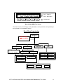
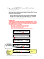
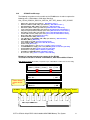
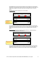
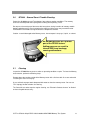
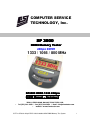
COMPUTER SERVICE
TECHNOLOGY, Inc.
SP 3000
DDR3 Memory Tester
240pin DIMM
1333 / 1066 / 800 MHz
SP3000 DDR3 1333 240pin
DIMM Manual – Revision 6
•
2336 LU FIELD ROAD, DALLAS, TEXAS 75229 USA
Tel (972) 241-2662 * Fax (972) 241-2661 * Email : [email protected]
•
website : www.simmtester.com
CST Inc SP3000 240pin DDR3 1333/1066/800 MHz DIMM Memory Test System
1
Table of Contents
Table of Contents
Warranty
General Safety
Notice
Page
2
5
5
5
1. Unpacking and Inspection
6
2. The SP3000 memory tester
2.1 SP3000 Product overview
2.2 Sp3000 System Hardware
2.3 Specification
7
7
8-9
10
3. Operating Basic
3.1 Configuration menu setting
3.2 Auto-ID Menu
3.3 File Menu
3.4 Edit Menu
3.5 Test Menu
3.6 Result Menu
3.7 File / Save / Delete Menu
11
13
18
19
19
26
27
28
4. Quick Guide with Examples
4.1 Auto ID an Unknown Device
4.2 Test a Known Device
4.3 Changing Test Parameters
4.4 Test a Device and Program SPD ~ All in one key punch function
4.5 How to set the Permanent SPD Write-protect and Reversible write protect
4.6 How to decode memory error on the SP3000
30
30
32
33
36
39
40
5.
43
43
45
46
47
SP3000 Basic Mainteance
5.1 General Cleaning
5.2 Replacing Worn Out Test Socket
5.3 Troubleshooting Guide
5.4 Tester Firmware Upgrade
CST Inc SP3000 240pin DDR3 1333/1066/800 MHz DIMM Memory Test System
2
Warranty
All components used in CST product are of the highest commercial grade available.
Furthermore, each product is subjected to a very rigid test program during and after
assembly and prior to shipment. Nevertheless, as with all components and equipment,
there could be a certain small percentage of failure.
CST, Inc. warrants for a period of one (1) year from the date of purchase by the original
customer, all products manufactured by it, to be free under normal use and service from
defects of material and workmanship. During this period, if the product unit is determined
to be defective, return it to your original place of purchase. They will promptly, at their
option, repair or replace the defective unit.
This warranty shall not apply to any consumable parts beyond its expected usable life
cycle specified in the specification section. This warranty shall not apply to any product
which has been repaired or altered in any manner by anyone other than CST, Inc., or
products which have been connected, installed, used or otherwise adjusted other than in
accordance with written instructions furnished by CST, Inc.
The above warranty shall not apply to defects resulting from improper or inadequate
maintenance by customer, or operation outside of the environmental specifications for
the products. The above warranty shall not be extended beyond its original term with
respect to any part or parts repaired or replaced by CST, Inc. No person, including any
dealer, agent or representative of CST, Inc. is authorized to assume for CST, Inc. any
obligation or liability other than expressly stated here. CST, Inc. does not assume any
liability for incidental, special and/or consequential damage of any kind whatsoever, and
in any event, liability shall in no case exceed the original price of the product.
Implied warranties, including, without limitation, warranties of merchantability or fitness,
are expressly limited in duration to the one- (1) year specified above. Certain terms and
conditions of the warranty may not apply where local laws prevail.
CST Inc SP3000 240pin DDR3 1333/1066/800 MHz DIMM Memory Test System
3
General Safety
Review the following safety precautions to avoid injury and prevent damage to
this product or any products connected to it. To avoid potential hazards, use the
product only as specified. Only qualified personnel should perform service
procedures
Injury Precautions
Use proper Power Cord
: To avoid fire hazard, use only the power cord
specified for this product
Avoid Electric Shock
: To avoid injury or loss of life, do not removed
front panel and try to retrieve any components
or try to fix any defects, without a qualified
personnel. Do remember to shut down any
power source, if products are under
maintenance.
Ground the Product
: This product is grounded through the
grounding conductor of the power cord. To
avoid electric shock, the grounding conductor
must be connected to earth ground. Before
making the connections to the input or output
terminals of the product, ensure that the
product is properly grounded
Do not operate without cover: To avoid electric shock or injury, do not
operate this product with safety covers or
panels removed.
Do not operate in Wet/Damp Conditions: To avoid electric shock, do not
operate this product in wet/damp conditions
CST Inc SP3000 240pin DDR3 1333/1066/800 MHz DIMM Memory Test System
4
Notice
Unless otherwise stated, the information contain in these documents are subject
to change without notice.
CST, Inc. MAKES NO WARRANTY OF ANY KIND WITH REGARDS TO THIS
MATERIAL, INCLUDING, BUT NOT LIMITED TO THE APPLIED WARRANTIES
OF MERCHANTABILITY AND FITNESS FOR A PARTICULAR PURPOSE.
CST, Inc. shall not be liable for errors contained herein or for the incidental or
consequential damages in connection with the furnishing, performance, or use of
this material.
CST, Inc. assumes no responsibility for the use or reliability of interconnected
equipment that is not furnished by CST, Inc.
This document contains proprietary information that is protected by copyright. All
rights are reserved. No part of this document may be photocopied, reproduced or
translated to another program language without prior written consent of CST, Inc.
The information contained herein has been prepared by CST, Inc. solely for use
by CST, Inc.’s employees, agents and customers. Dissemination of the
information and/or concepts contained herein to other parties is prohibited
without CST, Inc.’s prior written consent.
If you required further assistance with this product, please contact CST, Inc.
technical support hot line or authorised representative.
Technical Support
:
(972)-241-2662
USA
Hot-Line
Fax
Email
Website
:
:
:
(972)-241-2661
USA
[email protected]
www.simmtester.com
Copyright (c) 2011 by CST, Inc. All rights reserved.
CST Inc SP3000 240pin DDR3 1333/1066/800 MHz DIMM Memory Test System
5
1.
Unpacking and Inspection
Every precaution has been taken to ensure that the product reaches you in fully
operational condition. If there are any damaged to the packaging, or to the product, it
should be returned to the shipper and CST, Inc. should be notified immediately.
Upon unpacking, inspect the unit for any obvious physical damage, such as broken
display indicators, buttons and connectors, etc. If any damage is evident, return it to CST,
Inc. or to any authorized representative for repair or replacement. Please keep carton
box, foam packaging material and plastic bags in the event that the unit has to be
returned to CST.
Check missing
or damaged test
socket pins
Check for
missing button
caps
Check LCD for
cracks
CST Inc SP3000 240pin DDR3 1333/1066/800 MHz DIMM Memory Test System
6
2. The SP3000 Memory Tester
The SP3000 - is a new generation of Memory Testers from CST, Inc. It is built with state-ofthe-art technology to fit the memory testing needs of the computer service industry. The
compact, portable and stand-alone SP3000 with the proper optional adapters is capable of
testing the standard DRAM, page mode and EDO access mode 72 pin SIMM & 168 pin
SDRAM DIMM, with optional adapter it has ability to test DDR2,DDR1, SODIMM & PCMCIA
type of modules and many. All these tests are performed on the same base tester with
optional plug and Test Adapter. Designed with the service professionals in mind, and
coupled with the knowledge of the future memory market trends and demands, the SP3000
is the Memory Testers with the future built-in.
The automatic identification detection feature allows user to identify the module’s
configuration in seconds. Special settings are not needed, - just insert the module and press
a function key! The results include memory size; structure, type and speed are clearly
displayed on the LCD. The testers can also provide a group of standard test devices for you
to test with or if you prefer, you can customize your test and save it in the tester, so you
won’t lose the data even the tester is power down.
The SP3000 have been carefully planned and designed to be affordable while providing
maximum upgrade ability for today and tomorrow’s needs. Their modular expansion adapter
can accommodate future memory testing needs with ease at an affordable cost. At the same
time your investment in to the tester is protected from obsolescence.
The SP3000 is a cost-effective solution for service professionals especially in incoming
inspection, engineering, field service, depot support, system integrators, resellers,
system/subsystem manufacturers and any industry where memory is used.
2.1
SP3000 Product overview
Adapter Option :
SP3-240pin DDR2 DIMM –Adapter
LED Status
Indicator
LCD Display
Function Keys
CST Inc SP3000 240pin DDR3 1333/1066/800 MHz DIMM Memory Test System
7
Rear Panel
This chapter highlights the key features of the SP3000-DDR3 DIMM Tester. Hardware
and software are covered in this section.
2.2 System Hardware
Light weight, portable universal stand-alone memory tester.
• Easy to use.
• Uses a powerful & high speed Motorola micro-controller to manage the I/O task (such as
LCD Display, function keys, printer …etc).
• An allocated system storage space is used to save the test parameter, erasable and
programmable, data will not be lost even when the power is down.
• The interface to the device under test utilized sophisticated customized designed chips,
for easy error detection of problematic modules.
• 2 lines by 40 alphanumeric characters LCD display shows clear instructions and test
results.
• Test results can be printed to printer through the on-board parallel port.
• Optional PC interface kit enable testing through PC control software.
• 5 programmable function keys are included for all the menu options.
DDR2 Test Adapter Available:
• SP3-240pin DDR2 DIMM Adapter (1066/ 800 / 667 / 533/ 400 MHz)
• SP3-200pin DDR2 SODIMM Adapter (800/667/ 533 / 400 MHz)
• SP3-DDR2 BGA Chip Adapter (800/667/533/400Mhz)
• SP3-DDR2 BGA POGO Pin Chip Adapter (800/667/533/400Mhz)
DDR Test Adapter Available:
• SP3-184pin DDR DIMM Adapter (500 / 400 /333 / 266 / 200 MHz)
• SP3-184pin DDR DIMM Adapter (440 / 400 / 333 / 266 MHz)
• SP3-200pin DDR SODIMM Adapter (400/ 333/266/200 MHz)
• SP3- 66pin DDR TSOP Chip Adapter (333/266/200 MHz)
CST Inc SP3000 240pin DDR3 1333/1066/800 MHz DIMM Memory Test System
8
SDRAM Test Adapter Available:
• SP3-168pin SDRAM DIMM Adapter (133MHz Max)
• SP3-168/144 pin SDRAM DIMM/SODIMM Adapter (133MHz Max)
• SP3-100 pin SDRAM DIMM Adapter
Other Test Adapter Available:
• SP3-72/168 pin DRAM SIMM/DIMM Adapter
• SP3-30/72/168 pin DRAM SIMM/DIMM Adapter
• SP3- 144pin SGRAM Adapter
• SP3- 72/144pin DRAM SODIMM Adapter
• SP3-100pin DRAM DIMM Adapter
• SP3- Sun SPARC 200pin Adapter
• SP3-PCMCIA DRAM Card Adapter
SP3- DDR 400Mhz Adapter
SP3- DDR2 800 MHz Adapter
CST Inc SP3000 240pin DDR3 1333/1066/800 MHz DIMM Memory Test System
9
2.3 Specifications
Memory Type
240 Pin DDR3 DIMM SDRAM
Module Type
PC3-6400, PC2-8500 , PC3-10666
DIMM Pin-out
240pin Unbuffered DIMM & RDIMM
Module Density Limit
512, 1,2,4,8 & 16 GB
Test Clock Frequency
400,533 & 667mhz Clock , 5 mhz increment
Memory Data-Rate
800 ,1066 & 1333 Mhz
Address Depth
4 GB address field up to 16 row & 12 column
Data Bit Width
64 & 72
Control Lines
1-RAS, 1-CAS, 4-CS , 2-CKE, 9-DQS, 9-DQM
Variable Test Voltage
Vdd = 2.0, 1.9, 1.8 , 1.7, 1.6 , 1.5 1.4 & 1.35 V
Variable AC Parameters
CAS Read Latency = 5 ,6 ,7,8,9
TRCD = 5 ,6 ,7,8,9
TRP = 5 ,6 ,7,8,9
AL = 0,1,2,3,4
CAS Write Latency = 5,6,7,8,9
Refresh : 8 ,16,32 ,64 & 128 us (Self & CBR)
Test Pattern
Assembly Check : Walk Data , Walk Address , Chk_CS,
ChK_CKE, ChK_DQS, Chk_DQM, & SPD_Address Test.
Functional : Mat-S, Mar_X , Mar_C , Mar_Y , Mov-I
Programming : SPD Read , SPD Write, CRC
Checksum Auto calculation
Power Requirements
• Power Adapter :
Input 100 - 250Vac
Frequency - 50 - 60 Hz
Output - 12V @3A
Operating Temperature
• 32° F to 100° F ( 0° C to 60° C )
Physical Dimension
• L x W x H : 9.30” x 9.25” x 2.00” (236mm x 235mm x 51 mm)
• 6 lbs. ( 3 Kg )
CST Inc SP3000 240pin DDR3 1333/1066/800 MHz DIMM Memory Test System
10
3. Operating Basics
T
his chapter guides you through the SP3000 DDR3 test system basic menu operation. The
SP3-204-DDR3- SODIMM Adapter is required to be attached to the base SP3000 Tester for
DDR3 SODIMM Module Testing.
•
Unpack the tester from the box
•
Connect the DC Power adapter to the SP3000 Tester.
•
Plug-on the required Test Adapter to the SP3000 Tester.
•
Switch off “Power” before changing a different test adapter.
•
Turn on the Power Switch at the rear of the tester.
•
A Sign-On Message will be displayed on the LCD.
DDR3
Adapter
Adapter
Firmware
Vx.xx
DDR3
1333 MHz
CST Inc. SP3000 DDR3-1333 rev3.20- c1
[
•
] [ File ] [ Config ] [ SPD
FPGA
Version-xx
][ Auto ID ]
The SP3000 tester is ready for testing the DDR3 DIMM module!
CAUTION:
Ensure the Power is turned off before removing or
replacing Test Adapter or Test Socket.
If the above LCD screen message does not appear,
the adapter firmware may be corrupted
CST Inc SP3000 240pin DDR3 1333/1066/800 MHz DIMM Memory Test System
11
Line 1 - Sign-On
CST INC. SP3000 DDR3-1333 Rev3.20-c1
[
][ File ][Config ][ SPD ][ AutoID ]
ESC
F1
F3
F2
Line 2 - Main Menu
F4
Function Keys
Basic SP3000 DDR3 Test Screen
The 2nd line on the LCD display usually denoted as the key functions corresponding to
the key buttons in-line below the display.
Basic Menu Organization
Main Menu
NO Calibration
required for DDR3
Auto-ID. Menu
SPD
Config Menu
File Menu
Type :240 pin
800 , 1066 , 1333Mhz
Standard Devices
Test Menu
User Devices
Edit Menu
Read SPD
Edit SPD
Write SPD
Print SPD
Result Menu
ClrDev
Default
Auto ID
CST Inc SP3000 240pin DDR3 1333/1066/800 MHz DIMM Memory Test System
12
3.1
Configuration Menu setting
The [Config] Configuration menu allows selection for the following system
configuration setting:
System Configurations
[ Esc. ] [
] [ ClrDev ] [ Defaut ] [ Scroll ]
System Configurations
[ Esc. ] [ Comm ] [ Print ] [ Handlr ] [ Scroll
]
Selecting [Scroll] brings up this Menu
System Configurations
[ Esc. ] [
][
][
] [ AutoID ]
Default AutoID Settings:
[ Esc. ] [
][
][
SPD ] [ Patn ]
Return to Main Menu.
Press [ ClrDev ] key, bring up the Clear Device Menu [ Clears all stored device
file from SP3000 base tester.
Press [ Default ] key , bring up the Default setting Menu [ Clears ] previous
pattern setting and resets test pattern at factory setting – walk address, walk data
& mat-s]
Press [ Comm ] key, bring up the Com Port Menu. [ Set RS232
communication baud rates ]
Press [ Print ] key, bring up the Printer Menu. [ Select printer form feed format
when printer is connected directly to SP3000 printer port ]
Press [ Handlr ] key to bring up the Handler setting Menu [ Function to enable or
disable Handler mode, for manual testing ensure – Handler is turn OFF ]
Press [ Scroll ] key, to bring up the Default Auto-ID Setting Menu
3.1.1 Clear Device Menu.
This menu enable user to clear out previous old device library stored in the
SP3000 base tester, the SP3-DDR3 adapter enable user to create and store up
to 8 users define device library.
3.1.2 Default Menu.
This menu enable user to quickly restore test pattern setting including the burstlength to its factory default setting. When the default key is selected, the following
test pattern is set as a default:
- Walk address, Walk data . Mat_S,
CST Inc SP3000 240pin DDR3 1333/1066/800 MHz DIMM Memory Test System
13
3.1.3 Com Port Menu.
This menu enable user to redefine the baud rate between the PC and SP3000.
When user opt to use the PC to display the SP3000 screen output or for
performing a Firmware update, the SP3000 Tester can connected to any PC’s
Com port with the use of a Serial Cable. An Advanced PC software will be
required to communicate with the SP3000 tester
When [Comm] Menu is activated:
Baud rate = 19200
[ Esc. ] [
][
] [ Toggle ] [ OK
]
Press [ Esc. ] key, return to Main Menu.
Press [ Toggle ] key, edit the baud speed setting . Baud-rate setting available
are 19200, 9600, 4800 , 2400 & 1200.
Press [ OK ] key, return to the System Configuration menu
Factory default Baud Rate setting is 19200.
3.1.4 Print Menu.
The [Print ] function enable the selection of paper or form feed to the printer
connected.
Form Feed : Yes
[
][
][
][
F.F.
][
OK ]
[ F.F. ] key, toggles the Form Feed between Yes or No
[ OK ] key, return to the System Configuration menu
3.1.5 Handler Menu.
The [Handler] function allow the user to enable or disable the Handler control when
interface with any CST ‘s RoboFlex2 Automatic Handler System.
Handler : Off , Sort : 1000 ms
[ On ] [ --- ] [ + 1 s ] [ + .1s ] [
OK ]
3.1.6 Default Auto-Id Settings :
The [ Default Auto ID Settings ] function enable user to pre-select the default test
patterns during the Auto-ID stage. The default test pattern can be used, when the
selected test pattern is activated. The user may edit the default test pattern by using
the Edit function key for that particular test routine.
Default AutoId Settings :
[ Esc. ] [
][
[
Esc ]
] [ SPD ] [ Patn ]
- Returns to System Configuration menu
CST Inc SP3000 240pin DDR3 1333/1066/800 MHz DIMM Memory Test System
14
[ Patn ]
- The [ Patn ] or Pattern function brings out the following test patterns
which user can define as defaults test patterns to be used whenever a
module is selected to be Auto-ID or tested.
WA+WD+Mt+
[ Esc ] [ Basic ] [ Custom ] [ Burst ] [
]
[ Basic ] - The Basic function select only Walk Address and Walk Data default
test. This is the quickest test ( 2 seconds) for checking opens and shorts.
Basic test checks for assembly problem and may not capture DRAM cell
problems
[ Burst ] - The Burst function enable user to select the burst type [ Sequential or
Interleave mode ] and burst length [ 4 & 8 ]. Setting the burst length with
8 will speed up the test time.
[ Custom ]- The custom function brings out the following test patterns which user
can select as default. Custom pattern setting can be saved in either the
SP3000 base tester or transfer to PC for storage and recall later for
testing
[ x ]w_Addr [ x ]w_Data [ x ]MatS
[ Toggle ] [ <-- ] [ --> ] [
OK
]
[ ] Mar_x [ ] Mar_C [ ] Mar_Y [ ] MovI
[ Toggle ] [ <-- ] [ --> ] [ OK ]
[ ] chk_CS [ ] chk_CKE [ ] chk_DQM [ ]
[ Toggle ] [ <-- ] [ --> ] [ OK
]
[ ]spdRC [ ]spd_addr [ ]
[ Toggle ] [ <-- ] [
]
--> ] [
OK
For Assembly Checks
•
W_data : Walk Data pattern are used to detect shorts in the Data lines of the
module.
•
W_addr : Walk Address pattern are used to detect shorts on the address lines of
the SODIMM module including BA 0 and BA1.
•
Chk_C.S: Chip Select are used to check for assembly shorts and open on the
four CS pins ( CS 0 ,1,2 & 3) of the DIMM module.
•
Chk_CKE : CKE test are to use to check for open and short of CKE0 and CKE1
on the DIMM module.
CST Inc SP3000 240pin DDR3 1333/1066/800 MHz DIMM Memory Test System
15
•
Chk_DQM : DQM test are to used to check for open and short on the 9 DQM pin
( DQM 0 – 8) on the DIMM module
•
Check SPD_Addr : SPD Address Test are used to check for shorts and open
on SDA 0,1,2
For Functional Test
The following abbreviations are types of functional failures below:
AF – address decoder fault
B – number of bits (cells) in the memory word
CF – coupling faults
CFdyn – dynamic CF
CFid – idempotent CF
CFin– inversion CF
SAF – stuck at fault
SCF – state coupling fault
TF – transition fault
W – write operation
•
Mar_S Test : (Modified Algorithmic Test Sequence +), is a short test that
detects all unlinked SAFs and AFs failures.
•
Mar_X Test : This March X test is used to test for Cfins , Afs, SAFs and TFs
not linked with Cfins.
•
Mar_C Test : This March C test is used to test for unlinked CFins , Cfids,
Cfdyns, Afs, SAFs and TFs.
•
Mar_Y Test : This March Y test is used to test for linked CFins, , Afs, SAFs
and TFs linked with CFins.
•
Mov_I Test : This Moving Inversion test is used to test for unlinked Cfids,
Afs, SAFs,TFs.
For SPD Read and Write Test
•
SPD_RC : SPD Read Data Test runs the SPD test based on the
configuration defined in the SPD menu. Byte 0-255 from SPD EEPROM
is compared with SPD Data stored in Buffer. The SPD test can be
executed in the same cycle after the rest of the test pattern is completed
when activated.
•
SPD_WRC : SPD Write and compare Data Test – writes data into Byte 0-255
on the DIMM Blank SPD EEPROM and compared with SPD Data stored
in Buffer. When SODIMM SPD EEPROM does not match Buffer Data ,
tester will fail SPD Data test. The SPD test can be executed in the same
cycle after the rest of the test pattern is completed when activated.
•
SPD CRC Checksum calculation ( Byte 126-127) is offered as a standard
feature for DDR3 SPD programming.
CST Inc SP3000 240pin DDR3 1333/1066/800 MHz DIMM Memory Test System
16
3.1.7 SPD Setting ( Default)
[ SPD
]
- The [ SPD ] function are used for the following SPD setting which user
can define as defaults SPD parameters to be used whenever a module is
selected to be programmed.
Default Auto-Id Settings :
[ Esc. ] [
][
] [ SPD ] [ Patn
]
Press [ SPD. ] key, return to change SPD setting
WRT Page Length = 4
[ Esc. ] [
][ ][
][
OK
]
Press [ ----> ] key, to change the Write Page length setting to : 1, 4, 8 & 16 bytes
Page length setting is dependent on the specification of the
EEPROM. SPD Programming time can be speed up with a higher
byte length setting, check the EEPROM manufacturer specification to
determine the appropriate page length setting. CST recommends
Page Length 4 to support most EEPROM.
Press [ ----> ] key, to Specify SPD Read/Write Range [ Typical 0 –255]
SPD Read : 000 => 255
[ Esc. ] [ Toggle ] [ ] [ ] [ OK
]
SPD Write : 000 => 255
[ Esc. ] [ Toggle ] [ <----- ] [ ------>][ OK
]
Press [ ----> ] key, to Mask Out Byte 120 - 125 which is used for programming
serial number and date codes. This bytes are unique number and ignore during SPD
data comparing.
Mask Out Byte 120-125 ? : Yes
[ Esc. ] [
][
] [ No
][ OK
]
Read Cmp : enable user to compare SPD data with the SPD data saved in the file or
from the SP3000 tester buffer, NO SPD rewrite is possible for this mode selection.
SPD_Data_Test allowed: RD_Cmp
[ Esc. ] [
] [ <----- ] [ ----> ][
OK
]
WR Cmp : Allow user to compare SPD data with the SPD data saved in the tester's
buffer, and allow SPD rewrite after passing all functional test. Be careful when
CST Inc SP3000 240pin DDR3 1333/1066/800 MHz DIMM Memory Test System
17
selecting this function. The original SPD data from the DIMM EEPROM will be
overwritten.
SPD_Data_Test allowed: WR_Cmp
[ Esc. ] [
] [ <----- ] [ ---->
] [ OK
]
For permanent & reversible write protect setting, read chapter 4. 5 page 39 for
details
3.2 Auto ID Menu
The automatic identifying (Auto-ID) device functions, allow user to determine the
configuration, size, speed…… etc of the unknown module under test. The following
parameters will be determined:
•
•
•
•
•
•
Device Operating Voltage – VDD: 1.5V
Rows configuration
Columns configuration
Number of data lines
Number of banks ( Internal & external )
Access time
3.2.1 From the main menu, once the Auto I.D function is activated, the Module Type
menu and the Clock Frequency menu will display allowing User to select the desired
Data-Rate Frequency of 800 ,1066 or 1333 MHz to test the module. The tester will
sense if the EEPROM has SPD data written, this menu selection will appear.
Select Data Rate :
[ 800 ] [ 1066 ] [ 1333 ]
3.2.2 Once the 1066 MHz Data-rate frequency is selected, it takes about 3 –6 seconds to
identify the SODIMM module depending on device type and configuration.
Identifying the Device ………..
[ 00:03 ]
3.2.3 If a known good module is detected, the SP3000 LCD will display the following
parameters
DDR3 64Mx64 512MB 1B(8)@2x533Mhz 1.5V
[ Esc. ] [ Edit ] [
] [ Defset ] [ Test ]
Press [ Edit ] key, bring up the Edit Menu.
Press [ Test ] key, bring up the Test Menu.
Press [ Esc. ] key, return to Main Menu.
Press [ -Defset] key, to reset all test pattern to factory default value [ Walk Data,
Walk address, Mat-S ]
CST Inc SP3000 240pin DDR3 1333/1066/800 MHz DIMM Memory Test System
18
3.2.4 If a defective/bad module is detected, an error message will be prompted:
Occasionally this can be due to bad contacts of modules with the test sockets. If this
happens, remove and re-insert the DIMM module firmly and press the [ Auto ID ] to
retest again. EDO/FPM standard DRAM or SDRAM module will not fit into the DDR3
Adapter the "Cannot Identify Device" will be prompted as shown below.
Cannot Identify Device.
[ Esc. ] [
][
][
] [ Auto ID ]
3.3 File Menu
For verifying a known memory module, the following menu should be selected. The
following display contains only 2 standard device with predefined - BASIC test. The
SP3000 tester allows up to a limited 8 customized test parameters to be saved. For more
storage device file selection, the SP3000 Advanced PC software offers more device
selection. Please check with CST customer support for a copy of the PC software.
Std. Dev. - 2, User Saved Dev. - 0
[ Esc. ] [ Std. ] [ User ] [
After
][
]
[ Std. ] or [ User ] key is pressed:
1>DDR3 128M x 64 1024MB 2B(8) @ 2x533Mz
[ Esc. ] [ Edit ] [
] [ Next ][ Test
]
For
[ Edit ] function, refer to section 3.4 Edit Menu.
Press
[ Next ] function scroll to Next device file.
For
[ Test ] function refer to section 3.4 Test Menu.
Press
[ Esc. ] key return to Main Men
3.4 Edit Menu
This menu allows users to modify the test parameters and test patterns.
There are two buttons that are use throughout the Edit Menu:
[Scroll] - the extreme right button, allows for page scroll to next screen which
show more parameters.
[ Esc. ] - the left button, when depressed returns back to previous menu
Edit Menu 1:
DDR3 128Mx64 1024MB 1B(8) @ 2x533Mz
[ Esc. ] [ AdrDat ] [ BnkCtl ] [ Pattn ] [Scroll ]
CST Inc SP3000 240pin DDR3 1333/1066/800 MHz DIMM Memory Test System
19
[AdrDat] - to edit Address/Data Paramters
[BnkCtl] - to edit Bank Control Parameters
[ Pattn ] - to edit Test Pattern/Preheat /Loop Parameters
Edit Menu 2:
DDR3 128Mx64 1024MB 1B(8) @ 2x533Mz
[ Esc. ] [ Volt ] [ Timing ] [ SPD ] [ Scroll ]
[ Volt ]
- to edit V.d.d. and Bouncing
[Timing ] - to edit ClK Frequency ,Refresh & Delays Parameters
[ SPD ] - to edit SPD setting
Edit Menu 3:
DDR3 128Mx64 1024MB 1B(8) @ 2x 533 Mz
[ Esc. ] [ F-Name ] [ P-Heat ] [ Type ] [ Scroll ]
[F-Name] - Set File Name.
[P-Heat ]
- Pre Heat
[ Type ]
- Select or Disable Registered Module
Edit Menu 4
DDR3 128Mx64 1024MB 1B (8) @ 2x533Mz
[ Esc. ] [
][
] [ S.O. E ] [ Scroll ]
[ S.O.E ]
- Stop on first Error
3.4.1 [ Addr Data ] Address/Data Sub-Menu.
This menu allowed users to redefine the parameters on:
Blinking Cursor - Indicate that current
editing parameter. Eg. Row
Row:14¦ Col:10 Data:64 Banks:2 (8)_
[ - ] [ + ] [ -> ] [ OK
]
Address Setting - Number of Rows, Number of Columns, Number of Banks.
Number of Data Bits
[ - ]
[ + ]
[ -> ]
- Hold down and decrement the current parameter by 1.
- Hold down and increment the current parameter by 1
- Point to next parameter.
When the cursor is at Bank item, continuous pressing will bring the cursor back to the
Row Item
CST Inc SP3000 240pin DDR3 1333/1066/800 MHz DIMM Memory Test System
20
Note :
• The program will perform range checking on the current
parameter.
• If the value is below the range, it will roll to the higher value.
• If the value exceeds the range, it will roll to the lowest value.
• For ‘Row’ and ‘Col.’, Range is between 8 and 16.
• For ‘Data’, Range is between 1 and 72.
• For ‘Banks’ , Range is between 1 and 4.
• All DDR3 Chip has 8 internal banks
3.4.2 [ Bank Ctl ]Bank Control Sub-Menu.
♦
♦
♦
♦
This menu enables changes for the RAS and CAS control signals of each bank
The program will first display the RAS Control Menu , then followed by the CAS Control
Menu.
If the module has more than 1 bank, the program repeatedly shows the RAS Control
and CAS Control Menus until last bank has been modified.
When a CS is enabled, the LCD Display will show a [ _ ] enclosing the number;
otherwise, it is disabled.
Bank No. : Total Number of
Banks
CS Control Menu:
S: [ 0 ] 1 2
3
Bank: 1
[ Esc ] [ Toggle ] [ <----- ] [ ---> ] [ OK ]
[Toggle] - Enable or Disable the current Chip select setting. [ x ] indicates enable.
[
->
] - Rotate the underlined cursor to next CS selection.
[ OK ] - complete the changes.
CKE Control Menu:
CKE: [0] 1
Bank:
1
[ Esc ] [ Toggle ] [ <--- ] [ -----> ] [ OK ]
[Toggle] - Enable or Disable the current CKE setting.
[
->
] - Rotate the underlined cursor to next CKE .
[ OK ] - complete the changes.
DQS – Data Strobe Control Menu:
DQM : [0][1][2][3] [4] [5][6] [7] [ 8]
[ Esc ] [ Toggle ] [ <----- ] [ -----> ][
Bank:1
OK ]
CST Inc SP3000 240pin DDR3 1333/1066/800 MHz DIMM Memory Test System
21
[Toggle] - Enable or Disable the current DQS setting.
[
->
] - Rotate the underlined cursor to next DQS.
[ OK ] - complete the changes.
DQM Control Menu: (Data Mask Enable)
Module with DM 0-8 controls
[Toggle ][
OK
]
DM : [ 0][ 1] [ 2] [ 3] [4 ] [ 5] [6 ] [ 7] [ 8] Bk:1
[ Esc ] [ Toggle ] [ <---- ] [ -----> ] [ OK ]
3.4.3 SPD . Sub-Menu.
The Serial Present Detect (S.P.D.) is used by DIMM Memory manufacturer to indicate
the configuration, speed and some other specifications. It is done so by selectively
programming the serial EEPROM on the DIMM modules.
000 : 80 08 08 0E 0A 50 40 07 08 09 0A 0B
[ Scroll ] [ Saved ] [ Config ] [ Read ] [ OK ]
[ Saved ] - Accept the read SPD information and save to Tester Buffer
[ Config ] - Change SPD parameters.
[ Read ] - Read SPD data from module's EEPROM inserted on the DUT.
[ O.K. ]
- Accept the changes made in this menu and return to previous menu.
[ Scroll ] - Go to next page of SPD setting menu
000 : 00 01 02 03 04 05 06 07 08 09 0A 0B
[ Scroll ] [W->DUT ] [ Edit ] [
] [ Ok ]
[ W->DUT ] - Write SPD Data from into SPD EEPROM into Device Under Test
[ Edit
]
- Edit SPD data – enable user to scroll byte by byte to edit SPD data
in Hex format
000 : 00 01 02 03 04 05 06 07 08 09 0A 0B
[ Scroll ][ Prnt ] [
] [ SetSWP ][ ClrSWP ]
B 000 : Number of Bytes Written
80 h
[ OK ] [ >> ] [ Toggle ] [ Back ] [ Next ]
[
>>
] - Double arrow enables user select which two hex digit to edit
[ Toggle ] - Toggle enable user to set Hex number
[ Back ] [ Next ]- Back & Next key - to scroll forward or backwards to select byte
CST Inc SP3000 240pin DDR3 1333/1066/800 MHz DIMM Memory Test System
22
000 : 00 01 02 03 04 05 06 07 08 09 0A 0B
[ Scroll ] [ Prnt ]
[ Prnt ]
- sent to Print SPD content from the tester buffer
3.4.4 [ Volt ] D.C. Voltage Parameters Sub-Menu.
When testing any module an upper or lower voltage limits are necessary.
The VCC. voltage setting in this menu allows user to perform this task.
3 test voltages are selectable:
• For 1.5V Module, Voltage adjustable are 1.4V, 1.5V and 1.6V
The software Bouncing option when enable, permits voltage cycling
eg. for 1.6 V device
1.6
1.5
1.4
[ Vcc ]
- 3 Voltage settings for selection.
1.4V -> 1.5V -> 1.6V
Vcc : 1.5 V Bounce - No
[ Vdd. ][Bounce][ OK ]
[Bounce]
- Voltage Bouncing Yes or No.
3.4.5 [ Timing ] Clk Frequency /Refresh Parameters Sub-Menu.
CLK : 400 Mhz
[ Clk Frq ] [ MR0 ][ MR1 ][ MR2
][ OK
]
Clock Frequency (MHZ) : 400
[ ESC ] [
][ ][
][ OK
]
•
•
•
•
Clock Frequency can be preset from 400 ~ 670 MHz in steps of 5Mhz
[ MR0 ] Mode Register Set for setting CAS Latency, Trcd, Trp & Write Latency
[ MR1 ] Extended Mode Register Set for setting Output D.I.C, ODT resistor
value.
[ MR2 ] Extended Mode Register Set for setting CAS Write Length, Refresh
rate, MPR, Disable ODT)
CST Inc SP3000 240pin DDR3 1333/1066/800 MHz DIMM Memory Test System
23
For MRS0 Setting ( Mode Register Set)
CL: 7 Wr:7 Trcd : 7 Trp : 7
[ CasLat ] [ WR ] [ Trcd ][ Trp ][ OK
]
Most DDR3 1066Mhz DIMM are preset with (CL=7, WR=7, T RCD=7 , TRP 7)
setting. This setting is programmed into the DIMM SPD.
CL Read Latency can be preset to – 5,6 ( 800 ) 7,8 ( 1066Mhz) ,7,8,9 (
1333Mhz)
WR : Write Recovery Precharge can be change from 5, 6,7,8. Changing the
WR setting does not affect test time
Trcd is the time delay between the Row and column address – you can select
either 5,6 ,7,8, 9 Clock
T rp is the Auto Pre-charge time, DDR3 SDRAM internally generates the
timing to satisfy Tras for the programmed burst length and CAS latency, you
can select either 5,6,7,8, 9 Clock
•
•
•
•
For MRS1 Setting ( Extended Mode Register 1 Set)
ODT : 40 ohm Output DIC : 34 ohm
[
][
] [ ODT ][ D.I.C
][ OK
]
The MRS1 setting offer in the SP3000 DDR3 tester, are for advanced users.
Always used the default value.
•
•
ODT : stands for On-Die-Termination , is a feature that allows a DRAM to
turn on/off termination resistance for each DQ,DQS,RDQS and DM Signal
via the ODT control. The ODT feature is designed to improve signal integrity
of the memory channel by allowing the DRAM controller to independently
turn on/off termination resistance for any or all dram devices. In the SP3000,
user can select 20,30,40, 60ohm or 120ohm or disable the termination
resistor
[ Output D.I.C ] – Driver Impedance Control.. user can select 34,40 ohm
For MRS2 Setting ( Extended Mode Register 1 Set)
DODT: Off
CAS_WL:5 Refresh
[ DODT ][Cas_WL ][ Refresh }
[ OK ]
[ DODT ] – Dynamic ODT Control.. user can select off ,60,120 ohm
[ CAS_WL ] – Write Latency user can select off 5,6,7 and 8 Clock
[ Refresh ] - Change the type of refresh
2 types of Refresh are used -
no refresh & CAS before RAS (CBR)
CST Inc SP3000 240pin DDR3 1333/1066/800 MHz DIMM Memory Test System
24
Refresh Periods can be preset to - 8, 16, 32, 64 or 128 us per row.
• None (No) Refresh
• CBR (C.A.S. Before R.A.S.) Refresh
[ Period ] - Change the Refresh Period. Period (us/row) - 8, 16, 32, 64, 128
3.4.6 [ Pattn ] Test Pattern/Preheat/Loop Parameters Sub-Menu.
The SP3000 utilizes the fast testing time approach to uncover any assembly
errors and memory cell failures.
They are built with very fast tests time for high throughput and will provide over
99.5% confidence level on accuracy.
The user friendly selectable tests options are:
•
•
•
•
•
•
•
•
•
•
•
•
Walk Data test [ w_data ]
Walk Address test [ w_addr ]
Mat + S [ Marching ]
March_C
March_X
March-Y
Moving Inversion
Chip Select Test [ c.s. ]
CKE Test [ CKE ]
DQM Test [ DQM ]
S.P.D. Data Test. [ SPDDAT ]
S.P.D. Address Test [ SPDADR ]
When the Test Pattern is activated, the following will be display:
Test:adr+dat+mar+
[ Esc. ] [ Basic ] [ Custom ] [
Page L001
] [ Loop ]
[Basic ] - a quick key to switch to default patterns and default to 1 test loop.
- default test pattern to w_adr + w_dat + mar+.
[Custom] - User selectable test pattern:
[x]w_addr
[x]w_data
[x]Mat-S [ ] Mat_X
[ Toggle] [ <- ] [ -> ] [ OK ]
[ ] Mar_C [ ]chk_CS [ ]chk_CKE [ ] chk_DQM
[Toggle] [ <- ] [ -> ] [ OK ]
[
] spdRC [
] spaddr
[Toggle] [
[Toggle]
[ OK ]
[ Loop ]
<- ] [ -> ] [ OK ]
- Toggle the check-box ‘[x]’ or ‘[ ]’
[x] - enabled
[ ] - disabled
- Move the cursor to next menu item
- Test Loop Configuration:
Range between 1 and 999.
CST Inc SP3000 240pin DDR3 1333/1066/800 MHz DIMM Memory Test System
25
Test Loop : 001
[ Esc ] [ Toggle ] [
<-- ] [
--> ] [ OK
]
[ <-- ]- Toggle key and increment by 1
[ --> ]- Toggle key and increment by 1.
Setting Test Loop to : 000 will set the tester into a continuous burn-in loop.
3.4.7 Set File Name Menu
Allow the user to alter the name of the file:
Range of Characters - ‘0’ to ‘9’ and ‘A’ to ‘Z’
File Name : DEMO____
[
- ] [ + ] [ -> ] [ OK ]
[ - ] - Hold down and decrement the character.
[ + ] - Hold down and increment the character.
[ -> ] - Rotate the underline cursor to next position.
3.4.8 Stop-On-Error Menu
Default is STOP_ON_ERROR enabled, so that during testing, first error
encounter will stop the test immediately and print the result.
3.5 Test Menu
This menu is assigned as the Auto-ID or File Menu. When the user presses the [ Test ]
Key, The SP3000 will perform an ICC current measurement check before starting test
and the display message will be as follows.
L001: ICC Current
[Cancel]
[ 00:01 ]
|--Elapsed Time--|
L001: Walk Address
[ Cancel ]
[00:05]
If no modules are present on the SP3000 Test socket , the tester will prompt an failure
message on the display screen and it is as follows.
** Fail : wk_addr @ 2x 533Mhz , L1 ** [00:01]
[ Esc ] [
][
][
] [ Test ]
During the testing, any errors detected during testing will be aborted immediately and the
FAIL message will be displayed. Otherwise if no errors are detected, upon completion of
the defined tests, a PASS message will be displayed.
CST Inc SP3000 240pin DDR3 1333/1066/800 MHz DIMM Memory Test System
26
3.6 Result Menu
After completing all the defined tests with no errors detected, the LCD will display as
follow:
** PASS ** @ 2x533 Mhz L001 *
[ 00:08 ]
[ Esc. ] [ Result ] [ Print ] [ View
] [Result] - Check Pass Results
] [ Test
[ Print ] - Print Pass Results.
[ Test ] - Test Function.
[ Esc. ]
- Return Previous Menu
If an error is detected, the tester will display the following message:
** FAIL - Walk_Data, L1 **
[ 00:08 ]
[Result]
- Check
Result ] [ View ] [ Test ]
[ Esc.
] [ Result
] [ Print
[Print ]
- Print Error Results.
[ View ] - View the Error Details.
[ Esc. ] - Return Previous Menu.
3.6.1 View Error Details
A. When module “Failed” any test parameter, the following results will be displayed
and view function is selected
B. If the LCD cannot fully display all the failure bits on one screen or multiple banks
have errors, the
-
[ More ] key will appear for more data to be displayed by pressing this key.
:1, 2, 3, 4, 5, 6, 7, 8, 17-19, 35, 39, 49-51, 56-58, 68
* Bank 1*
[ More ]
- The final screen display will indicate an [ OK ] key to show the last page. Pressing the
key will return you to the previous menu.
CST Inc SP3000 240pin DDR3 1333/1066/800 MHz DIMM Memory Test System
27
3.6.2 Print Error Results
The [Print] function allows the user to output Error Results to the printer.
A sample printout can be seen as follows:
CST Inc SP3000 DDR3 – 1333 Mhz Rev x 3.03x
~~~~~~~~~~~~~~~~~~~~~~~~~~~~~~~~~~~~~~~~~~
Module : DDR3 128Mx64 1GB 1B (8) 2x533mhz 1.5V
Addr. ( row x col. ) : 14 x 10
Data (bank x bit)
: 1 x 64
Internal Bank
:8
Test Pattern
: w_addr, w_data, mt-s,
Loop #
:1
## FAIL : Walk Data - Loop 1 ##
Bank 1 : 1, 3, 5, 7, 9, 11, 13, 15, 17, 19, 21, 23, 27, 29, 31-32
Elapsed Time : 00:00:04
3.6.3 Check Result
This menu allows user to check back which test has passed or failed.
Pass: dat, adr
Fail: mat+
[
OK
]
3.7 File Save/Delete Menu
3.7.1 Save File
After Auto-Identifying a new device and pressing [ ESC ] to return to the main
menu , or Editing an existing device and pressing [ ESC ] to return to the main
menu.. The tester will prompt you to the following message:
Do you want to save this file?
[ F-Name ] [ No
[F-Name]
[ Yes
]
] [ Yes
]
- Place a 8-char. file name for further reference.
You can also access from Edit-Menu 3.
- Save file.
Maximum 8 files allowable to be saved, if files exceeds then the following prompt
will appear, It you press [Yes]
Files Full !!! Delete old files ?
[ No
[
No
]
] [ Yes ]
- Abort Saving.
CST Inc SP3000 240pin DDR3 1333/1066/800 MHz DIMM Memory Test System
28
3.7.2 Delete File
This menu is accessible from the user saved file menu - Option [ Del. ]
When Auto-ID a new device and pressing [ ESC ] to save the device and the
maximum device is exceeded, then the tester will automatically prompt you the
following menu:
5>DDR3 128Mx64 1GB 1B(4) @2x533Mhz #1.5V
[ Done ] [ Delete ] [ Next ]
[ Done ]
[ Delete]
- exit the delete menu.
- Delete the current selected file.
Confirm to delete file ?
[ No
] [ Yes
]
[ No ] - Abort Delete
[ Yes ] - Confirm Delete
[ Next ] - Advance to next file.
CST Inc SP3000 240pin DDR3 1333/1066/800 MHz DIMM Memory Test System
29
4. Quick Testing Guide with Examples
T
his chapter will guide you through a simple example with a known DDR3 DIMM module to
help you get familiar with the SP3000 DDR3 functions. If you should have any doubt on the
menu options, please refer back to the previous chapter on operations basics for a detailed
explanation.
The examples illustrated in this section use a standard 240pin 128Mb x 64 DDR3 DIMM memory
module. The device attributes are as follows:
•
•
•
Voltage.
Row x Col.
Data Bit x External Bank x Internal Bank
:1.5V
:14x 10 ( 1 bank)
: 64 x 1 ( 8 )
4.1 Auto ID an Unknown Device (No SPD Programming)
Assume device type is unknown (in this example, 128Mx64 is used), an Auto-ID function is
carried out to determine the memory device attribute. The BASIC test is performed to
determine if the module is good or bad. So lets run through the steps:
Step 1:
Insert the unknown DDR3 DIMM device into the test socket. The main menu
screen will display as follows:
CST Inc. SP3000 DDR3 1333 Mhz Rev 3.xx--xx
[
] [ File ] [ Config ] [ SPD
][ AutoID ]
Step 2:
Select [ Auto-ID ] and you will be prompted the following menu
Make your selection according to Data-rate required to test the module at [ select
400 , 533 & 667 Mhz if you are unsure] :
Select Clock Frequency :
[ 800 ] [ 1066 ] [ 1333 ]
Wait for a few seconds,
Identifying the Device …..
[ 00:03 ]
Step 3: Compare the device attributes shown on the LCD Display with your known
device attributes. 1GB DDR3 DIMM @ 1066Mhz
DDR3 128Mx64 1GB 1B(8) @2x 533 Mhz 1.5V
[ Esc. ] [ Edit ] [
] [ Defset
] [ Test ]
CST Inc SP3000 240pin DDR3 1333/1066/800 MHz DIMM Memory Test System
30
Indication of Device are as follows :
♦
DDR3 :
Double-Data-rate DIMM
♦
128Mx64:
Address base x Data Bit configuration of module
♦
1GB
:
Memory Size
♦
1B
:
External Bank …….. eg One external bank
♦
(8)
:
Internal Bank ……....eg Eight internal bank
♦
Vdd
:
Vdd voltage …………eg 1.5V
Step 4: Press
[ Test ] to perform the BASIC Test.
Check for ICC
over current
L001: ICC Current
[Cancel]
[00:01]
L001: Walk Data
[Cancel]
[00:02]
Check for Data bit
problem
L001: Mt+
[Cancel]
[00:03 ]
Check for
functional error
[ 00:05 ]
Test ]
Final test results
** PASS - L001 **@2x 533Mhz
[ Esc. ][ Result ][ Print ][
][
Step 5:
Press
[Result] to view the individual pass/fail test result.
Step 6 :
Press [ Print ] to print a copy of the individual test result
Step 6 :
Press [Esc] twice to return to the main menu.
Before reaching the main menu, the tester will prompt you to save the new
device detected.
Do you want to save this file?
[ Cancel ] [ F-Name ][
No
Step 7 :
Press [ No] and return to main menu.
Step 8 :
End of example.
][ Yes
]
CST Inc SP3000 240pin DDR3 1333/1066/800 MHz DIMM Memory Test System
31
4.2 Testing a Known Device with Stored File ( No Programming SPD)
To perform a test on a known standard device:
Step 1 : Insert the known device in the test socket.
Step 2 : Select
[ File ] Menu.
CST Inc. SP3000 DDR3 –1333 Mhz Rev 3.20-87
[
] [ File ] [ Config ] [ SPD ] [ AutoID ]
Step 3 : A next menu will prompt you to select [ Std ] Device or [ User Saved ] Device
Std. Dev. – 1 , User Saved Dev. - 5
[ Main ] [ Std. ] [ User ]
Step 4 :
Check for correct
device setting
Choose [ User ] for the standard device file.
Use [ Next ] to scroll to the next Device.
[1] DDR3 128Mx 64 1GB 1B(8)@2x533Mhz 1.5V
[ Esc. ] [ Edit ] [
][ Next ] [ Test ]
Step 5 :
Press [ Test ] to start the testing.
If module under test fails, the LCD will display :
** FAIL - Walk data, @2x533Mhz L001 ** [00:03]
[ Esc. ] [ Result ] [ Print ] [ View ] [ Test ]
Check for Data bit
problem
Step 6 : Press [ View ] to see the error in detail.
Press [ OK ] to return previous LCD display.
:12, 17-19
* Bank 1*
Data-bit failures
[ O.K. ]
Results indicates Module Fail Bank 1 , Data-bit DB12, DB17-19.
Step 7 : If a printer is connected, press [ Print ] to print the error results.
Step 8 : Press [ Esc ] twice to the main menu.
Step 9 : End of example.
CST Inc SP3000 240pin DDR3 1333/1066/800 MHz DIMM Memory Test System
32
4.3 Changing Test Parameters
Whenever the [ Auto ID ] or [ File ] options is selected,
The Test Parameters can be changed by selecting the [ Edit ] key.
This section illustrates how to activate the MAT-S test, and change the Operating Voltage
- Vdd to either 1.4V - 1.5V - 1.6V, and activate Chk_CS and Chk_DQM test
Step 1
:
Select [ File ] Menu, then
[ Std ] to standard device.
Use
[ Next ] Key to scroll to DDR3 128Mx64 device.
Press [ Edit ] to edit the device
1>DDR3 128Mx64 1GB1b(8)@2x533Mhz 1.5V
[ Esc. ] [ Edit ] [
] [ Next ] [ Test ]
Step 2
:
Press
[ Edit ] for more parameter options.
1>DDR3 128Mx64 1GB 1B(8)@2x533Mhz 1.5V
[ Esc. ] [ AdrDat ] [ BnkCtl ] [ Pattn. ] [ Scroll ]
Step 3
:
Press
[ Scroll ] for more parameter options
1>DDR3 128Mx64 1GB 1B(8) @2x533Mhz 1.5V
[ Esc. ] [ Volt ] [ Timing ] [ SPD . ] [ Scroll ]
][Scroll]
1>DDR3 128Mx64 1 GB 1B(8)@2x 533Mhz 1.5V
[ Esc. ] [ F-Name ] [ P-Heat ] [ Type ] [ Scroll ]
][Scroll]
Step 4
:
Choose [ Volt ] to edit VDD
Vdd : 1.5V Bounce - No
[ Vdd ] [ Bounce ] [
Step 5
:
OK
]
Toggle [Vcc] until 1.6V is displayed, press [OK] to return to previous menu
1>DDR3 128Mx64 1GB 1B(8) @2x533Mhz 1.6V
[ Esc. ] [ Volt ] [ Timing ] [ Pattn ][ Scroll ]
Step 6
:
Select [ Pattn ], to enter into the Test Pattern Menu,
Test: adr+dat+mt+
[ Esc. ] [ Basic ] [ Custom ] [
| Page|L001
] [ Loop ]
CST Inc SP3000 240pin DDR3 1333/1066/800 MHz DIMM Memory Test System
33
Step 7
:
You can either choose to change the pattern from the [ Basic ] function (for
quick setup) or from the [ Custom ] function (for detail setup).
Select [ Basic ] to view test pattern setup,
Press [ Mat+] toggles between [+March ] or [Basic ]
Test :wD+wA
[ Esc ] [ +Mat ] [ Custom ] [
Step 8
:
] [ Loop ]
Select [Custom] to customize the test pattern.
Test:adr+dat+mt
[ Esc. ] [ Basic ] [ Custom ] [
Step 9
:
Use
press
[ -> ] [ <- ] key to scroll cursor to [ ]Mt+
[Toggle] to active test. The [ x ]Mt= will appear marked to indicate
[x]w_addr
Step 10 :
press
press
The
L001
] [ Loop ]
[x]w_data
[x]mt [ ] Mar_X
[ Toggle ] [ <- ] [ -> ] [ OK
]
[ -> ] [ <- ] key to scroll menu to [ ]CS_test, and
[Toggle] to activate test.
[x] CS_test will be marked to indicate test selected
[ ] Mar_C [ X ] chk_c.s [ X ] chk_dqm
[ Toggle ] [ <- ] [ -> ] [ OK
]
press [ -> ] [ <- ] until cursor moves to the end of menu
[
] spd_Rc [ ] spdaddr
[ Toggle ] [ <- ] [
->
] [ OK
]
Press [Done] to return to previous menu.
Test : adr + dat +mt+
[ Esc. ] [ Basic ] [ Custom ]
| Page|L001
[ Loop ]
CST Inc SP3000 240pin DDR3 1333/1066/800 MHz DIMM Memory Test System
34
Step 11 :
Press the [Esc] key until a save file menu appear.
Do you want to save this file?
[ F-Name ] [ No
Step 12 :
Select [F-Name] to edit filename.
Use
[ + ] or [ - ] keys to change the character and
[ -> ] to move to next character position.
press [OK] when done.
File Name : DEMO____
[
- ][ +
->
][ OK
]
Do you want to save this file?
[F-Name] [ No
] [ Yes
]
Press
Step 13
:
][
[Yes] to save.
The Used Saved Dev. updated from 0 to 1.
Std. Dev. - 1, User Saved Dev. - 1
[ Esc. ] [ Std. ] [ User ] [
Step 14
] [ Yes ]
:
][
]
This ends the example
CST Inc SP3000 240pin DDR3 1333/1066/800 MHz DIMM Memory Test System
35
4.4 Test a Device and Program SPD ~ All in One Key Punch Function
Assume device needs to be tested for functions and also be programmed with the SPD
content. To continue, find a sample module with the correct SPD content that you intend to
duplicate the information to other modules to be tested and programmed, and set the tester
configuration as follows :
Step 1:
Insert a good DDR3 DIMM with known good SPD content into the test socket.
From the menu screen, select the SPD function and this will prompt the following
screen
CST Inc. SP3000 DDR3 1333 Mhz Rev 3.20-f6
[
] [ File ] [ Config ] [ SPD ] [ AutoID ]
All Settings selected under [Config] is retained even when the tester is powered down. If
user wished to change certain default settings, go into [Config] Menu to edit again.
Step 2:
Select [ Config ] will prompt the System Configurations sub menu.
System Configuration Sub-Menu #1
System Configurations
[ Esc ] [
] [ CrDev ] [ Defaut ] [ Scroll ]
System Configurations
[ Esc ] [ Comm ] [ Print ] [ Handlr ] [ Scroll
]
Step 3:
Select [ Scroll ] then [ AutoID ] will prompt the [ Default Auto ID Setting ]
function
System Configuration Sub-Menu #2
Default AutoID Settings :
[ Esc ] [
][
] [ SPD ] [ Pattn ]
Select [ Pattn ] bring you to the Default Pattern setting. This setting will be
retained even if you turn the power off the tester.
Go through and activate the parameters that you want the module to be tested
by.
♦
For Open & Short test, activate [ x ]w_data , [ x ] w_addr
♦
For Cell test on Chip, activate [ x ] mt , and/or
♦
For SPD test, the following must be activated - [ x ]spdRC , [ x ]spdaddr
[ x]w_data
[ x ] w_addr
[ ] mt+
[ Toggle ] [ <--- ] [ ----> ] [ OK
[
]
] c.s [ ]dqm [ x ] spdRC
[ x ] spdaddr
[ Toggle ] [ <--- ] [ ----> ] [ OK ]
CST Inc SP3000 240pin DDR3 1333/1066/800 MHz DIMM Memory Test System
36
Select [ OK ] to go back to System Configurations sub-menu 2
System Configuration Sub-Menu #2
Default AutoID Settings :
[ Esc ] [
][
Step 4:
][
SPD ] [ Pattn ]
Select [ SPD ] to go to the SPD default configuration menu. Setting in this
menu will be retained even upon power down of tester.
•
•
•
The [ Write Page Length ] is set according to EEPROM specifications
The [ SPD Read ] [SPD Write ] specify the read and write range.
[ Mask out Byte 120-125 ] - these locations are used for programming
manufacturing serial number and date code information.
WRT Page Length = 4 :
[ Esc ] [
] [ <---- ] [ -----> ] [
OK
]
SPD Read : 000 => 255
[ Esc ] [ Toggle ] [ <------] -------> ] [ OK ]
Mask Out Byte 120-125 ? : Yes
[ Esc ] [
][
] [ No
•
♦
♦
] [ OK ]
The [ Read Cmp ] allow user to Read & Compare SPD data of the module
under test with the SPD content that was saved in the buffer. No SPD
rewrite is possible for this mode selection.
The [ Write Cmp ] allow user to Write & Compare SPD data of that from
the tester buffer to the module under test.
CRC Checksum is automatically calculated at Byte 126 - 127
SPD_Data Test Allowed : RD_Cmp
[ Esc ] [
] [ <---- ] [ -----> ] [
OK
]
SPD_Data Test Allowed : WR Cmp
[ Esc ] [ Toggle ] [ <------] -------> ] [ OK ]
Step 5:
Set tester to
write SPD
Select [ OK ] and return back to the main menu
CST Inc. SP3000 DDR3 1333Mhz Rev 3.20-f6
[
] [ File ] [ Config ] [ SPD ] [ AutoID ]
Select [ SPD ] [ Read ] and this will prompt the tester to read the SPD content
from the module inserted in test socket
CST Inc SP3000 240pin DDR3 1333/1066/800 MHz DIMM Memory Test System
37
SPD Sub-menu
000 : 00 01 02 03 04 05 06 07 08 09 0A 0B
[ Scroll ] [ Save ] [ Config ] [ Read ] [ OK ]
Select [ Save ] and this will prompt the tester to read the SPD content into the
tester buffer.
Note : Only one set of SPD data can be saved at any time. By performing a save
function, the previous saved file with be overwritten with the current set of saved
data.
Once all the tester have been configured according as above, you are ready to
Test and Program the SPD on each and every module under test (proceed to
Step 6)
Step 6:
Select [ Auto ID ] and the following menu will prompt for selection
Make your auto-ID selection:
Select Data Rate :
[ 800 ] [ 1066 ] [ 1333 ]
DDR3 128Mx64 1GB 1b(8)@2x1066 Mhz 1.5V
[ Esc. ] [ Edit ] [
] [ Next ] [ Test ]
Step 7:
Select [Test] to test the module. If module is good and the SPD programming is
successful, the following menu will be displayed.
** PASS - L001 ** @2x533 MH
[ Main ] [ Result ] [ Print ] [
Step 8 :
[ 00:05 ]
] [ Test ]
Select [ Result ] to view the parameters that were active during this test
Pass : wD, wA, mt+, spdRc, spdaddr,
Fail
Step 9 :
Step 10 :
[ 00.07 ]
[ OK ]
Click [ OK ] and you can continue the test with another module.
This ends the example.
Setting Serial Number increment during SPD programming can only be executed using
the SP3000 Advanced PC software. Refer to the SP3000- PC software user manual for
details on how to enable the SPD serialization during SPD programming.
CST Inc SP3000 240pin DDR3 1333/1066/800 MHz DIMM Memory Test System
38
4.5 How to set the SPD EEPROM “ Permanent Write Protect” and
“Reversible Write Protect “.
DDR3 SPD EEEPROM uses a special function build in the EEPROM chip to enable
manufacturer to set a “Permanent Software Write Protect” registers or “Reversible
Software Write Protect” registers during SPD programming. Byte 0 to byte 255 of the SPD
is protected by the PSWP and RSWP.
•
•
Permanent Software Write Protect (PSWP), when enable during programming, the
EEPROM cannot be rewritten again once the PSWP register is set. The software
protection starts from Byte 0 – 255 of the SPD EEPROM
Reversible Software Write Protect ( RSWP), enable the EEPROM to be reset and
rewritten again from Byte 0 – 255 many times.
Important Notes :
The Permanent & Reversible Write Protect can be enable from the SP3000
tester. The selection to set/clear Permanent and Reversible is not available
from the Advanced PC software. This is to prevent user from enabling the
Write protect registers by accident.
•
•
•
•
On startup – insert module and identify the module.
Ensure the current SPD data is saved on the tester
Select [ Edit ] [ Scroll ] [ SPD ]
Select [ Scroll ] [ Scroll ] and the following menu will appear
DDR3 128Mx64 1GB 1B(8) @ 2 x533 mhz 1.5V
[ Esc ] [ Volt ] [ Timing ] [ SPD ] [ Scroll ]
000 : 00 01 02 03 04 05 06 07 08 09 0A 0B
[ Scroll ] [ Save ] [ Config ] [ Read ] [ OK ]
000 : 00 01 02 03 04 05 06 07 08 09 0A 0B
[ Scroll ] [ W-DUT ] [ Edit ] [
] [ OK ]
Set Write Protect
status to EEPROM
registers
Set
Permanent
Write
Protect
registers
000 : 00 01 02 03 04 05 06 07 08 09 0A 0B
[ Scroll ] [ Print ] [
] [Set SWP] [ ClrSWP ]
PSWP : Clear
RSWP : Clear
[ PSWP ] [RSWP ] [ OK
]
Set Reversible
Write Protect
registers
CST Inc SP3000 240pin DDR3 1333/1066/800 MHz DIMM Memory Test System
39
PSWP : Set
RSWP : Clear
[ PSWP ] [RSWP ] [ OK
]
Clear
Reversible
write protect
registers
To clear RSWP “ Write Protect” feature
000 : 00 01 02 03 04 05 06 07 08 09 0A 0B
[ Scroll ] [ Print ] [
] [Set SWP] [ ClrSWP ]
Clear Reversible SWP …………..???? Yes
[ ESC ]
[ NO
] [ OK
]
Return to main screen and test module , the EEPROM will either be Permanent or
Reversible write protect after programming
4.6 How to decode a DDR3 Memory failure test results using the SP3000.
The SP3000 DDR3 tester is designed with an advanced “Fault-capturing” algorithm, capable
of pinpointing the exact failure components. There are many kind of faults which could
possibly surface during module assembly.
4.61
•
•
•
•
•
•
•
•
•
•
•
•
•
•
•
•
•
•
•
•
•
For DDR3 Memory Standard Pin Description
Address Pin ( A0- A12) open and short
Bank Select Address ( BA0 – BA1) open and short
Data Input/output ( DQ0 – DQ63) open and short
Data Strobe Input/output ( DQS 0 – DQS 8) open and short
Clock enable input ( CKE0, CKE1) open and short
Chip select input ( CS0,CS1,CS2,CS3) open and short
Row address Strobe ( RAS )open and short
Column address Strobe ( CAS) open and short
Write enable ( WE ) open and short
On-Die-Termination ( ODT )
Check Bit (ECC for 72 bit DIMM ~ CB0 – CB7) open and short
Data Mask ( DM0-7)
Power Supply (1.5V) VDD
Power Supply for DQS ( 1.5V)
Ground – VSS
Power Supply Reference ( Vref)
Serial EEPROM Power Supply ( 2.3V – 3.6V) VddSPD
SPD Serial Data I/O ( SDA)
SPD Serial Clock ( SCL)
SPD Address in EEPROM ( SA0-2)
No connection ( NC)
CST Inc SP3000 240pin DDR3 1333/1066/800 MHz DIMM Memory Test System
40
4.62
SP3000 Error Message
The following test pattern must be enable on the SP3000 tester in order to capture the
following errors : Walk address, Walk data, Marching,
Chk_CS,Chk_DQM,Chk_DQS,Chk_CKE,Chk_ODT, SPD_Address, SPD_RC/WRC
•
•
•
•
•
•
•
•
•
•
•
•
•
•
•
•
•
•
•
•
•
Address Pin ( A0- A12) open and short [ Walk Address failure ]
Bank Select Address ( BA0 – BA1) open and short [ Walk Address failure ]
Data Input/Output ( DQ0 – DQ63) open and short [ Walk Data failure ]
Data Strobe ( DQS 0 – DQS 8) open and short [ Walk Data failure , DQS failure ]
Clock enable input ( CKE0, CKE1) open and short [ Auto-ID half bank and CKE failure ]
Chip select input ( CS0,CS1,CS2,CS3) open & short [ Walk Data failure and CS Failure ]
Row address Strobe ( RAS )open and short [ Cannot Auto-ID & Walk Address failure ]
Column address strobe ( CAS) open & short [ Cannot Auto-ID & Walk Address failure ]
Write enable ( WE ) open and short [ All test fail ]
On-Die-Termination ( ODT) [ ODT test fail ]
Check Bit (ECC for 72 bit DIMM ~ CB0 – CB7) open and short [ Walk Data failure ]
Data Mask ( DM0-7) [ DM test fail ]
Power Supply (1.5V) Vdd [ Cannot Auto-ID, All test fail ]
Power Supply for DQS ( 1.8V) [ Cannot Auto-ID, All test fail ]
Ground – VSS [ All test fail ]
Power Supply Reference ( Vref) [ Tester not capable of detect Vref fault]
Serial EEPROM Power Supply ( 2.3V – 3.6V) Vdd SPD [ Unable to Read & Program SPD]
SPD Serial Data I/O ( SDA) [ Unable to Read & Program SPD]
SPD Serial Clock ( SCL) [ Unable to Read & Program SPD]
SPD Address in EEPROM ( SA0-2) [ SPD Address failure]
No connection ( NC) [ Tester not capable of detect NC fault]
Example of common memory error capture by the SP3000
Test Pattern selected on SP3000 : Walk Address, Walk Data and Mat-S Pattern
Walk Address failure when ECC ( x72) bit are open , Data-Bit 64-71 will be detected as faulty.
** Fail : - wk_add @2x533 MHz L001
[ 00:02 ]
[ Main ] [ Result ] [ Print ] [ View ] [ Test ]
Pass :
Fail : WA ,
Address Failure
At Data bit (6471)
U0= DB0-7
U1= 7-15
[ OK ]
A0-A13 ( 64 –71)
* Bank 1 *
U2 16-23
U3 24-31
[ OK ]
U8 64-71
U4 32-39
U5 40-47
U6 48-55
U7 56-63
DDR3 240pin DIMM Module
CST Inc SP3000 240pin DDR3 1333/1066/800 MHz DIMM Memory Test System
41
During RMA repair, the repair technician would usually removed the chip connected to
(U8) DB 64-71 and replaced the faulty U9 chip with a known good chip. After rework , the
module with the address failure will be retest to ensure module can pass all the test
pattern.
Walk Data failure when Data Bit 16,17 & 18 are shorted
** Fail : - wk_data @2x533 MH L001
[ 00:02 ]
[ Main ] [ Result ] [ Print ] [ View ] [ Test ]
Pass : WA
Fail : WD
Walk Data
Failure at Data
bit (16-18)
: 16 - 18
* Bank 1 *
[ OK ]
[ OK ]
During RMA repair, the repair technician would usually removed the chip connected to
(U2) DB 16-23 and replaced the faulty U3 chip with a known good chip. After rework, the
module with the Data bit failure will be retest to ensure module can pass all the test
pattern.
Marching failure when U1 has bad internal failures DB 2 & 3 , module failed when
installed in the PC ( Symptoms : Blue screen )
** Fail : - Mats @2x533 MH L001
[ 00:17 ]
[ Main ] [ Result ] [ Print ] [ View ] [ Test ]
Pass : WA , WD
Fail : Mt
Mat-S Failure at
Data bit (2-3)
: 2-3
* Bank 1 *
[ OK ]
[ OK ]
During RMA repair, the repair technician would usually removed the chip connected to
(U0) DB 0-7 and replaced the faulty U1 chip with a known good chip. After rework, the
module with the failure will be retest to ensure module can pass all the test pattern.
CST Inc SP3000 240pin DDR3 1333/1066/800 MHz DIMM Memory Test System
42
5.0
SP3000 - General Care & Trouble Shooting
Protect the Sp3000 tester and Test adapters from adverse weather conditions. The memory
tester are not waterproof and require gentle handling went operating Tester.
Do not press the metal part of the tester with heavy force, during insertions of memory module
during production testing. Pressing against the metal part of the tester may caused the tester
PCB to bow in the middle causing the electrical components to break.
Caution : to avoid damaged to the Memory tester , do not expose it to sprays, liquids , or solvent.
Do not add pressure on Top metal
part of the SP3000 testers.
Adding pressure can result to
internal PCB trace breakage,
causing malfunctions.
5.1
Cleaning
Inspect the SP3000 Memory tester as often as operating conditions require. To clean the Memory
tester exterior, perform the following steps:
Remove loose dust on the outside of the Memory tester with a lint-free cloth. Use care and avoid
scratching the clear LCD display.
Use a soft cloth or paper towel dampened with water to clean the memory tester. You can use
75% isopropyl alcohol solutions for cleaning.
The Yamaichi test socket requires regular cleaning, use “Electronic Contact cleaners” or Alcohol
to clean the gold contacts only.
CST Inc SP3000 240pin DDR3 1333/1066/800 MHz DIMM Memory Test System
43
Yamaichi test contact
pins require, regular
cleaning with electronic
contact solvents. A clean
contact will shine.
New Yamaichi test socket
with perfect socket guide
for proper alignment
Worn out socket guides
can caused misalignment
during module insertions
on tester.
Worn out sockets will
have to be replaced
between 50K – 100K
insertions
CST Inc SP3000 240pin DDR3 1333/1066/800 MHz DIMM Memory Test System
44
5.2
Replacing Worn out Test Sockets
Inspect the Test socket pins frequently, a broken test socket will not test module effectively and
have to be replaced. Call CST for pricing for the different type of DIMM and SODIMM Test
sockets.
CST Testers are designed with easy to replace test sockets. All CST SP3000 adapters are
equipped with receptacle pins which enable the test socket to interface with the adapter without
any soldering required. Aligned test socket pins over the receptacle pins, carefully and slowly
push down the test sockets into the receptacles. Be very careful and do not break the test socket
pins.
Receptacles
240pin DDR2 Adapter with Test Sockets removed.
240pin DDR2 Adapter with Test Socket ready for insertion
CST Inc SP3000 240pin DDR3 1333/1066/800 MHz DIMM Memory Test System
45
5.3
General Troubleshooting Guide
The SP3000 memory tester is designed to last for many year, but certain parts of the memory
tester are made of plastic and may might break if mishandled. On the bottom of the DDR/ DDR2/
DDR3 test adapter, a pair of 100pin female Robinson Nugent connectors breaks easily by the
corners. Be very gentle when inserting the test adapter into the SP3000 base tester.
•
•
•
Intermittent failures
Tester unable to power up
Unable to program SPD
Plastic corners breaks off ,
if adapter is not inserted
correctly
5.3.1 SP3000 LCD Error Message
CST Inc. SP3000 DDR3 1333Mhz Rev 3.93-f6
[
] [ File ] [ Config ] [ SPD ] [ AutoID ]
CST Inc. Copyright 2008 All Rights Reserved
SP3000 Initializing ……………………………….
Good
Bad
Corrective action : Remove and insert SP3-Adapters firmly on the SP3000 base
tester. Be sure to turn off power before removing adapter.
Blank Screen or Black Line across LCD
Bad
Corrective action: Remove adapter and check EEPROM on sockets located on the
bottom of the adapter.
CST Inc SP3000 240pin DDR3 1333/1066/800 MHz DIMM Memory Test System
46
5.4 Upgrading the SP3000 DDR3 Firmware.
CST often release new firmware updates every 6 months for all of the adapters
especially for the newer DDR3 adapter. When an upgrade is necessary, you will
be notified by CST.
Installing firmware
Step 1: You need to purchase PC Kit from CST, a kit consist of a PC software
and a RS232 Communication cable.
Step 2: Install the PC software and connect the SP3000 to the PC RS232 Port.
Connect the Serial (RS232) cable, with DB9 pin connector to the SP3000’s
RS232 port located at the rear of the tester, the other end of the connector is
connected to an available Com Port on your PC.
Rear view of PC Chassis
OFF
ON
12VDC
RS232
Com Port
PRINTER
Rear view of SP3000 Tester
Serial
Cable
SP3000 PC Interface Control Setup.
Step 3: Double click on the SP3000 PC Control icon brings up the Startup Screen
displaying the information and version of the SP3000 PC software.
At this point, if the hardware connection and software interface has been setup correctly,
what you see on the tester LCD screen will be simultaneously displayed on the PC
software. communication setup
CST Inc SP3000 240pin DDR3 1333/1066/800 MHz DIMM Memory Test System
47
Step 4: The SP3000 tester has detected the PC software and the following window will
appear.
Step 5 Load Flash
This option allows for a selection for a flash download to update new Firmware
releases on the SP3000 DDR3 Tester.
This is a quick way to re-program the firmware version on the Flash EEPROM of
the SP3000 tester for any new firmware releases. New firmware releases for
upgrade of your existing SP3000 tester will be delivered in a 3.5” floppy diskette
or by email. Alternatively, you may choose to download the firmware from CST’s
website at www.simmtester.com. To do this, store it in a PC Hard-Disk and
download into the SP3000 EEPROM.
Click the
Icon and make sure the SP3000 is connected to the PC using
the serial (RS232) cable. The communication baud rate speed has to be set
correctly for proper communication interfacing with the SP3000. The SP3000 PC
software has an automatic Com Port scanning software to determine the baud
rate and locate an available Com Port on your PC.
After the selection, it will take you to the Open Flash EEPROM File screen as
shown in Figure to select the Firmware to download. All DDR3 Firmware are
coded as DDR3. XX.BIN
Once the file is selected, and the OK button activated, you will find a warning
message. If the selected file is to download is incorrect, it will cause the SP3000
system to erase and be non-operational.
CST Inc SP3000 240pin DDR3 1333/1066/800 MHz DIMM Memory Test System
48
Please note that you should never interrupt the programming cycle
until the programming is completed and the screen message shows
Programming Complete
Complete Flash download time takes approximately 2 minutes.
Interruption will cause the SP3000 system to be erased and being nonfunctional
Firmware
format
DDR3.xx.bin
Programming
Time Bar
Step : 6 The SP3000 DDR3 Tester display will prompt “Programming
Completed” on successful attempt and a SP3000 Reboot is necessary to verify if
Flash upgrade have been successful.
SP3000 Display
Programming
Complete
CST Inc SP3000 240pin DDR3 1333/1066/800 MHz DIMM Memory Test System
49