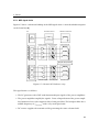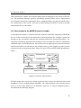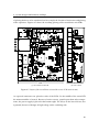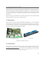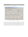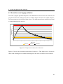
1
Master Thesis
Steffen Kaufmann
Design and Development of a Surveillance Unit
for a Safety-Critical Machine
Fakultät Technik und Informatik
Studiendepartment Informations- und
Elektrotechnik
Faculty of Engineering and Computer Science
Department Information and
Electrical Engineering
Steffen Kaufmann
Design and Development of a Surveillance Unit for a
Safety-Critical Machine
Master thesis based on the examination and study regulations for the
Master of Engineering degree programme
Information Engineering
at the Department of Information and Electrical Engineering
of the Faculty of Engineering and Computer Science
of the University of Applied Sciences Hamburg
Supervising examiner: Prof. Dr. rer. nat. Wolfgang Renz
Second examiner: Prof. Dr.-Ing. Karl-Ragmar Riemschneider
Day of delivery January 20th 2009
Steffen Kaufmann
Title of the Master Thesis
Design and Development of a Surveillance Unit for a Safety-Critical Machine
Keywords
Data logger, alarm system, surveillance unit, autonomic computing, FMEA, FTA,
embedded system, Magnetic Particle Imaging
Abstract
Surveillance is monitoring of behavior, activities, or other changing information.
Nowadays machines in the area of development and research as well as in a production environment getting more and more complex and expensive. Failures caused
by improper use or by defect parts can cause a lot of damage. To prevent or at least
to attenuate effects of such failures a surveillance unit is needed.
This master thesis analyzes requirements for surveillance units for safety critical machines. To demonstrate the concept the general approach will be specialized for the
surveillance of an MPI system. To support the design phase, the system is analyzed
with respect to Fault Tree Analysis (FTA) and Failure Mode and Effects Analysis
(FMEA).
Steffen Kaufmann
Thema der Masterarbeit
Design und Entwicklung von Hard- und Software einer Überwachungseinheit für
eine sicherheitskritische Maschine
Stichworte
Data-Logger, Alarm-System, Überwachungssystem, autonomic computing, FMEA,
FTA, embedded system, Magnetic Particle Imaging
Kurzzusammenfassung
Surveillance bezeichnet die Überwachung von Verhalten, Aktivitäten und anderen
veränderlichen Informationen. Maschinen in Forschung, Entwicklung und Produktion werden teurer und komplexer. Ausfälle, bedingt durch Fehlbenutzung oder defekte Teile, können beträchtliche Schäden verursachen. Um die Auswirkungen zu
verhindern oder zumindest abzumindern, wird eine Überwachungseinheit benötigt.
Diese Masterarbeit befasst sich mit Anforderungen an solch eine Überwachungseinheit. Die Anforderungen werden während des Designs und der Entwicklung
für eine sicherheitskritische Maschine weiter entwickelt und für die Anwendung in
einem MPI-System spezialisiert. Das System wird dafür mit Failure Mode and Effects Analysis (FMEA) in kombination mit Fault Tree Analysis (FTA) analysiert und
bewertet.
Acknowledgment
I wish to express my appreciation to T.M. Buzug, S. Biederer and the rest of the MPI-Team
at the University of Lübeck for the opportunity they have provided, the guidance and
the motivation. There courtesy, professionalism and patience made working with them
very rewarding and gratifying. Throughout the entire thesis work, they provided me with
timely and invaluable suggestions.
Special thank goes also to W. Renz and K.-R. Riemschneider for there supervision and
guidance of this thesis.
I would also like to thank M. Garz, M. Fricke and C. Rohde, for the chance they gave me
and S. Schrader for the knowledge he shared with me. During my work in the Garz &
Fricke company I learned at a lot useful skills and abilities and could deepen my engineering knowledge.
I am also very thankful for the help and assistance of my friends Andre, Kaja and Stephan
who have spent a lot of time to support the completion of this thesis.
At least I like to thank my parents for their constant support, inspiration and affectionate
assistance during my whole way.
Hamburg, January 2010
Steffen Kaufmann
IV
Contents
Contents
List of Figures
VIII
List of Acronyms
IX
1. Introduction
1.1. The current state . . . . . . . . . . . . . . . . . . . . . . . . . . . . . . . . . . .
1.2. The aim . . . . . . . . . . . . . . . . . . . . . . . . . . . . . . . . . . . . . . . .
1.3. Practical outline . . . . . . . . . . . . . . . . . . . . . . . . . . . . . . . . . . .
2. Basics
2.1. Data loggers, alarm devices and surveillance units . .
2.2. Risk analysis and FMEA . . . . . . . . . . . . . . . . .
2.3. Autonomic Computing and the MAPE-K control loop
2.4. Hardware basics . . . . . . . . . . . . . . . . . . . . . .
2.4.1. Embedded Systems . . . . . . . . . . . . . . . .
2.4.2. Microcontroller . . . . . . . . . . . . . . . . . .
2.4.3. Interfaces . . . . . . . . . . . . . . . . . . . . .
2.4.4. Data acquisition and processing . . . . . . . .
2.5. Magnetic particle imaging . . . . . . . . . . . . . . . .
2.5.1. MPI signal chain . . . . . . . . . . . . . . . . .
2.5.2. Single-sided scanner . . . . . . . . . . . . . . .
2.5.3. Magnetic Particle Spectrometer . . . . . . . . .
2.5.4. Cooling circuit . . . . . . . . . . . . . . . . . .
2.5.5. Summary . . . . . . . . . . . . . . . . . . . . .
2.6. Medical engineering standards . . . . . . . . . . . . .
2.7. Project roles and responsibilities . . . . . . . . . . . .
3. Technical analysis
3.1. Basic requirement analysis . . . . . . . . . . .
3.2. User interface . . . . . . . . . . . . . . . . . .
3.2.1. Direct user interaction . . . . . . . . .
3.2.2. Indirect user interaction . . . . . . . .
3.3. The real MPI scanner . . . . . . . . . . . . . .
3.4. Measurement acquisition . . . . . . . . . . . .
3.5. Risk analysis . . . . . . . . . . . . . . . . . . .
3.5.1. Hardware . . . . . . . . . . . . . . . .
3.5.2. Software . . . . . . . . . . . . . . . . .
3.5.3. Reduction of the system risk level . .
3.6. Multifunction considerations . . . . . . . . .
3.7. Failure detection, handling and timing . . . .
3.8. Connections to the MAPE-K reference model
.
.
.
.
.
.
.
.
.
.
.
.
.
.
.
.
.
.
.
.
.
.
.
.
.
.
.
.
.
.
.
.
.
.
.
.
.
.
.
.
.
.
.
.
.
.
.
.
.
.
.
.
.
.
.
.
.
.
.
.
.
.
.
.
.
.
.
.
.
.
.
.
.
.
.
.
.
.
.
.
.
.
.
.
.
.
.
.
.
.
.
.
.
.
.
.
.
.
.
.
.
.
.
.
.
.
.
.
.
.
.
.
.
.
.
.
.
.
.
.
.
.
.
.
.
.
.
.
.
.
.
.
.
.
.
.
.
.
.
.
.
.
.
.
.
.
.
.
.
.
.
.
.
.
.
.
.
.
.
.
.
.
.
.
.
.
.
.
.
.
.
.
.
.
.
.
.
.
.
.
.
.
.
.
.
.
.
.
.
.
.
.
.
.
.
.
.
.
.
.
.
.
.
.
.
.
.
.
.
.
.
.
.
.
.
.
.
.
.
.
.
.
.
.
.
.
.
.
.
.
.
.
.
.
.
.
.
.
.
.
.
.
.
.
.
.
.
.
.
.
.
.
.
.
.
.
.
.
.
.
.
.
.
.
.
.
.
.
.
.
.
.
.
.
.
.
.
.
.
.
.
.
.
.
.
.
.
.
.
.
.
.
.
.
.
.
.
.
.
.
.
.
.
.
.
.
.
.
.
.
.
.
.
.
.
.
.
.
.
.
.
.
.
.
.
.
.
.
.
.
.
.
.
.
.
.
.
.
.
.
.
.
.
.
.
.
.
.
.
.
.
.
.
.
.
.
.
.
.
.
.
.
.
.
.
.
.
.
.
.
.
.
.
.
.
.
.
.
.
.
.
.
.
.
.
.
.
.
.
.
.
.
.
.
.
.
.
.
.
.
.
.
.
.
.
.
.
.
.
.
.
.
.
1
1
2
3
.
.
.
.
.
.
.
.
.
.
.
.
.
.
.
.
5
5
7
12
14
14
15
15
17
18
20
22
23
24
24
24
25
.
.
.
.
.
.
.
.
.
.
.
.
.
27
27
28
29
29
30
31
32
32
32
33
34
34
36
V
Contents
3.9. Use and test cases . . . . . . . . . . . . . . . . . . . . . . . . . . . . . . . . . .
4. System design and hardware buildup
4.1. Selection of basic system components . .
4.1.1. Logic selection . . . . . . . . . . .
4.1.2. Microcontroller . . . . . . . . . . .
4.1.3. Program and data memory . . . .
4.1.4. Display and user interface . . . . .
4.1.5. Reaction interface . . . . . . . . . .
4.1.6. Communication interfaces . . . . .
4.1.7. Real time clock . . . . . . . . . . .
4.1.8. Future interface . . . . . . . . . . .
4.1.9. Acquirement of measurement data
4.1.10. Possibilities of debugging . . . . .
4.2. Chip select decoding logic . . . . . . . . .
4.3. Block diagram . . . . . . . . . . . . . . . .
4.4. ESD protection and PCB layout . . . . . .
4.5. Manufacturing . . . . . . . . . . . . . . . .
4.6. Initial operation . . . . . . . . . . . . . . .
37
.
.
.
.
.
.
.
.
.
.
.
.
.
.
.
.
.
.
.
.
.
.
.
.
.
.
.
.
.
.
.
.
.
.
.
.
.
.
.
.
.
.
.
.
.
.
.
.
.
.
.
.
.
.
.
.
.
.
.
.
.
.
.
.
.
.
.
.
.
.
.
.
.
.
.
.
.
.
.
.
.
.
.
.
.
.
.
.
.
.
.
.
.
.
.
.
.
.
.
.
.
.
.
.
.
.
.
.
.
.
.
.
.
.
.
.
.
.
.
.
.
.
.
.
.
.
.
.
.
.
.
.
.
.
.
.
.
.
.
.
.
.
.
.
.
.
.
.
.
.
.
.
.
.
.
.
.
.
.
.
.
.
.
.
.
.
.
.
.
.
.
.
.
.
.
.
.
.
.
.
.
.
.
.
.
.
.
.
.
.
.
.
.
.
.
.
.
.
.
.
.
.
.
.
.
.
.
.
.
.
.
.
.
.
.
.
.
.
.
.
.
.
.
.
.
.
.
.
.
.
.
.
.
.
.
.
.
.
.
.
.
.
.
.
.
.
.
.
.
.
.
.
.
.
.
.
38
38
38
39
39
40
41
41
42
42
42
43
44
45
47
49
49
5. Software implementation
5.1. Firmware of the surveillance unit . . . . . . . . . .
5.1.1. Implementation and organization . . . . .
5.1.2. System power up . . . . . . . . . . . . . . .
5.1.3. Serial communication . . . . . . . . . . . .
5.1.4. Watchdog . . . . . . . . . . . . . . . . . . .
5.1.5. Surveillance functionality . . . . . . . . . .
5.1.6. Mini shell . . . . . . . . . . . . . . . . . . .
5.1.7. System logbook and measurement logging
5.1.8. System configuration and autostart . . . .
5.1.9. File system . . . . . . . . . . . . . . . . . . .
5.2. PC configuration tool . . . . . . . . . . . . . . . . .
5.3. The communication layers . . . . . . . . . . . . . .
5.3.1. Debug port protocol . . . . . . . . . . . . .
5.3.2. Surveillance unit communication protocol
5.3.3. DC source protocol . . . . . . . . . . . . . .
.
.
.
.
.
.
.
.
.
.
.
.
.
.
.
.
.
.
.
.
.
.
.
.
.
.
.
.
.
.
.
.
.
.
.
.
.
.
.
.
.
.
.
.
.
.
.
.
.
.
.
.
.
.
.
.
.
.
.
.
.
.
.
.
.
.
.
.
.
.
.
.
.
.
.
.
.
.
.
.
.
.
.
.
.
.
.
.
.
.
.
.
.
.
.
.
.
.
.
.
.
.
.
.
.
.
.
.
.
.
.
.
.
.
.
.
.
.
.
.
.
.
.
.
.
.
.
.
.
.
.
.
.
.
.
.
.
.
.
.
.
.
.
.
.
.
.
.
.
.
.
.
.
.
.
.
.
.
.
.
.
.
.
.
.
.
.
.
.
.
.
.
.
.
.
.
.
.
.
.
.
.
.
.
.
.
.
.
.
.
.
.
.
.
.
.
.
.
.
.
.
.
.
.
.
.
.
.
.
.
.
.
.
.
.
.
.
.
.
.
.
.
.
.
.
51
51
51
53
54
55
55
57
58
59
60
60
63
63
63
64
6. System integration and validation
6.1. Hardware validation . . . . . . . . . .
6.1.1. Power supply . . . . . . . . . .
6.1.2. JTAG interface and core system
6.1.3. Digital IO . . . . . . . . . . . .
6.1.4. IIC and Real time clock . . . .
.
.
.
.
.
.
.
.
.
.
.
.
.
.
.
.
.
.
.
.
.
.
.
.
.
.
.
.
.
.
.
.
.
.
.
.
.
.
.
.
.
.
.
.
.
.
.
.
.
.
.
.
.
.
.
.
.
.
.
.
.
.
.
.
.
.
.
.
.
.
.
.
.
.
.
65
65
65
66
67
67
.
.
.
.
.
.
.
.
.
.
.
.
.
.
.
.
.
.
.
.
.
.
.
.
.
.
.
.
.
.
.
.
.
.
.
.
.
.
.
.
.
.
.
.
.
.
.
.
.
.
.
.
.
.
.
.
.
.
.
.
.
.
.
.
.
.
.
.
.
.
.
.
.
.
.
.
.
.
.
.
.
.
.
.
.
.
.
.
.
.
.
.
.
.
.
.
.
.
.
VI
Contents
6.1.5. Sensor PCB, SPI, ADC and DAC . . . . . . . . . . . .
6.2. Surveillance and logging validation . . . . . . . . . . . . . .
6.2.1. Surveillance and logging performance . . . . . . . . .
6.2.2. Reaction timings and measurement jitter verification
6.2.3. Functional runtime tracing . . . . . . . . . . . . . . .
6.3. System integration . . . . . . . . . . . . . . . . . . . . . . . .
6.4. Results . . . . . . . . . . . . . . . . . . . . . . . . . . . . . . .
.
.
.
.
.
.
.
.
.
.
.
.
.
.
.
.
.
.
.
.
.
.
.
.
.
.
.
.
.
.
.
.
.
.
.
.
.
.
.
.
.
.
.
.
.
.
.
.
.
.
.
.
.
.
.
.
.
.
.
.
.
.
.
68
69
70
71
73
73
74
7. Summary and future work
75
Bibliography
XV
A. CD-Contend
XVI
VII
List of Figures
List of Figures
1.1.
2.1.
2.2.
2.3.
2.4.
2.5.
2.6.
2.7.
2.8.
2.9.
2.10.
2.11.
3.1.
3.2.
3.3.
4.1.
4.2.
4.3.
4.4.
4.5.
4.6.
4.7.
4.8.
5.1.
5.2.
5.3.
5.4.
5.5.
5.6.
6.1.
6.2.
6.3.
6.4.
6.5.
6.6.
6.7.
Working and damaged transmitting Coil . . . . . . . . . . . . . .
Technolgy diagram: data logger, alarm devices, surveillance unit
Principle surveillance unit integration . . . . . . . . . . . . . . . .
Fault Tree Analysis - Example . . . . . . . . . . . . . . . . . . . . .
MAPE-K reference model . . . . . . . . . . . . . . . . . . . . . . .
Magnetic field propagation in MPI . . . . . . . . . . . . . . . . . .
MPI particle response in magnetic fields . . . . . . . . . . . . . . .
Schematic MPI hardware setup . . . . . . . . . . . . . . . . . . . .
Schematic MPI scanner setup . . . . . . . . . . . . . . . . . . . . .
Schematic single-sided MPI setup . . . . . . . . . . . . . . . . . . .
Schematic single-sided MPI scanner setup . . . . . . . . . . . . . .
Principle MPS Setup . . . . . . . . . . . . . . . . . . . . . . . . . .
Picture: AC Power amplifier and DC power supply . . . . . . . .
Illustration of different limit violations . . . . . . . . . . . . . . . .
MAPE-K implementation . . . . . . . . . . . . . . . . . . . . . . .
Picture of a ATMega1280 microcontroller . . . . . . . . . . . . . .
Drawing of the user interface . . . . . . . . . . . . . . . . . . . . .
Simplified chip selection decoding logic . . . . . . . . . . . . . . .
System block diagram . . . . . . . . . . . . . . . . . . . . . . . . .
Principle ESD of routing . . . . . . . . . . . . . . . . . . . . . . . .
Principle of the PCB buildup . . . . . . . . . . . . . . . . . . . . .
Layout of the surveillance unit and the sensor PCB . . . . . . . . .
Picture of the surveillance unit PCB . . . . . . . . . . . . . . . . .
Buildup of the firmware software . . . . . . . . . . . . . . . . . . .
Principle function of a Round-Robin . . . . . . . . . . . . . . . . .
Flow diagram: Function Surveillance . . . . . . . . . . . . . . . . .
Flow diagram: Mini shell . . . . . . . . . . . . . . . . . . . . . . .
PC configuration tool: main window . . . . . . . . . . . . . . . . .
PC configuration tool: debug and command window . . . . . . .
System power consumption over the Input voltage range . . . . .
Picture of the Adapter PCBs . . . . . . . . . . . . . . . . . . . . . .
ADC/DAC verification . . . . . . . . . . . . . . . . . . . . . . . . .
Temperature measurement with limits . . . . . . . . . . . . . . . .
Zoomed temperature measurement . . . . . . . . . . . . . . . . . .
Jitter and Delay measurement buildup . . . . . . . . . . . . . . . .
Reaction timing measurement . . . . . . . . . . . . . . . . . . . . .
.
.
.
.
.
.
.
.
.
.
.
.
.
.
.
.
.
.
.
.
.
.
.
.
.
.
.
.
.
.
.
.
.
.
.
.
.
.
.
.
.
.
.
.
.
.
.
.
.
.
.
.
.
.
.
.
.
.
.
.
.
.
.
.
.
.
.
.
.
.
.
.
.
.
.
.
.
.
.
.
.
.
.
.
.
.
.
.
.
.
.
.
.
.
.
.
.
.
.
.
.
.
.
.
.
.
.
.
.
.
.
.
.
.
.
.
.
.
.
.
.
.
.
.
.
.
.
.
.
.
.
.
.
.
.
.
.
.
.
.
.
.
.
.
.
.
.
.
.
.
.
.
.
.
.
.
.
.
.
.
.
.
.
.
.
.
.
.
.
.
.
.
.
.
.
.
.
.
.
.
.
.
.
.
.
.
.
.
.
.
.
.
.
.
.
.
.
.
.
.
.
.
.
.
.
.
.
.
.
.
.
.
.
.
.
.
2
6
6
8
13
18
19
20
21
22
23
23
30
35
36
39
41
44
46
47
47
48
49
52
55
56
58
61
62
66
67
68
69
70
71
72
VIII
List of Acronyms
List of Acronyms
IIC Inter-Integrated Circuit
ISP In System Programming
ADC Analog Digital Converter
ALARP As Low As Reasonably Practicable
JTAG Joint Test Action Group
API Application Programming Interface
LED Light Emitting Diode
ASCII American Standard Code for Information
LNA Low Noise Amplifier
Interchange
BCD Binary Coded Decimal
MMC Multi Media Card
MPI Magnetic Particle Imaging
CPU Central Processing Unit
DAC Digital Analog Converter
DIO Digital Input/Output
DMM Digital Multimeter
MPS Magnetic Particle Spectrometer
PC Personal Computer
PCB Printed Circuit Board
POST Power-On Self-Test
DSP Digital Signal Processor
RISC Reduced Instruction Set Computing
EEPROM Electrical Erasable Programmable Read
RPN Risk Priority Number
Only Memory
RTC Real Time Clock
EMI Electromagnetic Interference
ESD Electrostatic Discharge
ETA Event Tree Analysis
SAR Specific Absorption Rate
SD Secure Digital
FAT File Allocation Table
SDHC Secure Digital High Capacity
FFP Field-Free Point
SPI Serial Peripheral Interface
FIFO First In First Out
SPIO Superparamagnetic Iron Oxide
FMEA Failure Mode and Effects Analysis
SUCP Surveillance Unit Communication Protocol
FPGA Field Programmable Gate Array
SVN Subversion
FTA Fault Tree Analysis
GCC GNU Compiler Collection
GPIO General Purpose Input/Output
GPL GNU Public License
GUI Graphical User Interface
IC Integrated Circuit
TAP Test Access Point
TCK Test Clock
TDI Test Data In
TDO Test Data Out
TMS Test Mode Select
TRE Total Risk Estimate
IX
List of Acronyms
TRST Test Reset
TWI Two Wire Interface
UART Universal Asynchronous Receiver/Transmitter
USB Universal Serial Bus
VIA Vertical Interconnect Access
X
1. Introduction
Surveillance is monitoring of behavior, activities, or other changing information. The word
surveillance comes from the French word for ´´watching over”. Nowadays machines in the
area of research and development as well as in a production environment getting more and
more complex and expensive. Failures caused of improper use or failures caused of defect
parts can cause a lot of damage. To prevent or at least to attenuate the effects of such
failures surveillance and reaction is the only solution. An advantage of preventing failures
is reduction of machine damage and repair fees in a failure case. This leads to, in most
cases the more interesting part, the reducing of the system down time.
A human being is normally not able to handle such failures, caused of one main reason the
lack of permanent vigilance. This means a human being is not able react in a time frame
which prevents further damage, ether if only small system parameters have to change.
To overcome this problematic a machine is needed, which can detect failures and handles
failure-situations. Such a machine is called surveillance unit.
1.1. The current state
In 2005, Gleich and Weizenecker presented a new tomographic imaging technique called
Magnetic Particle Imaging (MPI) [18]. Based on the non-linear magnetization of magnetic
nanoparticles, the spatial distribution of these nanoparticles can be determined.
In the University of Lübeck an MPI scanner system runs so far without a surveillance unit.
This lead in the past to smaller accidents. Figure 1.1 shows for example a burned coil, cause
of the forgotten switch on of a cooling fan.
1
1. Introduction
(a) New transmitting coil
(b) Burned transmitting coil
Figure 1.1: Working and damaged transmitting Coil
Other possible failure cases are for example high voltages at outputs of power amplifiers,
caused by wrong input voltages or a malfunction of power amplifiers. It is obvious that
this status is unhealthy. The danger for the machine, patients and the people, which are
working with it, is not arguable.
Cause of the fact, MPI scanners are also in the developing process, a monitoring of the
system parameters such as scanner temperatures or changing of currents and voltages over
time are quite interesting. At the moment the only possibility to measure such effects is to
do it manually with a bunch of Digital Multimeter (DMM)s.
To overcome the sketched problematic a surveillance unit is needed, which handles intermittent failures.
1.2. The aim
The aim of this work is the analysis of common system-failure cases for safety-critical machines and the design of a surveillance unit for those machines. To verify the design a
surveillance unit for MPI systems will be developed and designed. The developed surveil-
2
1. Introduction
lance unit should assure a save system operation and an adequate handling of failure cases.
This should be done by monitoring parameters and reacting to failure cases. Another aspect which is quite interesting is the possible detection of wastage in the system to provide
a just in time maintenance. To detect failures and system changes the surveillance unit
should also record measurements for subsequently analysis and evaluation.
In this master thesis the requirements are logically split up in two parts. A more general
generic part and a more specialized part. The generic part provides a bunch of requirements which are valid for all types of safety-critical machines. The specific part provides a
case study for an MPI scanner system1 surveillance unit. This approach makes the results
of this master thesis suitable for application domains beyond MPI.
1.3. Practical outline
The practical work of this master thesis consists of the development and design of a surveillance unit with respect to the outlined requirements and the testing of these criteria. The
following work-flow is planned:
• Technical analysis and refining of defined requirements
In this part the requirements are refined with the expertise from the technical analysis. The system buildup is designed and communication protocols are developed.
• Development and design of the hardware and the Printed Circuit Board (PCB)
Within the development and design the hardware components will be selected, the
schematics will be drawn and the PCB layout will be done.
• Development and design of the surveillance firmware
In this phase the hardware of the surveillance unit will be programmed, it is also the
first hardware commissioning and therefore the first hardware test. This fact makes
the phase complicated, because software malfunctions can also be hardware-issues.
• Development and design of the configuration tool
In this phase the development and design of the PC configuration program and a
refining of the communication protocols is done.
1 The
functionality of an MPI system will be described in chapter 2.5 on page 18.
3
1. Introduction
• Integration of the surveillance unit into the MPI scanner system
In this phase the developed design will be integrated into the MPI system. A ebbing
to previous steps for smaller changes is likely.
• Test and validation of the components
In the test and validation phase a system test will be performed to ensure a proper
operation of the current MPI system with the integrated surveillance unit.
• Review and redesign
In this phase the solution will be reviewed and a redesign will be planed, with the
expertise of the test and validation phase.
Additionally to the theoretic development and design, this master thesis contains a description of the practical work and the decisions made are explained.
4
2. Basics
In this chapter related technologies and methods are discusses. The expertise of this chapter is needed for further parts of this work.
2.1. Data loggers, alarm devices and surveillance units
So called data loggers, alarm devices and surveillance units are available at individual
markets. The names are closely related, so also the usage of them. Data loggers are devices
which record measurements over time. The recording medium is in most cases a simple
flash memory, Multi Media Card (MMC) / Secure Digital (SD) or Compact Flash card. On
the market are many data logger available, but most of them have no possibility to configure measurement limits to produce an alarm. Most devices support additional communication interfaces like RS232, USB or Ethernet. Supported analog or digital channel-count
is up 32 with a resolution range from 8 bit to 24 bit at sample frequencies of about 0.1 Hz to
100 Hz.
Most data loggers are specific to their application and support only a small amount of input
signals like pressure, humidity or temperature. Data loggers that are produce an alarm, if
configured limits are overridden are called alarm devices. Alarm devices are often limited
in ether there configuration possibilities or their channel counts.
A surveillance unit, in context of this thesis, is a device which is able to acquire, process
and store data. The processing can detect limit crossings and can trigger appropriate reactions. Available surveillance units are much more specialized than data loggers or alarm
devices. The application area is limited, which allows a good matching to demands and
functionality of the monitored machine. For example in many critical systems the securing
is done redundant. This could for example mean two switches in series in a simple case, or
a system with two parallel Integrated Circuit (IC), if keeping of fast real time requirements
is needed. Figure 2.1 show the conntection between surveillance units, alarm devices and
data loggers.
5
2. Basics
Surveillance Unit
Data logger
Alarm device
A
A
D
D
Acquire and store data
Acquire and monitor limits, can produce alarms
Combination of data logger and alarm device, extend the requirements and provides greater flexibility
Figure 2.1: Technolgy diagram: data logger, alarm devices, surveillance unit
Another approach of system organization is decentralization handling. Decentralization
handling means that errors are handled where they occur. A surveillance unit in such a
system has only to communicate with subsystems. This means for example that moving
parts have cam switches, which are shutdown the power source of the electric engine in
a failure case. This approach has the advantage of minimizing the involved fault-prone
hardware.
All disclosed facts, make the porting of a surveillance units or even the concept complicated. Therefore in most cases a complete redesign of the safety concept and surveillance
unit is needed. Figure 2.2 shows a principle integration of a surveillance unit into a system.
Surveillance unit
Sensor Interface
User Interface
Logic
System
Storage
Reaction Interface
Figure 2.2: Principle surveillance unit integration
The surveillance unit is connected through sensors to the system, configured limits allow
an evaluating of the system status. The reaction interface allows an interaction between
6
2. Basics
surveillance unit and system. The interaction could for example be enabling, configuration
or shutdown of system parts. A user interface allows monitoring the surveillance unit or
change surveillance parameters.
2.2. Risk analysis and FMEA
[1] describes risk analysis as ”Part of the project analyzes, which focus on project risks”.
Aims of risk analysis are multifaceted but the main goals are according to [30]:
• Improvement of reliability
• Reducing of warranty and accommodation costs
• Adherence to delivery dates, cause of avoiding errors in research, development and
production
Project risks for new machines are complex, adjacent economic and environment risks, the
technical risks of the projected machine itself is critical2 . Risk analysis can be done with
a lot of different risk analyzing techniques. All techniques have in common that they are
systematic approaches. One possible approach is Fault Tree Analysis (FTA) [2] [3]. The FTA
focus on the possible risks, called hazards, by reducing hazards to single sub-hazards, and
these sub hazards to further sub-sub-hazards this approach forms a tree, the so called fault
tree. A bottom-up approach is use of Event Tree Analysis (ETA) [27]. In ETA, in difference
to FTAs, in which hazards are the root event, the failures are investigated. Figure 2.3 shows
an example for FTA.
2 This
thesis focus on the projected machine itself, not on the whole project.
7
2. Basics
Figure 2.3: Fault Tree Analysis - Example [25]
An approach to investigate, besides error severity and occurrence the probability is Failure
Mode and Effects Analysis (FMEA) [27] [14]. FMEA yields in the so called Risk Priority
Number (RPN). The RPN is determined from severity, occurrence and the detection rate.
FMEA, first used in 1960’s in the Aerospace industry, is used widely in the manufacturing
industries in various phases of the product life cycle.
Failure modes in FMEA are any errors or defects in a process, design or item, especially
those that affect the customer. Failure modes can be potential or actual. Effects analysis
refers to studying the consequences of those failures.
Table 1 shows the classification of occurrence probability and severity of hazards in FMEA:
Probability
Occurrence
Severity
Description
frequent
in nearly every use
critical
possibility of death, heavy injury
feasible
occurs regularly, especially induced
or damage
by other failures
marginal
possibility of injury or damage
occasional
occurs sometimes
negligible minimal or no possibility of in-
conceivable
occurs seldom, in extreme examples
unlikely
never occurred so far, will probably
jury or damage
never occur
systematic
no probability can be determined:
errors
software of user failure (cf. IEC 601)
Table 1: FMEA Occurrence Probability and Severity of Hazards Classification [27]
8
2. Basics
In risk analysis of technical systems it is often not possible to determine absolute numbers
for incidence of an error. Therefore table 1 shows only categories for error occurrence
probability as well as for the severity of an error.
Independent of applied techniques such as FTA, ETA or FMEA, risk management is applied as an iterative process, which is organized in following steps:
1. Detection of risks (hazards)
2. Devising of actions for risk control
3. Implementing of risk minimization, if possible
4. Verifying of the residual risk and deciding: Is the risk acceptable?
5. Detection of new hazards are generated
6. Restarting the procedure with step 1
It is well known that this process has to be continued until hazards are confirm with “As
Low As Reasonably Practicable (ALARP)-Principle”. This risk minimization can be performed by following three methods:
1. System design
2. Implementation of protection mechanisms
3. Implementation of warnings
These methods should be applied in the given order. This means that only, if no reasonable
design or protection mechanism can be found (in view of cost and effort), it is admissible
to give “just” warnings. These warnings are given in the user’s manual or of labels directly
attached to the system.
It is important to apply dedicated methods for designing and prototyping safety-critical
machines. Further systematic methods for risk analysis and management need to be applied in order to assure the proclaimed safety. Such methods help to improve the system
and are prerequisites for further certifications [27].
Cause of the fact, that development of software is also a fault-prone process, FMEA can
also be used for the software development process [11]. Conventional test cases only test
9
2. Basics
behavior on predicted inputs. Predicted inputs can be permitted or wrong inputs that are
selected by tester. Cause of test complexity it is not possible to test any case. FMEA can
also be used to analyze the effects of such failures with respect to system behavior. FMEA
provides a theoretical method to analyze every error source of a component [11].
In this Master Thesis FMEA is used for analyzing the failure behavior of the surveillance
unit itself, the MPI -System in general and the software. Tasks which have to be answered
are:
• Which failures can occur within the system?
• Which effects have such failures?
• Which actions take place to avoid such failures?
• Which actions take place to handle unavoidable failures?
• How big is the residual risk?
• Which are unavoidable failures?
As mentioned before to bring the severity, occurrence and detectability together the RPN
is used. Equation 1 shows the calculation of the RPN. S is the severity, O the occurrence
and D the detectability. The Values are in the Range of 1 to 10, whereby 1 is the best case
and 10 the worst case.
RPN = S · O · D
(1)
Equation 2 shows the calculation of the Total Risk Estimate (TRE) which is calculated from
the RPN [14].
n
TRE =
100%
∑ RPNi · n · 1000
(2)
i =1
The TRE is characterizing the overall risk level for a given project, where RPNi are RPN
values for a given i-th cause and n is the number of causes in the FMEA table. Cause the
RPN values, for three RPN components ranked on a 1 to 10 scale, are fluctuating between
1 and 1000, it is obvious that the TRE values will always are between 0.1 % and 100 %.
10
2. Basics
A boundary value of approximately 17 % corresponds to the multiplied Midpoint (5.5),
therefore the Risk acceptability criteria could be established as 17 % [14].
This does not mean that no corrective action is required for TRE < 17%. Obviously, extremely high RPN values should be dealt with. Nevertheless, calculated TRE values could
be used for comparative analysis of different processes or operations in order to focus efforts on the most critical operation, or as an indicator of design maturity when deciding to
claim a design freeze and transfer a design to production [14]3 .
3 The
out comings of FMEA can be found in chapter 3 - Technical Analysis on page 27; the tables itself in
located the appendix
11
2. Basics
2.3. Autonomic Computing and the MAPE-K control loop
For developing a high quality surveillance unit, a portion of autonomy is needed. Inspired
by biology, autonomic computing is a concept that brings together many fields of computing with the purpose of creating computing systems that self-manage. Computing systems
have reached a level of complexity where human effort required to get the systems up and
running and keeping them operational is getting out of hand. The main properties of selfmanagement as portrayed by IBM are self-configuration, self-optimization, self-healing
and self-protection [22] [23].
• Self-configuration
An autonomic computing system configures itself according to high-level goals. A
system operate without the direct intervention of users and have some kind of control
over their actions and internal state. To achieve this the system can interact with other
systems and users.
• Self-optimization
An autonomic computing system optimizes its use of resources. It may decide to
initiate a change to the system proactively (as opposed to reactive behavior) in an
attempt to improve performance or quality of service. The system perceive its environment and respond in a timely fashion to changes that occur in it.
• Self-healing
An autonomic computing system detects and diagnoses problems. If possible, it
should attempt to fix the problem, for example by switching to a redundant component (see for example [24]). However, it is important that as a result of the healing
process the system is not further harmed, for example by the introduction of new
bugs or the loss of vital system settings. Fault-tolerance is an important aspect of
self-healing. For a given stimuli, the system´s ability to adapt correctly and maintain
expected behavior sets contributes to the degree of trust to its sensors.
• Self-protection
An autonomic system protects itself from malicious attacks but also from end users
who inadvertently make system changes. The system autonomously tunes itself
12
2. Basics
to achieve security and data protection. Security is an important aspect of selfprotection, not just in software, but also in hardware.
The autonomic community is identifying a system as autonomic if it exhibits more than one
of the self-management properties. An ultimate goal of autonomic computing is to automate management aspects of complex distributed systems. To achieve autonomic computing, IBM has suggested a reference model for autonomic control loops, which is sometimes
called the MAPE-K (Monitor, Analyse, Plan, Execute, Knowledge) loop. Figure 2.4 shows
IBM´s MAPE-K reference model for autonomic control loops.
Figure 2.4: IBM‘s MAPE-K (Monitor, Analyze, Plan, Execute, Knowledge) reference model for
autonomic control loops [22].
In the MAPE-K autonomic loop, the managed element represents any software or hardware resource that is given autonomic behavior by coupling it with an autonomic manager. The managed element can for example be a specific part or software component or
a complete system. The data collected by the sensors allows the autonomic manager to
monitor the managed element and execute changes through effectors.
The autonomic manager is a software component that ideally can be configured by human administrators using high-level goals and uses the monitored data from sensors and
internal knowledge of the system to plan and execute, based on these high-level goals,
the low-level actions that are necessary to achieve these goals. The types of monitored
13
2. Basics
properties, and the sensors used, will often be application-specific, just as effectors used
to execute changes to the Managed Element are also application-specific. For the monitoring of a system two types of monitoring can be identified passive and active. Passive
monitoring of a system can be easily done by using existing monitor functionality. Active
monitoring needs engineering at some level for example modifying and adding source
code or populating sensors.
To characterize the level of autonomy IBM have proposed adoption model levels that spans
from level 1: Basic, to level 5: Autonomic. Briefly, level 1 defines the state whereby system
elements are managed by highly skilled staff who utilize monitoring tools and then make
the require changes manually. Level 2 is known as managed. This is where the system´s
monitoring tools collage information in an intelligent enough way to reduce the systems
administration burden. Level 3 is entitled predictive whereby more intelligent monitoring than level 2 is carried out to recognize system behavior patterns and suggest actions
approved and carried out by IT staff. The adaptive level is level 4. Here the system uses
the types of tools available to level 3 system´s staff but is more able to take action. Human interaction is minimized and it is expected that the performance is tweaked to meet
service level agreements. Finally, the full autonomic level is level 5, where systems and
components are dynamically managed by business rules and policies, thus freeing up staff
to focus on maintaining at a higher level. Another higher step is when the system is able
to use its intelligence to drive the self management to grow and refine itself to work in a
closed-loop. [22] [23]
2.4. Hardware basics
To understand the hardware development process, basic knowledge is necessary. The following subsections will describe the key components of an embedded system.
2.4.1. Embedded Systems
Embedded systems are embedded computer systems designed to perform one or a few
dedicated functions often with real-time constraints. In contrast Personal Computer (PC)
are designed to be flexible and to meet a wide range of an end-user’s needs.
14
2. Basics
Since embedded systems are dedicated to specific tasks, the design is optimized to the
product demands which also improve the reliability and performance [20].
2.4.2. Microcontroller
Microcontrollers are the central point in embedded systems and in most cases starting
point of the component selection. Microcontrollers consist minimal of a Central Processing
Unit (CPU), Memory and General Purpose Input/Output (GPIO)s. Most microcontrollers
also employ interfaces like Universal Asynchronous Receiver/Transmitter (UART), Serial
Peripheral Interface (SPI), Inter-Integrated Circuit (IIC) or Universal Serial Bus (USB).
For a reliable solution a proved microcontroller has to be chosen. An approved starting
point is Atmel AVR family. These microcontrollers provide a lot of interfaces and have
also a lot of memory. Another important point is, that a free available open source compiler
from the GNU Compiler Collection (GCC) is available [42] [10].
2.4.3. Interfaces
To enable a communication between different devices appropriate communication interfaces are needed. In this section common interfaces are described briefly.
• Serial character interfaces (USB-)UART
A UART is a bidirectional asynchronous serial communication interface. Nowadays
most new PCs, in comparison to microcontroller, do not have UARTs externally available. The USB interface has displaced UART interfaces in PCs. Cause of this fact a
USB to UART interface is needed. These interfaces provide a low level UART interface to the microcontroller and a USB interface to the PC. Needed drivers for the
USB device are supplied by the chip manufacturer. On the PC side the microcontroller connected to UART looks like a serial port, which enables an uncomplicated
programming on the PC side.
UARTs are generally used for basic debugging and communication on embedded
systems. The uncomplicated handling of UARTs allows testing and debugging in
early development phases.
15
2. Basics
• Chip level interfaces: SPI, IIC and OneWire
In digital circuits the number of signals is critical with respect to layer count, space
and costs. Reduction of signals means in the most cases reducing of Printed Circuit
Board (PCB) space, PCB layer count and costs. To serve such demands a lot of chip
level interfaces are available on the market. Well known examples are SPI, IIC and
OneWire. OneWire is a one signal interface. The signal line is a bidirectional communication and a power line. The addressing of different slaves is done with hardwired
slave addresses. Cause of the fact that OneWire has only one signal line, OneWire has
a disadvantage of slow communication speed, about 16,3 KBit/s. Common OneWire
devices are small sensors and Real Time Clock (RTC).
A faster communication can be achieved by using IIC buses4 . IIC consists of the
signals clock and data. The data signal is bidirectional and the addressing of IIC
devices is done by hardwired slave addresses. IIC enables communication speeds
up to 400 KBit/s. Common IIC devices are RTC, multiplexer, amplifier or Electrical
Erasable Programmable Read Only Memory (EEPROM).
One fast common technique of transmitting data on chip level is SPI. SPI consists of
four signals: clock, chip select, data-out and data-in. Cause of dedicated data signals
SPI has the possibility of a full duplex mode. SPI devices are available with speeds
up to about 16 MBit/s. A drawback, which is also an advantage, of SPI is need of chip
selection. Chip selection can be quite complex, if more devices are connected to the
SPI bus. Common SPI devices are Analog Digital Converter (ADC), Digital Analog
Converter (DAC) and different kinds of memories.
• Debugging and programming interfaces: JTAG and ISP
In contrast to desktop programming, in embedded systems is in most cases no operating system available. To provide access to the program memory two interfaces are
common: Joint Test Action Group (JTAG) and In System Programming (ISP).
A JTAG interface is one of the low level interfaces and also one of the most important
ones on hardware devices. JTAG enables real time debugging as well as programming and verification.
4 IIC
is also known as Two Wire Interface (TWI)
16
2. Basics
JTAG consists normally of five signals Test Data In (TDI), Test Data Out (TDO), Test
Mode Select (TMS), Test Clock (TCK), Test Reset (TRST). These signals are called
Test Access Point (TAP). With them various tests and programming tasks are possible. The speed of operation depends on chip itself but is typically in a range of
10-100 MBit/s.
In contrast to JTAG, an ISP interface is less complex. ISP provides only a possibility to
program a device. In most cases ISP is an extended SPI interface, which is modified
to the needs of the microcontroller.
2.4.4. Data acquisition and processing
The acquisition of data in microcontroller systems can be done basically in two ways: digital and analog. Digital can mean a chip level interface or only high and low. Analog inputs
are more common in case of acquisition of measurement data. An alternative is the use of
smart sensor networks. With smart sensors arranged in a network it is possible to achieve
fault tolerance [24].
The handling of digital input signals can in most cases be done by the microcontroller itself,
in difference the handling of analog input signals is more complex. The input range must
be fit, sample rate and accuracy must be high enough. Normally microcontrollers itself
have a small amount of Analog Digital Converter (ADC) channels, but in most cases the
acquisition time is high and the accuracy pure. An alternative is to use external ADC. Fast
accurate external ADC are available for example for SPI or IIC.
The processing of the measured data can be done within the microcontroller, if no complex operation on the data is needed or within an Digital Signal Processor (DSP), Field
Programmable Gate Array (FPGA) or after logging and storing afterward within the PC, if
complex operations are necessary.
17
2. Basics
2.5. Magnetic particle imaging
MPI is a new imaging method which was introduced in 2005 [18]. The idea of MPI is to exploit the nonlinear magnetization curve of Superparamagnetic Iron Oxide (SPIO) nanoparticles for imaging their spatial distribution.
A called ´´selection field”, which is relatively high at the edges but approaches zero in the
center is applied to these nanoparticles. This central point is referred to as Field-Free Point
(FFP). The SPIO outside the FFP, i.e. located in high field, will be saturated and therefore
unaffected by any applied field, while SPIO within the closely defined FFP will be free
to respond. Figure 2.5 shows the basic field propagation between the selection field coils,
which are buildup as Maxwell-Coils5 .
Figure 2.5: Magnetic field propagation in MPI [36]
The resolution in MPI is determined solely by size of area of non-saturated nanoparticles
around the FFP, independently of size of detectors, providing a resolution of 1 mm or
less [17] [18].
5A
Maxwell coils describes a buildup of two coils which are parallel to each other, the current direction is
opposite to each other.
18
2. Basics
If a sinusoidal oscillating magnetic field, called ´´drive field” is applied to the SPIO in the
FFP, the SPIO will “respond” with oscillations at same frequency as applied magnetic field.
Cause of magnetic saturation of the nanoparticles these M field has nearly a rectangular
shape. This means in frequency domain the induced signal has additional to the base frequency an add on of a series of higher harmonics. These harmonics can be separated from
the applied signal by appropriate filtering, providing a signal that can be unambiguously
assigned to the narrow FFP [12]. Figure 2.6 shows the basic MPI principle.
(a) Particle response on oscillating magnetic field.
(b) Particle response on oscillating magnetic field
The SPIO are free to respond. [37]
with offset. The SPIO are saturated, therefore
nearly no signal is responded. [37]
Figure 2.6: MPI particle response in magnetic fields
For a spatial imaging a movement of the FFP is needed. This is achieved by superimposing
a sinusoidal signal with slightly different frequencies to the different selection fields. The
resulting trajectory of the FFP looks like a Lissajous figure [26].
To archive a proper result, without harming patients cause of heating MPI use field strengths
of about 20 mT/µ0 [18]. The Specific Absorption Rate (SAR) tolerance value is an estimate
based on a drive field frequency up to 100 kHz [15].
19
2. Basics
2.5.1. MPI signal chain
Figure 2.7 shows a schematic buildup of the MPI signal chain. A more detailed description
can be found in [40].
PC
DC Power Source
Transmit Signal Generation
DC
Source
Control
Selection Field Coils
DC
Source
Power Amplifier Band Pass Filter
Drive Field Coils
fX
fY
fZ
Receive Signal Analysis
Magnetic Nanoparticles
fX
fY
fZ
Low Noise Amplifier Band Stop Filter
Receive Coils
Figure 2.7: Schematic MPI hardware setup
The signal chain is as follows:
• The PC generates with a DSP card determined input signals of the power amplifiers.
• The power amplifiers amplify the signals. Cause of imperfection of the power amplifier, harmonics have to be suppressed by a band pass filter. The bandpass filter has a
middle frequency of f Transmitter with a very small pass band.
• DC sources supplies the transmit coil for generating the static selection field.
20
2. Basics
• Power amplifiers providing the superimposed drive field.
• Transmit coils and the receiving coils acting in connection with the SPIO like non
linear transformers, and adding the non linear harmonics
• On secondary side of transformer the original transmitting frequencies ( f x , f y and
f z ) will be attenuated with a notch filter to allow a amplification of weak harmonics
without clipping the low noise amplifier caused by strong base frequencies.
• The output of the Low Noise Amplifier (LNA) will be digitalized and further computed.
A problem within designing of MPI Low Noise Amplifier (LNA) is bandwidth, distributed
over two decades, in connection with very small signal amplitude. This makes the designing of a suitable receiving amplifier complicated [40].
This design describes the common MPI scanner buildup as a cave. The advantage is
straight forward design, disadvantage is the needed size to image a human being. Figure 2.8 shows the principle buildup with a 2D-Design.
Figure 2.8: Schematic MPI scanner setup [36]
The green and red coils are transmitting coils (combined drive field and selection field
coils), the blue coils are receiving coils. The black area in the middle sketches the field of
view.
21
2. Basics
2.5.2. Single-sided scanner
Another possible buildup of a MPI scanner is a single-sided approach. This buildup enables smaller imaging devices, which are for example usable like ultrasonic devices. Figure 2.9 shows the principle hardware buildup. The main difference to the conventional
buildup (see figure 2.7) is lack of a needed cave. In the signal path a additional DC
source, a combined transmit coils and cause of the interconnection of the DC source and
the AC power amplifier also an AC blocker to protect the DC source from the AC signal, is
needed [35].
DC Power Sources AC-Blocker
PC
Transmit Signal Generation
DC
Source
Control
DC
Source
DC
Source
Power Amplifier
Transmit Coils
Band Pass Filter
fX
fY
fZ
Receive Signal Analysis
Magnetic Nanoparticles
fX
fY
fZ
Low Noise Amplifier Band Stop Filter
Receive Coils
Figure 2.9: Schematic single-sided MPI setup
Figure 2.10 shows a schematic single-sided MPI scanner setup [38]. The single-sided MPI
scanner setup is buildup to be more portable and handy as the cave design. All coils are
organized in a small case.
22
2. Basics
Figure 2.10: Schematic single-sided MPI scanner setup [36]
2.5.3. Magnetic Particle Spectrometer
The third setup is the Magnetic Particle Spectrometer (MPS). The MPS is used to characterize properties of nanoparticles itself. The MPS is a simplified buildup of the conventional
design [13].
Figure 2.11: Principle MPS Setup: The outer green coil is the transmitting coil, the blue coil is the
receiving coil and in the center is the probe chamber [13].
Figure 2.11 shows principle of a MPS setup. The outer green coil is the transmitting coil,
the blue coil is the receiving coil and in the center is the probe chamber. Cause of simple
buildup all system parameters could be measured or calculated. With this knowledge it is
23
2. Basics
possible to characterize properties of nanoparticles in the probe chamber. The signal path
is a subset of the signal path of the conventional scanner.
2.5.4. Cooling circuit
Cause of needed field strengths high coil current is needed for drive and selection field.
Cause of the resistance of the coil-wire high power dissipation occurs. The dissipated
power must be conducted through a cooling circuit. Possible cooling circuits are filled
with air, oil or water depending on the need of cooling performance. Measures are for
example temperature, pressure or flow of cooling fluids.
2.5.5. Summary
In various papers, imaging performance of MPI was proven [44] [19] [38], but safety aspects of an MPI system were neglected in past. Thereby MPI systems contain different
risks for example the overheating of transmitting coils, voltage breakdowns, or exceeding
of maximum magnetic field strengths. All these examples imply a potential risk to damage
hardware and harm users or patients in medical applications.
2.6. Medical engineering standards
Medical devices generally have to fulfill high safety standards to ensure reliable function,
expected health protection and patient’s benefit. This demands a functional and structured
quality management from beginning of development and engineering process. At beginning of the 90th the requirements for medical devices have been harmonized in the EU.
The lawmakers implemented usage of quality management6 as requirement in medical
products. Personal responsibility and self control have gained a higher meaning and are
indispensable for a successful marketing approval [41].
According to [4] surveillance units (including software) for MPI scanner are part of MPI
systems and have to fulfill specified guidelines7 . [4] also groups medical devices by their
6 Guideline
93/42 EWG recommends a quality management according to ISO 9000 in connection with
EN 46000.
7 The used tracer is not part of the system and is an independent issue
24
2. Basics
application, therefore an MPI system is likely a class 1 product and has to fulfill following
project demands:
• security measures, risk minimization and warnings for remaining risk
• effectivity certification
• repeatability of results
• adherence of certification tokens
For all devices placed on the European market a CE characterization is needed. To obtain a
CE certification basic requirements of quality, capability (medicine and technique), safety
and innocuousness of health (for patients and users) have to be kept. For medical devices an additional independent conformity assessment procedure has conducted also [9].
Needed CE-documentation has to include at least a product description, classification and
used conformity assessment procedure, engineering documentation, clinical evaluation,
risk analysis and a user manual [31] [39].
The surveillance unit described in this Master Thesis is used at the Institute of Medical
Engineering at the University of Lübeck as a research-technology demonstrator but not yet
as medical product. Keeping of medical standards is therefore not necessary and would
go wide beyond the scope of this thesis. Only requirements and hints according to [27] are
considered.
2.7. Project roles and responsibilities
In a project different roles are present, which are representing different and sometimes
competing positions. According to [33] [21] in a project following roles are present.
• Customers and Sponsors
A costumer is a person with authority, nominated to represent the organization(s)
that receives the business benefit of the project. The sponsor is a person with authority nominated to represent the organization(s) undertaking the project.
• Project management mentor and content mentor
The project mentor is a person nominated to assist/advise the project manager and
25
2. Basics
provide project management oversight to the project. In contrast the content mentor
provide content oversight to the project.
• Project manager (concept)
A (concept) project manager is a person appointed to manage a project from initiation
to project approval (i.e. only the concept phase).
• Project/sub project manager
Project/sub project manager is a person appointed to manage a project/sub-project8
from initiation (approval) through until project finalization.
• Component manager
Component manager is a person who manages a project component9 .
• Team leader/member
Team leader/member is a person appointed to lead/assigned to a team to deliver
part of the project’s work scope.
• Users and stakeholders
User are people or organizations that will use the output of the project. In contrast
stakeholders are people and organizations that are impacted by the project.
In this Master Thesis the author associated, at times, most of these roles. If one person
is allocating more than one of these roles they will, at times, be placed in a position of
attempting to satisfy competing interests [33] [32] [16].
8A
sub-project is a section of a project which can be delivered independently from other sub-projects and
which is to be managed as a project.
9 A component project is a smaller project or work package which forms an integral part of the overall project.
The component project is governed by the overall project management structure, and may be carried out
by internal or external subcontractors.
26
3. Technical analysis
In this chapter the requirements will be described by analyzing the surveillance needs of
the MPI system with respect to safety and user interaction.
3.1. Basic requirement analysis
As described, main goals of a surveillance unit are to ensure a prober and save system
function and a possibility to react on failure cases. A subsequently analysis of the system
behavior is also demanded. Some additionally requirements are listed below:
• Measurement acquiring and surveillance
To enable surveillance, measurements have to be taken to judge the system status.
The kind of measurement acquisition depends on the used sensor. It is possible to
measure via digital interfaces or by sampling analog voltages, therefore ADC channels and Digital Inputs and Outputs (DIO) are required. System parameters which
have to be acquired are for example currents, voltages, temperatures, or pressures.
• System power supply logic
The providing of a stable power supply ensures a stable operation of a surveillance
unit also. A stable and reliable power supply means for example the possibility of
handling power fail cases. This could be achieved using a backup battery or a backup
power source.
• Log data and time reference
To protocol incidents or even measurements in a log file is important to allow subsequently analysis of the system behavior and can help with bug tracking.
For the evaluation of measurements, an adequate measure time frame has to be
saved. The storage location could be an internal or an external memory device for example a flash memory or a SD card. The storage depth should be at least big enough
to ensure that all channels could be saved with maximum accuracy for at least one
hour.
Another evaluation criterion could be the time, therefore a time reference is also
needed. The time reference could be provided with an internal timer or with an
27
3. Technical analysis
external Real Time Clock (RTC). This has the advantage of low energy consumption,
combined with a backup battery the current real time is available even if the main
power supply is temporally disconnected.
• Controlling the surveillance unit
To provide a supervision and configuration possibility for the user, the system should
have a user interface. The user interface should enable simple configuration possibilities as well as an overview over the system status. The complete surveillance unit
configuration can then be done with a PC program. This configuration tool should
also allow a measurement and logbook download.
• Reaction possibilities
If a failure case is detected, the surveillance unit has to react prober to this occurrence.
This means normally a shutdown of the system or the generating of warnings. This
could be for example achieved by relays or digital outputs.
• Expandability and multipurpose
Cause of the fact that a surveillance unit has to match the system demands, the hardware and software should be expandable, in case of future machine changes.
• Mounting options
The possibility of mounting the surveillance unit near by the machine is quite important for reliability purposes. A 19” rack mounting option is preferred.
More sophisticated requirements are described in the following subsections.
3.2. User interface
Main task of designing an appropriate user interfaces is to enable a comfortable user interaction. User interaction is combination of user input and system output, this means for a
surveillance unit, displaying system status and allowing of configuration issues.
Developing system safety devices provides special demands to the user interaction, it is
important to ensure a correct user behavior and a supervision possibility for the surveillance unit itself. Therefore main requirements to ensure an adequate good user interaction
are:
28
3. Technical analysis
• The interface should allow reviewing active settings and configuration relationships
that effect security-relevant decisions.
• Clarity of visible information, i.e. measurements, limits or system status.
• Comfortable user input, with respect to hardware capabilities.
The surveillance unit also acquires and stores measurements, therefore a possibility to
transfer these measurement data is needed. User interaction for the surveillance unit can
be separated into two subgroups, direct and indirect user interaction.
3.2.1. Direct user interaction
Direct user interaction represents interaction with the hardware device itself, without a
configuration tool. With respect to requirements and hardware capabilities, an appropriate user interface for the surveillance unit could be a character or graphical LCD combined with two pushbuttons and a rotary encoder as well as status Light Emitting Diode
(LED)s10 .
Direct user interaction should allow
• displaying system status for example active measurements and limit violations,
• starting and stopping of the surveillance functionality,
• displaying of taken measurements,
• displaying the system logbook and
• configuration of measurement settings.
3.2.2. Indirect user interaction
Indirect interaction means in this case the interaction with the surveillance unit by means
of a configuration tool running on a PC. This approach provides a comfortable user interaction by a Graphical User Interface (GUI). A PC interface should enable the nearly same
interaction as direct user interface. Further requirements are:
10 See
section 4.1.4 on page 40 for a detailed description.
29
3. Technical analysis
• transferring of measurement data and
• displaying of taken measurement data as a plot.
See section 5.2 on page 60 for the detailed implementation.
3.3. The real MPI scanner
The real MPI system consists, as described of four basic parts. These parts are:
1. Signal generation and power amplification
2. Signal filtering and transmission
3. Signal reception, filtering and amplification
4. Signal evaluation
As described the power path of MPI systems is power amplification and transmitting, including the generation of the selection field. AC power amplification is achieved by a
MedTech DCU 2250-28. This amplifier has a maximum RMS voltage of 283 V by a maximum current of 8 A. DC current for the selection field is provided by a Delta Elektronika
SM15-200D power supply. The DC source has a voltage range of 0-15 V with a maximum
current of 0-200 A. It is obvious that these power supplies have a notable system damage
potential. Figure 3.1 shows a picture of power supplies.
(a) DC power supply
(b) AC power amplifier
Figure 3.1: DC power supply Delta Elektronika SM15-200D and AC Power amplifier MedTech
DCU 2250-28
30
3. Technical analysis
Both power supply types can be controlled remotely. The MedTech DCU 2250-28 provides
a GPIO interface, provided signals are: enable, DC/AC, sum error, zero crossing comparator and power bandwidth selection. Additionally to the remote interface the AC power
amplifiers provide monitor outputs for voltage and current. The sensitivity is for voltages
1 V/100 V and for currents 1 V/10 A.
The Delta Elektronika SM15-200D provide a serial interface and a communication protocol
for determine the present current and voltage and controlling the outputs. If more than
one Elektronika device is used they can be connected to a daisy chain.
Other safety critical parts in MPI systems are transmitting coils and the cooling circuit.
The transmitting coils are directly affected by power supply failures. To assure a correct
operation cyclic temperature measurements have to be conducted. In single-sided MPI
systems additional AC blocker, are needed to protect the DC sources against AC offsets.
These AC blockers have to be temperature monitored, also.
In comparison to the transmitting part, power in the receiver part is fairly low11 , a failure
in this part could lead to wrong measurement results but normally not to further system
damage. However technical analysis of MPI systems will focused on both parts, because a
surveillance unit should not only assure the safe operation but also the correct one.
3.4. Measurement acquisition
Adjacent to a selection of measurement points in the system, an important task is to clarify
how often a measurement has to be done and when the best point in time is. It is obvious
that a rise of temperature is normally much slower than a rise of voltage or current, caused
by defect parts. Estimations about timings require good system knowledge and are not
mandatory correct. Therefore most timings has to be verified by system simulations or
with trial and error. For safety issues timings a commonly much higher then necessary.
To measure a physical quantity a appropriate sensor system is needed. The sensor system
converts a physical quantity to an electrical signal, which can be digitized for example by
an ADC. For temperature applications this is normally realized with a PT100 based sensor.
11 If
the band stop filter works correctly.
31
3. Technical analysis
3.5. Risk analysis
As mentioned (see section 2.2 on 7) in traditional engineering disciplines the safety case
has been based around well-understood safety analyses such as FMEA and FTA, in combination with technology specific techniques, for example calculation of application specific
stresses [29]. This section will focus on identification of risk sources in MPI. Risk analysis is
normally done by an interdisciplinary group for example consisting of engineers, medical
doctors, users and patients [9]12 .
3.5.1. Hardware
Surveillance units should secure monitored machines or systems and therefore hardware
reliability of surveillance units is important. Reliability of the surveillance unit is generally
given by used hardware components and firmware quality. Important components are
power supply, microcontroller system and reaction and communication interfaces. If one
of these key components show a malfunction the system safety is compromised.13
3.5.2. Software
“Quality management for a safe and reliable software has to be introduced from the very
beginning of the development, this is true also in research projects.” [27]
It is obvious that software failures, are hardly avoidable in bigger software projects and
therefore an appropriate quality management system has to be implemented. At the beginning of a quality management life cycle a detailed and structured software plan has
to be developed. To achieve a permanent high quality level according to [28] also code
reviews, version management and tests are recommended.
Adjacent to bugs, user misconfigurations of a surveillance unit will lead to malfunctions.
These misconfigurations can cause for example wrong limit values or missing channels in
the monitor list. To overcome this problematic adequate actions have to be taken.
12 The
13 A
risk analysis is done mainly by the author alone, because of the absence of a complete project team.
detailed FMEA analysis can be found in the appendix.
32
3. Technical analysis
3.5.3. Reduction of the system risk level
For reduction of risks levels different approaches are possible and applied. For hardware
depending failures of the surveillance unit a Power-On Self-Test (POST) should be implemented.
Testing of the surveillance unit is quite complicated if the main logic itself is damaged.
It has to be assured that the secured machine not operates without a fully operational
surveillance unit. This could be assured by enabling the system though the surveillance
unit. The proposed process is:
1. Power-On Self-Test
2. Start surveillance
3. Enabling the system operation
4. Periodic self tests
5. Disabling the system operation
6. Stop surveillance
7. System and surveillance unit shutdown
Another improving point is redundancy of the surveillance unit itself, using a second
surveillance unit could significantly reduce probability of a complete surveillance breakdown. A neglected issue is safety at work with respect to system safety. People using the
system or patients can accidentally damage the buildup. To reduce this risk an restricted
area in the laboratory has to be defined.
Risk of misconfiguration have to be attenuated by user trainings, system and surveillance
unit documentation and a software input validation.
Software risks in this project are minimized by different approaches:
• Planning of the programming work to avoid systematic errors.
• Using of Subversion (SVN) in combination with Trac14 for structuring, source code
and bug tracking the software.
14 Trac
is a ticket based project management and bug tracking system.
33
3. Technical analysis
• Enabling of all possible compiler warnings, to get as most information as possible
about possible programming failures.
• Documentation of source code in Doxygen style to ensure useful documentation and
an easy reviewing process.
This quality management techniques are supported by different component and integration tests.
3.6. Multifunction considerations
A requirement of the developed surveillance unit is extensibility and multi-functionality.
This is due to the fact that machines change especially in the development process. A new
technique like MPI is continuously modified, this means that developed surveillance unit
must ensure an uncomplicated adaption. This could be achieved with modular hardware
and software components. The system power supply should also be flexible this might be
achieved by allowing different power sources such as USB, Battery or a standard power
plug with a wide input voltage range. A modular hardware buildup could for example
consist of a logic and a data acquisition board to enable the possibility of exchange only
the data acquisition board in case of a system change (see 4.3 on page 45 for further information).
Another important approach is using of a future interface which is populated with currently unused signals. Through this interface hardware extensions can be connected without modifying current hardware setups.
3.7. Failure detection, handling and timing
As mentioned in chapter 1 a surveillance unit should ensure safe system operation. To
achieve this goal, measurements have to be conducted and evaluated. The surveillance
unit should detect failures based on the following criteria:
1. Absolute limit violations of measurement values in two steps (upper and lower bound)
2. Gradient limit violations of measurement values in two steps
34
3. Technical analysis
3. Pin state violations
Absolute limits define bounds for measurements, which should not crossed or undercut.
Gradient limits define maximal changes between two measurements, a big change could
point out problems with the sensor or the system itself. Monitoring of pin states enables
the surveillance of digital signals such as switch states. Figure 3.2 illustrates different limit
violations.
Pin status error
10
8
Limit crossing
6
4
Limit undercut
2
Gradient violation
0
0
10
20
30
40
50
60
70
80
Lower Limit - Soft
Lower Limit - Hard
Upper Limit - Soft
Upper Limit - Hard
Pin status
Measurement
90
Figure 3.2: Illustration of different limit violations
Evaluation of measurements could be done against absolute current measurements as well
as against running means over these measurements. Using of running means could minimize the effect of outliers and therefore the risk of false alarms.
To achieve evaluation of limit violations in two steps a soft and a hard condition have to
be defined. A soft condition is an indicator for a possible hard condition in future, an
injury of users in unlikely. A hard condition is a condition in which a injury or system
damage is likely. A reaction to a soft condition could be sending a warning message over
a serial interface or flashing LEDs. A hard reaction could be the complete shutdown of the
system or parts of it. This could be achieved through relays and digital outputs connected
to power supplies.
35
3. Technical analysis
After detection of a failure case reaction timing must be adequate to the reason of the failure. The maximum timing is given by considering possible failure causes. Temperatures
rise normally slowly but a temperature above configured limits can generate another massive malfunction of the system. Therefore reaction timings should be as small as possible
and aimed to be less then 50 ms.
3.8. Connections to the MAPE-K reference model
As described in chapter 2 a common reference model in autonomic computing is MAPE-K.
In case of this master thesis the autonomic element represents the complete system, the
manager is the surveillance unit and the managed element the monitored machine. The
analyzing, monitoring, planing and executing is done in hardware/software combination
within the logic of surveillance unit. The used sensors are physical sensors mounted on the
monitored machine, the effector are for example relays, power supplies or other systems
connected to the monitored machine. Figure 3.3 shows the described MAPE-K implementation.
Surveillance Unit
Analyse
Plan
Knowledge base
Monitor
Execute
User
Effectors
Sensors
Safety-Critical machine
Figure 3.3: MAPE-K implementation
The knowledge base is given by system experts in form of plans for failure detection and
handling as well as needed timings and limits. The aimed autonomy level for this master
thesis is 4, but in the future level 5 should be achieved. A concrete implementation is
described in the following chapters.
36
3. Technical analysis
3.9. Use and test cases
To ensure system safety and reliability, testing is the only possibility. Following test cases
are needed for system evaluation:
• Absolute limit violation
This point consists of four tests, all possible combinations of hard and soft limits have
to be crossed and undercut. This test should only cover detection but not the reaction.
• Gradient limit violation
A measurement value change should trigger a soft and hard gradient limit violation.
The test should only cover the detection but not the reaction.
• A pin change violation
A pin change should trigger a pin change violation. The test should only cover the
detection, but not the reaction.
• Logging and surveillance of all ADC and Digital Input/Output (DIO) channels
This test case should test different combinations of logging and surveillance with
different channel types, sample rates, accuracies and limits. A special point of interesting is the maximum case including all channels in highest accuracy with highest
sample rate.
• Reaction to limit violations
This test should ensure an adequate reaction to a limit violation after detection.
The results of the test cases can be found in chapter 6 on page 65.
37
4. System design and hardware buildup
In this chapter awareness of previous chapters are formed to a specific design and decisions
made during hardware development and design will be described.
4.1. Selection of basic system components
As described the surveillance unit has to acquire, store and evaluate measurement data to
identify occurred failures. To achieve theses goals a smart logic is needed. This logic is the
most critical component of the system and therefore the component selection process will
start here.
4.1.1. Logic selection
To perform measurement data evaluation a programmed logic is needed. Thinkable are
three different approaches a PC, FPGA or microcontroller system.
Advantages of a PC solutions are on one hand easy software development and debugging,
but on the other hand a PC solutions has unexpandable hardware, an operating system is
needed and real time is hard to achieve. In difference customized small embedded systems
can be fitted to the specialized solution and achieve in general improved reliability. In a
safety critical environment reliability is most critical, due to this fact a microcontroller or
FPGA system more suitable than a PC solution.
FPGA systems are much more inflexible and harder to debug than microcontroller systems.
Advantages of FPGA solutions are: very fast reaction times and possible mass production
in hardware. On the other hand a microcontroller system brings a lot of flexibility into
the system, the microcontroller firmware can be debugged in run-time, many interfaces
are available and programming is much easier than within an FPGA system, therefore a
microcontroller system is preferred.
38
4. System design and hardware buildup
4.1.2. Microcontroller
The microcontroller predefines system functionality and extensibility. The selected microcontroller should allow an extensibility of the system and should contain power reserves
for future changes.
The decision is made to the Atmel AVR family, more specific to the ATMega1280. The ATMega1280 is a high performance, proven low power 8-Bit AVR Advanced Reduced Instruction Set Computing (RISC) Architecture microcontroller in modified Harvard architecture.
The AVR family is widely used in multifaceted applications. The architectures instruction
set contains 135 mostly single cycled instructions [7]. Figure 4.1 shows the ATMega1280.
Figure 4.1: Picture of a ATMega1280 microcontroller
The ATMega1280 has 86 Digital Input/Output (DIO) lines, 16 MHz clock speed, 128 KBytes
in system self programmable flash, 4 KBytes EEPROM, 8 KBytes internal SRAM, a Joint
Test Action Group (JTAG) interface to enable a quick and uncomplicated development,
7 different timers and different interfaces like SPI, UART and IIC. These facts make the
ATMega128015 suitable for the current and future system designs.
4.1.3. Program and data memory
For storing acquired data two possibilities are conceivable. First using internal memory of
the microcontroller and second using of external memory. Cause of the fact that a lot of
measurements have to be saved, an internal memory is too small and the usage of external
memory is necessary.
15 To
extend flash memory to 256 KBytes a pin compatible microcontroller (ATMega2560) is also available.
39
4. System design and hardware buildup
A connection to external memory could be realized for example with SPI or through the
External Memory Interface. The interface is on 8 bit microcontroller typically too small,
even if 16 bit of address space can be addressed16 . A second disadvantage is the need
of additional DIO, which are then occupied for other applications. Therefore, a memory
interfacing through the SPI is preferred.
SPI memory devices are available in different sizes up to about 64 Mbit. An alternative
to SPI memory devices is usage of SD cards in SPI mode. For this master thesis both
possibilities are implemented. Populated is a 32 Mbit Atmel AT45DB321D-SU NOR flash
and a SD card connector.
The flash memory organization of the chip is 8 Byte x 512 Page size x 8192 Pages that allows the microcontroller an uncomplicated page wise read. The flash size is with 32 Mbit
sufficient to store measurements of all 40 channels with 100 ms sample rate for one hour. If
data volumes gets larger a SD card interface can be used.
4.1.4. Display and user interface
As described to interact with the user an appropriate user interface is needed. To enable
the user a quick system interaction, the surveillance unit is equipped with two possible
display types a 2x16 chars alphanumeric display and a monochrome graphic display with
128x64 dots. Used displays employ graphic standard controllers like the HD44780 and the
HPS1D10605 this has advantage of possible using of standard software libraries.
To give the user possibility to interact with the surveillance unit, three pushbuttons and a
rotary encoder are designated. With this interface the user can step for example through
menu points, start and stop measurements and configure the surveillance unit. Figure 4.2
shows a possible buildup.
16 The
maximum addressable data amount is given by possible addresses (216 ) times the data bus width (8 bit)
which is 512 KByte on the ATMega1280.
40
4. System design and hardware buildup
Display
Rotary Encoder
Surveillance: Enabled
Push-button
Channel: 5
Current value: 1234 mV
MPI Surveillance Unit - University of Lübeck
Housings
Figure 4.2: Drawing of the user interface
4.1.5. Reaction interface
As mentioned a surveillance unit has to be able to shutdown the system, if an error is detected. To enable this, two relays and a special interface for the AC power amplifiers are
populated17 . The Relays have a maximum switch current of 3 A and a maximum voltage
of 250 V. The maximum switch capacity is 60 W / 125 VA. Power ratings are big enough
to switch alarm sirens or to pull a safety relay. The complete MPI system cannot be powered over small relays populated directly on the Printed Circuit Board (PCB). The power
amplifier interface allows the remote control of the power amplifiers as described in the
technical analysis.
Other possibilities to react are DIOs and UARTs. With DIOs it is possible to control external
devices. UARTs can be used to send warning or error messages to another system. For
example this could be the system operator or another system part.
4.1.6. Communication interfaces
To provide an universal communication, the surveillance unit is equipped with different
communication interfaces. The surveillance unit has two RS232 UARTs and an USB UART.
Maximum baud rate on all UARTs is 115.2 kBaud.
For remote controlling of the AC power amplifiers, a proper system interface is provided.
Signals of the remote interface are ENABLE, DC/AC, Signal-Zero-Crossing, PWB and SumError-Out. The ENABLE signal enables the power amplifier, DC/AC switch between AC
17 The
DC power amplifiers are UART controlled.
41
4. System design and hardware buildup
and DC gain, Signal-Zero-Crossing is a trigger signal, PWB enables the low noise amplification and the Sum-Error-Out provides a possibility to detect an internal error of a power
amplifier. If sum error out is active, the power amplifier is already in a safe state. Possible
reasons for a sum error are output overload, input over-voltage, power line error and over
temperature.
4.1.7. Real time clock
As mentioned a Real Time Clock (RTC) must be provided to ensure a correct time and
date stamp, for this purpose a PCF8563T from NXP is used. The choice was made cause
of the availability of the device and a simple driver, written by the author before. The
RTC provides year, month, day, weekday, hours, minutes and seconds as well as alarm
and timer functions. The RTC is connected through IIC and works with a clock speed of
400 kHz.
4.1.8. Future interface
All microcontroller pins, that are not used in the moment are connected to the so called
future interface. The future interface provides a uncomplicated possibility to extend the
hardware, without changing the PCB.
The future interface employs, along DIOs and ADC channels and Digital Analog Converter
(DAC) functionality. The used DAC is a MCP4922-E from Microchip Technology. The DAC
has two channels with a resolution of 12 bit, a settling time of 4.5 µs and a output voltage
range of 0-5 V. The DAC is connected through SPI and has a maximum clock speed of
20 MHz. Another application of the DAC is possibility of ADC self tests.
4.1.9. Acquirement of measurement data
Acquirement of measured data is a central point in a surveillance unit, because of the
multiplicity of needed input channels the internal ADC channels of the microcontroller
are not sufficient. To expand channel count an external ADC is used. The used ADC is a
ADS7841 from Texas instruments. The ADC is connected through SPI, and has a maximum
42
4. System design and hardware buildup
clock speed of 3.2 MHz. With a resolution of 12 bit maximum sample rate is 200 kHz at a
reference voltage of 5 V. The ADC has 4 channels. To provide the mentioned 32 channels a
multiplexing strategy is necessary.
Multiplexing is achieved by use of pre-amplifiers. These pre-amplifiers allow an amplification and multiplexing of 8 input signals. The used pre-amplifier are MCP6S28 from
Microchip Technologies. The maximum SPI clock speed is 10 MHz. The selectable gain
can be +1, +2, +4, +5, +8, +10, +16 or +32 V/V. The maximum bandwidth is 2 MHz, this is
sufficient with respect to the ADC sample frequency of 200 kHz.
Temperature measurement is realized by a PT100 combined with a sensor signal interface.
Output of the interface device is 10 mV/K. Acquiring of currents and voltages of the power
supplies is done with two solutions: direct monitoring of the AC power amplifier monitor pins and serial reading of the DC source. All other currents and voltage sensors are
monitored through ADC channels.
4.1.10. Possibilities of debugging
An important design issue is possibility of debugging. Debugging is important for first design as well as in the field if an error occurs. For the surveillance unit different possibilities
are usable:
1. JTAG interface which allows run-time debugging,
2. populated LEDs and user switches,
3. test points for hardware testing and measurements,
4. UART,
5. system logbook,
6. display.
All these possibilities can be used under consideration of account and effect. For example
using of the UART for sending messages is quite comfortable but compromises the system
performance. Use of a LED is quite fast, but in most cases meaningless.
43
4. System design and hardware buildup
4.2. Chip select decoding logic
Because of high count of SPI devices a chip selection logic has to be implemented. Logic
ensure that only one SPI device at a time is selected. Another demand is level shifting for
the 3.3 V SD card interface.
The realization employs many buffers, the buffers have three tasks: decoupling of the signals to enhance the signal quality, minimization of the Electromagnetic Interference (EMI)
radiation and microcontroller protection for external short circuits18 . Figure 4.3 shows a
simplified diagram of the logic.
5V
nCS_SDCard
nCS_DAC
nCS
Microcontroller
nSS[1..0]
SPI bus
1 of n
decoder
nCS_Memory
3.3V
Buffer
SPI bus
SD Card
SPI bus
DAC
SPI bus
Memory
SPI bus
Extern
Output Enable
nCS_Extern
5V
5V
Buffer
Output Enable
5V
5V
Buffer
Output Enable
5V
5V
Buffer
Output Enable
Figure 4.3: Simplified chip selection decoding logic
The chip select signal of the microcontroller is used as enable-signal for a 1-of-n decoder,
two additional chip select lines are used to decode the slave device. The SPI bus itself is
connected through the different buffers to the SPI slaves. This logic enables a blocking of
slave devices, which are not active and therefore a protection against short circuits on the
SPI.
18 Exchanging
a buffer device is quite easier than exchanging the microcontroller.
44
4. System design and hardware buildup
4.3. Block diagram
With knowledge of the previous sections a block diagram can be developed. Block diagrams are quite important for structural analysis of a system with respect to risk management and feasibility of the concept. Figure 4.4 shows the resulting block diagram.
The hardware is slitted up into two parts a base board and an extensible board. The extensible board can be cascaded to enhance functionality. The block diagram can be logically
parted into four sections:
• MPI surveillance unit
This is the main PCB and system core. On this PCB the microcontroller, the main
memory and some communication interfaces are located.
• MPI Sensor PCB
The sensor PCB contains the SPI DAC and a ADCs. The sensor PCB can be cascaded
to support further extensions.
• Controlling-PC
The controlling PC has two tasks. The first is the configuration of the surveillance
unit, the second is the signal processing of the MPI system.
• MPI system
The MPI system represents the complete MPI system. Drawn are different measurement points used for supervising the system, as well as the power sources.
The main advantage of this buildup is the modularity. The sensor PCB is coupled through
a standard bus system and can be exchanged if the surveillance demands chance.
45
GPIO
DAC
MCP6S28
4 x 8 Channel Preamplifier
ADS7841
4 Channel ADC
32 Channel Analog Input
MCP23S08
8 x Digital Input / Output
MCP4922-E/SL
2 Channel DAC
MC74AC138
Chip Select Logic
ADC
SPI
GPIO
Output of the cooling circuit
Input of the cooling circuit
Oil flow
Oil pressure
Filling level
Cooling Circuit
MPI - System
2 x Relais
Backup Battery
Out: 5V; 3.3V
In: 4V..7V or USB
Power supply
GPIO
JTAG
Watchdog
Transmit Coil (fZ)
Transmit Coil (fZ)
Transmit Coil (fZ)
U / I Monitor
Power Amplifier (fZ)
U / I Monitor
Power Amplifier (fY)
U / I Monitor
Power Amplifier (fX)
Power Amplifiers
AC Blocker
AC Blocker
DC - Source
DC - Source
DC Power supplies
UART
DC-Source Control
MPI System
4 x UART
SPI
Flash
3 x MedTech Interface
ADC
I²C
EEPROM
Mikrocontroller – ATmega1280
RTC
IIC - PCF8563
NOR-Flash
SPI - AT45DB321D-SU
GPIO
In: 4V..7V
Out: 5V; 3.3V
UART
Power supply
PC
UART2USB
UART - PC
2 Channel DAC
8 x Digital I/O or
ADC
Future Interface
UART - Debug
SD-Card
8 x LED
2 x 16 Chars
Display
Rotary-Encoder
2 x Switchs
Input
User Interface
Config-Tool
MPI-SU
DC – Source Control
MPI-System
USB
MPI - Surveillance Unit (SU)
UART
Sensor-PCB (SP)
User
4. System design and hardware buildup
Figure 4.4: System block diagram
46
4. System design and hardware buildup
4.4. ESD protection and PCB layout
Electrostatic Discharge (ESD) protection is quite important to ensure a proper system behavior. All external connectors have to be secured against ESD pulses to prevent semiconductor damage. This can be achieved by use of special ESD diodes, that are connected to
connectors and short circuit ESD pulses. To work properly also PCB layouts have to be
adjusted. Figure 4.5 shows the principle of ESD routing.
Pad
Test point
Wire
ESD diode pad
VIA
Figure 4.5: Principle ESD of routing
The ESD diode is placed in a way that the signal comes from the test point (1) or from the
connector pad (2) over the diode pad (3) and from there to all other signals (4) (in this case
through a Vertical Interconnect Access (VIA)).
PCB layouts are important for system functionality. The layout includes signal routing as
well as positioning of the parts on the PCB. The positioning and routing has also a big
influence on the EMI performance of the system. The PCB of the surveillance unit has four
layers. One top and bottom layer for the signal routing and two power planes for ground
and 5 V respectively 3.3 V. Figure 4.6 shows the principle of the PCB buildup.
PCB material
VIA
Top Layer
Ground plain
Isolator
Power plain
Bottom Layer
Figure 4.6: Principle of the PCB buildup
Adjacent to routing placing of the components is important. A sophisticated placing strategy can reduce need of additional layers, total signal length and EMI radiation. Side effects
47
4. System design and hardware buildup
of placing that have to be considered are for example the location of connectors and placing
of the capacitors. Figures 4.7 shows the resulting placing of the surveillance unit PCBs.
(a) Surveillance Unit PCB
(b) Sensor PCB
Figure 4.7: Layout of the surveillance unit and the sensor PCB (units in mm)
As expected connectors are placed at sides of the PCBs. In the middle of the main PCB
the microcontroller is located. Because of noise reasons, spatial apart from other components, the power supply is placed at the bottom right. The relays on the lower left are also
separated, because of danger of high voltage on the switching side.
48
4. System design and hardware buildup
The PCB signals are partly auto routed, because of imperfections of the auto router critical
signals like clocks, power supply and ESD critical signals have to routed by hand. For
connection though PCB, VIA are needed. Three possible VIAs are possible complete, from
one side to an inner layer, so called blind VIAs and VIAs between the inner layers, called
buried VIAs.
Because inner layers of the PCB are power plains, buried VIAs are not needed and blind
VIA were omitted on because they are quite expensive19 .
4.5. Manufacturing
Because the PCBs are quite complex and buildup with SMD parts, a manual assembling
and soldering is almost impossible. Therefore, the manufacturing process is carried out by
an external company. After delivery of populated PCBs the initial operation begins. Figure
4.8 shows the manufactured surveillance unit PCBs.
(a) Surveillance Unit PCB
(b) Sensor PCB
Figure 4.8: Surveillance unit PCB
4.6. Initial operation
Initial operation starts with a first measurement of power supply functionality and the
measurement of critical signal levels. Afterwards the microcontroller is connected though
19 Blind
and buried VIAs are lasered holes. After the lasering a subsequently metalization of holes is needed,
this interruption of production process make this VIAs expensive.
49
4. System design and hardware buildup
the JTAG interface to the host PC, to configure fuses. Fuses control for example clock source
or access restrictions to memory regions. If the clock source is the internal RC oscillator,
because of the lack of accuracy, a timing error correction has to be done. For a more detailed
description see chapter 6 on page 65.
50
5. Software implementation
In this chapter awarenesses of previous chapters are formed to a specific software design.
The software for the surveillance unit is divided into two parts, firmware of the surveillance unit itself and a PC configuration tool.
5.1. Firmware of the surveillance unit
Firmware of the surveillance unit has to ensure system operation and has to operate autonomously even if the PC crashes. The surveillance unit has to be able to detect this
occurrence and react appropriately.
Surveillance unit firmware is written in C that ensures fast good looking source code. For
Atmel microcontrollers a free open source GCC [42] compiler is available that is used in
this Master Thesis. Use of open source technologies has the advantage of independence of
a specific compiler manufactures. The compiler optimization is set to O3, which ensures
the maximum possible performance.
5.1.1. Implementation and organization
According to guidelines of the Clean Code Developer network self-critical thinking about
written and future software is important for the code quality [8]. Therefore the firmware is
well planned, structured and reviewed according to functional and nonfunctional requirements such as run time behavior and resource usage.
In embedded systems a great challenge of distinguishing between hardware and software
malfunctions. Malfunctions thought of to be software bugs could also be hardware issues
or a mixture of hardware and software bugs. To deconcentrate these issues the individual
hardware devices such as IIC, Display, SD card or RTC are organized as low level device
drivers. The device drivers provide only a simplistic interface to guaranties on one hand
fast interaction on the other hand good maintainability, testability and interchangeability
of produced code. Figure 5.1 shows principle buildup of the software organization.
51
Logbook
Watchdog
5. Software implementation
Mini Shell Application
Surveillance and Data
logging Application
Test Applications
File
System
Device Drivers
Hardware
Figure 5.1: Buildup of the firmware software
Device drivers are implemented on top of the hardware, at first abstraction layer. The
overlaying file system and application layer only interacts with hardware through these
drivers. On top of application layer a mini shell is implemented. The task of the mini shell
is to run defined program parts and to interact with the user. In parallel to application
and mini shell layer a system logbook is placed. The system logbook protocols all notable
system incidences and provide thereby bug tracking support. The hardware watchdog
ensures a reset in case of a program crash. To allow a judgment about the system healthy,
a heartbeat is implemented. The heartbeat function transmits every second a predefined
message through the debug UART.
After basic initialization the system runs a POST, which should test the following:
1. The microcontroller for ensuring a stable operation for example with a simple memory read/write verification.
2. The firmware code itself to assure a consistent program.
3. The input voltages to evaluate the possibility of stable operation.
4. The reset reason to prevent a reset loop.
5. All system components, by discovering and initializing them.
6. The device communication for ensuring functionality of the device and the interface.
7. The external interfaces for ensuring function and presents.
52
5. Software implementation
8. The reaction interfaces to ensure a possible emergency shutdown of the system.
5.1.2. System power up
The startup code of the microcontroller initializes basic microcontroller functions, detects
fuse-states and computes power cycle reason and the system clock. Following the startup
procedure calls all device drivers to initialize their part of the system. The system power
up logic is like:
1. Basic initialization
Microcontroller initialization.
2. Read the microcontroller fuses and figure out of the reset source
The microcontroller fuses contain for example information about reset and clock
source and logged memory ranges. The reset source is quite important. For example
if the reset reason is the watch dog the system has to be halted.
3. Evaluation of the power source
Evaluation of the power source should ensures the reliability of power source. If the
power source is detected as the backup battery the system has to shutdown.
4. Initialization of the timer interrupt
The timer interrupt controls parts of the UART communication, the system delay
function and cyclic events.
5. Initialization of the UART
To enable debug and status messages the UART is the first device which is configured
during system startup.
6. Transmit of boot messages
The boot messages containing information about version, build time and driver status.
7. System Initialization
All used communication interfaces are initialized (IIC, SPI, GPIOs, Relays, etc.).
8. Initialization of the Sensor PCB
Setting up the Sensor PCB to enable a data acquisition.
53
5. Software implementation
9. Watchdog initialization
Configuration of the watchdog and the first triggering.
10. Starting the mini shell
The mini shell is the last call in the startup process.
11. Calling the autostart file
The mini shell searches for the autostart file20 and calls it if the file exists. The mini
shell afterwards hands over controls to the user. The autostart file is used for a automatic script based configuration of the surveillance unit.
5.1.3. Serial communication
The surveillance unit has three UARTs, which are running for performance reasons at the
maximal possible speed of 115.2 kBaud. The UART for remote controlling of the DC source
and the debug UART are buildup as RS232 interface, the UART for the PC is connected
with a USB to UART interface. The advantage of this interfaces is the emulating of UART
communication, to make the problem of needed UARTs on the PC side obsolete.
The transmit and reception of data over the UARTs is implemented with two different
approaches in a blocking and non-blocking manner. If the message is send, the program
is blocked until the message is completely transmitted. If the message is send as nonblocking the transmission is done interrupt driven in the background. The advantage of
the blocking transmission is the possibility to transmit messages within interrupts or when
the timer interrupt is disabled. Figure 5.2 shows the buildup of the transmit and reception
message queues.
20 See
subsection 5.1.8 on page 59 for more details.
54
5. Software implementation
Figure 5.2: Principle function of a Round-Robin
The microcontroller does not have a hardware First In First Out (FIFO) buffer, therefore a
software FIFO buffer is needed to cache data. To prevent race conditions, putting data into
the buffer and reading data out of it is done with special methods, this methods are also
the interface between interrupt and main program.
5.1.4. Watchdog
The internal Watchdog is configured to reset the surveillance unit, if the firmware crashes.
A firmware crash is unlikely, but if happened the system functionality is compromised.
The only possible solution to recover a system crash is a system reset, after a watchdog
reset the surveillance unit does an emergency shutdown and put a message into the system
logbook.
5.1.5. Surveillance functionality
Figure 5.3 shows the flow diagram of the function surveillance. Cause of the provided
device driver interface this function is quite viewable and straight forward.
55
5. Software implementation
Start
Start
Create Logbook entry
Channel = 0
Start
Start
SurveillanceEnabled &&
SurveillancePrescaler--
Create Logbook entry
Channel = 0
QuitFlag
yes
SurveillanceEnabled &&
yes
SurveillancePrescaler--
no
QuitFlag
yes
Reset Prescaler
yes
Channel.Ready no
no
Reset Prescaler
no
yesChannel.Ready
no
Channel.Enabled
Read Channel
yes
yes
no
Channel.Enabled
Read Channel
Limit violation
Channel.Counter <yes
Channel.Samplerate
no
yes
no
Limit violation
Channel.Counter <
yes
Channel.Samplerate
no
no
Channel.Loggingno
Channel.Counter++
yes
no
Channel.Logging
Write Log entry
yes
Channel.Ready
= TRUE
Channel.Counter++
yes
Handle Error
Log Error
yes
Log Error
Write Log entry
Channel.Ready = FALSE
Channel.Ready = TRUE
More channels
yes
yes no
Handleyes
Error
More channel
Channel.Ready = FALSE
More channels
no
yes
More channel
End
no
no
(a) Interrupt service routine
(b) MainEndloop program
Figure 5.3: Flow diagram: Function Surveillance
The structure for holding information of the different analog surveillance channels is as
follows:
• name for displaying and saving,
• sample rate,
• hard and soft upper, lower and gradient limits,
• value of the last measurement for evaluating the gradient limits,
• gradient soft and hard limits,
56
5. Software implementation
• logging for the channel enabled,
• a callback function for special error handling, for special cases.
In difference the structure for holding information about the digital surveillance channels
is:
• name for displaying and saving,
• sample rate,
• basic status,
• a callback function for special error handling
The configuration of digital channels is much easier than for analog channels, because of
the digital behavior limits and logging are not needed. Warnings are also no applicable,
cause only two state exist no error and error.
The described data structures enable a flexible measurements evaluation and reaction. The
gradient analysis enables a detection of possible future limit violations. The reaction to
gradient violation can occur before bigger damages happen. Cause of possible callbacks
functions every limit violation can cause a different reaction based on the defined callback.
5.1.6. Mini shell
The implementation of a mini shell provides easy system access and a flexible test facility.
Figure 5.4 shows the implementation.
57
5. Software implementation
Start
Execute autostart file
Read line with echo
from UART
Parse Command Line
Command and
Parameters valid
Put error message
no
yes
Execute Command
Figure 5.4: Flow diagram: Mini shell
After the system start the mini shell first tries to execute the autostart file21 , afterwards the
functionality starts with waiting for new keyboard inputs. If a line feed is detected the
command is complete and the command line is separated into command and parameter
values.
The evaluation is done through a simple string compare, cause of the fact that performance
is not needed during input evaluation, a state machine is not implemented. A key state
machine could accelerate the processing, but would compromise the clear source code
structure.
5.1.7. System logbook and measurement logging
The system logbook and measurement logging facility are a simple interfaces to the file
system. The logbook and measurement functionality is based on the following functions:
• Clear
Clears the system logbook and taken measurements.
21 See
subsection 5.1.8 on page 59 for more details.
58
5. Software implementation
• Write entry
Puts an entry into the system logbook or the measurement file, optional date and
time of the entry are appended.
• Show
Transmits the system logbook or the measurement file over specified UART.
The system logbook is American Standard Code for Information Interchange (ASCII) encoded, the measurement file can be configured to be ASCII or binary. A binary measurement logging allows a higher logging rate. For performance reasons the written entries are
cached for a block-wise flash writing(see chapter 6.2 on page 69 for performance measure.).
5.1.8. System configuration and autostart
The surveillance unit can only be configured through the mini shell22 . The mini shell provides commands for setting all needed parameters. To automate the configuration of the
surveillance a configuration file can be loaded. To enable an automatic startup procedure
also the usage of an autostart script is supported. Listing 1 and 2 show an example configuration and autostart file.
# Example s u r v e i l l a n c e c o n f i g u r a t i o n f i l e
#
# Comments a r e marked w i t h #
# E v e r y l i n e must end w i t h \ r \n
# Empty l i n e s a r e n o t a l l o w e d
#
# Analog −C h a n n e l S y n t a x
# [ Number ] [ S a m p l e r a t e ] [ L o w e r L i m i t S o f t ] [ L o w e r L i m i t H a r d ] [ U p p e r L i m i t S o f t ]
# [ U p p e r L i m i t H a r d ] [ G r a d i e n t L i m i t S o f t ] [ G r a d i e n t L i m i t H a r d ] [ L o g E n a b l e d ] [ Name ]
#
# D i g i t a l −C h a n n e l S y n t a x
# [ Number ] [ S a m p l e r a t e ] [ B a s i c S t a t u s ] [ Name ]
#
# Analog
0 100 50 100 200 250 19 25 1 AnalogChannel0
...
#
# Digital
0 100 1 D i g i t a l C h a n n e l 0
...
Listing 1: Surveillance configuration file example
22 If
the configuration is done through the PC configuration tool, also the mini shell commands are used to
configure the surveillance unit.
59
5. Software implementation
The example show the syntax and the configuration of each an analog and digital channel.
The configuration of callback functions is not possible within these files, a special channel
handling has to be hard coded implemented.
# Example s u r v e i l l a n c e u n i t a u t o s t a r t
#
# Comments a r e marked w i t h #
# E v e r y l i n e must end w i t h \ r \n
# Empty l i n e s a r e n o t a l l o w e d
#
# Load c h a n n e l c o n f i g f i l e
su f i l e c h c o n f i g . t x t
# Start surveillance
su s t a r t
file
Listing 2: Surveillance unit autostart file example
Listing 2 show a minimal autostart file. The surveillance is enabled after the channel configuration. The autostart file allows scripted calling of all mini shell commands.
5.1.9. File system
The file system is realized by an adaption of Roland Riegels SD card and File Allocation
Table (FAT) file system implementation [34]. The implementation is under the GNU Public
License (GPL) and provides a basic interface to the file system for reading, writing, creating
and removing of files as well as raw SPI mode SD card handling. The implementation
supports FAT16, FAT32 and Secure Digital High Capacity (SDHC) cards. The surveillance
unit firmware use FAT16 without SDHC support to safe resources. The adaptation is used
to store the system logbook, measurements and configuration data on SD cards. This offers
also another possibility for data exchange.
5.2. PC configuration tool
In contrast to the firmware, the PC configuration tool, configures and not direct controls the
surveillance unit. The configuration tool provides debug, communication, configuration,
and testing possibilities. Cause of uncomplicated development work the configuration tool
is written in .NET/C#. Another advantage of using .NET technologies is the possibility for
60
5. Software implementation
an uncomplicated software port to an hand-held device or to another operating system.
Figure 5.5 shows the main tab of the configuration tool.
Figure 5.5: PC configuration tool: main window
As implied in figure 5.5 the GUI supports adjacent to the configuration also visualization
and transfer of taken measurements. For an uncomplicated interacting with the surveillance unit besides GUI, a command and debug terminal is implemented. The GUI translates all inputs into mini shell commands of the surveillance unit and transfers it over the
command terminal session. Figure 5.6 show the debug and command terminal windows.
61
5. Software implementation
(a) Debug window
(b) Command window
Figure 5.6: PC configuration tool: debug and command window
The debug terminal show startup messages of the surveillance unit (see section 5.1.2 on
page 53 for more information). The communication terminal shows an example system
interaction. The content of the current directory is shown, a file is displayed and the system
logbook is cleared and shown.
Within the implementation of the configuration tool each task is implemented as module,
to enable good maintainability. Cause of the clear detachment through the UART the PC
configuration tool can be tested against an terminal program. This enables an unconnected
development of firmware and configuration tool and a good testability.
Additional to the GUI based configuration tool a Application Programming Interface (API)
for C based programming is planned in the future. The API should enable a configuration
or triggering of the surveillance unit within the MPI PC software.
62
5. Software implementation
5.3. The communication layers
For the serial communication between the different systems, protocols have to be defined.
In this section these protocols are described.
5.3.1. Debug port protocol
The protocol on the debugging port is a unidirectional ASCII based stream with a baud rate
of 115.2 kBaud, 8 data bit, 1 stop bit and with no parity or flow control. The surveillance
unit transmits useful debugging contents like the startup, error or warning messages, to
allow bug tracking and enable an evaluation of the system status.
5.3.2. Surveillance unit communication protocol
For the interaction with the mini shell over the communication port, a ASCII protocol
called, Surveillance Unit Communication Protocol (SUCP) is used. The communication is
like a terminal connection to a Linux machine.
The SUCP is based on commands and parameter values, which ends with a new line. The
use of a ASCII protocol has the advantage of easy debugging and testing. The SUCP can
be tested with a simple terminal program, which enables a unconnected development of
the PC and firmware software.
Implemented commands are available for configuring the measuring channels, reading the
results, deleting the memory, reading and modifying the system time, reading the system
status and call programs. The program termination is done by checking against a received
[CTRL] + C key code. A complete description of the protocol can be found in the appendix.
63
5. Software implementation
5.3.3. DC source protocol
As described in the technical analysis, the used DC sources have UART interfaces and employ a simple ASCII based protocol. The protocol supports different commands to control
the behavior of the DC sources. These commands are:
• Set channel
The set channel command is used to set the active DC source in the daisy chain.
• Measure
The measure command returns depending on the parameter value ether the voltage
or the current of the DC source.
• Set source
The set source command sets depending on the parameter value ether the voltage or
the current of the DC source.
The set source command expects an Binary Coded Decimal (BCD) value, the measure command returns a BCD value. The protocol is case sensitive, only capital letters are treated as
commands, a new line acts as command end.
The surveillance unit can ether pass-through DC source commands or controls the DC
source directly depending on the configuration. In pass-through mode the surveillance
unit can anyhow measure and shut down the DC sources.
64
6. System integration and validation
In this chapter the developed and described test cases and specifications will be tested and
validated.
6.1. Hardware validation
In a new designed embedded system the hardware reliability is not guaranteed. Therefore,
when ever it is possible, hardware has to be verified, before software development begins.
This approach prevent long lasting bug tracking for firmware bugs, which are hardware
issues.
A possible approach for basic hardware tests is the usage of the JTAG interface. JTAG
allows for example pin toggling of microcontroller pins to verify the signal flow on the
PCB. This possibility has the advantage of firmware independence, but is in most cases
quite complex.
A trade off between effort and benefit is a mixture of JTAG and firmware commissioning, with a step by step approach over small well-arranged programs. These programs
should consist of device drivers combined with small test applications to ensure a high
code reusability.
6.1.1. Power supply
The hardware verification starts logically with the power supply. Adjacent to the measurement of absolute values, also noise measurement is done to get an first EMI estimate.
These measurements have to be done over the complete power supply input range, also
the behavior in case of short voltage drops or spikes have to be tested. A measurement of
the system power consumption over the input voltage range is shown in figure 6.1.
65
6. System integration and validation
600
500
Power / mW
400
300
200
100
0
2
2,2
2,4
2,6
2,8
3
3,2
3,4
3,6
3,8
4
4,2
4,4
4,6
4,8
5
5,2
5,4
5,6
5,8
6
6,2
6,4
6,6
6,8
7
Voltage / V
Sensor PCB - Power
Surveillance Unit - Power
Figure 6.1: System power consumption over the Input voltage range
Measurements are taken while all surveillance channels are active to ensure a maximum
system load. The input voltage-range of the surveillance unit is about 3.2-6.8 V, that is
slightly smaller than the input voltage-range of the sensor PCB with about 2.8-6.8 V. The
sensor PCB has a bigger input voltage range due to the lesser power consumption. Around
5.2 V a small power consumption rise can be seen. The system voltage of 5.0 V is achieved
through an buck/boot converter, if the input voltage is nearly the output voltage the converter has an efficiency break-in. Above 6.8 V another rise is visible, caused by influence of
the transient voltage suppression diode. The power consumption of the surveillance unit
including the sensor PCB is at the USB voltage-level by about 115 mW, which meets the
USB specifications and allows USB host powering [43].
6.1.2. JTAG interface and core system
The verification of the JTAG interface is done by establishing a JTAG connection with the
surveillance unit through a JTAG debugging device, setting the fuse bits and programming
the embedded flash memory. This ensures also the basic microcontroller operation.
Other core components like the UART interfaces, are tested within integration tests for
example sending debug messages and receiving key codes over a terminal program.
66
6. System integration and validation
6.1.3. Digital IO
In the first place small test PCBs are manufactured to test the digital inputs and outputs.
The outputs are connected to LEDs, the inputs are either connected to GND or VCC. Figure
6.2 shows the test PCBs with enabled LEDs.
Figure 6.2: Picture of the Adapter PCBs
This approach enables a functional test of the display signals, the MedTech interface, the
relays and the future interface. The pin controlling is done in the first step over JTAG
afterward with a small program in connection with the associated device drivers.
6.1.4. IIC and Real time clock
The RTC supply’s the system with the current date and time. If the RTC goes wrong the
system performance can be compromised. The most common error is an empty backup
battery. To ensure an appropriate battery draining current range and therefore a long service free periods, a measurement of the battery draining current is done.
The used Phillips PCF8563T RTC draws typically about 0.25 µA [6] this is equivalent to a
12 MΩ load at 3 V. In the surveillance unit a standard CR2032 battery is used. The battery has a 12 MΩ load an operation time of about 5000 h [5], considering the fact that the
battery is only used in the power off state, this timespan is quite sufficient. The practical
measurement of the battery current provides a discharge current of about 10 µA, which is
also in the range of self discharge of the battery and tolerable.
67
6. System integration and validation
In case of power loss the RTC provides a detection flag. This flag can be evaluated in the
firmware to generate an error and an request to set the current date and time. If such an
error is detected the surveillance unit goes into an error mode, until the date and time is
configured correctly.
The RTC is connected through the IIC bus. This means a verification of the RTC functionality implies a verification of the IIC bus and of the associated device driver. The waveform
of the IIC bus is also measured to verify the used pull-up values.
6.1.5. Sensor PCB, SPI, ADC and DAC
The SPI bus verified in connection with the Sensor PCB within integration tests. The integration tests, ensure a communication with all devices connected through the SPI bus.
Therefore also the chip select decoder and there timings are verified.
The DACs are verified against a DMM. The ADCs are verified against the DACs. This is
done by simply spanning a bleeder from one DAC channel over the ADC inputs. Figure
6.3 shows this buildup.
Surveillance Unit
Sensor PCB
DAC
CH 0
ADC
CH 1
CH 2
CH n
CH 30
CH 31
V
Figure 6.3: ADC/DAC verification
It is obvious that this measurement buildup provide only an rough estimate about the
accuracy. For a calibration of the channels further work has to be done in the future.
68
6. System integration and validation
6.2. Surveillance and logging validation
To ensure a proper operation adjacent to the defined use and test cases in section 3.9 on
page 37 the behavior within power fail are verified. Figure 6.4 shows an example temperature measurement, with sketched limit values. The implemented state machine in general
is verified through code reviews.
41
39
Temperature / °C
37
35
33
31
29
27
1
3
5
7
9
11
13
15
17
19
21
Time / min
Soft Limit
Hard Limit
Temperature
Figure 6.4: Temperature measurement with limits
Figure 6.5 shows the zoomed measurement of figure 6.4. This figure shows clearly the
effect of the running mean. With the running mean the effect of outliers can be reduced.
69
6. System integration and validation
40,4
Temperature / °C
40,2
40
39,8
39,6
39,4
39,2
39
300
305
310
315
320
325
330
335
340
Time / s
Temperature
Hard-Limit
4 per. Mov. Avg. (Temperature)
Figure 6.5: Zoomed temperature measurement
Another interesting effect is also shown in figure 6.5. The first crossing at 310 s of the hardlimit caused a system shutdown, but the temperature rises for a short moment anyhow.
This is due to the reaction time of the system, which is especially visible within temperature
plots23 .
6.2.1. Surveillance and logging performance
A measurement of the SD card performance is important to evaluate the implementation
quality and the feasibility of surveillance and logging of all 32 channels. A performance
measurement of a 4 channels, 16 channels and all channels is carried out to evaluate logging performance.
The SD card write cycle optimization is important, for improving write throughput. The
used FAT16 file system as well as used NAND Flash has a page size of 512 Byte. The most
time consuming task is search, opening and seek is the file system in comparison writing
is much faster. Therefore a write buffer is is needed. As expected tests carried out that as
bigger the write buffer is, as better is the overall performance.
23 The
pretended inaccuracy of the measurement has to be seen relative to the used scaling.
70
6. System integration and validation
The tests discover a slight performance problem. In the time frame in with write buffer
data is written, a delay of at maximum 140 ms occur24 .
6.2.2. Reaction timings and measurement jitter verification
To ensure stable and reproducible data acquisition the measurements jitter has to be determined. This is done by measure the timing of a toggling port pin. The port pin is toggled
every time a measurement starts. The same buildup is also used to verify the reaction
timing. Figure 6.6 shows simplified measurement buildup.
Change
Surveillance Unit
Reaction
Reference
Function generator
Oscilloscope
Figure 6.6: Jitter and Delay measurement buildup
The function generator acts as trigger for limit violations and as reference for the oscilloscope. The oscilloscope shows on channel one the reference signal and on channel two the
port pin signal.
The reaction timing is the timespan from beginning of the measurement until the evaluation is complete. To assure the fastest possible reaction the acquisition frequency must be
at maximum. Figure 6.7 shows a example reaction timing measurements. The port pin is
first toggled after the detection of an limit violation, after the reaction to this violation the
port pin is toggled again.
24 The
performance scales from 8 MHz to 16 MHz nearly twice.
71
6. System integration and validation
(a) Reaction and handling timing measurement
(b) Reaction and handling timing measurement
(c) A write buffer synchronization occurs while logging the violation
Figure 6.7: Reaction timing measurement - a) and b) show normal violation detection and handling,
c) show a needed write buffer synchronization for logging the violation.
A typical reaction timing of less then 10 ms is measured. An exact measurement of the
jitter is nearly impossible, because it is much smaller than the smallest acquisition interval
of 100 ms. Therefore the jitter is neglected. Even if a write buffer synchronization in the
logging process occurs the system safety is not compromised, because the limit violation
handling is executed before error logging takes place.
72
6. System integration and validation
6.2.3. Functional runtime tracing
The implementation of a high performance counter for runtime tracing of functions is important to evaluate and judge the quality and runtime of a function. The high performance
counter is implemented with a 16 bit hardware timer of the microcontroller. After starting
the timer every 10 µs the counter is incremented until it is stopped. Cause of the usage of
a dedicated hardware timer this solution does not change the measured function runtime,
the overhead for starting and stopping the timer can be neglected in comparison to the
resolution of 10 µs.
6.3. System integration
Software has the particular attribute that bugs are in most cases not obvious. Only with a
lot of expertise and familiarization with the code a software engineer can judge the code
quality. In many other cases a searching glance of a skilled employee can discover the
most errors. For example the hardware can be controlled by a sight check for open or short
circuit parts or connections.
If any logic state in the software is sufficient treated, can only be proven in theory for
a short isolated piece of code. As soon as the program becomes more complicated and
the interaction more complex the possibility to find any error by reading the source code
approaches to zero. The only solution to handle this cases is planed and structured testing
[28].
Therefore a system integration test is needed to evaluate the overall system performance.
During the system integration different steps have to be done. The work packages ranging
from mounting sensors and assembling cables to adapt parts of the firmware. The most
security critical part is the definition of parameter-limits. For definition of system limitparameters deepen system knowledge is required. The parameters must consider adjacent
limits, also connections between different system parts. For example a PC shutdown before
amplifiers are disabled can cause, because of the lack of defined input signals, voltage
peeks.
Because of the fact, that the new single-sided MPI scanner at the University of Lübeck, is
not finished until the end of this Master Thesis, an full integration test could not be com-
73
6. System integration and validation
pleted. Possible tests like AC and DC power supply monitoring, configuration and controlling were successfully done. The complete integration test has therefore to be scheduled in
the future.
6.4. Results
The performance of the system is because of the write buffer delay slightly below the specified limits. Cause of the fact a complete logging of all channels is very uncommon this
failing is therefore not critical. The nominal reaction and handling timing is with about
10 ms much faster as required. The missing integration test, because of the unfinished MPI
system must be carried out later, but is thought of being unproblematic. Another problem
is the lack of performance through updating the display, if the logging and surveillance of
all channels is enabled the display can not be updated. The Summing up of the validation
phase can be therefore evaluated as success.
74
7. Summary and future work
This Master Thesis begun with a motivation, followed by an introduction and the aims of
development and design of hard- and software for a surveillance unit for a safety critical
machine. Additional the current state of the case study, an MPI scanner at the University
of Lübeck, was described and problems were pointed out.
In chapter Basics topics such as data loggers, alarm devices and surveillance units are analyzed to get an impression. Followed an introduction in autonomic computing, hardware
devices, risk analysis, quality management and engineering standards for medical systems
is given. The chapter is closed with an detailed description of MPI in different buildups
and setups.
The technical analysis started with a workout of basic requirements, which are further developed during the chapter. A technical analysis of the MPI systems is followed by an risk
analysis with specification of failure detection, handling and timing, as well as specification of use and test cases. The technical analysis shows than an abstract implementation of
the surveillance unit system within the MAPE-K reference model.
In chapter system design and hardware buildup, carried out requirements are used to further develop and design a particular system. This chapter ends with a description of the
initial hardware operation. The following chapter 5 than describes the software design and
implementation for the surveillance unit itself and the configuration tools.
Chapter 6 shows with test and validation that the designed surveillance unit works correctly. Therefore this Master Thesis described a whole system design and development
process. Specific knowledge of system and technology, with respect to medical engineering standards, was collected and formed to a system design in connection with a detailed
technical analysis. The system design was then implemented and validated.
The described design of a multi-functional surveillance platform can be ported to different
system requirements. The workflow needed is like analyze security weaknesses, populating sensors and work out parameter definitions. Definition of limit-parameters for the
knowledge base need deepen system knowledge, the maintenance of the surveillance unit
can then be done by a technician. Adjacent to the use of the surveillance unit as single
75
7. Summary and future work
device, the surveillance unit can be used as controller for different logic subdomains. In
this case the surveillance unit only communicates with smart sensors and actors.
Summarized this Master Thesis is reviewed as success. As described the author was associated with more than one project role, arising competing problems were successfully
handled. The worked out requirements for a safety critical machine could be proven in
the case study and use and test cases are satisfied. After the integration in the new MPI
scanner, the safety will highly improve.
Even if this work is a success future enhancements can be seen. The first issue is, adjacent to further development of the configuration tool, porting of a boot loader, to enable
firmware upgrades over the UART without employing JTAG or In System Programming
(ISP) interfaces. This could enhance the usability.
A useful hardware improvement is adding of mechanisms to detect and distinguish different sensor PCB. It is also conceivably to build a FPGA based sensor PCB for precalculation of measurements to improve the acquisition time and enable for example a real
time surveillance of AC voltages. Also a dedicated display-microcontroller could enable
displaying of information in real-time during monitoring and logging of all channels.
To bring the surveillance unit to a productive medical device level an EMI test is essential to
ensure the insensibility to electric and magnetic radiations and assure the complain to EMI
radiation limits. Furthermore left out medical restrictions have to be kept and a auditing
from a certification company has to be done.
The surveillance functionality itself could be improved by adding more smart factors for
measurement evaluation. This approach needs research and is may limited to a special
application. Also an enhancement of the configuration tool in the direction of automated
generation of configuration files is supposable. The configuration tool should point out
colliding constraints for example a complete system shutdown and the need of an overtraveling cooling circuit.
A different possible future task for the surveillance unit hardware is acting as readings
recorder and controller for closed-loop control of transmitting coil currents in MPI systems. This could improve the reproducibility of the trajectory of the FFP. To reduce the
76
7. Summary and future work
rescanning-rate, also a subsequent correction of measurements is possible. For this purpose logged system parameters could be used to adapt MPI system´s estimations.
Another open point is investigation of false detection rates and the usage for detection of
system wastage. This could be done by evaluating acquired measurements with respect of
special system knowledge. Also a strategy evaluating about trust of different sensors for
enabling more fault tolerance is imaginable.
77
Bibliography
[1] Deutsches Institut für Normung, DIN69905 - Projektabwicklung, Begriffe, 1997.
[2] International Electrotechnical Commission, IEC601-1-4 - Medizinische elektrische
Geräte - Teil 1: Allgemeine Festlegungen für die Sicherheit, 1996.
[3] International Organization for Standardization, ISO14971 - Risk management for
medical products, 2007.
[4] Europäische Wirtschaftsgemeinschaft, 93/42/EWG - Richtlinie für Medizinprodukte,
1993.
[5] Datasheet: CR2032. Renata Batteries, 2001.
[6] Datasheet: PCF8563 Real time clock/calendar - Rev. 05. NXP, 2007.
[7] Datasheet: ATmega1280. Atmel, Juli 2008.
[8] Clean code developer in brownfield-projekten.
Website, December 2009.
http://clean-code-developer.de/.
[9] M. Alzner. Qualitätsmanagement. In E. Wintermantel and S.-W. Ha, editors, Medizintechnik Life Science Engineering, volume V, pages 2127–2145. Springer, 2009.
[10] AVRFreaks.
Avr
8-bit
microcontroller.
Website,
January
2010.
http://www.avrfreaks.net/.
[11] P. Behrmann. Ausarbeitung: Software FMEA und Fehlerbaumanalyse. HAW Hamburg,
2008.
[12] S. Biederer, T. Knopp, T. F. Sattel, K. Lüdtke-Buzug, B. G. J. W. J. Borgert, and T. M.
Buzug. Magnetization response spectroscopy of superparamagnetic nanoparticles for
magnetic particle imaging. Journal of Physics D: Applied Physics, 42(20):7pp, 2009.
[13] S. Biederer, T. Sattel, T. Knopp, K. Lüdtke-Buzug, B. Gleich, J. Weizenecker, J. Borgert,
and T. M. Buzug. A spectrometer for magnetic particle imaging. In Proc. 4th European Congress for Medical and Biomedical Engineering, Springer IFMBE Series, volume 22,
pages 2313–2316, 2008.
XII
Bibliography
[14] Z. Bluvband and P. Grabov. Failure analysis of fmea. In Reliability and Maintainability
Symposium, pages 344–347, Januar 2009.
[15] J. Bohnert, B. Gleich, J. Weizenecker, J. Borgert, and O. Dössel. Evaluation of induced
current densities and sar in the human body by strong magnetic fields around 100 khz.
In J. V. Sloten, P. Verdonck, M. Nyssen, and J. H. (Eds.), editors, IFMBE Proceedings 22,
pages 2532–2535. Springer, 2008.
[16] K. Davis. The role of project management in scientific manufacturing. In IRE Transactions on engineering management, pages 109–113. IEEE, 1962.
[17] B. Gleich, J. Borgert, and J.Weizenecker. Magnetic Particle Imaging, volume 50/1.
MedicaMundi, Mai 2006.
[18] B. Gleich and J. Weizenecker. Tomographic imaging using the nonlinear response of magnetic particles. Number 435. NATURE, 2005.
[19] B. Gleich, J. Weizenecker, and J. Borgert. Experimental results on fast 2d-encoded
magnetic particle imaging. Physics in Medicine and Biology, vol. 53, 53:N81–N84, 2008.
[20] Heath and Steve. Embedded systems design (2 ed.). Newnes, 2003.
[21] B. Heigenhauser. Projekt-Management. Springer-Verlag, 1975.
[22] M. C. Huebscher and J. A. McCann. A survey of autonomic computing - degrees,
models and applications. ACM Computing Surveys, 40, Nr. 3:1–28, 2008.
[23] IBM.
Autonomic computing.
Website, December 2009.
http://www-
01.ibm.com/software/tivoli/autonomic.
[24] C. Intanagonwiwat, R. Govindan, and D. Estrin. Directed diffusion: a scalable and
robust communication paradigm for sensor networks. In Inproceedings: MOBICOM,
pages 56–67. ACM, 2000.
[25] D. Kamm. An introduction to risk/hazard analysis for medical devices. IEEE, 1:N1–
N10, 1996.
[26] T. Knopp, S. Biederer, T. Sattel, J. Weizenecker, B. Gleich, J. Borgert, and T. Buzug.
Trajectory analysis for magnetic particle imaging. Physics in Medicine and Biology,
54(2):385–397, 2009.
XIII
Bibliography
[27] W. Korb, R. Boesecke, G. Eggers, B. Kotrikova, R. Marmulla, N. O’Sullivan, J. Mühling,
S. Hassfeld, D. Engel, H. Knoop, J. Raczkowsky, and H. Wörn. Safety of surgical robots
in clinical trials. In T. M. Buzug and T. C. Lueth, editors, Perspective in Image-Guided
Surgery. World Scientific, 2004.
[28] C. Kutzera. Diplomarbeit: Qualitätsverbesserungen im Bereich Treibersoftware und hardwarenaher Programmierung am Beispiel automatischer Komponenten-, Integrations- und Regressionstests bei der Firma Garz & Fricke. HAW Hamburg, 2008.
[29] J. A. McDermid. Proving the design in the safety case. In Designing Safety-Critical
Systems, IEE Colloquium on, pages 71–74, 1994.
[30] S. Meyer. Diplomarbeit: Wissensmanagement in der Qualitätssicherung. HAW Hamburg,
2005.
[31] U. Müller and V. Lücker. Haftung in der medizintechnik. In E. Wintermantel and
S.-W. Ha, editors, Medizintechnik Life Science Engineering, volume V, pages 2145–2177.
Springer, 2009.
[32] A. Parish and P. Middleton. The consultant’s role in project management. In IEE
PROCEEDINGS, volume 131, pages 420–422. IEEE, August 1984.
[33] Queensland-Transport.
Project roles and responsibilities.
Website, August 2009.
http://www.transport.qld.gov.au.
[34] R. Riegel. Sd-fat implementation. Website, December 2009. http://www.rolandriegel.de/sd-reader.
[35] T. Sattel, T. Knopp, S. Biederer, B. Gleich, J. Weizenecker, J. Borgert, and T. Buzug.
Single-sided device for magnetic particle imaging. Journal of Physics D: Applied Physics,
42(2):1–5, 2009.
[36] T. F. Sattel. Post-graduate-seminar winter 2008. Internal seminar at the university of
Lübeck, 2008. [5. September 2009].
[37] T. F. Sattel, S. Biederer, T. Knopp, K. Lüdtke-Buzug, B. Gleich, J. Borgert, and T. M.
Buzug. Hand-held concept of a magnetic particle imaging device. In Suppl Mol Imaging Biol, volume 11, page J521, 2009.
XIV
Bibliography
[38] T. F. Sattel, S. Biederer, T. Knopp, K. Lüdtke-Buzug, B. Gleich, J. Weizenecker, J. Borgert, and T. M. Buzug. Single-sided coil configuration for magnetic particle imaging.
In World Congress on Medical Physics and Biomedical Engineering, Springer IFMBE Series,
volume 25/VII, pages 281–284, Munich, September 2009.
[39] P. Schaff, S. Gerbl-Rieger, S. Kloth, C. Schübel, A. Daxenberger, and C. Engler. TÜvzertifizierungen in der life science branche. In E. Wintermantel and S.-W. Ha, editors,
Medizintechnik Life Science Engineering, volume V, pages 2177–2257. Springer, 2009.
[40] I. Schmale, B. Gleich, J. Kanzenbach, J. Rahmer, J. Schmidt, J. Weizenecker, and J. Borgert. An introduction to the hardware of magnetic particle imaging. In O. Dössel and
W. Schlegel, editors, WC2009, IFMBE Proceedings 25, pp. 450-453. Springerlink, 2009.
[41] H. D. Seghezzi and R. Wasmer. Qualitätsmanagementsysteme. In E. Wintermantel and S.-W. Ha, editors, Medizintechnik Life Science Engineering, pages 2107–2127.
Springer, 2009.
[42] Sourceforge. Winavr. Website, December 2009. http://winavr.sourceforge.net.
[43] USB.org.
Usb
specifications.
Website,
December
2009.
http://www.usb.org/developers/docs.
[44] J. Weizenecker, B. Gleich, J. Rahmer, H. Dahnke, and J. Borgert. Three-dimensional
real-time in vivo magnetic particle imaging. Physics in medicine and biology, 54:L1–L10,
Febuary 2009.
XV
A. CD-Contend
On the included CD25 the following contend can be found:
• Master Thesis
This thesis in PDF-format and the LATEXfiles
• Schematics and Layout
The schematics and the layouts of the surveillance unit and sensor PCB
• Source Code - Surveillance Unit
The source code of the surveillance unit project
• Source Code - Configuration tool
The source code of the configuration tool
• FMEA documentation
The FMEA documentation of the project
• Data sheets and used publications
Data sheets and used and free publications
25 The
CD can be appreciated at the supervising examiner’s office.
XVI
Declaration
I declare within the meaning of section 25(4) of the Examination and Study Regulations of
the International Degree Course Information Engineering that this Master Thesis has been
completed by myself independently without outside help and only the defined sources
and study aids were used. Sections that reflect the thoughts or works of others are made
known through the definition of sources.
Hamburg, January 20, 2010
Steffen Kaufmann