1
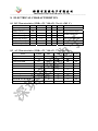
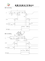
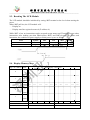
深 圳 市 亚 斌 电 子 有 限 公 司
SHENZHEN YABIN ELECTRONICS CO.,LTD
---------------------------------------------------------------------------------------------------------------------------------------------------------
图形点阵液晶显示模块使用手册
YB12864D
LCD MODULE USER MANUAL
地址:深圳市宝安区石岩镇水田社区水田路 18 号亿莱工业
邮编:518108
电 话:0755-29517345
29517346
传 真:0755-29517347
http://www.yab-lcm.com
E-mail:[email protected]
深 圳 市 亚 斌 电 子 有 限 公 司
SHENZHEN YABIN ELECTRONICS CO.,LTD
---------------------------------------------------------------------------------------------------------------------------------------------------------
1. FUNCTIONS & FEATURES
Features
一 Dot Matrix: 128×64 Dots
一 LCD Mode: STN
一 Controller IC: KS0107 or Equivalent
一 Driving Method: 1/64 Duty; 1/9 Bias
一 Viewing Angie: 6 O’clock direction
一 6800 serial 8-Bit MPU Interface
一 Backlight: LED
一 Operating Temperature Range: -20 to 70℃;
一 Storage Temperature Range : -30 to 80℃;
Note: Color tone is slightly changed by temperature and driving voltage.
2. MECHANICAL SPECIFICATIONS
ITEM
SPECIFICATIONS
UNIT
Module Size
93.0L×70.0W×13.0(max)H
mm
70.7×38.8
mm
Effective Area
128×64
dots
Dot Size
0.48×0.48
mm
Dot Pitch
0.52×0.52
mm
View
Area
深 圳 市 亚 斌 电 子 有 限 公 司
SHENZHEN YABIN ELECTRONICS CO.,LTD
---------------------------------------------------------------------------------------------------------------------------------------------------------
3. EXTERNAL DIMENSIONS
93.0± 0.3
88.0
87.2± 0.2
70.7(V.A)
66.52(A.A)
4-? 2.5
4-? 5.0PAD
MAX13.0
9.0± 0.3
0.04
0.48
70.0± 0.3
65.0
53.5± 0.2
38.8(V.A)
33.24(A.A)
0.48
0.04
1
2.5
8.25
15.6
18.38
20
14.0
@2.54x19=48.26
? 1.0
1.6
深 圳 市 亚 斌 电 子 有 限 公 司
SHENZHEN YABIN ELECTRONICS CO.,LTD
---------------------------------------------------------------------------------------------------------------------------------------------------------
4. BLOCK DIAGRAM
KS0107 64COM
or Eqv
LCD PANEL
128x64 dots
64SEG
VDD
VSS
V0
VOUT
DC/DC
Converter
KS0108
or Eqv
64SEG
KS0108
or Eqv
DB0-DB7
RS,R/W,E,/RST
CS1
CS2
LEDA
LEDK
5. POWER SUPPLY
LED Backlight
深 圳 市 亚 斌 电 子 有 限 公 司
SHENZHEN YABIN ELECTRONICS CO.,LTD
---------------------------------------------------------------------------------------------------------------------------------------------------------
6. PIN DESCRIPTION
ITEM
SYMBOL
LEVEL
FUNCTION
1
VSS
0V
2
VDD
5.0V
3
V0
—
4
RS
H/L
H:Data
L:Command
5
R/W
H/L
H:Read
L:Write
6
E
H,H->L
7
~
14
DB0
~
DB7
H/L
15
CS1
L
Chip Selection A
16
CS2
L
Chip Selection B
17
/RST
L
Reset Signal
18
Vout
—
Negative Power output For LCD Driving
19
LEDA
5.0V
20
LEDK
0V
Power Ground
Power Supply For Logic
Contrast Adjust
Enable Signal
Data Bus
Power Supply For LED Backlight
7. MAXIMUM ABSOLUTE LIMIT (T=25°C)
Items
Symbol
Standard Value
Unit
Supply Voltage
Vdd
-0.3~7.0
V
Input Voltage
Vin
Vss~Vdd
V
Operating Temperature
Top
-20~70
℃
Storage Temperature
Tst
-30~80
℃
Note: Voltage greater than above may damage the module
All voltages are specified relative to VSS=0V
深 圳 市 亚 斌 电 子 有 限 公 司
SHENZHEN YABIN ELECTRONICS CO.,LTD
---------------------------------------------------------------------------------------------------------------------------------------------------------
8. ELECTRICAL CHARACTERISTICS
8.1 DC Characteristics (VDD=+5V, VSS=0V, Ta=-0~+50°C)
Items
Symbol
Min
TYP
Max
Unit
Condition
Operating Voltage
Vdd
4.8
5.0
5.2
V
Supply Current
Idd
—
8
15
mA
Input High Voltage
Vin
2.0
—
Vdd
V
Input Low Voltage
Vil
0
—
0.8
V
Output High Voltage
Voh
2.4
—
—
V
Ioh=-0.1mA,DB0-DB7
Output Low Voltage
Vol
—
—
0.4
V
Iol=0.1mA,DB0-DB7
LCD Driving Voltage
Vlcd
9.7
10.0
10.3
V
Vdd-V0
Vdd
except LED backlight
RS,RW,E,DB0-DB7
8.2 AC Characteristics (VDD=+5V, VSS=0V, TTa=-20~75°)
Items
Symbol
Min
TYP
Max
Unit
tC
1000
—
—
nS
E high level width
tWH
450
—
—
nS
E low level width
tWL
450
—
—
nS
E rise time
tR
—
—
25
nS
E fall time
tF
—
—
25
nS
Address set-up time
tASU
140
—
—
nS
Address hold time
tAH
10
—
—
nS
Data set-up time
tDSU
200
—
—
nS
Data delay time
tD
—
—
320
nS
Data hold time(write)
tDHW
10
—
—
nS
Data hold time(read)
tDHR
20
—
—
nS
E cycle time
深 圳 市 亚 斌 电 子 有 限 公 司
SHENZHEN YABIN ELECTRONICS CO.,LTD
---------------------------------------------------------------------------------------------------------------------------------------------------------
MPU write timing
MPU read timing
深 圳 市 亚 斌 电 子 有 限 公 司
SHENZHEN YABIN ELECTRONICS CO.,LTD
---------------------------------------------------------------------------------------------------------------------------------------------------------
9. FUNCTION SPECIFICATIONS
9.1. Basic Setting
To drive the LCD module correctly and provide normally display, please use the following
setting:
一 Display start line(Z address)=0;
一 LCD display=ON.
Note:
一 These setting/commands should issue to both controllers while start up;
一 See the Display control instructions section for details.
9.2. Adjusting The LCD Display Contrast
A Variable-Resistor must be connected to the LCD module for providing a reference to V0.The
recommended value of the Variable-Resistor is 20K to 50K.
深 圳 市 亚 斌 电 子 有 限 公 司
SHENZHEN YABIN ELECTRONICS CO.,LTD
---------------------------------------------------------------------------------------------------------------------------------------------------------
9.3. Resetting The LCD Module
The LCD module should be initialized by setting /RST terminal at low level when turning the
power.
When /RST pull low, the LCD module will:
一 Display on
一 Display start line register becomes 0.(Z-address=0)
While /RST is low, no instructions can be accepted except status read. Therefore execute other
instructions after making sure that DB4=0(clear /RST) and DB7=0(ready) by status read
instruction, the condition of power supply at initial power up are as follow:
Items
Symbol
Min
TYP
Max
Unit
Reset time
trs
2.0
—
—
uS
Rise time
tr
—
—
150
nS
9.4. Display Memory Map
Page(X)address
Data
0
DB7
|
DB0
1
DB7
|
DB0
···
···
6
DB7
|
DB0
7
DB7
|
DB0
Column driver
LCD Display(font view)
···
···
···
···
···
···
···
···
···
···
Y1
Y2
···
Y63
Y4
Y1
Y2
···
Y63
Y4
Column(Y) address
00h—3Fh
00h—3Fh
Total
64×64dots
64×64dots
深 圳 市 亚 斌 电 子 有 限 公 司
SHENZHEN YABIN ELECTRONICS CO.,LTD
---------------------------------------------------------------------------------------------------------------------------------------------------------
Chip select
CS1=0,CS2=1
CS1=1,CS2=0
Note:
一 Display start line (Z address)=0;
一 The display data store separated in two divers;
一 The display data for the left section could be accessed by setting CS1=0,
The display data for the right section could be accessed by setting CS2=0.
9.5. Internal registers
There are three registers in each section of LCD module. Each of them could be controlled
independently.
9.5.1. Page (X)Address Register
X address register designates pages of internal display data RAM. Count function is not
available. The address should be set by instruction.
9.5.2. Column (Y)Address Register
Y address register designates address of internal display data RAM. It could be set by
instruction and it increased by 1 automatically by read or write display data operations.
9.5.3. Display Start line (Z) Register
Y address register indicates of display data RAM to LCD top line. It may be used for scrolling
the display pattern on the LCD.
深 圳 市 亚 斌 电 子 有 限 公 司
SHENZHEN YABIN ELECTRONICS CO.,LTD
---------------------------------------------------------------------------------------------------------------------------------------------------------
9.6. Display Control Instructions
Note:
1*. Only one section(driver) could be read at the same time.
2*. For the details of the display control instructions, please refer to KS0108B datasheet.
10. DESIGN AND HANDING PRECAUTION
10.1.The LCD panel is made by glass. Any mechanical shock (eg. Dropping form high
place) will damage the LCD module. Do not add excessive force on the surface of the
display, which may cause the Display color change abnormally.
10.2.The polarizer on the LCD is easily get scratched. If possible, do not remove the LCD
protective film until the last step of installation.
10.3.Never attempt to disassemble or rework the LCD module.
10.4.Only Clean the LCD with Isopropyl Alcohol or Ethyl Alcohol. Other solvents (eg.
water) may damage the LCD.
10.5.When mounting the LCD module, make sure that it is free form twisting, warping and
distortion.
10.6.Ensure to provide enough space(with cushion) between case and LCD panel to
prevent external force adding on it, or it may cause damage to the LCD or degrade the
display result
10.7.Only hold the LCD module by its side. Never hold LCD module by add force on the
heat seal or TAB.
10.8.Never add force to component of the LCD module. It may cause invisible damage or
degrade of the reliability.
深 圳 市 亚 斌 电 子 有 限 公 司
SHENZHEN YABIN ELECTRONICS CO.,LTD
---------------------------------------------------------------------------------------------------------------------------------------------------------
10.9.LCD module could be easily damaged by static electricity. Be careful to maintain an
optimum anti-static work environment to protect the LCD module.
10.10. When peeling of the protective film form LCD, static charge may cause abnormal
display pattern. It is normal and will resume to normal in a short while.
10.11. Take care and prevent get hurt by the LCD panel edge.
10.12. Never operate the LCD module exceed the absolute maximum ratings.
10.13. Keep the signal line as short as possible to prevent noisy signal applying to LCD
module.
10.14. Never apply signal to the LCD module without power supply.
10.15. IC chip (eg. TAB or COG) is sensitive to the light. Strong lighting environment
could possibly cause malfunction. Light sealing structure casing is recommend.
10.16. LCD module reliability may be reduced by temperature shock.
10.17. When storing the LCD module, avoid exposure to the direct sunlight, high
humidity, high temperature or low temperature. They may damage or degrade the LCD
module