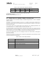
1
Technical
Information
Manual
Revision n. 4
26 January 2007
MOD. N568 B
MOD. N568 LC
16 CHANNEL
Spectroscopy Amplifiers
CAEN will repair or replace any product within the guarantee period if the Guarantor declares that the
product is defective due to workmanship or materials and has not been caused by mishandling,
negligence on behalf of the User, accident or any abnormal conditions or operations.
CAEN declines all responsibility for damages or injuries
caused by an improper use of the Modules due to
negligence on behalf of the User. It is strongly
recommended to read thoroughly the CAEN User's Manual
before any kind of operation.
CAEN reserves the right to change partially or entirely the contents of this Manual at any time and
without giving any notice.
Disposal of the Product
The product must never be dumped in the Municipal Waste. Please check your local regulations for
disposal of electronics products.
Document type:
User's Manual (MUT)
Title:
Mod. N568B/LC 16 Ch Spectroscopy Amplifiers
Revision date:
26/01/2007
Revision:
4
TABLE OF CONTENTS
1.
DESCRIPTION ...........................................................................................................................................6
1.1
2.
3.
SPECIFICATIONS .....................................................................................................................................8
2.1
EXTERNAL COMPONENTS..............................................................................................................8
2.2
CHARACTERISTICS OF THE SIGNALS ..........................................................................................9
2.3
POWER REQUIREMENTS ...............................................................................................................10
OPERATING MODES .............................................................................................................................12
3.1
GENERAL INFORMATION .............................................................................................................12
3.2
MODULE OPERATION ....................................................................................................................12
3.2.1
MANUAL SETTINGS ..................................................................................................................12
3.2.2
OUTPUT CONFIGURATION SETTING ....................................................................................12
3.2.3
OUTPUT POLARITY SETTING..................................................................................................13
3.2.4
SHAPE SETTING ........................................................................................................................13
3.2.5
GAIN SETTING ...........................................................................................................................14
3.2.6
POLE ZERO ADJUSTMENT ......................................................................................................14
3.2.7
OFFSET SETTING......................................................................................................................14
3.3
4.
FUNCTIONAL DESCRIPTION...........................................................................................................6
H. S. CAENET ....................................................................................................................................15
H. S. CAENET OPERATION..................................................................................................................16
4.1
USING THE H. S. CAENET MANUAL CONTROLLER ................................................................16
4.2
USING THE H. S. CAENET VME CONTROLLER .........................................................................18
4.2.1
Master to Slave data composition (V288 case) ...........................................................................19
4.2.2
Slave to Master data composition (V288 case) ...........................................................................19
4.3
USING THE H. S. CAENET CAMAC CONTROLLER ...................................................................20
4.3.1
Master to Slave data composition (C117B case).........................................................................21
4.3.2
Slave to Master data composition (C117B case).........................................................................21
4.3.3
MASTER TO SLAVE OPERATING CODES (CAMAC and VME)..............................................22
4.4
SET VALUES .....................................................................................................................................22
4.5
SLAVE TO MASTER DATA PACKET DESCRIPTION (CAMAC AND VME) .............................24
4.5.1
Error Codes description ..............................................................................................................25
4.5.2
Module Identifier Packet (response to code %0).........................................................................26
4.6
USING THE H. S. CAENET PC CONTROLLERS...........................................................................26
Filename:
N568B_N568LC_REV4.DOC
Number of pages:
37
Page:
3
Document type:
User's Manual (MUT)
4.7
Title:
Mod. N568B/LC 16 Ch Spectroscopy Amplifiers
Revision date:
26/01/2007
Revision:
4
BOARD CONTROL VIA OPC SERVER ..........................................................................................27
4.7.1
N568B / N568LC board control ..................................................................................................27
4.7.2
N568B / N568LC channel control ...............................................................................................29
4.8
DATA COMPOSITION (PC CONTROLLER CASE).......................................................................31
4.8.1
Master to Slave Data Composition (PC Controller Case) ..........................................................31
4.8.2
Slave to Master Data Composition (PC Controller Case) ..........................................................32
4.9
MASTER TO SLAVE OPERATING CODES (PC CONTROLLER CASE) ....................................32
4.10
SET VALUES .....................................................................................................................................33
4.11
SLAVE TO MASTER DATA PACKET DESCRIPTION (PC CONTROLLER CASE) ..................34
4.11.1
Error Codes description ..............................................................................................................36
4.11.2
Module Identifier Packet (response to code %0).........................................................................36
LIST OF FIGURES
FIG. 1.1: N568B/LC BLOCK DIAGRAM ..............................................................................................................7
FIG. 1.2: N568B/LC CHANNEL BLOCK DIAGRAM .............................................................................................7
FIG. 2.1: MOD. N568B/LC FRONT PANEL .......................................................................................................11
FIG. 3.1: FOUT CONFIGURATION .....................................................................................................................13
FIG. 4.1: MOD. N568B/LC STATUS REGISTER.................................................................................................24
LIST OF TABLES
TABLE 2.1: MOD. N568B/ N568LC TECHNICAL FEATURES ..............................................................................9
TABLE 3.1: GAIN VALUES (SIGNALS RISETIME: 10 µS) ....................................................................................14
TABLE 3.2: GAIN VALUES (SIGNALS RISETIME: 0.05 µS) .................................................................................14
TABLE 4.1: MOD. V288 REGISTERS .................................................................................................................19
TABLE 4.2: MASTER TO SLAVE DATA COMPOSITION (V288 CASE)...................................................................19
TABLE 4.3: SLAVE TO MASTER DATA COMPOSITION (V288 CASE) ...................................................................20
TABLE 4.4: MOD. C 117 B CAMAC FUNCTIONS ............................................................................................20
TABLE 4.5: MASTER TO SLAVE DATA COMPOSITION (C117B CASE) ................................................................21
TABLE 4.6: SLAVE TO MASTER DATA COMPOSITION (C117B CASE) ................................................................21
TABLE 4.7: OPERATING CODES OF THE N568B/LC (C117B AND V288 CASE) ................................................22
TABLE 4.8: COARSE GAIN VALUES ..................................................................................................................23
TABLE 4.9: SHAPE VALUES ..............................................................................................................................23
TABLE 4.10: ERROR CODES (C117B AND V288 CASE) ....................................................................................25
Filename:
N568B_N568LC_REV4.DOC
Number of pages:
37
Page:
4
Document type:
User's Manual (MUT)
Title:
Mod. N568B/LC 16 Ch Spectroscopy Amplifiers
Revision date:
26/01/2007
Revision:
4
TABLE 4.11: MODULE IDENTIFIER DATA PACKET STRUCTURE ........................................................................26
TABLE 4.12: HS CAENET PC CONTROLLERS REGISTERS .........................................................................27
TABLE 4.13– N568B / N568LC BOARD ITEMS................................................................................................28
TABLE 4.14– N568B / N58LC CHANNEL ITEMS ..............................................................................................31
TABLE 4.15: MASTER TO SLAVE DATA COMPOSITION ......................................................................................32
TABLE 4.16: SLAVE TO MASTER DATA COMPOSITION ......................................................................................32
TABLE 4.17: OPERATING CODES OF THE N568B/LC........................................................................................33
TABLE 4.18: COARSE GAIN VALUES ................................................................................................................34
TABLE 4.19: SHAPE VALUES ............................................................................................................................34
TABLE 4.20: ERROR CODES .............................................................................................................................36
TABLE 4.21: MODULE IDENTIFIER DATA PACKET STRUCTURE ........................................................................37
Filename:
N568B_N568LC_REV4.DOC
Number of pages:
37
Page:
5
Document type:
User's Manual (MUT)
Title:
Mod. N568B/LC 16 Ch Spectroscopy Amplifiers
Revision date:
26/01/2007
Revision:
4
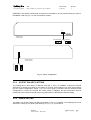
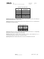
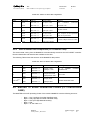
1. DESCRIPTION
1.1
FUNCTIONAL DESCRIPTION
The Model N 568 LC is a 16 CHANNEL SPECTROSCOPY AMPLIFIER implemented in a single-width
NIM module. A “Low Noise1” version, the N568 B2, is also available.
It accepts the typical outputs generated from nuclear particle detectors connected with preamplifiers
having an output signal pulse characterised by a fast rise time and a slow fall time. With 16
independent channels, this unit allows the optimization of cost and size in multi-detector systems.
For each channel the pole-zero cancellation (PZ), the shaping time, the amplification gain and the
output inversion are remotely programmable (by CAMAC, VME, Standard PC or Manual Controller)
via HIGH SPEED CAENET line.
The shaping time can be selected from 0.2 µs to 6 µs. The fine gain and coarse gain ranges allow a
choice accuracy from 0.15 to 480. The working parameter values are automatically stored in a nonvolatile memory. The inputs and the outputs of this module are accessible on the front panel.
A Gaussian Output is provided either with the programmed gain (OUT) or with a further 10x
amplification (XOUT). The Gaussian Output can be set either as inverted or non-inverted.
A COMMON OFFSET can be programmed via CAENET and allows to shift the baseline of the output.
An FOUT output provides a fast amplification for timing purposes (fixed gain factor of 20). A "MUX O"
and a "MUX F" output allow to monitor respectively the output and the fast output of a single channel
selected via CAENET.
Two LEMO 00 connectors are foreseen for the CAENET line and a LED indicates the electrical
condition of the CAENET network. When several modules are connected to the CAENET network,
their identification is obtained by the thumb-wheel switches located on the front panel: up to 99 N 568
B/LC modules are controlled via 50 Ω coaxial cable at 1 MB transmission speed. Allowed controllers
are the Manual Controller (Mod. A 250), the CAMAC (Mod. C 117 B), the VME (Mod. V 288) or the
Standard PC (Mod. A 303, A303A and A1303) H. S. CAENET Controllers.
The communication between the Host computer system and the HIGH SPEED CAENET controller is
performed via standard functions and cycles (CAMAC and VME systems) or via a standard memory
or I/O mapped mode for a standard PC (for more detailed information see the relevant Technical
Information Manual). The communication protocol and the meaning of the recognized command
codes are always the same, independently from the used controller.
The performances of this module allow operation with scintillation detectors, proportional counters,
semiconductor detectors in different applications.
1
Equivalent input noise < 15 µV RMS (Gain=100 and 3 µs shaping time)
2
Mod. N568 B Designed in collaboration with the I.N.F.N. MILANO
Filename:
N568B_N568LC_REV4.DOC
Number of pages:
37
Page:
6
Document type:
User's Manual (MUT)
Title:
Mod. N568B/LC 16 Ch Spectroscopy Amplifiers
IN0
SERIAL
Revision date:
26/01/2007
IN
CONTROL CHANNEL
VOFFSET
POWER SUPPLY
IN1
IN
CONTROL CHANNEL
VOFFSET
POWER SUPPLY
IN14
IN
CONTROL CHANNEL
VOFFSET
POWER SUPPLY
IN15
IN
CONTROL CHANNEL
VOFFSET
POWER SUPPLY
Revision:
4
OUT
OUT x10
MUX O
FAST OUT
MUX F
0
OUT
OUT
OUT x10
MUX O
FAST OUT
MUX F
1
14
15
OUT
OUT x10
MUX O
FAST OUT
MUX F
XOUT
OUT
OUT x10
MUX O
FAST OUT
MUX F
MUX O
MUX F
CONTROL
LOGIC
FAST
AMP
IN/OUT
FAST
OUT
POWER
SUPPLY
Fig. 1.1: N568B/LC Block Diagram
INPUT
INV
BUFF
FAST OUT
FAST
AMP
MUX F
x10
GAIN
SHAPING
TIME 1
P/Z
CANC
SHAPING
TIME 2
MUX
COARSE
GAIN
FINE
GAIN
OUT
CONF.
XOUT
OUT
BLR
SHAPING
TIME 3
SHAPING
TIME 4
MUX O
CONTROL
CONTROL BUS
LOGIC
VOFFSET
Fig. 1.2: N568B/LC Channel Block Diagram
Filename:
N568B_N568LC_REV4.DOC
Number of pages:
37
Page:
7
Document type:
User's Manual (MUT)
Title:
Mod. N568B/LC 16 Ch Spectroscopy Amplifiers
Revision date:
26/01/2007
Revision:
4
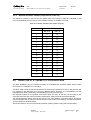
2. SPECIFICATIONS
2.1
EXTERNAL COMPONENTS
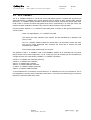
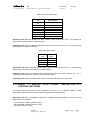
CONNECTORS
- N. 16, "INPUTS 0..15", LEMO 00 type; input signal connectors.
- N. 1, "MUX O", LEMO 00 type; single selected channel output connector.
- N. 1, "MUX F", LEMO 00 type; single selected channel output connector.
- N. 1, "OUT 0..15", output connector, 17+17 pin, double row strip header (left pin: ground, right pin.
signal).
- N. 1, "XOUT 0..15", output connector, 17+17 pin, double row strip header (left pin: ground, right pin:
signal).
- N. 1, "FOUT 0..15", output connector, 17+17 pin, double row strip header (left pin: ground, right pin:
signal).
- N. 2, "HIGH SPEED CAENET - SERIAL IN/OUT", LEMO 00 type, high impedance. Connectors for
the HIGH SPEED CAENET operations.
- N. 1, "PWR MAN CTR", coaxial female plug, RCA type, to power the H. S. CAENET Manual
Controller.
DISPLAYS
- N. 1, red LED, to indicate the activity of the H. S. CAENET node.
SWITCHES, TEST POINTS
- N. 1, "STATION NUMBER", Thumb-wheel switch selector, for the selection of the module
identification (station number).
- N. 16, "INPUTS 0..15", input signal test points.
Filename:
N568B_N568LC_REV4.DOC
Number of pages:
37
Page:
8
Document type:
User's Manual (MUT)
2.2
Title:
Mod. N568B/LC 16 Ch Spectroscopy Amplifiers
Revision date:
26/01/2007
Revision:
4
CHARACTERISTICS OF THE SIGNALS
Table 2.1: Mod. N568B/ N568LC Technical Features
NAME
N568B
N568LC
INPUTS
INPUTS 0..15
Positive or negative pulses with rise time ≥18 ns, max. amplitude: 8 V (absolute
value); 50 Ω impedance
H. S. CAENET IN/OUT
Std. CAENET protocol signals
OUTPUTS
OUT
100 Ω impedance. Unipolar, dynamic range ±8 V max (1 Mohm load); polarity
as selected in common with XOUT and MUXOUT.
XOUT
100 Ω impedance. Unipolar, further 10x fixed amplification of the OUT value,
dynamic range ±4 V max into 100 Ω load; polarity as selected in common with
OUT and MUXOUT.
FOUT
100 Ω impedance. Unipolar, 100 ns
Differentiation Time Constant, ±4 V
max into 100 Ω load. Risetime: 25 ns
typically.
Gain factor: 7 to 10 for non inverting
configuration, 20 to 30 (approx.) for
inverting configuration.
MUX O
100 Ω impedance. Unipolar, ±8 V max (1 Mohm load); polarity as selected in
common with OUT. Selected channel is the last accessed via H.S. CAENET.
Can be disabled via CAENET.
MUX F
100 Ω impedance. Unipolar, amplitude 85% approx. of FOUT amplitude.
Selected channel is the last accessed via H.S. CAENET. Can be disabled via
CAENET.
PWR MAN CTR
Std. CAENET Manual Controller supply voltage
50 Ω impedance. Unipolar, 100 ns
Differentiation Time Constant, ±4 V
max into 100 Ω load. Risetime: 25 ns
typically.
Gain factor: 7 to 10 for both inverting
and non inverting configuration
GENERAL
INTEGRAL NON
LINEARITY
±0.05% in 90% of the full scale @ Gain=90 and 6 µs shaping time (± 0.25%
typ. for any shaping time)
EQUIVALENT INPUT
NOISE
< 15 µV (Gain=100; 3 µs shaping time)
INTERCHANNEL
CROSSTALK
Output in one OUT (FOUT) channel affects any other OUT (FOUT) channel by
no more than -45 dB (at Gain =1 and 5 V input signal)
GAIN RANGE
adjustable from 0.15 to 480 (see § 3.2.5)
SHAPING TIME
selectable time constant of 0.2 µs, 1 µs, 3 µs and 6 µs
COMMON OFFSET
from -75 mV to +210 mV with Positive Output Polarity; from +75 mV to -210
mV with Negative Output Polarity
POLE ZERO
adjustable on 256 steps to match preamp tails in a range from 50 µs to 500 µs
Filename:
N568B_N568LC_REV4.DOC
< 25 µV (Gain=100; 3 µs shaping
time)
Number of pages:
37
Page:
9
Document type:
User's Manual (MUT)
2.3
Title:
Mod. N568B/LC 16 Ch Spectroscopy Amplifiers
Revision date:
26/01/2007
Revision:
4
POWER REQUIREMENTS
+ 12 V
- 12 V
+6V
2300 mA Maximum (inputs on all 16 channels)
1050 mA
750 mA (1100 mA with A250 MAN. CONT. plugged in)
Filename:
N568B_N568LC_REV4.DOC
Number of pages:
37
Page:
10
Document type:
User's Manual (MUT)
Title:
Mod. N568B/LC 16 Ch Spectroscopy Amplifiers
Revision date:
26/01/2007
Revision:
4
16 CH SPECTROSCOPY
AMPLIFIER
Mod. V560E
M o d . N 568 B
15
OUTPUTS
15
X
O
U
T
O
U
T
0
10x OUTPUTS
0
0
M
U
X
1
F
MULTIPLEX OUTPUTS
O
15
2
3
4
F
O
U
T
5
FAST OUTPUTS
6
INPUTS AND TEST POINTS 0..15
7
8
0
9
HIGH
CAENE
10
I
N
/
O
U
T
S
E
R
I
A
L
11
12
13
H. S. CAENET CONNECTORS
14
POWER OUT FOR
15
−
STATION NUMBER
SELECTOR
1
PWR MAN CTR
MANUAL CONTROLLER
−
8
+ +
STATION
16 CH
SCALER
Fig. 2.1: Mod. N568B/LC Front Panel
Filename:
N568B_N568LC_REV4.DOC
Number of pages:
37
Page:
11
Document type:
User's Manual (MUT)
Title:
Mod. N568B/LC 16 Ch Spectroscopy Amplifiers
Revision date:
26/01/2007
Revision:
4
3. OPERATING MODES
3.1
GENERAL INFORMATION
The Model N 568B/LC is a 16 CHANNEL SPECTROSCOPY AMPLIFIER implemented in a singlewidth NIM module.
Thanks to its high channel density, this unit allows the optimization of cost and size in multi-detector
systems.
3.2
MODULE OPERATION
At Power-ON, the module contains the last performed settings before Power-Off. The status of these
settings can be read out via H.S. CAENET (see below).
The settings on each channel of the module can be performed in any order. Due to the logical
dependence of certain settings from others, it is anyhow suggested to perform the first time User'
settings on each channel of the module in the following order:
a) set the output configuration (non-inverting or inverting);
b) set the output polarity (positive or negative);
c) set the shape;
d) set the coarse gain;
e) set the fine gain;
f) set the pole-zero adjustment;
g) set the offset;
h) enable or disable the multiplexed output.
Once performed either first-time or ordinary settings, it is suggested, for best noise performances,
NOT to access the module frequently via H.S. CAENET (e.g. for monitoring) while the module is
operating on the final experimental setup.
The following paragraphs describe in more detail the single settings. Offset, Fine Gain and Pole-zero
settings must be thought not as absolute settings, but as "digital trimmers" with which the User sets
the desired parameters and controls the outputs obtained with well-known pulse shapes.
3.2.1
MANUAL SETTINGS
A two-digit thumb-wheel switch selects the module's Station Number for the CAENET operations.
3.2.2
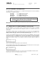
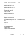
OUTPUT CONFIGURATION SETTING
The OUT and XOUT configuration settings can be performed either via Manual Controller or via H. S.
CAENET. They allow to select between DIRECT (NON-INVERTED) or INVERTED outputs. The
FOUT configuration can be selected between DIRECT (NON-INVERTED, factory setting) or
Filename:
N568B_N568LC_REV4.DOC
Number of pages:
37
Page:
12
Document type:
User's Manual (MUT)
Title:
Mod. N568B/LC 16 Ch Spectroscopy Amplifiers
Revision date:
26/01/2007
Revision:
4
INVERTED. The setting is performed via jumper for the N568 LC and by shortcircuiting two pins for
the N568 B; refer to Fig. 3.1 for the components’ location.
S1
+
-
FPOLSEL
N568B channel
(soldering side)
NON-INVERTING
+
-
INVERTING
+
-
J2
INVERTING
NON-INVERTING
N568LC channel
(components side)
Fig. 3.1: FOUT configuration
3.2.3
OUTPUT POLARITY SETTING
This setting can be done either via Manual Controller or via H. S. CAENET. It allows the internal
electronics to operate at its best on the signals. It must be set according to the input signal polarity
and the output configuration setting, e.g. if the input signal is Positive and the desired Output
Configuration is chosen as Inverted, the output polarity is Negative and this information must be
transferred to the module's internal electronics (optimization of the Baseline Restorer stage).
3.2.4
SHAPE SETTING
This setting can be done either via Manual Controller or via H. S. CAENET. The shaping time can be
selected in 4 steps (0 to 3) among the following: 0.2 µs, 1 µs, 3 µs and 6 µs.
Filename:
N568B_N568LC_REV4.DOC
Number of pages:
37
Page:
13
Document type:
User's Manual (MUT)
3.2.5
Title:
Mod. N568B/LC 16 Ch Spectroscopy Amplifiers
Revision date:
26/01/2007
Revision:
4
GAIN SETTING
This setting can be done either via Manual Controller or via H. S. CAENET. The Coarse Gain can be
set in 8 steps (0 to 7), each step approximately doubling the Gain of the previous one. The Fine Gain
can be set in 255 steps (0 to 255). The fine gain and coarse gain ranges allow a choice accuracy from
0.15 to 480. As an example, the following tables contain some extremity gain values obtained with the
indicated shaping times and gain settings (positive input signals).
Table 3.1: Gain Values (Signals risetime: 10 µs)
Gain values
Shape
Times
Coarse
Gain
0
7
0.2 µs
(Input Signals risetime: 10 µs)
1 µs
3 µs
Fine Gain
0
255
Fine Gain
0
255
0.15
0.6
Fine Gain
0
255
1.13
38.02
153.64
6 µs
Fine Gain
0
255
1.25
286.45
322.91
Table 3.2: Gain Values (Signals risetime: 0.05 µs)
Gain values
Shape
Times
Coarse
Gain
0
7
3.2.6
0.2 µs
(input Signals risetime: 0.05 µs)
1 µs
3 µs
Fine Gain
0
255
1.25
Fine Gain
0
255
1.88
260.41
Fine Gain
0
255
1.86
476.56
6 µs
Fine Gain
0
255
1.6
481.77
416.6
POLE ZERO ADJUSTMENT
This setting can be done either via Manual Controller or via H. S. CAENET. Adjustable on 256 steps
to match preamp tails in a range from 50 µs to 500 µs.
3.2.7
OFFSET SETTING
This setting can be done either via Manual Controller or via H. S. CAENET. Allows to add an offset
value to shift the baseline of the output. Allowed values are from -75 mV to +210 mV with Positive
Output Polarity; from +75 mV to -210 mV with Negative Output Polarity.
Filename:
N568B_N568LC_REV4.DOC
Number of pages:
37
Page:
14
Document type:
User's Manual (MUT)
3.3
Title:
Mod. N568B/LC 16 Ch Spectroscopy Amplifiers
Revision date:
26/01/2007
Revision:
4
H. S. CAENET
The H. S. CAENET Network is a send and receive half duplex system; It enables the asynchronous
serial transmission (1 MBaud rate) of data packets along a simple 50 Ohm coaxial cable. Several
devices (H. S. CAENET nodes) are able to share the same media to transmit and receive data. Each
node is able to receive the serial data packet and store it automatically in a FIFO (RX FIFO) and
transmit the data contained in another FIFO (TX FIFO). Both FIFOs are 512 byte deep.
Usually transfers between H. S. CAENET nodes take place according to the typical Master/Slaves
communication:
- There is a single Master : H. S. CAENET controller
- The Slaves are daisy chained on the network, and are identified by an address code
(from 1 to 99);
- the H. S. CAENET Master initiates the transmission, all the Slaves receive the data,
and only the Slave addressed then accesses the serial line to transmit the data
requested by the Master.
- The maximum data packet length is 512 bytes.
The address of the H. S. CAENET node of the N568B/LC (Station #) is selectable via front panel
thumb-wheels, and its value ranges from 1 to 99. In this way up to 99 modules may be controlled from
a single point via one of the following CAEN H. S. CAENET Controllers:
A1303 H. S. CAENET PC Controller (PCI bus);
A303A H. S. CAENET PC Controller;
A303 H. S. CAENET PC Controller;
A250 H. S. CAENET Manual Controller;
C117B H. S. CAENET CAMAC Controller;
V288 H. S. CAENET VME Controller.
To avoid reflections it is necessary to terminate the H. S. CAENET line on a 50 Ω impedance. This is
accomplished by inserting a 50 Ω impedance terminator in one of the two LEMO 00 type connectors
(IN/OUT) of the last module of the chain.
Filename:
N568B_N568LC_REV4.DOC
Number of pages:
37
Page:
15
Document type:
User's Manual (MUT)
Title:
Mod. N568B/LC 16 Ch Spectroscopy Amplifiers
Revision date:
26/01/2007
Revision:
4
4. H. S. CAENET OPERATION
The Model N568B/LC is provided with an H. S. CAENET node through which it can be controlled by
the following H. S. CAENET Controllers:
Mod. A250
Mod. V288
Mod. C117B
Mod. A303
- H. S. CAENET Manual Controller;
- H. S. CAENET VME Controller;
- H. S. CAENET CAMAC Controller;
- H. S. CAENET PC Controller.
NOTE: the address number of the N568B/LC (Station #) must be the
only one in the line in which you wish to insert the module. Due to high
transmission speed of the data in line it is necessary to terminate this
line on a 50 Ω impedance at the end to avoid reflections.
Via H. S. CAENET it is possible to select the desired output channel, that will thus provide the same
input signal.
4.1
USING THE H. S. CAENET MANUAL CONTROLLER
The Mod. N568B/LC can be controlled remotely via VME through the Mod. A250 H. S. CAENET
Manual Controller. The Mod. A250 has been designed to control a H. S. CAENET node via 50 Ω
coaxial cable.
The sequence of display pages in the Manual Controller is not exactly as in the suggested firstsettings procedure (see § 3.2), but after a first setting is performed, the first page appearing in the
Display is the Gain setting page, which is the most frequently accessed page.
In order to use the Manual Controller, the User must connect it to the N568B/LC, using a 50 Ohm
coaxial cable into the "H. S. CAENET IN/OUT" connectors of the N568B/LC; the supply of the Manual
Controller is provided from the N568B/LC front panel via suitable cable (RCA connectors) supplied by
CAEN with the Manual Controller. Once supplied, the Manual Controller's display will appear as
follows:
CAEN A250
Select Cr.
1.0
**
where 1.0 is the Firmware release version of the Controller itself.
Type the address number of the module, previously set via thumb-wheel switch on the front panel,
and confirm the choice with the key "#". The display will show:
AA
Software
N568 Version x.x
where AA is the selected address number. The version number is the N568B/LC Firmware version.
By pressing the "PAGE" key, the display will appear as follows:
Filename:
N568B_N568LC_REV4.DOC
Number of pages:
37
Page:
16
Document type:
User's Manual (MUT)
AA Ch** Fg
N568
Title:
Mod. N568B/LC 16 Ch Spectroscopy Amplifiers
Revision date:
26/01/2007
Revision:
4
NNN
Cg
M
where AA is still the selected address number. The address number starts blinking, indicating the
currently modifiable field. By pressing the key "#", the blinking can be moved on the Ch (Channel
Number) field: by pressing "ROLL" it is possible to increment the value of the Channel Number by 1
(Channel values: 0 to 15). This number indicates the Channel on which all following settings are
performed. By pressing the key "#" the blinking toggles to the Fg (Fine Gain) field in the display (NNN
in the figure above): by pressing "0" or "1" it is possible respectively to decrement/increment the value
of the Fine Gain by 1, while by pressing "4" or "7" it is possible respectively to decrement/increment
the value of the Fine Gain by 10 (allowed Fine Gain values: 0 to 255). By pressing the key "#" the
blinking toggles to the Cg (Coarse Gain) field in the display (M in the figure above): by pressing
"ROLL" it is possible to increment the value of the Coarse Gain by 1 (allowed Coarse Gain values: 0
to 7).
By pressing the "PAGE" key, the display will appear as follows:
AA Ch** PZ
N568
NNN
Sh
L
where AA is the selected address number. By pressing the key "#" the blinking toggles from the
position of the blinking field in the previous page to the following at its right. By pressing the key "#",
the blinking can be moved on the Ch (Channel Number) field: by pressing "ROLL" it is possible to
increment the value of the Channel Number by 1 (Channel values: 0 to 15). This number indicates the
Channel on which all following settings are performed. By pressing the key "#" the blinking toggles to
the PZ (Pole Zero adjustment) field in the display (NNN in the figure above): by pressing "0" or "1" it is
possible respectively to decrement/increment the value of the Pole Zero adj. by 1, while by pressing
"4" or "7" it is possible respectively to decrement/increment the value of the Pole Zero adj. by 10
(allowed Pole Zero adj. values: 0 to 255). By pressing the key "#" the blinking toggles to the Sh
(Shaping Time) field in the display (L in the figure above): by pressing "ROLL" it is possible to
increment the value of the Shaping Time by 1 (allowed Shaping Time values: 0 to 3).
By pressing the "PAGE" key, the display will appear as follows:
AA Ch** Out Pos
N568
Out NInv
where AA is the selected address number. By pressing the key "#" the blinking toggles from the
position of the blinking field in the previous page to the following at its right. By pressing the key "#",
the blinking can be moved on the Ch (Channel Number) field: by pressing "ROLL" it is possible to
increment the value of the Channel Number by 1 (Channel values: 0 to 15). This number indicates the
Channel on which all following settings are performed. By pressing the key "#" the blinking toggles to
the higher row OUT (Output Polarity) field in the display (Pos in the figure above): by pressing "ROLL"
it is possible to switch from Positive (Pos) to Negative (Neg) polarity. By pressing the key "#" the
blinking toggles to the lower row OUT (Output configuration) field in the display (Ninv in the figure
above): by pressing "ROLL" it is possible to switch from Non-inverting (Ninv) to Inverting (Inv)
configuration.
By pressing the "PAGE" key, the display will appear as follows:
Filename:
N568B_N568LC_REV4.DOC
Number of pages:
37
Page:
17
Document type:
User's Manual (MUT)
Title:
Mod. N568B/LC 16 Ch Spectroscopy Amplifiers
AA
Offset
N568
NNN
Revision date:
26/01/2007
Revision:
4
where AA is the selected address number. By pressing the key "#" the blinking toggles from the
position of the blinking field in the previous page to the following at its right. By pressing the key "#"
the blinking toggles to the Offset (Offset adjustment) field in the display (NNN in the figure above): by
pressing "0" or "1" it is possible respectively to decrement/increment the value of the Offset adj. by 1,
while by pressing "4" or "7" it is possible respectively to decrement/increment the value of the Offset
adj. by 10 (allowed Offset adj. values: 0 to 255). The Offset is the same for all Channels.
By pressing the "PAGE" key, the display will appear as follows:
AA
Mux Out
N568
XXXXXXXX
where AA is the selected address number. By pressing the key "#" the blinking toggles from the
position of the blinking field in the previous page to the following at its right. By pressing the key
"ENTER" it is possible to disable or enable the Multiplexed Outputs. The status of the Multiplexed
Outputs will appear in the XXXXXXXX field ("Disabled" or "Enabled").
4.2
USING THE H. S. CAENET VME CONTROLLER
The Mod. N568B/LC can be controlled remotely via VME through the Mod. V 288 H. S. CAENET VME
Controller.
The Model V288 has been designed to control an H. S. CAENET node through the VME bus. It is
composed of a collection of registers, for the operation control, and two memory buffers for the
transmitted and received data packets, arranged in a FIFO logic 16 bit wide 256 words deep. In the
memory buffer for the received data are also stored the error messages generated by the V288 itself
when the H. S. CAENET operation has failed.
Standard VME cycles allow the User to perform the required control and setting operations on each
Mod. N568B/LC in the network, according to the typical MASTER/SLAVE communication protocol,
where the VME controller assumes the MASTER function. The module's operations can be software
controlled in polling mode or can be handled via interrupt facility. It houses a VME ROAK
INTERRUPTER that generates a VME interrupt (if enabled) as soon as the data packet (or the error
message) is stored in the receive buffer.
The Registers of the Mod. V288 are described in the Table 4.1.
Filename:
N568B_N568LC_REV4.DOC
Number of pages:
37
Page:
18
Document type:
User's Manual (MUT)
Title:
Mod. N568B/LC 16 Ch Spectroscopy Amplifiers
Revision date:
26/01/2007
Revision:
4
Table 4.1: Mod. V288 Registers
NAME
Transmit Data Buffer
Receive Data Buffer
TYPE
Write only
Read
only
Read
only
ADDRESS
Base Address + %00
Base Address + %00
FUNCTION
Transmit data storage
Receive data storage
Base Address + %02
Transmission Register
Write only
Base Address + %04
Reset Register
Interrupt Vector
Register
Write only
Write only
Base Address + %06
Base Address + %08
After an H. S. CAENET operation has
been performed, This register indicates
whether the operation is valid or not
FFFE= valid operation
FFFF= no valid operation
By writing into this register the Transmit
Data buffer content is transmitted on the
cable
Module's Reset
Interrupt vector programming register
Status Register
4.2.1
Master to Slave data composition (V288 case)
The Master to Slave data have to be written in the Transmit Data Buffer, by performing subsequent
write accesses as follows:
Table 4.2: Master to Slave data composition (V288 case)
Order
1
2
3
4
Operation
Write
Write
Write
Write
Address
Base Ad. + 0
Base Ad. + 0
Base Ad. + 0
Base Ad. + 0
Datum (HEX)
%0001
%00XX
Code
Code/Set
Meaning
H. S. CAENET Controller identified code
Module Number
First word of the Operation Code to be performed
Possible subsequent word of the Set value
As soon as the data packet has been stored in the Transmit Data Buffer, it can be transmitted on the
cable by performing a Write operation on the Transmission Register. The Operation Codes are shown
in Tab. 4.7.
After a transmission, in the V288 Receive Data Buffer the User reads the Slave response or a V288
error message (e. g., if the V288 does not receive any Slave response within a period of 500 msec it
stores the code %FFFF in the Receive Data Buffer, see Table 4.10).
4.2.2
Slave to Master data composition (V288 case)
The answer data coming from the Mod. N568B/LC or a Mod. V288 error message are automatically
stored into the V288 Receive Data buffer and therefore are available to the User. As soon as the data
packet is stored in this buffer, a VME interrupt (if enabled) is generated.
The following Table shows the structure of the N568B/LC data packet:
Filename:
N568B_N568LC_REV4.DOC
Number of pages:
37
Page:
19
Document type:
User's Manual (MUT)
Title:
Mod. N568B/LC 16 Ch Spectroscopy Amplifiers
Revision date:
26/01/2007
Revision:
4
Table 4.3: Slave to Master data composition (V288 case)
Order
Operation
Address
Datum
Meaning
1
Read
Base Ad. + 0
Error Code
Error code
2 to 50(*)
Read
Base Ad. + 0
value
Possible Parameter values
(*) The first data of the packet is read and checked by the V288 Control Logic
(see V288 User's Manual ).
The Error Codes are described in Tab. 4.10.
4.3
USING THE H. S. CAENET CAMAC CONTROLLER
The Mod. N568B/LC can be controlled remotely via CAMAC through the Mod. C 117B H. S. CAENET
CAMAC Controller.
The Model C 117B has been designed to control an H. S. CAENET node through the CAMAC bus. It
houses two memory buffers for the transmitted and received data packet, arranged in a FIFO logic 16
bit wide 256 words deep.
In the memory buffer for the received data are also stored the error messages generated by the
C117B itself when the H. S. CAENET operation has failed (see Table 4.10).
The standard CAMAC functions listed in Table 4.4 allow the User to perform the required control and
setting operations on each Mod. N568B/LC in the network according to the typical MASTER/SLAVE
communication protocol, where the CAMAC controller assumes the MASTER function.
As soon as the data packet (or the error message) is stored in the receive buffer, a LAM signal is
generated (if enabled).
X response is generated for all valid function. Q response is generated for each valid function unless
is otherwise specified (see Table below).
Table 4.4: Mod. C 117 B CAMAC Functions
F(0) N
F(8) N
F(9) N
F(16) N
F(17) N
F(24) N
F(26) N
C, Z
Reads the data stored in the mod. C 117 B Receive Data buffer. Q response
while the buffer contains data.
Tests the LAM line. Q response if LAM is true.
Resets the module (clears buffer and LAM; disables the LAM line).
Stores the data into the Mod. C 117 B Transmit Data buffer. Q response until
the buffer is full (256 16-bit words).
Transfers data to the serial line.
Disables the LAM line.
Enables the LAM line.
Same as F(9) N.
Filename:
N568B_N568LC_REV4.DOC
Number of pages:
37
Page:
20
Document type:
User's Manual (MUT)
4.3.1
Title:
Mod. N568B/LC 16 Ch Spectroscopy Amplifiers
Revision date:
26/01/2007
Revision:
4
Master to Slave data composition (C117B case)
The MASTER-to-SLAVE data have to be written into the Transmit Data buffer by performing
subsequent F(16) N functions as follows:
Table 4.5: Master to Slave data composition (C117B case)
Order
1
CAMAC
Function
F(16) N
W16 to W1
(HEX)
%0001
2
3
F(16) N
F(16) N
%00XX
Code
4
F(16) N
Code/Set
Meaning
H. S. CAENET Controller
identified code
Module Number
First word of the Operation
Code to be performed
Possible subsequent word of
the Set value
After the required F(16) N functions have been performed, it is necessary to carry out an F(17) N
function in order to transfer the stored data to the addressed module. The Operation Codes are
shown in Tab. 4.7.
A LAM signal is generated (if enabled) as soon as the response data packet is stored into the C117B
Receive Data buffer. The LAM is cleared whenever the last datum has been read. If the LAM has not
been enabled after the F(17) N function the F(0) N function must be repeated until a Q=1 response is
obtained. The readout is over when Q=0 (Q STOP readout operation).
In the C117 B Receive Data Buffer the User reads the N568B/LC response or a C117 B error
message (e. g., if the C117 B does not receive any Slave response within a period of 500 msec it
stores the code %FFFF in the Buffer, see Tab. 4.10).
4.3.2
Slave to Master data composition (C117B case)
The answer data coming from the Mod. N568B/LC or a Mod. C 117 B error message are
automatically stored into the C117 B Data buffer and therefore are available to the User. As soon as
the data packet is stored in this buffer, a LAM (if enabled) is generated.
The following Table shows the structure of the N568B/LC data packet:
Table 4.6: Slave to Master data composition (C117B case)
Order
1
2 to 50(*)
CAMAC Function
F(0) N
F(0) N
Datum
Error Code
value
Meaning
Error code
Possible Parameter value
(*) The first data of the packet is read and checked by the C117B Control Logic (see C117B Technical Information
Manual ).
The Error Codes are described in Tab 4.10.
Filename:
N568B_N568LC_REV4.DOC
Number of pages:
37
Page:
21
Document type:
User's Manual (MUT)
4.3.3
Title:
Mod. N568B/LC 16 Ch Spectroscopy Amplifiers
Revision date:
26/01/2007
Revision:
4
MASTER TO SLAVE OPERATING CODES (CAMAC and VME)
The MASTER-to-SLAVE Operating Codes of the module N568B/LC have the following structure:
- Word 1 is a %1, Controller identified code;
- Word 2 is %XX, where XX is the Hexadecimal value of the front panel Decimal Station Number;
- Words 3 and 4 can be chosen according to Table 4.7.
Table 4.7: Operating Codes of the N568B/LC (C117B and V288 case)
word 3 (Hex)*
word 4**
Meaning
%0
==
Module identifier
%1
==
Read all Parameters for all Channels + Offset Value
%2
==
Read Offset Value
%n3
==
Read all Parameters for Channel n
%4
==
Read MUX Enable Status & Last Accessed Channel
%n10
%m
Set Channel n Fine Gain
%n11
%p
Set Channel n Coarse Gain
%n12
%m
Set Channel n Pole Zero Adjustment
%n13
%q
Set Channel n Shape
%n14
%b
Set Channel n Output Polarity
%n15
%b
Set Channel n Output Configuration
%16
%m
Set Offset Value
%20
==
Disable Multiplexed Outputs
%21
==
Enable Multiplexed Outputs
*) n is the Channel Number (0 to F for a selected channel, 10 for a set/read in common to all Channels);
**) allowed values (HEX):
m=0 to FF;
p=0 to 7;
q=0 to 3;
b=0 to 1;
4.4
SET VALUES
Operating Code %10; the allowed Fine Gain values are %0 to %FF.
Operating Code %11; the allowed Coarse Gain values for each Channel are 0 to 7: each step
corresponds approximately to a doubling of the Coarse Gain value. Due to the dependence of the
Gain value from the Shaping Times and Input Signal Risetimes, it is meaningless to quote an absolute
Gain value setting (see §3.2.5). As an example, if the measured amplifier Gain (@ Coarse Set value
0, Fine Set value 0, Shaping time 0.2 μs and Input Signals Rise Time 0.2 μs) is 1, it will be 16 at set
value 4 with the same configuration on the other settings. Relative set Values are given as follows:
Filename:
N568B_N568LC_REV4.DOC
Number of pages:
37
Page:
22
Document type:
User's Manual (MUT)
Title:
Mod. N568B/LC 16 Ch Spectroscopy Amplifiers
Revision date:
26/01/2007
Revision:
4
Table 4.8: Coarse Gain Values
Code %11
Set
Relative Coarse Gain
Value (approx.)
%0
%1
%2
%3
%4
%5
%6
%7
1
2
4
8
16
32
64
128
Operating Code %12; the allowed Pole Zero values for each Channel are %0 to %FF, allowing to
match the preamplifier tails in a range 50-500 μs.
Operating Code %13; the allowed Shape values for each Channel are %0 to %3, corresponding to
the Shaping Time Values as follows:
Table 4.9: Shape Values
Code %13 Set
Shape Value
%0
%1
%2
%3
0.2 μs
1 μs
3 μs
6 μs
Operating Code %14; the allowed Output Polarity values for each Channel are 0 or 1, corresponding
respectively to Positive (0) or Negative (1) Output Polarity.
Operating Code %15; the allowed Output Configuration values for each Channel are 0 or 1,
corresponding respectively to Direct (0) or Inverted (1) Outputs.
Operating Code %16; the allowed Offset value in common to all Channels is %0 to %FF.
Filename:
N568B_N568LC_REV4.DOC
Number of pages:
37
Page:
23
Document type:
User's Manual (MUT)
4.5
Title:
Mod. N568B/LC 16 Ch Spectroscopy Amplifiers
Revision date:
26/01/2007
Revision:
4
SLAVE TO MASTER DATA PACKET DESCRIPTION (CAMAC
and VME)
The answer data coming from the Mod. N568B/LC or from the H. S. CAENET CAMAC or VME
Controllers are different according to the different Operating Codes performed.
Operating Code %0; the N568B/LC response to a Module Identifier Operation is a group of 16 bit
words structured as follows:
- Error Code;
- Module Identifier's first word;
...
...
- Module Identifier's sixteenth word.
Operating Code %1; the N568B/LC response to a Read all Parameters for all Channels + Offset
Value is a group of 50 words (16 bit) structured as follows:
- Error Code;
- Fine Gain Value CH0;
- Pole Zero CH0;
- Status Register CH0;
- Fine Gain Value CH1;
- Pole Zero CH1;
- Status Register CH1;
......
......
- Fine Gain Value CH15;
- Pole Zero CH15;
- Status Register CH15;
- Offset Value.
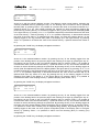
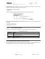
The Fine Gain Value and the Pole Zero can be %0 to %FF. The Status Register Word encodes on 7
bits the Coarse Gain Value, the Shape, the Output Polarity and the Output Configuration as shown in
Fig. 4.1.
15 14 13 12 11 10 9
8
7
6
5
4
3
OP OC SHAPE
2
1
0
COARSE
COARSE GAIN VALUE
SHAPE
OUTPUT CONFIGURATION
OUTPUT POLARITY
Fig. 4.1: Mod. N568B/LC Status Register
Filename:
N568B_N568LC_REV4.DOC
Number of pages:
37
Page:
24
Document type:
User's Manual (MUT)
Title:
Mod. N568B/LC 16 Ch Spectroscopy Amplifiers
Revision date:
26/01/2007
Revision:
4
Operating Code %2; the N568B/LC response to a Read Offset Value is a group of 16 bit words
structured as follows:
- Error Code;
- Offset Value.
Operating Code %3; the N568B/LC response to a Read all Parameters for selected Channel is a
group of 4 words (16 bit) structured as follows:
- Error Code;
- Fine Gain Value selected Channel;
- Pole Zero selected Channel;
- Status Register selected Channel.
Operating Code %4; the N568B/LC response to a Read MUX Enable Status & Last Accessed
Channel is a word (16 bit) structured as follows:
15 14 13 12 11 10 9
8
7
6
5
4
EN
3
2
1
0
CHANNEL N.
Last Accessed Ch.
Not Used
MUX Enable Status (0=Disabled)
(1=Enabled)
Not Used
Operating Codes %10 through %16; the N568B/LC response to any of the 7 Set operations is the
Error Code:
- Error Code.
4.5.1
Error Codes description
The Error Codes provided by the CAENET CAMAC and VME Controllers are described in the
following Table:
Table 4.10: Error Codes (C117B and V288 case)
Datum (Hex)
%0
%FF00
%FF01
%FF02
%FFFD
%FFFE
%FFFF
Meaning
Successful operation.
Module Busy; the Controller has tried to effect an operation while the module is
setting the display brightness.
Code not recognized or message incorrect.
Value out of range.
No data to be transmitted; a start transmission with the Transmit Data Buffer empty
has been attempted (H. S. CAENET Controller error message).
The H.S. CAENET Controller Identifier is incorrect (H. S. CAENET Controller error
message).
The addressed module does not exist. This message is generated after a period of
500 msec (H. S. CAENET Controller error message).
Filename:
N568B_N568LC_REV4.DOC
Number of pages:
37
Page:
25
Document type:
User's Manual (MUT)
4.5.2
Title:
Mod. N568B/LC 16 Ch Spectroscopy Amplifiers
Revision date:
26/01/2007
Revision:
4
Module Identifier Packet (response to code %0)
The response contains in the low byte the ASCII code of the string of characters identified by the
name of the Module plus the version of the software running on the Main Controller.
Table 4.11: Module Identifier Data Packet Structure
Word
4.6
Contents
bits 15..8
bits 7..0
2
0
"N"
3
0
"5"
4
0
"6"
5
0
"8"
6
0
""
7
0
"V"
8
0
"e"
9
0
"r"
10
0
"s"
11
0
"i"
12
0
"o"
13
0
"n"
14
0
""
15
0
"x"
16
0
"."
17
0
"x"
USING THE H. S. CAENET PC CONTROLLERS
The Mod. N568B/LC can be controlled remotely via a standard PC through the Mod. A303, A303A
and A1303 H. S. CAENET PC Controllers.
The Mod. A303 is an 8-bit interface board that can be directly inserted into a std. I/O PC 8-bit slot and
it is mapped in the MS-DOS I/O or memory address space. Therefore it is controllable by all the
languages (high level or assembly), independently from the processor type.
Dip switches located on the printed circuit board allow the User to set the unit according to the
computer to be used (for more information see the Mod. A303 Technical Information Manual).
The board interfaces directly the 8-bit bus with the two FIFO buffers (TX and RX FIFO), and with 6
internal registers that are used for various functions such as the FIFO clearing, the start transmission
and the readout of the Node status.
The Host processor can control the Node operation in polling mode or using the interrupt facility.
Filename:
N568B_N568LC_REV4.DOC
Number of pages:
37
Page:
26
Document type:
User's Manual (MUT)
Title:
Mod. N568B/LC 16 Ch Spectroscopy Amplifiers
Revision date:
26/01/2007
Revision:
4
Due to the 8-bit board, in the case of the A303 PC Controller, Operating Codes and Slave responses
are coded as 8-bit Bytes.
The Mod. A303A HIGH SPEED (H.S.) CAENET CONTROLLER is an ISA interface card. It allows
the control of an H.S. CAENET network through a standard PC.
The card can be mapped either in the I/O or Memory space of the PC (dip switch selectable).
Moreover the Mod. A 303A Controller can operate either in Polling or Interrupt mode (dip switch
selectable).
The communication line uses a simple 50 Ω coaxial cable as its physical transmission medium.
The Mod. A1303 PCI CAENET CONTROLLER is a 32-bit PCI interface card. It allows the control of a
HS CAENET network through a standard PC.
The communication line uses a 50 Ω coaxial cable as its physical transmission medium.
Table 4.12: HS CAENET PC CONTROLLERS registers
Register/Buffer
TX FIFO
Address
Base Ad. + 0
Operation
write
START TX
Base Ad. + 1
write
RESET
Base Ad. + 3
write
RX FIFO
Base Ad. + 0
read
STATUS REGISTER
RESET INTERRUPT
Base Ad. + 1
Base Ad. + 2
read
read
CLEAR RX FIFO
Base Ad. + 3
read
4.7
DESCRIPTION
TX FIFO (512 byte max. depth)
Transmit Data Buffer.
Starts the transmission of the TX FIFO
data
Clears TX and RX buffers and resets
all the Interrupt signals.
RX FIFO (512 byte max. depth)
Receive Data Buffer.
8-bit Status register.
Reads the Status register and clears a
present interrupt.
Clears the RX FIFO
BOARD CONTROL VIA OPC SERVER
CAEN, in close collaboration with CERN (IT/CO group), has developed an OPC server which allows
powerful, flexible, and yet simple control of its modules, indifferently through H.S. CAENET
communication path, by any OPC compliant client application.
Version 2.4 and later of CAEN HV OPC Server are fully compliant with the OPC Data Access 2.0
specifications. The A303A and the A1303 HS CAENET controllers allow to control the N568B and
N568LC via OPC server, through a complete set of programmable/monitorable items, which are
described in the following subsections. Anyway, for an extensive description, the CAEN OPC Server
User’s Manual is available too.
4.7.1
N568B / N568LC board control
This chapter describes the Items which are available for the control of the N568B / N568LC module.
A read access to the ModelName item returns a string with the board model.
A read access to the SwRelease item returns a string with the board software release.
A read access to the CnetCrNum item returns the board Caenet crate number.
A read access to the Slots item returns the number of the board’s slots (1).
Filename:
N568B_N568LC_REV4.DOC
Number of pages:
37
Page:
27
Document type:
User's Manual (MUT)
Title:
Mod. N568B/LC 16 Ch Spectroscopy Amplifiers
Revision date:
26/01/2007
Revision:
4
A read access to the Model item returns a string with the board’s name.
A read access to the Description item returns a string with the board synthetic description.
A read access to the FmwRelease item returns a string with the board firmware release.
A read access to the SerNum item returns a string with the board serial number.
A read access to the NrOfCh item returns the number of board’s channels.
The MuxOut item allows to enable the Multiplexed Output; see the board’s User’s manual for further
details.
A read access to the MuxOut#CoClose item returns back the label “Enable” associated to
Multiplexed Output Enabled.
A read access to the MuxOut#CoOpen item returns back the label “Disable” associated to
Multiplexed Output Disabled.
The LastCh item returns the Latest Channel accessed; see the board’s User’s manual for further
details.
A read access to the LastCh#EU item returns a string with the Latest Channel Engineering Units.
A read access to the LastCh#HighEU item returns the highest possible Latest Channel value.
A read access to the LastCh#LowEU item returns the lowest possible Latest Channel value.
The Offset item allows to set the Offset; see the board’s User’s manual for further details.
A read access to the Offset#EU item returns a string with the Offset Engineering Units.
A read access to the Offset#HighEU item returns the highest possible Offset value.
A read access to the Offset#LowEU item returns the lowest possible Offset value.
Table 4.13– N568B / N568LC Board Items
ItemID
Data Type
Access Rights
Description
N568B.ModelName
String
R
Board model
N568B.SwRelease
String
R
Board software release
N568B.CnetCrNum
2 byte integer
R
Caenet crate number
N568B.Slots
2 byte integer
R
Number of slots
N568B.BoardXX.Model
String
R
Board name
N568B.BoardXX.Description
String
R
Synthetic description
N568B.BoardXX.FmwRelease
String
R
Board firmware release
N568B.BoardXX.SerNum
String
R
Board serial number
N568B.BoardXX.NrOfCh
2 byte integer
R
Number of board channels
Filename:
N568B_N568LC_REV4.DOC
Number of pages:
37
Page:
28
Document type:
User's Manual (MUT)
Title:
Mod. N568B/LC 16 Ch Spectroscopy Amplifiers
Revision date:
26/01/2007
N568B.BoardXX.MuxOut
Boolean
R/W
Enable Multiplexed Output
N568B.BoardXX.MuxOut#CoClose
String
R
Multiplexed Out close label
N568B.BoardXX.MuxOut#CoOpen
String
R
Multiplexed Out open label
N568B.BoardXX.Last
4 byte integer
R/W
Latest channel value
N568B.BoardXX.Last#EU
String
R
Latest ch. EU
N568B.BoardXX.Last#HighEU
8 byte integer
R
Latest ch. upper limit
N568B.BoardXX.Last#LowEU
8 byte integer
R
Latest ch. lower limit
N568B.BoardXX.Offset
4 byte integer
R/W
Offset value
N568B.BoardXX.Offset#EU
String
R
Offset EU
N568B.BoardXX.Offset#HighEU
8 byte integer
R
Offset upper limit
N568B.BoardXX.Offset#LowEU
8 byte integer
R
Offset lower limit
4.7.2
Revision:
4
N568B / N568LC channel control
This chapter describes the Items which are available for the control of a N568B / N568LC channel.
The Name item allows to assign to the channel a symbolic name.
The FineGain item allows to set Fine Gain; see the board User’s manual for details.
A read access to the FineGain#EU item returns a string with the Fine Gain Engineering Units.
A read access to the FineGain#HighEU item returns the highest possible Fine Gain value.
A read access to the FineGain#LowEU item returns the lowest possible Fine Gain value.
The CoarGain item allows to set Coarse Gain; see the board User’s manual for further details.
A read access to the CoarGain#EU item returns a string with the Coarse Gain Engineering Units.
A read access to the CoarGain#HighEU item returns the highest possible Coarse Gain value.
A read access to the CoarGain#LowEU item returns the lowest possible Coarse Gain value.
The PoleZAdj item allows the Pole Zero Adjustment; see the board User’s manual for further details.
A read access to the PoleZAdj#EU item returns a string with the Pole Zero Adjustment Engineering
Units.
A read access to the PoleZAdj#HighEU item returns the highest possible Pole Zero Adjustment
value.
A read access to the PoleZAdj#LowEU item returns the lowest possible Pole Zero Adjustment value.
The Shape item allows the Shape setting; see the board User’s manual for further details.
A read access to the Shape#EU item returns a string with the Shape Engineering Units.
Filename:
N568B_N568LC_REV4.DOC
Number of pages:
37
Page:
29
Document type:
User's Manual (MUT)
Title:
Mod. N568B/LC 16 Ch Spectroscopy Amplifiers
Revision date:
26/01/2007
Revision:
4
A read access to the Shape#HighEU item returns the highest possible Shape value.
A read access to the Shape#LowEU item returns the lowest possible Shape value.
The OutPol item allows to set the Output Polarity; see the board User’s manual for further details.
A read access to the OutPol#CoClose item returns back the label “Negative” associated to Negative
output polarity.
A read access to the OutPol#CoOpen item returns back the label “Positive” associated to to Positive
output polarity.
The OutConf item allows to set the Output Configuration; see the board User’s manual for further
details.
A read access to the OutConf#CoClose item returns back the label “Inverted” associated to Inverted
output.
A read access to the OutConf#CoOpen item returns back the label “Direct” associated to Direct
output.
Filename:
N568B_N568LC_REV4.DOC
Number of pages:
37
Page:
30
Document type:
User's Manual (MUT)
Title:
Mod. N568B/LC 16 Ch Spectroscopy Amplifiers
Revision date:
26/01/2007
Revision:
4
Table 4.14– N568B / N58LC Channel items
ItemID
Data Type
Access Rights
Description
N568B.BoardXX.ChanYYY.Name
String
R/W
Channel name
N568B.BoardXX.ChanYYY.FineGain
4 byte integer
R/W
Set Fine Gain
N568B.BoardXX.ChanYYY. FineGain#EU
String
R
Fine Gain EU
N568B.BoardXX.ChanYYY. FineGain#HighEU
8 byte integer
R
Fine Gain upper limit
N568B.BoardXX.ChanYYY. FineGaint#LowEU
8 byte integer
R
Fine Gain lower limit
N568B.BoardXX.ChanYYY.CoarGain
4 byte integer
R/W
Set Coarse Gain
N568B.BoardXX.ChanYYY.CoarGain#EU
String
R
Coarse Gain EU
N568B.BoardXX.ChanYYY.CoarGain#HighEU
8 byte integer
R
Coarse Gain upper limit
N568B.BoardXX.ChanYYY.CoarGain#LowEU
8 byte integer
R
Coarse Gain lower limit
N568B.BoardXX.ChanYYY.PoleZAdj
4 byte integer
R/W
Allows Pole Zero Adjustment
N568B.BoardXX.ChanYYY.PoleZAdj#EU
String
R
Pole Zero Adjustment EU
N568B.BoardXX.ChanYYY.PoleZAdj#HighEU
8 byte integer
R
Pole Zero Adj. upper limit
N568B.BoardXX.ChanYYY.PoleZAdj#LowEU
8 byte integer
R
Pole Zero Adj. lower limit
N568B.BoardXX.ChanYYY.Shape
4 byte integer
R/W
Set Shape
N568B.BoardXX.ChanYYY.Shape#EU
String
R
Shape EU
N568B.BoardXX.ChanYYY.Shape#HighEU
8 byte integer
R
Shape upper limit
N568B.BoardXX.ChanYYY.Shape#LowEU
8 byte integer
R
Shape lower limit
N568B.BoardXX.ChanYYY.OutPol
Boolean
R/W
Set Output Polarity
N568B.BoardXX.ChanYYY.OutPol#CoClose
String
R
Out polarity close label
N568B.BoardXX.ChanYYY.OutPol#CoOpen
String
R
Out polarity open label
N568B.BoardXX.ChanYYY.OutConf
Boolean
R/W
Set Output Configuration
N568B.BoardXX.ChanYYY.OutConf#CoClose
String
R
Out configuration close label
N568B.BoardXX.ChanYYY.OutConf#CoOpen
String
R
Out configuration open label
4.8
4.8.1
DATA COMPOSITION (PC CONTROLLER CASE)
Master to Slave Data Composition (PC Controller Case)
The MASTER-to-SLAVE data have to be written into the Transmit Data buffer by performing
subsequent write operations as described in the table below:
Filename:
N568B_N568LC_REV4.DOC
Number of pages:
37
Page:
31
Document type:
User's Manual (MUT)
Title:
Mod. N568B/LC 16 Ch Spectroscopy Amplifiers
Revision date:
26/01/2007
Revision:
4
Table 4.15: Master to Slave data composition
Order
1
2
3
4
4.8.2
Operation
Address
Datum (HEX)
Meaning
write
Base Ad. + 0
low byte = %01
H.S.
write
Base Ad. + 0
high byte = %00
identified code
write
Base Ad. + 0
low byte = %XX
write
Base Ad. + 0
high byte = %00
write
Base Ad. + 0
low byte Code
First 2 Bytes of the Operation
write
Base Ad. + 0
high byte Code
Code to be performed
write
Base Ad. + 0
low byte Code/Set
write
Base Ad. + 0
high byte Code/Set
CAENET
Controller
Module Number
Possible 2 Bytes of the Set value
Slave to Master Data Composition (PC Controller Case)
The answer data coming from the N568B/LC are automatically stored into the HS CAENET controller
Receive Data buffer and therefore are available to the User.
The following Table shows the structure of the N568B/LC data packet:
Table 4.16: Slave to Master data composition
Order
Operation
Address
Datum
Meaning
read
Base Ad. + 0
read
Base Ad. + 0
low byte = %01
high byte = %00
H.
S.
CAENET
identified code
read
Base Ad. + 0
Error code
read
Base Ad. + 0
low byte Error code
high byte Error code
read
Base Ad. + 0
low byte value
read
Base Ad. + 0
high byte value
1
2
3 to 100(*)
4.9
Controller
Possible Parameter value
MASTER TO SLAVE OPERATING CODES (PC CONTROLLER
CASE)
The MASTER-to-SLAVE Operating Codes of the module N568B/LC have the following structure:
-
Byte 1: %01 (Low Byte Controller identified code);
Byte 2: %00 (High Byte Controller identified code);
Byte 3: %XX (Low Byte Module Number);
Byte 4: %00;
Byte 5 ÷ 8: see Table 4.17
Filename:
N568B_N568LC_REV4.DOC
Number of pages:
37
Page:
32
Document type:
User's Manual (MUT)
Title:
Mod. N568B/LC 16 Ch Spectroscopy Amplifiers
Revision date:
26/01/2007
Revision:
4
Table 4.17: Operating Codes of the N568B/LC
Byte 5 (Hex)
Byte 6*
Byte 7** Byte 8 Meaning
%0
0
==
==
Module identifier
%1
0
==
==
Read all Parameters for all Channels + Offset Value
%2
0
==
==
Read Offset Value
%3
%n
==
==
Read all Parameters for Channel n
%4
0
==
==
Read MUX Enable Status & Last Accessed Channel
%10
%n
%m
0
Set Channel n Fine Gain
%11
%n
%p
0
Set Channel n Coarse Gain
%12
%n
%m
0
Set Channel n Pole Zero Adjustment
%13
%n
%q
0
Set Channel n Shape
%14
%n
%b
0
Set Channel n Output Polarity
%15
%n
%b
0
Set Channel n Output Configuration
%16
0
%m
0
Set Offset Value
%20
0
==
==
Disable Multiplexed Outputs
%21
0
==
==
Enable Multiplexed Outputs
*) n is the Channel Number (%0 to %F for a selected channel, %10 for a set/read in common to all
Channels);
**) allowed values (HEX):
m=0 to FF;
p=0 to 7;
q=0 to 3;
b=0 to 1;
4.10 SET VALUES
Operating Code %10; the allowed Fine Gain values are %0 to %FF, corresponding approximately to
a multiplying factor from 0.2 (%0) to 2 (%FF) to be applied to the Coarse Gain value.
Operating Code %11; the allowed Coarse Gain values for each Channel are 0 to 7: each step
corresponds approximately to a doubling of the Coarse Gain value. Due to the dependence of the
Gain value from the Shaping Times and Input Signal Risetimes, it is meaningless to quote an absolute
Gain value setting (see §3.2.5). As an example, if the measured amplifier Gain (@ Coarse Set value
0, Fine Set value 0, Shaping time 0.2 μs and Input Signals Rise Time 0.2 μs) is 1, it will be 16 at set
value 4 with the same configuration on the other settings. Relative set Values are given as follows:
Filename:
N568B_N568LC_REV4.DOC
Number of pages:
37
Page:
33
Document type:
User's Manual (MUT)
Title:
Mod. N568B/LC 16 Ch Spectroscopy Amplifiers
Revision date:
26/01/2007
Revision:
4
Table 4.18: Coarse Gain Values
Code %11
Set
Relative Coarse Gain
Value (approx.)
%0
%1
%2
%3
%4
%5
%6
%7
1
2
4
8
16
32
64
128
Operating Code %12; the allowed Pole Zero values for each Channel are %0 to %FF, allowing to
match the preamplifier tails in a range 50-500 μs.
Operating Code %13; the allowed Shape values for each Channel are %0 to %3, corresponding to
the Shaping Time Values as follows:
Table 4.19: Shape Values
Code %13
Set
Shape
Value
%0
%1
%2
%3
0.2 μs
1 μs
3 μs
6 μs
Operating Code %14; the allowed Output Polarity values for each Channel are 0 or 1, corresponding
respectively to Positive (0) or Negative (1) Output Polarity.
Operating Code %15; the allowed Output Configuration values for each Channel are 0 or 1,
corresponding respectively to Direct (0) or Inverted (1) Outputs.
Operating Code %16; the allowed Offset value in common to all Channels is %0 to %FF.
4.11 SLAVE TO MASTER DATA PACKET DESCRIPTION (PC
CONTROLLER CASE)
The answer data coming from the Mod. N568B/LC or from the H. S. CAENET CAMAC or VME
Controllers are different according to the different Operating Codes performed.
Operating Code %0; the N568B/LC response to a Module Identifier Operation is a group of 8 bit
Bytes structured as follows:
- %01 (Low Byte of Master Identifier Code);
- %00 (High Byte of Master Identifier Code);
- Low Byte of the Error Code;
Filename:
N568B_N568LC_REV4.DOC
Number of pages:
37
Page:
34
Document type:
User's Manual (MUT)
Title:
Mod. N568B/LC 16 Ch Spectroscopy Amplifiers
Revision date:
26/01/2007
Revision:
4
- High Byte of the Error Code;
- Low Byte of the Module Identifier's first word;
- High Byte of the Module Identifier's first word;
...
...
- Low Byte of the Module Identifier's sixteenth word;
- High Byte of the Module Identifier's sixteenth word.
Operating Code %1; the N568B/LC response to a Read Module Configuration is a group of 8 bit
Bytes structured as follows:
- %01 (Low Byte of Master Identifier Code);
- %00 (High Byte of Master Identifier Code);
- Low Byte of the Error Code;
- High Byte of the Error Code;
- Low Byte of the Fine Gain Value word CH. 0;
- High Byte of the Fine Gain Value word CH. 0;
- Low Byte of the Pole Zero word CH. 0;
- High Byte of the Pole Zero word CH. 0;
- Low Byte of the Status Register word CH. 0;
- High Byte of the Status Register word CH. 0;
- Low Byte of the Fine Gain Value word CH. 1;
....
....
- High Byte of the Status Register word CH. 15;
- Low Byte of the Offset Value word;
- High Byte of the Offset Value word.
The Fine Gain Value and the Pole Zero can be %0 to %FF. The Status Register Word encodes on 7
bits the Coarse Gain Value, the Shape, the Output Polarity and the Output Configuration as shown in
Fig. 4.1.
Operating Code %2; the N568B/LC response to a Read Offset Value is a group of 8 bit Bytes
structured as follows:
- Low Byte of the Error Code;
- High Byte of the Error Code;
- Low Byte of the Offset Value word;
- High Byte of the Offset Value word.
Operating Code %3; the N568B/LC response to a Read all Parameters for selected Channel is a
group of 8 bit Bytes structured as follows:
-
Low Byte of the Error Code;
High Byte of the Error Code;
Low Byte of the Fine Gain Value selected Channel;
High Byte of the Fine Gain Value selected Channel;
Low Byte of the Pole Zero selected Channel;
High Byte of the Pole Zero selected Channel;
Low Byte of the Status Register selected Channel;
High Byte of the Status Register selected Channel.
Filename:
N568B_N568LC_REV4.DOC
Number of pages:
37
Page:
35
Document type:
User's Manual (MUT)
Title:
Mod. N568B/LC 16 Ch Spectroscopy Amplifiers
Revision date:
26/01/2007
Revision:
4
Operating Code %4; the N568B/LC response to a Read MUX Enable Status & Last Accessed
Channel is composed by 2 8-bit bytes structured as follows:
- Channel Number and MUX enable bit;
- Blank byte;
The byte containing Channel Number and MUX enable bit is structured as follows:
7
6
5
EN
4
3
2
1
0
CHANNEL N.
Last Accessed Ch.
Not Used
MUX Enable Status (0=Disabled)
(1=Enabled)
Operating Codes %10 through %16; the N568B/LC response to any of the 7 Set operations is the
Error Code:
- Low Byte of the Error Code;
- High Byte of the Error Code.
4.11.1
Error Codes description
The Error Codes provided by the CAENET controllers are described in the following Table:
Table 4.20: Error Codes
Datum (Hex)
%0
%FF00
%FF01
%FF02
Meaning
Successful operation.
Module Busy; the Controller has tried to effect an operation while the module is
setting the display brightness.
Code not recognized or message incorrect.
Value out of range.
4.11.2 Module Identifier Packet (response to code %0)
The response contains in the low byte the ASCII code of the string of characters identified by the
name of the Module plus the version of the software running on the Main Controller.
Filename:
N568B_N568LC_REV4.DOC
Number of pages:
37
Page:
36
Document type:
User's Manual (MUT)
Title:
Mod. N568B/LC 16 Ch Spectroscopy Amplifiers
Revision date:
26/01/2007
Revision:
4
Table 4.21: Module Identifier Data Packet Structure
Word
Contents
High byte 15..8
Low byte
7..0
2
0
"N"
3
0
"5"
4
0
"6"
5
0
"8"
6
0
""
7
0
"V"
8
0
"e"
9
0
"r"
10
0
"s"
11
0
"i"
12
0
"o"
13
0
"n"
14
0
""
15
0
"x"
16
0
"."
17
0
"x"
Filename:
N568B_N568LC_REV4.DOC
Number of pages:
37
Page:
37