1
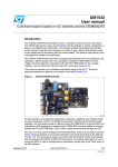
UM1482
User Manual
STM8SVLDISCOVERY
STM8S value line discovery
Introduction
The STM8SVLDISCOVERY is a quick start evaluation kit which helps you to discover the
STM8S value line features, and to develop your own application. It is based on an
STM8S003 and includes an embedded debugger, ST-LINK, and a user button. Numerous
applications are available from www.st.com/stm8svldiscovery.
Features
●
STM8S003K3T6 microcontroller, 8 KB Flash, 1 KB RAM, 128 bytes EEPROM
●
Powered by USB cable between PC and STM8SVLDISCOVERY
●
Selectable power of 5 V or 3.3 V
●
Push button, B1
●
User LED, LD1
●
Extension header for all I/Os
●
Wrapping area for users own application
●
Embedded ST-LINK for STM8S
●
USB interface for programming and debugging
●
SWIM debug support
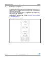
Figure 1.
November 2011
STM8SVLDISCOVERY evaluation board
Doc ID 022392 Rev 1
1/20
www.st.com
Contents
UM1482
Contents
1
Quick start . . . . . . . . . . . . . . . . . . . . . . . . . . . . . . . . . . . . . . . . . . . . . . . . . 5
2
Hardware and layout . . . . . . . . . . . . . . . . . . . . . . . . . . . . . . . . . . . . . . . . . 6
2.1
STM8S003K3T6 microcontroller . . . . . . . . . . . . . . . . . . . . . . . . . . . . . . . . 8
2.2
ST-LINK . . . . . . . . . . . . . . . . . . . . . . . . . . . . . . . . . . . . . . . . . . . . . . . . . . 10
2.2.1
Using the ST-LINK . . . . . . . . . . . . . . . . . . . . . . . . . . . . . . . . . . . . . . . . . 10
2.2.2
Using the ST-LINK on other STM8S applications . . . . . . . . . . . . . . . . . 10
2.3
Power supply and power selection . . . . . . . . . . . . . . . . . . . . . . . . . . . . . . 12
2.4
LEDs . . . . . . . . . . . . . . . . . . . . . . . . . . . . . . . . . . . . . . . . . . . . . . . . . . . . 12
2.5
Push button . . . . . . . . . . . . . . . . . . . . . . . . . . . . . . . . . . . . . . . . . . . . . . . 12
3
Daughterboard connection . . . . . . . . . . . . . . . . . . . . . . . . . . . . . . . . . . 13
4
Mechanical drawing . . . . . . . . . . . . . . . . . . . . . . . . . . . . . . . . . . . . . . . . 15
5
Electrical schematics . . . . . . . . . . . . . . . . . . . . . . . . . . . . . . . . . . . . . . . 16
6
Revision history . . . . . . . . . . . . . . . . . . . . . . . . . . . . . . . . . . . . . . . . . . . 19
2/20
Doc ID 022392 Rev 1
UM1482
List of tables
List of tables
Table 1.
Table 2.
Table 3.
Table 4.
Table 5.
Table 6.
SWIM connector CN7 . . . . . . . . . . . . . . . . . . . . . . . . . . . . . . . . . . . . . . . . . . . . . . . . . . . . . 11
CN1 pinout . . . . . . . . . . . . . . . . . . . . . . . . . . . . . . . . . . . . . . . . . . . . . . . . . . . . . . . . . . . . . 13
CN2 pinout . . . . . . . . . . . . . . . . . . . . . . . . . . . . . . . . . . . . . . . . . . . . . . . . . . . . . . . . . . . . . 13
CN3 pinout . . . . . . . . . . . . . . . . . . . . . . . . . . . . . . . . . . . . . . . . . . . . . . . . . . . . . . . . . . . . . 14
CN4 pinout . . . . . . . . . . . . . . . . . . . . . . . . . . . . . . . . . . . . . . . . . . . . . . . . . . . . . . . . . . . . . 14
Document revision history . . . . . . . . . . . . . . . . . . . . . . . . . . . . . . . . . . . . . . . . . . . . . . . . . 19
Doc ID 022392 Rev 1
3/20
List of figures
UM1482
List of figures
Figure 1.
Figure 2.
Figure 3.
Figure 4.
Figure 5.
Figure 6.
Figure 7.
Figure 8.
Figure 9.
Figure 10.
Figure 11.
Figure 12.
Figure 13.
4/20
STM8SVLDISCOVERY evaluation board. . . . . . . . . . . . . . . . . . . . . . . . . . . . . . . . . . . . . . . 1
Hardware block diagram . . . . . . . . . . . . . . . . . . . . . . . . . . . . . . . . . . . . . . . . . . . . . . . . . . . . 6
Top layout . . . . . . . . . . . . . . . . . . . . . . . . . . . . . . . . . . . . . . . . . . . . . . . . . . . . . . . . . . . . . . 7
STM8S003K3T6 package. . . . . . . . . . . . . . . . . . . . . . . . . . . . . . . . . . . . . . . . . . . . . . . . . . . 8
STM8S003 block diagram . . . . . . . . . . . . . . . . . . . . . . . . . . . . . . . . . . . . . . . . . . . . . . . . . . 9
Typical configuration . . . . . . . . . . . . . . . . . . . . . . . . . . . . . . . . . . . . . . . . . . . . . . . . . . . . . . 10
ST-LINK without breaking the PCB . . . . . . . . . . . . . . . . . . . . . . . . . . . . . . . . . . . . . . . . . . 10
Separated ST-LINK module . . . . . . . . . . . . . . . . . . . . . . . . . . . . . . . . . . . . . . . . . . . . . . . . 11
Power selection . . . . . . . . . . . . . . . . . . . . . . . . . . . . . . . . . . . . . . . . . . . . . . . . . . . . . . . . . 12
STM8SVLDISCOVERY mechanical drawing . . . . . . . . . . . . . . . . . . . . . . . . . . . . . . . . . . . 15
STM8SVLDISCOVERY . . . . . . . . . . . . . . . . . . . . . . . . . . . . . . . . . . . . . . . . . . . . . . . . . . . 16
STM8SVLDISCOVERY MCU . . . . . . . . . . . . . . . . . . . . . . . . . . . . . . . . . . . . . . . . . . . . . . . 17
STM8SVLDISCOVERY ST-LINK (SWIM only). . . . . . . . . . . . . . . . . . . . . . . . . . . . . . . . . . 18
Doc ID 022392 Rev 1
UM1482
1
Quick start
Quick start
It is very simple to get started using the STM8SVLDISCOVERY, just follow these four steps:
1.
Connect the STM8SVLDISCOVERY to a PC with a USB cable.
2.
Press the B1 button, and observe LED LD1 blinking.
3.
Press the B1 button to change blinking speed.
4.
Visit www.st.com/stm8svldiscovery and follow the tutorial, then discover other
applications.
You can discover more of the STM8S features by downloading and executing the proposed
programs in the project list.
Note:
The software code corresponding to this application is available under the name Discover
(AN3996) in the project list of the STM8SVLDISCOVERY web page.
Doc ID 022392 Rev 1
5/20
Hardware and layout
2
UM1482
Hardware and layout
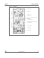
The STM8SVLDISCOVERY is designed around the STM8S003K3T6 microcontroller in an
LQFP32 package. It has two distinct sections that may be separated, the STM8S003K3T6
module and the ST-LINK module.
Figure 2 illustrates the connections between the STM8S003K3T6 and its peripherals (STLINK, user button, LED and connectors).
Figure 3 helps you to locate these features on the STM8SVLDISCOVERY board, as well as
the potential point of separation (for more details refer to Section 2.2.2: Using the ST-LINK
on other STM8S applications).
Figure 2.
6/20
Hardware block diagram
Doc ID 022392 Rev 1
UM1482
Hardware and layout
Figure 3.
Top layout
USB connector
CN5
MB1008A
LD2
R15
R21
R18
R22
C17
C19
LED (LD2 )
1
CN6
C18
U4
C16
U2
C13
C12
ST-LINK core
R9
R14
R8
R13
X2
R12
ST-LINK module
R17
SWIM connector
R19
C11
R16
CN7
R20
C15
C14
SB1
SB2
www.st.com/stm8svldiscovery
PD2
PD0
JP1
PD4
CN4
1
C9
C10
PD1
PC7
PC5
PC3
PC1
RoHS
PC6
PC4
PC2
PE5
C1
R7
External oscillator (16 MHz) footprint
R5
STM8S003K3T6
CN2
X1
R100
PB0
PB2
C8
PB4
C4
PB6
SB5
1
C100
C5
CN3
User button (B1)
PB1
PB3
1
PB5
NRST PA1
PA2 GND
GND VCAP
PA3 PF4
PB7
STM8S003K3T6 module
PD3
U1
PD5
CN1
PD7
C3
1
LED (LD1)
Power supply jumper
R1
LD1
3V3 VDD U5V
PD6
1
Possible separation point
STM8S Value line discovery
B1
Wrapping area
U3
SO16 footprint
Doc ID 022392 Rev 1
7/20
Hardware and layout
2.1
UM1482
STM8S003K3T6 microcontroller
Figure 4.
STM8S003K3T6 package
4HE34-3+4BITMICROCONTROLLEROFFERS
+BYTESOF&LASHPROGRAMMEMORY
BYTESDATA%%02/+BYTE2!,1&0X
-36
This device provides the following key features:
●
High-performance proprietary 8-bit core with excellent code density
●
Innovative design architecture, 16-bit index registers, 32-bit memory interface and 3stage pipeline
●
Leading-edge embedded Flash memory technology
●
Advanced clock controller to optimize power consumption and noise control
●
Large set of embedded peripherals: UART, I²C, SPI, timers, analog, and debugging
function
These features provide the following benefits:
●
Cost efficiency based on optimized product manufacturing flow
●
Lower system cost with embedded peripherals
●
Full compatibility with existing STM8S product portfolio
●
Efficient power management
●
Easy-to-use, non-intrusive, and low-cost development environment
It is particularly suitable for applications such as:
8/20
●
Consumer electronics
●
Large-volume industrial equipment
●
PC peripherals
●
All mass market electronics
Doc ID 022392 Rev 1
UM1482
Hardware and layout
Figure 5.
STM8S003 block diagram
'%
%%%
'
'
")
*)
%&&+$%'$,
,. /
!,&, /
2330'
'
!-($'
"!(%
01
&$(
7%$'+
!
! "!
,,''$,,$$'
%.
,4
1
,$$<<")
01
$,8$,
%(9!
:
#
$%&&'
(9!
:
#&;
+$%'
2
&
*&
$'(
9!
2:
#&
2")
+$%'56
(&%($1
&'
#&
6")
+$%'
#(
For more information see the STM8S003xx datasheet (Doc ID 018576) on the ST website.
Doc ID 022392 Rev 1
9/20
Hardware and layout
2.2
UM1482
ST-LINK
The ST-LINK provides a USB interface for programming and debugging using a single wire
interface module (SWIM). The ST-LINK module of the STM8SVLDISCOVERY also supplies
5 V and 3.3 V to the STM8S003K3T6 module.
2.2.1
Using the ST-LINK
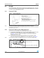
Figure 6.
Typical configuration
(ARDWAREREQUIREMENTS
53"CABLETYPE!TO"
#OMPUTERWITH7INDOWS806ISTAOR
/PTIONALSOFTWAREENVIRONMENT
)!2%MBEDDED7ORKBENCHFOR34-
344OOLSET346ISUAL$EVELOPAND346ISUAL0ROGRAM
WHICHSUPPOR T34,).+37)-
.OTE346$REQUIRES#OSMICOR2AISONANCE #OMPILER
-36
Note:
The driver for ST-LINK is installed automatically when the USB is connected.
For information about debugging and programming features refer to ST-LINK, STVD, STVP
and SWIM on www.st.com.
2.2.2
Using the ST-LINK on other STM8S applications
You can connect your ST-LINK to other STM8S applications in 2 ways:
Note:
●
By removing the solder bridges: This way uses the ST-LINK without breaking the PCB.
Unsolder the two solder bridges SB1 and SB2 under the SWIM connector.
See Figure 7. You can re-solder the two bridges at a later date thus keeping the
STM8SVLDISCOVERY usable.
●
By breaking the board and removing the ST-LINK: This way constitutes a good
alternative to programming the STM8S devices in other applications. See Figure 8.
This ST-LINK only supports the STM8S family. Do not use it with other STM8 families.
Figure 7.
ST-LINK without breaking the PCB
U2
C13
C12
R9
SWIM connector CN7
R14
R8
R12
R13
X2
SB2
R19
C11
R16
CN7
R20
C15
SB1
C14
www.st.com/stm8svldiscovery
Remove SB1 and SB2 solder bridges
1
10/20
3V3 VDDU5V
LD1
R1
Doc ID 022392 Rev 1
UM1482
Hardware and layout
Figure 8.
Separated ST-LINK module
-;
*33
=
;
-
#2
=
>
#
34-3+4
EVALBOARD
6
>
2
6
*
>
-=
3
;
2
*
...'('('8%,'81
34,).+
37)-CONNECTOR
-36
Warning:
Table 1.
By removing this module you will lose power supply on the
STM8S003K3T6 evaluation board. Consequently, you will
need a SWIM cable and an external power supply to program
and use the STM8S003K3T6 board.
To reconnect your STM8S003K3T6 use connector CN7 see
Table 1.
SWIM connector CN7
Pin
CN2
Designation
1
VDD_TARGET
VDD from application
2
SWIM
SWIM data input/output
3
GND
Ground
4
SWIM_RST
SWIM reset
Doc ID 022392 Rev 1
11/20
Hardware and layout
2.3
UM1482
Power supply and power selection
The power supply is provided by a USB connector. Jumper JP1 selects the VDD value (5 V
or regulated 3.3 V) see Figure 9.
Figure 9.
2.4
Power selection
LEDs
The ST-LINK provides two LEDs:
2.5
●
LD1: Green LED LD1 is connected to the I/O PD0 of STM8S003K3.
●
LD2: Red LED LD2 indicates communication between PC and ST-LINK.
Push button
Push button B1 is connected to the I/O PB7 of STM8S003K3.
12/20
Doc ID 022392 Rev 1
UM1482
Daughterboard connection
Four 12-pin male headers CN1, CN2, CN3 and CN4 are connected to the STM8S003K3T6
microcontroller.
See the following tables for pin assignments.
CN1 pinout
CN1 Pin
pin (chip)
Pin name
Type
Table 2.
Main function
1
1
NRST
I/O
Reset
2
2
OSCIN/PA1
I/O
Port A1
3
3
OSCOUT/PA2 I/O
Port A2
4
4
GND
S
Digital ground
5
4
GND
S
Digital ground
6
5
VCAP
S
1.8 V regulator
capacitor
NC
6
VDD
S
Digital power supply
7
7
PA3
I/O
Port A3
8
8
PF4
I/O
Port F4
Table 3.
CN2 Pin
pin (chip)
Alternate function
Timer 2 - channel 3 / SPI master slave
CN2 pinout
Pin name
Type
3
Daughterboard connection
Main function
Alternate function
1
17
PE5
I/O Port E5
SPI master slave
2
18
PC1
I/O Port C1
Timer 1 - channel 1 /
UART2 synchronous clock
3
19
PC2
I/O Port C2
Timer 1 - channel 2
4
20
PC3
I/O Port C3
Timer 1 - channel 3
5
21
PC4
I/O Port C4
Timer 1 - channel 4
6
22
PC5
I/O Port C5
SPI clock
7
23
PC6
I/O Port C6
SPI master out / slave in
8
24
PC7
I/O Port C7
SPI master in / slave out
Doc ID 022392 Rev 1
13/20
Daughterboard connection
CN3 pinout
CN3 Pin
in (chip)
Main function
Alternate function
1
9
PB7/B1
IO
Port B7
2
10
PB6
IO
Port B6
3
11
PB5
I/O Port B5
I2C data
4
12
PB4
I/O Port B4
I2C clock
5
13
PB3
I/O Port B3
Analog input 3 /
Timer 1 external trigger
6
14
PB2
I/O Port B2
Analog input 2 /
Timer 1 inverted channel 3
7
15
PB1
I/O Port B1
Analog input 1 /
Timer 1 inverted channel 2
8
16
PB0
I/O Port B0
Analog input 0 /
Timer 1 inverted channel 1
CN4 Pin
pin (chip)
CN4 pinout
Pin name
Type
Table 5.
14/20
Pin name
Type
Table 4.
UM1482
Main function
Alternate function
1
25
PD0/LD1
I/O Port D0
Timer 1 - break input /
configurable clock output
2
26
PD1/SWIM
I/O Port D1
SWIM data interface
3
27
PD2
I/O Port D2
Timer 2 - channel 3
4
28
PD3
I/O Port D3
Timer 2 - channel 2 /
ADC external trigger
5
29
PD4
I/O Port D4
Timer 2 - channel 1 /
BEEP output
6
30
PD5
I/O Port D5
UART1 data transmit
7
31
PD6
I/O Port D6
UART1 data receive
8
32
PD7
I/O Port D7
Top level interrupt /
Timer 1 - channel 4
Doc ID 022392 Rev 1
UM1482
4
Mechanical drawing
Mechanical drawing
Figure 10. STM8SVLDISCOVERY mechanical drawing
45mm
40.64mm
7.6mm
4.36mm
CN5
LD2
R17
1
R15
R18
U4
R22
CN6
C18
R21
32.98mm
MB1008A
C17
C19
C16
43.18mm
U2
C13
C12
R9
R14
R8
R13
R12
X2
R19
www.st.com/stm8svldiscovery
PD0
PD2
JP1
PD4
CN4
PD1
PD3
U1
PD5
CN1
PD7
1
PC7
PC5
PC3
PC1
RoHS
C3
PC6
PC4
PC2
PE5
C1
R7
CN2
X1
R100
1
C100
C5
7.62mm
CN3
PB1
1
2.54mm
U3
B1
22.86mm
22.86mm
STM8S Value line discovery
15.24mm
PB0
PB2
PB3
C8
PB4
C4
PB5
PA1
GND
VCAP
PF4
PB6
SB5
NRST
PA2
GND
PA3
PB7
15.24mm
R5
15.24mm
1
C9
C10
106.64mm
R1
LD1
3V3 VDDU5V
PD6
1
10.16mm
R20
R16
15.24mm
C14
SB1
SB2
2.54mm
106.64mm
C11
C15
CN7
5.08mm
12.7mm
7.62mm
1.82mm
15.24mm
2.54mm
45mm
Doc ID 022392 Rev 1
15/20
Electrical schematics
Electrical schematics
16/20
5
Figure 11. STM8SVLDISCOVERY
Doc ID 022392 Rev 1
U_ST_LINK
ST_LINK.SCHDOC
RESET#
ST_LINK_SWIM
U_MCU
MCU.SchDoc
SB1
SB2
RESET#
ST_LINK_SWIM
Title:
STM8SVALUE-Discovery
Number:MB1008
Rev: A.1(PCB.SCH)
Date: 7/13/2011
Sheet 1
of
3
UM1482
STMicroelectronics
1
2
3
4
CN1
NRST
PA2
PA3
1
3
5
7
CN2
PA1
2
4
6
8
PE5
PC2
PC4
PC6
VCAP
PF4
1
3
5
7
Header 4X2H
Header 4X2H
Right
1
CN3
PB7
PB5
PB3
PB1
2
LD1
Green
1
3
5
7
CN4
PD0
PD2
PD4
PD6
PB6
PB4
PB2
PB0
2
4
6
8
Header 4X2H
R1
510
1
3
5
7
PD1
PD3
PD5
PD7
2
4
6
8
Header 4X2H Top
Down
VDD
PD7
PD6
PD5
PD4
PD3
PD2
PD1
PD0
Extension connector
32
31
30
29
28
27
26
25
R7
10K
RESET#
C1
10nF
U1
STM8S003K3T6C
PD7
PD6
PD5
PD4
PD3
PD2
PD1
PD0
Doc ID 022392 Rev 1
Not Fitted
PC1
PC3
PC5
PC7
2
4
6
8
Left
VDD
ST_LINK_SWIM
UM1482
Figure 12. STM8SVLDISCOVERY MCU
Not Fitted
NRST
PA1
PA2
C3
20pF
VCAP
X1
16MHz
C4
20pF
R5
PA3
PF4
60
1
2
3
4
5
6
7
8
NRST
OSCIN/PA1
OSCOUT/PA2
Vss
VCAP
Vdd
PA3
PF4
PC7
PC6
PC5
PC4
PC3
PC2
PC1
PE5
VDD
9
10
11
12
13
14
15
16
680nF
VDD
24
23
22
21
20
19
18
17
PB7
PB6
PB5
PB4
PB3
PB2
PB1
PB0
C5
PC7
PC6
PC5
PC4
PC3
PC2
PC1
PE5
U5V
100nF
2
3
2
+3V3
JP1 VDD
3
C8
100nF
C9
100nF
C10
100nF
STMicroelectronics
USER & WAKE-UP Button
Title:
STM8SVALUE-Discovery MCU
17/20
Number:MB1008
1
2
3
Rev: A.1(PCB.SCH)
Date: 7/13/2011
4
Sheet 2
of
3
Electrical schematics
C100
1
SW-PUSH-CMS
B1
SB5
4
1
PB7
PB6
PB5
PB4
PB3
PB2
PB1
PB0
R100
4.7K
PB7
1
2
3
Electrical schematics
18/20
Figure 13. STM8SVLDISCOVERY ST-LINK (SWIM only)
4
R15
VDD
U2
STM32F103C8T6
48
47
46
45
44
43
42
41
40
39
38
37
+3V3
SWIM_IN
SWIM_RST
SWIM_RST_IN
STM_JRST
STM_JTDO
STM_JTDI
STM_JTCK
SWIM_IN
SWIM
100K
2
+3V3
8MHz
R16
100K
VBAT
PC13
PC14
PC15
OSC_IN
OSC_OUT
/RST
VSSA
VDDA
PA0
PA1
U2_TX
Not Fitted
CN5
STM_JRST
STM_JTDI
STM_JTCK
8
6
4
7
5 STM_JTMS
3 STM_JTDO
1
R12
680
R8
SWIM_IN
SWIM_RST_IN R9
+3V3
VDD_2
VSS_2
JTMS
PA12
PA11
PA10
PA9
PA8
S2_MOSI
S2_MISO
S2_CK
PB12
36
35
34
33
32
31
30
29
28
27
26
25
220
220
SWIM
SWIM_RST
ST_LINK_SWIM
RESET#
CN7
1
2
3
4
T_JTMS
T_JTCK
Header 4
SWIM
+3V3
+3V3
MCU
R17
ST_LINK_LED
510
R18
1K5
VCC
DD+
GND
SHELL
SHELL
47
47
VDD
+3V3
VDD
U5V
CN6
R13
R14
STM_JTMS
USB_DP
USB_DM
U1_RX
U1_TX
ST_LINK_LED
JTAG
1
2
3
4
0
0
R21
R22
22 USB_DM
22 USB_DP
U5V
C18
4.7uF
USB-typeB connector
Vin
Vout
RED
R19
R20
4K7
4K7
LED
+3V3
2
C19
4.7uF
C12
104P
C13
104P
C17
104P
STMicroelectronics
C14
104P
2
STM8SVALUE-Discovery ST_LINK (SWIM only)
Number:MB1008
3
Rev: A.1(PCB.SCH)
Date: 7/13/2011
4
Sheet 3
of
3
UM1482
Title:
USB
1
LD2
AIN_1
U4
LD1117-3V3
3
1
Doc ID 022392 Rev 1
1
2
3
4
SWIM_PULLUP_CTL
5
OSC_IN
OSC_OUT 6
STM_RST 7
8
C11
9
100nF+3V3 AIN_1 10
M25_CS 11
U2_TX 12
U2_RX
U2_CK
S1_CK
S1_MISO
S1_MOSI
PB0
PB1
PB2/BOOT1
PB10
PB11
VSS_1
VDD_1
+3V3
VDD_3
VSS_3
PB9
PB8
BOOT0
PB7
PB6
PB5
JNRST
JTDO
JTDI
JTCK
C16
20pF
13
14
15
16
17
18
19
20
SWIM_IN 21
22
SWIM
23
24
1
X2
U2_RX
U2_CK
T_JTCK
T_JTDO
T_JTDI
T_NRST
T_JRST
C15
20pF
UM1482
6
Revision history
Revision history
Table 6.
Date
18-Nov-2011
Document revision history
Revision
1
Changes
Initial release.
Doc ID 022392 Rev 1
19/20
UM1482
Please Read Carefully:
Information in this document is provided solely in connection with ST products. STMicroelectronics NV and its subsidiaries (“ST”) reserve the
right to make changes, corrections, modifications or improvements, to this document, and the products and services described herein at any
time, without notice.
All ST products are sold pursuant to ST’s terms and conditions of sale.
Purchasers are solely responsible for the choice, selection and use of the ST products and services described herein, and ST assumes no
liability whatsoever relating to the choice, selection or use of the ST products and services described herein.
No license, express or implied, by estoppel or otherwise, to any intellectual property rights is granted under this document. If any part of this
document refers to any third party products or services it shall not be deemed a license grant by ST for the use of such third party products
or services, or any intellectual property contained therein or considered as a warranty covering the use in any manner whatsoever of such
third party products or services or any intellectual property contained therein.
UNLESS OTHERWISE SET FORTH IN ST’S TERMS AND CONDITIONS OF SALE ST DISCLAIMS ANY EXPRESS OR IMPLIED
WARRANTY WITH RESPECT TO THE USE AND/OR SALE OF ST PRODUCTS INCLUDING WITHOUT LIMITATION IMPLIED
WARRANTIES OF MERCHANTABILITY, FITNESS FOR A PARTICULAR PURPOSE (AND THEIR EQUIVALENTS UNDER THE LAWS
OF ANY JURISDICTION), OR INFRINGEMENT OF ANY PATENT, COPYRIGHT OR OTHER INTELLECTUAL PROPERTY RIGHT.
UNLESS EXPRESSLY APPROVED IN WRITING BY TWO AUTHORIZED ST REPRESENTATIVES, ST PRODUCTS ARE NOT
RECOMMENDED, AUTHORIZED OR WARRANTED FOR USE IN MILITARY, AIR CRAFT, SPACE, LIFE SAVING, OR LIFE SUSTAINING
APPLICATIONS, NOR IN PRODUCTS OR SYSTEMS WHERE FAILURE OR MALFUNCTION MAY RESULT IN PERSONAL INJURY,
DEATH, OR SEVERE PROPERTY OR ENVIRONMENTAL DAMAGE. ST PRODUCTS WHICH ARE NOT SPECIFIED AS "AUTOMOTIVE
GRADE" MAY ONLY BE USED IN AUTOMOTIVE APPLICATIONS AT USER’S OWN RISK.
Resale of ST products with provisions different from the statements and/or technical features set forth in this document shall immediately void
any warranty granted by ST for the ST product or service described herein and shall not create or extend in any manner whatsoever, any
liability of ST.
ST and the ST logo are trademarks or registered trademarks of ST in various countries.
Information in this document supersedes and replaces all information previously supplied.
The ST logo is a registered trademark of STMicroelectronics. All other names are the property of their respective owners.
© 2011 STMicroelectronics - All rights reserved
STMicroelectronics group of companies
Australia - Belgium - Brazil - Canada - China - Czech Republic - Finland - France - Germany - Hong Kong - India - Israel - Italy - Japan Malaysia - Malta - Morocco - Philippines - Singapore - Spain - Sweden - Switzerland - United Kingdom - United States of America
www.st.com
20/20
Doc ID 022392 Rev 1