1
“FREJA”
A programmable board for
TFC system components testing
Andrea Borga
ABSTRACT
The TFC (Timing and Fast Control) system of the LHCb experiment is getting close to the preproduction phase. The need for a tool able to make detailed and precise tests of all the boards is for
that reason essential. The TFC test board (Freja) is a general purpose board based on an FPGA
capable to produce, receive and process stimuli from and to the TFC boards and return test results
via a dedicated user interface. The test principle in based on “predicted event comparison” (what we
get is what we expect?).
The fact that Freja is absolutely general purpose makes it much more than a simple prototype
tester board. Its flexibility allows it to be used in future application for instance as a powerful tool
for production and commissioning testing as well as a monitor board during the whole life time of
experiment.
Prepared By:
A. Borga, Politecnico di Torino, Torino, Italy
Project supervisor: R. Jacobsson, CERN, Geneva, Switzerland
LHCb Online Group
Academic supervisor: D. Trinchero, Politecnico di Torino, Torino, Italy
Dipartimento di Elettronica
CERN
“Freja”, A.Borga
Reference: LHCb 2004-XX Control
INDEX
1
INTRODUCTION .......................................................................................................................................................1
2
ME AND MY WORK AT CERN ..............................................................................................................................3
3
TFC SYSTEM OVERVIEW ......................................................................................................................................5
3.1
3.2
3.3
3.4
3.5
3.6
3.7
4
THE LHCB DETECTOR ............................................................................................................................................5
LHCB READOUT SYSTEM .......................................................................................................................................6
THE TFC SYSTEM ARCHITECTURE .........................................................................................................................7
READOUT SUPERVISOR: “ODIN” ...........................................................................................................................9
TFC SWITCH: “THOR”........................................................................................................................................11
THROTTLE SWITCH AND THROTTLE OR: “MUNIN” AND “HUGIN” ...................................................................11
TTC DISTRIBUTION SYSTEM ................................................................................................................................12
TESTING METHODOLOGIES..............................................................................................................................13
4.1
INTRODUCTION TO HARDWARE TESTING ..............................................................................................................13
4.2
TESTING THEORY .................................................................................................................................................14
4.3
TFC TEST SETUP...................................................................................................................................................14
4.4
APPLICATION OF FREJA ........................................................................................................................................16
4.4.1
Prototype testing..........................................................................................................................................16
4.4.2
Pre-production and production testing .......................................................................................................16
4.4.3
Commissioning ............................................................................................................................................16
4.4.4
Experiment monitoring................................................................................................................................16
5
TFC TEST BOARD: “FREJA” ...............................................................................................................................17
5.1
OVERVIEW OF THE BOARD....................................................................................................................................17
5.2
CREDIT CARD PC .................................................................................................................................................18
5.2.1
The ECS interface and the CCPC................................................................................................................18
5.2.2
PCI Interface ...............................................................................................................................................19
5.3
GLUE CARD..........................................................................................................................................................22
5.3.1
PCI slave .....................................................................................................................................................22
5.3.2
I2C Bus.........................................................................................................................................................25
5.3.3
JTAG Bus.....................................................................................................................................................29
5.3.4
Local Bus.....................................................................................................................................................34
5.4
GENERAL PURPOSE INPUT/OUTPUTS ....................................................................................................................37
5.4.1
Introduction .................................................................................................................................................37
5.4.2
LVDS technology .........................................................................................................................................37
5.4.3
ECL technology ...........................................................................................................................................39
5.4.4
I/O interface technologies on the test board................................................................................................40
5.5
CONTROL LOGIC: ALTERA APEX FPGA..............................................................................................................41
5.5.1
Introduction .................................................................................................................................................41
5.5.2
The evolution of FPGAs ..............................................................................................................................41
5.5.3
Choice of the FPGA for Freja .....................................................................................................................42
5.5.4
APEX 20K Family .......................................................................................................................................43
5.5.5
FPGA programming....................................................................................................................................43
5.5.6
STAPL language for In System Programming.............................................................................................44
6
PCB DESIGN.............................................................................................................................................................47
6.1
6.2
6.3
6.4
6.5
INTRODUCTION.....................................................................................................................................................47
BOARD SCHEMATICS ............................................................................................................................................47
FRONT PANEL VIEW ..............................................................................................................................................48
BOARD LAYER CONFIGURATION ...........................................................................................................................49
ROUTING TIPS AND TECHNIQUES ..........................................................................................................................50
I
“Freja”, A.Borga
7
VHDL PROGRAMMING ........................................................................................................................................53
7.1
INTRODUCTION TO VHDL....................................................................................................................................53
7.1.1
Language basic elements.............................................................................................................................54
7.1.2
RTL-to-gate process ....................................................................................................................................55
7.2
VHDL CODE FOR TFC TEST BOARD .....................................................................................................................57
7.2.1
Board debug: SELF-TESTS.........................................................................................................................57
7.2.2
Alternative TFC switch implementation ......................................................................................................57
7.2.3
TFC full system testing ................................................................................................................................58
7.3
REGISTER LIST......................................................................................................................................................61
7.4
CODE SIMULATION ...............................................................................................................................................62
8
BOARD CONTROL .................................................................................................................................................65
8.1
EXPERIMENT CONTROL SYSTEM ..........................................................................................................................65
8.2
CONTROL SOFTWARE FRAMEWORK ......................................................................................................................67
8.2.1
PVSS II ........................................................................................................................................................67
8.2.2
DIM .............................................................................................................................................................68
8.2.3
SMI++.........................................................................................................................................................68
8.3
THE TFC LOCAL CONTROL SYSTEM......................................................................................................................69
8.3.1
Freja control panels ....................................................................................................................................72
9
RINGRAZIAMENTI ................................................................................................................................................75
10
REFERENCES ......................................................................................................................................................77
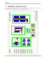
11
APPENDIX A - BOARD SCHEMATICS ...........................................................................................................79
12
APPENDIX B - REGISTERS LIST.....................................................................................................................90
13
APPENDIX C - BACKUP CD..............................................................................................................................91
14
APPENDIX D – NORSE MYTHOLOGY...........................................................................................................93
II
Per tutto ciò che è
incrocio perfetto
fra arte e scienza
varrà ancora la pena
alzarsi domani.
“Freja”, A.Borga
1
Reference: LHCb 2004-XX Control
Introduction
«What are we? Where do we come from? Where are we going? »
Those could be the usual starting questions of a scientific treatise, interrogations that mankind’s
curiosity always tried to answer, sometimes with good results but often without any sure certainties.
This introduction doesn’t aim at the explanation of those tricky queries, it focus instead on giving
an answer of a more simple question that can still turnout to be complex due to the hundreds of
“faces” that the subject of analysis can show: «What is CERN? And what do people do there? ».
An obvious answer that is related with the previous questions could be: «Well… At CERN
people try to find the answers to the above questions! ». Too vague maybe. «It is the place where the
WEB was born than! », this is true, but internet is just a small invention comparing to CERN’s final
goal.
Let’s proceed with order then, and try to reply stating facts.
CERN was founded in 1954 just after the end of the Second World War by a group of scientists
with the aim to study and reveal the building blocks of matter, the forces that bind nature and, not
least, to gather people with a common love and passion for science, innovative technologies and, of
course, particle physics.
To discover and study matter physicist use particle colliders: like children try head-on colliding
cars to see how much they can resist, scientists “play” with atomic and sub-atomic particles at high
energies to see what “comes out”.
By experimental experience it was possible to prove the existence of the quarks, much smaller
than the bricks of Bohr’s atom model which are electrons, protons or neutrons; but studies at CERN
also revealed the existence of particles which don’t exist in the actual universe… how is this
possible? There are no mysteries apparently, the physicists found a way to also “travel back in time”
using particles accelerators: even if absent in the present days’ nature and space, matter created and
studied at very high energy existed in the universe at its early stages when it was no older than a
fraction of a second.
The more energy that is put in the collisions the more far back in time physicists can look: the
LHC (Large Hadron Collider), CERN’s new particle accelerator that will start working in 2007, will
operate at an energy of 7TeV. At the energy of LHC, a small-scale reconstruction of the universe at a
time of 10-10 second after its birth will be analyzed.
Greedy machines, the four detector of the experiments (Atlas, CMS, Alice and LHCb), installed
in the 27km under ground ring will observe from different point of view what happens at the
collision points.
The Universe started out 13.7 billion years ago as an extremely hot, dense and homogenous soup
of energy and particles. The energy was continuously converted into pairs of matter and antimatter.
As the matter and antimatter collided they annihilated each other recreating energy. Hence there was
a perfect balance between matter and antimatter. After the big bang the universe started its expansion
and cooling. These phenomena provoked a series of drastic changes in its composition which led
matter to take over antimatter. Nowadays then, we live in a “matter dominated” world, but why did
this happen? The LHCb (Large Hadron Collider Beauty) experiment [3] will try to find the
explanation to this preference of nature by operating measurements on particular particles, the beauty
quarks.
Like their predecessors, LHCb and all the other experiments require ultra-modern technology to
operate in the most efficient way. The Web for example was invented in 1992 at the time of the LEP
(Large Electron Positron collider) experiment to exchange and share, in a completely new fashion,
information and data between the physicists working at CERN. As history tell us, the idea of the
project turned out to be so powerful that it was then shared and extended to the whole world.
1
“Freja”, A.Borga
Engineers and computer scientists work in close contact with physicists to help with their
knowledge the development of what can sometimes appear to be “crazy thoughts” or “science fiction
ideas” only.
Researchers are working hard trying to make dreams come true, seeking answers to millenary
questions. “Maybe there is just the hand of a god behind all that… who knows…”, though, what has
been discovered up to now need strong confirmations, no body has the arrogance to state that man is
capable to create something that never existed. Scientists are sceptic by definition and for that reason
will keep patiently looking for reasonable explanations.
And then… we will see…
2
“Freja”, A.Borga
2
Me and my work at CERN
I came to CERN in June 2003 after three years of Telecommunication engineering at the
Politecnico di Torino to start a technical studentship focused on electronics design. My high school
background in electronics allowed me to start learning with good basis while the engineering
approach, learnt at university, helped on facing problems in a more structured way… but still, more
than one year “of CERN” taught me many things about ultra-modern electronics both theoretical and
practical. Beside the pure scientific knowledge that I gathered since the day I came, CERN gave me
the opportunity to work with international people in an international environment contributing to
open my mind toward many cultures and realities completely different from mine.
When I first arrived I spent a few weeks taking over the work of Ramy Abdel-Rahman, which
drew the first sketches of the schematics of the test board. Together with my supervisor Richard
Jacobsson, lots of revisions, modifications and improvements were implemented before the layouting
process started. The board has been routed taking into consideration the base lines of 9U VME board
standard and the precious suggestions of Zbigniew Guzik who designed all the others TFC boards.
I also gave support and supervision during the whole PCB manufacturing and mounting process
to improve the board according to the indications and needs of the workshop personnel.
The development of the firmware and control software has been done in parallel with the board
debugging in a bidirectional manner: test software was developed to debug hardware and hardware
has been used to debug software. The integration of the board inside the system architecture started
from the development of self-test routines to debug the hardware and then moved step by step toward
the whole chain testing incrementing the functionalities of which the board is capable.
Once software and hardware were sufficiently developed many prototype and pre-production
tests were done in the lab giving me the possibility to spend time measuring and “hacking” on all the
TFC boards, building small devices to improve the tests and developing other tiny ideas which led to
satisfying results.
Two versions of Freja were produced: a first “final prototype” including two PCB manufactured
and one mounted, and “final version”, with two PCB both mounted, differing from the first one by
little bug fixes and small improvements. Those four boards will provide the necessary functionalities
to the TFC system for the whole experiment life.
3
“Freja”, A.Borga
4
“Freja”, A.Borga
3
TFC System Overview
3.1
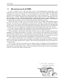
The LHCb detector
The LHCb detector will be installed about 100m underground in the cavern of LHC Pit 8, around
one of the collision points of the LHC collider.
The detector is structured as a sequence of sub-detectors organized like a lying pyramid. In total
it measures 20m in length and 10m in height. The sub-detectors are based on different technologies
and detection principles in order to reconstruct fully the particle reaction; in particular they provide
information about the structure of the collision through particle tracking, the particle energies and
momenta, and their identities. The information comes out of the detector as electronic signals which
are recorded by the data acquisition system.
Figure 1: Schematic view of the LHcb detector.
5
“Freja”, A.Borga
3.2
LHCb readout system
The figure below (Figure 2) shows a simplified picture of the entire LHCb readout system
architecture [4].
Detector
VELO
ST
OT
RIC H
ECAL
HCAL MUON
L0 FE
L0 FE
L0 FE
L0 FE
L0 FE
L0 FE
L0 FE
L1 FE
L1 FE
L1 FE
L1 FE
L1 FE
L1 FE
L1 FE
TFC
SYSTEM
SWITCH
L1 SORTER
SWITCH
L1
SWITCH
Event building
L0
LHC CLK
L1
SWITCH
READOUT NETWORK
SFC
SFC
SFC
SFC
SFC
Front-End
L0 TRIGGER
SFC
SWITCH SWITCH SWITCH SWITCH SWITCH SWITCH
C C C C C C C C
P P P P P P P P
U U UU U UUU
C C C C
P P P P
U UU U
C C C C
P P P P
U UUU
C C C C
P P P P
U UUU
CC C C
PP P P
UUUU
CPU farm
Figure 2: A simplified picture of the LHCb readout system architecture
Collisions taking place inside the detector are read out from the Front End electronics at a rate of
40 MHz. The big amount of data is too heavy to handle entirely and lots of events are not of physics
interest; for those reasons the readout system features two levels of high-rate triggers: a Level 0 (L0)
trigger that brings down the physics interaction rate of 10 MHz to an event accept rate of maximum
1.1 MHz, and a Level 1 (L1) trigger with an accept rate of maximum 40 kHz. The L0 trigger
processing is carried out in a dedicated hardware module whereas the L1 trigger processing takes
place in the CPU farm.
The architecture of the Front-End (FE) electronics reflects this two level structure in that it
consists of a L0 part and a L1 part. The L0 Front-End (L0 FE) electronics samples the signals from
the detector (at a rate of 40 MHz) and stores them during the L0 trigger processing (4 µs). The event
data are subsequently de-randomized before being handed over to the L1 FE electronics. The L1 FE
has two channels to the event building network, one of which is used to transmit event data to the L1
trigger processing and the other which is used for the complete readout after the L1 trigger decision.
Thus, upon receiving event data from the L0 FE, the L1 FE electronics sends a part of the data
over the event building network for the L1 trigger processing and buffers the complete event data
during the L1 trigger latency (58 ms). Upon receiving a positive decision the L1 FE de-randomizes
the events, zero-suppresses the data, and finally sends the complete event data to the CPU farm for
the High Level Trigger processing.
6
“Freja”, A.Borga
3.3
The TFC System architecture
The Timing and Fast Control (TFC) system is responsible for controlling the LHCb readout by
distributing timing, trigger and synchronous commands to the LHCb front-end electronics (Figure 3).
It is different from the equivalent systems of the other LHC experiments in that it has to support the
two levels of high-rate triggers. As the name itself suggests the system is responsible for:
1. Timing: the system must provide a clock, with minimum jitter, for means to archive timing
alignment of the front-end electronics.
2. Fast control: provides trigger control and distribution and data routing. The system must also
incorporate functionality to prevent buffer overflows in the entire readout chain, and provide
means of different types of auto-triggering for tests and calibration.
In order to simplify the implementation of a partitionable system, the TFC master ship of a
configurable ensemble of front-end electronics is centralized in one module: the Readout Supervisor
[5].
RS
RS
Throttle OR/Switch
VELO FE
Clock
L0 / L1
Orbit
Clock
L0 / L1
Orbit
Clock
L0 / L1
Orbit
Orbit
Clock
RS
ST FE
RS
Clock
L0 / L1
Orbit
Local trigger
(Optional)
Physics trigger
RS
TFC Switch
OT FE
RICH FE
ECAL FE
...
Event building network
Figure 3: The logical layout of the TFC architecture showing an example of partitioning.
The sub-system VELO FE is driven by the leftmost RS triggered internally.
The other sub-systems are driven by the RS in the centre connected to the LHCb trigger system.
The other RS’ are unused.
For separate local runs of sub-systems a programmable patch panel, the TFC Switch, allows
associating sub-systems to the different optional Readout Supervisors: they may thus be configured
to sustain completely different timing, triggering, and control, and can also be connected to local
trigger sources.
7
“Freja”, A.Borga
The TFC Switch distributes in parallel the information from the Readout Supervisors to the
Front-End electronics of the different sub-systems. The information transmitted by the Readout
Supervisors to the Front-End electronics via the TFC Switch and the TTC distribution network
consists specifically of:
1. The LHC reference clock at ~40 MHz as received from the LHC timing generators. This is
the master clock of all the electronics.
2. The two levels of high-rate trigger decisions (L0 and L1).
3. Commands resetting event related counters in the Front-End electronics used to identify the
accepted events and to check synchronisation.
4. Commands resetting the Front-End electronics in order to prepare it for data taking or to
recover from an error condition.
5. Calibration commands activating specific calibration systems in the Front-End electronics or
in the sub-detectors.
6. IP/Ethernet addresses assigning the CPU farm destinations to the L1 trigger data and the full
event readout.
If the physics trigger rate gets abnormally high or data congestion occurs in the event building
network, there is a potential risk of overflow in the buffers of the Front-End electronics. In order to
prevent this, the Readout Supervisor controls the trigger rates according to the status of the buffers.
Whereas the status of the fast buffers can only be known by emulating them centrally in the Readout
Supervisor, slower buffers are monitored locally. In case they are monitored locally, imminent
overflows are signalled via a dedicated throttle network. The Throttle Switch feeds back the buffer
overflow warning signals from the slower buffers in the readout to the appropriate Readout
Supervisor.
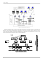
Figure 4 shows a detailed view of the TFC architecture. The Throttle ORs function as concentrators
of buffer overflow warning signals from the FE electronics and make a logical OR of the signals
within the same sub-system. The TTC modules in Figure 4 are all standard components of the CERN
TTC system (see Section 3.7).
L0
L1
Clock receiver
and fanout
LHC clock
Trigger splitter
Trigger splitter
L1
Readout
Supervisor
Readout
Supervisor
L0 Throttle switch
TTCtx
Readout
Supervisor
L1 Throttle switch
TFC switch
TTCtx
TTCoc
TTCtx
TTCoc
TTCoc
TTCoc
TTCrx
TTCrx
TTCrx
TTCrx
TTCrx
TTCrx
TTCrx
TTCrx
TTCrx
TTCrx
TTCrx
TTCrx
VELO
VELO
L1
L1FE
FE
TTCtx
TTC system
ECAL
VELO
VELO
VELO
L0
FE
L0
FE
L0
L0FE
FE
Throttle OR
VELO
VELO
VELO
VELO
L0
FE
L0
FE
L0
L0FE
FE
TTCtx
ECAL
VELO
L1
L1FE
FE
Throttle OR
L0
Local trigger
(optional)
Figure 4: Overview of the TFC architecture.
8
“Freja”, A.Borga
Summarizing, the TFC controls the readout part of the system accomplishing three main tasks
using three main boards:
1. Control, monitoring and test runs: control is done by one of the Readout Supervisors in the
pool and monitoring and test runs can be done by the others.
2. Partitioning: implemented via the TFC switch with the aim of easing the accomplishment of
different task at the same time (e.g. physics taking and detector debugging), focused monitor
testing on detector sub-parts without stopping a run.
3. Feedback: done by the Throttle Switch in order to give back-pressure to maintain the readout
speed below the throughput limit of the Data AcQuisition system (DAQ).
In the next paragraphs a more detailed description of each sub-part is given.
3.4
Readout Supervisor: “ODIN”
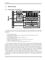
The Readout Supervisor is a complex board responsible for a multitude of functions (Figure 5).
The speed requirements and the multifunctionality of the readout supervisor necessitate optimal
technological solutions. At the same time the logic must be modifiable to support extensions or
changes in the running modes.
Throttles
ECS
L0
LHC clock L1
Trigger
generator
ECS interface
L1 broadcast
generator
Trigger
controller
Cmd broadcast
generator
Front-End
TTC Encoder
Event building
TTC
Figure 5: Simplified logical diagram of the Readout Supervisor showing the basic functions.
The TTC encoder circuit incorporated in each Readout Supervisor receives directly the LHC
clock and the LHC orbit signal via a TTC machine interface (TTCmi). The clock is distributed on the
board in a star fashion and is transmitted to all synchronous destinations via the TTC system.
The Readout Supervisor receives the L0 trigger decision from the central L0 trigger Decision
Unit (L0DU), or from an optional local trigger unit, together with the Bunch Crossing ID. In order to
adjust the global latency of the entire L0 trigger path to a total of 160 cycles (4 µs), the Readout
Supervisor has a pipeline of programmable length at the input of the L0 trigger. Provided no other
changes are made to the system, the depth of the pipeline is set once and for all during the
commissioning with the first timing alignment.
The Bunch Crossing ID received from the L0DU is compared to the expected value from an
internal counter in order to verify that the L0DU is synchronized.
9
“Freja”, A.Borga
For each L0 trigger accept, the source of the trigger (3-bit encoded) together with a 2-bit Bunch
Crossing ID, a 12-bit L0 Event ID (number of L0 triggers accepted), and a “force bit” is stored in a
FIFO. The force bit indicates that the trigger has been forced and that consequently the L1 trigger
decision should be made positive, irrespective of the L1 physics trigger. The information in the FIFO
is read out at the arrival of the corresponding L1 trigger.
The RS receives the L1 trigger decision with a 2-bit Bunch Crossing ID and a 12-bit L0 Event
ID. If the force bit is set the decision is converted to positive. The 3-bit trigger type and 2 bits of the
L0 Event ID are subsequently transmitted as a short broadcast according to the format in Table 1.
The Readout Supervisor controls the trigger rates according to the status of the buffers in the
system in order to prevent overflows. Due to the distance and the high trigger rate, the L0 FE buffer
occupancy cannot be controlled in a direct way. However, as the buffer activity is completely
deterministic, the RS has a state machine to emulate the occupancy. This is also the case for the L1
FE buffers. In case an overflow is imminent the RS throttles the trigger, which in reality is achieved
by converting trigger accepts into rejects. The slower buffers and the event-building components
feed back throttle signals via the dedicated throttle network to the RS (Figure 4). Data congestion at
the level of the High Level Trigger farm is signalled via the Experiment Control System (ECS) to the
onboard ECS interface, which can also throttle the triggers. For monitoring and debugging, the RS
has history buffers that log all changes on the throttle lines.
The RS provides several means for auto-triggering. It incorporates two independent uniform
pseudo-random generators of L0 and L1 triggers according. The RS also has a unit running several
state machines synchronized to the LHC orbit signal for periodic triggering of a single or a specified
number of consecutive bunch crossings (timing alignment), triggering at a programmable time after
sending a command to fire a calibration pulse, triggering at a given time on command via the ECS
interface etc. The source of the trigger is encoded in the 3-bit L1 trigger qualifier.
The RS has also the task of transmitting various reset commands. For this purpose it has a unit
running several state machine, also synchronized to the orbit signal, for transmitting Bunch Counter
Resets, Event Counter Resets, L0 FE electronics reset, L1 + L0 FE electronics reset, L1 Event ID
resets etc. The RS can be programmed to send the commands regularly or solely on command via the
ECS interface.
The RS transmits the IP/Ethernet destination for the L1 event data and for the complete readout as
long broadcasts.
The transmission of the various broadcasts is handled according to a priority scheme. The Bunch
Counter and the Event Counter Reset have highest priority. Any clashing broadcast is postponed
until the first broadcast is ready (L1 trigger broadcast, IP/Ethernet destination) or until the next LHC
orbit (reset, calibration pulse, and all miscellaneous commands).
The RS keeps a large set of counters that record its performance and the performance of the
experiment (dead-time etc.). In order to get a consistent picture of the status of the system, all
counters are sampled simultaneously in temporary buffers waiting to be read out via the onboard
ECS interface. The RS also incorporates a series of buffers analogous to a normal Front-End chain to
record local event information and provide the Data AcQuisition (DAQ) system with the data on an
event-by-event basis. The “RS data block” contains the “true” bunch crossing ID and the Event
Number, and is merged with the other event data fragments during the event building.
10
“Freja”, A.Borga
Pool of Readout Supervisors
ECS
MULTIPLEXERS
ECS
interface
DELAYS
V SOR
E TT I
L
C
O
H
...
as TTC encoded electrical
TFC Switch: “THOR”
TTC information
3.5
Figure 6: Diagram of the TFC switch.
As mentioned before, the TFC Switch (Figure 6) realises the partitioning of the TFC system. It is
a programmable patch panel (not a switch in the network sense) that allows distribution of the
synchronous information to the different parts of the Front-End electronics.
From the architecture of the TFC system, it follows that the Front-End electronics that is fed by
the same output of the TFC Switch is receiving the same timing, trigger and control information. The
connectivity provided by the board is not necessarily one-to-one: the TFC Switch should allow
setting up several partitions, by associating a number of partition elements (e.g. sub-detectors), to
several Readout Supervisors in order to accomplish different tasks. For example while the main RS
is controlling the detectors for data taking, the optional Readout Supervisors have the possibility of
running separately on other detector parts for test and debugging purposes.
The TFC Switch has been designed as a 16x16 switch and thus allows the LHCb detector to be
divided in 16 “atomic” sub-systems. To increase the partition granularity an option exists whereby
four TFC Switches are deployed in order to divide the LHCb detector into 32 sub-systems. The TFC
switch configuration setup is done remotely by software via the control system interface.
3.6
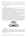
Throttle Switch and Throttle OR: “MUNIN” and “HUGIN”
Pool of Readout Supervisors
OR logic and history buffer
V S O R
E T T I
L
C
O
H
ECS
interface
Throttle signals
ECS
...
Figure 7: Diagram of the Throttle Switch.
Opposite to the data flow provided through the TFC switch, a Throttle Switch (Figure 7) has been
designed with the aim of providing backward paths of throttle signals (in case of imminent buffer
overflows) from the end buffers in the L1 front end electronics to the appropriate Readout
Supervisor. The functionality of this module is specular to the one used in the TFC switch: several
input signals are OR'ed to produce a single output signal.
11
“Freja”, A.Borga
The module has both 16 electrical and optical inputs and 16 electrical outputs. Besides providing the
ORing and the routing of the throttle signals the Throttle Switch also trace the behaviour of all input
and output signals with a good time resolution.
In addition to the Throttle Switch, a Throttle OR will be designed to group throttle lines
belonging to the same partition elements. It is identical to the Throttle Switch in all aspects except
that it ORs 20 L0 and 20 L1 throttle inputs and transmits then on a L0 and a L1 output.
Those components too are software configurable via the control system interface.
3.7
TTC Distribution System
The TFC distribution network is based on the RD12 Trigger, Timing and Control (TTC) system:
a CERN standard optical network used by all four LHC experiment [7]. The TTC system distributes
information optically on two serial channels:
•
•
Channel A: transmits the LHCb L0 trigger decisions to the Front-End electronics in the form
of an accept/reject signal at 40 MHz.
Channel B: transmits framed and formatted broadcasts, including Hamming code. Two types
of broadcasts are available: 16 bit frames which have 8 bits of user information, so called
short broadcasts (Table 1), and 42 bit frames which have 16 bits of user information (8 bit
data/8 bit address), so called long broadcasts (Table 2). It is used for several functions like:
transmission of the commands to reset the Bunch Counters (BCR) and the Event Counters
(ECR) in the Front-End electronics and the trigger systems; transmission of the L1 trigger
decision and of the Front-End control commands (e.g. calibration pulse triggering).
Table 1: Summary of the short broadcasts in LHCb.
L1 trigger
7
1
6
5
Trigger type
4
3
2
1
0
0
0
L0 FE
ECR
BCR
0
0
0
0
L0 EvID
Reset
0
1
R
L1 EvID
Calibration
0
0
0
1
Command
0
0
1
L1 FE
Pulse type
Command type
Table 2: Summary of the long broadcasts for the IP destination assignments in LHCb.
L1 IP destination
15
1
14
0
13
0
12
Flush
11
R
10
R
HLT IP destination
1
0
1
Flush
R
R
9
8
7
6
5
4
3
2
Ethernet/IP address
1
0
Ethernet/IP address
The two channels are time division multiplexed (TDM) and bi-phase mark encoded before being
converted to an optical signal. The bi-phase signal also allows transmitting the clock with low jitter.
The encoding is done in the Readout Supervisor with the TTC Readout Supervisor (TTCrs) module
and the electrical to optical conversion is done by the TTC Transmitter (TTCtx) modules, which have
14 high-power transmitters. The optical fan-out TTC Optical Couplers (TTCoc) allows distributing
the signal to 32 destinations, which means that one TTCtx can drive up to 448 destinations. The TTC
Receiver (TTCrx) ASIC reconstructs the 40 MHz clock and converts the encoded signal into the user
information. The TTCrx also provides means to adjust the timing of the TTC information in order to
time-align all Front-End boards. A version of the TTCrx, mounted on a mezzanine (TTCrm), is also
available if an easier access to the chip is needed, like for example, for debugging purposes.
Another TTC module, the TTC machine interface (TTCmi), interfaces the local experiment TTC
system with the accelerator timing system. It’s responsible of providing the LHC clock and the LHC
orbit signal.
12
“Freja”, A.Borga
4
Testing methodologies
4.1
Introduction to hardware testing
Although standard testing methodologies were initially developed for software debugging, the
definitions described below can fit perfectly hardware testing.
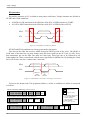
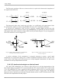
Two main categories of test setups are widely used:
1. Black box testing: functional testing.
Stimuli
T
E
S
T
B
O
A
R
D
BLACK
BOX
Black box focuses on purely functional testing. Test
routines are written knowing only the system
requirements, the inputs and the outputs (the box is
“closed”). The internal structure and implementation are
therefore ignored by the tester. To give a better hardware
view, these kinds of test are called “in the crate”.
Response
Figure 8: Black box configuration.
2. Glass (white) box testing: focused testing.
Stimuli
T
E
S
T
B
O
A
R
D
GLASS
BOX
Glass box testing applies a more direct strategy by
focusing on testing the implementation. The internal
structure and composition is accessible (the box is
“transparent”). Knowing it, the tester can try to find out
which is the best testing approach. Information about the
system can be also used to test particular features or to
obtain specific results. Again for a good hardware
analogy these tests are called “on the table”.
Response
Figure 9: Glass box configuration.
White box testing can be split in other subcategories:
a. Static: the system is not running. This is the case for onboard measurements to detect
for examples bad contacts between pins and pads, transmission lines malfunctioning,
etc.
b. Dynamic: this is “common” testing. It involves probing the system while it’s running.
Testing rarely only involves one of the methods: a complete verification is achieved only by a
good combination of both.
13
“Freja”, A.Borga
4.2
Testing theory
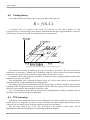
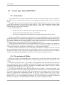
In a mathematical form testing can be expressed in the following way:
R = f (S , C )
A Response (R) of a system is the result of a function (f) fed with a Stimuli (S) and
Configurations (C) selected by the user inside a multi-dimensional space. Figure 10 shows a response
of the system in a test space with one stimulus and one configuration:
Figure 10: Three dimensional plot of the system test space.
The stimuli are selected according to the type of test that is performed. The test can either be
constructive or destructive: stimuli can be within the range of correct values to test normal running
behaviour or the system can be exposed to faulty stimuli to test error recovery.
A stimulus can be either purposive (periodic) or random to ensure coupling and decoupling of the
system from its previous stimuli.
The configuration axis is scanned in discrete steps: it is in fact often useless or not possible to
setup the board in certain combination of configurations.
According to the allowed configurations and the chosen range of stimuli, which are often selected
according to the configuration in use, it is possible to define existence regions for the testing function
which are represented by the rectangles on the above plot.
It is very important to define the test (Stimuli and Configurations) carefully to optimize the test
procedure, not to end up testing all combination.
4.3
TFC test setup
With Section 4.2 in mind the aim has been to implement a test bench which has a unit to produce
stimuli and receive responses. In order to make verification the unit emulates functionalities of the
system in test. A control system configures and sets up the test procedures.
The test unit, called Freja, of the TFC test bench is the subject of this report. All its
functionalities and a detail description are following in the next chapters.
14
“Freja”, A.Borga
Two kind of test are made for the TFC:
1. Single board test.
Since the Readout Supervisor is the most complex
board of the TFC system it requires focused tests.
Referring to the device description made in
Section 3.4 the test will concentrate on debugging
the following features:
• L0 trigger path
• L1 trigger path
• Buffer level control
• IP destination broadcasting
Figure 11: Single board test configuration.
2. Full TFC system testing.
electrical
optical
L1 path (LVDS)
L0 path (LVDS)
Throttle path (LVDS)
Figure 12: Full TFC system test configuration.
The test board emulates both the L0 and L1
decision units (L0 trigger and L1 trigger in
Figure 2) sending decisions to the Readout
Supervisor; the decisions are then transmitted to
the Front-end electronics (L0 and L1 FE
emulated by the test board) via the whole TFC
chain: TFC switch and TTC distribution
network. The test board can speed up the
decision sending in order to overflow the
buffers in the Readout Supervisor or in the
Front End: this technique is used to check the
throttle backward path and the buffer emulation
(via the throttle switch).
The aim of Freja is to perform black box testing of all the functionality of the boards in the setups
listed above. As mentioned before black box testing and glass box testing are complementary and
black box testing will help the testers to discover bugs which will be subsequently debugged using
glass box testing.
For example: a test aim is to check if a data bus is clean, complete (no bits missing), well driven
and arbitrated and pass all the way trough its designed path. A black box test done with the test board
will consist in feeding data pattern and driving the control bus lines of the target board via a known
bus input and receive them back from a known bus output. Afterwards the board will compute the
received signal (checks the data integrity, delays, etc) and decide if it’s correct or not. If the result is
correct the test is over and successful. If not one must switch to glass box tests: measurements can
start from the path check to make sure that signals are propagated properly all the way down, if the
path is interrupted somewhere the test focus then on the chip or line that causes interruptions, if the
signals shapes are ruined but none on the chip driving has an odd behaviour, the test can move to
neighbouring parts of the board. A careful combination between the two tests and a bit of method
and intuition will always drive a tester to a solution.
15
“Freja”, A.Borga
4.4
Application of Freja
Freja is a general purpose board which allows it to be used in the TFC system in several
applications for a very long time. Many different purposes were conceived and studied already in the
early stages of the conception. Here after they are discuss in more details.
4.4.1 Prototype testing
Prototyping phase is the most critical part of all. The complete set of features of the TFC has to
be tested extremely carefully in order to lunch the production of a 100% working product. Prototype
testing involves tests on parts that will not be changed (except in case of future development and
improvements), like the hardware. Another point to concentrate on during prototype testing is to find
a good set of “well known” problems that will ease life on production testing: for example if a
particular component follows a difficult mounting technique (like dense, impedance matched
connectors, fine pitch ICs, etc) and problems are discovered during prototype testing, it will be
important to check carefully it on all the produced boards. Error recovery testing is fundamental as
well in this phase: it’s important to know how the system reacts and recover from certain error
conditions, how long it takes and if afterwards it can be considered stable again.
4.4.2 Pre-production and production testing
This phase makes use of all the experience gathered during prototype testing. Test bed contains a
full set of testing and debugging tools (see following chapters) in order to speed the procedures.
4.4.3 Commissioning
“You have a board perfectly working on your lab table… you bring it down to the pit, plug it into
the crate… and suddenly everything goes wrong!” this is a nightmare that very often scares
technicians, engineers and physicists and the reason why a test board can be very useful to test
board-to-board functioning and compatibility during commissioning. In situ architecture and
installation tests aim at solving these kinds of problems: Freja will perform the standard test routines,
developed in the lab environment, on the TFC boards in the barracks of Pit 8 (LHCb installation
site). Since the TFC installation will take place long before the installation of the detectors with their
electronics, Freja will allow the TFC system to be tested without the final front-ends.
4.4.4 Experiment monitoring
Freja will be an independent implementation of a Front End electronics to perform system tests
together with idle Readout Supervisors. The test board will also perform simple TTC system
monitoring, tuning alignment between detectors and cross checking of the connectivity of the entire
TFC system.
16
“Freja”, A.Borga
5
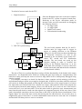
TFC test board: “FREJA”
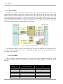
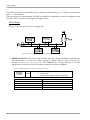
5.1
Overview of the board
Figure 13: A block diagram of the TFC test board.
The board consists of seven main blocks with different functions and using different electronics:
1. Control interface [Section 5.2 and Section 5.3]: a Credit Card PC is accessible via remote
connection in an Ethernet network. From the CCPC the hardware is accessible via a
33MHz PCI bus. An interface card (Glue card) translates the PCI bus to the proper bus
formats to reach specific devices on board (such as FPGAs, memories, etc). Four types of
conversions are made by the Glue card:
a. JTAG: dedicated lines for the FPGA programming and boundary scan of devices.
b. I2C: standardized serial bus used to configure small devices (e.g.: serial ID
E2PROM, I2C port, TTCrx).
c. LBUS: the PLX Local Bus is a 32-bit bus used to configure, control and monitor the
functions implemented in the FPGA.
d. GPIO: general purpose input/output lines. Used in Freja to drive JTAG lines to
program the Altera configuration device (EEPROM) for the FPGA.
2. External general purpose electric I/O [Section 5.4]: to interface the test board with the
rest of the system in order to make tests, it’s important to have as many input/output
ports as possible. Two different electrical transmission techniques are used to transmit
data over the system: single ended ECL (Emitter Coupled Logic) and differential LVDS
(Low Voltage Differential Signalling).
3. Optical transmitter and receiver: the optical I/O interface of Freja is used in a
standalone mode to test the optical path of the throttle network (Munin) and to transmit
throttle signals when Freja acts like a front end board.
4. FPGA [Section 5.5]: together with an external FIFO buffer this is the core part of the
board. A programmable logic device with 168 IO ports is used to perform all functions
of Freja, drive and receive test signals, perform calculation and checks on them and
make results available to the user interface. A device configuration EEPROM is
implemented to speed up the programming process of the device at start-up.
17
“Freja”, A.Borga
Clock sources: in order to run the board in different modes a clock selection
multiplexer, accessible via I2C, has been implemented giving the possibility to select
between:
a. Internal clock: 40MHz quartz generated clock.
b. TTCrm clock: clock generated by the TTC system (experiment official clock).
c. TTCrs clock: internal or external clock coming from the TTCrs mezzanine.
d. External clock: allows the board to run with an external clock source.
6. TTCrs: TTC encoder and transmitter.
7. TTCrm: optical TTC system receiver.
5.
5.2
Credit Card PC
5.2.1 The ECS interface and the CCPC
The electronics boards in LHCb will all be controlled from the LHCb Experiment Control System
(ECS). In order to access the actual board resources, an ECS interface will be located on each board.
The ECS interface is connected to the control network and performs directly all programming,
configuration, control and monitoring of each electronics board.
Three ECS interfaces have been proposed for different applications: the SPECS (Serial Protocol
for the Experiment Control System) and the ELMB (Embedded Local Monitor Board) will be used
for electronics boards situated in the radiation area close to the experiment; for the electronics
situated in the counting rooms behind the shielding wall, the ECS interface is based on a commercial
small (credit-card size) embedded PCs used to provide the necessary local intelligence on electronic
boards [12]. They are connected to the central ECS via a conventional Ethernet.
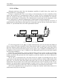
The core of the Credit-Card PC (CCPC) is a SM520PC Smart Module produced by DigitalLogic, Inc [13]. This module comprises a PC-on-a-chip also known as micro-controller, the Elan520
from AMD, an Ethernet interface and a Flash RAM. It can run any standard PC operating system and
runs Linux in LHCb. The CCPC is equipped with a 33 MHz PCI bus which is used for all access to
the board logic.
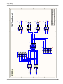
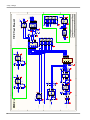
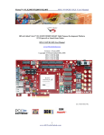
Figure 14: Picture of the "Glue light" board (right) together with the Credit Card PC (left).
18
“Freja”, A.Borga
5.2.2 PCI Interface
Currently by far the most popular local I/O bus, the Peripheral Component Interconnect (PCI)
bus, was developed by Intel and introduced with the version 1.0 in 1992. Since then several updates
(revision 2.0, revision 2.1, version 2.2 [17] and PCI-X [18]) have been made to improve not only the
bus speed but also the overall performance (bus arbitration, transmission, etc). It was geared
specifically to fifth- and sixth-generation systems (e.g. Intel Pentium and Pentium II), although the
latest generation 486 motherboards were already using it as well. Like its predecessor, the VESA
(Video Electronics Standards Association) Local Bus, PCI 1.0 was a 32-bit bus running at a
maximum frequency of 33 MHz. Since then its wide usage in electronic devices led this technology
to nowadays’ extreme edges.
The PCI bus is used to interface devices requiring fast access to each other and/or system
memory and that can be accessed by the processor at a speed close to its internal bus. A key feature
of PCI is the capability to transmit data in bursts (a single address phase is followed by two or more
data phases) whose length is set by the master. The target device receives information about the
transaction type and the start signal, but not the transfer length: while the master makes a burst of
data transactions, it signals the target device when the last word transfer occurs.
The typical PCI device includes a complete peripheral adapter encapsulated within an IC package
or implemented on an expansion card: the most famous interface device is the PLX 9030 whose
functions have inspired the development of the firmware for the Glue card (see Section 5.3).
Reflected-wave switching
At the time when bus speeds were low (below 1 MHz) the characteristics of transmission lines
were neglected by designers and the choice of the power of the driving device was selected
according to the electric characteristics (in particular the input capacitance) of the devices connected
to the lines. Using buses with clock frequencies higher than 25 MHz, traces acts as transmission lines
and the electrical characteristics of the trace must also be taken into account solving the equation that
defines the characteristics of the output driver: an impedance, varying between 50 and 110 Ohm, is
presented to the driver trying to drive a voltage change onto the line and also imposes a time delay in
the transmission of the voltage change along the trace.
An old method used to eliminate the annoying effect of the line impedance is called IncidentWave Switching. It involves the use of strong output drivers with the capability of switching close to
the driving point of the device (point of incidence). The main disadvantage of this method is that
connecting several devices on one trace increase immediately the driving current required. This
limits the packing of drivers in chips and increases the heat on board. Incident-wave switching also
requires termination on the lines.
Since this technique turned out to be inefficient, another was introduced for PCI called
Reflected-Wave Switching: no termination is required and the reflected wave is used as an advantage.
A carefully selected, relatively weak output driver is used to drive the signal line partially towards
the desired logic state. The driver only has to drive the signal line partially towards its final state,
rather than completely (as a strong incident-wave would). No inputs along the trace will sample the
signal until the next rising-edge of the clock.
When the wavefront arrives at the unterminated end of the bus, it is reflected back and doubled.
Upon passing each device input again during the wavefront’s return trip down the trace, a valid logic
level registers at the input on each device. The signal is not sampled, however, until the next risingedge of the PCI clock. Finally the wave front is absorbed by the low-impedance within the driver.
This method cuts driver size and lower by half the current needed using incident-wave witching
technique.
Diode terminations are integrated inside devices to limit reflections and correct the propagation
19
“Freja”, A.Borga
delay. Even though Reflected-wave switching has improved a lot the signal characteristic in PCI, it is
always better to swap to more versatile bus techniques as soon as possible. With the last statement in
mind the Glue card has been developed.
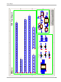
Bus signals
The PCI interface requires a minimum of 47 pins for a one-target device to handle data,
addressing, interface control, and system functions. Two additional pins, routed directly to a bus
arbiter, are required in the case of multi-master configuration for each device that intends to act as a
master on the bus.
Required pins
Address
& Data
Optional pins
AD [31...0]
AD [64...32]
nC/BE[3..0]
nC/BE[7..4]
PAR
PAR64
nREQ64
nACK64
nFRAME
nTRDY
nIRDY
nSTOP
nDEVSEL
IDSEL
Interface
Control
Error
Reporting
nPERR
nSERR
Arbitration
(master only)
nREQ
nGNT
System
CLK
nRST
PCI
COMPLIANT
DEVICE
64-Bit
Extension
nLOCK
nINTA
nINTB
nINTC
nINTD
Interface
Control
Interrupts
TDI
TDO
TCK
TMS
nTRST
JTAG
(IEEE 1149.1)
Figure 15: PCI bus signal organization.
As shown in the figure above PCI pins are organized in different groups. Below a more detailed
description of the most important pin’s function:
1. System pins:
a) CLK: provides timing for all transaction on PCI and is an input of every PCI device.
The CCPC can operate up to 33 MHz or 66 MHz (according the specification of rev
2.2); though it must be kept in mind that newer specification, like PCI-X foresee
operations of devices at a frequency up to 133 MHz.
b) nRST: PCI’s reset line.
2. Address and Data pins:
a) AD [31...0]: Address and Data are multiplexed on the same PCI pins. A bus
transaction consists of an address phase followed by one or more data phases. As
mentioned before PCI supports both read and write bursts.
b) nC/BE [3...0]: Bus Command and Byte Enables are multiplexed on the same PCI
20
“Freja”, A.Borga
3.
4.
5.
6.
pins. During the address phase the pins are used to define Bus Commands (the type of
transaction the bus is requesting). In the data phase they are used as Byte Enables
(determine which bytes are valid in the bit stream on the bus).
c) PAR: Parity is even parity across AD [31...0] and C/BE [3...0]. Parity generation is
required by all PCI devices.
Interface Control pins:
a) nFRAME: Cycle Frame is driven by the current master to indicate the beginning and
duration of an access.
b) nIRDY: Initiator Ready indicates the initiating devices’ ability to complete the current
data phase of the transaction. During write mode it indicates that valid data is present
on the address bus. During read mode it indicates that the master is prepared to accept
data.
c) nTRDY: Target Ready indicates the target devices’ ability to complete the current data
phase of the transaction. During a write operation it indicates that the target is
prepared to accept data. During a read operation it indicates that valid data is present
on the bus.
d) nSTOP: Stop indicates that the current target is requesting the master to stop the
current transaction.
e) nLOCK: Lock indicates an atomic operation to a bridge that may require multiple
transactions to complete.
f) IDSEL: Initialization Device Select is used as a chip select during configuration read
and write transaction.
g) nDEVSEL: Device Select, when actively driven, indicates that the driving device has
decoded its address as the target of the current access. As an input it indicates whether
any device on the bus has been selected.
Arbitration pins:
a) nREQ: Request indicates to the arbiter that this device desires use of the bus. This is a
point-to-point signal.
b) nGNT: Grant indicates to the device that access to the bus has been granted. This is a
point-to-point signal too.
Error Reporting pins:
a) nPERR: Parity Error is only for the reporting of data parity errors during all PCI
transaction. It is mandatory to use this control signal because the devices driving the
bus must assume that the receiver will check the correctness of the information and
flags back in case of errors. It can be neglected in case of Special Cycles (a broadcast
message to one ore more PCI devices).
b) nSERR: System Error is for reporting address parity errors, data parity errors during a
Special Cycle and critical errors (usually even catastrophic) other than parity.
Optional pins:
a) 64-Bit Extension: PCI bus can be extended up to 64-bits. This requires more control
logic of course. The PCI extension is not analyzed in detail because for TFC purposes
the 32-bit wide bus is sufficient.
b) Interrupt pins: 4 interrupt lines are reserved on the PCI bus to allow devices to
request attention from its device driver.
21
“Freja”, A.Borga
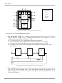
5.3
Glue Card
Since PCI is a complex and difficult bus to handle (require special attention when routing due to
tight timings and many control line) a small device is used to convert the PCI bus after a short
distance on board to more simple ones; the conversion unit is the Glue Card (the name comes from
the fact that glue logic consists of a simple circuit used to interface different devices, like the CCPC
to the board logic) implemented in a “light” version by TFC system [19]. The mezzanine is entirely
based on a single FPGA which is interfaced with the PCI bus of the CCPC and emulates a PLX 9030
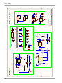
(an ASIC chip that produces a simple PLX local bus) [14].
Figure 16: Block diagram of the Glue card.
As mentioned before the Glue Card translates the PCI bus into different bus protocols (JTAG,
I2C and Local Bus) allowing access to many different types of devices. Next each bus type is
described in more details.
5.3.1 PCI slave
The PCI interface implemented in the FPGA of the Glue Card is compliant with the PCI Local
Bus Specification Revision 2.2 and emulates a PLX 9030. The target supports a 33 MHz and 32-bit
PCI bus.
Table 3: Implemented PCI bus commands.
22
CBEN [3 ... 0]
Bus Command Cycle
Note
0110
0111
1010
1011
1100
1110
1111
Memory Read
Memory Write
Configuration Read
Configuration Write
Memory Read Multiple
Memory Read Line
Memory Write and Invalidate
fully implemented
fully implemented
fully implemented
fully implemented
substituted by Memory Read
substituted by Memory Read
substituted by Memory Write
“Freja”, A.Borga
Table 3 summarizes the PCI bus commands that are supported by the Glue Card. Table 4 presents
the PCI Configuration Registers. These registers are accessed by the commands “Configuration
Read” and “Configuration Write”. Only the shaded fields are implemented. Read accesses to the
other fields always return zero. The Configuration Registers can be accessed either in byte, word or
double word transfers. The first two Base Address Registers (BAR0 and BAR1) are reserved for
system use. BAR2 holds the base address of the local resources described below. Table 5 shows the
values assigned by default to the Configuration Registers.
Table 4: PCI Configuration Registers. Shaded registers have been implemented.
Address
31 ... 24
23 ... 16
15 ... 8
7 ... 0
00h
04h
08h
0Ch
10h
14h
18h
1Ch
20h
24h
28h
2Ch
30h
34h
38h
3Ch
40h - FCh
Device ID
Vendor ID
Status Register
Command Register
Class Code
Revision ID
BIST
Header Type
Latency Timer
Cache Line Size
Base Address 0 (BAR0)
Base Address 1 (BAR1)
Base Address 2 (BAR2)
Base Address 3 (BAR3)
Base Address 4 (BAR4)
Base Address 5 (BAR5)
Cardbus CIS Pointer
Subsystem ID
Subsystem Vendor ID
Expansion ROM Base Address
Reserved
Reserved
Max_Lat
Min_Gnt
Interrupt Pin
Interrupt Line
Reserved
Table 5: Default settings of the PCI Configuration Registers.
Name
Offset
Vendor ID
Device ID
00h
02h
Command Register
04h
Status Register
06h
Revision ID
Class Code
08h
09h
BAR0 – BAR2
10h
Subsystem Vendor ID
Subsystem ID
2Ch
2Dh
Value
1172h (Altera ID)
0001h
Read/Write bits:
Bit 1 – MEM_ENA
Bit 6 – PERR_ENA
Preset bits:
Bit 7 – STEP_IMPL (forced to HIGH)
Other bits hardwired to LOW
Updated Read/Write bits:
Bit 27 – TAR_ABORT (Set when no slave response)
Bit 31 – DET_PAR_ERR (Detected parity error)
Preset bits:
Bits 26..25 – DEVSEL_TIM (Set to 10)
Other bits return LOW
01h
118000h (Data acquisition + Other + None)
Bit 0
- MEM_IND (hardwired to LOW)
Bit 2..1
- MEM_TYPE (hardwired to LOW)
Bit 3
- PRE_FETCH (hardwired to LOW)
Bits 15..4 - hardwired to LOW
Bits 31..16 - r/w accessible
201Ch
0000h
23
“Freja”, A.Borga
Seen from the PCI bus, the entire user memory occupies an address range of 64 KB (16 address
lines). As shown in Table 6, the block is divided into two regions: the first 64 bytes (16 double
words) hold the Internal Registers and the rest of the space is used for the local bus accesses to the
registers on the motherboard. Accesses to the Internal Registers and the local bus transfers may only
be done as 32-bit double words via the Base Address Register 2 (BAR2) in the PCI Configuration
Register.
Table 6: Assignment in the local memory of the device.
Offset
31 .. 24
23 .. 16
00h
...
03Fh
040
...
FFFFh
15 .. 8
7 .. 0
Internal Registers (r/w) (Table 5)
Local Bus (r/w)
The Internal Registers of the Glue Card controls three areas of activity: the JTAG and the I2C
busses and the General Purpose I/O lines. In addition the Internal Registers contains a Control and
Status Register (CSR) which allows configuring several functions of the Glue card. A summary of all
the Internal Registers is given in Table 7. All unused (not shadowed) registers return zero during read
access.
In the current version of the Glue Card, the CSR (Table 8) allows enabling and disabling the
JTAG and the I2C bus and the General Purpose I/O lines. Disabling a bus puts the output pins in the
high-impedance state. The CSR also allows selecting the width of the local bus and configuring the
abort method when a time out occurs on the local bus. When a smaller local bus than 32 bits is used,
it always starts from the least significant bit.
Table 7: Assignment of the Internal Registers.
Offset
31 .. 24
00h
04h
08h
0Ch
10h
14h
18h
1Ch
20h – 3Fh
23 .. 16
15 .. 8
7 .. 0
CSR (Table 6)
JTAG_CON (Table 8)
I2C_CON (Table 9)
I2C_DAT
PIO_PORT (Table 10)
PIO_OE (Table 10)
PIO_SSET (Table 10)
PIO_SCLR (Table 10)
Reserved
Table 8: Bit assignment in the Control and Status Register (CSR). (Offset 00h in the Internal Registers).
Bits
Mnemonics
Description
24
1...0
BSIZE [1..0]
2
TMO_ABORT
3
BRST_ENA
4
5
6
7
JTAG_ENA
PIO_ENA
I2C_ENA
JTAG_TRST
00 – 8 bits bus
01 – 16 bits bus
10 -- 24 bits bus
11 – 32 bits bus
When set Target Abort is generated on a time out, this is missing slave
response. When zero a dummy cycle is generated
When set enables burst operation on the local bus, otherwise only single
data cycles are performed
Enables/disables the JTAG bus
Enables/disables the General Purpose I/O port
Enables/disables the I2C bus
JTAG reset line (active in low)
Access
Selecting the size of the local bus:
r/w
r/w
r/w
r/w
r/w
r/w
r/w
“Freja”, A.Borga
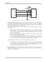
5.3.2 I2C Bus
Although serial buses don’t have the throughput capability of parallel buses, they require less
wiring and fewer IC connecting pins.
It must be remarked that a bus is not merely an interconnecting wire but it embodies all the
format and procedures for communication within the system. Devices communicating with each
other on a serial bus must have some form of protocol which avoids all possibilities of confusion,
data loss and blockage of information. The communication system must not be dependent on the
devices connected to it, otherwise modifications or improvements would be impossible.
A procedure has also to be devised which device will be in control of the bus and when. If
different devices with different clock speeds are connected to the bus, the bus clock source must be
defined. I2C specifications take care of all requirements in detail.
Figure 17: Generic I2C bus configuration.
I2C (Inter-Integrated Circuit) [20] is a simple bi-directional 2-wire bus developed by Philips in
order to control efficiently integrated circuits interconnected with few signals on electronics boards.
One line feeds the clock to the devices (Serial Clock Line, SCL) and the other carries data (Serial
Data Line, SDA). Bi-directional data transfers can be made at up to 100kbit/s in Standard-mode, up
to 400kbit/s in Fats-mode or up to 3.4Mbit/s in the High-speed mode but the last mode requires
special routing techniques.
Each device is recognized by a unique peripheral address and can operate as either a transmitter
or receiver, depending on the function of the device. A master is the device which initiates a data
transfer on the bus and generates the clock signals to permit the transfer; any device addressed is
considered a slave.
The I2C bus is a multi-master bus: more than one device capable of controlling the bus can be
connected to it; that means that more than one device master could try to initiate a data transfer at the
same time. To avoid the chaos that might ensue from such an event, an arbitration procedure is
implemented. This procedure relies on the wired-AND connection of all I2C interfaces to the I2C bus.
A master can operate both as master-transmitter or master-receiver. Since on Freja the master of the
I2C bus is always the FPGA on the Glue Card, bus arbitration is not discussed in more detail.
All I2C bus compatible devices incorporate an on-chip slow interface which allows them to be
addressed directly between each other.
25
“Freja”, A.Borga
Bit structure
Bit transfer structure on I2C is similar to many other serial buses. Unique situations are defined as
START and STOP conditions:
•
•
A HIGH to LOW transition on the SDA line while SCL is HIGH indicates a START.
A LOW to HIGH transition on the SDA line while SCL is HIGH defines a STOP.
SDA
SCL
START condition
STOP condition
Figure 18: I2C START and STOP conditions.
START and STOP conditions are always generated by the master.
The data on the SDA line must be stable during the HIGH period of the clock. The HIGH or
LOW state of the data line can only change when the clock signal on the SCL line is LOW. Every
data transaction put on the SDA line must be 8-bits long. Each byte has to be followed by an
acknowledge bit. Data is transferred with the most significant bit (MSB) first. By holding the clock
line LOW a slave can force a master into a wait state.
SDA
SCL
Data line
stable
data valid
Change of
data
allowed
Figure 19: Valid Data line transaction according to Clock status.
Freja uses the format with 7-bit peripheral address (a 10-bit is available too) which is structured
as follows:
Master-transmitter addressing a slave receiver
Master to slave
S SLAVE ADDRESS R/W A DATA A DATA A/A P
Slave to master
Master reads a slave immediately after first byte
S SLAVE ADDRESS R/W A DATA A DATA A P
A = Acknowledge (SDA LOW)
/A = not Ack (SDA HIGH)
S = START condition
Sr = repeated START condition
P = STOP condition
R/W = ‘1’ read , ‘0’ write
Combined format
S SLAVE ADDRESS R/W A DATA A/A Sr SLAVE ADDRESS R/W A DATA A/A P
Figure 20: I2C data information structure for sequential memory access.
26
“Freja”, A.Borga
Many I2C devices allow to access more than one I2C register in a non sequential mode, in this
case the structure is:
Master to slave
Slave to master
Byte write to target register in a device
S SLAVE ADDRESS 0 A WORD ADDRESS A DATA A P
A = Acknowledge (SDA LOW)
/A = not Ack (SDA HIGH)
S = START condition
Sr = repeated START condition
P = STOP condition
R/W = ‘1’ read , ‘0’ write
Random read to target register in a device
S SLAVE ADDRESS 0 A WORD ADDRESS A S SLAVE ADDRESS 1 A DATA A/A P
Figure 21: I2C data information structure for random memory access.
I2C on the glue card
The operation of the I2C bus on Freja is controlled via the PCI bus by accessing two 8-bit wide
registers in the Internal Registers: I2C_CON and I2C_DAT. The I2C_CON register provides an
interface to the I2C state machine implemented in the Glue Card FPGA. The procedure to operate the
bus follows the standard specification described before and the bit assignment in the I2C_CON
register is shown in Table 9.
Table 9: Bit assignment in the I2C control register I2C_CON (Offset 08h in the Internal Registers).
Bits
0
1
2
3
4
5
6
7
Notes:
Mnemonic
Description
Access
Error bit. Set after a bus request access failed (unsuccessfully writing
START, STOP or data or reading data). Cleared after the first valid transfer.
NOACC
Note: Writing or reading the data register I2C_DAT when DONE is low will
ro
cause this error. Also reading data while in “sending” mode or writing data
while in “receiving” mode will generate this error.
The bit indicates that the slave acknowledged the address phase (for read or
ACK
ro
write). For write transfers ACK = ‘1’ when byte is accepted.
Set after completion of the start, the data or the stop phase . Cleared after
DONE
ro
setting the START or the STOP and reading or writing the register I2C_DAT.
The bit indicates that the I2C bus is being used. It is set after setting the
BUSY
ro
START bit and it is cleared when the stop condition occurs.
When I2C_RESET is set, a reset of the entire I2C controller is performed.
I2C_RESET The reset is a momentary action and extends only over two system clock
mom
cycles.
Can be set only if DONE has been asserted. Forces no read acknowledge
LAST
r/ws
while sending data. Cleared after the stop condition occurs.
Can only be set if DONE has been asserted. It generates a stop condition. It
STOP
r/ws
is cleared when the access has been completed.
Can be set if either BUSY is LOW or DONE is HIGH. It generates the start
START
r/ws
condition. When BUSY is asserted, repeated start conditions may be
generated. Cleared after the acknowledgment in the address phase
Bits 3 ... 0 are read only
Bit 4 is a momentary write-only action bit and it doesn’t retain its value.
Bits 7... 5 are special action read/write bits. Writing a logic one to the bit sets the appropriate bit in
the register. Writing a logic zero has no effect.
Data are transferred to and from the I2C bus by writing and reading the I2C_DAT register (Table
7). The register holds the address byte during the address phase, and a byte of data to be transferred
in write mode or a received data byte in read mode.
27
“Freja”, A.Borga
The least significant bit of the address byte contains the direction flag. A “0” means a write transfer
and a ‘1’ a read transfer.
The bus frequency is approximately 100 kHz by default for compatibility. It can be configured to run
four times faster for devices that support the higher speed.
I2C on Freja
Three I2C devices are used on Freja (Figure 22):
Figure 22: Block diagram of the devices connected to I2C bus on Freja.
a) EEPROM 24LC00: small non volatile memory that stores board identification information.
This information is used by the control system to identify different types of boards (see
Section Error! Reference source not found.). The EEPROM ha a storage capacity of 128 bits
organized as 16 words of 8 bits. The memory structure is shown in Table 10.
Table 10: EEPROM physical address and internal structure.
Physical or
peripheral
address
If X bit is:
0xAX
0.
Write memory
1.
Read memory: whether random or sequential
Command byte
0x00
28
Description
System ID
[TFC]
0x01
Board Type
0x02
Board Revision
[Ver 1, Ver 2]
[Freja, Odin, etc.]
0x03
Board Number
[0, 1, 2, 3, etc.]
“Freja”, A.Borga
b) I2C REGISTER PCA9554: device used to drive the control lines of simple components on
the board. Each output line is associated and driven by an internal register (Table 11).
Table 11: I2C register physical address and control lines structure.
Physical or
peripheral
address
If X bit is:
0x4X
0.
Write memory
1.
Read memory: whether random or sequential
Command
Description
byte
Value
Comments
I/O
configuration
register
0x00
All I/O lines set to output
0x03
X
{
X
{
X
{
X
{
X
{
FPGAreset not used TTCrs reset H _ EXT * TTCrx reset
[ SRESn1]
[ SRESn 2]
X {
X
{
123
X
{
SEL 2 SEL1 not used
Clock selection
* clock source on TTCrs
0x01
Output port
register
0x14 [10100]
Internal clock
0x12 [10010]
External clock
0x10 [10000]
TTCrm clock
0x16 [10110]
TTCrs external clock
0x06 [00110]
TTCrs internal clock
c) TTCrx: the configuration of the TTC receiver chip is done via I2C. The I2C bus of this device
is based on a double register configuration: an address is written to an address register in
order to target a memory location, while data are transferred through a data register. This
access mode is thus slightly different from the one implemented with the other devices used
on the TFC boards. More details can be found in [8].
5.3.3 JTAG Bus
Boundary-Scan Testing (industry standard IEEE 1149.1 [22]) was developed in the mid-1980s by
the Joint Test Action Group (JTAG) to detect physical faults on PCBs caused by increasingly
crowded assemblies due to novel packaging technologies, such as today’s BGA packages.
In space-constrained environments, or high-speed designs, it’s not always possible to incorporate
test pads that link the PCB to an ATE (Automatic Test Equipment) bed-of-nails interface. Boundaryscan embeds test circuitry at chip level to form a complete board-level test protocol. With boundaryscan is it possible to access even the most complex assemblies for finding and diagnosing hardware
problems but also perform In System device Programming (ISP).
Figure 23 shows a block diagram of the JTAG components integrated inside boundary-scanable
devices. The test logic consists of an instruction register and a controller and is accessed through a
Test Access Port (TAP). The boundary scan technique involves the inclusion of a shift-register stage
(contained in a boundary-scan register cell) connected to each component pin so that signals at
component boundaries can be driven and read using scan testing principles.
29
“Freja”, A.Borga
JTAG Instructions:
BSR
Core
logic
TDI
1.
Extest
2.
Bypass
3.
Read-ID
4.
Private
TDO
Instruction
register
TMS
TAP
controller
TCK
Figure 23: Internal structure of JTAG boundary-scanable IC.
An overview of JTAG building blocks follows:
1. Test Access Port (TAP): it is a general purpose port that provides access to all the test
support functions integrated in a boundary-scanable device. Four signals are used to
configure and communicate to and from a TAP:
a) Test Clock Input (TCK): a clock separate from the system clock.
b) Test Data In (TDI): data is shifted into the JTAG-compliant device via TDI.
c) Test Data Out (TDO): data shifted out the JTAG-compliant device via TDO.
d) Test Mode Select (TMS): TMS commands select test modes as defined in the JTAG
specification.
IC1
TDI
IC2
TDO
TDI
ICn
TDO
TDI
TDO
TMS
TCK
TDO
Figure 24: Configuration of JTAG devices with a serial connection.
2. TAP controller: the TAP controller is a state machine that provides access to the functions
built into the JTAG-compliant device. The state machine controls all operations for the
JTAG-compliant device. A user can sequence through the state machine functions via the
TCK and TMS inputs.
30
“Freja”, A.Borga
Figure 25: Configuration of the termination resistors of the JTAG line.
3. Instruction register: instructions used to select the test to be performed or the data register
to be accessed are shifted into the design by the instruction register. A number of mandatory
operations are defined by JTAG specification but design-specific instruction can be added as
well to extend the functionalities of the test logic.
The instruction register allows selection of the following compulsory registers and their
relative functions:
a. Bypass: reduces the BSC shift path through the device to a single bit register.
This instruction is used when a direct operation into only some devices of the chain
has to be done: bypass allows the user to bypass BSCs inside an IC to pass data
directly into another chip.
b. Sample/preload: instruction used either to sample the data currently contained in the
BSCs, or to preload data into the BSCs.
c. Extest: when extest is performed the BSCs attached to the JTAG device input pins act
as sensors while the BSCs attached to output pins propagates data to interconnecting
devices. The interconnecting devices may or may not be JTAG-compliant.
Optional instructions which are very often implemented by chip designers are:
d. Usercode/Idcode: instructions used to serially read a code from a target component.
Use of the Idcode will provide information on the base component, while use of the
Userdcode will provide information on the particular programming of an on-board
component (e.g. used to program TFC FPGAs).
4. Test data registers: the test logic architecture contains a minimum of two test data registers.
Selection of the register that forms the serial path at a given time is controlled from the
instruction register (Figure 26).
31
“Freja”, A.Borga
Figure 26: Test data registers.
a. The bypass register: provides a single-bit connection through the circuit when none of
the other test data register is selected. This register can, for example, be used to allow
test data flow through a device without affecting his BSCs.
b. The boundary-scan register: this allows testing of board interconnections, detecting
typical production defect such as opens, shorts, etc. It also allows access to the inputs
and outputs of components when testing their system logic or sampling of signals
flowing through the system input and outputs.
c. The device identification register: optional test data register used determine for
example device’s manufacturer, part number, etc.
d. The design-specific test data register: optional registers may be provided to allow
access to design-specific test support features. The manufactures of programmable
devices use this register to implement the programming interface. This will be
discussed in more details in Section 5.5.5 and 5.5.6.
5. Boundary-Scan Register (BSR): each IO pin of an Integrated Circuit (IC) is connected to
three cells, each known as Boundary-Scan Cell (BSC), of a shift-register (
6. Figure 27). The cells link the JTAG circuitry to the IC’s I/O logic. All BSCs of a particular
device constitute a Boundary-Scan Register (BSR). BSR logic becomes active when
performing JTAG testing, otherwise under normal IC operation it remains passive.
si
Input Cell
Control
Cell
I/O
Output
Cell
so
Figure 27: Structure of a Boundary-Scan Register.
32
“Freja”, A.Borga
JTAG on the glue card
The JTAG bus of the Glue Card is driven directly via the PCI bus by accessing the JTAG_CON
register (Table 12) in the Internal Registers (Table 7).
In a read access the first four bits reflects the state of the JTAG bus lines. Transactions on the
JTAG bus are performed by writing to the register.
The states of the TCK, the TDI and the TMS output lines are set by writing commands to the
three two-bit registers that in a write access are associated with the three lines.
The set/clear operations are defined in Table 12. JTAG transactions are thus made by putting data
on the TMS and the TDI lines and toggle the clock line TCK, and by reading the TDO line.
Table 12: Bit assignment in the JTAG control register JTAG_CON (Offset 04h in the Internal Registers).
Bits
Read Access
0
Read state of TCK line
1
Read state of TMS line
2
Read state of TDI line
3
Read state of TDO line
4
0
5
0
6
0
TMS
7
0
TDI
Note 1:
Write Access
00 – no action
01 – selective clear TCK bit
10 – selective set TCK bit
11 – no action
00 – no action
01 – selective clear TMS bit
10 – selective set TMS bit
11 – no action
00 – no action
01 – selective clear TDI bit
10 – selective set TDI bit
11 – no action
Generate bus sequence (see Note 1)
When during write access all bits in the field 5 ... 0 are set to “1”, a four clock sequence is generated
with the TMS and the TDI lines set according to bit 6 and 7, respectively.
The Glue Card also allows making a full JTAG transaction for every PCI write access by
generating a sequence of JTAG levels. The sequence is invoked when the six bits J2C_CON [5...0]
are all HIGH. The sequence consists of four clock cycles. At the first cycle the level of the clock line
TCK is de-asserted. At the second cycle the levels of the TMS and the TDI lines are set according to
the state of bit 6 and 7, respectively, in the JTAG_CON register (Table 12). The TCK is asserted
during the third and the fourth cycle, and is finally de-asserted at the end of the fourth cycle. The
states of the TMS and the TDI lines remain until they are changed.
Holding the TMS line in the high state during more than four clock cycles resets the TAP
controller of the remote JTAG interface. After power up the TMS line is set to HIGH by default.
33
“Freja”, A.Borga
5.3.4 Local Bus
The Local Bus (L_BUS) on the TFC boards provides a data path for configure, control and
monitor data between the PCI Bus and non-PCI devices such as FPGAs, FIFO memories, etc. The
implemented local bus functionality is a subset of the PLX 9030 Local Bus. The Glue Card provides
a 32-bit multiplexed synchronous bus. At the back-end, the local bus width can be tailored to 8, 16,
24 or 32 bits, always occupying the least significant bits.
The Glue Card board acts as a Local Bus Master with a permanent bus ownership. The memory
range between address 0040h and FFFFh in BAR2 is designated for the local bus transfers.
Table 13: List of the Local Bus signals.
Signal
Name
Type
LCLK
LRESETn
Local Bus Clock
Local Bus Reset Out
O
O
LAD [31...0]
Address/Data Bus
I/O
LADSn
Address Strobe
O
LW_Rn
LWAITn
Write/Read
Wait Out
O
O
LRDYn
Local Ready Input
I
LLASTn
Burst Last Data
O
LTERMn
Burst Terminate
I
Function
Local bus clock, up to 40 MHz
Asserted when the CCPC is reset
During the address phase, the bus carries the address of
the device on the [15...2] lines. During the data phase
the bus carries 32-bit data words
Indicates a start of a new bus access and valid address.
Asserted during the first clock cycle of the bus
transaction
LOW for read accesses and HIGH for write accesses
Asserted by the master to insert wait states
Indicates valid read data on the bus in a read access or
that write data is accepted in a write access. The signal
is not sampled until LWAITn is de-asserted
Asserted by the master to indicate the last data transfer
in a bus access
Asserted by the slave to terminate a burst access
Four types of bus transactions can occur on the Local Bus:
•
•
Read and Write
Read and Write Burst
A Local Bus transaction is bounded by the assertion of the LADSn (address strobe) at the
beginning and by the de-assertion of the LLASTn (last data transfer) or by the de-assertion of
LTERMn (terminate) at the end. The access consists of an address cycle followed by one or more
data transfers. During each clock cycle of the access, the Local Bus is in one of the four basic states
as defined below. A clock cycle consists of one LCLK clock period.
Local Bus Clock
The Local Bus clock LCLK is generated externally to the Glue Card. All Local Bus signals
except for the LRESETn are driven and sampled on the rising edge of the LCLK.
With respect to the LCLK, the following time constraints must be observed:
Tsetup
Thold
≤ 7 ns
≥ 1 ns
- setup time
- hold time
The current version runs at a frequency up to 40 MHz which allows easy attachment of relatively
distant devices located on 9U VME motherboards.
34
“Freja”, A.Borga
Basic Bus States
The four basic states are idle, address, data/wait, and recovery. Upon request from the PCI target,
the Local Bus Master starts a bus access by entering the address state while presenting a valid
address on the address/data bus and asserting the LADSn for one clock period. Data is subsequently
transferred in the data/wait state. The LRDYn is used by the slave to indicate that data is written or
that data is available for reading. It may also be used to insert wait states by temporarily de-asserting
the signal. The LWAITn may be asserted by the master to suspend the slave, which in this condition
should not sample data during a write access and should not update data during a read access. The
LLASTn is asserted by the master to indicate the last data transfer of the access. To terminate a burst
access the slave may assert the LTERMn signal instead of only de-asserting the LRDYn.
The direction of the data transfer is determined by the LW_Rn signal, which is low for a read and
high for a write access. The LW_Rn must be kept either asserted or de-asserted during the entire
transaction.
After the data transfer, the bus enters the recovery state to allow the bus device to recover. The
bus then enters the idle state and waits for another access.
Write data are accepted by the slave on the rising edge of the LCLK when the LW_Rn is high,
the LWAITn is high, and either the LRDYn or the LTERMn is low. The master accepts the read data
on the rising edge of the LCLK when the LW_Rn is low, and either the LRDYn or the LTERMn is
low. This process repeats until the transaction is terminated either by the master or by the slave.
Acknowledgement by the Slave
In a bus transaction, the presence of the slave is signalled to the master by a low level on the
LRDYn line or the LTERMn line. When multiple slaves are attached to the local bus, the device
selection is based on internal decoding of the address lines by all slaves. Only one slave at a time
may drive the LRDYn and the LTERMn. Consequently the slaves which are not selected must drive
the LRDYn line in a tri-state. The same rule applies to the LTERMn. Internal on-board pull-up
resistors have been implemented on these two lines on the Glue Card.
When no slave responds in a predefined period of time with either the LRDYn or the LTERMn
asserted, the PCI interface completes the transaction with either a TARGET ABORT or with a valid
dummy cycle. The method depends on the configuration of the TMO_ABORT bit in the CSR (see
Table 8). In the case of a dummy cycle nothing happens in a write access and a read access returns all
zeros.
Examples of Local Bus Timing
Figure 28 shows an example of two Local Bus transactions. The first transaction is a burst read
access of four words with one wait state inserted by the master and one data phase delayed by the
slave. The transaction is terminated by the master. The second transaction is a single write access
which is also terminated by the master.
Figure 29 shows a burst write access of four words which is terminated by the slave. The second
transaction is single word read access where the master attempts a burst read but the slave forces a
single cycle by terminating the transaction.
35
“Freja”, A.Borga
LCLK
LADS#
LW/R#
LAD
LWAIT#
LLAST#
LRDY#
LTERM#
address phase
address phase
4 data words from slave
single data word to slave
Figure 28: Timing diagram showing an example of a burst read and a single write transaction.
LCLK
LADS#
LW/R#
LAD
LWAIT#
LLAST#
LRDY#
LTERM#
address phase
address phase
4 data words to slave
1 data word from slave
Figure 29: Timing diagram showing an example of a burst write and a single read.
36
“Freja”, A.Borga
5.4
General purpose Input/Outputs
5.4.1 Introduction
New signaling technologies for cable transmission and critical on board paths were introduced to
avoid the bottle neck represented by the TTL and CMOS technology used in all IC devices capable
of computing power. Current state-of-the art TTL and CMOS logic families have attained
performance levels which require controlled impedance interconnect for even relatively short
distances between source and load. As a result system designers who are using state-of-the-art TTL
or CMOS logic are already forced to deal with special requirements of high speed logic. In addition
the large output swings and relatively fast output slew rate of today’s high performance CMOS/TTL
devices increases the problems of cross talk and EMI radiation. This problem, along with common
mode noise and signal amplitude losses, can be alleviated to a great degree with the use of
differential signalling.
Even though conversion devices are required (which slightly increases the board costs for
example) the gain in terms of throughput, signal quality at the receiver side and reachable distances
is incomparable. Board design is simplified as well since termination techniques are easy to
implement and well described by every standard definition.
With this idea in mind differential signaling technology was implemented on all the TFC boards
to provide a safe communication path both on board and on cable connections.
5.4.2 LVDS technology
Low Voltage Differential Signaling (LVDS) is a communication technique introduced by National
Semiconductor [23] with the aim to transmit data using a very low voltage swing (about 350mV)
over a differential transmission line (both PCB traces and balanced cables). The advantage of the
differential approach is that the noise is coupled onto the two wires as common mode (appears on
both lines equally) and is thus rejected by the receivers which looks at only the difference between
the two signals. The differential signals also tend to radiate less noise than single-ended signals due
to the cancelling of magnetic fields. It is the fact that differential technologies, such as LVDS, have
less noise which allows operating with lower signal voltage swing. The low swing nature of the
driver means data can be switched very quickly (bit rates up to hundreds of Mbps).
Figure 30: Simplified diagram of LVDS driver and receiver connection.
37
“Freja”, A.Borga
National’s LVDS outputs consist of a current source (nominal 3.5 mA) which drives one of the
differential pair lines. The receiver has high DC impedance (it doesn’t source or sink DC current), so
the majority of the driver current flows across the 100 Ohm termination resistor (that represents a
very easy termination technique) generating about 350 mV across the receiver inputs.
Different topologies are available to configure LVDS devices. The TFC boards equipped with
LVDS usually use point to point configurations. Special cases is represented by the LVDS I/O ports
of the test board in which a bi-directional half-duplex configuration is used with LVDS transceiver
chips in order to save I/O pins on the FPGA. Figure 31, Figure 32 and Figure 33 show the different
configurations:
Figure 31: LVDS point-to-point configuration.
Figure 32: LVDS multidrop configuration.
Figure 33: LVDS bi-directional half-duplex configuration.
LVDS represents the most suitable solution for the TFC high speed data transmission (40 MHz)
over quite long distances (2 to 10 meters).
Due to its extreme simplicity, reliability and high-end performance in terms of power
consumption and speed, LVDS is getting more and more a good candidate for all kinds of future
applications.
38
“Freja”, A.Borga
5.4.3 ECL technology
Emitter Coupled Logic (ECL) in all its variations Positive (PECL), Negative (NECL) or Low
Voltage (LVECL) is another largely used differential transmission technology [24, AN1672/D].
While LVDS adopts a common solution for line termination, ECL offers the opportunity to
choose between several different solutions. A standard ECL output driver typically uses a current
switching differential with an emitter follower for level shifting the output.
For a proper static and dynamic emitter operation, the emitter follower must remain in the active
region of operation, which means that an external resistive path should be provided from the output
pin voltage, operating at a level more negative than the worst case VOL, such as VEE. The resistor
terminations can be considered a DC termination of the Emitter Follower output structure.
Terminations are used to match the characteristic line impedance to prevent reflections, jitter and
skew over long lines.
⎛ R2 ⎞
⎟⎟
VTT = VCC − 2.0V = VCC ⎜⎜
R
R
+
2 ⎠
⎝ 1
Figure 34: Thevenin termination for ECL lines and VTT computation formula.
For all the TFC differential and single ended lines driven by ECL logic the terminations
implemented are of the Thevenin Equivalent (or parallel termination) type [24, AND8020/D]. Two
reasons led to this choice: easy and precise calculation of the partition ratio to adjust the receiver
input voltage, elegant design implementation by using resistor termination networks (specific designs
for ECL logic are nowadays available on the market).
The VTT supply is used to sustain the emitter follower output transistor in its active operating
region under all operating conditions. A minimum continuous current occurs for the most negative
VOL, therefore the VTT supply must remain more negative than the worst case VOLmin and always sink
current (Figure 35). While a Thevenin Parallel technique dissipates more termination power, it does
not require an additional external VTT supply. This additional power is consumed entirely in the
external resistor divider network and thus will not change the current being sourced by the device,
hence it does not alter the IC reliability of lifetime.
Figure 35: State levels of VOH and VOL.
39
“Freja”, A.Borga
The Thevenin equivalent of the two resistors needs to be equal to the characteristic impedance of
the signal transmission line.
⎛ V − VEE ⎞
⎟⎟
R2 = Z 0 ⎜⎜ CC
−
V
V
TT ⎠
⎝ CC
⎛ V − VTT ⎞
⎟⎟
R1 = R2 ⎜⎜ CC
−
V
V
EE ⎠
⎝ TT
PECL
LVPECL
⎛5−0⎞
R2 = 50⎜
⎟ = 125Ω
⎝5−3⎠
⎛5−3⎞
R1 = 125⎜
⎟ = 83.3Ω
⎝3−0⎠
⎛ 3.3 − 0 ⎞
R2 = 50⎜
⎟ = 82.5Ω
⎝ 3.3 − 1.3 ⎠
⎛ 3.3 − 1.3 ⎞
R1 = 82.5⎜
⎟ = 126Ω
⎝ 1.3 − 0 ⎠
The theoretical values don’t match any real value. As a sufficiently well approximated value
R1=81Ω and R2=130Ω were chosen using BURNS 803 Series ECL Termination Networks.
To provide DC insulation to some receivers, capacitive coupling (Figure 36) has been also
implemented and tested in different solutions [24, AND8020/D]. AC signal have the line DC blocked
and requires then a DC restoration voltage which can be provided using the VBB pin integrated in
most of the actual ECL devices (Figure 37).
Figure 36: Single ended configuration with 96Ω cable
matching and DC blocking capacitor.
Figure 37: Single ended configuration with DC level
recovery using VBB.
A precise evaluation of the terminations is extremely important to ensure a good signal
transmission (as experienced during tests, without termination transmitter devices will not even
work!). None of the chips used in this project use on-chip integrated terminations; for that reason
termination are always implemented on-board.
5.4.4 I/O interface technologies on the test board
ECL and LVDS technologies were chosen to allow full access to all the functionalities of the
TFC boards during test routines. ECL is used to handle the TTC network and the TFC switch via the
TTCrs. Six additional ECL lines, organized in three transmitters and receivers, are used for general
tests. LVDS is instead used to connect Freja to both the L0 and L1 trigger path of the Readout
Supervisor and to send and receive throttles from the throttle switch. In total 34 bi-directional LVDS
lines have been implemented for this purpose.
40
“Freja”, A.Borga
5.5
Control logic: Altera APEX FPGA
5.5.1 Introduction
As introduced in the previous section (Section 5.1), the core part of the logic of the test board, is
the FPGA. This is of great interest because of the importance gained by these devices in the last
years.
The whole idea of the board was developed around the implementation of such a device: the use
of an FPGA allows the users to build a tool which is a very good compromise between high
performances in terms of speed and computing power (which best is achieved using specific
hardware designs) and extreme flexibility.
It must be remarked that:
•
•
•
All the electronics on the test board is organized around this chip.
All the control and monitoring is done via the FPGA.
Most of the configurations are dedicated to setup the functionalities of this device.
The advent of FPGAs caused a slow revolution in the way in which hardware is developed. In the
past board designers were constantly struggling to solve complicated Boolean functions and trying to
fit impossible numbers of chips on a board with few chances to repair and reconfigure the boards in
case of bugs, malfunctions or design upgrades. Using FPGAs these days are over. Compactness and
flexibility are the common denominators of all programmable devices.
The design starts from the choice of the programmable device itself: according to the number of
I/Os needed, the size of the code to run in the chip, etc. Most of the planning phase can be done via
software with compilers, synthesizers, simulators, etc; saving time and resources.
If money is not a crucial issue, an over sized chip (“fat and fast” compared to the code size and
the speed requirement predicted) will ensure a good safety margin even for future improvements. If,
on the other hand, money represents a design limitation (as is often the case) code software
simulation during the planning phase will assure a precise choice of the chip to invest in.
5.5.2 The evolution of FPGAs
Before the advent of programmable logic, custom logic circuits were built at the board level
using standard components, or at the gate level in expensive Application-Specific Integrated Circuits
(ASIC).
A Field Programmable Gate Array (FPGA) is an integrated circuit that contains many identical
logic cells that can be viewed as standard components. Each logic cell can independently take single
customized functions using a small set of primitives (building blocks) such as Look-Up Tables
(LUT), logic gates (AND, OR, etc.), flip-flops, etc.
The logic cell architecture varies between different device families. Generally speaking, each
logic cell combines a few binary inputs (typically between 3 and 10) to one or two outputs according
to a Boolean logic function specified in the user program. In most families, the user also has the
option of registering the combinatorial output of the cell, so that clocked logic can be easily
implemented. The cell's combinatorial logic may be physically implemented as a small look-up table
memory (LUT) or as a set of multiplexers and gates. LUT devices tend to be a bit more flexible and
provide more inputs per cell than multiplexer cells at the expense of propagation delay.
41
“Freja”, A.Borga
The individual cells are interconnected by a matrix of wires and programmable switches. A user's
design is implemented by specifying the simple logic function for each cell and selectively closing
the switches in the interconnect matrix. The array of logic cells and interconnects form a fabric of
basic building blocks for logic circuits. Complex designs are created by combining these basic
blocks.
It’s immediately clear how one of the points of strength of an FPGA is the fact that it allows
users to implement complex functions in an integrated circuit by simply programming it directly on
the field after manufacture. This concept is summarized in the expression “Field Programmable”.
Depending on the particular device, the program is either 'burned' in permanently or semipermanently as part of a board assembly process, or is loaded from an external memory each time the
device is powered up, or it can be part of an In System Programming sequence.
FPGA capacities have been growing year after year and modern devices can provide something
like two million gates in a single chip. This is about the level of complexity of the first Intel Pentium
microprocessors! When originally introduced FPGAs only had a handful of gates and designs were
specified as logic equations connecting them up. Nowadays they are programmed in high level
Hardware Description Languages (HDLs) such as VHDL, which superficially resembles high level
programming languages such as C.
On the other edge of modern programmable devices CPLDs (Complex Programmable Logic
Devices) can be found, with their PAL-derived, easy-to-understand AND-OR structure, offering
single-chip solutions with fast pin-to-pin delays, even for wide input functions. Once programmed,
the design is stored in non volatile memories and thus made secure. The limited complexity (<500
flip-flops) makes CPLDs the best choice, for example, for “glue logic" functions.
In older families, the high static (idle) power consumption prohibits their use in battery-operated
equipment. Modern CPLD chips such as CoolRunner [26] devices are nowadays a notable exception,
as they offer the lowest static power consumption (less than 50 µA) of any programmable device.
FPGAs offer much higher complexity and their idle power consumption is reasonably low,
although it is sharply increasing in the newest families. Since the configuration bit stream must be
reloaded every time power is re-applied, design security is an issue, but the advantages and
opportunities of dynamic reconfiguration, even in the end-user system, are an important advantage.
FPGAs offer more logic flexibility and more sophisticated system features than CPLDs: clock
management, on-chip RAM, DSP functions, (multipliers), and even on-chip microprocessors and
Multi-Gigabit Transceivers. Briefly summarizing: CPLDs has still a good future employment,
especially with technologies like CoolRunner devices, for small designs, where "instant-on", fast and
wide decoding, ultra-low idle power consumption, and design security are important (e.g., in batteryoperated equipment); while the use of FPGAs will grow in larger and more complex designs.
5.5.3 Choice of the FPGA for Freja
The TFC project was started in 2000 by a small group of people. At that time the idea of using
FPGAs as the base line device of the main board (the Readout Supervisor) still required feasibility
tests. In the past this type of system was typically implemented using discrete logic due to the tight
timing constraints.
A few pre-studies were done on the Readout Supervisor on using older families of programmable
devices like Altera’s MAX and Flex chips. The tests showed sufficient performance but since these
chips are small in terms of number of gates, it was decided to go to a new family to reduce the
number of chips. The final choice fell on the recently added Apex 20K family, which had many more
gates and speeds comparable to the MAX and Flex chips.
Thus, since this family was already used in the TFC project, the choice of the chip for the test
board was then quite natural.
42
“Freja”, A.Borga
5.5.4 APEX 20K Family
The APEX 20K devices [30] incorporate in one chip innovative features such LUT-based logic
and integrated memory. Signal interconnections within APEX 20K devices (as well as to and from
pins) are proved by the FrastTrack Interconnect: a series of fast, continuous row and column
channels that runs the entire length and width of the device (Figure 38).
Each I/O pins is fed by an I/O Element (IOE) located at the end of each row and column of the
FastTrack Interconnect; each IOE contains a bi-directional I/O buffer and a register that can be used
as either an input or output register to feed input, output, or bi-directional signals. IOE provide a
variety of features such as JTAG boundary-scan support and tri-state buffers.
APEX 20KE series (used in the design of the test board) offer enhanced I/O support including
LVCMOS, LVTTL, LVPECL and LVDS [31].
Figure 38: APEX 20K device block diagram.
A variety of memory functions can be implemented in the chip: CAM, RAM, dual-port RAM,
ROM and FIFO. Embedding the memory directly into the die improves performance in terms of read
and write access speed.
APEX 20K devices provide two dedicated clock pins and four dedicated input outputs pins that
drive control inputs. These signals ensure efficient distribution of high-speed, low-skew control
signals. These signals use dedicated routing channels to provide short delays and low skews. Four of
the dedicated inputs drive four global signals; these signals can also be driven by internal logic. The
dedicated clock pins featured on the APEX 20K devices can also feed logic. “X”-devices also
integrate two Phase Locked Loops (PLL) for operations on clock signals. APEX 20KE devices
provide two additional dedicated clock pins.
5.5.5 FPGA programming
Several different programming modes are implemented:
1. Configuration EEPROM: an EPC2 stores a basic configuration code to program the FPGA
in order to make the power up sequence faster.
2. JTAG standard programming: a JTAG bus from the glue card to the FPGA allows its
configuration directly via the ECS interface.
43
“Freja”, A.Borga
3. GPIO programming lines: JTAG over GPIO is used to reprogram the configuration
EEPROM via the ECS.
Figure 39: Diagram of the different programming options.
4. Programming header: a connector on board allows users to reprogram the EPC2 directly via
PC using a Byte Blaster Cable provided by Altera. In normal condition this method is not
used (the header can’t be accessed comfortably if the board sits in the crate) it is so far
disabled by default to prevent also wrong behave on the bus. If intent to use, this option has
to be enabled manually via a jumper.
5.5.6 STAPL language for In System Programming
The Standard Test And Programming Language (STAPL) is a JEDEC standard [32] designed to
support the programming of programmable devices and testing of electronic systems via JATG.
Figure 40: Flow of STAPL Composer and Player.
The use of this standard is highly recommended in In System Programming (ISP) designs [33],
such as in the TFC system, where embedded programming devices are used to program other logic
on board. STAPL support the programming of any JTAG compliant programmable device.
STAPL is based on a STAPL file which is a sequence of program statements. The STAPL file
contains the programming data and the programming algorithm. A single STAPL file may perform
several different functions, such as programming, verifying and erasing programmable devices.
STAPL file makes these different high-level functions available through ACTION statements that
correspond to user controls in an interactive system.
44
“Freja”, A.Borga
The STAPL Composer and the STAPL Player are software programs that write and interpret
STAPL files (Figure 40).
Using STAPL for Altera devices, a STAPL Composer (writer) is integrated in the manufacturer
software (Quartus II 4.0 described in Section 7.1.2) replacing the original Jam Language. The STAPL
composer generates the STAPL files in accordance to its standard specifications.
The STAPL Player is the interpreter that reads and executes STAPL files. STAPL may be
implemented as either an interpreted or a compiled language. In an interpreted implementation, the
STAPL file statements are executed directly without first compiling these statements into binary
executable code. In a compiled implementation, the STAPL file statements are first pre-processed
and then executed. In the TFC board a STAPL player is integrated in the CCPC which executes
binary code STAPL files compiled with Quartus II 4.0.
When a STAPL player executes a STAPL file, only one ACTION will be executed. Because a
STAPL file may contain multiple ACTION statements, execution of a STAPL file begins by
searching the STAPL file for the ACTION statement whose name matches the one specified by the
user. Execution continues with calls to the list of PROCEDURE blocks listed in the ACTION
statement. Execution terminates either when the end of the ACTION statement is reached or when an
EXIT statement is processed.
The flow of execution within each of the called PROCEDURE block is controlled using three
methods:
•
•
•
Branches: a GOTO statement is used to jump into the file. Using IF statements in
combination with GOTO to create conditional branches. The branching technique
improves the programming times.
Calls: the CALL statement causes the execution to jump to a PROCEDURE and the
location of the CALL statement is saved in a stack. An IF statement can be used with the
CALL to call a subroutine conditionally.
FOR loops: the FOR statement is used for iteration. Combined with compressed byte
code this feature ensures very small files, which suit the requirement of programming
memory constrained designs.
45
“Freja”, A.Borga
46
“Freja”, A.Borga
6
PCB DESIGN
6.1
Introduction
PCB (Printed Circuit Board) design is a very delicate part of the process to realize a board.
Years of developments in all fields of production (board design, manufacturing, mounting and
testing) led the technology to extreme edges: boards manufactured at CERN can reach 16 layers,
100µm nets and clearance, 300µm vias and other impressive specification and tolerances.
9U VME standard boards [34] are used for all the TFC sub-parts almost exclusively SMD
(Surface Mount Devices) ICs are implemented in designs using the latest SMD packages (like TQFP,
SSOP, TSSOP, etc) avoiding the use of more delicate packages such as Ball Grid Arrays (BGA). The
fact that the I/O needs on the TFC boards permitted the use of Quad Flat Packs (QFP) also render
routing and hardware debugging easier. Still, even SMD components mounting needs to follow a
precise and specific procedure, special tools (automatic placing machines, reflow ovens) to guarantee
proper contact and fixation with high precision between pads and pins.
Some sub-parts are implemented as mezzanines, like for example the Glue Card or the TTC
modules. The main advantage of using this kind of solution is that a mezzanine can be easily
replaced by new corrected or improved versions. The disadvantage is that signals pass through
connectors which can impair high speed signals and induce noise.
All the TFC board are designed using Protel 99SE and its updated version DXP. Protel is a
complete CAD tool that allows the user to fully manage the design from the schematic drawings to
the gerber files, passing trough board routing (both manual and automatic), creation of libraries for
custom footprints, schematics components, etc.
6.2
Board schematics
In APPENDIX A - Board Schematics the board schematics are shown. As a general aim the same
type of components are used on the different TFC boards to the maximum extent possible. The goal
using similar or common solutions is to reduce the probability of mistake during the design phase.
Using well known devices eases the implementation, allows the use of common design “tips and
tricks” as well as common hardware debugging techniques. All the components used in the TFC
project are kept in a specific TFC Protel library.
Figure 41: Screen shot of the working enviroment of Protel DXP.
47
“Freja”, A.Borga
6.3
Front panel view
TTCrs mezzanine:
1. Bunch clock input
2. Bunch clock output 1
3. Bunch clock output 2
4. TTC channel A+B output
5. TTC channel A output
6. TTC channel B output
Board external clock input
ECL transmitter* (dual lemo connector):
TX3 - TX4
TX1 - TX2
*seen from the front, lower value is on the left
ECL receiver* (dual lemo connector):
RX1 - RX2
RX3 - RX4
*seen from the front, lower value is on the left
Optical TRANSMITTER
Optical RECEIVER
Front panel support
LVDS transceivers*:
1. Connector 1 (3M 17 pair connector):
Pair 16:
Ground
Pairs 0 to 15: Signals
2. Connector 2 (3M 17 pair connector):
Pair 16:
Ground
Pairs 0 to 15: Signals
3. Connector 3 (RJ9):
Pairs 0 to 15: Signals
The LVDS lines are driven by 4 transceiver
chips (DS92LV090A) with 9 channels each.
*seen from the front, negative pin is on the left
Credit Card PC reset push button
Credit Card PC Ethernet RJ45 connector
TTCrx optical input bulk adapter
48
TTCrs
Monitoring LEDs (top to bottom):
1. Power: GREEN when board is on
Power monitoring: blinking RED when voltage is out of range (4.7÷5.3 V)
2. TTCrx clock is present and PLL is locked goes GREEN
3. General purpose RED LED from FPGA
4. General purpose GREEN LED form FPGA
5. Configuration GEEN LED when FPGA is programmed
“Freja”, A.Borga
6.4
Board layer configuration
A
carefully
studied
layer
configuration prevents noise injection
into signals due to power planes and
provides EMI shielding, ground
coupling and even a better mechanical
rigidity.
The first studies on the board
structure were done with 6 layers.
However, in order to separate routing
and power planes to avoid noise
injection on the signal nets due to
regulators and dc/dc converters, it was
decided to use an 8 layers board with
two uniform ground plains separating
Figure 42: Layer stack manager (Protel DXP screen shot).
3.3V and 5V planes from the others
(Figure 42).
The 5V supply is provided directly from the crate back plane which means that there is no
particular attention to pay for what concerns the 5V current consumption. On the other hand 3.3V is
supplied by voltage regulators on board. Thus it’s important to compute carefully the 3.3V overall
consumption to avoid overloading and overheating the regulators. The FPGA with its PLLs requires
a very clean and stable voltage. It is therefore important to use separate regulators for this device.
Two supply planes, 3.3V for IO and 1.8V core logic, have been implemented through cut-outs on the
power planes (Figure 43 and Figure 44).
Figure 43: Internal 5 V power plane
Figure 44: Internal 3.3 V power plane
(Protel DXP screen shot).
(Protel DXP screen shot).
High speed differential lines, like LVDS, need particular attention during the routing stage to
avoid crosstalk and to optimize ground coupling. The design rules as defined by the chip
manufacturer include the distance between the nets and the ground plane and the type of dielectric in
between (Figure 45).
49
“Freja”, A.Borga
•
•
•
•
•
S < 2W
S<h
x ≥ 2S (distance between pairs)
x ≥ 2W
x >> 2S (between different voltage supplied pairs)
Figure 45: Rules for the calculation of line thickness and clearance.
The Microstrip solution is adopted for all the differential lines since they are routed on the top
layer of the board. A polygon ground plane has been added underneath to adjust the ground coupling.
The dielectric constant is specified (Table 14) by the CERN manufacture atelier (εr=4.4 ÷ 4.8). The
tolerance is due to the fact that the thickness of the glue between the two layers can’t be controlled to
a precision higher than 185±85µm.
Table 14: board specifications given by the CERN PCB work shop.
Layer
Signal layers
Thickness
core
200 µm
glue
185 ± 85 µm
core
500 µm
glue
2 x 185 µm
core
500 µm
glue
185 ± 85 µm
core
200 µm
Power layers
As seen before, the terminations on the ECL differential lines are essential for them to work. The
use of SMD resistor such as the 1206 packages for that purpose can sometimes represent a problem.
Even the smallest packages occupy a considerable amount of space considering that the differential
line distance must be kept constant and that the line length should be short. Vias also introduce noise
and length differences between the pairs so it’s not recommended either to put termination resistors
on the other face of the board. For those reasons Single In Package (SIP) Thevenin termination
networks were chosen and implemented in the design.
6.5
Routing tips and techniques
Once the layer stack is defined, the next step is the effective placing and routing of the
components. First thing to decide is the dimension of the board which is directly related to the front
panel size. Since the test board has many IO ports, a 9U was needed. This was also the natural choice
since all TFC boards are based on 9U.
As mentioned before the FPGA is the central device. Thus it is important to keep it in a central
position on the board and surround it with all the other devices paying attention to routing direction
and the most delicate nets (like clock lines). Placement of components on the bottom layer is limited
by the tight height limit (less than 1 mm). It’s recommended just to place very thin components on
the bottom (0805, 1206, 0603 or SOT only).
The routing was done completely manually using the DRC to check clearance and other design
specifications and rules.
50
“Freja”, A.Borga
Figure 46: Picture of Freja Version 1.
Figure 47: Picture of Freja Version 2.
51
“Freja”, A.Borga
52
“Freja”, A.Borga
7
VHDL PROGRAMMING
7.1
Introduction to VHDL
VHDL stands for VHSIC (Very High Speed Integrated Circuit) Hardware Description Language.
Beside the complicated acronym VHDL is a language to describe the structure and behaviour of
digital electronic in hardware design (Figure 48).
Figure 48: VHDL integration into hardware design flow.
VHDL for analog electronics is not very well developed, although, because of the language
flexibility it has been stretched to handle analog and switch level simulation in limited cases.
VHDL can be used to describe digital electronics hardware at many different levels of abstraction
(Figure 49). When considering the application of VHDL to ASIC or FPGA design it’s important to
understand the three levels of abstraction listed below:
1. Algorithm: a pure algorithm consists of a set of
instructions that are executed in sequence to perform
some task. A pure algorithm has neither a clock nor
detailed delays. Some aspects of timing can be
extracted from partial ordering of operations within
the algorithm.
2. RTL (Register Transfer Level): this description
has an explicit clock. All operations have been
scheduled to occur in specific clock cycles, but there
are no detailed delays below the cycle level.
3. Gate: a gate level description consists of a network
of gates and registers instanced from a technology
library, which contains technology-specific delay
Figure 49: VHDL level of abstraction schema.
information for each gate.
53
“Freja”, A.Borga
VHDL is a high level programming language completely specified in two Language Reference
Manuals (IEEE 1076 [36] and IEEE 1164). The first defines the language while the second specifies
standard data types in order to describe logical components and other crucial aspects. Being a
standard set apart VHDL from other hardware description languages, which are to some extent
defined in an ad hoc way by the specificity of the tools that use them (like for example the AHDL
language by Altera).
7.1.1 Language basic elements
Like any high level programming language, VHDL allows to split an algorithm in several small
pieces to make the problem easier.
The outer most block is the entity which represents a block of hardware with well defined inputs
and outputs and a well defined function. The main entity in the case of the TFC test board is the
whole FPGA but it can also be a PCB, an ASIC, a microprocessor and so on. A design entity is split
in two parts:
•
•
The entity declaration which represents the external interface of the design entity.
The architecture body which represents the internal description of the design entity
(behaviour, structure or both).
Inside the architecture body, signals for both internal and external use, are used to connect
components: a component (self designed or picked up from libraries) can be “plugged” in a design
by making three operations:
•
•
•
Declaration: is the operation that declares a component, whose function is defined elsewhere,
inside an architecture.
Instantiation: is a local copy of the corresponding design entity to make use of a component;
in other terms making an instantiation is like plugging a chip in a board socket.
Port mapping: links the ports of the component to the signals of the logic in which it is
instantiated. In other words, a port map makes an electrical connection between “pieces of
wire” (signals) in an architecture and pins on a component (ports). The same signal may be
associated with several ports.
Figure 50: VHDL allows splitting a problem in several sub-problems in a nested manner.
54
“Freja”, A.Borga
7.1.2 RTL-to-gate process
Once the VHDL code is written, the next sequence of steps transform the algorithm in an
optimized way into an implementation which is based on the primitive gates of the FPGA which has
been selected.
Figure 51: VHDL code synthesis flow.
The first step is to compile the VHDL source code with a logic synthesis tool that makes the
optimization of the implemented functions (state machines, memories, etc) at a high-level, such as
Synplify (Figure 51).
In a project all the piece of code written are linked. By selecting a clock signal the program will
make a first attempt to satisfy the timing constrains. Selecting the FPGA used a rough approximation
of the inside chip occupation will be done.
Synplify for example uses a proprietary Behaviour Extracting Synthesis Technology (B.E.S.T.)
which converts the HDL into small, high-performance, design netlists that are optimized for popular
technology vendors.
With the new Altera FPGAs, VQM (Verilog Quartus Mapping) as output files should be used to
transfer the RTL file to the placer and router: this standard was developed by Synplicity together
with Altera in order to make the first steps of compilation more efficient. For the latest families like
Apex, Cyclone and Stratix, Altera suggests to only use this format to produce synthesis files.
Optionally, the software can write post-synthesis VHDL and Verilog netlists that can be used to
verify functionalities through simulation.
Once the synthesis is done the phase of placing and routing starts: since the internal gate structure
is known just by the manufacturer, placing and routing has to be done using proprietary software.
Altera Quartus II 4.0 is used for all TFC boards (Figure 53).
Since the FPGA dimension (in terms of gates) were well defined during the design phase and the
timing delays after a few test were considered fine, there was no need to go into the details of the
placing. It is important to keep in mind that with Quartus it’s possible to manually place and route
the logic inside the chip.
Once the code is placed and routed the last part of the job consists in creating the file that will be
loaded in the chip. Quartus can produce several types of output files. STAPL (Standard Test and
Programming Language) the high level language described in Section 5.5.5 is used in the TFC system
for In System Programming (ISP).
55
“Freja”, A.Borga
Clock
frequency
VHDL project scripts
FPGA type
LOG window
Figure 52: A screen shot of the Synthesis tool, Synplify.
Figure 53: A screen shot of the placer and router, Quartus II 4.0.
56
“Freja”, A.Borga
7.2
VHDL code for TFC test board
In the next sections the code written for the FPGA in the test board is described in details. In
summary three applications were developed:
1. Self-test code [Section 7.2.1]: small test routines to debug the hardware of the test board.
2. Feasibility test code [Section 7.2.2]: to test the capabilities of modern test FPGAs some
feasibility test code has been written.
3. TFC system testing code [Section 7.2.3]: code written to accomplish the main task of the
board. For the time being the code is sufficiently developed. Future improvement on the
TFC board might require code expansions.
7.2.1 Board debug: SELF-TESTS
In order to discover and fix bugs efficiently it’s important to approach the board with a good
debugging scheme. Simple code was written to self-test all the different hardware functions of the
board. Hereafter is listed the strategy used for Freja:
1. ECS interface test: starting from the access to the credit card PC via Ethernet up to the Glue
Card via PCI.
2. Peripherals connected directly to the ECS interface: debug of all the buses (I2C, JTAG, Local
BUS) using low level C routines to read and write hardware registers.
3. Clock distribution to on board devices. Measurements of signal quality and propagation with
oscilloscope.
4. Input/output interfaces (ECL and LVDS) debugging both with lab instruments and driving
them from the FPGA using dedicated code.
7.2.2 Alternative TFC switch implementation
TTC
rs
ECL
Freja as a
TFC switch
TTC
rx
Readout
Supervisor
TTC
rx
ECL
optical
TTC tx
fan out
optical
Figure 54: A diagram of the configuration for the TFC switch emulation test.
As widely underlined in the previous chapters the use of FPGA in electronics boards is increasing
rapidly. New families of devices are more and more fast and reliable from the point of view of timing
(propagation delay, skew, jitters, etc).
The TFC Switch is currently implemented in fast discrete logic based on ECL in order to satisfy
the strict requirements on the timing characteristics of the switch. The application requires that the
skew between any combinations of inputs-outputs is no more than 50 ps. In addition, the TFC Switch
must not introduce more jitter than 50ps. However, for several reasons it would be advantageous to
implement the TFC Switch function in an FPGA. It would allow building easily a bigger switch than
16x16, it would simplify the implementation and reduce significantly the power consumption.
57
“Freja”, A.Borga
A feasibility test was done using the FPGA on the test board (Figure 54): a small piece of code
was written in order to implement the functionalities of the TFC switch. Four 4:1 multiplexers
provide the full combinational logic of a 4x4 switch to make the test.
The results of the measurements revealed rather astonishingly that with the actual technology
available it is possible to build an equivalent of the TFC switch using programmable devices only.
However, it would probably demand some manual placing and routing of the logic in the FPGA to
minimize the differences in propagation delay.
The information gathered by this experience will be kept in mind for a future upgrade of the
board, in particular if the partitioning has to be improved such that the switch must support 32
destinations.
7.2.3 TFC full system testing
Detector
L0 decision unit
VELO
ST
OT
RIC H
ECAL
HCAL MUON
L0 FE
L0 FE
L0 FE
L0 FE
L0 FE
L0 FE
L0 FE
L1 FE
L1 FE
L1 FE
L1 FE
L1 FE
L1 FE
L1 FE
Emulated
blocks
TFC
SYSTEM
SWITCH
SWITCH
L1
L1 SORTER
SWITCH
SWITCH
READOUT NETWORK
SFC
SFC
SFC
SFC
SFC
Front end
electronics
Event building
L0
LHC CLK
L1
Front-End
L0 TRIGGER
SFC
SWITCH SWITCH SWITCH SWITCH SWITCH SWITCH
C C C C C C C C
P P P P P P P P
U U UU U UUU
L1 decision unit
C C C C
P P P P
U UU U
C C C C
P P P P
U UUU
C C C C
P P P P
U UUU
CC C C
PP P P
UUUU
CPU farm
Figure 55: Emulated modules of the LHCb readout system.
In Section 3.1 an overview of the LHCb readout system has been given. In order to test the full
TFC system the test board needs to emulate three different LHCb sub-parts (Figure 55):
58
“Freja”, A.Borga
1. L0 Decision Unit: in order to
test the L0 trigger path, the test
board should generate L0
triggers by emulating the L0
Decision Unit. The L0 Decision
Unit emulator in Freja includes
a random trigger and a periodic
trigger generator. It also has the
Bunch ID counter which
produces the 12 bit trigger ID
used
to
check
the
synchronization of the trigger in
the Readout Supervisor. Freja
transmits the trigger words to
the Readout Supervisor via
LVDS lines (L0 trigger path).
Figure 56: Block diagram of emulated L0 DU.
2. L1 Decision Unit: in order to
test the L1 path in the TFC
system, Freja should also
emulate the function of the part
of
the
computer
farm
responsible for L1 decision
taking. The “L1 Decision Unit”
is directly interfaced with the L0
Decision Unit emulation in
order to produce L1 decisions
for every L0 triggers accept.
The unit incorporates a random
and a periodic trigger generator.
The L1 Decision Unit also has
an Event ID counter (12 bits) in
order to transmit the L1 trigger
Figure 57: Block diagram of emulated L1 DU.
ID which allows the Readout
Supervisor to check the trigger synchronization. In order to emulate properly the timing and
the operations, L1 Decision Unit is controlled by a state machine. Two bits of L0 bunch ID
are received for each L0 trigger accept from the L0 Decision Unit. The decision words are
transmitted to the Readout Supervisor via the optional LVDS interface on the Readout
Supervisor (L1 trigger path).
3. L0 and L1 Front End electronics: In order to check the operation of the full TFC system,
Freja should also emulate the L0 and the L1 Front End electronics. The Front End electronics
store the event data temporarily while the decisions are taken, and reject event data according
to the trigger decisions. Thus the contents of the Front End buffers at different stages are a
function of the trigger decisions and the operation of the TFC system. By emulating the Front
End electronics in addition to the trigger decision units, Freja can verify the correct
functioning of the TFC system. The front end emulation generates Event IDs and Bunch IDs
in the place of event data. The IDs are derandomized, buffered and selected by the trigger
decisions exactly like in the standard front end up to the L1 buffer.
59
“Freja”, A.Borga
The IDs are readout from the L1 buffer at every L1 decision sent from the Readout
Supervisor and compared with the 2 bit of L1 Event ID transmitted with the L1 decision for
error checking. In total the Front End emulator consists of an Event ID (2 bits) and a Bunch
ID (12 bits) counter, a 160 deep pipeline, a 16 deep derandomizer and output links to the
external FIFO acting as a L1 buffer.
Figure 58: Block diagram of emulated FE EL.
Each sub-module has fine tuning settings and delay lines for time alignment to ensure a precise
synchronization and a correct emulation of the real system.
The code is organized in several files to increase readability and modularity. A scheme of the
structure follows (Figure 59):
Figure 59: VHDL code structure of Freja.
A top architecture (FREJA) incorporates the module which is responsible for handling the bus
between the FPGA and the ECS interface, the local bus slave (lbus_slave). The top architecture also
instantiate the different sub-parts (L0_DU, L1_DU and FE_EL) and a counter module
(FREJA_counters) in which most of the system’s general counters are located. A few special
counters are placed directly inside the modules for convenience.
Two more modules are implemented for testing purposes: a channel B long and short broadcast
decoder and an orbit signal generator (ODIN_orbit). The purpose of these modules is the monitoring
of the TTC system.
60
“Freja”, A.Borga
During the first testing phase it was discovered that some of the optical devices were affected by
jitter and skew under heavy load conditions. These test sequences provides the tools to monitor
permanently the optical system.
Due to the extreme modularity of the VHDL language the structure can be easily modified,
reorganized, upgraded or stripped for future application. Single purpose modules (like the orbit
generator for example) can be cut and paste in and from another codes with sufficient simplicity.
The list below gives an idea of the structure from a different point of view:
1.
2.
3.
4.
5.
6.
7.
8.
7.3
FREJA
[FREJA.vhd]
Local bus
Orbit generator
[lbus_slave.vhd]
[ODIN_orbit.vhd]
[One_shot.vhd]
[Edge_detect.vhd]
[L0_du.vhd]
[triggen.vhd]
[Edge_detect.vhd]
[count_12.vhd]
[l0acc_count.vhd]
[ODIN_rnd_generator.vhd]
[ODIN_rnd_cell.vhd]
[fifo16k4.vhd]
L1 Decision Unit
a. Latency counter
b. Read out counter
c. L1 periodic trigger generator
d. Event ID counter
e. L1 accept counter
Front End Electronics
a. Bunch ID counter
b. Crossing ID counter
c. Event ID counter
d. Synchronization counter
e. Derandomizer
f. Read out counter
CH B long and short broadcast decoder
L1 trigger decoder
Counters
• Bcntres
• Evcntres
• All commands
• All triggers
• L1 destinations
• L1 MEP flush counter
• HLT destinations
• HLT MEP flush counter
[L1_DU.vhd]
[L1_LATENCY.vhd]
[downcount.vhd]
[l1_yn_cnt.vhd]
[count_12basic.vhd]
[l1acc_count.vhd]
[FE_el.vhd]
[count_12basic.vhd]
[count_12basic.vhd]
[count_12basic.vhd]
[count_32.vhd]
[fifo16.vhd]
[downcount.vhd]
• One shot
• Edge detect
L0 Decision Unit
a. L0 periodic trigger generator
• Edge detect
b. Bunch ID counter
c. L0 accept counter
d. L0 and L1 random generator
• Random cell
e. Internal interface FIFO
[FREJA_counters.vhd]
[count_32.vhd]
[count_32.vhd]
[count_32.vhd]
[count_32.vhd]
[count_32.vhd]
[count_32.vhd]
[count_32.vhd]
[count_32.vhd]
Register list
All the functions on board are accessed via readings and writings in registers inside the FPGA.
The registers can both be accessed “manually” using low level C routines via a remote connection
(usually using telnet) on the CCPC; or via the user interface (DIM plus PVSS) described in Section 0.
The list of registers of the test board with all the information and comments is reported in
APPENDIX B - Registers list.
61
“Freja”, A.Borga
7.4
Code simulation
When the code grows bigger, finding bugs via hardware measurements and intuition might
become a nightmare… for that reason software simulation frameworks were developed achieving
nowadays impressive results.
The TFC full system emulation has been implemented at clock level in Visual Elite 3.5.1 and
then simulated (Figure 60 and Figure 61).
Simulation eases life of designers during the phase of time alignment and synchronization of
signals: by simply plotting a set of signals over a certain time period it’s possible to find the exact
delay (in term of clock cycles) between them and find out which is the best delay compensation
setting to implement (Figure 62). It’s also easer to find out hiccups in the functions following the
signal flow (source to destination or vice versa).
Figure 60: A screen shot of the working environment in Visual Elite 3.5.1.
62
“Freja”, A.Borga
Figure 61: A screen shot of the construction of a simulated board in Visual Elite 3.5.1.
Figure 62: A screen shot of the timing plot in Visual Elite 3.5.1.
63
“Freja”, A.Borga
64
“Freja”, A.Borga
8
Board control
8.1
Experiment Control System
Figure 63: Scope of the Experiment Control System.
The Experiment Control System (ECS) [12] is responsible for the handling of the configuration,
monitoring and operation of all experimental equipment involved in the different activities of the
experiment:
•
•
•
•
Data acquisition system:
timing, trigger, front-end electronics, readout network, Event Filter Farm, storage etc.
Detector operations (DCS):
Gases, high voltages, low voltages, temperatures, etc.
Experimental infrastructure:
Magnet, cooling, ventilation, electricity distribution, detector safety, etc.
Interaction with the outside world:
Accelerator, CERN safety system, CERN technical services, etc.
The ECS provides a unique interface between the users and all experimental equipment (Figure
63). The ECS tasks for the detector’s hardware equipment management are mainly accomplished by
sending commands and settings, and reading back information. The control system can take
decisions on its own (like recovering from errors) and let the operator interact with the system by
presenting the information and accepting commands. The ECS is interfaced with two databases: a
Configuration database that stores all the information regarding the equipment (geographical
location, access addresses, default settings for different running modes, etc.) and a Conditions
database which gather a subset of data needed for the offline analysis of the recorded data.
From the hardware point of view (Figure 64), the control system consists of a small number of
PCs (high end servers) on the surface connected to large disk servers. These supervise other PCs that
are installed in the counting rooms and provide the interface to the experimental equipment (see
Chapter 5.2.1).
65
“Freja”, A.Borga
Figure 64: ECS hardware architecture.
From the software point of view the ECS has a hierarchical, tree-like structure to represent subdetectors, sub-systems and hardware components. Two types of nodes compose the tree: Device
Units which are capable of driving the equipment to which they are associated and Control Units
which can monitor and control the sub-tree below (Figure 65).
Figure 65: ECS Software architecture.
66
“Freja”, A.Borga
8.2
Control software framework
The requirements of an ECS system can be summarized with the definition of framework given
in the LHCb on line system TDR [4]:
“An integrated set of guidelines and software tools used by detector developers to realize their
specific control system application. The framework should include, as far as possible, standard
elements and functions required to archive a homogeneous control system and to reduce the
development effort as much as possible for the developers”.
The framework tools which are specified by the LHCb on-line system group for hardware control
are briefly described in the next chapters.
8.2.1 PVSS II
The Supervisory Control And Data Acquisition (SCADA) is a standard system largely used in
industry to monitor wide scale systems. As the name indicates, it is not a full control system, but
rather focuses on the supervisory level.
PVSS II (ProzessVisualisierungs-und Steuerungs System) [37] is a SCADA product used for the
development of control systems at CERN [38]. PVSS II is a software tool for visualization, control
and monitor based on device-oriented modelling. Device orientation is a high-level abstraction that
allows the description of complex equipments in simple terms. The device description contains all
the data and the high level commands that are needed in order to operate the equipment, even though
the equipment could be composed of many channels.
PVSS II is structured in a modular manner. The individual tasks are handled by special program
modules called managers, and communication is based on the client-server principle.
User Interface layer
User Interface Manager (UI): visualizes process states and handles user inputs.
Processing layer
Control (CTRL): an event-driven, multi-tasking language specific to PVSS II,
capable of processing several function block at once. Its many applications
include creating complex control functions, or performing testing and simulation
tasks.
Application Program Interface (API): for interfacing external programs.
Existing software packages can be integrated using class libraries, or dedicated
managers developed for implementing industry-specific packages.
Communication and storage layer
Event Manager (EV): this forms the centre of the system, receiving messages,
evaluating and distributing them.
Database Manager (DM): saves process changes in a high-speed database,
archives data and generates analyses and reports.
Driver layer
Drivers (D): the interface between PVSS II and peripheral devices.
Figure 66: Schematic structure of PVSS II.
PVSS II is based on the principle of Data Point Types which are similar to structures in C. The
data point type describes the structure and the format of its data point variables. The data point
structure reflects the real-life situations: logically associated variables describing for instance a
hardware board are grouped into hierarchically structured data points. This means, for instance, that a
67
“Freja”, A.Borga
TFC test board is managed internally in PVSS as a single data point containing all of the hardware
registers in a structured manner according to the implementation in the hardware and the
functionality to which they belong.
8.2.2 DIM
PVSS is connected to the hardware via the Distributed Information Management (DIM) [40], a
tool based on the Client-Server paradigm across TCP/IP.
The basic concept in the DIM approach is the concept of Service which is a set of data (of any
type or size) and recognized by a name (named services). Servers provide services to clients.
Services are normally requested by the client only once (at start-up) and they are subsequently
automatically updated by the server either at regular time intervals or whenever the conditions
change (according to the type of service requested by the client).
The client updating mechanism can be of two types, either by executing a call-back routine or by
updating a client buffer with the new set of data, or both. The last type works as if the clients
maintain a copy of the server's data in cache, the cache coherence being assured by the server.
A special type of service, called Command allows a client to send a command to a server. Upon
receiving a request from the client, the server executes a call-back routine in which actions can be
taken based on the data which is sent by the client along with the command.
In order to allow transparency (a client does not need to know where a server is running) as well
as to allow easy recovery from crashes and migration of servers, a Name Server was introduced.
Servers publish their services by registering them with the name server (normally once, at start-up).
Clients subscribe to services by asking the name server which server provides the service and then
contacting the server directly, providing the type of service and the type of update as parameters. The
name server keeps an up-to-date directory of all the servers and services available in the system.
PVSS can behave as a DIM Client (i.e. receive information from or send commands to DIM
servers) or as a DIM Server (i.e. send information to or receive commands from DIM clients).
Figure 67: DIM components interaction.
8.2.3 SMI++
Control units are typically implemented using Finite State Machines (FSM), which is a technique
for modelling the behaviour of a component using the states that it can occupy and the transitions
that can take place between those states. PVSS II does not provide for FSM modelling and therefore
another tool SMI++ [42] has been integrated with PVSS for this purpose. SMI++ provides for rulesbased automation and error-recovery.
68
“Freja”, A.Borga
8.3
The TFC local control system
Figure 68: Schematic view of the TFC local control hierarchy.
Freja has been integrated in the TFC local control system. Figure 68 shows a schematic view of
the local control hierarchy which follows the same structure as the global ECS described earlier.
The Credit-Card PC accesses the board electronics via its PCI bus as described in Section 5.2. In
order to receive commands, such as read and write registers, from user interfaces in PVSS and to
return values of readings, a Credit-Card PC runs a server which publishes a set of DIM services and
commands:
•
•
•
•
ReadWriteRegister (command)
ReadRegister (service)
SubscribeCounters (command)
ReadCounters (service)
The ReadWriteRegister command has five arguments: access method (I2C, JTAG, Local bus),
register address, data, a mask in order to effect only selected bit in a register, and a read/write bit
whether the command is requesting a write or only a read. A write action always consists of a read of
the register, followed by a write of the new data and last another read in order to send back the data
that was actually written. In this way, the control system can verify that the write action was properly
performed. After a read the data is returned by updating the ReadRegister service, which consists of
three arguments: method, address and data.
The SubscibeCounters command allows a client to ask for a set of registers, typically counters, to
be sent to the client regularly. The command has three arguments: access method, the address of the
register and the interval at which the server should update the value. The server will thus send the
values of the counters at the requested intervals by updating the ReadCounters service. The
ReadCounters service consists of a dynamic array of two arguments: the address of the register that
is updated and the value.
The Credit-card PC of each hardware board publishes its own set of these services and commands.
The service and the commands are distinguished by having the name of the board in the service and
the command name. The PVSS system can send commands to and receive data from the boards by
subscribing to these services and commands.
As mentioned in the previous section, the PVSS database contains a data point list which reflects
the entire register structure of the board. Table 15 shows the Freja data point list as an example. The
structure is common to all TFC boards.
In order to verify the writings automatically in PVSS, the registers exist in two copies: Register
Settings and Register Readings. In addition, since there may not always be a one-to-one relation
between physical registers (always 32-bits) and functional parameters such as “enable random
generator”, “L0 readout time”, the data point also stores the values of the functional parameters,
again as both Parameter Settings and Parameter Readings.
69
“Freja”, A.Borga
Table 15: Data Point List file for Freja.
FREJA_P2.FREJA_P2
State
Q_MODs_loaded
Locked
Ready
Running
Paused
Error
Monitored
Register
Readings
Q1
R000
R004
R008
R00C
...
I2C
QA0
R00
R01
R02
R03
Q40
R00
R01
R02
R03
QFF
R00
R01
R02
R03
Settings
Q1
R000
R004
R008
R00C
...
I2C
QA0
...
Q40
...
QFF
...
Parameter
Readings
L0DU
R_L0PER_ENB
R_L0RND_ENB
…
L1DU
P_L1_LATENCY
P_L1_SPACE
…
FEEL
R_FE_ROTIME
FIFOMON
R_L0FIFO_MON
R_L0FIFO_FULL
70
1. Name of the data point list corresponding
to one single board.
2. States stores the status of the board
3. Register contains the contents of the
whole 32 bit words stored inside the
corresponding hardware registers.
Reading and Settings are handled
separately in order to cross check settings.
← Identifies a module (FPGAs or I2C
devices)
← Identifies a register
← Identifies an I2C device according to
its physical address (EEPROM, I2C
register or TTCrx)
4. Since a single register can contain several
different pieces of configuration data,
Parameters are used to identify each one
inside the 32 bit register. Parameters are
grouped according to mnemonic structures
specified during the User Interface design
phase. Again Reading and Settings are
treated separately.
“Freja”, A.Borga
…
R_FEFIFO_MON
…
Settings
L0DU
R_L0PER_ENB
…
L1DU
P_L1_LATENCY
…
FEEL
R_FE_ROTIME
FIFOMON
R_L0FIFO_MON
…
R_FEFIFO_MON
…
Apply
Action
ReadReg
Data
ReadCnt
Data
ReadWriteReg
Method
Address
RegValue
Mask
Write
SubscribeCnt
Address
Interval
← Identifies the set of parameters
following
← Identifies a parameter
5. Actions are data points used to exchange
data between the board and PVSS.
The data point of each board also contains a set of Data Point Items which are associated with
the DIM services and commands in order to transmit and receive data:
•
•
•
•
ReadReg: associated to the ReadRegister service to receive data.
ReadCnt: associated to the ReadCounters service to receive the counter values.
ReadWriteReg: associated to the ReadWriteRegister command to request writing or
reading of registers.
SubscribeCnt: associated to the SubscribeCounters command to request counter values at
regular intervals.
PVSS allows associating call-back routines with changes on data points. Whenever the content of
a Data Point changes a function in a script file, structured like a C program, is called to perform a set
of actions associated with the change. This is the means by which data is received via the DIM
services. For instance, when the server running in the CCPC updates the ReadRegister service upon a
read request, the data is written into the ReadReg data point item. A call-back routine associated
with the data point item decodes the address and writes the data to the proper register in the data
point. The script is also handling the translations between parameters and registers during write
requests and read requests. Figure 69 shows the sequence of actions during a write request. A user
requests a change of the value of a parameter in the user interface. Upon applying the value, the
value will be written to the appropriate parameter under Parameter Settings in the data point. A
call-back routine in the script associated with the action will change the value of the parameter in the
register in which it is located and write the new value of the register to the register under Register
Settings and also write the new value, access method, address and mask to the data point item
ReadWriteReg which is associated with the ReadWriteRegister DIM command.
71
“Freja”, A.Borga
The server will react by reading the register, modifying the value of the parameter and writing the
new register value. The value is then read again and returned via the ReadRegister DIM service. As
mentioned above the data is received by the ReadReg data point item and written to the appropriate
register according to the received address under Register Readings. In addition to updating the
parameters of the register under Parameter Readings, the script will also verify that the return value
of the register matches the requested value. Since the user interfaces can subscribe to the parameters,
the display is automatically updated with the latest settings.
Figure 69: Flow of the Reading and Writing from and to TFC boards.
8.3.1 Freja control panels
The graphical interface has been designed using the Graphical Editor of PVSS II. A main panel
Freja_P1.pnl and Freja_P2.pnl is used to control all board functions on both versions. An Expert
panel is used to access all the board registers by inserting directly Hexadecimal addresses and values.
In Version 2 the control panels have been implemented to allow users to access the features in a
more intuitive and user friendly manner.
The panel of the first prototype includes the following features:
•
•
•
•
•
72
A General monitor displays the contents of the principal test registers and parameters.
A Channel B decoder which displays the contents of the short TTC broadcasts.
A Channel B long TTC broadcast monitor which shows the contents of the long TTC
broadcasts. Both L1 Trigger and High Level Triggers and the number of times the buffers
relative to each type of triggers inside the Readout Supervisor is emptied (Multi Event
Packet, MEP flush).
A number of buttons allows performing basic operations on the board like resets,
subscription and update of registers.
An Expert panel allows users to access directly registers on board using Hexadecimal
addresses and data. Both Local bus and I2C functions are supported, by default the expert
panel acts on Local bus, by selecting the proper button operations via I2C are enabled.
“Freja”, A.Borga
Figure 70: Screen shot of Freja V2 panel.
The main panel of the final prototype is not different from the one of the previous version
described above. Configuration menus have been added to allow the setup of the different emulated
functions of the test board.
73
“Freja”, A.Borga
The enabling and disabling of
functions is visualized by “LEDs”.
Each parameter can be set to any
acceptable value. A Current button
retrieves information of the actual
content of a register. A Default button
retrieves the default settings for each
parameter. An Apply button sends the
settings to the board.
Figure 71: L0 DU configuration and monitor menu.
Boxes to display Current values and
insert settings are kept separate for
readability. The enabling and
disabling of functions is immediate
as soon as the tick box is checked.
To
send
the
configuration
parameters to the board the clicking
of the Apply button is necessary.
Figure 72: L1 DU configuration menu.
In the expert panel all the registers
must be set in either 32-bit or
hexadecimal format. To simplify the
calculation and the visualization of
results a small converter has been
implemented in the panel.
Figure 73: FE EL configuration and monitor menu.
74
“Freja”, A.Borga
9
Ringraziamenti
E così… sembra che tu stia crescendo...
Piccola mia...
Ringraziamenti... Ovvero pensieri a ruota libera!
Scritti in italiano, dopo un prolisso parlare in lingua straniera, senza un motivo specifico...
o forse perchè pensieri a ruota libera si esprimo nella lingua che più si avvicina a quella del cuore...
Primi ringraziamenti ai miei due supervisori, per avermi supportato e soprattutto sopportato
durante tutta la mia permanenza al CERN.
A Richard Jacobsson: non ci sono parole per esprimere la mia gratitudine nei confronti di una
persona che non solo si è rivelata un “capo” gentile, ma anche un collega con cui ridere in ufficio,
anche nei momenti meno felici, ed un amico col quale trascorrere e condividere piacevoli momenti al
di fuori dell’orario lavorativo... cenazze, birrette e tutto il resto!
A Daniele Trinchero la cui presenza “nell’ombra degli uffici del poli” mi ha permesso di arrivare
alla fine del mio stage senza alcun intoppo.
A tutto lo staff dell’LHCb, in particolare ai colleghi del gruppo che si occupa della parte on-line
dell’esperimento, per tutto quello che ho potuto vedere, conoscere, imparare ed apprezzare grazie a
loro. Cito e ringrazio in particolare i colleghi con cui sono stato più a stretto contatto.
Ramy Abdel-Rahman per le lunghissime “nargila nights” e tutti i bei discorsi accompagnati dal
gorgoglio della pipa che mi hanno portato all’incontro con una faccia della cultura medio orientale
che non conoscevo.
A Zbigniew Guzik (Zbig) la cui conoscienza nel campo dell’elettronica è superata solo dalla sua
passione per la stessa. Alla sua Vodka Polacca, le sue celebrazioni per qualsiasi motivo e tutte le sue
tecniche di pasteggio alcolico accompagnate da sane risate...
A Grzegorz Kasprowicz (Gregory) per l’ispirazione nel creare apparecchiature elettroniche con
mezzi di fortuna (cfr. lo sviluppo di PCB con l’uso di riviste per donne!). Al suo incredibilie robot ed
alla sua ancora più incredibile macchina foto digitale per fotografia astronomica.
Ad Artur Barczyk e Benjamin Gaidioz inguaribili “computer boys”... per tutte le discussioni su
sistemi operativi, editor di testo e quant’altro... probabilmente non imparerò mai!
A Jean-Pierre Dufey, un signore in camicia e barba bianca, il cui sguardo dice spesso più di mille
parole. Gli insegnamenti di vita, di fronte a caffè e brioche, mi hanno aiutato ad osservare con più
criticità ciò che mi circonda. Cercherò di tenere a mente tutto ciò che è stato detto...
Alla disarmante tenerezza di Xxx, studente del Madagascar.
Alla mia famiglia, mamma e papà per primi, per l’amore trasmesso anche a distanza, la pazienza
nel sopportare i miei sbalzi d’umore e nel prendersi cura della mia salute in qualsisi circostanza. Non
ci sono parole per esprime la gratitudine per avermi dato la possibilità di venire qui senza difficoltà.
Ad Isa e Yann poi, per tutto quello che hanno fatto per me durante quest’anno via da casa... A
partire dai sorrisi sinceri e al sostegno morale per finire con i bei momenti trascorsi insieme e tutto il
resto. Non basteranno un paio di inviti a cena al Thai dietro casa per sdebitarmi!
Ai miei amici e compagni d’università per i piacevoli momenti trascorsi insieme negli ultimi
anni. Un grazie particolare a Giulio Coluccia “il capo” le cui ripetizioni nel tempo libero (unite alla
passione, la pazienza e la meticolosità trasmessa durante gli incontri) mi hanno spesso permesso di
superare ostacoli che sembravano insormontabili. Arriverò alla laurea anche grazie a te!
Ai miei amici, bambini cattivi, con i capelli lunghi e gli orecchini... siete parte di me.
Mi prostro infine di fronte alla potenza di Google... lo zerbino sulla porta di un mondo virtuale.
Se non fosse stato inventato, a quest’ora, il mio lavoro sarebbe ancora a metà!
75
“Freja”, A.Borga
76
“Freja”, A.Borga
10 References
INTRODUCTION:
[1] www.cern.ch
[2] user.web.cern.ch
[3] http://lhcb-public.web.cern.ch/lhcb-public
CERN public home page
CERN users home page
Introduction to LHCb
SYSTEM OVERVIEW:
[4] http://lhcb.web.cern.ch/lhcb/TDR/TDR.htm
[5] Readout Supervisor specifications
[6] L1 trigger path note
LHCb TDRs
In the CD
In the CD
TTC system:
[7] http://ttc.web.cern.ch/TTC
[8] TTCrx users manual
TTC system homepage
In the CD
TEST:
[9] http://www.issco.unige.ch/ewg95/node80.html
[10] http://www.cse.fau.edu/~maria/COURSES/CEN4010-SE/C13/glass.htm
[11] http://www.cse.fau.edu/~maria/COURSES/CEN4010-SE/C13/black.html
CCPC:
[12] http://lhcb-online.web.cern.ch/lhcb-online/ecs/ccpc/default.htm
[13] http://lhcb-online.web.cern.ch/lhcb-online/ecs/ccpc/docs/SM520PCX.pdf
[14] PLX 9030 data sheet
PCI:
[15] http://www.pcguide.com/ref/mbsys/buses/types/pci.htm
[16] http://www.techfest.com/hardware/bus/pci.htm
[17] MindShare inc, “PCI System Architecture revision 2.2”, Addison Wesley
[18] MindShare inc, “PCI-X System Architecture”, Addison Wesley
GLUE CARD:
[19] The Glue light user manual
CERN CCPC/ECS site
CCPC user manual
In the CD
PCI small introduction
PCI standard specifications
In the CD
2
I C:
[20] Philips I2C standard specification
In the CD
JTAG:
[21] http://www.jtag.com
[22] IEEE 1149.1 standard specification
JTAG official website
In the CD
LVDS:
[23] http://www.national.com/appinfo/lvds
LVDS home page
ECL:
[24] http://www.onsemi.com/
[25] http://www.lemo.com/techlibrary/index.jsp
Material on ECL technology
in application notes
LEMO company technical
libraries
FPGA:
[26] http://www.xilinx.com
[27] http://www.xenatera.com/bunnie/xi/rec.html
[28] http://www.synplicity.com
[29] http://www.altera.com
[30] http://www.altera.com/products/devices/apex/apx-index.html
[31] http://www.altera.com/literature/ds/apex.pdf
Xilinx FPGA vendor
Link on MIT web site
Synplify home page
Altera FPGA vendor
Altera APEX 20k family
APEX family data sheet
STAPL:
[32] www.jedec.org/download/search/jesd71.pdf
[33] www.actel.com/documents/ISP_STAPL.pdf
JEDEC standard specification
ISP and STAPL
77
“Freja”, A.Borga
78
VME:
[34] IEEE 1101 Standard specification for VME boards mechanic
In the CD
VHDL:
[35] http://vhdl.org/vi
[36] IEEE 1076 VHDL Standard specifications
VHDL home page
In the CD
PVSS:
[37] http://www.pvss.com/english
[38] http://itcobe.web.cern.ch/itcobe/Services/Pvss/Documents/welcome.html
[39] http://itcobe.web.cern.ch/itcobe/Services/Pvss/Documents/PvssIntro.pdf
PVSS official website CERN
PVSS web page CERN PVSS
Introduction course to PVSS
DIM:
[40] http://dim.web.cern.ch/dim
[41] http://clara.home.cern.ch/clara/fw
DIM web site
PVSS interface to DIM
SMI++:
[42] B. Franek and C. Gaspar, “SMI++ - An Object Oriented Framework for
Designing Distributed Control Systems”
CERN Technical note about
SMI++
D
C
B
A
C2
0.01uF
1
11 Blocking capacitors.SCHDOC
Blocking capacitors
10 Clock business.SCHDOC
Clock business
09 ECL transmitters RP.SCHDOC
ECL transmitters
08 ECL receivers RP.SCHDOC
ECL_RX2
2
1
2
2
ECL_TX4
ECL_TX3
LEMO_DUAL_PCB
1
ECL_TX2
P9
ECL_TX1
LEMO_DUAL_PCB
ECL_RX4
ECL_RX3
L_LED+
L_LEDR_LED+
R_LED-
LEMO_DUAL_PCB
P6
2
RJ-45
GROUND
GROUND
RX+
CT
RD-
TX+
CT
TX-
P3
1
ECL Transmitter lemons
P8
4
5
2
3
1
8
6
7
C1
0.01uF
ECL_RX1
2
LEMO_DUAL_PCB
2
ECL receivers
1
07 LVDS transceivers.SCHDOC
P4
ECL Receivers lemons
RX100-
R2
120
RX100+
TX100-
R1
120
TX100+
CCPC Ethernet
LVDS transceivers
06 Q MP Supermodule.SCHDOC
Q MP Supermodule
05 Glue Card.SCHDOC
Glue Card
04 Credit Card PC.SCHDOC
Credit Card PC
03 TTCrx TTCrs I2C and FIFO.SCHDOC
TTCrx TTCrs I2C and FIFO
02 Power supply and resets.SCHDOC
Power supply and resets
FREJA
1
9
10
12
11
3
VME_POWER
EXTclkLEM
P12
FP_SUPPORT
BULK_ADAPTER
Front pannel support
LEMO
LM1
GND
GND
GND
GND
GND
GND
GND
GND
GND
GND
GND
GND
GND
GND
GND
GND
SYSRESET GND
GND
+5V_EXT
+5V_EXT
+5V_EXT
+5V_EXT
+5V_EXT
+5V_EXT
+5V_EXT
+5V_EXT
+5V_EXT
+5V_EXT
+5V_EXT
+5V_EXT
VME_P1
External ClockLemo
C18
A4
B4
C4
A3
B3
C3
A2
B2
C2
A1
B1
C1
+5V_EXT
VME_RESET
VME connector
P11
Adapter for TTCrx
3
4
4
A16
B16
C16
A15
B15
C15
A14
B14
C14
A10
B10
C10
A9
B9
C9
A8
B8
C8
RIGIDITY_BAR
RB1
Rigidity bar
6
5
Date:
File:
B
Size
Title
GP_LVDS32GP_LVDS32+
GP_LVDS33GP_LVDS33+
GND
GP_LVDS16+
GP_LVDS17+
GP_LVDS18+
GP_LVDS19+
GP_LVDS20+
GP_LVDS21+
GP_LVDS22+
GP_LVDS23+
GP_LVDS24+
GP_LVDS25+
GP_LVDS26+
GP_LVDS27+
GP_LVDS28+
GP_LVDS29+
GP_LVDS30+
GP_LVDS31+
GND
GP_LVDS0+
GP_LVDS1+
GP_LVDS2+
GP_LVDS3+
GP_LVDS4+
GP_LVDS5+
GP_LVDS6+
GP_LVDS7+
GP_LVDS8+
GP_LVDS9+
GP_LVDS10+
GP_LVDS11+
GP_LVDS12+
GP_LVDS13+
GP_LVDS14+
GP_LVDS15+
LVDS Connector
RJ9
-A
+A
-B
+B
P10
IDC34
P2
IDC34
P1
2
4
6
8
10
12
14
16
18
20
22
24
26
28
30
32
34
2
4
6
8
10
12
14
16
18
20
22
24
26
28
30
32
34
GND
GP_LVDS16GP_LVDS17GP_LVDS18GP_LVDS19GP_LVDS20GP_LVDS21GP_LVDS22GP_LVDS23GP_LVDS24GP_LVDS25GP_LVDS26GP_LVDS27GP_LVDS28GP_LVDS29GP_LVDS30GP_LVDS31-
GND
GP_LVDS0GP_LVDS1GP_LVDS2GP_LVDS3GP_LVDS4GP_LVDS5GP_LVDS6GP_LVDS7GP_LVDS8GP_LVDS9GP_LVDS10GP_LVDS11GP_LVDS12GP_LVDS13GP_LVDS14GP_LVDS15-
6
Number
Revision
REV 2.2
by Andrea Borga
29-Jul-04
Sheet of 1/11
Z:\TFC\..\01 project sheet and connectors.SCHDOC
Drawn By: Ramy Abdel-Rahman
Project Sheet & Connectors
1
2
3
4
1
3
5
7
9
11
13
15
17
19
21
23
25
27
29
31
33
1
3
5
7
9
11
13
15
17
19
21
23
25
27
29
31
33
TFC Test Board
5
D
C
B
A
“Freja”, A.Borga
11 APPENDIX A - Board Schematics
As mentioned in Section 6.2, in the next pages the board schematics are shown. All used
components are TFC standard and kept in a specific Protel library.
79
D
C
B
A
T2
1
MMBT2222A
SW1
Manual RESET Circuitry
1K
R133
R9
1K
6
4
CP15
10uF
R3
10K
R12
30K
+5V
R6
10K
R13
750K
3
2
TL7705
1
3
8
6
5
1
2
SET1
HYST1
R4
10K
/RESET
J2X1
J2
B2
SET2
HYST2
6
5
2
R7
10K
R14
910K
JTAGEPC2 prog enable
C3
0.01uF
0.01uF
ICL7665
+5V_EXT
LVCC_RX1
U2
1
+5V
VME_RESET
R132
10K
R79
10K
LVCC_RX1
SENSE VCC
RSTIN RESET
CT
RESET
GND
REF
U1
NL27WZ04
U51
7
2
3
4
Power Supply Monitoring
JTAG_ENn
B1
0.01uF
2
8
R15
27K
+5V
R8
10K
T1
MMBT2222A
R10
1K
+5V_EXT
+5V
GND
GND
+12V
3
1
2
3
4
4
3
2
1
2
1
10A
F1
NE555
GND
TRIG
OUT
RESET
10A
F2
PR1
U3
Ground Probes
+5V_EXT
VCC
DISCH
THRES
CONT
8
7
6
5
2
1
3
1
CP5
47uF
+5VDCDC
Negative voltage DC/DC Converter
PWR_HEADER
Y1
+5V_EXT
Power Header
3
CP1
3.3K
NL27WZ04
U18
2
4
6
CP6
47uF
R11
C4
0.01uF
PR2
47uF
1
4
CP14
47uF
B3
0.01uF
CP8
47uF
Comm
+Output
PR3
BAD_PWRn
BAD_PWR
R5
10K
+5V_EXT
CP7
47uF
2
1
UWR-5/1600-D5
-Input
+Input
DC/DC1
4
5
3
CP9
47uF
2
1
PR4
47uF
CP2
+5V
-5V
5
5
Date:
File:
B
Size
Title
6
1
2
1
2
SHDN
IN
Q4
OUT
5
4
5
4
OUT
3
3
CP12
47uF
CP10
47uF
LVCC_RX
CP13
47uF
CP11
47uF
LVCC_RX1
CP4
47uF
VCCINT
CP3
47uF
LVCC_B
6
Number
Revision
REV 2.2
by Andrea Borga
29-Jul-04
Sheet of 2/11
Z:\TFC\..\02 Power supply and resets.SCHDOCDrawn By: Ramy Abdel-Rahman
FB
OUT
LT1764-3.3
FB
OUT
LT1764-3.3
IN
Q2 LT1963AEST-1.8
IN
Q1 LT1963AEST-3.3
SHDN
IN
Q3
1
1
Power Supply & Resets
+5V
+5V
Generic 3.3V Power
+5V
FPGA Power Supply Regulators
TFC Test Board
GND
4
GND
FREJA
1
OUT1
GND
3
GND
3
V+
GND
4
OUT2
7
GND
2
GND
2
80
4
1
D
C
B
A
“Freja”, A.Borga
D
C
B
A
SDA
SCL
R19 R20
1K 1K
1
SDA
SCL
A2
A1
A0
U4
nBUFFER_RESET
57
49
18
21
24
59
16
15
14
13
12
11
10
9
8
7
6
5
4
3
2
1
64
63
BUFFER_IN0
BUFFER_IN1
BUFFER_IN2
BUFFER_IN3
BUFFER_IN4
BUFFER_IN5
BUFFER_IN6
BUFFER_IN7
BUFFER_IN8
BUFFER_IN9
BUFFER_IN10
BUFFER_IN11
BUFFER_IN12
BUFFER_IN13
BUFFER_IN14
BUFFER_IN15
BUFFER_IN16
BUFFER_IN17
B5
0.01uF
19
20
INT
I/O7
I/O6
I/O5
I/O4
I/O3
I/O2
I/O1
I/O0
PCA9554
LVCC_RX1
FICLK
nBUFFER_WE
15
14
3
2
1
B4
0.01uF
LVCC_RX1
BUFFER
I2C I/Oport
FREJA
16
VDD
GND
8
1
SEL2
SEL1
H_EXT
CY7C4275
RS#
SMODE#
FL#/RT
WXI#
RXI#
LD#
D0
D1
D2
D3
D4
D5
D6
D7
D8
D9
D10
D11
D12
D13
D14
D15
D16
D17
WCLK
WEN#
U6
13
12
11
10
9
7
6
5
4
R18
1K
3
1
3
1
RXO#
WXO#/HF#
EF#
FF#
PAE#
PAF#
OE#
Q0
Q1
Q2
Q3
Q4
Q5
Q6
Q7
Q8
Q9
Q10
Q11
Q12
Q13
Q14
Q15
Q16
Q17
RCLK
REN#
R80
1K
2
27
26
54
25
17
23
58
28
29
31
32
34
36
37
38
39
41
42
44
45
47
48
50
52
53
61
60
4
6
4
6
nTTCrx_RESET
SRESn2
SRESn1
nBUFFER_EMPTY
nBUFFER_FULL
BUFFER_OUT0
BUFFER_OUT1
BUFFER_OUT2
BUFFER_OUT3
BUFFER_OUT4
BUFFER_OUT5
BUFFER_OUT6
BUFFER_OUT7
BUFFER_OUT8
BUFFER_OUT9
BUFFER_OUT10
BUFFER_OUT11
BUFFER_OUT12
BUFFER_OUT13
BUFFER_OUT14
BUFFER_OUT15
BUFFER_OUT16
BUFFER_OUT17
nBUFFER_RE
NL27WZ04
U19
NL27WZ04
U5
2
CLOCK40DES2
TTCrx Mezzanine
33
3
R17
R25
10K
R26
10K
A1
A2
A3
TTC_BRCST5
A4
TTC_BRCST4
A5
TTC_BRCST3
A6
TTC_BRCST2
A7
TTC_BRCSTSTR1 A8
TTC_DBERRSTR
A9
TTC_SINERRSTR A10
TTC_SUBADDR0 A11
TTC_SUBADDR1 A12
TTC_SUBADDR2 A13
TTC_SUBADDR3 A14
TTC_SUBADDR4 A15
TTC_SUBADDR5 A16
TTC_SUBADDR6 A17
TTC_SUBADDR7 A18
A19
A20
A21
A22
A23
TTC_DOUTSTR
A24
A25
TTC_DOUT0
A26
TTC_DOUT1
A27
TTC_DOUT2
A28
TTC_DOUT3
A29
TTC_DOUT4
A30
TTC_DOUT5
A31
TTC_DOUT6
A32
TTC_DOUT7
A33
nTTCrx_RESET
A34
TTC_READY
A35
A36
A37
A38
A39
A40
A41
A42
A43
A44
A45
A46
A47
A48
A49
A50
R16
33
CHA
CHB
5
6
7
8
100EPT22
LVTTL LVPECL
U28
TTCRX_MEZZ
Clock40
Clock40Des1
Brcst<5>
Brcst<4>
Brcst<3>
Brcst<2>
Clock40Des2
BrcstStr1
DbErrStr
SinErrStr
SubAddr<0>
SubAddr<1>
SubAddr<2>
SubAddr<3>
SubAddr<4>
SubAddr<5>
SubAddr<6>
SubAddr<7>
DQ<0>
DQ<1>
DQ<2>
DQ<3>
DoutStr
GND
Dout<0>
Dout<1>
Dout<2>
Dout<3>
Dout<4>
Dout<5>
Dout<6>
Dout<7>
Reset_b
TTCReady
GND
GND
GND
GND
GND
GND
GND
GND
GND
GND
GND
GND
GND
GND
GND
GND
M1
LVCC_RX1
TTCrs Mezzanine
CLOCK40DES1
3
R88 R89
82 82
4
BrcstStr2
ClockL1Accept
Brcst<6>
Brcst<7>
EvCntRes
L1Accept
EvCntLStr
EvCntHStr
BcntRes
GND
BCnt<0>
BCnt<1>
BCnt<2>
BCnt<3>
BCnt<4>
BCnt<5>
BCnt<6>
BCnt<7>
BCnt<8>
BCnt<9>
BCnt<10>
BCnt<11>
JTAGTMS
JTAGTRST_b
JTAGTCK
JTAGTDO
SDA
JTAGTDI
BCntStr
Serial_B_Channel
GND
GND
GND
GND
PIN_Preamp_VCC
PIN_Preamp_VCC
PIN_Preamp_VCC
PIN_Preamp_VCC
NC
SCL
GND
GND
TTCrx_VDD
TTCrx_VDD
TTCrx_VDD
TTCrx_VDD
GND
GND
GND
GND
4
3
2
1
R84 R85
120 120
LVCC_RX
4
B1
B2
B3
B4
B5
B6
B7
B8
B9
B10
B11
B12
B13
B14
B15
B16
B17
B18
B19
B20
B21
B22
B23
B24
B25
B26
B27
B28
B29
B30
B31
B32
B33
B34
B35
B36
B37
B38
B39
B40
B41
B42
B43
B44
B45
B46
B47
B48
B49
B50
+5V
10k
R21
LVCC_RX1
SCL
SDA
10k
R22
TTC_BCNTRES
1
2
3
4
5
6
7
8
9
10
+5V
TTC_BRCST6
TTC_BRCST7
TTC_EVCNTRES
TTC_L1ACCEPT
R141 R142
82 82
R86 R87
120 120
LVCC_RX
10k
R24
10k
R23
100EP17
VBB
VCC
U21
6
+5V
GND
VCC
5
Date:
File:
B
Size
Title
+5V
20
19
18
17
16
15
14
13
12
11
B1
B2
B3
B4
B5
B6
B7
B8
B9
B10
B11
B12
TTCRS_MEZZ
GND
-BCLK
GND
+BCLK
GND
GND
GND
CH_B
GND
GND
GND
CH_A
GND
H_EXT
GND
RESETn
LVCC
CLK_OKn
LVCC
VCC
-5V
VCC
-5V
VCC
M2
GND
GND
GND
GND
GND
GND
GND
GND
GND
Z1
Z2
Z3
Y1
Y2
Y3
X1
X2
X3
6
Revision
REV 2.2
by Andrea Borga
29-Jul-04
Sheet of 3/11
Z:\TFC\..\03 TTCrx TTCrs I2C and FIFO.SCHDOC
Drawn By: Ramy Abdel-Rahman
Number
TTCrx mezzanine & FIFO buffer
BCLK+
BCLK-
+5V
-5V
LVCC_RX
SRESn2
H_EXT
A1
A2
A3
A4
A5
A6
A7
A8
A9
A10
A11
A12
TFC Test Board
5
D
C
B
A
“Freja”, A.Borga
81
82
D
C
B
A
+5V
AD0
AD1
AD2
AD3
AD4
AD5
AD6
AD7
AD8
AD9
AD10
AD11
AD12
AD13
GND
P_DATA5
P_DATA6
P_DATA7
P_ACK_
P_BUSY
P_PE
P_DATA0
P_DATA1
1
P_AUTO_
P_ERROR_
XA1
XA2
XA3
XA4
XA5
XA6
XA7
XA8
XA9
XA10
XA11
XA12
XA13
XA14
XA15
XA16
XA17
XA18
XA19
XA20
XA21
XA22
XA23
XA24
XA25
XA26
XA27
XA28
XA29
XA30
XA31
XA32
XA33
XA34
XA35
XA36
XA37
XA38
XA39
XA40
XA41
XA42
XA43
XA44
XA45
XA46
XA47
XA48
XA49
XA50
XA51
XA52
XA53
XA54
XA55
XA56
XA57
XA58
XA59
XA60
CC_PC_NEW
VCC
GND
M3A
FREJA
1
RTC_BATTERY
XB1
XB2
XB3
XB4
XB5
XB6
XB7
XB8
XB9
XB10
XB11
XB12
XB13
XB14
XB15
XB16
XB17
XB18
XB19
XB20
XB21
XB22
XB23
XB24
XB25
XB26
XB27
XB28
XB29
XB30
XB31
XB32
XB33
XB34
XB35
XB36
XB37
XB38
XB39
XB40
XB41
XB42
XB43
XB44
XB45
XB46
XB47
XB48
XB49
XB50
XB51
XB52
XB53
XB54
XB55
XB56
XB57
XB58
XB59
XB60
2
AD16
AD17
AD18
AD19
AD20
AD21
AD22
AD23
AD24
AD25
AD26
AD27
AD28
AD29
DCD
DSR
RXD
RTS
TXD
CTS
DTR
RI
2
GND
TX100+
TX100RX100+
RX100-
/RESET
FRAME_
TRDY_
DEVSEL_
AD14
AD15
C-BE0_
C-BE1_
C-BE2_
C-BE3_
+5V
PCI-CLK
XA61
XA62
XA63
XA64
XA65
XA66
XA67
XA68
XA69
XA70
XA71
XA72
XA73
XA74
XA75
XA76
XA77
XA78
XA79
XA80
XA81
XA82
XA83
XA84
XA85
XA86
XA87
XA88
XA89
XA90
XA91
XA92
XA93
XA94
XA95
XA96
XA97
XA98
XA99
XA100
XA101
XA102
XA103
XA104
XA105
XA106
XA107
XA108
XA109
XA110
XA111
XA112
XA113
XA114
XA115
XA116
XA117
XA118
XA119
XA120
+3.3V
VCC
VCC
CCPC_MEZZ
3
LCD VCC OUT (3.3V) CORE
GND
VCC-SUSPEND +5V
+3.3V
LAN TX+
LAN TXLAN RX+
LAN RX-
VCC
M3B
3
XB61
XB62
XB63
XB64
XB65
XB66
XB67
XB68
XB69
XB70
XB71
XB72
XB73
XB74
XB75
XB76
XB77
XB78
XB79
XB80
XB81
XB82
XB83
XB84
XB85
XB86
XB87
XB88
XB89
XB90
XB91
XB92
XB93
XB94
XB95
XB96
XB97
XB98
XB99
XB100
XB101
XB102
XB103
XB104
XB105
XB106
XB107
XB108
XB109
XB110
XB111
XB112
XB113
XB114
XB115
XB116
XB117
XB118
XB119
XB120
PERR_
+5V
IRDY_
STOP_
PAR
SERR_
PCI-RST_
+5V
AD30
AD31
GND
+5V
4
YA1
YA2
YA3
YA4
YA5
YA6
YA7
YA8
YA9
YA10
YA11
YA12
YA13
YA14
YA15
YA16
YA17
YA18
YA19
YA20
YA21
YA22
YA23
YA24
YA25
YA26
YA27
YA28
YA29
YA30
YA31
YA32
YA33
YA34
YA35
YA36
YA37
YA38
YA39
YA40
YA41
YA42
YA43
YA44
YA45
YA46
YA47
YA48
YA49
YA50
YA51
YA52
YA53
YA54
YA55
YA56
YA57
YA58
YA59
YA60
4
CCPC_MEZZ
GND
VCC
M3C
YB1
YB2
YB3
YB4
YB5
YB6
YB7
YB8
YB9
YB10
YB11
YB12
YB13
YB14
YB15
YB16
YB17
YB18
YB19
YB20
YB21
YB22
YB23
YB24
YB25
YB26
YB27
YB28
YB29
YB30
YB31
YB32
YB33
YB34
YB35
YB36
YB37
YB38
YB39
YB40
YB41
YB42
YB43
YB44
YB45
YB46
YB47
YB48
YB49
YB50
YB51
YB52
YB53
YB54
YB55
YB56
YB57
YB58
YB59
YB60
6
5
Date:
File:
B
Size
Title
GND
GND
GND
GND
CCPC_MEZZ
GND
GND
GND
GND
M3D
Reserved
GND
GND
GND
4/28/2004
C:\Andy\..\04 Credit Card PC.SCHDOC
Number
Credit Card PC
YA61
YA62
YA63
YA64
YA65
YA66
YA67
YA68
YA69
YA70
YA71
YA72
YA73
YA74
YA75
YA76
YA77
YA78
YA79
YA80
YA81
YA82
YA83
YA84
YA85
YA86
YA87
YA88
YA89
YA90
YA91
YA92
YA93
YA94
YA95
YA96
YA97
YA98
YA99
YA100
YA101
YA102
YA103
YA104
YA105
YA106
YA107
YA108
YA109
YA110
YA111
YA112
YA113
YA114
YA115
YA116
YA117
YA118
YA119
YA120
GND
GND
GND
6
Revision
REV 2.0
by Andrea Borga
Sheet of 4/11
Drawn By: Ramy Abdel-Rahman
YB61
YB62
YB63
YB64
YB65
YB66
YB67
YB68
YB69
YB70
YB71
YB72
YB73
YB74
YB75
YB76
YB77
YB78
YB79
YB80
YB81
YB82
YB83
YB84
YB85
YB86
YB87
YB88
YB89
YB90
YB91
YB92
YB93
YB94
YB95
YB96
YB97
YB98
YB99
YB100
YB101
YB102
YB103
YB104
YB105
YB106
YB107
YB108
YB109
YB110
YB111
YB112
YB113
YB114
YB115
YB116
YB117
YB118
YB119
YB120
TFC Test Board
5
D
C
B
A
“Freja”, A.Borga
D
C
B
A
+5V
AD0
AD1
AD2
AD3
AD4
AD5
AD6
AD7
AD8
AD9
AD10
AD11
AD12
AD13
GND
P_DATA5
P_DATA6
P_DATA7
P_ACK_
P_BUSY
P_PE
P_DATA0
P_DATA1
XA4
XA5
XA6
XA7
XA8
XA9
XA10
XA11
XA12
XA13
XA14
XA15
XA16
XA17
XA18
XA19
XA20
XA21
XA22
XA23
XA24
XA25
XA26
XA27
XA28
XA29
XA30
XA31
XA32
XA33
XA34
XA35
XA36
XA37
XA38
XA39
XA40
XA41
XA42
XA43
XA44
XA45
XA46
XA47
XA48
XA49
XA50
XA51
XA52
XA53
XA54
XA55
XA56
XA57
XA58
XA59
XA60
XA1
XA2
P_AUTO_
P _ E R R O R _ XA3
XB1
XB2
XB3
XB4
XB5
XB6
XB7
XB8
XB9
XB10
XB11
XB12
XB13
XB14
XB15
XB16
XB17
XB18
XB19
XB20
XB21
XB22
XB23
XB24
XB25
XB26
XB27
XB28
XB29
XB30
XB31
XB32
XB33
XB34
XB35
XB36
XB37
XB38
XB39
XB40
XB41
XB42
XB43
XB44
XB45
XB46
XB47
XB48
XB49
XB50
XB51
XB52
XB53
XB54
XB55
XB56
XB57
XB58
XB59
XB60
1
CC_GLUE_NEW
VCC
GND
J2-top
M6A
FREJA
1
AD16
AD17
AD18
AD19
AD20
AD21
AD22
AD23
AD24
AD25
AD26
AD27
AD28
AD29
DCD
DSR
RXD
RTS
TXD
CTS
DTR
RI
XA69
XA70
XA71
XA72
XA73
F R A M E _ XA74
T R D Y _ XA75
D E V S E L _XA76
XA77
XA78
XA79
XA80
XA81
XA82
XA83
XA84
XA85
XA86
XA87
XA88
XA89
XA90
XA91
XA92
XA93
XA94
XA95
XA96
XA97
XA98
XA99
XA100
XA101
XA102
XA103
XA104
XA105
GND
XA106
XA107
XA108
XA109
XA110
XA111
XA112
XA113
XA114
XA115
XA116
XA117
XA118
XA119
XA120
XA61
AD14
XA62
AD15
C - B E 0 _ XA63
C - B E 1 _ XA64
C - B E 2 _ XA65
C - B E 3 _ XA66
XA67
+5V
P C I - C L KXA68
GLUE_MEZZ
GND
3.3 3.3
VCC
VCC
VCC
J2-bot
M6B
2
XB61
AD30
XB62
AD31
XB63
XB64
XB65
XB66
XB67
+5V
XB68
XB69
XB70
XB71
XB72
XB73
+5V
XB74
IRDY_
XB75
STOP_
XB76
PAR
XB77
SERR_
XB78
PCI-RST_
XB79
XB80
XB81
XB82
XB83
XB84
XB85
XB86
XB87 P E R R _
XB88
XB89
XB90
XB91
XB92
XB93
XB94
XB95
XB96
XB97
XB98
XB99
XB100
XB101
XB102
XB103
XB104
XB105
XB106
XB107
XB108
XB109
XB110
XB111
XB112
XB113
XB114
XB115
XB116
XB117
XB118
XB119
XB120
2
GND
GPIO5
GPIO6
GPIO7
GPIO8
GND
GND
GND
GND
LRESETn
LLASTn
LCLK
LRDYn
GND
LAD0
LAD1
LAD2
LAD3
LAD4
LAD5
LAD6
LAD7
GND
LAD8
LAD9
LAD10
LAD11
LAD12
LAD13
LAD14
LAD15
GND
LADSn
LW/Rn
+5V
ZA1
ZA2
ZA3
ZA4
ZA5
ZA6
ZA7
ZA8
ZA9
ZA10
ZA11
ZA12
ZA13
ZA14
ZA15
ZA16
ZA17
ZA18
ZA19
ZA20
ZA21
ZA22
ZA23
ZA24
ZA25
ZA26
ZA27
ZA28
ZA29
ZA30
ZA31
ZA32
ZA33
ZA34
ZA35
ZA36
ZA37
ZA38
ZA39
ZA40
ZA41
ZA42
ZA43
ZA44
ZA45
ZA46
ZA47
ZA48
ZA49
ZA50
ZA51
ZA52
ZA53
ZA54
ZA55
ZA56
ZA57
ZA58
ZA59
ZA60
GLUE_MEZZ
VCC
GND
LAD0
LAD1
LAD2
LAD3
LAD4
LAD5
LAD6
LAD7
GND
LAD8
LAD9
LAD10
LAD11
LAD12
LAD13
LAD14
LAD15
GND
ADS#
LW/R#
ALE
NC
READYi#
CS0#
CS1#
NC
GND
LRESETo#
BLAST#
LCLK
LINTIi1
GND
LINTi2
LA6
LBE0#
LBE1#
LBE2#
LBE3#
GND
LA7
LA8
LREQ
LGNT
LA11
LA12
GND
GPIO4
GPIO5
GPIO6
GPIO7
GPIO8
LA18
GND
LA19
LA20
RD#
WR#
LA23
M6C
3
GND
LAD16
LAD17
LAD18
LAD19
LAD20
LAD21
LAD22
LAD23
GND
LAD24
LAD25
LAD26
LAD27
LAD28
LAD29
LAD30
LAD31
GND
NC
NC
NC
NC
NC
GND
TCK1
TDO1
TMS1
TDI1
TRES1
GND
TCK2
TDO2
TMS2
TDI2
TRES2
GND
GND
GND
GND
NC
NC
GND
GND
VCC
I2C1D
I2C1C
GND
I2C2D
I2C2C
GND
I2C3D
I2C3C
GND
I2C4D
I2C4C
GND
GND
LA21
LA22
3
ZB1
ZB2
ZB3
ZB4
ZB5
ZB6
ZB7
ZB8
ZB9
ZB10
ZB11
ZB12
ZB13
ZB14
ZB15
ZB16
ZB17
ZB18
ZB19
ZB20
ZB21
ZB22
ZB23
ZB24
ZB25
ZB26
ZB27
ZB28
ZB29
ZB30
ZB31
ZB32
ZB33
ZB34
ZB35
ZB36
ZB37
ZB38
ZB39
ZB40
ZB41
ZB42
ZB43
ZB44
ZB45
ZB46
ZB47
ZB48
ZB49
ZB50
ZB51
ZB52
ZB53
ZB54
ZB55
ZB56
ZB57
ZB58
ZB59
ZB60
SDA
SCL
TCK
TDO
TMS
TDI
GND
LAD16
LAD17
LAD18
LAD19
LAD20
LAD21
LAD22
LAD23
GND
LAD24
LAD25
LAD26
LAD27
LAD28
LAD29
LAD30
LAD31
ZA61
ZA62
ZA63
ZA64
ZA65
ZA66
GND
ZA67
+5V
ZA68
ZA69
GND
ZA70
ZA71
ZA72
ZA73
ZA74
ZA75
ZA76
ZA77
ZA78
ZA79
ZA80
ZA81
ZA82
ZA83
ZA84
ZA85
ZA86
GND
ZA87
ZA88
ZA89
ZA90
GND
ZA91
ZA92
GND
ZA93
GND
L W A I T n ZA94
ZA95
ZA96
ZA97
ZA98
ZA99
ZA100
ZA101
+5V
ZA102
GND
ZA103
GND
ZA104
+5V
ZA105
ZA106
ZA107
ZA108
LTERMn
ZA109
ZA110
ZA111
ZA112
GND
ZA113
GND
ZA114
GND
ZA115
ZA116
ZA117
ZA118
ZA119
ZA120
GND
GND
4
GLUE_MEZZ
GND
DCDV1
MODE
RXDV1
NC
TXDV1
NC
DTRV1
NC
GND
GND
DSRV1
VCC
RTSV1
NC
CTSV1
GND
RTV1
reserved
GND
reserved
STROBE
reserved
AUTO
reserved
ERROR
reserved
INIT
reserved
SLCTIN
reserved
GND
reserved
DATA0
reserved
DATA1
reserved
DATA2
reserved
DATA3
reserved
DATA4
reserved
DATA5
reserved
DATA6
reserved
DATA7
reserved
GND
GND
ACKNOWL
LA2
BUSY
LA3
PAPERend
LA4
SELECT
GND
VCC
+3.3V in
+3.3V in
GND
VCC
GND
GND
GPIO0
VCC
LA5
GND
LA9
VCC
LA10
GND
LA13
RESET#
NC
GND
NC
NC
VCC
GND
GND
GND
GND
GND
VCC
+3.3V in
GPIO1
+3.3V in
GPIO2
+3.3V in
GPIO3
+3.3V in
BTERMi# +3.3V in
LA14
+3.3V in
LA15
+3.3V in
LA16
NC
GND
GND
GND
VCC
GND
GND
LA17
TCK3
BCLKo
TDO3
JPWR1
TMS3
JPWR2
TDI3
JPWR3
TRES3
GND
GND
M6D
4
ZB61
ZB62
ZB63
ZB64
ZB65
ZB66
ZB67
ZB68
ZB69
ZB70
ZB71
ZB72
ZB73
ZB74
ZB75
ZB76
ZB77
ZB78
ZB79
ZB80
ZB81
ZB82
ZB83
ZB84
ZB85
ZB86
ZB87
ZB88
ZB89
ZB90
ZB91
ZB92
ZB93
ZB94
ZB95
ZB96
ZB97
ZB98
ZB99
ZB100
ZB101
ZB102
ZB103
ZB104
ZB105
ZB106
ZB107
ZB108
ZB109
ZB110
ZB111
ZB112
ZB113
ZB114
ZB115
ZB116
ZB117
ZB118
ZB119
ZB120
GND
GND
+5V
LVCC_RX1
6
5
1
19
2
4
6
8
11
13
15
17
11
13
15
17
74HC244
1G
2G
1A1
1A2
1A3
1A4
2A1
2A2
2A3
2A4
U53
74HC244
1G
2G
1A1
1A2
1A3
1A4
2A1
2A2
2A3
2A4
U52
24LC00
nc
nc
nc
GND
U8
1Y1
1Y2
1Y3
1Y4
2Y1
2Y2
2Y3
2Y4
1Y1
1Y2
1Y3
1Y4
2Y1
2Y2
2Y3
2Y4
29-Jul-04
Z:\TFC\..\05 Glue card.SCHDOC
Number
Glue Card
LVCC_RX1
19
JTAG_ENn 1
R147
1K
GPIO6 2
GPIO7 4
GPIO5 6
GPIO8 8
R83 R131
1K 1K
Date:
File:
B
Size
Title
TMS
TCK
TDO
TDI
LVCC_RX1
LVCC_RX1
R32
1K
R30 R31
1K 1K
LVCC_RX1
Byte blasters for JTAG lines
1
2
3
4
ID EEPROM
VCC
nc
SCK
SDA
18
16
14
12
9
7
5
3
18
16
14
12
9
7
5
3
I2_TMS
I2_TDO
I2_TCK
I2_TDI
I1_TMS
I1_TCK
I1_TDO
I1_TDI
6
Revision
REV 2.2
by Andrea Borga
Sheet of 5/11
Drawn By: Ramy Abdel-Rahman
R139 33
R148 33
R81 33
LVCC_RX1
8
7
6
SCL
5
SDA
TFC Test Board
5
D
C
B
A
“Freja”, A.Borga
83
D
C
B
A
1
148
143
138
136
135
134
133
131
130
129
126
125
124
123
121
TTC_DOUTSTR
TTC_SUBADDR7
TTC_SUBADDR6
TTC_SUBADDR5
TTC_SUBADDR4
TTC_SUBADDR3
TTC_SUBADDR2
TTC_SUBADDR1
TTC_SUBADDR0
TTC_BRCSTSTR1
TTC_BRCST2
TTC_BRCST3
TTC_BRCST4
TTC_BRCST5
LVCC_B
180
178
174
173
172
171
170
169
166
164
163
161
160
157
156
151
154
177
TTC_BRCST7
TTC_BRCST6
TTC_L1ACCEPT
TTC_EVCNTRES
TTC_BCNTRES
TTC_READY
TTC_DBERRSTR
TTC_DOUT7
TTC_DOUT6
TTC_DOUT5
TTC_DOUT4
TTC_DOUT3
TTC_DOUT2
TTC_DOUT1
TTC_DOUT0
CLK
CLK
LVCC_B
FREJA
LVCC_B
U9A
199
VCCIO7
I/O, DEV_OE (90)
I/O, LOCK2 (98)
I/O (108)
I/O, LOCK4 (110)
I/O (116)
I/O (123)
I/O (128)
I/O (130)
I/O (134)
I/O (140)
I/O (146)
I/O (152)
I/O (158)
I/O (164)
I/O (2)
I/O (8)
I/O (12)
I/O (14)
I/O (18)
I/O (20)
I/O (24)
I/O, DATA6 (26)
I/O, DATA7 (32)
I/O, nWS (38)
I/O (44)
I/O, nRS (50)
I/O, nCS (56)
I/O, CS (69)
I/O, DEV_CLRn (71)
CLK2p (82)
CLK4p (77)
VCCIO8
VCCIO6
VCCIO6
LVCC_B
2
2
3
EP20K200EQC240-1X
3
LVCC_B
229
SRESn1
nBUFFER_RESET
212
209
FAST1 (447)
FAST2 (454)
I/O (168)
I/O (169)
I/O (170)
I/O (171)
I/O (173)
I/O (175)
I/O (176)
I/O (177)
I/O (179)
I/O (180)
I/O (181)
I/O (183)
I/O (184)
I/O (185)
I/O (186)
I/O (187)
I/O (190)
I/O (191)
I/O (193)
I/O (194)
I/O (195)
I/O (197)
I/O (198)
I/O (200)
119
118
117
116
115
114
113
112
111
110
109
107
106
105
104
103
102
101
100
99
98
96
95
94
I/O (215)
I/O (216)
I/O (217)
I/O (218)
I/O (220)
I/O (221)
I/O (222)
I/O (223)
I/O (224)
I/O (226)
I/O (227)
I/O (229)
I/O (231)
I/O (232)
I/O (233)
I/O (234)
I/O (235)
I/O (238)
I/O (240)
I/O (242)
I/O (244)
I/O (245)
I/O (247)
VCCIO1
181 BUFFER_OUT3
182 BUFFER_OUT2
183 BUFFER_OUT1
184 BUFFER_OUT0
185 BUFFER_OUT4
186 BUFFER_OUT5
187 BUFFER_OUT6
189 nBUFFER_FULL
190 nBUFFER_WE
191 BUFFER_OUT7
192 BUFFER_OUT8
193 BUFFER_OUT9
194 BUFFER_OUT10
195 BUFFER_OUT11
196 BUFFER_OUT12
197 BUFFER_OUT13
198 BUFFER_OUT14
200 BUFFER_OUT15
201 BUFFER_OUT16
202 BUFFER_OUT17
203 BUFFER_IN0
204 BUFFER_IN1
205 BUFFER_IN2
206 BUFFER_IN3
207 BUFFER_IN4
I/O, DATA5 (489)
I/O (488)
I/O (487)
I/O (486)
I/O, DATA4 (485)
I/O (483)
I/O (482)
I/O, DATA3 (481)
I/O (480)
I/O (478)
I/O (476)
I/O (475)
I/O (474)
I/O, DATA2 (472)
I/O (471)
I/O (470)
I/O (469)
I/O, DATA1 (465)
I/O (464)
I/O (463)
I/O (462)
I/O, CLKUSR (461)
I/O, RDYnBSY (459)
I/O, INIT_DONE (458)
I/O (457)
LADSn
LW/Rn
LRDYn
LRESETn
LLASTn
LWAITn
LAD0
LAD1
LAD2
LAD3
LAD4
LAD5
LAD6
LAD7
LAD8
LAD9
LAD10
LAD11
LAD12
LAD13
LAD14
LAD15
LAD16
LAD17
120
97
215 BUFFER_IN5
216 BUFFER_IN6
217 BUFFER_IN7
219 BUFFER_IN8
220 BUFFER_IN9
221 BUFFER_IN10
222 BUFFER_IN11
223 BUFFER_IN12
224 BUFFER_IN13
225 BUFFER_IN14
226 BUFFER_IN15
227 BUFFER_IN16
228 BUFFER_IN17
230 nBUFFER_RE
231
nBUFFER_EMPTY
232 GP_LED1
233 CONF_FREJA
234 CHA
235 CHB
236 ECLTX4
237 ECLTX3
238 ECLTX2
239 ECLTX1
VCCIO3
I/O (322)
I/O (319)
I/O (318)
I/O (311)
I/O (305)
I/O (301)
I/O (299)
I/O (295)
I/O (293)
I/O (287)
I/O (281)
I/O (279)
I/O (275)
I/O (269)
I/O (264)
I/O (259)
I/O (257)
I/O (251)
I/O (407)
I/O (401)
I/O (395)
I/O (391)
I/O (389)
I/O (385)
I/O (383)
I/O (377)
I/O (371)
I/O (365)
I/O (359)
I/O (357)
I/O (353)
I/O (351)
I/O (347)
I/O (345)
I/O (341)
I/O (333)
VCCIO4
CLK1p (329)
CLK3p (324)
I/O (444)
I/O (443)
I/O (442)
I/O (439)
I/O (437)
I/O (436)
I/O (435)
I/O (434)
I/O (432)
I/O (431)
I/O (430)
I/O (429)
I/O (427)
I/O (424)
I/O (423)
I/O (422)
I/O (420)
I/O (419)
I/O (417)
I/O (415)
I/O (413)
I/O (412)
I/O (411)
LAD18
85
LAD19
84
LAD20
83
82
LAD21
81
LAD22
80
LAD23
79
LAD24
77
LAD25
76
LAD26
75
LAD27
74
LAD28
73
LAD29
72
LAD30
71
LAD31
TTC_SINERRSTR 70
GP_LVDS IO33 69
GP_LVDS IO32 68
GP_LVDS IO31 66
GP_LVDS IO30 65
GP_LVDS IO29 64
GP_LVDS IO28 63
GP_LVDS_DE/RE3 62
GP_LVDS IO27 61
LVCC_B
45
31
34
LVCC_B
GND
LCLK
4
144
159
142
GND
GND
GND
GND
GND
GND
GND
GND
GND
GND
GND
GND
GND
GND
GND
GND
GND
GND
GND
GND
GND
GND
GND
GND
EP20K200EQC240-1X
GND_CKLK2 (86/87)
GND_CKLK4 (67/68)
GND_CKOUT2 (92)
VCC_CKLK2 (89)
VCC_CKLK4 (66)
VCC_CKOUT2 (91)
VCCINT
VCCINT
VCCINT
VCCINT
VCCINT
VCCINT
VCCINT
VCCINT
VCCINT
VCCINT
VCCINT
VCCINT
VCCINT
VCCINT
VCCINT
VCCINT
U9C
CLKLK_FB2p (75)
CLKLK_OUT2p (93)
CLKLK_ENA (328)
DCLK (81)
CONF_DONE (201)
DATA0 (80)
nCONFIG (327)
nSTATUS (202)
EP20K200EQC240-1X
nCEO (446)
nCE (83)
MSEL0 (331)
MSEL1 (330)
TDI (84)
TDO (455)
TCK (213)
TMS (214)
TRST (445)
U9B
1
5
14
27
39
52
60
90
122
127
140
145
168
176
179
210
VCCINT
VCC_CKOUT
VCC_CKIN
GP_LVDS IO11
GP_LVDS_DE/RE1
GP_LVDS IO12
GP_LVDS IO13
GP_LVDS IO14
GP_LVDS IO15
GP_LVDS IO16
GP_LVDS IO17
GP_LVDS IO18
GP_LVDS IO19
GP_LVDS IO20
GP_LVDS_DE/RE2
GP_LVDS IO21
GP_LVDS IO22
GP_LVDS IO23
GP_LVDS IO24
GP_LVDS IO25
GP_LVDS IO26
35
36
37
40
41
43
44
46
47
48
49
50
53
54
55
57
58
59
LVCC_B
ECLRX1
ECLRX2
ECLRX3
ECLRX4
OPTO_TX
OPTO_RX
GP_LVDS IO0
GP_LVDS IO1
GP_LVDS IO2
GP_LVDS_DE/RE0
GP_LVDS IO3
GP_LVDS IO4
GP_LVDS IO5
GP_LVDS IO6
GP_LVDS IO7
GP_LVDS IO8
GP_LVDS IO9
GP_LVDS IO10
2
3
4
7
8
9
10
11
13
16
17
18
20
21
22
23
24
25
12
LVCC_B
29
30
R27
10K
213
150
149
208
87
86
214
I1_TDI
I1_TDO
I1_TCK
I1_TMS
4
147
158
141
6
15
19
26
28
38
42
51
56
78
89
108
128
132
137
146
162
165
167
175
188
211
218
240
VCC
iVCC1
iVCC2
iVCC3
oVCC4
nc
3STn
5
Date:
File:
B
Size
Title
L_SMD
L2
L_SMD
L1
GND
EPC2
2
4
8
9
13
12
29-Jul-04
Z:\TFC\..\06 Q MP Supermodule.SCHDOC
1
3
5
7
9
0.01uF
BAS16
D1
R134
10K
nCONFIG
DATA0
DCLK
nSTATUS
CONF_DONE
VCCINT
R29
10K
HED_VCC
J2X5
2
4
6
8
10
HED_VCC
0.01uF
0.1uF
J1
C8
C6
VCC_CKOUT
C7
0.1uF
VCC_CKIN
C5
6
Revision
REV 2.2
by Andrea Borga
Sheet of 6/11
Drawn By: Ramy Abdel-Rahman
R28
10K
R137 R138
1K 1K
LVCC_RX1
R135
1K
100
R136
HED_VCC
CP19
2.2uF
CP17
10uF
B48
0.01uF
CP18
2.2uF
CP16
10uF
VCC
DATA
VPP
DCLK
VCCSEL
OE
VPPSEL
nCS
nINIT_CONF
TMS
nCASC
TDI
TDO
TCK
U54
Number
+5V
J3
J1X3
14
TCK
13
TDO
TMS
12
11
TDI
10
9
8 JTAG_ENn
Q MP Supermodule
10
19
11
1
3
LVCC_RX1
C9
20
0.01uF
18
5
14
+5V
MAX3392E
VL
oVL1
oVL2
oVL3
iVL4
nc
GND
LVCC_RX1
LVCC_B
VCCINT
I2_TMS
I2_TDI
I2_TDO R82 33
I2_TCK
LVCC_RX1
1
2
I2_TCK
3
I2_TMS
4
I2_TDI
5
I2_TDO
6
7
U32
VCCINT
DCLK
CONF_DONE
DATA0
nCONFIG
nSTATUS
Programming EEPROM
155
139
32
152
93
153
33
92
6
TFC Test Board
5
3
VCCIO2
VCCIO5
67
FAST4 (203)
FAST3 (212)
91
88
GP_LED2
LTERMn
1
84
2
1
D
C
B
A
“Freja”, A.Borga
D
C
B
A
GP_LVDS_DE/RE1
GP_LVDS IO9
GP_LVDS IO10
GP_LVDS IO11
LVCC_RX
GP_LVDS IO12
GP_LVDS IO13
GP_LVDS IO14
GP_LVDS IO15
GP_LVDS IO16
GP_LVDS IO17
GP_LVDS_DE/RE0
GP_LVDS IO0
GP_LVDS IO1
GP_LVDS IO2
LVCC_RX
GP_LVDS IO3
GP_LVDS IO4
GP_LVDS IO5
GP_LVDS IO6
GP_LVDS IO7
GP_LVDS IO8
1
1
58
59
60
61
62
63
2
3
6
7
12
13
10
4
18
19
20
21
22
23
29
28
8
11
5
9
15
32
33
16
17
1
58
59
60
61
62
63
2
3
6
7
12
13
10
4
18
19
20
21
22
23
29
28
8
11
5
9
15
32
33
16
17
DS92LV090A
NC
Din 0
Rout 0
Din 1
Rout 1
Din 2
Rout 2
Din 3
Rout 3
Din 4
Rout 4
Din 5
Rout 5
VCC
GND
Din 6
Rout 6
Din 7
Rout 7
Din 8
Rout 8
AVcc
AGND
NC
NC
GND
GND
VCC
AVCC
AGND
DE
RE
U12
DS92LV090A
NC
Din 0
Rout 0
Din 1
Rout 1
Din 2
Rout 2
Din 3
Rout 3
Din 4
Rout 4
Din 5
Rout 5
VCC
GND
Din 6
Rout 6
Din 7
Rout 7
Din 8
Rout 8
AVcc
AGND
NC
NC
GND
GND
VCC
AVCC
AGND
DE
RE
U10
FREJA
1
R9
D9
R1
D1
R9
D9
R1
D1
NC
AVCC
AGND
DO+/RI+ 0
DO-/RI- 0
DO+/RI+ 1
DO-/RI- 1
DO+/RI+ 2
DO-/RI- 2
DO+/RI+ 3
DO-/RI- 3
DO+/RI+ 4
DO-/RI- 4
VCC
GND
DO+/RI+ 5
DO-/RI- 5
DO+/RI+ 6
DO-/RI- 6
DO+/RI+ 7
DO-/RI- 7
DO+/RI+ 8
DO-/RI- 8
AVCC
AGND
NC
VCC
GND
AVCC
AGND
VCC
GND
NC
AVCC
AGND
DO+/RI+ 0
DO-/RI- 0
DO+/RI+ 1
DO-/RI- 1
DO+/RI+ 2
DO-/RI- 2
DO+/RI+ 3
DO-/RI- 3
DO+/RI+ 4
DO-/RI- 4
VCC
GND
DO+/RI+ 5
DO-/RI- 5
DO+/RI+ 6
DO-/RI- 6
DO+/RI+ 7
DO-/RI- 7
DO+/RI+ 8
DO-/RI- 8
AVCC
AGND
NC
VCC
GND
AVCC
AGND
VCC
GND
39
52
53
55
54
51
50
47
46
45
44
41
40
64
56
37
36
35
34
31
30
27
26
48
49
38
57
25
42
43
24
14
39
52
53
55
54
51
50
47
46
45
44
41
40
64
56
37
36
35
34
31
30
27
26
48
49
38
57
25
42
43
24
14
2
LVCC_RX
LVCC_RX
2
R65
100
R51
100
R49
100
R33
100
R64
100
R53
100
R47
100
R35
100
R63
100
R55
100
R45
100
R37
100
R61
100
R57
100
R43
100
R39
100
3
3
GP_LVDS12+
GP_LVDS12GP_LVDS11+
GP_LVDS11GP_LVDS10+
GP_LVDS10GP_LVDS9+
GP_LVDS9-
R59
100
GP_LVDS13-
GP_LVDS13+
GP_LVDS17+
GP_LVDS17GP_LVDS16+
GP_LVDS16GP_LVDS15+
GP_LVDS15GP_LVDS14+
GP_LVDS14-
GP_LVDS3+
GP_LVDS3GP_LVDS2+
GP_LVDS2GP_LVDS1+
GP_LVDS1GP_LVDS0+
GP_LVDS0-
R41
100
GP_LVDS4-
GP_LVDS4+
GP_LVDS8+
GP_LVDS8GP_LVDS7+
GP_LVDS7GP_LVDS6+
GP_LVDS6GP_LVDS5+
GP_LVDS5-
GP_LVDS_DE/RE3
GP_LVDS IO27
LVCC_RX
GP_LVDS IO28
GP_LVDS IO29
GP_LVDS IO30
GP_LVDS IO31
GP_LVDS IO32
GP_LVDS IO33
GP_LVDS_DE/RE2
GP_LVDS IO18
GP_LVDS IO19
GP_LVDS IO20
LVCC_RX
GP_LVDS IO21
GP_LVDS IO22
GP_LVDS IO23
GP_LVDS IO24
GP_LVDS IO25
GP_LVDS IO26
1
58
59
60
61
62
63
2
3
6
7
12
13
10
4
18
19
20
21
22
23
29
28
8
11
5
9
15
32
33
16
17
1
58
59
60
61
62
63
2
3
6
7
12
13
10
4
18
19
20
21
22
23
29
28
8
11
5
9
15
32
33
16
17
4
DS92LV090A
NC
Din 0
Rout 0
Din 1
Rout 1
Din 2
Rout 2
Din 3
Rout 3
Din 4
Rout 4
Din 5
Rout 5
VCC
GND
Din 6
Rout 6
Din 7
Rout 7
Din 8
Rout 8
AVcc
AGND
NC
NC
GND
GND
VCC
AVCC
AGND
DE
RE
U13
DS92LV090A
NC
Din 0
Rout 0
Din 1
Rout 1
Din 2
Rout 2
Din 3
Rout 3
Din 4
Rout 4
Din 5
Rout 5
VCC
GND
Din 6
Rout 6
Din 7
Rout 7
Din 8
Rout 8
AVcc
AGND
NC
NC
GND
GND
VCC
AVCC
AGND
DE
RE
U11
4
R9
D9
R1
D1
R9
D9
R1
D1
NC
AVCC
AGND
DO+/RI+ 0
DO-/RI- 0
DO+/RI+ 1
DO-/RI- 1
DO+/RI+ 2
DO-/RI- 2
DO+/RI+ 3
DO-/RI- 3
DO+/RI+ 4
DO-/RI- 4
VCC
GND
DO+/RI+ 5
DO-/RI- 5
DO+/RI+ 6
DO-/RI- 6
DO+/RI+ 7
DO-/RI- 7
DO+/RI+ 8
DO-/RI- 8
AVCC
AGND
NC
VCC
GND
AVCC
AGND
VCC
GND
NC
AVCC
AGND
DO+/RI+ 0
DO-/RI- 0
DO+/RI+ 1
DO-/RI- 1
DO+/RI+ 2
DO-/RI- 2
DO+/RI+ 3
DO-/RI- 3
DO+/RI+ 4
DO-/RI- 4
VCC
GND
DO+/RI+ 5
DO-/RI- 5
DO+/RI+ 6
DO-/RI- 6
DO+/RI+ 7
DO-/RI- 7
DO+/RI+ 8
DO-/RI- 8
AVCC
AGND
NC
VCC
GND
AVCC
AGND
VCC
GND
39
52
53
55
54
51
50
47
46
45
44
41
40
64
56
37
36
35
34
31
30
27
26
48
49
38
57
25
42
43
24
14
39
52
53
55
54
51
50
47
46
45
44
41
40
64
56
37
36
35
34
31
30
27
26
48
49
38
57
25
42
43
24
14
LVCC_RX
LVCC_RX
6
5
Date:
File:
B
Size
Title
R52
100
R50
100
R34
100
R140
100
R56
100
R46
100
R38
100
R62
100
R58
100
R44
100
R40
100
GP_LVDS22+
6
Revision
REV 2.0
by Andrea Borga
Sheet of 7/11
Drawn By: Ramy Abdel-Rahman
GP_LVDS28+
GP_LVDS28GP_LVDS27+
GP_LVDS27-
R60
100
GP_LVDS29-
GP_LVDS29+
GP_LVDS33+
GP_LVDS33GP_LVDS32+
GP_LVDS32GP_LVDS31+
GP_LVDS31GP_LVDS30+
GP_LVDS30-
GP_LVDS21+
GP_LVDS21GP_LVDS20+
GP_LVDS20GP_LVDS19+
GP_LVDS19GP_LVDS18+
GP_LVDS18-
R42
100
GP_LVDS22-
4/28/2004
C:\Andy\..\07 LVDS transceivers.SCHDOC
Number
LVDS Tranceivers
R54
100
R48
100
R36
100
GP_LVDS26+
GP_LVDS26GP_LVDS25+
GP_LVDS25GP_LVDS24+
GP_LVDS24GP_LVDS23+
GP_LVDS23-
TFC Test Board
5
D
C
B
A
“Freja”, A.Borga
85
D
C
B
A
1
2
VEE-
5
VBB
4
0.1uF
100EL16
6
B17
3
8
7
R77
2.7k
VCC+
2
R76
50
U25
ECL_RX4
1
VEE-
5
VBB
100EL16
4
0.1uF
B16
6
3
R73
50
R74
2.7k
7
8
+5V
3
2
3
+5V
4
7
8
9
5
6
Q1
Q1
Q0
Q0
100LVEL92
D2
Q2
D2
Q2
PECL->LVPECL
Vbb
Vbb
D1
D1
D0
D0
U31
VCC+
Q1
Q1
Q0
Q0
RN1
D2
Q2
D2
Q2
PECL->LVPECL
Vbb
Vbb
D1
D1
D0
D0
U30
U24
2
ECL_RX3
1
4
7
8
9
5
6
2
3
100LVEL92
VEE-
5
VBB
+5V
+5V
100EL16
4
0.1uF
B15
6
7
3
VCC+
8
2
R70
50
U23
100EL16
R71
2.7k
1
ECL_RX2
0.1uF
5
VEE-
6
VBB
4
R67
50
3
B14
R68
2.7k
7
8
2
VCC+
ECL_RX1
1
U22
+5V
1
2
3
4
5
6
7
8
FREJA
10
86
9
3
R2
81
2
R1
130 C
1
13
12
16
15
19
18
13
12
16
15
19
18
4
4
10
9
8
7
6
5
4
3
2
LVCC_RX
1
R2
81
R1
C 130
RN2
6
5
Date:
File:
B
Size
Title
3
4
4
4
4
3
Number
33
R66
33
R69
33
R72
5
6
7
33
R75
LVCC_RX
8
5
6
7
LVCC_RX
8
5
6
7
LVCC_RX
8
5
6
7
LVCC_RX
8
29-Jul-04
Z:\TFC\..\08 ECL receivers RP.SCHDOC
VEE
NC
TTL
LVCC
100EPT21
Vbb
PECL
NC
U17
VEE
NC
TTL
LVCC
100EPT21
Vbb
PECL
NC
U16
VEE
NC
TTL
LVCC
100EPT21
Vbb
PECL
NC
U15
VEE
NC
TTL
LVCC
100EPT21
Vbb
PECL
NC
U14
ECL Reveivers
0.01uF
B9
2
1
0.01uF
B8
3
2
1
0.01uF
B7
3
2
1
0.01uF
B6
2
1
6
Revision
REV 2.2
by Andrea Borga
Sheet of 8/11
Drawn By: Ramy Abdel-Rahman
ECLRX4
ECLRX3
ECLRX2
ECLRX1
TFC Test Board
5
D
C
B
A
“Freja”, A.Borga
D
C
B
A
R95
R96
R97
ECLTX2
ECLTX3
ECLTX4
1
R93
ECLTX1
33
33
33
33
5
6
7
LVCC_RX
8
5
6
7
LVCC_RX
8
100EPT22
LVTTL LVPECL
U38
100EPT22
LVTTL LVPECL
U37
4
3
2
1
4
3
2
1
2
RN5
10
9
8
7
6
5
4
3
2
LVCC_RX
1
R2
81
RN6
R1
C 130
R1
C 130
FREJA
R2
81
2
3
+5V
1
2
3
4
5
6
7
8
9
10
+5V
3
1
2
3
4
5
6
7
8
9
10
1
100EP17
VBB
VCC
U39
GND
VCC
+5V
20
19
18
17
16
15
14
13
12
11
4
4
+5V
+5V
+5V
+5V
100EL12
5
4
3
-GND
2
6
1
7
+
+5V
U36
100EL12
-GND
3
4
2
6
1
7
+
+5V
U35
100EL12
4
3
6
-GND
2
1
7
+
+5V
U34
100EL12
-GND
3
4
2
6
1
7
+
+5V
U33
6
Date:
File:
B
Size
Title
ECL_TX4
+5V
ECL_TX3
+5V
ECL_TX2
+5V
ECL_TX1
29-Jul-04
Z:\TFC\..\09 ECL transmitters RP.SCHDOC
Number
ECL Transmitter
120
R101
82
R100
120
R99
82
R98
120
R94
82
R92
120
R91
82
R90
+5V
6
Revision
REV 2.2
by Andrea Borga
Sheet of 9/11
Drawn By: Ramy Abdel-Rahman
TFC Test Board
5
D
C
B
A
“Freja”, A.Borga
87
D
C
B
A
Internal clock
1
+5V
7
14
100nF
C21
C22
0.1uF
EXTclkLEM
BCLKBCLK+
TTCrs clock
External clock
CLOCK40DES1
TTCrmclock
1
8
R127 R128
120 120
R121 R122
82 82
+5V
B26
100EL16
0.1uF
4
1
4
3
2
2
2
GND-
R
S
VCC+
R106 R107
82 82
R102 R103
120 120
LVCC_RX1
100EL31
U48
5
6
8
3
VEE-
VCC+
7
VBB
U42
4
3
2
1
TRASL1
TRASL2
2
1
100EPT22
LVTTL LVPECL
U45
80 MHz
U49
R118
240
R117
62
+5V
5
6
7
8
LVCC_RX1
FREJA
Clocktanslators
5
6
7
8
+5V
R126
120
R123
82
+5V
R119 R120
120 120
R115 R116
82 82
4
3
2
1
VBB
U43
FICLK
100EL16
5
6
7
8
LVCC_RX1
B27
0.1uF
VEE
NC
TTL
LVCC
100EPT21
Vbb
PECL
NC
U40
B23
0.01uF
+5V
4
3
2
1
VEE-
VCC+
5
6
7
8
+5V
TRASL3
TRASL4
3
R129 R130
120 120
R124 R125
82 82
3
B28
0.1uF
4
7
8
9
5
6
2
3
R108 R109
82 82
R104 R105
120 120
4
3
2
1
Q1
Q1
Q0
Q0
B24
0.01uF
100LVEL92
13
12
16
15
19
18
VEE
NC
TTL
LVCC
100EPT21
Vbb
PECL
NC
U41
D2
Q2
D2
Q2
PECL->LVPECL
Vbb
Vbb
D1
D1
D0
D0
U44
LVCC_RX1
5
6
7
8
4
CLK
LVCC_RX1
4
8
9
6
7
4
5
2
3
10
9
8
7
6
5
4
3
2
LVCC_RX1
1
100EP57
U46
GND
VCC
R2
81
VBB1
VBB2
SEL1
SEL2
RN7
F_LCLK1
F_LCLK2
5
Local bus clocksource
R1
C 130
13
12
16
15
19
18
6
Date:
File:
B
Size
Title
1
2
3
4
GND
1/2
U26
3
4
5
TERMF_LCLK1
F_LCLK2
4
3
2
1
10
9
8
7
6
2
LVCC_RX1
1
TERM+
LVCC_RX1
8
7
6
5
1
100LVEP14
SEL
GND
VBB
VCC
VCC
0
100EPT22
U47
29-Jul-04
Z:\TFC\..\10 Clock business.SCHDOC
Number
Clock business
VBB
100EP32
U20
RES
VCC
0.01uF
B25
20
19
18
17
16
15
14
13
12
11
LVCC_RX1
LVCC_RX1
R114
1K
R112 R113
82 82
R110 R111
120 120
LVCC_RX1
1
2
3
4
5
6
7
8
LCLK
6
Revision
REV 2.2
by Andrea Borga
Sheet of 10/11
Drawn By: Ramy Abdel-Rahman
VEE
NC
TTL
LVCC_RX1
R1
C 130
RN8
TRASL1
TRASL2
TRASL3
TRASL4
F_LCLK1
F_LCLK2
SEL2
SEL1
LVCC
100EPT21
Vbb
PECL
NC
U7
R2
81
1
2
3
4
5
6
7
8
9
10
8
7
6
5
LVCC_RX1
TFC Test Board
5
TERM+
TERM-
88
LVTTL LVPECL
1
D
C
B
A
“Freja”, A.Borga
D
C
B
A
1
B121
0.01uF
B40
0.01uF
B81
0.01uF
B70
0.01uF
B29
0.01uF
BAD_PWRn
BAD_PWR
CLOCK40DES2
GP_LED2
GP_LED1
CONF_FREJA
+5V
LED driver
VCCINT
LVCC_RX1
LVCC_RX1
LVCC_RX
+5V
Blocking capacitors
1
2
3
4
5
6
7
8
9
10
B59
0.01uF
0.01uF
B83
74LS641
DIR
A1
A2
A3
A4
A5
A6
A7
A8
GND
U50
B123
0.01uF
B96
0.01uF
B84
0.01uF
B92
0.01uF
B33
0.01uF
VCC
VCC
G
B1
B2
B3
B4
B5
B6
B7
B8
B31
0.01uF
B102
0.01uF
B122
0.01uF
B73
0.01uF
B82
0.01uF
B74
0.01uF
B30
0.01uF
FREJA
20
19
18
17
16
15
14
13
12
11
+5V
B35
0.01uF
B98
0.01uF
B86
0.01uF
B94
0.01uF
B124
0.01uF
B97
0.01uF
B85
0.01uF
B93
0.01uF
B34
0.01uF
LED1
LED2
LED3
LED4
LED5
LED6
2
B125
0.01uF
B10
0.01uF
B87
0.01uF
B95
0.01uF
B36
0.01uF
2
B126
0.01uF
B13
0.01uF
B89
0.01uF
B38
0.01uF
B127
0.01uF
B60
0.01uF
B90
0.01uF
B41
0.01uF
a-r
LED5
a-r
a-r
General purpose LED
not OK
LED2
D3
a-g
D5
a-g
a-g
Power Supply monitor LED
D2
B12
0.01uF
B88
0.01uF
B19
0.01uF
B37
0.01uF
LED4
OK
LED1
B120
0.01uF
B61
0.01uF
B42
0.01uF
B20
0.01uF
B62
0.01uF
B43
0.01uF
B49
0.01uF
a-r
3
a-r
FPGA programmed
Clockpresent
B50
0.01uF
a-g
D6
a-g
D4
B117
0.01uF
B65
0.01uF
B128
0.01uF
B116
0.01uF
B64
0.01uF
LVCC_B
B115
0.01uF
B63
0.01uF
B44
0.01uF
3
LED6
LED3
B129
0.01uF
B118
0.01uF
B103
0.01uF
B51
0.01uF
+5V
B53
0.01uF
330
RP2
330
RP1
B76
0.01uF
B105
0.01uF
B130
0.01uF
B75
0.01uF
B104
0.01uF
B52
0.01uF
B131
0.01uF
B77
0.01uF
B106
0.01uF
B54
0.01uF
4
LED5
LED6
LED1
LED2
LED3
LED4
B56
0.01uF
B79
0.01uF
B119
0.01uF
B132
0.01uF
B78
0.01uF
B107
0.01uF
B55
0.01uF
4
B108
0.01uF
B100
0.01uF
B58
0.01uF
B134
0.01uF
B109
0.01uF
B101
0.01uF
B32
0.01uF
OPTO_TX
GND
2
1
3
74F5300
IN
ENB
0.1uF
U29
VCC
3
2
OUT
SFH551/1-1V
P7
33
R78
+5V
B46
+5V
B110
0.01uF
5
6
B112
0.01uF
B111
0.01uF
+5V
5
OUT
Date:
File:
B
Size
Title
1
2
3
4
5
6
7
MAX3392E
VL
oVL1
oVL2
oVL3
iVL4
nc
GND
U27
4
R145
B67
0.01uF
LVCC_RX
14
13
GND
12
GND
11
GND
10
9
8
R143
90
+5V
B66
0.01uF
B22
0.01uF
VCC
iVCC1
iVCC2
iVCC3
oVCC4
nc
3STn
B114
0.01uF
B21
0.01uF
B136
120pF
14
R144
B113
0.01uF
B137
0.01uF
B18
0.01uF
06-Aug-04
Z:\TFC\..\11 Blocking capacitors.SCHDOC
Number
Blocking Capacitors and LED
+5V
6
10uF
B71
B47
0.01uF
B11
0.01uF
B72
0.01uF
B45
0.01uF
33
R146
OPTO_RX
SFH750
O1
6
Revision
REV 2.2
by Andrea Borga
Sheet of 11/11
Drawn By: Ramy Abdel-Rahman
1
2
B91
10uF
B68
0.01uF
TFC Test Board
B135
0.01uF
B39
0.01uF
B69
0.01uF
Optical Transmitter and Receiver
B133
0.01uF
B80
0.01uF
B99
0.01uF
B57
0.01uF
1
+5V
8
+5V
1
D
C
B
A
“Freja”, A.Borga
89
90
104
108
10C
110
114
200
204
208
20C
210
214
218
21C
220
224
228
22C
230
234
238
23C
240
244
248
24C
250
254
258
25C
260
2FC
02C
030
034
038
050
054
058
05C
060
080
084
100
00C
010
014
020
024
028
008
Address
000
004
Bits
0
0
1
2
3
11 … 4
0
1
2
3
3 ... 0
3…0
31 … 0
12 … 0
0
5…0
13 … 8
15 … 0
15 … 0
11 … 0
11 ... 0
23 … 0
5…0
5…0
15 … 0
15 … 0
5 ... 0
11 … 0
0
1
13 … 0
1…0
3…0
11 … 0
1…0
31 ... 0
31 ... 0
31 ... 0
31 ... 0
31 ... 0
31 ... 0
31 ... 0
31 ... 0
11 ... 0
31 ... 0
31 ... 0
31 ... 0
31 ... 0
31 ... 0
31 ... 0
31 ... 0
31 ... 0
31 ... 0
31 ... 0
31 ... 0
31 ... 0
31 ... 0
31 ... 0
31 ... 0
15 ... 0
15 … 0
Register
i_update
ALL_COUNTER_RESET
TTCRX_RESET
EXT_BUFFER_RESET
L0FIFO_RESET
COUNTRES_REG
R_L0PER_ENB
R_L0RND_ENB
R_L1PER_ENB
R_L1RND_ENB
ECL_W_ENABLE
LVDS_RW_ENABLE
TEST_REG
P_BID_ERR_INJ
R_L0FIFO_GUARD_EN
P_TRNUM
P_TRSPC
P_L0RND_SEED
P_L0RND_THRESH
P_BID_L0DU_OFFSET
P_ORBIT_LEN
P_L1_LATENCY
P_L1_SPACE
P_L1_ACCEPT_RATIO
P_L1RND_SEED
P_L1RND_THRESH
P_FE_ROTIME
R_SYNCH_CHECK
R_L0FIFO_EMPTY
R_L0FIFO_FULL
R_L0FIFO_OCC
R_FE_FIFO_MON
R_FE_FIFO_OCC
R_FE_FIFO_DATA
R_EXT_FIFO_MON
C_BCNTRES
C_EVCNTRES
C_L0ACCEPT_LOW
C_L0ACCEPT_HIGH
C_L0TRIGGER_LOW
C_L0TRIGGER_HIGH
C_L1TRIGGER_LOW
C_L1TRIGGER_HIGH
C_BID
C_CMD_L0ERST
C_CMD_L01ERST
C_CMD_L1TRG
C_CMD_CALIB
C_CMD_OTHERS
C_L1TRG_REJECT
C_L1TRG_PHYSICS
C_L1TRG_RANDOM
C_L1TRG_PERIODIC
C_L1TRIG_CALIB
C_L1TRG_OTHERS
C_L1_DEST_MO
C_L1_DEST_FLUSH_MO
C_HLT_DEST_MO
C_HLT_DEST_FLUSH_MO
C_LONG_BROADCAST
C_VERSION
bit 0: fifo empty bit 1: fifo full (both active LOW)
Front End EXTERNAL fifo monitor
Bunch counter reset counter
Event counter reset counter
Total number of L0 trigger accepts
L0 triggers SENT from Freja
L1 triggers SENT from Freja
Bunch IDs generated by Freja
CHB decoder
CHB decoder
CHB long broadcast decoder
Full long broadcast
Release version control register
RO
RO
RO
RO
RO
RO
RO
RO
RO
RO
RO
L1 destination assignmennt counter
L1 MEP flush counter
HLT destination assignment counter
HLT MEP flush counter
L0 front end electronics reset
L0 + L1 front end electronics reset
L1 trigger broadcast
Calibration command
Other type of trigger
bit 0: fifo empty bit 1: fifo full (both active LOW)
Depending on the cable: 10 mt [25]; short [23]
Can be switched off when running L0s only, to force overflows
Check plus or minus bits
Check plus or minus bits
1' transmitters '0' receivers
bit 0: l0accept bit 1: bcntres bit 2: evcntres bit 3: l0trg bit 4: cmd bit 5: trg bit 6: l1trg bit 7: Lbrcst
Front End INTERNAL fifo (derandomizer) monitor
RO
trigger generator
trigger generator
trigger generator
trigger generator
Remark
Updates in both read and write (not sensible to write)
FREJA registers (Base address 0x1000)
ECL transimetters enable
LVDS transceivers enable
Local bus 32 bit test register
Error injector for bunch ID check
Overflow L0/L1 interface buffer control
Number of L0 triggers (L0 DU)
Number of L0 spaces (L0 DU)
L0 random generator starting seed
L0 random generator threshold
Programmable offset for L0 DU bunch counter
Adjustable orbit length for L0 DU bunch counter and orbit generator
L1 periodic trigger generator latency (Latency timer)
L1 periodic trigger generator spaces (RO timer)
L1 periodic trigger generator threshold
L1 random generator starting seed
L1 random generator threshold
Derandomizer read out timer (FE)
Crossing & Bunch ID synchronization check
L0 to L1 interface fifo flags
L0 periodic
L0 random
L1 periodic
L1 random
Read/Write Explanation
Update registers
Clear all counters in freja's modules
TTC rx reset line
[DEB]
20 [14]
35 [23]
25 [19]
[CAFE]
[F5C1]
35 [23]
0
01 [01]
34 [22]
[CAFE]
[F998]
0
15 [F]
Default
0
“Freja”, A.Borga
12 APPENDIX B - Registers list
“Freja”, A.Borga
13 APPENDIX C - Backup CD
The CD contains the whole software material developed for the project:
•
•
•
•
•
•
PCB project: both board version complete from schematics to gerber files
VHDL source code of the TFC full system simulation
C++ test scripts
PVSS control interface project
Excel table for the register configuration
Electronic version of this note
It also contains most of the documents, application notes and manuals mentioned in the note
grouped by topics in different folders.
You will also find additional information about me and my hobbies in a CV and in the “personal
interests” folder.
91
“Freja”, A.Borga
92
“Freja”, A.Borga
14 APPENDIX D – Norse Mythology
A bit of Scandinavian mythology to give a better understanding of all the fancy names given to
the TFC boards.
Figure 74: Swedish gods’ family tree.
Scandinavian deities live in the garden of gods named Asgård.
Odin is the supreme god: his wisdom came when his drank from the source of knowledge.
Freja is his mistress, deity of beauty and fertility. But not without a bit of trickiness to test Odin’s
patience!
Thor is his son riding in the sky. With his enchanted chariot he creates lightings, and with his
legendary hammer he makes thunders.
Odin has two ravens, Munin and Hugin, which he sends all over the world to collect information.
Figure 75: Odin the god of all gods.
For more information about the topic refer to http://en.wikipedia.org/wiki/Main_Page .
93