1
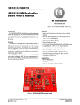
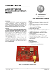
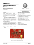
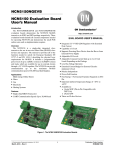
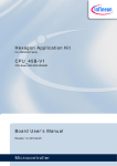
NCN5192NGEVB
NCN5192NG Evaluation
Board User's Manual
http://onsemi.com
EVAL BOARD USER’S MANUAL
Introduction
Features
• Single-chip, Half-duplex 1200 bits per Second FSK
The NCN5192NGEVB includes all external components
needed for operating NCN5192 and demonstrates the small
PCB surface area such an implementation requires. The
EVB allows easy design of HART implementations using
NCN5192.
•
•
•
•
•
•
•
•
•
•
•
Overview
The NCN5192 is a single-chip, CMOS modem for use in
highway addressable remote transducer (HART) field
instruments and masters. The modem and a few external
passive components provide all of the functions needed to
satisfy HART physical layer requirements including
modulation, demodulation, receive filtering, carrier detect,
and transmit-signal shaping.
The NCN5192 also includes an internal 16-bit
sigma-delta modulation DAC for easy implementation of
slave devices. An SPI bus provides easy communication to
this DAC and internal registers.
Modem
Bell 202 Shift Frequencies of 1200 Hz and 2200 Hz
3.0 V − 5.5 V Power Supply
Transmit-signal Wave Shaping
Receive Band-pass Filter
Low Power: Optimal for Intrinsically Safe Applications
Compatible with 3.3 V or 5 V Microcontroller
Internal Oscillator with 1.84 MHz Crystal
Meets HART Physical Layer Requirements
Includes 16-bit DAC for Slave Implementation
Industrial Temperature Range of −40°C to +85°C
Available in 32-pin QFN
Applications
• HART Multiplexers
• HART Modem Interfaces
• 4-20 mA Loop Powered Transmitters
Figure 1. NCN5192NGEVB Evaluation Board
© Semiconductor Components Industries, LLC, 2012
October, 2012 − Rev. 4
1
Publication Order Number:
EVBUM2047/D
NCN5192NGEVB
Table 1. ELECTRICAL CHARACTERISTICS OF THE NCN5192NGEVB BOARD
Symbol
VDD
Characteristic
Supply Voltage
Min
Typ
Max
Units
2.80
3.00
6.00
V
Current Consumption
IDD
VDD = 2.80 V, idle
−
350
−
mA
IDD
VDD = 3.00 V, idle
−
360
−
mA
IDD
VDD = 6.00 V, idle
−
490
−
mA
IDD
External Clock, VDD = 3.00 V, idle
−
290
−
mA
IDD
External Clock, VDD = 2.80 V, idle
−
240
−
mA
Transmitted Frequency
fM
Mark “1”
−
1194
−
Hz
fS
Space “0”
−
2204
−
Hz
VTxA
Amplitude Transmit Output
−
500
−
mV p-p
VCD
Carrier Detect Level
−
110
−
mV p-p
Levels
Reference Voltages
VAREF
AREF
−
1.248
−
V
VCDREF
CDREF
−
1.163
−
V
NCN5192 Description
Test and Measurement Tools
The NCN5192 modem is a single-chip CMOS modem for
use in HART field instruments and masters. It includes
on-chip oscillator and a modulator and demodulator module
communicating with a UART without internal buffer, as
well as an internal 16 bit sigma delta DAC. The NCN5192
requires some external filter components and a 460.8 kHz,
921.6 kHz, or 1.84 MHz clock source. This clock source can
either be the interface oscillator by using a crystal or ceramic
resonator, or an external clock signal.
When the device is transmitting data, the receive module
is shut down and vice versa to conserve power. With simple
power-saving maneuvers, the IC can be made to operate
with a current consumption of as little as 250 mA. The same
techniques apply as explained for the A5191HRT in the
Design Note “A5191HRT Design for Low-Power
Environments” (AND9030/D).
Listed below are the tools used to acquire the values
presented in this evaluation board.
• Oscilloscope: Tektronix DPO4101 1 GHz
• Signal Generator: Agilent 33250A
http://onsemi.com
2
NCN5192NGEVB
NCN5192NGEVB DESCRIPTION
Schematic Diagram − BOM List
Figure 2. NCN5192NGEVB Schematic
http://onsemi.com
3
NCN5192NGEVB
Table 2. NCN5192NGEVB BILL OF MATERIALS
Reference
Manufacturer & Comments
Value
Size
Quantity
C1, C2, C3, C7, C8
100 nF
0603
5
C4, C5
27 pF
0603
2
C6, C14, C15
C9
C10, C11
C12
C13
Do Not Populate
IDC1, IDC2, IDC3, IDC4
1 mF
0603
3
470 nF
0603
1
1 nF
0603
2
220 pF
0603
1
DNP
0603
1
IDC10
J2
SMB Connector, Do Not Populate
R12, R14, R20, R24, R38, R40
Do Not Populate
R13, R21, R22, R23, R30, R31, R36
R15, R39
4
DNP
0603
1
DNP
0603
6
220 kW
0603
7
0R
0603
2
R25
560 kW
0603
1
R26, R27, R28, R32, R35
470 kW
0603
5
R29
33 kW
0603
1
R33
680 kW
0603
1
R34
3M3
0603
1
4k7
0603
1
R37
TP5, TP6, TP7, TP8
Do Not Populate
DNP
4
U1
ON Semiconductor
NCN5192
1
U2
Linear Technology
LT1790−1.25
1
Y1
TOKEN
ZTACC1.84MG
1
General Overview
The NCN5192NGEVB evaluation board demonstrates
the external components required for the operation of the IC.
We will cover the different sections below as well as possible
alternatives. A drawing of the board where the different
sections are indicated is shown below.
Figure 3. Board Drawing with Indication of Different Sections
http://onsemi.com
4
NCN5192NGEVB
Power Supply and References
Power Supply
Current consumption of the module is very limited,
making it ideal to be battery or loop-powered.
Measurements of the power consumption of the module are
listed in Table 1.
The module will use less power when clock signal is
applied externally, as this allows the modem to shut down
the oscillator circuit. As is to be expected, a higher supply
voltage increases current consumption.
The NCN5192 includes an internal voltage supervisor.
This will guarantee correct operation of the digital circuitry
during start-up. All that is required for using this supervisor
is an external resistor divider (R25, R26). The voltage
supervisor compares the voltage offered by the resistor
divider on the VPOR pin to AREF. The resistor divider
should be dimensioned such that at the desired turn-on point
of the voltage supervisor, the VPOR pin is equal to AREF.
On the evaluation board the resistor divider is dimensioned
to make the POR trip at 2.8 V.
The voltage supervisor will keep the RESETB pin low
until its threshold value is reached, and will then wait an
additional minimum of 35 ms until it releases the RESETB.
This ensures that some time has passed after the supply
voltage reaches the turn-on voltage.
The RESETB en VDD pin signals during startup are
shown in Figure 5. The measured start-up delay is 48 ms.
The NCN5192NGEVB is designed for a nominal voltage
of 3 V. However, NCN5192 can be operated up to 6 V. For
optimal functioning of the board, the values of several
resistors should be changed for operation at voltages higher
than 3 V (see the sections on reference voltages and bias for
more information).
Figure 4. Supply Voltage and Power on Reset
Figure 5. Power (Light Blue) and RESETB (Dark Blue) Waveform during Startup, Showing 48 ms Startup Delay
http://onsemi.com
5
NCN5192NGEVB
regulator is more desirable from a power usage perspective,
as a series regulator’s current draw will vary with the output
current, whereas a shunt regulator is dimensioned on the
maximum current draw and will always draw the same
current. Large capacitors on the in- and output of the voltage
regulator increase the reference stability.
The CDREF reference voltage sets the threshold for the
carrier detect comparator. As the received signal is biased at
AREF, the difference between CDREF and AREF will
determine the minimum amplitude needed for the carrier
detect comparator to flip. A (AREF-CDREF) of 80 mV
corresponds to signal of approximately 100 mV
peak-to-peak at the input of the receive filter. The CDREF
reference voltage on the NCN5192NGEVB is generated by
a resistor division of the AREF reference.
An external resistor is required to set the bias current. The
voltage over the bias resistor is regulated to AREF, so that
the resistor determines a bias current. This bias current
controls the operating parameters of the internal operational
amplifiers and comparators and should be set to
approximately 2.5 mA. For low cost solutions, a 470 kW is
acceptable with minimal effect on operation.
C2, C3 and C14 are 100 nF ceramic decoupling capacitors
located directly adjacent to each power pin. For analog
power pins, an additional large-value ceramic capacitor may
be needed in addition to the 100 nF decoupling capacitor
when the application is intended for high-noise
environments.
For loop-powered devices, additional decoupling with a
large value capacitor is advised to prevent digital noise from
being transmitted on the current loop.
Additional ferrite beads in series with power supply lines
can help to reduce EMI.
Reference Voltages and Comparator Bias
NCN5192 needs an external analog reference voltage.
This reference is used by receiver or demodulator (RX)
comparator, carrier detect (CD), and voltage supervisor.
The AREF reference voltage sets the trip point of the
demodulation operational amplifier of the NCP5192. The
AREF reference voltage is also used in setting the DC
operating point of the received signal after it has passed
through the band-pass receive filter. The ideal value for the
AREF reference voltage depends on the voltage supply, and
is chosen roughly half-way the operating range of the
operational amplifiers. This ensures the range of the
operational amplifier is maximized. For operation at 3 V, a
1.24 V reference voltage is recommended. For operation at
5 V, a 2.5 V reference voltage is recommended.
For NCN5192NGEVB, a series regulator is used with an
internal reference of 1.25 V. The chosen regulator has a very
low supply current, to optimize power usage. Using a series
Table 3. REFERENCE VOLTAGES
Description
AREF Reference Voltage
1.248 V
CDREF Reference Voltage
1.163 V
Figure 6. Reference Voltages Schematic
http://onsemi.com
6
Value
NCN5192NGEVB
Clock Generation
modem to shut down the oscillator circuit. A typical current
consumption witnessed by utilizing an external oscillator is
70-100 mA less. However, care must be taken that this
external signal has the required frequency accuracy (1%).
Duty cycle of the clock signal is specified between 40%
and 60%. No errors were observed during testing in
operation between 20% and 80% duty cycle. However,
operation on such very small or very large duty cycle is not
recommended, due to the possibility of timing errors that
may occur under specific circumstances (including, but not
limited to, temperature variations).
NCN5192 is operated on a clock signal of either
460.8 kHz, 921.6 kHz or 1.84 MHz. The NCN5192NGEVB
has two options for providing this clock signal. The first
method is by using a ceramic resonator or a crystal with the
internal oscillator. The standard populated option is a Token
ZTACC1.84MG ceramic resonator, loaded with two 27 pF
capacitors.
Alternatively, a clock signal can be provided externally
when R37 is removed and R24 is populated by a resistor of
0 W. This signal can be provided by a microcontroller or any
other external oscillator circuit. The module uses less power
when clock signal is applied externally, as this allows the
Figure 7. Clock Generation Circuit
(Resonator Option)
Figure 8. Clock Generation Circuit
(External Clock)
UART Interface IDC1
Figure 9. UART Interface (IDC1)
Table 4. MICROCONTROLLER INTERFACE
Pin Number
Signal
Type
Description
1
RESETB
Open Drain
Reset Signal from the Voltage Supervisor, Open Drain with Pull-up, Active Low
3
CD
Output
5
RxD
Input
7
TxD
Output
Carrier Detect
Receive from Microcontroller
Transmit towards Microcontroller
9
RTSB
Input
2, 10
VDD
Power
Request to Send, Active Low
3 V Nominal
4, 6, 8
GND
Power
Ground
http://onsemi.com
7
NCN5192NGEVB
time base in another device is at 101% of nominal, the
receive data (at the receiving UART) will be skewed by
roughly 21% of one bit time at the end of each 11-bit byte.
This is shown in Figure 10. The skew time is measured from
the initial falling edge of the start bit to the center of the 11th
bit cell. This 21% skew by itself is a relatively good result.
However, there is another error source for bit boundary jitter.
The Phase Lock Loop demodulator in the NCN5192
produces jitter in the receive data that can be as large as 12%
of a bit time. Therefore, a bit boundary can be shifted by as
much as 24% of a bit time relative to its ideal location based
on the start-bit transition. (The start-bit transition and a later
transition can be shifted in opposite directions for a total of
24%).
The clock skew and jitter added together is 45%, which is
the amount that a bit boundary could be shifted from its
expected position. UARTs that sample at mid-bit will not be
affected. However, there are UARTs that take multiple
samples during each bit to try to improve on error
performance. These UARTs may not be satisfactory,
depending on how close the samples are to each other, and
how samples are interpreted. A UART that takes a majority
vote of 3 samples is acceptable.
Even if your own time base is perfect, you still must plan
on a possible 35% shift in a bit boundary, since you don’t
have control over time bases in other HART devices.
The interface towards a microcontroller is provided in
IDC1. This interface can also be used to supply power to the
module. The nominal supply voltage for the module is 3 V.
For more information see the section on power supply and
references.
The RESETB line to the modem is an open drain signal.
A pull-up resistor of 200 kW is provided on the board, and
should not be duplicated on the microcontroller side. The
reset signal is generated on the board, and could be used as
reset signal for other IC such as the microcontroller.
The CD signal rises when a HART signal of ca. 100 mVpp
is detected on the current loop. See the section on reference
voltages for more information on these threshold level
settings. When no signal, or a signal of limited amplitude is
present, the CD line is pulled down to 0 V.
The RxD, TxD, and RTSB signals implement a standard
UART interface at 1200 baud with start bit, 8 data bits, parity
bit and stop bit (11-bit frame). The RTSB signal disconnects
the transmitter circuit when pulled high, and should be held
low before any data is transmitted. Data frames are not
buffered by the modem. Instead, data is transmitted bit by
bit. Care should be taken to avoid clock skew in the receiving
UART. If the same time base is used for both the modem and
the UART, a 1% accurate time base may not be sufficient.
The problem is a combination of receive data jitter and clock
skew between transmitting and receiving HART devices. If
the transmit time base is at 99% of nominal and the receive
Figure 10. Clock Skew
SPI Interface and Internal Register
The NCN5192 also has an SPI interface that is used to
control the integrated DAC and set the configuration register
of the IC. This interface is accessible on the evaluation board
through connector IDC5.
The length of the SPI frame determines what the function
of the frame is. For setting the internal register, the SPI frame
has a length of 8 bits, containing all the bits of the internal
register. To set the output of the integrated DAC, a frame of
length 14 or 16 can be used, depending on which mode of the
DAC is used. For more information, see the section on the
integrated DAC.
Figure 11. SPI Interface (IDC5)
http://onsemi.com
8
NCN5192NGEVB
Table 5. SPI/DAC INTERFACE
Pin Number
Signal
Type
Description
5
DAC
Output
DAC Output
4
CLK
Input
SPI Clock
6
DATA
Input
SPI Data in (MOSI)
8
CS
Input
SPI Chip Select
1, 2, 3, 7, 9, 10
GND
Power
wave shaping and activating the internal watchdog kick.
Depending on your application, other bits may need to be set
as well. See the description of the internal register in de The
NCP5192 datasheet for more information.
At reset of the device, all bits of the internal register are set
to 0. This means that, before being able to use the evaluation
board, an SPI frame must first be sent to configure the
device. This frame must set bit 1 and bit 5 to one, setting
respectively the correct frequency division factor for the
Internal Sigma-Delta DAC
The included DAC has a Sigma-Delta topology. This
means that the output of the DAC is constantly switching
between 0 V en DACREF (3 V on the evaluation board). To
achieve optimum accuracy, it is required that DACREF is
sufficiently decoupled from the power supply, such as by a
large-value ceramic capacitor (1 mF typical).
The switching output signal will have the desired DC (low
frequency) component, but also includes a lot of switching
noise that needs to be filtered out before the signal is useful.
Figure 13 shows a typical frequency spectrum of the output
of the DAC. This means that an output low pass filter is
required before the DAC output can be used. Since the
sigma-delta modulator is designed for a bandwidth of 10 Hz,
it is advised that the corner frequency of the output filter is
placed on this frequency.
For more information on how to design this filter, see the
section on slave implementation.
Figure 12. DAC Interface
The NCN5192 includes an internal DAC that can be used
for the implementation of a slave analog transmitter.
Figure 13. DAC Output Spectrum (code 32768, 16 bits non-RTZ)
http://onsemi.com
9
NCN5192NGEVB
However, operating the DAC in RTZ mode limits the
operational range of the DAC to half of the voltage applied
to the DACREF pin. By setting the DAC to non-RTZ
(setting bit 6 of the internal register), a larger output range
is achieved, but at the cost of accuracy. In non-RTZ mode,
16-bit accuracy will be harder to obtain.
To achieve maximum accuracy of the DAC, it is also
advised to use a separate, low-noise reference as DACREF
instead of tying this pin to VDD, and to keep the DAC line
away from noisy signal lines.
By default the DAC is set to 14-bit, RTZ (return to zero)
mode. The DAC can be set to either RTZ or non-RTZ mode.
This is important when rise and fall times are not identical.
This will cause a DC offset depending on the number of
rising and falling edges. As the output bits of a sigma-delta
modulator are randomly arranged, the number of edges
might vary widely in non-RTZ mode, which results in
reduced accuracy. Setting the DAC to RTZ mode forces the
modulator to have a rising and falling edge on each logic “1”
bit, so that no offset from pulse asymmetry can occur.
Transmitter
waveform shown in figures 12 and 13. This pin can only
drive impedances higher than 30 kW, and as a consequence
may need to be amplified.
The nominal frequency of the output is 1200 Hz for
“mark” and 2200 Hz for “space”. These frequencies are
dependent on the accuracy of the NCN5192 clock.
The TxA modem pin is accessible through pin 7 of IDC2.
For certain applications, it might be required to couple the
transmit signal in the circuit by adding a series capacitor.
Note that this is a difference with the A5191HRTNEVB,
where this coupling capacitor was provided on the board.
The output on this pin is a 500 mVpp signal trapezoid
Figure 14. Output Waveform (Mark)
http://onsemi.com
10
NCN5192NGEVB
Figure 15. Output Waveform (Space)
Receiver
The receive band pass filter is implemented on the
NCN5192NGEVB. The values are listed in Table 6 and the
filter schematic is displayed in Figure 16. This is a band pass
filter based on a Sallen-Key topology allowing only
frequencies around the HART signal frequencies to pass
through. For a more detailed description of the filter see the
user manual of A5191HRTNEVB.
Table 6. RECEIVE FILTER COMPONENT VALUES
Reference
Value E12 (Low-cost)
R30, R31, R36
220 kW, 1%
R32, R35
470 kW, 1%
Figure 16. Receive Filter
http://onsemi.com
11
R33
680 kW, 1%
R34
3.3 MW, 1%
C9
470 pF, 5%
C10, C11
1 nF, 5%
C7
220 pF, 5%
NCN5192NGEVB
APPLICATION IDEAS
The NCN5192 takes care of the HART modulation. This
HART signal must then be superimposed on a 4-20 mA
current loop. The NCN5192 simplifies slave implementation
by including an integrated DAC. Below are some possible
implementations of both a master and slave transmitter.
Slave Implementation
A simple slave implementation is shown in Figure 18. The
analog loop current is set by the integrated DAC, and HART
signals are added to this by a resistive summing network.
The DAC is implemented as a sigma-delta modulator, which
means that additional filtering should be implemented. To
explain the operation of this circuit, let us first look at an
example where the DAC is not of a switching topology, such
as shown in Figure 17. As one end of R6 is tied to local
ground, and current passing through R7 also passes through
R6, it can easily be seen that the voltage at the negative loop
terminal is negative with respect to the local ground.
Resistor R4 is then chosen so that in steady state their
common terminal is a virtual ground point in the absence of
HART signals, since the negative terminal of the amplifier
is also connected to ground. A similar principle applies
when HART signals are applied. So both amplifier inputs are
regulated to ground.
Figure 17. Simple Slave Implementation
A compensation capacitor C4 may be required depending
on the operational amplifier used. To avoid offset generated
by bias current in the operational amplifier, a resistor R3
should be placed on the negative input, and dimensioned to
approach the impedance seen by the positive terminal.
The amplifier will then determine the current flowing
through the loop by changing the base of a transistor in
emitter feedback configuration. The value for R7 is
determined by the output range Vo,max of the amplifier used:
R 7, max +
Where:
Z+
ŤsC1 ) R Ť
1
1
In practice, C1 is chosen sufficiently large so that Z ≈ R1.
Because the integrated DAC has a sigma-delta output, a
circuit using the NCP5192 gets a bit more complicated, as
can be seen in Figure 18. We need to filter away high
frequency DAC components, but leave HART signals intact.
A simple RC-filter is not sufficient, since the output
capacitor has low impedance for HART frequencies. We can
do this by replacing the summing resistor R4 by a T-filter.
This filter has high output impedance due to the output
resistor.
To dimension this filter without too much calculation, we
can treat it as a RC-filter using its first branch. The 3-dB
frequency should be placed just above the DAC bandwidth
(10 Hz).
We get, with R4 ≈ R5:
V o, max * V BE
20 mA
It is often recommended to take a value as large as
possible, so that noise effects are minimal.
Typically the value of R6 is chosen equal to R7. The
voltage over R6 and R7 combined should however be less
than 12 V when the current setting is 20 mA.
Next, the value of R4 is chosen depending on the most
significant bit of the DAC.
2 V MSB R 2 + 20 mA R 6 R 4
f 3dB +
When the DAC is not a switching topology, we can now
choose R1 and C1. We have:
1
2p C 3 R 4
To dimension the summing resistor of the HART input, we
can no longer assume that the positive input of the amplifier
500 mV R 2 + 1 mA R 6 Z
http://onsemi.com
12
NCN5192NGEVB
is a virtual ground, as this assumption is only valid for DC
signals. We can, however, find a relationship between input
amplitude and output amplitude. We know that the positive
amplifier input voltage has the following form, due to the
summing network:
V ) + ǒR 1ńńR 2ńńǒR 4 ) R 5ǓǓ
V out +
Reconfiguring for the unknown R1:
R1 +
ǒVR * VR Ǔ
in
out
1
2
ǒR 1ńńR 2ńńǒR 4 ) R 5ǓǓ
R2
V
R 1 ǒR 1ńńR 2ńńǒR 4 ) R 5ǓǓ ) R 2 in
R 2ǒR 4 ) R 5ǓV in ) V outǒR 2 ) R 3Ǔ
V outǒ1 ) ǒR 4 ) R 5ǓǓ
The amplifier is configured as an integrator for low
frequencies. Care must be taken that the 3-dB frequency of
the integrator is below the HART band, so that the amplifier
gain in that band is independent of frequency. The resistor
R3 is chosen so that it compensates for input bias current.
This is achieved by taking a value close to the resistance seen
on the positive terminal. This means that the capacitor C2
needs to be chosen so that (2 p R3C2)−1 < 1 kHz.
The amplifier is configured as an integrator for low
frequencies, but for high frequencies, the amplifier
configuration has a gain of 1, and the transistor is configured
as a voltage follower, so we can conclude that for AC
frequencies V+ = Vout. Taking this into account, we get the
following equation:
Figure 18. Sample Slave Implementation
Master Implementation
An example of a possible master implementation is shown
in Figure 19.
The current loop master has a sense resistor over which the
current flowing through the loop can be measured. The value
of this resistor varies depending on the sensitivity required
and range of the ADC. A HART Master can have a sense
resistor ranging from 230 W to 600 W. Increasing the sense
resistor will result in higher amplitude HART signal
received, but will also reduce the voltage available on the
slave side. Furthermore, if you wish to sense the analog
transmitted signal, the MSB of your DAC may limit the
resistor size. If this limitation is too stringent, the sense
resistor can be split in two resistors, as shown in the figure,
effectively creating a resistor divider.
To transmit a HART signal, the TxA signal will need to be
amplified, as the NCN5192 transmit circuit can only drive
high impedance circuits (>30 kW). An additional
operational amplifier is required. Depending on the sense
resistor used, some gain or attenuation may be required to
get a 1 mA peak-to-peak HART output signal. This can be
accomplished by the resistors R3 and R4. For a typical sense
resistor of 500 W, a unity gain suffices and a unity gain
operational amplifier configuration can be used instead.
The amplifier however has a low impedance output,
which cannot be paralleled with the sense resistor, as this
would cause problems when the slave is transmitting. This
problem is solved by adding a series switch (such as
MC74VHC1G66DTT1G), controlled by the RTS signal.
For a normally open switch, the nRTS signal as applied to the
NCN5192 must be inverted first. To reduce power usage, the
operational amplifier can be disabled when the transmitter
is turned off. This is both done by inserting PNP transistor
Q1on the VDD connection of the amplifier.
To couple the signal into the current loop, a single
capacitor was used. For other coupling techniques see
application note AND8346/D.
http://onsemi.com
13
NCN5192NGEVB
Figure 19. Sample Master Implementation
http://onsemi.com
14
NCN5192NGEVB
APPENDIX
Evaluation Board Layout
Figure 20. Top Layer Layout
Figure 21. Bottom Layer Layout
ON Semiconductor and
are registered trademarks of Semiconductor Components Industries, LLC (SCILLC). SCILLC owns the rights to a number of patents, trademarks,
copyrights, trade secrets, and other intellectual property. A listing of SCILLC’s product/patent coverage may be accessed at www.onsemi.com/site/pdf/Patent−Marking.pdf. SCILLC
reserves the right to make changes without further notice to any products herein. SCILLC makes no warranty, representation or guarantee regarding the suitability of its products for any
particular purpose, nor does SCILLC assume any liability arising out of the application or use of any product or circuit, and specifically disclaims any and all liability, including without
limitation special, consequential or incidental damages. “Typical” parameters which may be provided in SCILLC data sheets and/or specifications can and do vary in different applications
and actual performance may vary over time. All operating parameters, including “Typicals” must be validated for each customer application by customer’s technical experts. SCILLC
does not convey any license under its patent rights nor the rights of others. SCILLC products are not designed, intended, or authorized for use as components in systems intended for
surgical implant into the body, or other applications intended to support or sustain life, or for any other application in which the failure of the SCILLC product could create a situation where
personal injury or death may occur. Should Buyer purchase or use SCILLC products for any such unintended or unauthorized application, Buyer shall indemnify and hold SCILLC and
its officers, employees, subsidiaries, affiliates, and distributors harmless against all claims, costs, damages, and expenses, and reasonable attorney fees arising out of, directly or indirectly,
any claim of personal injury or death associated with such unintended or unauthorized use, even if such claim alleges that SCILLC was negligent regarding the design or manufacture
of the part. SCILLC is an Equal Opportunity/Affirmative Action Employer. This literature is subject to all applicable copyright laws and is not for resale in any manner.
PUBLICATION ORDERING INFORMATION
LITERATURE FULFILLMENT:
Literature Distribution Center for ON Semiconductor
P.O. Box 5163, Denver, Colorado 80217 USA
Phone: 303−675−2175 or 800−344−3860 Toll Free USA/Canada
Fax: 303−675−2176 or 800−344−3867 Toll Free USA/Canada
Email: [email protected]
N. American Technical Support: 800−282−9855 Toll Free
USA/Canada
Europe, Middle East and Africa Technical Support:
Phone: 421 33 790 2910
Japan Customer Focus Center
Phone: 81−3−5817−1050
http://onsemi.com
15
ON Semiconductor Website: www.onsemi.com
Order Literature: http://www.onsemi.com/orderlit
For additional information, please contact your local
Sales Representative
EVBUM2047/D