1
e,.:.
-.
.
.
Carnegie-Mellon University
RAPIDbus
Architecture and Realization
John C willis
Dr. Arthur C. Sanderson
The Robotics Institute
Carnegie-Mellon University
Pittgburgh, Pennsylvania 15213
I
CMU-RI-TR-82-13
ROBOTICS
INSTITUTE
RAPlDbus
Architecture and Realization
Abstract
R APIDbus: Architecture and Realization describes a synchronous multiprocessor designed IOsapport sensory
processing, image understanding, and control applications. Up to eight board level rnastcrs jntcract with up
to eight slaves along a time-multiplexed implementation of a crossbar switch. Two implementations arc
considered, one based on an Advanced Shottky logic with a bus bandwidth of.16 Mh7 and a Vcrsabus host
interface. The second implementation, based on an ECL/'TTL gate array, permits an estimated 64 Mhz of bus
bandwidth and a Versabus/Multibus host interface. Segmented memory managesent. a tnulticzst capability
between one master and niultiple destinations, and a standardized host interface aid in making K;\PIDbus an
appropriate architecture for robotic applications.
John C.Willis
Dr. Arthur C.Sanderson
The Robotics Institute
Carnegie-Mellon University
Pittsburgh, Pennsylvania 15213
November 1982
This research was support by the National Science Foundation under grant number ECS-7923893.
RAPIIlbus: Architecture and Realization
i
Table of Contents
1. Overview of RAPlDbus Specification
1.1 What is RAPIDbus?
1.2 System Elements
2. Summary of Versabus Specifications
2.1 Why the Versabus?
2.2 Versabus Protocol Summary
2.2.1 Data Transfer
2.2.2 Bus Arbitration
2.2.3 Interrupt Handling
2.3 Versabus System Modifications
3. RAPlDbus Data Transfer Protocols
3.1 The Window Structure
3.2 Functional Modules
3.3 Reading and Writing on the Bus
3.3.1 Read Operations
3.3.2 Write
3.4 Multicast Capability
3.5 Definition of Signal Lines for Data Transfer
3.5.1 Time-multiplexed Signal Lines
3.5.2 Non-Multiplexed Bus Signals
4. The Address System
4.1 Address Trarlslation
4.1.1 Partitioning of Memory
4.1.2 Functional Description
4.1.3 Internal Register Manipulation
4.1.4 System Performance Considerations
4.2 Inteiface Control Register
4.2.1 Interface Control Register Upper Byte
4.2.2 Interface Control Register Lower Byte
4.3 KAPIDbus Physical Memory Map
2
2
6
8
8
9
9
10
11
12
13
13
14
18
18
19
20
23
23
25
28
28
28
30
30
35
36
37
39
41
5. The Priority Interrupt System
53
5.1 Interrupt System Objectives
5.2 Functional Modules
5.3 Interrupt Service Protocol
53
53
54
6. lbus Arbitration and Control
57
6.1 Use of the Ibus and Virtual Buses
6.2 Master Ibus Access
6.3 Memory Access
6.4 Multicast Access
6.5 Interrupt Vector
6.6 Ibus Operation Summary
7. System Support
57
58
62
63
64
66
67
4
RAPIDbus: Architecture and Realization
7.1 System Timing
7.1.1 The Master Clock
7.1.2 ‘The Window Address System
7.1.3 The Host Clocks
7.2 Control Lines
7.2.1ACCLK
7.2.2 Reset
7.2.3 Test Configuration Lines
7.2.4ACFAIL
.
7.3 110 Interface
7.3.1 I/O Bus
7.3.2 Serial Access
ii
67
67
69
70
71
71
71
72
72
72
73
74
8. Where Next?
77
1. Connector CP1 Signals
78
II. Connector CP2 Signals
80
RAPIDbus: Architecture and Realization
...
111
List of Figures
Figure 1-1: The interconnection scheme for a multiprocessor system can have a heavy effect on
system efficiency.
Figure 1-2: Common bus architectures trade off simple hardware for increased bus contention in a
multiprocessor system.
Figure 1-3: Multiport Memory reqiires a unique link between each processor and one or more
system memory arrays.
Figure 1-4: Crossbar switching permits multiple connections between processor and memory to be
made randomly and simultaneously. but requires complex hardware.
Figure 1-5: A time multiplexed common bus structure allows multiple simultaneous random paths
with a switching circuit that grows in switch bandwidth and not N4 switch complexity as
does a crossbar switch.
Figure 1-6: A Rapidbus system is composed of many independent elements.
Figure 3-1: The virtual bus system is implemented using bus windows to link several masters and
several slaves simultaneously
Figure 3-2: Each RAPIDbus interface card is composed of multiple modules, centered around the
Ibus.
Figure 3-3: Several multicast address generawrs are needed to create the full address range
required for a memory access. A single module is shown here. This illustration is
adapted from Advanced Micro lkvices data sheet on the AMD 29401j
Figure 4-1: The MC68451 memory management unit supports address trznslation and memory
protection.
Figure 4-2: The address space tables links the incoming hnction code and memory map bit from
the control register with the cycle address space number16.
Figure 4-3: The 32 descriptor arrays each define a translation process. The system registers select
the descriptor array that is to be used during this data transfer cycle16.
Figure 4-4: Each processor sees the memory management unit registers assigned to that unit in the
Same address locations16.
Figure 4-5: Continuation of the memory manzigenient unit address map16.
Figure 4-6: The descriptor pointer selects the descriptor array that is used in a load descriptor
operation, read segment status, and the write segment status operation16
Figure 4-7: The Global Status Re 'ster summarizes the faults that have occurred and the interrupt
levels that are enabled
Figure 4-8: The I d Status Register indicates the status of write* when a fault occurs, the
consistency of the descriptm, and an indication of the. highest priority intempt
pending16
Figure 4-9: The segment status register is selaxed through the Descriptor Pointer register indirectly
E
16
Figure 4-10: The interrupt descriptor ointer indicates which descriptor array was in use when an
interrupt was generatedl?.
Figure 4-11: The Result Descriptor Pointer identifies the descri tor involved in a write violation,
load descriptor failure, or direct translation successli?.
Figure 4-12: Interface control register low byte
Figure 4-13: Interface control register high byte
Figure 4-14: Lower RAM supervisor space
Figure 4-15: User RAM and upper supervisor space
Figure 4-16: Upper RAM supervisor space, ROM, and Timers
Figure 4-17: Versamodule registers, and master interface control page
2
3
3
4
4
7
14
15
21
29
31
32
33
34
35
36
37
38
38
39
40
41
42
43
44
45
RAPIDbus: Architecturc and Kealization
Figure 4-18: Master interface control page
Figure 4-19: Master interface control pagc [MMU]
Figure 4-20: Slave .#1 and Slave # 2 intcrface control pages
Figure 4-21: Slave # 3 and Slave #4 intcrface control page
Figure 4-22: Slave # 5 and Slave #6 interface control page
Figure 4-23: Slave # 7 and Slave # 8 interface control page
Figure 4-24: 110 and RAPlDbus address space
Figure 6-1: A data transfer begins with a master access.
Figure 6-2: Control page references are used to modify the RAPIDbus interface configuration or
that of the memory managerncnt unit assigned to the processor’s virtual bus.
Figure 6-3: The memory reference access to the host allows host processors to examine and modify
memory locations on the host
Figure6-4: ‘ h e multicast reference to this host allows multiple locations to be written into
simultaneously
Figure 6-5: ’The interrupt handler cycle allows the interrupting Versabus host to tell the interrupt
handler which service routine to choose to service the interrupt.
Figure 7-1: All synchronous system timing is derived from a single time base
Figure 7-2: An eight processor system requires either a high bandwidth backplane or a low
frequency processor clock
Figure 7-3: A four processor system can reasonably be implemented in Advanced Schottky ‘ITL to
support eight MHz processor clocks
Figure 7-4: The front panel processor simplifies interactions with multiple proccssors.
iv
46
47
48
49
50
51
52
59
61
62
64
65
67
69
70
75
KAPIDbus: Architecture and Realization
1
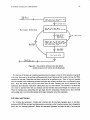
The concept of a Rotary Access, Parallel Implementing, Digital bus (RAPIDbus) was first proposed as an
ECL machine by Zoccoli and Sanderson [l]. Bracho [2] suggested the creation of a 7 T L machine making use
of a time-multiplexed Versabus convention. The adaptation of the Versabus convention as the host interface
makes available a wide variety of commercial processors, memory systems, and peripheral processors.
This specification defines an architecture and realization of a RAYIDbus system based on a series of virtual
Versabuses. Motorola has described the Versabus architecture [3] in a rigorously defined specification. Thus
it is the primary intent of this document to describe the RAPIDbus as an interconnect system for a series of
host ports obeying the Versabus convention. Beyond assuming the Versabus convention at the host ports,
charscteristics of the Versabus hosts such as the presence of a processor and memory mapped to the host port
must be known in the configuration of the interface card. Thus tremendous flexibility is made available in the
actual processors and resources that RAPIDbus supports.
Prospective users of the RAPIDbus prototype system at Carnegie-Mellon will find sections of this
document to be relevant in evaluating the suitability and formulating use of the machine for their
applications. Those interested in exploring the different interconnection schemes available for multiple
pairings of processors and system resources may find the time-multiplexed switching used here to be relevant
to the realization of other architectures.
T w companion reports are in preparation. The first describes an implementation of the RAPIDbus
architcccurc in Advanced Shottky logic, supporting four 8 MHz processors. The Shottky report includes
circuit diagranis and a detailed discussion of one possible implementation schema. A performance analysis of
?he Advanced Shottky implementation and its impact on a higher performance ECL logic version of the
RAPIDbiis architecture is briefly proposed in the second report. Initial review suggests the ECL version,
based on TTL/ECL gate arrays, would be capable of supporting eight processors running at clock speeds
approaching 16 MHz. This second version may also allow interfacing Multibus cards at the host interface
level along with \'ersabus hosts.
Credit for this project is due to a great many people who have contributed heavily. Dr. Arthur Sanderson
and Mario Zoccoli first proposed a time-multiplexed backplane. Rafael Bracho suggested the use of a
Versabus interface to the host and the use of Advanced Shottky as an implementation technology. Dario
Giusc heavily supported the graphics and computer aided design system (Drawing Package) [4]. Construction
support for the advanced Shottky implementation is being provided by the Computer Science Engineering
Laboratory at Carnegie- Mellon University, and Dave Coleman. This research was made possible in part by a
grant from the National Science Foundation number ECS-7923893.
2
RAPIDbus: Architccture and Realization
1. Overview of RAPlDbus Specification
1.1 What is RAPIDbus?
RAPIDbus is a multiprocessor architecture aimed at effectively supporting signal processing, task
integration, display, and control algorithms in 3 real time research environment. Such applications are
characterized by a high bandwidth of interprocessor communications. As the size of a system increases, the
bandwidth available to connect processors and memory can become a system bottleneck, reducing the rate at
which additional system resources increase system rhroughput. For a multiprocessor system with several
processors and a variety of system resources, thc interconnection scheme can be an important parameter in
determining the efficiency with which multiple processors communicate.
Memory
A
Memory
B
Memory
C
Multiple P a t h
i n t e r c o n n e c t Sys tern Needed
1Memory'
Processor
1
Processor
2
Processor
3
Processor
4
-
Figure 1-1: The interconnxtion scheme for a multiprocessor system
can have a heavy effect on system efficiency.
Many current minicomputer.systems mzke use of a common bus architecture such as the Multibus, Qbus,
and Versabus protocols. Most common bus multiprocessor architectures resolve bus contention by assigning
the bus to one processor-memory pair for the duration of the memory access cycle. Other processors needing
the bus are required to wait until the existing request is serviced before obtaining bus mastership. Bus
intensive applications can' be subjected to a heavy performance penalty due to bus contention.
Both crossbar switching and multiport memorj configurations reduce contention, but at an increase in the
complexity level and a decrease in the expandability. Crossbar switching dedicates a switch for each signal
line and each combination of processor and memory. Systems such as C.mmp have shown that up to sixteen
processors and sixteen memory arrays can be connected reliably in this way, but the hardware cost and
complexity is non-trivial, increasing by the fourth power as new processors are added [SI,[6].
Multiporting provides several ports to one array of memory, depending on logic internal to the multiport
memory to arbitrate between requests, making their service seem simultaneous. A unique link between each
3
RAPlDbus: A r c h i t c c t w and Realization
Memory
A
Memory
B
Memory
C
I
I
Process0r
Processor
Processor
Processor
1
2
3
4
\/
\/
/\
/\
\/
/\
\/
/\
Figure 1-2: Common bus architectures trade off simple hardware
for increased bus contention in a multiprocessor system.
Processor
Processor
Local
Memory
Local
Memory
Processor
Local
Memory
Processor
Local
Memory
Figure 1-3: Multiport Memory requires a unique link between
each processor and one or more system memory arrays.
processor-memory pairing is required, leading to considerable interconnect complexity, and a lack of easy
expandability. The DEC MA-780, connecting up to four V A X 780s together is one example of a successhlly
executed multiport memory system [7].
RAPlDbus attempts to remove common bus contention by time-multiplexing the common bus, achieving
4
IIAPIIIbus: Architccturi and Redlization
rocessor
Figure 1-4: Crossbar switching permits multiple connections between
processor and memory to be made randomly and simultaneously, but
requires complex hardware.
the fkxibilicy for multiple pzths of the crossbar switch at a potential reduction in the hardware complexity. A
set of high s p e d drivers and latches attached to each RAPIDbus interface port provide a set of virtual buses,
one for each processor. A hie-multiplexed bus structure implements an increasing number of concurrent
paths nt)t by increasing the size of the switching mechanism, but by increasing the speed at which the latches
and drivers muitiplex, permitting more time slots pcr processor clock cycle.
-
I
I
V i r t u a l Bus c o n n e c t i o n s
as r e w i r e d .
(example shown)
Memory
B
-
I
I
m
m
a
Memory
C
c
D
r
0
0
-
r
=
0
-
L
2
Memory
I
m
P
>
5
*
0
t
c
m
w
r
0
- 2
5
Processor
Processor
Processor
Processor
1
2
3
4
Figure 1-5: A time multiplexed common bus structure allows
multiple simultaneous random paths with a switching
circuit that grows in switch bandwidth and not
N4switch complexity as does a crossbar switch.
RAPIDbus: Architeclure and Realization
5
The RAPIDbus architecture assigns a time-periodic window on the bus to each processor, designated by a
window address. Every time its window cycles around, each master interface card has the opportunity to
drive the physical RAPIDbus backplane. Comparators and latches on each of the slaves scan the address and
control lines, waiting to latch in a reference to their resources. When a slave interface recognizes a reference,
it is presented to the slave host, often a memory card. On subsequent occurrences of the master's window, the
slave's response is driven onto the RAPIDbus by tile slave interface card and latched in by the master
interface card initiating the request, terminating with the successful transmission of a single data word or a
transfer abort.
As defined in this specification, RAPIDbus provides a set of virtual buses for Versabus convention host
cards, memory management, multicast capabilit) , and interrupt handling. The interface serves to synchronize
and time-multiplex the asynchronous Versabus protocol. A variety of software configurations are possible,
simulating different interconnection schemes for research evaluation. Memory management is provided by
the RAPIDbus interface as an option for Versabus pacessor cards without memory management. A
multicast capability allows one processor at a time to scnd data words into multiple system memory locations
through previously prepared multicast address registers on each receiving card. Interrupt handling capability
allows any processor to be interrupted and an intempt vector to be requested explaining the reason for the
interrupt on the interrupt handler's virtual bus.
Some Versabus hosts with processors share 5 e same card and Versabus port with memory that is mapped
onto the system bus. Arbitration must occilr 50 that a given host resembles either a "processor" or a
"memory" for a single data transfer cycle. Thus when the memory on a processor card is being accessed, the
processor does not have access to its virtual bus and must wait until the memory access is completed. This
conflict is a result of the sharing of a Vcrsabus port by both system memory and a processor. In certain
applications separate processors and system menory cards may increase system throughput.
Commercially implemented examples of the bus window structure include the I'IT 1240 digital switch for
telephone switching [8],19] and the Digiiil Equipment Corporation bus window adapter for the PDP-11 [lo].
The I l T digital switch is intended to link between up to 100.000 lines using a hierarchical structure. Sixty
lines are controlled by a dedicated microproceswr which supports ringing, supervision, and digital encoding
for each line. Each microprocessor communicates through a terminal intcrface across one or more switching
planes to complete the required path between lines. The switching planes are each implemented using a bus
window circuit siinilar to that employed by RAPIDbus. The digital switch supports lower bandwidth links
than that intended for RAPIDbus, however a larger number of bus master6 are accommodated as a-result.
The DEC UNIBUS window adapter, the DA11-F, was marketed by DEC in the early 70's as an option for the
PDP-11 to link two processors. It allowed a window of up to 32k words to be mapped from the address space
of one processor to that of another processor. It appeared as a master on the target UNIBUS and a slave on
the originating UNIBUS. A series of DA11-F adapters allowed communication among several processors
[lo]. The UNIBUS window adapter differs from RAPlDbus primarily in that the RAPIDbus interface goes
between host and bus, the DA11-F linked among pairs of buses.
As a research project it is hoped that RhPIDbus will expand our understanding of processor-memory
interconnection dynamics. As a research tool RAPIDbus offers an interesting support medium for high
bandwidth interprocessor communication applications in robotics and signal processing applications.
R1ZPll)bus: Architecture and Realization
6
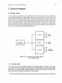
1.2 System Elements
The RAPIDbus architecture allows considerable flexibility the modules that are chosen to form a system,
such as that illustrated in figure 1-6. A minimal system has least two processors, two memory sections,
interface cards to support the processors and memory, a master clock controller card, and a backplane. A
system may have up to eight processors, depending on the implementation, an equal number of peripherals,
and RAPIDbus interface cards for all processors and peripherals. The advantages of the RAPIDbus virtual
buses are increasingly evident in terms of reduced common bus contention up to the implementation limit on
the number of processors.
Versabus pr&essor/memory hosts contain a processor capable of executing an instructicn stream and a
memory space which is accessible fiom the Versabus port. These cards can act as both masters, originating
memory references, and as slaves, acting as the target of memory references by other processors. The use of
the Versabus convention for thc parallel port between the processor and the rest of the system restricts the
card to act as either a master or a slave to the rest of the RAPIDbus while a single data transfer operation is in
progress. Processor/memory cards may support a local parallel 110 bus.
Versabus processor-only hosts incorporate a master capability. They must take data in and cutput data
using processor read and write operations. Like the processor/ memory cards, the processor-only cards may
support a local 110 bus.
A memory or I/O host can only function as a slave, completing data transfer operations that were initiated
by a system master. This class of host may include memory cards, display cards, or controllers for off-line
storage.
The interface cards are creatcd in a mother-daughter board configuration. acting s adapters between the
asynchronous, low speed Versabus port, where the masterlslave host is connected, and the rime-multiplexed,
high speed RAPIDbus backplane at the RAPIDbus port. Each processor/memory, processor only, or
memory only host requires an interface card.
The master clock controller card generates the window addresses, host clocks, m d master latch clock. It
also acts as the interface with the front panel for utility lines such as the reset and system test lines. Unlike the
procesqor/memory, processor only, and memory only cards, which can have multiple occurrences in a system,
the master clock controller only occurs once per system. It is plugged directly into the KAPIDbus backplane
in a specially prepared slot.
The interface cards and the master clock controller card plug directly into a backplane, supplying the
physical RAPIDbus signal interconnect paths, power, and optionally 110 connections to the outside world.
The enclosure is high enough to enclose the hostlinterface card pairs, supplies implementation dependent
cooling, and a proper electo-magnetic environment.
A front panel processor takes the variety of serial lines coming from the processor/memory and processor
only cards and channels them into a single terminal conktion, and a single connection to communicate with
an external computer or computer network. This front end processor supplies a user interface, providing
serial line multiplexing and an operator/machine interface.
7
RAI’IIbus: Architecture and Realhation
/
F r o n t Panel
Processor
External
Host
Compute r
Figure 1-6: A Rapidbus system is composed of many independent elements.
Considerable flexibility is thus provided to support a variety of high speed signal processing tasks. The
system hosts can be selected to fit the required application requirements with minimal configuration changes
of the accompanying interface. The front panel processor provides a filtration of user messages from each of
the system processors, and serves to route messages from the operator to the appropriate processorfs).
RAPlDbils: Architccturc and Realization
8
2. Summary of Versabus Specifications
2.1 Why t h e Versabus?
The RAPIDbus architecture is intended to explore the capability of a time-multiplexed common bus to
support complex multiprocessor applications. The adaptation of an established convention to connect
processors and memory allows concentration of effort to fall on the time-multiplexed bus design. Choosing a
processor and memory bus convention which suppon$ multiprocessor interaction without the RAPIDbus
interface simplifies the task of evaluating the improvement in system throughput due to the time-multiplexing
and other support functions provided by the RAPIDbus architecture. Potential applications such as machine
vision require the manipulation of several data objects of half a megabyte or more, leading to a need for at
least several megabytes of virtual address space. The anticipated multiprocessor system should support high
speed data transfers between modules that may vary in their time to complete a transfer, leading to a need for
an asynchronous system. Reliability requirements in a large system point to a need for at least board level
fault 1ocaliLation. These considerations led h c h o to propose the use of Motorola’s Versabus as the host
interface protocol for a RAPJDbus architecture [2!. Motorola has developed Versabus with many of the
system constraints that are required to support &e RAPTDbus architecture.
The Versabus is a common bus architecture bhich supports multiple processors through a system of bus
arbitration where onc processor is grantea the use of the bus at a time [3]. The protocol is asynchronous,
accommodating a variety of bus responses. 1’s large data path (up to 32 bits) and address space (up to 32 bits)
accommodate considerable capability. Malfunction control helps to localize system failures to the board level.
Relatively large cards pravide considerable complexity on each host. Versabus offers a direct memory access
capability which became the basis for the RhPIDbus multicasting. An additional bonus in the research
environment is the clear differentiation between user and supervisor that accompanies each data transfer.
Such differenliation allows some protectior, of the system from errant application code.
The choice of the Versabus host convention is not without drawbacks. The ability to dual port memory to
both the Versabus port and an on-board processor led to the possibility of a deadlock in which two processor
cards were each trying to access the memory on the other’s card simultaneously. Since each processor then
occupies it’s own virtual bus, the two processors can present their memory requests on their respective buses
simultaneously, but be prevented from completing the link through the other processor’s Versabus port to the
target memory by the second processor’s pending request. Thus simultaneous requests for each other’s local
memory could result in both processors taking a timeout and trapping to a costly bus error routine.
Several solutions exist for this deadlock situation. One could provide separate Versabus ports for processor
and processor memory while maintaining a local interconnect Alternately, the processor hosts could be
modified so as to remove their data transfer requests from the Versabus port while the on-board memory was
accessed by another master, later completing the aborted transfer. The architects of C . m p have explored a
similar problem, resolving their deadlock situation by going from a circuit switching interconnect, where at
one time a path exists from processor to slave, to a packet switching system where the data request is stored in
intermediate buffers and does not own the whole virtual link at the same time [5]. Since such host
requirements would not be required on a common bus architecture, requiring these features on our host
would remove virtually all established common bus from consideration.
RAPIIIbus: Architccture and Realization
9
Two solutions are proposed to circumvent the problem within the Versabus convcntion. Routing all
communication between processors through an intermediate memory card removes the possibility of
deadlock, although it does increase the data transfer time by the difference between a local and a KAPIDbus
acccss. To decrease the possibility of trapping to a bus error routine as a result of a timeout, an additional line
had to be imposed on the Versabus convention which allowed the Versabus port to request that the processor
retry the instruction. When this line is asserted low in addition to bus error, the proccssor terminates the
existing data transfer request and then generates a new data transfer. When the processor on the host card is a
68000 architecture, connection to the HALT pin accomplishes this function. Thus the intcrface can be set to
timeout before the host does, causing the instruction to be retried after a dclay unique to ezch interface. The
interface should optionally limit the number of retries that occur before trapping to a bus error routine.
Unfortunately a read-modi@-write cannot be retried, and with the 68000 drchitecturc a retry request for a
r-m-w instruction leads to a bus error trap. Thus the RAPIDbus architecture can be implemented within the
Versabus framework if all semaphore locations used by a read-modify-write instruction are mapped onto
memory only hosts.
A less serious problem with the Versabus is its current relative lack of popularity. In contrast to
architectures such as S100, Qbus, and Multibus, only a handful of manufacturers are committed to building
Versabus cards. This situation is expected to improve, partially as a result of a formalization of Versabus by
an IEEE committee. Cards are also commercially available [ll] tc use Multibus c'ards on a Versabus system.
Use of the Versabus as a host processor interface thus appears to be an appropriate choice, resulting in
limitations that can be dealt with, and allowing concentration of design effort on the bus itself and not on the
hosts that will utilize the virtual bus structure. Other experimental multiprocessor architectures have gone the
route of heavily modifier processor and memory cards, expending considerable design effort on the system
resources[6]. Versabus architecture objectives assure that many of the provisions required by a true
multiproccssor will be supported on a Versabus host without custom design effort
2.2 Versabus Protocol Summary
The Versabus specification was first proposed by Motorola in 1981 and was implemented on several board
level products shortly afterward [3], [12], [13]. This section is intended to familiarize the reader with the most
salient features of the Versabus specification. For a critical statement of the Versabus architecture the reader
is referred to Motorola document M68KVBS and the report of the IEEE subcommittee. Numerous options
are provided by the Versabus specification. It is the intent of the RAPIDbus specificatiGn to provide proper
virtual bus paths to support these options when available at the host level without iimiuiig or compulsory
specification.
2.2.1 Data Transfer
The Versabus architecture is based on data transfer operations m u m n g between a master that initiates a
data transfer and a slave that supports the data transfer. Although a Versabus may have several boards
capable of becoming the bus master, only one card can support a bus data transfer operation at a time. A
master card at the base of the system daisy chains is configured as system master, supplying arbitration of bus
mastership between competing masters and generating system resources such as the system clock.
RAPIlIbus: Architccture and Kcalization
10
Once a master has gained ownership of the Versabus, making use of the bus arbitration scheme, and after
the data acknowledge and bus error signals from the previous cycle have been deassertcd, the asynchronous
data transfer operation begins. The master places the address and address modifiers on the address lines, and
in the case of a write, places the data to be written on the data lines. Then the control lines, address, and data
strobcs appropriate to the transfer operation are asserted.
A slave recognizes the address and selects the appropriate device. The status of the write line is not
examined until after atleast one of the data strobes has been asserted. The address is examined (along with
the address modifiers) for parity errors if address parity checking is implemented in the particular system. A
read cailses the addressed location’s contents to be placed on the data bus, and the data acknowledge line is
asserted. A write operation causes the contents of the data bus, as supplied by the bus master, to be written
into the address previously selected. The completion of this storage is signaled by the assertion of data
acknow!edge. If an address parity or a data panty error is detected, then the board which detected the error
piills the bus error line and traps to a handler routine. A correct transfer will cause the master to respond to
the slave’s data acknowledge by removing the address strobe, signaling the completion of the data transfer
operation. Thc slave removes data acknowledge and the other lines that it was driving. The master may
either rehm the control of the bus to the bus arbiter, releasing the lines that it was driving, or proceed with a
dab transfer its it chooses (and is directed by the arbiter).
If no memory locztion responds to the address placed on the bus then the master can be configured to
tirneout and generate a bus error. Different length data transfers can be accomplished. Bytes can be
transfared by using the lower data strobe (LDS*) or the upper data strobe (UDS*). Words can be transferred
by using both of the data strobes. In a system that supports the full 32 bit data path, the longword signal line
can be dfiven to indicate that a longword cycle or four bytes are being transferred.
2.2.2 Bus Arbitration
In order to support several potential bus masters on a single common bus, an arbitration system must take
requests from one of more masters desiring to use the bus and designate a unique master for each data
transfer cycle via the bus grant lines. The arbitration hnction is invested in the system controller in the
Versabus system. This system controller is always located at the lowest slot number occupied in the Versabus
system, at the head of the daisy chains.
The arbiter on the system controller monitors the five prioritized open collector request lines (BR4 through
BRO where RR4 is the higbest priority). It can convey bus grant authorizations along five bus grant daisy
chains that begin at backplane slot #1 and chain through to the end of the backplane (BG4IN through
BGOIN, and BG40UT through BGOOUT). A master who has received authorization to use the bus must
drive the bus busy line to indicate that the bus is in use. The bus clkar line is used by the arbiter to inform the
current bus master that a higher priority request is pending and that the master should release the bus as won
as possible. ‘The bus release line is the highest priority request for use of the bus, driven by the emergency
requester in the result of a power failure. The bus release line takes precedence over even priority 4 requests
in order to execute an orderly shutdown in the event of a power failure.
If the bus is not in use when a request for use of the bus appears at the arbiter, then the arbiter sends’a bus
grant down the bus grmt daisy chain at the level requested, The grant is not passed along to the next card in
RAPIIlbus: Architecture and Realization
11
the sequence until the receiving card has verified that it does not have a bus request pending at this level.
When the first of what may be several cards that have requested the bus at this level is reached, the receiving
card terminates the daisy chain and drives bus busy to indicate that the Versabus is in use. Depending on the
requester options that are in force on the current master, the master may release the bus at the end of a single
data transfer, at the end of a block move, or wait until the bus clear or bus release line indicates that the
master should release the bus.
If multiple priority level requests are received at the same time at the arbiter, the bus grant signal is sent
down the daisy chain of the highest priority requester. If a request is received at a higher priority after the
grant has been issued, then the bus clear signa! is generated by the arbiter. Lower priority signals are ignored
until the current bus master releases the bus and no higher level interrupts are pending.
2.2.3 Interrupt Handling
The priority interrupt system in the Versabus comreittion is composed of cards that can generate Versabus
interrupts at one of seven levels and processor cads thir service these interrupts. Bus interrupts are generally
distinct from interrupts that are generated on-board a host card and serviced by the processor or other handler
on the Same card. Versabus interrupt are a way of getting the attention of processors and requesting that they
respond in a timely fashion to die needs of the interrupter.
The seven priority levels of interrupts can be divided among one or more interrupt handlers such that each
handlers services a continuous range of interrupt levels. In a seven processor system each processor might
service a distinct intempt level. In a system viith as few as two processors, one processor may handle all of
the interrupts (all though this may not be the most efficient assignment of interrupt handlers). The
prioritization of interrupt levels only occurs when more than one interrupt is generated to a handler
simultaneously; then the highest level interrupt is serviced first.
With as few as one interrupt level assigned to an interrupt handler, little information can be conveyed
about the action needed from the interrupt hzndler. Thus the interrupter must provide an interrupt vector,
on the interrupt handler’s request, indicating the action that the interrupt handler should take in the service
routine.
In response to an interrupt, the interrupt handler must request Versabus mastership from the arbiter as
previously described. When mastership is granted the handler places the level of the interrupt being
generated on the lowest three address lines, leaving the others high. The handler drives the address modifier
lines with a code that indicates that an interrupt handler cycle is in progress. These are followed by the
assertion of interrupt acknowledge out (ACKOUT) by the interrupt handler along the interrupt acknowledge
daisy chain. Each interface card in turn passes the acknowledge along to the next interface unless it has
generated an interrupt at the level that is being handled.
When an interface card that has generated the level interrupt being handled receives the interrupt
acknowledge then it refrains from passing the acknowledge along to the next interface card. Receipt of the
interrupt acknowledge at the level at which the interrupter generated the intermpt causes the interrupter to
place an interrupt vector on the lower 8 data lines of the bus and drive data acknowledge low. The vector is
left on the the data lines until address strobe is revoked by the handler, terminating the interrupt handler
RAPIDbus: Architecture and Realization
12
cycle. The returned vector points into an entry on the interrupt vector handler table in the lowest 256
locations in the interrupt handler's memory space. The location in the interrupt vector table directs the
handler to a routine which will service the interrupter appropriately.
2.3 Versabus System Modifications
Use of the Versabus architecture in a RAPIDbus system forces five modifications, two to the hosts, and
three to the backplane.
In order to minimize the time required for a data transfer operation the phase of the clock used by the host
can be optimized such that with high probability the data transfer request and required control signals will
arrive at the driver section just before the mzster's window is to be sent This requires that the hoqt be capable
of or modified to run on the system clock, where the system clock runs at the processor clock speed instead of
the 16 MHz clock specified in the Versabus specification and is shifted in phase as indicated by the interface
window address.
A retry line was added to the Versabus port at P2: 100. When this line is assertcd low prior to and
remaining after the assertion of bus error, then the current data transfer is aborted (address strobe goes high),
and the transfer is retried. The retry line must be asserted for at least a processor clock cycle,afkr bus error
has been removed. In the 68000 architecture this knction is accomplished by tying the retry line on the
Versabus fingers of the host card to the open collector halt line on the processor. Other processors will
generally require other procedures to implement retry.
The Versabus backplane, when adapted for use by RAPIDbus must be modified so that the ACKOUT of
the highest number card ("lowest priority" in the Versabus system) is tied to the ACKIN of the lowest
number card, creating a circular interrupt acknowledge daisy chain.
Cabling must be added to the standard Versabus backplane to accomodate a star fanout of the clock lines
from the master clock controller card to each of the interface cards. Connections must also be made to the
RS232 serial port connections on the outside of the machine.
RAPIDbus: Architecturc and Rcalimtion
13
3. RAPIDbus Data Transfer Protocols
3.1 The Window Structure
A primary goal of the RAPIDbus architecture is to take advantage of the differential between the
bandwidth required by a processor to run a data transfer operation across the system bus to another Versabus
resource, and the total bandwidth capable of propagating down the system backplane. By time-multiplexing
the backplane each Versabus port capable of initiating a data transfer (master) is assigned a virtual bus. Each
master appears to have an unoccupied link from the RAPIDbus port on its interface card to the KAPIDbus
port on all other system resource cards. Versabus master hosts which share the host card with memory
mappcd into the system address space may have to arbitrate use of their Versabus port and local Ibus with
other masters accessing the master's memory. The outgoing master may also have to contend with other
system masters for use ofthe Versabus port and Ibus belonging to system resources.
The virtba; buses connecting the RAPIDbus port on each interface card are implemented using bus
windows: time slots on the RAPIDbus allocated to a particular RAPIDbus interface card which supports a
master Versabus host. Each interface which supports a master is sequentially given a window during which
tbe master imerface may send a data transfer request to one or more slaves, and/or receive a response from an
already activated slave. At least two windows are required to complete a data transfer, and often many more.
It is tlic respmsibility of the RAPIDbus port to interface between the time-multiplexed RAPIDbus windows
tha: aic pertinent to the task that rhe given interface is engaged in and the time-static Ibus that is seen by the
Versabus port.
The number of master Versabus hosts that can be allocated virtual buses, with the accompanying assigned
window is dependent on the bandwidth which each master demands and the minimum window duration that
the impiemeIitation can support. In order to increase the number of virtual buses that are available to the
system, the virtual link can be updated on every other host clock cycle with minimal performance .degradation
in processors such as the 68000, as is done in this architecture.
As 2 result of the overhead inherent in supporting multiple processors, for many of the applications that
RAPIUbus is targeted, higher system throughput can be achieved by choosing a microprocessor with the
maximal processor throughput, accommodating fewer processors into the system as a result. An alternate
approzch supporting more numerous. slower processors on a bus with an increased access time is ZMOB.
ZMOB,at the University Maryland, supports 256 280 processors on a conveyor-belt like bus, trading slower
accas for brute size [14].
The discussion of the window address system within the, support systems section proposes that
implementations which are most appropriate for the 68000 architecture will allow either four or eight
processors. Assuming the same processor clock speed in both cases, the eight processor version assumes that
the KAPIDbus interfaces and the backplane will deliver twice the usable bandwidth of the four processor
version. The timing of the processor clocks with respect to the virtual bus windows is illustrated in figure
3-1 where the shaded area indicates the time at which the master and slave RAPIDbus ports onto the Ibus are
physically linked.
A .variety of signal' lines are required to implement data transfer operations, some of which are time-
14
RAPlDbus: Architccrrrre and Realization
Latch Clock
P r o c e s s o r IYO
P r o c e s s o r #1
$
I
1
1
yA
\
I
I
b
\
I
hw
I
1
bA
\
1
I
h
P
\
hA
I
1
Processor # 4
P r o c e s s o r #5
I
J
1
1
P r o c e s s o r #6
P r o c e s s o r #7
h
F
\
1
I
1
I
Shading i n d i c a t e s t h a t t h e p r e c e s s o r
d r i v e s t h e RAPIDbus.
1
1
I
Time
Figure 31: The virtual bus system is implemented using bus
windows to link several masters and several
slaves simultaneously
multiplexed and sent on bus w.indows. Data and address l i e s are examples of lines sent on bus windows,
having different values on each of.the virtual buses. Other lines are time-static and are identical for all virtual
buses. The interrupt lines are an example of time-static lines, interrupting a processor handling a given level
independent of the virtual bus that the interrupt handler is assigned to.
3.2 Functional Modules
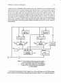
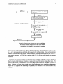
Each RAPIDbus interface card is composed of a series of hnctional blocks. This compartmentalization of
function is intended to improve the readability of a design, simplify debugging, and identify functions that
lend themselves to packaging integration. The interface is composed of a window handler, drivers, latches, an
address translation unit, a multicast address generator, a parity check section, a chip select section, a timing
generator, an interrupt control section, and an interface controller. The Ibus links the Versabus port on the
top of each interface card with the RAPIDbus port at the bottom. It comprises the address translation section,
15
RAPIDbus: Architccture and Realization
the drivers, and the latches. The Versabus port, the RAPIDbus port, the multicast address generators, the
parity section, and the chip select section drive or monitor the Ibus. The modules that compose the
RAPIDbus interface card are illustrated in figure 3-2.
b
I
I
Management
Memory
Unit
r1
A ’ L
I
Interrupti
n
1
-
I
1I
1
Buffer
I
I
4 1
Mu1 t i c a s t
Address
Gene r a t o r
- -1
1‘
1
I
Window
Control
RAPIDBUS PORT
Figure 32 Each RAPIDbus interface card is composed of multiple
modules, centered around the bus.
ItAPIDbus: Architecture and Realization
16
The heart of the time multiplexing of the bus is the window handler. The window handler performs three
functions. First it scans for either the interface home window address or the window address of a master for
which this interface is serving as a slave, as determined by the owner of the Ibus. Through the control register
the interface can be configured so as to recognize only one window address for slave accesses. The proper
phase of the interface host clock is selected by the window handler and supplied to the host so as to maximize
the probability that the host will make a bus request which will reach the drivers just before the master
window on the RAPIDbus appears. Each interface port off the RAPIDbus backplane is given a unique
interface window identification. This unique identification provides the window address of the interface
when acting as a master, creates a unique timeout interval for each interface to reduce deadlock, and for the
case of an interface serving only a slave host, it uniquely maps the interface control page of the slave interface
into ths, RAPIDbus physical address space.
The driver section is used to gate the physical address lines, strobes, parity, write, bus error, retry, data
acknowledge. and address modifier lines onto the RAPIDbus during a window as directed by the control
sequencer. When the control sequencer does not indicate that this interface is to drive a given backplane line
in the currenr window, the lines are to be deasserted. Line drive is to commence as soon as the appropriate
window is recognized and last until the next window is recognized.
The latch section holds data at two levels. The first latches all time-multiplexed RAPIDbus lines at the end
of ever- RAPIDbus cycle. During the following RAPIDbus cycle, these latched lines are examined for a slave
refcrence to *is interface card. If thc Ibus is not being requested or in use, and a slave reference to this
interface is detected. then the contents of the first leve! latch are held by the second level latch. ‘Thelatch also
holds the bus window if the Ibus is already allocated to the virtual bus currently sending the bus window at
the first level latch. Under the direction of the control section, lines can be selectively gated onto the Ibus
according the current Ibus master.
Data transfer cxchanges must always be initiated by a master, and each master interface may optionally
haw a address translation unit positioned between the host processor and the RAPIDbus drivers. The
fiinctjon af the address translation unitis to map A8 - A23 to physical addresses PA8 - PA23. In any interface
that incorporates a address translation process unit, the translation must be capable of being circumvented by
clearing bit three in the control register so as to map the Versabus address directly to the RAPIDbus drivers.
The address and data strobes must be delayed until the physical address is valid and rescinded when the
physical address is no longer valid. The lower seven address lines, A 1 - A7 are supplied directly to the driver
section without translation. Bit zero of the control register switches between primary and secondary memory
maps in interfaces that support memory management. Clearing bit zero accesses the primary memory map,
setting bit zero directs the following references for translation by the secondary memory map in the memory
managerncnt unit.
The multicast address generator is required for all interface cards that must function as a slave during a
multicastdata transfer cycle. The master desiring to multicast must set the multicast request bit in his control
register, asking the processor host’s interface to try for ownership of the multicast capability. Bit twelve of the
interface control register is asserted low by the interface to indicate that the multicast capability has been
secured by this interface. Prior to multicast transfers the multicast address generator registers of all interfaces
that are to be multicasted into must be loaded with the base address and the number of words that are to be
multicasted. For interface cards which support master and slave functional hosts, the master occupying the
Versabus port must be asked to initialize his multicast address generator since the MAG registers for a master
RAPIDbus: Architecaire and Realization
17
interface only appear in that master host’s memory map. For slave-only interface hosts, such as a memory
card. the MAG registers are mapped into the RAPIDbus physical address space. Following write instructions
to the multicast reference address will be multiczst to each multicast activated slave card until a slave’s word
count is exhausted or the master stops writing to the multicast address. Each activated slave depends on its
multicast address generator to supply the memory address and maintain the count or words still to be
transferred. The MAG address counter is not incremented and the word count not decremented if BRETRY
is asserted by any interface being multicast into before the broadcast data acknowledge has gone high.
The parity section generates and checks parity during master and slave data transfer operations. When the
interface is acting as a master, the interface parity section generates the physical address parity. If the
interface is a master doing a write, then the interface generates the appropriate data parity, if the data transfer
is a read, then the incoming data parity is check against that transmitted with the data. If the master is
multicasting, then the data parity is generated and sen! along with the data. If the interface is acting as a slave
handling a memory request or intemipt vectcjr request, then the panty of the address lines is compared with
that generated at the slave board. If the slave request is a read then the parity of the data being read is
generated and sent along with the data. For a slave bcing written into, the parity of the incoming data is
checked with that generated by the slave interface. During a memory reference or interrupt handler
transaction a mismatch in address or data parity causes the slave to send retry back to the master. For a
multicast slave reference the parity of the data is generated by the slave and compared with that generated
and sent along with the data by the multicasting master. If the multicast data parity and the slave generated
parity don’t match, then broadcast retry s asserted, reninning the miilticast cycle.
The chip select section serves to direct references by the interface host to the interface control page or
RAPIDbus resources. After address translation is completed, the physical address is compared to the control
page address. If the master reference is not ta the control page, then the reference is directed to the
RAPIDbiis drivers.. If the reference is decoded for the interface control page, then further decoding identifies
the reference as a multicast. multicast control, interface control register, or memory management unit
reference, selecting the appropriate device or in the case of the multicast, the interface RAPIDbus multicast
server.
The timing generation section controls the timing of the interface state sequencing. This section generates
the multicast and regular address strobes when the respective address lines are ready for the RAPIDbus
drivers, and generates decode enables and DTACK for the interface mapped resources.
The interrupt control section supports interrupt generation and interrupt handler vector requesting. This
section presents to the Versabus port on the kierfxe only those interrupts that the interface host is strapped
to uniquely handle. At one of these levels the interface MMU, if present, is strapped to interrupt. The
interface host is able to generate any one cif the seven levels of RAPIDbus interrupts. The interrupt level
being generated by the host is binary encoded so that the latch section can recognize the level of interrupt
being generated by this interface and latch in the interrupt handler request for a vector which will in turn
identify the reason for the interrupt to the interrupt handler. The interrupt controller also recognizes when
the interface host is acting as an interrupt handler, blocking the interrupt handler request from driving the
RAPIDbus until the interface that would like to act as an interrupt handler is driving the interrupt block line.
After the interrupt block line is being driven by this interface, the acknowledge out for the interrupt daisy
chain is delayed by a clock cycle and then supplied to the interrupt acknowledge daisy chain. If the interrupt
acknowledge input is received by an interface and an interrupt handler bus sequence has not been received at
RAP1 Dbus: Architecture and Realization
18
the level gcneratcd by this interface, then the interrupt acknowledge output is driven low. If the interrupt
acknowledge input is received along the daisy chain and the interrupt handler request has been received, then
the interface host has it Versabus ACKIN driven low. The interrupt control section is also responsible for
monitoring the RAPIDbus reset line and driving the interface and host reset lines low if the RAPIDbus reset
line is asserted.
The control section knits together the other function blocks and controls the logical state of the interface.
The ownership of the Ibus is decided by the control section. The interface host bus error, retry, data
acknowledge, and halt is generated by this section. The RAPIDbus timeout timer and retry limit counter are
supplied by the control section. The control section contains the control register which allows dynamic
configuration of the interface parameters such as the masking address, the address translation path, and the
auxillary memory map. Control signals which gate the drivers onto the RAPIDbus, RAPIDbus signals From
the first to second latch levels, and the output enables that gate the second level latch onto the lbus are
controlled here.
3.3 Reading and Writing on the Bus
Read and write operations are the primary transfer operations for inputting or outputting data for further
processing, storage, or display. Both operations are similar in their use of die KAFIDbus virtual bus structure,
differing primarily in the directional configuration of the data lines linking master and slaLe, and in the
handling of the data transfer request by the slave memory system.
3.3.1 Read Operations
Read operations are initiated by an instruction fetch or memory reference within an instruction that is
executed by a Versabus host processor. The read operation involves the RAPIDbus if the addrcss reccived by
the Versabus controller on the Versabus host card is interpreted by the conu.olle: as being within the
RAPIDbus-addressspace, or the master’s interface control page, or the control page of a RAPIDbus slave. If
the Versabus controller on the host card has not already obtained mastership of the RAPIDbus interface card
lbus, then the Versabus controller generates a bus request level one to the interface card. Some Versabus
processor cards support a block move option in which bit five of the Versarnodule control register is set to
initiate a block transfer, holding ontci mastership of the interface Ibus until bit five is cleared.
After the Versabus port has gained mastership of the Ibus, and the DTACK, bus error, and retry signals
have gone high on the Ibus from previous data transfer operations, then the Versabus port drives the address,
address modifier, address strobe, write, longword, and data strobe lines. As soon as the address strobe is
asserted low the address translation chapter of the RAPIDbus interface card begins translation of the upper
address lines A8 through A23. If bit three of the interface control register is cleared, then the Versabus port
virtual address is mapped directly into the RAPIDbus physical address. If bit three of the interface control
register is set then the address is translated by the memory management unit For information on the
translation function performed by the memory management unit, see the section on address translation.
When the address translation process is completed, the’physical address strobe is asserted. The physical data
strobes are also enabled for assertion by the Versabus port.
RIZIWbus: Architecture and Rcalization
19
The physical address is then mapped by the select unit either onto the interface control page to access
control page registers, or to the RAPIDbus virtual bus assigned to this processor. If the reference is mapped
to the processor’s interface control page then the lower bits of address are decoded to sclcct the interface
control page device. If at least one of the data strobes have not been asserted by this time, the interface waits
until one is asserted. When the first data strobe is asserted by the Versabus port, the write line should still be
high, indicating a read operation. The selected control page device then decodes the remaining address bits to
select the required internal register. When the control page device has accessed the requisite internal register
the contents are gated onto the Ibus data lines as selected by the data strobes and the longword control line.
The data acknowledge signal is returned to the processor by the interface control section. ‘The processor
responds by latching in the requested data and removing the address strobe. The interface then removes the
data acknowledge and releases the data lines. If an interface register had been selected that could not be read
then a bus error returns to the processor is place of the data acknowledge, terminating the transfer cycle. If
the transfer was part of a block move then the Ibus would remain allocated to the Versabus port (unless
requested by a higher priority device, see the chapter on the Ibus). If the Ibus were requested by the read
instruction di,-t.ctly,then it would be released by the Versabus port.
A somewhat more complicated chain of events arises when the select unit maps the address to the
RAPICbus address space. The physical address is sent to the driver section, which gates the data transfer
request onto the master’s virtuzl bus (implemented via bus windows, see the chapter on the Ibus). The slave
which handles the address placed on the virtual bus by the driver section may be occupied when the request
first appears, forcing the read request to sit on the virtual bus through seved window cycles. As soon as the
skive interfke bccomes availablc a link is forged between the Versabus port of the master and the Versabus
port swing as a slave for the duration of a single data transfer operation. If neither of the data strobes have
heen asserted the slave must continue to listen to the virtual bus windows until at least one is asserted. If this
is a read operation then the write line will still be high. The memory location referenced by the address is
tben gatcd onto the data lines of the slave and sent to the slave’s interface driver section. The master’s virtual
bus window is uscd to return the data along with the data acknowledge line asserted by the slave. The master
interface is monitoring the data lines on its virtual bus and catches the window returning the data,,signifiedby
the assertion of data acknowledge. The processor responds by removing the address strobe, causing the slave
to drive data acknowledge high and release itself from the master’s virtual bus. If a parity error is generated
by a mismatch in the address or data lines a retry is generated by the master or slave, terminating the data
transfer cycle. The slave can also assert bus error if an error is present in the request which cannot be resolved
by rerunning the data transfer cycle. Non- answering memory is handled by timing-out and retrying the
mastcr’s request.
3.3.2 Write
Write operations are executed in a manor similar to read operations. They are initiated by a memory
reference within an instruction that is executed by a Versabus host processor. Mapping of the address and
requesting of the Versabus port is analogous to that of a read operation.
On gaining mastership of the Ibus, and noting that DTACK, bus error, and retry have been revoked from
the previous lbus data transfer the Versabus drives the address, address modifier, address strobe, write,
longwgrd, data strobe, and now the data lines. Address translation is accomplished as before with the
exception that a write to a write protected section of memory will result in a bus error to the host processor.
RAPIIIbus: Architecture and Rcalization
20
The select unit maps the physical address either to the interface control page or to the RAPIDbus address
space, and then waits for either of the data strobes to be asserted. Before either of the data strobes are asserted
the write line should have gone low, indicating that a write operation was in progress. If the address
references the interface control page then the required device is selected, followed by the addressed register
internal to the device. An attempt to write into a non-existent or write protected register will result in a bus
error. Assuming the reference is correctly mapped into an interface control page register then the data lines
are gated into the selected register and the interface generates a DTACK back to the Versabus port,
terminating the data transfer operation as before.
If the write operation is mapped to the interface control page multicasting address then a RAPIDous data
transfer to multiple RAPIDbus memory map locations is initiated, supported by the multicasting address
generators on all multicast enabled interface cards. For further details on the multicast mode of data transfer,
see the following section on multicasting.
If the select unit maps the address into the RAPIDbus system address space, either to system memory
locations or the interface control page of a system slave, then the data transfer request is placed on the virtual
bus allocated ta this master via the bus drivers on the master’s interface and the latch section on the intended
slave. The write operation is executed on the virtual bus similar tc the read, except that write is low, causing
the master to drivc the data lines on the virtual bus. The slave returns the d a acknowledge
~
as soon as the
storage operation is completed. Parity errors in the &.ta or address will result in a retry request as before.
During a write operation the slave drives DTACK, retrv, and bus error on the virtual bus.
3.4 Multicast Capability
Multicasting is a special kind of a write data transfer in which there are multiple destination addresses’with
each address on a distinct Versabus host. IJnlike 8 standard write operation in which the address is supplied
by the processor doing the writing, the multicast depends on addresses that are generated on the interface
cards that support each of the host memory locations. These multicast address generators must be setup by
the processor desiring to multicast individually prior to the multicast. Since each interface only has a single
multicast address generator, and there is a single multicast data acknowledge line that is shared by all virtual
buses, the multicast capability must be allocated tc one multicasting processor at a time even though the data
transfer is presented on the multicasting processor’s virtual bus. The high setup overhead of a multicast
operation suggests that the multicast capability should only be used to transfer large blocks of memory to
multiple contiguous memory locations on other cards.
A processor desiring to multicast begins by requesting the system-wide multicast capability. This is
accomplished by setting bit 2 of the processor’s interface control register. The interface then samples the
multicast block line at the beginning of each master home window. If the multicast block line indicates that
the capability is not in use at the beginning of the master’s window, then the interface asserts the line and
becomes the new system multicast master. Bit 12 of the processor’s interface control register is set by the
interface to indicate when the multicast capability is assigned to the requesting interface. The processor may
then begin to setup the multicast base address and word counter on the interface of each of the target
interface cards.
The procedure for initializing the base address and word count on each of the destination interface cards is
21
RAPIDbus: Architecture and Realization
complicated by the configuration of the prospective slave card. Initialization of the multicasting control
registers must be done by a processor operating in the supervisor mode. If a destination memory segmcnt
shares the host card with a processor then the destination interface card's multicast registers are only mapped
into the private address space of the processor that shares the card with the destination memory. The
processor sharing the host card with the destination memory must be interrupted by the processor desiring to
multicast into the card and requested to initialize the multicast address registers as required. The situation is
much simpler in the case of a destination memory card that is slave-only, which is to say thc destination card
does not have a processor on board. These cards map their interface control page onto the RAPlDbus
physical address space, and thus the processor desiring to multicast onto the slave card can initialize the
registers directly.
Address
Word Count
Register
\
7
Mu 1t i p l e x e r
Mu1 t i p l e x e r
Carry
In \
/
AORESS
A 0-7
v
Word
Counter
Carry
out
.+
--
W
Address
Counter
Control
Register
v v
OE
T
ransfer
Complete
DATA
'0-7
-
Data
Mu1 t i p l e x e r
I
Figure 33: Several multicast address generators are needed to
create the hll address range required for a memory
access. A single module is shown here. This illustration
is adapted From Advanced Micro Devices data sheet on
the AMD 2940 [15]
Each multicast address generator, whether mapped onto a private address space or the RAPIDbus address
space is composed of several identical components each as pictured in figure 3-3. In a system that supports a
RAPIDbus: Architecture and Realization
22
24 bit address range, three such blocks are used, driving A1 through A23 (longword, upper data strobe, and
lower data strobe are supplied directly by the multicasting processor during data transfer operations). A 32
bit address range rcquires four address generating blocks. Both address registers and word count registers can
be implemented with either a 24 or 32 bit range. ' R e most significant byte of both registers is thus optional
depending on the option implemented. Writing to the top byte of either address or word count registers
should not produce an error in any implementation that does not support the extended capability. A read of
the top byte in an implementation that does not support the extended range will produce zeros in the top
byte. By writing to the address charged with reinitialization, the last contents which were loaded into a section
can be resupplied to the address countcr and word counter respectively. As long as the word counter is not
zero 3 multicast controller will continue to be "multicast activated". If the physical address region for which
the interface host responds is exceeded before the word count expires, then the multicast data acknowledge
will not be returned by the slave host that exceeded its range, causing a timeout by the multicasting processor,
leading in turn to a retry and eventually a bus error. Any error experienced by a single multicast address
generator must cause all multicast address generators in operation not to increment to the next location or a
decremented word count.
When the multicasting processor has seen to it that all required multicast address registers and word
counters are setup, it is frce to multicast until the highest value word count counter is zeroed or until the
multicas!ing master decides to stop multicasting, whichever is sooner. T h e processor initiates each data
multicast cycle by writing to F7001A and/or F7001B depending on the length of the data to be transferred.
The processor's Versabus port can be requested on a transfer by transfer basis if incoming data is expected
to system memory on the multicasting processor's card during the transfer. A more efficient method of
implementing a multicast operation is to make a block transfcr request through the host controj register,
allocating the multicasting processor's Versabus port to the processor until the port is released. When the
rnulticastirig processor has control over the Versabus port and the interface Ibus, the request proceeds
similarly LO a standard write operation. The memory management unit can be used to translate a processor
supp!ied address into the RAPIDbus multicast address as desired. While in the select section of the
mu1ticasti:ig processor's interface the multicast address is trapped. The data, data strobe, parity, and address
modifier lines are driven onto the processor's virtual bus as before, but the address lines remain high on the
virtual bus. The address strobe is supplemented by a multicast address strobe invoking address generators on
each multicast activated card.
Each slave card is constantly monitoring the multicast address strobe line. Interfaces that are not multicast
enabled drive the multicast data acknowledge line high. Those that are multicast enabled, without an Ibus
owner. and without a pending request for the Ibus latch the virtual bus of the multicasting processor and
initiate a request for the Ibus. As soon as the Ibus is requested and allocated to the multicast data transfer the
data, address modifier, parity, and strobe lines are gated onto the lbus. Unlike a normal write operation the
address is supplied to the multicast address register on each destination interface. The DTACK, bus error,
and retry lines are not driven by each slave back to the processor but rather make use of special open collector
multicast control lines. If multicast retry or multicast bus error is asserted during the transfcr, then all
destination interfaces involved in the multicast freeze their address counters and word counters in preparation
for a retry of the instruction or a bus error handler routine. The multicast activated interfaces drive the
multicast data acknowledge line high as soon as the interface host has completed the data transfer. When all
of the destination interfaces have driven the multicast &ta acknowledge high because they were not multicast
enabled or because they have finished the transfer, then the multicasting processor terminates the data
RAPlDbus: Architecture and Realization
23
transfer. The multicast address strobe is revoked, causing each of the multicast activated interfaces to rescind
the multicast data acknowledge, terminating the data transfer. 'The multicasting processor presents the
multicast address to the processor's interface to initiate another transfer until the highest value word count is
exhausted or the multicasting processor decides to end the multicast process. The multicast capability is then
released by clearing bit 2 of the interface control register.
The multicast capability is a rapid mthod of transferring large data structures to multiple contiguous
address locations on different host cards simultaneously. Since the ability to alter multicast registers requires
a processor operating in the supervisor mode, it is expected that a utility routine will be envoked to multicast,
making many of the initialization details transparent to the applications program.
3.5 Definition of Signal Lines for Data Transfer
The signal lines used by the RAPIDbus protocol EX? based on time multiplexed and extended Versabus
signal lines. RAPIDbus signal lines can be braken up iuto two major groups, those that are time-sliced so that
each processor is the sole owner of them at a given instant in time, and those lines which can be driven and/or
monitored by multiple interfaces simultane~usly. Most of the RAPIDbus lines, paralleling the Versabus
convention. are camed active low.
3.5.1 Time-multiplexed Signal Lines
ACKIN* (Pl: 95) is the input to this interface card from the next lower valued location on the RAPIDbus
backplane interrupt acknowledge daisy chain. This line indicates that the previous card has passed the
interrupt acknowledge daisy chain on, allowing thisherface the option of responding to the interrupt
handler if the interface has generated w1interrupt at the same level that is being serviced by tbe interrupt
handler.
ACKOUT* (Pl: 96) is the output of this interface card going to the next higher valued socket location on
the RAPIDbus backplane. This line is driven low if there is no interrupt handler request pending at the
RAPIDbus port and ACKIN* to this interface from the RAPIDbus is driven low. The line is driven high
when INT.RTN* is asserted on the bus Unlike the Versabus convention, ACKOUT* of the highest
numbered location in the system connects with ACKIN* cif the lowest numbered location to create a circular
interrupt acknowledge daisy chain..
The address modifier lines* (Pl: 59,60,63,83-86,94)provide additional information about the addressing.
The processor function code is inverted and canied in the least three significant bits of the seven address
modifier lines. This function code creates zddress spaces for supervisor program, supervisor data, user
program, and user data. The address modifier lines* are driven during windows in parallel with the address
lines, except during a multicast reference, when the address modifier but not address lines are transmitted
along the virtual bus from master to the slaves. An interface may optionally make latching of a memory
request conditional on a particular function code. For hrther information on address modifier codes, see h e
Versabus specification table 2.1.
The APARITYO* line (p1: 33) is always sent along with the address lines on the bus. It provides even
parity for address bits AOl*-A23*, LWORD*, and AMO*-AM7*.
RAPIllbus: Architecture and Realization
24
'The APARITYl* line (P2: 88) is only driven when the extended address lines option is supported,
providing even parity for A24*- A31*. When the extended addressing option is supportcd, then the
APARITYl* is always sent along with the address lines on the virtual bus.
The As* line (Pl: 30) is used to indicate that a valid address is present in the window for which it is driven.
It is acccptable for a valid address to be driven without As* being driven, but it is not acceptable for As* to be
driven without a valid address, including address modifiers, and address panty bits as supported.
.
The low address lines AOl*-A23* (Pl: 36-58) indicate a specific memory reference which is only to be
decoded by one location in the RAPIDbus physical address space unless the extended addressing option is
supported in which case the extended address bits increase the memory map sizc. The address lines are
driven onto the RAPIDbus only when the interface master owns the Ibus, is not multicasting, and then only
during the interface's home window.
89-96) are supported as an option to further restrict the
The extended address lines A24*-A31* (E:
addressing. They are driven, assuming the option is supported, when the lower address lines are driven.
The bus error signal, BERR* (Pl: 81) indicates that the slave has detected an error during the data
transmission cycle which requires the cycle to be aborted without reuying the data transfer cycle.
The DPARITk'O* - DPARITY3* lines, (Pl: 21,22, P2: 103, lM), represent the even parity f O i the data lines
DOO*-DO?*, D08*-D15*, D16*- D23*, D24*-D31* respectively, and are sent along with each set of data lines
during. 3 transfer. The data parity lines are valid any time the corresponding data lines are valid.
DPARITY2* and DPARI"3* are only driven if the extended data bus option is supported.
The data transfer acknowledge, DTACK* (Pl: 29) is always generated by the slme in a transfer cycle.
During a read cycle the falling edge indicates that the slave is sending valid data during the master's window
which made the request. During a write cycle DTACK* is transmitted back to the mastcr to indicate that the
slave has accepted the data on the bus from the master. DTACK* is rescinded by the slave after AS* goes
high.
The lower data lines, D00*-D15*
(Pl: 5-20), provide a path for data going between master and slave. The
master drives the data lines during its home window if the appropriate data strobe has been asserted and
write* is low, or during a multicast cycle when the master owns the multicast capability. An interface acting
as a slave drives the data lines during the corresponding master's window if write* is high and the appropriate
data strobes have been asserted, or in response to an interrupt handler servicing the level interrupt generated
by the interface host and properly acknowledged along the daisy chain.
The upper data lines, D15*-D31* (P2: 105-120), are optionally supported to create a 32 bit configuration.
These lines are valid only when the appropriate UDS*/LDS* is asserted and LONGWORD* is asserted,
otherwise the window timing of these lines is identical to the lower data lines.
The lower data strobe, L D S (Pl: 25), indicates during byte and word transfers that a data transfer will
occur on DOO*-D07*, and that DPARITYO* will be valid.
RAPIDbus: Architecture and Realization
25
The LONGWORD* signal line (Pl: 35) indicates that a bus cycle is either byte/word (high) or a 32 bit
LONGWORD (low). LONGWOKD is supported only if the 32 bit data path option is implemented.
The multicast address strobe, MAS* (Pl: 64) is driven to indicate a multicast cycle. The MAS* is driven
only when the interface master owns the Ibus, has prepared the proper multicast address generators, and is
driving multiiast.block* line.
The RETRY* line (Pl: 66) is asserted by the slave during the corresponding master’s window to indicate
that the bus cycle must be aborted, with high probability of succeeding if executed again.
The WRITE* line (PI: 34) is asserted by the master on the master’s home window to indicate that the
transfer is a read (high) or a write (low). It is not used to control the drivers until at least one data strobe has
been asserted.
The upper data strobe, UDS* (Pl: 26), indicates during byte and word transfers that a data transfer will
occur on D08*-D15*, and that DPARITYl* will be valid.
3.5.2 Non-Multiplexed Bus Signals
(Note that ECL iiiplementafions will require -5 volts and -2.5 volts bias. This voltage is to be supplied to
:he inierface card through cables leading directly to the appropriate power buses from the interface card.
Optionally iines from the KMIDbus backplane can be assigned to these voltages as long as the allocated lines
on the RAPIDbus are unused by any potential Versabus host. This is to prevent damage in the unlikely event
that a Versabus card is plugged into a RAPIDbus backplane.)
The 4CFAIL line (Pl: 78) is used to indicate that the AC power supply input voltage has fallen below
specified voltage levels, resulting in an imminent failure of the logic power levels.
The ACCLK line (Pl: 69) is optionally supported by the master clock controller card to provide a time base
synchronized to the power line zero voltage crossing points.
The window address lines, ADDR1, ADDRZ, and ADD= (Pl: 19,23,29) designate the master address that
owns the RAPIDbus in order to broadcast a bus window to the first level latch on all interface cards. ADDR3
is the most significant bit of the window address, ADDRl the least. On four master implementations,
ADDR4 is grounded.
The Host Clocks (P2: 79,81,85,87) supply four different equaib spaced phases of the host clock (for the 8
processor system) and two different phases (for the four processor system).
The INT.BLOCK* (Pl: 73) is used to assign the use of the interrupt daisy chain to a particular interrupt
handler. When a master has control over the Ibus, wants to put an interrupt handler request out on the
RAPIDbus, and detects the beginning of the master’s window, then the INT.BLOCK* line is sampled. If it is
high then then the interface desiring to send an interrupt handler cycle drives INT.BLOCK* low and
activates the interface drivers for the remainder of the window, and on all following home windows until the
cycle is completed. On the rising edge of address strobe coming from the interrupt handler master the
RAPlllbus: Architccture and Rcalization
26
IW.BL,OCK signal is released. If the 1NT.BLOCK is sampled and found to be low at the beginning of the
bus cycle then the home window is ignored and the INT.BLOCK line is sampled on the next home window.
The interrupt request lines, IRQl*-IRQ7* (Pl: 87-93), are open collector lines generated by the
interrupter. Level seven is the highest priority. Each master is strapped to act as handler for one or more
interrupt levels. The prioritijration is only invoked if two or more levels are monitored by the same master and
two or more of those lines are pulled at the same time.
The interrupt return line, INT.RTN*, (Pl: 70) is asserted low to indicate that a vector has already been
returned to the interrupt handler who owns the interrupt capability on this interrupt handler cycle. The
interrupt return'line is driven by the interface that is returning an interrupt vector. This line is used to release
all interface cards that have caught the intempt handler bus window as a local reference, but are still waiting
for the interrupt acknowledge down the daisy chain. When two interfaces have generated the same interrupt
level at the Same time, this line allows the second interface down the daisy chain to continue processing while
the first interface supplies a vector to the interrupt handler.
"he MasterCLK line, (Pl: 33) supplies the high speed clock used to control the latches and die interface
state machine. The master clock line is driven by the master clock controller card, originating with the master
oscillator, which also drives the window address counter and the lower speed hosiclocks.
Tbe MLTDTACK line (Pl: 77) is an open collector line which is driven high in respoiise to M A S * bcing
asserted on any window if the interface is not multicast enabled or if the interface has ccmpleted a multicast
write. .
The MLTBERR* line (Pl: 76) is an open collector line which is driven low by either the master or one of
the slaves in response to a multicast data transfer operation that must be aborted. MIdrU3ERR*must be
asserted before BDTACK goes high. MLTBERR is used to abort a cycle that will not succeed if retried.
The MLT.block* line (Pl: 75) is driven low to indicate that a RAPIDbus interface is using the system
multicast capability. An interface, with an Ibus dedicated to the interface master which would like to
multicast, checks the MLT.block line at the beginning of its home window. If the MT,T.blxk line is high at
this time. then the interface desiring to multicast is to drive the MLT.block line low. If the MLT.block line is
low when it is sampled, the interface waits with driving the bus until the next home window, when the line is
sampled again. The line is to be released when the multicast request bit is cleared in the master interface's
control register.
The MLTRETRY* line (Pl: 82) is an open collector line which is driven low in response to a data parity
error detected by a slave that is being multicast into. It is the multicast equivalent of RETRY*. If
MLTRETRY* is generated before the MLTDTACK is removed, then the address generators on all multicast
slaves are not to be incremented.
The two serial reception lines RXDl and RXD2, @2: 61, 55) are reception lines for a terminal or an
external host computer. They follow asynchronous RS-232 convention at the baud rate agreed upon by the
RAPIDbus host and the.terminal or external host computer.
27
RAPIDbus: Architecture and fiealization
The two serial transmission lines TXDl and TXD2, (P2: 63, 57) are transmission lines that complement
RXDl and RXD2. They form the input to the serial ports of the RAPIDbus host computer.
Both the serial reccption ports and the serial transmission ports depend on a clean analog ground for clear,
reliable. and high speed serial transmission. GNDl and GND2, (P2: 65, 59) provide this ground. It is not to
be connected by the KAPIDbus interface, backplane, or to any other grounds. When the connection between
the two elements of the RS232 connection are broken, the serial transmission grounds are to be connected to
the wire that is inputting to the remaining connected system. This avoids noise in the serial transmission
system from affecting either RS232 UART.
The system reset line, SYSRESET* (Pl: 74) is an open collector line which can be pulled by any module in
the system provided the minimum reset interval duration is met. When this line is driven low, all masters,
slaves, and interfaces arc to go into a reset state.
The test configuration lines, TFSTO. & TESTl* (Pl: 65, P1: 79) specify the mode that is to be entered
when the SE’SRESET* line is released.
+
The standby 5 volt power, +5 STDBY (Pl: 133,134) supplies
power IO prevent tlie loss of data.
+5 Vdc to devices requiring continuous
I h e rcgular + S volt power, +5 V (p1: 1, 2,97, 99, 101,103, 105, 129-132, P2: 7-10) supplies the ‘ITL level
logic voltage tcr the interface and processor. Addition power lines may be connected directly to interface or
host.
The +12 volt power (Pl: 125,126,127, 128, P2: 11,12) is supplied primarily to support CMOS and serial
communications lines.
The f 15 volt power (P2: 69,70) is used primarily by analog circuits and is optionally supported.
The -12 volt power (Pl: 121, 122, P2: 15, 16) is supplied primarily to support CMOS and serial
communications lines.
The -15 volt power (P2: 67.68) is used primarily by analog circuits and is optionally supported.
*
RAPIDbus: Architecture and Realization
28
4. The Address System
4.1 Address Translation
The function of the address translation unit on the RAPIDbus interface card is to map the logical addresses
coming from the Versabus host processor into a physical address for use in accessing the host's interface
control page or the RAPIDbus address space. When a logical address is presented to the address translation
section by the Versabus port, one of two routes can be taken to generate the physical address. A direct
mapping of the logical address to the physical address occurs if bit 3 in the interface control register is cleared.
This direct route circumvents the more complex address translation route, decreasing the time required for
the data transfer operation. Setting bit 3 in the intcrface control register routcs the address through a memory
managemcnt unit. Such memory management units mn take much of the burden of memory allocation from
the applications programmer.
Traditionally memory management units have required non-trivial logic complexity .in their
implementation. Recently Motorola has made available a single chip memory management unit allowing
memory protection and relocation capability for a 16 megabyte address space. The Motorola 68451
incorporates greater hnctionality than would be feasible to incorporate on each virtual bus if the memory
management unit were implemented in discrete logic. Thus the RAPIDbus machine level architecture adapts
that of the MC68451. (figure 4-1 illustrates the internal structure of the MC68351)The MC68451 is described
in detail in Motorola publication ADI-872 [16', m d in the MC68000 edition of 16-Bit Microprocessors[17].
It is the intent of this section to summarizc the salient feature of the Me66451 while referring the
programmer to register details in the Motorda c
l
a
y and physical address information in the memory map
section of this report.
4.1.1 Partitioning'of Memory
Several components are used by the memory management unit to establish the full identity of the logical
address that is being supplied to the address translation section. The least three significant bits of the address
modifier lines are inverted to provide the function code generated by the processor when the data transfer was
initiated. This function code identifies the kind of data transfer operation in progress.
The 68000 architecture defines user and supervisor classifications. Within the user and supervisor
classifications, references are hrther subdivided into program and data. A separate function code is used to
designate an interrupt handler cycle which is always routed around the memory management unit by external
logic. These five classes of data transfer operation are further divided into those that are executed in the
primary and those that are executed in the secondary memory map, depending on the state of bit 0 in the
interface control register. Thus the when the host processor is a 68000,ten hnction codes out of sixteen are
assigned to different kinds of data transfer operations within one of two memory map contexts.
The address lines A8 through A23 define a specific location within the logical memory map. The lower
address lines are mapped directly to the physical RAPIDbus, creating a minimum page size of 256 bytes that
can be relocated anywhere in the physical memory map assigned to RAPIDbus that is not otherwise restricted
by the memory management unit or target resource. Through the use of masking bits larger page sizes can be
29
RAPIDbus: Architccture and Realization
LO
Ad
Ai
cal
ess
123
From h o s t
rocessor)
ontrol Register)
b
Cycle
Address
Space
Number
w ite
Pr t e c t
t
ADDRESS
SPACE
TABLE
Address
S ace
Ifask
Address
Space
Number
Write'
dse
Address
Mask
Ph s i c a l
Jase
Address
Lo i c a l
Ad%re s s
I
Logical
Compare
Mask
Mask
Logical
Compare
Compare
Logical
I
P h y s i c a l Rddress
Formation
I
1 o f 32
Descriptors
Address L a t c h
and Compare
Physical
Address
D
T h i s drawing adapted from M o t o r o l a documentation
on t h e MC68451 Memory Management U n i t
To t h e RAPIDbus
Port. Driver Sectlon
Figure 4-1: The MC68451 memory management unit supports
address translation and memory protection.
implemented up to a full 16 megabyte page. The page size is always constrained to be of size 2k where k is an
integer between 8 and 24.
The memory management unit partitions continuous segments in the logical address space. This address
space is shifted by the memory management unit as a block into locations in the physical address space based
on the function code, the logical address, and the preinitialization of the segment descriptor registers.
Segments may be restricted to being user, supervisor, program-only, data-only, or program and data. They
may also be write-protected through the descriptor array. A segment which is accessed with an unacceptable
function code will result in a bus error being taken by the associated processor, terminating the cycle before
the data transfer was delivered to the virtual bus.
RAPID~us:Architecture and Realization
30
A given application task executing on the processor may define one or more segments within the logical
address space as required. Multiple tasks may share the same segment in logical memory. Thus for a general
processor there are 16 logical address spaces, each of 16 megabytes. A number of different tasks can exist
within a single one of these 16 logical address spaces. A unique address space number must be assigned to
each task within a single address space so as to differentiate it from all other tasks in that address space
designated by the hnction code.
4.1.2 Functional Description
During an address translation the inconling function code and memory map line from the interface control
register select one of sixteen, eight bit registers in the address space table. (see figure 4-2 for the address space
table assignments for a 68000 architecture.)The value of this register has been preloaded to indicate the
unique identifying number of tlie task now cxec:i:ing in that hnction code and memory map address space.
This unique identifier is referred to as the cycle address space number in the Motorola literature. For a
correct translation of the address this cycle address space number must match up with the address space
number field in one of the 32 descriptor register mays.
These descriptor arrays consist of nine bytes of information that defines the translation process that is to be
accomplished on the address iines A 8 thro@ A23. These nine bytes must be loaded before use except for
dcscriptor array number one which causes a one to one matching of logical to physical addresses as a default.
(Figure 4-3 depicts the descriptor organizar-ion) Within each of the 32 descriptor arrays there isa 16 bit logical
base address, a logical address mask. a physicd base address, and eight bit locations for the address space
number, segment status register, and the address space mask.
Gnce the cycle address space number has been associatively compared with the address space number in
each of the 32 descriptor arrays the descriptx array for this data transfer cycle should be selected uniquely.
The address space mask allows creating don’t caiie bits in the descriptor address space number entry so that
one descriptor will match with more than one address space number. The selected descriptor logical base
address can be masked by the logical address mask to create segment sizes larger than 256 bytes. When the
mask has been invoked to define the segment size the remaining higher order bits of the logical address which
are not used to map within the segment are replaced by the corresponding physical address bits. Within the
segment the logical address bits are mapped through to the physical address, conceptually similarly to the
mapping that went on with the lowest eight bits of address information.
The physical address thus formed is held by a latch for the remainder of the data transfer cycle. As soon as
the address is valid in thislatch, the physical address strobe is asserted.
4.1.3 Internal Register Manipulation
Before the memory management unit can be used for effective management, a variety of internal registers
which are mapped into the supervisor data space of the processor’s interface control page must be initialized.
The memory management unit resources that are available from the interface control page address space are
summarized in figure 4-4 and figure 4-5
The first sixteen bytes of the memory management unit address space are used to define the unique address
31
JMPI Dbus: Architecture and Realization
Address Space T a b l e O r g a n i z a t i o n
T
0
‘
0
0
P r ima r y
Memory
Map
0
0
0
0
0
1
0
AST 0
1
AST 1
User D a t a 1
0
AST 2
U s e r Program 1
0
AST 3
0
AST 4
0
AST 5
Supervisor Data 1
0
AST 6
S u p e r v i s o r Program 1
0
AST 7
I n t e r p u p t Acknowledge 1
1
AST 8
1
AST 9
1
AST 1 0
i
Secondary
Memory
1
0
1
1
Map
1
1
0
0
1
1
0
1
1
1
1
0
a
I
1
1
-
1
1
I
AST 11
AST 1 2
AST 13
User Data 2
User Program 2
I
Supervisor Data 2
S u p e r v i s o r Program 2
AST 1 5
I n n t e r u p t Acknowledge 2
Figure 4-2: The address space tables links the incoming
function code and memory map bit from the control register
with the cycle address space number [16].
space number assigned to a particular applications task. This value is associatively compared with each of the
values in the 32 descriptor arrays to select the descriptor that is to be used for address translation.
The memory management accumulators are mapped into the next nine bytes of of the memory
management unit address space. The accumulators are used to set each of the 32 descriptor arrays, perform
requested translation of addresses for the use of the supervisor maintenance routines, and to hold information
as the result of a memory management unit fault condition.
32
R A PI Dbu s : Arch i tcciure and Iiealimtion
D e s c r i p t o r s (32)
I
I
Logical Base A d d r e s s
Address Space
I
Number
Segment S t a t u s
ReQ is t e r
System Registers
Address Space
Mask
8 Bits
I
AST15
-4
I
Figure 4-3: The 32 descriptor arrays each define a translation
process. The system registers select the descriptor
array that is to be used during this data transfer cycle
m1.
If the accumulators are to be used for the setting of a descriptor array, then the descriptor pointer is used to
identify the array. The five least significant bits are used to designate the descriptor in load descriptor and
transfer descriptor operations. The reset value of this pointer is 00 hex. During a direct translation operation
for a supervisor maintenance routine, the descriptor pointer is read to determine the segment in which a
match was made. See the Motorola literature or figure 4-6 for further details.
The interrupt vector value is the vector that is returned to the processor during an memory management
unit interrupt sequence to designate the routine that handles memory management unit interrupts.
33
KAPIDbus: Architcciurc and Realization
Memory Management R e g i s t e r Map
HEXAD EC IMAL
ADDRESS
R E G I S T E R OR O P E R A T I O N
K!L
(Address Space Number)
F70067
AC 7
!-us
F70068
AC8
(Address SDace M a r k )
F70066
-
Register)
Figure 4-4: Each processor sees the memory management unit
registers assigned to that unit in the same address locations
WI.
The local and global status registers are each used for interrupt control and fault diagnostics. Both registers
are used by supervisor maintenance routines. A full description of the behavior of both registers can be found
in the Motorola 16-Bit Microprocessor Manual. The registers are summarized in figures 4-7 and 4-8.
RAPJIIbus: Architccturc and Realization
34
Memory Management R e g i s t e r Map
HEXADECIMAL
ADD R E SS
I
R E G I S T E R OR O P E R A T I O N
F70069
DP
Desc r i p t o r P o i n t e r
F7006B
IVR
I n t e r r u p t Vector Register
F7006D
GSR
Global Status
F7006F
LSR
Local S t a t u s
F70071
SSR
Segment S t a t u s and T r a n s f e r
D e s c r i p t o r Ope r a t i o n
F70079
IDP
F7007B
RDP
F7007D
D i r e c t Translation Operation
F7007F
Load D e s c r i p t o r O p e r a t i o n
[Omrwi s e l
N u l l Operation
Interrupt Descriptor Pointer
Result Descriptor Pointer
Figure 4-5: Continuation of the memory management unit address map
1161.
FAch of the 32 descriptor arrays has a segment status register. These registers can either be loaded by
writing into accumulator 7 and then loading the accumulator into the descriptor array or by writing into
E70071, which writes the byte value offered into the segment status register poiiitcd to by tlic descriptor
pointer. The assignments of bits in the SSR and in the segmenL status registers in each of thc descriptor arrays
is described in the Motorola 16-Bit Manual, and summarized in figure 4-9.
The interrupt descriptor pointer is use by the supervisor interrupt handler routines to indicate which of the
32 descriptors caused an interrupt. If multiple memory management unit interrupts are pending then .the
highest priority descriptor index is returned which has its interrupt pending bit set, starting with descriptor
array 0. See the Motorola literature or figure 4-10.
The result descriptor pointer is used to identify descriptors that are involved in a write violation, a load
descriptor failure, or the descriptor that was selected for a direct translation operation. If several descriptor
arrays meet this criterion then the highest priority descriptor index is returned, starting with descriptor array
0. See the.Motorola literature or figure 4-11.
The direct translation operation is invoked by reading F7007D, translating an address for the supervisor.
The address to be translated is loaded into ACO-AC1, and the address space number is loaded into AC6. The
direct translation operation can then be invoked. If the translation can be made the physical address will then
be loaded into AC4-ACS, and 00 hex is returned to the processor on the data bus. An undefined address
resulting from a direct translation operation will return FF hex to the processor.
3s
RAPIDbus: Architecturc 3nd Kealiration
7
6
5
4
3
2
1
0
Desc r i p t o r a r r a y
s e l e c t e d f o r r e a d , load o r
w r i t e segment s t a t u s .
( R e s e t t o 00 Hex)
Reserved
Reserved
Figore 4-6: The descriptor pointer selects the descriptor
array that is used in a load descriptor operation,
read segment status, and the write segment status
operation E161
The lclad descriptor operation is invoked by reading F7007F. Prior to running the load descriptor
operatior. the appropriate accumulator locations must be loaded with the logical base address, the logical
address mask. the address space number., and the address space mask. The operation can now be run. If 00
hex is read from the data bus, then the load was successful. If FF hex was returned then the load was
unsuccesshl. The descriptor that is to be loaded is determined by the descriptor pointer.
All other addrcsses with the memory management section of the control page. as depicted in figure 4-4, are
null operations. All processors that support the memory management unit option map the M M U registers
inta identical addresses as listed in figure 4-4 and 4-5.
4.1.4 System Performance Considerations
Support of the optional memory management unit on one or more of the virtual buses can simplify
RAPIDbus multiprogramming The penalty for this support is paid both in the maintenance overhead needed
to keep the memory management unit registers properly configured and in the increased data transfer access
time for each operation. Routing a data transfer request through the memory management unit instead of the
direct path adds at least 30 nanoseconds to a roughly 500 nanosecond Versabus transfer operation based on an
8 MHz memory management unit.
In order to reduce the burden that is placed on the applications programmer, it is intended that supervisor
36
RAPIDbus: Architectilrc and Realization
I
L
7
6
5
4
3
I
I
L
2
I
1
1
0
I
I
Tr
RESERVED
RE SE RVED
RESERVED
RESERVED
MMU d e t e c t s a f a u l t
while the F f l a g i s set.
MMU d e t e c t s a f a u l t .
Figure 4-7: The Glob& Stams Register summarizes the faults
that haw tmurred and the intcrmpt levels that
are enabled [16]
routines be called, supported by stack parameters to maintain the memory management unit control registers.
Use of a full operating system would increase the transparency and flexibility of the memory management
unit, but at an often heavy decrease in the system thrcuaput. The choice to support memory management
through supervism routines or an operxing system relies heavily on the nature of the applications
environment anticipated. This section documents the use of the interface control register and the location of
RAPIDbus'resources in the 16 megabyte physica! address space of each Versabus host processor when using a
direct mapping between virtual and physical addresses. For hrther information on the use of registers on the
interface host, see the interface host manual.
4.2 Interface Control Register
The Interface control register is used to monitor and alter the configuration of the RAPIDbus interface
card. Interface cards which support a processor host have a corresponding control register which only appears
in the address space of the processor who owns the control register. Interfaces which support a non-processor
host have their control registers mapped into the RAPIDbus address space accessible to all processors. The
interface control register is a full word. The upper byte is read only, whereas the lower byte is readlwrite
enabled.
37
RAPIDbus: Architecturc and Realization
7
6
5
LL'
I
4
I
3
I
2
I
1
I
0
I
i
L
S e t i f a t l e a s t one d e s c r i p t o r has
a pending i n t e r r u p t .
S e t i f ACO, A C 1 , A C 2 , A C 3 , A C 6
and AC8 are globally consistent.
S e t i f A C O , A C 1 , and A C 6
are globally consistent.
R/W*
s t a t u s when f a u l t occurs.
\
Denote s t a t u s o f MMU
after l a s t event.
/
Figure 4-8: The Local Status Register indicates the status of
write* when a fault occurs, the consistency of the descriptors,
and an indication of the highest priority interrupt pending
[I61
4.2.1 Interface Control Register Upper Byte
(See figure 4-12)
(CR 15) Bit 15 of the interface control register is currently unassigned.
RAPIDbus generated the bus error (CR14) When this line is asserted high it indicates that a virtual bus
linked to this interface card.has experienced a bus error since the error trace capability in this control register
was last cleared. (See control register bit 1)
MMU Fault generated the bus error (CR13) This line is only asserted high for an interface card with a
master host and an interface memory management unit. When asserted it indicates that the memory
management unit could not complete the address translation as a result of a write violation or an undefined
segment access since the error trace capability of this control register was last cleared.
Multicast capability assigned(CR12) This line is only asserted high by an interface card which supports a
processor host. It indicates that the host is cleared to Multicast as a result of having asked for the Multicast
capability by setting bit 2 of the interface control register.
Interface address bit 4(CRll) This is the most significant address bit of the interface address. If address bit
38
IbIPIDbus: Architecturc and Realization
Set t o enable t h i s d e s c r i p t o r
i n t h e matching process.
W r i t e p r o t e c t segments
accessed t h r o u g h t h i s d e s c r i p t o r .
S e t i f segment m o d i f i e d
s i n c e i t was d e f i n e d .
I n t e r r u p t pending
.
I n t e r r u p t when d e s c r i p t o r
i s accessed.
Res e r v e d
Reserved
I
S e t i f d e s c r i p t o r accessed
since defined.
Figure 4-9: The segment status register is selected
through the Descriptor Pointer register indirectly [16].
L
L
D e s c r i p t o r c a u s i n g an
i n t e r r u p t as s e l e c t e d
t h e p r i o r i t y encoder.
/
Reserved
Reserved
No i n t e r r u p t p e n d i n g
Figure 4-10: The interrupt descriptor pointer indicates
which descriptor array was in use when an
interrupt was generated [16].
4 is low it indicates that the associated Versabus host has a processor and is capable of initiating data transfer
39
RAPIllbus: Architecture and Realization
7
I
6
I
4-
5
I
4
I
3
I
2
I
1
1
0
I
I
Encode t h e d e s c r i p t o r
a r r a y s e l e c t e d by t h e
p r i o r i t y encoder.
I
/
/
Reserved
S e t if no v a l i d d e s c r i p t o r found.
Figure 4-11: The Kesult Descriptor Pointer identifies the
descriptor involved in a write violation, load
descriptor failurc, or direct translation success
MI.
operations. If bit 4 is high it indicates that the interface host is a slave only card. Only cards with bit four low
have an associated virtual bus and a privaie interface control page.
Interface address bits 1-3 (CR10, CR9, CR8) The lower three interface address lines differentiate between
eight different potential processor cards and eight potential slave-only cards. Each interface must be assigned
a unique combination of interface address lines one through four, and thus a unique window address. For
four processor implementations, CR8 is always zero.
4.2.2 Interface Control Register Lower Byte
(See figure 4-13)
NOTE: On reset all lines in the interface control register lower byte arc cleared to their default state.
Mask out references from all but the mask interface address (CR7) When this line is asserted high it limits
references to the RAPIDbus mapped memory on this interface card to the the processor whose window
address corresponds to the masked address (control register bits four, five, and six).
Mask address 1-3 (CR6, CR5, CR4) The mask address is the window address of the processor card which is
able to make reference to the RAPIDbus mapped memory on this interface card if the interface mask
capability is invoked. The mask capability is invoked by setting bit seven of the control register high.
KAl’IDbus: Architecture and Realization
40
Memory map route enable (CR3) This bit is only meaningful if the interface card has a processor host. The
memory map route enable selects the procedure for mapping from the processor virtual address to the
RAPIDbus physical address. When this bit is low the processor virtual address is mapped directly on the The
RAPIDbus physical address lines. When this bit is set high the mapping operation is accomplished by the
memory management unit, mapping according to the the initialization routines that set up the memory
management unit registers.
Reserve multicast capability (CR2)When this line is asserted high the interface card begins to ask for use of
the multicast capability. When the capability is assigned to this interface card, bit 12 of the interface control
register will be driven high. Then the interface which is assigned the multicast capability can begin to
initialize the required multicast registers on each of the target interface cards holding memory that is to be
reached by the multicast. When the multicast operation is completed the multicasting processor should clear
the reserve multicast capability bit in its interface control register.
Clear bus error record* (CR1) This line is asserted low to clear interface control register bits 13, 14, and 15
and thus the record of what caused a bus error. The bus error handler routine should clear and then set this
bit after reading the interface status to determine the cause of the bus error.
Auxiliary memory map enable (CRO) This line is only used by an interface card with a processor and an
interface memory management unit. It is asserted low to reach the primary memory map in rhe memory
management unit and asserted high to reach the secondary memory map.
1 5 ~ 1 4 ~ 1 3 ~ 1 2 ~ 1 1 )9 11 0 8) 1
2 1
1
0
I
I
I
Mask o u t r e f e r e n c e s f r o m a l l
b u t mask i n t e r f a c e a d d r e s s
Mask a d d r e s s 1
Mask a d d r e s s 2
Mask a d d r e s s 3
Memory map r o u t e e n a b l e
Reserve m u l t i c a s t c a p a b i l i t y
C l e a r bus e r r o r r e c o r d .
A u x i l l a r y memory map e n a b l e
Figure 4-12: Interface control register low byte
1
41
KAPlDbus: Architecture and Rcalization
I
I
7
I
6
4
3
2
1
I
I n t e r f a c e address b i t 1
I n t e r f a c e address b i t 2
I n t e r f a c e address b i t 3
I n t e r f a c e address b i t 4
M u l t i c a s t C a p a b i l i t y Assigned*
MMU F a u l t g e n e r a t e d t h e bus e r r o r
RAPIDbus g e n e r a t e d t h e bus e r r o r
Reserved
Figure 4-13: Interface control register high byte
4.3 EAPlDbus Physical Memory Map
‘The following memory map is based in part on the use of the Motorola VM02 as the host processor. Use of
nL!er hosts may change the location of resources local to the processor. Use of the memory management unit
may cause some or all of the physical addresses to appear in different locations to the processor. Generally
the RAM begins at the low end of the address space with the first and last 2K bytes dedicated to the
supervisor. Up to 256K of EPROM may be supported, extending up into the RAPIDbus address space at
F!00!)@. Dual portcd memory which has a port to both an on board processor and the RAPIDbus memory
space may De configured to map the memory anywhere in the RAPIDbus physical address space beginning
on 256K block boundaries.
42
RAPIDbus: Architecture and Realization
f
f
000100
Unassigned & r e s e r v e d
I
I
Trap i i i s t r u c t i o n v e c t o r s
ooooao
-
---
Unassigned & r e s e r v e d
I
I
I
U n i o t i a l i z e d i n t e r r u p t vector
Unhssigned & r e s e r v e d
I
L i n e 1111 e m u l a t o r
I
1
I
00003D
I
00002D
L i n e 1010 e m u l a t o r
I
000029
Trace
Privilege violation
I
000025
' 000021
Trap V i n s t r u c t i o n
CHK i n s t r u c t i o n
Zero d i v i d e
000014
oooooc
I
I
000008
I
000004
I
000000
000061
I
I
ooooia
000010
000065
Spurious I n t e r r u p t
000060
'
000069
Level 1 i n t e r r u p t autovector
000064
00001c
00006D
Level 2 i n t e r r u p t autovector
oooo6a
000020
000071
Levei 3 i n t e r r u p t autovector
00006C
000024
000075
Level 4 i n t e r r u p t autovector
000070
00002a
000079
Level 5 i n t e r r u p t autovector
000074
00002c
00007D
ILevel 6 i n t e r r u p t a u t o v e c t o r
oooo7a
00003C
ooooai
Level 7 i n t e r r u p t autovector
00007C
000101
Illegal instruction
000011
Address e r r o r
Bus e r r o r
Reset:
Reset:
i n i t i a l program counter
i n i t i a l supervisor stack p o i n t e r
Figure 4-14: Lower RAM supervisorspace
OOOOOD
I
000009
000005
1 oooooi
43
RAPlIIbus: Architecture apd Realijri=ition
f
Brel/AC f a i l vector #
OlFFEE
Group 1 IRQ6 v e c t o r #
OlFFEC
OlFFED
Group 1 IRQ5 v e c t o r #
OlFFEA
OlFFEB
Group 1 IRQ4 v e c t o r #
OlFFE8
OlFFE9
Group 1 IRQ3 v e c t o r #
OlFFE6
OlFFE7
Group 1 IRQ2 v e c t o r #
OlFFE4
OlFFE5
Group 1 IRQl v e c t o r #
OlFFEL
OlFFE3
Unassigned & r e s e r v e d
OlFFEO
OlFFDE
OlFFEF
OlFFEl
Abort vector Y
OlFFDF
,
Group 2 IRQ6 v e c t o r #
01 FFDC
OlFFDD
Group 2 IRQ5 v e c t o r #
OlFFDA
OlFFDB
Group 2 IRQ4 v e c t o r d
OlFFD8
GlFFDS
OlFFD6
OlFFD7
OlFFD4
OlFFD5
Group 2 IRQl v e c t o r #
OlFFD2
OlFFDO
01F800
OlF7FE
OlFFD3
OlFFDl
01F801
OlF7FF
U s e r RAM
000800
.0007FE
0
c)
m
c)
L
n
000400
0003FE
I
000801
0007FF
I
Work a r e a & S u p e r v i s o r S t a c k
000401
0003FF
User i n t e r r u p t vectors
000100
Figure 4-15: User RAM and upper supervisor space
000101
KAPIDbus: Architecture and Realization
I
F70006
F70004
PTM
Read: Read LSB
Buffer register
Write: Write
t i m e r #1 l a t c h e s
I
PTM
Read: Timer
#1 c o u n t e r
W r i t e : Write
MSB b u f f e r r e g i s t e r
PTM
Read: S t a t u s r e g .
Write: Write
C o n t r o l r e g #2
F70002
F70000
F6FFFE
PTY
Read: NOP
W r i t e : (CR20.1)
W r i t e c o n t r o l r e g #1
(CR20-0)
W r i t e c o n t r o l r e q #f
F70007
F70005
F70003
F70001
'GFFFF
Rapidbus Address space
FlOOOl
FlOOOO
FOFFFE
FOFFFF
ROM
FOOOOO
EFFFFE
FOOOOl
EFFFFF
Rapidbus Address space
'200000
!00001
Versabus IRQ7 v e c t o r #
OlFFFE
Versabus IRQ6 v e c t o r #
OlFFFC
Versabus IRQ5 v e c t o r #
OlFFFA
Versabus IRQ4 v e c t o r R
OlFFF8
Versabus IRQ3 v e c t o r I
OlFFF6
Versabus I R Q 2 v e c t o r #
01FFF4
Versabus I R Q l v e c t o r I
OlFFFP
H o s t C o n t r o l r e g i s t e r image
OlFFFO
llFFFF
11FFFD
tlFFFB
11FFF9
11FFF7
IlFFF5
tlFFF3
IlFFFl
T
Figure 4-16: Upper RAM supervisor space, ROM, and Timers
RAPIDbus: Architecture and Realization
45
L
F7002A
F70088
L
Upper M u l t i c a s t Word C o u n t e r
- - - - - - Lower M u l t i c a s t Word C o u n t e r
F70026
l t i c a s t Address R e g i s t e r
- Upper
- M u- - - -
F70024
Lower M u l t i c a s t Address R e g i s t e r
F70022
Upper M u l t i c a s t C o n t r o l R e g i s t e r
F70C20
F7001E
F7001C
F7001A
F70018
F70016
- - - - - - Lower M u l t i c a s t C o n t r o l R e a i s t e r
I l l e g a l address
Interface control register
Master M u l t i c a s t address
Host s t a t u s r e g i s t e r
F70029
F70027
F70025
F70023
F70021
F7001F
F7001D
F7001B
F70019
SERIAL PORTS
Read: P o r t 1 2
S t a t u s Re i s t e r
Write: wr?te p o r t
#2 Command r e g i s t e r
SERIAL PORTS
Read: Read
P o r t 11 s t a t u s r e g .
U
Command
r i t e : Proergt i 11
ster
F70014
F70012
F7002B
F70017
F70015
SERIAL PORTS
Read: P o r t
1 2 Rx d a t a
Write: Write
P o r t 12 Tx d a t a
F70000
SERIAL PORTS
Read: P o r t
#1 Rx d a t a
Urite: Write
P o r t 1 1 Tx d a t a
F7000E
PTM
Read: LSB
Buffer register
Yrite: Yrite
Timer 1 3 l a t c h e s
F70013
F70011
F7000F
DTY
F7000C
F7000D
PTM
Read: LSB
Buffer r e g i s t e r
drite: Write
rimer 12 Latches
F7000A
F7000B
teed: T i m e r
Y2 c o u n t e r
J r i t e : W r i t e MSB
F70008
F70009
7
Figure 4-17: Versamodule registers, and master interface control page
36
KAPIDbus: Architccrilre and Realization
MMU: ASTB (AMMF = I )
F70050
HMU: AST7 ( I n t e r r u p t Acknowledge)
F7004E
MMU: AST6 ( S u p e r v i s o r Program)
F7004C
MMU: ASTS ( S u p e r v i s o r d a t a )
F7004A
MMU: AST4 (AMMF = 0 )
F70048
MMU: ASTB (AMMF = 0 )
F70046
MMU: AST2 ( U s e r p r o g r a m )
F70044
MMU: ASTl ( U s e r d a t a )
F70042
MMU: ASTO (AMMF
F70040
-
0)
F70051
F7004F
F7004D
F7004B
F70049
F70047
F70045
F70043
F70041
F7003E
F7003F
F7003C
F7003D
Reserved M a s t e r .
C o n t r o l Page A d d r e s s i n g
F7003A
F7003B
F70038
F70039
F70036
F70037
Reserved M a s t e r
C o n t r o l Page A d d r e s s i n g
F70034
F70035
F70032
F70033
F70030
F70031
R e i n i t i a l i z e Upper M u l t i c a s t C o u n t e r s
- - - - - -
F7002E
R e i n i t i a l i z e Lower M u l t i c a s t C o u n t e r s
F7002C
v
Figure 4-18: Master interface control page
F7002F
F7002D
47
RAPIDbus: Architecture and Realization
F7041A
F7041B
RAPIDbus A d r e s s Space
F70080
F70081
Load d e s c r i p t o r
F7007E
F7007C
F7007A
F70078
F7007F
I
Direct translation
operation
I
MMU: JDP ( I n t e r r u p t
description pointer
F7007B
F70076
F70074
NULL OPERATION
F70075
F70073
Segment S t a t u s . a n d
Transfer descriptoi
F70070
inn
MMU: LSR ( L o c a l
Status Register)
F7006E
F7006A
F70064
F70062
MMU: AC8 ( A d d r e s s
space m a r k e r )
MMU: AC6 ( A d d r e s s
space number)
F7006D
MMU: I V R ( I n t e r r u p t
Vector r e g i s t e r )
F7006B
MMU: DP ( D e s c r i p t i o
Pointer)
F70069
MMU: AC7
( S t a t u s resister)
F70067
MMU: AC4 ( P B A / T r a n s l a t e d ADDR) AC5
F70065
MMU: AC2 (LAM) AC3
F70063
MMU: ACO ( L B A / T r a n s l a t e ADDR) A C 1
F70060
F70061
MMU: AST15 (AMMF = 1)
F7005E
F7005F
#MU: ASTl4 (AMMF = 1)
F7005C
MMU: ASTl3 (AMMF
F7005A
MMU: AST12 (AMMF
F70058
-
-
F7005D
1)
F7005B
1)
F70059
MMU: A S T l l (AMMF = 1)
F70056
F70057
MMU: ASTlO (AMMF = 1)
F70054
F70071
F7006F
MMU: GSR ( G l o b a l
Status register)
F7006C
F70066
F70079
F70077
F70072
F70068
F7007D
F70055
~~~
MMU: AST9 (AMMF = 1)
F70052
T
.
F70053
Figure 4-19: Master interface control page MMU]
48
RAP1l)bus: Architccturc. and Realization
F7051B
F7051A
R e s e r v e d C o n t r o l Space
F704B1
F704BO
_ _ _ - - - - -
R e i n i t i a l i z e Upper M u l t i c a s t C o u n t e r s
F704AE
F704AF
R e i n i t i a l i z e Lover M u l t i c a s t Counters
F704AD
F704AC
F704AA
F704A8
_ Upper
- -M u l-t i c a-s t Y-o r d -C o u n t e r
F 7 04AB
Lower M u l t i c a s t Word C o u n t e r
F704A9
_ - - - - - -
F704A6
Upper M u l z i c z s t A d d r e s s R e g i s t e r
F704A7
Lower M u l t i c a s t A d d r e s s R e g i s t e r
F704A5
--
F704A4
Upper M u l t i c a s t C o n t r o l R e g i s t e r
F704A2
I
_
_
-
Lover M u l t i c a s t C o n t r o l R e g i s t e r
F704AO
I 1l e g a l a d d r e s s
F7049E
Interface ccntrol register
F7049C
F704A3
-
-
F704A1
F7049F
F7049D
F7049B
F7049A
Reserved C o n t r o l Space
F70431
F70430
_ - - - - - -
R e i n i t i a l i z e Upper M u l t i c a s t C o u n t e r s
F7042E
F7042F
R e i n i t i a l i z e Lower M u l t i c a s t C o u n t e r s
F7042D
F7042C
l t i c a s t Word C o u n t e r
-Upper
-M u- - - -
F7042A
Lower M u l t i c a s t U o r d C o u n t e r
F70428
_ - - - - - -
Upper M u l t i c a s t A d d r e s s R e g i s t e r
F70426
Lower M u l t i c a s t A d d r e s s R e g i s t e r
F70424
lticast Control Register
-Upper
- M u- - - -
F70422
Lower M u l t i c a s t C o n t r o l R e g i s t e r
F70420
I l l e g a l address
F7041E
Interface control register
F7041C
F7042B
F70429
F70427
F70425
F70423
F70421
F7041F
F7041D
7
Figure 4-20: Slave # 1 and Slave # 2 interface control pages
-
-
49
KAPIDbus: Architecture and Realization
F7061A
F7051B
Reserved C o n t r o l Space
F705B3
F705B2
F705BO
F705AE
F705AC
F705AA
R e i n i t i a l i z e Upper M u l t i c a s t C o u n t e r s
- - - - - R e i n i t i a l i z e Lower M u l t i c a s t C o u n t e r s
F705B1
F705AF
l t i c a s t Word C o u n t e r
- Upper
- M u- - - Lower M u l t i c a s t Word C o u n t e r
F705AD
F705AB
F705A8
l t i c a s t Address R e g i s t e r
- Upper
- M u- - - -
F705A9
F705A6
Lower M u l t i c a s t Address R e g i s t e r
F705A7
F705A4
F705A2
F705AO
F7059E
F7059C
_ - - - - - -
Upper M u l t i c a s t C o n t r o l R e g i s t e r
F705A5
Lower M u l t i c a s t C o n t r o l R e g i s t e r
F705A3
I l l e g a l address
F705A1
Interface control register
F7059F
F7059D
Reserved C o n t r o l Space
F70531
F70530
F7052E
F7052C
F7052A
F70528
R e i n i t i a l i z e Upper M u l t i c a s t C o u n t e r s
- - - - - R e i n i t i a l i z e Lower M u l t i c a s t C o u n t e r s
F7052F
F7052D
l t i c a s t Word C o u n t e r
-Upper
- M u- - - Lower M u l t i c a s t Word C o u n t e r
F7052B
F70529
F70526
l t i c a s t Address R e g i s t e r
-Upper
- M u- - - -
F70527
F70524
Lower M u l t i c a s t A d d r e s s R e g i s t e r
F70525
F70522
lticast Control Register
-Upper
-M u- - - -
F70523
F70520
F7051E
F7051C
Lower M u l t i c a s t C o n t r o l R e g i s t e r
F70521
I l l e g a l address
F7051F
Interface control register
.
F7051D
Figure 4-21: Slave #3 and Slave #4 interface control page
50
RAPIDbus: ,Zrchitecture and Realization
F7071A
F7071B
Reserved C o n t r o l Space
F706B3
F706B2
R e i n i t i a l i z e Upper M u l t i c a s t C o u n t e r s
- - - - - -
F706BO
R e i n i t i a l i z e Lower M u l t i c a s t C o u n t e r s
F706AE
l t i c a s t Word C o u n t e r
-Upper
-M u- - - -
F706AC
F706AA
Lower M u l t i c a s t Word C o u n t e r
F706B1
F706AF
F706AD
F706AB
F706A8
l t i c a s t Address R e g i s t e r
-Upper
-M u- - - -
F706A9
F706A6
Lower M u l t i c a s t Address R e g i s t e r
F706A7
F706A4
lticast Control Register
-Upper
-M u- - - -
F706A5
Lower M u l t i c a s t C o n t r o l R e g i s t e r
F706A2
I l l e g a l address
F706AO
Interface control register
F7069E
F7069C
F706A3
F706A1
F7069F
F7069D
Reserved C o n t r o l Space
F70631
F70630
R e i n i t i a l i z e Upper M u l t i c a s t C o u n t e r s
- - - - - -
F7062E
R e i n i t i a l i z e Lower M u l t i c a s t C o u n t e r s
F7062C
l t i c a s t Word C o u n t e r
-Upper
-M u- - - -
F7062A
Lower M u l t i c a s t Word C o u n t e r
F70628
l t i c a s t Address R e g i s t e r
-Upper
-M u - - - -
F70626
Lower M u l t i c a s t Address R e g i s t e r
F70624
lticast Control Register
-Upper
-M u - - - -
F70622
Lower M u l t l c a s t C o n t r o l R e g l s t e r
F70620
I l l e g a l address
F7061E
Interface control register
F7061C
F7062F
F7062D
F7062B
F70629
F70627
F70625
F70623
F70621
F7061F
F7061D
7
Figure 4-22 Slave # 5 and Slave #6 interface control page
51
RAPIDbus: Architecture and liealization
-
F7081A
F7071B
R e s e r v e d C o n t r o l Space
F70783
F70782
R e i n i t i a l i z e Upper M u l t i c a s t C o u n t e r s
- - - - - -
F707BO
R e i n i t i a l i z e Lower M u l t i c a s t C o u n t e r s
F707AE
Y
3
2
B
I=
U
0
1 t i c a s t Word C o u n t e r
- Upper
- M u- - - -
F707AC
F707AA
Lower M u l t i c a s t U o r d C o u n t e r
F70881
F707AF
F707AD
F707AB
F707A8
ess f i e g i s t e r
- Upper
- M u--l t i c a s--t A d d r- -
F707A9
F707A6
Lower M u l t i c a s t A d d r e s s R e g i s t e r
F707A7
F707A4
lticast Control Register
- Upper
- M u-- - - -
F707A5
Y
U
Y
a
Y
#-
c
2
(
cloi
;1
5
v)
Lower M u l t i c a s t C o n t r o l R e g i s t e r
F707A2
I ? l e g a l address
F707AO
-
I n t e r f a c e co!ltrol register
F7079E
F7079C
F70731
R e i n i t i a l i z e Upper M u l t i c a s t C o u n t e r s
- - - - - R e i n i t i a l i z e Lower M u l t i c a s t C o u n t e r s
F7072C
D
2
0
U
F7079F
F7079D
F7072E
P
F707Al
R e s e r v e d C o n t r o l Space
F70730
Y
F707A3
l r i c a s t Word C o u n t e r
-Upper
-M u- - - -
F7072A
F7072F
F7072D
F70726
I-
a!
V
0
Lower M u l t i c a s t Word C o u n t e r
F70728
F70729
U
W
I
=
Y
=
F70726
l t i c a s t Address R e g l s t e r
-Upper
-M u- - - -
F70727
F70724
Lover M u l t i c a s t Address R e g i s t e r
F70725
F70722
lticast Control Register
-Upper
-M u- - - -
F70723
I-
c
(
h
li
Y
>
U
v)
-1
Lower M u l t i c a s t C o n t r o l R e g i s t e r
F70720
F70721
I l l e g a l address
F7071E
U
Interface control register
F7071C
F7071F
F7071D
c
Figure 4-23: Slave # 7 and Slave # 8 interface control page
52
RAPIDbus: Architecture and Realization
FFFFFF
FFFFFE
Rapidbus S h o r t I 1 0
Address Space
FFOOOO
FFOOOl
FEFFFE
FEFFFF
Rapidbus A d d r e s s Space
F82000
F82001
F81FFE
F81FFF
V e r s a b u s I10
Channel
F80000
F80001
F7FFFE
F7FFFF
Rapidbus Address ,Space
F707CO
Figure 4-24: I/O and RAPIDbus address space
F707C1
ILW I )bus: Architccr lire and Ilcalization
53
5. The Priority Interrupt System
5.1 Interrupt System Objectives
functions to divert a sclcctcd proccssor from the normal course of program cxccution
into a service routine that will respond in a timely manor to an event external to the prtmssor’s current
environment. Of particular interest to this document are those interrupts which are generated by one
Vcrsabus host and serviced by a processor on another Vcrsabus host card. Processor hosts whose interface
card supports a memory management unit must respond to MMU intcrrupts as a special CRSC of iritcrrupts
transmitted across the virtual bus. Interrupts that are serviccd by resources on the samc card as the interrupt
was generated on are not specified by eitlier the Versabus specification [3] or by this document.
The
i n ~ c ‘ i-llpt
i
system
‘Ihc Versabus protocol makes use of a daisy chain that assigns a priority to the interrupter that will be
scrviced bascd on physical position in tlic card cage. As a rcsult of the sequential delays inherent in most
implemcntations of a daisy chain structure, it is not practical to time-multiplex this line along N i t h rlic other
common bus lines. Thus all virtual buses in the system must use a common internlpt acknowledge line.
Considcration is quickly given to assigning the unused bus arbitration daisy chains assigned onc tc, each
\irtual bus. ‘I‘his routc has not bcen adapted by chis spccification for two reasons. It is &e intcnt of this
archixcture to specify the RAPIDbus backplane so that if a Vcmbus card is accidently plugged into a
1lAPIDbus backplwc no damage would occur to any clement of the system. Usc of the bus grant lines for
interrupt acknowledge transmission might lead to a improperly placed Versabus card aswniiiig bus
mastership in response to RAPIDbus cards interrupt acknowledge, causing damage to drivcrs on onc or more
cards. A less significant reason is the increased hardware complexity required to suypo:t seven physically
separate interrupt acknowledge lines is probably not worth the increased performance that would result.
Thus it is an objective of the interrupt handler section of each RAPIDbus interface card which supports a
processor to assure that it will be the only master using the interrupt acknowledge daisy chain during a given
interrupt handler cycle, prior to placing an interrupt handler request on its virtual bus.
5.2 Functional Modules
A minimal interrupt system requires an interrupter and an interrupt handler. The proper logic must be
present along the virtual path chosen by the interrupt handlcr so that the interrupter responds correctly with
an interrupt vcctor indicating the response that is requested to the interrupt
The assignment of interrupt handlers to interrupt levels is done at hardware configuration time and in
software. At the Versabus port it is possible for one handler to service all seven interrupt levels. In a system
with seven processors it is possible, and most reasonable, to assign each processor to service one interrupt
levcl. The only restriction on the assignment of interrupt levels to interrupt handlers is that a single handler
must service a contiguous set of interrupt levels, such as levels 3, 4, and 5. It is permissible but probably not
advantageous to have interrupt levels with no handler.
It is the responsibility of the interrupter to identify the interrupt level being handled by the processor that
the interrupter desires to interrupt It is the programmer’s responsibility to see that this information is
available to interrupter software. Some interrupters may be auxiliary resources that are given an assignment
RAPIDbus: Architccturc and Realization
54
by a processor and then set to interrupt the assigning processor when the task is completed. In such a case the
assigning proccssor would prepare a memory location in the interrupting resource that would choose the
interrupt level. In other cases a processor desiring to multicast into memory on the Versabus host of another
processor would ask for the second processor’s multicast address registers to be prepared by interrupting the
second processor.
The interrupt handler considers the interrupts pending which are not masked by the processor or the
processor card at the end of each instruction cycle. The handler asks for a vector indicating the service routine
that is to be performed in an operation similar in many ways to a read operation, as described below. Once
the vector has been read the processor acts to remove the cause of the interrupt and satisfy the demands of the
interrupter.
The RAPIDbus interfaces work to restrict the RAPlDbus system to a single interrupt vector fetch operation
on the system at one time. This is to prevent cocfusion in the assignment of the interrupt acknowledge daisy
chain and the interrupt return vector line. n e RAPIDbus interface assigned to the interrupt handler and all
of the interfaces that physically lie on the interrupt acknowledge daisy chain between handler and interrupter
work to assure that a single interrupter will respond to the interrupt handler at a time. This response causes a
single virtual bus link to be created between interrupt handler and an interrupter active at the same level as
the interrupt handler which is used to obtain the interrupt vector.
5.3 Interrupt Service Protocol
The interrupt service protocol must be initiared by an interrupter. Two cases of an interrupter are handled
separately. If the memory management unit on the RAPIDbus interface of a host processor interrupts the
Versabus port, then’the handlcr request need only propagate down the Ibus with the interrupting MMU and
not onto the RAPIDbus. If the interrupt is generated by the RAPIDbus host and channeled down to the
Versabus port then the inte.rrupt is placed on the RAPIDbus where it is seen by all of the processor hosts in
the system regardless of the virtual bus which they operate on.
The memory management unit will generate an interrupt as a result of an access through a descriptor array
in which the interrupt bit is sef and the interrupt enable bit in the global status register is set. The RAPIDbus
interface must channel this interrupt to the level interrupt that the Versabus host processor is servicing. As
soon as the host processor recognizes this intempt it will request the Ibus. When lbus mastership is granted
to the processor, and the Ibus has been cleared of bus error and the data acknowledge signals from the
previous cycle then the processor will place rhe interrupt handler request on the Ibus in response to the
memory management unit’s request. The lower three address bits will be the value of interrupt which the
memory management unit generated, the address modifier bits will be the interrupt handler code, and write
will be high. Only the lower data strobe is assertcd. The RAPIDbus interface must respond by recognizing
that a memory management unit request is pending at this level and prevent the interrupt handler request
from reaching the virtual bus assigned to this processor. The memory management unit responds by placing
the contents of the interrupt vector register in the MMU on the lower byte of the Ibus data lines. This value-is
read by the processor, multiplied by four, and used to locate the appropriate service routine from the
interrupt handler vector array at the base of local RAM. The Ibus is then released and the chosen handler
routine is initiated. The routine must clear the intempt in the memory management unit prior to enabling
bus interrupts again.
RAP1 Ilbus: Architccture and Rcalization
55
Interrupts by a Versabus host that are channeled to the Versabus port are slightly more complicated to
handle in that the virtual bus link must be complcted between interrupter and the interrupt handler. The
interrupter begins by generating an interrupt on one of the seven interrupt lines at the Versabus port.
Assuming that the interrupter does not activate an interrupt line that it is assigned to service, the request is
placed on the bus.
The interrupt handler that is assigned to service the interrupt level activated notes that the interrupt line
has been asserted when the current instruction is completed and the interrupt handler’s interrupts are
enabled. The handler responds by requesting the Versabus port and Ibus. When mastership has been
granted and the bus error and data acknowledge signals from the previous user of the Ibus have been cleared,
the handler drives the Ibus. The interrupt acknowledge address modifier code is supplied, causing address
translation to be suspended. The lower three bits of the address lines indicate the level interrupt that is being
serviced. The RAPIDbus interface card supporting the interrupt handler samples the IN’I’.BI-OCK line on
the RAPIDbus backplane at the beginning of each home window. If the line is asserted when it is sampled
then the RAPIDbus interface does not drive the home window with the interrupt handler request, but waits
to sample at the next home window. As soon as INT.BLOCK is sampled and found to be high the driver
section gates the interrupt handler request onto the virtual bus assigned to the intsrmpt handler
(implemented during the intempt handler’s hoine window). Simultaneously the interrupt handler interface
asserts INT.BLOCK low for the duration of the interrupt handler data transfer cycle. One latch clock cycle
later the ACKOCTT* line of the interrupt handler interface is driven low.
On each cycle of the interrupt handler’s virtual bus window each interface is examining the address
modfier lines for the interrupt handler code and the address lines for the interrupt level that may have been
generated by the interface host. If a match is found, the interrupter’s Ibus is not in use and no requests are
pending then the intcrrupt handler request is latched at the second level of the interrupt interface’s latch,
along with the interrupt handler’s window address. A request is made for the Ibus of the interrupter. If the
Ibus of the interrupter is in use then the interrupt handler continues to present the interrupt handler request
on its virtual bus until it times-out or the interrupter Ibus becomes available.
The interrupt acknowledge signal propagates down the acknowledge daisy chain from the interrupt
handler. This acknowledge continues around the interrupt acknowledge daisy chain in a locq until it reaches
an interface that has decoded the interrupt handler request at the level at which an interrupt was generated,
and has requested its Ibus. n e interrupt acknowledge daisy chain stops here and is routed to the ACKIN* at
the Versabus port as soon as the Ibus is assigned. Once the interface without a pending interrupt request has
passed the acknowledge on, it must wait for another falling edge of the interrupt acknowledge chain before
considering itself acknowledged. Each interface drives ACKOUT on the RAPIDbus backplane high when
1NT.RTN goes high.
The acknowledged interrupter interface presents an interrupt acknowledge vector request to the Versabus
interface supporting the interrupter. The interrupter responds by providing an interrupt vector directing the
interrupt handler to the routine that will satisfy the interrupter’s need on the lower byte of the data lines.
Data acknowledge is sent back along the virtual bus link to the interrupt handler. The handler reads the
vector and removes its interrupt vector request, releasing the interrupter Ibus and closing the virtual bus link,
The interrupt then vectors to a routine that will remove the cause of the interrupt and provide the required
RAf'IDbus: Architecture and Realization
56
service routine. It is possible that before the interrupt handler gets on the bus to ask for a vector, a second
interrupter will generate an interrupt at the same level that is in the process of being serviced. Thus two
interfaces will latch in the intemipt handler's request but not complete presentation of the interrupt handler
request to the Vcrsabus port. Provision must be made to remove an interrupt handler requests from the Ibus
if the interrupt acknowledge is not received promptly. As soon as an interrupter has been acknowledged it
terminates the acknowledge sequence and drives INT.RTN low to indicate that an interrupt vector is being
returned. This signal causes all other interfaces that have trapped a handler routine to release the request
from their Ibus requester and go about their business until the handler again presents a vector request. The
INT.RTN signal is released by the interrupter at the conclusion of the interrupt handler data transfer.
Thus the priority interrupt system allows any Versabus interrupt card to interrupt any processor which is
set up as an interrupt handler. By responding with a vector detailing the cause of the interrupt, the interrupt
handler can select the appropriate service routine.
RAPIDbus: Architecture and Realization
57
6. lbus Arbitration and Control
6.1 Use of the lbus and Virtual Buses
The Ibus serves as the major data path connecting the Versabus port on the top of each RAPIDbus
interface card with the RAPIDbus port on the bottom of the interface card. The Versabus port sees the Ibus
as the time-static backplane that it is expecting to communicate along, shared by a second potential bus
master, the RAPIDbus port. It is the rcsponsibility of the interface control unit to act as the system controller
for the Ibus according to the Versabus specification, including arbitration of Ibus mastership. In order to
support multiple bus masters on the RAPIDbus simultancously, running on virtual buses, the RAPIDbus
signal lines are time-multiplexed. It is the RAPIDbus port of each interface card which drives. samples, and
latches the time-multiplexed backplanes lines in such a way that the RAPIDbus port looks time-static to the
Ibus. ' h e Versabus port always sees the RAPIDbus port to the Ibus as the local end of the virtual bus that it
believes connects the Versabus port with the rest of the system.
Depending on the resources resident on the interface host card, both the Versabus and RAPIDbus ports
may take on different attributes. Each virtual bus in the system is allocated uniquely to a single Versabus host
processor. If the Versabus port of a given interface card does not have a processor host, then there is no
virtual bus allocated to that interface, and the Versabus port is not enabled to make a request for mastership
of the bus. Versabus hosts that include a processor may request the Ibus at priority level one.
When the processor-equipped Versabus port gains Ibus mastership, the RAPIDbus port of both the master
and the target slave interface card use the virtual bus assigned to the master processor to attempt to complete
the requested data transfer. If the Ibus of the slave interface card is not in use, then the virtual bus assigned to
the master processor will request the Ibus of the slave processor. As soon as this slave Ibus is allocated to the
data transfer from the master processor, a virtual link will extend for the life of a single data transfer operation
from the Versabus port of .the master processor through to the Versabus port of the slave processor. If the
Ibus of the slave processor is already in use then the master processor continues to present the data transfer
request on its virtual bus until the master interface times out or the slave Ibus becomes available.
The virtual link between originator and slave is terminated in one of several ways, each of which is signaled
by the revocation of the address strobe along the virtual link. The read or write protocol may be successhlly
completed along the virtual link by the master and slave Versabus port hosts. Then the returning DTACK
will cause the master processor to'revoke the address strobe, closing the link. Address or data panty may not
match, causing the master Versabus port to receive a signal (implemented via the retry and bus error lines),
which causes the revocation of the address strobe. The slave Versabus host can assert the bus error or retry
lines to terminate the data transfer at its own discretion. If the cycle is terminated using the retry line, then
the master interface card may limit the number ofcycles that are based on the the master host before the retry
is converted to a bus error (which traps to a service routine as opposed to retrying the instruction).
The master RAPIDbus interface card also must provide for virtual links that are never completed, either
because a memory location does not answer, an interrupter does not come back with a vector, or a potential
multicast slave does not release multicast data acknowledge. A sanity timer is started when the address strobe
is asserted. The timing period is set to a unique delay as a function of the window address of the interface
card. When the delay expires a signal is sent to the host processor from its interface if the number of
RAPlDbus: Architccturc and Realization
58
acceptable retries before a bus error has not been reached. Rcuy or bus error will then cause the address
strobe to be revoked.
The RAPIDbus port can act as one of three kinds of Ibus masters depending on the resources on the
interface host card. If Versabus addressable memory is present on the host card, or on the interface control
page then the RAPIDbus port can look like a processor making a memory request (slave reference) to the
Ibus. The RAPIDbus port can also make use of the multicast address generators to multicast into the
Versabus port memory map, causing the RAPIDbus port to look like a multicasting processor. If the Versabus
port is capable of interrupting the RAPIDbus, then the RAPIDbus port can look like an interrupt handler
requesting an interrupt vector (identifying the nature of the interrupt) from the host interrupter. In each of
the these cases, it is not the RAPIDbus port that is actually the originator of the transactioil, but rather the
RAPIDbus port presents a time-static image of the signals that are traveling on a virtual bus connection.
Thus the RAPIDbus port to a given Ibus can act as a slave, working across a virtual bus with a second
RAPIDbus port on another interface card which looks like a master, impiementing what looks like a timestatic Versabus link across time-multiplexed lines. The state behavior of the controller which implements the
required Ibus and RAPIDbus port behavior is shown in state diagrams 6-1 through 6-5
6.2 Master lbus Access
The Versabus host processor can gain access to the off-board RAPIDbus address space via the Jbus for
either a single access or a block move. Executing a read, write, .or read-modify-write to a physical address
which is mapped into the RAPIDbus address space initiates a request to the Ibus for a single data transfer
cycle. Many Versabus host processors also provide a block move option under which bit 5 of the
Versamodule status register is set to one, requesting use of the Ibus and the virtuzl bus assigned to the
processor for one or more data transfer cycles. Under the block move option the processor will be interrupted
when the Ibus and virtual bus are available, possibly at the completion of a mcmory access by another
processor into the memory address space of the processor that has requested a block move. This interrupt
which signals the availability of the Ibus can be masked by clearing bit 8 of the Versakiiodule control register.
After block move mastership has been granted, read, write, or read-modify-writeinstructions can be executed
at an increased rate, needing only to gain access to the Ibus of the slave host to complete the virtual link
between master and slave.
Regardless of how the Versabus host has initiated the request for the Ibus, the request is transmitted from
the master host down to its RAPIDbus interface card by pulling Br #1 low. If the Ibus is not in use and no
requests from the RAPIDbus port are pending, then Bg #1 is issued to the Versabus port by the interface
controller. The interface host processor use of the Ibus is shown in figure 6-1.
After being granted the bus, the host will begin to drive the Ibus lines appropriate to the intended data
transfer operation as soon as the data acknowledge and bus error signals are removed from the preceding data
transfer operation. Address and address modifier lines are always asserted. as soon as the address strobe is
asserted the address translation section of the interface goes to work. If bit 3 of the interface control register is
high, and the function code does not indicate an interrupt handler cycle, then the address and data strobes &e
delayed while the virtual address produced by the Versabus port is translated into the RAPIDbus physical
address. If bit 3 of the interface control register is low, or an interrupt handler cycle is in progress, then the
RAPlDbus: Architccturc and Realization
59
h o s t a d d r e s s space
M u l t i c a s t Reference t o
multicast activated interface
I n t e r r u p t vector request
t o the interface host
\
/
Ibus
Unallocated
To f i g u r e 3
To f i g u r e 4
To f i g u r e 5
Interface host requests
mastership o f the Ibus
>
/
\/
Address
translation
\
/
r
\/
Straight
\ / a d d r e s s mapping
P h y s i c a l address.
P h y s i c a l address.
map ( v i r t u a l a d d r e s s ;
v i r t u a l address
b
J
C
Physical address r e f e r e n c e
t o t h e RAPIDbus a d d r e s s space
c
on t h e RAPIDbus
Gate r e t r y , B e r r . DTACK o n t o
the Ibus.
I f ,UDS o r LDS
i s l o w and w r i t e i s h i g h , g a t e
'data onto t h e Ibus.
No window m a t c h
AS. DTACK.
BERR H i g h
D r i v e A , Am, As. UDS. LDS
LWORD. P a r i t y . & W r i t e on
t h e RAPIDbus b a c k p l a n e .
G a t e r e t r y , B e r r . DTACK o n t o
the Ibus.
I f UDS o r LDS
i s l o w and w r i t e i s l o w t h e n
d r i v e data.
I f UDS o r LDS i s
l o w and w r i t e i s h i g h , g a t e d a t a
onto t h e Ibus
/
Gate r e t r y , B e r r . DTACK o n t o
the Ibus.
I f UDS o r LDS
i s l o w and w r i t e i s h i g h . g a t e
data onto t h e Ibus. Latch t h e
f i r s t l e v e l data i n t o the
second l e v e l l a t c h .
1 Clock c y c l e delay
I
Figure 6-1: A data transfer begins with a master access.
Versabus virtual address is mapped directly into the RAPIDbus physical address. The physical address
validity is signified by the assertion of the physical address strobe.
KAPIDbus: ;2rchitccture and Realization
60
When the physical address strobe has been asserted, then the physical address is compared to the interface
control page address, (F7001A - FSOO7F). If the the translated address docs not refer to the control page, and
the cycle is not an interrupt handler then the physical address strobe and address lincs arc fed to the
RAPIDbus drivers. If the RAPIDbus is selected, then on the next home window the address, address
modifier, address strobe, parity, write, long word, and data strobes are gated onto the RAPIIlbus, and for
each succeeding window until the address strobe and BBSY from the host processor arc revokcd. 'I'he data
lines are bidirectional depending on the state of the write line. Since it is conceivable that on the first window
transmitted to a slave, the request could have a high write line, indicating a read, and on the second the write
fine could be low, indicating a write, no RAPIDbus driver or Ibus gate drives data lines until at least one of
the data strobes has been asserted, indicating that the state of the write line is stable. If at least one of the data
strobes has been asserted and write is high the interface doing the reading gates the data lines, IITACK, ,and
bus error lines from the second level latch onto the Ibus. If at least one of the data strobes has been asserted
by the Vcrsabus host and write is low, indicating a write operation is in progress, then thc interface doing the
writing will drive the data lines on the RAPIDbus on every home window until the data traI:sfcr is completed
or times out. The data acknowledge, retry, and bus error are gated onto the Ibus from t'le second level
RAPIDbus latch. The contents of the second level latch must not be gated onto the lbus until after the first
window has returned from the data transfer slave, once the lines have been tri-stated from the previous data
transfer. An interrupt handler reference is an untranslated reference which does not reach the RAPIDbus
until the master interface has assured that it is the only interface which will be ex'ecuung an interrupt handler
cycle on any of the virtual buses. Once the exclusivity of the interrupt handler is assured &e inrsmpt handler
request proceeds much like a memory reference to the RAPIDbus address space. If the physical address maps
onto the interface control page then further address decoding is done. Figure 6-2 iiiusuatcs the handling of a
control page reference.
It is possible that before an interrupt handler responds to an interrupt request, that interrupt level will be
asserted by more than one interface. An interrupt acknowledge daisy chain is then used to make certain that
only one inremipter at a time supplies an interrupt vector to the interrupt handler. Since this daisy chain line
is shared by each of the virtual buses, only one processor can act as an intempt hacdler at a lime. For further
details of the interrupt protocol, see the chapter on priority interrupts.
References to the control page are sorted into multicast requests, illegal addresses, and references to
registers in the multicast address generator, the memory management unit, and the interface control register.
If the reference is to the multicast request location, then the RAPIDbus drivers are selected as above for a
RAPIDbus address space access with the address strobe replaced with a multicast address strobe. In the case
of a multicast, the address lines are not driven during the home window. Like the interrupt handler request,
the multicast operation is delayed from reaching the RAPIDbus until the master interface has made certain
that it is tlie only virtual bus making a multicast request. This restriction is because the multicast data
acknowledge, multicast bus error, and multicast retry lines are not time-multiplexed, but are shared by all of
the virtual buses. When the master interface is the master of the multicast lines, then the data transfer is
driven onto the RAPIDbus during the home window and is executed similar to a standard memory reference
to the RAPIDbus address space. For hrther details of the multicast protocol, see the multicast protocol
section in the chapter on data transfer operations. An illegal address reference will cause a bus error,
terminating the data transfer cycle. A legal reference ti6 one of the interface registers will cause the interface
to send a DTACK back to the interface host processor, terminating the data transfer cycle.
The Ibus under master ownership is protected from deadlock by a non-answering memory location by the
61
R A PI Dbus: Archi tecr u re and Realization
\
/
From an
unallocated
Ibus
.
\
/
+
Decode t h e i n t e r f a c e page d e v i c e
and s e l e c t .
I
Synchrooous d e l a y
expires
C o n t r o l Page R e f e r e n c e
Read or w r i t e i n t o r e i s t e r s
a s d i r e c t e d by A. w r i f e , and d a t a
strobes.
Synchronous d e l a y
I
G e n e r a t e DTACK t o V e r s a b u s p o r t
1 - 1 Clock c y c l e delay
Return t o
u n a l l o c a t e d bus
I
1
\
Figure 6-2: Control page references are used to modify the
RAPIDbus interface configuration or that of the memory
management unit assigned to the processor's virtual bus.
'Limeout provision on the interface card. Based on the dip header setting, the bus will request a retry at 2,4,8,
16, 32, or 64 microseconds plus a small delay that is based on the interface address. This small skew factor is
intended to prevent reoccurring lockout when two processor cards simultaneously access each other's onboard memory resources. If a DTACK is not received within 2,4,8, or 16 retry cycles, then the retry becomes
a bus mor.
A Versabus hcst processor which has obtained block move ownership of the Ibus is asked to release the
Ibus if a request is made by another virtual bus for access to the Ibus of the interface doing a block move. The
block moving processor is presented with the bus clear signal at Qe Versabus port, asking for the Ibus to be
release. Assigning the lowest priority on the Ibus to the Versabus port favors completing a data transfer
request that is in progress, thus minimizing the possibility of a timeout or a total lockout from a busy
processor.
62
RAPIDbus: Architccturc and Realization
6.3 Memory Access
Mastership of the Ihus belonging to a slave Versabus port by the master RAPIDbus interface is required to
complete a virtual link between two Versabus ports. This mastership is allocated by the slave Ibus controller
for one data transfer at a time. The memory reference access is depicted in figure 6-3.
\
/
unallocated
Ibus
\
Latch t h e f i r s t l e v e l d a t a i n t o
t h e second l e v e l l a t c h .
I
Gate A Am As LDS UDS
LWORC, 'BAS: & W r i t e ' o n t o ' t h e I b u s
I f one o f t h e d a t a s t r o b e s i s
a s s e r t e d and W r i t e i s l o w t h e n
uate data onto the Ibus.
I
match
match
on
I
I
D r i v e DTACK. R e t r y B @ e r r o n t o
t h e Rapidbus b a c k p l a c e . I: o n e
o f the,da:c
strobes i s asserted
and w r i t e i s h7gh. t h e n d r i v e
t h e d a t a l i n e s o n t o t h e RAPIDhus.
Gate A , Am. As, LDS. UDS.
LWORD, BAS. 8 W r i t e o n t o t h e I b u s
*
I
Gate A Am. As. LDS. UDS.
LWORD.'BAS. & W r i t e o n t o t h e I b u s
I f one o f t h e d a t a s t r o b e s i s
a s s e r t e d and W r i t e i s l o w t h e n
a t e data onto the Ibus.
atch the f i r s t l e v e l data i n t o
t h e second l e v e l l a t c h .
Memory Ref e
u
1 Clock c y c l e delay
f
Return t o
u n a l l o c a t e d bus
/
\
Figure 6-3: The memory reference access to the host allows
host processors to examine and modify memory
locations on the host
The first level latch of every RAPIDbus interface card latches in all time-multiplexed RAPIDbus lines on
each window of the bus, cyclically sampling each of the virtual buses. During the window following the
transmission on the bus, the address lines are compared to the address space that is mapped onto each
interface card and the interface host card. If the significant address lines match, the slave Ibus is not in use,
the master interface address is not masked out by the slave interface control register, and no Ibus requests are
1
KAPlDbus: Architecture and Realization
63
in progress, then the output of the first level latch is held by the second level latches. At the same time the
second level latches, the window address of the master processor is held by the window section, and a request
is made for mastership of the slave Ibus by the slave interface KAPIDbus port as a memory reference master
by asserting Ibus Br #2.
When the Ibus of the slave interface is granted to the RAPIDbus port to complete a data transfer, the
appropriate lines are gated onto the slave Ibus. The address, address modifier, As, Write, and data strobe
lines are always asserted. If the Write line is asserted low and either of the data strobes are asserted, then the
data lines are driven onto the slave Ibus, presenting a write request to either the slave Versabus host or the
interface control page if the slave is a slave-only interface which cannot modify its own interface control page.
On subsequent occurrences of the master processor’s window, or virtual bus, the DTACK, I E R R , and retry
lines from the slave Ibus are gated onto the master virtual bus. If the data strobes have been asserted and
Write is high, indicating a read, then the data lines are also driven during the master processor’s window. The
data transfer cycle is completed when the As is removed by the master processor, rdeasing che virtual link
between Versabus ports, freeing the slave Ibus. The master processor must always send at least one window
with address strobe high in order to terminate the link.
Since the virtual bus link between Versabus ports remains open as long as the master processor continues to
assert address strobe, read-modify-write cycles can be handled without iitermpuon. Not asserting
RAPIDbus data line drivers or Ibus gates until at least one data strobe is asserted removes the possibility of
both master and slave processors driving the data lines at the Same time. Problems occur with the 68000
architecture if two processor/slave Versabus hosts each try and access the other’s memory with read-modifywrite instructions. If a deadlock situation results in which neither request can gain mastership over the other’s
Ibus, then at least one will time out, resulting in an attempted retry of a read-modify-write insuuction. Since
the 68000 will not retry a read-modify-write.a bus error will result, trapping to a time consuming bus error.
6.4 Multicast Access
A multicast access request is similar to a memory reference access except that the address is not supplied by
the multicasting master, but rather multicast address generators on each of potentially several (slave)
interfaces. A multicast data transfer cycle also makes use of a special multicast address strobe, and common
open collector multicast data acknowledge lines, multicast retry ,and multicast bus error. The multicast data
transfer operation is summarized in figure 6-4
During the window following that of the multicasting master on the RAPIDbus. the niulticast strobe line
held by the first level latch is examined. Each interface that is multicast activated (has a non-zero word
count), whose Ibus is not in use, with no requests for the Ibus pending. isn’t masking out the multicasting
address, and which receives the multicast address strobe asserted, makes a multicast reference request for the
Ibus. The multicast request causes the window address of the multicaster to be latched in the service window
latch in the window section, and causes the output of the first level RAPIDbus latches to be held at the second
level. If the interface is multicast activated but the potential slave interface Ibus is allocated to another master
or the interface is masking the multicater address thenxhe multicaster continues to leave the data transfer on
the virtual bus until it either times out or all of the multicast activated interface cards respond to the write by
pulling multicast data acknowledge high. The slave interfaces in a multicast data transfer continue to update
the Ibus on each multicaster window until the multicast address strobe is revoked.
64
RAPIDbus: Architccture and Realization
\
1
Ibus
Latch the f i r s t l e v e l data i n t o
t h e second l e v e l l a t c h .
No window match
M u l t i c a s t Ref e rence
G a t e Am, LDS, UDS, d a t a ,
LWORD. BAS. & W r i t e o n t o t h e I b u s
match s e r v i c e
address on
the f i r s t
level latch
h
No window m a t c h
I
G a t e A . Am. A S . LDS. UDS. d a t a .
LWORD. B A S . & W r i t e o n t o t h e I b u s
Latch the f i r s t l e v e l data i n t o
t h e second l e v e l l a t c h .
AS, DTACK,
BERn High
<
Return t o
una1 1o c a t a d bus
1
\
Figure 6-4: The multicast reference to this host allows
multiple locations to be written into simultaneously
If at least one of the slaves in a multicast operation detects a reason to retry the write operation or generate
a bus error, then none of the multicast address generators should increment their counters to keep the DMA
operation in lock step if more than one slave is involved in the multicast write. Retry or bus error requests
must be returned to the multicasting processor using the open collector multicast retry or multicast bus error
lines. Since the normal retry and bus error lines from the slave Veisabus port are not returned to the
multicaster, the multicaster would know nothing about any error they indicate. The millticast or multicast bus
error must be asserted before the last multicast activated interface data acknowledges the multicast cycle.
When the multicast data acknowledge line goes high, then the multicasting Versabus port is fed a DTACK
acknowledge and in turn drives the address strobe high, closing the virtual bus connection.
6.5 Interrupt Vector
If a Versabus host generates a Versabus port interrupt then the interrupt propagates down to non-timemultiplexed RAPIDbus intempt lines that generate an interrupt on the Versabus processor that is strapped to
service the level interrupt generated. Before the interrupted processor can begin the task of servicing the
65
RAPIlIbus: Arcliitecturc and Realization
interrupt, it must obtain a vector from the interrupting processor indicating the reason for the interrupt. This
interrupt handler cycle resembles a master-slave memory reference in many ways. The interrupt handler
cycle is illustrated in figure 6-5.
c
From an
unallocated
Ibus
\
/
\
/
Latch the f i r s t l e v e l data i n t o
t h e second l e v e l l a t c h . Send
i n t e r r u t acknowledge t o t h e
Arsabus port.
O r i v e DTACK. R e t r y & B e r r o n t o
t h e RaDidous b a c k p l a n e .
I f one
o f the d a t a s t r o b e s i s a s s e r t e d
and w r i t e I S h i g h , t h e n d r i v e
t h e d a t a l i n e s o n t o t h e RAPlDbus.
G a t e A . Am. A S , LDS. UDS,
LWORD. SAS. & Wr'te o n t o t h e I b u s
\/
Gate A , Am. As. LDS. UDS.
LWORD. BAS, & W r i t e o n t o t h e I b u s
Ifone o f t h e d a t a s t r o b e s i s
a s s e r t e d and W r i t e i s l o w t h e n
are data onto the Ibus.
atch the f i r s t l e v e l data i n t o
t h e second l e v e l l a t c h .
f
i
Return t o
u n a l l o c a t e d bus
/
\
Figure 6 5 : The intempt handler cycle allows the
interrupting Versabus host to tell the interrupt
handler which service routine to choose to
service the interrupt
The interrupt handler begins by gaining access to its Ibus. After the handler has confirmed that it has
exclusive ownership of the interrupt acknowledge lines, then it drives the interrupt handler request onto the
RAPIDbus during the home window of the interrupt handler. This interrupt handler request is latched in at
the first level of all of the system slaves, then the interrupt acknowledge signal is sent down the non-timemultiplexed interrupt acknowledge daisy chain. The address lines indicate the interrupt level being serviced
by the interrupt handler. If any RAPIDbus interface card detects an interrupt handler request (designated by
RAIWbus: Architcctue and Realization
66
an interrupt handler hnction code), servicing the level interrupt generated by the interface Versabus port,
and the interrupt acknowledge signal is received along the daisy chain, then an interrupt vector request is
made to the interrupter. Ibus. If an interface did not generate an interrupt at the level being handled, then the
interrupt acknowledge signal is passed on down the daisy chain.
This request causes the interrupt handler address to be latched into the service address latch of the window
section, the second level latch holds the output of the first level RAPIDbus latch, and the interrupt handler
request is gated onto the Ibus of the interrupting processor. At the same the interrupt acknowledge signal is
fed to the Versabus port ACKIN. On subsequent occurrences of the interrupt handler window the address,
address modifiers, address strobes, Write, and data strobes are latched at the second level latch of the
interrupting processor. On the same interrupt handler window the data, data acknowledge, retry, and bus
error lines are driven. returning the interrupt vector to the interrupt handler. The virtual bus connection is
closed, freeing the interrupter Ibus when the interrupt handler revokes the address strobe.
6.6 lbus Operation Summary
Thus three major kinds of virtual bus links can be made between two different Versabus ports within the
RAPIDbus system. A memory reference request causes a read or write into memory mapped into the
physical RAPIDbus address space. The multicasting reference allows a write into multiple physical
RAPIDbus locations on different RAPIDbus host cards. ’The interrupt handler vector request specifies the
routine that will satisfy the intempter Each kind of link has its own protocol lines k a t request the slave Ibus
and get the attention of the interface and/or Versabus port resources. Fach interface card functioning as a
systeni slave terminates its virtual bus link with the master when the address strobe is withdrawn, completing
a single data transfer operation. The master in contrast can request use of its Ibus for a block transfer,
maintaining mastership of the lbus until it is requested by another system master trjing to gain access to
resources on the Versabus card of the processor engaged in a block transfer. Ihe Ibus and virtual bus
assigned to each processor are key channels to support multiple processors invohed in simultaneous data
transfer operations.
67
RAPIDbus: Architecrure and Rezlization
7.System Support
7.1 S y s t e m Timing
The bus window mechanism that is used to implement the virtual bus structure is, by nature, synchronous.
Several timing sources based on a single oscillator radiate from the system’s master clock control card. The
master clock is the buffered output of the oscillator. This master clock is used to drive a counter on the master
clock controller card. The lines out of this counter represent the window address lines that are driven on the
backplane, designating the window address of the processor interface that owns the current bus window. The
master clock is also divided down to generate the lower speed clocks that are supplied to the Versabus hosts.
Several different phases of host clocks are generated in order to optimize the initiation of a data request by the
host processor for a particular window address. (See figure 7-1.)
Divider
>>
>
Host
Clocks
I
Master
O s c i 11 a t o r
Buffer
Counter
Master
Clock
>
)
>
>
Window
Addresses
Figure 7-1: All synchronous system timing is derived
from a single time base
7.1.1 The Master Clock
The master clock line on the RAPIDbus backplane is the buffered output of an oscillator on the master
clock controller card. The rising edge of the master clock line on the RAPIDbus is timed to coincide with the
edge transition of the window address, requiring a high slew rate buffer with a delay equal to the delay in the
counter between the clock edge and the changes in the counter output.
The master clock line is used by all of the system interface cards to time the latching of the bus window into
RAPIDbus: Architecture and Rcslization
68
thc first level latch. This line should be seen by all interface cards to go high at the same time in order to
maximize the bus window data transrtiission rate that can be accommodated. The length of the minimal bus
window that can bc reliably run is increased by the maximum possible skew master clock skew as seen by any
two RAPlDbus interface cards. Thus the master clock driver must be chosen for high slew rate, and the
backplane line that supports it should be ideally arranged in a star radiating from the master clock controller
card.
The maximum clock rate that an implementation will support is limited by the maximal frequency at which
bus windows can be run on the RAPIDbus. The minimum acceptable duration of a bus window is a hnction
of the delay in the implementation required to drive the bus, propagate down the backplane, stabilize the bus,
and reliably latch the data driven onto all interface cards at the first level. The time required to activate the
drivers and latch the data includes an often considerable delay while the drivers are coming up to fill current
capability (turn-on) and the hold time during which the data must be stable after it has been "latched". The
propagation time down the backplane arid the required stabilization time are likely to be large factors in the
choice of a a minimum window width.
Two implementations are consideled in companion reports, one in emitter-coupled logic (ECL), and the
other in Advanced Schottky, a TTL subfamily. The implementation technology has a strong effect on the
minimal propagation delay. The technology must either allow thc bus to be critically dampened so that there
is no ringing on the bus after the first edge transition which would be detected as a logical transition, or the
bus must be allowed to settle until the ringing is no ionger significant, and then latched. With ECL it is
practical to drive and receive from the bus witnout diverging from the characteristic impedance of the line
significantly, resulting in a negligible reflection coefficient. TTL drivers have a lower current capability and a
higher output impedance, resulting in ringmg that must be dampened by the bus termination so that the bus
can be latched after an acceptable delay.
Once the minimal bus window length has been chosen there is a question as to how the resulting
bandwidth is to be allocated. Will morz processors be accommodated at a slower host clock speed? Will
fewer processors be allowed to run at a hi_&er host clock frequency? How often will the virtual bus link be
updated; once per host clock cycle, every other cycle, or every fourth host clock cycle? Most high speed
processors exhibit minimal performance degradation when the virtual bus link is updated on every other
clock cycle, permitting the same bus bandwidth to support twice the number of processors. If bus windows
can be reliably handled at 16 MHz (best case for TTL), then four 8 MHz processors can be supported. The
ECL implementation may possibly handled windows at up to 64 MHz, allowing eight advanced 68000
architecture processors to run up to 16 MHz. Such high frequency bus windows in either technology pose a
significant challenge in the implementation.
Thus the chosen clock frequency is highly implementation dependent and is hest determined after a careful
analysis of the implementation bus dynamics. The master clock synchronizes the RAPIDbus interface cards
and is used to derive the host clocks appropriate to the interface address.
69
RAPIIlbus: Architccture and Realization
7.1.2 The Window Address System
The window address system is used to designate the interface which will send a bus window down the
physical RAPIDbus backplane at a particular moment in time. The number of unique addresses is equal to
the maximum number of processor hosts that an implementation can support.
Latch Clock
b
m
P r o c e s s o r 10
P r o c e s s o r 11
Processor 1 2
Processor # 3
Shading i n d i c a t e s t h a t t h e processor
d r i v e s t h e RAPIDbus.
Time
Figure 7-2: An eight processor system requires either
a high bandwidth backplane or a low frequency
processor clock
The anticipated TIL implementation will support four virtual buses corresponding to cycles of four bus
windows before the first virtual bus link is updated again. An additional four slave-only cards are supported
with interface addresses (where the most significant bit of the window address is one), but not assigned virtual
buses. The ECL version is anticipated to support eight virtual buses and thus eight bus windows before the
first virtual bus is again updated. In this larger version the fourth window address bit is one on another eight
slave-only. interface cards which are not assigned virtual buses. The timing of these systems are shown in
figures 7-3 and 7-2 respectively.
The value of the window address lines is incremented such that the updated window address value reaches
the RAPIDbus at the same time that the rising edge.of the clock is reaches the RAPIDbus. In order to
minimize skew in the master clock and window address lines, all must be delivered along equal length runs
from the master clock card to all interface cards.
70
RAPIDbus: ,Irchitccturc and Realization
Latch Clock
P r o c e s c o r U1
k
\
F I
I
h
P
\
1
h
P
\
P r o c e s s o r 13
b
b
\
Processor d 4
I
I
P r o c e s s o r #7
S h a d i n g i n d i c a t e s t h a t t h e processor
d r i v e s t h e RAPIDbus.
J
hb
\
I
I
J
I
Time
Figure 7-3: A four processor system can reasonably be
implemented in Advanced Schottky 'ITL to support
eight MHz processor clocks
Window address lines form the basis for the RAPIDbus realization of a virtual bus structure. The dual
latching level structure effectively separates a complex electro-magnetic transmission problem from the
logical analysis of the bus window which determines the bus window's applicability to a particular interface.
7.1.3 The Host Clocks
The host clocks are the clocks used by each of the interface hosts to regulate their operation. Generally
these clocks operate at a lower frequency than the master clock and the window address lines. Since the host
clock lines are not concerned with the synchronization of spatially distributed elements as the master clock
and window address lines are, transmission along a distributed bus is generally a proper realization technique.
The multiple host clocks differ only in phase and not in frequency. The four processor system supports two
IbWDbus: Architecture and Realization
71
distinct phases, the eight processor system supports four phases. An example of the host processor clocks and
their relation to the other system timing signals is shown in figures 7-2 and figure (timing.1). As a result of the
implementation dependent delays in the interface and the variety of host timings, the correspondence
between window address and clock phase that leads to optimal performance must be determined for a
particular implcrnentation. The pairing shown in figures 3-1 and 7-2 are only intended to be suggestive.
Thus the master clock controller card, situated in the physical center of the RAPIDbus backplane provides
synchronization of the entire system coming from a single clock source. The window addresses and the host
clocks are derived from this master clock in a manner prescribed by the implementation and the host
processor in use.
7.2 Control Lines
The designers of Versabus recognized the need for a variety of utility lines to provide start-up, test
configuration and synchronization to the AC power line. These lines are adapted by the RAPIDbus
specification as lines global to all virtual buses. The ACCLK indicates zero crossings in the AC power.
ACFAIL indicates that the AC power supply voltage has fallen below a preset value and is used to execute an
orderly shut down of the system. System reset is used return the entire RAPIDbus system to an initialized
configuration, either on power up or when directed to do so by the front panel hard reset switch. The two
system test lines. TestO* and Testl* are used to indicate the kind of testing that each Versabus port will
execute on reset
7.2.1 ACCLK
The AC clock is a nominally 60 hz square wave derived from the AC power line. The state of the clock line
is based on thc sign of the AC power line, changing clock state within 95 microseconds of the zero crossing of
the AC power line, The AC clock is generated by the power supply module, and electrically isolated from the
power line,.feeding the RAPIDbus backplane either directly or through the master clock controller card. The
RAPIDbus interface card transmits the AC clock to the Versabus port unaltered for optional use by the
Versabus host. This clock provides a convenient time base for implementation of a time-of-day hnction or
detection of power line frequency zero-point crossings.
7.2.2 Reset
The reset line is an open collector utility line on the RAPIDbus backplane with system-wide meaning. It is
an indication that the system should return to an initialized hardware and software state.
Reset can be asserted in a multitude of ways. The user can initiate a reset via a front panel reset switch, or
optionally via push buttons on any of the Versabus hosts that generate a global (as opposed to local) reset
The power supply can initiate a reset during the power-down sequence as a result of asserting AC failure. At
least two milliseconds after AC failure has been asserted and fifty microseconds before the DC power falls out
of specification, the reset line is to be asserted by the power failure monitor. This prevents random behavior
as a result of uneven power-down sequencing. On power-up the reset line is to be asserted for at least 200
milliseconds after the DC power levels are in specification.
RAP1 Dbus: Architecturc and Realiiation
72
7.2.3 Test Configuration Lines
The test configuration lines indicate the routine that is to be executed at the conclusion of the reset and
initialization sequence following the assertion of reset. Test0 and Test1 are driven by the master clock card
indicating the test configuration. Four modes are available including an immediate monitor entrance mode
(ll), a debug mode (lo), a long test followed by a return to the monitor (Ol), and a less than 2 second test
followed by a vector to the monitor (00). As per the Versabus specification, the master clock control card
must not allow either of the test configuration lines to change state while reset is being asserted.
7.2.4 ACFAIL
The AC failure line is asserted by the power supply system to indicate that the DC power is about to be
removed. It must be asserted at least 4 milliseconds before the DC power falls out G f specification. The line is
routed either directly to the backplane or through the master clock controller card. The RAI’IDbus interface
then routes the AC failure line to the Versabus port without alteration. The master clock card is responsible
for asserting the reset line at least 2 milliseconds after AC failure has been asserted hy the power supply
system and at least 50 microseconds before the DC power falls out of specification.
7.3 I/O Interface
RAPIDbus is intended to be a research too:, supporting application packages that are by nature constantly
in flux, and I/O intensive. Thus the iaterface between the RAPIDbus system and the red world is a critical
facet ofthe system. External interface occurs along four basic paths.
Very high speed input and output, such as bit mapped video, is intended to be handled using special 110
cards such as a frame grabber or video display card. Such cards may take the form of processor/memory
hosts or solely a memory mapped host, depending on the host’s ability to initiate data transfers. Because of
the special nature of such cards, this specification does not attempt to define such special cards except that the
port to the RAPIDbus interface card must subscribe to the Versabus specification.
Lower speed parallel I/O can be accommodated by I/O buses local to a processor or prmessor/memoqy
card, gated from the local processor bus. This specification details a port structure implemented by Motorola
on their VM02 processor/memory cards. This bus provides 4K bytes of memory mapped 110 address space,
four interrupt lines, and a free running 4 MHz clock. Physical mounting of the 110 coiltroller is either
piggy-back to the processor card cr via ribbon cable from the host card to an external control package.
Serial communication with a local network or a terminal is specified to take place over one of two serial
ports on each processor/memory or processor-only host. Port number one is configured to interact with a
terminal. Port number two is configured to port to a local area network as a slave or to a modem. Both ports
are memory mapped and support a variety of baud rates.
The lowest level of system 110 is used to confirm operation of each processor on reset. On reset a test of
the core of each processor is performed, including testing of any on board RAM. When the test is initiated a
red light on the processor card is to be activated. This light is cleared only if the test of each processor core is
successfblly executed. Additional indicator lights may be used on the processor card to facilitate system
1i.APIDbus: Architccrurc and Realization
73
diagnostics. Illc protocol for executing such testing is implementation dependent, and can be found in the
implementation manual for the host under consideration.
7.3.1 I / O B u s
RAPIDbus is targeted for applications which depend on quick, flexible, and reliable communication with
the environment external to RAPIDbus. By using an I/O bus dedicated to each processor, simple 110 can be
accomplished without the considerable complexity and expense of creating a slave I/O card with its own
RAPIDbus port. However restriction to the memory map of only one processor requires a predesignated
processor to handle all 110 interactions with a particular device. Failure of this processor removes the 110
device from the RAPIDbus system. The choice between using a processor I/O bus and a slave interface card
is a decision that must take into account the complexity of the controller, the ability to assign I/O interaction
to a single processor, and the available packaging of OEM controllers.
Two implementations of the local 110 bus architecture are recommended for use on the Versabus
processors used by the RAPIDbus system. The Motorola 110 bus is currently supported by the Motorola
Versrtnioduie computers. It is compact, easily riding piggyback on the processor card or connectcd by up to
twelve feet of ribbon cable to the I10 controller. The STD bus has a similar, although slightly larger form
factox, and a different edge connection scheme. Over seventy companies currently make a range of OEM
boards for the swndard bus in contrast to the single source supply of the Motorola bus. Due to the strong
re!iancc on available OEM nionoboard processor cards, the choice of an I/O bus implementation is largely
determined by the available cards and not the relative merits of the bus.
Following is a description of the Motorola and STD bus architectures. Implementation details are
contained in the Advance Schottky implementation manual for the Motorola 110 bus, which is used in the
cuKent implementation. For further details on the Motorola I10 bus, see Motorola document €30073 [18].
For a description of the SI- bus, see Digital Design, April 1982 [19].
The Motorola I10 bus
The Motorola 110 bus is characterized by a 12 bit address bus, an 8 bit bi-directional data bus,
asynchronous protocol, 4 interrupt lines, an 110 system reset, and a 4 MHz free running clock. The interface
host alwayc acts as a master during data transfer operations with the 110 controller, initiating exchanges. The
I/C bus is mapped into the address space of each processor between F80001 and F81FFF at odd addresses.
The even addresses between F8oooO and F81FFE are illegal.
A strobe and a data acknowledge line are used in the hardware protocol. To execute a write onto the 110
controller the interface host places the address and data on the bus, drives the write line low, and then drives
the strobe line low. The I/O controller responds by recognizing its address, storing the data,and driving the
transfer acknowledge line low. The processor detects the transfer acknowledge line going low, drives the
strobe line high, and continues with the next instruction. The 110 controller detects the revocation of the
strobe line and responds by revoking the acknowledge line.
A read cycle is only slightly more complicated. The interface host places the 110 address on the 110 bus,
drives ;he write line high, and then the strobe line low. The 110 controller recognizes its address, places the
RAPIDbus: Architecturc and Realization
74
requested data on the I/O bus, and drives the acknowledge line low. The interface host receives the
acknowledge, latches in the data, and drives the strobe line high. The 1/0 controller detects the revocation of
the strobc line, stops driving the data bus, and rernoves the acknowledge line.
The Motorola bus is designed so that if a drop cable is used from the monoboard computer, several 110
cards can be chained off the I/O bus. Motorola 110 cards are expected to provide A I D and D/A converters,
as well as a disk controller. The simplicity of the interface leads to the ready design of custom controllers.
The STD Bus
The STD or so called standard bus is a widely supported bus architecture for controller cards with an
increase in flexibility over the Motorola bus. Thc STI) bus is synchronous, with a 56 pin edge connector. It
provides six unidirectional data lines, eight bidir.ectiona1data lines, sixteen address lines, and 22 control lines.
Four power lines provide digital and analog volages. It is widely assumed that a subset of the 56 lines will be
selected for implementation with a particular microprocessor family The STD bus currently supports
peripherals for a large number of microprocessor scnitectures including the 8050, the 8085, the 280, the
6502, the 6800, and the 68000. lEEE has authorized a sroup (p961) to draft an STD bus standard. The very
strong support for this simple, sturdy controlier DUS should merit strong consideration for use in low speed
110 communication.
7.3.2 Serial Access
Multiprocessors have had a reputation among many potential users as being hard to program, difficult to
debug, and nearly impossible to work with in an actual application environment where the multiprocessor
should have been the tool and not the subject. Clearly a good user interface can improve the convenience of
the man-machine interaction. Implementing this user interface within the RAPIDbus system would drain
resources frum the ap.plications package. Thus it is an objective of the RAPIDbus system to condition the
user interface through the use of a front panel promisor. One possible connection arrangement is shown in
figure 1-4.
Communication between RAPIDbus rrnd the front panel processor occurs through two serial lines. The
first line is configured with the RAPIDbus processor acting as "computer" and the front panel processor
acting as "terminal". The second line puts the RAPIDbus processor on the "terminal" end running the
"computer" end through a multiplexer contralled by the front panel processor, connecting finally with a local
area network or external host.
Serial line one coming from each of the RAPIDbus processors must be monitored in preparation for
receiving a message from each of the processors. These messages must be queued by the front panel
processor, identified as to the originating processor, and then presented to the system terminal. Similarly the
user must be able to send commands to a particular processor or subset of processors. It is the responsibility
of the front panel processor to filter the communications so that they are of maximal communicative value to
the user. The front panel processor should be capable of being configured so as to handle some kinds of
requests from RAPIDbus processors internally.
The second serial line comes from each of the RAPIDbus processors, configured as terminals, and must be
75
RAPlDbus: Architecture and Realization
Processor
RAP I D bu s
Processors
Port # 2
(RS 232)
Manual
Ch an ne 1
Select
I
nirprt I i n o s
#
F r o nt
Panel
Processor
RAP ID bus
Processors
Port # 1
(RS 232)
(RS 232 1
System
Terminal
( RS 232)
Figure 7-4: The front panel processor simplifies interactions with
multiple processors.
multiplexed so that one can be connected to a local area network at a time. This multiplexer is under the
control of the front panel processor. If a processor is to'be downloaded, either the RAPIDbus processor to be
downloaded to or the system terminal must make a request for connection between processor and local area
network through the multiplexer. When the use of the serial line is complete, the RAPIDbus processor must
send a message to the front panel processor indicating that the line is available for reallocation.
RAPIDbus: Architecture and Realization
76
The capability of any system element to fail requires the existence of good diagnostic features at all levels of
both hardware and software to maximize the system uptime. Processor cards are specified to be able to
execute functional tests on power-up or reset to verify that the core of each system is functioning correctly.
Similarly the front panel processor must be designed for self testing to verify operation outside of the
RAPIDbus system. The multiplexer must then be capable of connecting a terminal and/or host to each
RAPlDbus processor under user control to execute direct diagnostic control over an independent
processorIRAPIDbus interface system. It is only by being able to break the system in as many independently
verifiable pieces as possible that acceptable mean-time-to-repair will be experienced.
RAPIDbus: Architecture and Realization
77
8 . Where Next?
RAPIDbus is intended as an experiment in multiprocessor interconnect structures. Its secondary hnction
is as a research tool, supporting research in signal processing and system control. The preceding document,
RAPIDbus: Architecture and Realization describes the framework for an experiment. Two following
documents are intended to describe thc i,mplementation of the experiment, and to discuss the results in the
form of both theoretical and run-time performance evaluation. The first of the implementation documents
describes the Advanced Schottky implementahon which is being both constructed and run. The second
implementation document describes a higher performance emitted coupled logic implementation which is
analyzed in terms of theoretical performance. These documents provide the results of the experiment.
Perhaps it is only in these discussions that one has a right to find true conclusions...
78
KAPIDbus: Architecture and Realization
1. Connector CP1 Signals
ODD CONNECTOR PINS
EVEN CONNECTOR PINS
i-5v
1
+ 5v
2
GND
DOO*
DO2*
Do4*
DO6*
DO8*
D10*
D12*
D14*
DPARITYO*
GND
UDS*
GND
DTACK*
GND
APARITYO*
LWORD*
A02*
A04*
A06*
A08 *
A10*
A12*
A14*
A16*
A18*
3
5
7
9
GND
4
6
8
10
12
14
16
18
20
22
A20*
A22*
AM4*
GND
AM3*
TESTO*
GND
ACCLK
GND
INT.BLOCK*
MLT.BLOCK+
MLTDTACK
mTl*
BERR*
AMO*
11
13
15
17
19
21
23
25
27
29
31
33
35
37
39
41
43
45
47
49
51
53
55
57
59
61
63
65
67
69
71
73
75
77
79
81
83
W1*
Do3*
W5*
Do7*
DO9*
D11*
D13*
D15*
DPARITYl*
GND
LDS*
GND
AS*
GND
WRJTE*
A01*
A03*
A05*
A07*
A09*
All*
A13*
A15*
A17*
A19*
A21*
A23*
AM7*
GND
MAS*
RETRY*
GND
INT..RTN
GND
RESET*
MLTBERR*
ACFAIL
NC
MLTRETRY*
AM1*
24
26
28
30
32
34
36
38
40
42
44
46
48
so
52
54
56
58
60
62
64
66
68
70
72
74
76
78
80
82
84
KAPIlIbus: Architecture and Realization
AM2*
IRQ1*
IRQ3*
IRQ5*
IRQ7*
ACKIN*
+5
+5
+5
+5
+5
NC
NC
NC
NC
NC
NC
GND
-12v
GND
12v
12v
5v
5v
5V STBY
GND
GND
GND
+
+
+
+
+
85
87
89
91
93
95
97
99
101
103
105
107
109
111
113
115
117
119
121
123
125
127
129
131
133
135
137
139
79
AM6*
IRQ2*
IRQ4*
IRQ6*
AMs*
ACKOUT*
NC
NC
NC
NC
NC
NC
NC
NC
NC
NC
NC
GND
-12v
GND
12v
12v
5v
5v
5V STBY
GND
GND
GND
+
+
+
+
+
86
88
90
92
94
96
98
100
102
104
106
108
110
112
114
116
118
120
122
124
126
128
130
132
134
136
138
140
80
RAPIDbus: Architccrure and Kcalii-ation
II. Connector CP2 Signals
ODD CONNECTOR PINS
GND
GND
GND
5v
5v
12v
NC
-12v
GND
ADDRl
GND
ADDR2
GND
GND
ADDR3
GND
M AS'I'ERCLK
GND
NC
NC
NC
NC
GND
NC
NC
NC
NC
RXD2
TXD2
GND2
RXDl
TXDl
GNDl
-15
15
GND
NC
NC
NC
Host CK 1
Host CK 2
GND
+
+
+
+
1
3
5
7
9
11
13
15
17
19
21
23
25
27
29
31
33
35
37
39
41
43
45
47
49
51
53
55
57
59
61
63
65
67
69
71
73
75
77
79
81
83
EVEN CONNECTOR PINS
GND
GND
GND
5v
5v
12v
NC
-12v
GND
GND
GND
GND
GND
GND
GND
GND
GND
GND
NC
NC
NC
NC
NC
GND
GND
GND
GND
GND
GND
GND
GND
GND
GND
-15
15
NC
NC
NC
NC
NC
NC
NC .
+
+
+
+
2
4
6
8
10
12
14
16
18
20
22
24
26
28
30
32
34
36
38
40
42
44
46
48
50
52
54
56
58
60
62
64
66
68
70
72
74
76
78
80
82
84
81
RAPIDbus: Architccturc and Kealization
Host CK 3
Host Ck 4
A24*
A26*
A28 *
A20*
GND
NC
GND
DPARITY2*
D16*
D18*
D20*
D22*
D24*
D26*
D28*
D30*
85
87
89
91
93
95
97
99
101
103
105
107
109
111
113
115
117
119
NC
APAKITYl*
A25*
A27*
A29*
A31*
GND
NC
GND
DPARITY3*
D17*
D19*
D21*
D23*
D25*
D27*
D29*
D32*
86
88
90
92
94
96
98
100
102
104
106
108
110
112
114
116
118
120
82
RAPIDbus: Architecture and Realization
Ref e rences
1.
Zwcoli, Mario P. and Sanderson, Arthur C., “Rapid bus Multiprocessor System,” Cornputer Design,
Kovembcr 1981, pp. 189-200.
2.
Bracho, Rafael and Sanderson, Arthur C., “Design of RIP1: An Image Processor for Robotics,” Tech.
report CMU-RI-TR-82-3,Carnegie-Mcllon Robotics Institute, 1982.
3.
Motorola Inc., VersabusSpecificafion Manual, fourth ed., Phoenix, Arizona, 1981.
4.
Dario Giuse Carnegie-Mellon Computer Science Department, DP
1982.
5.
Swan, Richard J., The Switching Sfrucfure and Addressing Archilecture of an Exfensible
Multiprocessor: Cm*, PhD dissertation, Carnegie-Mellon, 1978.
6.
Wulf. William A. and Harbison, Samual A., “Reflections in a Pool of Processors,” Tech.
report CMU-CS-78-103,Carnegie-Mellon Computer Science Department, February 1978.
7.
DEC, VAX Hardware Handbook, Digital Equipment Corporation, Maynard, Mass.,1980.
8.
Langeribach-Belz. M., ”ITT 1230 Exchange: Small Local Version,” Electrical Communicafion, Vol. 54,
bo. 3, September i979, pp. 193-204.
9.
Richards. P.C., ‘TIT 1240 Exchange: Cost Effective Design,” Electrical Communicnfion, Yol. 54, No.
3, September 1979, pp. 205-214.
10.
DEC, PDP- I I Peripherals Handbook, Digital Equipment Corporation, Maynard, Mass.,1973-74.
11.
Halversa Engineering, Synergist Product Specifcation Manual 18597 Paseo Tierra, Saratoga, Ca.,
1982.
12.
Motorola, A468K VMOI Series VersaModule Monoboard Microcomputer User’s Guide. first ed.,
Phoenix, Arizona. 1981.
13.
Motorola, M6PKVMO2 Series VersaModule Monoboard Microcomputer User’s Guide, first ed.,
Phoenix, Arizona, 1982,
14.
Rigger, Chuck, “ZMOB: Doing it in Parallel,” Computer Architecturefor Patfern Analysis and Image
Darubase Managemen4 K. S. Fu, ed., IEEE, Piscataway, New Jersey, November 1981, pp. 119-124.
15.
AMD, Bipolar Microprocessor Logic and Interjace Data Book Advanced Micro Devices, Sunnyvale,
California, 1981.
16.
Motorola, Memory Managemenf Unit (MMU) Advance Information. Phoenix, Arizona, 1981.
17.
Motorola, 16-Bit Microcprocessor User’s Manual Prentice-Hall, Englewood Cliffs, N.J. 07632,1982.
18.
Motorola, IObus SpecifcafionXES0073, first ed., Phoenix, Arizona, 1981.
19.
Snigier, Paul, “The STD Bus,” Digital Design, April 1982, pp. 62-69.
-
Command Sef, Pittsburgh, Pa.,