1
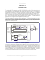
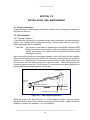
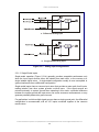
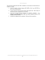
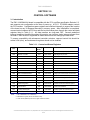
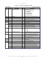
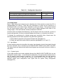
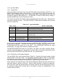
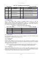
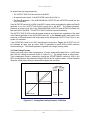
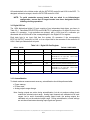
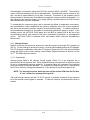
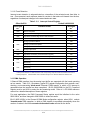
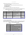
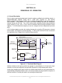
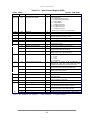
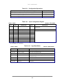
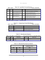
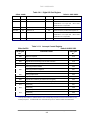
Rev: 090406 PMC-12AISS44AO4 12-Channel, 12-Bit PMC Analog Input/Output Board Eight Simultaneously-Sampled Inputs at 2.0 MSPS per Channel, Four Analog Outputs, and 16-Bit Digital I/O Port _______________________ REFERENCE MANUAL ________________________________________________________________________________________ General Standards Corporation Ph:(256)880-8787 FAX:(256)880-8788 Email: [email protected] MAN-PMC-12AISS44AO4 PMC-12AISS44AO4 Copyright (C) 2004 General Standards Corp. Additional copies of this manual or other General Standards Co. literature may be obtained from: General Standards Corp. 8302A Whitesburg Dr. Huntsville, Alabama 35802 Telephone: (256) 880-8787 FAX: (256) 880-8788 The information in this document is subject to change without notice. General Standards Corp. makes no warranty of any kind with regard to this material, including, but not limited to, the implied warranties of merchantability and fitness for a particular purpose. Although extensive editing and reviews are performed before release to ECO control, General Standards Corp. assumes no responsibility for any errors that may exist in this document. No commitment is made to update or keep current the information contained in this document. General Standards Corp. does not assume any liability arising out of the application or use of any product or circuit described herein, nor is any license conveyed under any patent rights or any rights of others. General Standards Corp. assumes no responsibility resulting from omissions or errors in this manual, or from the use of information contained herein. General Standards Corp. reserves the right to make any changes, without notice, to this product to improve reliability, performance, function, or design. All rights reserved. No part of this document may be copied or reproduced in any form or by any means without prior written consent of General Standards Corp. General Standards Corporation Ph:(256)880-8787 FAX:(256)880-8788 Email: [email protected] PMC-12AISS44AO4 TABLE OF CONTENTS SECTION TITLE PAGE 1.0 INTRODUCTION 1-1 2.0 INSTALLATION AND MAINTENANCE 2-1 2.1 Board Configuration 2-1 2.2 PMC Installation 2-1 2.2.1 Physical Installation 2-1 2.2.2 Input/Output Cable Connections 2-2 2.3 2.3.1 System Configuration Analog Inputs 2-3 2-3 2.3.1.1 Differential Inputs 2-3 2.3.1.2 Single-Ended Inputs 2-4 2.3.2 Analog Outputs 2-5 2.3.2.1 Output Configurations 2-5 2.3.2.2 Loading Considerations 2-5 2.3.3 External Sync I/O 2-6 2.3.4 Multiboard Synchronization 2-7 2.4 Maintenance 2-7 2.5 Reference Verification 2-7 2.5.1 Equipment Required 2-8 2.5.2 Verification and Adjustment 2-8 3.0 CONTROL SOFTWARE 3-1 3.1 Introduction 3-1 3.2 Board Control Register (BCR) 3-2 3.3 Configuration and Initialization 3-2 3.3.1 Board Configuration 3-2 3.3.2 Initialization 3-2 3.4 3.4.1 Analog Inputs 3-4 Input Modes 3-4 3.4.1.1 System Inputs 3-4 3.4.1.2 Test Modes 3-5 General Standards Corporation Ph:(256)880-8787 FAX:(256)880-8788 Email: [email protected] i PMC-12AISS44AO4 `TABLE OF CONTENTS (Continued) SECTION TITLE PAGE 3.4.2 Active Channel Selection 3-5 3.4.3 Input Ranges 3-5 3.4.4 Sampling Modes 3-6 3.4.4.1 Continuous 3-6 3.4.4.2 Burst Sampling 3-6 3.4.5 Input Data Buffer 3-7 3.4.5.1 Organization 3-7 3.4.5.2 Buffer Size and Threshold Registers 3-7 3.5 Analog Outputs 3-8 3.5.1 Output Ranges 3-8 3.5.2 Clocking Modes 3-8 3.5.2.1 Immediate 3-8 3.5.2.2 Simultaneous 3-8 3.6 Data Coding Formats 3-9 3.7 Rate-A/B Generators 3-10 3.8 Multiboard Synchronization 3-10 3.9 Digital I/O Port 3-11 3.10 Autocalibration 3-11 3.11 Interrupt Control 3-12 3.11.1 Organization 3-12 3.11.2 Event Detection 3-13 3.12 DMA Operation 3-13 3.13 Board Configuration Register 3-14 4.0 PRINCIPLES OF OPERATION 4-1 4.1 General Description 4-1 4.2 Analog Inputs 4-2 4.3 Input Data Buffer 4-2 4.4 Analog Outputs 4-2 4.5 Autocalibration 4-2 4.6 Power Control 4-2 App A Local Register Quick Reference A-1 App B Migration from the PMC-12AISS8AO4 B-1 General Standards Corporation Ph:(256)880-8787 FAX:(256)880-8788 Email: [email protected] ii PMC-12AISS44AO4 LIST OF ILLUSTRATIONS FIGURE TITLE PAGE 1.1-1 Functional Organization 1-1 2.2-1 PMC Physical Installation 2-1 2.2-2 System I/O Connector 2-3 2.3-1 Analog Input Configurations 2-4 2.3-2 Output Configurations 2-5 2.3-3 Line Loss Versus Load Current 2-6 2.3-4 Multiboard Synchronization 2-7 2.5-1 Reference Adjustment Access 2-8 3.6-1 Analog Data Coding Formats 3-9 4.1-1 Functional Block Diagram 4-1 LIST OF TABLES TABLE TITLE PAGE 2.2-1 System I/O Connector Pin Functions 2-2 2.5-1 Reference Verification Equipment 2-8 3.1-1 Control and Status Registers 3-1 3.2-1 Board Control Register (BCR) 3-3 3.3-1 Configuration Operations 3-4 3.4-1 Input Configuration Register 3-5 3.4-2 Input Data Buffer 3-7 3.4-3 Input Buffer Threshold Register 3-8 3.5-1 Analog Output Channel Data Register 3-8 3.7-1 Rate Generator Registers 3-10 3.7-2 Rate Generator Frequency Selection 3-10 3.9-1 Digital I/O Port Register 3-11 3.11-1 Interrupt Control Register 3-13 3.12-1 Typical DMA Register Configuration 3-14 3.13-1 Board Configuration Register 3-14 General Standards Corporation Ph:(256)880-8787 FAX:(256)880-8788 Email: [email protected] iii PMC-12AISS44AO4 SECTION 1.0 INTRODUCTION The single-width PCI mezzanine card PMC-12AISS44AO4 provides 12-bit analog input and output capability for PMC applications. Eight analog input channels (Figure 1.1-1) are digitized simultaneously at rates up to 2,000,000 conversions per second per channel, with voltage ranges of ±10V, ±1V or ±100mV. Digitized input data is buffered through a 64 K-sample FIFO. Four 12-bit analog output channels provide software-selected output ranges of ±10V, ±5V or ±2.5V, and are accessed directly through dedicated control registers. A 16-Bit bidirectional digital port can be configured as two independent byte-wide ports. The board is designed for minimum off-line maintenance. All functional parameters are under software control, thereby eliminating field-configuration jumpers. A selftest switching network routes output channels or calibration reference signals to the analog inputs, and permits board integrity to be verified by the host. Loopback Channel-00: One of 8 Identical Input Channels Input Vref 8 Differential Analog Inputs Selftest Switching 12-Bit ADC PGA 12-Bit DAC (4) Input Channels 01-07 Digital I/O (16) and Sync I/O 4 Analog Outputs Local Controller Host Conn (PCI) +5VDC Power Conversion PCI Interface Adapter Regulated Power Voltages Data Buffer Vref Local Bus Figure 1.1-1. Functional Organization This product is functionally compatible with the IEEE PCI local bus specification Revision 2.3, and supports the "plug-n-play" initialization concept. System connections are made at the front panel through a high-density dual-ribbon 80-pin connector. Electrical power is derived from +5VDC supplied by the PCI bus, and analog power voltages are generated internally. Universal signaling is supported, and all operational parameters are software configurable. Operation over the specified temperature range is achieved with conventional convection cooling. ________________________________________________________________________________________ General Standards Corporation Ph:(256)880-8787 FAX:(256)880-8788 Email: [email protected] 1-1 PMC-12AISS44AO4 SECTION 2.0 INSTALLATION AND MAINTENANCE 2.1 Board Configuration This product has no field-alterable configuration features, and is completely configured at the factory for field use. 2.2 PMC Installation 2.2.1 Physical Installation To minimize the opportunity for accidental damage before installation, the board should be stored in the original protective shipping envelope. System power must be turned OFF before proceeding with the installation. CAUTION: This product is susceptible to damage from electrostatic discharge (ESD). Before removing the board from the conductive shipping envelope, ensure that the work surface, the installer and the host board have been properly discharged to ground. After removing the board from the shipping package, position the board with the standoffs facing the host (carrier) board, and with the I/O connector oriented toward the front panel (Figure 2.2-1). Align the two PCI connectors located at the end of the board opposite the I/O connector, with the mating connectors on the host board. Then carefully press the board into position on the host. Verify that the PCI connectors have mated completely and that the standoffs are seated against the host board. PCI Connectors Standoff (2) Host Panel Opening Standoff or PMC Bezel PCI Connectors 2.5mm Mounting Screws (4) Figure 2.2-1: PMC Physical Installation Attach the board to the host with four 2.5 x 6.5mm panhead screws. Pass the screws through the back of the host into the four mounting holes on the board. Tighten the screws carefully to complete the installation. Do not overtighten. ________________________________________________________________________________________ General Standards Corporation Ph:(256)880-8787 FAX:(256)880-8788 Email: [email protected] 2-1 PMC-12AISS44AO4 2.2.2 Input/Output Cable Connections System cable signal pin assignments are listed in Table 2.2-1. The I/O connector is designed to mate with an 80-pin dual-ribbon connector, equivalent to Robinson Nugent #P50E-080-S-TG. The insulation displacement (IDC) Robinson Nugent connector accepts two 40-wire 0.050-inch ribbon cables, with the pin numbering convention shown in Table 2.2-1 and in Figure 2.2-2. Contact the factory if preassembled cables are required. Table 2.2-1. System I/O Connector Pin Functions PIN 1 2 3 4 5 6 7 8 9 10 11 12 13 14 15 16 17 18 19 20 21 22 23 24 25 26 27 28 29 30 31 32 33 34 35 36 37 38 39 40 ROW-A SIGNAL PIN OUTPUT RTN ANA OUT 00 OUTPUT RTN ANA OUT 01 OUTPUT RTN ANA OUT 02 OUTPUT RTN ANA OUT 03 INPUT RTN INPUT RTN INP00 LO * INP00 HI * INPUT RTN INPUT RTN INP01 LO * INP01 HI * INPUT RTN INPUT RTN INP02 LO ** INP02 HI ** INPUT RTN INPUT RTN INP03 LO * INP03 HI * INPUT RTN INPUT RTN INP04 LO * INP04 HI * INPUT RTN INPUT RTN INP05 LO ** INP05 HI ** INPUT RTN INPUT RTN INP06 LO ** INP06 HI ** INPUT RTN INPUT RTN INP07 LO ** INP07 HI ** * Input Group-A. 1 2 3 4 5 6 7 8 9 10 11 12 13 14 15 16 17 18 19 20 21 22 23 24 25 26 27 28 29 30 31 32 33 34 35 36 37 38 39 40 ROW-B SIGNAL DIGITAL RTN DIO 00 DIGITAL RTN DIO 01 DIGITAL RTN DIO 02 DIGITAL RTN DIO 03 DIGITAL RTN DIO 04 DIGITAL RTN DIO 05 DIGITAL RTN DIO 06 DIGITAL RTN DIO 07 DIGITAL RTN DIO 08 DIGITAL RTN DIO 09 DIGITAL RTN DIO 10 DIGITAL RTN DIO 11 DIGITAL RTN DIO 12 DIGITAL RTN DIO 13 DIGITAL RTN DIO 14 DIGITAL RTN DIO 15 VTEST RTN VTEST DIGITAL RTN OUTPUT CLK I/O DIGITAL RTN INPUT TRIG I/O DIGITAL RTN INPUT CLK I/O ** Input Group-B. ________________________________________________________________________________________ General Standards Corporation Ph:(256)880-8787 FAX:(256)880-8788 Email: [email protected] 2-2 PMC-12AISS44AO4 ROW A ROW B PIN 40 I/O CONN PWB PIN 1 Panel Pin-view Figure 2.2-2. System I/O Connector 2.3 System Configuration 2.3.1 Analog Inputs The eight analog input channels can be configured for either differential or single-ended operation. The hardware input configuration must be acknowledged by the control software. 2.3.1.1 Differential Inputs Differential input operation usually provides the best performance, and is essential when the input signal sources are not isolated from each other or have returns that are at significantly different potentials. A potential difference between grounds is significant if it is larger than the maximum tolerable measurement error. This operating mode also offers the highest rejection of the common mode noise that is a characteristic of long cables in typical instrumentation environments. When operating in the differential mode, shown in Figure 2.3-1a, the wire pair from each signal source is connected between the HI(+) and LO(-) inputs of a single input channel. The input return (INPUT RTN in Table 2.2-1) is connected to a ground point that ensures that the sum of the signal level (Vsig) and the common mode voltage (Vcm) remains within the range specified for the board. Ground current through the INPUT RTN line must be limited in order to avoid damage to the cable or the input board. ________________________________________________________________________________________ General Standards Corporation Ph:(256)880-8787 FAX:(256)880-8788 Email: [email protected] 2-3 PMC-12AISS44AO4 a. Differential Analog Input b. Single-ended Analog Input Figure 2.3-1. Analog Input Configurations 2.3.1.2 Single-Ended Inputs Single-ended operation (Figure 2.3-1b) generally provides acceptable performance only when the input signal sources either are isolated from each other, or are common to a single isolated signal return. A single-ended configuration usually is more susceptible to system interference than a differential configuration. Single-ended inputs share a common input return that provides a return path for all inputs, making isolation from other system grounds a critical issue. If the signal sources are returned externally to system ground when operating in this mode, a potential difference between the system ground and input return can cause erroneous measurements, or may generate potentially destructive ground current. For applications in which multiple signal sources share a single ground point, the differential configuration is recommended, with all "LO" inputs connected together at the common remote return. ________________________________________________________________________________________ General Standards Corporation Ph:(256)880-8787 FAX:(256)880-8788 Email: [email protected] 2-4 PMC-12AISS44AO4 2.3.2 Analog Outputs 2.3.2.1 Output Configurations The four analog output channels are single-ended and have a common signal return that is referred to in Table 2.2-1 as OUTPUT RTN. Single-ended outputs should drive only loads that have a high impedance to system ground. The best results are obtained when the loads are isolated also from each other. Figure 2.3-2 shows the primary sources of error in both isolated and nonisolated system configurations. For loads that are isolated from each other (Figure 2.3-2a), the total lineloss error is twice the loss produced in a single line, assuming equal wire size and length for output and return lines. For loads with a common return that is isolated from system ground, line loss in the common return appears as crosstalk between channels. If the load return is connected to a remote system ground (Figure 2.3-2b), the potential difference Vgnd between the remote ground and the internal signal return will introduce an error into the signal delivered to the load. The ground current Ignd developed in the return line is limited essentially only by Rgnd, and can damage the cable or the board if not controlled. OUTPUT BUFFER Vline Vdac Vdac Rline Vline Rline Rload Vload = Vdac - 2Vline Iload a. Isolated Analog Output OUTPUT BUFFER Vline Vdac Iload Rline Vdac Vgnd Ignd Rgnd Rload Vload = Vdac - Vline - Vgnd REMOTE GROUND b. Grounded Analog Output (Not recommended) lcaio12app4 Figure 2.3-2. Output Configurations 2.3.2.2 Loading Considerations The voltage drop in the system I/O cable can be a significant source of error, especially with relatively long cables driving moderate or heavy loads. Figure 2.3-3 shows the effect of load current on the voltage drop in copper wire of various sizes. A 4.0 milliamp load for example, inserts a voltage drop of more than 0.25 millivolt per foot in #28 AWG ribbon cable; twice that if the return line also is considered. Several feet of ribbon cable therefore can produce significant errors, especially in a 12-bit system, in which 1 LSB may represent ________________________________________________________________________________________ General Standards Corporation Ph:(256)880-8787 FAX:(256)880-8788 Email: [email protected] 2-5 PMC-12AISS44AO4 only 1.2 millivolts on a ±2.5 Volt range. High impedance loads generally do not produce significant DC errors. Figure 2.3-3. Line Loss Versus Load Current 2.3.3 External Sync I/O The INPUT CLK I/O, INPUT TRIG I/O and OUTPUT CLK I/O pins in the system connector are bidirectional TTL synchronization signals that provide external control of analog input sampling and analog output clocking. Specific input/output configurations are determined by individual system requirements, and must be acknowledged by the control software. When a board is software-configured as an Initiator, these I/O signals are outputs that can be used to control multiple Target boards. Each clock or trigger event output consists of a 100 nanosecond TTL pulse, asserted LOW. Output loading in the Initiator configuration should be limited to 10 milliamps or less. For Target boards, the I/O signals become inputs and can synchronize input and output operations to an Initiator board. All three inputs are asserted LOW, and are pulled up internally to +5V through approximately 33 KOhms. ________________________________________________________________________________________ General Standards Corporation Ph:(256)880-8787 FAX:(256)880-8788 Email: [email protected] 2-6 PMC-12AISS44AO4 2.3.4 Multiboard Synchronization If multiple boards are to be synchronized together, the INPUT CLK I/O, INPUT TRIG I/O and OUTPUT CLK I/O pins from one board, the initiator, are connected to the corresponding pins of as many as four target boards in the same backplane (Figure 2.3-4). The controlling software determines specific synchronization functions. Target Board #1 (Inputs Control) Input Input Clk I/O Trig I/O (DAC's) Output Clk I/O Target Board #2 Input Input Clk I/O Trig I/O Output Clk I/O Initiator Board Input Clk I/O To Additional Target Boards Input Trig I/O Output Clk I/O (DAC Control) Figure 2.3-4. Multiboard Synchronization 2.4 Maintenance This product requires no scheduled maintenance other than periodic verification and possible adjustment of the internal voltage reference. The optimum verification interval will vary with upon the specific application, but in most instances an interval of one year should be sufficient. In the event of a suspected malfunction, all associated system parameters, such as power voltages, control bus integrity, and system interface signal levels, should be evaluated before troubleshooting of the board itself is attempted. A board that has been determined to be defective should be returned to the factory for detailed problem analysis and repair. 2.5 Reference Verification All analog channels are software-calibrated to a single internal voltage reference by an embedded autocalibration utility. The procedure presented here describes the verification and adjustment of the reference. ________________________________________________________________________________________ General Standards Corporation Ph:(256)880-8787 FAX:(256)880-8788 Email: [email protected] 2-7 PMC-12AISS44AO4 2.5.1 Equipment Required Table 2.5-1 lists the equipment required for verifying or adjusting the internal reference. Alternative equivalent equipment may be used. Table 2.5-1. Reference Verification Equipment EQUIPMENT DESCRIPTION MANUFACTURER MODEL Digital Multimeter, 5-1/2 digit, 0.005% accuracy for DC voltage measurements at ±10 Volts. Input impedance 10 Megohms or greater. Hewlett Packard 34401A Host board with single-width PMC adapter (Existing host) --- Test cable; suitable for connecting the digital multimeter to the system I/O connector. --- --- 2.5.2 Verification and Adjustment The following procedure describes the verification of the internal voltage reference. Adjustment of the internal reference, if necessary, is performed with an internal trimmer that is accessible as shown in Figure 2.5-1. Internal Reference Trimmer Access P2 P1 Shield Figure 2.5-1. Reference Adjustment Access ________________________________________________________________________________________ General Standards Corporation Ph:(256)880-8787 FAX:(256)880-8788 Email: [email protected] 2-8 PMC-12AISS44AO4 This procedure assumes that the PMC is installed on a host board, and that the host is installed in a system. 1. Connect the digital multimeter between ADC VREF (+) Pin-3 and REF RTN (-) Pin-4 in the J2 test connector. 2. If power has been removed from the board, apply power now. Wait at least 10 minutes after power is applied before proceeding. 3. Verify that the digital multimeter indication is +6.000VDC ±0.003VDC. If the indication is not within this range, adjust the internal reference trimmer for an in-range multimeter indication. 4. Verification and adjustment are completed. Remove all test connections. ________________________________________________________________________________________ General Standards Corporation Ph:(256)880-8787 FAX:(256)880-8788 Email: [email protected] 2-9 PMC-12AISS44AO4 SECTION 3.0 CONTROL SOFTWARE 3.1 Introduction The PMC-12AISS44AO4 board is compatible with the PCI Local Bus specification Revision 2.3, and supports auto configuration at the time of power-up. A PLX™ PCI-9080 adapter controls the PCI interface. Configuration-space registers are initialized internally to support the location of the board on any 32-longword boundary in memory space. After initialization is completed, communication between the PCI bus and the local bus takes place through the control and data registers listed in Table 3.1-1. All data transfers are long-word D32. Several predefined interrupt conditions identified throughout this section can invoke a single interrupt request from the board. DMA access is supported for data transfers from the analog input data buffer. To ensure compatibility with subsequent controller revisions, reserved control bits should be written LOW (zero), and maintenance registers should not be modified. Table 3.1-1. Control and Status Registers OFFSET (Hex) REGISTER ACCESS 1 MODE DEFAULT PRIMARY FUNCTION 0000 BOARD CONTROL RW 2302 0000h Board Control Register (BCR) 0004 DIGITAL I/O PORT RW 00XX 00XXh 16-Bit Digital I/O port data 0008 ANALOG OUTPUT CHAN 00 RW 0000 0800h Output Channel 00 data 000C ANALOG OUTPUT CHAN 01 RW 0000 0800h Output Channel 01 data 0010 ANALOG OUTPUT CHAN 02 RW 0000 0800h Output Channel 02 data 0014 ANALOG OUTPUT CHAN 03 RW 0000 0800h Output Channel 03 data 0018 ANALOG INPUT DATA RO 00XX XXXXh Analog input buffer data 001C RATE GENERATOR A RW 0000 0140h Rate-A generator divisor 0020 RATE GENERATOR B RW 0000 3E80h Rate-B generator divisor 0024 INPUT CONFIGURATION RW FF00 0400h Analog inputs channel-mask and burst-size 0028 INPUT BUFFER SIZE RO 0000 0000h Number of data values in the input buffer 002C INPUT BUFFER THRESHOLD RW 0000 FFFEh Input buffer status flag threshold 0030 INTERRUPT CONTROL RW 0000 0000h Interrupt control/status register 0034 Board Configuration RO 00XX XXXXh Firmware revision and hardware options 0038 Autocal Values RW 0000 XXXXh Autocal value readback RW 0000 0000h Auxiliary register. No internal function. --- --- 2 Auxiliary R/W Register 003C 0040-7F Notes: 2 3 (Reserved) Inactive 1. RW = Read/Write, RO = Read-Only. 2. Maintenance register; Shown for reference only. 3. Lower 16 bits (D00-D15) are active; upper 16 bits are all-zero. ________________________________________________________________________________________ General Standards Corporation Ph:(256)880-8787 FAX:(256)880-8788 Email: [email protected] 3-1 PMC-12AISS44AO4 3.2 Board Control Register (BCR) Basic board functions such as initialization, autocalibration and input/output range selection are controlled through the board control register (BCR) shown in Table 3.2-1. Specific control bits are cleared automatically after the associated operations have been completed. Control and monitoring functions of the BCR are described in detail throughout the remainder of this section. 3.3 Configuration and Initialization 3.3.1 Board Configuration During board configuration, initial values for both the PCI configuration registers and the internal control logic are extracted from internal nonvolatile read-only memory. This process is initiated by a PCI bus reset, and should be required only once after the initial application of power. While the PCI configuration registers are being loaded, the response to PCI target accesses is RETRY's. Configuration operations are executed in the sequence shown in Table 3.3-1. Loading of the PCI configuration registers is completed within 3 milliseconds after the assertion of a PCI bus reset. PCI register configuration terminates with the PCI interrupts disabled (Section 3.11). 3.3.2 Initialization Internal control logic can be initialized without invoking a full reconfiguration by setting the INITIALIZE control bit HIGH in the BCR. This action initializes the internal logic, but does not affect the PCI configuration registers and does not reconfigure the internal control logic. Initialization requires 3 milliseconds or less for completion, and produces the following default conditions: • • • • • • The BCR is initialized; all register defaults are invoked, The analog output range is ±10V, Analog outputs are at midrange (zero), and the output clocking mode is 'immediate,' Analog data coding format is offset binary, External clock and trigger signals are in the initiator (output) mode, Analog Inputs: • Input channels are differential, and all are active, • Sample clocking is from the Rate-A generator; Bursting is disabled, • The Rate-A generator is adjusted to 100 kHz, and is disabled, • The analog input buffer is reset to empty; buffer threshold is FFFEh, • Burst block size is 1024 (0400h), • The Rate-B generator is adjusted to 2 kHz, and is disabled, • The digital I/O port is configured as two input bytes. ________________________________________________________________________________________ General Standards Corporation Ph:(256)880-8787 FAX:(256)880-8788 Email: [email protected] 3-2 PMC-12AISS44AO4 Table 3.2-1. Board Control Register (BCR) Offset: 0000h BIT MODE Default: 2302 0000h 1 DESIGNATION DEF DESCRIPTION D00-D02 RW ANALOG INPUT MODE 0 D03 RW Reserved 0 * Divided by 8 for ±100mV analog input range.. --- D04-D07 RW Reserved 0 --- D08 RW INPUT S/W CLOCK 0 D09 D10 D11 RW RO RW ENABLE INPUT BURST INPUT BURST BUSY 2 INPUT S/W TRIGGER 0 0 0 Initiates a single sample of active input channels. Overrides existing input clocking source. Enables triggered burst input acquisition. HIGH when a triggered input burst is in progress. Initiates a single input data burst. Overrides existing burst triggering source. D12 D13 D14 RW RW RO ENABLE INPUT BUFFER 2 CLEAR INPUT BUFFER 3 BUFFER THRESHOLD FLAG 0 0 0 D15 RW BUFFER OVERFLOW 0 D16-D17 RW OUTPUT RANGE 2 D18 RW SIMULTANEOUS OUTPUTS 0 D19 RW SYNCHRONOUS OUTPUTS 0 D20 RW OUTPUT S/W CLOCK D21-D23 R/W D24 RW D25 2 2 Analog input mode: 0 => Differential system inputs 1 => Single-ended system inputs 2 => Zero selftest 3 => VREF selftest 4 => Output Channel 00 * 5 => Output Channel 01 * 6 => Output Channel 02 * 7 => Output Channel 03 * Enables the input buffer for accepting data. Clears (empties) the analog input data buffer. HIGH when the number of values in the input buffer exceeds the selected buffer threshold. Set HIGH if the buffer overflows. Stays HIGH until cleared from the bus or by a board reset. Analog Output Voltage Range: 0 => ±2.5V 1 => ±5V 2 => ±10V 3 => (Reserved) When HIGH, all outputs update simultaneously in response to an output clock. When LOW, each output is updated immediately when new data is received. When HIGH, the output of the Rate-B generator becomes the output clock. (Initiator mode only). 0 Updates all output channels simultaneously. Overrides existing output clocking source. (Reserved) 0 --- INITIATOR 1 RW OFFSET BINARY 1 D26 D27 RW RW ENABLE RATE-A GENERATOR ENABLE RATE-B GENERATOR 0 0 Configures the board as an initiator when HIGH, or as a target when LOW. Selects offset-binary analog I/O data format when HIGH, or two's complement when LOW. Enables the Rate-A generator. Enables the Rate-B generator. D28 RW AUTOCAL D29 RO AUTOCAL PASS 1 D30 D31 R/W RW (Reserved) 2 INITIALIZE 0 0 2 Notes: 1. RW = Read/Write, RO = Read-Only. 0 Initiates an autocalibration operation when asserted. Clears automatically upon autocal completion, Set HIGH at reset or autocal initialization. A HIGH state after autocal confirms a successful calibration. --Initializes the board. Sets all registers to default values. 2. Clears automatically. 3. Duplicated elsewhere. ________________________________________________________________________________________ General Standards Corporation Ph:(256)880-8787 FAX:(256)880-8788 Email: [email protected] 3-3 PMC-12AISS44AO4 Table 3.3-1. Configuration Operations Operation Maximum Duration PCI configuration registers are loaded from internal ROM Internal control logic is configured from internal ROM Internal control logic is initialized 3 ms 300 ms 3 ms 3.4 Analog Inputs Each of eight analog input channels can be digitized with 12-bit resolution at rates from DC to 2 Megasamples per second. Data from any combination of inputs can be acquired in a 64 Ksample buffer, and a channel-tag is attached to each input sample. The inputs are divided into two equal channel groups, each of which can be factory-configured with either of two voltage ranges. Each input channel contains a dedicated 12-Bit ADC. All active inputs are sampled simultaneously, and the sample clock can be derived: (a) from an internal rate generator, (b) from an external hardware clock input, or (c) directly from the bus. To illustrate the requirements for initiating analog input acquisition after a board reset, the following operations would start acquisition using the Rate-A generator: a. Set the Rate-A generator to the required sample rate (paragraph 3.7) b. Enable the input buffer and the Rate-A generator (paragraphs 3.4.5.1 and 3.7). 3.4.1 Input Modes An input switching network routes either the system input signals or internal test signals through the input channels, and is controlled by the ANALOG INPUT MODE control field in the BCR. The system inputs are disconnected when internal signals are monitored, and have no effect on test results. 3.4.1.1 System Inputs Of the eight possible input modes available through the ANALOG INPUT MODE field, two are dedicated to system inputs. In the differential configuration, the signal present between the HI and LO inputs in each channel is acquired. For a single-ended input, the input signal is measured between the HI input and the common return, and the LO input is ignored The selected system input configuration must agree with the system wiring configuration (Paragraph 2.3). ________________________________________________________________________________________ General Standards Corporation Ph:(256)880-8787 FAX:(256)880-8788 Email: [email protected] 3-4 PMC-12AISS44AO4 3.4.1.2 Test Modes Internal analog nodes can be monitored to verify the functional integrity of the board. Since the selected input ranges apply in all input modes, including test modes, the highest available input range should be used for internal measurements. The following signals are present in all input channels when the indicated test modes are selected: Zero Selftest: Midscale value, ideally equal to 0.000 VDC, VREF Selftest: Internal voltage reference, equal to +750 mV on the high input range, or to +93.75mV on the low input range., Output Channels: Any of the four analog output channels. 3.4.2 Active Channel Selection Input channels are designated as active by setting the corresponding ENABLE CHANNEL XX control bit HIGH in the Input Configuration register (Table 3.4-1), or as inactive by clearing the bit LOW. All active inputs are sampled simultaneously when a sample clock occurs. Inactive channels produce no data in the input buffer. Table 3.4-1. Input Configuration Register Offset: 0024h Default: FF00 0400h BIT MODE * D00-D15 RW BURST BLOCK SIZE D16-D23 RO (Reserved) 0 Read back all-zero. D24 RW ENABLE INPUT 00 1 Analog input channel selection mask. D25 RW ENABLE INPUT 01 1 D26 RW ENABLE INPUT 02 1 D27 RW ENABLE INPUT 03 1 D28 RW ENABLE INPUT 04 1 D29 RW ENABLE INPUT 05 1 D30 RW ENABLE INPUT 06 1 D31 RW ENABLE INPUT 07 1 DESIGNATION DEF 0400h DESCRIPTION Number of active channel sets acquired during a triggered burst. * RW = Read/Write, RO = Read-Only. 3.4.3 Input Ranges Input voltage ranges of ±10V, ±1V or ±100mV are factory-assigned independently to two groups of input channels: Group A: Input channels 00, 01, 04, 05, Group B: Input channels 02, 03, 06, 07. Channels 04 through 07 are not present on a board that contains only four input channels. Note: Voltage levels outside the assigned ranges will produce saturation codes of plus or minus fullscale, but will not damage the inputs if they are within the range indicated in the product specification for overvoltage protection. ________________________________________________________________________________________ General Standards Corporation Ph:(256)880-8787 FAX:(256)880-8788 Email: [email protected] 3-5 PMC-12AISS44AO4 3.4.4 Sampling Modes All active channels are sampled each time an input sample clock occurs. If the INITIATOR control bit is HIGH in the BCR, input sample clocks are supplied by either the Rate-A generator or by the INPUT S/W CLOCK control bit in the BCR. The INPUT S/W CLOCK control bit always produces an input clock, regardless of the state of the Rate-A generator or the INITIATOR control bit. In the Initiator mode, each sample clock produces a 100 nanosecond LOW output pulse at the bidirectional INPUT CLK I/O pin in the system I/O connector. If the INITIATOR control bit is LOW, designating the board as a Target, the INPUT CLK I/O pin becomes an input, and a sample clock is generated for each HIGH-to-LOW transition received at the pin. The Rate-A generator is ignored in the target clocking mode. 3.4.4.1 Continuous During continuous sampling, all active input channels are sampled continuously as long as a clock source is present. Continuous sampling is selected when the ENABLE INPUT BURST control bit is LOW in the BCR. 3.4.4.2 Burst Sampling If burst sampling is enabled by setting the ENABLE INPUT BURST control bit HIGH in the BCR, an input trigger initiates the acquisition of a specific number of samples for each active channel. During a burst, sampling proceeds at the selected input sample rate until the specified number of samples has been acquired, and then terminates until a subsequent trigger occurs. The number of samples acquired during a triggered burst is specified by the BURST BLOCK SIZE control field in the Input Configuration register (Table 3.4-1). The value in this field is the number of samples acquired for each active channel, and the total number of samples acquired equals this value times the number of active channels. The END OF BURST status bit in the input buffer (Paragraph 3.4.5) is set HIGH for the last input value acquired in a burst. The INPUT BURST BUSY status flag in the BCR is HIGH during each triggered burst, and is LOW otherwise. For an initiator, a burst trigger is supplied by either the Rate-B generator or by the INPUT S/W TRIGGER control bit in the BCR. The INPUT S/W TRIGGER control bit always produces an burst trigger, regardless of the state of the Rate-B generator or the INITIATOR control bit. In the Initiator mode, each burst trigger produces a 100 nanosecond LOW output pulse at the bidirectional INPUT TRIG I/O pin in the system I/O connector. The INPUT S/W TRIGGER bit clears automatically. If the INITIATOR control bit is LOW, the INPUT TRIG I/O pin becomes an input, and a trigger is generated for each HIGH-to-LOW transition received at the pin. The Rate-B generator is ignored in the target clocking mode. ________________________________________________________________________________________ General Standards Corporation Ph:(256)880-8787 FAX:(256)880-8788 Email: [email protected] 3-6 PMC-12AISS44AO4 3.4.5 Input Data Buffer 3.4.5.1 Organization Analog input data accumulates in the input data FIFO buffer until extracted by the PCI bus. The buffer is 64 K-samples deep, and contains a 16-bit data field, a 4-bit tag field, and an END OF BURST status bit (Table 3.4-2). Analog input data is right-justified to the LSB, and occupies bit positions D00 through D11. The pad field is all-zero for offset binary coding, or extends the MSB value in two's complement coding. The channel tag equals the channel number associated with each data value. Reserved bits are always returned as zeros. The END OF BURST (EOB) status bit identifies the last data value in an input burst. Table 3.4-2. Input Data Buffer Offset: 0018h DATA BIT D00 D01-D10 D11 D12-D15 D16-D19 D20 D21-D31 Default: 00XX XXXXh DESIGNATION DESCRIPTION DATA00 Data value least significant data bit (LSB) DATA01 - DATA10 Data value intermediate data bits DATA11 Data value most significant data bit (MSB) PAD FIELD All-zero for offset binary coding. complement coding. MSB extension for two's CHANNEL TAG Channel number associated with data value. END OF BURST (EOB) Identifies the last input value in a burst. (Reserved) Always zero. In order for the input buffer to acquire input data, the ENABLE INPUT BUFFER control bit must be set HIGH in the BCR. The buffer can be cleared, or emptied, by writing a "one" to the CLEAR INPUT BUFFER control bit in the BCR. The CLEAR INPUT BUFFER bit clears automatically. An empty buffer returns an indeterminate value. The BUFFER OVERFLOW status bit in the BCR is set HIGH if the buffer overflows, thereby indicating a potential data loss. The status bit remains HIGH until cleared, either directly from the bus, by the CLEAR INPUT BUFFER control bit, or by a board reset. 3.4.5.2 Buffer Size and Threshold Registers The Input Buffer Size control register listed in Table 3.1-1 contains the current number of data values present in the input buffer. The Input Buffer Threshold register (Table 3.4-3) specifies the buffer size value above which the BUFFER THRESHOLD FLAG will be asserted HIGH. The threshold flag is duplicated in the Input Buffer Threshold register and the BCR. Buffer underflow and overflow flags in the Threshold Register indicate that the buffer has been read while empty or written to when full. Each of these situations is indicative of data loss. Once set HIGH, each flag remains HIGH until cleared, either by directly writing the bit LOW or by clearing the buffer. (The overflow flag in this register is written low independently of the overflow flag in the BCR). ________________________________________________________________________________________ General Standards Corporation Ph:(256)880-8787 FAX:(256)880-8788 Email: [email protected] 3-7 PMC-12AISS44AO4 Table 3.4-3. Input Buffer Threshold Register Offset: 002Ch BIT MODE Default: 0000 FFFEh 1 DESIGNATION DEF D00-D15 RW BUFFER THRESHOLD D16 RO BUFFER THRESHOLD FLAG D17 RW DESCRIPTION FFFEh 2 0 Specifies the number of values in the input data buffer, above which the threshold flag is asserted HIGH. HIGH when the number of values in the input buffer exceeds the specified buffer threshold. BUFFER UNDERFLOW 0 Set HIGH if the buffer is read while empty. Cleared by direct write or by buffer clear. D18 RW BUFFER OVERFLOW 0 Set HIGH if the buffer is written to when full. Cleared by direct write or by buffer clear. (Duplicated independently in the BCR). D19 RW DISABLE DEMAND MODE 0 Disables demand mode DMA operation. D20-D31 RO Reserved 0 --- Notes: 1. RO = Read-Only, RW = Read/Write. 2. Duplicated in the BCR. 3.5 Analog Outputs Each of four analog output channels is controlled directly by one of the four ANALOG OUTPUT CHAN XX control registers listed in Table 3.1-1. The outputs are doublebuffered, and can be clocked either independently or simultaneously. Output data is written to a 12-bit field that is right-justified in the data registers (Table 3.5-1). Table 3.5-1. Analog Output Channel Data Register Offset: 0008h - 0014h DATA BIT D00 D01-D10 D11 D12-D31 Default: 0000 0800h DESIGNATION DESCRIPTION DATA00 Data value least significant data bit DATA01 - DATA10 Data value intermediate data bits DATA11 Data value most significant data bit (Reserved) Data in this field is ignored. 3.5.1 Output Ranges An output voltage range of ±10V, ±5V or ±2.5V is assigned by the OUTPUT RANGE control field in the BCR. The default output range is ±10V. 3.5.2 Clocking Modes 3.5.2.1 Immediate When the SIMULTANEOUS OUTPUTS control bit is LOW in the BCR, the "immediate" clocking mode is selected, and each analog output channel is updated immediately after the associated data register receives a new value. NOTE: In the default condition directly after a board reset, the analog outputs respond to new data in the ANALOG OUTPUT CHAN registers in the immediate mode. 3.5.2.2 Simultaneous When the SIMULTANEOUS OUTPUTS control bit is HIGH in the BCR, all analog outputs retain their existing values until an output clock occurs. An output clock updates all output channels simultaneously with the most recent data received by the data registers. ________________________________________________________________________________________ General Standards Corporation Ph:(256)880-8787 FAX:(256)880-8788 Email: [email protected] 3-8 PMC-12AISS44AO4 An output clock can be generated by: The OUTPUT S/W CLOCK control bit in the BCR, An external clock source, if the INITIATOR control bit is LOW, or The Rate-B generator, if the SYNCHRONOUS OUTPUTS and INITIATOR control bits are HIGH in the BCR. If the INITIATOR control bit is HIGH in the BCR, output clocks are supplied by either the Rate-B generator or by the OUTPUT S/W CLOCK control bit in the BCR. The Rate-B generator produces an output clock only if the SYNCHRONOUS OUTPUTS and INITIATOR control bits both are HIGH in the BCR. The OUTPUT S/W CLOCK bit clears automatically. The OUTPUT S/W CLOCK control bit always produces an output clock, regardless of the state of the Rate-B generator or the INITIATOR control bit. In the Initiator mode, each output clock produces a 100 nanosecond LOW output pulse at the bidirectional OUTPUT CLK I/O pin in the system I/O connector. If the INITIATOR control bit is LOW, designating the board as a Target, the OUTPUT CLK I/O pin becomes an input, and an output clock is generated for each HIGH-to-LOW transition received at the pin. The Rate-B generator is ignored in the target clocking mode. 3.6 Data Coding Formats Analog input and output data is arranged as 12 active right-justified data bits in a 16-Bit data field, with the coding conventions shown in Figure 3.6-1. The default format is offset binary. Two's complement format is selected by clearing the OFFSET BINARY control bit LOW in the BCR, and produces a sign extension through the 16th bit for negative values. Unless indicated otherwise, offset binary coding is assumed throughout this document. Input / Output Code DATA CODE: OFF BIN 2'S COMP POS Fullscale rR te r e nv Co 0x0FFF 0x07FF 0x0800 0x0000 0x0000 0xF800 se on p es Input / Output Voltage MID Scale NEG Fullscale Figure 3.6-1. Analog Data Coding Formats; 12 Bit Data ________________________________________________________________________________________ General Standards Corporation Ph:(256)880-8787 FAX:(256)880-8788 Email: [email protected] 3-9 PMC-12AISS44AO4 3.7 Rate-A/B Generators Two rate generators supply independent clock frequencies from 500 Hz to 2.000 MHz. The Rate-A Generator shown in Table 3.7-1 generates an internal sample clock for the analog inputs. The Rate-B generator output can be used as a trigger source for input burst acquisition, or as an analog output clock. Each generator is enabled by the associated ENABLE RATE-A/B GENERATOR control bit in the BCR. The generators are nonfunctional when these bits are LOW. Table 3.7-1. Rate Generator Registers Offset: 001Ch (Rate-A), 0020h (Rate-B) Default: 0000 0140 (Rate-A), 0000 3E80h (Rate-B) DATA BIT MODE* DESIGNATION DEFAULT DESCRIPTION D00-D15 R/W Ndiv --- Rate generator frequency control D16-D31 RO (Inactive) 0 --- * R/W = Read/Write, RO = Read-Only. The frequency Fgen (Table 3.7-2) of each generator is calculated as: Fgen = Fclk / Ndiv, where Fclk is the master clock frequency for the board, and Ndiv is the value written to the Rate-A/B Generator register. Fgen and Fclk are both expressed in the same frequency units. Fclk has a standard value of 32.000 MHz, but custom frequencies are available. Table 3.7-2. Rate Generator Frequency Selection Ndiv FREQUENCY Fgen (32 MHz Master Clock)* (Dec) (Hex) (kHz) 16 0010 2000 17 0011 1882 --- --- Fgen (Hz) = 32,000,000 / Ndiv * ±0.015 percent. 3.8 Multiboard Synchronization Analog input and output clocking and triggering can be synchronized among multiple boards by designating one of the boards as an initiator, and the remaining boards as targets. In order to implement this function, the boards must be connected together as described in Paragraph 2.3.4. When multiple boards are configured as an initiator and multiple targets, the analog input clock, the analog input trigger, and the analog output clock generated in the initiator board are all duplicated in the target boards with delays of less than 130 nanoseconds. ________________________________________________________________________________________ General Standards Corporation Ph:(256)880-8787 FAX:(256)880-8788 Email: [email protected] 3-10 PMC-12AISS44AO4 All boards default to the initiator mode, with the INITIATOR control bit set HIGH in the BCR. To designate a board as a target, clear the INITIATOR control bit LOW. NOTE: To avoid contention among boards that are wired in an initiator/target configuration, ensure that all target boards have been designated before initiating clocking operations. 3.9 Digital I/O Port The 16-Bit bidirectional digital I/O port consists of two independent data bytes, as shown in Table 3.9-1. Data fields DIO BYTE 00 and DIO BYTE 01 represent the 16 digital I/O pins in the system I/O connector. Logic polarities are retained, with a HIGH level at a connector pin associated with a HIGH level for the corresponding bit in the Digital I/O Port register. Each data byte is an input field from the system I/O connector if the corresponding BYTE XX OUTPUT control bit is LOW, or is an output field to the connector if the control bit is HIGH. Both byte fields default to inputs. Table 3.9-1. Digital I/O Port Register Offset: 0004h Default: 00XX 00XXh DATA BIT MODE* DESIGNATION DEFAULT D00-D07 RW DIO BYTE 00 D08 RW BYTE 00 OUTPUT 0 Direction control for DIO BYTE 00. When LOW, DIO BYTE 00 is an input field. When HIGH, DIO BYTE 00 is an output field. D09-D15 RO (Reserved) 0h Read back as all-zero. D16-D23 RW DIO BYTE 01 D24 RW BYTE 01 OUTPUT 0 Direction control for DIO BYTE 01. When LOW, DIO BYTE 01 is an input field. When HIGH, DIO BYTE 01 is an output field. D25-D31 RO (Reserved) 0h Read back as all-zero. XXh XXh DESCRIPTION System connector pins DIO 00 through DIO 07. System connector pins DIO 08 through DIO 15. 3.10 Autocalibration To obtain maximum measurement accuracy, autocalibration should be performed after: • Power warmup, • PCIbus reset., • Analog outputs range change. Note: Analog outputs are active during autocalibration, but do not produce voltage levels outside the selected output range. Analog input channels are calibrated on all input ranges, but to avoid overstressing analog output loads, the analog outputs are calibrated only on the selected output range. During autocalibration, control settings are not altered and external analog input signals are ignored. ________________________________________________________________________________________ General Standards Corporation Ph:(256)880-8787 FAX:(256)880-8788 Email: [email protected] 3-11 PMC-12AISS44AO4 Autocalibration is invoked by setting the AUTOCAL control bit HIGH in the BCR. The control bit returns LOW automatically at the end of autocalibration. Autocalibration can be invoked at any time, and has a typical duration of less than 3 seconds. Completion of the operation can be detected either by selecting the "Autocalibration completed" interrupt condition (paragraph 3.11) and waiting for the interrupt request, or by simply waiting a sufficient amount of time to ensure that autocalibration has been completed. To compensate for component aging, and to minimize the effects of temperature on accuracy, the autocalibration function determines the optimum calibration values for current conditions, and stores the necessary correction values in internal volatile memory. If a board is defective, the autocalibration process may be unable to successfully calibrate the inputs or outputs. If this situation occurs, the AUTOCAL PASS status bit in the BCR is cleared LOW at the end of the autocalibration interval, and remains LOW until a subsequent initialization or autocalibration occurs. AUTOCAL PASS is initialized HIGH, and remains HIGH unless an autocalibration failure occurs. 3.11 Interrupt Control Specific events can be selected to produce an interrupt request on the single PCI interrupt line (INT-A). For the interrupt to be active however, it must first be enabled through the PCI adapter. The PCI interrupt is enabled by setting the PCI Interrupt Enable and PCI Local Interrupt Enable control bits HIGH in the runtime Interrupt Control/Status Register described in Section 4 of the PLXTM PCI-9080 reference manual.. 3.11.1 Organization Interrupt control fields in the Interrupt Control register (Table 3.11-1) are organized into a selection field and a response field. Each available interrupt event has both a selection control bit and a corresponding response status bit. A response status bit is asserted if the selected event occurs after it has been selected. The response bit remains high until it is cleared from the PCI bus, either by clearing the response bit, or by clearing the associated selection bit. NOTE: The interrupt response status bits can only be cleared LOW from the PCI bus. A "one" written to a response bit is ignored. The local interrupt request (and the PCI INT-A request, if enabled) is asserted if any response bit in the interrupt control register is asserted. To clear the interrupt, all response bits must be cleared. ________________________________________________________________________________________ General Standards Corporation Ph:(256)880-8787 FAX:(256)880-8788 Email: [email protected] 3-12 PMC-12AISS44AO4 3.11.2 Event Detection Interrupt event detection is edge-activated on a transition of the selected event from false to true. Once asserted, each response status bit remains in that state until cleared from the bus, regardless of subsequent changes in the associated event state. Offset 0x0030 Table 3.11-1 Interrupt Control Register Default 0x0000 0000 SELECTION 1 BIT INTERRUPT EVENT RESPONSE 2 BIT D00 Autocal completed D16 D01 Input Buffer threshold flag HIGH-to-LOW transition D17 D02 Input Buffer threshold flag LOW-to-HIGH transition D18 D03 Input Buffer Overflow (BCR) D19 D04 Analog Input Burst initiated D20 D05 Analog Input Burst Completed D21 D06 Analog Input Clock D22 D07 Analog Output Clock D23 D08 Digital I/O Port DIO 00 LOW-to-HIGH transition D24 D09 Input Buffer Underflow (Threshold Control register) D25 D10 Input Buffer Overflow (Threshold Control register) D26 D11 (Reserved) D27 D12 (Reserved) D28 D13 (Reserved) D29 D14 (Reserved) D30 D15 (Reserved) D31 1. Interrupt event selection. Enables assertion of the corresponding response bit when the selected event occurs. 2. interrupt response. Asserted HIGH when a selected interrupt occurs. Remains HIGH until cleared LOW. 3.12 DMA Operation 2-Channel DMA transfers from the analog input buffer are supported with the board operating as bus master. Table 3.12-1 illustrates a typical PCI register configuration that controls a nonchaining, non-incrementing 'block-mode' Channel-0 DMA transfer, in which a PCI interrupt is generated when the transfer has been completed. Bit 02 (0000 0004h) in the PCI Command register must be set HIGH to select the bus mastering mode. Refer to a PCI-9080 reference manual for a detailed description of these registers. For most applications, the DMA Command Status register would be initialized to the value 0000 0001h, and then changed to 0000 0003h to initiate a transfer. Bit-12 (0000 1000h) in the Channel-0 DMA Mode configuration register, when HIGH, selects 'demand-mode' DMA operation, in which a DMA transfer is requested automatically when the number of values in the buffer exceeds the threshold value selected for the buffer. ________________________________________________________________________________________ General Standards Corporation Ph:(256)880-8787 FAX:(256)880-8788 Email: [email protected] 3-13 PMC-12AISS44AO4 The DMA request is sustained until one of the following events occurs: (a) (b) (c) (d) (e) The data buffer goes empty, The number of values read from the buffer equals the threshold value plus one, The buffer is cleared, The board is reset, Autocalibration is executed. The first occurrence of any of these events terminates the DMA request. NOTE: To optimize block-mode performance, demand-mode response can be disabled with the DISABLE DEMAND MODE control bit in the Input Buffer Threshold Register. Table 3.12-1. Typical DMA Register Configuration PCI Offset PCI Register Function Typical Value 80h DMA Mode Bus width (32); Interrupt on done 0002 0D43h 84h DMA PCI Address Initial PCI data source address 88h DMA Local Address Analog Input Buffer local address (Analog input buffer) 8Ch DMA Transfer Byte Count Number of bytes in transfer 90h DMA Descriptor Counter Transfer direction; Local bus to PCI bus (Analog inputs) 0000 000Ah A8h DMA Command Status Command and Status Register 0000 0001h 0000 0003h (See Text) * 0000 0018h * * Determined by specific transfer requirements. 3.13 Board Configuration Register The read-only board configuration register shown in Table 3.13-1 contains the existing firmware revision, as well as a status field that indicates the availability of optional hardware features. Table 3.13-1. Board Configuration Register Offset: 0000 0034h Default: 00XX XXXXh BIT FIELD DESCRIPTION D00-D11 Firmware Revision D12-D15 (Reserved status flags). D16 High if the board contains only four input channels D17 High if the HI-input range is ±10V; Low for ±1V range D18 High if the analog outputs are installed D19 High if Group-A input channels are HI-Range D20 High if Group-B input channels are HI-Range D21-D31 (Reserved) ________________________________________________________________________________________ General Standards Corporation Ph:(256)880-8787 FAX:(256)880-8788 Email: [email protected] 3-14 PMC-12AISS44AO4 SECTION 4.0 PRINCIPLES OF OPERATION 4.1 General Description Each of eight single-ended analog input channels contains a selftest input switching network, a programmable-gain amplifier (PGA) and a 12-Bit ADC (Figure 4.1-1), and provide factory-configured input ranges of ±10V, ±1V or ±100mV independently for two equal groups of input channels. A 64 Ksample FIFO buffer accumulates analog input data for subsequent retrieval through the PCI bus. Four 12-bit analog output channels provide software-selected output ranges of ±2.5V, ±5V or ±10V, and are accessed directly through dedicated control registers. A 16-Bit bidirectional digital port can be configured as two independent byte-wide ports. A PCI interface adapter provides the interface between the controlling PCI bus and an internal local controller, and supports universal signaling. +5 VDC power from the PCI bus is converted into regulated power voltages for the internal analog networks. Outputs Loopback Channel-00: One of 8 Identical Input Channels Input Vref 8 Differential Analog Inputs ±10V, ±1V, ±100mV Selftest Switching 12-Bit ADC PGA 12-Bit DAC (4) Input Channels 01-07 Sample Clock, Input Ranges A/B Digital I/O (16) and Sync I/O Host Conn (PCI) +5VDC D32, 33MHz, 5V/3.3V Power Conversion PCI Interface Adapter Four 12-Bit Analog Outputs ±10V, 5V, 2.5V Output Range Local Controller Regulated Power Voltages Data Buffer Vref Local Bus Figure 4.1-1. Functional Block Diagram Selftest switches at the inputs provide test signals for autocalibration of all input and output channels, and can be configured to accept either differential or single-ended system inputs. Analog input sampling and output clocking on multiple target boards can be synchronized to a single software-designated initiator board. An interrupt request can be generated in response to selected conditions, including the status of the analog input data buffer. ________________________________________________________________________________________ General Standards Corporation Ph:(256)880-8787 FAX:(256)880-8788 Email: [email protected] 4-1 PMC-12AISS44AO4 4.2 Analog Inputs Analog-to-digital conversions can be performed on signals from any of several sources, which are selected by the selftest switches shown in Figure 4.1-1. During normal operation, the 12-bit ADC's receive system analog input signals from the system I/O connector. For integrity testing and autocalibration operations, the internal voltage reference and the analog outputs can be routed through the selftest switches to the ADC's. A programmable-gain amplifier (PGA) in each channel provides the necessary scaling for software-controlled input ranging. Parallel data from each ADC is multiplexed into a continuous data stream within the local controller. The output of the data multiplexer passes through a digital processor that applies gain and offset correction values obtained during autocalibration. The corrected data is formatted, a channel tag is attached, and the final, processed and formatted data is loaded into analog input data buffer. 4.3 Input Data Buffer A 64K-sample FIFO buffer accumulates analog input data for subsequent retrieval through the PCIbus. The buffer is supported by a 'size' register that tracks the number of values in the buffer, and by an adjustable threshold flag that can generate an interrupt request when the number of values in the buffer moves above or below a selected count. 4.4 Analog Outputs Four independent 12-bit DAC's are controlled directly through dedicated control registers. Direct register control provides the minimum latency required in some servo applications. Wideband function generation, in general, is not supported. When each control register receives a new value from the PCI bus, the data word is first corrected for gain and offset errors, and then is serialized for transfer to the associated output DAC. The outputs can operate independently, or can be synchronized to a single output clock. 4.5 Autocalibration Autocalibration is an embedded firmware utility that calibrates all analog input and output channels to a single internal voltage reference. The utility can be invoked at any time by the control software. The internal voltage reference is used to calibrate the span of each channel, and a zero-reference is used to calibrate the offset value. Correction values determined during autocalibration are applied to each digitized sample acquired during acquisition, and to each output value written to the DAC channels. Correction values are retained until the autocalibration sequence is repeated, or until power is removed. 4.6 Power Control Regulated supply voltages of ±5 VDC and ±15 VDC are required for the analog networks, and are derived from the +5-Volt input provided by the PCI bus, both by switching preregulators and by linear postregulators. ________________________________________________________________________________________ General Standards Corporation Ph:(256)880-8787 FAX:(256)880-8788 Email: [email protected] 4-2 PMC-12AISS44AO4 APPENDIX A LOCAL REGISTER QUICK REFERENCE ________________________________________________________________________________________________________________________________________________________________________________ General Standards Corporation Ph:(256)880-8787 FAX:(256)880-8788 Email: [email protected] A-1 PMC-12AISS44AO4 APPENDIX A LOCAL REGISTER QUICK REFERENCE This appendix summarizes the local registers and principal control-bit fields described in Section 3. Table 3.1-1. Control and Status Registers OFFSET (Hex) REGISTER ACCESS 1 MODE DEFAULT PRIMARY FUNCTION 0000 BOARD CONTROL RW 2302 0000h Board Control Register (BCR) 0004 DIGITAL I/O PORT RW 00XX 00XXh 16-Bit Digital I/O port data 0008 ANALOG OUTPUT CHAN 00 RW 0000 0800h Output Channel 00 data 000C ANALOG OUTPUT CHAN 01 RW 0000 0800h Output Channel 01 data 0010 ANALOG OUTPUT CHAN 02 RW 0000 0800h Output Channel 02 data 0014 ANALOG OUTPUT CHAN 03 RW 0000 0800h Output Channel 03 data 0018 ANALOG INPUT DATA RO 00XX XXXXh Analog input buffer data 001C RATE GENERATOR A RW 0000 0140h Rate-A generator divisor 0020 RATE GENERATOR B RW 0000 3E80h Rate-B generator divisor 0024 INPUT CONFIGURATION RW FF00 0400h Analog inputs channel-mask and burst-size 0028 INPUT BUFFER SIZE RO 0000 0000h Number of data values in the input buffer 002C INPUT BUFFER THRESHOLD RW 0000 FFFEh Input buffer status flag threshold 0030 INTERRUPT CONTROL RW 0000 0000h Interrupt control/status register RO 00XX XXXXh Firmware revision and hardware options RW 0000 XXXXh Autocal value readback RW 0000 0000h Auxiliary register. No internal function. --- --- Board Configuration 0034 2 2 0038 Autocal Values 003C Auxiliary R/W Register 0040-7F Notes: 3 (Reserved) Inactive 1. RW = Read/Write, RO = Read-Only. 2. Maintenance register; Shown for reference only. 3. Lower 16 bits (D00-D15) are active; upper 16 bits are all-zero. ________________________________________________________________________________________________________________________________________________________________________________ General Standards Corporation Ph:(256)880-8787 FAX:(256)880-8788 Email: [email protected] A-2 PMC-12AISS44AO4 Table 3.2-1. Board Control Register (BCR) Offset: 0000h MODE BIT Default: 2302 0000h 1 DESIGNATION DEF DESCRIPTION D00-D02 RW ANALOG INPUT MODE 0 D03 RW Reserved 0 * Divided by 8 for ±100mV analog input range.. --- D04-D07 RW Reserved 0 --- D08 RW INPUT S/W CLOCK 0 D09 D10 D11 RW RO RW ENABLE INPUT BURST INPUT BURST BUSY 2 INPUT S/W TRIGGER 0 0 0 Initiates a single sample of active input channels. Overrides existing input clocking source. Enables triggered burst input acquisition. HIGH when a triggered input burst is in progress. Initiates a single input data burst. Overrides existing burst triggering source. D12 D13 D14 RW RW RO ENABLE INPUT BUFFER 2 CLEAR INPUT BUFFER 3 BUFFER THRESHOLD FLAG 0 0 0 D15 RW BUFFER OVERFLOW 0 D16-D17 RW OUTPUT RANGE 2 D18 RW SIMULTANEOUS OUTPUTS 0 D19 RW SYNCHRONOUS OUTPUTS 0 D20 RW OUTPUT S/W CLOCK D21-D23 R/W D24 RW D25 2 2 Analog input mode: 0 => Differential system inputs 1 => Single-ended system inputs 2 => Zero selftest 3 => VREF selftest 4 => Output Channel 00 * 5 => Output Channel 01 * 6 => Output Channel 02 * 7 => Output Channel 03 * Enables the input buffer for accepting data. Clears (empties) the analog input data buffer. HIGH when the number of values in the input buffer exceeds the selected buffer threshold. Set HIGH if the buffer overflows. Stays HIGH until cleared from the bus or by a board reset. Analog Output Voltage Range: 0 => ±2.5V 1 => ±5V 2 => ±10V 3 => (Reserved) When HIGH, all outputs update simultaneously in response to an output clock. When LOW, each output is updated immediately when new data is received. When HIGH, the output of the Rate-B generator becomes the output clock. (Initiator mode only). 0 Updates all output channels simultaneously. Overrides existing output clocking source. (Reserved) 0 --- INITIATOR 1 RW OFFSET BINARY 1 D26 D27 RW RW ENABLE RATE-A GENERATOR ENABLE RATE-B GENERATOR 0 0 Configures the board as an initiator when HIGH, or as a target when LOW. Selects offset-binary analog I/O data format when HIGH, or two's complement when LOW. Enables the Rate-A generator. Enables the Rate-B generator. D28 RW AUTOCAL D29 RO AUTOCAL PASS 1 D30 D31 R/W RW (Reserved) 2 INITIALIZE 0 0 2 Notes: 1. RW = Read/Write, RO = Read-Only. 0 Initiates an autocalibration operation when asserted. Clears automatically upon autocal completion, Set HIGH at reset or autocal initialization. A HIGH state after autocal confirms a successful calibration. --Initializes the board. Sets all registers to default values. 2. Clears automatically. 3. Duplicated elsewhere. ________________________________________________________________________________________________________________________________________________________________________________ General Standards Corporation Ph:(256)880-8787 FAX:(256)880-8788 Email: [email protected] A-3 PMC-12AISS44AO4 Table 3.3-1. Configuration Operations Operation Maximum Duration PCI configuration registers are loaded from internal ROM 3 ms Internal control logic is configured from internal ROM 300 ms Internal control logic is initialized 3 ms Table 3.4-1. Input Configuration Register Offset: 0024h Default: FF00 0400h BIT MODE * D00-D15 RW BURST BLOCK SIZE D16-D23 RO (Reserved) DESIGNATION DEF 0400h DESCRIPTION Number of active channel sets acquired during a triggered burst. 0 Read back all-zero. Analog input channel selection mask. D24 RW ENABLE INPUT 00 1 D25 RW ENABLE INPUT 01 1 D26 RW ENABLE INPUT 02 1 D27 RW ENABLE INPUT 03 1 D28 RW ENABLE INPUT 04 1 D29 RW ENABLE INPUT 05 1 D30 RW ENABLE INPUT 06 1 D31 RW ENABLE INPUT 07 1 * RW = Read/Write, RO = Read-Only. Table 3.4-2. Input Data Buffer Offset: 0018h DATA BIT D00 D01-D10 D11 Default: 00XX XXXXh DESIGNATION DESCRIPTION DATA00 Data value least significant data bit (LSB) DATA01 - DATA10 Data value intermediate data bits DATA11 Data value most significant data bit (MSB) D12-D15 PAD FIELD All-zero for offset binary coding. complement coding. D16-D19 CHANNEL TAG Channel number associated with data value. D20 END OF BURST Identifies the last input value in a burst. (Reserved) Always zero. D21-D31 MSB extension for two's ________________________________________________________________________________________________________________________________________________________________________________ General Standards Corporation Ph:(256)880-8787 FAX:(256)880-8788 Email: [email protected] A-4 PMC-12AISS44AO4 Table 3.4-3. Input Buffer Threshold Register Offset: 002Ch MODE BIT Default: 0000 FFFEh 1 DESIGNATION DEF D00-D15 RW BUFFER THRESHOLD D16 RO BUFFER THRESHOLD FLAG D17 RW FFFEh 2 0 HIGH when the number of values in the input buffer exceeds the specified buffer threshold. 0 Set HIGH if the buffer is read while empty. Cleared by direct write or by buffer clear. BUFFER OVERFLOW 0 Set HIGH if the buffer is written to when full. Cleared by direct write or by buffer clear. (Duplicated independently in the BCR). BUFFER UNDERFLOW D18 DESCRIPTION Specifies the number of values in the input data buffer, above which the threshold flag is asserted HIGH. RW D19 RW DISABLE DEMAND MODE 0 Disables demand mode DMA operation. D20-D31 RO Reserved 0 --- Notes: 1. RO = Read-Only, RW = Read/Write. 2. Duplicated in the BCR. Table 3.5-1. Analog Output Channel Data Register Offset: 0008h - 0014h Default: 0000 0800h DATA BIT D00 D01-D10 D11 D12-D31 DESIGNATION DESCRIPTION DATA00 Data value least significant data bit DATA01 - DATA10 Data value intermediate data bits DATA11 Data value most significant data bit (Reserved) Data in this field is ignored. Table 3.7-1. Rate Generator Registers Offset: 001Ch (Rate-A), 0020h (Rate-B) Default: 0000 0140 (Rate-A), 0000 3E80h (Rate-B) DATA BIT MODE* DESIGNATION DEFAULT DESCRIPTION D00-D15 R/W Ndiv --- Rate generator frequency control D16-D31 RO (Inactive) 0 --- * R/W = Read/Write, RO = Read-Only. Table 3.7-2. Rate Generator Frequency Selection Ndiv FREQUENCY Fgen (32 MHz Master Clock)* (Dec) (Hex) (kHz) 16 0010 2000 17 0011 1882 --- --- Fgen (Hz) = 32,000,000 / Ndiv * ±0.015 percent. ________________________________________________________________________________________________________________________________________________________________________________ General Standards Corporation Ph:(256)880-8787 FAX:(256)880-8788 Email: [email protected] A-5 PMC-12AISS44AO4 Table 3.9-1. Digital I/O Port Register Offset: 0004h Default: 00XX 00XXh DATA BIT MODE* DESIGNATION D00-D07 RW DIO BYTE 00 D08 RW BYTE 00 OUTPUT 0 Direction control for DIO BYTE 00. When LOW, DIO BYTE 00 is an input field. When HIGH, DIO BYTE 00 is an output field. D09-D15 RO (Reserved) 0h Read back as all-zero. D16-D23 RW DIO BYTE 01 D24 RW BYTE 01 OUTPUT 0 Direction control for DIO BYTE 01. When LOW, DIO BYTE 01 is an input field. When HIGH, DIO BYTE 01 is an output field. D25-D31 RO (Reserved) 0h Read back as all-zero. Offset 0x0030 DEFAULT XXh XXh DESCRIPTION System connector pins DIO 00 through DIO 07. System connector pins DIO 08 through DIO 15. Table 3.11-1 Interrupt Control Register Default 0x0000 0000 SELECTION 1 BIT INTERRUPT EVENT RESPONSE 2 BIT D00 Autocal completed D16 D01 Input Buffer threshold flag HIGH-to-LOW transition D17 D02 Input Buffer threshold flag LOW-to-HIGH transition D18 D03 Input Buffer Overflow (BCR) D19 D04 Analog Input Burst initiated D20 D05 Analog Input Burst Completed D21 D06 Analog Input Clock D22 D07 Analog Output Clock D23 D08 Digital I/O Port DIO 00 LOW-to-HIGH transition D24 D09 Input Buffer Underflow (Threshold Control register) D25 D10 Input Buffer Overflow (Threshold Control register) D26 D11 (Reserved) D27 D12 (Reserved) D28 D13 (Reserved) D29 D14 (Reserved) D30 D15 (Reserved) D31 1. Interrupt event selection. Enables assertion of the corresponding response bit when the selected event occurs. 2. interrupt response. Asserted HIGH when a selected interrupt occurs. Remains HIGH until cleared LOW. ________________________________________________________________________________________________________________________________________________________________________________ General Standards Corporation Ph:(256)880-8787 FAX:(256)880-8788 Email: [email protected] A-6 PMC-12AISS44AO4 Table 3.12-1. Typical DMA Register Configuration PCI Offset PCI Register Function Typical Value 80h DMA Mode Bus width (32); Interrupt on done 0002 0D43h 84h DMA PCI Address Initial PCI data source address 88h DMA Local Address Analog Input Buffer local address (Analog input buffer) 8Ch DMA Transfer Byte Count Number of bytes in transfer 90h DMA Descriptor Counter Transfer direction; Local bus to PCI bus (Analog inputs) 0000 000Ah A8h DMA Command Status Command and Status Register 0000 0001h 0000 0003h (See Text) * 0000 0018h * * Determined by specific transfer requirements. Table 3.13-1. Board Configuration Register Offset: 0000 0034h Default: 00XX XXXXh BIT FIELD DESCRIPTION D00-D11 Firmware Revision D12-D15 (Reserved status flags). D16 High if the board contains only four input channels D17 High if the HI-input range is ±10V; Low for ±1V range D18 High if the analog outputs are installed D19 High if input Group-A channels are HI-Range D20 High if input Group-B channels are HI-Range D21-D31 (Reserved) ________________________________________________________________________________________________________________________________________________________________________________ General Standards Corporation Ph:(256)880-8787 FAX:(256)880-8788 Email: [email protected] A-7 PMC-12AISS44AO4 APPENDIX B MIGRATION FROM PMC-12AISS8AO4 ________________________________________________________________________________________________________________________________________________________________________________ General Standards Corporation Ph:(256)880-8787 FAX:(256)880-8788 Email: [email protected] B-1 PMC-12AISS44AO4 FUNCTIONAL AND CONTROL CHANGES Migration from PMC-12AISS8AO4 to PMC-12AISS44AO4 ******************************************************************************************************* FUNCTIONAL CHANGES: 1. Analog Input Range (Paragraph 3.4.3): Three selectable input ranges of ±10V, ±1V and ±100mV have been replaced with factory-installed ranges. Input ranges are assigned independently to two input channel groups. ******************************************************************************************************* APPLICATION CONTROL SOFTWARE ISSUES: 1. Register defaults: (Tables 3.1-1, 3.2-1): The BCR default value has been modified. 2. Input Range selection (Table 3.2-1): The input range selection field D04-D07 in the BCR has been reassigned as 'reserved.' ________________________________________________________________________________________________________________________________________________________________________________ General Standards Corporation Ph:(256)880-8787 FAX:(256)880-8788 Email: [email protected] B-2 General Standards Corporation Ph:(256)880-8787 FAX:(256)880-8788 Email: [email protected] MAN-PMC-12AISS44AO4