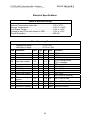
1
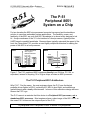
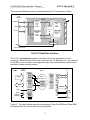
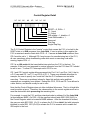
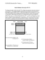
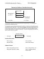
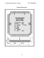
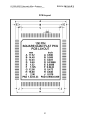
The P-51
Peripheral 8051
System on a Chip
Cybernetic Micro Systems
www.ControlChips.com
© 1999-2000 Cybernetic Micro Systems
C:\My Documents\P51chip\P51_Man5.doc
PRELIMINARY
Working Draft
05/30/00-8:51 PM
US patent and copyright law protects Cybernetic Micro Systems' hardware and
software products. This intellectual property shall remain the property of
Cybernetic Micro Systems. Duplication is subject to a license from Cybernetic
Micro Systems. Cybernetic Micro Systems reserves the right to improve design
or performance characteristics. Cybernetic Micro Systems assumes no
responsibility for the use of any circuitry other than circuitry embodied in
Cybernetic Micro Systems products. No other circuit patent licenses are implied.
Information furnished by Cybernetic Micro Systems is believed to be accurate
and reliable. However, no responsibility is assumed by Cybernetic Micro Systems
for its use, nor for any infringement of patents or other rights of third parties that
may result from its use. No license is granted by implication or otherwise under
any patent or patent right of Cybernetic Micro Systems. Further Cybernetic Micro
Systems reserves the right to revise this publication and to make changes from
time to time in the content hereof without obligation to notify any person or
organization of such revision or changes. Cybernetic Micro Systems assumes no
responsibility for any errors that may appear in this document and makes not
commitment to update the information contained herein.
Because of the wide variety of applications in which this product may be used,
Cybernetic Micro Systems makes no claim as to the product's fitness for any
given application. It is therefore the user's responsibility to ensure the safety and
viability of using this product in the user's application.
The following are trademarks and U.S. patents of Cybernetic Micro Systems,
Inc.:
Trademarks
Patents
Bin-ASCII
CY123 CY300 CY525
5,452,301
CYMPL
CY132 CY325 CY545
5,541,930
Analog-ASCII CY232 CY327 CY550
5,680,589
ASCII-Analog CY233 CY308 CY600
5,721,729
CY233-LINC
CY250 CY480 CY750
5,860,021
USB-RAM
CY251 CY500
6,021,453
P-51
CY252 CY512
© Copyright 2000 by Cybernetic Micro Systems, Inc. All rights reserved; no part
of this publication may be reproduced for distribution without the prior written
permission of
Cybernetic Micro Systems, Inc.
PO Box 3000
San Gregorio CA 94074
Tel: 650-726-3000
Fax: 650-726-3003
www.ControlChips.com
[email protected]
B
© 1999-2000 Cybernetic Micro Systems
C:\My Documents\P51chip\P51_Man5.doc
PRELIMINARY
Working Draft
05/30/00-8:51 PM
Table of Contents
Table of Contents................................................................................................... i
The P-51 Peripheral 8051 System on a Chip...................................................... 1
The P-51 Peripheral-8051 Architecture................................................................. 1
The P-51 Host Bus Interface................................................................................. 2
P-51 Pinout Diagram............................................................................................. 3
P-51 Pin List ......................................................................................................... 4
P-51 Code RAM.................................................................................................... 5
The Reset Control Register of the P-51 ................................................................ 6
P-51 Reset Behavior...................................................................................... 6
P-51 Address Space ............................................................................................. 7
Base Address Switch Settings: ............................................................................. 8
Code RAM Access:............................................................................................... 9
Host Access to the Dual Port RAM ..................................................................... 10
Chip Enable and Read/Write strobes:.......................................................... 10
Special Control Registers in Shared Memory Space: ......................................... 11
Control Register Detail........................................................................................ 12
The IRQ Control Register: .................................................................................. 13
Shared Memory Interrupt Locations:................................................................... 13
P-51 Protocol to interrupt the host: ..................................................................... 14
Host Software Interrupt of P-51: ......................................................................... 15
Summary of Software Controlled Interrupts: ....................................................... 16
Hardware Mechanism: ................................................................................. 16
Software Protocol: ....................................................................................... 16
P-51 Access to Code RAM ................................................................................. 17
Host Access to Code RAM: ................................................................................ 17
P-51 Access to Dual Port RAM: .......................................................................... 17
P-51 Dual Data Pointers: .................................................................................... 18
P-51 SQRT function............................................................................................ 19
"Debug" Features of the P-51 ............................................................................. 20
P-51 Debug Support ........................................................................................... 20
P-51 Breakpoint Processing ............................................................................... 21
Typical Breakpoint Usage ............................................................................ 21
P-51 Single-Step Processing .............................................................................. 23
Combination of Single Step and Breakpoint Operations: ............................. 24
The 8051 Ports ................................................................................................... 25
Non-Standard 8051 Port Usage.......................................................................... 25
The P-51 Instruction Set ..................................................................................... 27
ARITHMETIC OPERATIONS ...................................................................... 27
LOGICAL OPERATIONS............................................................................. 28
DATA TRANSFER....................................................................................... 29
BOOLEAN VARIABLE MANIPULATION ..................................................... 30
i
© 1999-2000 Cybernetic Micro Systems
C:\My Documents\P51chip\P51_Man5.doc
PRELIMINARY
Working Draft
05/30/00-8:51 PM
PROGRAM BRANCHING............................................................................ 30
Instructions that Affect Flag Settings (1)........................................................ 31
The P-51 Special Function Registers.................................................................. 32
Standard P-51 Special Function Registers: ................................................. 32
Additional P-51 Special Function Registers: ................................................ 33
Special P-51 Memory Locations ......................................................................... 33
Special Memory Function Locations: ........................................................... 33
The Base Address Control Register.................................................................... 34
Physical Dimensions........................................................................................... 36
PCB Layout......................................................................................................... 37
Electrical Specifications ...................................................................................... 38
Clock Circuits ...................................................................................................... 39
P-51 Demo Circuit............................................................................................... 40
ii
© 1999-2000 Cybernetic Micro Systems
C:\My Documents\P51chip\P51_Man5.doc
PRELIMINARY
Working Draft
05/30/00-8:51 PM
The P-51
Peripheral 8051
System on a Chip
For two decades the 8051 microprocessor/computer has served as the standalone
solution to countless embedded system applications. The flexibility, power, and
familiarity of the 8051 are such that 8051 knowledge is in almost every designer's tool
kit. A major weakness of the '51 is its interface to a host processor, typically either
UART-based or parallel handshake. Because these typically mismatch the speed of the
host, the Cybernetics P-51 provides a novel tightly coupled architecture for adding the
power of the 8051 to a host processor.
EISA Address Decoder &
Glue Logic &
Bidirectional buffer
OLD
HOST
386+
EISA
NEW
Host
Peripheral
HOST
386+
‘51
P-51
IRQ
RS232
PC-104
Figure 1. The P-51 peripheral 8051 interfaces directly to an ISA-bus, PC-104, or
equivalent, instead of requiring 10 to 20 glue chips, as does an 8051 processor.
The P-51 Peripheral-8051 Architecture
Why P-51? First the name. As most engineers know, the P-51 was the fastest
propeller driven fighter in WW-II, achieving 451 MPH in level flight, and exhibiting a
graceful beauty and a deadly effectiveness. In honor of this marvelous design we have
chosen the P-51 logo:
The P-51 name is a reminder that this device is a Peripheral 8051 processor, not a
standalone 8051 processor. Most engineers have a clear image of the 8051 CPU, so
the name P-51 focuses on the unique aspect of the P-51:
A peripheral 8051 requires a host to which it is peripheral.
1
© 1999-2000 Cybernetic Micro Systems
C:\My Documents\P51chip\P51_Man5.doc
PRELIMINARY
Working Draft
05/30/00-8:51 PM
This important difference is key to understanding the P-51 architecture, below:
Host
Interface
P-51
4Kx8
Dual
Port
RAM
Address
Data
ALE
DPTR
P0
256
x8
RAM
P1
Control
PC
8Kx8
Code
RAM
8051 CPU
SFR
P2
P3
IRQ
IRQ
PC-104 / EISA / uC
The P-51 Host Bus Interface
The P-51 is a peripheral processor, and thus serves as a peripheral to a host
processor. Because most of the ports, instruction set, I/O hardware, etc., are identical
to the 8052 micro controller, most engineers need only understand the new host bus
interface to begin using the device.
Host
Interface
HOST
Address
Data
IRQn
Reset
Refresh
IOChRdy
uC
P-51
Dual
Port
RAM
Code
RAM
8052
Processor
DPTR
PC
Data
RAM
P
0
SFR
P
1
P
2
IRQ ‘n’
P
3
Base
Addr
Addr | Data
Address
RD/
WR/
ALE
Figure 2. The host interface provides host access to Dual Port RAM and Code RAM
and allows the P-51 to interrupt the host using IRQs.
2
© 1999-2000 Cybernetic Micro Systems
C:\My Documents\P51chip\P51_Man5.doc
PRELIMINARY
Working Draft
05/30/00-8:51 PM
As shown in Figure 2, the host processor can access the P-51's Code RAM and Dual
Port RAM via a simple ISA bus compatible interface. The host provides a 20-bit address
and 8-bit bi-directional data bus to the P-51. The P-51 supports the EISA REFRESH &
IOCHRDY and provides a user selectable IRQ output.
P-51 Pinout Diagram
3
© 1999-2000 Cybernetic Micro Systems
C:\My Documents\P51chip\P51_Man5.doc
PRELIMINARY
Working Draft
05/30/00-8:51 PM
P-51 Pin List
Pin Name
Vdd
BClk
Pin #
1, 50, 51, 100
12, 13, 14, 63, 64,
65, 82, 95
99, 98, 97, 96, 94,
93, 92, 91
9, 8, 7, 6, 5, 4, 3, 2
90, 89, 88, 87, 86,
85, 84, 83
81, 80, 79, 78, 77,
76, 75, 74
10
RFrsh
11
Gnd
P0.0 - P0.7
P1.0 - P1.7
P2.0 - P2.7
P3.0 - P3.7
25, 24, 23, 22, 21,
20, 19, 18, 17, 16,
15
RstDrv
26
27, 28, 29, 30, 31,
32, 33, 34, 35, 36,
SA0 - SA19
37, 38, 39, 40, 41,
42, 43, 44, 45, 46
MemW
47
MemR
48
IRQ3 IRQ15
I/O Description
P 3.3 Volt Power Supply
P
8051 Port 0 (Multiplexed Data Bus and Lower
I/O Address Byte)
I/O 8051 Port 1 (General I/O)
8051 Port 2 (General I/O and Upper Address
I/O Byte)
I/O 8051 Port 3 (General I/O and Special Controls)
I
I
ISA Bus Clock, normally 8.33 MHz
ISA Refresh, high during a refresh cycle, low
during a normal cycle
O
ISA Interrupt Request signals, open drain.
No IRQ8 or IRQ13
I
ISA Reset Drive, high during system reset
I
ISA Address Bus
I
I
ISA Memory Write strobe
ISA Memory Read strobe
Chip Enable, low during ISA Read/Write
cycles, may be tied low
ISA I/O Channel Ready, open drain, low to
extend an ISA cycle
Address Latch Input, high if SA0 to SA7 are
valid as address signals, low to latch SA0 to
SA7 for multiplexed Address/Data bus (nonISA)
CE
49
I
IOChRdy
52
O
ALI
53
I
BA0 - BA3
61, 60, 59, 58, 57,
56, 55, 54
70, 69, 68, 62
XTAL1
66
I
XTAL2
67
I
Clk Out
ALE
71
72
O
O
CE Out
73
O
SD0 - SD7
Ground
I/O ISA Data Bus
I
Base Address jumper inputs
Crystal Oscillator circuit input, also external
oscillator module input
Crystal Oscillator circuit input, no connect for
oscillator module
Clock Out, P-51 oscillator circuit output clock
8051 Address Latch Enable output
Chip Enable Output, when low, all movx
instructions access external memory or devices
(inverse of P1.6 signal)
4
© 1999-2000 Cybernetic Micro Systems
C:\My Documents\P51chip\P51_Man5.doc
PRELIMINARY
Working Draft
05/30/00-8:51 PM
P-51 Code RAM
Because its operation is simplest, we discuss the P-51 Code RAM first.
As a peripheral device, the P-51 expects to be reset by the host, via a signal such as
the (E)ISA RESETDRV signal, which resets all devices at startup. While the P-51 can be
placed in reset via this hardware strobe, the P-51 will remain in the reset state until
released via a software operation, as described below. During the period while the P-51
is held in RESET:
the host has access to the P-51 Code RAM.
This is a key fact of the P-51 operation, so we repeat it.
While the P-51 is RESET, the host processor can write into the P-51's Code RAM. When
released from RESET, the P-51 executes from location 0 in Code RAM!
This is the most significant difference between a "standalone" 8051/52 and the
"peripheral" P-51. Standalone devices store code in non-volatile memory such as
EPROM, ROM, FLASH, etc. Peripheral devices store code in volatile memory, therefore
a host, or an Internet-connected device, can supply code to the P-51.
The host can access the P-51's code memory only while the P-51 is RESET.
When the P-51 executes from Code RAM, the host is locked out of Code RAM.
(The host can reset the P-51 at any time and regain access to Code RAM.)
Because most users are familiar with the 8051, and understand its "standalone"
capability (and limitation) we emphasize (still again) the differences in operation:
The host downloads code to the P-51's Code RAM while the P-51 is RESET. When the
P-51 is released from reset, it "wakes up" and immediately begins executing the
downloaded code from location zero.
5
© 1999-2000 Cybernetic Micro Systems
C:\My Documents\P51chip\P51_Man5.doc
PRELIMINARY
Working Draft
05/30/00-8:51 PM
The Reset Control Register of the P-51
The P-51 possesses a host accessible control register that is mapped into dual-port
RAM address space as described below. This control register allows the host to bring
the P-51 in and out of reset via software, as well as driving the P-51 into the reset state
via the reset pin, RSTDRV, on the P-51.
P-51 Reset Behavior
RESET-pin: The P-51 is reset when the reset pin, RSTDRV, is driven hi, and remains
in reset when the RSTDRV pin returns low.
RESET-control Register: The P-51 is reset when the least significant bit of the control
register is cleared to '0' and released from reset when this bit is set to '1'.
Control Register
0 = Reset
1 = Run
The multiple address spaces probably represent the most complex aspect of the 8051,
and the P-51 is slightly more complex. The basic 8051 address spaces are relative only
to the 8051, while a subset of the P-51 address spaces are also relative to the host.
Although each address space effectively starts at location/ address zero from the 8051
perspective, the address as seen by the host is more complicated. The complication
comes from a base address register whose contents are pin selectable (and software
selectable) that is, the base address can be specified via four pins, connected through
jumpers to ground or VCC. The high bits of the host address bus are compared to
these pins. If they match, the P-51 is chip selected by the host, and its relevant address
spaces become accessible to the host. Thus the P-51 can be mapped into the address
space of an IBM-PC class computer and can function as truly "intelligent memory".
6
© 1999-2000 Cybernetic Micro Systems
C:\My Documents\P51chip\P51_Man5.doc
PRELIMINARY
Working Draft
05/30/00-8:51 PM
P-51 Address Space
As shown in this figure:
BASE REG
USER
Specified
BASE
ADDR
BASE+0
DpRAM Space
(Shared)
FFF (=4K)
CODE RAM
BASE+1000
0
Code Space
1FFF (=(8K)
BASE+2FFF
DATA RAM
Int. Data RAM Space
0
Register Bank Space
Bit Space
Indirect Access
FF
SFR
80
FF
P2
IO and
External
Address
Space
‘movx’
P0
P3
P1
BASE + 0.
Code RAM is at
DUAL PORT RAM
0
BASE+FFF
Dual port RAM is at
IRQ
IRQ Space
Figure 3. The basic address spaces of the P-51.
7
BASE + 0x1000
(= BASE + 4096).
For example, if BASE is set to
0x0D (= 1101) then the base
address is set to 0xE4 =
11100100 which corresponds to
segment 0xE400 in an 80x86
(Real mode) segment register.
The net effect is to set the six
most significant bits from the
appropriate base address value
in the Base Table as the active
Base Address. These six bits
are compared to the six most
significant bits of the 20-bit
address applied by the host to
the P-51. When these six
address bits match, the P-51 is
selected, else the P-51 is deselected, and no access to P-51
Address space is available to
the host.
© 1999-2000 Cybernetic Micro Systems
C:\My Documents\P51chip\P51_Man5.doc
PRELIMINARY
Working Draft
05/30/00-8:51 PM
Base Address Switch Settings:
All Closed:
All Open
Switch
Settings
Segment
Address
0000
0001
0010
0011
0100
0101
0110
0111
1000
1001
1010
1011
1100
1101
1110
1111
00
A4
A8
AC
B0
B4
C8
CC
D0
D4
D8
DC
E0
E4
E8
EC
We consider three example cases in detail:
Jumper
0000
1010
0101
Base
Address
000000
110110
101101
Host Address to select P-51 Base
0000 0000 0000 0000 0000
1101 1000 0000 0000 0000
1011 0100 0000 0000 0000
The first case is the "default base" in which both the P-51 and the host addresses begin
at zero. While this may be appropriate for many embedded applications, it is typically
inappropriate for IBM-PC type applications, in which address zero for the PC is
dedicated to other functions.
In the case in which the Base address is set to '0101', the six base address bits are
'101100' which corresponds to a host address: 1011 0100 0000 0000 0000.
When the host addresses 0xB4000 the Base address of the P-51 is selected.
8
© 1999-2000 Cybernetic Micro Systems
C:\My Documents\P51chip\P51_Man5.doc
PRELIMINARY
Working Draft
05/30/00-8:51 PM
Code RAM Access:
Assume that the P-51 is attached to an (E)ISA-bus and that it's Base address jumpers
are set to '1010'. As can be read from the Base Address Table above, this selects a
Base address of 0xD8000 for the P-51 as seen by the host. Since Code RAM is at Base
+ 0x1000, to access the first byte of Code RAM, the host must put address D9000 =
D8000 + 1000 = 1101_1001_0000_0000_0000.
To access the second byte of Code RAM the host must put (hex) address 0xD9001 =
1101_1001_0000_0000_0001 on the 20 bit P-51 host address bus.
Using these addresses, the host can write 8051 binary opcodes into Code RAM that will
be executed by the P-51 when the P-51 is released from RESET. From the P-51's
perspective, the first byte of Code RAM is at location/address zero.
9
© 1999-2000 Cybernetic Micro Systems
C:\My Documents\P51chip\P51_Man5.doc
PRELIMINARY
Working Draft
05/30/00-8:51 PM
Host Access to the Dual Port RAM
As discussed above, address zero in the P-51 Code RAM is offset (hex) into host
address space by BASE + 0x1000. Thus Code read from location 0x100, as seen by
the P-51 program counter, will be written into BASE + 0x1000 + 0x100, as seen by the
host.
If this is understood, then access to the Dual Port RAM shared memory space is simple.
The first byte of dual port RAM is at the BASE address as seen by the host and at
address zero of Data Memory as seen by the P-51:
Host Address of Dual
Port Ram
P-51 Address of Dual
Port Ram, using movx
Shared Ram
BASE Î
Í0
Host Address
P-51 Address
BASE+FFF Î
Í FFF
Host Data
P-51 Data
Note that, unlike Code RAM, which is accessible only when the P-51 is RESET and the
BASE address + 1000 is presented to the P-51, the dual port RAM is accessible by the
host whenever the BASE address is presented to the P-51.
Chip Enable and Read/Write strobes:
Although the host must present an address that matches the BASE address set into the
BASE address latch, the P-51 does not actually allow access to dual port RAM (or Code
RAM) unless the Chip Enable pin (#49) is asserted low and a read or write strobe is
presented to the P-51.
10
© 1999-2000 Cybernetic Micro Systems
C:\My Documents\P51chip\P51_Man5.doc
PRELIMINARY
Working Draft
05/30/00-8:51 PM
Special Control Registers in Shared Memory Space:
Now that we know how to access shared memory space from the host, we can
understand how to access several control registers mapped into dual port RAM space.
Specifically, the first four addresses in shared memory space access control registers,
as well as dual port RAM. Thus, when the host writes to address BASE + 0, BASE + 1,
BASE + 2 or BASE + 3, the control registers are addressed (and data is also written into
dual port RAM). Similarly, the last two addresses in dual port RAM space are mapped
by special registers:
Host Addresses
Shared Memory
Space
P-51 Addresses
BASE
Control Register
0
BASE + 1
IRQ Control Reg
1
BASE + 2
Base Address Reg
2
BASE + 3
Reserved
3
Locations
BASE + 4 to
BASE + FFD
are accessed
as data by host
rd/ and wr/
strobes.
Locations
4 to FFD are
accessed as
data by P-51
rd/ and wr/
strobes.
BASE + FFE
Interrupt host
FFE
BASE + FFF
Interrupt P-51
FFF
The control registers at BASE to BASE + 3 are write-only, and can only be written by
the host. If the P-51 writes to these locations, it only writes into the dual port RAM, not
into the control registers. A read of these location returns the last data written into the
dual port RAM.
11
© 1999-2000 Cybernetic Micro Systems
C:\My Documents\P51chip\P51_Man5.doc
PRELIMINARY
Working Draft
05/30/00-8:51 PM
Control Register Detail
b7
b6
b5
b4
b3
b2
b1
b0
RESET = 0, RUN = 1
P1.1 input
P1.2 input
IRQ-enable = 1, disable = 0
Code RAM enable = 1
Reserved
Wait flag
Single Step flag
The P-51 Control Register is the "master" control that causes the P-51 to be held in the
RESET state or to RUN programs from Code RAM. If zero is written to this register the
P-51 is reset and remains reset while CR.0 = 0. If access to Code RAM is desired, then
CR.4 must be set to 1. Although CR.4 may be zero for manufacturing test of the P-51,
all user operations, either downloading code while reset or executing code while
running, require CR.4 = 1.
CR.3 is an IRQ-enable bit that can disable interrupts from the P-51 to the host. For
example, if the host is not prepared to service interrupts from the P-51 then CR.3 should
be set to zero. To allow P-51 interrupts set bit CR.3 to one.
CR.1 and CR.2 control register bits are mapped into Port 1 bit 1 and Port 1 bit 2, that is,
a P-51 can read CR.1 on P1.1 and CR.2 on P1.2. These user definable bits allow for
example, the user to specify two "mode bits" that the P-51 software can test while
executing. There are no preferred values for these bits as their value and their
meanings are completely user defined. Debug Bits CR.5, CR.6 and CR.7 are defined in
a later section, and should usually be set to zero.
Note that the Control Register does not allow individual bit access. That is, all eight bits
must be written at once. Therefore, the values written to the control register must set or
reset the desired bit while preserving the remaining bits.
For example, to reset the P-51 and then download code to address N of the Code RAM
(at host address BASE + 0x1000 + N) the user/host should write 0001 0000 (0x10) to
the Control Register which is located at BASE address. After the download is finished,
the user can write 0001 0001 (0x11) to release the P-51 from RESET (but with interrupts
inhibited) or write 0001 1001 (0x19) to release the P-51 to execute and to enable the
IRQ output to the host.
12
© 1999-2000 Cybernetic Micro Systems
C:\My Documents\P51chip\P51_Man5.doc
PRELIMINARY
Working Draft
05/30/00-8:51 PM
The IRQ Control Register:
As may be seen from the pinout diagram -- the P-51 supports numerous IRQ output
pins (IRQ-3 to IRQ-15) covering most of the IBM-PC IRQ pins of the EISA bus. These
are open collector outputs that are typically pulled up to 5 volts but can be driven low to
interrupt the host. Because IRQs are a scarce resource, only one is used by the P-51
and is selected by the host via the IRQ Control Register, mapped into location BASE +1
of the host address space.
BASE +1
b7
b6
b5
b4
b3
b2
b1
b0
0
0
0
G
x
x
x
x
IRQGate
IRQ
The low nibble is set to the desired IRQ#, for example, 0101 selects IRQ-5 while 1111
selects IRQ-15, etc. Bit G (= IRQ.4) is the Interrupt GATE which enables or disables the
IRQ (in combination with Control Register bit CR.3). The most significant bits of the
IRQ Control Register must be set to zero.
Shared Memory Interrupt Locations:
Although the IRQ control gate determines which IRQ output will be used to interrupt the
host, the actual interrupt mechanism is associated with the INTERRUPT Register at
address BASE + 0xFFE (host perspective) or equivalent address 0xFFE (P-51
perspective). When the P-51 writes to address 0xFFE in shared memory space, an
interrupt is generated and sent to the host on IRQ #N if the IRQ control register contains
0001 N and the Control Register = 0001 1xx1. The host is assumed to contain an
appropriate ISR (Interrupt Service Routine) which will read the interrupt register at
(BASE + 0xFFE) and will interpret the value read from this location. The interrupt
appearing on IRQ #N is a low going pulse. When this pulse has been generated (by the
P-51 writing to 0xFFE), all further interrupt pulses to the host are inhibited until the host
reads the (BASE +) 0xFFE location. After the host reads this location another interrupt
can be generated by the P-51, since the "lock" is removed by the read. However a P-51
program does not "know" that the interrupt has been cleared, therefore the appropriate
protocol is as follows:
13
© 1999-2000 Cybernetic Micro Systems
C:\My Documents\P51chip\P51_Man5.doc
PRELIMINARY
Working Draft
05/30/00-8:51 PM
P-51 Protocol to interrupt the host:
Host
Shared RAM
P-51
BASE + 0
00011xx1
0
BASE + 1
0 0 0 1 IRQ-N
1
BASE + FFE
Int_Req to host
FFE
(Host relative address)
(P-51 relative address)
Å P-51 writes INT_REQ
value to FFE
Host receives
INTERRUPT
Host reads
BASE + FFE
Å IRQ #N
Å (INT.REQ)
Æ P-51 reads FFE;
if non-zero, wait
Host writes zero to
BASE+FFE
Æ (zero)
Æ P-51 reads FFE;
zero indicates host ready
for next interrupt
To summarize, the host must setup the IRQ Control Register and the Master Control
Register to allow interrupts to the host on a specified IRQ-pin. Once this has been
done, the P-51 can interrupt the host by writing any (non-zero) value into address
0xFFE in shared RAM space, causing the selected IRQ-pin to pulse low. The host
should respond to this IRQ pulse by reading the value of location ( BASE + ) 0xFFE
and interpreting the value (the interpretation is by a pre-agreed convention between P51 program and host). When the host has finished and is able and willing to accept
more interrupts the host writes zero to (BASE +) 0xFFE to signal READY to the P-51.
The P-51 should test location 0xFFE for zero before writing a value to this address. If
the value is non-zero, the P-51 should wait for the value to become zero before writing a
non-zero interrupt value to 0xFFE.
14
© 1999-2000 Cybernetic Micro Systems
C:\My Documents\P51chip\P51_Man5.doc
PRELIMINARY
Working Draft
05/30/00-8:51 PM
Host Software Interrupt of P-51:
The above description details how the P-51 software can generate interrupts to the host
via an IRQ pin. The converse operation allows the host software to interrupt the P-51
by writing to location (BASE+) 0xFFF. This write will generate an interrupt on P-51 Port
3 Pin 3 (P3.3) which vectors through 8051 External Interrupt 1 location 0x13 (hex) in P51 Code RAM. The interrupt will cause P3.3 to go low and remain low until the P-51
reads location 0xFFF in shared space (dual port RAM). The act of reading 0xFFF (from
the P-51 side) clears the interrupt and P3.3 returns hi. The P-51 can interpret the value
read from 0xFFF to decide what action is being requested. Finally the P-51 can write
zero to 0xFFF, signifying to the host that the P-51 is ready to accept further interrupts.
Host
Shared RAM
P-51
BASE + 0
BASE + 1
00011xx1
0 0 0 1 IRQ-N
0
1
BASE + FFE
BASE + FFF
P-51 Intr host
Host Intr P-51
Host relative address
FFE
FFF
P-51 relative address
Host writes interrupt to BASE + FFF
to interrupt P-51:
Æ P-51 interrupted via ExtInt1,
vectors through Code RAM:0013
Æ P-51 writes zero to FFF when
ready for next interrupt from host.
Host reads BASE + FFF before next
interrupt to P-51, must be zero.
15
© 1999-2000 Cybernetic Micro Systems
C:\My Documents\P51chip\P51_Man5.doc
PRELIMINARY
Working Draft
05/30/00-8:51 PM
Summary of Software Controlled Interrupts:
dual port RAM
Interrupt Host Å
( via IRQ N )
(BASE+) FFE
(BASE+) FFF
Æ Interrupt P-51
( via ExtInt1 )
< Host Side >
< P-51 Side >
The Software Interrupts are symmetrical and are supported by P-51 hardware and
extended by software protocols.
The hardware support allows the interrupts to write to a location and thereby generate
an interrupt to the "other side". If the other side writes to the same location there is no
effect except to write a value into memory, however if the other side reads the same
location, then the effect is to clear the interrupts. When the interrupting side reads the
same location, there is no effect:
Interrupt Location
Interrupter
Æ
Interrupted
Hardware Mechanism:
Write: Interrupt
Write: No Effect
Read: No Effect
Read: Clear Interrupt
Software Protocol:
Write: Interrupt Request Value
Write: To Signal Ready (=0)
Read: see if other side is ready
Read: To decode interrupt
request value.
16
© 1999-2000 Cybernetic Micro Systems
C:\My Documents\P51chip\P51_Man5.doc
PRELIMINARY
Working Draft
05/30/00-8:51 PM
P-51 Access to Code RAM
When the P-51 is released from reset (the Control Reg must contain 0001 xxx1) its
Program Counter (PC) is set to zero. This causes the P-51 to fetch the first byte from
Code RAM and begin executing code. (Normally the first instruction is a "jump over
vectors"). During execution, the P-51 fetches all instructions from Code RAM using the
Program Counter. The P-51 has only one access mechanism to Code RAM. The 8051
"movc a,@a + Dptr" allows the P-51 to use a value in the accumulator as an index into a
table that Dptr points to, and read from the table into the accumulator. There is no
other P-51 access to Code RAM.
Host Access to Code RAM:
The host processor can, while the P-51 is held in Reset, access Code RAM at locations
BASE + 0x1000 to BASE + 0x2FFF, using normal read and write operations from the
EISA-bus side of Code RAM. There is no other host access to Code RAM.
P-51 Access to Dual Port RAM:
The P-51 uses the 8051 "movx" instruction to access its own internal dual port RAM.
Those familiar with the 8051 will remember that "movx" is normally used in conjunction
with P2 and P0 to access external memory or devices outside the 8051. This is still the
case in the P-51, however it is complicated by the existence of the integral dual port
RAM. The solution is as follows:
The P-51 I/O pin port 1.6 is used to select between dual port RAM and an external
memory or device. When P1.6 is set (as it is by 'RESET') then the P-51 "movx"
instructions address external memory (via the "CE-out" pin 73). When P1.6 is cleared,
as it is by the "clr P1.6" instruction, then "CE-out" is disabled (i.e., goes to '1') and the
internal dual port RAM is enabled. When dual port RAM is enabled, all "movx"
operations operate on dual port RAM. These include:
movx a, @ RN
movx a, @ Dptr
movx @ Rn, a
movx @ Dptr, a
;
;
;
;
read thru P2:(Rn)
read thru (Dptr)
write thru P2:(Rn)
write thru (Dptr)
17
© 1999-2000 Cybernetic Micro Systems
C:\My Documents\P51chip\P51_Man5.doc
PRELIMINARY
Working Draft
05/30/00-8:51 PM
P-51 Dual Data Pointers:
The P-51 possesses two 16-bit Data Pointers instead of the single 16-bit Dptr of the
standard 8051. These data pointers are accessed ‘one at a time’ and are selected by
setting or clearing a bit in a special function register, as follows.
The Auxiliary Data Pointer control register exists in Special Function Register space at
address 0xA2. The least significant bit, b0, of this register controls which data pointer is
in use. The data pointers are identical in behavior, although the second data pointer is
only accessible when selected and has no separate SFR location. Their utility lies in the
ability to pre-load both data pointers, then switch between them by toggling the
selection bit in the special function registers. This precludes the need, with only a single
data pointer, to point to a first location, then save the address, point to a second
location, etc. An example of the use of two data pointers to move data from a source
buffer to a destination buffer is shown below.
; CONSTANTS:
SRC_buffer = 0x400
DST_buffer = 0x500
buf_length = 0x40
; location of source bytes
; location of destination buffer
; number of bytes to move
DP_sel
; Special function register
data 0xA2
; CODE:
;
mov Dptr, # SRC_buffer
inc DP_sel
mov Dptr, # DST_buffer
mov r0, # buf_length
Copy_Loop:
;
inc
DP_sel
movx a, @ Dptr
inc
Dptr
inc
DP_sel
movx @ Dptr, a
inc
Dptr
;
djnz r0, Copy_Loop
;
…
; setup source pointer
; switch data pointers
; setup destination ptr
; switch to source pointer
; get source byte
; next source location
; switch to dest. pointer
; put byte into dest buf.
; next destination location
; repeat til done…
; fall thru with Dptr -> destination
18
© 1999-2000 Cybernetic Micro Systems
C:\My Documents\P51chip\P51_Man5.doc
PRELIMINARY
Working Draft
05/30/00-8:51 PM
P-51 SQRT function
The P-51 possesses a Square Root function that takes a 16-bit value and returns an 8bit square root. This function does not exist on any other 8051, so we describe its
operation below:
The P-51 SQRT operation utilizes special locations in the Special Function Register
address space. The 16-bit value is written into two of these locations and the 8-bit
square root is read from a third. The square root is computed in one instruction cycle, so
that the answer may be read as soon as the value has been loaded. The Special
Function Register locations involved are shown below:
Special Function Space
Reg Name
:
:
Reg Address
SQRT_lo
0x84
SQRT_hi
0x85
0x86
SQRT
:
:
The code fragment below illustrates the use the SQRT function:
SQRT_lo
SQRT_hi
SQRT
mov
mov
mov
mov
data 0x84
data 0x85
data 0x86
a, # 4
SQRT_hi, a
SQRT_lo, # 0
a, SQRT
; get hi-byte
; write hi-byte
; write lo-byte
; read answer
Note that the data can be loaded directly as an immediate (constant) value or can be
loaded from the accumulator, allowing variable data to picked up from memory and
loaded into the square root circuits. The answer can be read from the SQRT register
into the accumulator, then used as appropriate. Any direct moves to and from the
SQRT registers can be used.
19
© 1999-2000 Cybernetic Micro Systems
C:\My Documents\P51chip\P51_Man5.doc
PRELIMINARY
Working Draft
05/30/00-8:51 PM
"Debug" Features of the P-51
The classical 8051 does not support debugging with either breakpoints or single step
capability. Instead, special "bond out" versions of the chips are packaged by specialist
companies and sold as "ICE", (In-Circuit-Emulation) tools, typically for thousands of
dollars. The ICE is controlled by a host connected by an umbilical cord to the 8051
bond-out chip that is plugged into the system.
EISA
HOST
Umbilical
Cable
HOST
P-51
PC-104
8051 ICE
Classical "ICE" –
expensive kludge-based on
umbilical extension.
P-51 Debugging –
natural extension
P-51 Debug Support
The P-51 offers these features that support debugging 8051 software. None of these
features is available on standard 8051s.
•
Breakpoint operation
•
Single-step operation
Each of these features allows the user, via the host processor, to detect P-51 code
execution or data access details that are useful in debugging software. All these
features are patented or patent pending.
20
© 1999-2000 Cybernetic Micro Systems
C:\My Documents\P51chip\P51_Man5.doc
PRELIMINARY
Working Draft
05/30/00-8:51 PM
P-51 Breakpoint Processing
The 8051 has an undefined opcode, 0xA5, that has been defined as a breakpoint
instruction in the P-51. When the P-51 encounters a breakpoint instruction it copies the
address or location of the breakpoint into a mailbox in dual-port RAM, then decrements
the program counter and pushes it onto the stack, and then sets the P-51 program
counter to an address in high code RAM address space, issues an interrupt (0x2E) to
the host via IRQ, and "freezes".
BUS
CODE RAM
PC
BRKPT
STACK
PC-1
BRKPT
SERVICE
PC
RET
IRQ
Fig xxx P-51 Breakpoint processing algorithm
Typical Breakpoint Usage
Breakpoints break the flow of execution at a particular point in address space, then
typically turn control over to the user. A breakpoint is typically used to determine
whether (or when) the 8051-code execution follows a path including the breakpoint. If
multiple paths are possible, multiple breakpoints can be used. Breakpoint operation
typically requires some level of intervention, or cooperation, on the part of the user. The
P-51 allows the user to specify what actions are to occur when a breakpoint event
occurs. At a minimum, the host must replace the breakpoint with a "NOP" or must
restore the original instruction that was previously "overwritten" by the breakpoint. The
P-51 must also write at least a "return" opcode into the Breakpoint service routine in
Code RAM. The P-51 can optionally write almost any breakpoint service code
(terminated with a "return"). In this manner the P-51 can access resources, such as
data RAM contents, port I/O, accumulator, PSW, timer, contents, or any other location
or data accessible by the P-51. These resources can be copied into dual port RAM
locations by the P-51, where the host can access them (and the user can display them,
etc.). Finally, the return code at the end of the breakpoint service is encountered, and
the address of the breakpoint is popped from the stack into the P-51 program counter
register. Remember that the PC was decremented before being pushed on the stack,
so the P-51 tries to execute the instruction at the breakpoint address again! If the
21
© 1999-2000 Cybernetic Micro Systems
C:\My Documents\P51chip\P51_Man5.doc
PRELIMINARY
Working Draft
05/30/00-8:51 PM
breakpoint has been replaced by a "NOP" or by the original (pre-breakpoint) opcode,
then execution will continue normally from this location.
Summary of breakpoint operations required of the user:
PRE-BREAKPOINT:
1. Determine location in Code RAM to place breakpoint.
2. "Save" instruction at this code location.
3. Write breakpoint into code location.
4. Release P-51 from RESET.
5. P-51 runs until breakpoint executed.
POST-BREAKPOINT:
6. Host reads breakpoint address from dual port RAM mailbox (0xFFB, 0xFFC).
7. Host identifies "original" instruction at this address.
8. Host writes original instruction back into Code RAM.
9. Host writes breakpoint service routine plus "return" into high location in Code RAM.
(Base + 0x3E2F => P-51 Code Address 0x2E2F)
10. Host releases the P-51 to execute breakpoint service by clearing the Wait flag. The
Wait flag is bit 6 of the Control Register.
11. After the Wait flag is cleared, the P-51 will execute the code from address 0x2E2F
until a return instruction is encountered. The P-51 returns to the location at which
the breakpoint was originally detected, which now holds the original instruction (as
per step 8).
12. The Host can access data (if any) placed in dual port RAM by breakpoint service
processing.
13. Host options using "single step" may be employed.
22
© 1999-2000 Cybernetic Micro Systems
C:\My Documents\P51chip\P51_Man5.doc
PRELIMINARY
Working Draft
05/30/00-8:51 PM
P-51 Single-Step Processing
Breakpoints are ‘stealthy’ in that they lie unnoticed unless and until they are
encountered during the course of execution. Associated with this is the need to place
the breakpoint opcode in the code space while the host has control of the Code RAM,
that is, while the P-51 is RESET. If the host has not placed any break-points in Code
RAM, this feature is not available during the period of execution. The host can always
access Code RAM by setting the Reset bit, b0, in the Control register, but this will cause
the P-51 to begin execution again, therefore it is not generally possible to add
breakpoints to Code RAM after execution has begun.
The P-51 Single Step capability, on the other hand, allows the host to take control of the
P51 while the P-51 is executing code, with no prior preparation required. This very
useful feature is described below.
The P-51 Single Step is controlled by bit b7 of the Master Control Register, which is
located at BASE address as seen by the host. This bit is normally set to ‘0’ when the P51 is released from RESET. Because this Control register is mapped into shared
memory space, it is accessible at all times, including while the P-51 is executing code.
Thus the Single Step bit can be set to ‘1’ during P-51 execution. (Remember that the
Control Register is byte accessible, not bit accessible, so it is necessary to preserve all
of the other bits of the Control Register when setting the Single Step bit to one.) The P51 actually tests the state of the Single Step bit at then end of every instruction fetch,
proceeding as usual if the bit is zero. When the Single Step flag is set to one, the P-51
will enter the Single Step mode as follows:
The P-51, upon detecting the Single Step flag, writes the current value of the Program
Counter into the same mailbox used by the Breakpoint instruction, that is, into location
0xFFB, 0xFFC of the shared memory space. It then writes the Single Step Interrupt
value, 0x2F, to location 0xFFE, thereby generating an interrupt to the host processor.
Finally the P-51 sets bit 6 of the Control Register to ‘1’ and enters the WAIT state.
In this fashion the host can, at any time during execution, halt the P-51 and test the
mailbox to find out where the P-51 was executing when halted. This information can be
used in several ways, but we first examine the two main ways in which the P-51 is
released from the WAIT state:
The P-51 is released from the WAIT state when the host processor resets bit b6 of the
Control Register. The host can optionally reset the Single Step flag at this time or leave
the Single Step flag set to one. If the Single Step flag is reset when the WAIT-flag is
reset, then the P-51 resumes full speed execution from the location specified in the
mailbox (0xFFB,0xFFC). If the Single Step flag is left set to one when the WAIT-flag is
reset to zero, then the P-51 will execute the instruction at the location specified in the
mailbox, fetch the next instruction, test the Single Step flag, and, finding it set to one,
23
© 1999-2000 Cybernetic Micro Systems
C:\My Documents\P51chip\P51_Man5.doc
PRELIMINARY
Working Draft
05/30/00-8:51 PM
will again execute the operations described above for the Single Step procedure. In this
manner, the P-51 can be made to single step through its code, interrupting the host at
every step, and telling the host, via the mailbox, where the next instruction is located.
Combination of Single Step and Breakpoint Operations:
Once the P-51 has seen the Single Step flag and entered the WAIT state, it will remain
there until the host resets the WAIT-flag, b6. While the P-51 waits, the host can access
the P-51 Code RAM just as if the P-51 were held in RESET. However, unlike the case of
RESET, the P-51 will not begin executing at location zero, but will execute from the
location specified in the mailbox. This is a major difference, and allows the host to
combine the Breakpoint features with the Single Step features to achieve a very
powerful debug capability. In particular, the host can reach into Code RAM, pick up the
instruction about to be executed, save this instruction, and replace it with the breakpoint
opcode. If the host then clears the WAIT-flag, the P-51 will execute the breakpoint
instruction, and generate a breakpoint interrupt (with or without the Single Step flag set!)
This breakpoint interrupt service can then be used to access P-51 resources as
described in the section on Breakpoint behavior. In this way the host can break into P51 execution at arbitrary times, and gain control of the P-51 processor in a way not
possible with standard 8051s, and more flexibly even than most ICEs.
24
© 1999-2000 Cybernetic Micro Systems
C:\My Documents\P51chip\P51_Man5.doc
PRELIMINARY
Working Draft
05/30/00-8:51 PM
The 8051 Ports
The standard 8051 ports are reproduced in the P-51. All four ports are bi-directional
eight bit ports with individually SET'able and CLR'able pins, that can be read or written as
an eight bit port or can be treated as eight individual I/O lines in any combination, 5 in, 3
out, etc. With the exception of P1.1, P1.2, P1.6, and the External Interrupt (P3.3),
discussed later, all of the pins are functionally identical to the 8051 micro controller. In
addition, P-51 ports have the special functions associated with 8051 ports, that is, P0
serves as multiplexed address and data port, and P2 provides the associated high
address bits for "movx" instructions. The Address Latch Enable (ALE) pin serves to
latch the low address from P0 and the RD/ and WR/ pins (P3.6 and P3.7) read or write
data to or from P0. Other P3 pins provide UART functionality, counter/timer interface,
and external interrupt capability.
P2
HI ADDR
ALE
P0
P3
LO ADDR
DATA
RD/ (P3.6)
WR/ (P3.7)
Figure 4. The P-51 supports 8051 "movx" instructions.
Non-Standard 8051 Port Usage
Four 8051 Port pins are not used in their standard way by the P-51. They are P1.1,
P1.2, P1.6, and P3.3.
The inputs to port pins P1.1 and P1.2 are specified by Control Register bits 1 and 2, as
discussed in the section describing the Control Register (Host Relative Address BASE +
0). This allows the host software to optionally control the execution of P-51 code, by
selecting various combinations of these two bit values. Note that both the host and the
25
© 1999-2000 Cybernetic Micro Systems
C:\My Documents\P51chip\P51_Man5.doc
PRELIMINARY
Working Draft
05/30/00-8:51 PM
P-51 software must agree on the interpretation of these bit values. They are not
predefined in any way by the P-51 device. Also, the bit values read by the P-51 are the
inverse of the bit values written into the Control Register. In this way, a reset, in which
the Control Register bits are cleared to zero, will drive the P1.1 and P1.2 bits of the P51 to a one value.
If the P-51 software writes to bits P1.1 and P1.2, the values written will be output on the
actual P-51 port pins P1.1 and P1.2 (device pins 8 and 7). The values read by the P-51
will still be the values from the Control Register. This means that P1.1 and P1.2 do not
have the normal bi-directional I/O behavior of standard 8051 ports. Rather these bits
have separate outputs (P1.1 and P1.2 device pins) and separate inputs (Control
Register bits).
P-51 port pin P1.6 is used to select between the integral dual port RAM and external
devices, as explained in the section P-51 Access to Dual Port RAM. When this bit is
cleared by the P-51 software, the integral dual port RAM is enabled, and when this bit is
set, external devices are enabled.
As a convenience in selecting the external device, the P-51 also generates the CE Out
signal, which is the inverse of the P1.6 pin. Most devices use an active-low chip enable
signal, so the CE Out signal allows you to directly connect an external device to the P51, without the need for an external inverter! Use of these pins for the hardware
selection of an external device is optional. However, P1.6 must always be cleared to
allow the P-51 software to access the integral dual port RAM, and set to allow access to
an external device.
Finally, port pin P3.3 is reserved for use as the interrupt to the P-51 from the integral
dual port RAM. When the host software writes to dual port RAM location 0xFFF, this
generates an interrupt to the P-51. That interrupt comes to the P-51 through internal
logic to the P-51 ExtInt1 interrupt. If the P-51 software has enabled External Interrupt 1,
this dual port RAM interrupt causes the P-51 to go to the ExtInt1 interrupt vector at
location 0x13 of the P-51 code space. The interrupt signal is removed when the P-51
software reads the dual port RAM location 0xFFF to see what code was written by the
host.
Normal applications of the P-51 should not use P3.3 for any purpose except as the dual
port RAM interrupt. The port 3 register bit P3.3 should be kept high (the reset default)
to allow the dual port RAM interrupt signal to properly drive the internal ExtInt1 signal. If
this bit is driven to zero by P-51 software, the ExtInt1 signal will always be low, and will
no longer indicate the interrupt request from the dual port RAM.
26
© 1999-2000 Cybernetic Micro Systems
C:\My Documents\P51chip\P51_Man5.doc
PRELIMINARY
Working Draft
05/30/00-8:51 PM
The P-51 Instruction Set
All 8051 instructions are executed by the P-51. These are listed below:
ARITHMETIC OPERATIONS
Mnemonic
Description
Byte
ADD
ADD
ADD
ADD
ADDC
ADDC
ADDC
ADDC
SUBB
SUBB
SUBB
SUBB
A,Rn
A,direct
A,@Ri
A,#data
A,Rn
A,direct
A,@Ri
A,#data
A,Rn
A,direct
A,@Ri
A,#data
1
2
1
2
1
2
1
2
1
2
1
2
INC
INC
INC
INC
DEC
DEC
DEC
DEC
INC
MUL
DIV
DA
A
Rn
direct
@Ri
A
Rn
direct
@Ri
DPTR
AB
AB
A
Add register to Accumulator
Add direct byte to Accumulator
Add indirect RAM to Accumulator
Add immediate data to Accumulator
Add register to Accumulator with Carry
Add direct byte to Accumulator with Carry
Add indirect RAM to Accumulator with Carry
Add immediate data to Acc with Carry
Subtract Register from Acc with borrow
Subtract direct byte from Acc with borrow
Subtract indirect RAM from Acc with borrow
Subtract immediate data from Acc with
borrow
Increment Accumulator
Increment register
Increment direct byte
Increment direct RAM
Decrement Accumulator
Decrement Register
Decrement direct byte
Decrement indirect RAM
Increment Data Pointer
Multiply A & B
Divide A by B
Decimal Adjust Accumulator
Oscil.
Period
12
12
12
12
12
12
12
12
12
12
12
12
1
1
2
1
1
1
2
1
1
1
1
1
12
12
12
12
12
12
12
12
12 (24)
24 (48)
24 (48)
12
All Mnemonics copyrighted ©Intel Corporation 1980
27
Where P-51 timing differs
from the original 8051, the
8051 timing is shown in
parentheses.
© 1999-2000 Cybernetic Micro Systems
C:\My Documents\P51chip\P51_Man5.doc
PRELIMINARY
Working Draft
05/30/00-8:51 PM
LOGICAL OPERATIONS
Mnemonic
Description
Byte
ANL
ANL
ANL
ANL
ANL
ANL
ORL
ORL
ORL
ORL
ORL
ORL
XRL
XRL
XRL
A,Rn
A,direct
A,@Ri
A,#data
direct,A
direct,#data
A,Rn
A,direct
A,@Ri
A,#data
direct,A
direct,#data
A,Rn
A,direct
A,@Ri
1
1
1
2
2
3
1
2
1
2
2
3
1
2
1
XRL
A,#data
2
12
XRL
XRL
direct,A
direct,#data
2
3
12
24
CLR
CPL
RL
RLC
A
A
A
A
1
1
1
1
12
12
12
12
RR
RRC
A
A
AND Register to Accumulator
AND direct byte to Accumulator
AND indirect RAM to Accumulator
AND immediate data to Accumulator
AND Accumulator to direct byte
AND immediate data to direct byte
OR register to Accumulator
OR direct byte to Accumulator
OR indirect RAM to Accumulator
OR immediate data to Accumulator
OR Accumulator to direct byte
OR immediate data to direct byte
Exclusive-OR register to Accumulator
Exclusive-OR direct byte to Accumulator
Exclusive-OR indirect RAM to
Accumulator
Exclusive-OR immediate data to
Accumulator
Exclusive-OR Accumulator to direct byte
Exclusive-OR immediate data to direct
byte
Clear Accumulator
Complement Accumulator
Rotate Accumulator Left
Rotate Accumulator Left through the
Carry
Rotate Accumulator Right
Rotate Accumulator Right through the
Carry
Oscil.
Period
12
12
12
12
12
24
12
12
12
12
12
24
12
12
12
1
1
12
12
SWAP
A
Swap nibbles within the Accumulator
1
12
All Mnemonics copyrighted ©Intel Corporation 1980
28
© 1999-2000 Cybernetic Micro Systems
C:\My Documents\P51chip\P51_Man5.doc
PRELIMINARY
Working Draft
05/30/00-8:51 PM
DATA TRANSFER
Mnemonic
Description
Byte
MOV
MOV
MOV
MOV
MOV
MOV
MOV
MOV
MOV
MOV
MOV
MOV
MOV
MOV
MOV
MOV
MOVC
MOVC
MOVX
MOVX
MOVX
MOVX
PUSH
POP
XCH
XCH
XCH
A,Rn
A,direct
A,@Ri
A,#data
Rn,A
Rn,direct
Rn,#data
direct,A
direct,Rn
direct,direct
direct,@Ri
direct,#data
@Ri,A
@Ri,direct
@Ri,#Data
DPTR,#data16
A,@A+DPTR
A,@A+PC
A,@Ri
A,@DPTR
?@Ri,A
?@DPTR,A
Direct
Direct
A,Rn
A,direct
A,@Ri
1
2
1
2
1
2
2
2
2
3
2
3
1
2
2
3
1
1
1
1
1
1
2
2
1
2
1
XCHD
A,@Ri
Move register to Accumulator
Move direct byte to Accumulator
Move indirect RAM to Accumulator
Move immediate data to Accumulator
Move Accumulator to register
Move direct byte to register
Move immediate data to register
Move Accumulator to direct byte
Move register to direct byte
Move direct byte to direct
Move indirect RAM to direct byte
Move immediate data to direct byte
Move Accumulator to indirect RAM
Move direct byte to indirect RAM
Move immediate data to indirect RAM
Load Data Pointer with 16-bit constant
Move Code byte relative to DPTR to Acc
Move Code byte relative to PC to Acc
Move External RAM (8-bit addr) to Acc
Move External RAM (16-bit addr) to Acc
Move Acc to External RAM (8-bit addr)
Move Acc to External RAM (16-bit addr)
Push direct byte onto stack
Pop direct byte from stack
Exchange register with Accumulator
Exchange direct byte with Accumulator
Exchange indirect RAM with
Accumulator
Exchange low-order Digit indirect RAM
with Acc
Oscil.
Period
12
12
12
12
12
24
12
12
12 (24)
24
12 (24)
24
12
24
12
24
24
24
24
24
24
24
24
12 (24)
12
12
12
1
12
All Mnemonics copyrighted ©Intel Corporation 1980
29
© 1999-2000 Cybernetic Micro Systems
C:\My Documents\P51chip\P51_Man5.doc
PRELIMINARY
Working Draft
05/30/00-8:51 PM
BOOLEAN VARIABLE MANIPULATION
Mnemonic
Description
Byte
CLR
CLR
SETB
SETB
CPL
CPL
ANL
ANL
ORL
ORL
MOV
MOV
JC
JNC
JB
JNB
JBC
Clear Carry
Clear direct bit
Set Carry
Set direct bit
Complement Carry
Complement direct bit
AND direct bit to Carry
AND complement of direct bit to Carry
OR direct bit to Carry
OR complement of direct bit to Carry
Move direct bit to Carry
Move Carry to direct bit
Jump if Carry is set
Jump if Carry not set
Jump if direct Bit is set
Jump if direct Bit is Not set
Jump if direct Bit is set & clear bit
1
2
1
2
1
2
2
2
2
2
2
2
2
2
3
3
3
C
bit
C
bit
C
Bit
C,bit
C,/bit
C,bit
C,/bit
C,bit
bit,C
Rel
Rel
bit,rel
bit,rel
bit,rel
Oscil.
Period
12
12
12
12
12
12
12 (24)
12 (24)
12 (24)
12 (24)
12
12 (24)
24
24
24
24
24
PROGRAM BRANCHING
Mnemonic
Description
Byte
ACALL
LCALL
RET
RETI
AJMP
LJMP
SJMP
JMP
JZ
JNZ
CJNE
addr11
addr16
rel
@A+DPTR
rel
rel
A,direct,rel
2
3
1
1
2
3
2
1
2
2
3
CJNE
A,#data,rel
3
24
CJNE
Rn,#data,rel
3
24
CJNE
@Ri,#data,rel
3
24
DJNZ
DJNZ
Rn,rel
direct,rel
Absolute Subroutine Call
Long Subroutine Call
Return from Subroutine
Return from interrupt
Absolute Jump
Long Jump
Short Jump (relative addr)
Jump indirect relative to the DPTR
Jump if Accumulator is Zero
Jump if Accumulator is Not Zero
Compare direct byte to Acc and Jump if
Not Equal
Compare Immediate to Acc and Jump if
Not Equal
Compare immediate to register and
Jump if Not Equal
Compare immediate to indirect and
Jump if Not Equal
Decrement register & Jump if Not Zero
Decrement direct byte and Jump if Not
Zero
No Operation
Oscil.
Period
24
24
24
24
24
24
24
12 (24)
24
24
24
2
3
24
24
1
12
NOP
addr11
addr16
All Mnemonics copyrighted ©Intel Corporation 1980
30
© 1999-2000 Cybernetic Micro Systems
C:\My Documents\P51chip\P51_Man5.doc
PRELIMINARY
Working Draft
05/30/00-8:51 PM
Instructions that Affect Flag Settings (1)
Instruction
Flag
Instruction
Flag
C
OV
AC
C
OV
AC
ADD
X
X
X
CLR C
0
ADDC
X
X
X
CPL C
X
SUBB
X
X
X
ANL C,bit
X
MUL
0
X
ANL C,/bit
X
DIV
0
X
ORL C,bit
X
DA
X
ORL C,bit
X
RRC
X
MOV C,bit
X
RLC
X
CJNE
X
SETB C
1
(1)
Note that operations on SFR byte address 208 or bit addresses 209-215 (i.e., the PSW or bits
in the PSW) will also affect flag settings.
Note on instruction set and addressing modes:
Rn
— Register R7-R0 of the currently selected Register Bank.
direct
— 8-bit internal data location's address. This could be an Internal Data RAM
location (0-127) or a SFR [i.e., I/O port, control register, status register, etc. (128255)].
@Ri
— 8-bit internal data RAM location (0-255) addressed indirectly through register R1
or R0.
#data
— 8-bit constant included in instruction.
#data 16 — 16-bit constant included in instruction.
addr 16
— 16-bit destinationaddress. Used by LCALL & LJMP. A branch can be anywhere
within the 64K-byte Program Memory address space.
addr 11
— 11-bit destination address. Used by ACALL & AJMP. The branch will be within
the same 2K-byte page of program memory as the first byte of the following
instruction.
rel
— Signed (two's complement) 8-bit offset byte. Used by SJMP and all conditional
jumps. Range is -128 to +127 bytes relative to first byte of the following
instruction.
bit
— Direct Addressed bit in Internal Data RAM or Special Function Register.
31
© 1999-2000 Cybernetic Micro Systems
C:\My Documents\P51chip\P51_Man5.doc
PRELIMINARY
Working Draft
05/30/00-8:51 PM
The P-51 Special Function Registers
Single chip micro-controllers differ from microprocessors, in that they possess
peripheral interface components and controller-oriented hardware "on a chip". For
example, the 8051 supports timers, counters, UARTs, interrupt pins, I/O ports, and
memory on a single chip, whereas most microprocessors require external UART,
external counter/timer, external interrupt support chips and external memory. The first
true single chip controller, Intel's 8048, contained this special hardware, and a set of
instructions, such as "START Time" to control the hardware. The 8051 advanced the
state of the art considerably, by mapping all of the special purpose hardware into a
"special function register" file, which could be accessed by both bit and byte
instructions. This not only organized the I/O nicely, but, by using "mov" instructions and
"clr bit" and "set bit" instructions to control the I/O hardware, it eliminated the need for
special instructions, thereby freeing up the opcode space for more general instructions.
The P-51 supports all 8052 special function registers.
Standard P-51 Special Function Registers:
Symbol
ACC
B
PSW
SP
DPTR
DPL
DPH
P0
P1
P2
P3
IP
IE
TMOD
TCON
T2CON
TH0
TL0
TH1
TL1
TH2
TL2
RCAP2H
RCAP2L
SCON
SBUF
PCON
Description
Accumulator
B Register
Program Status Word
Stack Pointer
Data Pointer 2 bytes
Low Byte
High Byte
Port 0
Port 1
Port 2
Port 3
Interrupt Priority Control
Interrupt Enable Control
Timer/Counter Mode Control
Timer/Counter Control
Timer/Counter 2 Control
Timer/Counter 0 High Byte
Timer/Counter 0 Low Byte
Timer/Counter 1 High Byte
Timer/Counter 1 Low Byte
Timer/Counter 2 High Byte
Timer/Counter 2 Low Byte
T/C 2 Capture Reg High Byte
T/C 2 Capture Reg Low Byte
Serial Control
Serial Data Buffer
Power Control
32
Address
0xE0
0xF0
0xD0
0x81
0x82
0x83
0x80
0x90
0xA0
0xB0
0xB8
0xA8
0x89
0x88
0xC8
0x8C
0x8A
0x8D
0x8B
0xCD
0xCC
0xCB
0xCA
0x98
0x99
0x87
© 1999-2000 Cybernetic Micro Systems
C:\My Documents\P51chip\P51_Man5.doc
PRELIMINARY
Working Draft
05/30/00-8:51 PM
In addition to the standard 8052 special function registers, the P-51 implements a few
additional registers. The additional registers are shown below:
Additional P-51 Special Function Registers:
Symbol
SQRT_lo
SQRT_hi
SQRT
DP_sel
Description
Square Root data low byte
Square Root data high byte
Square Root result
Dual Data Pointer Select
Address
0x84
0x85
0x86
0xA2
Special P-51 Memory Locations
The following locations in the P-51 memory space are used for special functions. They
are discussed in other sections of this manual, and are summarized here.
Special Memory Function Locations:
Host Relative
Address
Function
P-51
Relative
Addr
BASE + 0x0000
Control Register
xxxx
BASE + 0x0001
IRQ Control Reg
xxxx
BASE + 0x0002
Base Address Reg
xxxx
BASE + 0x0003
Reserved
xxxx
BASE + 0x0FFB
Mail Box Lo Byte
BASE + 0x0FFC Mail Box Hi Byte
BASE + 0x0FFE
Interrupt Host
BASE + 0x0FFF
Interrupt P51
BASE + 0x3E2F
Breakpoint
Subroutine
Notes
Host access only, P51 can only
access dpRAM
Host access only, P51 can only
access dpRAM
Host access only, P51 can only
access dpRAM
Host access only, P51 can only
access dpRAM
Data
0x0FFB
Data
0x0FFC
Low byte of break point and
single step address
High byte of break point and
single step address
Data
0x0FFE
Data
0x0FFF
P51 write interrupts host. Host
read clears interrupt
Host write interrupts P51. P51
read clears interrupt
Code
0x2E2F
Start of P51 Subroutine executed
after a breakpoint
33
© 1999-2000 Cybernetic Micro Systems
C:\My Documents\P51chip\P51_Man5.doc
PRELIMINARY
Working Draft
05/30/00-8:51 PM
The Base Address Control Register
Another special control register is the Base Address Control Register, mapped into
location BASE + 2 of the host address space. This register allows the host to
dynamically change the base address of the P-51 through software control.
As indicated previously in the Base Address Settings section, one of 16 base addresses
may be selected for the P-51, by properly setting the values on the four Base Address
signals, BA0 to BA3. These settings map to 16 specific segment addresses, specified
by the bit pattern on the upper 6 address lines, SA14 to SA19. However, with 6 bits, it
is possible to specify up to 64 possible combinations, so the Base Address signals only
allow you to select one quarter of the possible addresses. We have selected the most
useful 16 addresses, based on a standard PC architecture, where the lower 640K bytes
of the address space are dedicated to system memory, and the upper 384K bytes are
shared among the system BIOS, video memory, and special adapters, such as the P51.
After a hardware reset, from the RstDrv signal, the P-51 base address is always set
from the values of the Base Address signals, to the selected one of 16 addresses.
Once this base address is known, host software can access the Base Address Control
Register, at the current BASE + 2, to change the base address to another value. By
writing to the Base Address Control Register, host software has access to all 6 upper
address bits, and can select any of the 64 possible Base Addresses. The format for the
Base Address Control Register is shown below:
BASE ADDR
b7
b6
b5
b4
b3
b2
b1
b0
x
x
x
x
x
x
0
0
Note that the upper 6 bits of the register correspond to the upper 6 address lines of the
desired address pattern. Host software would write the desired segment address into
this register to select the desired base address. For example, to select a base address
of 0xD4000 (1101 0100 0000 0000 0000), host software would write 0xD4 into the Base
Address Control Register. Also note that the two least significant bits of this register
must always be 00.
The Base Address Control Register is most useful for selecting base addresses that
cannot be selected by the Base Address signals, but may also be used to select the
same addresses as the Base Address signals, as shown above, with the 0xD4 example.
Examples of base addresses that are not selectable by the external signals would be
0xC4, 0xB8, 0xA0, and any address between 0x00 and 0xA4. However, you must
verify that the desired base address is available within the memory space of your
system, and is not being used by another device or system memory. If there is a
conflict between multiple devices, it is possible that the P-51 cannot be accessed at that
address.
34
© 1999-2000 Cybernetic Micro Systems
C:\My Documents\P51chip\P51_Man5.doc
PRELIMINARY
Working Draft
05/30/00-8:51 PM
Since inadvertent writes to the Base Address Control Register can have severe
consequences, possibly making the P-51 device inaccessible to the host software, write
access to this register is protected by a 5 step sequence. All steps must be taken in the
proper sequence to successfully change the P-51 base address. Also, the P-51 base
address should only be changed while the P-51 is being held in reset, through the main
Control Register, at BASE + 0. This is shown as step 0 of the sequence below, but is
not required if the P-51 is still in the reset state from a system hardware reset. The
steps for changing the P-51 base address are:
0. Write 0x00 (0000 0000) to the Control Register at the current BASE + 0
1. Write 0x40 (0100 0000) to the IRQ Control Register, at the current BASE + 1
2. Write the desired new base address value to the Base Address Control Register, at
the current BASE + 2
3. Write 0x80 (1000 0000) to the IRQ Control Register, at the current BASE + 1
4. Again, write the new base address value to the BASE Address Control Register, at
the current BASE + 2
5. Now write 0x10 (0001 0000) to the Control Register at the new BASE + 0
The final step provides host software with access to the P-51 Code RAM, so the desired
program can be downloaded before the P-51 is released from reset. Host software
should also select the desired interrupt, by writing the proper value to the IRQ Control
Register, at the new BASE + 1, since the above sequence disables any interrupt
selection.
The P-51 may now be used at the new base address, and will stay at that base address
until either 1) a hardware reset, for which the base address will become that selected by
the Base Address input signals, or 2) until the host software changes the base address
again, through the Base Address Control Register.
35
© 1999-2000 Cybernetic Micro Systems
C:\My Documents\P51chip\P51_Man5.doc
PRELIMINARY
Working Draft
Physical Dimensions
36
05/30/00-8:51 PM
© 1999-2000 Cybernetic Micro Systems
C:\My Documents\P51chip\P51_Man5.doc
PRELIMINARY
Working Draft
PCB Layout
37
05/30/00-8:51 PM
© 1999-2000 Cybernetic Micro Systems
C:\My Documents\P51chip\P51_Man5.doc
PRELIMINARY
Working Draft
05/30/00-8:51 PM
Electrical Specifications
Absolute Maximum Ratings
Ambient Temperature under bias................................ 0ºC to 70ºC
Storage Temperature.................................................. -55ºC to +125ºC
Vdd Supply Voltage .................................................... -0.3V to +4.0V
Voltage on any I/O pin with respect to GND ............... -0.3V to +6.0V
Power Dissipation ....................................................... 500 mW
DC and Operating Characteristics
Temperature Range .................... 0ºC to 70ºC
Vdd Supply Voltage ..................... +3.0V to +3.6V
Sym Parameter
Icc
pwr supply current
Min
Vih
input high voltage
Vil
Iih
Iil
Voh
Vol
input low voltage
input high current
input low current
output high voltage
output low voltage
Ioz
Ipu
Fcy
Fos
Tri-state leakage
current
Pull-up current
crystal frequency
oscillator frequency
Typ
46
20
16
Max
80
40
35
Unit
mA
mA
mA
2.0
5.5
V
-0.2
-10
-10
2.4
0.8
+10
+10
0.4
0.4
V
uA
uA
V
V
V
Remarks
60 MHz
40 MHz
11 MHz
5 Volt tolerant inputs,
TTL compatible
TTL compatible
Vin = Vdd
Vin = GND
Ioh = -4 mA
Iol = 4 mA
Iol = 8 mA on IoChRdy
+10
uA
Vin = GND to Vdd
160
51
60
uA
MHz
MHz
Vin = GND, R ~ 50K ohm
see clock circuits
see clock circuits
10
22
4
1
66
38
© 1999-2000 Cybernetic Micro Systems
C:\My Documents\P51chip\P51_Man5.doc
PRELIMINARY
Working Draft
05/30/00-8:51 PM
Clock Circuits
The P-51 may operate with
crystal or external clock circuits,
as shown in the clock figures. An
external oscillator in the range of
1 to 60 MHz may be used on
XTAL1, and must use the same
VDD voltage as the P-51.
XTAL2
+3.3V
P- 51
CRYSTAL
OSCILLATOR
1-60 MHz
XTAL1
The frequency range for the
crystal circuit is 4 to 51 MHz. The
circuitry is slightly different for
fundamental vs. third-overtone
crystals. The boundary between
fundamental and third overtone
crystals is approximately 26 MHz
and should be verified with the
crystal manufacturer.
Crystal Oscillator Circuit
XTAL2
5-30pF
0-200 Ω
XTAL
<26 MHz
P- 51
As with standard 8051 devices,
the internal P-51 serial baud
rates assume an 11.059 MHz
crystal and multiples thereof.
1M Ω
XTAL1
5-30pF
Fundamental Crystal Circuit
XTAL2
5-30pF
0-200 Ω
XTAL
>26 MHz
P- 51
5-30pF
1M Ω
XTAL1
0.01uF
3.3uH
Third Overtone Crystal Circuit
39
© 1999-2000 Cybernetic Micro Systems
C:\My Documents\P51chip\P51_Man5.doc
PRELIMINARY
Working Draft
P-51 Demo Circuit
40
05/30/00-8:51 PM