Download OPMM-1616-XT User Manual
Transcript
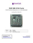
RUBY-MM-1616 Family
PC/104 I/O Module with 4, 8 or 16 16-bit Analog Outputs and 48 GPIO
Rev A.0 June 2013
Revision
Date
A.0
6/13/2013
FOR TECHNICAL SUPPORT
PLEASE CONTACT:
[email protected]
Comment
Initial release
Copyright 2013
Diamond Systems Corporation
555 Ellis Street
Mountain View, CA 94043 USA
Tel 1-650-810-2500
Fax 1-650-810-2525
www.diamondsystems.com
TABLE OF CONTENTS
1.
2.
Important Safe Handling Information .............................................................................................................3
Introduction .......................................................................................................................................................4
2.1 Description .....................................................................................................................................................4
2.2 Features .........................................................................................................................................................4
2.3 Available Models............................................................................................................................................5
3. Functional Overview .........................................................................................................................................5
3.1 Functional Block Diagram ..............................................................................................................................5
3.2 Board Drawing ...............................................................................................................................................6
4. Connector Pinout ..............................................................................................................................................7
4.1 PC/104 (J1, J2) ..............................................................................................................................................7
4.2 PC/104-Plus PCI Bus Connector (J3) ...........................................................................................................8
4.3 Analog Output (J4) ........................................................................................................................................9
4.4 Digital I/O (J5) ............................................................................................................................................. 10
4.5 HART Programming Connector (J9) .......................................................................................................... 10
5. Board Configuration ...................................................................................................................................... 11
5.1 Base Address ............................................................................................................................................. 11
5.2 IRQ Selection.............................................................................................................................................. 11
5.3 Digital I/O Logic Level ................................................................................................................................. 11
5.4 Digital I/O Pull-Up/Down ............................................................................................................................. 11
5.5 PCI Slot ID .................................................................................................................................................. 12
5.6 Auto Bus Select .......................................................................................................................................... 12
5.7 D/A Converter Power On Clear .................................................................................................................. 12
6. Theory of Operation....................................................................................................................................... 13
6.1 Analog Functionality ................................................................................................................................... 13
6.1.1
D/A Functions .................................................................................................................................... 13
6.1.2
Waveform Generator Circuit .............................................................................................................. 13
6.1.3
D/A Calibration ................................................................................................................................... 13
6.2 Digital I/O Functionality ............................................................................................................................... 14
6.2.1
Digital I/O ........................................................................................................................................... 14
6.2.2
Counter/Timers .................................................................................................................................. 14
6.2.3
Pulse Width Modulators ..................................................................................................................... 14
7. Register MAP.................................................................................................................................................. 15
7.1 I/O Map Summary....................................................................................................................................... 15
7.2 PCI Configuration Space Usage................................................................................................................. 16
7.3 D/A Block (page 1)...................................................................................................................................... 17
7.4 Digital I/O Block (page 2) ............................................................................................................................ 18
7.5 Counter and PWM Block (page 3) .............................................................................................................. 19
7.6 EEPROM Block (page 5) ............................................................................................................................ 19
7.7 Interrupt, Configuration, and ID Registers Block (page 7).......................................................................... 20
7.8 Capabilities Readback Registers and Page Control Block (page 15) ........................................................ 20
8. D/A Circuit ...................................................................................................................................................... 21
9. Waveform Generator ..................................................................................................................................... 23
10. EEPROM Interface ......................................................................................................................................... 25
11. Digital I/O ........................................................................................................................................................ 26
12. Counters/Timers ............................................................................................................................................ 28
13. Pulse Width Modulation ................................................................................................................................ 29
14. Miscellaneous Funtions ................................................................................................................................ 30
15. Internal Signals and Functions .................................................................................................................... 30
15.1 Interrupts ..................................................................................................................................................... 30
15.2 EEPROM Reload ........................................................................................................................................ 31
15.3 Reset .......................................................................................................................................................... 31
16. Bus Interface .................................................................................................................................................. 32
17. Specifications................................................................................................................................................. 33
RMM-1616AP-XT User Manual Rev A.0
www.diamondsystems.com
Page 2
1. IMPORTANT SAFE HANDLING INFORMATION
WARNING!
ESD-Sensitive Electronic Equipment
Observe ESD-safe handling procedures when working with this product.
Always use this product in a properly grounded work area and wear appropriate
ESD-preventive clothing and/or accessories.
Always store this product in ESD-protective packaging when not in use.
Safe Handling Precautions
This board contains a high density connector with many connections to sensitive electronic components. This
creates many opportunities for accidental damage during handling, installation and connection to other
equipment. The list here describes common causes of failure found on boards returned to Diamond Systems for
repair. This information is provided as a source of advice to help you prevent damaging your Diamond (or any
vendor’s) embedded computer boards.
ESD damage – This type of damage is usually almost impossible to detect, because there is no visual sign of
failure or damage. The symptom is that the board eventually simply stops working, because some component
becomes defective. Usually the failure can be identified and the chip can be replaced. To prevent ESD damage,
always follow proper ESD-prevention practices when handling computer boards.
Damage during handling or storage – On some boards we have noticed physical damage from mishandling. A
common observation is that a screwdriver slipped while installing the board, causing a gouge in the PCB surface
and cutting signal traces or damaging components.
Another common observation is damaged board corners, indicating the board was dropped. This may or may not
cause damage to the circuitry, depending on what is near the corner. Most of our boards are designed with at
least 25 mils clearance between the board edge and any component pad, and ground / power planes are at least
20 mils from the edge to avoid possible shorting from this type of damage. However these design rules are not
sufficient to prevent damage in all situations.
A third cause of failure is when a metal screwdriver tip slips, or a screw drops onto the board while it is powered
on, causing a short between a power pin and a signal pin on a component. This can cause overvoltage / power
supply problems described below. To avoid this type of failure, only perform assembly operations when the
system is powered off.
Sometimes boards are stored in racks with slots that grip the edge of the board. This is a common practice for
board manufacturers. However our boards are generally very dense, and if the board has components very close
to the board edge, they can be damaged or even knocked off the board when the board tilts back in the rack.
Diamond recommends that all our boards be stored only in individual ESD-safe packaging. If multiple boards are
stored together, they should be contained in bins with dividers between boards. Do not pile boards on top of each
other or cram too many boards into a small location. This can cause damage to connector pins or fragile
components.
Power supply wired backwards – Our power supplies and boards are not designed to withstand a reverse
power supply connection. This will destroy each IC that is connected to the power supply (i.e. almost all ICs). In
this case the board will most likely will be unrepairable and must be replaced. A chip destroyed by reverse power
or by excessive power will often have a visible hole on the top or show some deformation on the top surface due
to vaporization inside the package. Check twice before applying power!
Overvoltage on digital I/O line – If a digital I/O signal is connected to a voltage above the maximum specified
voltage, the digital circuitry can be damaged. On most of our boards the acceptable range of voltages connected
to digital I/O signals is 0-5V, and they can withstand about 0.5V beyond that (-0.5 to 5.5V) before being damaged.
However logic signals at 12V and even 24V are common, and if one of these is connected to a 5V logic chip, the
chip will be damaged, and the damage could even extend past that chip to others in the circuit
RMM-1616AP-XT User Manual Rev A.0
www.diamondsystems.com
Page 3
2. INTRODUCTION
2.1
Description
The Ruby-MM-1616 is a family of PC/104 I/O modules featuring 4, 8 or 16 16-bit analog voltage and current
outputs, and 48 digital I/O lines. The module uses the Analog Devices AD5711 16-channel 16-bit DAC chip for the
D/A outputs and an FPGA with level-shifting transceivers for the DIO lines. A 50-pin connector provides access to
the 16 analog outputs, and another 50-pin connector provides access to the 48 DIO lines. The board operates
o
o
over the industrial temperature range of -40 C to +85 C and is supported by Diamond Systems’ Universal Driver
software. Models are available with either PC/104 or PC/104-Plus I/O expansion buses.
2.2
Features
Board Features
4, 8 or 16 analog outputs with 16-bit D/A resolution
Programmable voltage output ranges: 0-5V, 0-10V, ±5V, ±10V, 0-20mA, 4-20mA, 0-24mA
Independent output range for each channel
Waveform generator on up to 8 channels
Simultaneous update of any combination of channels
HART signal handling capability (channels 0 – 3 only)
Multi-channel simultaneous waveform output capability with up to 100KHz waveform update rate
Output current limit +/-5mA per channel in voltage mode
Autocalibration of D/A circuits using the internal offset and gain registers for each channel
40 byte-wide and 8 bit-wide digital I/O lines with programmable direction
2 32-bit programmable counter / timers
4 24-bit pulse width modulators
PC/104 ISA 16-bit bus interface or PC/104-Plus (ISA + PCI) 32-bit bus interface
Software Support
Diamond’s Universal Driver software with functions including:
D/A output
D/A waveform generator
Calibration
Digital I/O – bit and byte-wide
Digital I/O – PWM
Mechanical, Electrical, and Environmental
PC/104 compliant form factor
Dimensions: 90 x 96mm (3.55 x 3.775”)
+5VDC input voltage
o
o
-40 C to +85 C operating temperature
RoHS compliant
RMM-1616AP-XT User Manual Rev A.0
www.diamondsystems.com
Page 4
2.3
Available Models
The following models are available offering a selection of analog outputs for each bus configuration.
Model Number
Description
RMM-1616AP-XT
16 Channel 16-bit Analog Output PC/104-Plus Module with 48 Digital
I/O, extended temperature
RMM-816AP-XT
8 Channel 16-bit Analog Output PC/104-Plus Module with 48 Digital I/O,
extended temperature
RMM-416AP-XT
4 Channel 16-bit Analog Output PC/104-Plus Module with 48 Digital I/O,
extended temperature (MOQ of 50)
RMM-1616A-XT
16 Channel 16-bit Analog Output PC/104 Module with 48 Digital I/O,
extended temperature
RMM-816A-XT
8 Channel 16-bit Analog Output PC/104 Module with 48 Digital I/O,
extended temperature
RMM-416A-XT
4 Channel 16-bit Analog Output PC/104 Module with 48 Digital I/O,
extended temperature (MOQ of 50)
3. FUNCTIONAL OVERVIEW
3.1
Functional Block Diagram
RMM-1616AP-XT User Manual Rev A.0
www.diamondsystems.com
Page 5
3.2
Board Drawing
J1 & J2
J3
J4
J5
J6
J8
J9
RMM-1616AP-XT User Manual Rev A.0
PC/104 connectors
PCI connector
Analog connector
Digital connector
IRQ jumper block
Base Address jumper block
4-channel HART connector
www.diamondsystems.com
Page 6
4. CONNECTOR PINOUT
4.1
PC/104 (J1, J2)
Connectors J1 and J2 provide the standard PC/104 16-bit ISA bus.
View from Top of Board
J1: PC/104 8-bit bus connector
IOCHCHKSD7
SD6
SD5
SD4
SD3
SD2
SD1
SD0
IOCHRDY
AEN
SA19
SA18
SA17
SA16
SA15
SA14
SA13
SA12
SA11
SA10
SA9
SA8
SA7
SA6
SA5
SA4
SA3
SA2
SA1
SA0
Ground
A1
A2
A3
A4
A5
A6
A7
A8
A9
A10
A11
A12
A13
A14
A15
A16
A17
A18
A19
A20
A21
A22
A23
A24
A25
A26
A27
A28
A29
A30
A31
A32
B1
B2
B3
B4
B5
B6
B7
B8
B9
B10
B11
B12
B13
B14
B15
B16
B17
B18
B19
B20
B21
B22
B23
B24
B25
B26
B27
B28
B29
B30
B31
B32
Ground
RESET
+5V
IRQ9
-5V
DRQ2
-12V
0WS+12V
Key
SMEMWSMEMRIOWIORDACK3DRQ3
DACK1DRQ1
RefreshSYSCLK
IRQ7
IRQ6
IRQ5
IRQ4
IRQ3
DACK2TC
BALE
+5V
OSC
Ground
Ground
J2: PC/104 16-bit bus connector
Ground
MEMCS16IOCS16IRQ10
IRQ11
IRQ12
IRQ15
IRQ14
DACK0DRQ0
DACK5DRQ5
DACK6DRQ6
DACK7DRQ7
+5V
MASTERGround
Ground
D0
D1
D2
D3
D4
D5
D6
D7
D8
D9
D10
D11
D12
D13
D14
D15
D16
D17
D18
D19
C0
C1
C2
C3
C4
C5
C6
C7
C8
C9
C10
C11
C12
C13
C14
C15
C16
C17
C18
C19
Ground
SBHELA23
LA22
LA21
LA20
LA19
LA18
LA17
MEMRMEMWSD8
SD9
SD10
SD11
SD12
SD13
SD14
SD15
Key
.
RMM-1616AP-XT User Manual Rev A.0
www.diamondsystems.com
Page 7
4.2
PC/104-Plus PCI Bus Connector (J3)
Connector J3 provides the standard PC/104-Plus 32-bit PCI bus and is keyed for 3.3V only.
A1 GND/KEY5 B1 Reserved C1
A2
VI/O
B2
AD02
C2
A3
AD05
B3
GND
C3
A4 C/BE0* B4
AD07
C4
A5
GND
B5
AD09
C5
A6
AD11
B6
VI/O
C6
A7
AD14
B7
AD13
C7
A8
+3.3V
B8
C/BE1*
C8
A9 SERR* B9
GND
C9
A10
GND
B10 PERR* C10
A11 STOP* B11
+3.3V
C11
A12 +3.3V B12 TRDY* C12
A13 FRAME* B13
GND
C13
A14
GND
B14
AD16
C14
A15 AD18
B15
+3.3V
C15
A16 AD21
B16
AD20
C16
A17 +3.3V B17
AD23
C17
A18 IDSEL0 B18
GND
C18
A19 AD24
B19 C/BE3* C19
A20
GND
B20
AD26
C20
A21 AD29
B21
+5V
C21
A22
+5V
B22
AD30
C22
A23 REQ0* B23
GND
C23
A24
GND
B24 REQ2* C24
A25 GNT1* B25
VI/O
C25
A26
+5V
B26
CLK0
C26
A27 CLK2
B27
+5V
C27
A28
GND
B28
INTD*
C28
A29
+12V
B29
INTA*
C29
A30
-12V
B30 REQ3* C30
RMM-1616AP-XT User Manual Rev A.0
+5V
AD01
AD04
GND
AD08
AD10
GND
AD15
SB0*
+3.3V
LOCK*
GND
IRDY*
+3.3V
AD17
GND
AD22
IDSEL1
VI/O
AD25
AD28
GND
REQ1*
+5V
GNT2*
GND
CLK3
+5V
INTB*
GNT3*
www.diamondsystems.com
D1
AD00
D2
+5V
D3
AD03
D4
AD06
D5
GND
D6
M66EN
D7
AD12
D8
+3.3V
D9
PAR
D10 Reserved
D11
GND
D12 DEVSEL*
D13
+3.3V
D14 C/BE2*
D15
GND
D16
AD19
D17
+3.3V
D18 IDSEL2
D19 IDSEL3
D20
GND
D21
AD27
D22
AD31
D23
VI/O
D24 GNT0*
D25
GND
D26
CLK1
D27
GND
D28
RST*
D29
INTD*
D30 GND/KEY3
Page 8
4.3
Analog Output (J4)
Connector J4 brings the analog output signals to a pin header.
Vout 0
Agnd
Iout 1
Vout 2
Agnd
Iout 3
Vout 4
Agnd
Iout 5
Vout 6
Agnd
Iout 7
Vout 8
Agnd
Iout 9
Vout 10
Agnd
Iout 11
Vout 12
Agnd
Iout 13
Vout 14
Agnd
Iout 15
Ext Trig
1
3
5
7
9
11
13
15
17
19
21
23
25
27
29
31
33
35
37
39
41
43
45
47
49
2
4
6
8
10
12
14
16
18
20
22
24
26
28
30
32
34
36
38
40
42
44
46
48
50
Iout 0
Vout 1
Agnd
Iout 2
Vout 3
Agnd
Iout 4
Vout 5
Agnd
Iout 6
Vout 7
Agnd
Iout 8
Vout 9
Agnd
Iout 10
Vout 11
Agnd
Iout 12
Vout 13
Agnd
Iout 14
Vout 15
Agnd
Dgnd
Connector type: 0.1” pitch 50-pin (2x25) dual row right-angle pin header with gold flashing.
RMM-1616AP-XT User Manual Rev A.0
www.diamondsystems.com
Page 9
4.4
Digital I/O (J5)
Connector J5 brings the 48 digital I/O signals to a pin header. These lines have 3.3V logic levels with 5V input
tolerance.
DIOA0
DIO A2
DIO A4
DIO A6
DIO B0
DIO B2
DIO B4
DIO B6
DIO C0
DIO C2
DIO C4
DIO C6
DIOD0
DIO D2
DIO D4
DIO D6
DIO E0
DIO E2
DIO E4
DIO E6
DIO F0
DIO F2
DIO F4
DIO F6
+5VDC
1
3
5
7
9
11
13
15
17
19
21
23
25
27
29
31
33
35
37
39
41
43
45
47
49
2
4
6
8
10
12
14
16
18
20
22
24
26
28
30
32
34
36
38
40
42
44
46
48
50
DIO A1
DIO A3
DIO A5
DIO A7
Dio B1
DIO B3
DIO B5
DIO B7
DIO C1
DIO C4
DIO C6
DIO C7
DIO D1
DIO D3
DIO D5
DIO D7
Dio E1
DIO E3
DIO E5
DIO E7
DIO F1
DIO F4
DIO F6
DIO F7
Dgnd
Connector type: 0.1” pitch 50-pin (2x25) dual row right-angle pin header with gold flashing.
4.5
HART Programming Connector (J9)
Connector J9 allows communication with other devices in up to 4 HART networks when the D/A converter for
channels 0 – 3 is equipped with HART functionality.
1
2
3
4
5
6
HART Channel 0
HART Channel 1
GNDA
HART Channel 2
HART Channel 3
GNDA
Connector type: 0.1” pitch 6-pin (1x6) single row right-angle pin header with gold flashing
RMM-1616AP-XT User Manual Rev A.0
www.diamondsystems.com
Page 10
5. BOARD CONFIGURATION
This section describes how to configure the RMM-1616AP-XT using jumper blocks J6 and J8.
5.1
Base Address
The board’s base address is set with jumper block J8. The jumper locations labeled A9 – A6 are used for the
base address. These lines correspond to ISA bus address lines SA9 – SA4. The lowest 4 address bits, SA3 –
SA0, are assumed to be 0 for the base address. The upper address lines SA15 – SA10 are always decoded as 0
for the base address. The following table lists the valid base address settings. When a jumper is installed, the
corresponding address line must be 0, and when a jumper is removed, the corresponding address line must be 1.
Addresses below 100 hex are considered invalid and should not be configured. Valid base addresses are shown
in the table below.
5.2
A9
A8
A7
A6
Base
Address
In
Out
In
In
100
In
Out
In
Out
140
In
Out
Out
In
180
In
Out
Out
Out
1C0
Out
In
In
In
200
Out
In
In
Out
240
Out
In
Out
In
280
Out
In
Out
Out
2C0
Out
Out
In
In
300
Out
Out
In
Out
340
Out
Out
Out
In
380
Out
Out
Out
Out
3C0
default
IRQ Selection
The ISA bus interrupt level for the interrupt on change of state function is selected with jumper block J6 from
among levels 3, 4, 5, 6, 7, 9, 10, 11, 12, and 15. The 1K ohm pull-down resistor is also enabled with jumper
position PD on jumper block J6. The default is IRQ 7.
5.3
Digital I/O Logic Level
The logic level for the digital I/O can be set to either +5V or +3.3V on jumper block J8 using either the 5V or 3V
jumper location. The default is +5V.
5.4
Digital I/O Pull-Up/Down
The digital I/O lines are tied to pull-up/down resistors which may be jumpered to either +3.3V or ground using
locations UP or DN on jumper block J8 respectively. The default is pull-up to +3.3V.
RMM-1616AP-XT User Manual Rev A.0
www.diamondsystems.com
Page 11
5.5
PCI Slot ID
The PCI slot ID has two jumpers, SL1 and SL0, on jumper block J8. These are used to select 1 of 4 PCI slots for
configuration purposes per the table below. The default is no jumpers installed to set PCI slot ID=00.
5.6
Auto Bus Select
The Ruby-MM-1616 can be set in auto-bus select mode, meaning that models with the PC/104-Plus connectors
communicate over the PCI bus and models with only the PC/104 connector communicate over the ISA bus. This
is the default configuration and is set by the PCI jumper on jumper block J8. If this jumper is removed, the board
with always communicate over the ISA bus.
5.7
D/A Converter Power On Clear
When jumper POC on jumper block J8 is installed, and the power to the board is cycled, the D/A converter clear
their outputs to 0V. The default configuration is power on clear enabled with a jumper installed on POC.
RMM-1616AP-XT User Manual Rev A.0
www.diamondsystems.com
Page 12
6. THEORY OF OPERATION
This chapter provides an orientation to the functional architecture of the board. Additional details are in the
register programming section and specific chapters on various blocks.
6.1
6.1.1
Analog Functionality
D/A Functions
The RMM-1616AP-XT provides up to 16 16-bit analog voltage or current outputs derived from the Analog Devices
AD5755-1 chips (4 outputs per chip). Output ranges are programmable for each chip (4 outputs) using a precision
reference circuit on the board plus a precision resistor ladder network.
The outputs may be updated in simultaneous mode or in single channel mode. Simultaneous mode works across
all channels in use, i.e. up to 16 channels if desired. In simultaneous update mode, the data for each channel is
written to the channel’s DAC, and then a single update command causes all selected channels to update
simultaneously. In single channel update mode, a single channel can be updated at any time.
The voltage outputs are powered by an on-board discrete DC/DC power supply with a capacity of at least 200mA
at +/-15V or 6 watts. They are not isolated from system ground. However the analog side of the board has a
separated ground plane that is connected to the digital ground plane at a single point at the DC/DC supply. The
current outputs are powered by supplies integrated into the AD5755-1 chip and powered by the board’s main 5V
supply.
Provision is made to mount an optional heat sink on the board to improve cooling for the AD5755-1 chips in the
case of high power current output operating conditions using the mounting holes located vertically between the
D/A converter ICs.
There is a jumper block that enables the power on clear (POC) when installed whenever the board is powered up.
6.1.2
Waveform Generator Circuit
Up to 4 channels (channel numbers 0-3) can be programmed for output waveform capability. A waveform for each
channel is downloaded to a waveform table in the FPGA. A counter/timer may be programmed for the desired
data rate, or the samples may be controlled by an external trigger or a software command. Each trigger event will
cause the next sequential value or set of values in the waveform table to be output for each selected channel.
Output update is simultaneous for all waveform-enabled channels.
The maximum update rate is at least 100KHz per channel. The waveform table depth is at least 512 16-bit
samples per D/A channel.
When waveform generation is enabled, the D/A outputs do not change. On the first clock pulse, the first value in
the waveform table(s) is/are output to the corresponding D/A channel(s).
6.1.3
D/A Calibration
The D/A calibration circuitry uses calibration registers for each channel inside the D/A converter ICs. Although this
can eliminate the need for trim circuitry the drawback is the possible loss of LSB steps at the ends of the digitalto-analog transfer function, resulting in D/A codes that are invalid because of offset and scale adjustments. If this
turns out to be a problem or there is a need for nonstandard D/A ranges, trim circuitry that includes the use of
TrimDACs is included for each bank of 4 D/A channels to allow for hardware trimming or nonstandard D/A ranges
for groups of 4 channels. All calibration settings are stored in an on-board EEPROM for instant automatic recall
each time the board powers up. All analog outputs power up to 0V for safety.
RMM-1616AP-XT User Manual Rev A.0
www.diamondsystems.com
Page 13
6.2
Digital I/O Functionality
An FPGA on the board provides the main control of all functions and also is the source of all digital I/O and
counter/timer features. It includes the waveform buffer for the D/A waveform generator function.
The FPGA is a flash-based device that loads its program from an internal flash memory during power-up. During
this loading time the I/O pins are not driven, so all I/O pins that affect the I/O connectors must have external pullup or pull-down resistors to drive them to their inactive states to prevent oscillations, glitches, short circuits, or
other undesirable behavior.
6.2.1
Digital I/O
The board offers 48 digital I/O lines grouped into 6 8-bit ports. 5 ports have their directions programmable for the
entire 8-bit port, and one port has its direction programmable bit by bit. All ports have 5V or 3.3V selectable input
and output logic levels. All I/O lines have pull-up/down resistors with jumper-selectable polarity. On power up, all
I/O lines are in input mode and the I/O pins are pulled to the selected logic level. When a port is programmed for
output mode, its initial state is all zeroes, resulting in an output of “0V” on all lines for that port. For parallel I/O
with latching, DIO port F has the latch and acknowledge signals for handshaking operations when enabled.
6.2.2
Counter/Timers
The FPGA design includes 2 32-bit programmable counter/timers that can be used to control D/A waveform
output or programmable interrupts. DIO port F has optional control inputs and outputs that can connect to the
counter/timers for external timer applications when enabled.
6.2.3
Pulse Width Modulators
The FPGA design includes 4 24-bit PWM circuits that have outputs connected to DIO port F when enabled.
RMM-1616AP-XT User Manual Rev A.0
www.diamondsystems.com
Page 14
7. REGISTER MAP
7.1
I/O Map Summary
The register map consists of 8 16-byte pages that are accessed via a 16-byte window on the ISA I/O address
space or the PCI I/O address space depending on the state of the bit P_BUSSEL (0 = PCI, 1 = ISA). Each block
is a (mostly) standalone functional block, although there is some interconnectedness in functionality, such as
counter control of A/D and D/A timing or multiplexing control signals onto digital I/O pins. Not all bits or all
registers in each page are defined.
Block
Range Dec
Range Hex
Function
0
1
2
3
4
5
6
0-15
16-31
32-47
48-63
64-79
80-95
96-111
0-F
10-1F
20-2F
30-3F
40-4F
50-5F
60-6F
Not Used
D/A
DIO
Counters
Not Used
EEPROM
Not Used
7
8
9
10
11
12
112-127
128-143
144-159
160-175
176-191
192-207
70-7F
80-8F
90-9F
A0-AF
B0-BF
C0-CF
Interrupts, Misc., and ID
Not Used
Not Used
Not Used
Not Used
Not Used
13
14
15
208-223
224-239
240-255
D0-DF
E0-EF
F0-FF
Not Used
Not Used
Capabilities / Page Control
RMM-1616AP-XT User Manual Rev A.0
www.diamondsystems.com
Page 15
7.2
PCI Configuration Space Usage
The base address of the PCI I/O space is defined by the contents of the Base Address Register A (BARA) in the
PCI configuration space block.
BASE +
R/W
REGISTER NAME
USED
0
R
PCI Device / Vendor ID
YES
4
R/W
PCI Command / Status
YES
8
R
PCI Class Code / Revision ID
YES
12
R/W
BIST, Header Type, Latency and Cache
YES
16
R/W
Base Address Register 0 (BAR0)
YES
20
R/W
Base Address Register 1 (BAR1)
NO
24
R/W
Base Address Register 2 (BAR2)
NO
28
R/W
Base Address Register 3 (BAR3)
NO
32
R/W
Base Address Register 4 (BAR4)
NO
36
R/W
Base Address Register 5 (BAR5)
NO
40
R/W
Cardbus CIS Pointer
NO
44
R
Subsystem ID, Subsystem Vendor ID Register
YES
48
R/W
Expansion ROM Base Register
NO
52
N/A
RESERVED
NO
56
N/A
RESERVED
NO
60
R/W
Latency, Grant and Interrupt Register
YES
NOTES:
1. The address range of the register BAR0 (Offset 16) is set at 256 bytes.
2. The addressing logic to the operational register map is to consist of adding an offset to the contents of the
BAR0 register to generate the actual address of the register to be accessed.
3. The Vendor ID (Offset 0) is to defined as 0xnnnn.
4. The Device ID (Offset 2) is to be defined as 0x0A00.
RMM-1616AP-XT User Manual Rev A.0
www.diamondsystems.com
Page 16
7.3
D/A Block (page 1)
The D/A block is designed to work with the Analog Devices AD5755(-1) D/A converter. It includes an arbitrary
waveform generator for up to 8 channels.
Offset
7
6
5
4
3
2
1
0
DA_R1
DA_R0
DA_A1
DA_A0
DAOLDD
DAOLDC
DAOLDB
DAOLDA
0 (W)
DA7-0
0 (R)
D/A status bits 7-0
1 (W)
DA15-8
1 (R)
D/A status bits 15-8
2
RD/~WR
DA_D1
DA_D0
DA_R2
3
4
DAOSYND DAOSYNC DAOSYNB DAOSYNA
5
DAOVRD
6 (C)
DASIMUP
6 (R)
DAWAIT
7 (C)
7 (R)
DASIM
DALDD
DALDC
DALDB
DALDA
DARESET
DACLRD
DACLRC
DACLRB
DACLRA
DABUSYD DABUSYC DABUSYB DABUSYA
FAULTD
FAULTC
FAULTB
FAULTA
8
WGBA7
WGBA6
WGBA5
WGBA4
9
WGCH3
WGCH2
WGCH1
WGCH0
10
WGCYCLE
WGFR3
WGFR2
WGFR1
WGFRC5
WGFRC4
WGFRC3
11
12
WGINC
WGFRC7
WGFRC6
13
14
WGBA3
DADLY7
DADLY6
15
RMM-1616AP-XT User Manual Rev A.0
DADLY5
DADLY4
WGBA2
WGBA1
WGBA0
WGBA10
WGBA9
WGBA8
WGFR0
WGSRC1
WGSRC0
WGRESET WGPAUSE WGSTART
WGFRC2
WGFRC1
WGFRC0
WGFRC11 WGFRC10 WGFRC9
WGFRC8
DADLY3
DADLY2
DADLY1
DADLY0
PAGE3
PAGE2
PAGE1
PAGE0
www.diamondsystems.com
Page 17
7.4
Digital I/O Block (page 2)
The DIO circuit contains 5 8-bit ports with byte-wide direction control and one 8-bit port with individual bit direction
control. Register 8 is added to multiplex special functions onto port E.
Offset
7
6
5
4
3
0
DIOA7-0
1
DIOB7-0
2
DIOC7-0
3
DIOD7-0
4
DIOE7-0
5
DIOF7-0
6 (W)
PORT2
6 (R)
2
1
0
PORT1
PORT0
MODE
DIR
LATCHD
LATCHC
LATCHB
LATCHA
7
DIRF7
DIRF6
DIRF5
DIRF4
DIRF3
DIRF2
DIRF1
DIRF0
8
SF7
SF6
SF5
SF4
SF3
SF2
SF1
SF0
PAGE3
PAGE2
PAGE1
PAGE0
9
10
11
12
13
14
15
RMM-1616AP-XT User Manual Rev A.0
www.diamondsystems.com
Page 18
7.5
Counter and PWM Block (page 3)
The counter block contains 2 32-bit counters and 4 24-bit PWMs.
Offset
7
6
5
4
3
0
CTRD7-0
1
CTRD15-8
2
CTRD23-16
3
CTRD31-24
4 (W)
CTRN7-0
5 (C)
2
CTRCMD3 CTRCMD2 CTRCMD1 CTRCMD0
1
0
CCD1
CCD0
6
7
8
PWMD7-0
9
PWMD15-8
10
PWMD23-16
11 (W)
PWCMD3
PWCMD2
PWCMD1
PWCMD0
PWMCD
PWM2
PWM1
PWM0
PAGE3
PAGE2
PAGE1
PAGE0
3
2
1
0
PAGE2
PAGE1
PAGE0
12
13
14
15
7.6
EEPROM Block (page 5)
The EEPROM address range is 0-511 (512 bytes).
Offset
7
6
5
4
0
EEA7-0
1
EEA15-8
2
3
4
EED7-0
5
6
7 (C)
EEEN
7 (R)
EEBUSY
EERW
LOADCAL
8
Unlock code A
9
Unlock code B
10
11
12
13
14
15
RMM-1616AP-XT User Manual Rev A.0
PAGE3
www.diamondsystems.com
Page 19
7.7
Interrupt, Configuration, and ID Registers Block (page 7)
Offset
7
6
5
4
0
1 (C)
3
2
1
0
T1INTEN
T0INTEN
DINTEN
FINTEN
DINTCLR
FINTCLR
DINT
FINT
T1INTCLR T0INTCLR
1 (R)
T1INT
T0INT
2
3
4
LED
5 (R)
6
7
8
Board ID minor
9
Board ID major
10
Board revision
11 (R)
FPGA ID minor (hardcoded)
12 (R)
FPGA ID major (hardcoded)
13 (R)
FPGA revision (hardcoded)
14
15 (W)
BRDRST
15 (R)
7.8
PAGE3
PAGE2
PAGE1
PAGE0
PAGE3
PAGE2
PAGE1
PAGE0
Capabilities Readback Registers and Page Control Block (page 15)
Offset
Write
Read
Pre-Programmed Value
2
D/A channels
All bits 0 except bits 4-2
3
D/A resolution
0x10
4
DIO type A channels
0x28
5
DIO type B channels
0x08
6
Counter configuration
0x02
7
PWM configuration
0x34
0
1
8
9
10
11
12
13
14
15
Page
Page
Offset
7
6
5
4
3
2
1
0
2
0
0
0
DAQ2
DAQ1
DAQ0
0
0
RMM-1616AP-XT User Manual Rev A.0
www.diamondsystems.com
Page 20
8. D/A CIRCUIT
The D/A circuit uses 1 to 4 Analog Devices AD5755-1 4-channel 16-bit voltage and current output D/A converters.
All chips have their own serial interface using pins P_DAxSCK, P_DAxSDI, and P_DAxSDO with their serial bus
addresses set to 0 to increase throughput. They do have a common control signal P_DARESET- to reset them
simultaneously. Each chip has. Each chip has independent control and status signals P_DALD-, P_DASYNC-,
P_DAFAULT-, and P_DACLR. See the AD5755-1 datasheet for timing requirements of each of these signals.
Name
Type
Reset
Description
P_DA[A:D]SCK
O
0
Up
D/A serial clock
P_DA[A:D]SDI
O
0
Up
D/A serial data in (to DAC)
P_DA[A:D]SDO
I
--
--
P_DASYNC[A:D]-
O
1
Up
D/A SPI interface synchronize signal
P_DALD[A:D]-
O
1
Up
D/A load control
P_DACLR[A:D]
O
0
Down
P_DARESET-
O
1
Up
D/A master reset
P_DAFAULT[A:D]
I
--
Up
D/A fault indicator
D/A serial data out (from DAC)
D/A master clear control
Data transmission
Commands and data are written to the AD5755(-1) in a 24-bit sequence using data in D/A block registers 0-2.
Whenever a value is written to register 2, the FPGA will initiate a write operation to output the 24-bit data to the
serial data out pin SDO, MSB first (register 2 bit 7), with data valid on the falling edge of P_DASCK. Status bit
DABUSY[D:A] = 1 during the entire transmission period. Only the chip whose physical address (set by 0-ohm
resistors on the board) matches bits DUT1-0 (at positions 6-5 in register 2) will respond to the transaction.
If bit 23 (register 2 bit 7) is a 0, the command is a write command, and all 24 bits are transmitted. If bit 23 is a 1,
the operation is a read command so bits 15-0 are irrelevant and can be 0. During a write command, bits DA_D1
and DA_D0 are used to address the AD5755 ICs, bits DA_R2, DA_R1 and DA_R0 are used to address the data
and control registers inside each AD5755 IC and bits DA_A1 and DA_A0 are used to address the individual
analog output channels inside the AD5755 IC.
On all transmissions, after the first 8 bits are transmitted, the FPGA clocks in 16-bit data from the AD5755-1 on
pin P_DASDI using the same clock that drives P_DASCK. This data is stored and can be read back in D/A block
registers 1-0. These read registers are separate from the write registers at the same address. During a write
command, these bits will be invalid, unless the STATREAD bit in the AD5755-1 main control register has been
set. After a read command, the data will be valid during the transmission of the subsequent command. Software is
responsible for issuing the necessary commands and knowing when the readback data is valid.
After each transmission, no further transmission is possible to the same chip until a programmable delay defined
by DADLY7-0 expires. This delay timer starts at the beginning of each transmission. The delay is equal to the
value of DADLY7-0 times 100ns plus 80ns. This delay does not apply to a write to a different chip.
DAC updates
Updating a DAC is done separately from transmitting data. Updating may be done in either single-channel mode
or simultaneous update mode. The mode is set with register bit DASIM. DASIM = 0 sets single-channel mode,
while DASIM = 1 sets simultaneous update mode. When register bit DAOVRD = 0, the behavior of DALD[3:0]and DASYNC[3:0] are as described below:
In single-channel mode (DASIM = 0), pins P_SYNC[D:A]- and P_DALD[D:A]- are 0 by default and remain 0 during
data transmission on P_DASDO. When command bit DALDn = 1, the corresponding pin P_DASYNCn- pulses
high for 5 us, and status bit DABUSY[D:A] is high for the same duration. Command bit DASIMUP has no function.
RMM-1616AP-XT User Manual Rev A.0
www.diamondsystems.com
Page 21
In simultaneous-update mode (DASIM = 1), pins P_SYNC[D:A]- and P_DALD[D:A]- are 1 by default. P_SYNCnis driven low one system clock before data transmission starts and is driven high one system clock after data
transmission ends. The value n is determined by data bits 6-5 in register 2. After transmission is complete,
DABUSY[D:A] = 1 for 20 us. Any number of channels may be written to in this way, regardless of the state of
DABUSY[D:A]. After each transmission DABUSY is restarted for a new 20us period. When command bit
DASIMUP = 1, as soon as DABUSY[D:A] = 0 all four signals P_DALD[D:A]- pulse low for one system clock to
update all DAC chips. Command bits DALD[D:A]- have no function.
When DAOVRD = 1, pins P_SYNC[D:A]- and P_DALD[D:A]- match the values of register bits DAOSYN[D:A] and
DAOLD[D:A]. This feature is provided for debugging.
Miscellaneous operations
Pins P_DAFAULT[D:A]- can be read back in register bits FAULT[D:A] with opposite polarity (a 0 on the pin is a 1
in the register). When register bit FINTEN = 1, a falling edge on any of these pins will generate an interrupt and
set register bit FINT = 1. The interrupt request is cleared, and FINT = 0, by writing a 1 to command bit FINTCLR
or generating a reset. The interrupt routine is responsible for clearing the fault condition on the AD5755-1 to
cause the fault pin to reset to 1.
When command bit DACLRn = 1, the corresponding pin P_DACLRn = 1 for one system clock. Any number of bits
/ pins DACLRn / P_DACLRn may be controlled simultaneously in this manner.
When command bit DARESET = 1, pin P_DARESET- is pulsed low for at least 800ns to clear all DACs. Status bit
DABUSY[D:A] = 1 for 100us after this command is issued.
RMM-1616AP-XT User Manual Rev A.0
www.diamondsystems.com
Page 22
9. WAVEFORM GENERATOR
The D/A waveform generator includes a 4096 value x 20 bit waveform buffer, which is organized as 16-bits of D/A
data and a 4-bit channel tag. The user is responsible for the proper setup of the waveform buffer. It can be any
number of frames with any number of channels in any combination, up to the max buffer size of 4096.
When the generator is running, each clock tick results in the generator incrementing through the buffer to output
one frame of data according to the channel tags and the frame size. Each frame is updated with simultaneous
update mode. When the last frame is output, if the generator is configured for one-shot operation, it will stop;
otherwise, it will reset to the start of the buffer and continue. When running, the buffer can be updated arbitrarily in
real-time by writing to the desired address in the buffer, and the buffer can be reset to the start instead of
requiring it to run all the way through to the end.
The buffer is never cleared, instead it can be overwritten with new data, and the user is responsible for
maintaining congruence between the data in the buffer and its operation.
To load the waveform buffer, write channel / data pairs to the buffer using registers 0, 1, 8, and 9. Writing to
register 9 initiates the data load to the waveform buffer.
Commands
Start generator
Stop generator
Manual increment
Reset from beginning (continue output)
Load memory (controlled by write to address 9)
Configuration
One shot / repetitive, 0/1
Set clock source: external on DIO C0, software, counter 0, counter 1
Set frame size 0-15 means 1-16
Set frame count; max of frame count x frame size = max buffer size
Registers
0
DA7-0
1
DA15-8
8
WGBA7
WGBA6
WGBA5
WGBA4
WGBA3
WGBA2
WGBA1
WGBA0
9
WGCH3
WGCH2
WGCH1
WGCH0
WGBA11 WGBA10
WGBA9
WGBA8
10
WGCYCL
E
WGFR3
WGFR2
WGFR1
11
12
WGFR0
WGSRC1 WGSRC0
WGRESE WGPAUS WGSTAR
T
E
T
WGFRC7 WGFRC6 WGFRC5 WGFRC4 WGFRC3 WGFRC2 WGFRC1 WGFRC0
13
RMM-1616AP-XT User Manual Rev A.0
WGINC
WGFRC1 WGFRC1 WGFRC9 WGFRC8
1
0
www.diamondsystems.com
Page 23
Register Bit Definitions
WGBA11-0: Waveform buffer address, 0-0xFFF (4K samples)
WGCH3-0: Channel tab for DA value at the selected address
WGSRC1-0: clock source for frame incrementing:
WGSRC1
WGSRC0
Description
0
0
Manual (using WGINC command)
0
1
Counter 0 output
1
0
Counter 1 output
1
1
External trigger on DIO pin C0; this forces DIO port C0
to be input
WGFR3-0: Frame size, 0-15; actual frame size is register value + 1
WGCYCLE: 0 = one shot, 1 = repetitive
WGFRC11-0: Frame count, 0-4095; actual size is register value + 1; frame count x frame size must be less than
or equal to 4096
Command Definitions
All commands take effect upon a 1 being written to the bit. In case of multiple 1s being written at the same time,
the highest bit number is executed and the others are ignored.
WGINC
Software increment; output the current frame of data to the DACs; only works if clock source is
set to software
WGRESET
Reset buffer address pointer to 0; The next frame output will be the first frame in the buffer; this
command works both when the generator is running and when it is paused.
WGPAUSE
Stop waveform generator after the end of the current frame (if one is in progress)
WGSTART
Start waveform generator at the current buffer pointer location
RMM-1616AP-XT User Manual Rev A.0
www.diamondsystems.com
Page 24
10. EEPROM INTERFACE
The FPGA uses a 24C02/04 EEPROM for storage of calibration and configuration data. The EEPROM is
controlled with signals P_EESCK and P_EESDI.
Name
Type
Reset
Description
P_EESCK
O
0
DAQ configuration EEPROM serial clock
P_EESDI
O
0
DAQ configuration EEPROM serial data in (to EEPROM)
On power-up, reset, command bit BRDRST=1, or command bit LOADCAL=1, the DAC configuration data retrieval
process occurs. This is described in the EEPROM Reload section below.
The configuration EEPROM addresses 0-95 and 128-511 may be written to only after the unlock code 0x24A5 is
written to register 8. This prevents accidental corruption of the EEPROM. Value 0xA5 is written first, followed by
0x24. Once these values are written, the unlock remains in effect until an FPGA or board reset occurs. Data read
operations may occur at any time without the unlock code.
EEPROM addresses 96-127 require further unlocking for write access. The user must write the value 0x4D
followed by 0x0A to address 9 each time before writing a byte to any address in this range. This range is a
factory-only storage area. This code is unpublished and is known by the factory only.
The EEPROM serial data stream includes a 3-bit device address which is set to 000 for all transactions. This
matches the physical address configuration of the single EEPROM on the board.
When command bit EEEN=1, an EEPROM operation occurs. If EERW=0, the operation is a write, otherwise it is a
read. In a write operation, the FPGA writes the data in EED7-0 to the address specified by EEA7-0. In a read
operation, the EEPROM reads the data from the address in EEA7-0 and stores it in the register EED7-0 for
readback.
During any EEPROM data transfer, or during any EEPROM data retrieval process, EEBUSY=1.
RMM-1616AP-XT User Manual Rev A.0
www.diamondsystems.com
Page 25
11. DIGITAL I/O
Ruby-MM-1616 has 6 8-bit bidirectional digital I/O ports, named PortA-F.
Ports A, B, C, D, and E are 8-bit ports with direction programmable byte by byte. Register bits DIRA-E control the
direction of these ports and also the direction of the pins P_DIRA-E. 0 = input and 1 = output. In output mode, the
values in these registers drive their associated I/O pins. The logic levels on the I/O pins may be read back in both
input and output modes. These ports reset to 0 and input mode during power-up, reset, or BRDRST=1. If a port is
in input mode, its output register may still be written to. When the port is switched to output mode, the value of the
output register will drive the corresponding I/O pins.
Port F is an 8-bit port with direction programmable bit by bit according to register bits DIRF[7:0]. These register
bits also drive direction control pins P_DIRF[7:0]. 0 = input and 1 = output.
Name
Type
Reset
Description
P_DIOA7-0
I/O
Input
DIO port A
P_DIOB7-0
I/O
Input
DIO port B
P_DIOC7-0
I/O
Input
DIO port C
P_DIOD7-0
I/O
Input
DIO port D
P_DIOE7-0
I/O
Input
DIO port E
P_DIOF7-0
I/O
Input
DIO port F
P_DIRA
O
0
DIO port A direction control; 0 = input
P_DIRB
O
0
DIO port B direction control; 0 = input
P_DIRC
O
0
DIO port C direction control; 0 = input
P_DIRD
O
0
DIO port D direction control; 0 = input
P_DIRE
O
0
DIO port E direction control; 0 = input
P_DIRF[7:0]
O
0
DIO port F direction control; 0 = input
Special functions are enabled on Port F with register bits SF7-0. When bit SFn is 0, the corresponding Port F bit
appears on the pin. When bit SFn is 1, the function indicated below replaces the corresponding Port F bit, and its
direction is as indicated. This functionality supersedes the normal operation of these bits on port F.
Enable bit
SF7
SF6
SF5
SF4
SF3
SF2
SF1
SF0
Port F bit
(SFn=0)
F7
F6
F5
F4
F3
F2
F1
F0
Port F bit
(SFn=1)
Ack
Latch
Ctr1Clk
Ctr0Clk
Ctr1Out
Ctr0Out
Ctr1Gate
Ctr0Gate
Direction
(SF=1)
Out
In
In
In
Out
Out
In
In
I/O pins P_DIOF3-0 may also be reassigned as PWM outputs; see the PWM circuit description. PWM outputs are
enabled on Port F using PWM command 0101 as described in the PWM section. When the command is
executed, the corresponding Port F pin becomes an output pin and the PWM output is routed to it. This
functionality supersedes the normal operation of these bits on port F as well as the function determined by SFn.
Port F bit
7
6
3
2
1
0
Function
PWM3
PWM2
PWM1
PWM0
Direction
Out
Out
Out
Out
RMM-1616AP-XT User Manual Rev A.0
5
4
www.diamondsystems.com
Page 26
Latched Mode Behavior
DIO ports A, B, C, and D may operate in latched mode. This mode enables handshaking signals to control the
transfer of data between the board and an external device. Latch mode is enabled by setting MODEn = 1 where n
= A, B, C, or D. All ports with MODEn = 1 operate in the same manner. To avoid undefined or undesired behavior,
all DIO ports operating in latch mode should have the same direction setting.
When any MODEn bit is 1, pin P_DIOF6 is forced to input mode and operates as a latch signal P_LATCH-, and
register bit DIOF6 reads as 0. Pin P_DIOF7 is forced to output mode and operates as an acknowledge signal
P_ACK-, and register bit DIOF7 reads as 0.
MODEn
DINTEN
0
0
Action
General purpose digital I/O without latch function
Ports A, B, C, and D operate as described in the basic DIO functional
description.
0
1
Invalid setting; DINTEN is ignored unless at least one DIO port is set for Mode
1.
1
0
Ad hoc latched digital I/O operation
Dir n = input:
P_LATCH- falling edge latches data on all ports where MODEn = 1. This sets
LATCHn = 1 for all ports where MODEn = 1.
No IRQ is generated.
Software monitors LATCHn status bits to determine when data is available.
After software reads data, it pulses P_ACK- low with ACK = 1. This also
clears LATCHn status bits.
Dir n = output:
After software writes data, it pulses P_ACK- low with ACK = 1. This also
clears LATCHn status bits.
External device pulses P_LATCH- low to acknowledge receipt. This sets
LATCHn = 1 for all ports where MODEn = 1.
1
1
Interrupt-driven latched digital I/O operation
Dir n = input:
P_LATCH- falling edge latches data on all ports where MODEn = 1. This sets
LATCHn = 1 for all ports where MODEn = 1. This also sets DINT=1 and
generates an IRQ.
After ISR reads data, it pulses P_ACK- low with DINTCLR = 1. This also
clears LATCHn status bits and clears DINT.
Dir n = output:
After ISR writes data, it pulses P_ACK- low with DINTCLR = 1. This also
clears LATCHn status bits and clears DINT.
External device pulses P_LATCH- low to acknowledge receipt. This sets
LATCHn = 1 for all ports where MODEn = 1. This also sets DINT=1 and
generates an IRQ.
During setup, software writes initial values to port(s) n and pulses P_ACK- low
one time with DINTCLR = 1 or ACK = 1. Last IRQ (in non-recycle mode) does
not output data but instead reports operation complete.
RMM-1616AP-XT User Manual Rev A.0
www.diamondsystems.com
Page 27
12. COUNTERS/TIMERS
Ruby-MM-1616 contains 2 32-bit up/down counter timers with programmable functions. The counters are
programmed using a command register at address 5 in the counter block, a counter number register at address 4,
and a 32-bit data register CTRD31-0 at addresses 0-3.
Offset
5 (C)
7
6
5
4
3
CTRCMD3 CTRCMD2 CTRCMD1 CTRCMD0
2
1
0
CCD1
CCD0
CTRCMD3-0 selects the command to execute on the counter specified in register 4. CCD0 is additional data to be
used in combination with certain commands.
0000 = Clear the selected counter.
0001 = Load the selected counter with data in registers 0-3. This is used for down counting operations only.
0010 = Select count direction. CCD0=1 means count up, and CCD0=0 means count down.
0011 = Enable / disable external gate. CCD0 = 1 means enable gating, CCD0=0 means disable gating. This
function is valid for counter 1 only. When this command is selected for counter 1, DIO pin P_F6 is reconfigured as
an input and used for counter 1 gate. A high enables counting, and a low disables it.
0100 = Enable / disable counting. CCD0 = 1 means enable counting, CCD0=0 means disable counting.
0101 = Latch selected counter. A counter must be latched before its contents can be read. Latching can occur
while the counter is counting. The latched data is available in CTRD31-0.
0110 = Select counter clock source and frequency according to CCD1-0:
CCD1
CCD0
Function
0
X
Counter input pin, active low
1
0
Internal clock 40MHz
1
1
Internal clock 5MHz
1111 = Reset the counter. If CCD0 = 0, then only the counter specified in register 4 is reset. If CCD0 = 1 then all
counters are reset, disabling all counters and clearing all registers to zero. Thus a command of 0xFF will reset all
counters.
Each counter’s output operates as follows. When disabled or during normal counting operation, the output is 0.
When count direction is up, the output is always 0. When count direction is down, then when the counter reaches
0, the output will go high, and the counter will immediately reload to its initial value. Thus a counter value of n will
result in a divide by n output pulse rate. If a counter latch command is requested during this process, the
command will be delayed until the reload is completed. The output for counter 0 is available on pin P_F2 when
register bit SF2 is set to 1. The output for counter 1 is available on pin P_F3 when register bit SF3 is set to 1.
RMM-1616AP-XT User Manual Rev A.0
www.diamondsystems.com
Page 28
13. PULSE WIDTH MODULATION
The Ruby-MM-1616 supports 4 24-bit pulse width modulation (PWM) circuits. The PWMs are programmed using
a 24-bit PWM data register PWMD23-0 and an 8-bit command register PWCMD3-0 + PWM2-0 + PWMCD.
Each PWM consists of a pair of 24-bit down counters named C0 and C1. The C1 counter defines the duty cycle
(active portion of the signal), and the C0 counter defines the period of the signal. When the PWM is enabled, both
counters start to count down from their initial values, and the output, if enabled, is driven to its active state. When
C1 reaches 0, it stops counting, and the output, if enabled, returns to its inactive state. When C0 reaches 0, both
counters reload to their initial values and the cycle repeats. If C1 = 0 then duty cycle = 0. If C1 = C0, then duty
cycle = 100% (the output should be glitch free).
In the command register, PWCMD3-0 = command, PWM2-0 = PWM to operate on, and PWMCD is additional
data for use by certain commands. The default settings for all parameters are 0 since the default / reset value for
all registers in this circuit is 0.
PWM commands are as follows (PWCMD3-0):
0000 Stop all / selected PWM as indicated by PWMCD.
0 = stop all PWMs (opposite polarity for “all” compared to other commands)
1 = stop PWM selected with PWM2-0
Command 0x00 = stop all PWMs.
0001 Load counter C0 or C1 selected by PWMCD:
0 = load C0 / period counter
1 = load C1 = duty cycle counter
0010 Set polarity for output according to PWMCD. The pulse occurs at the start of the period.
0 = pulse high
1 = pulse low
0011 Enable/disable pulse output as indicated by PWMCD
0 = disable pulse output; output = opposite of polarity setting from command 0010
1 = enable pulse output
0100 Clear all / selected PWM as indicated by PWMCD
0 = clear PWM selected with PWM2-0
1 = clear all PWMs
0101 Enable/disable PWM outputs on DIO port F according to PWMCD
0 = disable output
1 = enable output on P_DIOFn where n = PWM number; this forces P_DIOFn to output mode
0110 Select clock source for PWM indicated by PWM2-0 according to PWMCD (both counters C0 and C1 use
the same clock source):
0 = 40MHz
1 = 1MHz
0111 Start all / selected PWM as indicated by PWMCD
0 = start PWM selected with PWM2-0
1 = start all PWMs
Command 0x7F = start all PWMs.
RMM-1616AP-XT User Manual Rev A.0
www.diamondsystems.com
Page 29
If a PWM output is not enabled, its output is forced to the inactive state, which is defined as the opposite of the
value selected with command 0010. The PWM may continue to run even though its output is disabled.
PWM outputs may be made available on I/O pins P_DIOF0 to P_DIOF3 using command 0101. When a PWM
output is enabled, the corresponding pin P_DIOFn is forced to output mode regardless of the DIRFn control bit.
To make the pulse appear on the output pin, command 0011 must additionally be executed, otherwise the output
will be held in inactive mode (the opposite of the selected polarity for the PWM output).
14. MISCELLANEOUS FUNTIONS
Name
Dir
Power-on
Description
P_LED
O
1
LED control
P_DAQ[2:0]
I
Pull-up
D/A channel count indicator
P_LED is driven by the value of register bit LED. A 1 drives the pin high and turns on the LED, and a 0 drives the
pin low and turns off the LED. On power-up, reset, or BRDRST=1, register bit LED is set to 1, turning on the LED.
P_DAQ[2:0] are read back in page 15 register 2 bits 4-2. These pins have internal pull-up resistors.
15. INTERNAL SIGNALS AND FUNCTIONS
15.1 Interrupts
The FPGA supports bus interrupts from the analog input circuit, digital I/O circuit, and two counter/timers. Register
bits AINTEN, T0INTEN, and T1INTEN enable/disable interrupts. 1 = enable, 0 = disable. When a control bit is 0,
any interrupt request from the associated circuit is immediately cleared, however the associated circuit may
continue to operate.
When a circuit is requesting interrupt service, its corresponding status bit AINT, T0INT, or T1INT is high.
Command bits AINTCLR, T0INTCLR, and T1INTCLR reset the associated interrupt request and status bit. In
contrast to other command registers in this design, any or all of these command bits may be set simultaneously to
clear multiple interrupt requests simultaneously.
T0INT=1 and an interrupt occurs when T0INTEN=1 and counter/timer 0 counts down to 0. There is no terminal
count and therefore no interrupt source when couner/timer 0 is counting up.
T1INT=1 and an interrupt occurs when T1INTEN=1 and counter/timer 1 counts down to 0. There is no terminal
count and therefore no interrupt source when couner/timer 1 is counting up.
When the ISA bus interface is used, the interrupt occurs on pin P_ISAIRQ. This pin is driven high whenever an
interrupt request is pending and is tristated when no interrupt request is pending.
RMM-1616AP-XT User Manual Rev A.0
www.diamondsystems.com
Page 30
15.2 EEPROM Reload
On power-up or system reset, the DAQ EEPROM is read and its data is used as follows:
- Data is read from addresses 0-63 and written to the 16 D/A gain registers and 16 D/A offset registers.
- Data is read from addresses 123-125 and stored in FPGA registers for reading at addresses 8-10 in the Interrupt
/ ID block (addresses 0x78-0x7A).
The EEPROM addresses 0-63 are also read and written to the D/A gain/offset registers when command bit
LOADCAL = 1.
D/A gain and offset data is stored in the EEPROM in the following sequence:
0
D/A 0 gain register LSB
1
D/A 0 gain register MSB
2
D/A 1 gain register LSB
3
D/A 1 gain register MSB
…
…
30
D/A 15 gain register LSB
31
D/A 15 gain register MSB
32
D/A 0 offset register LSB
33
D/A 0 offset register MSB
34
D/A 1 offset register LSB
35
D/A 1 offset register MSB
…
…
62
D/A 15 offset register LSB
63
D/A 15 offset register MSB
Gain values are written to the AD5755-1 registers using the following 24-bit data format:
0 <chip no. 0-3> 0 1 0 <DAC channel 0-3> <16-bit value>
Example: 08xxxx for channel 0, 6Bxxxx for channel 15
Offset values are written to the AD5755-1 registers using the following 24-bit data format:
0 <chip no. 0-3> 1 0 0 <DAC channel 0-3> <16-bit value>
Example: 18xxxx for channel 0, 7Bxxxx for channel 15
15.3 Reset
On power-up, system reset (pin P_RESET=1), or on command bit BRDRESET=1, the following actions occur:
All registers are cleared to their default states.
All I/O pins are reset to their default values.
EEPROM reload occurs as described above.
The FPGA drives all reset output signals active for the minimum required time to reset their associated
circuits (P_DARESET-, P_TDRESET-).
RMM-1616AP-XT User Manual Rev A.0
www.diamondsystems.com
Page 31
16. BUS INTERFACE
The FPGA supports both ISA and PCI interfaces. The interface is selected with input signal P_PCISEL-. If this
signal is low, the PCI bus is attached, and the FPGA uses it for all host communications, and the ISA bus
interface is disabled (all pins are tristated). If P_PCISEL- is high, then the PCI bus is not attached, and the ISA
bus interface is used instead, and the PCI bus interface is disabled (all pins are tristated). This signal is tied to
one of the ground pins on the PCI-104 connector to enable automatic bus detection by the FPGA.
Regardless of which interface is used, signals P_JA[9:6] determine the base address according to the following
table. The signals are pulled up so that if there are no jumpers installed, the signals are in a 1 logic state. When a
jumper is installed on each of these signals, the signal logic state changes to 0.
P_JA9
P_JA8
P_JA7
P_JA6
Base Address
0
0
0
1
0x040
0
0
1
0
0x080
0
0
1
1
0x0C0
0
1
0
0
0x100
0
1
0
1
0x140
0
1
1
0
0x180
0
1
1
1
0x1C0
1
0
0
0
0x200
1
0
0
1
0x240
1
0
1
0
0x280
1
0
1
1
0x2C0
1
1
0
0
0x300
1
1
0
1
0x340
1
1
1
0
0x380
1
1
1
1
0x3C0
When the PCI interface is used, signals P_JMPA1 and P_JMPA0 are used to select the slot ID on the PCI bus
which determines which group of clock, INT and IDSEL signals the FPGA is going to use. The selection truth
table is the following:
P_JMPA1 P_JMPA0 IDSEL
~INT
CLK
0
0
0
A
0
0
1
1
B
1
1
0
2
C
2
1
1
3
D
3
RMM-1616AP-XT User Manual Rev A.0
www.diamondsystems.com
Page 32
17. SPECIFICATIONS
Host Interface
Interface type
PC/104 (ISA bus), 8-bit bus or
PC/104-Plus (ISA + PCI) bus
Analog Outputs
Number of outputs
4, 8 or 16
Resolution
16-bits
Output ranges
0-5V, 0-10V, ±5V, ±10V, 0-20mA, 4-20mA, 0-24mA
Settling time
10us maximum to ±.003%
Linearity error
±2 LSB maximum
Differential nonlinearity
±2 LSB maximum
Monotonicity
15 bits minimum
Maximum output current
±5mA/2KΩ minimum load
Reset
All DACs reset to midscale
Digital I/O
Number of lines
40 byte-wide, 8 bit-wide, programmable direction
TTL/CMOS compatible
Input voltage
Logic 0: -0.5V min, 0.8V max
Logic 1: 2.0V min, 5.5V max
Output voltage
Logic 0: 0.0V min, 0.4V max
Logic 1: 3.0V min, 4.6V max
Output current
±2.5mA maximum per line
Counter / timers
2 32-bit programmable
PWMs
4 24-bit
HART signal handling
Channels 0-3 only
General
Waveform
Waveform generator on up to 8 channels
Operating temperature
-40°C to +85°C
Input power
5VDC +/-5%
Power consumption
Dimensions
90mm x 96mm (3.55” x 3.775”)
PC/104-Plus form factor compliant
Weight
3.0oz (85g)
MTBF
100,000 hours
RoHS
Compliant
RMM-1616AP-XT User Manual Rev A.0
www.diamondsystems.com
Page 33


