1
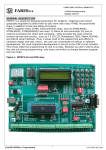
Em bin Te ch nologie s Pv t . Lt d.
ETM 1 3 1 Use r ’s m a n u a l
User’s Manual for
ETM 1 3 1
Em bin Te chnologie s Pvt . Lt d.
First Floor, Tri Murt i Towers, Plot No.34,
Gorai- I , Borivali ( W) , Mum bai - 400091, ( I ndia)
Telefax: 91- 22- 28685660
E- Mail: cust om er.support @em bin.com
ht t p: / / www.em bin.com
1
Em bin Te ch nologie s Pv t . Lt d.
ETM 1 3 1 Use r ’s m a n u a l
Cont e nt s
1 . I nt r oduct ion………………………………………………. .….…..……….3
1.1 Et hernet Connect ivit y………………………………………………………………5
1.2 Serial EEPROM………………………………………………………………………….6
2 . Ge t t ing St a r t e d… … … … … … … … … … … … … … … … … .… … … .… … … 7
2.1 ETM 1 3 1 I ncludes…………………………………………………………………….9
2.2 Power Supply Requirem ent s……………………………………………………9
2.3 Configuring t he syst em ……………………………………………………………9
3 . Boa r d D e scr ipt ion… … … … … … … … … … … … … … … … … … … … … … 9
4 . Conne ct or de t a ils a nd j um pe r se t t ings… … … … … … … … … … … 1 0
4.1 ETM131 board Layout ………………………………………………………….….11
4.2 Connect or & Jum per det ails of ETM131………………………………….11
4.2.1 Port connect or…………………………………………………………………..11
4.2.2 Power Socket …………………………………………………………….……...11
4.2.3 Et hernet Connect or……………………………………………………………11
4.2.3.1 Et hernet Connect or ( CN5) …………………………………….…11
4.2.4 Out put and I nput Connect ors…………………………………………..11
5
CD – Cont e nt s… … … … … … … … … … … … … … … … … … … … … … ..1 2
6
Run your Pr ogr a m s… … … … … … … … … … … … … … … .… … … … ..1 3
7
Applica t ions… … … … … … … … … … … … … … … … … … … … … … .… .1 5
7.1 Et hernet Module……………………………………………………………………...15
7.2 EEPROM…………………………………………………………………………………...16
2
Em bin Te ch nologie s Pv t . Lt d.
ETM 1 3 1 Use r ’s m a n u a l
1 . I nt r oduct ion
Em bin’s ETM 1 3 1 is a Serial t o Et hernet Convert er m odule wit h 8051. ETM 1 3 1 can
be used ext ensively t o read t he dat a over t he serial port and send t he dat a via
Et hernet
in
t he
packet s
form at .
At
t he
heart
of
t he
board
is
Phillips
P89C51RD2/ P89C668; t his provides advance feat ures like I SP. The m icro cont roller
has 64KB flash m em ory and 1KB/ 8KB on- chip RAM. The Module board com es wit h
RS- 232 int erface t o allow user t o program t he m icro cont roller direct ly from PC.
ETM 1 3 1 board reads t he dat a from any Serial Port and sends t o t he Et hernet ( LAN) .
ETM 1 3 1 is a unique hardware and soft ware com binat ion providing t he serial dat a
send t hrough t he Et hernet . Hardware reference and soft ware applicat ion program s
also sim plify 8051 based hardware and soft ware developm ent . This board is also
having t he facilit y of Soft ware flow cont rol or Hardware flow cont rol and No flow
cont rol, you can select t he Soft ware flow cont rol or Hardware flow cont rol or no flow
cont rol opt ion t hrough t he CONFI G m enu. SERI AL BUFFSI ZE is 100byt es, so wit hout
S/ W or H/ W flow cont rol we can t ransfer t he 100byt es at a t im e wit h out dat a loss.
The t im e gape bet ween t wo t ransm issions should be approxim at ely 5m sec. TCP
packet size is 140byt es. Before st at ing t he dat a t ransfer t he rem ot e syst em , which is
collect ing t he dat a, should be on, ot herwise t he dat a m ay loss. I n t he ETM131 no
feat ure of checking whet her rem ot e syst em is connect ed or not .
Pe r iphe r a ls:
•
Et hernet connect ivit y.
•
Serial EEPROM.
•
RS232 Serial I nt erface.
3
Em bin Te ch nologie s Pv t . Lt d.
1.1
ETM 1 3 1 Use r ’s m a n u a l
Et he r ne t ca r d conne ct ivit y: To connect t he Microcont roller t o t ransfer t he
dat a from Microcont roller t o t he Et hernet RTL8019AS is used in ETM 1 3 1 . Et hernet
connect ivit y is t he m ain feat ure of ETM 1 3 1 . So t hat one can use it according t o t he
need. RTL8019AS is connect ed t o t he Microcont roller t hrough t he port 0 and port 2.
I n ETM131 RTL8019 we have used in 8bit m ode in int errupt m ode. The fallowing are
t he feat ures of t he RTL8019 if user want s t o im plem ent his own developm ent he can
im plem ent on t his feat ures.
The RTL8019AS is a highly int egrat ed Et hernet Cont roller. Wit h t he t hree level
powers down cont rol feat ures, t he RTL8019AS is m ade t o be an ideal choice of t he
net work device for a GREEN PC syst em . The full- duplex funct ion enables
sim ult aneously t ransm ission and recept ion on t he t wist ed- pair link t o a full- duplex
Et hernet swit ching hub. This feat ure not only increases t he channel bandwidt h from
10 t o 20 Mbps but also avoids t he perform ance- degrading problem due t o t he
channel cont ent ion charact erist ics of t he Et hernet CSMA/ CD prot ocol. The Microsoft ’s
Plug and Play funct ion can relieve t he users from pains of t aking care t he adapt er’s
resource configurat ions such as I RQ, I / O, and m em ory address, et c. However, for
special applicat ions not t o be used as a Plug and Play com pat ible device, t he
RTL8019AS also support s t he j um per and propriet ary j um per less opt ions. To offer a
fully plug and play solut ion, t he RTL8019AS provides t he aut o- det ect capabilit y
bet ween t he int egrat ed 10BaseT t ransceiver, BNC and AUI int erface. Besides, t he
10BaseT t ransceiver can aut om at ically correct t he polarit y error on it s receiving pair.
Furt herm ore, 8 I RQ lines and 16 I / O base address opt ions are provided for grand
resource configurat ion flexibilit y. The RTL8019AS support s 16k, 32k & 64k byt e
BROM and flash m em ory int erface. I t also offers t he page m ode funct ion, which can
4
Em bin Te ch nologie s Pv t . Lt d.
ETM 1 3 1 Use r ’s m a n u a l
support up t o 4M- byt e BROM wit hin only 16k- byt e syst em m em ory space. Besides,
t he BROM disable com m and is provided t o release t he BROM m em ory space for ot her
syst em usage ( e.g. EMM386, et c.) aft er t he BROM program is loaded. The
RTL8019AS is built in wit h 16K- byt e SRAM in a single chip. I t is designed not only t o
provide m ore friendly funct ions but also t o save t he effort of SRAM sourcing and
invent ory.
Feat ures of RTL8019AS:
1. 100- pin PQFP
2. RTL8019 soft ware com pat ible
3. Support s PnP aut o det ect m ode ( RTL8019AS only)
4. Com pliant t o Et hernet I I and I EEE802.3 10Base5, 10Base2, 10BaseT
5. Soft ware com pat ible wit h NE2000 on bot h 8 and 16- bit slot s
6. Support s bot h j um per and j um per less m odes
7. Support s Microsoft ‘s Plug and Play configurat ion for j um per less m ode
8. Support s Full- Duplex Et hernet funct ion t o double channel bandwidt h
9. Support s t hree level power down m odes:
-
Sleep
-
Power down wit h int ernal clock running
-
Power down wit h int ernal clock halt ed
10. Built - in dat a prefet ch funct ion t o im prove perform ance
11. Support s UTP, AUI & BNC aut o- det ect ( RTL8019AS only)
12. Support s aut o polarit y correct ion for 10BaseT
13. Support 8 I RQ lines
14. Support s 16 I / O base address opt ions and ext ra I / O address fully decode
m ode ( RTL8019AS only)
15. Support s 16K, 32K, 64K and 16K- page m ode access t o BROM ( up t o 256
pages wit h 16K byt es/ page)
16. Support s BROM disable com m and t o release m em ory aft er rem ot e boot
5
Em bin Te ch nologie s Pv t . Lt d.
ETM 1 3 1 Use r ’s m a n u a l
17. Support s flash m em ory read/ writ e ( RTL8019AS only)
18. 16k byt e SRAM built in ( RTL8019AS only)
19. Use 9346 ( 64* 16- bit EEPROM) t o st ore resource configurat ions and I D
param et ers
20. Capable of program m ing blank 9346 on board for m anufact uring convenience
21. Support 4 diagnost ic LED pins wit h program m able out put s
1 .4 Se r ia l EEPROM :
The AT24C512 provides 524,288 bit s of serial elect rically
erasable and program m able read only m em ory ( EEPROM) organized as 65,536 words
of 8 bit s each. I n ETM 1 3 1 AT24C512 is connect ed t o serially t o Microcont roller at
P1.6 and P1.7 ( I 2C bus for P89C668) . This peripheral can be used in m any indust rial
and com m ercial applicat ions where low power and low volt age operat ion is essent ial.
Feat ures of AT24C512:
1. Low- volt age and St andard- volt age Operat ion
–
2.7 ( VCC = 2.7V t o 5.5V)
–
1.8 ( VCC = 1.8V t o 3.6V)
2. I nt ernally Organized 65,536 x 8
3. 2- wire Serial I nt erface
4. Schm it t Triggers, Filt ered I nput s for Noise Suppression
5. Bi- direct ional Dat a Transfer Prot ocol
6. 1 MHz ( 5V) , 400 kHz ( 2.7V) and 100 kHz ( 1.8V) Com pat ibilit y
7. Writ e Prot ect Pin for Hardware and Soft ware Dat a Prot ect ion
8. 128- byt e Page Writ e Mode ( Part ial Page Writ es Allowed)
9. Self- t im ed Writ e Cycle ( 5 m s Max)
10. High Reliabilit y
–
Endurance: 100,000 Writ e Cycles
–
Dat a Ret ent ion: 40 Years
6
Em bin Te ch nologie s Pv t . Lt d.
ETM 1 3 1 Use r ’s m a n u a l
2 . Ge t t ing St a r t e d
2 .1 ETM 1 3 1 I nclude s:
ETM 1 3 1 Package cont ent s are:
ETM 1 3 1 Board.
Serial Cross Cable.
Power Adapt or.
Syst em CD- ROM wit h Applicat ion program s.
2 .2 Pow e r Supply Re quir e m e nt s:
ETM 1 3 1 Board is provided wit h + 9Volt s out put adapt or wit h 230V AC input . The
board has a + 5Volt s Regulat or on- board, which provides supply t o t he ent ire device
on t he board.
2 .3 Configur ing t he syst e m :
Connect t he Serial cable provided t o t he DB9 connect or on ETM 1 3 1 board &
COM1/ COM2 of t he Com put er. Plug in t he Power adapt or in 230VAC m ains socket &
connect t he + 9V pin of power adapt or t o t he ETM 1 3 1 board ( CN1) t he board is now
ready t o be swit ched on.
As soon as t he reset swit ch S1 is pressed configurat ion m ode is shown on t he hyper
t erm inal as “ Please Ent er for Configurat ion” . At t his point press “ ENTER” key quickly
t o configure t he syst em . Please follow according t o t he m enu shown .
7
Em bin Te ch nologie s Pv t . Lt d.
ETM 1 3 1 Use r ’s m a n u a l
3 . Boa r d D e scr ipt ion
Philips 8- bit , 80C51- com pat ible P8xC51RD2 Microcont roller ( DI P- 40/ PLCC- 44,
12 MHz clock frequency)
On- chip FLASH.
64KB on- chip FLASH wit h download ut ilit y for in- Syst em
( I SP) FLASH
Program m ing. 1KB of on- chip RAM.
512KB ext ernal serial I 2C- EEPROM.
RS232 serial int erface
Et hernet Connect or RJ45.
Single 5V power supply.
4 . Conne ct or de t a ils a nd j um pe r se t t ings
The ETM 1 3 1 board is available wit h Serial Connect or and RJ45 for Et hernet dat a
t ransfer t hrough t he m icrocont roller. Below Sect ions give t he Board layout & Board
Jum per Det ails.
8
Em bin Te ch nologie s Pv t . Lt d.
ETM 1 3 1 Use r ’s m a n u a l
4 .1 ETM 1 3 1 boa r d La yout :
4 .2 Conne ct or & Jum pe r de t a ils of ETM 1 3 1 :
4 .2 .1 Por t conne ct or :
PORT0 :
CN3 Pin2 To 9 – P0.0 To P0.7
PORT1 M a x - 2 3 2 :
P1.0 To Max pin9
P1.1 To Max pin10
PORT2 CN 4 :
CN4
CN4
CN4
CN4
CN4
CN4
CN4
CN4
CN4
Pin3
Pin4
Pin5
Pin7
Pin8
Pin9
Pin10
Pin11
Pin6
-
P2.5
P2.7
P2.6
P2.0
P2.1
P2.2
P2.3
P2.4
P3.2
CN 2 To M AX2 3 2 :
9
Em bin Te ch nologie s Pv t . Lt d.
ETM 1 3 1 Use r ’s m a n u a l
CN2 – Pin2 To Pin13
CN2 – Pin3 To Pin14
CN2 - pin5 To Ground
CN2 - pin7 To Pin7
CN2 - pin8 To Pin8
CN 1 pow e r supply
Jum pe r Jp2
Pin 1- Pin 2 Closed: - Non I nvert ed I nt errupt Signal
Pin 3- Pin 4 Closed: - I nvert ed I nt errupt Signal ( default )
J1 is for com pa ny use
CN3 of base board to CN1 of upper board
CN4 of base board to CN2 of upper board
Upper board Layout :
10
Em bin Te ch nologie s Pv t . Lt d.
ETM 1 3 1 Use r ’s m a n u a l
RJ4 5 ( CN 5 ) To 8 0 1 9 :
P1
P2
P3
P4
P6
P7
To
To
To
To
To
To
Pin45
Pin46
Pin59
Ground
Pin58
Ground
CN 1 t o ba se boa r d CN 3
CN1-1 NC
CN1-2 SD0 Data Bus
CN1-3 SD1 Data Bus
CN1-4 SD2 Data Bus
CN1-5 SD3 Data Bus
CN1-6 SD4 Data Bus
CN1-7 SD5 Data Bus
CN1-8 SD6 Data Bus
CN1-9 SD7 Data Bus
CN 2 t o ba se boa r d CN 4
CN2-1 Vcc
CN2-2 SD0 Address Bus
CN2-3 SD1 Address Bus
CN2-4 SD2 Address Bus
CN2-5 SD3 Address Bus
CN2-6 SD4 P3.2
CN2-7 SD5 Address Bus
CN2-8 SD6 Address Bus
CN2-9 SD7 Address Bus
CN2-10 SD8 Address Bus
CN2-11 SD9 Address Bus
CN2-12 SD2 NC
11
Em bin Te ch nologie s Pv t . Lt d.
ETM 1 3 1 Use r ’s m a n u a l
5 . CD - Cont e nt s
WI NI SP soft ware
KEI L Com piler ( Evaluat ion version, 2K code size)
Sam ple C codes for Serial t o Et hernet conversion, I 2C EEPROM.
12
Em bin Te ch nologie s Pv t . Lt d.
ETM 1 3 1 Use r ’s m a n u a l
6 . Run your Pr ogr a m s
The ETM 1 3 1 m ain m icro cont roller is 89V51RD2, which has on- chip 64k of flash 1k
Ram . The CD provided has t he I n- Syst em - Program m ing soft ware WI NI SP t hat is t o
be inst alled in your com put er. To inst all t he WI NI SP soft ware run t he set up provided
in t he CD. Soft ware flow cont rol ( Xon/ Xoff) is required for com m unicat ion. Or t he
dat a should be wit hin t he m axim um buffer size. To Program ( download) t he hex file
in t he flash follow t he below sim ple st eps:
D ow nloa d st e ps
Connect t he Power adapt or t o t he board ( do not swit ch on) .
Connect t he supplied serial cable t o t he board and t he COM1/ COM2 of
com put er
Press t he program m ing swit ch ( S1) so t hat it rem ains in down
posit ion.
Power on t he Board ( swit ch t he m ains supply) .
The green led on board should light up indicat ing proper power supply.
The red led should also light up indicat ing program m ode.
Run t he WI NI SP soft ware.
Under t he param et ers heading select t he following
CHI P – 89V51RD2
PORT – COM1/ COM2
OSC ( Mhz) – 12
Using t he LOAD ( Alt - L) but t on load t he appropriat e HEX File or hello.
Hex file provided in CD.
Click t he ERASE BLOCK ( Alt - E) but t on; select t he flash m em ory block
t o be erased. Click t he ERASE! But t on, t he select ed block will flash
13
Em bin Te ch nologie s Pv t . Lt d.
ETM 1 3 1 Use r ’s m a n u a l
wit h Pink color. Once com plet ed t he Block Erase Select ion window will
close.
Press t he PROGRAM PART ( Alt - P) but t on; wait t ill t he St at us Display
shows “Program m ing Flash Successful” is displayed.
Now close t he WI NI SP soft ware & swit ch off t he m ains.
Press t he
program m ing swit ch ( S1) again so it com es in up posit ion.
Open t he hyper t erm inal if hello. Hex file is loaded & select t he baud
rat e t o 9600, Set Dat a Bit s= 8, parit y bit = None, Echo= Off.
Swit ch on t he Board power, which will run hello. Hex file displaying t he
st ring ”Press Ent er for configurat ion” in t he hyper Term inal
14
Em bin Te ch nologie s Pv t . Lt d.
7.
ETM 1 3 1 Use r ’s m a n u a l
Applica t ions
ETM 1 3 1 can be used t o send Serial dat a t o Et hernet and t o Explore t he
8051 core & as a Test Plat form t o download t he program s t o 89V51RD2
flash t o run t he Program , check t he desired out put & if required change
t he program & download it t o t he m icrocont roller flash wit hout rem oving it
from t he board.
The Sam ple C code provided
wit h
t he ETM 1 3 1
m odule are self
explanat ory wit h com m ent s t hat help you underst and t he Et hernet
m odule.
7.1 ETM 1 3 1 . Download t he .hex file of sim ple keyboard program and open hyper
t erm inal. Configure it for t he baud rat e of 9600 and aft er pressing t he key
different m essages are displayed as coded in source code. Aft er recognizing
t he key pressed in m ain rout ine passes only t he value of t he key and t he
rout ine t akes t he act ion wit h respect t o t he key value. So for furt her changes
t o m ake it m ore useful t he developers have t o do few changes in “get key ( ) ”
as per applicat ion.
a) Launch t he Hyper t erm inal program .
b) Under " Bit s per second" , choose " 9600 "
c) Under " Dat a bit s" , choose " 8 "
d) Under " Parit y" , choose " None "
e) Under " St op Bit s" , choose " 1 "
f)
Under " Flow Cont rol" , choose " Soft ware flow cont rol/
Xon- Xoff " or Hardware flow cont rol/ CTS- RTS.
15
Em bin Te ch nologie s Pv t . Lt d.
ETM 1 3 1 Use r ’s m a n u a l
g) Flow cont rol: Xon/ Xoff or ( None if dat a size is wit hin
t he m axim um buffer size)
7.2 EEPROM : Source code for t he EEPROM dem onst rat es how t o st ore t he Dat a
in EEPROM by suing I 2C prot ocol. By using t his sam ple code dat a can be
st ored and ret rieved from EEPROM.
16