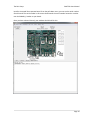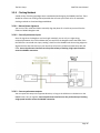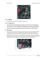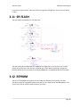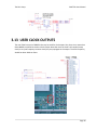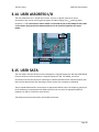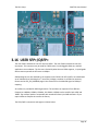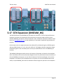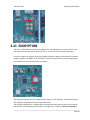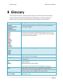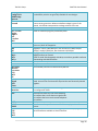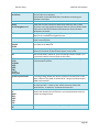
1
Logic Emulation
ASIC Verification
Algorithm Acceleration
User Manual
DNV7F2A
DNV7F2A
User Manual
The Dini Group
DNV7F2A User Manual
Contents
1
INTRODUCTION ............................................................................................................................................. 5
1.1
1.2
1.3
2
QUICK START GUIDE ...................................................................................................................................... 8
2.1
3
STEPS TO FOLLOW .............................................................................................................................................8
HARDWARE ................................................................................................................................................. 17
3.1
3.2
3.3
3.4
3.5
3.6
3.7
3.8
3.9
3.10
3.11
3.12
3.13
3.14
3.15
3.16
3.17
3.18
3.19
3.20
3.21
3.22
3.23
3.24
3.25
3.26
3.27
3.28
3.29
4
AUDIENCE........................................................................................................................................................5
CONVENTIONS ..................................................................................................................................................5
RESOURCES ......................................................................................................................................................5
OVERVIEW .....................................................................................................................................................17
VIRTEX 7 FPGA ..............................................................................................................................................18
CLOCK RESOURCES ..........................................................................................................................................19
NMB BUS .....................................................................................................................................................22
DAUGHTER CARD CONNECTORS .........................................................................................................................24
FPGA CONFIGURATION ..............................................................................................................................28
MARVELL CPU ...............................................................................................................................................29
CONFIG FPGA................................................................................................................................................35
RS232 .........................................................................................................................................................36
USER LEDS ..................................................................................................................................................37
SPI FLASH ....................................................................................................................................................38
EEPROM .....................................................................................................................................................38
USER CLOCK OUTPUTS................................................................................................................................39
USER ASSORTED I/O ...................................................................................................................................40
USER SATA ..................................................................................................................................................40
USER SFP+/QSFP+ .......................................................................................................................................41
GTX EXPANSION (DNSEAM_NS) .....................................................................................................................42
USER PCI EXPRESS .......................................................................................................................................43
USER USB 3.0 ..............................................................................................................................................44
USER FPGA B GTX SMAS ..............................................................................................................................45
ENCRYPTION ...............................................................................................................................................46
JTAG ...........................................................................................................................................................47
MECHANICAL ..............................................................................................................................................47
POWER .......................................................................................................................................................49
HEAT ...........................................................................................................................................................49
RESET ..........................................................................................................................................................50
XADC...........................................................................................................................................................52
LED REFERENCE LIST ...................................................................................................................................53
TEST POINT REFERENCE LIST.......................................................................................................................55
SOFTWARE .................................................................................................................................................. 59
4.1
4.2
EMU HOST SOFTWARE ......................................................................................................................................59
WRITING YOUR OWN SOFTWARE ........................................................................................................................64
Page 3
The Dini Group
4.3
4.4
4.5
5
GENERAL PROCEDURE ......................................................................................................................................76
ORDERING INFORMATION ........................................................................................................................... 77
7.1
7.2
7.3
7.4
8
NMB SPACE MAP...........................................................................................................................................74
COMPILING ....................................................................................................................................................75
TROUBLESHOOTING .................................................................................................................................... 76
6.1
7
HOW EMULIB WORKS ......................................................................................................................................65
MARVEL ENVIRONMENT ...................................................................................................................................66
MORE INFORMATION.......................................................................................................................................73
REFERENCE DESIGN ..................................................................................................................................... 74
5.1
5.2
6
DNV7F2A User Manual
PART NUMBER ...............................................................................................................................................77
HOW TO ORDER .............................................................................................................................................77
BOARD OPTIONS .............................................................................................................................................77
COMPLIANCE INFORMATION..............................................................................................................................77
GLOSSARY ................................................................................................................................................... 78
Page 4
The Dini Group
DNV7F2A User Manual
1 INTRODUCTION
Welcome to the DNV7F2A FPGA-based ASIC Prototyping Platform. This manual will assist in setting
up, using, and understanding the hardware aspects of this product.
1.1 Audience
This product is marketed and sold to engineers who are familiar with circuit board design,
physically probing AC waveforms, programming FPGAs, wiring HDL code, reading device data
sheets, reading C source code, and writing software. The provided support material all assumes
that the user already has these skills.
1.2 Conventions
Computer input or output
1.3 Resources
The following list includes the resources that you are expected to make use of.
1.3.1
Website
The product page for this product is on the internet, here:
http://www.dinigroup.com/DNV7F2A.html
This page contains:
- Block Diagram of the board
- Marketing Product description
- List of supported features
- Latest Errata
- Latest software and firmware update package
- Latest version of this document.
1.3.2
Product Package
The board comes with a USB memory stick with files on it. On the root directory, there is a file
called "Support Package Contents.pdf" that describes the contents and the directory structure.
Page 5
The Dini Group
DNV7F2A User Manual
This package contains the software installed on the board as well as the software that should be
installed on your host computer.
1.3.3
Reference Design
The product package contains a set of FPGA designs written in Verilog HDL that produce working
configuration files for the FPGAs on the DNV7F2A. Project files and batch script files that use Xilinx
Vivado to build the designs are also provided. These example files can be used to quickly create
working .bit files for the FPGAs.
The reference design implements every feature on the board, including DDR3 memory, Rocket I/O,
and others. You are free to adopt any of the device controllers used in this reference design.
For most customers, the most interesting part of the reference design will probably be the UCF file,
which contains a list of all the usable signals connected to the FPGA and the correct IOSTANDARD
attribute to use with each.
1.3.4
Schematics and Netlist
This user manual does not list specifications for all of the devices connected to the FPGAs, and so to
correctly use them, you will have to refer to the device datasheet and the schematic. The schematic
is provided in PDF format. If you need a machine-readable format, you can use the provided ASCII
netlist of the board. The ASCII netlist contains only nets on the DNV7F2A that are connected to
usable I/O on the FPGA.
1.3.5
Other Relevant Documentation
The principal form of control and communication with the DNV7F2A system is via the Emu software
tools. This manual will discuss the use of Emu in performing basic operations on the board, such as
FPGA configuration, clock setting, and data transfer. For a more detailed overview of the Emu
software, please see the Emu manual at this URL:
http://www.dinigroup.com/product/data/DNV7F2A/files/Emu_Manual.pdf
Two of the primary board interfaces, the DINAR1 general-purpose I/O interface, and the
DNSEAM_NS high-speed serial breakout, are proprietary to Dini Group. These are intended to be
used for I/O breakout from the DNV7F2A main board. This manual will describe the interfaces and
their connection to the user FPGA on the DNV7F2A. To obtain a better understanding of the
interfaces, especially if you want to design a custom daughter board, please see the relevant
specifications on the product CD: /Daughtercards/Specifications.
1.3.6
Device Datasheet Library
There is a PDF datasheet provided for every part used on the board. It is in the user support
package, see /Documentation/Datasheets.
Page 6
The Dini Group
1.3.7
DNV7F2A User Manual
Xilinx
Questions about the use of Virtex 7 FPGAs or Vivado that aren't specific to the DNV7F2A should be
directed to Xilinx.
1.3.8
EMAIL AND Telephone Technical support
Email [email protected] for the best and quickest connection to an actual Engineer that will
be able to directly answer your questions.
Phone support is also available Pacific Standard Time from 9AM to 5PM from Monday through
Friday, excluding USA federal holidays. Support is available in English. Support for boards purchased
through distributors can additionally be provided by the distributor. Distributors are listed in the
ordering information section.
Telephone (USA): 858-454-3419
Page 7
The Dini Group
DNV7F2A User Manual
2 Quick Start Guide
This section will walk through an example session using the board.
2.1 Steps to Follow
2.1.1
Examine Contents of Box
The box containing the product should have come with the following units:
DNV7F2A board (green -> revision 1)
RS232 serial Cable
DB9-to-IDC cable adapter
USB Stick containing user support package
USB Stick containing FPGA .bit files and a shell script.
Packing foam
Page 8
The Dini Group
DNV7F2A User Manual
ATX Power supply
PCI Express cable
PCI Express host adapter card
2.1.2
Before you power on
Take ESD precautions whenever handling the board.
Place the board on a clear desk with static control padding. You can use the silver-colored bag the
board comes wrapped in as a static control surface. Make sure you neutralize the static in your
fingers with the surface before every time you contact the board.
2.1.3
Connect a system to host PC interface
Configuration FPGA PCIe
MV78200 USB (media)
MV78200 USB (to Host)
MV78200 LAN
EthernetPCIe
MV78200 PCIe
At least one host PC-facing interface should be connected to allow the user to interact with the
DNV7F2A. These interfaces are described in this section.
2.1.3.1 Install the PCI Express adapter board in a PCI Express slot (optional)
During the course of your project, if you intend to control the board using PCI Express, then you
should complete this step.
Page 9
The Dini Group
DNV7F2A User Manual
The board fits into any 8x or 16x PCI Express slot. Make sure the computer is powered off when you
install the board into it. There are two x4 cable connectors on the board. You should use only the
bottom one with the DNV7F2A because the DNV7F2A PCI Express interfaces only support 1x or 4x
PCI Express links. The top connector on the PCI Express cable adapter card is for use with 8x links.
Connect one end of the provided PCI Express cable to the bottom connector of the adapter card,
and the other end of the cable to the DNV7F2A. The correct connector is labeled “MARVELL PCIE”
for use with the Emu software. For general-purpose applications, use this connection. If you require
higher throughput and lower latency on the link, you may connect the PCIe cable to the “CFPGA
PCIe” port and use the PCIEDIRECT interface through Emu. See the Emu manual for details on
selecting the interface from the host software.
2.1.3.2 Connect Ethernet Cable
This step is optional. During the course of your project, if you intend to use Ethernet to control the
board, then you should complete this section.
Have a computer network. In order to be able to access the board over the network, the network
must support DHCP. Otherwise, the board will fail to have a usable IP address. Connect the RJ45
connector on the DNV7F2A to your network. If DHCP is not available a static IP address can be
assigned to the board. See the Emu User Manual for more information. Traffic must be allowed on
certain ports in order for the Emu Software to communicate with the board. See the Emu User
Manual for more information.
2.1.3.3 Connect USB Cable
This step is optional. During the course of your project, if you intend to control the board directly
from a computer over USB, then you should complete this step.
Page 10
The Dini Group
DNV7F2A User Manual
Connect a USB cable from the host computer to the "USB type B" connector on the board. If the
board is plugged into PCI Express, the computer that connects to the board with USB does not
necessarily need to be the same computer.
2.1.3.4 Connect MV78200 RS232
The MV78200 processor may be accessed via RS232. If you are using the board without a chassis
interface with the header circled above, otherwise use the top header on the front of the chassis.
The RS232 port provides a root shell within the Linux environment running on the CPU; this may be
used (via DiniCMOS) to configure FPGAs, set clocks, etc. See the DiniCMOS documentation (part of
the Emu manual) for more details. In general, this interface is not recommended; for new users, it
is recommended to use of the Emu-compatible interfaces listed earlier in this section.
2.1.3.5 Connect FPGA JTAG
This is just a JTAG connection to the user FPGA. See section 3.22. This is if you want to configure the
FPGA directly and talk to it over JTAG, f.ex. for debugging with Chipscope.
2.1.4
Connect power cables
The DNV7F2A requires an ATX power header, an EPS (4 pin CPU power), and a PCIe Graphics power
cable to be attached, to power the board. These should all come from the same power supply. It is
recommended that the power supply use a single rail for these connections. If your power supply
does not feature a single +12V rail, do not connect the PCIe graphics power header. No
performance degradation will be experienced in this configuration.
Page 11
The Dini Group
2.1.5
DNV7F2A User Manual
Power on the board
If you are using the board in a chassis, simply flip the switch on the front panel. Otherwise, install a
jumper in header J23 positions 9-10 (pictured below), and then turn on the power supply.
The board has a self-boot process that takes 30 to 45 seconds.
2.1.6
Using a USB pen drive to control the board
The board is provided with a USB pen drive that has on it a Linux shell script (startup.sh). If you plug
the USB stick into the board, then the board will automatically run the shell script. The shell script
on the provided pen drive will cause the FPGAs to load with the reference design .bit files. You can
tell that the .bit files are loading because after each FPGA configures, a blue LED will appear on the
board. A USB pen drive left connected to the board will execute each time the board is powered on,
allowing the user to customize clock settings, FPGA load files, and other features, without the need
for host control or software intervention.
2.1.7
Host Software
Whether the board is connected to a computer using USB, MV78200 PCI Express or Ethernet, the
board is controlled using a program that Dini Group has provided called "Emu". The Emu program is
provided in source and as binaries on the user support package. See the Emu User Manual for
additional information on installing and using the Emu software.
The rest of this guide will assume you are using a Windows computer; however you can also use
Linux. If you are using Linux the instructions may be slightly different, although the Emu program is
cross-platform and should operate in the same way irrespective of the host PC OS.
Page 12
The Dini Group
DNV7F2A User Manual
If you are using PCI Express then you need to install a PCI Express driver. This can be done in
Windows using the "device manager". The driver files are provided in the support package
/Host_Software/emu/Drivers/windows_pci. Windows should detect the Dini Group board when it
is attached to the system, and prompt you to help it locate a driver; just have it find a driver in this
location.
If you are using USB then you will need to install a USB driver. [Linux does not require a USB driver].
This can be done in Windows using the "device manager". The driver files are provided in the
support package
/Host_Software/emu/Drivers/windows_usb.
Ethernet does not require a driver.
2.1.8
Selecting a board
Run the provided "emu" program, located in the user support package here:
/Host_Software/emu/App/out_release/emu_gui_win32.exe
This window will appear.
From the "Board" menu, choose "select board". If you are connected to the board over PCI Express,
USB and Ethernet simultaneously, then there will be three options in the pull-down menu. Each
Page 13
The Dini Group
DNV7F2A User Manual
interface is treated like a separate board. From the pull-down menu, you can see the serial number
of each board. The serial number in this menu should match the serial number located on a sticker
near the DINAR1_1 header on your board.
Once you have selected a board, your window should look like this.
Page 14
The Dini Group
2.1.9
DNV7F2A User Manual
Configure an FPGA
You can configure an FPGA by clicking on the image of it in EMU and selecting "configure" from the
pop-up window. There are some example .bit files that you can use in the support package located
at
/FPGA_reference_designs/Programming Files/dn0267_dnv7f2a/user_fpga/MAINTEST
Be sure to choose bit files that are compiled for the correct type of FPGA that you have installed on
the board, as indicated by the folders they are stored in. For example for a XC7V2000T part, make
sure to select from the “V2000T” sub-directory of MAINTEST.
After the FPGA successfully configures, a blue dot will appear next to any configured FPGA.
2.1.10 Setting board controls and options
The primary board settings that you will need to modify are the clock settings. There are three
clocks on the board that have modifiable options. Let's change the clock frequency of G0 just for
kicks.
In the EMU window, click on the right side where it says "CLOCKS: G0". A pop-up menu will allow
you to change the frequency of clock G0. You can also change the frequency using the
"Clocks/Temps" menu in the menu bar. The clock frequency of the five main clocks are periodically
measured and displayed on the screen.
Page 15
The Dini Group
DNV7F2A User Manual
2.1.11 Hardware Verification Test
To run the hardware test, from the "Test" menu, select "selected tests".
The tests that you can run now are any of the tests under “FIELD TESTS”. Let's skip the "FACTORY
TESTS" for now. After you hit the "OK" button, the program will ask you to locate the "bit file
directory". This is where the test FPGA load files are stored. Select this folder in the user support
package:
/FPGA_Reference_designs/Programming Files
After each test runs, the Emu window will print "PASS" or "FAIL", and at the end of testing a
summary will be presented with the results of each test that was run.
Note that the factory tests require specialized hardware and therefore cannot be run in the field. If
these conditions are not met then the test will fail.
Page 16
The Dini Group
DNV7F2A User Manual
3 Hardware
This section describes the board hardware.
3.1 Overview
Below is a block diagram of the board.
The board contains two Xilinx Virtex-7 FPGAs in the “FF1761” package. There are 2 different Xilinx
part numbers that come in this package, VX690T, and V2000T. All 2 of these are compatible with
this board (in any speed grade) although the 10Gbps interfaces can only be used with -2 speed
grades and faster.
The Virtex 6 "ConfigFPGA" is not intended for your use, so you should think of it as more of a
"controller/bus switch/monitor".
Page 17
The Dini Group
DNV7F2A User Manual
To connect to other systems, or off-board I/O, there are three "daughtercard" connectors provided.
In the block diagram these appear as yellow rectangles. The user is expected to buy a daughter card
that contains the I/O interface that is required, or to design their own.
Getting data on and off the board is accomplished through the Marvell CPU. It provides USB,
Ethernet, PCI Express, interfaces. It connected to the user FPGAs through the "NMB" interface,
which provides an easy-to-use 20-30MB link to the user FPGA. A high-speed PCI Express only NMB
solution is also available if greater bandwidth is required; up to 380MB/s. Contact Dini Group
support for more information. The standard NMB interface inside the FPGA and on the host PC is
very simple, because all of the software and hardware between has already been designed, proven,
and optimized.
3.2 Virtex 7 FPGA
The Virtex 7 FPGA provides the latest features, largest sizes, and fastest speeds from Xilinx.
3.2.1
Stuffing Options
Below there is a table that describes the major differences between the available FPGAs. Only
FPGAs that Xilinx sells in the "1761" (FF, FFG, FH, FHG) packages are compatible with this board.
FPGA
VX690T
V2000T
Speed
Grades
1, 2, 3
1, 2
Flip-flops
866,400
2,443,200
Equivalent
ASIC Gates
4.99M
3.4M
All Board
Features?
Y
Y
25x18
multipliers
3,600
2,160
Memory
(bits)
52.9M
46.5M
Each V2000T FPGA can emulate approximately 14.1 million ASIC gates reasonably; however this is
only an estimate. It is strongly recommended that you synthesize your actual ASIC design, mapping
to FPGA technology to get an accurate FPGA utilization estimate.
3.2.2
Speed Grades
Xilinx FPGAs usually come in three speed grades. There is no rule of thumb to estimate which speed
grade you will need to run your design at your target frequency. You will only know this once you
have run a synthesis, with FPGA place-and-route, targeting the actual FPGA device that you will be
using.
The transceivers are limited to 6.6Gbps for the -1 speed grades, 10.3125Gbps for the -2 speed
grades, and 12.5Gbps for the -3 speed grades. Verify your transceiver performance requirements
before selecting your FPGA. Notably, to run 10Gbps Ethernet and PCIe GEN3, -2 speed grade or
faster parts must be used.
Page 18
The Dini Group
3.2.3
DNV7F2A User Manual
Upgrades
If you would like to install smaller/slower FPGAs when you order the board, and later upgrade
FPGAs to larger parts, this is possible; however you should request this before ordering the board
because there are risks involved in attempting to add FPGAs to an existing board. Costs associated
with the upgrade should be negotiated with Dini Group sales.
3.2.4
Safe Handling of FPGAs
There are three easy ways to break the FPGAs.
1) Static electricity
Make sure you keep the board on a static controlled surface, and that you neutralize your body
with that surface before handling the board. Especially sensitive are the FPGA I/Os. These are
exposed on the daughter card headers and other connectors.
2) High Voltage
The FPGA I/O can only withstand voltages between GND and the VCCO power supply. When
interfacing the board to some external I/O, make sure your I/O signals are driven at levels that do
not exceed VCCO. If you do not know what VCCO is, then you probably should not be interfacing
the board to some external I/O. Note that the maximum allowable VCCO on Virtex 7 is 1.8V. If you
are interfacing with a 3.3V device, then you will need voltage translators.
3) Board warp
If the board undergoes mechanical stress, the FPGA pins (balls) can separate from the PCB and
result in non-connected signals. The most common mechanical stress occurs when installing and
removing connectors. Make sure that when installing a connector, you are supporting the
connector from the opposite side, so that board warp does not absorb the force of the insertion.
The board baseplate and stiffeners should be left installed to help reduce flex on the V7F2A system.
3.3 Clock Resources
The board provides many clocking resources for general use. The sources and speeds of these
clocks are designed to be as flexible as possible to accommodate a wide range of applications.
3.3.1
Clock pins on the FPGA
Xilinx Virtex-7 parts have removed the notion of “global clock” pins. The two types of clock-capable
I/O on the part (excluding the GTX transceiver reference clocks) are MRCC and SRCC pins. The
difference between the pins mostly applies to phase-sensitive applications (such as clocking a
source-synchronous interface) or applications demanding the use of higher-performance regional
buffers (BUFMR or BUFR) rather than global clock resource (BUFG).
Page 19
The Dini Group
DNV7F2A User Manual
Either MRCC or SRCC pins may be used to route to a BUFG or to a clock management tile (CMT).
Either type of pin may be used to clock regional clock resources (i.e. a bank) associated with the
bank into which the clock is connected. MRCC pins have the ability to clock as many as three clock
regions using BUFMRs; this Is useful when designing fast, wide, source-synchronous interfaces (i.e.
a DDR3 SODIMM interface or similar).
The DNV7F2A’s user FPGA is pinned out to maximize the amount of clocking resources available to
the user and ensure flexibility across all board-level interfaces. For more details on how to clock a
particular interface, please see the relevant section further on in this chapter.
Any clock signal going into the FPGA must be terminated to function correctly. This includes all inboard clock resources. For differential clocks, it is usually sufficient to enable the DIFF_TERM
attribute on the IBUFDS element used for the clock input. Make sure you enable DIFF_TERM for
all of the relevant clocks in your design!
3.3.2
Global Networks
The global clocks are high accuracy, low jitter programmable synthesizers connected to user FPGA
MRCC pins. There is no set function for these clock networks. They may be used to clock logic or
any on-board interface, although in general dedicated clock sources are provided for all high-speed
interfaces.
3.3.3
Clocks G0, G1, G2, G3, G4
The clocks G0, G1, G2, G3, and G4 are from a synthesizer that can produce any frequency from
2KHz to 700MHz with a 50ppm tolerance or better. They also have the option of being used with
either a differential or single-ended off-board signal generator.
Page 20
The Dini Group
DNV7F2A User Manual
The synthesizer used is a high-performance, low jitter, high-precision clock generator chip, the
Si5326. To change the clock frequency you can use the EMU software.
The clocks G0, G1, G2, G3, and G4 can also be set to distribute a signal from an external source.
Note that the Si5326 cannot accept input frequencies lower than 2kHz. For very low input
frequencies you may consider using the user FPGA SMA inputs described in section 3.3.4.
3.3.4
User FPGA SMA inputs
There is a single pair of AC-coupled SMAs connected to an MRCC clock input pair on each user
FPGA.
There is no defined purpose for this input. Given that it is on an MRCC pair it is possible that it
would be useful for sending a clock into the user FPGA.
Page 21
The Dini Group
3.3.5
DNV7F2A User Manual
GTX Transceiver Reference Clocks
All of the GTX interfaces have some form of REFCLK allocated for them by the DNV7F21A. Usually
this consists of either a selectable-frequency oscillator (the choices are usually relevant for the
interface bit rate) or an externally-provided clock source, f.ex. for the PCIe downstream interface.
The REFCLK implementations are interface-specific and are described in the relevant sections of this
chapter.
3.3.6
From the DINAR1 Interfaces
The DINAR1 interface designates pairs for clocking the interface. Please see the section that
describes the DINAR1 interfaces.
3.3.7
NMB
The NMB interface includes one clock signal running at 50 or 100MHz. This clock is free-running,
and is not configurable. It is received by the FPGA from the configuration FPGA.
3.3.8
Generating clocks from FPGAs
Clocks may be generated in an FPGA using a CMT, PLL, or other logic. That means you can do all of
your frequency generation in the FPGA, if so desired.
3.4 NMB Bus
The NMB bus is the primary means you will use to get high quantities of data on and off the board.
If you want to use the provided software (EMU) to push data to the board over USB, Ethernet and
PCI Express, then you are required to interface to NMB in your FPGA design.
3.4.1
Protocol
You are expected to know nothing about the protocol of NMB and only interface to it using the
provided HDL interface wrapper in your FPGA on one end, and in the EMU C++ code on the other
end. This short section describes the implementation of the interface. I recommend you skip this
"protocol" section. It is useless to know anything here.
The NMB interface is a physically point-to-point connection from each FPGA to the configuration
FPGA. The point-to-point connection consists of 40 signal wires, which are used as 20 LVDS pairs.
These pairs are further divided into 10 signals in each direction, with 1 clock signals, 1 control signal
and 8 data signals. The clock frequency of the interface is 1GHz (500 MHz clock with DDR capture).
The theoretical throughput is therefore 1GB/sec in both directions simultaneously.
The protocol supports four channels, demand mode, bursts, interrupts, link detection, some FIFO
flags, and more. The data to/from the FPGA is stored in buffers in the DRAM of the Marvell
processor.
Page 22
The Dini Group
3.4.2
DNV7F2A User Manual
User Interface
An HDL module is provided in the support package here:
/FPGA_Rererence_designs/common/NMB/nmb_user_interface.v
See Documentation/Manual/Dini Buses User FPGA Design Manual.pdf and
Documentation/Manual/PCIe DMA (ConfigFPGA design) User Manual.pdf for details on
implementing the NMB FPGA module. More or less the nmb_user_interface.v provides a simple
Address/DataIn/DataOut type interface. You should think of the interface as a memory space.
On the C++ side of the NMB there are simple functions like
emu_nmb_read(address, buffer, size)
that can be used to view this memory space. The code for this is found in the support package here
/Host_Software/emu/App/out_release/[release]/Software/emu/App/source/EMULIB/diniboard.h
See Documentation/Manual/Emu_Manual.pdf for details on the Host side of NMB communication.
3.4.3
Memory Spaces
For additional information, read the Emu Manual sections on NMB:
/Documentation/Manual/Emu_Manual.pdf
The memory space is 64-bit. Each address represents a single byte (NMB uses “byte addressing”),
however the data is required to be read and written in blocks of 32-bits. Addresses supplied to the
interface must be divisible by 4. Therefore, the bottom 2 bits of the address space are unused and
always zero.
Additionally, since there are no chip-selects on the NMB bus, it is necessary to pre-allocate address
ranges for devices on the bus. On this board, there is only one device; the NMB address ranges that
it responds to on the bus are given here:
Target
FPGA A
FPGA B
3.4.4
Starting Address
0x00000000_00000000
0x01000000_00000000
End Address
0x00FFFFFF_FFFFFFFC
0x01FFFFFF_FFFFFFFC
Error Conditions
Occasionally error conditions may occur and the interface may return error codes. There is no
defined way to distinguish these error codes from real data. The error codes are as follows:
ERROR CODE
0xDEADBEE0_DEADBEE1
0xDEADBEE2_DEADBEE3
0xDEADBEE4_DEADBEE4
MEANING
Read request to the configFPGA timed out.
Read request to the user design (BARs 1,2,4) timed out
Read request to configFPGA while the config interface is in reset. The
Page 23
The Dini Group
0xDEADBEE5_DEADBEE5
DNV7F2A User Manual
config interface may be in reset because the config clock (Spartan FPGA > PCIe FPGA) is not being properly received or the BAR0 register for
resetting the config interface is set high or the DMA engines are being
cleared.
Read request to user space while the user interface is in reset. The
config interface may be in reset because the BAR0 register for resetting
the user interface is set high or the DMA engines are being cleared.
3.5 Daughter Card Connectors
The primary means of interfacing between the FPGA and external I/O interfaces are through the
three DINAR1 GPIO expansion connectors. These are four high-speed high-density connectors on
the top side of the board, containing 150 single-ended signals each (72 differential).
This section will mainly cover the DNV7F2A-specific features of these connectors. For a general
connector spec, please see the DINAR1 Interface Specification, available on the product USB media.
3.5.1
I/O Electrical
Each DINAR1 I/O banks connects to an FPGA bank. The DINAR1 connectors fit into a single SLR
column, so the entire interface can be clocked using a BUFMR (f.ex. when implementing a 64-bit
wide memory interface). The DINAR1 spec is followed completely by the DNV7F2A board.
Note that under no circumstances should any signal above +1.8V be driven into the DINAR1
header. This includes +3.3V signals. Voltage translation must be used for these applications.
3.5.2
Power
The DNV7F2A can supply up to 500mA of power per DINAR1 I/O bank. The voltage regulators can
be set to supply +1.8V or +1.2V power to the daughter board. By default (as shipped) +1.2V power
is provided; removing the VADJ jumpers along the north edge of the board sets the on-board VCCO
supplies to +1.8V. In accordance to the interface spec the daughter board should supply the
necessary VCCO voltage to the main board, however, if you make a mistake on your daughter board,
using the mainboard regulators may be useful.
3.5.3
I/O Header Mechanical
The main board uses the Samtec SEAF-40-05.0-S-10-2-A-K-TR connector.
The daughter board uses the Samtec SEAM-40-07.0-S-10-2-A-K-TR connector.
The V7F2A is the "main board" side of the interface. The mating card is called the "daughter board".
For daughter board mechanical specifications, including information on what mounting points are
provided on the mother board, please see the DINAR1 spec.
Page 24
The Dini Group
3.5.4
DNV7F2A User Manual
Clock Pins
DINAR1 clock pins are connected to MRCC, SRCC pins on the main board. On bank 1 of the DINAR1
interface, 100Ω differential termination is provided across the P and N pins on the MRCC pins. This
is so that a differential clock can be inserted into these clock pairs even when a I/O voltage other
than +1.8V is used (Xilinx FPGAs require +1.8V for DIFF_TERM). Keep this in mind of these pins are
used for something other than LVDS inputs.
3.5.5
Net Lengths
All DINAR1 signals are length-matched in accordance with the DINAR1 spec. They are routed as 50Ω
“loosely-coupled” traces. The signal lengths are about 300mm on the DNV7F2A.
3.5.6
Physical Spec
See DINAR1 spec section 3.
3.5.7
Insertion and removal
Due to the small dimensions of the very high speed DINAR1 connector system, the pins on the plug
and receptacle of the DINAR1 connectors are very delicate.
When plugging in a daughter card, make sure to align the daughter card first before pressing on the
connector. Be absolutely certain that both the small and the large keys at the narrow ends of the
DINAR1 line up BEFORE applying pressure to mate the connectors!
Place it down flat, then press down gently.
Mating can be started from either end. Locate and match the connector’s A1 position marking
[triangle] for both the Plug and Receptacle. (Markings are located on the long side of the housing.)
Rough alignment is required prior to connector mating as misalignment of >0.8mm could damage
connector contacts. Rough alignment of the connector is achieved through matching the Small
alignment slot of the plug housing with the Small alignment key of the receptacle housing and the
large alignment slot with the large alignment key. Both connector housings have generous lead-in
around the perimeter and will allow the user to blind mate assemble the connectors. Align the two
connectors by feel and when the receptacle keys start into the plug slots, push down on one end
and then move force forward until the receptacle cover flange bottoms on the front face of the
plug.
Like mating, a connector pair can be unmated by pulling them straight apart. However, it requires
less effort to un-mate if the force is originated from one of the slot/key ends of the assembly.
(Reverse procedure from mating) Mating or un-mating of the connector by rolling in a direction
perpendicular to alignment slots/keys may cause damage to the terminal contacts and is not
recommended.
Page 25
The Dini Group
3.5.8
DNV7F2A User Manual
Clocking Methods
A wide variety of clocking topologies were considered when designing the DINAR1 interface. There
should be at least one clocking method possible that will meet your needs. A list of reasonable
clocking methods are listed and diagramed below.
3.5.8.1 Manual phase alignment
You can use a PLL inside the FPGA to manually align the phase of a clock that you send from the
FPGA to a DINAR1 daughter card.
3.5.8.2 Source-Synchronous inputs
Since the signals to the daughter card are length-matched, you can rely on a tight timing
relationship between the clock and data that you send from the daughtercard to the FPGA. Since
the FPGA has a zero-hold-time input, sending a clock from the DINAR1 card whose rising edges are
aligned with the data transitions on your data lines will result in reliable communication with the
FPGA. Source-Synchronous interfaces are the preferred way of clocking a high-speed interface
across the DINAR1 connection.
3.5.8.3 Source-synchronous outputs
You can repeat this setup in the opposite direction, as long as the hold time on the device on the
DINAR1 card is zero or negative. Source-Synchronous interfaces are the preferred way of clocking
a high-speed interface across the DINAR1 connection.
Page 26
The Dini Group
DNV7F2A User Manual
3.5.8.4 Skewed Clocks
The I/O on the FPGA can be used on either rising or falling edges of a clock, so it is easy to invert the
clock on the FPGA device, so that it operates 180 degrees out of phase with the daughter card. Or
you can invert the clock as you output it to the daughter card. The maximum frequency of the
interface when using this method is effectively reduced by half.
Page 27
The Dini Group
3.5.9
DNV7F2A User Manual
Incorrect Clocking Methods
The following are methods that don't work.
3.5.9.1 Hold time violation
The following diagram shows a method that potentially violates hold time on the device on the
DINAR1 card.
3.5.9.2 PLL cascade
When using PLLs in the FPGA, make sure that there is not another PLL anywhere in the feedback
loop of the PLL or it will result in an unreliable phase output.
3.5.10 How to make a daughter card
It is recommended that you start with one of the Dini Group daughter cards as a design template.
The ORCAD schematic, and layout files are all provided on the Dini Group website for several
daughter cards. The DINAR1_OBS is a good starting point for a new daughter card design. Please
make sure to read and understand the DINAR1 spec before designing a daughter board.
3.6 FPGA CONFIGURATION
3.6.1
SelectMAP
High speed select map configuration is controlled by the ConfigFPGA and Marvell CPU. FPGAs can
be configured over Ethernet, USB, PCIe, from USB Flash Drives, external SATA hard drives, from
onboard NAND Flash on the Marvell Processor, and more. See the EMU Manual for more
information on these Configuration methods.
Page 28
The Dini Group
3.6.2
DNV7F2A User Manual
JTAG
A standard JTAG header is provided to which a Xilinx Platform USB JTAG cable or other JTAG cable
can be connected. All seven FPGAs are on a single JTAG chain and can be configured using the
Xilinx Impact software. This JTAG port can also be used for JTAG-based FPGA debug.
3.7 Marvell CPU
The clock networks, off-board I/O, NMB and configuration is controlled by a Marvell ARM CPU. This
section describes the hardware attached to the Marvell processor. For information about
programming the Marvell and the software running on the Marvell, see the software section of this
manual, and the Emu User Manual.
Page 29
The Dini Group
DNV7F2A User Manual
The primary purpose of the Marvell processor is to pump data from a host interface (PCI Express,
Gigabit Ethernet, SATA, Flash, or USB) to and from the user's design in the FPGA.
Additionally, these host interfaces can also be used to control the settings of the board's resources,
like clock synthesizers, FPGA configuration, and logic resets.
The software that comes pre-loaded on the Marvel processor is running the Linux operating
system. For this section, it is assumed that you have a working understanding of Linux.
3.7.1
RS232
The console output of Linux is directed to an RS232 port. In order to connect a terminal to this port,
you will need to set the terminal settings to 19200 baud, 8bit, no parity, no flow control, 1 stop bit.
The Linux console is connected to a shell, so you can interact with the system, however the main
purpose of the console is to receive kernel debugging messages, so it is recommended that you
instead use a telnet terminal, as this shell will be much less chatty.
In order to interact with the boot loader, or see output from the boot process, you must use the
RS232 console, you cannot use telnet for these purposes.
Page 30
The Dini Group
3.7.2
DNV7F2A User Manual
PCI Express
The Marvell device natively contains a PCI Express device. The PCI express pins of the Marvell
processor are connected directly to an iPass cable connector on the DNV7F2A board. The provided
PCIe cable and adapter card can be used to connect to a host PC.
The device appears as three 1MB memory regions to the host machine. You are expected to use
the Emu software and drivers (source code provided) to interface with PCI Express. There is no
description available of the function of DNV7F2A as a PCI Express device.
For faster and lower latency PCIe accesses to the user FPGA memory space, use the Configuration
FPGA PCIe interface. See section 3.8.1 for details.
3.7.3
SATA
The Marvell device contains natively two SATA host ports. In the pre-installed software these ports
are managed by Linux, and you are not intended to directly interact with SATA hardware. Instead,
when a device is installed, it is automatically mounted as a storage device with a filesystem.
From that point, you should use Linux scripts and programs to interact with the mounted
filesystem.
Page 31
The Dini Group
3.7.4
DNV7F2A User Manual
DEV Bus: NAND
The root file system of the Linux installation is contained on the NAND Flash device connected to
the Marvell's "device bus". The NAND is 256MB in size, with the first 100MB already assigned to the
Linux installation. This memory space can be used for storing (a few) configuration bitfiles or other
data.
3.7.5
USB
The Marvell device natively provides a USB host and peripheral device. The two "media" devices
are managed by Linux. You are not expected to interact directly with the host ports. Instead, when
a device is detected, Linux automatically mounts the devices as storage devices with filesystems.
They can then be interacted with as a file-based device.
Page 32
UMV78200 USB (media)
DNV7F2A User Manual
UMV78200 USB (host)
The Dini Group
The single "host" interface is intended to be used as a connection to a host PC that will be used
with the provided "EMU" software. You are expected to use the EMU controller library to interact
with this device.
3.7.6
IIC Bus: Temperature Sensors
The temperature sensors for the user FPGAs, for the Marvell processor and for the config FPGA are
connected to the Marvell's two-wire serial interface. The installed software will poll these IIC
interfaces and measure the temperature of the FPGAs. If the FPGAs are not within a specified
temperature range, the software will automatically clear the overheated FPGA both to alert the
user to the problem, and to prevent damage to the FPGAs.
3.7.7
ICE
There is an interface for running a hardware debugger on the Marvell processor. It is not expected
that anyone will use this interface, and no header is factory installed, so details are omitted here.
Page 33
The Dini Group
3.7.8
DNV7F2A User Manual
SDRAM
The Marvell environment has 1GB of DRAM managed by Linux.
3.7.9
SPI Bus: Flash
The linux kernel and uboot bootloader are contained on a SPI flash device. The marvell boots by
running instructions from address 0x0 of the SPI flash device. There is a 4-pin SPI programming
header attached to this SPI flash. Typically it is unnecessary for the user to access this header; do
not attempt to program the Marvell SPI flash unless directed to do so by a support engineer.
3.7.10 Ethernet
The Marvell Processor natively contains three gigabit Ethernet ports. Only one of these three ports
are enabled. The Ethernet port is managed by Linux. You are expected to use standard Linux
programming APIs to access these ports from the Marvell side of the link, and to write your own
software for the host side of the link. The provided Emu software can be used to communicate with
the board over Ethernet, and you can use the communication framework provided to interact with
the board from your own application. The MV78200 linux terminal is accessible via ssh.
Page 34
The Dini Group
DNV7F2A User Manual
3.7.11 Multi-CPU
The Marvell Processor has two CPUs. The first, CPU0 is used by the Linux operating system. Since
the Linux kernel running on the MV78200 does not support symmetric multi-processing, the second
CPU, CPU1 must be operated in un-hosted mode, in its own area of DRAM, without accessing
devices. I/O must be accomplished through CPU0 under Linux.
The use of PCI Express and the DMA engine in the configuration FPGA is possible. Interrupts may
also be used by CPU1. The second CPU is disabled by default.
3.8 Config FPGA
The "second" FPGA on the board, the config FPGA (FPGA Q) is not really intended for the user. It is
a "cleanup" FPGA that controls all the clock circuits on the board, configures the other FPGAs, and
multiplexes the NMB bus from the Marvell CPU to the user FPGAs. You don't need to know
anything about it or how it works. You are encouraged to skip this section.
3.8.1
PCI Express
The config FPGA is connected to the Marvell processor through a PCI Express interface. The config
FPGA is a PCI Express endpoint, and the Marvell acts as a root port.
The configuration FPGA has its own PCIe cable interface, independent from the one described just
prior. It is accessible from the host system via the AETEST software & library. This interface is less
user-friendly than Emu but is much faster for FPGA memory space accesses.
3.8.2
Configuring the Config FPGA
The configuration FPGA loads itself off of an on-board SPI flash. The contents of this flash are
programmed by the MV78200 and updated automatically as part of the firmware upgrade
procedure. Thus, the user should never have to do anything manually to program the configuration
FPGA.
3.8.3
RS232
The "config" FPGA passes through the user's RS232 signals to the RS232 buffer. This is completely
transparent to the user; the configuration FPGA is simply acting as a voltage translator. Please
reference section 3.9 for details on user FPGA pinout for this interface.
3.8.4
Count Clocks
All of the boards "global clocks" are connected to the config FPGA. The config FPGA measures the
frequency so that software can report it.
3.8.5
JTAG
The config FPGA has a dedicated JTAG chain and connector that can be used with the IMPACT
program from Xilinx. This interface has no purpose.
Page 35
The Dini Group
3.8.6
DNV7F2A User Manual
Device Bus
The "config FPGA" has a "device bus" interface connected between it and the Marvell CPU. In this
way the CPU can access the config FPGA as a memory-mapped device. This interface serves no
purpose on this board.
3.8.7
Blink LEDs
The config FPGA is connected to 6 green LEDs. It blinks these LEDs incessantly. The LEDs have no
purpose or meaning.
3.8.8
Controlling Clocks
The control signals for the "global clock" synthesizer chips, and the multiplexer chips are connected
to the config FPGA. Software is able to set these control signals, in order to configure the clocks per
the user’s inputs
3.8.9
Clock MUX
The config FPGA serves as one stage of multiplexers for the clocking network. On the schematic you
may see that clocks G0, G1 and G2 come from the config FPGA. The config FPGA drives out clock
signals coming from the user FPGAs on the "TO_SPARTAN" wires, depending on software settings.
3.8.10 Configuring the FPGAs
The configuration FPGA is connected to the "selectmap" configuration bus of the six user FPGAs. It
uses this bus to configure and read back the configuration data of the user FPGAs.
3.8.11 Marvel to NMB Bridge
The NMB interface connects each user FPGA to the config FPGA. The data that goes to and from the
FPGA winds up in the Marvell CPU's DRAM. Since the config FPGA has a PCI Express link to the
Marvell Processor, it is able to directly manipulate memory in the Marvell's DRAM. The config FPGA
has a DMA controller inside of it that pushes data directly from the FPGAs to the Marvell DRAM.
This is entirely abstracted away via the NMB interface; the user logic should simply implement the
NMB engine, and the user software should deal with either the Emu board control software or the
AETEST library.
For details about the function of DMA controller see the "PCIe DMA (ConfigFPGA design) User
Manual" PDF document.
3.9 RS232
There is a pair of signals (RX and TX) for RS232 "Serial" communication to the FPGAs.
Page 36
The Dini Group
DNV7F2A User Manual
3.10 USER LEDS
The user FPGAs has 8 LEDs connected to it. The GPIO pins for the LEDs drive an n-channel FET, so
driving the output high will turn on the relevant LED. LVCMOS levels should be used.
Page 37
The Dini Group
DNV7F2A User Manual
If you pulse a signal to them, then they will be varying levels of brightness. They are sort of yellow
in color.
3.11 SPI FLASH
The user FPGA has attached to it a SPI flash chip.
The chip used is Micron M25P128, with 128Mbits of storage space. The interface is SPI. The SPI
signals on the FPGA are +1.8V, and are translated up to +3.3V. When calculating timing for this
interface please be sure to account for the delay added by the TI SN74AVCH1T45 level translators.
3.12 EEPROM
There is an I2C EEPROM connected to the user FPGA. The purpose of this memory is to store
information about an integrated network controller (if one is used) such as the MAC address. You
are of course free to use this memory however you’d like.
Page 38
The Dini Group
DNV7F2A User Manual
3.13 USER CLOCK OUTPUTS
The user FPGA has a pair of MMCXs that may be used for clock output. Also, there is no reason that
these MMCXs could not be used as a clock output. Note that since the clock is AC coupled a step
clock (or very low frequency constant clock) may not propagate to the output. The clock frequency
should be about 1MHz or faster.
Page 39
The Dini Group
DNV7F2A User Manual
3.14 USER ASSORTED I/O
The user FPGAs have a 0.1” header and a mictor. There is no specific function for these
connections; they can be used for general signals I/O and/or debug. The VCCO powering these
interfaces is +1.8V. Note that the mictor header is connected directly to the FPGA pins and is NOT
+3.3V tolerant. Only signal levels between GND and +1.8V should be applied to the mictor
header.
Mictor
0.1” Header
3.15 USER SATA
The user FPGA A has two SATA connectors attached to a single GTX quad, tile 119 and USER FPGA B
has four SATA connectors attached to a single GTX quad, tile 118. For FPGA B, two of the
connectors have the host pinout (for attaching to a downstream device like a SATA hard drive) and
two have the device pinout (for attaching to a host system, like a computer mainboard).
There is a dedicated oscillator connected to an appropriate REFCLK input. The frequency select pins
of the oscillator are connected to the FPGA so that the user can select an appropriate REFCLK
frequency for SATA I or SATA II or even SATA III.
The below photo shows the location of the SATA connectors.
Page 40
The Dini Group
DNV7F2A User Manual
3.16 USER SFP+/QSFP+
The user FPGA A attaches to one SFP+ and one QSFP+. The user FPGA B attaches to two SFP+
connectors. This connector may be used for Fibrechannel, 1 and 10 gigabit Ethernet, and SAS
applications via an adapter. The line rate is limited by what the user FPGA supports, -1 speed grade
devices cannot operate the GTX xcvrs at 10Gbps.
Sideband signals are also attached to the respective user FPGA. Each SFP+/QSFP+ has a dedicated
set of sideband lines (including the I2C interface). Voltage translation is provided as necessary.
Please see the GTX_AB_SIDEBAND page in the schematic for the sideband signal to FPGA pin
mapping.
An oscillator is provided for REFCLK generation. The oscillator can operate at four different
frequencies: 100MHz, 125Mhz, 150MHz, 156.25MHz. 125MHz can be used for both 1GbE and
10GbE. The oscillator pads are compatible with standard 5x7mm 6-pin SMD oscillators. If you
require different frequencies contact the factory.
The SFP+/QSFP+ connectors and cages are shown below.
Page 41
The Dini Group
DNV7F2A User Manual
3.17 GTX Expansion (DNSEAM_NS)
The DNV7F2A features two DNSEAM_NS GTX expansion connectors. These are high-performance
mezzanine connectors for breaking out GTX transceivers to commonly used connectors types.
Available DNSEAM_NS expansion cards include SFP+, SATA, Infiniband, and Samtec BullsEye. Please
inquire to [email protected] for card availability or if you require a particular high-speed serial
interface.
Each connector has on it eight transceivers lanes (RX and TX), 16 SelectIO signals, 4 REFCLK signals,
and over 50W of power on +3.3V, +12V, and +1.8V rails. The daughter board is expected to supply
the REFCLK signals to the main board; there are four pairs dedicated to this on the DNSEAM_NS
interface.
The DNSEAM_NS daughter boards mount to the bottom of the board, and attach to the baseplate
which sits between the main board and the daughter board. The photo below shows the location of
the two DNSEAM_NS connectors as seen from the bottom of the board, although in this case the
baseplate is not attached; if the baseplate were in this photo, the rest of the board would not be
visible, only the DNSEAM_NS connectors would be visible through their apertures in the baseplate.
Page 42
The Dini Group
DNV7F2A User Manual
A detailed electrical and mechanical spec, including the connector pin-out, signaling levels, routing
rules, mechanical requirements, and connector part numbers, is provided for the DNSEAM_NS
interface, please find it on your board support package. If you are designing a custom DNSEAM_NS
card, it must comply with the DNSEAM_NS spec. We provide design reviews for DNSEAM_NS
expansion boards, inquire please send requests to [email protected]
3.18 USER PCI EXPRESS
The each user FPGA has a 4-lane PCI Express cable connections attached to the GTX tiles. This
allows the DNV7F2A to be used to prototype PCI Express IP. The PCIe interfaces comply with the PCI
Express Cabling Specification, and are compatible with Molex iPASS PCIe cables (other vendors are
available).
Each cable connection can be configured as an upstream or a downstream device; changing
between the two requires either adding or removing the optocoupler devices, and
adding/removing the optocoupler bypass resistors. The clock direction must also be changed, once
again by moving around SMD resistors. By default both ports are configured as downstream
connections. If you know ahead of time what orientation you need, contact the factory and we
can make sure the board ships configured correctly. Otherwise you’ll need to find someone
proficient in soldering SMD components to help you with this.
Each PCIe interface has an associated REFCLK. On the DNV7F2A, a PLL “jitter attenuator” is used to
filter the clock going to the FPGA. There is an on-board 250MHz clock source which is used to drive
Page 43
The Dini Group
DNV7F2A User Manual
both the PLL and the cable REFCLK connection when the board is configured as an upstream device.
When the board is configured as a downstream device, the PCIe cable clock is connected to the PLL
and thereby drives the FPGA.
The sideband signals are connected through optoisolators when the board is configured as a
downstream device. As a side effect, all of the sideband signals have their logic inverted when going
through the isolator, i.e. driving high into one side of the isolator will cause the other side to go
low. So, when configured as a downstream device, make sure to invert the sideband signals in your
FPGA logic.
The PCIe ports are circled in the below drawing:
3.19 USER USB 3.0
The DNV7F2A has a single USB 3.0 port, type B, on the front panel. The SuperSpeed Rx/Tx lines are
connected to an FPGA B GTX transceiver, while the USB full-speed/high-speed lines are handled
through a discrete PHY chip.
The user is expected to implement their own USB 3.0 IP for these lines. The high-speed lines are
connected as “sideband signals”. A USB3317 PHY is used to convert an 8-bit LVCMOS bus to the
USB 1.1/2.0 differential pair.
Page 44
The Dini Group
DNV7F2A User Manual
The USB 3.0 port is circled in red in the photo below:
3.20 USER FPGA B GTX SMAs
One GTX channels, each comprised of Rx, Tx diff pairs, are connected to SMA coaxial connectors on
the board. These have no specific intended function, and can be connected to a wide variety of
sources capable of communicating via high speed serial connections. For example, Xilinx HW-AFXSMA-SATA can be used to convert a single GTX channel to a SATA connection.
Note that the SMA RX connections are AC coupled, while the TX connections are not. An AC
coupling capacitor can be inserted onto the TX lines if this is necessary for your application, see
the GTX SMA schematic page p. 21 to identify the capacitor part designators.
The SMA connectors for the GTX transceivers are circled in the following image. Note that the
transceivers are labeled (channel #, direction, polarity) in the board silkscreen. This isn’t visible in
the photo but you should be able to use the marking on your board to determine how to hook up
this interface.
Page 45
The Dini Group
DNV7F2A User Manual
3.21 ENCRYPTION
The Virtex 7 FPGA allows the use of encrypted bit files. You would want to encrypt a bit file if you
want some person to pay you for the use of your IP, or to not steal it and reverse engineer it.
In order to support encryption, we have provided the necessary battery on the board. This battery
supplies voltage to the VBATT pin of the FPGA, even when the board is off. It also provides power
to the VBAT pin of the real time clock on the board.
The above photo shows where one might install a battery on the DNV7F2A. The DNV7F2A comes
with a battery installed that will last for quite some time.
Use an LR44 or SR44 battery. An SR44 battery tolerates heat better but they have similar capacity
and lifetimes. These batteries should impress a voltage of +1.5V (nominal). Do not use batteries
Page 46
The Dini Group
DNV7F2A User Manual
with a nominal voltage higher than this; applying a voltage in excess of +1.9V will damage the
board.
In order to change the battery without the loss of the encryption key, you can apply a voltage of
+1.5V to TP1, and then replace the battery. Make sure to re-install the plastic battery tray when
replacing the battery.
3.22 JTAG
The FPGA JTAG chain of the Virtex 7 FPGAs is available for your use. It isn't used by any other circuit
on the board. It connects right up to a header that the Xilinx programmer cable connects to. The
Xilinx Impact software or other JTAG software can be used. JTAG based debug programs such as
Xilinx Chipscope can also be used.
The configuration FPGA is not attached to the same chain as the user FPGAs.
3.23 MECHANICAL
The following diagram illustrates the mechanical dimensions of the DNV7F2A.
Page 47
DNV7F2A User Manual
340mm
The Dini Group
381mm
If you are designing a daughter board (either DNSEAM_NS or DINAR1), please see the relevant spec
for the daughter board outline and mounting hole locations. Reference designs with OrCAD
schematics and PADS layout files are provided on request.
If you are designing a chassis for this board, we provide top-layer Gerber and DXF files by request.
Since these are the controlling documents for the board layout we recommend you design your
chassis based on them. We also provide the baseplate layout, including all of the positions and sizes
of the mounting holes. Contact [email protected] to request these files.
Page 48
The Dini Group
DNV7F2A User Manual
3.24 POWER
This section discusses the power requirements of the DNV7F2A.
3.24.1 Power Headers
There are three power headers on this board, the 24-pin ATX header and the 6-pin “PCI Express
Graphics” power header and the two pin “CPU Power”. They are both in the north-west corner of
the board on the bottom side. All three should be connected when the board is in use.
Any off-the-shelf ATX power supply rated for 300W or greater (on the +12V rail) is suitable for
powering the DNV7F2A. Please use a supply with “single +12V rails”. Among many other vendors,
most Corsair-branded supplies have this feature. An appropriate ATX supply is shipped with each
board.
3.24.2 Estimating Power Draw
Most of the power draw for the DNV7F2A comes from either the daughter boards or the user
FPGA, and is therefore application dependent. By design, the maximum power the DNV7F2A is
allowed to dissipate is 400W from the +12V rail and 7.5W from the +5.0V rail. This assumes a very,
very aggressive design in the user FPGA, dissipating about 100W, all transceivers being used, and
daughter boards utilizing the maximum power allowable by their specifications. With the user FPGA
de-configured and no daughter boards installed, the auxiliary circuitry on the board will draw well
under 100W. Thus, adding your daughter board, high-speed serial transceiver, and user FPGA
power to 100W should provide a reasonable ceiling for the total system power dissipation.
All of these numbers ignore the efficiency of the ATX power supply.
3.25 HEAT
3.25.1 Total thermal performance
The FPGA heat sinks that come installed on the board are each capable of dissipating one Watt for
every 0.4 degrees (in Celsius) that the FPGA under it raises above the ambient temperature. For
example, if you are using the board in a room at 25 degrees, and you configure one of the FPGAs
with a design that uses 50 Watts, the core temperature of the FPGA will rise by 20 degrees, for a
total temperature of 45 degrees. Note that ambient (air near the board) temperature
measurements must be taken at full power.
You can use the Xpower tool in Xilinx to determine how much power your FPGA design uses. The
amount of power that your FPGA uses may limit the maximum ambient temperature that your
board can operate in. The FPGA is not guaranteed to function properly at core temperatures above
85 degrees C.
Page 49
The Dini Group
DNV7F2A User Manual
3.25.2 FANS
The fans that are sitting on top of the heat sink are plugged into the board for power. They have a
tachometer. The frequency of operation, in revolutions per minute, can be read from the EMU host
software. The fan uses a 4-pin “PWM” fan header which allows the configuration FPGA to control
the fan speed. With the fan unit included with the DNV7F2A system, this should occur transparently
with no user interaction required.
If your fans start to make a grinding noise, the bearings have worn out and they need to be
replaced. We will send you new ones.
3.25.3 Temperature Sensors
The user FPGA has a temperature sensor attached to it to measure the temperature of the FPGA
core ("die temperature"). Since correct operation of the FPGA is not guaranteed by Xilinx when the
core temperature goes above 85C degrees, we helpfully reset the FPGA for you when the
temperature hits 85C. This also prevents the temperature from increasing further and reaching the
point at which permanent damage can result. This behavior can be changed if you want, but you'll
have to email [email protected] and ask us how.
3.26 RESET
There is a board-wide reset circuit called "SYS_RESET". Its purpose is as follows:
1) Cause power supplies to come up in a particular order
2) Cause each device on the board to get a reset pulse after power is applied as required by the
device datasheet with the minimum pulse width specified in the datasheet
3) Prevent the user from using the board if any power supply is malfunctioning (and to indicate the
malfunctioning power supply with status LEDs).
4) Allow the user a way to reset the board to a repeatable state without having to power the board
down and back up.
3.26.1 Power Sequencing
The power supplies are allowed to supply voltage in a particular order. This is controlled by the
requirements of the multi-rail devices on the board.
3.26.2 Power supply failure detection
There is a comparator circuit on the board to detect when any of the voltages on the board falls
below some minimum voltage. If this happens, the result is like holding down the "SYS RESET"
Page 50
The Dini Group
DNV7F2A User Manual
button. A red LED comes on, and the board won't work at all. Typically, many LEDs will come on,
one for the supply that has failed, and one for each supply after the sequenced supply. If you give
us a list of the red FAULT LEDs that are illuminated, we can use this to determine which power
supply has failed. Often power supply failures are caused by a blown fuse which can often be fixed
in the field and not require a time-consuming RMA.
3.26.3 Reset Button
The "SYS_RESET" button asserts the same signal that the power fail circuit does. It resets the entire
board, similar to what a power-off then power-on cycle does.
The SYS_RESET button does not cause the power supplies to power down or the power-up
sequence to be repeated.
Here is a photo showing the location of the SYS_RESET button.
3.26.4 User Reset
There is another reset button on the board called the "USER RESET" button. It is located as shown
below.
Page 51
The Dini Group
DNV7F2A User Manual
This button has nothing to do with the power monitors or power on. All it does is assert the
USER_RESETn signal to the FPGA (FPGA_USER_RESETn_A/ FPGA_USER_RESETn_B, active-low,
connected to user FPGA pin AH35). It can (and should) be used as a general-purpose logic reset in
the user FPGA design.
The USER_RESETn signal to the FPGA is also automatically asserted by the configuration FPGA while
it is configuring FPGAs. After an FPGA is configured, the config FPGA will de-assert the
USER_RESETn signal. For this reason it is useful for the purpose of resetting your logic. Additionally,
software can assert this signal. The Emu software does so when the “FPGA->Reset” menu option is
chosen.
3.27 XADC
Each Virtex 7 FPGA has an internal block called the XADC. The system monitor is enabled on the
DNV7F2A, although the internal VREF source should be used for this block. The VP and VN (analog)
inputs of the FPGA are connected to a low-pass filter and a through-hole test point.
Page 52
The Dini Group
DNV7F2A User Manual
You can also read back the voltages on these pins, the FPGA temperature, and the VCCINT and
VCCAUX voltages using IMPACT and the JTAG chain, or by instantiating the XADC block in your
design. See Xilinx 7 Series FPGAs XADC User Guide (UG480) for details on using XADC functionality
within your design.
3.28 LED REFERENCE LIST
There are a lot of LEDs on the board. This list describes them. In general, you can search for the
text in the “Meaning” column, or for the reference designator, in the schematic to gain more
knowledge about what makes them turn on and off.
REF. DES.
COLOR
MEANING
DS1
DS2
DS3
DS4
DS5
DS6
DS7
DS8
GREEN
GREEN
GREEN
RED
RED
GREEN
RED
GREEN
ATX power ok
+12V power present
(reserved)
+1.0V_CPU supply failure
+1.1V_CPU supply failure
MV78200 SATA0 activity
MV78200 reset
MV78200 SATA1 activity
DS9
RED
+5.0V supply failure
DS10
DS11
DS12
DS13
DS14
DS15
DS16
DS17
DS18
DS19
DS20
DS21
DS22
DS23
DS24
DS25
DS26
DS27
DS28
DS29
RED
RED
RED
RED
RED
GREEN
RED
GREEN
RED
GREEN
RED
GREEN
GREEN
RED
GREEN
RED
RED
RED
RED
RED
+2.5V_CLK_LDO supply failure
Power on reset
CPLD not configured
CPLD not configured
+2.8V supply failure
Configuration FPGA Status
Front panel reserved
Configuration FPGA Status
USB over current fault
Configuration FPGA Status
MV78200 flash busy
Configuration FPGA Status
Configuration FPGA Status
Configuration FPGA Status
Front panel LED
G4 synthesizer loss of lock
G3 synthesizer loss of lock
G2 synthesizer loss of lock
G1 synthesizer loss of lock
G0 synthesizer loss of lock
Page 53
The Dini Group
DS30
DS31
DS32
DS33
DS34
DS35
DS36
DS37
DS38
DS39
DS40
DS41
DS42
DS43
DS44
DS45
DS46
DS47
DS48
DS49
DS50
DS51
DS52
DS53
DS54
DS55
DS56
DS57
DS58
DS59
DS60
DS61
DS62
DS63
DS64
DS65
DS66
DS67
DS68
DS69
DS70
RED
RED
RED
RED
RED
BLUE
RED
RED
RED
RED
YELLOW
BLUE
YELLOW
YELLOW
RED
RED
YELLOW
GREEN
RED
RED
GREEN
GREEN
RED
RED
GREEN
RED
RED
RED
RED
RED
YELLOW
RED
YELLOW
BLUE
RED
RED
YELLOW
YELLOW
GREEN
GREEN
GREEN
DNV7F2A User Manual
Front panel LED
+1.0V_MGTAVCC_Q supply failure
+1.2V_MGTAVTT_Q supply failure
+0.9V_VTT_M supply failure
+1.2V_MGTAVTT_B_0 supply failure
Configuration FPGA DONE signal indicator
+3.3V_PCIE_CLKS_Q supply failure
+3.3V_PCIE_CLKS_G2 supply failure
+1.0V_VCCINT_B supply failure
+1.8V_VCCAUX_B supply failure
FPGA B user LED
FPGA B DONE signal indicator
FPGA B user LED
FPGA B user LED
+1.2V_MGTAVTT_B_1 supply failure
+1.8V_CPU supply failure
FPGA B user LED
FPGA B user LED
+1.0V_MGTAVCC_B_0 supply failure
+1.0V_MGTAVCC_B_1 supply failure
FPGA B user LED
FPGA B user LED
+2.5V supply failure
+2.0V supply failure
FPGA B user LED
+2.7V supply failure
+2.5V_CLK_LDO_LOCAL supply failure
+1.8V_VCCAUX_A supply failure
+3.3V supply failure
+3.3V_PCIE_CLKS_CPU supply failure
FPGA A user LED
+3.3V_PCIE_CLKS_G supply failure
FPGA A user LED
FPGA A DONE signal indicator
+1.2V_MGTAVTT_A_1 supply failure
+1.2V_MGTAVTT_A_0 supply failure
FPGA A user LED
FPGA A user LED
FPGA A user LED
FPGA A user LED
FPGA A user LED
Page 54
The Dini Group
DS71
DS72
DS73
DS74
DS75
DS76
DS77
DS78
DS79
BLUE
RED
RED
RED
RED
RED
RED
RED
RED
DNV7F2A User Manual
FPGA A user LED
+1.0V_MGTAVCC_A_0 supply failure
+1.0V_MGTAVCC_A_1 supply failure
+1.0V_MGTAVCC_B_2 supply failure
+1.0V_MGTAVCC_A_2 supply failure
+1.0V_VCCINT_A supply failure
+1.0V_VCCINT_Q supply failure
+1.3V supply failure
+1.8V_MGTAVCCAUX supply failure
3.29 TEST POINT REFERENCE LIST
There are a lot of test points on the board. This list describes them. The reference designator in
the left-hand column appears on the circuit board, and can be searched for in the schematic. The
net names in the PIN columns are schematic net names, which can also be searched for in the
schematic.
TESTPOINT
PIN 1
PIN 2
TP1
+1.0V_CPU
TP2
VBATT_D2
GND
TP3
RST_PEX0n_CPU
PCIE_CPU_CPERSTn_FPGAb
TP4
+1.0V_CPU
GND
TP5
+12V
GND
TP6
SATA_USB_TP
TP7
PEX_TP
TP8
+3.3V
TP9
+2.5V
TP10
+1.1V_CPU
GND
TP11
+3.3V_PCIE_CLKS_CPU
GND
TP12
+0.9V_VTT_M
GND
TP13
DINAR1_3_VCCO_2
TP14
+3.3V_PCIE_CLKS_CPU
TP15
+3.3V_ATX
TP16
+1.1V_CPU
TP17
+3.3V
GND
TP18
+2.5V
GND
TP19
+3.3V_SEQ
TP20
5.0VSB_ATX
TP21
DINAR1_3_VCCO_1
TP22
RST_CPUn
TP23
Ge0_TSTP
PIN 3
PIN 4
GND
GND
GND
Page 55
The Dini Group
DNV7F2A User Manual
TP24
DEV_READY
TP25
RST_PORn
TP26
GND
TP27
DINAR1_3_VCCO_0
TP28
GND
TP29
DEV_BURSTn
TP30
FPGA_USER_RESETn_IN
GND
TP31
+1.8V_CPU
GND
TP32
+2.5V_CLK_LDO
GND
TP33
+5.0V
GND
TP34
+1.8V_CPU
TP35
+2.5V_CLK_LDO
TP36
+DINAR1_3_SEQ
TP37
+2.8V
TP38
CFPGA_PROGntp
TP39
GND
TP40
+1.0V_VCCINT_Q
GND
TP41
DINAR1_3_VCCO_2
GND
TP42
DINAR1_3_VCCO_1
GND
TP43
DINAR1_3_VCCO_0
GND
TP44
+1.0V_VCCINT_Q
GND
TP45
+1.0V_MGTAVCC_Q
GND
TP46
+3.3V_PCIE_CLKS_Q
TP47
+3.3V_PCIE_CLKS_Q
GND
TP48
+3.3V
PCIE_Q_PWR
TP49
+1.2V_MGTAVTT_Q
TP50
DINAR1_2_VCCO_2
TP51
+1.2V_MGTAVTT_Q
TP52
DINAR1_2_VCCO_1
TP53
CLK_G4_TPp
CLK_G4_TPn
TP54
CLK_G3_TPp
CLK_G3_TPn
TP55
CLK_G2_TPp
CLK_G2_TPn
TP56
CLK_G1_TPp
CLK_G1_TPn
TP57
CLK_G0_TPp
CLK_G0_TPn
TP58
GND
TP59
+1.0V_MGTAVCC_Q
TP60
+2.7V
TP61
+2.7V
TP62
DINAR1_2_VCCO_0
TP63
+3.3V_PCIE_CLKS_G2
TP64
+1.0V_MGTAVCC_B_0
GND
CFPGA_PROGn
PCIE_Q_PWR_RTN
GND
GND
GND
Page 56
The Dini Group
DNV7F2A User Manual
TP65
+3.3V_PCIE_CLKS_G2
GND
TP66
+1.0V_MGTAVCC_B_0
GND
TP67
+3.3V
PCIE2_PWR
TP68
+1.2V_MGTAVTT_B_0
TP69
+DINAR1_2_SEQ
TP70
DINAR1_2_VCCO_0
GND
TP71
DINAR1_2_VCCO_1
GND
TP72
DINAR1_2_VCCO_2
GND
TP73
+1.2V_MGTAVTT_B_0
GND
TP74
CLK_PCIE_USELESS3p
CLK_PCIE_USELESS3n
TP75
+1.8V_VCCAUX_B
GND
TP76
+1.2V_MGTAVTT_B_1
TP77
+1.8V_VCCAUX_B
TP78
CLK_PCIE_USELESS4p
CLK_PCIE_USELESS4n
TP79
+1.2V_MGTAVTT_B_1
GND
TP80
+1.0V_MGTAVCC_B_2
TP81
DINAR1_1_VCCO_2
TP82
+1.0V_MGTAVCC_B_2
TP83
+2.5V_CLK_LDO_LOCAL_2
TP84
+1.0V_MGTAVCC_B_1
TP85
+1.0V_MGTAVCC_B_1
TP86
DINAR1_1_VCCO_1
TP87
+1.0V_VCCINT_B
TP88
+1.0V_VCCINT_B
TP89
+2.5V_CLK_LDO_LOCAL_2
TP90
DINAR1_1_VCCO_0
TP91
CLK_REF_TPp
CLK_REF_TPn
TP92
+3.3V_ICN_CLKS_G
GND
TP93
+3.3V_ICN_CLKS_G
TP94
+2.0V
GND
TP95
FPGAB_VP_0r
GND
TP96
GND
TP97
+2.0V
TP98
+1.0V_MGTAVCC_A_0
TP99
+DINAR1_1_SEQ
TP100
+3.3V_PCIE_CLKS_G
TP101
GND
TP102
+3.3V_PCIE_CLKS_G
GND
TP103
+1.0V_MGTAVCC_A_0
GND
TP104
DINAR1_0_VCCO_2
GND
TP105
DINAR1_0_VCCO_1
GND
PCIE2_PWR_RTN
GND
GND
GND
GND
GND
Page 57
The Dini Group
DNV7F2A User Manual
TP106
DINAR1_0_VCCO_0
GND
TP107
+3.3V
PCIE1_PWR
TP108
+2.5V_CLK_LDO_LOCAL
GND
TP109
DINAR1_1_VCCO_0
GND
TP110
DINAR1_1_VCCO_1
GND
TP111
DINAR1_1_VCCO_2
GND
TP112
+1.2V_MGTAVTT_A_0
TP113
+1.8V_VCCAUX_A
GND
TP114
+1.2V_MGTAVTT_A_0
GND
TP115
GND
TP116
+1.8V_VCCAUX_A
TP117
+2.5V_CLK_LDO_LOCAL
TP118
DINAR1_0_VCCO_2
TP119
+1.8V_MGTAVCCAUX
TP120
GND
TP121
+1.2V_MGTAVTT_A_1
TP122
+1.2V_MGTAVTT_A_1
TP123
DINAR1_0_VCCO_1
TP124
+1.0V_MGTAVCC_A_2
TP125
+1.0V_MGTAVCC_A_1
TP126
FPGA_XADC_VPr
FPGA_XADC_VNr
TP127
+1.0V_MGTAVCC_A_2
GND
TP128
+1.0V_MGTAVCC_A_1
GND
TP129
P3.3V_QSFP1_VCC1
GND
TP130
DINAR1_0_VCCO_0
TP131
+1.0V_VCCINT_A
TP132
+1.0V_VCCINT_A
TP133
+1.3V
TP134
+1.3V
TP135
CFG_VP_0r
TP136
+DINAR1_0_SEQ
TP140
5.0V_ATX
GND
TP141
minus5.0V_ATX
GND
TP142
minus12.0V_ATX
GND
PCIE1_PWR_RTN
GND
GND
GND
GND
GND
GND
Page 58
The Dini Group
DNV7F2A User Manual
4 Software
Using the board requires configuring FPGAs, setting board controls such as clock frequency settings,
and transferring data on and off board. For these purposes software has been provided. The best
place to find details about the Emu software and programming API is in the “Emu_Manual.pdf”
which can be found in the user package under /Host_software/Emu/Documents/Emu_manual.pdf
4.1 Emu host software
In the user support package, under Host_software/Emu/App, there is a program called "EMU". It
can be used on Windows or Linux PCs. This program allows you to control the board.
The window shown above the is the main window of EMU.
Page 59
The Dini Group
DNV7F2A User Manual
There is also a command-line version of EMU.
4.1.1
Selecting a board
To connect to a board using the EMU program, make sure the board is connected to the computer
either over Ethernet, USB, or PCI Express. If the board is connected to Ethernet, make sure the
network supports DHCP, or else you may not be able to connect to the board. If DHCP is not
available, see the Emu_Manual.pdf document for more information on setting up a static IP
address.
When using USB on Windows, a USB driver must be installed before the EMU program can detect
the board. The Windows USB driver is located here:
Host_Software/emu/Drivers/win32_usb
The driver can be installed using Device Manager. Note that Linux does not require a USB driver.
When using PCI Express on Windows, a PCI Express driver must be installed before the EMU
program can detect the board. The Windows PCI Express driver is located here:
Host_Software/emu/Drivers/win32_pci
The driver can be installed using Device Manager.
When using PCI Express on Linux, a driver is required. The Linux PCI Express driver is located here:
Host_Software/emu/Drivers/linux86_pci
There is also provided a shell script that will load the kernel module, and create suitable device
nodes on the file system. You must have root privileges to run this shell script.
Page 60
The Dini Group
DNV7F2A User Manual
In Emu, from the Board menu, select Board->Select Board. A drop-down menu will appear allowing
you to select which board you wish to control, and over which interface. If you have multiple
boards connected to the system, you can only control one at a time using each instance of the Emu
program. After you have selected the board, the main window will update to show a picture of the
board you are using.
Note that it may take about a minute from the time a board is powered on until when it becomes
selectable from the EMU window. This is the time it takes the Marvell CPU to boot into Linux.
4.1.2
Configuring FPGAs
To configure an FPGA you can select the option FPGA->Configure FPGA from the menu bar. Or you
can click on the photo of the board near one of the FPGA labels and select "configure FPGA" from
the pop-up window. The program will ask for the path to the .bit file that you wish to use.
When the FPGA is done being configured, a blue dot will appear next to any FPGA that has been
configured. The dot will stay blue until you clear the FPGA. Also note that a blue LED will light on
the board itself.
You can clear an FPGA by clicking on it, and selecting "clear" from the pop-up window.
4.1.3
Clocks
There are 5 global clock networks on the board that have user-controllable settings. Each of those
clocks has its frequency continually monitored and displayed on the main EMU window on the right
side of the board photo. (The “Auto-Update” check box controls if EMU monitors the board for
changes, or whether it only updates the screen when the user does an action).
To change the settings of the clocks, you can click on the text displaying that clock's frequency. A
pop-up window will display options for the clock. Each clock may have different options, and all
options may not be available for all clocks. For example, clocks G0, G1, G2, G3 and G4 can be set to
a user-specified frequency, but USER_L and USER_R cannot.
4.1.4
Sending data to and from the FPGA
The EMU program can also be used to transfer data to and from the FPGAs. The name of the
interface on the FPGA that can be accessed from EMU is called "NMB". The "NMB" interface can be
thought of as an address space. The EMU program can read and write to addresses on that space.
Page 61
The Dini Group
DNV7F2A User Manual
Select “NMB Advanced” from the "Data" menu. There are also several other NMB options to play
with including a memory space browser and file transfer functions.
In order to transfer data to your FPGA, your design must implement an NMB endpoint. The code
necessary to implement an NMB endpoint is provided in the user package at
/FPGA_Reference_designs/common/nmb
For help in understanding this endpoint, read the document here:
/Documentation/Manual/Dini Buses User FPGA Design Manual.pdf
The "main ref" reference design provided is here:
/FPGA_Reference_designs/Fpga_programming_files/user_fpga/main_ref
Correctly implements an NMB endpoint. You can load these test files into one or more FPGAs and
use EMU's NMB functions to send data to the reference design.
4.1.5
Hardware Tests
To detect hardware failures, the EMU program is capable of testing the board. If you want to run a
complete hardware test of the board, select the board in emu. From the Test Menu, select
"Selected Tests". This window will appear.
Page 62
The Dini Group
DNV7F2A User Manual
All of the check boxes are tests on the board that can be run independently. The items in the
"Factory Tests" area all require specialized test fixture hardware to pass, so they will be of limited
use to users for testing the board. The tests in the "field tests" area can all pass without special test
fixtures. Note that the DRAM Test requires that there is a DDR3 DIMM (any density) installed in the
DIMM slot on the board. If it is not installed, the test will fail.
Before running, the test may ask for the path to the ".bit" files used to program the FPGAs. A
directory with an appropriate structure is provided on the user package in this location:
/FPGA_Reference_Designs/Programming_Files
If the test stops or fails, you may need to hit the "q" key to regain control of the EMU program.
4.1.6
Command Line version
The EMU program compiles into two versions. The GUI version and the command-line version. Both
versions can run in Windows or in Linux.
Page 63
The Dini Group
DNV7F2A User Manual
The menu options in the command-line version and in the GUI version are identical. The commandline version lends itself well to scripting.
4.1.7
Scripting with EMU
The command-line version of EMU uses stdin and stdout for input and output, and so it is possible
to write scripts that interact with it. In this way you potentially can use the board without ever
having to write any software of your own.
If you run the program with the -c switch, then EMU processes commands from stdin instead of
presenting the text menu. Run EMU with the –h script for a list of available commands. The
parameters for each command are identical to what EMU would expect if the same command was
run from the text menu. Experiment with each command from the text menu to learn how to put it
into a script.
4.1.8
Emu on the Marvell Linux environment
The command-line version of EMU is also installed on the Linux system that is installed on the
Marvell CPU. This allows EMU commands to be issued to the board using the RS232 terminal or
over a telnet session to the board. The command is “emu_mv”.
4.2 Writing your own software
To write your own software it is recommended that you start by attempting to compile the existing
gui or command-line version of Emu. There is an Emu software manual that describes the process
in the support package.
Page 64
The Dini Group
DNV7F2A User Manual
/Host_Software/emu/Documents
4.3 How EmuLib works
The Emu program and EMULIB communicate to the board through a tall stack of software linking
the host PC to the Marvell processor, the Marvell processor to the FPGA I/Os, and the FPGA I/Os to
your HDL.
If you want to implement your own software that uses EmuLib to talk to the board from the host PC
side, you are expected to understand and use the interface provided by the file diniboard.h (See
the software Emu User Manual for details), found in the user package. On the FPGA side, you are
expected to understand and use the interface provided by the file nmb_user_interface.v also found
in the user package. See documentation here:
/Documentation/Manual/Dini Buses User FPGA Design Manual.pdf
The layers of software and hardware in between should operate transparently. For no particular
reason details are given here:
1) Your C++ code calls nmb_write() function in the diniboard.h interface.
2) The emulib library determines which of the three interfaces the board is connected on. Let's
assume ethernet
3) The emulib library creates a packet of data with a header and the data you supplied.
4) Emulib sends the packet to a special port at the ip address of the board.
5) On the board, a program called DiniCmos is listening to that very same port. It takes the data in
the packet and drops it in the DRAM of the marvel.
6) Over PCI Express the DiniCmos program sets some registers in the DMA controller in the
configuration FPGA.
7) The data is transferred to the configuration FPGA and then over the appropriate NMB link to the
target FPGA.
Page 65
The Dini Group
DNV7F2A User Manual
4.4 Marvel Environment
The Marvell CPU is running a complete Linux operating system. Most standard Linux applications
and utilities are already installed. You are able to program the Marvell processor with your own
code so that the board can operate as a stand-alone device, without the need for a host computer
in production environments.
4.4.1
Linux Provided
The Linux kernel on the board is version 2.6.22.18 as of this writing.
There is no particular name for the "distribution" on the board, however many of the common
Linux utilities are provided by busybox.
4.4.2
Operating from the shell terminal
You can get a linux shell terminal by using telnet to access the board. The board will register its host
name with the dhcp server, if the dhcp server supports dns. The host name of the board is:
DNV7F2A-xxxxxxx
where xxxxxxx is the 7-digit serial number of the board. The serial number can be found on the
serial number sticker near the user FPGA, specifically, next to the user FPGA LEDs. The host name
of the board can also be found by connecting to the Marvell RS232 terminal and typing “hostname”
at the prompt. To do this without knowing the hostname and connecting to the board over a
network, follow the instructions in the next paragraph.
You can also access a terminal using the RS232 connector located near the lower right corner of the
board, labeled "Marvell Serial". This connector is a standard computer "serial" port. The 2 x 5
connector can be connected to with the provided IDC-to-DB9 adapter cable.
The terminal settings are:
Baud: 19200
Data Bits: 8
Parity: None
Stop Bits: 1
Flow Control: OFF
Emulation: VT200
The RS232 output is also the system console, so you will also see system messages on your terminal
in addition to the shell output. If this bothers you, you can use telnet instead. To do this, follow the
instructions in the previous paragraph.
Page 66
The Dini Group
4.4.3
DNV7F2A User Manual
Running EMU in the terminal
You can run EMU from the linux terminal. From here you can configure FPGAs, set clocks, and send
data to and from FPGAs. The command is "emu_mv". Using the program is identical to using the
command-line version on the EMU program on the host. You should connect to the board by ip
address at address 127.0.0.1, which happens automatically when “emu_mv” is run.
If you really want, you can also control other boards from this board over Ethernet.
4.4.4
Compiling code on the Marvell
The compiler GCC and standard C headers and libraries are installed on the board. You can compile
standard C and C++ programs that run in user space. For more information see the “Marvell
Processor” section in the Emu_Manual.pdf.
4.4.5
Kernel Space
If you want to run code on the Marvell Processor in kernel space, the complete kernel code is
required. The kernel code is not installed on the board, so compiling kernel mode code for the
board cannot be done on the board. For this, you will need a build environment. Likewise, to
modify the kernel itself also requires a separate build environment. We can provide a VMWare
virtual machine with a cross-compiler installed that is capable of building the kernel and kernel
modules. Alternatively, a cross-compile platform can be set up. See the Emu_Manual.pdf for
additional information on building the kernel and the uboot boot loader.
When modifying the kernel, you should maintain your code as diff files, because if and when Dini
Group modifies the kernel, we will not provide you with a change list, and you will have to re-port
your changes to the new kernel source. Alternately, you can develop the kernel changes you
require and provide the change list to Dini Group, and we will mainline your changes.
Note that you may not need to make kernel modifications at all. We have provided a device located
at
/dev/mem
That gives user-mode programs read/write access to the CPU0 memory space. If the only thing you
need to do is access protected kernel memory, we recommend you just use this method.
4.4.6
Boot Sequence
When the board powers on, the CPU executes, in place, address 0xF60000 of the SPI device. In this
case, the SPI device is an ATMEL data flash. The data flash contains code that initializes DRAM and
loads the last 512KB of memory from the data flash into DRAM. The last 512KB of flash contains a
u-boot bootloader image.
When u-boot runs, it reads a set of environment variables off the flash. It runs the u-boot command
defined by the "bootcmd" variable. That command will copy the entire contents of the data flash
Page 67
The Dini Group
DNV7F2A User Manual
image from address 0x0 of the data flash to address 0x2000000 of DRAM. At address 0x0 in the
data flash is a compressed linux binary image. u-boot uncompresses the image and jumps to it. Uboot can pass a single string of information to the linux image, called the "boot arguments". The
value of these boot arguments can be modified using u-boot environment variables.
Linux boots, setting up all the devices, including NAND flash. The NAND flash shows up as four MTD
block devices, representing four different regions in the NAND flash. As the last step of booting, it
mounts a JFFS2 file system from one device, specified in the boot arguments. Before starting a shell
for the user, linux will run a shell script on the filesystem called startup.sh. This script loads the
software that Dini Group wrote that controls the FPGAs and other functions of the board. This
program is called "DiniCmos" and runs in the background. You don't need to worry about it.
See the Emu_Manual.pdf document for additional information about u-boot, kernel, and the root
filesystem. There is a chapter in there called “The Marvell Processor” that is really good.
4.4.7
Compiling U-boot
Like the kernel, compiling u-boot requires a virtual machine or cross-compile platform. It is not
recommended that you do this. Instead, submit your change request to Dini Group so that we can
mainline your changes. See the Emu_Manual.pdf for additional information.
4.4.8
Creating the Root File system
There is no root file system build process. Instead we maintain a golden image in the form of a .tar
file containing the contents of the root file system on the Marvell. Changes have to be made to the
.tar file manually.
4.4.9
Update the software and firmware
When updates are made to the root file system or to the host software or drivers, an email is sent
out to the emu-update mailing list. To subscribe to this mailing list, send an email to:
[email protected]
with “Subscribe” in the subject line. The latest software package is always available at:
http://www.dinigroup.com/files/web_packs/emu.zip
The following sections give instructions on advanced update techniques for updating the various
pieces of the firmware running on the board. Typically the Root File System (RFS) is the only
firmware piece that users will ever update. For the best instructions on doing a firmware update,
see the Emu_Manual.pdf file. Advanced users only may read the following section, but typically
should not attempt any of these procedures without contacting [email protected] first.
4.4.9.1 Installing a kernel update
To get the current version of the Linux kernel, you can check the boot messages for this line:
## Booting image at 02000000 ...
Page 68
The Dini Group
DNV7F2A User Manual
Image Name:
Linux-2.6.22.18
Created:
2010-04-02
1:27:51 UTC
Image Type:
ARM Linux Kernel Image (uncompressed)
Data Size:
2840632 Bytes = 2.7 MB
Load Address: 00008000
Entry Point: 00008000
Verifying Checksum ... OK
Check the "Created" date.
1) Connect the serial terminal to the board.
2) Power on the board. You should see u-boot boot messages in the terminal. At some point u-boot
should print
Hit any key to stop autoboot: 3
At this step, press any key. You will then recieve a u-boot prompt like this
>>
3) Type this u-boot command
protect off 1:0-63
U-boot will print this:
Un-Protect Flash Sectors 0-63 in Bank # 1
................................................................
done
4) boot into linux by typing this u-boot command
boot
5) Once linux is done booting you will receive a command prompt like this
-sh#
6) Type the following command
mount -t tmpfs tmpfs /mnt/ram -o size=32M
7) Type the following command
cd /mnt/ram
Page 69
The Dini Group
DNV7F2A User Manual
8) Get the update files from the Dini Group website. Put these files on the board. If you have the
board connected to an internet-enabled network, you can use the wget command.
wget http://dinigroup.com/~marvellfiles/uImage
If you do not have access to the internet, then you will need to use some other method to transfer
files to the board. You can use a USB key, a network mount, or any other linux trick you know.
9) Type this command
cat uImage > /dev/partition_spi
This command updates the Linux kernel. If this command fails, the recovery procedure is still
possible, but is more complicated.
10) Type this command
reboot
It is important that you use the reboot command, and do not simply power-cycle the board. If you
power cycle the board, then the SPI flash may not get written completely due to write buffering.
4.4.9.2 Installing an RFS (root file system) update
This procedure will result in the loss of user data on the Linux file system. Back up your data. To
check the version number of your root file system, you can type this Linux command:
cat /root/image.date
1) Connect the serial terminal to the board.
2) Power on the board. You should see u-boot boot messages in the terminal. At some point u-boot
should print
Hit any key to stop autoboot: 3
At this step, press any key. You will then receive a u-boot prompt like this
>>
3) At the prompt, type this command
run 'spi_boot_recoveryfs'
5) Once Linux is done booting you will receive a command prompt like this
-sh#
Page 70
The Dini Group
DNV7F2A User Manual
6) At the command prompt type this Linux command
sh /root/recover.sh
7) The recovery process takes about 10 minutes, plus longer for the 180MB download from
dinigroup.com. Wait patiently.
8) When the recovery script is complete. Type this at the shell prompt
Reboot
Do not power off the card without typing “reboot” or “halt” and
waiting until the kernel totally shuts down. The “sync” command
can also help. Otherwise the NAND Flash may become corrupt due to
write buffering in linux.
4.4.9.3 Installing a U-boot update
A failure during this process will cause the board to be un-recoverable. Please consult Dini Group
before starting this process. There is normally no reason for the user to use this procedure. To
check your current version of u-boot, you can check the boot messages for this line
The compile date of mv_main.c is May 14 2010
1) Connect the serial terminal to the board.
2) Power on the board. You should see u-boot boot messages in the terminal. At some point u-boot
should print
Hit any key to stop autoboot: 3
At this step, press any key. You will then receive a u-boot prompt like this
>>
3) Type this u-boot command
protect off 1:0-63
U-boot will print this:
Un-Protect Flash Sectors 0-63 in Bank # 1
................................................................
done
4) boot into Linux by typing this u-boot command
Page 71
The Dini Group
DNV7F2A User Manual
boot
5) Once Linux is done booting you will receive a command prompt like this
-sh#
6) Type the following command
mount -t tmpfs tmpfs /mnt/ram -o size=32M
7) Type the following command
cd /mnt/ram
8) Get the update files from the Dini group website. Put these files on the board. If you have the
board connected to an internet-enabled network, you can use the wget command.
wget http://dinigroup.com/~marvellfiles/u-boot-db78200_MP.bin
wget http://dinigroup.com/~marvellfiles/update_uboot
wget http://dinigroup.com/~marvellfiles/uImage
If you do not have access to the internet, then you will need to use some other method to transfer
files to the board. You can use a USB key, a network mount, or any other Linux trick you know.
9) Type this command
chmod 500 update_uboot
10) Type this command
./update_uboot
11) Type this command
diff new_contents.bin u-boot-db78200_MP.bin
The file new_contents.bin contains the current contents of the SPI flash. This command is to make
sure that the update was written successfully to the SPI flash. If this diff fails (shows the files are
different) then something went wrong with the update, and you should not turn off your board. If
you turn off the board at this time, the board will never boot again, and you will have to send it
back to the factory for re-programming.
12) Was the diff clean? If not then stop here!!
13) Type this command
Page 72
The Dini Group
DNV7F2A User Manual
cat uImage > /dev/partition_spi
This command updates the Linux kernel. If this command fails, the recovery procedure is still
possible, but is more complicated.
12) Type this command
reboot
It is important that you use the reboot command, and do not simply power-cycle the board. If you
power cycle the board, then the SPI flash may not get written completely due to write buffering.
4.5 More Information
The Emu manual has more, and possibly more up-to-date, information on the MV78200
environment and how to perform firmware upgrades on your board. You can find it online at
http://www.dinigroup.com/product/data/DNV7F2A/files/Emu_Manual.pdf.
Page 73
The Dini Group
DNV7F2A User Manual
5 REFERENCE DESIGN
FPGA reference code is provided in the Customer Support Package at:
/FPGA_Reference_Designs/boards/dn0267_dnv7f2a/MainRef
A very large portion of the design is contained in generic HDL modules which can be found in:
/FPGA_Reference_Designs/common
Much of this generic Verilog HDL code can be very useful in writing custom designs.
5.1 NMB Space Map
The upper 8 bits of the NMB address select the FPGA. 0x00=FPGA A, which is the only user FPGA
on this board. This is true for all NMB designs, it is not specific to the MainRef example design.
The MainRef sample design implements the following memory spaces. The underscore is to make
the 64-bit addresses easier to read and should be omitted when entering addresses into software.
0x00010000_00000000: BLOCKRAM
0x00020000_00000000: DRAM
0x00040000_00000000: INTERCON TEST CONTROLS
0x00080000_00000000: REGISTERS
The REGISTERS space looks roughly like this:
0x08: NMB_REG_IDCODE (Always reads 0x05000211)
0x10: NMB_REG_DESIGNTYPE
NMB_DESIGNTYPE_NO_NMB
(0x00000000)
NMB_DESIGNTYPE_MISC
(0x34560000)
NMB_DESIGNTYPE_MAINREF (0x34561111)
NMB_DESIGNTYPE_LVDSABC (0x34562222)
NMB_DESIGNTYPE_LVDSCBA (0x34563333)
NMB_DESIGNTYPE_FASTINTERCON (0x34564444)
0x18: NMB_REG_SODIMMSIZE
0x20: NMB_REG_SODIMMEEPROM
0x60: NMB_REG_LVDSINTERCONBANKS
0x68: NMB_REG_SINGLEINTERCONBANKS
0x70: NMB_REG_SPIFLASH
0x78: NMB_REG_RS232
0x80: NMB_REG_VRN_PULLUPS
0x88: NMB_REG_VRP_PULLDOWNS
Page 74
The Dini Group
DNV7F2A User Manual
0x90: NMB_REG_MISC_PULLUPS
0x98: NMB_REG_MISC_PULLDOWNS
0xA0: NMB_REG_SPD_SCL
0xA8: NMB_REG_SPD_SDA
0xB0: NMB_REG_SINGLEFAST_TYPE
0x100: NMB_REG_ROCKETIO_STATUS
0x108: NMB_REG_ROCKETIO_TXRESET
0x110: NMB_REG_ROCKETIO_RXRESET
0x118: NMB_REG_USB2_PHY_ID
0x800: NMB_REG_CLKSTART
5.2 Compiling
The MainRef design builds in the Xilinx ISE software. Scripts for building it are found at:
/FPGA_Reference_Designs/boards/dn2047_dnv7f2a/MainRef/buildxst
There are many, many Verilog macro `defines that control how the design compiles. These are
found at the top of the main Verilog file:
/FPGA_Reference_Design/boards/dn0267_dnv7f2a/MainRef/source/fpga.v
Page 75
The Dini Group
DNV7F2A User Manual
6 TROUBLESHOOTING
General tips for troubleshooting are presented here. If in doubt, send an inquiry to
[email protected] before attempting anything that may damage the board.
6.1 General Procedure
If a board is not functioning properly follow this general procedure for troubleshooting:
1. Disconnect all peripherals, cables, daughtercards, and anything else that can be
disconnected
2. Visually inspect the board for damage- burn marks, physical damage, etc.
3. Using a Multimeter, probe all power testpoints for GND shorts. Use the TEST POINT
REFERENCE LIST in this manual to locate power test points.
DO NOT POWER ON THE BOARD IF ANY POWER RAIL IS SHORTED TO GND. If any shorts are
present, stop now and send email to [email protected] with the findings.
4. Plug power back in to all 3 power connectors and power on the board. Look for RED LEDs
that indicate things are broken. Note that the clock LOL (loss of lock) LEDs will be on until
linux finishes booting (about 30 seconds), and this is normal.
If any RED LEDs are on, stop now and send email to [email protected] with the Led
reference designators noted. The board will not boot if any power fault LEDs are lit.
5. [OPTIONAL]: Use a multimeter to probe each testpoint checked in step 3, only this time
check that the voltage is correct. BE VERY CAREFUL NOT TO SHORT ANYTHING WITH YOUR
MULTIMETER PROBES. If any voltage rails do not match their nominal value, stop now and
send email to [email protected] with the findings.
6. Connect to the Marvell serial port (J18) with the supplied adapter. Terminal settings are
19200bps, no parity, no flow control. Power cycle the board and watch for text on this
terminal. If no text is seen stop now and send email to [email protected] with the
findings.
7. If text is seen, wait a minute for linux to boot. Eventually it will print out something like:
DiniCmos Version: 2011.07.26
DN0267_DNV7F2A- 1201001
DiniCmos is now ready for host connections
Pressing enter will then give a linux prompt. If this stage is not reached, stop now and send
email to [email protected] with the findings. Include all of the text that came out of
the serial port that did not result in a successful linux boot.
Page 76
The Dini Group
DNV7F2A User Manual
7 ORDERING INFORMATION
7.1 Part Number
All orders should reference the product as “DNV7F2A”.
7.2 How to Order
Send email to [email protected] for all sales inquiries. North American sales are handled
directly by the main Dini Group office in La Jolla, CA. Dini Group also has sales representation all
over the world. Include your geographic location in your sales inquiry so we may direct your
request to the appropriate sales office. Alternately you may visit our sales page to find your
regional rep: http://www.dinigroup.com/new/sales.php.
7.3 Board Options
The number, type, speed grade, and position of FPGAs must be specified. DRAM options must be
requested specifically. Chassis requests must be discussed. Many daughtercards are available, see
www.dinigroup.com for more information. Contact [email protected] to discuss available
board options or for recommendations for your application.
7.4 Compliance Information
7.4.1
EMISSIONS CERTIFICATIONS
We are willing to obtain an FCC, CE, or other certification for volume production. Inquire at
[email protected].
7.4.2
ROHS
The board is ROHS compliant. We can obtain a certification if necessary for volume production.
7.4.3
PCI-SIG
The board passes our internal PCI Express compliance test. If you need the board added to the PCISIG integrator's list for some reason, this may be done upon special request.
Page 77
The Dini Group
DNV7F2A User Manual
8 Glossary
You can expect this manual, marketing materials, diagrams, emails and source code from Dini
Group to contain a lot of shorthand and imprecise phraseology. To ensure consistency and
precision, here is a list of terms and words that we use throughout our documentation:
Term
.bit file
Load file
Configuration file
Bitstream
Hex file (rarely)
BUFG
BUFH
BUFIO
BUFR
DCM
IDDR
IDELAY
ISERDES
MMCM
ODDR
ODELAY
OSERDES
Core
IP
Verilog
VHDL
Design
DCI
DIFF_TERM
DLL
PLL
MMCM
DDR
DRIVE attribute
Drive strength
Meaning
All of these words interchangeably refer to the file containing the data for
the SRAM configuration bits for the FPGA. This file is generated by the
Xilinx "bitgen" program.
Each of these are primitive HDL modules available in the Virtex 6 FPGA. It
is assumed that the reader is familiar with the behavior and use of any
primitives mentioned in each section. Please see the Virtex 6 user guide
for the behavior of these modules.
These words refer interchangeably to HDL code.
Digitally controlled impedance. It refers to the ability of the FPGA to
output optimally-terminated signals.
Attribute that can be set on differential inputs to differentially endterminate them.
Delay-locked loop
Phase-locked loop
something something clock manager
These words are (incorrectly) used interchangeably in this guide.
Usually means "double data rate", meaning that a signal's value is
significant on both rising and falling edges of a clock. Sometimes this guide
also uses "DDR" to refer to "DRAM", just to add confusion.
This refers to the ability of the FPGA to produce a variety of output
impedaces on its I/O.
Page 78
The Dini Group
FPGA Q
Config FPGA
NMB Bridge
Spartan
GND
Ground
IOSTANDARD attribute
ISE / Vivado
Bitgen
iMpact
XST
CoreGen
MIG
LOC constraint
MB
KB
Mbs
Mb/s
MTs
MT/s
MHz
Mux
MV78200
Marvell
Processor
CPU
MCU
uP
Net
Signal
Rail
Plane
NMB
Main Bus
Bus
PCIE
RGMII
SGMII
RocketIO
GTP
GTX
MGT
DNV7F2A User Manual
These words are used interchangeably to refer to the controller FPGA on
the DNV7F2A, which is not generally available for user designs.
This refers to both a net on the DNV7F2A, and to the absolute potential of
that net at any given time. When an absolute voltage is given in this
manual, it should be interpreted as a voltage relative to this net.
This is an attribute of the I/O buffer primitive.
These are software programs provided by Xilinx
This is a constraint type that controls which physical pin on the FPGA
device an I/O will be mapped to.
Megabyte. Usually 1,000,000 bytes, but sometimes 1,048,576 bytes.
Kilobyte. Usually 1,000 bytes, but sometimes 1,024 bytes.
Mega(b)its divided by seconds.
Mega(T)ransfers per second.
These are used interchangeably with MHz, to avoid any possible confusion
when dealing with DDR interfaces
1,000,000 divided by seconds.
Multiplexer
The on-board processor manufactured by Marvell.
These interchangeably refer to a physical wire on the printed circuit
board. A net on the circuit board is all points that are electrically shorted
together.
These interchangeably refer to the 40-signal bus between each FPGA and
the configuration FPGA.
This word can mean any one of the following:
An interface that is more than one signal wide.
An interface that has more than two endpoints.
An interface.
PCI Express
This is an interface specification used for Ethernet physical interface
devices.
In this guide, these all refer interchangeably to the 10Gbps+, high-speed
serial transceivers available on Virtex-7 devices.
Page 79
The Dini Group
RS232
Serial Port
SATA
SEAM
Serial Daughtercard
SFP
SMA
DDR3
SDRAM
DIMM
Source Synchronous
SPI
SSTL
LVDS
LVCMOS
HCSL
HSTL
CML
LVTTL
LVDS_EXT
System Synchronous
UCF
CC
GC
MRCC
SRCC
VREF
VRN
VRP
XAPP
UG
DNV7F2A User Manual
This could refer to one of the following:
The serial port on a computer
The connector on the DNV7F2A that is intended to connecting to a
computer's serial port.
Serial ATA
These refer to three connectors attached to FPGAs A,C and D. These
connectors carry high-speed serial signals from the Virtex-6 FPGAs. SEAM
refers to the name of the Samtec brand connector series that were
selected for this board.
Small form-factor pluggable module. This refers to the socket attached to
FGPA F that is intended for Gigabit Ethernet.
These are little gold-colored screw-in coax connectors that are on the
board in various places
These all refer interchangeably to the DIMM connector attached to the
user FPGA on the DNV7F2A
This refers to a clocking strategy that involves introducing a controlled
amount of clock skew to devices with respect to each other.
I don't know what it stands for. Serial something interface maybe?? It is
the protocol used for the serial Flash on this board.
These are all signaling standards. They each require certain voltage levels
and termination schemes.
A clocking strategy where each device receives a low-skew clock. In this
guide, I often use this word as shorthand for "using one of the provided
global clock networks"
I used this as shorthand for "the set of place-and-route constraints that
you input into ISE". It refers to the .ucf file extension of Xilinx ISE
constraint files. It stands for “Universal Constraint File”.
These are all special-purpose I/O pins on the Virtex 6 FPGA. For each
section that mentions one of these pins, you are expected to know the
purpose and usage of each.
These refer to reference documents produced by Xilinx.
Page 80