1
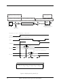
APPLICATION NOTE
MIPS R4000 Slew Rate Control Logic
for Output Buffers
Shabbir Latif
MIPS Technologies, Inc.
2011 N. Shoreline Blvd.
P. O. Box 7311
Mt. View, CA 94039-7311
Publication No.: AP001
Publication Date: July, 1992
MIPS Technologies, Inc. reserves the right to make changes to any products herein at any time without notice in order
to improve function or design. MIPS does not assume any liability arising out of the application or use of any product
or circuit described herein; neither does it convey any license under patent rights nor imply the rights of others.
Copyright 1992 by MIPS Technologies, Inc. No part of this document may be reproduced in any form or by any
means without the prior written consent of MIPS Technologies, Inc.
R4000 and R4400 are registered trademarks of MIPS Technologies, Inc.
The R4000 /R4400 is available from the following manufacturers:
Integrated Device Technology, Inc. (Attention - RISC Microprocessor Marketing)
2975 Stender Way
Santa Clara, CA 95052-8015
Tel: (408) 727 6116
LSI Logic Corporation (Attention - MIPS Division)
1551 McCarthy Blvd.
Milpitas, CA 95035
Tel: (408) 433 8000
NEC Corporation (Attention - Microcomputer Division)
401 Ellis St.
Mountain View, CA 94039
Tel: (415) 960-6000
Performance Semiconductor Corporation (Attention - Microprocessor Marketing)
610 E. Weddell Drive
Sunnyvale, CA 94089
Tel: (408) 734 9000
Siemens Components Inc. (Attention - Integrated Circuit Division)
10950 Tantau Ave.
Cupertino, CA 95014
Tel: (408) 777-4500
Toshiba Corporation
9740 Irvine Blvd.
Irvine, CA 92713
(714) 583-3000
Table of Contents
1. Overview ..................................................................................................5
2. Slew Rate Control for the Output Buffers in R4000 ..........................6
3. How to Set the “Drive off Delay” .........................................................9
4. Examples.................................................................................................13
Example 1 ..................................................................................................13
Example 2 ..................................................................................................13
Example 3 ..................................................................................................14
Example 4 ..................................................................................................14
5. Summary ................................................................................................15
6. References...............................................................................................16
7. Reader’s Comments ..............................................................................17
R4000 - Slew Rate Control Logic for the Output Buffers
R4000 - Slew Rate Control Logic for the Output Buffers
Overview
1
One of the largest causes of variation in voltage or noise on the GND and VCC
supplies is the switching of the Output Buffers. This variation in supply voltages
has two causes:
•
the large number of buffers that can switch at the same time
•
each buffer driving a large external load
Noise can be calculated using the formula
V = L(
∆i/ ∆t)
where V is the noise on the supplies, L is the inductance of the supply pin,
bonding wire, etc., and ∆i/ ∆t is the rate at which the current changes; this term is
directly related to how fast the load capacitor is charged or discharged by the
output drivers of the microprocessor.
The above variation or noise on the GND and VCC supplies can be reduced by
increasing the rise and fall times of the output drive. Although this reduces the
∆i/ ∆t term, it also increases the propagation delay time of the output signal to its
destination and care must be taken to ensure the resulting delay meets system
design requirements.
R4000 - Slew Rate Control Logic for the Output Buffers 5
Slew Rate Control for the Output Buffers in R4000
2
The R4000 has Slew Rate Control Logic with a negative feedback loop that adjusts
the output buffer drive (or slew rate) so that the output buffer is fast enough to
meet the system’s speed requirement, and no more, in order to minimize the noise
for that particular system. As shown in Figure 1, the feedback loop includes path
(A) from pins IO_Out to IO_In . This path represents the signal path with the
longest delay from the R4000 to any other external register which matches the load
and the transmission line effect on the PCB (see Reference 1). The Slew Rate
Control Logic drives a signal through the IO_Out output buffer and, using a
selectable clock, samples the return signal on the IO_In pin. If the signal arrives
earlier than the maximum acceptable delay, which is selected by the designer, the
Slew Rate Control Logic slows the speed of the IO_Out output buffer; if the signal
arrives later, it speeds up the IO_Out output buffer.
6
R4000 - Slew Rate Control Logic for the Output Buffers
Other Output
Buffers
Mode Bits<62:61>
EnblDPLL, EnblDPLLR
Mode Bits<52:50>
Drv0_50,Drv0_75,Drv1_00
Mode Bits<60:53>
InitP, InitN
R4000
Path B:
Path with the
longest delay
R
E
G
X_Out
X
X_In
R
E
G
IO_In
RClk
SampleClk
Path A:
Path matched to the
path with the
longest delay.
CntN<3:0>
CntP<3:0>
Slew Rate
Control
R
E
G
IO_Out
SClk
Figure 1: Overview of the Slew Rate Control Mechanism in R4000
The Slew Rate Control Logic uses the signals CntN<3:0> and CntP<3:0> to
control the N-channel and the P-channel devices, respectively, of the predrivers
to the final stage of the output buffers. This allows CntN<3:0> signals to adjust
the rising edge of the outputs and CntP<3:0> to adjust the falling edge, giving
16 independent states of control in each direction. All ones on CntN<3:0>
provides the fastest pullup rate and all zeros on CntP<3:0> provides the fastest
pulldown rate. The variation in the least significant bit (LSB), CntN<0> or
CntP<0> , provides the smallest resolution. Note that there is always some jitter
at the output due to the fact that the control mechanism is continuously trying to
converge to the programmed maximum adjustable delay value by switching the
state of the LSBs CntN<0> and CntP<0> . The signals, CntN<3:0> and
CntP<3:0> , that control the output buffer for IO_Out pin also control the output
buffers for the rest of the pins of the R4000. Thus, the slew rate of the rest of the
output buffers will vary in the same manner as the variation of the IO_OUT
buffer; however, the amount of variation will depend on the external loading on
each pin.
The R4000 has three modes for controlling the slew rates of the output buffers and
in turn minimizing the noise caused by ∆i/ ∆t. As shown in Table 1, these three
modes are selected by Mode Bits<62:61>, EnblDPLL and EnblDPLLR ,
respectively.
R4000 - Slew Rate Control Logic for the Output Buffers 7
Table 1: Modes of Operation for Controlling the Slew Rate
EnblDPLL EnblDPLLR
Modes of Operation
0
0
Keep the slew rate of the output drivers fixed as set by the Mode
Bits<60:57> and <56:53>, programmed during boot time.
0
1
Enable the mechanism to dynamically control the slew rate only
during ColdReset and thereafter retain the slew rate of the output
drivers.
1
X
(don’t care)
Enable the mechanism to dynamically control the slew rate during
ColdReset and Normal Operation.
The first mode in Table 1, which keeps the slew rate of the output buffer fixed, is
useful for the situation in which any jitter associated with the operation of the slew
rate control mechanism cannot be tolerated, and the variation in temperature and
supply voltage after ColdReset is expected to be small.
To dynamically control the slew rate, either during the ColdReset operation or
during both ColdReset and Normal operations, the R4000 does the following.
1.
It uses Mode Bits<60:57> and <56:53> (also referred as InitP and InitN ,
respectively), programmed during the boot time, to set the initial values of
CntN<3:0> and CntP<3:0> , which in turn sets the initial slew rate of the
output buffers.
2.
It uses the “drive-off” delay, programmed at boot time through Mode Bits
<52:50> (Drv1_00 , Drv0_75 or Drv0_50 ), as the maximum acceptable delay
of the data and, accordingly, selects the SampleClk to sample the IO_In as
shown in Figure 1. Table 2 shows the truth table for Mode Bits<52:50>; the
remaining combinations are reserved
3.
It uses the path between IO_Out pin and IO_In pin, as described earlier.
Table 2: The Truth Table for Mode Bits <52:50> , Setting Drive-off Delays
Mode
Drv1_00
Drv0_75
Drv_5
Drive-off time
Dynamic
0
0
1
0.50*T(2)
Dynamic
0
1
0
0.75*T(2)
Dynamic
1
0
0
1.00*T(2)
Fixed
X
X
X
Note 1
Notes: 1) The Fixed “Drive-off” Time Is Selected By Initn and Initp (Mode Bits<60:53>).
2) ‘T’ is the period of the Master clock (MasterClk).
To make the programmed delay value independent of system clock frequency
(MasterClk ), the delay value is specified in terms of a percentage of one cycle
time instead of a constant. Also, note that this mechanism is not affected by the
interface clocks divisor (Mode Bits<49:47>), it is always a fraction of one
(MasterClk ) cycle.
8
R4000 - Slew Rate Control Logic for the Output Buffers
How to Set the “Drive off Delay”
3
As mentioned in the previous section, for the dynamic control of the output buffer
slew rate, R4000 uses the “drive off delay” programmed by Mode Bits<52:50>
during boot time . This section explains how to determine the setting of these
mode bits. In general, a path is selected (Path B in Figure 1) with the longest delay
from the output pin to the output of the receiving data register (node X in Figure
1). Then, the transmission line effect and the capacitive loading of the IO_Out is
matched with the transmission line effect and the capacitive loading of Path B (see
Reference 1 for detail). Finally, after calculating at what time the SampleClk in
the Path A should be, the appropriate Mode Bits<52:50> (Drv1_00 , Drv0_75 or
Drv0_50 ) are selected.
Figure 2 shows the Path A again and the corresponding timing diagram with all
the delay components labelled. The equation of the delay TSS plus the clock jitter
TSSj in terms of the output buffer delay (tDO) is also shown (Equation 1). TSS is
the time from the rising edge of the SClk , which triggers the IO_Out, to the
SampleClk edge which latches the IO_In at a selected time. TSSj is the jitter of the
SampleClk with reference to the SClk. The TSSj could be both positive or
negative; however, a positive number is chosen because, in this case its affect is
worse than the affect of a negative number. tDOj is the jitter on the output caused
by the slew rate control logic which is continuously trying to converge to the
programmed “drive off” delay value by switching the state of the LSBs,
CntN<0> and CntP<0> .
Figure 3 shows Path B again and corresponding timing diagram with all the
delay components labelled. This path is an example of a signal path from the
R4000 to a receive-data register. This register could be part of external agent chip
or an individual component on the PCB. The rising edge of SClk drives the data,
and the rising edge of the RClkD latches the data into the register. TSR is the delay
between the RClk and the SClk , TSRD is delay between the RClkD and the SClk
and TSRj is the jitter on RClk or RClkD with respect to SClk . The TSRDj could be
a positive or a negative number; however, a negative number chosen because ,
in this case, its affect is worse than the affect of a positive number. The equation
of the delay time TSRD is shown in Equation 2 in Figure 3.
R4000 - Slew Rate Control Logic for the Output Buffers 9
TSSj=Sample Clk
Jitter
tDOj= Output Jitter due to
Slew Rate Control Logic
tDO=SClk to IO_Out Delay
tLi= Transmission Delay
tDSi= Input Set Up time to R4000
OBUFF
RECEIVER
REG
SAMPLE
REG
Transmission Line
Q
IO_Out
Q1
IO_In
IO_In1
Sample Clk
(Depend on the mode
bits<52:50>)
SClk
CntN<3:0>
CntP<3:0>
(Frequency of SClk < Frequency of MasterClk
SClk
(Frequency of SClk = Frequency of MasterClk)
SClk
TSS +TSSj
Sample Clk
tDOj
IO_Out
(The dotted waveforms show jitter only in
one, worst case, direction)
tDOj
IO_In
tDO
tLi
tDSi
Eq 1: TSS+ TSSj = tDO+ tLi + tDSi
Figure 2: Path from pins IO_Out to IO_In.
10
R4000 - Slew Rate Control Logic for the Output Buffers
tDOj= Output Jitter due to
Edge Control Logic
TSRj= Clock Jitter
tLx= Transmission Delay
tDO= SClk to X_Out Delay
tDSx= Input Set Up time to ext.logic
Receiver
OBuff
REG
Q
REG
Transmission Line
X_In
X_In1
X_Out
SClk
RClkD
CntN<3:0>
CntP<3:0>
tRD = Delay between RClk and RClkD
R4000
Transmission Line
RClk
Logic on the PCB
SClk
TSR-TSRj
tRD
RClk
TSRD-TSRj
RClkD
tDOj
X_Out
tDO
tLx
(dotted waveforms show jitter only
in one, worst case direction)
X_In
tDSx
Eq 2: TSRD-TSRj = tDO+ tDOj + tLx + tDSx
Figure 3: Representative Worst Case Path from R4000 to External Component
R4000 - Slew Rate Control Logic for the Output Buffers 11
X
If the capacitive load and the transmission line between the pins IO_Out and
IO_In are matched with the loading and the transmission line between X_Out
and X_In , then the output buffer delay, tDO, is equal in both the paths, and tLi =
tLx. Thus, deriving tDO from the Equation 2 and substituting into the equation
Equation 1, TSS can be derived to decide which of the Mode Bits Drv1_00 ,
Drv0_75 , or Drv0_50 needs to be selected.
Eq 3: DrvX_XX < TSS = TSRD - TSRj-tSSj + tDSi-tDSx - tDOj
12
R4000 - Slew Rate Control Logic for the Output Buffers
Examples
4
The following examples show how to set Mode Bits <52:50>.
Example 1
In a system with SysCkRatio (Mode bits<17:15>) set to 0 (Ref: 1) , the frequency
of RClk is equal to the frequency of MasterClk . If the delay, equal to the delay
between RClk and RClkD , is added between SyncIn pin and SyncOut pin, the
RClkD is locked to the MasterClk . But since RClkD leads SCLk and
MasterClk by 0.25*T; this means, TSRD is (0.75*T).
The R4000 AC specification (Ref.1) shows clock jitter = 0.5 ns, data set up time =
5.0 ns, and tDOj = 1 ns. Assuming tDSX = 7 ns, Equation 3 can be rewritten as:
Eq 4: TSS = (0.75*T) - 0.5ns - 0.5ns + 5 ns - 7ns - 1ns = 0.75*T - 4ns
Thus, for a 50 MHz system, TSS would be 11 ns; so Drv0_50 would be set to 1.
Example 2
In a system with SysCkRatio (Mode bits<17:15>) set to 0, the frequency of the
RClk is equal to the frequency of MasterClk . If the Sync_In pin is shorted to the
SyncOut pin, the RClk is locked to the MasterClk . Since RClk leads SClk and
MasterClk by 0.25*T; this means, TSRD is equal to (0.75*T + tRD), where tRD is the
delay between RClk and RClkD . Thus, Equation 4, from Example 1, can be
rewritten as,
TSS = (0.75*T + tRD) - 4ns
If tRD > 4ns then TSRD could be > (0.75*T+4ns), making TSS > 0.75*T; in which
case Drv0_75 is set to 1.
R4000 - Slew Rate Control Logic for the Output Buffers 13
Example 3
In a system with SysCkRatio set to 1, the frequency of RClk is two-thirds the
frequency of MasterClk , so TSRD is equal to (1.0*T) given in Example 1, and TSRD
is greater than (1.0*T) given in Example 2.
Thus, in the first example Drv0_75 is set to 1, and in the second example Drv1_00
is set to 1.
Example 4
Similarly, in the system with the SysCkRatio set to 2, the frequency of RClk is
half the frequency of MasterClk ; so Drv1_00 is set to 1 in Examples 1 and 2.
14
R4000 - Slew Rate Control Logic for the Output Buffers
Summary
5
The R4000 has Slew Rate Control Logic with negative feedback loop that adjusts
the output buffer drive so that the output buffer is only fast enough to meet the
system’s speed requirement, and no more, in order to minimize the noise for that
particular system. The maximum acceptable delay is programmed at the boot time
using the “drive-off” Mode Bits<52:50> (Drv1_00 , Drv0_75 or Drv0_50 ). It also
provides the flexibility to select whether to enable the control only during the
ColdReset time, or during the ColdReset time and the Normal operation, or to
select a fixed slew rate as programmed by the Mode Bits<60:53> (InitP and InitN ).
Some examples were shown in this document on how to select the “drive-off”
delay mode bits.
R4000 - Slew Rate Control Logic for the Output Buffers 15
References
Reference 1: MIPS R4000 Processor Interface Specification
Reference 2: MIPS R4000 Microprocessor User’s Manual
16
R4000 - Slew Rate Control Logic for the Output Buffers
Reader’s Comments
Please FAX your comments about this document to:
Anjaneya Thakar
Fax: (415) 390-6170
Address: 2011 N. Shoreline Blvd., P.O. Box 7311, Moutain View, CA 94039-7311
Areas of Improvement:
Errors:
Reader Information:
Name:
Company:
Address:
Phone:
FAX:
Thank you for your feedback.
R4000 - Slew Rate Control Logic for the Output Buffers 17