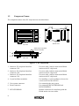
1
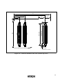
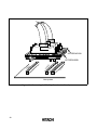
To all our customers
Regarding the change of names mentioned in the document, such as Hitachi
Electric and Hitachi XX, to Renesas Technology Corp.
The semiconductor operations of Mitsubishi Electric and Hitachi were transferred to Renesas
Technology Corporation on April 1st 2003. These operations include microcomputer, logic, analog
and discrete devices, and memory chips other than DRAMs (flash memory, SRAMs etc.)
Accordingly, although Hitachi, Hitachi, Ltd., Hitachi Semiconductors, and other Hitachi brand
names are mentioned in the document, these names have in fact all been changed to Renesas
Technology Corp. Thank you for your understanding. Except for our corporate trademark, logo and
corporate statement, no changes whatsoever have been made to the contents of the document, and
these changes do not constitute any alteration to the contents of the document itself.
Renesas Technology Home Page: http://www.renesas.com
Renesas Technology Corp.
Customer Support Dept.
April 1, 2003
SH7055 Evaluation Chip Board
(HS7055EBK81H)
for the E8000 Emulator
User’s Manual
HS7055EBK81HE(A)
Notice
When using this document, keep the following in mind:
1. This document may, wholly or partially, be subject to change without notice.
2. All rights are reserved: No one is permitted to reproduce or duplicate, in any form, the whole
or part of this document without Hitachi’s permission.
3. Hitachi will not be held responsible for any damage to the user that may result from accidents
or any other reasons during operation of the user’s unit according to this document.
4. Circuitry and other examples described herein are meant merely to indicate the characteristics
and performance of Hitachi’s semiconductor products. Hitachi assumes no responsibility for
any intellectual property claims or other problems that may result from applications based on
the examples described herein.
5. No license is granted by implication or otherwise under any patents or other rights of any third
party or Hitachi, Ltd.
6. MEDICAL APPLICATIONS: Hitachi’s products are not authorized for use in MEDICAL
APPLICATIONS without the written consent of the appropriate officer of Hitachi’s sales
company. Such use includes, but is not limited to, use in life support systems. Buyers of
Hitachi’s products are requested to notify the relevant Hitachi sales office when planning to use
the products in MEDICAL APPLICATIONS.
Preface
This manual describes how to connect and operate the EV-chip board. The EV-chip board
incorporates an evaluation chip for connection to a user system that uses the SH7055 with the
E8000 emulator.
Read and understand Sec. 3, “Preparation before Use” of the E8000 Emulator User’s Manual
before using this EV-chip board.
CAUTION
The EV-chip board is only for connection to a user
system that uses the SH7055 with the E8000 emulator.
It cannot be used for user systems that target other devices.
Contents
Section 1
1.1
1.2
Section 2
2.1
Preparation before Use ....................................................................4
Preparing the User System ................................................................................................ 4
2.1.1 Recommended Mounting Pad Dimensions of the User System ........................... 7
2.1.2 Connector Position on the User System ............................................................... 9
Section 3
3.1
Components .....................................................................................1
EV-Chip Board Components ............................................................................................ 1
Component Names ............................................................................................................ 2
Connecting the EV-Chip Board to the User System........................11
Connecting the EV-Chip Board to the User System.......................................................... 11
3.1.1 Connecting the Specified Connector .................................................................... 11
3.1.2 Connecting the Trace Cables to the EV-Chip Board............................................ 12
3.1.3 Connecting the EV-Chip Board to the User System Board.................................. 15
Figures
Figure 1.1
Figure 2.1
Figure 2.2
Figure 2.3
Figure 3.1
Figure 3.2
EV-Chip Board....................................................................................................... 2
Recommended Mounting Pad Dimensions............................................................. 8
Connector Position on the User System (Top View).............................................. 10
Component Height Restriction ............................................................................... 10
Connecting Trace Cables to the EV-Chip Board.................................................... 14
Connecting the EV-Chip Board to the User System............................................... 16
Tables
Table 1.1
Table 2.1
Table 2.1
Table 2.1
EV-chip Board Components................................................................................... 1
Pin Assignment of the HS7055EBK81H User Interface (UCN1) .......................... 5
Pin Assignment of the HS7055EBK81H User Interface (UCN2) .......................... 7
Pin Assignment of the HS7055EBK81H User Interface (UCN3) .......................... 6
Section 1 Components
1.1
EV-Chip Board Components
Table 1.1 lists the product components of the EV-chip board (HS7055EBK81H: 3 x 100-pin
connector type). Check all the components after unpacking.
Table 1.1
EV-chip Board Components
Item
Quantity
Remarks
EV-chip board
(HS7055EBK81H)
1
Consists of two boards.
• HS7055PWB20H (for connecting to the
E8000 station)
• HS7055PWB30H (3 x 100-pin connector)
Documentation
1
User’s manual for HS7055EBK81H (this manual)
Note: Use the specific connector (FX2-100P-1.27SVL manufactured by HIROSE ELECTRIC CO.,
LTD.) on the user system that is connected to the HS7055EBK81H.
1
1.2
Component Names
The component names of the EV-chip board are described below.
1
UC N2
UC N3
CN 3
U CN 1
Pin 1
CN 2
2
CN 1
3
X 1 X0
5
B ottom view
4
T op view
Station to E V -chip board
interface connectors
6
7
8
S ide view
Figure 1.1 EV-Chip Board
1. Station to EV-chip board interface
connector CN3:
For trace cable 3 which connects the E8000
station to the EV-chip board.
2. Station to EV-chip board interface
connector CN2:
For trace cable 2 which connects the E8000
station to the EV-chip board.
3. Station to EV-chip board interface
connector CN1:
For trace cable 1 which connects the E8000
station to the EV-chip board.
4. Crystal oscillator terminals:
For installing a crystal oscillator to be used as
a clock source for the SH7055.
5. User-system connector:
For connecting the user system.
6. Board connector:
For connecting HS7055PWB20H and
HS7055PWB30H.
7. HS7055PWB20H:
Includes connectors for interfacing with the
E8000 station via trace cables.
2
8. HS7055PWB30H:
Includes connectors for interfacing with the
user system.
3
Section 2 Preparation before Use
2.1
Preparing the User System
Table 2.1 lists the user interface pin assignment of the specific connector (FX2-100P-1.27SVL
manufactured by HIROSE ELECTRIC CO., LTD.) when the target MCU is the SH7055.
4
Table 2.1
Pin Assignment of the HS7055EBK81H User Interface (UCN1)
Pin No.
Pin Name
Pin No.
Pin Name
Pin No.
Pin Name
1
GND
35
PJ6/TIO2G
69
PK15/TO8P
2
GND
36
PJ7/TIO2H
70
GND
3
GND
37
GND
71
GND
4
GND
38
PJ8/TIO5C
72
GND
5
AN16
39
PJ9/TIO5D
73
GND
6
AN17
40
PJ10/TI9A
74
PL0/TI10
7
AN18
41
PJ11/TI9B
75
PL1/TIO11A/IRQ6
8
AN19
42
GND
76
PL2/TIO11B/IRQ7
9
GND
43
PJ12/TI9C
77
PL3/TCLKB
10
AN20
44
PJ13/TI9D
78
GND
11
AN21
45
PJ14/TI9E
79
PL4/ADTRG0
12
AN22
46
PJ15/TI9F
80
PL5/ADTRG1
13
AN23
47
GND
81
PL6/ADEND
14
GND
48
GND
82
PL7/SCK2
15
AN24
49
GND
83
GND
16
AN25
50
GND
84
PL8/SCK3
17
AN26
51
PK0/TO8A
85
PL9/SCK4/IRQ5
18
AN27
52
PK1/TO8B
86
PL10/HTxD
19
GND
53
PK2/TO8C
87
PL11/HRxD
20
AN28
54
PK3/TO8D
88
GND
21
AN29
55
GND
89
PL12/IRQ4
22
AN30
56
PK4/TO8E
90
PL13/IRQOUT
23
AN31
57
PK5/TO8F
91
GND
24
GND
58
PK6/TO8G
92
GND
25
GND
59
PK7/TO8H
93
GND
26
GND
60
GND
94
GND
27
GND
61
PK8/TO8I
95
Not connected
28
PJ0/TIO2A
62
PK9/TO8J
96
Not connected
29
PJ1/TIO2B
63
PK10/TO8K
97
Not connected
30
PJ2/TIO2C
64
PK11/TO8L
98
Not connected
31
PJ3/TIO2D
65
GND
99
Not connected
100
Not connected
32
GND
66
PK12/TO8M
33
PJ4/TIO2E
67
PK13/TO8N
34
PJ5/TIO2F
68
PK14/TO8O
5
6
Table 2.1
Pin Assignment of the HS7055EBK81H User Interface (UCN2)
Pin No.
Pin Name
Pin No.
Pin Name
Pin No.
Pin Name
1
AVCC
35
PA5/TIO3B
69
PC0/TxD1
2
GND
36
PA6/TIO3C
70
PC1/RxD1
3
AVREF
37
PA7/TIO3D
71
PC2/TxD2
4
AVREF
38
GND
72
PC3/RxD2
5
GND
39
PA8/TIO4A
73
PC4/IRQ4
6
GND
40
PA9/TIO4B
74
GND
7
AN0
41
PA10/TIO4C
75
PG0/PULS7/HRxD
8
AN1
42
PA11/TIO4D
76
PG1/IRQ1
9
AN2
43
GND
77
PG2/IRQ2/ADEND
10
AN3
44
PA12/TIO5A
78
PG3/IRQ3/ADTRG0
11
GND
45
PA13/TIO5B
79
GND
12
AN4
46
PA14/TxD0
80
TMS
13
AN5
47
PA15/RxD0
81
/TRST
14
AN6
48
GND
82
TDI
15
AN7
49
PB0/TO6A
83
TDO
16
GND
50
PB1/TO6B
84
TCK
17
AN8
51
PB2/TO6C
85
GND
18
AN9
52
PB3/TO6D
86
/AUDRST
19
AN10
53
GND
87
AUDMD
20
AN11
54
PB4/TO7A/TO8A
88
GND
21
GND
55
PB5/TO7B/TO8B
89
AUDD0
22
AN12
56
PB6/TO7C/TO8C
90
AUDD1
23
AN13
57
PB7/TO7D/TO8D
91
GND
24
AN14
58
GND
92
AUDD2
25
AN15
59
PB8/TxD3/TO8E
93
AUDD3
26
GND
60
PB9/RxD3/TO8F
94
GND
27
/WDTOVF
61
PB10/TxD4/HTxD/TO8G
95
AUDCK
28
GND
62
PB11/RxD4/HRxD/TO8H
96
/AUDSYNC
29
PA0/TIOA
63
GND
97
GND
30
PA1/TIOB
64
PB12/TCLKA
98
PVCC2
31
PA2/TIOC
65
PB13/SCK0
99
GND
32
PA3/TIOD
66
PB14/SCK1/TCLKB
100
FWE
33
GND
67
PB15/PULS5/SCK2
34
PA4/TIO3A
68
GND
7
8
Table 2.1
Pin Assignment of the HS7055EBK81H User Interface (UCN3)
Pin No.
Pin Name
Pin No.
Pin Name
Pin No.
Pin Name
1
NMI
35
MD1
69
GND
2
GND
36
MD2
70
PE7/A7
3
PVCC1
37
GND
71
PE6/A6
4
GND
38
EXTAL
72
PE5/A5
5
PH15/D15
39
GND
73
PE4/A4
6
PH14/D14
40
PF15/BREQ
74
GND
7
GND
41
PF14/BACK
75
PE3/A3
8
PH13/D13
42
PF13/CS3
76
PE2/A2
9
PH12/D12
43
PF12/CS2
77
PE1/A1
10
GND
44
GND
78
PE0/A0
11
PH11/D11
45
PF11/CS1
79
GND
12
PH10/D10
46
PF10/CS0
80
PD0/TIO1A
13
GND
47
PF9/RD
81
PD1/TIO1B
14
PH9/D9
48
PF8/WAIT
82
PD2/TIO1C
15
PH8/D8
49
GND
83
PD3/TIO1D
16
GND
50
PF7/WRH
84
GND
17
PH7/D7
51
PF6/WRL
85
PD4/TIO1E
18
PH6/D6
52
PF5/A21/POD
86
PD5/TIO1F
19
GND
53
PF4/A20
87
PD6/TIO1G
20
PH5/D5
54
GND
88
PD7/TIO1H
21
PH4/D4
55
PF3/A19
89
GND
22
GND
56
PF2/A18
90
PD8/PULS0
23
PH3/D3
57
PF1/A17
91
PD9/PULS1
24
PH2/D2
58
PF0/A16
92
PD10/PULS2
25
GND
59
GND
93
PD11/PULS3
26
PH1/D1
60
PE15/A15
94
GND
27
PH0/D0
61
PE14/A14
95
PD12/PULS4
28
GND
62
PE13/A13
96
PD13/PULS6/HTxD
29
CLK
63
PE12/A12
97
GND
30
GND
64
GND
98
GND(/UVCCSEL)
31
/RES
65
PE11/A11
99
GND
32
/STBY
66
PE10/A10
100
UVCC(3.3V)
33
GND
67
PE9/A9
34
MD0
68
PE8/A8
9
2.1.1
Recommended Mounting Pad Dimensions of the User System
Figure 2.1 shows the dimensions of the recommended mounting pad (footprint) and positioning
holes for the specific connector (FX2-100P-1.27SVL) manufactured by HIROSE ELECTRIC CO.,
LTD. The dimension tolerance is ±0.1 mm unless otherwise specified.
10
3.1
P =1.27±0.05
P in 1
0.8
φ2-1.9
3.3
U CN1
-0
+0.1
Pin 1
P ositioning hole
UCN 2
101.0
118.0
pad for fixing
10.0
P in 1
U CN3
62.23±0.10
67.31±0.10
71.95±0.10
U nit:m m
T olerance:±0.1m m
Figure 2.1 Recommended Mounting Pad Dimensions
11
2.1.2
Connector Position on the User System
CAUTION
Before connecting the connectors (FX2-100P-1.27SVL)
to the user system, check the location of pin 1 and the
connector shapes as shown in figures 2.2.
If the connector direction is incorrect, the EV-chip board
cannot be connected to the user system.
Figure 2.2 shows the direction of the connectors (FX2-100P-1.27SVL) on the user system.
Comply with the user system component height restriction shown in Figure 2.3 within the external
frame of the EV-chip board shown in Figure 2.2.
12
140.0
118.0
39.0
22.0
24.0
11.0
22.0
1
2
100
U CN 3
62.23±0.10
99
71.95±0.10
2
E xternal fram e of the E V -chip board
3.1
99
100
U CN 2
2
1
100
UCN1
99
95.0
1
3.3
U nit: m m
T olerance: ±0.1m m
Figure 2.2 Connector Position on the User System (Top View)
13
8.7
HS7055PWB30H
User system socket
FX2-100P-1.27SVL manufactured by
HIROSE ELECTRIC CO.,LTD
Figure 2.3 Component Height Restriction
14
User system boar
Unit: mm
Section 3 Connecting the EV-Chip Board to the User
System
3.1
Connecting the EV-Chip Board to the User System
3.1.1
Connecting the Specified Connector
This EV-chip board is designed exclusively for the specific connector (type number: FX2-100P1.27SVL) manufactured by HIROSE ELECTRIC CO., LTD. Therefore, it cannot be used with
other connectors.
• Positioning the IC socket
The connector FX2-100P-1.27SVL has two positioning pins. Insert the positioning pins of the
connector into the positioning holes of the user system board. Apply an epoxy adhesive to the
tips of the positioning pins of the connector to bond the connector to the user system board.
CAUTION
Before connecting the connectors to the user system,
check the location of pin 1 on both sides and the connector
shapes (UCN1 , UCN2 and UCN3).
• Mounting the connectors
Solder the FX2-100P-1.27SVL onto the user system. Use more solder than usual so that a fillet
is formed on the lead edge being soldered.
15
3.1.2
Connecting the Trace Cables to the EV-Chip Board
Always switch OFF the emulator and user system before
connecting or disconnecting any CABLES or sockets.
Failure to do so will result in a FIRE HAZARD and will
damage the user system and the emulator or will result in
PERSONAL INJURY. The USER PROGRAM will be LOST.
• EV-chip board condition at shipment
The EV-chip board is shipped with the HS7055PWB20H and HS7055PWB30H connected to
each other. When connecting the EV-chip board to the user system, do not separate the
HS7055PWB20H from the HS7055PWB30H.
CAUTION
Before connecting the EV-chip board to the user system,
confirm that the HS7055PWB20H and HS7055PWB30H
are firmly connected by lightly pushing the board.
• Connecting the trace cables to the E8000 station
Before connecting the trace cables to the HS7055PWB20H, connect the trace cables to the
E8000 station.
Note: At shipment, trace cables CN2 and CN3 to be connected to the E8000 station are
bound into a bundle, and trace cables CN1, CN2, and CN3 to be connected to the
EV-chip board are bound into a bundle to prevent an insertion error. For more
information on connecting the EV-Chip board to the E8000 station, refer to section
3.2.2, Connecting the EV-Chip Board, in the SH7055 E8000 Emulator User’s
Manual.
16
• Connecting the trace cables to the EV-chip board
Align the trace cables with the station to EV-chip board interface connectors CN1, CN2, and
CN3 on the EV-chip board. Confirm that each trace cable connected to a connector on the
E8000 station is also connected to its corresponding station to EV-chip board interface
connector on the EV-chip board. For the prevention of insertion errors, colors are specified on
the trace cable connectors and the corresponding EV-chip board interface connectors (CN1:
red, CN2: yellow, CN3: blue).
CAUTION
For the prevention of insertion errors, colors are specified on
the trace cable connectors and the corresponding EV-chip board
interface connectors.
E xam ple
T race cable screw s
C N 1:red
C N 3:blue
C N 2:yellow
C N 1:red
CN 3
CN 2
CN 1
CN 1
X1
T race cable connector
X0
T op view of the H S7055PW B 20H
17
Tighten the screws to connect the trace cable connectors to the station to EV-chip board
interface connectors while holding the HS7055PWB30H securely.
CN3
CN2
CN 1
H S 7055P W B 20H
H S 7055PW B 30H
Figure 3.1 Connecting Trace Cables to the EV-Chip Board
Make sure the connector shapes and numbers are
correctly matched when connecting the trace cables to the
station to EV-chip board interface connectors. Failure to
do so will result in a FIRE HAZARD.
18
3.1.3
Connecting the EV-Chip Board to the User System Board
• Connecting the EV-chip board to the user system board
Check the location of the FX2-100P-1.27SVL on the user system. Align the connectors on the
HS7055PWB30H of the EV-chip board with those on the user system board, and insert the
connectors.
CAUTION
Forcefully connecting the EV-chip board will apply
stress to the soldered connectors on the user system,
causing cracks in the solder. Gradually push the EV-chip
board repeatedly so that no cracks occur in the soldered
section of the connectors.
19
CN3
CN2
CN1
H S7055P W B 20H
U
CN
1
N2
C
U
U
C
N3
H S 7055PW B 30H
U sersystem
Figure 3.2 Connecting the EV-Chip Board to the User System
20