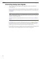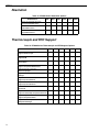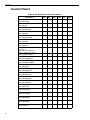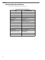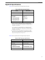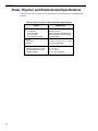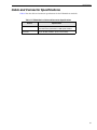
1
Title Page
UM-18221-L
DT9820 Series
User’s Manual
Copyright Page
Eleventh Edition
April, 2010
Copyright © 2001 - 2010 by Data Translation, Inc.
All rights reserved.
Information furnished by Data Translation, Inc. is believed to be
accurate and reliable; however, no responsibility is assumed by
Data Translation, Inc. for its use; nor for any infringements of
patents or other rights of third parties which may result from its
use. No license is granted by implication or otherwise under any
patent rights of Data Translation, Inc.
Use, duplication, or disclosure by the United States Government
is subject to restrictions as set forth in subparagraph (c)(1)(ii) of
the Rights in Technical Data and Computer software clause at 48
C.F.R, 252.227-7013, or in subparagraph (c)(2) of the Commercial
Computer Software - Registered Rights clause at 48 C.F.R.,
52-227-19 as applicable. Data Translation, Inc., 100 Locke Drive,
Marlboro, MA 01752.
Data Translation, Inc.
100 Locke Drive
Marlboro, MA 01752-1192
(508) 481-3700
www.datatranslation.com
Fax: (508) 481-8620
E-mail: [email protected]
Data Translation® is a registered trademark of Data Translation,
Inc. DT-Open LayersTM, DT-Open Layers for .NET Class
LibraryTM, DataAcq SDKTM, LV-LinkTM, and DTx-EZTM are
trademarks of Data Translation, Inc.
All other brand and product names are trademarks or registered
trademarks of their respective companies.
FCC
Page
Radio and Television Interference
This equipment has been tested and found to comply with CISPR EN55022 Class A and
EN61000-6-1 requirements and also with the limits for a Class A digital device, pursuant to
Part 15 of the FCC Rules. These limits are designed to provide reasonable protection against
harmful interference when the equipment is operated in a commercial environment. This
equipment generates, uses, and can radiate radio frequency energy and, if not installed and
used in accordance with the instruction manual, may cause harmful interference to radio
communications. Operation of this equipment in a residential area is likely to cause harmful
interference, in which case the user will be required to correct the interference at his own
expense.
Changes or modifications to this equipment not expressly approved by Data Translation could
void your authority to operate the equipment under Part 15 of the FCC Rules.
Note: This product was verified to meet FCC requirements under test conditions that
included use of shielded cables and connectors between system components. It is important
that you use shielded cables and connectors to reduce the possibility of causing interference
to radio, television, and other electronic devices.
Canadian Department of Communications Statement
This digital apparatus does not exceed the Class A limits for radio noise emissions from
digital apparatus set out in the Radio Interference Regulations of the Canadian Department of
Communications.
Le présent appareil numérique n’émet pas de bruits radioélectriques dépassant les limites
applicables aux appareils numériques de la class A prescrites dans le Règlement sur le
brouillage radioélectrique édicté par le Ministère des Communications du Canada.
Table of Contents
Table of Contents
About this Manual . . . . . . . . . . . . . . . . . . . . . . . . . . . . . . . . . . . . . . . . . . . . . . . . . . . . . . 9
Intended Audience. . . . . . . . . . . . . . . . . . . . . . . . . . . . . . . . . . . . . . . . . . . . . . . . . . . . . . . . . . . . . 9
How this Manual is Organized . . . . . . . . . . . . . . . . . . . . . . . . . . . . . . . . . . . . . . . . . . . . . . . . . . 9
Conventions Used in this Manual . . . . . . . . . . . . . . . . . . . . . . . . . . . . . . . . . . . . . . . . . . . . . . . 10
Related Information . . . . . . . . . . . . . . . . . . . . . . . . . . . . . . . . . . . . . . . . . . . . . . . . . . . . . . . . . . . 10
Where To Get Help. . . . . . . . . . . . . . . . . . . . . . . . . . . . . . . . . . . . . . . . . . . . . . . . . . . . . . . . . . . . 11
Chapter 1: Overview . . . . . . . . . . . . . . . . . . . . . . . . . . . . . . . . . . . . . . . . . . . . . . . . . . . 13
Features . . . . . . . . . . . . . . . . . . . . . . . . . . . . . . . . . . . . . . . . . . . . . . . . . . . . . . . . . . . . . . . . . . . . . 14
Supported Software . . . . . . . . . . . . . . . . . . . . . . . . . . . . . . . . . . . . . . . . . . . . . . . . . . . . . . . . . . 15
Accessories . . . . . . . . . . . . . . . . . . . . . . . . . . . . . . . . . . . . . . . . . . . . . . . . . . . . . . . . . . . . . . . . . . 16
Getting Started Procedure. . . . . . . . . . . . . . . . . . . . . . . . . . . . . . . . . . . . . . . . . . . . . . . . . . . . . . 17
Part 1: Getting Started . . . . . . . . . . . . . . . . . . . . . . . . . . . . . . . . . . . . . 19
Chapter 2: Installing a Module . . . . . . . . . . . . . . . . . . . . . . . . . . . . . . . . . . . . . . . . . . . 21
Unpacking . . . . . . . . . . . . . . . . . . . . . . . . . . . . . . . . . . . . . . . . . . . . . . . . . . . . . . . . . . . . . . . . . . 23
Attaching Modules to the Computer. . . . . . . . . . . . . . . . . . . . . . . . . . . . . . . . . . . . . . . . . . . . . 24
Connecting Directly to the Host Computer . . . . . . . . . . . . . . . . . . . . . . . . . . . . . . . . . . . 24
Connecting to a Self-Powered USB Hub . . . . . . . . . . . . . . . . . . . . . . . . . . . . . . . . . . . . . . 25
Chapter 3: Configuring the Device Driver . . . . . . . . . . . . . . . . . . . . . . . . . . . . . . . . . . 27
Chapter 4: Configuring and Attaching the Screw Terminal Panel . . . . . . . . . . . . . . 31
Configuring the STP9820 . . . . . . . . . . . . . . . . . . . . . . . . . . . . . . . . . . . . . . . . . . . . . . . . . . . . . . 33
Attaching the STP9820 . . . . . . . . . . . . . . . . . . . . . . . . . . . . . . . . . . . . . . . . . . . . . . . . . . . . . . . . 34
Chapter 5: Wiring Signals . . . . . . . . . . . . . . . . . . . . . . . . . . . . . . . . . . . . . . . . . . . . . . . 37
Preparing to Wire Signals . . . . . . . . . . . . . . . . . . . . . . . . . . . . . . . . . . . . . . . . . . . . . . . . . . . . . . 39
Connecting Analog Input Signals . . . . . . . . . . . . . . . . . . . . . . . . . . . . . . . . . . . . . . . . . . . . . . . 42
Connecting Analog Output Signals . . . . . . . . . . . . . . . . . . . . . . . . . . . . . . . . . . . . . . . . . . . . . 45
Connecting Digital Input Signals . . . . . . . . . . . . . . . . . . . . . . . . . . . . . . . . . . . . . . . . . . . . . . . 46
Connecting Digital Output Signals . . . . . . . . . . . . . . . . . . . . . . . . . . . . . . . . . . . . . . . . . . . . . . 47
Chapter 6: Verifying the Operation of a Module . . . . . . . . . . . . . . . . . . . . . . . . . . . . . 49
Running the Quick DataAcq Application . . . . . . . . . . . . . . . . . . . . . . . . . . . . . . . . . . . . . . . . 51
Testing Single-Value Analog Input . . . . . . . . . . . . . . . . . . . . . . . . . . . . . . . . . . . . . . . . . . . . . . 52
Testing Single-Value Analog Output . . . . . . . . . . . . . . . . . . . . . . . . . . . . . . . . . . . . . . . . . . . . 53
Testing Continuous Analog Input . . . . . . . . . . . . . . . . . . . . . . . . . . . . . . . . . . . . . . . . . . . . . . 54
Testing Single-Value Digital Input . . . . . . . . . . . . . . . . . . . . . . . . . . . . . . . . . . . . . . . . . . . . . . 55
Testing Single-Value Digital Output . . . . . . . . . . . . . . . . . . . . . . . . . . . . . . . . . . . . . . . . . . . . . 56
5
Contents
Part 2: Using Your Module. . . . . . . . . . . . . . . . . . . . . . . . . . . . . . . . . . 57
Chapter 7: Principles of Operation . . . . . . . . . . . . . . . . . . . . . . . . . . . . . . . . . . . . . . . 59
Analog Input Features . . . . . . . . . . . . . . . . . . . . . . . . . . . . . . . . . . . . . . . . . . . . . . . . . . . . . . . . 61
Input Resolution . . . . . . . . . . . . . . . . . . . . . . . . . . . . . . . . . . . . . . . . . . . . . . . . . . . . . . . . . . 61
Analog Input Channels . . . . . . . . . . . . . . . . . . . . . . . . . . . . . . . . . . . . . . . . . . . . . . . . . . . . 61
Input Ranges and Gains . . . . . . . . . . . . . . . . . . . . . . . . . . . . . . . . . . . . . . . . . . . . . . . . . . . 61
A/D Sample Clock . . . . . . . . . . . . . . . . . . . . . . . . . . . . . . . . . . . . . . . . . . . . . . . . . . . . . . . . 62
Triggers . . . . . . . . . . . . . . . . . . . . . . . . . . . . . . . . . . . . . . . . . . . . . . . . . . . . . . . . . . . . . . . . . 63
Analog Input Conversion Modes . . . . . . . . . . . . . . . . . . . . . . . . . . . . . . . . . . . . . . . . . . . 64
Data Format . . . . . . . . . . . . . . . . . . . . . . . . . . . . . . . . . . . . . . . . . . . . . . . . . . . . . . . . . . . . . 65
Converting an Offset Code to a Voltage . . . . . . . . . . . . . . . . . . . . . . . . . . . . . . . . . . 65
Converting a Twos Complement Code to a Voltage . . . . . . . . . . . . . . . . . . . . . . . . 66
Data Transfer . . . . . . . . . . . . . . . . . . . . . . . . . . . . . . . . . . . . . . . . . . . . . . . . . . . . . . . . . . . . . 67
Error Conditions . . . . . . . . . . . . . . . . . . . . . . . . . . . . . . . . . . . . . . . . . . . . . . . . . . . . . . . . . . 67
Synchronizing A/D Subsystems. . . . . . . . . . . . . . . . . . . . . . . . . . . . . . . . . . . . . . . . . . . . . 67
Synchronizing the Triggers . . . . . . . . . . . . . . . . . . . . . . . . . . . . . . . . . . . . . . . . . . . . . 67
Synchronizing the Clocks . . . . . . . . . . . . . . . . . . . . . . . . . . . . . . . . . . . . . . . . . . . . . . 68
Analog Output Features . . . . . . . . . . . . . . . . . . . . . . . . . . . . . . . . . . . . . . . . . . . . . . . . . . . . . . . 69
Output Resolution . . . . . . . . . . . . . . . . . . . . . . . . . . . . . . . . . . . . . . . . . . . . . . . . . . . . . . . . 69
Analog Output Channels . . . . . . . . . . . . . . . . . . . . . . . . . . . . . . . . . . . . . . . . . . . . . . . . . . 69
Output Ranges and Gains . . . . . . . . . . . . . . . . . . . . . . . . . . . . . . . . . . . . . . . . . . . . . . . . . . 69
Conversion Modes . . . . . . . . . . . . . . . . . . . . . . . . . . . . . . . . . . . . . . . . . . . . . . . . . . . . . . . . 69
Data Format . . . . . . . . . . . . . . . . . . . . . . . . . . . . . . . . . . . . . . . . . . . . . . . . . . . . . . . . . . . . . 70
Digital I/O Features . . . . . . . . . . . . . . . . . . . . . . . . . . . . . . . . . . . . . . . . . . . . . . . . . . . . . . . . . . 71
Digital I/O Lines . . . . . . . . . . . . . . . . . . . . . . . . . . . . . . . . . . . . . . . . . . . . . . . . . . . . . . . . . 71
Resolution . . . . . . . . . . . . . . . . . . . . . . . . . . . . . . . . . . . . . . . . . . . . . . . . . . . . . . . . . . . . . . . 71
Operation Modes . . . . . . . . . . . . . . . . . . . . . . . . . . . . . . . . . . . . . . . . . . . . . . . . . . . . . . . . . 71
Chapter 8: Supported Device Driver Capabilities. . . . . . . . . . . . . . . . . . . . . . . . . . . . 73
Data Flow and Operation Options. . . . . . . . . . . . . . . . . . . . . . . . . . . . . . . . . . . . . . . . . . . . . . . 75
Buffering . . . . . . . . . . . . . . . . . . . . . . . . . . . . . . . . . . . . . . . . . . . . . . . . . . . . . . . . . . . . . . . . . . . . 76
Triggered Scan Mode . . . . . . . . . . . . . . . . . . . . . . . . . . . . . . . . . . . . . . . . . . . . . . . . . . . . . . . . . . 76
Data Encoding. . . . . . . . . . . . . . . . . . . . . . . . . . . . . . . . . . . . . . . . . . . . . . . . . . . . . . . . . . . . . . . . 76
Channels . . . . . . . . . . . . . . . . . . . . . . . . . . . . . . . . . . . . . . . . . . . . . . . . . . . . . . . . . . . . . . . . . . . . 77
Gain . . . . . . . . . . . . . . . . . . . . . . . . . . . . . . . . . . . . . . . . . . . . . . . . . . . . . . . . . . . . . . . . . . . . . . . . 77
Ranges . . . . . . . . . . . . . . . . . . . . . . . . . . . . . . . . . . . . . . . . . . . . . . . . . . . . . . . . . . . . . . . . . . . . . . 77
Resolution . . . . . . . . . . . . . . . . . . . . . . . . . . . . . . . . . . . . . . . . . . . . . . . . . . . . . . . . . . . . . . . . . . . 78
Thermocouple and RTD Support. . . . . . . . . . . . . . . . . . . . . . . . . . . . . . . . . . . . . . . . . . . . . . . . 78
IEPE Support. . . . . . . . . . . . . . . . . . . . . . . . . . . . . . . . . . . . . . . . . . . . . . . . . . . . . . . . . . . . . . . . . 79
Triggers . . . . . . . . . . . . . . . . . . . . . . . . . . . . . . . . . . . . . . . . . . . . . . . . . . . . . . . . . . . . . . . . . . . . . 80
Clocks . . . . . . . . . . . . . . . . . . . . . . . . . . . . . . . . . . . . . . . . . . . . . . . . . . . . . . . . . . . . . . . . . . . . . . . 81
6
Contents
Counter/Timers . . . . . . . . . . . . . . . . . . . . . . . . . . . . . . . . . . . . . . . . . . . . . . . . . . . . . . . . . . . . . . 82
Chapter 9: Calibration . . . . . . . . . . . . . . . . . . . . . . . . . . . . . . . . . . . . . . . . . . . . . . . . . . 83
Running the Calibration Utility . . . . . . . . . . . . . . . . . . . . . . . . . . . . . . . . . . . . . . . . . . . . . . . . 85
Calibrating the Analog Output Subsystem . . . . . . . . . . . . . . . . . . . . . . . . . . . . . . . . . . . . . . . 86
Chapter 10: Troubleshooting . . . . . . . . . . . . . . . . . . . . . . . . . . . . . . . . . . . . . . . . . . . . 87
General Checklist . . . . . . . . . . . . . . . . . . . . . . . . . . . . . . . . . . . . . . . . . . . . . . . . . . . . . . . . . . . . . 88
Technical Support . . . . . . . . . . . . . . . . . . . . . . . . . . . . . . . . . . . . . . . . . . . . . . . . . . . . . . . . . . . . 90
If Your Module Needs Factory Service . . . . . . . . . . . . . . . . . . . . . . . . . . . . . . . . . . . . . . . . . . . 91
Appendix A: Specifications . . . . . . . . . . . . . . . . . . . . . . . . . . . . . . . . . . . . . . . . . . . . . 93
Analog Input Specifications . . . . . . . . . . . . . . . . . . . . . . . . . . . . . . . . . . . . . . . . . . . . . . . . . . . . 94
Analog Output Specifications. . . . . . . . . . . . . . . . . . . . . . . . . . . . . . . . . . . . . . . . . . . . . . . . . . . 96
Digital I/O Specifications . . . . . . . . . . . . . . . . . . . . . . . . . . . . . . . . . . . . . . . . . . . . . . . . . . . . . . 97
Power, Physical, and Environmental Specifications . . . . . . . . . . . . . . . . . . . . . . . . . . . . . . . . 98
Cable and Connector Specifications . . . . . . . . . . . . . . . . . . . . . . . . . . . . . . . . . . . . . . . . . . . . . 99
Regulatory Specifications . . . . . . . . . . . . . . . . . . . . . . . . . . . . . . . . . . . . . . . . . . . . . . . . . . . . . 100
Appendix B: Connector Pin Assignments . . . . . . . . . . . . . . . . . . . . . . . . . . . . . . . . 101
Connector J1 on the DT9820 Series . . . . . . . . . . . . . . . . . . . . . . . . . . . . . . . . . . . . . . . . . . . . . 102
Screw Terminal Assignments of the STP9820 . . . . . . . . . . . . . . . . . . . . . . . . . . . . . . . . . . . . 103
Appendix C: Using Your Own Screw Terminal Panel . . . . . . . . . . . . . . . . . . . . . . . 105
Analog Inputs . . . . . . . . . . . . . . . . . . . . . . . . . . . . . . . . . . . . . . . . . . . . . . . . . . . . . . . . . . . . . . 107
Analog Outputs . . . . . . . . . . . . . . . . . . . . . . . . . . . . . . . . . . . . . . . . . . . . . . . . . . . . . . . . . . . . . 108
Digital Inputs . . . . . . . . . . . . . . . . . . . . . . . . . . . . . . . . . . . . . . . . . . . . . . . . . . . . . . . . . . . . . . . 109
Digital Outputs . . . . . . . . . . . . . . . . . . . . . . . . . . . . . . . . . . . . . . . . . . . . . . . . . . . . . . . . . . . . . 110
Index . . . . . . . . . . . . . . . . . . . . . . . . . . . . . . . . . . . . . . . . . . . . . . . . . . . . . . . . . . . . . . . 111
7
Contents
8
About this Manual
This manual describes how to install and set up your DT9820 Series module and DT9820
Series device driver, and verify that your module is working properly.
This manual also describes the features of the DT9820 Series modules, the capabilities of the
DT9820 Series Device Driver, and how to program the DT9820 Series modules using the
DT-Open Layers for .NET Class Library™ software. Troubleshooting and calibration
information is also provided.
Note: For information on checking system requirements, installing the software, and
viewing the documentation, refer to the README file on the OMNI CD.
For more information on the class library, refer to the DT-Open Layers for .NET Class Library
User’s Manual. If you are using the DataAcq SDK or a software application to program your
device, refer to the documentation for that software for more information.
Intended Audience
This document is intended for engineers, scientists, technicians, or others responsible for
using and/or programming the DT9820 Series modules for data acquisition operations in the
Microsoft® Windows® XP, Windows Vista®, or Windows 7 operating systems. It is assumed
that you have some familiarity with data acquisition principles and that you understand your
application.
How this Manual is Organized
This manual is organized as follows:
• Chapter 1, “Overview,” describes the major features of the modules, as well as the
supported software and accessories for the modules, and provides an overview of the
DT9820 Series getting started procedure.
• Chapter 2, “Installing a Module,” describes how to install the DT9820 Series module.
• Chapter 3, “Configuring the Device Driver,” describes how to configure the device driver
and the module.
• Chapter 4, “Configuring and Attaching the Screw Terminal Panel,” describes how to
configure the STP9820 screw terminal and attach it to a DT9820 Series module.
• Chapter 5, “Wiring Signals,” describes how to wire signals to a DT9820 Series module.
• Chapter 6, “Verifying the Operation of a Module,” describes how to verify the operation
of a DT9820 Series module with the Quick DataAcq application.
• Chapter 7, “Principles of Operation,” describes all of the features of the modules and how
to use them in your application.
9
About this Manual
• Chapter 8, “Supported Device Driver Capabilities,” lists the data acquisition subsystems
and the associated features accessible using the DT9820 Series Device Driver.
• Chapter 9, “Calibration,” describes how to calibrate the analog output circuitry of the
DT9822 modules.
• Chapter 10, “Troubleshooting,” provides information that you can use to resolve problems
with the modules and the device driver, should they occur.
• Appendix A, “Specifications,” lists the specifications of the modules.
• Appendix B, “Connector Pin Assignments,” shows the pin assignments for the connectors
and the screw terminal assignments for the modules.
• Appendix C, “Using Your Own Screw Terminal Panel,” describes additional
considerations to keep in mind when designing your own screw terminal panel for use
with a DT9820 Series board.
• An index completes this manual.
Conventions Used in this Manual
The following conventions are used in this manual:
• Notes provide useful information or information that requires special emphasis, cautions
provide information to help you avoid losing data or damaging your equipment, and
warnings provide information to help you avoid catastrophic damage to yourself or your
equipment.
• Items that you select or type are shown in bold.
Related Information
Refer to the following documents for more information on using the DT9820 Series modules:
• Benefits of the Universal Serial Bus for Data Acquisition. This white paper describes why USB
is an attractive alternative for data acquisition. It is available on the Data Translation web
site (www.datatranslation.com).
• Measure Foundry Manual (UM-19298) and online help. These documents describe how to
use Measure Foundry™ to build drag-and-drop test and measurement applications for
Data Translation® data acquisition devices without programming.
• DT-Open Layers for .NET User’s Manual (UM-22161). For programmers who are developing
their own application programs using Visual C# or Visual Basic .NET, this manual
describes how to use the DT-Open Layers for .NET Class Library to access the capabilities
of Data Translation data acquisition devices.
• DataAcq SDK User’s Manual (UM-18326). For programmers who are developing their own
application programs using the Microsoft C compiler, this manual describes how to use
the DT-Open Layers DataAcq SDKTM to access the capabilities of Data Translation data
acquisition devices.
• DTx-EZ Getting Started Manual (UM-15428). This manual describes how to use the ActiveX
controls provided in DTx-EZTM to access the capabilities of Data Translation data
acquisition devices in Microsoft Visual Basic® or Visual C++®.
10
About this Manual
• LV-Link Online Help. This help file describes how to use LV-Link™ with the LabVIEW™
graphical programming language to access the capabilities of Data Translation data
acquisition devices.
Where To Get Help
Should you run into problems installing or using a DT9820 Series module, the Data
Translation Technical Support Department is available to provide technical assistance. Refer to
Chapter 10 starting on page 87 for more information. If you are outside the United States or
Canada, call your local distributor, whose number is listed on Data Translation’s web site
(www.datatranslation.com).
11
About this Manual
12
1
Overview
Features . . . . . . . . . . . . . . . . . . . . . . . . . . . . . . . . . . . . . . . . . . . . . . . . . . . . . . . . . . . . . . . . . . . . . 14
Supported Software . . . . . . . . . . . . . . . . . . . . . . . . . . . . . . . . . . . . . . . . . . . . . . . . . . . . . . . . . . . 15
Accessories . . . . . . . . . . . . . . . . . . . . . . . . . . . . . . . . . . . . . . . . . . . . . . . . . . . . . . . . . . . . . . . . . . 16
Getting Started Procedure. . . . . . . . . . . . . . . . . . . . . . . . . . . . . . . . . . . . . . . . . . . . . . . . . . . . . . 17
13
Chapter 1
Features
The DT9820 Series is a high-resolution (24-bit) family of data acquisition modules for the
Universal Serial Bus (USB).
Most computers have two or more USB ports that allow direct connection to USB devices. You
can expand the number of USB devices attached to a single USB port by using expansion
hubs. DT9820 Series modules are part of the high-power, bus-powered USB class; therefore,
the modules do not require external power, but the expansion hubs do require external power.
DT9820 Series modules reside outside of the PC and install with a single cable to ease
installation. Modules can be “hot swapped,” or plugged and unplugged while the PC is on,
making them useful for many data acquisition applications.
The DT9820 Series includes the DT9821 and DT9822. Table 1 lists the key features of each
module.
Table 1: Key Features Among the DT9820 Series
Analog Input
Sample Rate
Module
Analog
Inputs
60 Hz
Analog
Outputs
50 Hz
Digital I/O
Lines
DT9821
4 with 24-bit
resolutiona
960 Hz
800 Hz
0
8 inputb,
8 output
DT9822
4 with 24-bit
resolutiona
960 Hz
800 Hz
2, 16-bit
resolution
8 inputb,
8 output
a. The channels are configured as differential.
b. Digital input lines 0 to 3 can be used to start A/D conversions. Digital input lines 4 to 7 can
be used to stop A/D conversions.
Both DT9820 Series modules share the following major features:
• USB compatibility
• Software configurable termination resistance for differential analog inputs on a
channel-by-channel basis
• Input gains of 1, 2, 4, 8, 16, 32, and 64
• Continuously paced analog input operations
• One 8-bit digital input port; high-to-low transitions on digital input lines 0 to 3 can start
A/D conversions on A/D subsystems 0 to 3; high-to-low transitions on digital input lines
4 to 7 can stop A/D conversions on A/D subsystems 0 to 3
• One 8-bit digital output port; digital outputs can drive external solid-state relays
• Automatic software calibration of the analog I/O subsystems
14
Overview
Supported Software
The following software is available for use with the DT9820 Series modules:
• DT9820 Series Device Driver – This software is provided on the Data Acquisition OMNI
CD that is shipped with the module. The device driver allows you to use a DT9820 Series
module with any of the supported software packages or utilities.
• DT9820 Series Calibration Utility – This software is provided on the Data Acquisition
OMNI CD-ROM. The DT9820 Series Calibration Utility allows you to calibrate the analog
output circuitry of the DT9822 modules. The analog input circuitry is automatically
calibrated when the module is powered up. Refer to Chapter 9 starting on page 83 for
more information on this utility.
• Quick DataAcq application – This software is provided on the Data Acquisition OMNI
CD that is shipped with the module. The Quick DataAcq application provides a quick
way to get up and running using a DT9820 Series module. Using this application, you can
verify key features of the module, display data on the screen, and save data to disk.
• The quickDAQ application – An evaluation version of this .NET application is included
on the Data Acquisition OMNI CD. quickDAQ lets you acquire analog data from all
devices supported by DT-Open Layers for .NET software at high speed, plot it during
acquisition, analyze it, and/or save it to disk for later analysis.
• Measure Foundry – An evaluation version of this software is included on the Data
Acquisition OMNI CD. Measure Foundry is drag-and-drop test and measurement
application builder designed to give you top performance with ease-of-use development.
Order the full development version of this software package to develop your own
application using real hardware.
• DT-Open Layers for .NET Class Library – Use this class library if you want to use Visual
C# or Visual Basic for .NET to develop your own application software for a DT9820 Series
module using Visual Studio 2003 or Visual Studio 2005; the class library complies with the
DT-Open Layers standard.
• DataAcq SDK – Use the Data Acq SDK if you want to use Visual Studio 6.0 and Microsoft
C or C++ to develop your own application software for a DT9820 Series module using
Windows XP, Windows Vista, or Windows 7; the DataAcq SDK complies with the
DT-Open Layers standard.
• DTx-EZ – Use this optional software package if you want to use ActiveX controls to access
the capabilities of the DT9820 Series modules using Microsoft Visual Basic or Visual C++;
DTx-EZ complies with the DT-Open Layers standard.
• DAQ Adaptor for MATLAB – Data Translation’s DAQ Adaptor provides an interface
between the MATLAB Data Acquisition (DAQ) subsystem from The MathWorks and Data
Translation’s DT-Open Layers architecture.
• LV-Link – An evaluation version of LV-Link is included on the Data Acquisition OMNI
CD. Use this optional software package if you want to use the LabVIEW graphical
programming language to access the capabilities of the DT9820 Series modules.
Refer to the Data Translation web site (www.datatranslation.com) for more information on the
appropriate software package for your application.
15
Chapter 1
Accessories
The following accessories are provided for the DT9820 Series:
• EP365 – a 1.83-meter, USB cable that connects the USB connector of the DT9820 Series
module to the USB connector on the host computer. An EP365 cable is shipped with each
DT9820 Series module. In addition, if you want to buy additional USB cables, EP365 is
available as an accessory product for the DT9820 Series.
• STP9820 – a 100 mm x 160 mm screw terminal panel that connects to the DT9820 Series
module either directly or by using an EP777 cable. This screw terminal panel allows you
to connect all of the input and output connections that are supported by aDT9820 Series
module.
• EP777 – a 6-foot cable that connects the DT9820 Series module to the STP9820 screw
terminal panel.
16
Overview
Getting Started Procedure
The flow diagram shown in Figure 1 illustrates the steps needed to get started using the
DT9820 Series modules. This diagram is repeated in each getting started chapter; the shaded
area in the diagram shows you where you are in the getting started procedure.
Install the Module
(see Chapter 2 starting on page 21)
Configure the Device Driver
(see Chapter 3 starting on page 27)
Configure and Attach the Screw Terminal
Panel (see Chapter 4 starting on page 31)
Wire Signals
(see Chapter 5 starting on page 37)
Verify the Operation of the Module
(see Chapter 6 starting on page 49)
Figure 1: Getting Started Flow Diagram
17
Chapter 1
18
Part 1: Getting Started
2
Installing a Module
Unpacking . . . . . . . . . . . . . . . . . . . . . . . . . . . . . . . . . . . . . . . . . . . . . . . . . . . . . . . . . . . . . . . . . . . 23
Attaching Modules to the Computer. . . . . . . . . . . . . . . . . . . . . . . . . . . . . . . . . . . . . . . . . . . . . 24
21
Chapter 2
Install the Module
(this chapter)
Configure the Device Driver
(see Chapter 3 starting on page 27)
Configure and Attach the Screw Terminal
Panel (see Chapter 4 starting on page 31)
Wire Signals
(see Chapter 5 starting on page 37)
Verify the Operation of the Module
(see Chapter 6 starting on page 49)
22
Installing a Module
Unpacking
Open the shipping box and verify that the following items are present:
• DT9820 Series module
• EP365 USB cable
• Data Acquisition OMNI CD-ROM
If an item is missing or damaged, contact Data Translation. If you are in the United States, call
the Customer Service Department at (508) 481-3700, ext. 1323. An application engineer will
guide you through the appropriate steps for replacing missing or damaged items. If you are
located outside the United States, call your local distributor, listed on Data Translation’s web
site (www.datatranslation.com).
23
Chapter 2
Attaching Modules to the Computer
You can attach a DT9820 Series module to the host computer in one of two ways:
• Connect directly to a USB port of the host computer, described on page 24. Use this
method if one or two DT9820 Series modules are sufficient for your application.
• Connect to one or more self-powered USB hubs, described on page 25. Use this method if
your application requires more than two DT9820 Series modules connected to the host
computer.
You must install the device driver before connecting your DT9820 Series module(s) to the host
computer.
Note: DT9820 Series modules are low-power devices (using less than 500 mA); therefore,
they do not require external power supplies.
Also, the DT9820 Series modules are automatically calibrated when you power the module.
No calibration steps are required.
Connecting Directly to the Host Computer
Generally, host computers have two or more USB ports. These ports are completely
independent. To connect a DT9820 Series module directly to a USB port of the computer, do
the following:
1. Attach one end of the EP365 cable, which is shipped with the DT9820 Series module, to
the USB port on the module.
2. Attach the other end of the EP365 cable to one of the USB ports on the host computer, as
shown in Figure 2.
The operating system automatically detects the USB device and starts the Found New Hardware
wizard.
USB Ports
DT9820 Series
Modules
Host Computer
EP365 Cables
Figure 2: Attaching the DT9820 Series Module Directly
to the Host Computer
3. For Windows Vista:
a. Click Locate and install driver software (recommended).
The popup message "Windows needs your permission to continue" appears.
24
Installing a Module
b. Click Continue.
The Windows Security dialog box appears.
c.
Click Install this driver software anyway.
For Windows XP:
a. Click Next and/or Finish as required in the wizard.
Once the firmware is loaded, the wizard restarts to initiate the firmware to accept commands.
b. Click Next and/or Finish again.
Note: Windows 7 finds the device automatically.
4. Repeat these steps to attach another DT9820 Series module to the host computer, if
desired.
Note: You can unplug a module, and then plug it in again, if you wish, without causing
damage. This process is called hot-swapping.
Your application may take a few seconds to recognize a module once it is plugged back in.
Connecting to a Self-Powered USB Hub
Self-powered USB hubs are USB hubs that are powered by their own external power supply.
The practical number of DT9820 Series modules that you can connect to a single USB port
depends on the throughput you want to achieve.
Note: The bandwidth of the USB Ver. 1.1 bus is 12 Mbits/second. For each DT9820 Series
module, the maximum throughput is 960 Hz and each buffer is four bytes wide. Therefore, if
you want to achieve full throughput on each module, you should connect no more than four
DT9820 Series modules to a single USB Ver. 1.1 port.
To connect a DT9820 Series module to a self-powered USB hub, do the following:
1. Attach one end of the EP365 cable to the DT9820 Series module and the other end of the
EP365 cable to a self-powered USB hub.
2. Connect the power supply for the self-powered USB hub to an external power supply.
3. Connect the hub to the USB port on the host computer using another EP365 cable.
The operating system automatically detects the USB device and starts the Found New Hardware
wizard.
4. For Windows Vista:
a. Click Locate and install driver software (recommended).
The popup message "Windows needs your permission to continue" appears.
25
Chapter 2
b. Click Continue.
The Windows Security dialog box appears.
c.
Click Install this driver software anyway.
For Windows XP:
a. Click Next and/or Finish as required in the wizard.
Once the firmware is loaded, the wizard restarts to initiate the firmware to accept commands.
b. Click Next and/or Finish again.
Note: Windows 7 finds the device automatically.
5. Repeat these steps until you have attached the number of hubs and modules that you
desire. Refer to Figure 3.
The operating system automatically detects the USB devices as they are installed.
DT9820 Series Module
EP365 Cables
DT9820 Series Module
Host Computer
EP365 Cable
EP365 Cable
Self-Powered
USB Hubs
Power Supply
for Hub
DT9820 Series Module
DT9820 Series Module
EP365 Cables
Figure 3: Attaching DT9820 Series Modules
to the Host Computer Using Self-Powered USB Hubs
Note: You can unplug a module, and then plug it in again, if you wish, without causing
damage. This process is called hot-swapping.
Your application may take a few seconds to recognize a module once it is plugged back in.
26
3
Configuring the Device Driver
27
Chapter 3
Install the Module
(see Chapter 2 starting on page 21)
Configure the Device Driver
(this chapter)
Configure and Attach the Screw Terminal
Panel (see Chapter 4 starting on page 31)
Wire Signals
(see Chapter 5 starting on page 37)
Verify the Operation of the Module
(see Chapter 6 starting on page 49)
This chapter describes how to configure the DT9820 Series Device Driver.
To configure the device driver, do the following:
1. If you have not already done so, power up the host computer and all peripherals.
2. From the Control Panel, double-click the Open Layers Data Acquisition Control Panel
icon.
The Open Layers dialog box appears.
3. Click the DT9820 Series module that you want to configure, and then click Advanced.
The DT9820 Configuration dialog box appears.
4. We recommend that you select the 10k Ohm Resistor Terminations checkbox for each
analog input channel on the module. This ensures that 10 kΩ of bias return termination
resistance is used for the analog input channels. (This is the default configuration.) Bias
return termination resistance is particularly useful when your differential source is
floating.
5. Select whether the DT9820 Series module will be used in 60 Hz operations (the default), or
50 Hz operations (used primarily in Europe).
6. To continuously power the analog and/or digital outputs, select the Power Always On
checkbox. The DT9820 Series module will remain on even when you exit from the
applications that use the module.
If you want to shut down power to the module, you must uncheck this checkbox and
close the control panel. Once all applications that use this module are exited, the module
will power down. The module will remain off until you either run an application that uses
the module or click the Advanced button from the Open Layers Data Acquisition Control
Panel.
7. Click OK.
8. If you want to rename the module, click Edit Name; otherwise, go to step 10.
28
Configuring the Device Driver
9. Enter a new name for the module, and then click OK.
Note: This name is used to identify the module in all subsequent applications.
10. When you are finished configuring the module, click Close.
11. Repeat steps 3 to 10 for the other modules that you want to configure.
12. Close the Control Panel.
29
Chapter 3
30
4
Configuring and Attaching the Screw
Terminal Panel
Configuring the STP9820. . . . . . . . . . . . . . . . . . . . . . . . . . . . . . . . . . . . . . . . . . . . . . . . . . . . . . . 33
Attaching the STP9820. . . . . . . . . . . . . . . . . . . . . . . . . . . . . . . . . . . . . . . . . . . . . . . . . . . . . . . . . 34
31
Chapter 4
Install the Module
(see Chapter 2 starting on page 21)
Configure the Device Driver
(see Chapter 3 starting on page 27)
Configure and Attach the Screw Terminal
Panel (this chapter)
Wire Signals
(see Chapter 5 starting on page 37)
Verify the Operation of the Module
(see Chapter 6 starting on page 49)
Before you can wire signals to a DT9820 Series module, you first need to configure the
STP9820 screw terminal panel, and then attach the STP9820 to the DT9820 Series module.
Refer to Figure 4 for an illustration of the STP9820.
C1
J1
R1
R2
R4
R7
R9
R12
R14
R17
R19
1
R3
R5
R8
R10
R13
R15
R18
R20
U1
R22
R23
R24
R25
R26
R27
R28
R29
1
TB1
1
TB2
1
TB3
R6
R11
R16
R21
1
TB4
1
TB5
1
TB6
User-Configurable Resistors
Figure 4: STP9820 Screw Terminal Panel
32
Configuring and Attaching the Screw Terminal Panel
Configuring the STP9820
The STP9820 allows you to install a Toshiba TD62083AP (or equivalent) relay driver for use
with the digital output lines on the DT9820 Series module. This driver, which works only with
TTL digital output lines, allows the digital output lines of the DT9820 Series board to drive
most commercially available +5 V relays with up to 100 mA of current and +5 V of
user-supplied power.
CAUTION:
The external +5 V power supply voltage must not exceed 5.25 V or
damage may result to the DT9820 Series module.
A logic “1” switches the appropriate relay driver on. A logic “0” switches the appropriate
relay driver off.
If you wish to install a relay driver, do the following:
1. Remove resistors from locations R22 to R29.
2. Solder the relay driver in location U1 on the STP9820 while observing the correct polarity.
Continue with the next section to attach the STP9820 screw terminal panel to a DT9820 Series
module.
Note: Refer to page 47 for information on how to connect relays to the STP9820 once the
relay driver is installed.
33
Chapter 4
Attaching the STP9820
You can connect the STP9820 directly to the J1 connector on your DT9820 Series module, or
you can connect the STP9820 to the DT9820 Series module using the EP777 cable, which is
available from Data Translation.
Figure 5 illustrates these connection methods.
DT9820
Series
Module
J1
STP9820
Screw
J1 Terminal
Panel
or
DT9820
Series
Module
J1
EP777 Cable
STP9820
Screw
J1 Terminal
Panel
Figure 5: Attaching the STP9820 Screw Terminal Panel to a DT9820 Series Module
34
Configuring and Attaching the Screw Terminal Panel
Table 2 lists the pin assignments of the J1 connector on the DT9820 Series modules and on the
STP9820 screw terminal panel.
Table 2: Pin Assignments for Connector J1 on the DT9820 Series Module
and on the STP9820 Screw Terminal Panel
Pin
Signal Description
Pin
Signal Description
1
Isolated Digital Ground
2
Digital Output Line 3
3
Digital Output Line 2
4
Digital Output Line 1
5
Digital Output Line 0
6
Digital Input Line 3
7
Digital Input Line 2
8
Digital Input Line 1
9
Digital Input Line 0
10
+5 V Isolated Input/Outputa
11
Isolated Digital Ground
12
Isolated Analog Common
13
Analog Input Subsystem 03
14
Isolated Analog Common
15
Analog Input Subsystem 02
16
2.5 V Reference
17
Analog Input Subsystem 01
18
Isolated Analog Common
19
Analog Input Subsystem 00
20
Digital Output Line 7
21
Digital Output Line 6
22
Digital Output Line 5
23
Digital Output Line 4
24
Digital Input Line 7
25
Digital Input Line 6
26
Digital Input Line 5
27
Digital Input Line 4
28
Analog Output 0
29
Isolated Analog Common
30
Isolated Analog Common
31
Analog Input Subsystem 03 Return
32
Isolated Analog Common
33
Analog Input Subsystem 02 Return
34
Analog Output 1
35
Analog Input Subsystem 01 Return
36
Isolated Analog Common
37
Analog Input Subsystem 00 Return
a. +5 V output is available only when one of the subsystems is activated, which, in turn, activates
power to the module. You can externally power the +5 V isolated output signal. This allows
you to retain the last value that was written to the digital output lines when the DT9820 Series
module is in low-power mode.
35
Chapter 4
36
5
Wiring Signals
Preparing to Wire Signals . . . . . . . . . . . . . . . . . . . . . . . . . . . . . . . . . . . . . . . . . . . . . . . . . . . . . . 39
Connecting Analog Input Signals . . . . . . . . . . . . . . . . . . . . . . . . . . . . . . . . . . . . . . . . . . . . . . . 42
Connecting Analog Output Signals. . . . . . . . . . . . . . . . . . . . . . . . . . . . . . . . . . . . . . . . . . . . . . 45
Connecting Digital Input Signals. . . . . . . . . . . . . . . . . . . . . . . . . . . . . . . . . . . . . . . . . . . . . . . . 46
Connecting Digital Output Signals . . . . . . . . . . . . . . . . . . . . . . . . . . . . . . . . . . . . . . . . . . . . . . 47
37
Chapter 5
Install the Module
(see Chapter 2 starting on page 21)
Configure the Device Driver
(see Chapter 3 starting on page 27)
Configure and Attach the Screw Terminal
Panel (see Chapter 4 starting on page 31)
Wire Signals
(this page)
Verify the Operation of the Module
(see Chapter 6 starting on page 49)
38
Wiring Signals
Preparing to Wire Signals
Keep the following recommendations in mind when wiring signals to the DT9820 Series
modules:
• Follow standard ESD procedures when wiring signals to the module.
• Use individually shielded twisted-pair wire (size 14 to 26 AWG) when using the DT9820
Series module in highly noisy electrical environments.
• Separate power and signal lines by using physically different wiring paths or conduits.
• To avoid noise, do not locate the DT9820 Series modules and cabling next to sources that
produce high electromagnetic fields, such as large electric motors, power lines, solenoids,
and electric arcs, unless the signals are enclosed in a mumetal shield.
• Prevent electrostatic discharge to the I/O while the DT9820 Series modules are
operational.
• Connect all unused analog input channels to analog ground.
• When first installing the module, try wiring the signals as follows:
− Wire a function generator or a known voltage source to analog input subsystem 0
using the differential configuration.
− Wire an oscilloscope or voltage meter to analog output channel 0.
− Wire a digital input to digital input line 0.
− Wire a digital output to digital output line 0.
− Then, run the Quick DataAcq application (described in Chapter 6 starting on page 49)
to verify that the module is operating properly.
Once you have determined that the module is operating properly, wire the signals
according to your application’s requirements.
Note: Connector J1 is tied to the host computer’s chassis ground.
Table 3 lists the assignments of the screw terminals on the STP9820 screw terminal panel.
39
Chapter 5
Table 3: Screw Terminal Assignments of the STP9820
Screw Terminal Panel
Screw Terminal
Block
TB1
TB2
TB3
TB4
40
Terminal
Number
Terminal
Label
Signal Description
1
CH0H
Analog Input Subsystem 0 High
2
CH0L
Analog Input Subsystem 0 Low
3
AGND
Analog Ground
4
CH1H
Analog Input Subsystem 1 High
5
CH1L
Analog Input Subsystem 1 Low
6
AGND
Analog Ground
1
CH2H
Analog Input Subsystem 2 High
2
CH2L
Analog Input Subsystem 2 Low
3
AGND
Analog Ground
4
CH3H
Analog Input Subsystem 3 High
5
CH3L
Analog Input Subsystem 3 Low
6
AGND
Analog Ground
1
VREF
2.5 V Reference
2
AGND
Analog Ground
3
DAC0
Analog Output 0
4
DAC1
Analog Output 1
5
DGND
Digital Ground
6
+5VD
+5 Va
1
DOUT0
Digital Output 0
2
DOUT1
Digital Output 1
3
DOUT2
Digital Output 2
4
DOUT3
Digital Output 3
5
DOUT4
Digital Output 4
6
DOUT5
Digital Output 5
7
DOUT6
Digital Output 6
8
DOUT7
Digital Output 7
9
DGND
Digital Ground
Wiring Signals
Table 3: Screw Terminal Assignments of the STP9820
Screw Terminal Panel (cont.)
Screw Terminal
Block
TB5
Terminal
Number
Terminal
Label
Signal Description
1
DIN0
Digital Input 0
2
DIN1
Digital Input 1
3
DIN2
Digital Input 2
4
DIN3
Digital Input 3
5
DIN4
Digital Input 4
6
DIN5
Digital Input 5
7
DIN6
Digital Input 6
8
DIN7
Digital Input 7
9
DGND
Digital Ground
a. +5 V output is available only when one of the subsystems is activated, which, in turn,
activates power to the module. You can externally power the +5 V isolated output signal.
This will allow you to retain the last value that was written to the digital output lines when
the DT9820 Series module is in low-power mode.
41
Chapter 5
Connecting Analog Input Signals
You can connect analog input signals to the DT9820 Series modules in the differential
configuration only.
Figure 6A illustrates how to connect a floating signal source to a DT9820 Series module using
differential inputs. (A floating signal source is a voltage source that has no connection with
earth ground.)
Note: For floating signal sources, it is recommended that you provide a bias return path for
the differential channels by adding 10 kΩ of termination resistance from the low side of the
channel to isolated analog ground.
For more information on configuring termination resistance, refer to Chapter 3 starting on
page 27.
Figure 6B illustrates how to connect a nonfloating signal source to a DT9820 Series module
using differential inputs. In this case, the signal source itself provides the bias return path;
therefore, you do not need to provide bias return resistance through software.
Rs is the signal source resistance while Rv is the resistance required to balance the bridge. Note
that the negative side of the bridge supply must be returned to analog ground.
42
Wiring Signals
A)
+
Floating
Signal
Source
TB1, 1
TB1, 2
TB1, 3
Analog In 0
Rs
.
.
.
Analog In 0
Return
Analog Ground
STP9820 Screw Terminal Panel
B)
Bridge
TB1, 1
TB1, 2
TB1, 3
Analog In 0
Rv
Rs
Analog In 0
Return
-
+
DC Supply
.
.
.
Analog Ground
We recommend that you
software-select 10 kΩ of
resistance to connect the low
side of channel 0 to analog
ground (a physical resistor is not
required). Refer to page 27 for
more information.
Figure 6: Connecting Differential Voltage Inputs (Shown for Subsystem 0)
Note that since they measure the difference between the signals at the high (+) and low (−)
inputs, differential connections usually cancel any common-mode voltages, leaving only the
signal. However, if you are using a grounded signal source and ground loop problems arise,
connect the differential signals to the DT9820 Series module as shown in Figure 7. In this case,
make sure that the low side of the signal (−) is connected to ground at the signal source, not at
the DT9820 Series module, and do not tie the two grounds together.
43
Chapter 5
STP9820 Screw Terminal Panel
+
Grounded
Signal
Source
TB1, 1
TB1, 2
TB1, 3
Analog In 0
Es
.
.
.
Analog In 0 Return
-
Analog Ground
Signal Source
Ground Vg1
It is recommended that you software-select
10 kΩ of resistance to connect the low side of
channel 0 to analog ground (a physical resistor
is not required). Refer to page 27 for more
information.
Figure 7: Connecting Differential Voltage Inputs from a Grounded Signal Source
(Shown for Subsystem 0)
Figure 8 shows how to connect a current loop input (channel 0, in this case) to a DT9820 Series
module.
+VCC
STP9820 Screw Terminal Panel
4 to 20 mA
Analog Input 0
TB1, 1
TB1, 2
Analog Input 0 Return
User-installed
resistor
TB1, 3
Analog Ground
.
.
.
The user-installed resistor connects the high side of the channel
to the low side of the corresponding channel, thereby acting as a
shunt. If, for example, you add a 250 Ω resistor, and then connect
a 4 to 20 mA current loop input to channel 0, the input range is
converted to 1 to 5 V.
We recommend that you software-select 10 kΩ of termination
resistance to connect the low side of channel 0 to analog ground
(a physical resistor is not required). Refer to page 27 for more
information.
Figure 8: Connecting Current Inputs (Shown for Subsystem 0)
Note: If you are using current loop inputs, set up the software so that bias return resistance
is used. For more information, refer to Chapter 3 starting on page 27.
44
Wiring Signals
Connecting Analog Output Signals
Figure 9 shows how to connect an analog output voltage signal (channel 0, in this case) to a
DT9822 module.
STP9820 Screw Terminal Panel
Load
Analog Ground
Analog Output 0
TB3, 2
TB3, 3
Figure 9: Connecting Analog Output Voltages (Shown for Channel 0)
45
Chapter 5
Connecting Digital Input Signals
Figure 10 shows how to connect digital input signals (lines 0 and 1, in this case) to a DT9820
Series module.
STP9820 Screw
Terminal Panel
Digital Input Line 0
TTL Inputs
Digital Input Line 1
TB5, 1
TB5, 2
Digital Ground
TB5, 9
Figure 10: Connecting Digital Inputs (Shown for Lines 0 and 1)
46
Wiring Signals
Connecting Digital Output Signals
Figure 11 shows how to connect a digital output (line 0, in this case) to a DT9820 Series
module.
STP9820 Screw
Terminal Panel
0 Out = LED On
500
Ω
TB4, 1
TB4, 2
Digital Output Line 0
+
5V
-
Digital Ground
TB4, 9
Figure 11: Connecting Digital Outputs (Shown for Line 0)
Figure 12 illustrates how to connect a relay to the STP9820. (Refer to page 33 for information
on how to install the relay driver that is needed to drive this relay.) In this scheme, one side of
the relay is connected to the +Vcc power supply; this connection allows the internal cache
diodes to limit the voltage spikes from the relay coil. The other side of the relay is connected to
the appropriate digital output terminal (in this case, digital output 0 or TB4, 1) on the STP9820.
CAUTION:
The external +5 V power supply voltage must not exceed 5.25 V or
damage may result to the DT9820 Series module.
STP9820 Screw
Terminal Panel
STP9820 Screw
Terminal Panel
Relay Coil
TB4, 1
Digital Output Line 0
+
5V
TB3, 5
TB3,6
5V
Digital Ground
Figure 12: Connecting a Relay Driver to the STP9820 Screw Terminal Panel
47
Chapter 5
48
6
Verifying the Operation of a Module
Running the Quick DataAcq Application. . . . . . . . . . . . . . . . . . . . . . . . . . . . . . . . . . . . . . . . . 51
Testing Single-Value Analog Input . . . . . . . . . . . . . . . . . . . . . . . . . . . . . . . . . . . . . . . . . . . . . . 52
Testing Single-Value Analog Output . . . . . . . . . . . . . . . . . . . . . . . . . . . . . . . . . . . . . . . . . . . . . 53
Testing Continuous Analog Input . . . . . . . . . . . . . . . . . . . . . . . . . . . . . . . . . . . . . . . . . . . . . . . 54
Testing Single-Value Digital Input . . . . . . . . . . . . . . . . . . . . . . . . . . . . . . . . . . . . . . . . . . . . . . . 55
Testing Single-Value Digital Output . . . . . . . . . . . . . . . . . . . . . . . . . . . . . . . . . . . . . . . . . . . . . 56
49
Chapter 6
Install the Module
(see Chapter 2 starting on page 21)
Configure the Device Driver
(see Chapter 3 starting on page 27)
Configure and Attach the Screw Terminal
Panel (see Chapter 4 starting on page 31)
Wire Signals
(see Chapter 5 starting on page 37)
Verify the Operation of the Module
(this chapter)
You can verify the operation of a DT9820 Series module using the Quick DataAcq application.
The Quick DataAcq application allows you to do the following:
• Acquire data from a single analog input channel or digital input port
• Acquire data continuously from one or more analog input channels using an oscilloscope,
strip chart, or Fast Fourier Transform (FFT) view
• Output data from a single analog output channel or digital output port
• Save the input data to disk
This chapter describes how to install and run the Quick DataAcq application.
50
Verifying the Operation of a Module
Running the Quick DataAcq Application
The Quick DataAcq application is installed automatically when you install the driver
software.
To run the Quick DataAcq application, do the following:
1. If you have not already done so, power up your computer and any attached peripherals.
2. Click Start from the Task Bar.
3. Browse to Programs|Data Translation, Inc| DT-Open Layers for
Win32|QuickDataAcq.
The main menu appears.
Note: The Quick DataAcq application allows you to verify basic operations on the board;
however, it may not support all of the board’s features.
For information on each of the features provided, use the online help for the Quick DataAcq
application by pressing F1 from any view or selecting the Help menu. If the system has
trouble finding the help file, navigate to C:\Program Files\Data Translation\Win32\
dtdataacq.hlp, where C: is the letter of your hard disk drive.
51
Chapter 6
Testing Single-Value Analog Input
To verify that the module can read a single analog input value, do the following:
1. Connect a voltage source, such as a function generator, to analog input channel 0
(differential mode) on the DT9820 Series module. Refer to page 43 for information on
connecting differential analog input signals.
2. In the Quick DataAcq application, choose Single Analog Input from the Acquisition
menu.
3. Select the appropriate DT9820 Series module from the Board list box.
Note: Once you select the module, the LED on the module turns green.
4. In the Channel list box, select analog input channel 0.
5. In the Range list box, select the range for the channel.
The default is ±2.5 V.
6. Select Differential.
7. Click Get to acquire a single value from analog input channel 0.
The application displays the value on the screen in both text and graphical form.
52
Verifying the Operation of a Module
Testing Single-Value Analog Output
To verify that the module can output a single analog output value, do the following:
1. Connect an oscilloscope or voltmeter to DAC0 on the DT9822 module. Refer to page 45 for
an example of how to connect analog output signals.
2. In the Quick DataAcq application, choose Single Analog Output from the Control menu.
3. Select the appropriate DT9820 Series module from the Board list box.
Note: Once you select the module, the LED on the module turns green.
4. In the Channel list box, select analog output channel 0.
5. In the Range list box, select the output range of DAC0.
The default is ±5 V.
6. Enter an output value, or use the slider to select a value to output from DAC0.
7. Click Send to output a single value from DAC0.
The application displays the output value on the screen in both text and graphical form.
53
Chapter 6
Testing Continuous Analog Input
To verify that the module can perform a continuous analog input operation, do the following:
1. Connect known voltage sources, such as the outputs of a function generator, to analog
input channels 0 and 1 on the DT9820 Series module (using the differential configuration).
Refer to page 43 for more information on connecting differential analog input signals.
2. In the Quick DataAcq application, choose Scope from the Acquisition menu.
3. Select the appropriate DT9820 Series module from the Board list box.
Note: Once you select the module, the LED on the module turns green.
4. In the Sec/Div list box, select the number of seconds per division (.1 to .00001) for the
display.
5. Click Config from the Toolbar.
6. From the Config menu, select ChannelType, and then select Differential.
7. From the Config menu, select Range, and then select Bipolar or Unipolar depending on
the configuration of your module.
The default is Bipolar.
8. From the Scope view, double-click the input range of the channel to change the input
range of the module (±2.5 V, ±1.25 V, ±0.625 V, ±0.3125 V, ±0.15625 V, ±0.078125 V, or
±0.0390625 V for bipolar ranges, 0 to 2.5 V, 1.25 V, 0.625 V, 0.3125 V, 0.15625 V, 0.078125 V,
or 0.0390625 V for unipolar ranges, or −0.1 to 2.5 V,
1.25 V, 0.625 V, 0.3125 V, 0.15625 V, 0.078125 V, or 0.0390625 V for offset unipolar ranges).
The display changes to reflect the selected range for all the analog input channels on the module.
9. In the Trigger box, select Auto to acquire data continuously from the specified channels or
Manual to acquire a burst of data from the specified channels.
10. Click Start from the Toolbar to start the continuous analog input operation.
The application displays the values acquired from each channel in a unique color on the oscilloscope
view.
Note: When the module is performing a continuous Scope or FFT operation, the LED on
the module turns green (the resulting color may appear yellow).
11. Click Stop from the Toolbar to stop the operation.
54
Verifying the Operation of a Module
Testing Single-Value Digital Input
To verify that the module can read a single digital input value, do the following:
1. Connect a digital input to digital input line 0 of port A on the DT9820 Series module.
Refer to page 46 for more information on connecting digital inputs.
2. In the Quick DataAcq application, choose Digital Input from the Acquisition menu.
3. Select the appropriate DT9820 Series module from the Board list box.
Note: Once you select the module, the LED on the module turns green.
4. Select digital input port A by clicking Port A.
5. Click Get.
The application displays the value of each digital input line in port A on the screen in both text and
graphical form.
55
Chapter 6
Testing Single-Value Digital Output
To verify that the module can output a single digital output value, perform the following
steps:
1. Connect a digital output to digital output line 0 of port B on the DT9820 Series module.
Refer to page 47 for more information on connecting digital outputs.
2. In the Quick DataAcq application, choose Digital Output from the Control menu.
3. Select the appropriate DT9820 Series module from the Board list box.
Note: Once you select the module, the LED on the module turns green.
4. Select digital output port B by clicking Port B.
5. Click the appropriate bits to select the type of signal to write from the digital output lines.
If the bit is selected, a high-level signal is output from the digital output line; if the bit is
not selected, a low-level signal is output from the digital output line. Optionally, you can
enter an output value in the Hex text box.
6. Click Send.
The application outputs and displays the value of each digital output line of digital port B on the
screen in both text and graphical form.
56
Part 2: Using Your Module
7
Principles of Operation
Analog Input Features . . . . . . . . . . . . . . . . . . . . . . . . . . . . . . . . . . . . . . . . . . . . . . . . . . . . . . . . . 61
Analog Output Features . . . . . . . . . . . . . . . . . . . . . . . . . . . . . . . . . . . . . . . . . . . . . . . . . . . . . . . 69
Digital I/O Features. . . . . . . . . . . . . . . . . . . . . . . . . . . . . . . . . . . . . . . . . . . . . . . . . . . . . . . . . . . 71
59
Chapter 7
Figure 13 shows a block diagram of the DT9820 Series modules. Note that bold entries
indicate signals you can access.
Hi
A/D 0
A/D1
A/D 2
A/D 3
DAC0 &
Low Hi
Low Hi
Low Hi
Low DAC1 8 Digital Inputs
1, 2, 4,
8, 16, 32,
64 Gain
CH 0
24-Bit
A/D
1, 2, 4,
8, 16, 32,
64 Gain
CH 1
24-Bit
A/D
1, 2, 4,
8, 16, 32,
64 Gain
1, 2, 4,
8, 16, 32,
64 Gain
CH 2
24-Bit
A/D
CH 3
24-Bit
A/D
16 Bit
DACs
High-Speed
Isolated Data Path
8 Digital Inputs
with 22K
Pullups to +5K
8 Digital Outputs
8 Digital Outputs
with 22K Pullups +5 V
to +5K
Controller
and Clocks
Isolated Power
500 V Isolation Barrier
Microcontroller
and FIFO
Power Control
DC to DC
32K SRAM
USB Interface
+5 V D + D - GND
Figure 13: Block Diagram of the DT9820 Series Modules
60
Principles of Operation
Analog Input Features
The DT9820 Series modules contain four separate analog input (A/D) subsystems that can be
run simultaneously or independently from one another.
This section describes the features of each A/D subsystem, including the following:
• Input resolution, described below
• Analog input channels, described on page 61
• Input ranges and gains, described on page 61
• A/D sample clock sources, described on page 62
• Analog input conversion modes, described on page 64
• Triggers, described on page 63
• Data formats, described on page 65
• Data transfer, described on page 67
• Error conditions, described on page 67
• Synchronizing A/D subsystems, described on page 67
Input Resolution
The analog input resolution of the DT9820 Series modules is fixed at 24 bits.
Analog Input Channels
Each A/D subsystem on the DT9820 Series modules supports one differential analog input
channel. You configure the channel type as differential through software.
Using software, you can also select whether to use 10 kΩ termination resistance between the
low side of each differential channel and isolated analog ground. This feature is particularly
useful with floating signal sources. Refer to Chapter 5 for more information on wiring to
inputs and to Chapter 3 for more information on configuring the driver to use bias return
termination resistance.
The simplest way to acquire data from a single channel is to specify channel 0 of each
subsystem for a single-value analog input operation using software; refer to page 64 for more
information on single-value operations.
If you want to clock A/D conversions, specify channel 0 in a channel list.
Input Ranges and Gains
The DT9820 Series modules support a unipolar input range of 0 to 2.5 V, an offset unipolar
range of −0.10 V to 2.5 V, and a bipolar range of 2.5 V. In addition, you can choose from up to 7
gains (1, 2, 4, 8, 16, 32, and 64). Table 4 lists the supported gains and effective input range of
each DT9820 Series module.
61
Chapter 7
Table 4: Effective Input Range
Gain
Unipolar Input Range
Bipolar Input Range
1
0 to 2.5 V
–0.10 V to 2.5 V
±2.5 V
2
0 to 1.25 V
–0.05 V to 1.25 V
±1.25 V
4
0 to 0.6250 V
–0.025 V to 0.625 V
±0.6250 V
8
0 to 0.3125 V
–0.0125 V to 0. 3125 V
±0.3125 V
16
0 to 0.15625 V
–0.00625 V to 0.15625 V
±0.15625 V
32
0 to 0.078125 V
–0.003125 V to 0.078125 V
±0.078125
64
0 to 0.0390625 V
–0.0015625 V to 0.0390625 V
±0.0390625
For each A/D subsystem, choose the gain that has the smallest effective range that includes
the signal you want to measure. For example, if you are using a DT9822 and the range of your
analog input signal is ±1.05 V, specify a range of −2.5 V to +2.5 V for the module and use a gain
of 2 for the channel; the effective input range for this channel is then ±1.25 V, which provides
the best sampling accuracy for that channel.
You can either specify the gain as part of the single-value operation. If you want to clock A/D
conversions, specify the gain for the channel entry in the channel list.
A/D Sample Clock
If you specified channel 0 in a channel list, you can clock the A/D conversions using an
internal A/D sample clock on the DT9820 Series module.
The internal A/D sample clock uses a 4.9152 MHz time base for 60 Hz operations or a 4.0960
MHz time base for 50 Hz operations. You specify whether you want to use 60 Hz or 50 Hz
operations using the Control Panel applet; refer to Chapter 3 for information on how to
configure the driver.
Using software, specify the clock source as internal and the clock frequency at which to pace
the operation. Table 5 lists the supported frequencies and the effective number of bits at each
frequency.
62
Principles of Operation
Table 5: Sampling Rate
Operating Mode
60 Hz
50 Hz
Sampling Rate
Effective Number of Bits
960 Samples/s
16.5
480 Samples/s
17.0
240 Samples/s
17.5
120 Samples/s
20.9
60 Samples/s
21.4
30 Samples/s
21.9
15 Samples/s
22.4
7.5 Samples/s
22.9
800 Samples/s
16.5
400 Samples/s
17.0
200 Samples/s
17.5
100 Samples/s
20.9
50 Samples/s
21.4
25 Samples/s
21.9
12.5 Samples/s
22.4
6.25 Samples/s
22.9
According to sampling theory (Nyquist Theorem), specify a frequency that is at least twice as
fast as the input’s highest frequency component. For example, to accurately sample a 20 Hz
signal, specify a sampling frequency of at least 40 Hz. Doing so avoids an error condition
called aliasing, in which high frequency input components erroneously appear as lower
frequencies after sampling.
Triggers
A trigger is an event that occurs based on a specified set of conditions. The DT9820 Series
module supports the following trigger sources:
• Software trigger – A software trigger event occurs when you start the analog input
operation (the computer issues a write to the module to begin conversions). Using
software, specify the trigger source as a software trigger.
• External trigger – An external digital trigger occurs when the DT9820 Series module
detects a falling-edge on a digital input line. Depending on the digital input line, the A/D
conversion is either started or paused, as shown in Table 6. For example, to start A/D
subsystem 0, you need a falling-edge on digital input line 0. Likewise, to pause A/D
subsystem 0, you need a falling-edge on digital input line 4.
63
Chapter 7
Table 6: Triggering A/D Conversions with Digital Input Lines
To Start an A/D
Conversion on
A/D Subsystem..
Need a High-to-Low
Transition on Digital
Input Line...
To Pause or Stop an
A/D Conversion on
A/D Subsystem..
Need a High-to-Low
Transition on
Digital Input Line...
0
0
0
4
1
1
1
5
2
2
2
6
3
3
3
7
When the operation is paused, the driver does not empty the data buffers; therefore, the
buffers contain the data that was acquired before the operation was paused. When the
operation is restarted (another external trigger of the same type occurs), this data is
emptied and sent to the host application program and the buffers are refilled with new
data.
Using software, specify the trigger source as an external, negative digital (TTL) trigger.
• Digital Event trigger – A digital event trigger occurs when the DT9820 Series module
detects a falling-edge on a digital input line. Depending on the digital input line, the A/D
conversion is either started or stopped, as shown in Table 6 on page 64.
When the operation is stopped, the driver empties the data buffers, sends the data to the
host application program, and reports an event. It is up to your program to manage this
event appropriately for your application. For example, if you want to restart the operation
when another digital event trigger occurs, you might want to set up new A/D buffers
when the trigger error message occurs.
Using software, specify the trigger source as a digital event trigger.
Note: All the digital inputs must be in the high state before the DT9820 Series module can
detect a falling-edge on the digital input lines.
Analog Input Conversion Modes
DT9820 Series modules support the following conversion modes:
• Single-value operations are the simplest to use but offer the least flexibility and efficiency.
Using software, you can specify the range, gain, and analog input channel, and acquire
the data from that channel. The data is returned immediately. For a single-value
operation, you cannot specify a clock source, trigger source, or buffer. Single-value
operations use a clock frequency of 60 Hz or 50 Hz to acquire data; this provides the best
line frequency selection.
Single-value operations stop automatically when finished; you cannot stop a single-value
operation.
64
Principles of Operation
• Continuous mode takes full advantage of the capabilities of the DT9820 Series module.
You can specify a trigger source and buffer using software. (Refer to page 67 for more
information on buffers.)
In addition to pausing or stopping a continuous operation using a hardware trigger (see
page 63 for more information), you can stop a continuous operation by performing either
an orderly stop or an abrupt stop using software. In an orderly stop, the module finishes
acquiring the data, stops all subsequent acquisition, and transfers the acquired data to
host memory; all subsequent triggers are ignored. In an abrupt stop, the module stops
acquiring samples immediately; the acquired data is not transferred to host memory, and
all subsequent triggers or retriggers are ignored.
The conversion rate is determined by the frequency of the A/D sample clock; refer to page
62 for more information on the A/D sample clock.
Data Format
The DT9820 Series modules use binary/offset binary data encoding for the 0 to 2.5 V and −0.1
to 2.5 V unipolar ranges, and twos complement data encoding for the ±2.5 V bipolar range.
In software, the analog input value is returned as a code. To convert the code to voltage, use
the information in the following subsections.
Note: When the DT9820 Series module is above range, the value FFFFFFh (plus full-scale) is
returned. When the DT9820 Series module is below range, the value 000000h (minus
full-scale) is returned.
Converting an Offset Code to a Voltage
To convert an offset code into a voltage, use the following formulas:
LSB = FSR
2N
Voltage = Code * LSB + Offset
where,
• LSB is the least significant bit.
• FSR is the full-scale range. For the DT9820 Series, the full-scale range is 2.5 for the 0 to 2.5
V range or 2.6 for the -0.10 to 2.5 V range.
• N is the input resolution (24 bits).
• Voltage is the analog voltage.
• Code is the raw count used by the software to represent the voltage in binary notation.
• Offset is the actual minus full-scale value. The minus full-scale value is 0.0 V for the 0 to 2.5
V rang e or −0.10 V for the −0.10 to 2.5 V input range.
65
Chapter 7
For example, assume that you are using a DT9821 with a unipolar input range of −0.10 to 2.5 V.
If the software returns a code of C00000h for the analog input operation, determine the analog
input voltage as follows:
LSB =
2.6
= 0.00000015497
16777216
Voltage = C00000h * 0.00000015497 + −0.10 V
Voltage = 1.85 V
Converting a Twos Complement Code to a Voltage
To convert a twos complement code into a voltage, use the following formulas:
LSB = FSR
2N
CodeOffset Binary = CodeTwos Complement XOR 2N-1
Voltage = CodeOffset Binary * LSB + Offset
where,
• LSB is the least significant bit.
• FSR is the full-scale range. For the DT9820 Series, the full-scale range is 5.0 V for twos
complement coding.
• N is the input resolution (24 bits).
• Voltage is the analog voltage.
• CodeOffsetBinary is the raw count used by the software to represent the voltage in offset
binary notation.
• CodeTwos Complement is the raw count used by the software to represent the voltage in twos
complement notation.
• Offset is the actual minus full-scale value. The minus full-scale value is −2.5 V for twos
complement coding.
For example, assume that you are using a DT9822 with a range of ±2.5 V. If the software
returns a code of C00000h for the analog input operation, determine the analog input voltage
as follows:
LSB = 5.0/16777216 = 0.000000298023
CodeOffset Binary = C00000h XOR 223 = 400000h
Voltage = 400000h * 0.000000298023 + −2.5 V
Voltage = −1.25 V
66
Principles of Operation
Data Transfer
The DT9820 module transfers data to a user buffer that you allocate in the host computer.
Keep the following recommendations in mind when allocating user buffers for continuous
analog input operations on the DT9820 Series:
• Allocate a minimum of two user buffers.
• Specify the width of the buffer as 4 bytes.
Data is written to the allocated buffers continuously until no more empty buffers are available
or you stop the operation. The data is gap-free.
Error Conditions
The DT9820 Series modules can report an A/D overrun error if the A/D sample clock rate is
too fast. The error occurs if a new A/D sample clock pulse occurs while the ADC is busy
performing a conversion from the previous A/D sample clock pulse. The host computer can
clear this error. To avoid this error, use a slower sampling rate.
Note: The LED on the front panel will not blink green if the hardware detects an error.
Synchronizing A/D Subsystems
You synchronize the operation of the A/D subsystems in two ways: by synchronizing the
triggers and by synchronizing the clocks. This section describes these two methods.
Synchronizing the Triggers
You can synchronize the triggers of the A/D subsystems as follows:
• Software trigger – Using software, specify the trigger source for the A/D subsystems as
the software trigger. Then, using software, allocate a start list, put the A/D subsystems on
the start list, prestart the subsystems, and start the subsystems. When started, the
subsystems are triggered simultaneously.
• External trigger – Using software, specify the trigger source for the first A/D subsystem
(lowest subsystem number) that you want to start simultaneously as an external digital
(TTL) trigger. Then, wire the appropriate external digital line, as listed in Table 6 on page
64, to that A/D subsystem.
For example, if you want to trigger A/D subsystems 0 and 1 simultaneously, wire the
digital source to digital input line 0 (do not wire the digital source to digital input line 1).
Using software, allocate a start list, put the A/D subsystems on the start list, prestart the
subsystems, then start the subsystems. When started, the subsystems are triggered
simultaneously when a high-to-low transition occurs on digital input line 0.
67
Chapter 7
Similarly, if you want to trigger A/D subsystems 2 and 3 simultaneously, wire the digital
source to digital input line 2 (do not wire the digital source to digital input line 3). Using
software, allocate a start list, put the A/D subsystems on the start list, prestart the
subsystems, then start the subsystems. When started, the subsystems are triggered
simultaneously when a high-to-low transition occurs on digital input line 2.
Refer to the example programs on the Data Acq OMNI CD for an example of
synchronizing subsystems using an external trigger.
Note: To achieve more flexibility, you can simultaneous start two channels, and once started,
simultaneously start the other two channels, if desired.
Synchronizing the Clocks
To synchronize the clocks of the A/D subsystems, specify the clock source as the internal A/D
sample clock for the A/D subsystems using software. Ensure that you specify the same
frequency for the internal clock sources. Then, specify the trigger source for the A/D
subsystems as the software trigger. When started, both subsystems are triggered and clocked
simultaneously.
68
Principles of Operation
Analog Output Features
Two analog output (D/A) subsystems are provided on the DT9822 module. The DT9821 does
not support analog outputs. This section describes the following features of the D/A
subsystem:
• Output resolution, described below
• Analog output channels, described below
• Output ranges and gains, described on page 69
• Conversion modes, described on page 69
• Data format, described on page 70
Output Resolution
The output resolution of the DT9822 module is fixed at 16 bits.
Analog Output Channels
The DT9822 module supports two DC-level analog output channels (DAC0 and DAC1). Each
DAC is a separate D/A subsystem. Refer to Chapter 5 for information on how to wire analog
output signals to the module using the screw terminal panel. You configure the channel type
through software.
Within each DAC, the digital data is double-buffered to prevent spurious outputs, then output
as an analog signal. Both DACs power up to a value of 0 V ±10 mV. Resetting the module does
not clear the values in the DACs.
The DT9822 module can output data from a single analog output channel only. Specify the
channel for a single-value analog output operation using software; refer to “Conversion
Modes,” on page 69 for more information on single-value operations.
Output Ranges and Gains
The output range for each DAC is ±5 V. Specify the range using software; set the gain to 1.
Conversion Modes
DT9822 modules can perform single-value analog output operations only. Use software to
specify the range, gain, and analog output channel, then output the data from the specified
channel. You cannot specify a clock source, trigger source, or buffer.
Single-value operations stop automatically when finished; you cannot stop a single-value
operation.
69
Chapter 7
Data Format
Data from the host computer must use offset binary data encoding for analog output signals.
Using software, specify the data encoding as binary.
In software, you need to supply a code that corresponds to the analog output value you want
the module to output. To convert a voltage to a code, use the following formulas:
LSB = FSR
2N
Code = Vout - offset
LSB
where,
• LSB is the least significant bit.
• FSR is the full-scale range (10).
• N is the output resolution (16 bits).
• Code is the raw count used by the software to represent the voltage.
• Vout is the analog voltage.
• Offset is the minus full-scale value, or −5 V.
For example, if you want to output a voltage of 4.7 V, determine the code value as follows:
LSB =
10 V
65536
= 0.0001526 V
Code = 4.7 V - (-5 V)
0.0001526 V
Code = 63565 = 784Dh
70
Principles of Operation
Digital I/O Features
This section describes the following features of the digital I/O subsystem:
• Digital I/O lines, described below
• Resolution, described below
• Operation modes, described on page 71
Digital I/O Lines
DT9820 Series modules support eight digital input lines (Port A, lines 0 to 7) through the DIN
subsystem and eight digital output lines (Port B, lines 0 to 7) through the DOUT subsystem.
The inputs are pulled up to +5 V through a 22 kΩ resistor.
You can use falling-edge transitions on digital inputs 0 to 3 to start
A/D conversions; you can use falling-edge transitions on digital inputs 4 to 7 to stop A/D
conversions. Refer to page 63 for more information.
Note: All the digital inputs must be in the high state before the DT9820 Series module can
detect a falling-edge transition on the digital input lines. Therefore, if you are using the
digital inputs to trigger the A/D subsystems, we recommend that you do not perform a
single-value operation on the DIN subsystem.
On power up or module reset, no digital data is output from the modules. All the outputs
include diode protection to the isolated ground and the isolated +5 V. In addition, you can
externally power the +5 V output so that the digital outputs retain their current values when
the module is powered down.
Note: +5 V output is available only when one of the subsystems is activated, which, in turn,
activates power to the module.
Resolution
The resolution of the digital input port is fixed at 8; the resolution of the digital output port is
also fixed at 8.
Operation Modes
The DT9820 Series modules support the single-value digital I/O operation mode.
Use software to specify the digital I/O port (the gain is ignored). Data is then read from or
written to the digital I/O lines. For a single-value operation, you cannot specify a clock or
trigger source.
71
Chapter 7
Single-value operations stop automatically when finished; you cannot stop a single-value
operation.
Note: All the digital inputs must be in the high state before the DT9820 Series module can
detect a falling-edge transition on the digital input lines. Therefore, if you are using the
digital inputs to trigger the A/D subsystems, it is recommended that you do not perform a
single-value operation on the DIN subsystem.
72
8
Supported Device Driver Capabilities
Data Flow and Operation Options. . . . . . . . . . . . . . . . . . . . . . . . . . . . . . . . . . . . . . . . . . . . . . . 75
Buffering . . . . . . . . . . . . . . . . . . . . . . . . . . . . . . . . . . . . . . . . . . . . . . . . . . . . . . . . . . . . . . . . . . . . 76
Triggered Scan Mode . . . . . . . . . . . . . . . . . . . . . . . . . . . . . . . . . . . . . . . . . . . . . . . . . . . . . . . . . . 76
Gain . . . . . . . . . . . . . . . . . . . . . . . . . . . . . . . . . . . . . . . . . . . . . . . . . . . . . . . . . . . . . . . . . . . . . . . . 77
Channels . . . . . . . . . . . . . . . . . . . . . . . . . . . . . . . . . . . . . . . . . . . . . . . . . . . . . . . . . . . . . . . . . . . . 77
Ranges . . . . . . . . . . . . . . . . . . . . . . . . . . . . . . . . . . . . . . . . . . . . . . . . . . . . . . . . . . . . . . . . . . . . . . 77
Resolution . . . . . . . . . . . . . . . . . . . . . . . . . . . . . . . . . . . . . . . . . . . . . . . . . . . . . . . . . . . . . . . . . . . 78
Thermocouple and RTD Support. . . . . . . . . . . . . . . . . . . . . . . . . . . . . . . . . . . . . . . . . . . . . . . . 78
IEPE Support. . . . . . . . . . . . . . . . . . . . . . . . . . . . . . . . . . . . . . . . . . . . . . . . . . . . . . . . . . . . . . . . . 79
Triggers . . . . . . . . . . . . . . . . . . . . . . . . . . . . . . . . . . . . . . . . . . . . . . . . . . . . . . . . . . . . . . . . . . . . . 80
Clocks . . . . . . . . . . . . . . . . . . . . . . . . . . . . . . . . . . . . . . . . . . . . . . . . . . . . . . . . . . . . . . . . . . . . . . . 81
Counter/Timers . . . . . . . . . . . . . . . . . . . . . . . . . . . . . . . . . . . . . . . . . . . . . . . . . . . . . . . . . . . . . . 82
73
Chapter 8
The DT9820 Series Device Driver provides support for the analog input (A/D), analog output
(D/A), digital input (DIN), and digital output (DOUT) subsystems. For information on how to
configure the device driver, refer to Chapter 3.
Table 7: DT9820 Series Subsystems
DT9820 Series
Total Subsystems on Module
A/D
4
D/A
1a
DIN
1
DOUT
1
C/T
0
QUAD
0
a. D/A subsystems are supported by the DT9822 module only.
The tables in this chapter summarize the features available for use with the DT-Open Layers
for .NET Class Library and the DT9820 Series modules. The DT-Open Layers for .NET Class
Library provides properties that return support information for specified subsystem
capabilities.
The first row in each table lists the subsystem types. The first column in each table lists all
possible subsystem capabilities. A description of each capability is followed by the property
used to describe that capability in the DT-Open Layers for .NET Class Library.
Note: Blank fields represent unsupported options.
For more information, refer to the description of these properties in the DT-Open Layers for
.NET Class Library online help or DT-Open Layers for .NET Class Library User’s Manual.
74
Supported Device Driver Capabilities
Data Flow and Operation Options
Table 8: DT9820 Series Data Flow and Operation Options
DT9820 Series
Single-Value Operation Support
SupportsSingleValue
A/D
Yes
D/A
Yes
DIN
Yes
DOUT
C/T
QUAD
Yes
Simultaneous Single-Value Output
Operations
SupportsSetSingleValues
Continuous Operation Support
SupportsContinuous
Yes
Continuous Operation until Trigger
SupportsContinuousPreTrigger
Continuous Operation before & after Trigger
SupportsContinuousPrePostTrigger
Waveform Operations Using FIFO Only
SupportsWaveformModeOnly
Simultaneous Start List Support
SupportsSimultaneousStart
Yes
Supports Programmable Synchronization
Modes
SupportsSynchronization
Synchronization Modes
SynchronizationMode
Interrupt Support
SupportsInterruptOnChange
Output FIFO Size
FifoSize
Auto-Calibrate Support
SupportsAutoCalibrate
75
Chapter 8
Buffering
Table 9: DT9820 Series Buffering Options
DT9820 Series
Buffer Support
SupportsBuffering
A/D
D/A
DIN
DOUT
C/T
QUAD
Yes
Single Buffer Wrap Mode Support
SupportsWrapSingle
Inprocess Buffer Flush Support
SupportsInProcessFlush
Yes
Triggered Scan Mode
Table 10: DT9820 Series Triggered Scan Mode Options
DT9820 Series
A/D
D/A
DIN
DOUT
C/T
QUAD
Triggered Scan Support
SupportsTriggeredScan
Maximum Number of CGL Scans per Trigger
MaxMultiScanCount
0
0
0
0
0
0
Maximum Retrigger Frequency
MaxRetriggerFreq
0
0
0
0
0
0
Minimum Retrigger Frequency
MinRetriggerFreq
0
0
0
0
0
0
Data Encoding
Table 11: DT9820 Series Data Encoding Options
DT9820 Series
A/D
Binary Encoding Support
SupportsBinaryEncoding
Yesa
Twos Complement Support
SupportsTwosCompEncoding
Yesa
D/A
Yes
DIN
Yes
DOUT
Yes
Returns Floating-Point Values
ReturnsFloats
a. Binary encoding is used for the 0 to 2.5 V range and for the − 0.1 to 2.5 V range.
Twos complement encoding is used for the −2.5 V to 2.5 V range.
76
C/T
QUAD
Supported Device Driver Capabilities
Channels
Table 12: DT9820 Series Channel Options
DT9820 Series
A/D
Number of Channels
NumberOfChannels
D/A
DIN
DOUT
C/T
QUAD
1
2
1
1
0
0
SE Channels
MaxSingleEndedChannels
0
0
0
0
0
0
DI Support
SupportsDifferential
Yes
Yes
Yes
Yes
DI Channels
MaxDifferentialChannels
1
2
1
1
0
0
Maximum Channel-Gain List Depth
CGLDepth
1
0
0
0
0
0
SE Support
SupportsSingleEnded
Simultaneous Sample-and-Hold Support
SupportsSimultaneousSampleHold
Channel-List Inhibit
SupportsChannelListInhibit
Gain
Table 13: DT9820 Series Gain Options
DT9820 Series
A/D
D/A
DIN
DOUT
Programmable Gain Support
SupportsProgrammableGain
Yes
Number of Gains
NumberOfSupportedGains
7
1
1
1
Gains Available
SupportedGains
1, 2, 4, 8, 16,
32, 64
1
1
1
C/T
0
QUAD
0
Ranges
Table 14: DT9820 Series Range Options
DT9820 Series
A/D
D/A
Number of Voltage Ranges
NumberOfRanges
3
1
Available Ranges
SupportedVoltageRanges
0 to 2.5 V,
–.10 to 2.5 V, ±2.5 V
±5 V
DIN
0
DOUT
0
C/T
0
QUAD
0
Current Output Support
SupportsCurrentOutput
77
Chapter 8
Resolution
Table 15: DT9820 Series Resolution Options
DT9820 Series
A/D
D/A
DIN
DOUT
C/T
QUAD
Software Programmable Resolution
SupportsSoftwareResolution
Number of Resolutions
NumberOfResolutions
1
1
1
1
Available Resolutions
SupportedResolutions
24
16
8
8
0
0
Thermocouple and RTD Support
Table 16: DT9820 Series Thermocouple and RTD Support Options
DT9820 Series
Thermocouple Support
SupportsThermocouple
RTD Support
SupportsRTD
Resistance Support
ReturnsOhms
Voltage Converted to Temperature in Hardware
SupportsTemperatureDataInStream
Supported Thermocouple Types
ThermocoupleType
Supported RTD Types
RTDType
Supports CJC Source Internally in Hardware
SupportsCjcSourceInternal
Supports CJC Channel
SupportsCjcSourceChannel
Available CJC Channels
CjcChannel
Supports Interleaved CJC Values in Data Stream
SupportsInterleavedCjcTemperaturesInStream
Supports Programmable Filters
SupportsTemperatureFilters
Programmable Filter Types
TemperatureFilterType
78
A/D
D/A
DIN
DOUT
C/T
QUAD
Supported Device Driver Capabilities
IEPE Support
Table 17: DT9820 Series IEPE Support Options
DT9820 Series
A/D
D/A
DIN
DOUT
C/T
QUAD
Software Programmable AC Coupling
SupportsACCoupling
Software Programmable DC Coupling
SupportsDCCoupling
Software Programmable External Excitation
Current Source
SupportsExternalExcitationCurrentSrc
Software Programmable Internal Excitation
Current Source
SupportsInternalExcitationCurrentSrc
Available Excitation Current Source Values
SupportedExcitationCurrentValues
79
Chapter 8
Triggers
Table 18: DT9820 Series Trigger Options
DT9820 Series
Software Trigger Support
SupportsSoftwareTrigger
A/D
Yes
D/A
Yes
DINa
Yes
DOUT
C/T
QUAD
Yes
External Positive TTL Trigger Support
SupportsPosExternalTTLTrigger
External Negative TTL Trigger Support
SupportsNegExternalTTLTrigger
Yesa
External Positive TTL Trigger Support for
Single-Value Operations
SupportsSvPosExternalTTLTrigger
External Negative TTL Trigger Support
for Single-Value Operations
SupportsSvNegExternalTTLTrigger
Positive Threshold Trigger Support
SupportsPosThresholdTrigger
Negative Threshold Trigger Support
SupportsNegThresholdTrigger
Digital Event Trigger Support
SupportsDigitalEventTrigger
Yesa
a. A falling-edge transition on digital input line 0 can trigger acquisition of A/D subsystem 0; a
falling-edge transition on digital input line 1 can trigger the acquisition of A/D subsystem 1,
a falling-edge transition on digital input line 2 can trigger the acquisition of A/D subsystem
2, and a falling-edge transition on digital input line 3 can triggerthe acquisition of A/D
subsystem 3.
Similarly, a falling-edge transition on digital input line 4 can stop the A/D operation on
subsystem 0; a falling-edge transition on digital input line 5 can stop the A/D operation on
subsystem 1, a falling-edge transition on digital input line 6 can stop the A/D operation on
subsystem 2, and a falling-edge transition on digital input line 7 can stop the A/D operation
on subsystem 3.
80
Supported Device Driver Capabilities
Clocks
Table 19: DT9820 Series Clock Options
DT9820 Series
Internal Clock Support
SupportsInternalClock
A/D
D/A
DIN
DOUT
C/T
QUAD
Yes
External Clock Support
SupportsExternalClock
Simultaneous Input/Output on a Single
Clock Signal
SupportsSimultaneousClocking
Base Clock Frequency
BaseClockFrequency
4.9152 MHza
0
0
0
0
0
Maximum Clock Divider
MaxExtClockDivider
1.0
1.0
1.0
1.0
1.0
1.0
Minimum Clock Divider
MinExtClockDivider
1.0
1.0
1.0
1.0
1.0
1.0
Maximum Frequency
MaxFrequency
960 Hzb
0
0
0
0
0
Minimum Frequency
MinFrequency
7.5 Hzb
1.0
0
0
0
0
a. The internal oscillator is 4.9152 MHz for 60 Hz operation and 4.0960 MHz for 50 Hz operation.
b. The maximum throughput for analog input channels is 960 Samples/s in 60 Hz mode and
800 Samples/s in 50 Hz mode.
81
Chapter 8
Counter/Timers
Table 20: DT9820 Series Counter/Timer Options
DT9820 Series
Cascading Support
SupportsCascading
Event Count Mode Support
SupportsCount
Generate Rate Mode Support
SupportsRateGenerate
One-Shot Mode Support
SupportsOneShot
Repetitive One-Shot Mode Support
SupportsOneShotRepeat
Up/Down Counting Mode Support
SupportsUpDown
Edge-to-Edge Measurement Mode Support
SupportsMeasure
Continuous Edge-to-Edge Measurement
Mode Support
SupportsContinuousMeasure
High to Low Output Pulse Support
SupportsHighToLowPulse
Low to High Output Pulse Support
SupportsLowToHighPulse
Variable Pulse Width Support
SupportsVariablePulseWidth
None (internal) Gate Type Support
SupportsGateNone
High Level Gate Type Support
SupportsGateHighLevel
Low Level Gate Type Support
SupportsGateLowLevel
High Edge Gate Type Support
SupportsGateHighEdge
Low Edge Gate Type Support
SupportsGateLowEdge
Level Change Gate Type Support
SupportsGateLevel
Clock-Falling Edge Type
SupportsClockFalling
Clock-Rising Edge Type
SupportsClockRising
Gate-Falling Edge Type
SupportsGateFalling
Gate-Rising Edge Type
SupportsGateRising
Interrupt-Driven Operations
SupportsInterrupt
82
A/D
D/A
DIN
DOUT
C/T
QUAD
9
Calibration
Running the Calibration Utility . . . . . . . . . . . . . . . . . . . . . . . . . . . . . . . . . . . . . . . . . . . . . . . . . 85
Calibrating the Analog Output Subsystem . . . . . . . . . . . . . . . . . . . . . . . . . . . . . . . . . . . . . . . 86
83
Chapter 9
The analog input circuitry of the DT9820 Series modules is automatically calibrated when the
module is powered up. The analog output circuitry of the DT9822 module is calibrated at the
factory and should not require calibration for initial use. We recommend that you check and, if
necessary, readjust the calibration of the analog output circuitry on the DT9822 modules every
six months.
Note: Ensure that you installed the DT9820 Series software and configured the device driver
prior to using the DT9820 Series Calibration Utility.
This chapter describes how to run the DT9820 Series Calibration Utility and calibrate the
analog output circuitry of the DT9822 modules.
84
Calibration
Running the Calibration Utility
To run the DT9820 Series Calibration Utility, do the following:
1. Click Start from the Task Bar.
2. Browse to Programs|Data Translation, Inc| Calibration|DT9820 Calibration Utility.
The main menu appears.
3. Select the name of the DT9822 module to configure from the combo box, and then click
OK.
Once the DT9820 Series Calibration Utility is running, you can calibrate the analog output
circuitry, as described in the following section.
85
Chapter 9
Calibrating the Analog Output Subsystem
To calibrate the analog output circuitry of the DT9822 module, use an external precision meter
to do the following:
1. Connect Analog Output 0 (TB3, 3) to the positive side of the precision voltage meter.
2. Connect Analog Ground from the return of the analog output signal (TB3, 2) to the
negative side of the precision voltage meter.
3. In the DAC0 Voltage box, click 0.000 V.
4. In the DAC0 Adjustment box, click the increment or decrement arrows until your external
meter display reads 0 V (within 0.0005 V).
5. In the DAC0 Voltage box, click +9.375 V and verify that your external meter display reads
+9.375 V (within ±12 mV.)
6. Connect Analog Output 1+ (TB3, 4) to the positive side of the precision voltage meter.
7. Connect Analog Ground from the return of the analog output signal (TB3, 2) to the
negative side of the precision voltage meter.
8. In the DAC1 Voltage box, click 0.000 V.
9. In the DAC1 Adjustment box, click the increment or decrement arrows until your external
meter display reads 0 V (within 0.0005 V).
10. In the DAC1 Voltage box, click +9.375 V and verify that your external meter display reads
+9.375 V (within ±12 mV.)
Note: If you are not satisfied with the analog output calibration, you can load the factory
default settings stored in the EEPROM by clicking Restore in the D/A Calibration Factory
Settings box.
Once you have finished this procedure, the analog output circuitry is calibrated.
To close the Calibration Utility, click Done.
86
10
Troubleshooting
General Checklist . . . . . . . . . . . . . . . . . . . . . . . . . . . . . . . . . . . . . . . . . . . . . . . . . . . . . . . . . . . . . 88
Technical Support . . . . . . . . . . . . . . . . . . . . . . . . . . . . . . . . . . . . . . . . . . . . . . . . . . . . . . . . . . . . . 90
If Your Module Needs Factory Service . . . . . . . . . . . . . . . . . . . . . . . . . . . . . . . . . . . . . . . . . . . 91
87
Chapter 10
General Checklist
Should you experience problems using the DT9820 Series modules, follow these steps:
1. Read all the documentation provided for your product. Make sure that you have added
any “Read This First” information to your manual and that you have used this
information.
2. Check the OMNI CD for any README files and ensure that you have used the latest
installation and configuration information available.
3. Check that your system meets the requirements stated in
the README file on the OMNI CD.
4. Check that you have installed your hardware properly using the instructions in Chapter 2.
5. Check that you have installed and configured the device driver properly using the
instructions in Chapter 3.
6. Search the DT Knowledgebase in the Support section of the Data Translation web site (at
www.datatranslation.com) for an answer to your problem.
If you still experience problems, try using the information in Table 21 to isolate and solve the
problem. If you cannot identify the problem, refer to page 88.
Table 21: Troubleshooting Problems
Symptom
Possible Solution
Module is not
recognized
You plugged the module into
your computer before installing
the device driver.
From the Control Panel > System > Hardware >
Device Manager, uninstall any unknown devices
(showing a yellow question mark). Then, run the
setup program on your OMNI CD to install the
USB device drivers, and reconnect your USB
module to the computer.
Module does not
respond.
The module configuration is
incorrect.
Check the configuration of your device driver.
The module is damaged.
Contact Data Translation for technical support;
refer to page 90.
Loose connections or vibrations
exist.
Check your wiring and tighten any loose
connections or cushion vibration sources.
The module is overheating.
Check environmental and ambient temperature;
consult the module’s specifications on page 98 of
this manual and the documentation provided by
your computer manufacturer for more information.
Electrical noise exists.
Check your wiring and either provide better
shielding or reroute unshielded wiring.
Intermittent operation.
88
Possible Cause
Troubleshooting
Table 21: Troubleshooting Problems (cont.)
Symptom
Device failure error
reported.
Data appears to be
invalid.
Computer does not
boot.
Possible Cause
Possible Solution
The DT9820 Series module
cannot communicate with the
Microsoft bus driver or a
problem with the bus driver
exists.
Check your cabling and wiring and tighten any
loose connections.
The DT9820 Series module was
removed while an operation was
being performed.
Ensure that your DT9820 Series module is
properly connected.
An open connection exists.
Check your wiring and fix any open connections.
A transducer is not connected to
the channel being read.
Check the transducer connections.
The module is set up for
differential inputs while the
transducers are wired as
single-ended inputs or vice
versa.
Check your wiring and ensure that what you
specify in software matches your hardware
configuration; the A/D configuration should be
differential.
The power supply of the
computer is too small to handle
all the system resources.
Check the power requirements of your system
resources and, if needed, get a larger power
supply; consult the module’s specifications on
page 98 of this manual.
89
Chapter 10
Technical Support
If you have difficulty using the DT9800 Series module, Data Translation’s Technical Support
Department is available to provide technical assistance.
To request technical support, to go our web site at http://www.datatranslation.com and click
on the Support link.
When requesting technical support, be prepared to provide the following information:
• Your product serial number
• The hardware/software product you need help on
• The version of the OMNI CD you are using
• Your contract number, if applicable
If you are located outside the USA, contact your local distributor; see our web site
(www.datatranslation.com) for the name and telephone number of your nearest distributor.
90
Troubleshooting
If Your Module Needs Factory Service
If your module must be returned to Data Translation, do the following:
1. Record the module’s serial number, and then contact the Customer Service Department at
(508) 481-3700, ext. 1323 (if you are in the USA) and obtain a Return Material
Authorization (RMA).
If you are located outside the USA, call your local distributor for authorization and
shipping instructions; see our web site (www.datatranslation.com) for the name and
telephone number of you nearest distributor. All return shipments to Data Translation
must be marked with the correct RMA number to ensure proper processing.
2. Using the original packing materials, if available, package the module as follows:
− Wrap the module in an electrically conductive plastic material. Handle with ground
protection. A static discharge can destroy components on the board.
− Place in a secure shipping container.
3. Return the board to the following address, making sure the RMA number is visible on the
outside of the box.
Customer Service Dept.
Data Translation, Inc.
100 Locke Drive
Marlboro, MA 01752-1192
91
Chapter 10
92
A
Specifications
Analog Input Specifications . . . . . . . . . . . . . . . . . . . . . . . . . . . . . . . . . . . . . . . . . . . . . . . . . . . . 94
Analog Output Specifications. . . . . . . . . . . . . . . . . . . . . . . . . . . . . . . . . . . . . . . . . . . . . . . . . . . 96
Digital I/O Specifications . . . . . . . . . . . . . . . . . . . . . . . . . . . . . . . . . . . . . . . . . . . . . . . . . . . . . . 97
Power, Physical, and Environmental Specifications . . . . . . . . . . . . . . . . . . . . . . . . . . . . . . . . 98
Cable and Connector Specifications . . . . . . . . . . . . . . . . . . . . . . . . . . . . . . . . . . . . . . . . . . . . . 99
Regulatory Specifications . . . . . . . . . . . . . . . . . . . . . . . . . . . . . . . . . . . . . . . . . . . . . . . . . . . . . 100
93
Appendix A
Analog Input Specifications
Table 22 lists the specifications for the A/D subsystem.
Table 22: A/D Subsystem Specifications
DT9821/DT9822
Specifications
Feature
Number of analog inputs
4 Differential
Number of gains
7 (1, 2, 4, 8, 16, 32, 64)
Resolution
24 bits
Data encoding
Binary/Offset Binary
System accuracy
(full-scale)
Gain = 1:
Gain = 2:
Gain = 4:
Gain = 8:
Gain = 16:
Gain = 32:
Gain = 64:
0.003%
0.004%
0.005%
0.006%
0.007%
0.008%
0.010%
Nonlinearity (integral)
±1.0 LSBs
Differential linearity
±0.5 LSBs (no missing codes)
Range
Unipolar:
Offset Unipolar:
–0.0015625 V to 0.0390625 V,
–0.003125 V to 0.078125 V,
–0.00625 V to 0.15625 V,
–0.0125 V to 0. 3125 V,
–0.025 V to 0.625 V,
–0.05 V to 1.25 V,
–0.10 V to 2.5 V
Bipolar:
±0.0390625 V, ±0.078125 V, ±0.15625 V,
±0.3125 V, ±0.625 V, ±1.25 V, ±2.5 V
Drift
Zero:
Gain:
94
0 to 0.0390625 V, 0 to 0.078125 V, 0 to
0.15625 V, 0 to 0. 3125 V, 0 to 0.625 V,
0 to 1.25 V, 0 to 2.5 V
±100 nV+ (±5 nV * Gain)/° C
±30 ppm/° C
Input impedance
Power Off:
Power On:
1.5 kΩ
100 MΩ/3 kΩ in series with 4700 pF
Input bias current
±10 nA
Common mode voltage
±3 V maximum (operational)
Common mode rejection
–72 dB
Specifications
Table 22: A/D Subsystem Specifications (cont.)
DT9821/DT9822
Specifications
Feature
Normal mode rejection
74 dB typical
Maximum input voltage
±40 V maximum (protection)
A/D converter noise
1.0 LSB rms
Amplifier input noise
10 μV rms + (2 μV rms * gain)
200 pA rms (current)
Channel-to-channel offset
±200 μV
Effective number of bits
(ENOB) at 7.5 Hz input
18 bits typical
Channel crosstalk
–120 dB @ 1 kHz
Isolation Voltage
±500 V DC to computer ground
Minimum Data Throughput
(Internal Clock)
7.5 S/s at 60 Hz word frequency
6.25 S/s in 50 Hz word frequency
95
Appendix A
Analog Output Specifications
Table 23 lists the specifications for the D/A subsystem.
Table 23: D/A Subsystem Specifications
Feature
96
DT9822 Specifications
Number of analog output channels
2
Resolution
16 bits
Data encoding (input)
Offset binary
Nonlinearity (integral)
±4 LSBs
Differential linearity
±1.0 LSB (monotonic)
Output range
±5 V bipolar
Zero error
Software-adjustable to zero
Gain error
±6 LSBs
Current output
±2.5 mA minimum (5 V/ 2 kΩ)
Output impedance
0.3 Ω typical
Capacitive drive capability
0.001 μF minimum (no oscillations)
Protection
Short Circuit to Analog Common
Power-on voltage
0 V ±10 mV maximum
Settling time to 0.01% of FSR
50 μs, 10 V step
10 μs, 100 mV step
Throughput (Full Scale)
Single value 1kHz (system dependent)
Slew rate
2 V/μs
Specifications
Digital I/O Specifications
Table 24 lists the specifications for the digital input subsystem.
Table 24: DIN Subsystem Specifications
Feature
Specifications
Number of lines
8 (Port A)a
Termination
22 kΩ Pullup to +5V_Ib
Inputs
Input type:
Input load:
High-level input voltage:
Low-level input voltage:
High-level input current:
Low-level input current:
Level sensitive
1 (HCT)
2.0 V minimum
0.8 V maximum
3 μA
−3 μA
Back EMF diodes
No
a. A high to low transition on digital input lines 0 to 3 interrupts the module to
start A/D conversions, where line 0 corresponds to A/D channel 0, line 1
corresponds to A/D channel 1, line 2 corresponds to A/D channel 2, and line 3
corresponds to A/D channel 3.
A low to high transition on digital input lines 4 to 7 interrupts the module to
stop A/D conversions, where line 4 corresponds to A/D channel 0, line 5
corresponds to A/D channel 1, line 6 corresponds to A/D channel 2, and line 7
corresponds to A/D channel 3.
b. You can drive the +5V_I isolated output pin from an external power supply.
This will allow the last digital output value to be latched to the input stage;
therefore, if the power is reduced by the host, the digital output values will not
change. Current requirements are 1 mA plus load.
Table 25 lists the specifications for the digital output subsystem.
Table 25: DOUT Subsystem Specifications
Feature
Specifications
Number of lines
8 (Port B)
Termination
22 Ω series resistor
Outputs
Output driver:
Output driver high voltage:
Output driver low voltage:
TTL
2.4 V minimum (IOH = −1 mA)
0.5 V maximum (IOL = 12 mA)
Back EMF diodes
Yes
97
Appendix A
Power, Physical, and Environmental Specifications
Table 26 lists the power, physical, and environmental specifications for the DT9820 Series
modules.
Table 26: Power, Physical, and Environmental Specifications
Feature
98
Specifications
Power
+5 V Standby:
+5 V Enumeration:
+5 V Power ON:
+5 V Isolated Power Out:
500 μA maximum
100 mA maximum (55 mA typical)
500 mA maximum (380 mA typical)
10 mA maximum
Physical
Dimensions:
Weight:
6.1 inches x 4.25 inches x 1.7 inches
15 ounces (420 grams)
Environmental
Operating temperature range:
Storage temperature range:
Relative humidity:
0° C to 55° C
–25° C to 85° C
To 95%, noncondensing
Specifications
Cable and Connector Specifications
Table 27 lists the cable and connector specifications for the DT9820 Series modules.
Table 27: DT9820 Series Cable and Connector Specifications
Feature
Specifications
USB cable
2-meter, Type A-B, USB cable
Data Translation part#17394, or AMP part# 974327-1
Connector
37-pin D, AMP #74882-1 (male on the module)
99
Appendix A
Regulatory Specifications
Table 28 lists the regulatory specifications for the DT9820 Series modules.
Table 28: Regulatory Specifications
Feature
100
Specifications
Emissions (EMI)
FCC Part 15,
EN55022:1994 + A1:1995 + A2:1997
VCCI, AS/NZS 3548
Class A
Immunity
EN61000-6-1:2001
RoHS (EU Directive 2002/95/EG)
Compliant (as of July 1st, 2006)
B
Connector Pin Assignments
Connector J1 on the DT9820 Series . . . . . . . . . . . . . . . . . . . . . . . . . . . . . . . . . . . . . . . . . . . . . 102
Screw Terminal Assignments of the STP9820 . . . . . . . . . . . . . . . . . . . . . . . . . . . . . . . . . . . . 103
101
Appendix B
Connector J1 on the DT9820 Series
Table 29 lists the pin assignments of connector J1 on the DT9820 Series modules and the
STP9820 screw terminal panel.
Table 29: Pin Assignments for Connector J1 on the DT9820 Series
Modules and on the STP9820 Screw Terminal Panel
Pin
Signal Description
Pin
Signal Description
1
Isolated Digital Ground
2
Digital Output Line 3
3
Digital Output Line 2
4
Digital Output Line 1
5
Digital Output Line 0
6
Digital Input Line 3
7
Digital Input Line 2
8
Digital Input Line 1
9
Digital Input Line 0
10
+5 V Isolated Input/Outputa
11
Isolated Digital Ground
12
Isolated Analog Common
13
Analog Input Subsystem 03
14
Isolated Analog Common
15
Analog Input Subsystem 02
16
2.5 V Reference
17
Analog Input Subsystem 01
18
Isolated Analog Common
19
Analog Input Subsystem 00
20
Digital Output Line 7
21
Digital Output Line 6
22
Digital Output Line 5
23
Digital Output Line 4
24
Digital Input Line 7
25
Digital Input Line 6
26
Digital Input Line 5
27
Digital Input Line 4
28
Analog Output 0
29
Isolated Analog Common
30
Isolated Analog Common
31
Analog Input Subsystem 03 Return
32
Isolated Analog Common
33
Analog Input Subsystem 02 Return
34
Analog Output 1
35
Analog Input Subsystem 01 Return
36
Isolated Analog Common
37
Analog Input Subsystem 00 Return
a. +5 V output is available only when one of the subsystems is activated, which, in turn, activates
power to the module. You can externally power the +5 V isolated output signal. This allows
you to retain the last value that was written to the digital output lines when the DT9820 Series
module is in low-power mode.
102
Connector Pin Assignments
Screw Terminal Assignments of the STP9820
Table 30 lists the screw terminal assignments of the STP9820 screw terminal panel.
Table 30: Screw Terminal Assignments of the STP9820 Screw Terminal Panel
Screw Terminal
Block
TB1
TB2
TB3
TB4
Terminal
Number
Terminal
Label
Signal Description
1
CH0H
Analog Input Subsystem 0 High
2
CH0L
Analog Input Subsystem 0 Low
3
AGND
Analog Ground
4
CH1H
Analog Input Subsystem 1 High
5
CH1L
Analog Input Subsystem 1 Low
6
AGND
Analog Ground
1
CH2H
Analog Input Subsystem 2 High
2
CH2L
Analog Input Subsystem 2 Low
3
AGND
Analog Ground
4
CH3H
Analog Input Subsystem 3 High
5
CH3L
Analog Input Subsystem 3 Low
6
AGND
Analog Ground
1
VREF
2.5 V Reference
2
AGND
Analog Ground
3
DAC0
Analog Output 0
4
DAC1
Analog Output 1
5
DGND
Digital Ground
6
5VD
+5 Va
1
DOUT0
Digital Output 0
2
DOUT1
Digital Output 1
3
DOUT2
Digital Output 2
4
DOUT3
Digital Output 3
5
DOUT4
Digital Output 4
6
DOUT5
Digital Output 5
7
DOUT6
Digital Output 6
8
DOUT7
Digital Output 7
9
DGND
Digital Ground
103
Appendix B
Table 30: Screw Terminal Assignments of the STP9820 Screw Terminal Panel (cont.)
Screw Terminal
Block
TB5
Terminal
Number
Terminal
Label
Signal Description
1
DIN0
Digital Input 0
2
DIN1
Digital Input 1
3
DIN2
Digital Input 2
4
DIN3
Digital Input 3
5
DIN4
Digital Input 4
6
DIN5
Digital Input 5
7
DIN6
Digital Input 6
8
DIN7
Digital Input 7
9
DGND
Digital Ground
a. +5 V output is available only when one of the subsystems is activated, which, in turn,
activates power to the module. You can externally power the +5 V isolated output signal.
This will allow you to retain the last value that was written to the digital output lines
when the DT9820 Series module is in low-power mode.
104
C
Using Your Own Screw Terminal Panel
Analog Inputs . . . . . . . . . . . . . . . . . . . . . . . . . . . . . . . . . . . . . . . . . . . . . . . . . . . . . . . . . . . . . . . 107
Analog Outputs . . . . . . . . . . . . . . . . . . . . . . . . . . . . . . . . . . . . . . . . . . . . . . . . . . . . . . . . . . . . . 108
Digital Inputs . . . . . . . . . . . . . . . . . . . . . . . . . . . . . . . . . . . . . . . . . . . . . . . . . . . . . . . . . . . . . . . 109
Digital Outputs . . . . . . . . . . . . . . . . . . . . . . . . . . . . . . . . . . . . . . . . . . . . . . . . . . . . . . . . . . . . . . 110
105
Appendix C
Data acquisition boards and modules can perform only as well as the input connections and
signal integrity you provide. If you choose not to use the STP9820 screw terminal panel,
considerations must be given as to how the signals interact in the real world as well as how
they interact with each other.
This appendix describes additional considerations to keep in mind when designing your own
screw terminal panel for use with a DT9820 Series module.
106
Using Your Own Screw Terminal Panel
Analog Inputs
The DT9820 Series modules provide differential analog output channels only.
Differential inputs offer the maximum noise rejection. For the best results, shielded twisted
pairs are a must. The shield must connect at one end so that ground currents do not travel
over the shield. In low-level voltage applications, differential inputs reduce problems not only
due to electrostatic and magnetic noise, but due to cross-talk and thermal errors.
One problem to consider with differential inputs is the bias current error. The differential
impedance is usually hundreds of megaohms. With a very small bias current multiplied by
this high input impedance, the voltage produced is out of the common-mode input range of
the instrumentation amplifier.
An external resistor must be provided to return this bias current to the analog common of the
data acquisition board. This resistor is typically in the order of 1 kΩ to 100 kΩ from the input
low side to analog common. Alternatively, the external common can be returned through a 10
Ω to 100 kΩ resistor to analog common (it cannot be 0 Ω due to ground currents).
107
Appendix C
Analog Outputs
The DT9822 module provides two analog output channels with a resolution of 16 bits.
The design of the DT9822 ensures that the analog outputs do not break into a high frequency
oscillation with high capacitance loads that may be experienced with long cables. Typically,
the analog outputs drive 1,000 pF without degradation and bandwidth-limit with higher
capacitive loads.
The grounds of most boards are optimized for analog inputs at the expense of some logic or
high-frequency noise on the analog outputs. This is because the analog and digital grounds of
the board are connected at the ADC’s input.
The analog outputs are brought out as a high and a low signal, but the low side is the analog
ground at the DAC’s output buffer. To remove the high-frequency noise and smooth the glitch
energy on the analog outputs, you can install a 15 kHz RC filter on the output, a 100 Ω resistor
in series with the output, and a 0.1 μF capacitor between the output side of the 100 Ω resistor
and output low.
108
Using Your Own Screw Terminal Panel
Digital Inputs
TTL-type inputs must have current limiting so that circuitry is not damaged when power is
removed. On all Data Translation USB modules, current limiting is used to prevent damage in
this fault condition.
109
Appendix C
Digital Outputs
If you are using the high drive capability of any of the Data Translation USB modules, ensure
that the load is returned to the digital ground provided in the connector next to the outputs.
If just eight of the digital outputs are switching 16 mA per output, then 128 mA of current
flows. To minimize problems with ringing, loading, and EMI, a 22 Ω resistor is used in series
with all digital outputs. You must consider this 22 Ω resistor if you are matching cable
impedance to the far end.
110
Index
Index
Symbols
B
+5 V power 71
banks (digital I/O) 71
base clock frequency 81
BaseClockFrequency 81
bias return resistance 28
binary data encoding 76
buffers 76
inprocess flush 76
A
A/D sample clock 62
A/D subsystem, specifications 94
A/D trigger 63, 64
accessories 16
aliasing 63
analog input features
A/D sample clock 62
channels 61
connecting differential inputs 42
conversion modes 64
data format 65
data transfer 67
error conditions 67
gain 61
input ranges 61
resolution 61
specifications 94
testing continuous operations 54
testing single-value operations 52
triggers 63
when using your own screw terminal panel 107
analog output features 69
calibrating 86
channels 69
connecting signals 45
conversion mode 69
data format 70
gain 69
output ranges 69
resolution 69
specifications 96
testing single-value operations 53
when using your own screw terminal panel 108
application wiring
analog outputs 45
differential analog inputs 42
digital inputs 46
digital outputs 47
relays 47
C
C/C++ programs 15
cables
EP365 16, 24, 25
EP777 16, 34
calibration
analog output subsystem 86
running the utility 85
Calibration utility 15
CGLDepth 77
channel type, differential 77
channel-gain list depth 77
channels
analog input 61
analog output 69
digital I/O 71
number of 77
clocks
base frequency 81
internal 81
maximum external clock divider 81
maximum throughput 81
minimum external clock divider 81
minimum throughput 81
configuring the STP9820 33
connecting signals
analog outputs 45
differential analog inputs 42
digital I/O features
connecting output signals 47
digital inputs 46
relays 47
connecting to the host computer
directly 24
using a self-powered USB hub 25
connector J1 pin assignments 35, 40, 102, 103
111
Index
continuous analog input 75
conversion modes 64
single-value analog input 64
single-value analog output 69
single-value digital I/O 71
conversion rate 65
counter/timer
channels 77
clock sources 81
customer service 91
D
D/A subsystem 69
specifications 96
DAC0 Adjustment box 86
DAC0 Voltage box 86
DAC1 Adjustment box 86
DAC1 Voltage box 86
data encoding 70, 76
binary 65
twos complement 65
data flow modes
continuous analog input 75
single-value 75
data format
analog input 65
analog output 70
data transfer 67
DataAcq SDK 15
description of the functional subsystems
A/D 61
D/A 69
DIN and DOUT 71
device driver 15
differential channels 42, 77
digital event trigger 64, 80
digital I/O features 71
connecting input signals 46
lines 71
operation modes 71
resolution 71
specifications 97
testing input operations 55
testing output operations 56
when using your own screw terminal panel 109,
110
digital trigger 63
DIN subsystem 71
specifications 97
112
DOUT subsystem 71
specifications 97
DT9820 Series Device Driver 15
DT-Open Layers for .NET Class Library 15
DTx-EZ 15
E
encoding data
analog input 65
analog output 70
environmental specifications 98, 99
EP365 16
EP365 cable 24, 25
EP777 16
EP777 cable 34
errors, analog input 67
external +5 V power 71
external clock divider
maximum 81
minimum 81
external digital trigger 63
negative 80
F
factory service 91
features 14
formatting data
analog input 65
analog output 70
frequency
base clock 81
internal A/D clock 81
internal A/D sample clock 62, 81
internal C/T clock 81
internal retrigger clock 76
G
gain
actual available 77
analog input 61
analog output 69
number of 77
programmable 77
H
help 87
help, online 51
Index
hot-swapping 25, 26
I
inprocess buffers 76
input configuration 42
input ranges 61
internal clock 81
J
J1 connector 34
J1 connector pin assignments 35, 40, 102, 103
O
offset data encoding 65
online help 51
operation modes
single-value analog input 64
single-value analog output 69
single-value digital I/O 71
orderly stop 65
output ranges 69
P
LabVIEW 15
LV-Link 15
physical specifications 98, 99
pin assignments 35, 40, 102, 103
ports 71
power specifications 98, 99
power, +5 V 71
M
Q
L
MaxDifferentialChannels 77
MaxExtClockDivider 81
MaxFrequency 81
MaxMultiScanCount 76
MaxRetriggerFreq 76
MaxSingleEndedChannels 77
Measure Foundry 15
MinExtClockDivider 81
MinFrequency 81
MinRetriggerFreq 76
module specifications 98, 99
N
number of
differential channels 77
gains 77
I/O channels 77
resolutions 78
scans per trigger 76
single-ended channels 77
voltage ranges 77
NumberOfChannels 77
NumberOfRanges 77
NumberOfResolutions 78
NumberOfSupportedGains 77
Nyquist Theorem 63
Quick DataAcq 15
running 51
quickDAQ 15
R
ranges
analog input 61
analog output 69
number of 77
relays 47
resolution
analog input 61
analog output 69
available 78
digital I/O 71
number of 78
retrigger clock frequency 76
returning modules to the factory 91
RMA 91
running the Quick DataAcq application 51
S
screw terminal assignments 40
SDK 15
service and support procedure 90
simultaneous start list 75
single-ended channels 77
single-value operations 75
analog input 64
113
Index
digital I/O 71
size, module 98
software packages 15
software supported 15
software trigger 63, 80
specifications 93
analog input 94
analog output 96
digital I/O 97
environmental 98, 99
physical 98, 99
power 98, 99
regulatory 100
specifying a single digital I/O line 71
stopping an operation 65
STP9820 screw terminal panel 16, 32
subsystem descriptions
A/D 61
D/A 69
DIN and DOUT 71
SupportedGains 77
SupportedResolutions 78
SupportedVoltageRanges 77
SupportsBinaryEncoding 76
SupportsBuffering 76
SupportsContinuous 75
SupportsDifferential 77
SupportsDigitalEventTrigger 80
SupportsInProcessFlush 76
SupportsInternalClock 81
SupportsNegExternalTTLTrigger 80
SupportsProgrammableGain 77
SupportsSimultaneousStart 75
SupportsSingleValue 75
SupportsSoftwareTrigger 80
SupportsTwosCompEncoding 76
T
technical support 90
throughput
maximum 81
minimum 81
transferring data 67
triggered scan
number of scans per trigger 76
retrigger frequency 76
triggers 63
digital event 64
external 63
external negative digital 80
114
software 63, 80
troubleshooting
procedure 88
service and support procedure 90
troubleshooting table 88
TTL trigger 63
twos complement data encoding 66, 76
U
unpacking 23
USB cable 16, 24, 25
using your own screw terminal panel 105
V
Visual Basic for .NET programs 15
Visual Basic programs 15
Visual C# programs 15
Visual C++ programs 15
voltage ranges 61, 77
number of 77
W
wiring signals
analog outputs 45
differential analog inputs 42
digital inputs 46
digital outputs 47
relays 47
when using your own screw terminal panel 105
writing programs in
C/C++ 15
Visual Basic 15
Visual Basic .NET 15
Visual C# 15
Visual C++ 15