1
Title
Tsi578 Serial RapidIO Switch
Hardware Manual
Final
November 2007
80B803A_MA002_07
Trademarks
TUNDRA is a registered trademark of Tundra Semiconductor Corporation (Canada, U.S., and U.K.). TUNDRA,
the Tundra logo, Tsi578, and Silicon Behind the Network, are trademarks of Tundra Semiconductor Corporation.
All other registered and unregistered marks (including trademarks, service marks and logos) are the property of
their respective owners. The absence of a mark identifier is not a representation that a particular product name is
not a mark.
Copyright
Copyright © November 2007 Tundra Semiconductor Corporation. All rights reserved.
Published in Canada
This document contains information that is proprietary to Tundra and may be used for non-commercial purposes
within your organization in support of Tundra products. No other use or transmission of all or any part of this
document is permitted without written permission from Tundra, and must include all copyright and other
proprietary notices. Use or transmission of all or any part of this document in violation of any applicable
Canadian or other legislation is hereby expressly prohibited.
User obtains no rights in the information or in any product, process, technology or trademark which it includes or
describes, and is expressly prohibited from modifying the information or creating derivative works without the
express written consent of Tundra.
Disclaimer
Tundra assumes no responsibility for the accuracy or completeness of the information presented, which is subject
to change without notice. Tundra products may contain design defects or errors known as errata which may cause
the product to deviate from published specifications. Current characterized errata are available on request. In no
event will Tundra be liable for any direct, indirect, special, incidental or consequential damages, including lost
profits, lost business or lost data, resulting from the use of or reliance upon the information, whether or not
Tundra has been advised of the possibility of such damages. The information contained in this document does
not affect or change Tundra’s product warranties.
Mention of non-Tundra products or services is for information purposes only and constitutes neither an
endorsement nor a recommendation.
As this information will change over time, please ensure you have the most recent version by contacting a
member of the Tundra technical support team, or by checking the Support section of www.tundra.com.
3
Contents
Contents
1.
2.
3.
A.
B.
Signals and Package . . . . . . . . . . . . . . . . . . . . . . . . . . . . . . . . . . . . . . . . . . . . . . . . 11
1.1
Pinlist . . . . . . . . . . . . . . . . . . . . . . . . . . . . . . . . . . . . . . . . . . . . . . . . . . . . . . . . . . . . . . . . . . . . . . 11
1.2
Signals . . . . . . . . . . . . . . . . . . . . . . . . . . . . . . . . . . . . . . . . . . . . . . . . . . . . . . . . . . . . . . . . . . . . . 11
1.3
Package Characteristics . . . . . . . . . . . . . . . . . . . . . . . . . . . . . . . . . . . . . . . . . . . . . . . . . . . . . . . . 22
1.4
Thermal Characteristics . . . . . . . . . . . . . . . . . . . . . . . . . . . . . . . . . . . . . . . . . . . . . . . . . . . . . . . . 25
Electrical Characteristics . . . . . . . . . . . . . . . . . . . . . . . . . . . . . . . . . . . . . . . . . . . . 29
2.1
Absolute Maximum Ratings . . . . . . . . . . . . . . . . . . . . . . . . . . . . . . . . . . . . . . . . . . . . . . . . . . . . . 29
2.2
Recommended Operating Conditions. . . . . . . . . . . . . . . . . . . . . . . . . . . . . . . . . . . . . . . . . . . . . . 30
2.3
Power . . . . . . . . . . . . . . . . . . . . . . . . . . . . . . . . . . . . . . . . . . . . . . . . . . . . . . . . . . . . . . . . . . . . . . 32
2.4
Electrical Characteristics . . . . . . . . . . . . . . . . . . . . . . . . . . . . . . . . . . . . . . . . . . . . . . . . . . . . . . . 35
Layout Guidelines . . . . . . . . . . . . . . . . . . . . . . . . . . . . . . . . . . . . . . . . . . . . . . . . . . 43
3.1
Overview . . . . . . . . . . . . . . . . . . . . . . . . . . . . . . . . . . . . . . . . . . . . . . . . . . . . . . . . . . . . . . . . . . . 43
3.2
Impedance Requirements . . . . . . . . . . . . . . . . . . . . . . . . . . . . . . . . . . . . . . . . . . . . . . . . . . . . . . . 43
3.3
Tracking Topologies . . . . . . . . . . . . . . . . . . . . . . . . . . . . . . . . . . . . . . . . . . . . . . . . . . . . . . . . . . . 44
3.4
Power Distribution . . . . . . . . . . . . . . . . . . . . . . . . . . . . . . . . . . . . . . . . . . . . . . . . . . . . . . . . . . . . 56
3.5
Decoupling Requirements . . . . . . . . . . . . . . . . . . . . . . . . . . . . . . . . . . . . . . . . . . . . . . . . . . . . . . 57
3.6
Clocking and Reset . . . . . . . . . . . . . . . . . . . . . . . . . . . . . . . . . . . . . . . . . . . . . . . . . . . . . . . . . . . . 61
3.7
Modeling and Simulation . . . . . . . . . . . . . . . . . . . . . . . . . . . . . . . . . . . . . . . . . . . . . . . . . . . . . . . 65
3.8
Testing and Debugging Considerations . . . . . . . . . . . . . . . . . . . . . . . . . . . . . . . . . . . . . . . . . . . . 66
3.9
Reflow Profile. . . . . . . . . . . . . . . . . . . . . . . . . . . . . . . . . . . . . . . . . . . . . . . . . . . . . . . . . . . . . . . . 68
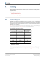
Clocking . . . . . . . . . . . . . . . . . . . . . . . . . . . . . . . . . . . . . . . . . . . . . . . . . . . . . . . . . . 69
A.1
Line Rate Support . . . . . . . . . . . . . . . . . . . . . . . . . . . . . . . . . . . . . . . . . . . . . . . . . . . . . . . . . . . . . 69
A.2
P_CLK Programming . . . . . . . . . . . . . . . . . . . . . . . . . . . . . . . . . . . . . . . . . . . . . . . . . . . . . . . . . . 70
Ordering Information . . . . . . . . . . . . . . . . . . . . . . . . . . . . . . . . . . . . . . . . . . . . . . . . 83
B.1
Ordering Information . . . . . . . . . . . . . . . . . . . . . . . . . . . . . . . . . . . . . . . . . . . . . . . . . . . . . . . . . . 83
B.2
Part Numbering Information . . . . . . . . . . . . . . . . . . . . . . . . . . . . . . . . . . . . . . . . . . . . . . . . . . . . 83
Tundra Semiconductor Corporation
www.tundra.com
Tsi578 Hardware Manual
80B803A_MA002_07
4
Tsi578 Hardware Manual
80B803A_MA002_07
Contents
Tundra Semiconductor Corporation
www.tundra.com
5
About this Document
This section discusses general document information about the Tsi578 Serial RapidIO Switch
Hardware Manual. The following topics are described:
•
“Scope” on page 5
•
“Document Conventions” on page 5
•
“Revision History” on page 7
Scope
The Tsi578 Serial RapidIO Switch Hardware Manual discusses electrical, physical, and board
layout information for the Tsi578. It is intended for hardware engineers who are designing
system interconnect applications with these devices.
Document Conventions
This document uses a variety of conventions to establish consistency and to help you quickly
locate information of interest. These conventions are briefly discussed in the following sections.
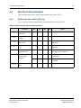
Non-differential Signal Notation
Non-differential signals are either active-low or active-high. An active-low signal has an active
state of logic 0 (or the lower voltage level), and is denoted by a lowercase “b”. An active-high
signal has an active state of logic 1 (or the higher voltage level), and is not denoted by a special
character. The following table illustrates the non-differential signal naming convention.
State
Single-line signal
Multi-line signal
Active low
NAME_b
NAMEn[3]
Active high
NAME
NAME[3]
Tundra Semiconductor Corporation
www.tundra.com
Tsi578 Hardware Manual
80B803A_MA002_07
6
Differential Signal Notation
Differential signals consist of pairs of complement positive and negative signals that are
measured at the same time to determine a signal’s active or inactive state (they are denoted by
“_p” and “_n”, respectively). The following table illustrates the differential signal naming
convention.
State
Single-line signal
Multi-line signal
Inactive
NAME_p = 0
NAME_n = 1
NAME_p[3] = 0
NAME_n[3] =1
Active
NAME_p = 1
NAME_n = 0
NAME_p[3] is 1
NAME_n[3] is 0
Symbols
This symbol indicates a basic design concept or information considered helpful.
Ti
p
This symbol indicates important configuration information or suggestions.
This symbol indicates procedures or operating levels that may result in misuse or
damage to the device.
Tsi578 Serial RapidIO Switch Hardware Manual
80B803A_MA002_07
Tundra Semiconductor Corporation
www.tundra.com
7
Revision History
80B803A_MA002_07, Final, November 2007
This is the production version of the Tsi578 Serial RapidIO Switch Hardware Manual. The key
changes include clarification to the following areas:
•
Information on “P_CLK Programming” on page 70 was added to “Clocking” on page 69.
•
General clarification in “Signals and Package” on page 11, including:
— Any unused signal that is designated a No Connect (N/C) must be left unconnected
— The I2C_SCLK signal description was updated
— The BCE signal description was updated
80B803A_MA002_06, Final, August 2007
This release of the Tsi578 Serial RapidIO Switch Hardware Manual had the following
modifications:
•
A footnote has been added to the recommended terminations in “Signal Grouping” on
page 12.
•
Signals SP_RX_SWAP and SP_TX_SWAP were added to Table 2 on page 12
•
The production versions of the part numbers are now listed in “Ordering Information” on
page 83
80B803A_MA002_05, Final, January 2007
This release of the Tsi578 Serial RapidIO Switch Hardware Manual had the following
modifications:
•
Corrected information in “Power Dissipation” on page 32
Updated information in “Thermal Characteristics” on page 25
80B803A_MA002_04, Final, January 2007
This release of the Tsi578 Serial RapidIO Switch Hardware Manual had the following
modifications:
•
Added information to “Power Sequencing” on page 34
•
The Tstorage (Storage temperature) was changed to a minimum value of -55°C and a
maximum value of 125°C in Table 6 on page 29
Tundra Semiconductor Corporation
www.tundra.com
Tsi578 Hardware Manual
80B803A_MA002_07
8
80B803A_MA002_03, Final, October 2006
This release of the Tsi578 Serial RapidIO Switch Hardware Manual had a number of
modifications. A new “Clocking” on page 69 was been added, as well as power information in
“Power” on page 32.
80B803A_MA002_02, Final, September 2006
This release of the Tsi578 Serial RapidIO Switch Hardware Manual has had a number of
modifications. The electrical and packaging sections have had extensive revisions and the
layout chapter has been added.
Tsi578 Serial RapidIO Switch Hardware Manual
80B803A_MA002_07
Tundra Semiconductor Corporation
www.tundra.com
9
Bibliography
1
RapidIO Interconnect Specification
(Revision 1.3)
This specification explains RapidIO’s logical layer,
common transport layer, and physical layer protocol and
packet formats. It also describes overall inter-operability
requirements for the RapidIO protocol. For more
information, see www.rapidio.org.
2
Enhancements to the RapidIO AC
Specification
This document contains the AC specifications for the
RapidIO physical layer.
ANSI/TIA/EIA-644-1995,
This documents the LVDS electrical characteristics.
3
Electrical Characteristics of Low
Voltage Differential Signaling
(LVDS) Interface Circuits, March
1996.
4
I2C Specification
This specification defines the standard I2C bus
interface, including specifications for all the
enhancements. For more information, see
www.semiconductors.philips.com
document number: 9398 393 40011
5
High-Speed Digital System
Hall,Stephen H.,Garret W. Hall & James A. McCall,
Design
©2000 John
Wiley & Sons inc.
ISBN 0-471-36090-2
6
High-Speed Digital Design
Johnson, Howard, Martin Graham
©1993 Prentice-Hall inc.
ISBN 0-13-395724-1
7
High Performance Printed
Harper, Charles A.
Circuit Boards
©1999 McGraw-Hill
ISBN 0-07-026713-8
8
Transmission Line
Application Note 905
RAPIDESIGNER©
©1996 National Semiconductor Corp.
Lit # 100905-002 & 633201-001
9
High Speed PCB Design
Ritchey, Lee W., James C. Blankenhorn
©1993 SMT Plus Inc., and Ritch Tech
10
Design Guidelines for Electronic
The Institute for Interconnecting and Packaging
Packaging Utilizing High Speed
Electronic Circuits
Techniques
©1999 IPC
Document # IPC-D-317A
Tundra Semiconductor Corporation
www.tundra.com
Tsi578 Hardware Manual
80B803A_MA002_07
10
11
High Speed Signal Propagation
Johnson, Howard, Martin Graham
©2003 Prentice-Hall inc.
ISBN 0-13-084408-X
12
High Speed Digital Design and PCB
Layout
Hanson, Robert J.
1-10 GBps Serial Interconnect
Requirements
Solving High Speed Serial Design Challenges
10GBps Serial Backplanes Using
Virtex-II Pro X
Solving High Speed Serial Design Challenges
15
Designing Controlled-impedance Vias
Thomas Neu, EDN magazine, October 2 2003
16
Computer Circuits Electrical Design,
First Edition,
Ron K. Poon
Tsi578 RapidIO Switch User Manual
Tundra Semiconductor document number:
80B803A_MA001_0x.pdf
13
14
17
Tsi578 Serial RapidIO Switch Hardware Manual
80B803A_MA002_07
©AmeriCom Test & SMT Technology Inc.
©2004Xilinx
©2004Xilinx
Prentice-Hall, Inc., 1995
Tundra Semiconductor Corporation
www.tundra.com
11
1.
Signals and Package
This chapter describes the packaging (mechanical) features for the Tsi578. It includes the
following information:
1.1
•
“Pinlist” on page 11
•
“Signals” on page 11
•
“Package Characteristics” on page 22
•
“Thermal Characteristics” on page 25
Pinlist
Refer to the Tundra website at www.tundra.com for information on the Tsi578 package pinlist
and ballmap.
1.2
Signals
The following conventions are used in the signal description table:
•
Signals with the suffix “_p” are the positive half of a differential pair.
•
Signals with the suffix “_n” are the negative half of a differential pair.
•
Signals with the suffix “_b” are active low.
Signals are classified according to the types defined in Table 1.
Table 1: Signal Types
Pin Type
Definition
I
Input
O
Output
I/O
Input/Output
OD
Open Drain
SRIO
Differential driver/receiver defined by RapidIO
Interconnect Specification (Revision 1.3)
PU
Pulled Up internal to the Tsi578
Tundra Semiconductor Corporation
www.tundra.com
Tsi578 Hardware Manual
80B803A_MA002_07
12
1. Signals and Package
Table 1: Signal Types (Continued)
Pin Type
Definition
PD
Pulled Down internal to the Tsi578
LVTTL
CMOS I/O with LVTTL thresholds
Hyst
Hysteresis
Core Power
Core supply
Core Ground
Ground for core logic
I/O Power
I/O supply
N/C
No connect
These signals must be left unconnected.
1.2.1
Endian Ordering
This document follows the bit-numbering convention adopted by RapidIO Interconnect
Specification (Revision 1.3), where [0:7] is used to represent an 8 bit bus with bit 0 as the
most-significant bit.
1.2.2
Signal Grouping
Table 2 lists the signals by group and their recommended termination.
Table 2: Signal Descriptions and Recommended Termination
Pin Name
Type
Recommended
Terminationa
Description
PORT n - 1x/4x Mode Serial RapidIO
PORT (n+1) - 1x Mode Serial RapidIO
n = 0, 2, 4, 6, 8, 10, 12, 14
SP{n}_TA_p
O, SRIO
Port n Lane A Differential Non-inverting Transmit
Data output (4x mode)
No termination required.
Port n Differential Non-inverting Transmit Data
output (1x mode)
SP{n}_TA_n
O, SRIO
Port n Lane A Differential Inverting Transmit Data
output (4x mode)
No termination required.
Port n Differential Inverting Transmit Data output
(1x mode)
Tsi578 Hardware Manual
80B803A_MA002_07
Tundra Semiconductor Corporation
www.tundra.com
1. Signals and Package
13
Table 2: Signal Descriptions and Recommended Termination
Recommended
Terminationa
Pin Name
Type
Description
SP{n}_TB_p
O, SRIO
Port n Lane B Differential Non-inverting Transmit
Data output (4x mode)
Port n+1 Differential Non-inverting Transmit Data
output (1x mode)
SP{n}_TB_n
O, SRIO
Port n Lane B Differential Inverting Transmit Data
output (4x mode)
Port n+1 Differential Inverting Transmit Data
output (1x mode)
No termination required.
SP{n}_TC_p
O, SRIO
Port n Lane C Differential Non-inverting Transmit
Data output (4x mode)
No termination required.
SP{n}_TC_n
O, SRIO
Port n Lane C Differential Inverting Transmit Data
output (4x mode)
No termination required.
SP{n}_TD_p
O, SRIO
Port n Lane D Differential Non-inverting Transmit
Data output (4x mode)
No termination required.
SP{n}_TD_n
O, SRIO
Port n Lane D Differential Inverting Transmit Data
output (4x mode)
No termination required.
I, SRIO
Port n Lane A Differential Non-inverting Receive
Data input (4x node)
No termination required.
Serial Port n/n+1 Receive
n = 0, 2, 4, 6, 8, 10, 12, 14
SP{n}_RA_p
DC blocking capacitor of
0.1uF in series
Port n Differential Non-inverting Receive Data
input (1x mode)
SP{n}_RA_n
I, SRIO
Port n Lane A Differential Inverting Receive Data
input (4x mode)
DC blocking capacitor of
0.1uF in series
Port n Differential Inverting Receive Data input (1x
mode)
SP{n}_RB_p
I, SRIO
Port n Lane B Differential Non-inverting Receive
Data input (4x mode)
Port n+1 Differential Non-inverting Receive Data
input (1x mode)
DC blocking capacitor of
0.1uF in series
SP{n}_RB_n
I, SRIO
Port n Lane B Differential Inverting Receive Data
input (4x mode)
Port n+1 Differential Inverting Receive Data input
(1x mode)
DC blocking capacitor of
0.1uF in series
SP{n}_RC_p
I, SRIO
Port n Lane C Differential Non-inverting Receive
Data input (4x mode)
DC blocking capacitor of
0.1uF in series
Tundra Semiconductor Corporation
www.tundra.com
Tsi578 Hardware Manual
80B803A_MA002_07
14
1. Signals and Package
Table 2: Signal Descriptions and Recommended Termination
Pin Name
Type
Description
Recommended
Terminationa
SP{n}_RC_n
I, SRIO
Port n Lane C Differential Inverting Receive Data
input (4x mode)
DC blocking capacitor of
0.1uF in series
SP{n}_RD_p
I, SRIO
Port n Lane D Differential Non-inverting Receive
Data input (4x mode)
DC blocking capacitor of
0.1uF in series
SP{n}_RD_n
I, SRIO
Port n Lane D Differential Inverting Receive Data
input (4x mode)
DC blocking capacitor of
0.1uF in series
Used to connect a 190Ω (+/-1%) resistor to VSS
to provide a reference current for the driver and
equalization circuits.
Series resistor of 191Ω
(1%) connected to VSS.
I/O,
LVTTL,
Selects the serial port operating mode for ports n
and n+1
PD
0 - Port n operating in 4x mode (Port n+1 not
available)
Pin must be tied off
according to the required
configuration. Either a 10K
pull up to VDD_IO or a
10K pull-down to VSS_IO.
Serial Port n/n+1 Configuration
n = 0, 2, 4, 6, 8, 10, 12, 14
SP{n}_REXT
SP{n}_MODESEL
1 - Ports n and n+1 operating in 1x mode
Note: Output capability of this pin is only used in
test mode.
Internal pull-down may be
used for logic 0.
Must remain stable for 10 P_CLK cycles after
HW_RST_B is de-asserted in order to be sampled
correctly. Ignored after reset.
SP{n}_PWRDN
I/O,
LVTTL,
PU
Port n Transmit and Receive Power Down control
This signal controls the state of Port n and Port
n+1
The PWRDN controls the state of all four lanes
(A/B/C/D) of SERDES Macro.
0 - Port n Powered Up. Port n+1 controlled by
SP{n+1}_PWRDN.
1 - Port n Powered Down. Port n+1 Powered
Down.
Pin must be tied off
according to the required
configuration. Either a 10K
pull up to VDD_IO or a
10K pull-down to VSS_IO.
Internal pull-up may be
used for logic 1.
Override SP{n}_PWRDN using PWDN_x1 field in
“SRIO MAC x Clock Selection Register” in the
Tsi578 User Manual.
Output capability of this pin is only used in test
mode.
Must remain stable for 10 P_CLK cycles after
HW_RST_B is de-asserted in order to be sampled
correctly. Ignored after reset.
Tsi578 Hardware Manual
80B803A_MA002_07
Tundra Semiconductor Corporation
www.tundra.com
1. Signals and Package
15
Table 2: Signal Descriptions and Recommended Termination
Pin Name
Type
Description
SP{n+1}_PWRDN
I/O,
LVTTL,
Port n+1 Transmit and Receive Power Down
control
This signal controls the state of Port n+1. Note
that Port n+1 is never used when 4x mode is
selected for a Serial Rapid IO MAC, and it must
be powered down.
PU
0 - Port n+1 Powered Up
1 - Port n+1 Powered Down
Recommended
Terminationa
Pin must be tied off
according to the required
configuration. Either a 10K
pull up to VDD_IO or a
10K pull-down to VSS_IO.
Internal pull-up may be
used for logic 1.
Override SP{n+1}_PWRDN using PWDN_x4 field
in “SRIO MAC x Clock Selection Register” in the
Tsi578 User Manual.
Output capability of this pin is only used in test
mode.
Must remain stable for 10 P_CLK cycles after
HW_RST_B is de-asserted in order to be sampled
correctly. Ignored after reset.
Serial Port Speed Select
SP_IO_SPEED[1]
I/O,
LVTTL,
PD
Serial Port Transmit and Receive operating
frequency select, bit 1. When combined with
SP_IO_SPEED[0], this pin selects the default
serial port frequency for all ports.
00 = 1.25Gbit/s;
01 = 2.5Gbit/s (default) ;
10 = 3.125Gbit/s;
Pin must be tied off
according to the required
configuration. Either a 10K
pull-up to VDD_IO or a
10K pull-down to VSS_IO.
Internal pull-down may be
used for logic 0.
11 = illegal
Selects the speed at which the ports operates
when reset is removed. This could be either due
to HARD_RST_b being de-asserted or by the
completion of a self-reset.
This signal must remain stable for 10 P_CLK
cycles after HW_RST_B is de-asserted in order to
be sampled correctly. The signal is ignored after
reset.
The SP_IO_SPEED[1:0] setting is equal to the
SCLK_SEL field inSRIO MAC x Clock Selection
Register in the Tsi578 User Manual.
Output capability of this pin is only used in test
mode.
Tundra Semiconductor Corporation
www.tundra.com
Tsi578 Hardware Manual
80B803A_MA002_07
16
1. Signals and Package
Table 2: Signal Descriptions and Recommended Termination
Pin Name
Type
Description
SP_IO_SPEED[0]
I/O,
LVTTL,
See SP_IO_SPEED[1]
Recommended
Terminationa
Pin must be tied off
according to the required
configuration. Either a 10K
pull-up to VDD_IO or a
10K pull-down to VSS_IO.
PU
Internal pull-up may be
used for logic 1.
Serial Port Lane Ordering Select
SP_RX_SWAP
I, LVTTL,
PD
Configures the order of 4x receive lanes on serial
ports [0,2,4,6,...,14].
0 = A, B, C, D
1 = D, C, B, A
Must remain stable for 10 P_CLK cycles after
HARD_RST_b is de-asserted in order to be
sampled correctly. Ignored after reset.
SP_TX_SWAP
I, LVTTL,
PD
No termination required.
Internal pull-down can be
used for logic 0. Pull up to
VDD_IO through 10K if
external pull-up is desired.
Pull down to VSS_IO
through 10K if external
pull-down is desired.
Configures the order of 4x transmit lanes on serial
ports [0,2,4,6,...,14].
0 = A, B, C, D
1 = D, C, B, A
Must remain stable for 10 P_CLK cycles after
HARD_RST_b is de-asserted in order to be
sampled correctly. Ignored after reset.
No termination required.
Internal pull-down can be
used for logic 0. Pull up to
VDD_IO through 10K if
external pull-up is desired.
Pull down to VSS_IO
through 10K if external
pull-down is desired.
Clock and Reset
P_CLK
S_CLK_p
I
This clock is used for the register bus clock.
CML
The maximum frequency of this input clock is
100 MHz.
I
Differential non-inverting reference clock. The
clock is used for following purposes: SERDES
reference clock, serial port system clock, ISF
clock and test clock. The clock frequency is
defined in the Minimum Clock Frequency
Requirements section.
CML
No termination required.
AC coupling capacitor of
0.1uF required.
The maximum frequency of this input clock is
156.25 MHz.
Tsi578 Hardware Manual
80B803A_MA002_07
Tundra Semiconductor Corporation
www.tundra.com
1. Signals and Package
17
Table 2: Signal Descriptions and Recommended Termination
Pin Name
Type
Description
S_CLK_n
I
Differential inverting reference clock. The clock is
used for following purposes: SerDes reference
clock, serial port system clock, ISF clock and test
clock. The clock frequency is defined in the
Minimum Clock Frequency Requirements section.
CML
Recommended
Terminationa
AC coupling capacitor of
0.1uF required.
The maximum frequency of this input clock is
156.25 MHz.
HARD_RST_b
I
LVTTL,
Hyst,
Schmidt-triggered hard reset. Asynchronous
active low reset for the entire device.
Connect to a power-up
reset source. See “Reset
Requirements” on page 64
for more detail.
PU
The Tsi578 does not contain a voltage detector to
generate internal reset.
O, OD,
Interrupt signal (open drain output)
External pull-up required.
Pull up to VDD_IO through
10K.
Software reset (open drain output): This signal is
asserted when a RapidIO port receives a valid
reset request on a RapidIO link. If self-reset is not
selected, this pin remains asserted until the reset
request is cleared from the status registers. If
self-reset is selected, this pin remains asserted
until the self reset is complete. If the Tsi578 is
reset from the HARD_RST_b pin, this pin is
de-asserted and remains de-asserted after
HARD_RST_b is released.
External pull-up required.
Pull up to VDD_IO through
10K.
Interrupts
INT_b
LVTTL,
2mA
SW_RST_b
O, OD,
LVTTL,
2mA
For more information, refer to “Resets” in the
Tsi578 User’s Manual.
Miscellaneous
Multicast
Tundra Semiconductor Corporation
www.tundra.com
Tsi578 Hardware Manual
80B803A_MA002_07
18
1. Signals and Package
Table 2: Signal Descriptions and Recommended Termination
Pin Name
Type
Description
MCES
I/O,
LVTTL,
PD
Multicast Event Symbol pin.
Recommended
Terminationa
As an input, an edge (rising or falling) will trigger a
Multicast Event Control Symbol will be sent to all
ports;
As an output, this pin will toggle its value every
time an Multicast Event Control Symbol is
received by any port which is enabled for
Multicast even control symbols.
No termination required.
This pin must not be driven
by an external source until
all power supply rails are
stable.
Must remain stable for 10 P_CLK cycles before
and after a transition.
I2C
I2C_SCLK
O, OD,
LVTTL,
PU
I2C clock, up to 100 kHz.
This clock signal must be connected to the clock
of the serial EEPROM on the I2C bus.
8mA
I2C_SD
I/O, OD,
LVTTL,
PU
I2C input and output data bus (bidirectional open
drain)
No termination required.
Internal pull-up may be
used for logic 1. Pull up to
VDD_IO through a
minimum 470 ohms
resistor if higher edge rate
required.
No termination
required.Pull up to
VDD_IO through 10K if if
I2C loading is not required.
8mA
I2C_DISABLE
I, LVTTL,
PD
Disable I2C register loading after reset. When
asserted, the Tsi578 will not attempt to load
register values from I2C.
I2C_MA
I, CMOS,
PU
I2C Multibyte Address.
When driven high, I2C module will expect
multi-byte peripheral addressing; otherwise, when
driven low, single-byte peripheral address is
assumed.
Must remain stable for 10 P_CLK cycles after
HW_RST_b is de-asserted in order to be sampled
correctly. Ignored after reset.
Tsi578 Hardware Manual
80B803A_MA002_07
No termination required.
Internal pull-up may be
used for logic 1. Pull up to
VDD_IO through a
minimum 470 ohms
resistor if higher edge rate
required.
No termination required.
Internal pull-up may be
used for logic 1.
Pull up to VDD_IO through
10K resistor if external
pull-up is desired. Pull
down to VSS_IO to
change the logic state.
Tundra Semiconductor Corporation
www.tundra.com
1. Signals and Package
19
Table 2: Signal Descriptions and Recommended Termination
Pin Name
Type
Description
I2C_SA[1,0]
I, CMOS,
PU
I2C Slave Address pins.
The values on these two pins represent the
values for the lower 2 bits of the 7-bit address of
Tsi578 when acting as an I2C slave.
The values at these pins can be overridden by
software after reset.
I2C_SEL
I, CMOS,
PU
I2C Pin Select. Together with the I2C_SA[1,0]
pins, Tsi578 will determine the lower 2 bits of the
7-bit address of the EEPROM address it boots
from.
When asserted, the I2C_SA[1,0] values will also
be used as the lower 2 bits of the EEPROM
address.
When de-asserted, the I2C_SA[1,0] pins will be
ignored and the lower 2 bits of the EEPROM
address are default to 00.
Recommended
Terminationa
No termination required.
Internal pull-up may be
used for logic 1.
Pull up to VDD_IO through
10K resistor if external
pull-up is desired. Pull
down to VSS_IO to
change the logic state.
No termination required.
Internal pull-up may be
used for logic 1.
Pull up to VDD_IO through
10K resistor if external
pull-up is desired. Pull
down to VSS_IO to
change the logic state.
The values of the lower 2 bits of the EEPROM
address can be over-ridden by software after
reset.
JTAG TAP Controller
TCK
I, LVTTL,
PD
IEEE 1149.1 Test Access Port
Clock input
Pull up to VDD_IO through
10K if not used.
TDI
I, LVTTL,
PU
IEEE 1149.1 Test Access Port
Serial Data Input
Pull up to VDD_IO through
10K if not used or if higher
edge rate is required.
TDO
O,
LVTTL,
IEEE 1149.1 Test Access Port
Serial Data Output
No connect if JTAG is not
used. Pull up to VDD_IO
through 10K if used.
IEEE 1149.1 Test Access Port
Test Mode Select
Pull up to VDD_IO through
10K if not used.
2mA
TMS
I, LVTTL,
PU
Tundra Semiconductor Corporation
www.tundra.com
Tsi578 Hardware Manual
80B803A_MA002_07
20
1. Signals and Package
Table 2: Signal Descriptions and Recommended Termination
Recommended
Terminationa
Pin Name
Type
Description
TRST_b
I, LVTTL,
PU
IEEE 1149.1 Test Access Port TAP Reset Input
This input must be asserted during the assertion
of HARD-RST_b. Afterwards, it may be left in
either state.
Tie to VSS_IO through a
10K resistor if not used.
Combine the HARD_RST_b and TRST_b signals
with an AND gate and use the output to drive the
TRST_b pin.
BCE
I, LVTTL,
PU
Boundary Scan compatibility enabled pin. This
input is used to aid 1149.6 testing.
This signal also enables system level diagnostic
capability using features built into the SerDes. For
more information on this functionality, refer to the
Serial RapidIO Signal Analyzer documentation
available on the Tundra extranet.
This signal must be tied to VDD_IO during normal
operation of the device, and during JTAG
accesses of the device registers
This signal should have
the capability to be
pulled-up or pulled-low.
• The default setting is to
be pulled-up.
• Pulling the signal low
enables the signal
analyzer functionality on
the SerDes
A 10K resistor to VDD_IO
should be used.
Power Supplies
Port n/n+1
n = 0, 2, 4, 6, 8, 10, 12, 14
SP{n}_AVDD
-
REF_AVDD
-
Port n and n+1: 3.3V supply for bias generator
circuitry. This is required to be a low-noise supply.
Analog 1.2V for Reference Clock (S_CLK_p/n).
Clock distribution network power supply.
Refer to “Decoupling
Requirements” on
page 57.
Refer to “Decoupling
Requirements” on
page 57.
Common Supply
VDD_IO
-
Common 3.3V supply for CMOS I/O
Refer to “Decoupling
Requirements” on
page 57.
VSS_IO
-
Common ground supply for I/Os
Refer to “Decoupling
Requirements” on
page 57.
Tsi578 Hardware Manual
80B803A_MA002_07
Tundra Semiconductor Corporation
www.tundra.com
1. Signals and Package
21
Table 2: Signal Descriptions and Recommended Termination
Recommended
Terminationa
Pin Name
Type
Description
VSS
-
Common ground supply for digital logic
Refer to “Decoupling
Requirements” on
page 57.
VDD
-
Common 1.2V supply for digital logic
Refer to “Decoupling
Requirements” on
page 57.
SP_VDD
-
1.2V supply for CDR, Tx/Rx, and digital logic for
all RapidIO ports
Refer to “Decoupling
Requirements” on
page 57.
a. Signals for unused serial ports do not require termination and can be left as N/Cs.
Tundra Semiconductor Corporation
www.tundra.com
Tsi578 Hardware Manual
80B803A_MA002_07
22
1.3
1. Signals and Package
Package Characteristics
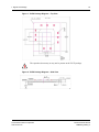
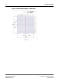
The Tsi578’s package characteristics are summarized in the following table. Figure 1 and
Figure 2 illustrates the Top and Side views of the Tsi578 package. Figure 3 represents the
Bottom view of the device.
Table 3: Tsi578 Package Characteristics
Feature
Description
Package Type
Flip-Chip Ball Grid Array (FCBGA)
Ball count
675-ball
Package Body Size
27 mm x 27 mm
JEDEC Specification
95-1 Section 14
Pitch
1.00 mm
Ball pad size
500 um
Soldermask opening
400 um
Moisture Sensitivity Level
4
Tsi578 Hardware Manual
80B803A_MA002_07
Tundra Semiconductor Corporation
www.tundra.com
1. Signals and Package
23
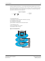
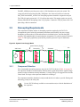
Figure 1: Tsi578 Package Diagram — Top View
The capacitors shown may or may not be present on the Tsi578 package.
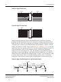
Figure 2: Tsi578 Package Diagram — Side View
Tundra Semiconductor Corporation
www.tundra.com
Tsi578 Hardware Manual
80B803A_MA002_07
24
1. Signals and Package
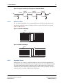
Figure 3: Tsi578 Package Diagram — Bottom View
Tsi578 Hardware Manual
80B803A_MA002_07
Tundra Semiconductor Corporation
www.tundra.com
1. Signals and Package
1.4
25
Thermal Characteristics
Heat generated by the packaged IC has to be removed from the package to ensure that the IC is
maintained within its functional and maximum design temperature limits. If heat buildup
becomes excessive, the IC temperature may exceed the temperature limits. A consequence of
this is that the IC may fail to meet the performance specifications and the reliability objectives
may be affected.
Failure mechanisms and failure rate of a device have an exponential dependence of the IC
operating temperatures. Thus, the control of the package temperature, and by extension the
Junction Temperature, is essential to ensure product reliability. The Tsi578 is specified safe for
operation when the Junction Temperature is within the recommended limits.
Table 4 shows the simulated Theta jb and Theta jc thermal characteristics of the Tsi578 FCBGA
package.
Table 4: Thermal Characteristics of Tsi578
1.4.1
Interface
Result
Theta jb (junction to board)
11.7 °C/watt
Theta jc (junction to case)
0.08 °C/watt
Junction-to-Ambient Thermal Characteristics (Theta ja)
Table 5 shows the simulated Theta ja thermal characteristic of the Tsi578 FCBGA package.The
results in Table 5 are based on a JEDEC Thermal Test Board configuration (JESD51-9) and do
not factor in system level characteristics. As such, these values are for reference only.
The Theta ja thermal resistance characteristics of a package depend on multiple
system level variables.
Table 5: Simulated Junction to Ambient Characteristics
Theta ja at specified airflow (no Heat Sink)
Package
0 m/s
1 m/s
2 m/s
Tsi578 FCBGA
14.6 C/watt
13.6 °C/watt
12.9 °C/watt
Tundra Semiconductor Corporation
www.tundra.com
Tsi578 Hardware Manual
80B803A_MA002_07
26
1.4.1.1
1. Signals and Package
System-level Characteristics
In an application, the following system-level characteristics and environmental issues must be
taken into account:
•
Package mounting (vertical / horizontal)
•
System airflow conditions (laminar / turbulent)
•
Heat sink design and thermal characteristics (see “Heatsink Requirement and Analysis” on
page 26)
•
Heat sink attachment method (see “Heatsink Requirement and Analysis” on page 26)
•
PWB size, layer count and conductor thickness
•
Influence of the heat dissipating components assembled on the PWB (neighboring effects)
Example on Thermal Data Usage
Based on the ThetaJA data and specified conditions, the following formula can be used to derive
the junction temperature (Tj) of the Tsi578 with a 0m/s airflow:
•
Tj = θJA * P + Tamb.
Where: Tj is Junction Temperature, P is the Power consumption, Tamb is the Ambient
Temperature
Assuming a power consumption (P) of 3.5 W and an ambient temperature (Tamb) of 70°C, the
resulting junction temperature (Tj) would be 121.1°C.
1.4.2
Heatsink Requirement and Analysis
The Tsi578 is packaged in a Flip-Chip Ball Grid Array (FCBGA). With this package
technology, the silicon die is exposed and serves as the interface between package and heatsink.
Where a heatsink is required to maintain junction temperatures at or below specified maximum
values, it is important that attachment techniques and thermal requirements be critically
analyzed to ensure reliability of this interface. Factors to be considered include: surface
preparations, selection of thermal interface materials, curing process, shock and vibration
requirements, and thermal expansion coefficients, among others. Each design should be
individually analyzed to ensure that a reliable thermal solution is achieved.
Both mechanical and adhesive techniques are available for heatsink attachment.
Tundra makes no recommendations as to the reliability or effectiveness of either
approach. The designer must critically analyze heatsink requirements, selection
criteria, and attachment techniques.
Tsi578 Hardware Manual
80B803A_MA002_07
Tundra Semiconductor Corporation
www.tundra.com
1. Signals and Package
1.4.2.1
27
Heatsink Attachment
Both mechanical and adhesive techniques are available for heatsink attachment.
Both mechanical and adhesive techniques are available for heatsink attachment.
Tundra makes no recommendations as to the reliability or effectiveness of either
approach. The designer must critically analyze heatsink requirements, selection
criteria, and attachment techniques.
For heatsink attachment methods that induce a compressive load to the FCBGA package, the
maximum force that can be applied to the package should be limited to 5 gm / BGA ball
(provided that the board is supported to prevent any flexing or bowing). The maximum force for
the Tsi578 package is 3.38 Kg.
Tundra Semiconductor Corporation
www.tundra.com
Tsi578 Hardware Manual
80B803A_MA002_07
28
Tsi578 Hardware Manual
80B803A_MA002_07
1. Signals and Package
Tundra Semiconductor Corporation
www.tundra.com
29
2.
Electrical Characteristics
This chapter provides the electrical characteristics for the Tsi578. It includes the following
information:
2.1
•
“Absolute Maximum Ratings” on page 29
•
“Recommended Operating Conditions” on page 30
•
“Power” on page 32
Absolute Maximum Ratings
Operating the device beyond the operating conditions is not recommended. Stressing the Tsi578
beyond the Absolute Maximum Rating can cause permanent damage.
Table 6 lists the absolute maximum ratings.
Table 6: Absolute Maximum Ratings
Symbol
Parameter
Min
Max
Unit
Tstorage
Storage Temperature
-55
125
°C
VDD_IO
3.3 V DC Supply Voltage
-0.5
4.6
V
3.3 V Analog Supply Voltage
-0.5
4.6
V
1.2 V DC Supply Voltage
-0.3
1.7
V
VI_SP{n}-R{A-D}_{p,n}
SERDES Port Receiver Input Voltage
-0.3
3
V
VO_SP{n}-T{A-D}_{p,n}
SERDES Port VM Transmitter Output Voltage
-0.3
3
V
SP{n}_AVDD
VDD, SP_VDD,
REF_AVDD
SP{n}_AVDD
Transient di/dt
-
0.0917
A/nS
SP_AVDD
Transient di/dt
-
0.136
A/nS
Tundra Semiconductor Corporation
www.tundra.com
Tsi578 Hardware Manual
80B803A_MA002_07
30
2. Electrical Characteristics
Table 6: Absolute Maximum Ratings
2.2
Symbol
Parameter
Min
Max
Unit
VO_LVTTL
LVTTL Output or I/O Voltage
-0.5
VDD_IO +0.5
V
VESD_HBM
Maximum ESD Voltage Discharge Tolerance
for Human Body Model (HBM). [Test
Conditions per JEDEC standard JESD22-A114-B]
-
2000
V
VESD_CDM
Maximum ESD Voltage Discharge Tolerance
for Charged Device Model (CDM). Test
Conditions per JEDEC standard JESD22-C101-A
-
500
V
Recommended Operating Conditions
Table 7 lists the recommended operating conditions.the current values provided are maximum
Continued exposure of Tundra's devices to the maximum limits of the specified
junction temperature could affect the device reliability. Subjecting the devices to
temperatures beyond the maximum/minimum limits could result in a permanent
failure of the device.
Table 7: Recommended Operating Conditions
Symbol
Min
Max
Unit
Junction temperature
-40
125°
°C
3.3 V DC Supply Voltage
2.97
3.63
V
SP{n}_AVDD
3.3 V Analog Supply Voltage
2.97
3.63
V
VDD,SP_VDD,
REF_AVDD
1.2 V DC Supply Voltage
1.14
1.29
V
IVDD_IO
3.3 V IO Supply Currenta
-
15
mA
ISP_VDD
SerDes Digital Supply Currenta
-
716
mA
ISP_AVDD
3.3 V SerDes Supply Currenta
-
480
mA
1.2 V Core Supply Currenta
-
3300
mA
1.2 V Ref Clock Supply Current
-
12.5
mA
Tj
VDD_IO
IVDD
IREF_AVDD
Tsi578 Hardware Manual
80B803A_MA002_07
Parameter
Tundra Semiconductor Corporation
www.tundra.com
2. Electrical Characteristics
31
Table 7: Recommended Operating Conditions
Symbol
Parameter
Min
Max
Unit
Vripple1
Power Supply ripple for Voltage Supplies:
SP_VDD, VDD and VDD_IO
-
100
mVpp
Vripple2
Power Supply ripple for Voltage Supplies:
SP{n}_AVDD, REF_AVDD
-
50
mVpp
External reference resistor current
-
10
uA
IREXT
a. The current values provided are maximum values and dependent on device configuration, such as port
usage, traffic, etc.
Tundra Semiconductor Corporation
www.tundra.com
Tsi578 Hardware Manual
80B803A_MA002_07
32
2. Electrical Characteristics
2.3
Power
The following sections describe the Tsi578’s power dissipation and power sequencing.
2.3.1
Power Dissipation
The power dissipation values provided are dependent on device configuration. The line rate,
port configuration, traffic all impact the Tsi578’s power consumption.
The following table shows the power in both 1x and 4x modes..
Table 8: Measured Power, 1x Mode, 16 Links in Operation
Line Rate
1.25 GBaud
2.5 GBaud
3.125 GBaud
Notes
VDD_CORE
1.07
1.74
2.10
2,9
SP_VDD
0.73
0.75
0.91
3
SPn_AVDD
1.42
1.59
1.83
4
VDD_IO
0.01
0.01
0.01
5
Total Measured Power
Consumption (W)
3.23
4.09
4.84
1,6,7,8
Power Reduction per
Unused Odd Port (W)
0.06
0.10
0.13
10
Power Reduction per
Unused Even Port (W)
0.32
0.37
0.43
11
Notes
1.
Voltage, temperature and process are all nominal
2.
VDD_CORE supplies the ISF and other internal digital logic
3.
SP_VDD supplies the digital portion of the SRIO SerDes
4.
SPn_AVDD supplies the analog portion of the SRIO SerDes
5.
VDD_IO supplies power for all non-SRIO I/O
6.
Total power is independent of SRIO distance travelled due to Voltage Mode Driver
technology used for SRIO I/O
7.
Slight power variations must expected across different applications
8.
Power is provided for fully utilized SRIO lanes
9.
Core power reduces by approximately 10% under light traffic conditions
Tsi578 Hardware Manual
80B803A_MA002_07
Tundra Semiconductor Corporation
www.tundra.com
2. Electrical Characteristics
33
10. The corresponding even port is powered up and fully utilized
11. The corresponding odd port is already powered down. This number represents additional
power reduction which is gained by powering down the even port
The following table represents the measured power in 4x mode.
Table 9: Measured Power, 4x Mode, Eight Links in Operation
Line Rate
1.25GBaud
2.5GBaud
3.125GBaud
Notes
VDD_CORE
1.03
1.65
1.92
2,9
SP_VDD
0.79
0.85
1.06
3
SPn_AVDD
1.49
1.84
2.13
4
VDD_IO
0.01
0.01
0.01
5
Total Measured Power
Consumption (W)
3.32
4.34
5.11
1,6,7, 8
Power Reduction per
Unused Port (W)
0.37
0.50
0.60
10
Notes
1.
Voltage, temperature and process are all nominal
2.
VDD_CORE supplies the ISF and other internal digital logic
3.
SP_VDD supplies the digital portion of the SRIO SerDes
4.
SPn_AVDD supplies the analog portion of the SRIO SerDes
5.
VDD_IO supplies power for all non-SRIO I/O
6.
Total power is independent of SRIO distance travelled due to Voltage Mode Driver
technology used for SRIO I/O
7.
Slight power variations must expected across different applications
8.
Power is provided for fully utilized SRIO lanes
9.
Core power reduces by approximately 10% under light traffic conditions
10. Link pair refers to link groups 0/1, 2/3, etc. The odd numbered ports in the link pairs are
powered down.
Tundra Semiconductor Corporation
www.tundra.com
Tsi578 Hardware Manual
80B803A_MA002_07
34
2.3.2
2. Electrical Characteristics
Power Sequencing
The Tsi578 must have the supplies powered-up in the following order:
•
VDD (1.2 V) must be powered up first
•
SP_VDD (1.2 V) and REF_AVDD (1.2 V) should power up at approximately the same
time as VDD
•
Delays between the powering up of VDD, SP_VDD, and REF_AVDD are acceptable.
•
No more than 50ms after VDD is at a valid level, VDD_IO (3.3 V) should be powered up to
a valid level
•
VDD_IO (3.3V) must not power up before VDD (1.2 V)
•
SPn_AVDD (3.3V) should power up at approximately the same time as VDD_IO
•
Delays between powering up VDD_IO and SPn_AVDD are acceptable
•
SPn_AVDD must not power up before SP_VDD
It is recommended that there not be more than 50ms between ramping of the 1.2 V
and 3.3 V supplies. The power supply ramp rates must be kept between 10 V/s and
1x10E6 V/s to minimize power current spikes during power up.
If it is necessary to sequence the power supplies in a different order than that recommended
above, the following precautions must be taken:
2.3.2.1
•
Any power-up option pins must be current limited with 10 K ohms to VDD_IO or VSS_IO
as required to set the desired logic level.
•
Power-up option pins that are controlled by a logic device must not be driven until all
power supply rails to the Tsi578 are stable.
Power-down
Power down is the reverse sequence of power up:
•
VDD_IO (3.3V) and SP{n}_AVDD
•
VDD (1.2V), SP_VDD and REF_AVDD power-down at the same time, or all rails falling
simultaneously.
Tsi578 Hardware Manual
80B803A_MA002_07
Tundra Semiconductor Corporation
www.tundra.com
2. Electrical Characteristics
2.4
35
Electrical Characteristics
This section describes the AC and DC signal characteristics for the Tsi578.
2.4.1
SerDes Receiver (SP{n}_RD_p/n)
Table 10 lists the electrical characteristics for the SerDes Receiver in the Tsi578.
Table 10: SerDes Receiver Electrical Characteristics
Symbol
Parameter
Min
Typ
Max
Unit
Notes
ZDI
RX Differential Input
impedance
90
100
110
Ohm
-
VDIFFI
RX Differential Input
Voltage
170
-
1600
mV
-
LCR
RX Common Mode
Return Loss
-
-
6
dB
Over a range 100MHz to 0.8* Baud
Frequency
LDR
RX Differential Return
Loss
-
-
10
dB
Over a range 100MHz to 0.8* Baud
Frequency
VLOS
RX Loss of Input
Differential Level
55
-
-
mV
Port Receiver Input level below which
Low Signal input is detected
-
-
24
ns
Between channels in a given x4 port @
1.25/2.5Gb/s
-
-
22
ns
Between channels in a given x4 port @
3.125Gb/s
-
-
160
ps
Between 20% and 80% levels
TRX_ch_skew
RTR,RTF
RX Channel to
Channel Skew
Tolerance
RX Input Rise/Fall
times
Tundra Semiconductor Corporation
www.tundra.com
Tsi578 Hardware Manual
80B803A_MA002_07
36
2. Electrical Characteristics
2.4.2
SerDes Transmitter (SP{n}_TD_p/n)
Table lists the electrical characteristics for the SerDes transmitter in the Tsi578.
Table 11: SerDes Transmitter Electrical Characteristics
Symbol
Parameter
Min
Typ
Max
Unit
Notes
ZSEO
TX Single-Ended
Output impedance
45
50
55
Ohm
-
ZDO
TX Differential Output
Impedance
90
100
110
Ohm
-
VSW
TX Output Voltage
Swing (Single-ended)
425
600
mVp
-p
VSW (in mV) = ZSEO/2 x Inom x
RIdr/Inom, where Ridr/Inom is the Idr to
Inom ratio.
VDIFFO
TX Differential Output
Voltage Amplitude
-
2*VSW
mVp
-p
-
VOL
TX Output Low-level
Voltage
-
1.2 VSW
V
-
VOH
TX Output High-level
Voltage
-
1.2
V
-
VTCM
TX common-mode
Voltage
-
1.2 VSW/2
V
-
LDR1
TX Differential Return
Loss
-
-
10
dB
For (Baud
Frequency)/10<Freq(f)<625MHz and
LDR2
TX Differential Return
Loss
-
-
10 +
|10log(f
/625M
Hz)|
dB
For 625MHz<=Freq(f)<= Baud
Frequency
TTX_skew
TX Differential signal
skew
-
-
15
ps
Skew between _p and _n signals on a
give Serial channel
TTR,TTF
TX Output Rise/Fall
times
80
-
110
ps
Between 20% and 80% levels
Tsi578 Hardware Manual
80B803A_MA002_07
Tundra Semiconductor Corporation
www.tundra.com
2. Electrical Characteristics
2.4.3
37
Reference Clock, S_CLK_p/n
Table 12 lists the electrical characteristics for the differential SerDes Reference clock input
(S_CLK_p/n) in the Tsi578.
Table 12: Reference Clock (S_CLK_p/n) Electrical Characteristics
Symbol
Parameter
VSW
Input voltage
swing
VDIFF
Differential input
voltage swing
VCM
Differential Input
Common Mode
Range
Min
Typ
Max
Unit
0.1
0.5
1
V
VDIFF = VSW * 2
Notes
V
175
-
2000
mV
The S_CLK_p/n must be AC
coupled.
((S_CLK_p +
S_CLK_n)/2)
Fin
Input Clock
Frequency
156.25
-
156.25
MHz
FS_CLK_P/N
Ref Clock
Frequency
Stability
-100
-
+100
ppm
Fin_DC
Ref Clock Duty
Cycle
40
50
60
%
Tskew
Ref Clock Skew
-
-
0.32
ns
TR_SCLK,
TF_SCLK
S_CLK_p/n Input
Rise/Fall Time
-
-
1
ns
JCLK-REF
Total Phase Jitter,
rms
-
-
3
psrms
Zin
Input Impedance
80
100
114
ohms
PPM with respect to 156.25 MHz.
Between _p and _n inputs.
See Belowa
a. Total Permissible Phase Jitter on the Reference Clock is 3 ps rms. This value is specified with assumption that the
measurement is done with a 20 G Samples/s scope with more than 1 million samples taken. The zero-crossing times of
each rising edges are recorded and an average Reference Clock is calculated. This average period may be subtracted
from each sequential, instantaneous period to find the difference between each reference clock rising edge and the
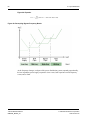
ideal placement to produce the Phase Jitter Sequence. The PSD of the phase jitter is calculated and integrated after
being weighted with the transfer function shown in Figure 4. The square root of the resulting integral is the rms Total
Phase Jitter.
Tundra Semiconductor Corporation
www.tundra.com
Tsi578 Hardware Manual
80B803A_MA002_07
38
2. Electrical Characteristics
Figure 4: Weighing function for RMS Phase Jitter Calculation
2.4.4
LVTTL I/O and Open Drain Signals
Table 13 lists the electrical characteristics for the 3.3 V digital LVTTL Interface pins on the
Tsi578.
Table 13: LVTTL I/O and Open Drain Electrical Characteristics
Symbol
Parameter
Min
Typ
Max
Unit
Notes
0.8
V
All inputs and I/Os of LVTTL type
V
All inputs and I/Os of LVTTL type
VIL
LVTTL Input Low
Voltage
-
-
VIH
LVTTL Input High
Voltage
2.0
-
IIL
LVTTL Input Low
Current
-
-
10
uA
All non-PU inputs and I/Os of LVTTL
type
IIH
LVTTL Input High
Current
-
-
-10
uA
All non-PD inputs and I/Os of LVTTL
type
IOZL_PU, IIL_PU
LVTTL Input Low/
Output Tristate Current
5
-
100
uA
All PU inputs and I/Os of LVTTL type
for voltages from 0 to VDD_IO on the
pin.
IOZH_PD,
IIH_PD
LVTTL Input High/
Output Tristate Current
-5
-
-100
uA
All PD inputs and I/Os of LVTTL type
for voltages from 0 to VDD_IO on the
pin.
LVTTL Output Low
Voltage
-
-
0.4
V
IOL=2mA for INT_b, SW_RST_b,
and TDO pins
VOL
IOL=8mA for I2C_CLK and I2C_SD
pins
VOH
LVTTL Output Low
Voltage
Tsi578 Hardware Manual
80B803A_MA002_07
VDD_IO
-0.5
-
-
V
IOH=2mA for INT_b, SW_RST_b,
and TDO pins
Tundra Semiconductor Corporation
www.tundra.com
2. Electrical Characteristics
39
Table 13: LVTTL I/O and Open Drain Electrical Characteristics
Symbol
Parameter
Min
Typ
Max
Unit
Notes
0.9V Max with a maximum energy of
0.75 V-ns
VOVERSHOOT
Dynamic Overshoot
-
-
0.9
V
VHyst
LVTTL Input
Hysteresis Voltage
-
200
-
mV
All Hyst inputs and I/Os of LVTTL
type
CPad
LVTTL Pad
Capacitance
-
-
10
pF
All pads of LVTTL type
TcfgpS
Configuration Pin
Setup Time
100
-
-
ns
For all Configuration pins (except
SP{n}_MODESEL with respect to
HARD_RST_b rising edge
TcfgpH
Configuration Pin Hold
Time
100
-
-
ns
For all Configuration pins (except
SP{n}_MODESEL) with respect to
HARD_RST_b rising edge
Tsp_modeselS
SP{n}_MODESEL
Setup Time
5
-
-
ns
with respect to rising edge of
P_CLK. SP{n}_MODESEL pins are
sampled on every rising edge of
P_CLK.
Tsp_modeseH
SP{n}_MODESEL
Hold Time
5
-
-
ns
with respect to rising edge of
P_CLK. SP{n}_MODESEL pins are
sampled on every rising edge of
P_CLK.
TISOV1
INT_b/SW_RST_b
Output Valid Delay
from rising edge of
P_CLK
-
-
15
ns
Measured between 50% points on
both signals. Output Valid delay is
guaranteed by design.
TISOF1
INT_b/SW_RST_b
Output Float Delay
from rising edge of
P_CLK
-
-
15
ns
A float condition occurs when the
output current becomes less than
ILO, where ILO is 2 x IOZ. Float delay
guaranteed by design.
Fin_P_CLK
Input Clock Frequency
100
-
100
MHz
-
Fin_STAB
P_CLK Input Clock
Frequency Stability
-100
-
+100
ppm
-
Fin_PCLK_DC
P_CLK Input Clock
Duty Cycle
40
50
60
%
-
JPCLK
P_CLK Input Jitter
-
-
300
pspp
-
P_CLK Input Rise/Fall
Time
-
-
2.5
ns
-
TR_PCLK,
TF_PCLK
Tundra Semiconductor Corporation
www.tundra.com
Tsi578 Hardware Manual
80B803A_MA002_07
40
2. Electrical Characteristics
Table 13: LVTTL I/O and Open Drain Electrical Characteristics
Symbol
fMCES
Parameter
MCES pin frequency
Min
Typ
Max
Unit
Notes
-
-
1
MHz
both as input and output
R pull-up
Resistor pull-up
82K
-
260K
ohms
@Vil=0.8V
R pull-down
Resistor pull-down
28K
-
54K
ohms
@Vih=2.0V
Tsi578 Hardware Manual
80B803A_MA002_07
Tundra Semiconductor Corporation
www.tundra.com
2. Electrical Characteristics
2.4.5
41
I2C Interface
Table 14 lists the AC specifications for Tsi578’s I2C Interface. The I2C interfaces includes balls:
I2C_SCLK, I2C_SD, I2C_DISABLE, I2C_MA, I2C_SEL, I2C_SA[1:0] and I2C_SEL.
Table 14: AC Specifications for I2C Interface
Symbol
Parameter
Min
Max
Units
Notes
0
100
kHz
-
FSCL
I2C_SD/I2C_SCLK Clock Frequency
TBUF
Bus Free Time Between STOP and START Condition
4.7
-
μs
1
TLOW
I2C_SD/I2C_SCLK Clock Low Time
4.7
-
μs
1
THIGH
I2C_SD/I2C_SCLK Clock High Time
4
-
μs
1
THDSTA
Hold Time (repeated) START condition
4
-
μs
1,2
TSUSTA
Setup Time for a Repeated START condition
4.7
-
μs
1
THDDAT
Data Hold Time
0
3.45
μs
1
TSUDAT
Data Setup Time
250
-
ns
1
TSR
Rise Time for I2C_xxx (all I2C signals)
-
1000
ns
1
TSF
Fall Time for I2C_xxx (all I2C signals)
-
300
ns
1
Setup Time for STOP Condition
4
-
μs
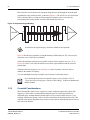
1
TSUSTOP
Notes:
1.
See Figure 5, I2C Interface Signal Timings
2.
After this period, the first clock pulse is generated
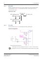
Figure 5: I2C Interface Signal Timings
SDA
TBUF
TLOW
TSR
TSF
THDSTA
TSP
SCL
THDSTA
Stop
Start
Tundra Semiconductor Corporation
www.tundra.com
THDDAT
THIGH TSUDAT TSUSTA
Repeated
Start
TSUSTO
Stop
Tsi578 Hardware Manual
80B803A_MA002_07
42
2. Electrical Characteristics
2.4.6
Boundary Scan Test Interface Timing
Table 15 lists the test signal timings for Tsi578.
Table 15: Boundary Scan Test Signal Timings
Symbol
Parameter
Min
Max
Units
TBSF
TCK Frequency
0
25
MHz
TBSCH
TCK High Time
50
-
ns
Notes
• Measured at 1.5V
• Note test
TBSCL
TCK Low Time
50
-
ns
• Measured at 1.5V
• Note test
TBSCR
TCK Rise Time
-
25
ns
• 0.8V to 2.0V
• Note test
TBSCF
TCK Fall Time
-
25
ns
• 2.0V to 0.8V
• Note test
TBSIS1
Input Setup to TCK
10
-
ns
-
TBSIH1
Input Hold from TCK
10
-
ns
-
TBSOV1
TDO Output Valid Delay from falling edge
of TCK.a
-
15
ns
-
TOF1
TDO Output Float Delay from falling edge
of TCK
-
15
ns
-
TBSTRST1
TRST_B release before HARD_RST_b
release
-
10
ns
TBSTRST2
TRST_B release before TMS or TDI
activity
1
-
ns
TRST_b must become
asserted while
HARD_RST_b is asserted
during device power-up
-
a. Outputs precharged to VDD.
Tsi578 Hardware Manual
80B803A_MA002_07
Tundra Semiconductor Corporation
www.tundra.com
3. Layout Guidelines
3.
43
Layout Guidelines
This chapter describes the layout guidelines for the Tsi578. It includes the following
information:
3.1
•
“Impedance Requirements” on page 43
•
“Tracking Topologies” on page 44
•
“Power Distribution” on page 56
•
“Decoupling Requirements” on page 57
•
“Clocking and Reset” on page 61
•
“Modeling and Simulation” on page 65
•
“Testing and Debugging Considerations” on page 66
•
“Reflow Profile” on page 68
Overview
The successful implementation of a Tsi578 in a board design is dependent on properly routing
the Serial RapidIO signals and maintaining good signal integrity with a resultant low bit error
rate. The sections that follow contain information for the user on principals that will maximize
the signal quality of the links.
Since every situation is different, Tundra urges the designer to model and simulate their board
layout and verify that the layout topologies chosen will provide the performance required of the
product.
3.2
Impedance Requirements
The impedance requirement of the Serial RapidIO interface is 100 ohms differential.
Tundra Semiconductor Corporation
www.tundra.com
Tsi578 Hardware Manual
80B803A_MA002_07
44
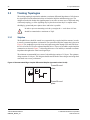
3.3
3. Layout Guidelines
Tracking Topologies
The tracking topologies required to maintain a consistent differential impedance of 100 ohms to
the signal placed on the transmission line are limited to Stripline and Microstrip types. The
designer must decide whether the signalling must be moved to an outer layer of the board using
a Microstrip topology, or if the signalling may be placed on an inner layer as stripline where
shielding by ground and power planes above and below is possible.
In order to prevent consuming received eye margin, the =/- track skew of a lane
should be constrained to a maximum of 15pS.
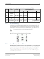
3.3.1
Stripline
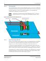
The RapidIO buses should be routed in a symmetrical edge-coupled stripline structure in order
to ensure a constant impedance environment. The symmetrical stripline construction is shown in
Figure 6. This method also provides clean and equal return paths through VSS and VDD from
the I/O cell of the Tsi578 to the adjacent RapidIO device. The use of broadside coupled stripline
construction as shown in Figure 7 is discouraged because of its inability to maintain a constant
impedance throughout the entire board signal layer.
The minimum recommended layer count of a board design consists of 12 layers. The optimum
design consists of 16 layers. The designer should consider both of these designs and weigh their
associated costs versus performance.
Figure 6: Recommended Edge Coupled Differential Stripline (symmetric when h1=h2)
t h1
h2
Power/Ground
plane
W
S
Power/Ground
plane
Tsi578 Hardware Manual
80B803A_MA002_07
Tundra Semiconductor Corporation
www.tundra.com
3. Layout Guidelines
45
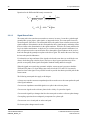
Equations for Stripline and Differential Stripline Impedance (in Ohms):
Zo =
Zdiff
60
ε
r
⎛ 1 . 9 (2 ( h 1 + h 2 ) + t ) ⎞
⎟⎟
× ln ⎜⎜
(
)
0
.
67
π
0
.
8
w
+
t
⎝
⎠
s
⎡
⎤
⎛
− 2 .9 ⎢
⎥
⎣ h1+ h 2 ⎦
= 2 × Zo ⎜ 1 − 0 . 374 e
⎜
⎝
⎞
⎟
⎟
⎠
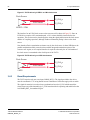
The broadside coupled stripline construction is not recommended for use with RapidIO because
of the manufacturing variations in layer spacings. These variations will cause impedance
mismatch artifacts in the signal waveforms and will degrade the performance of the link.
Figure 7: Not Recommended Broadside Coupled or Dual Stripline Construction
w
t
b
Signal Layer
h
Dielectric
c
Signal Layer
b
3.3.1.1
Microstrip
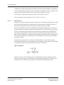
When it is necessary to place the differential signal pairs on the outer surfaces of the board, the
differential microstrip construction is used. Figure 8 shows the construction of the microstrip
topology. Below the figure are the design equations for calculating the impedance of the trace
pair.
Figure 8: Differential Microstrip Construction
t
W
er
Tundra Semiconductor Corporation
www.tundra.com
S
W
d
h
Tsi578 Hardware Manual
80B803A_MA002_07
46
3. Layout Guidelines
Equations for the Differential Microstrip construction:
⎡
⎤
60
4h
Z =
ln ⎢
⎥ ohms
o
0.475ε + 0.67 ⎣ 0.67(0.8w + t ) ⎦
r
Z diff
3.3.1.2
s
− 0.96 ⎞
⎛
h
⎟ohms
≅ 2 Z o ⎜⎜1 − 0.48e
⎟
⎠
⎝
Signal Return Paths
The return path is the route that current takes to return to its source. It can take a path through
ground planes, power planes, other signals, or integrated circuits. The return path is based on
electro-magnetic field effects. The return path follows the path of least resistance nearest to the
signal conductor. Discontinuities in the return path often have signal integrity and timing effects
that are similar to the discontinuities in the signal conductor. Therefore, the return paths need to
be given similar consideration. A simple way to evaluate return path parasitic inductance is to
draw a loop that traces the current from the driver through the signal conductor to the receiver,
then back through the ground/power plane to the driver again. The smaller the area of the loop,
the lower the parasitic inductance.
If via densities are large and most of the signals switch at the same time (as would be the case
when a whole data group switches layers), the layer to layer bypass capacitors may fail to
provide an acceptably short signal return path to maintain timing and noise margins.
When the signals are routed using symmetric stripline, return current is present on both the
VDD and VSS planes. If a layer change must occur, then both VCC and VSS vias must be
placed as close to the signal via as possible in order to provide the shortest possible path for the
return current.
The following return path rules apply to all designs:
• Always trace out the return current path and provide as much care to the return path as the path
of the signal conductor.
• Do not route impedance controlled signals over splits in the reference planes.
• Do not route signals on the reference planes in the vicinity of system bus signals.
• Do not make signal layer changes that force the return path to make a reference plane change.
• Decoupling capacitors do not adequately compensate for a plane split.
• Do not route over via anti-pads or socket anti-pads.
If reference plane changes must be made:
Tsi578 Hardware Manual
80B803A_MA002_07
Tundra Semiconductor Corporation
www.tundra.com
3. Layout Guidelines
47
• Change from a VSS reference plane to another VSS reference plane and place a minimum of
one via connecting the two planes as close as possible to the signal via. This also applies when
making a reference plane change from one VCC plane to another VCC plane.
• For symmetric stripline, provided return path vias for both VSS and VCC.
• Do not switch the reference plane from VCC to VSS or vice versa.
3.3.1.3
Guard Traces
Guard traces are used to minimize crosstalk. Guard traces are tracks that run parallel to a signal
trace for the entire length and are connected to the reference plane to which the signal(s) are
associated. Guard traces can lower the radiated crosstalk by as much as 20dB.
The use of guard tracks requires some planning and foresight. The guard tracks will consume
board real estate but in a dense routing where the potential for crosstalk is present, guard traces
will save overall space that would have been consumed by separation space. Simulation has
shown that a 5 mil ground trace with 5 mil spaces between the aggressor and receptor traces
offers as much isolation as a 20 mil space between aggressor and receptor traces. The aggressor
trace is the trace with a driven waveform on it. The receptor trace is the trace onto which the
crosstalk is coupled.
Guard tracks are required to be “stitched” or connected with vias, to the reference plane
associated with the signal. To ensure that there is no resonance on the guard traces, the stitching
vias should be spaced at intervals that equal 1/20λ of the 3rd harmonic.
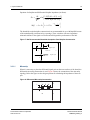
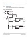
Figure 9: Equation
λ = εr × c f
1 λ3rd = 3×10 m / s εr
20
20× f 3rd
8
In the case of the 3.125 Gb/s data rate, the rise and fall times must be less than 40 pS. This
relates to an upper frequency of 25Ghz and a corresponding wavelength of 25 mm based on a
permittivity of 4.3. Therefore, the stitching vias must not be further apart than 8 mm.
Tundra Semiconductor Corporation
www.tundra.com
Tsi578 Hardware Manual
80B803A_MA002_07
48
3. Layout Guidelines
3.3.1.4
Via Construction
Due to the high frequency content of the Serial RapidIO signals, it is necessary to minimize the
discontinuities imposed by crossing ground and power planes when it is necessary to transition
to different signal layers. The use of a controlled impedance via is recommended The
construction of a differential via is shown in Figure 10.
Detailed design information can be found in bibliography entry 15, “Designing
Controlled Impedance Vias” by Thomas Neu, EDN Magazine October 2, 2003.
p
Ti
Figure 10: Differential Controlled Impedance Via
4 vias connected
to ground planes
Differential Signal
Signal Via Anti-pad which
touches the ground vias
Reference ground plane
Reference ground plane
3.3.1.5
Layer Transitioning with Vias
The basic rule in high speed signal routing is to keep vias in the signal path down to a minimum.
Vias can represent a significant impedance discontinuity and should be minimized. When
routing vias, try to ensure that signals travel through the via rather than across the via.
A via where the signal goes through the via, has a much different effect than a via where the
signal travels across the via. These two cases are shown in Figure 13 and in Figure 14. The “in”
and “out” nodes of the via model are shown on the their corresponding locations in the figures.
Transitioning across a via that is not blind or buried leaves a stub which appears as a capacitive
impedance discontinuity. The portion of the via that conducts current appears inductive while
the stub that develops only an electric field will appear capacitive.
Tsi578 Hardware Manual
80B803A_MA002_07
Tundra Semiconductor Corporation
www.tundra.com
3. Layout Guidelines
49
In order to minimize the effects of a via on a signal, the following equations may be used to
approximate the capacitance and inductance of the via design. It can be seen that the proximity
of the pad and antipad have a direct relationship on the capacitance, and that the length of the
barrel (h) has a direct effect on the inductance.
Figure 11: Equation
1.41ε r TD 1
C = -------------------------D2 – D 1
4h
L = 5.08h ln ⎛ ------⎞ + 1
⎝ d⎠
C is the capacitance in pF.
T is the thickness of the circuit board or thickness of pre-preg.
D1 is the diameter of the via pad.
D2 is the diameter of the antipad.
εr is the dielectric constant of the circuit board material.
L is the inductance in nH.
h is the overall length of the via barrel.
d is the diameter of the via barrel.
Figure 12: Via Construction
D2
D1
d
T
h
T
Tundra Semiconductor Corporation
www.tundra.com
Tsi578 Hardware Manual
80B803A_MA002_07
50
3. Layout Guidelines
Figure 13: Signal Across a Via
Via
Signal
Signal
"In"
Pwr & Gnd Planes
Stub
"Out"
Figure 14: Signal Through a Via
Via
Signal
"In"
Pwr & Gnd Planes
Signal
"Out"
Because of the high frequencies present in the RapidIO signal, vias become a significant
contributor to signal degradation. Most vias are formed by a cylinder going through the PCB
board. Because the via has some length, there is an inductance associated with the via. Parasitic
capacitance comes from the power and ground planes through which the via passes. From this
structure we model the via in RLC lumps as shown in Figure 15 and Figure 16. Cvia is the total
capacitance of the via to ground or power, Rvia is the total resistance through the via, and Lvia
is the total inductance of the via. These parameters may be extracted using 3D parasitic
extraction tools. By distributing the R, L, and C, the model better represents the fact that the
capacitance, resistance and inductance are distributed across the length of the via. For the Via
model to be accurate in simulation, the propagation delay of each LC section should be less than
1/10 of the signal risetime. This is to ensure the frequency response of the via is modeled
correctly up to the frequencies of interest. More information may be found in reference [16].
Figure 15: Signal Transitioning Across a Via Simulation Model
Out
Lvia/3
In
Cvia/4
Tsi578 Hardware Manual
80B803A_MA002_07
Rvia/3
Lvia/3
Rvia/3
Cvia/4
Lvia/3
Rvia/3
Cvia/4
Cvia/4
Tundra Semiconductor Corporation
www.tundra.com
3. Layout Guidelines
51
Figure 16: Signal Transitioning Through a Via Simulation Model
Lvia/3
In
Rvia/3
Cvia/4
3.3.1.6
Lvia/3
Rvia/3
Cvia/4
Lvia/3
Rvia/3
Cvia/4
Out
Cvia/4
Buried Vs. Blind
The use of buried and blind vias is recommended because in both cases the signal travels
through the via and not across it. Examples of these two types of structures are shown in
Figure 17 and Figure 18.
Figure 17: Buried Via Example
Signal
Via
"In"
Pwr & Gnd Planes
Signal
"Out"
Figure 18: Blind Via Example
Signal
Via
"In"
Pwr & Gnd Planes
Signal
"Out"
3.3.1.7
Serpentine Traces
During layout, it is necessary to adjust the lengths of tracks in order to accommodate the
requirements of equal track lengths for pairs of signals. In the case of the differential signals,
this ensures that both the negative and positive halves of the signals arrive at the receiver
simultaneously, thus maximizing the data sampling window in the eye diagram. Creating a
serpentine track is a method of adjusting the track length.
Tundra Semiconductor Corporation
www.tundra.com
Tsi578 Hardware Manual
80B803A_MA002_07
52
3. Layout Guidelines
Ensure that the wave front does not propagate along the trace and through the crosstalk path
perpendicular to the parallel sections, as shown in Figure 19. The arrival of a wave front at the
receiver ahead of the wave front travelling along the serpentine route is caused by the
self-coupling between the parallel sections of the transmission line (Lp).
Figure 19: Serpentine Signal Routing
Lp
DRIVER
crosstalk path
RECIEVER
S
To maximize the signal integrity, clock lines should not be serpentine.
Figure 22 describes the guidelines for length matching a differential pair. If it is necessary to
serpentine a trace, follow these guidelines:
• Make the minimum spacing between parallel sections of the serpentine trace (see “S” in
Figure 19) at least 3 to 4 times the distance between the signal conductor and the reference
ground plane.
• Minimize the total length (see “Lp” in Figure 19) of the serpentine section in order to
minimize the amount of coupling.
• Use an embedded microstrip or stripline layout instead of a microstrip layout.
p
Ti
3.3.2
For a detailed discussion about serpentine layouts, refer to Section 12.8.5 of
“High-Speed Signal Propagation, Advanced Black Magic” by Howard Johnson and
Martin Graham.
Crosstalk Considerations
The Serial RapidIO signals easily capacitively couple to adjacent signals due to their high
frequency. It is therefore recommended that adequate space be used between different
differential pairs, and that channel transmit and receive be routed on different layers. Cross
coupling of differential signals results in an effect called Inter-Symbol Interference (ISI). This
coupling causes pattern dependent errors on the receptor, and can substantially increase the bit
error rate of the channel.
Tsi578 Hardware Manual
80B803A_MA002_07
Tundra Semiconductor Corporation
www.tundra.com
3. Layout Guidelines
3.3.3
53
Receiver DC Blocking Capacitors
The Serial RapidIO interface requires that the port inputs be capacitor coupled in order to isolate
the receiver from any common mode offset that may be present in the transmitter outputs. DC
blocking capacitors should be selected such that they have low dissipation factor and low series
inductance. The recommended capacitor value is 0.1uF ceramic in an 0402 size.
Figure 20 shows the recommended tracking and capacitor pad placement required. It will be
necessary to model and simulate the effects of the changed track spacing on the channel quality
and determine if any changes are required to the topology. An often used method of correcting
the decreased impedance caused by the larger capacitor mounting pads is to create a slot in the
shield plane below the capacitor bodies and soldering pads. Since the impedance change caused
by the slot is dependent on the capacitor geometry, core thickness, core material characteristics
and layer spacings, the size and shape of the slot will have to be determined by simulation.
Do not place the capacitors along the signal trace at a λ/4 increment from the
driver in order to avoid possible standing wave effects.
Figure 20: Receiver Coupling Capacitor Positioning Recommendation
3.3.4
Escape Routing
All differential nets should maintain a uniform spacing throughout a route. Separation of
differential pairs to go around objects should not be allowed. Figure 21 illustrates several
options for breaking out a differential pair from the Tsi578 device. The order of preference is
from A to D.
Case D below has a small serpentine section used to match the inter-pair skew of the differential
pair. In this case each serpentine section should be greater than 3 x W (W=width), and the gap
should not increase by more than 2x. Figure 22 illustrates these requirements.
Tundra Semiconductor Corporation
www.tundra.com
Tsi578 Hardware Manual
80B803A_MA002_07
54
3. Layout Guidelines
Figure 21: Escape Routing for Differential Signal Pairs
Figure 22: Differential Skew Matching Serpentine
3.3.5
Board Stackup
The recommended board stack up is shown in Figure 23. This design makes provision for four
stripline layers and two outer microstrip layers. Layers eight and nine are provisioned as
orthogonal low speed signal routing layers.
Tsi578 Hardware Manual
80B803A_MA002_07
Tundra Semiconductor Corporation
www.tundra.com
3. Layout Guidelines
55
Figure 23: Recommended Board Stackup
Tundra Semiconductor Corporation
www.tundra.com
Tsi578 Hardware Manual
80B803A_MA002_07
56
3.4
3. Layout Guidelines
Power Distribution
The Tsi578 is a high speed device with both digital and analogue components in its design. The
core logic has a high threshold of noise sensitivity within its 1.2 V operating range. However,
the analogue portion of the switch is considerably more sensitive.
The correct treatment of the power rails, plane assignments, and decoupling is important to
maximize Tsi578 performance. The largest indicator of poor performance on the Serial RapidIO
interfaces is the presence of jitter. The die, I/O, and package designs have all been optimized to
provide jitter performance well below the limits required by the Serial RapidIO specifications.
The guidelines provided below will assist the user in achieving a board layout that will provide
the best performance possible. The required decoupling by each voltage rail can be found in
Table 16 on page 59. The ripple specifications for each rail are maximums, and every effort
should be made to target the layout to achieve lower values in the design.
A solid, low impedance plane must be provided for the VDD 1.2V core supply referenced to
VSS. It is strongly recommended that the VDD and VSS planes be constructed with the intent of
creating a buried capacitance. The connection to the power supply must also be low impedance
in order to minimize noise conduction to the other supply planes.
A solid, low impedance plane must be provided for the SP_VDD 1.2V SerDes supply,
referenced to the VSS plane. This supply can be derived from the same power supply as VDD,
as long as a Kelvin connection is used. The preference however, is to use a separate power
supply.
p
Ti
The term Kelvin connection is used to describe a single point of contact so that
power from one power plane does not leak past the power supply pin into the other
power plane. The leadkage can be caused by the fact the output of a power supply is
a very low impedance point in order to be able to supply a large amount of current.
Because it is such a low impedance point, any noise presented to it by the power
plane is sent to ground.
A kelvin connection enables two power planes to be connected together at a single
point. Using this technique, the same power supply module can be used to provide
power to a noisy digital power plane (VDD), as well as a quiet analog power plane
(SP_AVDD).
The SPn_AVDD 3.3V SerDes analogue supply also needs low impedance supply plane. This
supply voltage powers the RapidIO receivers and transmitters, and their associated PLLs.
Connect all of the SPn_AVDD pins to this plane and decouple the plane directly to VSS. The
plane must be designed as a low impedance plane in order to minimize transmitter jitter and
maximize receiver sensitivity. Construction of this plane as a buried capacitance referenced to
VSS is suggested.
Tsi578 Hardware Manual
80B803A_MA002_07
Tundra Semiconductor Corporation
www.tundra.com
3. Layout Guidelines
57
The REF_AVDD pins provide power to the S_CLK distribution circuits in the switch. The
voltage should be derived from the SPn_VDD plane. One ferrite will suffice to isolate the
SPn_VDD from the REF_AVDD. Two decoupling capacitors should be assigned to each pin.
The VDD_IO supply powers the 3.3V I/O cells on the switch. This supply requires no special
filtering other than the decoupling to the VSS_IO plane. Connect the VSS_IO plane to the VSS
plane using a Kelvin connection.
3.5
Decoupling Requirements
This section deals with the subject of decoupling capacitors required by the Tsi578. To
accomplish the goal of achieving maximum performance and reliability, the power supply
distribution system needs to be broken down into its individual pieces, and each designed
carefully. The standard model for representing the components of a typical system are shown in
Figure 24. This figure graphically represents the parasitics present in a power distribution
system.
Figure 24: System Power Supply Model
Power Delivery System
Decoupling
Vdd Power
Substrate
Tsi574 Die
Lpcb Rpcb
Rp
Rdc
Rsb
Lp
Ldc
Lsb
Cp
Cdc
Csb
+
-
3.5.1
Component Selection
The recommended decoupling capacitor usage for the Tsi578 is shown in Table 16 on page 59.
The capacitors should be selected with the smallest surface mount body that the applied voltage
permits in order to minimize the body inductance. Ceramic X7R type are suggested for all of the
values listed. The larger value capacitors should be low ESR type.
The components should be distributed evenly around the device in order to provide filtering and
bulk energy evenly to all of the ports.
Use the Tsi578 ball map (available at www.tundra.com) to aid in the distribution of
the capacitors.
Tundra Semiconductor Corporation
www.tundra.com
Tsi578 Hardware Manual
80B803A_MA002_07
58
3.5.1.1
3. Layout Guidelines
REF_AVDD
The REF_AVDD pins require extra care in order to minimize jitter on the transmitted signals.
The circuit shown in Figure 25 is recommended for the REF_AVDD signal. One filter is
required for the two pins.
Figure 25: PLL Filter
120 Ω @1.5A
SP_VDD (1.2V)
REF_AVDD (pin C24)
0.01uF
0.1uF
REF_AVDD (pin C26)
0.01uF
3.5.1.2
0.1uF
SPn_AVDD
The circuit shown in Figure 26 is recommended for the SPn_AVDD signal.
Figure 26: Analog Resistor
190
In this design Vtt can be controlled to be between 1.2 V and 3.3 V. For the Tsi578
operation Vtt is set to be 3.3V which provides the required voltage for SPx_AVDD.
Tsi578 Hardware Manual
80B803A_MA002_07
Tundra Semiconductor Corporation
www.tundra.com
3. Layout Guidelines
59
Table 16: Decoupling Capacitor Quantities and Values Recommended for the Tsi578
Voltage
Usage
Acronym
1.2V
Logic Core
VDD
20 x 0.1uF
20 x 0.01uF
16 x 1nF
-
16 x 22uF
1.2V
SerDes core,
SerDes bias
SP_VDD
16 x 0.1uF
16 x 0.01uF
32 x 1nf
8 x 10uF
8 x 100uF
3.3V
SerDes
transceivers
SPn_AVDD
16 x 0.1uF
16 x 0.01uF
-
-
-
3.3V
Single ended I/O
ports
VDD_IO
12 x 0.1uF
12 x 0.01uF
-
-
-
1.2V
Clock distribution
circuit
REF_AVDD
2 x 0.1uF
2 x 0.01uF
-
3.5.2
Component Requirements
1 x ferrite bead 120 ohm
@ 1.5Amp
Effective Pad Design
Breakout vias for the decoupling capacitors should be kept as close together as possible. The
trace connecting the pad to the via should also be kept as short as possible with a maximum
length of 50mils. The width of the breakout traces should be 20mils, or the width of the pad.
Via sharing should not be used in board design with the Tsi578.
Figure 27: Recommended Decoupling Capacitor Pad Designs
3.5.3
Power Plane Impedance and Resonance
The intent of adding decoupling to a board is to lower the impedance of the power supply to the
devices on the board. It is necessary to pay attention to the resonance of the combined bulk
capacitance and to stagger the values in order to spread the impedance valleys broadly across
the operating frequency range. Figure 29 demonstrates the concept of staggered bands of
decoupling. Calculate the impedance of each of the capacitor values at the knee frequency to
determine their impact on resonance.
Tundra Semiconductor Corporation
www.tundra.com
Tsi578 Hardware Manual
80B803A_MA002_07
60
3. Layout Guidelines
Figure 28: Equation
0.5
Fknee = ----------- whereT rise = time from 10% to 90%
T rise
Figure 29: Decoupling Bypass Frequency Bands
As the frequency changes, each part of the power distribution system responds proportionally;
the low-impedance power supply responds to slow events, bulk capacitors to mid-frequency
events, and so forth.
Tsi578 Hardware Manual
80B803A_MA002_07
Tundra Semiconductor Corporation
www.tundra.com
3. Layout Guidelines
3.6
61
Clocking and Reset
This section discusses the requirements of the clock and reset inputs.
3.6.1
Clock Overview
The Tsi578 switch input reference clocks that are used to drive the switch’s internal clock
domains.
Figure 30: Tsi578 Clocking Architecture
2
I C_SCLK
pin
2
I C
pin
Internal
registers
and bus
P_CLK
Internal Switching
Fabric
S_CLK_p/n
pin
Serial Port 0
clk gen
Serial Port 0
logic
Serial Port 1
logic
Serial Port 14
clk gen
Serial Port 14
logic
Serial Port 15
logic
Tundra Semiconductor Corporation
www.tundra.com
rxclka
rxclkb
rxclkc
rxclkd
Serial Port 0
SerDes
txclk
rxclka
rxclkb
rxclkc
rxclkd
Serial Port 14
SerDes
txclk
Tsi578 Hardware Manual
80B803A_MA002_07
62
3. Layout Guidelines
The reference clocks are described in Table 17. For more information about special line rate
support see “Clocking” on page 69.
Table 17: Clock Input Sources
Maximum
Clock Input Pin
Type
Frequency
S_CLK_[p/n]
Differential
156.25 MHz
Clock Domain
Serial Transmit Domain (Nominally 156.25MHz)
Internal Switching Fabric (ISF) Domain
P_CLK
3.6.1.1
Single Ended
100 MHz
Internal Register Domain and I2C Domain
Frequencies Required
The clock signals should be shielded from neighboring signal lines using ground traces on either
side. This reduces jitter by minimizing crosstalk from the neighboring signal lines. Since
P_CLK is single-ended, extra precaution should be taken so that noise does not get coupled onto
it.
In order to preserve the quality of the low jitter 156.25 MHz clock, the shielding requirement of
the clock lines is critical. It is possible that low-frequency noise can interfere with the operation
of PLLs, which can cause the PLLs to modulate at the same frequency as the noise. The
high-frequency noise is generally beyond the PLL bandwidth which is about 1/10th the S_CLK
frequency. For more information, refer to Figure 4 on page 38.
Tsi578 Hardware Manual
80B803A_MA002_07
Tundra Semiconductor Corporation
www.tundra.com
3. Layout Guidelines
3.6.1.2
63
Stability, Jitter and Noise Content
The maximum input jitter on the S_CLK input is 3pS RMS from 1.5 to 10 Mhz to avoid passing
through the PLL loop filter in the SerDes and affecting the transmit data streams. The maximum
input jitter allowable on the P_CLK input is 300 pSpp. Jitter on this input would be reflected
outside of the chip on the I2C bus. For more information, refer to Figure 4 on page 38.
Jitter Equation
The following equation can be used to convert Phase Noise in dBc to RMS jitter:
RMSjitter pS(rms) = [((10(dBc/10))1/2) * 2] / [2 * pi * (frequency in hz)]
Using this equation, an example of 312.5 MHz and a phase noise of -63dBc, would produce
0.72pS RMS jitter.
3.6.2
Clock Domains
Table 18: Tsi578 Clock Domains
Clock Domain
Clock Source
Description
Internal Register Domain
P_CLK
This clock domain includes all of the internal registers and their
interconnect bus.
The domain uses the input P_CLK directly.
Internal Switching Fabric
Domain
S_CLK_[p/n]
This clock domain includes the switching matrix of the ISF and
the portion of each RapidIO block that interfaces to the ISF.
I2C Domain
P_CLK divided by 1000
This clock domain is responsible for driving the I2C output clock
pin I2C_SCLK.
This clock domain is generated by dividing the P_CLK input by
1000.
The majority of the I2C logic runs in the Internal Register
Domain
Serial Transmit Domain
3.6.2.1
S_CLK_[p/n]
This clock domain is used to clock all of the Serial RapidIO
transmit ports.
Interfacing to the S_CLK_x inputs
The interface for a LVPECL clock source to the receiver input cell is shown in Figure 31. Note
that an AC-coupled interface is required so that only the AC information of the clock source is
transmitted to the clock inputs of the Tsi578.
Tundra Semiconductor Corporation
www.tundra.com
Tsi578 Hardware Manual
80B803A_MA002_07
64
3. Layout Guidelines
Figure 31: Tsi578 driven by LVPECL or CML clock source
Tsi574
Clock Source
S_CLK_p
PCB Traces
S_CLK_n
LVPECL / CML
The interface for an LVDS clock source to the converter cell is shown in Figure 32. Since an
LVDS driver requires a DC termination path, a 2-K. resistor should be inserted before the
capacitors. This resistor can be placed anywhere along the signal path between the clock source
and the AC-coupling capacitors, although Tundra recommends placing it close to the clock
source.
Note that the effective termination resistance seen by the clock source is about 95Ω. due to the
parallel combination of this external resistor and the integrated termination resistor of the
converter cell. Again, an AC-coupled interface is required so that only the AC information of
the clock source is transmitted to the clock inputs of the Tsi578.
Figure 32: Tsi578 driven by an LVDS clock source
Tsi574
Clock Source
S_CLK_p
2KΩ PCB Traces
S_CLK_n
LVDS
3.6.3
Reset Requirements
The Tsi578 requires only one reset input, HARD_RST_b. The signal provided to the device
must be a monotonic 3.3V swing that de-asserts a minimum of 1mS after supply rails are stable.
The signal de-assertion is used to release synchronizers based on P_CLK which control the
release from reset of the internal logic. P_CLK must therefore be operating and stable before the
1mS HARD_RST_b countdown begins.
Tsi578 Hardware Manual
80B803A_MA002_07
Tundra Semiconductor Corporation
www.tundra.com
3. Layout Guidelines
65
TRST_b must be asserted while HARD_RST_b is asserted following a device power-up to
ensure the correct setup of the tap controller. TRST_b is not required to be re-asserted for non
power cycle assertions of HARD_RST_b.
p
Ti
The most versatile solution to this requirement is to AND the HARD_RST_b and
TRST_b signals together to form an output with which to drive the TRST_b pin on
the switch.
Power up option pins are double sampled at the release of HARD_RST_b. As such, there is no
set-up time requirement, but the signals must be stable at the release of HARD_RST_b. There is
a hold time requirement of 100nS or 10 P_CLK cycles minimum.
3.7
Modeling and Simulation
The need for verifying the signal integrity of the board design is very important for designs
using GHz signalling. Tundra recommends that the designer invest in a simulation tool as an aid
to a successful RapidIO design. Tools are available from companies such as Mentor Graphics
(HyperLynx GHZ), Ansoft (SIwave) and SiSoft (SiAuditor). This is by no means a complete
list, only a sample of known suppliers.
3.7.1
IBIS
The use of IBIS for signal integrity checking at the high frequencies of the Serial RapidIO link
have been found to be too inaccurate to be useful. Also, we have found that most tools do not
yet support the IBIS Specification (Revision 3.2) for the support of multi-staged slew rate
controlled buffers. Tundra is making available an IBIS file which supports the LVTTL pins on
the device. Please contact Tundra Applications Engineering to obtain the file.
3.7.2
Encrypted HSPICE
Please contact the Tundra Applications Engineering through the web based form at
www.tundra.com/support to request the necessary Model License Agreement form required to
acquire the encrypted model.
Tundra Semiconductor Corporation
www.tundra.com
Tsi578 Hardware Manual
80B803A_MA002_07
66
3.8
3. Layout Guidelines
Testing and Debugging Considerations
It is prudent to make provision for debugging and testing tools in order to speed board bring-up.
This section provides information on the probing requirements for monitoring the serial
RapidIO link between two devices. At GHz frequencies, standard probing techniques are
intrusive and cause excessive signal degradation introducing additional errors in the link stream.
The recommended solution is an ultra low capacitance probe that operates in conjunction with a
logic analyzer. The addition of the appropriate disassembler software to the analyzer makes it a
very powerful tool for examining the traffic on a link and aiding in software debugging. Please
contact your local test equipment vendor for appropriate solutions for your requirements.
3.8.1
Logic Analyzer Connection Pads
The pinout for a recommended SRIO 8-channel probe is given in Table 19. This pin/signal
assignment has been adopted by several tool vendors including Tektronix, but is not an
established standard.
These notes are given here:
Footprint Channel vs. Lane/Link Designations
3.8.1.1
•
Channel = either an upstream OR downstream differential pair for a given lane
•
C<letter> = the designator for a channel which accepts a given differential pair of signals
•
C<letter><p or n> = the two signals of the differential pair. The signals within a given pair
may be assigned to either P or N regardless of polarity.
General Rules for Signal Pair Assignment of Analyzer Probe
The differential pairs that make up the SRIO links must be assigned to specific pins of the
footprint in order to take advantage of the pre-assigned channel assignments provided by Nexus
when purchasing the SRIO pre-processor.
Table 19: 8-Channel Probe Pin Assignment
Pin #
Signal Name
Pin #
Signal Name
2
GND
1
CAp/Tx0
4
CBp/Rx0
3
CAn/Tx0
6
CBn/Rx0
5
GND
8
GND
7
CCp/Tx1
10
CDp/Rx1
9
CCn/Tx1
12
CDn/Rx1
11
GND
Tsi578 Hardware Manual
80B803A_MA002_07
Tundra Semiconductor Corporation
www.tundra.com
3. Layout Guidelines
67
Table 19: 8-Channel Probe Pin Assignment
Pin #
Signal Name
Pin #
Signal Name
14
GND
13
CEp/Tx2
16
CFp/Rx2
15
CEn/Tx2
18
CFn/Rx2
17
GND
20
GND
19
CGp/Tx3
22
CHp/Rx3
21
CGn/Tx3
24
CHn/rX3
23
GND
Figure 33: Analyzer Probe Pad Tracking Recommendation
Tundra Semiconductor Corporation
www.tundra.com
Tsi578 Hardware Manual
80B803A_MA002_07
68
3.8.2
3. Layout Guidelines
JTAG Connectivity
The Joint Test Action Group (JTAG) created the boundary-scan testing standard (documented in
the IEEE 1149.1 Standard) for testing printed circuit boards (PCBs).
The boundary-scan approach involves designing boundary-scan circuitry into the integrated
circuit. PCBs populated with 1149.1 compliant devices can be then tested for connectivity,
correct device orientation, correct device location, and device identification. All the pins on
compliant devices can be controlled and observed using (typically) five pins that are routed to
the board edge connector. Board designers can develop a standard test for all 1149.1 compliant
devices regardless of device manufacturer, package type, technology, or device speed.
In addition to the 1149.1 compliant boundary scan TAP controller, the Tsi578 also contains an
1149.6 compliant TAP controller to aid in the production testing of the SERDES pins.
The Tsi578 also has the capability to read and write all internal registers through the JTAG
interface. Through this interface, users may load and modify configuration registers and look up
tables without the use of RapidIO maintenance transactions or an I2C EEPROM. Please visit the
Tundra web site at www.tundra.com to download the JTAG software to use to access the
internal registers.
Please visit the Tundra web site to download the BSDL file for the Tsi578.
3.9
Reflow Profile
The Tsi578 adheres to JEDEC-STD-020C for its reflow profile. For the leaded version, the peak
reflow temperature is 225oC (+0/-5oC). For the lead-free version, the peak reflow temperature is
260oC (+0/-5oC).
Tsi578 Hardware Manual
80B803A_MA002_07
Tundra Semiconductor Corporation
www.tundra.com
®
A.
69
Clocking
This appendix describes device behaviour outside the specified or recommended operating line rates
and clock frequencies.
The following topics are discussed:
A.1
•
“Line Rate Support” on page 69
•
“P_CLK Programming” on page 70
Line Rate Support
The Tundra Tsi578 supports all of the RapidIO Interconnect Specification (Revision 1.3) specified line
rates of 1.25, 2.50, and 3.125 Gbaud. The device also supports line rates that are outside of the RapidIO
specification. The ability to support multiple line rates gives the Tsi578 flexibility in both application
support and power consumption.
Table 20 shows the supported line rates for the Tsi578. The Serial Port Select pin, SP_IO_SPEED[1,0]
must be set to the values shown in Table 20 to achieve the documented line rates.
Table 20: Tsi578 Supported Line Rates1
S_CLK_p/n (MHz)
Baud Rate (Gbaud)
SP_IO_SPEED[1,0]
Bit Settings
153.60
1.2288
0,0
153.60
2.4576
0,1
153.60
3.0720
1,0
156.25
1.2500
0,0
156.25
2.5000
0,1
156.25
3.1250
1,0
125.00
2.5000
1,0
1. This information assumes a +/- 100 ppm clock tolerance that must be
obeyed between link partners
All bit and register settings that are documented for operation with S_CLK = 156.25 .Mhz also apply to
the use of 153.6 Mhz and 125 Mhz. Refer to “Clocking and Reset” on page 61 for more clocking
information.
Tundra Semiconductor Corporation
www.tundra.com
Tsi578 Hardware Manual
80B803A_MA002_07
70
A.2
A. Clocking
P_CLK Programming
The Tsi578 recommends a P_CLK operating frequency of 100 MHz. However, the device also
supports P_CLK frequencies less than the recommended 100 MHz. The ability to support other
P_CLK frequencies gives the Tsi578 flexibility in both application support and design.
The minimum frequency supported by the P_CLK input is 25 Mhz. Operation above
100 Mhz or below 25 Mhz is not tested or guaranteed.
The following sections describe the effects on the Tsi578 when the input frequency of the P_CLK
source is decreased from the recommended 100 Mhz operating frequency.
A.2.1
RapidIO Specifications Directly Affected by Changes in the P_CLK
Frequency
The following sections describe how changing the P_CLK frequency to below the recommended
100 MHz operation affect the counters and state machines in the Tsi578 that are defined in the RapidIO
Interconnect Specification (Revision 1.3).
A.2.1.1
Port Link Time-out CSR
RapidIO Part 6: 1x/4x LP-Serial Physical Layer Specification Revision 1.3: Section
6.6.2.2 Port Link Time-out CSR (Block Offset 0x20)
The RapidIO Interconnect Specification (Revision 1.3) defines the Port Link Time-out CSR as follows:
The port-link time-out control register contains the time-out timer value for all ports on a device. This
time-out is for link events, such as sending a packet to receiving the corresponding acknowledge and
sending a link-request to receiving the corresponding link-response. The reset value is the maximum
time-out interval, and represents between three and six seconds.
Tundra Implementation
The Tsi578 supports this timer in the “RIO Switch Port Link Time Out Control CSR” on page 280.
Effects of changing the P_CLK frequency are shown in the following formula:
•
Time-out = 32/F x TVAL
— F is P_CLK frequency in MHz
— TVAL is the 24-bit counter setting
–
Tsi578 Hardware Manual
80B803A_MA002_07
Maximum TVAL decimal value of 16,777,215 (0xFFFFFF)
Tundra Semiconductor Corporation
www.tundra.com
A. Clocking
71
Effects of changing the P_CLK frequency and TVAL setting can be seen in Table 21.
Table 21: Timer Values with P_CLK and TVAL Variations
P_CLK Setting
TVAL Setting
Equation
Timer Value
25 MHz
2,343,750 (0x23C346)
32/25 x 2,343,750
3 seconds
25 MHz
4,687,500 (0x47868C)
32/25 x 4,687,500
6 seconds
50 MHz
4,687,500 (0x47868C)
32/50 x 4,687,500
3 seconds
50 MHz
9,375,000 (0x8F0D18)
32/50 x 9,375,000
6 seconds
50 MHz
16,777,215 (0xFFFFFF)
32/50 x 16,777,215
10.4 seconds
100 MHz
9,375,000 (0x8F0D18)
32/100 x 9,375,000
3 seconds
100 MHz
16,777,215 (0xFFFFFF)
32/100 x 16,777,215
5.4 seconds
A.2.1.2
RapidIO Part 6: 1x/4x LP-Serial Physical Layer Specification Revision 1.3: Section
4.7.3.2 State Machine Variables and Functions
SILENCE_TIMER_DONE
The RapidIO Interconnect Specification (Revision 1.3) defines the SILENCE_TIMER_DONE as
follows:
Asserted when the SILENCE_TIMER_EN has been continuously asserted for 120 +/- 40µs and the
state machine is in the SILENT state. The assertion of SILENCE_TIMER_DONE causes
SILENCE_TIMER_EN to be deasserted. When the state machine is not in the SILENT state,
SILENCE_TIMER_DONE is deasserted
Tundra Implementation
The Tsi578’s silence timer does not have user programmable registers. The silence timer is sourced
from the P_CLK and any changes to P_CLK are directly reflected in the timer timeout period.
Tundra Semiconductor Corporation
www.tundra.com
Tsi578 Hardware Manual
80B803A_MA002_07
72
A. Clocking
DISCOVERY_TIMER_DONE
The RapidIO Interconnect Specification (Revision 1.3) defines the DISCOVERY_TIMER_DONE as
follows:
Asserted when DISCOVERY_TIMER_EN has been continuously asserted for 12 +/- 4msec and the
state machine is in the DISCOVERY state. The assertion of DISCOVERY_TIMER_DONE causes
DISCOVERY_TIMER_EN to be deasserted. When the state machine is not in the DISCOVERY state,
DISCOVERY_TIMER_DONE is deasserted.
Tundra Implementation
The Tsi578’s discovery timer is programmed in the “RIO Port x Discovery Timer” on page 322. The
DISCOVERY_TIMER field is used by serial ports configured to operate in 4x mode. The
DISCOVERY_TIMER allows time for the link partner to enter its discovery state, and if the link
partner supports 4x mode, for all four lanes to be aligned.
The DISCOVERY_TIMER field is a 4-bit field whose value is used as a pre-scaler for a
17-bit counter clocked by P_CLK.
The DISCOVERY_TIMER has a default value of 9 decimal, but can be programmed to various values.
The results of changing the DISCOVERY_TIMER value and P_CLK are shown in Table 22.
Table 22: Timer Values with DISCOVERY_TIMER and P_CLK Variations
P_CLK Setting
DISCOVERY_TIMER
Setting
Equation
Timer Value
100 MHz
9 decimal
9 * 0x1FFFF * 1/ P_CLK
11.79 mS
100 MHz
9 decimal
9 * 131071 * 1/ P_CLK
11.79 mS
25 MHz
1 decimal
1 * 131071 * 1/25 MHz
5.24 mS
25 MHz
2 decimal
2 * 131071 * 1/25 MHz
10.48 mS
25 MHz
15 decimal
15 * 131071 * 1/25 MHz
78.6 mS
50 MHz
1 decimal
1 * 131071 * 1/ 50 MHz
2.62 mS
50 MHz
5 decimal
5 * 131071 * 1/ 50 MHz
13.1 mS
50 MHz
15 decimal
15 * 131071 *1/ 50 MHz
19.7 mS
100 MHz
1 decimal
1 * 131071 * 1/ 100 MHz
1.31 mS
100 MHz
9 decimal
9 * 131071 * 1/ 100 MHz
11.79 mS
100 MHz
15 decimal
15 * 131071 *1/ 100 MHz
19.7 mS
Tsi578 Hardware Manual
80B803A_MA002_07
Tundra Semiconductor Corporation
www.tundra.com
A. Clocking
A.2.1.3
73
RapidIO Part 8: RapidIO Error Management Extensions Specification: Section 2.3.2.9
Packet Time-to-live CSR (Block Offset 0x2C)
The RapidIO Interconnect Specification (Revision 1.3) defines the Packet Time-to-live register as
follows:
The Packet Time-to-live register specifies the length of time that a packet is allowed to exist within a
switch device. The maximum value of the Time-to-live variable (0xFFFF) shall correspond to 100
msec. +/-34%. The resolution (minimum step size) of the Time-to-live variable shall be (maximum
value of Time-to-live)/(2e16-1). The reset value is all logic 0s, which disables the Time-to-live function
so that a packet never times out. This register is not required for devices without switch functionality.
Tundra Implementation
The Tsi578’s “RIO Packet Time-to Live CSR” on page 303 specifies the length of time that a packet is
allowed to exist within a switch device. The maximum value of the Time-to-live variable (0xFFFF)
corresponds to 100 msec +/-34%. The resolution (minimum step size) of the Time-to-live variable is:
•
(maximum value of Time-to-live)/(2e16-1).
Due to the uncertainty of the arrival of a packet relative to clock edges, a packet’s time to live expiry
time is not precise, but falls within a range. The range is as follows:
•
Minimum time-to-live nS = {1/P_CLK x 132} x TTLVAL
•
Maximum time-to-live nS = {1/P_CLK x 198} x TTLVAL
The TTL field in the“RIO Packet Time-to Live CSR” on page 303 is a 16-bit counter with a maximum
decimal value of 65535.
The default value of TTL is 0, which disables the Time-to-live counter.
Table 23 shows the TTL counter values using different values for P_CLK.
Table 23: TTL Values with P_CLK Variations
P_CLK Setting
Equation
Timer Value
25 MHz
Minimum time-to-live nS =
{1/25Mhz x 132} x 1
5.28 uS
{1/25Mhz x 132} x 15782 (3DA6)
83.3 mS
{1/25Mhz x 198} x 15782 (3DA6)
124.9 mS
Minimum time-to-live nS =
{1/25Mhz x 198} x 65535
519 mS
Tundra Semiconductor Corporation
www.tundra.com
Tsi578 Hardware Manual
80B803A_MA002_07
74
A. Clocking
Table 23: TTL Values with P_CLK Variations
P_CLK Setting
Equation
Timer Value
50 MHz
Minimum time-to-live nS =
{1/50Mhz x 132} x 1
10.56 uS
{1/50Mhz x 132} x 31566 (7B4E)
83.3 mS
{1/50Mhz x 198} x 31566 (7B4E)
125 mS
Maximum time-to-live nS =
{1/50Mhz x 198} x 65535
259.5 mS
Minimum time-to-live nS =
{1/100Mhz x 132} x 1
132 nS
{1/100Mhz x 132} x 63132 (F69C)
83.3 mS
{1/100Mhz x 198} x 63132 (F69C)
125 mS
Maximum time-to-live nS =
{1/100Mhz x 198} x 65535 =
129.8 mS
100 MHz
Tsi578 Hardware Manual
80B803A_MA002_07
Tundra Semiconductor Corporation
www.tundra.com
A. Clocking
A.2.2
75
Tundra Specific Timers
The following sections describe how changing the P_CLK frequency to below the recommended
100 MHz operation affect the Tundra-specific counters and state machines in the Tsi578.
A.2.2.1
Dead Link Timer
The Dead Link Timer period is controlled by the DLT_THRESH field in the “SRIO MAC x Digital
Loopback and Clock Selection Register” on page 403.
Each time a silence is detected on a link, the counter is reloaded from this register and starts to count
down. When the count reaches 0, the link is declared dead, which means that all packets are flushed
from the transmit queue and no new packets are admitted to the queue until the link comes up.
The duration of the dead link timer is computed by the following formula:
•
2^^13 * DLT_THRESH * P_CLK period
— P_CLK is 100Mhz (which gives a P_CLK period of 10nS)
— Default value of DLT_THRESH is 0x7FFF (which corresponds to 32767)
•
Using these parameters, the populated formula is 8192*32767*10e-9 = 2.68 seconds
When enabled, this timer is used to determine when a link is powered up and enabled, but dead (that is,
there is no link partner responding). When a link is declared dead, the transmitting port on the Tsi578
removes all packets from its transmit queue and ensure that all new packets sent to port are dropped
rather than placed in the transmit queue.
The DLT_THRESH is a 15-bit counter with a maximum value of 32767. Table 24 shows equations
using different values for DLT_THRESH and P_CLK.
Table 24: Timer Values with P_CLK and DLT_THRESH Variations
P_CLK Setting
Equation
Timer Value
25 MHz
8192 * 1 * 1/25 MHz
327 uS
8192 * 32767 * 1/25 MHz
10.74 seconds
8192 * 1 * 1/50 MHz
163.8 uS
8192 * 32767 * 1/50 MHz
5.37 seconds
8192 * 1 * 1/100Mhz
81.9 uS
8192 * 32767 * 1/100Mhz
2.68 seconds
50 MHz
100 MHz
Tundra Semiconductor Corporation
www.tundra.com
Tsi578 Hardware Manual
80B803A_MA002_07
76
A.2.3
A. Clocking
I2C interface and Timers
The I2C interface clock is derived from the P_CLK. Decreasing the frequency of P_CLK causes a
proportional decrease in the I2C serial clock and affects the I2C timers. The timer values can be
re-programmed during boot loading but the changes does not take effect until after the boot load has
completed. As a result, a decrease from 100 Mhz to 50 Mhz of P_CLK causes a doubling of the boot
load time of the EEPROM. Once boot loading has completed, the new values take effect and the I2C
interface can operate at the optimum rate of the attached devices.
A.2.3.1
I2C Time Period Divider Register
The “I2C Time Period Divider Register” This register provides programmable extension of the
reference clock period into longer periods used by the timeout and idle detect timers.
USDIV Period Divider for Micro-Second Based Timers
The USDIV field divides the reference clock down for use by the Idle Detect Timer, the Byte Timeout
Timer, the I2C_SCLK Low Timeout Timer, and the Milli-Second Period Divider.
•
Period(USDIV) = Period(P_CLK) * (USDIV + 1)
•
P_CLK is 10 ns
•
Tsi578 reset value is 0x0063
MSDIV Period Divider for Milli-Second Based Timers
The MSDIV field divides the USDIV period down further for use by the Arbitration Timeout Timer,
the Transaction Timeout Timer, and the Boot/Diagnostic Timeout Timer.
A.2.3.2
•
Period (MSDIV) = Period(USDIV) * (MSDIV + 1)
•
Tsi578 reset value is 0x03E7
I2C Start Condition Setup/Hold Timing Register
The “I2C Start Condition Setup/Hold Timing Register” programs the setup and hold timing for the start
condition when generated by the master control logic. The timer periods are relative to the reference
clock.
This register is shadowed during boot loading, and can be reprogrammed prior to a chain operation
without affecting the bus timing for the current EEPROM.
START_SETUP Count for the START Condition Setup Period
The START_SETUP field defines the minimum setup time for the START condition; that is, both
I2C_SCLK and I2C_SD seen high prior to I2C_SD pulled low. This is a master-only timing parameter.
Ti
•
This value also doubles as the effective Stop Hold time.
p
Period (START_SETUP) = (START_SETUP * Period(PCLK))
— PCLK is 10ns
Tsi578 Hardware Manual
80B803A_MA002_07
Tundra Semiconductor Corporation
www.tundra.com
A. Clocking
77
— Reset time is 4.71 microseconds.
— Tsi578 reset value is 0x01D7
START_HOLD Count for the START Condition Hold Period
The START_HOLD field defines the minimum hold time for the START condition; that is, from
I2C_SD seen low to I2C_SCLK pulled low. This is a master only timing parameter.
A.2.3.3
•
Period (START_HOLD) = (START_HOLD * Period(P_CLK))
•
P_CLK is 10 ns
•
Reset time is 4.01 microseconds
•
Tsi578 reset value is 0x0191
I2C Stop/Idle Timing Register
The “I2C Stop/Idle Timing Register” programs the setup timing for the Stop condition when generated
by the master control logic and the Idle Detect timer.
Ti
p
The START_SETUP time doubles as the Stop Hold.
The Stop/Idle register is broken down as follows:
•
The timer period for the STOP_SETUP is relative to the reference clock
•
The timer period for the Idle Detect is relative to the USDIV period
•
The STOP_SETUP time is shadowed during boot loading, and can be reprogrammed prior to a
chain operation without affecting the bus timing for the current EEPROM.
STOP_SETUP Count for STOP Condition Setup Period
The STOP_SETUP field defines the minimum setup time for the STOP condition (that is, both
I2C_SCLK seen high and I2C_SD seen low prior to I2C_SD released high). This is a master-only
timing parameter.
•
Period(STOP_SETUP) = (STOP_SETUP * Period(P_CLK))
— P_CLK is 10ns
— Reset time is 4.01 microseconds
— Tsi578 reset value is 0x0191
Tundra Semiconductor Corporation
www.tundra.com
Tsi578 Hardware Manual
80B803A_MA002_07
78
A. Clocking
IDLE_DET Count for Idle Detect Period
The IDLE_DET field is used in two cases. First, it defines the period after reset during which the
I2C_SCLK signal must be seen high in order to call the bus idle. This period is needed to avoid
interfering with an ongoing transaction after reset. Second, it defines the period before a master
transaction during which the I2C_SCLK and I2C_SD signals must both be seen high in order to call the
bus idle.
This period is a protection against external master devices not correctly idling the bus.
•
Period(IDLE_DET) = (IDLE_DET * Period(USDIV)), where USDIV is the microsecond time
defined in the “I2C Time Period Divider Register”
A value of zero results in no idle detect period, meaning the bus will be sensed as idle
immediately.
— Reset time is 51 microseconds
— Tsi578 reset value is 0x0033
A.2.3.4
I2C_SD Setup and Hold Timing Register
The “I2C_SD Setup and Hold Timing Register” programs the setup and hold times for the I2C_SD
signal when output by either the master or slave interface. It is shadowed during boot loading, and can
be reprogrammed prior to a chain operation without affecting the bus timing for the current EEPROM.
SDA_SETUP Count for the I2C_SD Setup Period
The SDA_SETUP field defines the minimum setup time for the I2C_SD signal; that is, I2C_SD is set
to a desired value prior to rising edge of I2C_SCLK. This applies to both slave and master interface.
This value should be set to the sum of the I2C_SD setup time and the maximum rise/fall time
of the I2C_SD signal in order to ensure that the signal is valid on the output at the correct
time. This time is different than the raw I2C_SD setup time in the I2C Specification.
•
Period(SDA_SETUP) = (SDA_SETUP * Period(P_CLK)), where P_CLK is 10ns.
— Reset time is 1260 nanoseconds
— Tsi578 reset value is 0x007E
SDA_HOLD Count for I2C_SD Hold Period
The SDA_HOLD field defines the minimum hold time for the I2C_SD signal; that is, I2C_SD valid
past the falling edge of I2C_SCLK. This applies to both slave and master interface.
•
Period(SDA_HOLD) = (SDA_HOLD * Period(P_CLK)), where P_CLK is 10 ns.
— Reset time is 310 nanoseconds
— Tsi578 reset value is 0x001F
Tsi578 Hardware Manual
80B803A_MA002_07
Tundra Semiconductor Corporation
www.tundra.com
A. Clocking
A.2.3.5
79
I2C_SCLK High and Low Timing Register
The “I2C_SCLK High and Low Timing Register” programs the nominal high and low periods of the
I2C_SCLK signal when generated by the master interface.
It is shadowed during boot loading, and can be reprogrammed prior to a chain operation without
affecting the bus timing for the current EEPROM.
SCL_HIGH Count for I2C_SCLK High Period
The SCL_HIGH field defines the nominal high period of the clock, from rising edge to falling edge of
I2C_SCLK. This is a master-only parameter.
The actual observed period may be shorter if other devices pull the clock low.
•
Period(SCL_HIGH) = (SCL_HIGH * Period(P_CLK))
— P_CLK is 10 ns
— Reset time is 5.00 microseconds (100 kHz)
— Tsi578 reset value is 0x01F4
SCL_LOW Count for I2C_SCLK Low Period
The SCL_LOW field defines the nominal low period of the clock, from falling edge to rising edge of
I2C_SCLK. This is a master-only parameter.
The actual observed period may be longer if other devices pull the clock low.
•
Period(SCL_LOW) = (SCL_LOW * Period(P_CLK))
— P_CLK is 10 ns
— Reset time is 5.00 microseconds (100 kHz)
— Tsi578 reset value is 0x01F4
A.2.3.6
I2C_SCLK Minimum High and Low Timing Register
The “I2C_SCLK Minimum High and Low Timing Register” programs the minimum high and low
periods of the I2C_SCLK signal when generated by the master interface. It is shadowed during boot
loading, and can be reprogrammed prior to a chain operation without affecting the bus timing for the
current EEPROM.
SCL_MINH Count for I2C_SCLK High Minimum Period
The SCL_MINH field defines the minimum high period of the clock, from rising edge seen high to
falling edge of I2C_SCLK. This is a master-only parameter.
The actual observed period may be shorter if other devices pull the clock low.
•
Period(SCL_MINH) = (SCL_MINH * Period(P_CLK))
— P_CLK is 10 ns
— Reset time is 4.01 microseconds
— Tsi578 reset value is 0x0191
Tundra Semiconductor Corporation
www.tundra.com
Tsi578 Hardware Manual
80B803A_MA002_07
80
A. Clocking
SCL_MINL Count for I2C_SCLK Low Minimum Period
The SCL_MINL defines the minimum low period of the clock, from falling edge seen low to rising
edge of I2C_SCLK. This is a master-only parameter.
The actual observed period may be longer if other devices pull the clock low.
•
Period(SCL_MINL) = (SCL_MINL * Period(P_CLK))
— P_CLK is 10 ns
— Reset time is 4.71 microseconds
— Tsi578 reset value is 0x01D7
A.2.3.7
I2C_SCLK Low and Arbitration Timeout Register
The “I2C_SCLK Low and Arbitration Timeout Register” programs the I2C_SCLK low timeout and the
Arbitration timeout. The arbitration timer period is relative to the MSDIV period, and the I2C_SCLK
low timeout period is relative to the USDIV period.
SCL_TO Count for I2C_SCLK Low Timeout Period
The SCL_TO field defines the maximum amount of time for a slave device holding the I2C_SCLK
signal low. This timeout covers the period from I2C_SCLK falling edge to the next I2C_SCLK rising
edge. A value of 0 disables the timeout.
•
Period(SCL_TO) = (SCL_TO * Period(USDIV))
— USDIV is the microsecond time defined in the “I2C Time Period Divider Register”.
— The reset value of this timeout is 26 milliseconds
— Tsi578 reset value is 0x65BB
ARB_TO Count for Arbitration Timeout Period
The ARB_TO field defines the maximum amount of time for the master interface to arbitrate for the
bus before aborting the transaction. This timeout covers the period from master operation start (see
setting the START bit in the “I2C Master Control Register”) until the ACK/NACK is received from the
external slave for the slave device address. A value of 0 disables the timeout.
•
Period(ARB_TO) = (ARB_TO * Period(MSDIV))
— MSDIV is the millisecond time defined in “I2C Time Period Divider Register”.
— The reset value of this timeout is 51 milliseconds
–
This timeout is not active during the boot load sequence.
— Tsi578 reset value is 0x0033
Tsi578 Hardware Manual
80B803A_MA002_07
Tundra Semiconductor Corporation
www.tundra.com
A. Clocking
A.2.3.8
81
I2C Byte/Transaction Timeout Register
The “I2C Byte/Transaction Timeout Register” programs the Transaction and Byte time-outs. The timer
periods are relative to the USDIV period for the byte timeout, and relative to the MSDIV period for the
transaction timeout.
BYTE_TO Count for Byte Timeout Period
The BYTE_TO field defines the maximum amount of time for a byte to be transferred on the I2C bus.
This covers the period from Start condition to next ACK/NACK, between two successive ACK/NACK
bits, or from ACK/NACK to Stop/Restart condition. A value of 0 disables the timeout.
•
Period(BYTE_TO) = (BYTE_TO * Period(USDIV))
— USDIV is the microsecond time defined in “I2C Time Period Divider Register”.
— This timeout is disabled on reset, and is not used during boot load.
— Tsi578 reset value is 0x0000
TRAN_TO Count for Transaction Timeout Period
The TRAN_TO field defines the maximum amount of time for a transaction on the I2C bus. This
covers the period from Start to Stop. A value of 0 disables the timeout.
•
Period(TRAN_TO) = (TRAN_TO * Period(MSDIV))
— MSDIV is the millisecond time defined in “I2C Time Period Divider Register”.
— This timeout is disabled on reset, and is not used during boot load
— Tsi578 reset value is 0x0000
A.2.3.9
I2C Boot and Diagnostic Timer
The “I2C Boot and Diagnostic Timer” programs a timer used to timeout the boot load sequence, and
can be used after boot load as a general purpose timer.
COUNT Count for Timer Period
The COUNT field defines the period for the timer. The initial reset value is used for overall boot load
timeout. A value of 0 disables the timeout.
Ti
p
During normal operation, this timer can be used for any general purpose timing.
The timer begins counting when this register is written. If this register is written while the counter is
running, the timer is immediately restarted with the new COUNT, and the DTIMER/BLTO event is not
generated.
When the timer expires, either the BLTO or DTIMER event is generated, depending on whether the
boot load sequence is active. If FREERUN is set to 1 when timer expires, then the timer is restarted
immediately (the event is still generated), providing a periodic interrupt capability.
•
Period(DTIMER) = (COUNT * Period(MSDIV))
Tundra Semiconductor Corporation
www.tundra.com
Tsi578 Hardware Manual
80B803A_MA002_07
82
A. Clocking
— MSDIV is the millisecond period define in “I2C Time PeriodDivider Register”.
— The reset value for the boot load timeout is four seconds. If the boot load completes before the
timer expires, the timer is set to zero (disabled).
— Tsi578 reset value is 0x0FA0
A.2.4
Other Performance Factors
This section describes any other factors that may impact the performance of the Tsi578 if P-CLK is
programmed to operate lower than the recommended 100 MHz frequency.
A.2.4.1
Internal Register Bus Operation
The internal register bus, where all the internal registers reside, is a synchronous bus clocked by the
P_CLK source. A decrease in the P_CLK frequency causes a proportional increase in register access
time during RapidIO maintenance transactions, JTAG registers accesses, and I2C register accesses.
RapidIO Maintenance Transaction
Maintenance transactions use the internal register bus to read and write registers in the Tsi578. If the
P_CLK frequency is decreased, it may be necessary to review the end point’s response latency timer
value to ensure that it does not expire before the response is returned.
Changing the frequency of the P_CLK does not affect the operation or performance of the
RapidIO portion of the switch, in particular its ability to route or multicast packets between
ports.
JTAG Register Interface
Changing the P_CLK frequency affects accesses to the internal registers through the JTAG register
interface because the interface uses the internal register bus. However, since access to the registers
using the JTAG interface is largely a manual command line terminal operation using the Tundra JTAG
Register Interface Software (see www.tundra.com for more information), the decreased performance
will not be perceivable.
Boundary scan operations are not affected by a chance in the P_CLK frequency because these
transactions use the JTAG TCK clock signal and do not access the internal register bus.
Tsi578 Hardware Manual
80B803A_MA002_07
Tundra Semiconductor Corporation
www.tundra.com
®
B.
83
Ordering Information
This chapter discusses ordering information and describes the part numbering system for the Tsi578.
B.1
Ordering Information
When ordering the Tsi578 please refer to the device by its full part number, as displayed in Table 25.
Table 25: Tsi578 Ordering Information
B.2
Part Number
Frequency
Temperature
Package
Pin Count
TSI578-10GCL
1.25 - 3.125 Gbit/s
Commercial
FCBGA
675
TSI578-10GCLY
1.25 - 3.125 Gbit/s
Commercial
FCBGA (RoHS)
675
TSI578-10GIL
1.25 - 3.125 Gbit/s
Industrial
FCBGA
675
TSI578-10GILY
1.25 - 3.125 Gbit/s
Industrial
FCBGA (RoHS)
675
Part Numbering Information
The Tundra part numbering system is explained as follows.
Prototype version status
Operating environment
Package type
RoHS/Green compliance
Operating frequency
Product number
Tundra product identifier
Tsi NNN(N) - SS(S) E P G (Z#)
•
( ) – Indicates optional characters.
•
Tsi – Tundra system interconnect product identifier. All Tundra semiconductor product numbers
start with “Tsi.”
•
NNNN – Product number (may be three or four digits).
•
SS(S) – Maximum operating frequency or data transfer rate of the fastest interface. For operating
frequency numbers, M and G represent MHz and GHz. For transfer rate numbers, M and G
represent Mbps and Gbps.
Tundra Semiconductor Corporation
www.tundra.com
Tsi578 Hardware Manual
80B803A_MA002_07
84
B. Ordering Information
•
E – Operating environment in which the product is guaranteed. This code may be one of the
following characters:
— C - Commercial temperature range (0 to +70°C)
— I - Industrial temperature range (-40 to +85°C)
— E - Extended temperature range (-55 to +125°C)
•
P – The Package type of the product:
— B - Ceramic ball grid array (CBGA)
— E, L, J, and K - Plastic ball grid array (PBGA)
— G - Ceramic pin grid array (CPGA)
— M - Small outline integrated circuit (SOIC)
— Q - Plastic quad flatpack
•
G – Tundra products fit into three RoHS-compliance categories:
— Y - RoHS Compliant (6of6) – These products contain none of the six restricted substances
above the limits set in the EU Directive 2002/95/EC.
— Y - RoHS Compliant (Flip Chip) – These products contain only one of the six restricted
substances: Lead (Pb). These flip-chip products are RoHS compliant through the Lead
exemption for Flip Chip technology, Commission Decision 2005/747/EC, which allows Lead
in solders to complete a viable electrical connection between semiconductor die and carrier
within integrated circuit Flip Chip packages.
— V - RoHS Compliant/Green - These products follow the above definitions for RoHS
Compliance and meet JIG (Joint Industry Guide) Level B requirements for Brominated Flame
Retardants (other than PBBs and PBDEs).
•
Z# – Prototype version status (optional). If a product is released as a prototype then a “Z” is added
to the end of the part number. Further revisions to the prototype prior to production release would
add a sequential numeric digit. For example, the first prototype version of device would have a
“Z,” a second version would have “Z1,” and so on. The prototype version code is dropped once the
product reaches production status.
Tsi578 Hardware Manual
80B803A_MA002_07
Tundra Semiconductor Corporation
www.tundra.com